1
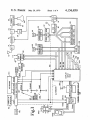
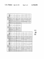
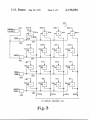
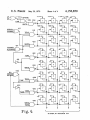
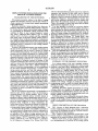
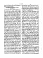
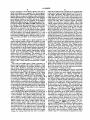
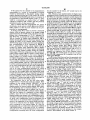
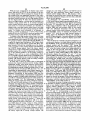
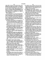
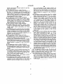
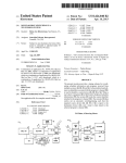
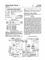
United States Patent [191
[11]
4,156,850
Beyers, Jr.
[45]
May 29, 1979
ch~Tune Assembly, Manual No. 7353, vol. 12, Sep.
[54] DISPLAY SYSTEM FOR FACILITATING
THE SETUP OF A TUNING SYSTEM
[75] Inventor:
[73] Assignee:
1976.
Farbfernsehgerat mit Mikroprozessor-Steurung-Wolf
Billy W. Beyers, Jr., Green?eld, Ind.
RCA Corporation, New York, NY.
gang Baum, Aug. 12, 1977, “Funkschau,” Heft 17.
Primary Examiner-Robert L. Grif?n
[21] Appl. No.: 828,848
[22] Filed:
Aug. 29, 1977
Assistant Examiner-Marc E. Bookbinder
[51]
Int. Cl.2 ............................................. .. H04B 1/26
[52]
US. Cl.‘
[58]
Field of Search ............. .. 325/453, 455, 459, 464,
325/468; 358/191, 192
‘ ‘
,
5/1977
ABSTRACT
In a tuning system for a television receiver including a
memory for storing binary signals representing tuning
which the binary signals representing the tuning volt
Tanaka ............................... .. 325/455
4,041,402
8/1977
Mogi
325/455
4,081,797
3/1978
Olson ......... ..
358/192
4,122,395
10/1978
Schotz et a1. ...................... .. 325/453
ages are generated in response to viewer control, a
multiplexer couples predetermined selected ones of the
binary signals representing the tuning voltages to a
digital channel number display unit to provide a viewer
with an indication of the relative tuning position. The
FOREIGN PATENT DOCUMENTS
1363048 8/1974 United Kingdom.
1377100 12/1974 United Kingdom.
1386935 3/ 1975 United Kingdom.
1410363 l0/l975 United Kingdom.
1445031 8/1976 United Kingdom.
1471712 4/1977 United Kingdom.
multiplexer also couples binary signals representing the
letter “A” to the channel number display during the
tuning voltage setup mode to distinguish the tuning
voltage setup mode from other modes of operation of
the tuning system. In addition, during a channel selec
tion setup mode, in which a viewer selects the channels
1485740 9/1977 United Kingdom.
he does not wish skipped during normal operation of
OTHER PUBLICATIONS
“Digitales
[57]
voltages corresponding to various channels a viewer
may select, during a tuning voltage setup mode in
References Cited
U.S. PATENT DOCUMENTS
4,023,107
Attorney, Agent, or Firm—Eugene M. Whitacre; Paul J.
Rasmussen; Peter M. Emanuel
............................... .. 325/455; 325/464;
358/192
[56]
'
the tuning system, the multiplexer couples binary sig
Programmspeicher-System"-Friedrich
nals representing the letters “Cl-I” to the channel num
Timmermann, Funkschau, Heft 17, Aug. 12, 1977.
Working With Microprocessors-Select the Station the
Micro Way-Quentin Scott-Electronics Weekly-Apr.
13, 1977.
General Instruments, AY-3-8330, Data Sheet.
Magnavox Service Manual-703777, Videomatic Tou
ber display to distinguish the channel selection tuning
POWER UP
mode from the tuning voltage setup mode and the nor
mal operating mode.
16 Claims, 4 Drawing Figures
KEYBOARD
TIMING AND CONTROL
ALTERNATES
up--- _
DN- -
4
DISPLAY
INPUT
MUX
MUX
.3
CHANNEL NUMBER DISPLAY
—r2‘o-—-'""
TUNING VOLT. REG.
136
US. Patent
May 29, 1979
4,156,850
Sheet 3 of 4
l2 6
)
MSDI l
NORMAL
CHANNEL
M130 0‘
30l
L/3l2b F
\soz
TENS
J,F____
13120
L___ .
l___
322
330
‘
LSD ll
3i
3|4c~
.
T
L_.
L4
B91
“1
T
3200
L, L1 320;! I
9
32Gb
TO DISPLAYIDECODER 124
Flg. 3
U
Sheet 4 of 4
+v
+v
4,156,850
+v
15g)
CH
ALTERNAT
k
J
Y
TO DISPLAY DECODER i241}
1
4,156,850
DISPLAY SYSTEM FOR FACILITATING THE
SETUP OF A TUNING SYSTEM
BACKGROUND OF THE INVENTION 7
2
only do electromechanical meters tend to be relatively
expensive and, because of their bulk, tend to detract
from the appearance of the receiver, but they may be
difficult to read by viewers not familiar with electronic
equipment. Moreover, electromechanical meters may
The present invention relates to the ?eld of tuning
systems for television receivers and the like which in
not provide suf?cient resolution between tuning posi
tions where the preferred channels are closely spaced.
clude a memory for storing binary signals representing
tuning information.
That is, for example, a viewer may not be able to distin
guish between channels 4, 5 or 6.
It is also possible to provide an on-screen display
system which provides an on-screen display showing a
scale calibrated in channel numbers (rather than in tun
Recently, electronic tuning systems have been pro
posed for television receivers which include a memory
for storing binary signals representing tuning voltages
for controlling an associated voltage controlled local _
oscillator in order to tune various channels a viewer
may select. Although these memory type of tuning
systems tend to be more versatile and less expensive
than other types of electronic tuning systems such as,
for example, those employing frequency synthesizers,‘
ing voltages) and a bar which changes length along the
scale as a tuning voltage is adjusted (see, for example,
the display disclosed in the “General Instrument AY-3
8330—Electronic On-Screen TV Tuning Scale” data
sheet available from General Instrument). While such
an on-screen display may overcome some of the disad
vantages of an electromechanical meter, it may never
ming by the manufacturer, and in some instances by the. 20 theless be dif?cult for a viewer to utilize because it
they suffer the disadvantage that at least some program
individual viewer, is required to enter tuning informa
provides information in the same analog format as does
tion into the memory.
an electromechanical meter. In addition, on-screen dis
In some of the proposed memory type tuning systems
the size of the memory, i.e., the number of locations in
which information can be stored, is limited to reduce
the cost of the tuning system. As a result, in these tuning
systems only the tuning information for a limited num
ber of preferred channels less than the total number of
play systems tend to add expense to the cost of the
tuning system and therefore may not be provided.
Thus, it is desirable that a memory type tuning system
include an arrangement for providing an indication of
tuning voltages in a format with which ordinary view
channels allocated to the television band can be stored.
ers are relatively familiar and which desirably include
provisions which tend to minimize the possibility of
Since the channels preferred by a particular viewer,
confusion on the part of a viewer.
either because of program content or because of the
reception conditions at the viewer’s location, are known
SUMMARY OF THE PRESENT INVENTION
only to a viewer, for those memory type tuning systems
In a tuning system of the type including memory
means for storing tuning information for various tuning
including a memory with only a limited number of
memory locations, programming is to be accomplished 35 positions a user may select, multiplexing means selec
by the viewer himself. Programming a memory type
tively couples binary signals corresponding to the tun
tuning system involves not only the selection of the
ing positions to a digital display unit so that tuning
preferred channels, but also involves the generation of
position symbols for identifying the tuning positions are
binary signals representing tuning voltages and channel
displayed during the normal operating mode of the
number display information corresponding to the pre 40 tuning system when information is retrieved from the
ferred channels. For viewers who are used to the con
memory to tune the receiver and couples binary signals
ventional type of mechanical tuning systems including a
representing the tuning voltages corresponding to the
mechanical rotary channel selector switch, the pro
tuning positions to the display unit so that numbers
gramming procedures for a memory type tuning system
related to the tuning voltages are displayed during a
may present considerable dif?culty and lead to unneces 45 programming mode in which the binary signals repre
sary costly and annoying service calls. Therefore, it is
senting the tuning voltages are generated for entry into
desirable that memory type tuning systems be arranged
the memory means.
to simplify as much as possible the required program
ming procedures.
One of the problems encountered in programming a
memory type tuning system is that of correlating a
viewable picture to a channel number. That is, as the
tuning voltage is adjusted until a viewable picture is
produced, unless a station identi?cation interval is for
tuitously transmitted while the viewable display is pres
ent or the viewer happens to know on what channel the
program being displayed is being transmitted, the
viewer has no way of knowing the channel to which the
receiver is presently tuned and cannot program the
corresponding channel number display information.
To overcome this problem, it is possible to provide an
electromechanical voltage meter which is responsive to
the analog tuning voltage so as to provide a viewer with
an indication of the relative tuning position (see, for
example, the tuning system disclosed in the “Magnavox
Service Manual—703777 Videomatic Touch Tune As
sembly," Manual No. 7353, File Volume 12, published
by the Magnavox Company, Fort Wayne, Ind.). Not
Desirably, the binary signals representing the tuning
voltages which are coupled to the display unit signals
are arranged in a predetermined format such that the
numbers displayed during the programming mode are
linearly related to the tuning voltages.
To further aid a viewer during the setup mode, binary
signals representing a predetermined symbol may be
coupled to the display means during the programming
mode to distinguish it from the normal mode of opera
tion.
BRIEF DESCRIPTION OF THE DRAWING
FIG. 1 shows, in block diagram form, a television
receiver employing a memory type tuning system with
provisions for facilitating its setup by a viewer in accor
dance with the present invention;
FIG. 2 shows a table indicating certain binary code
formats useful in facilitating an understanding of the
operation of the setup provisions shown in FIG. 1; and
FIGS. 3 and 4 show, in logic diagram form, respec
tive implementations of portions of the tuning system
4,156,850
3
facilitate its setup by a viewer.
4
dress register 114 is an up/down counter with provi
shown in block diagram form in FIG. 1 arranged to
sions for entering binary signals coupled to “jam” in
'
wise processed. The processed RF signals are coupled
puts, such as the CD4029 integrated circuit available
from RCA Corporation. The contents of address regis
ter 114 (as represented by the four binary signals) may
be increased by the decimal number 1 or decreased by
the decimal number 1 in response to the appropriate
control signals,'as will be described.
When a location of tuning voltage memory 112 is
to a mixer 16 where they are combined with a local
addressed, the contents of the addressed location are
DETAILED DESCRIPTION OF THE
INVENTION
In FIG. 1, RF (Radio Frequency) signals are re
ceived by an antenna 12 and coupled to an RF process
ing unit 14 where they are ?ltered, ampli?ed and other
oscillator signal generated by a local oscillator 18 to
“read” out of tuning voltage memory 112 and coupled
produce an IF (Intermediate Frequency) signal. The
frequency of the local oscillator signal is controlled in
to a digital-to-analog (D/A) converter 116 which con
verts them to the corresponding tuning voltages for
local oscillator 18.
A tuning voltage register 118, including 12 stages
tem 20 in accordance with the channel selected by a 5
arranged as an up/down counter for counting in
viewer so that when it is combined with the RF signals,
response to a tuning voltage generated by a tuning sys
.
the IF signal has modulated picture, color and sound
carriers at predetermined frequencies. The IF signal is
coupled to an IF processing unit 22 where it is ?ltered,
ampli?ed and otherwise processed. A portion of the IF
signal is coupled to an AFT (Automatic Fine Tuning)
straight binary format, is coupled to tuning voltage
memory 112 to generate l2 binary signals stored in each
memory location of tuning voltage memory 112 repre
senting the tuning voltage for each of the preferred
channels during a setup mode of operation of tuning
system 20. During the setup mode of operation of tun
discriminator which generates an AFT signal represent
ing a deviation between the picture carrier frequency
and its nominal value, e.g., in the United States, 45.75
ing system 20, the contents of tuning voltage register
is coupled to local oscillator 18 to modify the tuning
corresponding tuning voltages until the viewer is satis
118 are increased or decreased in increments of 1 in
MHz, which may occur due to component aging or 25 response to control signals generated under viewer
control and are converted by D/A converter 116 to
environmental operating conditions. The AFT voltage
voltage so as to minimize the deviation between the
picture carrier frequency and its nominal value. The
output of IF processing unit 22 is coupled to a signal
processing unit 26 which processes the various compo
nents of the IF signal so that a picture is produced by
?ed with the picture produced by kinescope 28. Se
lected ones of the binary signals generated by tuning
voltage register 118 are coupled to a channel number
display unit 120 so that numbers related to the tuning
voltage are displayed by which a viewer may verify
that the picture corresponds to the channel he wishes
programmed as is described below. The contents of
duced by means of a speaker 30.
Tuning system 20 is a memory type tuning system 35 tuning voltage register 118 are entered (“written”) into
the presently addressed memory location of tuning
which is capable of storing tuning information for tun
voltage memory 112 in response to viewer control.
ing a number of preferred channels less than the total
The channel number corresponding to a channel
number of channels allocated to the television band. For
selected by a viewer is displayed by channel number
example, while in the United States there are 82 chan
display unit 120 in response to binary signals generated
nels (2-83) allocated to the television band by the FCC
by a channel number register 122. Channel number
(Federal Communications Commission), tuning system
register 122 comprises two 4-stage up/down counters
20 may be programmed to tune only 16 channels which
means of a kinescope 28 and an audio response is pro
with provisions for entering binary signals at jam inputs
are preferred by a viewer over the others because of
such as CD4029 integrated circuits available from RCA
their program content or because of their relative recep
45 Corporation. Each counter generates four binary sig
tion characteristics at the viewer’s location.
Specifically, tuning system 20 includes a tuning volt
age memory 112 for storing the binary signals represent
ing the tuning voltages for each of 16 channels pre
ferred by the viewer. Tuning voltage memory 112 in
nals arranged in BCD (Binary Coded Decimal) format
(see the code con?gurations for decimal numbers 0-9 in
the table of FIG. 2 in the column labelled “BINARY”)
representing the ten decimal numbers 0-9. The binary
cludes 16 memory locations. Each of the memory loca 50 signals generated by the ?rst counter represent the least
signi?cant digit (LSD) of the decimal number and the
tions includes 12 memory cells for storing 12 respective
binary signalsgenerated by the second counter repre
binary signals or bits (binary digits) which have either a
logic “1” level corresponding to a relatively high volt
age +V or a logic “0” level corresponding to the volt
age at signal ground. The binary signals stored in each
memory location are arranged in straight binary format.
Straight binary format means that each of the 12 binary
signals represents a power of 2 from 0 to 11 and are
arranged in ascending order from right to left.
Each location of tuning voltage memory 112 has an
address. As will be described later, the tuning voltage
information for the preferred channels is stored in con
secutively addressed memory locations in ascending
channel number order. An address register 114 includ
sent the most signi?cant digit (MSD) of the channel
‘ number. The two counters are cascaded to count be
tween channel numbers 02 and 83 in either increasing or
or decreasing order in response to control signals gener
ated in response to viewer control.
In order to reduce the circuitry employed in display
unit 120, the binary signals representing the LSD and
MSD of the channel number are time multiplexed and
sequentially processed by channel number display unit
120. Speci?cally, the binary signals representing the
LSD are coupled to a display decoder 124 by a display
unit multiplexer (MUX) 126 during a UNITS timing
ing four stages is coupled to tuning voltage memory 112 65 signal and the binary signals representing the MSD are
coupled to display decoder 124 by display input multi
to generate four binary signals representing, in straight
plexer 126 during a TENS timing signal. A display
binary format, the decimal numbers 0-15 to address any
decoder 124 converts the four binary signals coupled to
of the 16 locations of tuning voltage memory 112. Ad
5
4,156,850
6
mined level when power is applied to the receiver after
it has been off and in response generates a PUP (Power
its input terminals to seven binary signals, each one of
which corresponds to a segment of a seven-segment
display unit. The seven binary output signals of display
UP) signal. Keyboard 144 includes push buttons la
decoder 124 are coupled to a display output multiplexer
(MUX) 128 which in turn couples them to units position
belled UP, DN (DowN), STORE and ERASE which
when depressed by a viewer cause corresponding com
mand signals to be generated and coupled to timing and
control unit 138. These command signals determine
whether the contents of address register 114, tuning
voltage register 118 and channel number register 122
seven-segment display unit 130A during the UNITS
timing signal and to the tens position seven-segment
display unit 130B during the TENS timing signal. Sev
en-segment display units 130A and 1303, which may be,
for example, of the light emitting diode or liquid crystal
are increased or decreased and whether data is stored in
or erased from tuning voltage memory 112 and skip
type, include seven segments a—g which are selectively
illuminated in response to the logic levels (i.e., either a
logic “0” or a logic “l”) of the respective binary signals ,
coupled to them to form the decimal numbers 0-9. To
MAl, CHANNEL and TUNE position for generating
form the number 9, for example, segments a, b, c, f and
g would be illuminated. The frequency and duty cycle
of the display timing signal are selected so that a viewer
does not notice any ?icker in the channel number dis
trolling the operation of tuning system 20 is de?ned by
corresponding signals to be generated in order to con
trol the operating mode of tuning system 20. The func
tional operation of control and timing unit 138 in con
the description set forth below. The structure of control
play.
The LSD and MSD binary signals generated by
memory 132. Mode selection switch 146 has a NOR
and timing unit 138 may comprise a logic con?guration
20 arranged to carry out the operations set forth below
channel number register 122 are also coupled to a skip
memory 132. Skip memory 132 is a memory containing
82 locations, each having a memory cell for storing one
bit. The addresses of the 82 locations of skip memory
132 correspond to the 82 channel numbers between 02 25
similar to the control and timing structure disclosed in
and 83. Thus, for example, when channel number regis
ter 122 contains binary signals representing channel
number 13, a corresponding memory location of skip
No. 4,123,713, hereby incorporated by reference. Alter
memory 132 will be addressed. The purpose of skip
memory 132 is to provide an indication, i.e., a logic “1”,
when a particular channel is to be skipped because it is
detail in copending United States Pat. application Ser.
No. 810,877 entitled, “Memory Type Tuning System
with Provisions to Facilitate Setup” ?led in the name of
Charles Martin Wine on June 28, 1977 now US. Pat.
nately, control and timing unit 138 may comprise a
microprocessor operated in accordance with a program
for carrying out the operations set forth below stored in
an associated memory such as is disclosed in an article
entitled, “Working with Microprocessors-Select the
Station the Micro Way” by Quentin Scott appearing in
the Apr. 13, 1977 issue of Electronics Weekly. The
numerous control interconnections between timing and
memory 132, a skip detector 134 generates a SKIP
35 control unit 138 and various portions of tuning system
signal.
20 have been omitted for the sake of clarity of drawing.
The LSD and MSD binary signals generated by
However, the function of these control interconnec
channel number register 122 are also coupled to a band
tions will become clear from the following description
selector 136, which may, for example, comprise a read
of the operation of tuning system 20.
only memory (ROM) to determine from the channel
number the frequency band in which the selected chan 40 In operation, assuming that mode selector switch 146
has been placed in its NORMAL position, when'the
nel resides and in response generate a representative
not one of the channels preferred by a viewer. In re
sponse to the presence of a logic “1” in a location of skip
band selection signal. Thus, for example, in the United
States, band selector 136 generates respective band
selection signals for channels 2-6, 7-13 and 1483. The
receiver is turned on, binary signals representing the
lowest channel number, i.e., channel number 02 (as
would be displayed .by‘ channel number display unit
band selection signals are coupled to local oscillator 18 45 120), are coupled to channel number register 122 from
unit 123 and binary signals representing the number 15
to control the frequency range in which it oscillates.
are coupled to address register 114 from unit 115 and
Local oscillator 18 includes arrangements of varactor
entered into the respective registers in response to the
diodes which are switched into an oscillator con?gura
tion in response to the respective band selection signals
generation of a PUP signal. At this point, vthe contents
to determine the frequency range in which local oscilla
tor 18 oscillates. The speci?c'frequency at which local
oscillator 18 oscillates is determined by the magnitude
of the location of skip memory 132 corresponding to
channel number 02 are examined by skip detector 134.
If a logic “1” is detected, a SKIP signal, representing
that channel 2 is not preferred and is to be skipped, is
generated. If a logic “0” is detected, a SKIP signal (i.e.,
of the tuning voltage.
The timing signals for controlling the sequential oper
ation of tuning system 20 are generated by a timing and
control unit‘ 138 by dividing a clock signal generated by
a clock oscillator into various timing intervals. The
control signals for controlling the transfer of informa
tion to and from tuning voltage memory 112 and skip
memory 132 and to control the counting operations of 60
address register 114, tuning voltage register 118 and
channel number register 122 in the manner set forth
below are generated in a timed sequence in response to
the logic complement of the SKIP signal), representing
that channel 2 is preferred and not to be skipped, is -,
generated and coupled to timing and control unit 138. Y
In response to a SKIP signal the contents of channel ‘
number register 122 are increased by a count of 1 and '_
the contents of the location of skip memory 132 corre
sponding to the next channel are examined. This pro
cess continues until a SKIP signal is generated. In re
sponse to a SKIP signal,‘ the contents of address register
114 are increased by a count of 1 but the contents of
the timing signals and in response to command signals
generated by a power up detector 142, a keyboard 144, 65 channel number register 122 are not further increased. .
At this point, the contents of channel number register
a mode selector switch 146 and skip detector 134.
Power up detector 142 detects when the power supply
voltage for tuning system 20 rises above a predeter
122 (which is the ?rst address of SKIP memory 132 at
which a logic “0” was detected) are displayed by chan
7
4,156,850
nel number display 120 and the contents of the ?rst
location of tuning voltage memory 112 are “read out”
and converted to a corresponding tuning voltage.
When a viewer wishes to change the channel, he may
do so by depressing either the UP or DN push button on
keyboard 144. When the UP push button is depressed,
the contents of channel number register 122 are succes
sively increased by a count of 1 until a SKIP signal is
generated by skip detector 134. When a SKIP signal is
generated, the contents of address register 114 are in
8
To program or reprogram the tuning voltage, the
viewer should place mode selector switch 146 in its
TUNE position and thereafter depress the UP and DN
push buttons on keyboard 144 to change the tuning
voltage by changing the contents of tuning voltage
register 118 until an acceptable picture is obtained on
the screen of kinescope 28.
At this point,~ the viewer must make surethe picture
corresponds to the selected channel for which tuning
voltage information is to be entered before the tuning
creased by a count of 1 but the contents of channel
number register 122 are not further increased. At this
voltage information is “written” into tuning voltage
point, the channel number of the second preferred chan
correspond to a different channel number than the one
memory 112. This is necessary because the picture may
displayed by channel number display 120 when mode
nel is displayed and the corresponding tuning voltage is
generated. The operation of tuning system 20 when a
DN push button has been depressed to change the chan
nel is similar to the operation of tuning system 20 when
selector switch 146 was in its CHANNEL position.
This may occur, for example, because the viewer has
the UP push button has been depressed to change the
channel, except that the contents of channel number
cause the RF carrier for the selected channel was not
tuned past the correct tuning voltage for the selected
channel to the tuning voltage for another channel be
register 122 and address register 114 are decreased by a 20 suf?ciently strong to produce an acceptable picture. Of
course, a viewer can verify that the display corresponds
count of 1 rather than being increased by a count of 1.
to the selected channel by waiting until a station identi
As was earlier noted, it is intended that tuning volt~
?cation signal is broadcast. However, considering that
age information for the channels preferred by a viewer
such a procedure must be followed for each of the pre
be stored in consecutive locations of tuning voltage
ferred channels to be programmed, this may involve
memory 112 in the same order as the corresponding
considerable time and is therefore undesirable.
channel numbers. To accomplish this, a viewer ?rst
In the present tuning system, the viewer may verify
places mode selector switch 146 in its CHANNEL
that the display corresponds to the selected channel to
position. In response to the generation of a CHANNEL
be programmed simply by referring to the display pro
signal, the contents of channel number register 122 and 30 duced by channel number display 120 after he has
the contents of address register 114 will be increased
placed mode selector switch 146 in its TUNE position.
until the channel number of the ?rst channel which has
When mode selector switch 146 is placed in its TUNE
a logic “0” in the associated location of skip memory
position, display input multiplexer 126 decouples the
132 is displayed and the associated location of tuning
binary signals generated by channel number register 122
voltage memory 112 is addressed in the same manner as 35 representing the LSD and MSD of the channel number
when a PUP signal is generated when power is ?rst
applied to the receiver. If none of the channels have
been programmed, channel number 02 will be displayed
by channel number display 120 and an unviewable pic
ture will be produced on the screen of kinescope 28
from the remainder of channel number display 120 and
instead couples selected ones of the binary signals gen
erated by tuning voltage register 118 representing the
tuning voltage to the remainder of channel number
display 120. As a result, channel number display 120
displays a decimal number approximately related to the
tuning voltage to provide a viewer with a relative indi
since no skip bits, i.e., logic “l’s” have been entered in
skip memory 132 and no meaningful tuning voltage
information is contained in tuning voltage memory 112.
cation of the tuning position. The selected binary signals
At this point, the viewer should program tuning system
generated by tuning voltage register 118 which are
20 to generate the appropriate tuning voltage to pro 45 coupled to display input multiplexer 126 to the remain
duce an acceptable display by placing mode selection
der of channel number display 120 are chosen so that
switch 146 into its TUNE mode and proceeding as is set
forth below. If some channels have been programmed,
the channel number for the ?rst channel which has a
TUNE mode is related in a linear fashion to the tuning
its quality.
board 144. In response to the generation of a STORE
the relative tuning voltage number displayed during the
voltage without portions in the range which will be
logic “0” in the associated location of skip memory 132 50 unintelligible or confusing to the average viewer as will
is displayed and the associated location of tuning volt
be explained below. By reference to a relative tuning
age memory 112 is addressed so that a viewable picture
voltage table which relates the tuning voltage number
is produced. At this point, the viewer may reprogram
displayed by channel number display 120 when tuning
tuning system 20 for this channel to generate an updated
system 20 is in the TUNE mode to respective channel
tuning voltage in the manner set forth below in order to 55 numbers, the viewer will be able to verify that the pic
attempt to improve the picture quality or may depress
ture obtained during the TUNE mode and the corre
the UP push button on keyboard 144 to select the next
sponding tuning voltage corresponds to the channel to
channel to be programmed, if an unacceptable picture is
be programmed.
produced, or reprogrammed, if the picture produced is
To enter the binary signals representing the tuning
viewable but the viewer wishes to attempt to improve 60 voltage, a viewer depresses the STORE button on key
If the viewer depresses the UP push button, the con
signal, the contents of tuning voltage register 118 are
tents of channel number register 122 are increased by a
transferred to and “written” into the presently ad
count of 1 until another SKIP signal is generated. At
dressed location of tuning voltage memory 112. Simul
this point, the channel number of the next already pro 65 taneously, in response to the STORE signal, a logic “0”
g'rammed preferred or unprogrammed channel is dis
(provided by a connection to signal ground) is coupled
played and the associated location of tuning voltage
to and “written” into the presently addressed location
of skip memory 132.
memory 112 is addressed.
4,156,850
9
If the picture for the channel to be programmed is
unacceptable to a viewer or corresponds to another
channel as determined by the relative tuning voltage
number displayed during the TUNE mode, the viewer
should depress the ERASE push button. In response to
the generation of the ERASE signal, a logic “1” (pro
10
for the number 9, the letters A-F would tend to be
confusing to a viewer.
FIG. 3 shows a logic implementation of display input
multiplexer 126 for coupling the six most signi?cant bits
Ell-B6 to the remainder of channel number display 120
in octal format in order to display a two digit number
voltage) is coupled to and “written” into the presently
linearly related to the'tuning voltage during the TUNE
mode of operation of tuning system 20. Display input
addressed location of skip memory 132.
multiplexer 126 of FIG. 3 comprises a 4X4 rectangular
vided by a connection to a source of the +V supply
‘
After a channel has been programmed, the viewer 0 array of transfer (T) gates 312a-d, 314a-d, and 318a-d.
Each transfer T gate has an input terminal 301, an out
should place mode selector switch 146 into its CHAN
put terminal 302 and a control terminal 303 for control
NEL position so that the next channel can be pro
ling the transfer of data between input terminal 301 to
grammed or reprogrammed.
output terminal 302. As long as a logic “0” is applied to
In tuning system 20, in order to provide a numerical
the control terminal 303 of a transfer gate, the input
display which is linearly related to the tuning voltage
terminal 301 is decoupled from the output terminal 302
generated during the TUNE mode, the three most sig~
ni?cant bits corresponding to 211-29, indicated by
Bll-B9 in FIG. 1, generated by tuning voltage register
118 are coupled by display input multiplexer 126 to
display decoder 124 instead of the binary signals repre
senting the MSD of the channel number during the
TENS timing signal and the next three most signi?cant
bits, corresponding to 23-26, indicated by B8-B6 in
FIG. 1, generated by tuning voltage register 118 are
coupled by display input multiplexer 128 to display
decoder 124 instead of the binary signals representing
the LSD of the channel number during the UNITS
timing signal. With this con?guration, as the contents of
tuning voltage register 118 are varied in a range from a
?rst extreme corresponding to the lowest magnitude
tuning voltage to a second extreme corresponding to
the highest magnitude tuning voltage, the numbers in
the tens and units display positions vary between 0 and
7 in accordance with the octal coding format indicated
so that whatever signal is coupled to input terminal 301
is prevented from affecting the condition of the signal
level at output terminal 302. When a logic “1” is applied
to control terminal 303 of a transfer gate, whatever
signal is coupled to its input terminal 301 is transferred
to its output terminal. The output terminal 302 of each
transfer gate in a column is coupled to a respective one
of four common output lines 320a-d. Output lines
320a-d of display input multiplexer ‘126 of FIG. 3 are
the four input lines of display decoder 124 of FIG. 1.
The input terminals of each transfer gate in a row is
coupled to a respective one of four common control
lines 322-328. The control signal on each one of control
lines 322-328 is generated by a respective one of four
AND gates 330-336.
It will be noted that there are four bits associated with
the tens and units positions of the channel number dis
play while there are only three bits associated with the
tens and units positions of the tuning voltage display. To
accommodate this difference, a logic “0,” provided by
in the column labelled “OCTAL” of the table of FIG. 2.
It will be noted that with the three bit octal format there
means of a connection to signal ground, is continually
are no code con?gurations after the code con?guration
coupled to input terminals 301 of transfer gates 316a and
for the number 7. Thus, with this octal format, there
318a of the rows associated with the tens and units
will be no code con?gurations generated for which
positions of the tuning voltage number display.
there is no available meaningful numerical display as is
The output of AND gate 330 will become a logic “‘1”
the case for the straight binary and hexidecimal code
and, as a result, the binary signals'representing the tens
formats discussed above. That is, when the octal format
position of the channel number, i.e., MSD3-MSDO
is utilized, channel number display 120 will change in a
corresponding to bit positions 23-20, will be transferred
linear relationship to the tuning voltage between num 45 to display decoder 124 only when the TENS timing
bers 00 and 77 without any gaps in which the display is
signal has a logic “1” level and either the NORMAL
not linearly related to the tuning voltage.
signal or CHANNEL signal, coupled to an OR gate
By comparison, this is not the case when either
338, has a logic “1” level. The output of AND gate 332
straight binary or hexidecimal codes are utilized. With
will become a logic “1” and, as a result, the binary
reference to the column labelled “BINARY” of the
signals representing the units position of the channel
table of FIG. 2, it will be noted that although each
number, i.e., LSD3-LSDO corresponding to bit posi
display position of channel number display 120 is capa
tions 23-29, will be transferred to display decoder 124,
ble of displaying only ten decimal numbers, i.e., 0-9, if
a four bit straight binary code is utilized, e.g., by cou
pling binary signals B11-B8 to channel number display
120, after the number 9 is displayed in either display
position, since the four bits corresponding to either
display position may assume code con?gurations corre
sponding to numbers greater than 9, i.e., numbers 10-15,
six more code con?gurations could be generated for
only when the UNITS timing signal has a logic “1”
level and either the NORMAL or CHANNEL signal
has a logic “1” level. The output of AND gate 334 will
become a logic “1”, and, as a result, binary signals
B11-B9 representing the tens position in octal format of
the tuning voltage number will be transferred to display
decoder 124 only when the TENS timing signal and the
TUNE signal have logic “1” levels. The output of
which there are no symbols which meaningfully corre
AND gate 336 will become a logic “1” and, as avresult,
spond to the magnitude of the tuning voltage and there
binary signals B8-B6 representing the units position of
the tuning voltage number will be transferred to display
decoder 124 only when the UNITS timing signal and
the TUNE signal have logic “1" levels. The binary
would be an interval when the display would not lin
early correspond to the tuning voltage. If a four bit
hexidecimal code, as is indicated in the column labelled
“HEXIDECIMAL’! of the table of FIG. 2, is utilized,
although letters A-F could be displayed for the six code
con?gurations remaining after the code con?guration
signals coupled to the display decoder 124 are decoded
in accordance with the code indicated in the column
labelled “DECODER” in the table of FIG. 2.
11
4,156,850
With the logic arrangement of display input multi~
12
changes at a rate which is equal to one-half the rate at
which the least signi?cant binary signal coupled to
channel number display 120, i.e., B9, changes, it has a
plexer 126 shown in FIG. 3, as the contents of the tun
ing voltage register 118 are changed to change the tun
ing voltage from one magnitude extreme to the other,
the tuning voltage number will change in a correspond
ing linear fashion between the two digit number 00 and
the two digit number 77. Since the channel number is
rate equal to one-half the rate at which the tuning. volt
age number displayed changes, and it is thus a desirable
, choice for this purpose.
To distinguish the CHANNEL mode from the
TUNE mode, binary signals representing the letter “C”,
provided by a unit 152, and binary signals representing
also a two digit number, a viewer may be confused as to
whether tuning system 20 is in its normal operating
mode, channel selection mode or tuning voltage adjust
the letter “H”, provided by a unit 154, are coupled to
display input multiplexer 126 to be displayed in tens
ment mode. To avoid such confusion, it is desirable to
display only a one digit number rather than a two digit
position 130B and units position 130A as the symbol
number to indicate the tuning voltage during the TUNE
“CH” (for CHannel) alternately with the two digit
mode. To further avoid confusion, it is desirable to
display a symbol to indicate to a viewer when tuning
system 20 is in the CHANNEL mode and another sym
bol when tuning system 20 is in the TUNE mode.
To display a one digit number rather than a two digit
channel number when mode selector switch 146 is in
the CHANNEL mode. To alternate the display of the
symbol “CH” with the two digit channel number, a
number representing the tuning voltage, only the three
most signi?cant binary signals, Bll-B9 (rather than the
20
two groups of binary signals B11-B9 and B8-B6), are
coupled to display input multiplexer 126. Display input
multiplexer 126 couples binary signals Bil-B9 to dis
timing signal ALTERNATE having, for example, a
period of approximately 2 seconds, generated by timing
and control unit 138 is coupled to display input multi
plexer 126.
FIG. 4 shows 4X7 transfer (T) gates arranged to: (l)
continuously display a two digit channel number during
the NORMAL mode; (2) alternately display a two digit
play decoder 124 and the resulting seven bit display
channel number and the symbol “CH” during the
code is coupled to units position display unit 130 during 25 CHANNEL mode; (3a) continually display the symbol
“AJ” when the tuning voltage is not being adjusted by
the UNITS timing signals. Since the binary signals
change from a code con?guration corresponding to the
decimal number 0 to a code con?guration correspond
ing to the decimalnumber 7 as the tuning voltage is
changed, there will be no code con?gurations which
are not capable of being displayed in an intelligible form
means of the UP and DN push buttons during the
TUNE mode; and (3b) display a one digit tuning volt
age number in units position 130A of the display and
alternately display the symbols “A” and “-” in tens
position 130B of the display when the tuning voltage is
being adjusted by means of the UP and DN push but
tons during the TUNE mode. The logic arrangement
by units display 130A and as a result the tuning voltage
number will change linearly with the tuning voltages
through the tuning voltage range.
shown in FIG. 4 is similar to that shown in FIG. 3. OR
In order that a viewer be better able to distinguish 35 gate 412, NAND gate 414, INVERTER 416 and AND
between the channel selection and the tuning voltage
adjustment modes, when mode selector switch 146 is
placed in the TUNE position, as long as the viewer is
not adjusting the tuning voltage by means of the UP and
DN push buttons of keyboard 144, the letter “A”, cor
responding to appropriately coded binary signals cou
pled to display input multiplexer 126 from a unit 148, is
displayed continually in tens position 130B and the
letter “J ,” corresponding to appropriately coded binary
signals coupled to display input multiplexer 126 from a
unit 156, is continually displayed in the units position so
that the symbol “AJ” for AdJustment is displayed.
When the viewer adjusts the tuning voltage by means of
the UP and DN push buttons, as the correspondingly
gates 418, 426, 422 and 424 control the transfer of infor
mation to display decoder 124 to accomplish functions
(1) and (2) set forth above. NOR gate 434 and‘AND
gates 436 and 438 control the transfer of information to
40 display decoder 124 to accomplish function (3a) set
forth above. NOR gate 440, INVERTER 416 and
.AND gates 428, 430 and 432 control the transfer of
information to display decoder 124 to accomplish func
tion (3b) set forth above. Display decoder 124 is ar
45 ranged to decode the groups of four binary signals cou
pled to it to form the desired number and symbols in
accordance with the code set forth in column labelled
“DECODER” of the table of FIG. 2.
To facilitate the setup of tuning system 20, it may also
be desirable to display symbols representing the tuning
changing one digit tuning voltage number is displayed
band in tens display position 130B next to the tuning
in units position 130A, the letter “A” is displayed in the
tens position 130B. Because only the three most signi?
voltage number displayed in units display position
cant binary signals B11-B9 are coupled to channel num
130A. To accomplish this, assuming that there are three
ber display unit 120, the tuning voltage will appear to
tuning bands, binary signals representing the letters
change very slowly and may tend to confuse a viewer
“A”, “B” and “C” corresponding to the ?rst, second
and third tuning bands, respectively, .may be coupled to
display input multiplexer 126. When a tuning voltage
into believing that the tuning voltage is not changing in
response to his control. To overcome this, binary sig
nals, provided by a unit 150 by means of corresponding
connections between the source of the voltage +V and
signal ground, representing the symbol “~” (dash) are
coupled to display input multiplexer 126 to be alter
nately displayed in place of the letter “A” in tens‘posi
tion 130B when the tuning voltage is being adjusted
during the TUNE mode. It is desirable to utilize a tim
for a channel in the ?rst band is generated, the binary
60
signals representing the letter “A” would be coupled by
display input multiplexer 126 to the remaining portion
of channel number display 120 so that the letter “A” is
displayed in tens position 130B and the corresponding
one digit tuning voltage number is displayed in units
position 130A and so on for the remaining two bands.
ing signal to cause display of the letter “A” and the 65 To detect the band, it is possible to utilize a modulo 3
up/down counter (i.e., an up/down counter having
symbol “—” (dash) to be alternately displayed which is
related to the rate of change of the tuning voltage. Since
three output states), the contents of which are increased
by a count of 1 each time the contents of tuning voltage
the binary signal B8 of tuning voltage register 118
13
4,156,850
register 118 correspond to the maximum tuning voltage
magnitude, e.g., each time the contents of tuning volt
age register 118 change from all logic “1's” to all logic
cant binary signals arranged in octal format to said -
“0’s”, and which are decreased by a count of 1 each
time the contents of tuning voltage register 118 corre ll!
spond to a minimum tuning voltage magnitude, e.g.,
each time the contents of tuning voltage register 118
change from all logic “O’s” to all logic “l’s”. These and
tively coupling binary signals representing a ?rst
20
mode selector means coupled to said control means
non-numerical symbol indicative of said program
ming mode to said display means to be displayed
thereby in response to said TUNE signal.
5. The apparatus recited in claim 4 wherein
said tuning position means includes a tuning position
counter for generating binary signals representing
two digit decimal numbers corresponding to said
tuning positions;
said display means includes a ?rst display position
and a second display position;
said multiplexing means couples said binary signals
representing said two digit decimal numbers corre
sponding to said tuning positions to said display
for selectively generating one of a NORMAL sig
nal to cause said tuning system to operate in said
means so that the tens digits of said two digit deci
normal mode and at least a TUNE signal to cause
said tuning system to operate in said programming
display means so that said one digit display position
displays numbers in a range between 0 and 7 in
response to said TUNE signal.
4. The apparatus recited in claim 1 wherein
said multiplexing means includes means for selec
other modi?cations are contemplated to be within the
scope of the present invention.
10
What is claimed is:
1. In a tuning system for a receiver of the type includ
ing memory means for storing tuning information for ,
various tuning positions a user may select and control
means for controlling the entry of said tuning informa 15
tion into said memory means during a programming
mode of operation of said tuning system and the re
trieval of tuning information from said memory means
during a normal mode of operation of said tuning sys
tem, apparatus comprising:
14
said multiplexer means couples the three most signi?
25
mode;
tuning position means coupled to said control means
for generating binary signals corresponding to said
tuning position in response to user control;
tuning voltage means coupled to said control means 30
for generating binary signals representing tuning
voltages corresponding to said tuning positions in
response to user control;
display means for displaying predetermined symbols
in response to respective coded arrangements of 35
binary signals; and
multiplexing means for selectively coupling said bi
mal numbers corresponding to said tuning positions
are displayed in said ?rst display position and the
units digits of said two digit decimal numbers cor
responding to said tuning positions are displayed in
said second display position in response to said
NORMAL signal; and
said multiplexing means selectively couples said bi
nary signals representing said ?rst symbol and said
predetermined ones of said binary signals repre
senting said tuning voltage to said display means so
that said ?rst symbol is displayed in one of said ?rst
and second display positions and said numbers
related to said tuning voltages are displayed in the
other of said ?rst and second display positions in
response to said TUNE signal.
nary. signals corresponding to said tuning positions
6. The apparatus recited in claim 5 wherein
to said display means so that tuning position sym
said ?rst symbol is displayed in said ?rst display posi
tion and said numbers related to said tuning voltage
bols for identifying said tuning positions are dis
played in response to said NORMAL signal and
coupling predetermined ones of said binary signals
are displayed in said second display position. ‘
7. The apparatus recited in claim 6 wherein
said ?rst symbol is the letter “A.”
\
8. The apparatus recited in claim 7 wherein
said multiplexing means includes means for periodi
representing said tuning voltages to said display
means so that numbers related to said tuning volt
ages are displayed in response to said TUNE sig
nal.
2. The apparatus recited in claim 1 wherein
9. The apparatus recited in claim 8 wherein
said multiplexer means couples predetermined ones
said tuning position means includes up and down
cally disabling display of the letter “A.”
of said binary signals representing said tuning volt
control means for generating an UP control signal
ages to said display means so that said numbers 50
to increase the contents of said tuning voltage
displayed in response to said TUNE signal are
counter and a DOWN control signal to decrease
linearly related to said tuning voltages.
the contents of said tuning voltage counter; and
said multiplexing means includes means for coupling
3. The apparatus. recited in claim 2 wherein
said tuning position means includes a tuning position
counter for generating at least four binary signals 55
arranged in binary coded decimal format repre
senting at least one decimal digit;
said tuning voltage means includes a tuning voltage
binary signals representing the letter “J” to said
display means, said multiplexing means selectively
counter for generating binary signals arranged in
continually displayed in said ?rst display position
straight binary format;
60
said display means includes at least one digit display
position for displaying the decimal numbers 0
coupling the binary signals representing the letter
“A” and the binary signals representing the letter
“J” to said display means so that the letter “A” is
and said letter “J” is continually displayed in said
second display position in response to the absence
said display means so that said one digit display
of both said UP and DOWN control signals and the
presence of said TUNE signal.
10. The apparatus recited in claim 8 wherein
said means for periodically disabling the display of
the letter “A” includes means for periodically de
position displays decimal numbers 0 through 9 in
coupling said binary signals representing said letter
response to said NORMAL signal; and
“A” from said display means and coupling binary
through 9;
said multiplexer means couples said four binary sig
nals arranged in binary coded decimal format to 65
15
4,156,850
play means instead.
11. The apparatus recited in claim 8 wherein
said means for periodically disabling the display of
the letter “A” includes means for decoupling said
binary signals representing the letter “A” from said
signal;
binary signals representing the letter “A”, binary
signals representing the letter “J”, and said prede
termined binary signals representing said tuning
representing said tuning voltages.
12. The apparatus recited in claim 11 wherein
said predetermined one of the binary signals repre
senting said tuning voltage has a rate of change
which is equal to one-half the rate of change of the
least signi?cant one of said three most signi?cant
voltages to said display means so that the letter
“A” is displayed in said ?rst display position and
said numbers related to said tuning voltages are
displayed in said second display position in re
15
13. The apparatus recited in claim 6 wherein
counter for generating binary signals arranged in
straight binary format representing said tuning
_
20
said multiplexing means couples the three most signif
signal; and
voltages arranged in octal format to said display
said multiplexer means includes means for coupling
means so that numbers in the range 0 through 7 are
25
said mode selector means selectively generates a
CHANNEL signal to cause said tuning system to
30
' operate in said programming mode; and
said multiplexing means includes means for coupling
binary signals representing a second symbol, differ
display means so that the letter “C” is displayed in
said ?rst display position and the letter “H” is dis
played in saidsecond display position during a ?rst .
portion of a timing signal and means for coupling
said binary signals representing said two digit deci
mal numbers corresponding to said tuning positions
two digit decimal numbers corresponding to said
played thereby in response to said CHANNEL
35
15. The apparatus recited in claim 14 wherein
said tuning display means includes a tuning counter
for generating binary signals representing two digit
tuning positions are displayed in said ?rst display
position and the units digits of said two digit deci
mal numbers corresponding to said tuning positions
are displayed in said second display position during
a second portion of said timing signal in response to
decimal numbers corresponding to said tuning po
said CHANNEL signals.
sitions;
16. The apparatus recited in claim 15 wherein said
said tuning display means includes up and down con
trol means for generating an UP control signal to
tuning voltage means includes tuning voltage counter
means for generating binary signals in straight binary
format representing said tuning voltage; and
increase the contents of said tuning voltage counter
and a DOWN control signal to decrease the con
tents of said tuning voltage counter;
said display means includes a ?rst display position
and a second display position;
said multiplexing means couples said binary signals
representing said two digit decimal numbers corre
sponding to said tuning positions to said display
binary signals representing the letter “C” and bi
nary signals representing the letter “H” to said
to said display means so that the tens digits of said
ent from said ?rst, to said display means to be dis
signal.
played in said second display position in response
to the absence of both of said UP and DOWN
control signals and the presence of said TUNE
icant of said binary signals representing said tuning
displayed in said second display position in re
sponse to said TUNE signal.
14. The apparatus recited in claim 4 wherein
sponse to the presence of one of said UP and
DOWN control signals and the presence of said
TUNE signal so that the letter “A” is displayed in
said ?rst display position and the letter “J” is dis
said tuning voltage means includes a tuning voltage
voltage; and
'
said multiplexer means includes means for coupling
display means in response to a predetermined logic
level of a predetermined one of said binary signals
signals representing said tuning voltage.
16
bers corresponding to said tuning positions are
displayed in said ?rst display position and the units
digits of said two digit numbers corresponding to
said tuning positions are displayed in said second
display position in response to said NORMAL
signals representing a second symbol to said dis
45
said multiplexing means couples the three most signif
icant binary signals representing said tuning volt
age in octal format to said display means so that
numbers in the range between 0 and 7 are displayed
in said second display position in response to said
50
TUNE signal.
‘I
means so that the tens digits of said two digit num
55
60
65
i
*
it
*
UNITED STATES PATENT AND TRADEMARK OFFICE
.
CERTIFICATE OF CORRECTION
PATENTNOR: 4,156,850
0
DATED
: May 29,- 1979
|NVENTOR(S): BILLY WESLEY BEYERS, JR.
It is certified that error appears in the above-identified patent and that said Letters Patent
is hereby corrected as shown below:
Q
Column 10, line 10,
after "3l4a-d," insert -- 3l6a-d --.
Signed and Scaled this
Sixth
'
Day Of November 1979
[SEAL]
Attest:
RUTH C_ M ASON
.
O
O
O
O
Attestiug O?r‘cer
LUTRELLE F. PARKER
Acting Commissioner of Patents and Trademarks