1
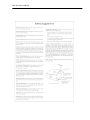
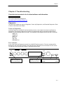
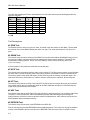
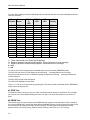
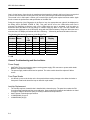
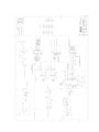
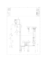
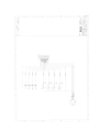
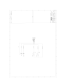
MPX 500
24-Bit Dual Channel
Processor
Service
Manual
MPX 500 Service Manual
Copyright © 1999 Lexicon, Inc.
All Rights Reserved
Lexicon Inc. ● 3 Oak Park ● Bedford, MA 01730-1441 ● Tel (781) 280-0300 ● Customer Service Fax (781) 280-0499
Lexicon Part # 070-14399 Rev 0
Printed in the United States of America
MPX 500 Service Manual
MPX 500 Service Manual
Lexicon
Table of Contents
Chapter 1 Reference Documents, Required Equipment............................. 1-1
Reference Documents............................................................................................................................. 1-1
Required Equipment................................................................................................................................ 1-1
Tools .................................................................................................................................................... 1-1
Test Equipment.................................................................................................................................... 1-1
Chapter 2 General Information ................................................................... 2-1
Periodic Maintenance .............................................................................................................................. 2-1
Ordering Parts ......................................................................................................................................... 2-1
Returning Units to Lexicon for Service .................................................................................................... 2-1
Chapter 3 Specifications............................................................................. 3-1
Chapter 4 Performance Verification............................................................ 4-1
Diagnostics: ............................................................................................................................................. 4-1
Setup: ...................................................................................................................................................... 4-1
I/O Tests: ................................................................................................................................................. 4-1
Analog In To Analog Out Level Test: ................................................................................................... 4-1
Frequency Response Test: ..................................................................................................................... 4-1
Analog In To Analog Out Frequency Test:........................................................................................... 4-1
THD+N Test: ........................................................................................................................................... 4-2
Analog In To Analog Out THD+N Test:................................................................................................ 4-2
Crosstalk Tests:....................................................................................................................................... 4-2
Analog In To Analog Out Crosstalk Test:............................................................................................. 4-2
Dynamic Range Tests: ............................................................................................................................ 4-2
Analog In To Analog Out Dynamic Range Test: .................................................................................. 4-2
Digital I/O Functionality............................................................................................................................ 4-2
MIDI Functionality:................................................................................................................................... 4-3
Footswitch Functionality: ......................................................................................................................... 4-3
Listening Test: ......................................................................................................................................... 4-4
Setup.................................................................................................................................................... 4-4
Verify Clean Audio ............................................................................................................................... 4-4
Shock Test ........................................................................................................................................... 4-4
Lexicon Audio Precision ATE Summary .............................................................................................. 4-5
Chapter 5 Troubleshooting ......................................................................... 5-1
Check the Lexicon web site for the latest software and information:................................................ 5-1
Diagnostics .............................................................................................................................................. 5-1
Power Up Diagnostics.......................................................................................................................... 5-1
Error Indication..................................................................................................................................... 5-1
Test Descriptions ................................................................................................................................. 5-2
#1 ROM Test : .................................................................................................................................. 5-2
#2 SRAM Test: ................................................................................................................................. 5-2
#3 WCS Test: ................................................................................................................................... 5-2
#4 INT Test:...................................................................................................................................... 5-2
#5 ADF Test: .................................................................................................................................... 5-2
#6 EEPROM Test:............................................................................................................................ 5-2
Extended Diagnostics .......................................................................................................................... 5-3
#1 ROM Test : .................................................................................................................................. 5-4
#2 SRAM Test: ................................................................................................................................. 5-4
#3 WCS Test: ................................................................................................................................... 5-5
#4 INT Test:...................................................................................................................................... 5-5
#5 ADF Test: .................................................................................................................................... 5-5
#6 EEPROM Test:............................................................................................................................ 5-5
#7 DRAM Test:................................................................................................................................. 5-5
#8 Switch Test:................................................................................................................................. 5-5
MPX 500 Service Manual
Footswitches: ....................................................................................................................................5-5
Front Panel Switches: .......................................................................................................................5-6
#9 Encoder Test:...............................................................................................................................5-6
#10 MIDI Test:...................................................................................................................................5-7
#11 LCD Test: ...................................................................................................................................5-7
#12 Exit Test: ....................................................................................................................................5-7
#13 Initialize Test: .............................................................................................................................5-7
#14 Unused:......................................................................................................................................5-7
#15 Unused:......................................................................................................................................5-7
#16 Burn In Test:...............................................................................................................................5-7
General Troubleshooting and Service Notes............................................................................................5-8
Power Supply........................................................................................................................................5-8
Front Panel Knobs ................................................................................................................................5-8
Lexichip Replacement ..........................................................................................................................5-8
Chapter 6 Theory of Operation ................................................................... 6-1
Schematic walkthrough ............................................................................................................................6-1
Sheet 1 (INPUT) ...................................................................................................................................6-1
Sheet 2 (DAC) ......................................................................................................................................6-1
Sheet 3 (LEXICHIP3, ROM/RAM, uPROC) ..........................................................................................6-1
Sheet 4 (ENCODERS)..........................................................................................................................6-2
Sheet 5 (MIDI, DIGITAL AUDIO OUT)..................................................................................................6-2
Sheet 6 (DISPLAY DRIVER) ................................................................................................................6-3
Sheet 7 (POWER SUPPLY) .................................................................................................................6-3
Additional Sheets 1 each (SW#1, SW#2) .............................................................................................6-3
Chapter 7 - Parts List.................................................................................. 7-1
Chapter 8 Schematics and Drawings ......................................................... 8-1
Lexicon
Chapter 1 Refe r ence Documents, Required Equipment
Reference Documents
MPX 500 User Guide - Lexicon P/N 070-14116 or latest revision
Required Equipment
Tools
The following is a minimum suggested technician's tool kit required for performing disassembly, assembly
and repairs:
• Clean, antistatic, well lit work area.
• (1) #1 Phillips tip screwdriver
• (1) T9 Torx screwdriver
• (1) 3/16" Hex socket nut driver
• (1) 5/16" Hex socket, full hollow, nut driver with plastic insert (to prevent Front Panel scratches)
• (1) 15mm Hex socket nut driver
• Solder: 63/37 - Tin/Lead Alloy composition, low residue, no-clean solder.
• Magnification glasses and lamps
• SMT Soldering / Desoldering bench-top repair station
Test Equipment
The following is a minimum suggested equipment list required to perform the proof of performance tests.
• Amplifier with speakers or headphones.
• Cables: (dependent on your signal source)
• Audio Input cable (balanced) with shield and a XLR or ¼ “ plug on one end and an
appropriate connector on the opposite end for connection to the Low Distortion Oscillator.
• Audio Output cable (balanced) with shield and a XLR or ¼ “ plug on one end and an
appropriate connector on the opposite end for connection to the Distortion Analyzer.
• (1) MPX 500 Power Cord (choose accordingly):
•
•
•
•
•
•
•
•
•
•
CORD,POWER,NA/IEC,SVT,VW-1,10A, N. AMER
CORD,POWER,IEC, 6A, 2M, EURO
CORD,POWER,IEC, 5A, 2M, UK
CORD,POWER,IEC, 6A, 2M, ITALY
CORD,POWER,IEC, 6A, 2M, SWISS
CORD,POWER,IEC, 6A, 2M, AUSTRALIA
CORD,POWER,IEC, 6A, 2M, JAPAN
CORD,POWER,IEC, 6A, 2M, UNIVERSAL
Lexicon P/N 680-09149
Lexicon P/N 680-08830
Lexicon P/N 680-10093
Lexicon P/N 680-10094
Lexicon P/N 680-10095
Lexicon P/N 680-10096
Lexicon P/N 680-10097
Lexicon P/N 680-10098
•
(1) Low Distortion Oscillator with Single-ended or balanced output , <100 ohms output
impedance, < 0.005% THD.
(1) analog Distortion Analyzer and Level Meter with single-ended or balanced input, switchable
30Hz highpass filter or audio bandpass (20-20kHz) filter
(1) 100 MHz oscilloscope
1-1
Lexicon
Chapter 2 Gene r al Information
Periodic Maintenance
Under normal conditions the MPX 500 requires minimal maintenance. Use a soft, lint-free cloth slightly
dampened with warm water and mild detergent to clean the exterior surfaces of the connector box.
Do not use alcohol, benzene or acetone-based cleaners or any strong commercial cleaners. Avoid
using abrasive materials such as steel wool or metal polish. It the unit is exposed to a dusty environment, a
vacuum or low-pressure blower may be used to remove dust from the unit's exterior.
Ordering Parts
When ordering parts, identify each part by type, price and Lexicon Part Number. Replacement parts can be
ordered from:
LEXICON, INC.
3 Oak Park
Bedford, MA 01730-1441
Telephone: 781-280-0300; Fax: 781-280-0499; email: [email protected]
ATTN: Customer Service
Returning Units to Lexicon for Service
Before returning a unit for warranty or non-warranty service, consult with Lexicon Customer
Service to determine the extent of the problem and to obtain Return Authorization. No equipment
will be accepted without Return Authorization from Lexicon.
If Lexicon recommends that a MPX 500 be returned for repair and you choose to return the unit to Lexicon
for service, Lexicon assumes no responsibility for the unit in shipment from the customer to the factory,
whether the unit is in or out of warranty. All shipments must be well packed (using the original packing
materials if possible), properly insured and consigned, prepaid, to a reliable shipping agent.
When returning a unit for service, please include the following information:
•
•
•
•
•
•
•
•
•
Name
Company Name
Street Address
City, State, Zip Code, Country
Telephone number (including area code and country code where applicable)
Serial Number of the unit
Description of the problem
Preferred method of return shipment
Return Authorization #, on both the inside and outside of the package
Please enclose a brief note describing any conversations with Lexicon personnel (indicate the name of the
person at Lexicon) and give the name and telephone daytime number of the person directly responsible for
maintaining the unit.
Do no include accessories such as manuals, audio cables, footswitches, etc. with the unit, unless
specifically requested to do so by Lexicon Customer Service personnel.
2-1
Lexicon
Chapter 3 Spec i fications
Analog Inputs
Connectors: XLR/TRS balanced
Impedance: 50k balanced; 25kΩ unbalanced
A/D Dynamic Range: 1058dB, typical
Levels: +20 to +8dBu full scale
Resolution: 24-Bit Sigma-Delta Conversion
Analog Outputs
Connectors: XLR/TRS balanced
Impedance: <600Ω
D/A Dynamic Range: 101dB, typical
Levels: +26dBu balanced; +20dBu unbalanced
Resolution: 24-Bit Sigma-Delta Conversion
Frequency Response: 20Hz-20kHz ±1dB
Crosstalk: -96dB @ 1kHz
THD: <0.5%, 20Hz-20kHz
Digital Audio Interface
Connectors: Coaxial RCA; S/PDIF (IEC-958, CP-340)
System Sample Rates
Internal Clock and S/PDIF Input: 44.1kHz, 48kHz
Display: 150 x 32 LCD, Backlit
Footswitch: Tip/Ring/Sleeve phone jack for Bypass and Tap (optional)
MIDI Interface: Connectors: IN, OUT/THRU
System Specifications
Power Requirements: 90-250V 50-60Hz; 12.5W; 3-pin IEC Connector
RFI/ESD: FCC Class B; European EMC Directive 89/336/ECC
Environment: Operating Temperature: 32°-104°F (0°-40°C); Relative Humidity: 95% non-condensing
Dimensions: 19"W x 1.75"H x 5.5"D (483x45x140.25mm)
Weight: 3 lbs (1.4kg)
3-1
Lexicon
Chapter 4 Perfo r mance Verification
This section describes a quick verification of the operation of the MPX 500 and the integrity of its analog
and digital audio signal paths.
Diagnostics:
The MXP 500 contains two types of Diagnostics: Power Up Diagnostics, and Extended Diagnostics. Each
of these will be described fully in Chapter 5: Troubleshooting. When the MPX 500 is powered on, the Power
up Diagnostics run automatically to verify proper operation of its internal systems. The Power Up
Diagnostics consist of the following tests:
ROM Test
SRAM Test
WCS Test
INT Test
ADF Test
EEPROM Test
Setup:
1. Turn on the MPX 500 and wait for the Power Up Diagnostics cycle to finish.
2. Enter System Mode by pressing the System button.
3. Use Edit Knob 1 to select the following System Parameters and Edit Knob 3 to set the parameter as
noted:
3.1. Output Level: 0dB
3.2. Input Source: Analog Stereo
3.3. Clock Source: Internal 44.1k
3.4. Bypass Mode: Dry
4. Press the System button to return to the previous running mode.
5. Turn the Program Select Knob to Program #1.
6. Press the Bypass button on the front panel and verify that the button LED lights.
7. Connect a (balanced) audio cable between the Low Distortion Oscillator and the MPX 500 Left Input.
8. Connect a (balanced) audio cable between the MPX 500 Left output and the Distortion Analyzer.
9. Set the Distortion Analyzer to measure Vrms.
10. Turn the Input Trim knob fully clockwise.
I/O Tests:
These tests will verify the audio performance of the MPX 500's audio input and output circuitry
Analog In To Analog Out Level Test:
1. Apply a 1kHz sinewave signal to the MPX 500 Left Input @ 1.946Vrms.
2. Adjust the Input Trim knob and measure the output for a level between 15.46 and 13.78Vrms.
3. Move the cables to the Right Input/Output connections and repeat step 2.
Frequency Response Test:
These tests will verify the frequency response specifications of the Left and Right analog inputs to the Left
and Right analog output signal paths of the MPX 500.
Analog In To Analog Out Frequency Test:
1. Disable all Filters on the Distortion Analyzer
2. Apply a 1kHz sinewave signal to the MPX 500 Left Input @ 3.083Vrms
4-1
MPX 500 Service Manual
3. Connect the Left Output to the Distortion Analyzer.
4. Set the Analyzer for a 0dB reference (@1kHz).
5. Sweep the Oscillator from 20Hz to 20kHz and verify the level to be within +/- 1.0dBr through out the
sweep.
6. Move the cables to the Right Input/Output connections and repeat step 4 & 5.
THD+N Test:
These tests will verify the THD+N specifications of the MPX 500's Left and Right input to output circuitry.
Analog In To Analog Out THD+N Test:
1.
2.
3.
4.
5.
6.
Apply a 1kHz sinewave signal to the MPX 500 Left Input @ 6.904Vrms.
Connect the Left Output to the Distortion Analyzer.
Set the Distortion Analyzer to measure THD.
Enable the Low pass filters on the Analyzer (30kHz, 20kHz).
Verify the Left output, THD+Noise level on the Analyzer is < 0.005%.
Move the cables to the Right Inputs/Outputs connections and repeat step 5.
Crosstalk Tests:
These tests will verify the crosstalk specifications of the MPX 500's Left and Right input to output circuitry.
Analog In To Analog Out Crosstalk Test:
1.
2.
3.
4.
5.
Apply a 1kHz sinewave signal to the MPX 500 Left Input @ 7.746Vrms.
Connect the Right Output to the Distortion Analyzer.
Enable the Low pass filters on the Analyzer (30kHz, 20kHz).
Sweep the Oscillator from 20Hz to 20kHz and verify the level to be >.245mVrms throughout the sweep.
Move the Input cable to the Right side and the Output cable to the Left and repeat step 4.
Dynamic Range Tests:
These tests will verify the Dynamic Range specifications of the MPX 500's Left and Right input to output
circuitry.
Analog In To Analog Out Dynamic Range Test:
1.
2.
3.
4.
5.
6.
7.
8.
9.
10.
11.
12.
Apply a 1kHz sinewave signal to the MPX 500 Left Input @ 7.746Vrms.
Connect the Left Output to the Distortion Analyzer.
Set the Distortion Analyzer for a 0dB reference
Remove the Input cable from the Left input.
Enable the Low pass filters on the Analyzer (30kHz, 20kHz).
Verify the Noise level at the Left Output is > -97dBr (.218mVrms); (-101 dBr typical).
Connect the 1kHz-sinewave signal to the Right Input of the MPX 500.
Move the Left Output cable to the Right Output.
Set the Distortion Analyzer for a 0dB reference.
Remove the Input cable from the Right input.
Enable the Low pass filters on the Analyzer (30kHz, 20kHz).
Verify the Noise level at the Right Output is > -97dBr (-101 dBr typical).
Repeat Tests @ 48K
Select Internal 48k Clock Source from System mode and repeat all of the above tests.
Digital I/O Functionality
This test will verify that the MPX 500 will pass a valid S/PDIF digital audio signal through its digital input and
output circuitry.
4-2
Lexicon
1. Connect a Digital signal (CD player, DAT, or effects box) to the S/PDIF input jack on the back of the
MPX 500.
2. Connect the S/PDIF output of the MPX 500 to a D/A device (M300) for conversion back to an analog
signal.
3. Connect the analog output of the D/A device (M300) to your amplifier with speaker output. Be sure to
turn the volume down on the amplifier.
4. Turn the volume up on your amplifier to a comfortable listening level and verify audio at the output and
that it is free and clear of any audio defects (pops, clicks, static, etc.).
MIDI Functionality:
This test will verify that the MIDI Input and MIDI Output/Thru circuits are working.
The test will transmit data out of the MIDI OUT jack and will attempt to read the data through the MIDI IN
jack.
Midi functionality is tested through the extended diagnostics of the MPX 500.
To enter the Extended Diagnostics, power on the unit while pressing down & holding the BYPASS button
on the front panel of the MPX 500. When the EDIT LED is lit, the BYPASS button can be released. After it
is released, the EDIT LED will go out and the LCD Display will indicate the first test, # 1 ROM. Turn the
Program Knob CW until test # 10 Midi test is displayed.
Connect a 5 Pin Male DIN to 5 Pin Male DIN Cable (also known as a MIDI cable) between the MIDI IN jack
and the MIDI OUT jack.
Press the Program Knob once to execute the test.
When the test is executed, the LCD Display will indicate the test is “Running…”, followed by the Pass/Fail
status of the test.
To exit the test, press the Program Knob.
Footswitch Functionality:
Footswitch functionality is performed through the extended diagnostics of the MPX 500.
To enter the Extended Diagnostics, power on the unit while pressing down & holding the BYPASS button
on the front panel of the MPX 500. When the EDIT LED is lit the BYPASS button can be released. After it is
released, the EDIT LED will go out and the LCD Display will indicate the first test, # 1 ROM. Turn the
Program Knob CW until test # 8 Switch test is displayed.
To perform this test, a Dual stereo style footswitch must be plugged into the Footswitch jack on the back of
the MPX 500 using a ¼ tip/ring/sleeve cable.
Press the Program Knob once to execute the test.
Press the LEFT FOOTSWITCH (Ring). The BYPASS LED will light and the LCD Display will indicate
“BYPASS”. The remaining LEDs will be off. When the LEFT FOOTSWITCH is released, the BYPASS LED
will go off.
Press the RIGHT FOOTSWITCH (TIP). The TAP LED will light and the LCD Display will indicate “TAP”. The
remaining LEDs will be off. When the RIGHT FOOTSWITCH is released, the TAP LED will go off.
To exit the test, press the Program Knob.
4-3
MPX 500 Service Manual
Listening Test:
Setup
1. Connect an audio cable between the output of the Low Distortion Amplifier and the MPX 500 Left and
Right Inputs.
2. Connect two audio cables between the headphone amplifier inputs and the MPX 500 Left and Right
outputs.
3. Set the headphone amplifier volume control to its lowest level.
4. Set the oscillator for 220Hz sinewave at 100mVrms.
5. Power on the MPX 500 and turn the program knob to the # 1 program Small Plate
Verify Clean Audio
1.
2.
3.
4.
Load Program # 1 Small Plate.
Set the reverb time to 2.04 seconds or greater, the Mix to 100% and Bypass to Off.
Put on headphones and set the headphone amplifier volume to a comfortable listening level.
Sweep the input knob over the entire range and verify that no pops, clicks, distortion, or static noises
are heard when turning the knob.
Shock Test
1. Lift one side of the MPX 500 four inches off the work surface and drop
2. Verify that no audio or display intermittence is caused by this action.
NOTE: To prevent damaging the unit, keep one side of the unit touching the work surface at all times.
4-4
Lexicon
Lexicon Audio Precision ATE Summary
4-5
Lexicon
Chapter 5 Trou b leshooting
Check the Lexicon web site for the latest software and information:
http://www.lexicon.com
The Lexicon Support Knowledgebase:
http://www.lexicon.com/kbase/kbase.asp
Diagnostics
The MXP 500 contains two types of Diagnostics: Power Up Diagnostics, and Extended Diagnostics. Each
of these is described in this chapter.
Power Up Diagnostics
On Normal power up, the MXP 500 will automatically execute a set of tests that comprise the Power Up
Diagnostics. All front panel LEDs will be turned on for approximately 200ms, and then the MPX 500 will
attempt to run the following sequence of tests. The tests have been designed to take less than 10 seconds.
ROM Test
SRAM Test
WCS Test
INT Test
ADF Test
EEPROM Test
Error Indication
If any of the Power Up Diagnostics tests fail, the LOAD LED will be turned on. The error message will be
displayed on the front panel as shown in the example below. This will be true for all tests if an error occurs.
To continue to the next test after a failure is reported press BYPASS.
Edit
Edit
1
2
Program
3
4
Load
Bypass
System
EDIT LED indicates
when test has Passed
LOAD LED indicates
when test has Failed
(MSB)
Store
Tap
(LSB)
5-1
MPX 500 Service Manual
The table below displays the Power Up Diagnostic test code which the front panel will display before the
tests are executed.
Test
No.
1
2
3
4
5
6
Test
Name
ROM
SRAM
WCS
INT
ADF
EEPROM
Bypas
s
0
0
0
1
1
1
Store
Tap
0
1
1
0
0
1
1
0
1
0
1
0
0 = OFF
1 = ON
Test Descriptions
#1 ROM Test :
The ROM checksum, which is a byte size value, is located in the last location of each Bank. The test adds
the contents of the entire ROM including the check sum byte. The result should equal a 0 for the test to
pass.
#2 SRAM Test:
This test will verify the entire contents of the SRAM. The test first writes 00hex (000000000 binary) to all of
the memory locations, and then verifies this by reading back all the memory locations. The test will also
write/read the following patterns: 55hex (01010101 binary), AAhex (10101010 binary), and FFhex
(11111111 binary).
If what is written to all locations is read back, the test will pass.
#3 WCS Test:
This test will verify the program memory space of the Lexichip 3. The Ram (memory space) is first filled with
the value 55hex (01010101 binary), then each memory location is read back to confirm it contains the 55.
The memory space is then filled with AAhex (10101010 binary) and the memory is read back again. The
final test is the memory is filled with 0’s. If what is written to all locations is read back, the test will pass.
#4 INT Test:
This test will verify that the Lexichip 3 interrupt (INT/) is working and occurring at the proper time intervals.
The Lexichip 3 does this by providing this signal to the Z80’s maskable interrupt line. If the Z80 sees the
signal at the proper times the test will pass.
#5 ADF Test:
This test will verify that the Audio Data File in the Lexichip 3 is working properly. The Lexichip 3 Audio Data
File (ADF) is a fast synchronous 128-word SRAM that provides audio data buffering and storage for
external memory references, Serial I/O and the Host-to-Lexichip data port. ADF locations also function as
ARU Registers and as scratchpad memory.
#6 EEPROM Test:
This test will verify the functions of the EEPROM on the MPX 500.
First the test will verify that the EEPROM has been initialized properly. This is done by storing the software
version of the EPROM in the first five bytes of the EEPROM. Then the stored value is verified if correct
5-2
Lexicon
when the test is executed. If the stored value read from the first five bytes of the EEPROM is incorrect, the
EEPROM will be initialized.
Second, the test will read each byte in the User Register portion of the EEPROM and add them together to
calculate a checksum. This value is compared with the checksum value stored in the EEPROM itself. This
checksum will be recalculated each time a register is stored.
Extended Diagnostics
Extended Diagnostics are provided to help in troubleshooting specific functions in the MPX 500.
To enter the Extended Diagnostics, power on the unit while pressing down & holding the BYPASS button
on the front panel of the MPX 500. When the EDIT LED is lit, the BYPASS button can be released. After it
is released, the EDIT LED will go out and the LCD Display will indicate the test number and it name. The
Binary testcode will be displayed on the front panel (Bypass, Store, and Tap LEDs) as was described in the
Power Up Diagnostics section earlier in this chapter.
The following is a complete list of tests in the Extended Diagnostics.
ROM Test
SRAM Test
WCS Test
INT Test
ADF Test
EEPROM Test
DRAM Test
Switch Test
Encoder Test
MIDI Test
LCD Test
Exit Test
Init
Burn In Test
When each of these tests are run, they will display the test code and report an error the same way the
Power Up Diagnostic did. Unlike the power Up diagnostics however, each can be chosen individually by
turning the PROGRAM knob. Once a test is selected, execution of the test is done by pressing the Program
knob.
5-3
MPX 500 Service Manual
The table below displays each Extended Diagnostic test and the code the front panel will display before the
tests are executed:
Test
Number
① 1
① 2
① 3
① 4
① 5
① 6
③ 7
② 8
③ 9
③ 10
② 11
12
13
14
15
③ 16
Test
Name
BYPAS
S
LED
ROM
0
SRAM
0
WCS
0
INT
1
ADF
1
EEPROM
1
DRAM
1
Switch
0
Encoder
0
MIDI
0
LCD
0
Exit
0
Init
0
Unused
0
Unused
0
Burn In
0
STORE
LED
TAP
LED
LCD
Display
0
1
1
0
0
1
1
0
0
0
0
0
0
0
0
0
1
0
1
0
1
0
1
0
0
0
0
0
0
0
0
0
ROM
SRAM
WCS
INT
ADF
EEPROM
DRAM
Switch
Encode
MIDI
LCD
Exit
Init
Unused
Unused
BurnIn
① These tests reside in the Power Up Diagnostics.
② Requires operator interaction and judgment. Doesn't generate an error message.
③ Requires operator interaction and judgment. Generates an error message.
0 = OFF
1 = ON
To execute each of the following tests, the BANK button must be pressed (PROGRAM knob).
The lower left side of the LCD will display the word Running … indicating that the test is working.
After the test has run its course, a Pass/Fail message will replace the Running… message indicating the
results of the test.
The EDIT LED will light if the test Passes.
The LOAD LED will light if the test Fails.
Tests 1 to 11 can be run continuously by pressing the TAP button instead of the BANK button (PROGRAM
knob) when executing the test.
#1 ROM Test :
The ROM checksum, which is a byte size value is located in the last location of each Bank. The test adds
the contents of the entire ROM including the check sum byte. The result should equal a 0 for the test to
pass.
#2 SRAM Test:
This test will verify the entire contents of the SRAM with the exception of the stack area which is tested by
the power-up SRAM test. The test first writes 00hex (000000000 binary) to all of the memory locations, and
then verifies this by reading back all the memory locations. The test will also write/read the following
patterns: 55hex (01010101 binary), AAhex (10101010 binary), and FFhex (11111111 binary).
5-4
Lexicon
If what is written to all locations is read back, the test will pass.
#3 WCS Test:
This test will verify the program memory space of the Lexichip 3. The Ram (memory space) is first filled with
the value 55hex (01010101 binary), then each memory location is read back to confirm it contains the 55.
The memory space is then filled with AAhex (10101010 binary) and the memory is read back again. The
final test is the memory is filled with 0s. If what is written to all locations is read back, the test will pass.
#4 INT Test:
This test will verify that the Lexichip 3 interrupt (INT/) is working and occurring at the proper time intervals.
The Lexichip 3 does this by providing this signal to the Z80’s maskable interrupt line. If the Z80 sees the
signal at the proper times the test will pass.
#5 ADF Test:
This test will verify that the Audio Data File in the Lexichip 3 is working properly. The Lexichip 3 Audio Data
File (ADF) is a fast synchronous 128-word SRAM that provides audio data buffering and storage for
external memory references, Serial I/O and the Host-to-Lexichip data port. ADF locations also function as
ARU Registers and as scratchpad memory.
#6 EEPROM Test:
This test has 2 parts that will verify the functions of the EEPROM in the MPX 500. The EEPROM will be
initialized if either of the two parts of the test fail.
The First part of the test will read each byte in the User Register portion of the EEPROM and add them
together to calculate a checksum. This value is compared with the checksum value stored in the EEPROM
itself. This checksum will be recalculated each time a register is stored.
The Second part of the test will verify that the EEPROM has been initialized properly. This is done by
storing the software version of the EPROM in the first five bytes of the EEPROM. Then the stored value is
verified when the test is executed. If the stored value read from the first five bytes of the EEPROM is
incorrect, the EEPROM will be initialized.
#7 DRAM Test:
The Z80 performs two tests to verify the DRAM, a Data test and an Address test.
In the Data test, the Z80 writes AA (hex) (10101010) into all of the memory locations then reads them back
to check them. It repeats the process with 55 (01010101).
The Address test, the Z80 writes a count into the memory then reads it back (i.e. 00000001, 00000010,
00000011). This test will take approximately 45 seconds to complete.
#8 Switch Test:
The Switch Test diagnostics has two tests. The tests verify the operation of the Front panel switches (7)
and Footswitches (2) along with their associated LEDs at the same time. The LCD Display will also indicate
the name of the switch being pressed & held.
Footswitches:
To perform this test, a Dual stereo style footswitch must be plugged into the Footswitch jack on the back of
the MPX 500 using a ¼” tip/ring/sleeve cable.
Press the LEFT FOOTSWITCH (Ring). The BYPASS LED will light and the LCD Display will indicate
5-5
MPX 500 Service Manual
“BYPASS”. The remaining LEDs will be off. When the LEFT FOOTSWITCH is released, the BYPASS LED
will go off.
Press the RIGHT FOOTSWITCH (TIP). The TAP LED will light and the LCD Display will indicate “TAP”. The
remaining LEDs will be off. When the RIGHT FOOTSWITCH is released, the TAP LED will go off.
Front Panel Switches:
Press and hold the EDIT button. The EDIT LED will light, and the LCD Display will indicate “EDIT”. The
remaining LEDs will be off. When the EDIT button is released, the EDIT LED will be turned off.
Press and hold the SYSTEM button. The SYSTEM LED will light, and the LCD Display will indicate
“SYSTEM”. The remaining LEDs will be off. When the SYSTEM button is released, the SYSTEM LED will
be turned off.
Press and hold the LOAD button. The LOAD LED will light, and the LCD Display will indicate “LOAD”. The
remaining LEDs will be off. When the LOAD button is released, the LOAD LED will be turned off.
Press and hold the BYPASS button. The BYPASS LED will light, and the LCD Display will indicate
“BYPASS”. The remaining LEDs will be off. When the BYPASS button is released, the BYPASS LED will
be turned off.
Press and hold the STORE button. The STORE LED will light, and the LCD Display will indicate “STORE”.
The remaining LEDs will be off. When the STORE button is released, the STORE LED will be turned off.
Press and hold the TAP button. The TAP LED will light, and the LCD Display will indicate “TAP”. The
remaining LEDs will be off. When the TAP button is released, the TAP LED will be turned off.
Press and hold the BANK button (PROGRAM knob). The LCD Display will indicate “BANK”. The remaining
LEDs will be off. When the BANK button (PROGRAM knob) is released, the LCD Display will indicate
“Done”.
#9 Encoder Test:
During this test, the Z80 microprocessor reads the value of the encoder being tested and then expects the
next value read from the encoder (when the encoder position is moved) will be at a predetermined
incremental value. Therefore, during the test each encoder must be rotated in a clockwise direction as it is
being tested, or the test will fail.
When the test is executed, all front panel LEDs will be turned off and the LCD Display will indicate the
encoder that is under test along with the hexadecimal value of the encoder’s current position. The
hexadecimal values range from (0-F) for the EDIT (1-4) encoders and from (00-1F) for the PROGRAM
encoder. The encoders are tested in the following sequence: EDIT 1, EDIT 2, EDIT 3, EDIT 4 and
PROGRAM.
When the test is executed, the LCD Display will indicate in the lower left corner the encoder under test
(EDIT 1 -- XX) along with the hexadecimal value of the encoder’s current position.
Turn the EDIT 1 encoder Clockwise (CW) one revolution (16 positions). The LCD Display will momentarily
indicate the Pass/Fail status (i.e. EDIT 1 – PASS). Confirm and proceed to test the next encoder.
5-6
Lexicon
Turn the EDIT 2 encoder Clockwise (CW) one revolution (16 positions). The LCD Display will momentarily
indicate the Pass/Fail status (i.e. EDIT 2 – PASS). Confirm and proceed to test the next encoder.
Turn the EDIT 3 encoder Clockwise (CW) one revolution (16 positions). The LCD Display will momentarily
indicate the Pass/Fail status (i.e. EDIT 3 – PASS). Confirm and proceed to test the next encoder.
Turn the EDIT 4 encoder Clockwise (CW) one revolution (16 positions). The LCD Display will momentarily
indicate the Pass/Fail status (i.e. EDIT 4 – PASS). Confirm and proceed to test the next encoder.
Turn the PROGRAM encoder Clockwise (CW) one and one half revolutions (32 positions). The LCD
Display will indicate the Pass/Fail status (i.e. PROGRAM – PASS).
Pressing the BANK button (PROGRAM knob) will exit the test. The LCD Display will momentarily indicate
“Done”, then return to the Extended Diagnostics.
#10 MIDI Test:
This test will verify that the MIDI Input and MIDI Output/Thru circuits are working. The test will transmit data
out of the MIDI OUT jack and will attempt to read the data through the MIDI IN jack.
To run this test, a 5 Pin Male DIN to 5 Pin Male DIN Cable (also known as a MIDI cable) must be connected
between the MIDI IN jack and the MIDI OUT jack.
When the test is executed, the LCD Display will indicate the test is “Running…” followed by the Pass/Fail
status of the test.
#11 LCD Test:
This test will verify all the elements of the display are working properly.
When the test is executed, the LCD Display will indicate the test is “Running…” and the LCD Display is
filled with 3 random patterns until all of the pixels have turned black on the LCD Display.
Press and hold the BANK button (PROGRAM knob). This will clear all of the pixels on the LCD Display.
Releasing the BANK button will exit the test.
The LCD Display will indicate “Done”.
#12 Exit Test:
This selection will allow the user to exit the Extended Diagnostic Mode and enter normal operating mode.
Pressing the BANK button (PROGRAM knob) will execute the test.
#13 Initialize Test:
This test will initialize all of the MPX 500 system parameters to their factory default settings.
Pressing the BANK button (PROGRAM knob) will execute the test.
WARNING: This procedure will destroy any user settings or registers.
#14 Unused:
#15 Unused:
#16 Burn In Test:
The Burn In test is structured to help in two ways.
5-7
MPX 500 Service Manual
One is for the factory. Once the unit is manufactured and tested it is placed in this burn in loop over a period
of time to exercise the main circuitry and verify the unit is performing to manufactured specifications.
The second is for in field repair. It allows you to exercise the circuitry after repairs have been made. Again
this is to insure the performance and specification of the MPX 500.
During the execution of the Diagnostics in the Burn In loop, the appropriate test code will be displayed on
the Binary LED’s (BYPASS, STORE & TAP). This code will be sent to the LEDs before each test is
executed. By displaying a test/error code on the LEDs before the test is activated, it will be easier to
determine which test failed if the unit hangs or crashes during the Burn In loop. The test numbers and
names are also displayed on the LCD Display, along with the Pass/Fail status of each test. When the test is
executed, the LCD Display will indicate the test is “Running…” followed by the Pass/Fail status of the test.
The following table shows the tests run in the Burn In Test.
Test
Number
Test
Name
1
2
3
4
5
7
ROM
SRAM
WCS
INT
ADF
DRAM
Bypas
s
LED
0
0
0
1
1
1
Store
LED
Tap
LED
0
1
1
0
0
1
1
0
1
0
1
1
LCD
Display
ROM
SRAM
WCS
INT
ADF
DRAM
0 = OFF
1 = ON
General Troubleshooting and Service Notes
Power Supply
•
•
CAUTION: There is no protective paper covering power supply, IEC connector or power switch leads.
Beware of exposed line voltages.
The power supply module should not be repaired. The entire module should be replaced if failure
occurs.
Front Panel Knobs
•
It is difficult to remove the knobs on the front panel without causing damage to the either the knobs or
front panel. Extra knobs should be kept on hand for repair needs.
Lexichip Replacement
•
•
•
•
5-8
The Lexichip requires a heatsink that is installed with a thermal epoxy. The parts list contains the P/N
for replacement heatsinks and the proper adhesive. Keep replacement heatsinks and adhesive on hand
for repairs. Adhesive should be epoxy, thermally-conductive and equivalent to:
Aavid Thermal Technologies part number
161000F00000 (10 gm) or
164000F00000 (40 gm)
Lexicon
Chapter 6 Theo r y of Operation
Schematic walkthrough
Sheet 1 (INPUT)
This sheet shows the input jacks, input amplifier (U12, U24) and A/D converter (U17) and their associated
circuits.
The MPX500 is fitted with both ¼” balanced phone and XLR input connectors for left and right input signals.
Inserting the ¼” phone plug on J11 or J12 will disconnect signals from XLR jack J10 and J13 respectively.
The following analog circuit description applies to the left signal channel; the function of the corresponding
components in the right channel is identical. Capacitors C42 and C43, along with ferrite beads FB10 and
FB11, prevent unwanted high frequency interference from entering of leaving through the input cables. DC
blocking is achieved by capacitors C74 and C79 in line with each leg of balanced signal path. R71, R72,
R74 and R75 along with C73 and C78 form a 6dB attenuator with a low-pass characteristic. Single stage
input amplifier U12 buffers the attenuated input and supplies gain, which is variable from about +9 to
+23dB, according to the setting of front-panel input trim control R149. The amplifier stage tends to balance
an unbalanced input, more so when operated at the higher gain needed for low level, unbalanced signal
sources. The differential signal from the amplifier is attenuated by R65-R68, ac coupled by C70 and C71,
and biased to 2.5VDC through R62 and R63. The bias voltage is developed from +5VA by the voltage
divider formed by R61 and R64, filtered by C68 and C69. The amplifier output is attenuated by about 18dB
to drive the differential input of the A/D converter, which has a full-scale sensitivity of about +7dBu. The
14dB trim range varies the resulting full-scale input sensitivity from around +6dBV to +22dBu. Capacitors
C92 and C98 at the converter input serve to reduce ailing of spectral components at the 5 to 6MHz
oversampling frequency. The AK5383 (U17) is a 24bit, 128X over sampling 2 channel A/D converter
configured to produce serial digital audio in I2S format.
For information on the AK5383 see http://www.akm.com/AKM/AKMprodinfo.htm
Sheet 2 (DAC)
This sheet shows the analog D/A converter (U11), filter and driver (U7, U8) and their associated circuits.
The 24 bit, 2 channel D/A converter CS4390 is configured to accept serial digital audio in I2S format. The
following analog circuit description is for the left channel; the function of the corresponding components in
the right channel is identical. The output of the converter feeds a differential multiple-feedback 2-pole lowpass filter having a gain of about +12dB, formed by one section of dual op-amp U7 and associated
components. The other section of U7 inverts the single-ended filtered signal. The two outputs of U7 drive
the balanced output through series resistors R35 and R33, which isolate the amplifiers from capacitive
loads and present a differential output impedance of around 600 ohms. Output is available simultaneously
on the parallel-wired XLR and ¼” phone jack connectors, J6 and J7. If unbalanced output wiring is used
which grounds the ring of J7, R33 limits the current. Full-scale differential output from the converter is
2Vrms, or about +8dBu, which results in a full-scale output level of +26dBu balanced, +20dBu unbalanced.
Capacitors C24 and C26, along with ferrite beads FB6 and FB7, prevent unwanted high frequency
interference from entering or leaving through the output cables.
For information on CS4390 see http://www.cirrus.com/products/overviews/cs4380.html
Product data sheet (PDF) http://www.cirrus.com/ftp/pubs/4390.pdf
Sheet 3 (LEXICHIP3, ROM/RAM, uPROC)
This sheet shows the Z80 microprocessor (U13), EPROM (U9), EEPROM (U5), SRAM (U2), Audio DRAM
(U6) and digital signal processor Lexichip3 (U10) and their associated circuits.
6-1
MPX 500 Service Manual
The configuration resistors R115-R122 on system data bus are used to program the Lexichip3 operating
mode. Upon the rising edge of RESET/, various Lexichip3 mode bits are set which determines the system
operating parameters. If any chip on the Z80 data bus erroneously drives the data bus during RESET/, the
Lexichip3 will come up in the wrong mode and the Z80 will not function properly. Therefore, during
RESET/, all the relevant chip enables must be pulled high and the Z80 must be fed clocks to allow the
resistors to work as designed. Proper initialization of the system is dependent on the static state of the data
bus on power up which is provided by R115-122 and on the default state of other lines governed by R10,
R17, R23-24, R80-81, R54-56, R95, R76, R114. Be sure to check these and clocks if the system will not
come up.
The Z80 (U13) handles all basic system control and user interface I/O operation. Normally, the Z80 clock
ZCLK is derived from the Lexichip3 M_ZCLK pin, via GAL U20 (sheet 5). However, when RESET/ is
asserted, before the Lexichip3 is functioning, the GAL feeds ZCLK from the 12.288MHz crystal oscillator.
The Lexichip3 master clock (CLK_IN, pin 75), is driven by 256FS48, from the 12.288MHz crystal oscillator
(sheet 5). All the system software and programs are stored in 256Kx8 EPROM (U9). The Z80’s memory is
a 32Kx8 SRAM (U2). User programs are stored in a 4kx8 EEPROM (U5). The EEPROM clock is driven by
the Lexichip3 under program control. The serial data line (EEPROM_DATA) is bi-directional. R22 prevents
excessive current in either the EEPROM or the Lexichip3 during power-up, when both chips might drive the
line. The audio memory for the Lexichip3 is provided by 1Mx4 DRAM (U6). Note that all address decoding
(RAM_EN/, ROM_EN/, etc.) is done within the Lexichip3. That is the primary reason the Z80 cannot
function if the Lexichip3 is improperly initialized at the rising edge of RESET/.
Sheet 4 (ENCODERS)
This sheet shows the front panel PROGRAM EDIT encoders and their associated circuits.
Four-bit gray-code encoders SW1-SW4 are multiplexed two at a time onto a shared 8-bit bus, ENC [7-0],
which is readable by software. Pull-up resistors R124-R131 default the bus to logic high.
Diodes D12-D15 (Program Edit 4 encoder), D16-D19 (Program Edit 3 encoder), D20-D23 (Program Edit 2
encoder), D24-D27 (Program Edit 1 encoder) are used to isolate the output of the unselected encoder pair
during the reading of the selected encoder pair. An encoder is selected when its C pin is set low, which
allows the encoder to assert its current position onto the ENC bus via the corresponding group of diodes.
The C pin is controlled via Lexichip3 (sheet 3) PIO bits. In addition to the encoders, the closure of the
individual front panel switches associated with D5, D6, D28, D29, D7, D8 and D9 can be read when
SWITCH_SELECT/ (sheet 6, A5) is asserted. Software selects which set of signals is placed on the ENC
bus by asserting ADJ12_SELECT/, ADJ34_SELECT/, or SWITCH_SELECT/. The state of the ENC bus is
then read via the 74HC541 (U23).
Sheet 5 (MIDI, DIGITAL AUDIO OUT)
This sheet shows the Clock generation, MIDI I/O and S/PDIF I/O and their associated circuits.
At the center of the sheet are the crystal oscillators, which are the basis for the two sample rate clocks (44.1
kHz and 48 kHz). These clocks, 256FS441 and 256FS48M, plus 256FSPLL, from the digital audio
receiver, are fed to 74HC153 (U15) where they are software selected via CLK_SEL0 and CLK_SEL1. A
GAL16V8R-25 (U10) provides various clocks and control signals including ZRST/ to the Z80. The
Lexichip3 is clocked by 256FS48, and is set to execute 255 instructions out of a possible 256. This means
that it will execute DSP operations properly at 48 kHz + ca. 0.4% (1/256).
The MPX500 MIDI interface complies with the MIDI specification. It incorporates 5-pin female DIN
connectors for input, thru and out (J2 and J3). J3 is shared for thu and out, according to how the Lexichip3
is programmed. MIDI INPUT is opto-coupled for ground isolation through U1 to the MIDI UART within the
Lexichip3 (sheet 3). The MIDI OUTPUT signal is generated by the Lexichip3 (sheet 3) and is fed to current
loop driver Q1 and out J3. FB1-2 and J2-3 shields connection to ground are to reduce RFI.
6-2
Lexicon
The S/PDIF OUT is generated by the Lexichip3 (sheet 3) and buffered by two gate sections of U3
(74HC132). The voltage divider formed by R13-R15 develops an open-circuit voltage at J5 of 1Vp-p, accoupled by C8 and C9. Output impedance is about 75Ω, which produces the standard 500mVp-p S/PDIF
signal when connected to a 75Ω terminated load. The S/PDIF OUT is gated with RESET/ to mute the digital
output.
S/PDIF IN connected to J5 is terminated in 75Ω by R18, ac-coupled by C13, and amplified by U4
(74HCU04). Current limiting resistor R19 and clamping diode D3 provide input protection. The amplified
signal is demodulated by digital audio receiver CS8412 (U14), which delivers a serial stream in I2S format
to the Lexichip3. The signals C0/, CA, CB, CC, CD, CE and ERF allow software to determine the lock,
error status, and sample rate detected by U14. CK_6MHZ provides a reference clock used by U14 to
determine incoming sample rate.
For information on CS8412 http://www.cirrus.com/products/overviews
Product data sheet (PDF) http://www.cirrus.com/ftp/pubs
Sheet 6 (DISPLAY DRIVER)
This sheet shows the footswitch jack, LCD connection, LCD contrast, led driver, SW #1 and SW#2
connections and their associated circuits.
The tip and ring of the footswitch ¼” phone jack (J4) connect to FOOT_TAP/ and FOOT_BYPASS/,
respectively, through current-limiting resistors R11 and R12. Capacitors C5 and C6 filter out RFI. D10 and
D11 help protect from over voltage or static discharge. Pull-up resistors R100 and R101 default the nonactive switch state to logic high. FOOT_TAP/ and FOOT_BYPASS/ are fed to 74HC541 (U19), which allows
software to determine the footswitch state.
Signals ENCA and ENCB are from the two-phase incremental rotary encoder on the SW1 board. The
encoder bits are pulled-up by R86 and R87 and filtered by R85, R88, C102 and C103. Software determines
the state of the encoder by reading U19.
Connector (J19) is the interface to the front-panel LCD module. R102-112 are series damping resistors for
the LCD address, control and data lines. 10K-potentiometer (R2) adjusts the LCD contrast. The front-panel
LED’s on the SW#1 and SW#2 boards are controlled by software via U18 (74AC273) and associated
current-limiting resistors.
For information on LCD (PDF) ftp://wfp62508.w1.com/s150gs32.pdf.
Sheet 7 (POWER SUPPLY)
This sheet shows the power supply, reset generator and their associated circuits.
The Reset generator is formed by two sections of U3 (74HC132), along with C11 (22uF) and R16 (1K).
RESET/ is held low during initialization, immediately after power is applied.
Main power is applied to IEC connector (J1). The MPX500 incorporates a switching power supply module,
which accepts main voltages from 90-240V AC. The power switch on front panel is in series with the main
input to the power supply module. The supply delivers +/-15VDC and +5VDC, which is conditioned by
capacitors, resistor and chokes shown.
Additional Sheets 1 each (SW#1, SW#2)
SW#1 incorporates (4) LED’s, (4) switches, and encoder SW5, which connect to the MAIN board via J18.
SW5 is a 24-position rotary encoder, which includes a push-action switch, used to access the bank function
in system.
SW#2 incorporates (2) LED’s and (2) switches, wired to the MAIN board via J20.
6-3
Lexicon
Chapter 7 - Pa r ts List
MPX500 MAIN BOARD ASSEMBLY
PART NO.
120-14142
200-14153
200-14157
202-09794
202-09795
202-09871
202-09873
DESCRIPTION
QTY
ADHESIVE,EPOXY,THERMAL
POT,RTY,10KB,KNURL,6MMX15MML 1.00
POT,RTY,10K15CX2,7MMFL,14,15L 1.00
RESSM,RO,0 OHM,0805
4.00
RESSM,RO,5%,1/10W,2.2K OHM
5.00
RESSM,RO,5%,1/10W,1K OHM
2.00
RESSM,RO,5%,1/10W,10K OHM
29.00
202-09899
202-10557
202-10558
RESSM,RO,5%,1/10W,47 OHM
RESSM,RO,5%,1/10W,4.7K OHM
RESSM,RO,5%,1/10W,47K OHM
15.00
2.00
12.00
202-10559
202-10569
202-10574
202-10586
202-10891
202-11041
202-11071
202-11072
202-11073
202-11347
202-11683
203-10583
RESSM,RO,5%,1/10W,100 OHM
RESSM,RO,5%,1/10W,10 OHM
RESSM,RO,5%,1/10W,10M OHM
RESSM,RO,5%,1/4W,100 OHM
RESSM,RO,5%,1/10W,270 OHM
RESSM,RO,5%,1/10W,680 OHM
RESSM,RO,5%,1/4W,75 OHM
RESSM,RO,5%,1/4W,220 0HM
RESSM,RO,5%,1/4W,270 OHM
RESSM,RO,5%,1/4W,3 OHM
RESSM,RO,5%,1/10W,5.1 OHM
RESSM,RO,1%,1/10W,10.0K OHM
3.00
1.00
2.00
1.00
6.00
1.00
1.00
3.00
5.00
1.00
1.00
16.00
203-10896
RESSM,RO,1%,1/10W,1.00K OHM
8.00
203-11075
203-11079
203-11723
203-11992
203-12481
203-12837
RESSM,RO,1%,1/10W,95.3 OHM
RESSM,RO,1%,1/10W,715 OHM
RESSM,RO,1%,1/10W,4.75K OHM
RESSM,RO,1%,1/10W,174 OHM
RESSM,RO,1%,1/10W,1.5K OHM
RESSM,RO,1%,1/10W,13.0K OHM
1.00
2.00
4.00
4.00
2.00
8.00
203-12841
240-01262
240-09367
240-09786
240-11827
RESSM,RO,1%,1/10W,39.2K OHM
4.00
CAP,ELEC,330uF,25V,20%,RAD
1.00
CAPSM,ELEC,10uF,25V,NONPOL,20%4.00
CAP,ELEC,100uF,25V,RAD,LOW ESR 3.00
CAPSM,ELEC,10uF,16V,20%
7.00
240-13216
240-13217
241-09798
244-10423
244-12322
245-09876
245-10561
245-10562
CAPSM,ELEC,22uF,16V,20%
CAPSM,ELEC,47uF,16V,20%
CAPSM,TANT,10uF,10V,20%
CAP,MYL,.22UF,10%,RAD
CAP,MYL,.047uF,50V,RAD,5%,BOX
CAPSM,CER,.01uF,50V,Z5U,20%
CAPSM,CER,100pF,50V,COG,5%
CAPSM,CER,150pF,50V,COG,10%
1.00
4.00
3.00
5.00
1.00
6.00
2.00
15.00
REFERENCE
Lexichip Heatsink
R2
R149
R28,30-32
R9,20,96-98
R16,78
R1,10,17,23,24,29
R54-56,58,76,79-81
85-88,95,99,114-122
R25-27,77,102-112
R11,12
R21,83,100,101
R124-131
R19,57,84
R59
R82,123
R53
R89-92,132,133
R22
R18
R5,7,8
R6,33,35,43,45
R113
R60
R34,36,41,42,44,46
R51,52,61,64,70,73
R134,137,143,146
R62,63,66,68,135
R136,139,141
R15
R13,14
R38,39,48,49
R65,67,138,140
R69,142
R71,72,74,75,144
R145,147,148
R37,40,47,50
C53
C74,79,119,124
C16,17,50
C63,69,90,95,96
C101,114
C11
C70,71,115,116
C65,67,85
C20,22,47,49,52
C83
C8,13,62,81,102,103
C2,3
C5,6,19,21,24,26
7-1
MPX 500 Service Manual
PART NO.
245-10587
245-10976
245-11594
245-11625
DESCRIPTION
CAPSM,CER,18pF,50V,COG,10%
CAPSM,CER,47pF,50V,COG,5%
CAPSM,CER,2200pF,50V,COG,5%
CAPSM,CER,33pF,50V,COG,5%
245-11626
245-11899
245-12485
CAPSM,CER,75pF,50V,COG,5%
CAPSM,CER,820pF,50V,COG,5%
CAPSM,CER,.1uF,25V,Z5U,20%
270-06671
270-11545
300-10509
300-10563
310-10510
330-10523
330-10528
330-10535
330-10537
330-11990
330-12844
340-11573
345-12060
350-12384
350-13863
350-14158
350-14175
350-14176
355-12333
355-13829
365-09883
375-12110
390-12361
390-12362
452-11947
510-07888
510-09790
510-10881
510-11087
510-13149
510-14156
510-14159
520-09736
620-12428
635-05689
640-01706
640-04339
643-01732
650-03970
675-08256
FERRITE CHOKE,2.5 TURN
3.00
FERRITESM,CHIP,600 OHM,0805
16.00
DIODESM,1N914,SOT23
26.00
DIODESM,DUAL,SERIES,GP,SOT23 3.00
TRANSISTORSM,2N3904,SOT23
1.00
ICSM,DIGITAL,74HCU04,SOIC
3.00
ICSM,DIGITAL,74HC153,SOIC
1.00
ICSM,DIGITAL,74AC273,SOIC
1.00
ICSM,DIGITAL,74HC541,SOIC
3.00
ICSM,LEXICHIP3B,100PIN,PQFP
1.00
ICSM,DIGITAL,74HC132,SOIC
1.00
ICSM,LIN,NJM4580,DUALOPAMP,SOP4.00
ICSM,INTER,CS8412,RCVR,SOIC
1.00
ICSM,DRAM,1MX4,60NS,SOJ
1.00
ICSM,SRAM,32KX8,70NS,SOIC,20uA 1.00
ICSM,EEPROM,24C32,32K,SER,SOIC 1.00
IC,ROM,27C020,MPX500,V1.04
1.00
ICSM,GAL,16V8,MPX500,V1.00
1.00
ICSM,DAC,CS4390,24BIT,STR,SSOP 1.00
ICSM,ADC,AKM5383,24b,96kHz,SOP 1.00
ICSM,uPROC,Z80,CMOS,10MHz,QFP 1.00
ICSM,OPTO-ISOL,HCPL0601,SOIC
1.00
CRYSTALSM,11.2896MHz,PAR,HC49 1.00
CRYSTALSM,12.288MHz,PAR,HC49 1.00
SW,RTY,ENC,16POS,4BIT,15.5L
4.00
CONN,AC,3MC,PCRA,IEC,10A
1.00
CONN,DIN,5FC@180DEG,PCRA,SHLD2.00
CONN,XLR,3MC,PCRA,PLASTIC CMPT2.00
1/4"PH JACK,PCRA,3C,SW-TR,G,FT 5.00
CONN,RCA,PCRA,1FCGX2V,WH/RED,G
CONN,FFC,1.25MM,22POS,PCRA
1.00
CONN,XLR,3FC,PCRA,NO LATCH,SM 2.00
IC,SCKT,32 PIN,PC,TIN,LO-PRO
1.00
LUG,#4,INT STAR,XLR GND
2.00
FASTNR,SWAGE,PCB,4-40X.065,SS 4.00
SCRW,4-40X3/8,PNH,PH,ZN
2.00
SCRW,4-40X1/4,PNH,PH,SEMS,ZN
4.00
NUT,4-40,KEP,ZN
2.00
POPRVT,1/8X1/8,REG PROT HD,SS 1.00
WIRE,22G,BLU,2.5",.187QDC/ST
1.00
7-2
QTY
2.00
6.00
2.00
8.00
4.00
4.00
45.00
C33,35,42-46,48,51
REFERENCE
C25,34
C7,12,73,78,118,123
C92,98
C72,77,87,88,109
C110,117,122
C29,30,38,39
C31,32,40,41
C1,4,9,10,14,15,18
C23,27,28,36,37
C54-61,64,66,68,75
C76,80,82,84,86,89
C91,93,94,97,99,100
C104-108,112,113
C120,121
FB3-5
FB1,2,6-19
D1,2,4-9,12-29
D3,10,11
Q1
U4,16,22
U15
U18
U19,21,23
U10
U3
U7,8,12,24
U14
U6
U2
U5
U9
U20
U11
U17
U13
U1
Y1
Y2
SW1-4
J1
J2,3
J6,9
J4,7,8,11,12
1.00
J5
J19
J10,13
U9
J6,9
PS TO MAIN BD
AC CONN (J1)
PS TO MAIN BD
AC CONN (J1)
BRKT TO MAIN BD
J17
Lexicon
675-08257
PART NO.
675-14137
680-14173
680-14174
701-14147
704-14132
710-14120
750-14151
WIRE,22G,BRN,2.5",.187QDC/ST
DESCRIPTION
WIRE,18G,GRN/YEL,7",#6RING/SS
CABLE,.156,HSG/ST&T,4C,3"
CABLE,.100,HSG/ST&T,2C,3"
BRACKET,KEYSTONE,633,.140DX2
HEATSINK,TO220,.75X.5X.5"H
PC BD,MAIN,MPX500
PWR SUP,+5V/+15V/-15V,16.5W
1.00
QTY
1.00
1.00
1.00
1.00
1.00
1.00
1.00
J16
REFERENCE
AC CONN (J1) TO FP
J15
J14
MAIN BD MTG
U10
QTY
4.00
1.00
4.00
4.00
1.00
1.00
REFERENCE
D1-4
SW5
SW1-4
D1-4
J1
QTY
2.00
2.00
2.00
1.00
1.00
REFERENCE
D1,2
SW1,2
D1,2
J1
PART NO.
430-14152
454-11095
550-11929
550-11931
550-14168
550-14169
630-14114
635-12831
640-02812
DESCRIPTION
QTY
DISP,LCD,150X32DOTS,12:00,FFC
1.00
SW,ROCKER,1P2T,6A@250,VERTSLIM1.00
KNOB,.69D,6MM/FL,BLK,LINE
1.00
BUTTON,.24X.64,BLK,W/LT PIPE
6.00
KNOB,.85D,6MM/FL,BLK
4.00
KNOB,1.05D,6MM/FL,BLK
1.00
SPCR,4-40X7/16,3/16HEX,NYL
2.00
SPCR,.14IDX.25ODX.375L,AL
4.00
SCRW,4-40X3/8,PNH,PH,BLK
7.00
REFERENCE
640-14115
641-11466
641-12759
643-01732
SCRW,4-40X3/16,PNH,PH,NYL
SCRW,TAP,#4X3/8,PNH,PH,BZ,TRI
SCRW,TAP,AB,#2X1/4,PNH,PH,BZ
NUT,4-40,KEP,ZN
2.00
9.00
4.00
6.00
700-14164
702-14160
702-14163
702-14177
703-14167
COVER,MPX500
PANEL,FRONT,MPX500
PANEL,SIDE,1.71X5.42
COVER,PROTECTIVE,PS,4.10X4.10
LENS,3.37X.87,CLR
1.00
1.00
2.00
2.00
1.00
MPX500 SW#1 BOARD ASSEMBLY
PART NO.
430-07326
452-14155
453-12166
630-14190
680-14171
710-14130
DESCRIPTION
LED,GRN,T1,LITON
SW,RTY,ENC,24POS,12MM,PBM
SW,PBM,1P1T,6MMSQ,250GF
SPCR,LED,T1,2MMH
CABLE,RIB,24-26AWG,14CX.1,3"L
PC BD,SW#1,MPX500
MPX500 SW#2 BOARD ASSEMBLY
PART NO.
430-07326
453-12166
630-14190
680-14170
710-14140
DESCRIPTION
LED,GRN,T1,LITON
SW,PBM,1P1T,6MMSQ,250GF
SPCR,LED,T1,2MMH
CABLE,RIB,24-26AWG,6CX.1,3"L
PC BD,SW#2,MPX500
MPX500 MECHANICAL ASSEMBLY
DISPLAY
SW BDS TO FP
COVER TO FP & SIDE PANELS
AC CONN
DISPLAY
XLR & RCA CONN
DIN CONN
SW BDS TO FP (4);
KEYSTONE TO FP (1);
AC CONN (1)
COVER, INSIDE
7-3
MPX 500 Service Manual
740-08558
PART NO.
740-09538
740-11482
740-13573
LABEL,TUV CERTIFIED,BAYERN
1.00
DESCRIPTION
QTY
LABEL,S/N,CHASSIS,PRINTED
1.00
LABEL,WARN/APP,FCC/C-UL/CE,PRO 1.00
LABEL,MFR ID,.9X.25,SILVER
1.00
TOP COVER
REFERENCE
REAR COVER
TOP COVER
REAR COVER
MPX500 POWER CORD OPTIONS
PART NO.
680-09149
680-08830
680-10093
680-10094
680-10095
680-10096
680-10097
680-10098
DESCRIPTION
QTY
CORD,POWER,NA/IEC,SVT,VW-1,10A 1.00
CORD,POWER,IEC,6A,2M,EURO
1.00
CORD,POWER,IEC,5A,2M,UK
1.00
CORD,POWER,IEC,6A,2M,ITALY
1.00
CORD,POWER,IEC,6A,2M,SWISS
1.00
CORD,POWER,IEC,6A,2M,AUSTRALIA1.00
CORD,POWER,IEC,6A,2M,JAPAN
1.00
CORD,POWER,IEC,6A,2M,UNIVERSAL1.00
REFERENCE
MPX500 SHIPPING MATERIAL
PART NO.
070-14116
070-14117
730-06785
730-09509
730-14180
730-14181
730-14182
730-14183
740-07693
7-4
DESCRIPTION
GUIDE,USER,MPX500
NOTICE,S/W REL,MPX500
CARD,WARRANTY,LEXICON,5.5X7
CARD,REGISTRATION,GENERAL
CERTIFICATE,CE,MPX500
INSERT,FOAM,ENDCAP,1UX5.5
BOX,22X8X4,250LB
SLEEVE,DSPLY,MPX500
LABEL,LEXICON DIG AUDIO,3"X5"
QTY
1.00
1.00
1.00
1.00
1.00
2.00
1.00
1.00
2.00
REFERENCE
Lexicon
Chapter 8 Sche m atics and Drawings
Schematics:
060-14128
060-14139
060-14149
SCHEM,MAIN BD,MPX500
SCHEM,SW#1 BD,MPX500
SCHEM,SW#2 BD,MPX500
Drawings:
080-14127
080-14138
080-14148
080-14118
080-14119
PC,ASSY DWG,MAIN BD,MPX500
PC,ASSY DWG,SW#1 BD,MPX500
PC,ASSY DWG,SW#2 BD,MPX500
ASSY DWG,CHASSIS,MPX500
ASSY DWG,SHIPMENT,MPX500
8-1
Your Notes:
Your Notes:
Your Notes:
Your Notes:
Your Notes:
Your Notes:
Your Notes:
Your Notes:
Your Notes:
Your Notes:
Your Notes:
Your Notes:
Your Notes:
Your Notes:
Your Notes:
Lexicon, Inc.
3 Oak Park
Bedford, MA 01730-1441
Tel: 781-280-0300
Customer Service Fax: 781-280-0499
Email: [email protected]
www.lexicon.com
Lexicon Part No. 070-14399 Rev 0
Printed in U.S.A.