1
~:
""~~:g~..$;
- - "-~'""
~- ~
"--,-- -- -----~- ---- -----"'"-~-- ~--_------------.:.:
~:
~-----:_--------""
~,,------!_--_-- -
"-"-,
~~,
"""
-"'
~,-, -
. . . . . . . . . . .. .. .. . .. .. . . .
';",
,"". :,
AU- 517/717
, , ,
-----_
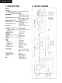
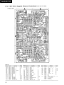
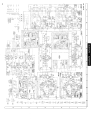
2. BLOCK DIAGRAM
0~
1. SPCIFICA TlaNS
AU-717
;;'1 ~
7'"
Power output
Min. RMS, both channels driven , from 20 to 20 000 Hz , with no
more than 0. 025% total harmonic distortion
85 watts per channel into 8. ohms
Load impedance.
. . . . . . . . 8 ohms
,I~
t --------_
:i!!:i!!, -
20 to 20 000 Hz at or below
Power bandwidth.
rated min. RMS power output
and total harmonic distortion
Total harmonic distortion
,'j + _';;
-
r----____n n_____------
(POWER AMP IN)
less than 0.025% at or below
rated min. RMS power output
Intermodulation distortion
(70 Hz: 7 kHz = 4:1 SMPTE method)
'...........,.... lessthanO. 025%
Frequency response
(at 1watt) (POWER AMP IN)
:r:t:
UUII
, 'I
--' a: I
..................,.. Oto200 OOOHz+OdB-3dB
(PHONO) . . . . +0.2 dB - 2 dB
RIAA curve daviation
(20 to 20
Damping factor.
000 Hz)
approximately 60 at 8 ohms
0.. I
'" I
load
(1 kHz , for rated power output)
PHONO "
" 2. 5mV/47kilohms
(Max. input capability; 350 mV at 1 kHz , less than 0.01 % total
Input sensitivity and impedance
0.. I
Ln_____- _n_______n__-
harmonic distortion)
AUX ,
TAPE. . . . . . . . .
Output level
n__----_n
150mV/47 kilohms
(1 , 000 Hz)
TAPEREC(pinjack) "
150mV/47kilohms
PREOUT
1V/47kilohms
Channel separation
(1 kHz , at rated power output)
PHONO "
betterthan60dB
AUX..................
betterthan65dB
(short-circuit, A-network)
PHONO .......... 78dB
AUX..............
100dB
Hum and noise
Controls
BASS.
Tone selector
TREBLE
Toneselector...........
FILTER.........
HIGHFILTER............
SUBSONIC
MUTING
LOUDNESS (- 30dB) .,.
:!:10dB (50 Hz)
200
400 Hz
ttJ~
:!:10dB (15kHz)
, 6 kHz
3dB(16Hz), 6dB/oct
3dB (10kHz), 6dB/oct
20dB
9dB at 50Hz
7dBat10kHz
"'I
Power requirements
Powervoltage............. 100 , 120 220 240V (50/60Hzl
120V (Usable 110 - 130V)
60 Hz (for U.
A. & Canada
only)
Power consumption
Maximum consumption. .
Rated consumption
Dimentions................
735 watts
425 watts 500 VA
430mm (16- 15/16" ) W
168 mm (6-5/8" ) H
389mm (15- 3/8" ) D
Waight
8kg (39.2lbs) net
":"1
IIA
JlI'-
Ii;;;
0..
II,
JI'"
I:~
I:~
""I
:: I
,21
:51
"(0
L______--
d ..:..
JL______-
19. 8 kg (43. 7 Ibs) packed
r--------- ---------------------
1'-'
"'I
I
~
""
I
~I
"gl
=1
..:..' u
0..
L______- - ------------- -- - -- - -
~r----(0 -(0
-------------
i'i~
L__- -- - --
"C0 -(0"-
- c0~---
&ii&ii
--.,.
... ........
'-'
........
AU- 517/717
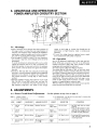
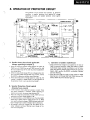
3. ADVANTAGE AND OPERATION OF
POWER AMPLIFIER CIRCUITRY SECTION
DOl
ZDOI
FETOl"
ZDO2
1. Advantage
OThere is neccessity not to decrease the phase response till
DC range in order to increase the music signal response of
extremely low frequency range. Therefore, this amplifier is
employing no capacitors except ones for phase compensation , and has an almost perfect transient characteristics.
0 The first stage FET (2SK9?) is a dual FET of even characteristics and has a large Gm and no- leakage current at normal
temparature.
To avoid the influence by temperature drift , such as center
voltage (OV) deviation , this FET is used as differential amplifier and operates at cross point which is the optimum
point of drain current (at about 3mA) against the temperature drift.
OTransistors , TROS and TRO? , the push- pull pre- driver stage
functions as current differential amplifier that the stabilized
operation can be obtained. In addition , the collector current of these transistors is enough high to make linearity
excellent.
OSince this Amplifier employs phas~ advancer circuits (CO6
COB , C1S , R29 , C16 and R30J, which have not been fre-
quently used
, to compensate the phase characteristics on
high frequency range and is also made to have
enough
current on each stage
to increase the through- rate , the
performance on high
frequency range is conspicuously
improved.
OTo avoid the voltage
deviation ,
regulated power supply
circuit composed of ZDO1 , ZDO2 is employed.
2. Operation
The use of differential amplification at first stage dual FET
(FETO1 , FETO2) and connection of the FET to the differential
amplifier composed of TRO1 , TRO2 , make possible to obtain
enough gain and remarkable low distortion.
The output signals of TRO1 and TRO2 are untiphase.
The output signal of TRO2
adds to TROS , on the other hand
the output phase of TRO1 is inverted by TRO3 ,
then , it becomes
input signal of TRO4 and TRO? which are cascoded connection.
The output signals at TROS and TRO? are inphase that the operation of this stage is push- pull drive and current differential
amplification. The power amplifier of the final stage is composed ofSEPP (Single Ended Push-Pull) symmetry comple
mentary in 3- stage darlington connection type.
TRO9 and TR10 are composing current limiter circuit to protect
power transistor from break- down by overload.
4. ADJUSTMENTS
1. Driver Circuit Board Adjnstments
Note: 1.
(See
the picture of top view on page
Minimum
Master Volume....
3. For adjustment , run the unit for
RoomTemperature................
STEP I
OUTPUT I
SUBJECT I EQUIPMENT
more than 3 minutes after
the power is switched on.
ADJUST
CONDITION
ADJUST FOR
I MEASURE
DCOV
DC Volt Meter
Speaker Terminal
DCOV
F-2721
DC OV:tSmV
Same as above
Same as above
F-2722
0 Then , for the purpose of pro-
DC OV:tSmV
VRO1 , VRO2
Bias Current
Same as above
TP Terminal (+) (-)
F-2721
of F-2721
VRO3
0 Set VRO1 and VRO2 to center
position.
VRO1 , VRO2
L-CH
ceeding the accurate adjustment , set the voltage to 0 volt
by VRO1 first and VRO2 next.
DC 20mV:t1mV
0 By turning VRO3 counterclock-
wise ,
the bias current is de-
creased gradually.
Bias Current
Same as above
TP Terminal (+) (-)
of F-2?~
F-2722
VRO3
DC 20mV:t1mV
AU- 517/717
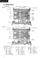
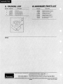
5. OTHER PARTS
1. Top View'
(AU-
517)
Speaker Terminal 8P Input Terminal
4P Input Terminal
Power Cord
Ground Terminal
CO701- CO703
TR703
TR701
C703
T70J
VR02
VR01
VR03
C701
C704
T702
VR01
VR02
VR03
C702
TR702
TR704
R701, R702
Speaker Terminal 8P Input Terminal
(AU- 717)
4P Input Terminal
round Terminal
Power Cord
CO701- CO703
TR703
TR701
C703
T701
C701
C704
T702
C702
TR702
TR704
R701, R702
Parts List ~AU-517/717?
Parts No.
Stock No.
Description
ClO5
C707-714
0659801
0602109
1.0pF 100V M.
R701,7O2
0202221
2200 2W NH.
C0701-7O3 2450060
5066280
2290190
3800010
3800190
3800320
2300060
2300090
2410091
2410830
2411240
2230052
OlpF 150V M.
AC 0,11., XX
AC 0",., EU,
Sp.ok., r.,m;"ol
Pow., Co,d XX
Pow., Co,d EU
Pow., COld 85
Pow., F". Hold.,
Pow., F". Hold., EU. 85
Vollog. S.I.clOt Pl'g XX
Vol log. S.I.ctOl Sock.' XX
AU-517 OnlY
TR701.702 0306450TR703, 704 0300830-2
Parts No. Stock No.
Description
Parts No. Stock No.
Voltage S.I.cto' SW EU. 85
Gm""d r.,ml"ol
2SCI403AR,
2SA745A R, 0, Y
r,o","'o,
C701-704
0559518
12000pF 63V E.
T701.702
4002590
4002594
4002592
Pow., r,o",10,m., XX
F7O1
0432270
0432500
0435140
Pow., r,0",10,m., EU. 85
Pow., r,o",10,m., Ul. CSA
5A 125V
7A 125V ow., ".
5A
Pow., F". EU, 85
Description
AU-717 Only
TRlOI, 7O2 0305840-2
TRlO3,704 0300520-2
2SCI116R,
2SA747 R, 0, Y
r,o",I,'o'
ClOt-704
0559520
15000pF 63V E.
T7OI,7O2
4002580
4002584
4002582
Pow., r,o"do,m., XX
0432290
0434060
0435150
5A 125V
F70t
Pow., r,o",fo,m., EU. 85
Pow., r,o",fo,m., Ul. CSA
lOA 250V Pow., F".
15A Pow., F". EU.
AU- 517/717
(AU- 717)
2. Front View
Parts List ~AU-517/717/
P."s No.
Stock No.
1015170.
15318850
Descdpt;on
(326620
5286721
L=25 P=5
1131400
2430290
5006670
5336600
0319110
5507070
7 Type Koob
1015230.
15318840
100'0 (C)x2 T,eb". 80", Vol,m,
L=25 P=7
7 Type Koob
1101780.
15318840
'Olo,y Switch, Sp,ok",
1190410
15318840
'oto,y Switch. Top' Copy
7 Type Koob
1190410
15318830
'otOty SwiJ,h. 'op" Sel,"ot
1171150
15326611
Le"t Switch
Koob
L"" Switch,Tooe Del,ot
L"" SwitchKoob
1171630
1171120
15326611
11 711 20
15326611
1 090250
15318860
7007580
5058740
La,et Switch. Pow"
L"e' SwiJd.
P.", No. Stock No.
AU- 717 Only
!5326611
P"h Switch Koob
Koob G,ide
P"h Switch.
Top, Ploy
Haod Phooe Jock
8000ot
11 71130
!532661 I
1171130
So",,, 80dge
light Emitt,d Dioda
1090280
15318860
Leg
1171120
15326611
AU-S17 Only
7 Typa Koob
1171610
r326611
De,cdpt;on
Stock No.
P.", No.
7 Type Koob
250kO (MN)x2 80'00" Vo"me
Powat EU. 8S
Le,et Switch Koob
Le,et Switch, Lo,doe,
L"" SwiJd Koob
Le", Switch,
S,b,ooic Filtet
7 Typa Koob
1171130
15326611
5286721
1131400
r326620
7007570
5058730
0319110
150,OX2Vol,meL=25P=7
FtC" Pooel A"y
80ttom Plote
De,c';pt;on
Le"t Switch
Koob
L"" SwiJd. Lo,do"
L"" SwiJ,hKoob
L"" Switch.S,b,oo', Filt"
7 Type Koob
150l0 x2 5kO x 2VoI,me L=25 P=9
Le'et SwiJd Koob
Le", Switch.
M,tiog
Le"t Switd Koob
Le'at SwiJd, High Filtet
P"h Switch Koob
Koob G,ide
P"h SwiJch.
T"o 0",
Fto" Pooal A"y
80ttom Plote
Light Emitt,d Diode
. Figures
Connectors & Pin Ass
Connectors
Type A (3-10 pins)
Pin Ass
Type B (2-6 pins)
Slock No.
Type A (3-10 pins)
TypeB(3-10 pins) Type C (3-10 pins)
2 p,ns 2420450
3 Pins 2420460
3 P'n~ED) 2420650
4 PInS 2420470
5 Pins 2420480
6 PInS 2420490
NOTE: Since stock number of Jamale connectors (type 61 with wires are not
shown in each parts list of Complete crrcUit board , please refer to the
Type D (2-6 pins) Type E (2- 6
above parts list when ordering the connector.
Abbreviations
: Carbon Resistor
: Solid Resistor
Ce.
: Cement
C.
: Bi. Polar
Mi.
: Ceramic Capacitor
: Mica Capacitor
Resistor
: Metal Film
Resistor
: Fusing Resistor
: Non. lnflammable
Resistor
: Mylar Capacitor
: Electrolytic Capacitor
BP.
Electrolytic
Capacitor
: Oil Capacitor
: Polystyrene Capacitor
: Tantalum Capacitor
pins)
) ~
AU-517/717
6. PARTS LOCATION & PARTS LIST
Since some of capacitors and resistors are
omitted from parts lists in this Service
Manual , refer to the common parts list for
capacitors & resistors which was appended
(AU-517 Stock No. 7595201)
(AU-717 Stock No. 7595171)
Terminal Circuit Board
Conductor Side
previously to each Sansui Manual.
Parts List
Parts No. Stock No.
2200480
2 F-2723
ualizer
Description
8P lop"' Te.miool
(AU-517 Stock No. 7551171)
(AU-717 Stock No. 7551161)
Circuit Board
Conductor Side
Parts List
Parts No.
TRo"o,
TROO.
TR05.
TROl.
TRoo.
TRll.
De.cr'ption
Stock No.
2SA906 (G. H)
0300470. 1 2SA726(w) (F. G)
0300900. 1 2SA906 (G. H)
0306290. 1 2SC140011) (E.
0300B90.
2SA750(3) (E. U)
0306290.
2SC14001I) (E.
0300900.
TRI3.
TR15
0306290.
DOI.
Doo. 04
0340120
0340120
2SCI4001I)IE.
0300890. 1 2SA750(3) (E. U)
T.oo,'sto.
Position
, B. 2 B
1 A. 2 B
1 B. 2 B
1 B. 2 B
1 A. 2A
1 A. 2A
1 A. 2A
1 A. 2A
VO1212 )
1 A. 2 B
VO1212 Vo"sto.
1 A. 2A
Ports No.
Description
Stock No.
COI.
COl. 08
CI3.
C15.
C23.
0602109
0620121
0620151
0625272
0625103
RI7.
RI9. 20
R23.
R33.
R35.
0231561
0231220
0231273
0231153
0231304
1.0pF 100V
120PF
150pF 50V
2700pF
10000pF
'"0
nrJ
27krJ
15krJ
300krJ
y,W
Position
1 C.
18. 2 B
1 A'
1 A. 2A
1 A. 2A
1 A. 2A
1 A. 2A
1 A. 2A
1 A. 2A
1 A.
Ports No.
Description
Stock No.
R47.
R49.
0193820
0193820
SOl
502
1190420
1190410
2410920
82rJ
82rJ ,W
lop", Ro'o.y Switch
Tope Copy Ro'o.y Switch
3P Pio A,, y Type E
AU-7T7 Only
2410910
2PP'"A,, yTypeE
Position
1 A. 2A
1 A. 2A
1 B. C
2 B. C
AU- 517/717
3. F- 2673
Tone Control Circuit Board
(AU-517 Stock No. 7561841)
Conductor Side
Parts List
Pa.ts No.
Stock No.
TRol.02
TRO3.
TR05.
TRoUB
4. F-2674
Bass & Treble Volume Circuit Board
Dese.'ption
E)
0306010.
2SCI222!2) (U. E) f
2SCI222!2)(U.
0300890. I
2SA750(31 (E. U)
0306010.
2SCI222(2) (U. E)
Dol. 02
0340120
VD1212
COl.02
C05.
0610361
060233B
VROI
1015170. I
SOl
S02
SO3
1171120
1171150
1171120
2410570
2410920
0306010. I
posmon
T,o""!o,
Vo';"o,
lB. I A
lB. I A
1 B. I A
1 B. 2 B
360pF 50V
33pF 100V
250kO(MN)x2 BoloooeVR2A
lood"" lem SwHoh
Toos Deleo! lew SwH,h
Sob'o,l, Fllte' l.,a, SwH,h
5P PI, A,, y Typa D
2A. B
2B
2B
3PPI,A,, yTypaE
(AU-517 Stock No. 7561861)
Parts List
Pa.ts No. Stock No.
VROI.02 1015230.1
5. F- 2670
Pre-
Main Switch Circuit Board
Dese"ption
IOOkO(C)x2 T,abla. Bo"
(AU-517 Stock No. 7595211)
(AU-717 Stock No. 7595191)
Parts List
Parts No. Stock No.
SOl
6. F- 2667 Ta
e Pla
Circuit Board
1110290
2200500
Dese"ption
PRE-MAIN Sllda Sw'Ioh
4P I,po' !a,m',ol
(AU-517 Stock No. 7595181)
(AU-717 Stock No. 7595221)
Parts List
Pa.ts No. Stock No.
SOl
1131400
2410700
2410920
Dese"ption
Topa P"h SwHoh
6P PI, A,, y Typa F
3P PI, A,, y Typa E
Voloma
AU- 517/717
7. F- 2720
(AU-717 Stock No. 7561941)
Tone Control Circuit Board
Conductor Side
, Parts List
Pacts No.
TRO1,
TR03,
TRos, 06
TR07,
TR09,
TRII,
TR13, 14
Desc'iption
Stock No.
0360370-2
0300470,
0306290,
0300890,
2SA798 (F, G, H)
2SA726M') (F, G)
2SCI400(1) (E, U)
2SA750(3) (E. U)
2SCI400(I) (E, U)
030629D,
03D6290, 1 2SCI4DO(1) (E, U)
0300890, I 2SA750(3) (E. U)
8. F- 2665
Position
lB. 1 A
1 C. 1 A
I C. l A
T,o","'o,
1 C. 1 A
1 C. 1 A
1 C. 1 A
1 C. 1 A
Pacts No.
DO1,
Cor. 02
COS,
C09,
R37,
R39,
VRO1
Desc,iption
Stock No.
0340120
0620361
0602338
0620121
Dl91820
0191820
1015170.
VD1212 Vo""o'
360pF 50V
33pF 100WV
120pF 50V
820
Position
1 C. 1 A
2B
lB. 1 A
1 C. 1 B
1 C. l A
\!4W
820; 4
Pa"s No. Stock No.
SOl
S02
S03
S04
505
250kO(MN) X 2 8010ooe VR
1171130
1171130
1171150
1171130
1171130
2410570
2410920
VROr.02 1015230,1
Conductor Side
lo,doe" SW
2B
Tooe Deleot SW
S,b,oolk FII", SW
High Fllte, SW
2B
5P Plo A" y Type D
3P Plo A"y Type E
Parts List
Pa,ts No. Stock No.
Turn Over
Position
(AU-717 Stock No. 7561851)
Bass & Treble Volume Circuit Board
Conductor Side
9. F- 2666
Desc,iption
MO1log SW
Switch Circuit
Board
Desc,iption
100kO(C)X2 T,eble, Bo"Vol,me
(AU-717 Stock No. 7561871)
Parts List
Pa,ts No. Stock No.
SO1
1131410
Desc,;ption
T010 am
P"h
"""'
~~g
AU- 517/717
10.
(AU-517 Stock No. 7571721)
(AU-717 Stock No. 7571741)
21 Driver Circuit Board
Conductor Side
Parts List
Pa,ts No. Stock No.
TRol
TR02
TRo3
TR04
TRo5
TR06
TRo7
TRoa
TRoo
TRIl
TR12
TR13
0306290. 1 25CI400111(E. U)
0306290. 1 25C140011l(E. U)
25A750(3) (E. U)
0300690.
0300890. 1 25A750(3) (E. u)
25A899 (6. V)
0300791.
0305951. 2 25C945 (G. p)
0306401. 2 25C1904 (6. V)
0306401. 2 25C1904 (6. V)
0305951. 2 25C945 (G. P)
0300791. 2 25A699 (6. V)
25D362 (M. l. K)
03084410303271. 2 256537 (M. l. K)
fTor
0370251. 2
Dol
D02
Do3
0311160
0311160
0311160
Do.
11. F- 2722
Driver Circuit Board
Conductor Side
R-ch
(AU-517 Stock No. 7571731)
(AU-717 Stock No. 7571751)
Dasc"ptlon
0311160
10311160
25K97
Posmon
1 A. 3 D
1 A. 3 D
1 A. 3 D
1 A. 3 D
1 A. 3 D
T'o,,;$lo'
16.
1 A. 3 D
26.
1.26. 3.4C
16.
26.
1 B. 3C
fET
1 A. 3D
1 52473D
152473D mode
152473D
151566
2A.
EG6O1E 601.
2A. 4 D
1 A, 3D
1 B. 3C
2 B. 4C
ZDol
ZD02
0316170
0316170
Cor
CO5
CO7
0620101
0620331
Ro.
Ros
Ro,
Roo
RJO
R28
R3I
R36
R37
R43
R44
R45
R46
R.7
0202222
0231332
0231332
0103392
0202152
0210470
0210470
0103560
0103560
0103479
0103479
0135338
0135338
0202100
0132229
lor
4210290
I.5pH Co;!
2A. 4 D
VROI
VR02
VRO3
1033570
1035330
1035310
1000(6) Vol,ma
2'0(6) Vol,ma
!k0(6) Vol,ma
2A.
0669505
laM' D;oda
100pf\
330pfl 50V P.
5pf 50V C.
2'0 2 W N. J.'.
3'0\ "
3'01 "W M.
9kO
YzW
1.5'0 2W N.J.
470\ "
4701 "W N. J.'.
2A.
2A.
1 B. 3C
2A. 4 D
2A. 4 D
2A. 4 D
1 A. 3D
1 A. 3D
2A.
1 A. 3D
26.
70 "W
"
CR.
330\
3301 5 ~ Ca.
100 2W N.J.
20 2 W Ca.
1 B. 3C
2 B. 4 D
1 B. 3C
2 B. 4C
2 B. 4C
2A. 4c.D
2A.
1 A. 3D
1 A. 3D
AU-517 Only
R03 0107102
R16 0107223
R28 0210560
R31 0210560
"0\
22'01 "
W.
560\ "
5601 "W N. J.'.
1 A. 3D
lA. 3C.
2A.
1 A.
AU-717 Only
RO3 0107122
R16 0107273
R22 0107103
R28 0210470
R31 0210470
1.2'O
2nO y.,W
10'0
470
CR.
470 .2W N. J.'.
1 A.
1 A.B. 3C.
1 A.
2A. 4 D
1 A. 3D
Ltlr G-e
(j I
AU- 517/717
12.
(AU-517 Stock No. 7502331)
2675 Power Supply & Protector Circuit Board
Conductor Side
Parts List
P.,ts No.
D.se"ptlon
Stock No.
TRoL02
TR03,
TR6or
TR602
TR603
TR604
TR605
TR606
TR607
2.5D438 (E, F)
25B560 (E, F)
0305951, 2 25C945 (Q. P)
0305951, 2 25C945 (Q, P)
0305951, 2 25C945 (Q, P)
0300.510,
25A733 (P, Q)
0305951, 2 25C945 (Q, p)
0305951, 2 25C945 (Q, P)
0305951, 2 25C945 (Q, P)
DOL 02
D03,
Des. 06
D07.
D09,
0311530
0311530
0311530
DII,
DI3,
D15,
0311.530
0310350
03103.50
03103.50
0310350
T,a"I"ar
2B
2B
2B
2B
I A. 3A
30D2
30D2
30D2
30D2
10D2(152227)
1 OD2 (152227)
1 OD2 (152227)
1 OD2 (152227)
Position
1 B. 3 B
1 B. 3 B
2B
2B
0308.521, 2
0303361, 2
1 A. 3 A
1 A. 3A
Dlod.
1 B. 3 B
1 B. 3 B
1 B. 3 B
3 B. 3 B
P.,ts No. Stock No.
D17-18
DINO
D6or
D602
D603
D604
D605
D606
D607
D6O8
(0311160
0311180
(0311160
0311180
0310350
0310350
0311160
0340120
0311160
0311160
0311160
0310340
D.se"ptlon
152473D
151588
152473D
151588
10D2 (152227)
Position
2B
2B
10D2(152227)
152473D
VD1212 Vari"or
152473D
Dlod.
2A
2A
2B
2B
2B
2B
2B
C603
ROL 02
R03.
Res, 06
R07,
RI9.
R6or
R602
R6I6
Rl601
10Dl (152226)
RD33E (B) r
ZDor,
ZD03.
ZD601
ZD602
0316570
0316570
0315760
0316390
RD33E (B)
Z, r DI
EQAOI. 06R .. 0
RD6.2E (B)
COI-02
0655103
10000pF
500V
1 B. 3 B
1 B. 3 B
2B
2B
1 B. 3 B
D.se"ptlon
Pa"s No. Stock No.
FOL 02
0602338
33pF
0202272
0202272
7kO
7kO
0210101
0210101
0202100
0202391
0202222
1000
0210472
r1150370
150250
0435160
0432300
0435160
2310220
2310230
1000t r;,W
2
100
3900 2 W
J.R.
1 A. 3A
1 A. 3A
J.R.
2 B. 3 B
1 B. 3 B
J.R.
2kO
7k0
y,W
Position
2B
100WV
J.R
2B
2B
2B
R.lay
R.lay
4A 12.5V Pow., I". Ul, C5A
6A 125V AC f". XX
4AAC I". EU.
F". Hold.r
F". Hold.,EU. B5
1 B. 3 B
AU- 517/717
13. F- 2663
(AU-717 Stock No. 7502321)
Power Supply & Protector Circuit Board
Conductor Side
Parts List
Parts No.
TROJ.
TRo3.
TRo'.
TRo7.
TR09.
TR11,
TR601
TR602
TR603
TR60.
TR60'
TR6"
TR607
Dol,
Do3.
Do"06
DOl. os
Do,. 10
DI!.12
Description
Stock No.
18. 3 B
2B
1 B. 3 B
250356 (0. E)
25B526 (0. E)
0306270. 1 25C1708 (E, U)
030071 O. I 25A847(I)(f. G)
0306270. I 25CI708(f.
0308451.
0303281. 2
0300710,
2SA847 (f, G)
0305951. 2 25C945 (Q, p)
0305951. 2 25C945 (Q. P)
25C945 (Q. P)
0305951,
25A733 (P.
0300510,
0305951. 2 25C945 (Q. P)
25C945 (Q. p)
0305951.
0305951. 2 25C945 (Q, P)
0311290
0311300
0310350
0310350
0310350
0310350
55.
55-
Position
T,oO$lst..
1 B. 3 B
2B
2B
IB
1B
1 A.
1 A.
1 A.
1002(152227)
1002(152227)
1002(152227)
I A.
I A.
1002 (IS2227)
1 A. 3A
P.rts No.
D13-14
DI5-16
D"-18
D6o'
D6o2
D.o3
D6o4
D6os
D606
D607
D6o'
D609
D6IO
ZDo!.02
ZD601
ZD60'
Description
Stock No.
(0311160
0311180
0311180
10311160
0311180
10311160
0310350
0310350
0311160
0340120
0311160
, 0311160
0311160
0310340
0340120
0340120
0316310
0315760
0316390
1524730
Diode
151588
1524730
151588
1524730
151588
Po.ltlon
1 B. 1 A
lB. 1
1 B. 3 B
1002(152227)
1002(152227)
1524730
VO1212 Vodsto,
1524730
1524730
DIode
1524730
P.rt. No.
CO!.02
CO3.
C603
0655103
0655103
0602338
RO!.O2
RO3.
0202332
0202332
Ro""
2B
2B
2B
2B
2B
RI5,
R37,
R60'
R602
R603
R6"
1001 (152226)
VO1212
RL601
VO1212 Vo",'o'
Fo!.02
F01-0'
RO-13E (B)
EQAOI. 06R
RO. 2E (B)
1 B. 3 B
Z.n., Diode
1A
D..crlptlon
Stock No.
0210101
0210101
0202100
0202391
0202272
0202272
0210472
("50250
1 A.
1 A.
2B
1O000Pf
10000pf 1 500V
33pf
100WV
3k0
3kO 1
2W
Po.ltlon
N.I.
1000
10001 y,w
2
1 A.
1 A.
1 B. 3 B
2B
lOO
3900
7kO 2 W
7kO
7kO
y,W
I.R.
2B
2B
2B
I.R.
1150370
R.loy
R.loy
0432290
0432500
0435170
2310220
2310230
5A 125V Pow., fuse UL, C5A
7A 125V AC Ius. XX
5A.
AC luso EU, B5
fuse Hold., XX
fuse Holde, EU, B5
I A.
1 A.
AU- 517/717
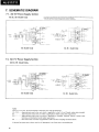
SCHEMATIC DIAGRAM
7.
7-1. AU-517 Power Supply Section
xx EU. BS Model Only
: La D'esent;an et res sDec;ficat;ans sant suscept;b'es d'
e mad;fiees sans p'eav;s Da' su;tes d' amel;a,at;ans eventuelles.
And",ungen , d'e dem technoschen Fa'tsch"" d,enen. ble'ben va'behalten
. Des;gn and spec;ficat;ans subject to change w;thaut nabce fa' ;mp'avement.
AC ;~~:;;g
r"_,, 4'T
50/60H,
s""
xx Model Only
EU. BS
Model Only
7-2. AU-717 Power Supply Section
xx EU. BS Model Only
PC",
rWHtTE-
F",
F",
'OA I-OO-;'OV
5A-220-240V
JSA-T
is",.
FOJ
AC
FOT-Q4
7A 72SV
50/60Hz
xx Model Only
AC 220,240f'
50H,
F,,_~ 5A-T
EU. BS
Model Only
NOTE:
AS to U. , c.S.
, B.5., ES and XX marked in the Parts Lists , note the followings:
, c.S. A... . Approved parts used in the unit which is applicable to the U.5. and Canada under safety standard.
S. ......... . Approved parts used in the unit which is applicable to British under safety reguirement.
U. .. . . . . . . . . Approved parts used in the unit which is applicable to Sweeden , Denmark , Norway, Finland , West
Germany, and Switzerland under safety reguirement.
XX ..........
Parts used in the unit
which is applicable to other countries excepting mentioned above.
* In parts lists , parts with no above mark in of " Description " are all the same as XX marked parts.
5-",
Po...r
S""b
5"".-
F-2870
PRE P- OWER
So,"",
S".-
S"'.
SOT"~
S"',
S".-
s".-
Speak""
F-2673
2673
Loudn"s
F-2673
2667
Tope pz"y
Subsonic Filter
2?23
Tape Copy
Tone
2n3
61 iJ:\:6
S"ector
PHONO
PHONO
RIGHT CANNEL
rREC
TAPELPLAY
r-- 2
6691
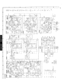
7-3. AU-517
1. off
2.
3. 8
4. A+B
1. off
2.
g:;':;~o ":::::CED
.,f",
2.
1. off
2.
1.
2.
1. off
2. 16Hz
1. CONNECTED
'.pd
1. 5""""
"pe-7
1. source
50201
50"2
2. off
3. source
tuner
1. phonO-2
1. hono3. wn"
4. au'
;:,.
SEPARATED
*1. METAL FILMRESISTOR
TOLERANCE
*2. NON FLAMABLERESISTOR
*3. FUSING
RESiSTOR
ALL RES'STORS
!Ii WATTS
UNLESS OTHERW'SE
NOTED
SYM80L
CERAM'C
MYLAR
STYROL
JAPANMod,IO'IJ
AC ,ooV
SO/50Hz
C", 0.
S",
i:J
RED
BROWN
RED
PT",
PURPLE 104
3s.
:::1'
eRAY
PURPLE
3s.
Ii"
69,J
087"
PURPLE
35.5V 05
eRAY
-----
TR"
2SD438(E,
I'?
J,:
~=--AU- 517/717 AU- 517/717
---
UI 2SA750IE,U)
01!
2SCI2221E,
BROWN PT", PURPLE
3S.5V
L__-
2~mI F-
~==--.--
-::,
6751
F-ir"ill" -
2SK97
FET"
2?21
;;-j
-;-- '"
c!i
~2K
R,,22K
Sysum A
5",.
2SC9451P,
2SCI9041B,
0 10 1010
TR" 08
TR03.
04 2SA750IE,
TR05. 2SA8991B,
c!i'"
TROo.
CO
TR" 02 2SCI400lE,
+'---"
- -'---"
+
J",
IO(2)
C"
R", 220(2)
c,,
2SD382IK,
TR" 2SB537IK,
TR"
LED",
3002
I =
1l3E
i62E
lAD 1
1801
1824730
VO1212
1001
1002
28K97
28A899
28C1904
B r
258537
280382
28A726
28A847
2SA906
28C1708
FeB
280438
28A733
28A750
230060
28C945
25C1222
25C1400
7-4. AU-717
146
LED",
'"
~Cf400 lE.
H67D
SO"
olf
A'S
F~720'
AC7aoVSa/SOH,
JAPAN
MODEL
ONLY)
ACI1DVSOH,
(UL CSANDOELDNLY)
CONNECTED
g%U
g~~~gjT ;iu;,pE,jJ SEPARATED
off
2~i7S0IE. V)23
s"o.
5"'0"
5",
WATTS
ALL RESISTDRS
NOTED.
DTHERWISE
UNLESS
RESISTOR
METALFILM
TOLERANCE!/%
RESISTOR
*2. NON FLAMABLE
'3. FUSINGRESISTOR
Powa
S"ako"
PRE-POWER
LEDT" LED", LED",
G) "
illfI ~!::'!3 I
112iA906IF,
TR",
SOk.'
dd"t
I.ofl
2.
I.,yff
2.
I.
2.
2SA726 IF,
I ~Dr212
F-1723
LEFTCMANNEL
TUNER
AUX
Sd"tor
5",.
SOle,
507'
2723
2667
Top, Copy
70" Play
5020,
5",,
5",.
2664
F-2664
504",
Moting
L"d""
2664
5"",
F-2664
Sobsoni, Filtor
2664
70n2
High Filta
OnLy)
5"'
C", am
PT,O7
'!l
TR"."
2SCI400IE,
TR"""'3
,,
2SA750IE,
AU- 517/717 ! AU- 517/717
BROWN
REO
2SA899IB.
2SC9451P,Q)
~ ~
--TR"
TR"
TR""
TR"
.l.
2SCI904IB
2SC94~
R,d7We)
RD6.
Z0602
f---"""J3
C"OO47 R" lo(2I
R" '-2
5S3
5S3R
2SA733
2SA750
2SC945
2SC1222
2SC1400
FCB
2SA726
2SA847
2SA906
2SC1708
258526
250356
258537
250382
B r
c:,u:
2SA747
25Cl16
25A899
2SC1904
u I
fCf
2SK97
1001
1002
VO1212
1524730
EQAO1.06R
EQBO122
R06.2E
ROl3E
11 'f1
vrru If~
'"
~~
,": '"'"
"AU- 517/717
8.
OPERATION OF PROTECTOR CIRCUIT
This protector circuit contains two functions at abnormal
condition; a speaker protector circuit against DC voltage
appearing at output , and speaker protector circuit against
over- current.
POWE R OUTPUT
e ?:'
R40
r620
CID
t 1'6.
0602
4'/A
R06.
27K
lR6Ob
CID
'-O
f?5 ',i
8;
'-c'
(3) c::i :~
Ii: ';';5
, ) 0-
0:::
'-?B
r:s
D05,
:jj +1 ~ ,
c,
06. 13.
D603. 605, 606, 1i07
1524730
11;:"' ~.
cfi
LE0701
(5):h
OJ
a., n
~ V,
~~~2 X2 ~
0:::
a:::
(Ji4
ell
i;;
0:::
-d
~ I SS
VOl212
EQAOI 06R
0.04
34137
ZD601
A. Speaker Protection Circuit against DC
voltage appearing at output
1. When an abnormal negative voltage appears at output
TR601 turns off , TR602 turns on and TR603 turns off so that
the relay, RL601 , keeps off in order to protect loudspeakers
1. When control.(bias) voltage is not supplied to the base of
TR607 in abnormal condition , TR606 and TR607 ,
on astable
multivibrator repeat turning (switching) on and off alter-
nately each other by charging and discharging of capacitors
C606 & C607 ,
from break- down.
zero voltage(center voltage) controlling TR607 through D607 will increase , resultly
the LED701 as protector indicator , starts flickering.
3. When abnormal positive voltage appears at output ~, the
voltage is supplied to TR602 directly, and the operation of
the protector circuit is same as above mentioned 1,
2. While the relay, RL601 ,
C. Operation of astable multivibrator
keeps OFF ,
B. Speaker Protection Circuit against
abnormal over- current
1. At the moment when abnormal excessive current flows
into power transistors , a transistor (TR09) detecting excessive over- current , on power stage becomes ON.
2. Then , DC voltage at ~ decreases , resulfly TR604 turns on
and positive certain voltage appears at ~'
3. As mentioned above , when TR602 turns on , the relay, RL601
keeps OFF; a certain positive voltage at~' turns on TR60S
too , resultly collector voltage of TR60S decreases and its collector voltage keeps a certain voltage at ~ simultaneously.
4. By keeping a certain DC voltage at ~. , the LED701 as pro.
tector indicator continues flikering, even though all circuits work completely.
resultly, the LED701 as protector indicator
continues flikering.
2, When the relay, RL601 is turned on , base voltage of TR607
becomes zero volt through D607 and TR606 becomes ON
resultly LED701 as power indicator lights up.