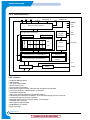
1
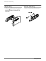
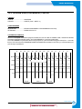
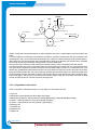
DIGITAL LASER MFP
SCX-5312F
SCX-5112
SERVICE
MANUAL
CONTENTS
DIGITAL LASER MFP
1. Precautions
2. Specifications
3. Disassembly
4. Troubleshooting
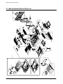
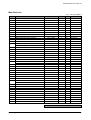
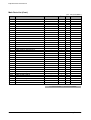
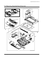
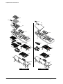
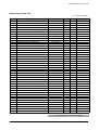
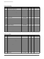
5. Exploded Views and Parts List
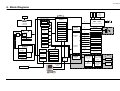
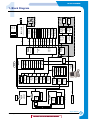
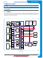
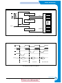
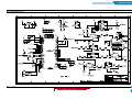
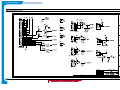
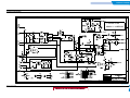
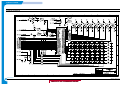
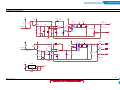
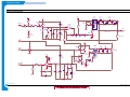
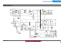
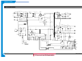
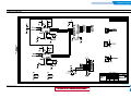
6. Block Diagram
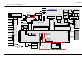
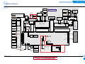
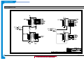
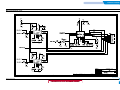
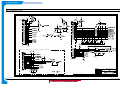
7. Connection Diagram
ELECTRONICS
This service manual is also provided on the web,
the ITSELF system Samsung Electronics Co., Ltd.
“http://itself.sec.samsung.co.kr”
© Samsung Electronics Co.,Ltd. MAY 2002
Printed in Korea.
VERSION NO. : 1.02
CODE : JC-0061A
- This Service Manual is a property of Samsung Electronics Co.,Ltd.
Any unauthorized use of Manual can be punished under applicable
International and/or domestic law. -
This manual is stated and
provided for service description.
All rights reserved. Any parts of the
information in this manual are prohibited
from free duplication, use or translation
without prior written approval except in
cases allowed by the Copyright Act.
Specifications are subject to change without
prior notice.
Samsung Electronics Digital Printing CS Group
Copyright (c) 2002. 5.
Precautions
1. Precautions
Follow these safety, ESD, and servicing precautions to prevent personal injury and equipment damage.
1-1 Safety Precautions
1. Be sure that all built-in protective devices are in
place. Restore any missing protective shields.
2. Make sure there are no cabinet openings
through which people-particularly children- might
insert fingers or objects and contact dangerous
voltages.
3. When re-installing chassis and assemblies, be
sure to restore all protective devices, including
control knobs and compartment covers.
4. Design Alteration Warning:Never alter or add to
the mechanical or electrical design of this equipment, such as auxiliary connectors, etc. Such
alterations and modifications will void the manufacturer’s warranty.
5. Components, parts, and wiring that appear to
have overheated or are otherwise damaged
should be replaced with parts which meet the
original specifications. Always determine the
cause of damage or overheating, and correct any
potential hazards.
6. Observe the original lead dress, especially near
sharp edges, AC, and high voltage power supplies. Always inspect for pinched, out-of-place,
or frayed wiring. Do not change the spacing
between components and the printed circuit
board.
7. Product Safety Notice:Some electrical and
mechanical parts have special safety-related
characteristics which might not be obvious from
visual inspection. These safety features and the
protection they provide could be lost if a replacement component differs from the original. This
holds true, even though the replacement may be
rated for higher voltage, wattage, etc.
8. Components critical for safety are indicated in
the parts list with symbols .
Use only replacement components that have the
same ratings, especially for flame resistance and
dielectric specifications. A replacement part that
does not have the same safety characteristics as
the original may create shock, fire, or other
safety hazards.
1-2 Precautions on Disassembly and Reassembly
Very careful precautions should be taken when
replacing parts. Before replacing, please check
cables because you cannot put the cables that you
removed for replacing parts into the proper place if
you would not make sure of where they were connected and in which condition.
Please do the following before disassembling for a
repair or replacement of parts.
1. Pull out paper cassette, printer cartridge
installed. Especially careful not to be scratched
by the surface of developer or not to expose
them to light.
2. Turn the power switch off.
3. Take out the power plug, printer cable from the
printer.
4. Use only the same type of part as original when
replacing parts.
Samsung Electronics
5. Do not force to open or fasten plastic material
components.
6. Be careful that small parts such as screws
should not get in the printer.
7. When disassembling, assembling, also observe
small components are located in place.
8. If you uncover and turn the machine over to
replace some parts, toner or paper particles may
contaminate the LSU window. Protect the LSU
window with clean paper.
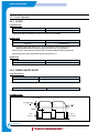
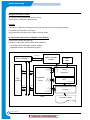
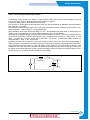
Releasing Plastic Latches
Many of parts are held in
place with plastic latches.
The latches break easily :
release them carefully.
To remove such parts,
press the hook end of the
latch away from the part to
which it is latched.
1-1
Precautions
1-3 ESD Precautions
1. Certain semiconductor devices can be easily
damaged by static electricity. Such components
are commonly called “Electrostatically Sensitive
(ES) Devices”, or ESDs. Examples of typical
ESDs are: integrated circuits, some field effect
transistors, and semiconductor “chip” components.
4. Use only a grounded tip soldering iron to solder
or desolder ESDs.
Use only an “anti-static” solder removal device.
Some solder removal devices not classified as
“anti-static” can generate electrical charges sufficient to damage ESDs.
5.
The techniques outlined below should be followed to help reduce the incidence of component
damage caused by static electricity.
CAUTION : Be sure no power is applied to the chassis
or circuit, and observe all other safety precautions.
2. Immediately before handling a semiconductor
component or semiconductor-equipped assembly, drain off any electrostatic charge on your
body by touching a known earth ground. Alternatively, employ a commercially available wrist
strap device, which should be removed for your
personal safety reasons prior to applying power
to the unit under test.
6. Do not remove a replacement ESD from its protective packaging until immediately before installing it. Most replacement ESDs are packaged
with all leads shorted together by conductive
foam, aluminum foil, or a comparable conductive
material.
7. Immediately before removing the protective
shorting material from the leads of a replacement ESD, touch the protective material to the
chassis or circuit assembly into which the device
will be installed.
8.
3. After removing an electrical assembly equipped
with ESDs, place the assembly on a conductive
surface, such as aluminum or copper foil, or conductive foam, to prevent electrostatic charge
buildup in the vicinity of the assembly.
Do not use Freon-propelled chemicals. When
sprayed, these can generate electrical charges
sufficient to damage ESDs.
Maintain continuous electrical contact between
the ESD and the assembly into which it will be
installed, until completely plugged or soldered
into the circuit.
9. Minimize bodily motions when handling unpackaged replacement ESDs. Normal motions, such
as the brushing together of clothing fabric and
lifting one’s foot from a carpeted floor, can generate static electricity sufficient to damage an ESD.
1-4 Super Capacitor or Lithium Battery Precautions
1. Exercise caution when replacing a super capacitor or Lithium battery. There could be a danger of
explosion and subsequent operator injury and/or
equipment damage if incorrectly installed.
3. Super capacitor or Lithium batteries contain toxic
substances and should not be opened, crushed,
or burned for disposal.
2. Be sure to replace the battery with the same or
equivalent type recommended by the manufacturer.
4. Dispose of used batteries according to the manufacture’s instructions.
1-2
Samsung Electronics
Precautions
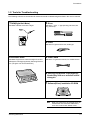
1-5 Tools for Troubleshooting
The following tools are recommended for safe and smooth troubleshooting described in this service manual.
1 DVM(Digital Volt Meter)
3 Driver
Standard: Indicates more than 3 digits.
Standard: "-" type, "+" type (M3 long, M3 short, M2
long, M2 short).
4 Pinset
Standard: For general home use, small type.
2 Electronic Scale
5 Cotton Swab
Standard: Equipment to check the weight of consumables(toner cartridge) supplied by Samsung Electronics. (The gram unit can be measured.)
Standard: For general home use, for medical service.
6 Cleaning Equipments a IPA(Isopropyl
Alcohol)dry cloth or a soft stuff neutral
detergent.
7 Software(Driver) installation CD ROM
Note : Mind your hands not to be touched when you
disassemble and reassemble PBA ASS'Y,
such as the main board, SMPS, HVPS.
Samsung Electronics
1-3
Specification
2. Specification
Specifications are correct at the time of printing. Product specifications are subject to change without notice.
See below for product specifications.
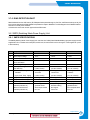
2-1 General Specifications
Item
Description
Type of Unit
Desktop
Operation System
Win95/98/ME/ NT /2000/XP
Duplex Printing
Yes(Default)
Interface
IEEE1284(Nibbel/ECP)
USB(without HUB mode)
CPU
66 MHz(KS32C61200)
Emulation
PCL6
Warming up Time
41 Sec (Stand-By), 25˚C
Absolute Storage Condition
Temperature : -20°C ~ 40°C,
Humidity : 10% RH ~ 95% RH
Operating Condition
Temperature : 10˚C ~ 32˚C,
Humidity : 20% RH ~ 80 % RH
Recommended Operating Condition
Temperature : 16°C ~ 30°C,
Humidity : 30% RH ~ 70% RH
Dimension(W X D X H)
560 X 433 X 459 mm
Weight
About 22.5 Kg(with CRU)
Acoustic Noise
Less than 56/47 dB(Copy/Printing mode)
Power Rating
AC 100VAC ~ 127VAC ± 15 %, 50/60Hz ± 3Hz
AC 220VAC ~ 240VAC ± 15 % , 50/60Hz ± 3Hz
Power Consumption
Avg. 320Wh ( No load Condition)
Power Save Consumption
Avg. 35Wh
Recommended System Requirement
Pentium II 233 Mhz, 64 MB RAM, 120MB(Hard Disk)
Minimum System Requirement
Pentium II 400Mhz, 128 MB RAM, 220MB(Hard Disk)
LCD
16 characters X 2 lines
Memory
4 Mbyte for flash Memory , 16 Mbyte for DRAM
Samsung Electronics
2-1
Specification
2-2 Printer Specifications
Item
Description
Printing Method
Laser Scanning Unit + Electro Photography
Speed
Single Side : 12 PPM
(Letter Size, 5% Character Pattern)
Duplex : 7.5 IPM(Images/Min) (Letter Size, 5% Character Pattern)
Source of Light
LSU(Laser Scanning Unit)
Duplex Printing
Yes(Default)
Resolution(Horizontal X Vertical)
True 600 X600 DPI , 1200 DPI Class
Feed Method
Cassette Type , By Pass Tray,
ADF(Automatic Document Feeder)
Feed Direction
FISO(Front-In Side-Out)
Paper Capacity(Input)
Cassette : 550 Sheets
By Pass Tray : 100 Sheets(based on 75g/ß≥, 20lb)
Paper Capacity(Output)
Face Down : 250 Sheets
Effective Print Width
203 ± 1mm (8 inch)
2-3 Facsimile Specification(SCX-5312F Only)
Item
Description
Standard Recommendation
ITU-T Group3(ITU : International Telecommunications Union)
Application Circuit
PSTN or behind PABX
(PSTN : Public Switched Telephone Network.
PABX : Private Automatic Branch Exchange)
Data coding(Compression)
MH/MR/MMR/JPEG(Transmission)
Modem speed
33600 /14400/12000/9600/7200/4800/2400 bps
Transmission Speed
Approximately 3 sec(33,600 bps)
Effective Scanning Width
8.2 inches(208 mm)
Halftone
256 Levels
Paper Capacity(Input)
ADF(Automatic Document Feeder) : 30Sheets(75g/ß≥)
FAX Mode
Standard /Fine/Super Fine/Halftone
Memory
4MB
2-2
Samsung Electronics
Specification
2-4 Scanner Specification
Item
Description
Type
Flatbed(with ADF)
Speed
Mono : 1.25 msec/line, Color : 5 msec/line
Device
Color CCD(Charge Coupled Device) Module
Interface
IEEE1284(ECP Support)
USB(without HUB Mode)
Compatibility
TWAIN Standard , WIA
Optical Resolution(H X V)
600 X 600 dpi
Interpolation Resolution
Max. 4800 dpi
Halftone
256 Levels
Effective Scan width
8.2 inches(208 mm)
2-5 Copy Specification
Item
Description
Mode
B/W
Quality
Text/Photo/Mixed
Mono Copy Speed(1)
Platen(SDMP) : 12 cpm
ADF (SDMP) : 12 cpm
ADF (MDSP) : Text/mixed : Approx. 7 cpm
: Photo
: Approx. 3 cpm
Optical Resolution (H x V)
600 X 600 dpi
Multi Copy
99 pages
Maximum Original Size
Legal
Maximum Page Size
Legal
Paper Type Selection
Plain , Legal , Cardstock , Transparency
Zoom Range
Platen : 25 ~ 400%(1% Step)
ADF : 25~100 %(1% Step)
NOTE :
(1) Speed claims based on the test chart : Letter size.
SDMP : Single Document Multiple Printout
MDSP : Multiple Document Single Printout
Samsung Electronics
2-3
Specification
2-6 Telephone Specification(SCX-5312F Only)
Item
Description
1Touch Dial
40EA(1~20 , shift key + 21~40)
Speed Dial
80EA
Tone/Pulse
Tone only user modeTone/Pulse selectable in tech mode.
2-7 Consumables
Item
Type
Life
2-4
Description
Separate type
(Toner Cartridge / Drum Cartridge)
Toner Cartridge
6,000 sheets
( 5% coverage pattern, simplex normal mode )
Drum Cartridge
15,000 sheets
(simplex normal mode )
Samsung Electronics
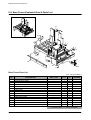
Disassembly and Reassembly
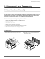
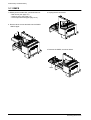
3. Disassembly and Reassembly
3-1 General Precautions on Disassembly
When you disassemble and reassemble components, you must use extreme caution.
The close proximity of cables to moving parts makes proper routing a must. If components are removed, any
cables disturbed by the procedure must be restored as close as possible to their original positions. Before
removing any component from the machine, note the cable routing that will be affected.
Whenever servicing the machine, you must perform as follows:
1. Check to verify that documents are not stored in memory.
2. Unplug the power cord.
3. Use a flat and clean surface.
4. Replace only with authorized components.
5. Do not force to remove or planten plastic-material components.
6. Make sure all components are in their proper position.
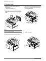
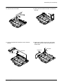
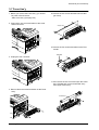
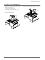
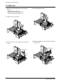
3-2 Rear Cover
1. Remove the six screws securing the Rear Cover.
Samsung Electronics
2. Separate the rear cover from the base frame
and Scanner Ass'y.
3-1
Disassembly and Reassembly
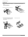
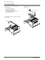
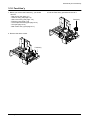
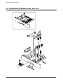
3-3 Scanner Ass'y
1. Before you remove the Scanner Ass'y, you
should remove:
- Rear Cover (see page 3-1)
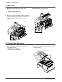
4. Open the Side Cover assembly first to open the
Front cover. In the other words, close the front
cover first to assembly it.
.
2. Remove the six screws and take out the Shield
Main Upper.Unplug the one connector and CCD
cable.
Side Cover Ass’y
Shield Main Upper
2
1
Front Cover
Notice :
You should connector remove the CCD cable vertically to
avoid the CCD cable pin damage.
5. Remove two screws.
3. Remove the three screws, as shown below.
3-2
Samsung Electronics
Disassembly and Reassembly
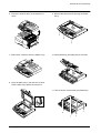
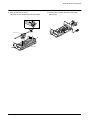
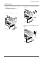
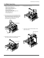
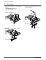
6. Pull up the Scanner Ass'y in the direction of
arrow.
9. Remove the three screws securing the Platen
Ass'y.
7. Remove the connector from the Platen Ass'y.
10. Pull the OPE Ass'y and unplug the one connector.
8. Open the ADF Ass’y in the direction of arrow.
Pull the ADF Ass'y upward and remove it.
11. Remove the five screws securing the Platen Ass'y.
Samsung Electronics
3-3
Disassembly and Reassembly
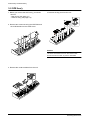
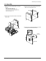
12. Unlatch the Scan Upper Ass'y securing the
glass and remove it.
14. Remove the four screws and Channel Base
Frame.
Channel Base Frame
Notice :
When foreign material enters into the Scan Assy, it may
cause problems in product performance and deteriorate
scan image. Therefore, you should always dismantle or
assemble it at a clean place.
13. Remove the two scews and pull the Dummy
Upper Ass’y.
15. Remove the five screws and Dummy ScanLower.
Dummy Upper Ass’y
Cover Dummy Lower
Cover Scan Lower
3-4
Samsung Electronics
Disassembly and Reassembly
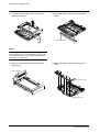
16. Remove the CCD cable.
18. Remove three screws and take out the Motor
Bracket.
17. Pull up the Shaft CCD and take out the Scanner
Module.
19. Remove the OPE Harness from the Platen
PBA. Remove two screws and take out the
Platen PBA.
Platen PBA
Shaft CCD
OPE Harness
Pully
Scanner Module
Belt
Samsung Electronics
3-5
Disassembly and Reassembly
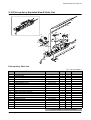
3-4 ADF Ass'y
1. Before you remove the ADF Ass'y, you should
remove:
- Rear Cover (see page 3-1)
- Scanner Ass'y (see page 3-2)
4. Pull the ADF Ass'y upward and remove it.
2. Remove the five screws from the Platen Cover.
Platen Cover Ass’y
Platen Cover Ass’y
3. Open the Cover open and pull the Cover Side L
and Cover Side R and unlatch the Side Cover L
by pushing the part hooked the Platen Cover
using a sharp tool.
5. Tack out he Open Cover.
Side Cover R
Side Cover L
Cover Open
Platen Cover Ass’y
3-6
Samsung Electronics
Disassembly and Reassembly
6. Take out the Pick-up Ass’y.
Remove the four screws and the ADF Upper.
7. Remove three screws and take out the ADF
Motor ass'y.
Pick-up Ass’y
ADF Upper
Samsung Electronics
3-7
Disassembly and Reassembly
3-5 OPE Ass'y
1. Before you remove the OPE Ass'y, you should
remove:
- Rear Cover (see page 3-1)
- Scanner Ass'y (see page 3-2)
4. Remove the key pad from the unit.
2. Remove ten screws securing the OPE PBA and
the LCD Module from the OPE Cover.
Caution
The above information is for the SCX-5312 model.
For the SCX-5112 model, “A” parts is eliminated.
3. Remove the contact rubbers from the unit.
3-8
Samsung Electronics
Disassembly and Reassembly
3-6 Side Cover Ass'y
1. Remove the two screws to release the Stopper(Main Frame side) securing the Side Cover
to the Main Frame.
* MP-Tray
1. Pull the both side of the
part to dissemble it.
1
1
2. Completely open the Side Cover Ass’y, and
after pull the
part to the arrow direction (to
the top), pull the
part to the arrow direction
(inner side).
2. As the
part, make the Tray-Case and the
Tray-Link in rectangular position to dissemble
the Tray-Case from the Tray Link. The Tray Link
locates at an angle of 45˚ from the Side Cover
Ass’y and then remove the Tray Link.
MP Tray
2
2
3
1
1
Tray Link
Samsung Electronics
Tray-Case
3-9
Disassembly and Reassembly
* Duplex Ass’y
* Transfer Roller Ass’y
1. Unite the
part and home to the projection
part of the Side Cover assembly, and widen
them from each other to dissemble the Side
Cover Ass’y.
1. Take out the Transfer Roller, as shown below.
Deplex Ass’y
3-10
Samsung Electronics
Disassembly and Reassembly
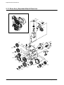
3-7 Fuser Ass'y
1. Before you remove the Fuser Ass'y, you should
be power off and remove:
- Side Cover Ass'y (see page 3-9)
2. Remove the one screw and take out the Cover
Sheet Connector.
6. Remove the two screws and take out the Halogen Lamp.
Halogen Lamp
5. Remove the four screws and take out the Thermostat.
Thermostat
3. Unplug the one connector.
7. After remove the two screw and open the Lower
Ass’y froward tack out the Heat Roller Ass’y
from Upper Fuser Ass’y.
4. Remove the three screws and take out the Fuser
Ass'y.
Heat Roller
Samsung Electronics
3-11
Disassembly and Reassembly
3-8 Exit Ass'y
1. Before you remove Exit Ass'y, you should
remove:
- Rear Cover (see page 3-1)
- Scanner Ass'y (see page 3-2)
3. Pull the exit ass’y and remove it.
2. Remove four screws, and then untile the harness
from the Exit Upper. Unplug four connectors and
unlatch the Dummy Base Frame, as shown
below.
3-9 Cover Paper Exit Ass'y
1. Before you remove the Cover Paper Exit Ass'y,
you should remove:
- Rear Cover (see page 3-1)
- Scanner Ass'y (see page3-2)
2. Remove two screws and Cover Paper Exit Ass'y,
as shown below.
Cover Paper Exit Ass’y
3-12
Samsung Electronics
Disassembly and Reassembly
3-10 Drive Ass'y
1. Before you remove the Drive Ass'y, you should
remove:
- Rear Cover (see page 3-1)
- Shield Main Upper (see page 3-2)
3. Remove the one screw and take out the Fan and
Dust Fan.
2. Unplug the two connectors.
(Main Motor:9pin, Duplex Solenoid : 2pin)
Fan
Dust Fan
4. Remove the five screws and take out the Drive
Ass'y.
Drive Ass’y
Samsung Electronics
3-13
Disassembly and Reassembly
3-11 SMPS
1. Before you remove the LSU, you should remove:
- Rear Cover (see page 3-1)
- Scanner Ass'y (see page 3-2)
- Cover Paper Exit Ass’y(see page 3-12)
3. Unplug the all connectors.
2. Remove three screws and take out the Shield
SMPS Upper.
4. Remove the SMPS, as shown below.
SMPS
3-14
Samsung Electronics
Disassembly and Reassembly
3-12 LSU (Laser Scaning Unit)
1. Before you remove the LSU, you should remove:
- Rear Cover (see page 3-1)
- Scanner Ass'y (see page 3-2)
- Cover Paper Exit Ass’y (see page 3-12)
3. Remove the three screws and take out the LSU.
LSU
2. Unplug the two connectors.
Samsung Electronics
3-15
Disassembly and Reassembly
3-13 Cover Exit Rear
1. Before you remove the Cover Exit Rear, you
should remove:
- Rear Cover (see page 3-1)
- Scanner Ass'y (see page 3-2)
- Exit Ass'y (see page 3-12)
- Cover Paper Exit Ass’y(see page 3-12)
- SMPS (see page 3-14)
3. Remove the one screw and Cover Exit Rear, as
shown below.
Cover Exit Rear
2. Remove the one screw and take out the Panel
Connect MPF.
3-16
Samsung Electronics
Disassembly and Reassembly
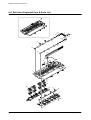
3-14 Main Frame Ass'y
1. Before you remove the LSU, you should remove:
- Rear Cover (see page 3-1)
- Scanner Ass'y (see page 3-2)
- Side Cover Ass'y (see page 3-9)
- Fuser (see page 3-11)
- Exit Ass'y (see page 3-12)
- Cover Paper Exit Ass’y(see page 3-12)
- SMPS (see page 3-14)
- LSU (see page 3-15)
4. Unplug the all connectors.
2. Remove one screw in the Channel Base Frame
from the bellow section of the Base Frame, and
then remove the rest of the five screws to dissemble the Dummy Base Frame, the Cover
Front and the Cam Jam Remove.
Dummy Base Frame
Cam Jam Remove
5. Remove the seven screws and take out the
Main Frame Ass'y.
Main Frame Ass’y
Front Cover
3. Remove the Locker Deve, and then remove the
one screw and the Cover Motor Bracket.
Cover Motor Bracket
Lock Deve
Samsung Electronics
3-17
Disassembly and Reassembly
3-15 MP Ass'y
1. Before you remove the MP Ass’y, you should
remove:
- Rear Cover (see page 3-1)
- Shield Main Upper (see page 3-2)
- Side Cover Ass'y (see page 3-9)
4. remove the three screws.
2. Unplug the two connectors.
3. Remove the one screw and take out the Dummy
Cover.
5. Release the SMPS fit. Pull the MP Ass'y upward
and remove it.
MP Ass’y
Dummy Cover
3-18
Samsung Electronics
Disassembly and Reassembly
3-16 Feed Ass'y
1. Before you remove the Feed Ass’y, you should
remove:
- Rear Cover (see page 3-1)
- Scanner Ass'y (see page 3-2)
- Side Cover Ass'y (see page 3-9)
- Exit Ass'y (see page 3-12)
- Cover Paper Exit Ass’y(see page 3-12)
- LSU (see page 3-15)
- Main Frame Ass’y (see page 3-17)
3. Pull the Feed Ass'y upward and remove it.
Feed Ass’y
2. Remove the three screws.
Feed Ass’y
Samsung Electronics
3-19
Disassembly and Reassembly
3-17 Pick Up Ass'y
1. Before you remove the Pick Up Ass’y, you should
remove:
- Rear Cover (see page 3-1)
- Shield Main Upper (see page 3-2)
- Drive Ass'y (see page 3-13)
4. Remove the four screws and take out the Pick Up
Ass'y, as shown below.
2. Unplug the three connectors.
Guide Paper Out
3. Remove the two screws and take out the Cassette Rail.
Pick-up Ass’y
Cassette Rail
3-20
Samsung Electronics
Disassembly and Reassembly
3-18 Main PBA
1. Before you remove the Main PBA, you should
remove:
- Rear Cover (see page 3-1)
- Side Cover Ass'y (see page 3-9)
- Cover Paper Exit Ass’y(see page 3-12)
- SMPS (see page 3-14)
3. Remove the five screws and take out the main
PBA from the Shield Main Lower.
Main PBA
2. Remove the two screws and take out the Shield
Main Lower.
Shield Main Lower
4. Remove the one screw and unlatch the LIU PBA
securing the main PBA and remove it.
LIU PBA
(Only SCX-5312F)
Main PBA
Samsung Electronics
3-21
Troubleshooting
4. Maintenance & Troubleshooting
In this chapter, it was mentioned about the functions for maintaining the product, how to find the causes of the
inferiority, and troubleshooting method.
The service manual is bound the SCX-5312F and SCW-5112 together in one volume.
The SCX-5312F has functions such as printer, copy, scanner, and fax. The SCX-5112 has all functions as the
SCX-5312F but the fax function.
The contents of the manual are standardized for the SCX-5312F.
The information about the fax function is not applied for the SCX-5112.
The differences by each model are explained in a separate way.
4-1 Preventative Maintenance
The cycle period outlined below is a general guideline for maintenance.
The example list is for an average usage of 50 transmitted and received documents per day.
Environmental conditions and actual use will vary these factors.
The cycle period given below is for reference only.
Samsung Electronics
COMPONENT
REPLACEMENT CYCLE
ADF Rubber
20,000 Pages
ADF Roller
50,000 Pages
Pick-up Roller
75,000 Pages
Transfer Roller
75,000 Pages
Fuser
75,000 Pages
Toner Cartridge
6,000 Pages
Drum Cartridge
15,000 Pages
4-1
Troubleshooting
4-2 Error Messages
Error Message
Description
Solution
RETRY REDIAL?
The machine is waiting for the programmed interval to automatically redial.
You can press START to immediately
redial, or STOP to cancel the redial
operation.
COMM. ERROR
A problem with the facsimile communications has
occurred.
Try again.
DOCUMENT JAM
Loaded document has Jammed in the feeder
When Document Jam aeeurred at ADF module
Clear the document Jam.
DOOR OPEN
The side cover is not securely latched.
Clear the cover until it clicks in place.
GROUP NOT AVAILABLE
You have tried to select a group location where
only a single location number can be used, such
as when adding locations for a multi-dial operation.
Try again, check location for group.
LINE ERROR
Your unit cannot connect with the remote
machine, or has lost contact because of a problem on the phone line. When the mechine has a
problem in cause of fax data reception step
Try again. If failure persists, wait an
hour or so for the line to clear then try
again.
LOAD DOCUMENT
You have attempted to set up a sending operation with no document loaded.
Load a document and try again.
MEMORY FULL
The memory has become full.
Either delete unnecessary documents, or
retransmit after more memory becomes
available, or split the transmission into
more than one operation.
NO ANSWER
The remote machine was not answered after all
the redial attempts.
Try again.
Make sure the remote machine is OK.
NO. NOT ASSIGNED
The speed dial location you tried to use has no
number assigned to it.
Dial the number manually with the keypad, or assign the number.
NO PAPER
[ADD PAPER]
The recording paper has run out. The printer system stops.
Load the recording paper in the paper
feeder.
OVERHEAT
The printer part has overheated.
Your unit will automatically return to the
standby mode when it cools down to normal operating temperature. If failure persists, call service.
PAPER JAM 0
OPEN/CLOSE DOOR
Recording paper has jammed in paper feeding
area.
Recording paper is jammed in pick-up unit
Press STOP and clear the jam.
PAPER JAM 1/2
OPEN/CLOSE DOOR
Recording paper has jammed inside the unit.
Recording paper has jammed in paper exit unit.
Clear the jam.
TONER LOW
Toner may be low
Toner may be unevenly distributed.
Remove the toner cartridge and shake it
gently to evenly distribute the toner. Then
replace the toner cartridge.
TONER EMPTY
When the machine has encountered the Toner
Empty.
Replace the Toner Cartridge.
DRUM WARNING
When the machine has encountered the drum
life,14000 print pages.
Use little more change if “REPLACE
DRUM” is marked in LCD window.
REPLACE DRUM
When the machine has encountered the out of
from lifr, 15000 print pages.
Replace the Drum Cartridge.
4-2
Samsung Electronics
Troubleshooting
Error Message
Description
Solution
NO CARTRIDGE
When the machine detected the toner cartridge
has not been installed.
Install the Cartridge.
BYPASS JAM
When the machine detected the non-feeding from
BYPASS Tray.
Open the side Cover and clear the jam.
DUPLEX JAM
When the machine detected the duplex jam in the
middle of machine.
Clear the jam.
LINE BUSY
The remote FAX didn’t answer
Try again.
OPEN HEAT EROR
Thermister does not connected to main board or
contact point is not coupled tightly in power on.
Check thermister contact point, Heating
Camp & Thermostat.
Heating Error
During operation, Temperatare does not go up.
Check thermister contact point & Heating
Lamp.
Scanner Locked
Scanner is locked by locker.
Check locker.
Connect the Flat-Cable.
Samsung Electronics
4-3
Troubleshooting
4-3 User Mode
The table in the bellow explains the possible setting functions by user. The details about the ways to use are
explained in the user manual.
In the service manual, the items are about the possible set-up by user.
4-3-1 SCX-5312F
Function
SYSTEM DATA
SYSTEM ID
Item
Content
CASSETTE PAPER
LETTER / A4 / LEGAL
BYPASS PAPER
LETTER / A4 / LEGAL
MESSAGE CONF.
ON / OFF / ERROR
AUTO JOURNAL
ON / OFF
RECEIVE CODE
0-9
POWER SAVE
ON / OFF
ECM MODE
ON / OFF
RX REDUCTION
ON / OFF
DISCARD SIZE
0-30mm
REDIAL INTERVAL
1-15
REDIALS
1-13
ANSWER ON RING
1-7
SEND FROM MEMORY
ON / OFF
LOCAL ID
ON / OFF
CLOCK MODE
12 / 24 HOUR
FAX / ID
DATE & TIME
SYSTEM SETUP
MEMORY CLEAR
PREFIX DIAL NO.
RINGER VOLUME
LOW / HIGH (10 STEPS)
ALARM SOUND
ON / OFF
KEY SOUND
ON / OFF
SPEAKER CONTROL
COM / ON /OFF
SELECT LANGUAGE
ENG/GER/FRE/ITA/SPA/POR/DUT
USB MODE
FAST / SLOW
FAX DUPLEX
OFF / LONG EDGE / SHORT EDGE
IMAGE QUALITY
NORMAL / TEXT / IMAGE
SYSTEM ID
SYSTEM DATA
PHONE BOOK / MEMORY
TX-RX JOURNAL
DELAY TX
MEMORY TX
PRIORITY TX
POLLING
ADD/CANCEL
ADD / CANCEL
GROUP DIAL
MAINTENANCE
CLEAN DRUM
NEW DRUM
NOTIFY TONER LOW
4-4
ON / OFF
Samsung Electronics
Troubleshooting
Function
Item
Content
TX CONFIRM
SCHEDULE JOB
PHONE BOOK
SYSTEM LIST
TX JOURNAL
RX JOURNAL
HELP LIST
HELP LIST
4-3-2 SCX-5112
Function
SYSTEM DATA
Item
Content
CASSETTE PAPER
LETTER / A4 / LEGAL
BYPASS PAPER
LETTER / A4 / LEGAL
POWER SAVE
ON / OFF
SELECT LANGUAGE
ENG/GER/FRE/ITA/SPA/POR/DUT
USB MODE
FAST / SLOW
HELP LIST
HELP LIST
PRINTOUT
MAINTENANCE
CLEAN DRUM
NEW DRUM
REPORTS
SYSTEM DATA
HELP LIST
HELP LIST
4-4 Tech Mode
4-4-1 How to Enter Service Mode
In service mode (tech) mode, the technician can check the machine and perform various test to isolate the
cause of a malfunction.
To enter the Tech mode, press MENU, #, 1, 9, 3, 4 in sequence, and the LCD briefly displays ‘T’, the
machine has entered service (tech) mode.
While in Tech mode, the machine still performs all normal operations.
To return to normal user mode, press MENU, #, 1, 9, 3, 4 in sequence again, or turn the power off, then on
by unplugging and plugging the power cord.
Options changed while in service mode do not remain changed unless you clear the machine’s memory.
Samsung Electronics
4-5
Troubleshooting
4-4-2 Setting-up System in Tech Mode
4-4-2-1 SCX-5312F(SETUP : #, 1, 9, 3, 4)
Function
SYSTEM DATA
Item
DIAL MODE
Content
TONE / PULSE
MODEM SPEED
ERROR RATE
5% /10%
SET TX LEVEL
09-15
SILENCE TIME
12 / NU / OFF
SYSTEM ID
The same as User Mode
DATE & TIME
The same as User Mode
SYSTEM SETUP
The same as User Mode
MEMORY CLEAR
CLEAR ALL MEMORY
DELAY TX
The same as User Mode
MEMORY TX
The same as User Mode
PRIORITY TX
The same as User Mode
POLLING
The same as User Mode
ADD/CANCEL
The same as User Mode
GROUP DIAL
The same as User Mode
MAINTENANCE
CLEAN DRUM
NEW DRUM
NOTIFY TONER LOW
ON / OFF
SWITCH TEST
MODEM TEST
SRAM TEST
DRAM TEST
ROM TEST
FLASH / ENGINE
PATTERN TEST
PATTERN1-7, QAPATTERN1-4, ALL"1-7 , ALL"
CLEAR COUNT
PASSWORD
CRU PRINTS COUNT
FLT SCAN COUNT
ADF SCAN COUNT
USED DRUM COUNT
USED TONER COUNT
TOTAL PAGE COUNT
ANSWER ON CNG
1-4
ADJUST SHADING
FLASH UPGRADE
LOCAL
REMOTE : USER PROGRAM ,
EMULATION ,BOOT PROGRAM
PROGRAM DIAL
TX CONFIRM
The same as User Mode
SCHEDULE JOB
The same as User Mode
PHONE BOOK
The same as User Mode
SYSTEM LIST
USER MODE
TX JOURNAL
The same as User Mode
RX JOURNAL
The same as User Mode
4-6
Samsung Electronics
Troubleshooting
Function
REPORTS
Item
Content
MSG. CONFIRM
SCHEDULE JOB
PHONE BOOK
SYSTEM DATA
TRANSMISSION
RECEPTION
HELP LIST
PROTOCOL
ERROR CODE
4-4-2-2 SCX-5112(SETUP : #, 1, 9, 3, 4)
Function
SYSTEM DATA
MAINTENANCE
Item
Content
CASSETTE PAPER
LETTER / A4 / LEGAL
BYPASS PAPER
LETTER / A4 / LEGAL
POWER SAVE
ON / OFF
SELECT LANGUAGE
ENG/GER/FRE/ITA/SPA/POR/DUT
USB MODE
FAST / SLOW
CLEAN DRUM
MODEM TEST
NEW DRUM
SWITCH TEST
SRAM TEST
DRAM TEST
ROM TEST
FLASH / ENGINE
PATTERN TEST
PATTERN1-7, QAPATTERN1-4 , ALL
CLEAR COUNT
PASSWORD
CRU PRINTS COUNT
FLT SCAN COUNT
ADF SCAN COUNT
USED DRUM COUNT
USED TONER COUNT
TOTAL PAGE COUNT
ADJUST SHADING
FLASH UPGRADE
REPORTS
SYSTEM DATA
HELP LIST
HELP LIST
ERROR CODE
Samsung Electronics
4-7
Troubleshooting
4-4-3 SYSTEM DATA
DIALING MODE
Select the dialing mode according to the user's line status.
TONE: Electrical type of dial
PULSE: Mechanical type of dial
SILENCE TIME
In ANS/FAX mode, after a call is picked up by the answering machine, the machine monitors the line. If a
period of silence is detected on the line at any time, the call will be treated as a fax message and the machine
begins receiving.
Silence detection time is selectable between limited (about 12 seconds) and unlimited time.
When '12 sec' is selected, the machine switches to receiving mode as soon as it detects a period of silence.
When 'unlimited'is selected, the machine waits until the answering operation is concluded even though a
period of silence is detected. After the answering operation is concluded, the machine switches to receiving
mode.
SEND FAX LEVEL
You can set the level of the transmission signal. Typically, the Tx level should be under -12 dBm.
Caution: The Send Fax Level is set at the best condition in the shipment from factory. Never change
settings arbitrarily.
ERROR RATE
When the error rate is about to be over the setting value, the Baud rate automatically lowers up to 2400 bps to
make the error rate remain below the setting value.
You can select the rate between 5% and 10%.
MODEM SPEED
You can set the maximum modem speed.
Communication is done with modem speed automatically set at lower speed when communicating with the
modem with lower speed since communication is done on the standard of the side where modem speed is low
for transmission/reception. It is better set 33.6Kbps as default setting.
4-4-4 MEMORY CLEAR
CLEAR ALL MEMORY
The function resets the system as its very first condition as setting in at the factory.
This function is needed to operate to reset the system to the initial value when the product is abnormally operated or malfunction. All the values are returned to the default values, and all the information, which set in by
user, will be erased.
< Method >
1. Select the [MEMORY CLEAR] at the TECH MODE.
2. Push the ENTER button.
3. Select you country.
4. Push the ENTER button then it will be all memory clear. .
NOTICE : Always perform the memory clear after replace the main board. Otherwise, the system may
not operate properly.
4-8
Samsung Electronics
Troubleshooting
4-4-5 MAINTENANCE
CLEAN DRUM
Use this feature to get rid of the toner remained in the development unit, so you can get a clean printout.
Perform this feature if stains or specks appear on the printing materials and print quality falls.
Perform this feature several times until a clean printing material appears.
The machine automatically pulls in a sheet of paper,and prints out.The toner particles on the OPC drum surface is fixed to the paper.
FLASH UPGRADE
It is Firmware Upgrade function and has two methods, Local and Remote.
More information can be found in the firmware upgrade items.
ADJUST SHADING
The function is to control to get the optimum scan quality by the specific character of the CCD(Charge Coupled Device). If the copy image quality is unsatisfied, perform the function to check the condition of the print
out for checking whether or not having CCD trouble.
< Method >
1. Select the [ADJUST SHADING] at the TECH MODE.
2. Push the SET UP button then an image will be scanned.
3. After the scan, CCD SHADING PROFILE will be print out.
4. If the printed image is different to the image, the CCD is defect.
NOTICE : When you test CCD, make sure
that the cover is closed.
ANSWER ON CNG
The function is to control the CNG TONE cognition times for entering receiving mode from the AUTO MODE
or ANS/FAX MODE
Samsung Electronics
4-9
Troubleshooting
CLEAR COUNT
This function erases information of history such as replacement times of Developing part and OPC drum,
total printing pages, scan times, and etc.
- The items are in the below section of the System Data List, printed at TECH MODE.
- PASSWOEED: 1934
- Current Drum Page Count cannot be erased.
It is possible to erase at NEW DRUM function (USER MODE ⇒ MINTENANCE ⇒ NEW DRUM)
FIRMWARE VERSION
ENGINE VERSION
EMULATION VERSION
:
:
:
TOTAL PAGE COUNTS
CRU PRINTS
REPLACED TONER COUNTS
REPLACED DRUM COUNTS
CURRENT DRUM COUNTS
PLATEN SCAN PAGE COUNTS
ADF SCAN PAGE COUNTS
:
:
:
:
:
:
:
1.00
1.00
PCL6 2.32 07-11-2001
PCL5e 1.48 07-19-2001
123
123
1
1
112
23
10
< SYSTEM DATA LIST >
PATTERN TEST
Using this pattern printout, you can check if the printer mechanism is functioning properly.
It is needed in the production progress. Service person doesn't need to use it.
ROM TEST
Use this feature to test the machine'S ROM. The result and the software version appear in the LCD display.
• FLASH VER : 1.00 V
• ENGINE VER :1.00V
DRAM TEST
Use this feature to test the machine's DRAM. The result appears in the LCD display.
If all memory is working normally, the LCD shows << O K >>
SRAM TEST
Use this feature to test the machine's SRAM. The result appears in the LCD display.
If all memory is working normally, the LCD shows << O K >>
MODEM TEST
Use this feature to hear various transmission signals to the telephone line from the modem and to check the
modem. If no transmission signal sound is heard, it means that the modem part of the main board is poor.
SWITCH TEST
Use this feature to test all keys on the operation control panel. The result is displayed on the LCD window
each time you press a key.
4-10
Samsung Electronics
Troubleshooting
NOTIFY TONER LOW
With this feature enabled, when the toner becomes low, the toner low information will be sent to ta specified
contact point, for example, the service company. After you access this menu, select ON, and when the LCD
prompts, enter the name and the number of the contact point, the customer's fax number, the model name,
and the serial number.
PROGRAM DIAL
It is a function setting transmitting conditions to transmit to specific address preliminary.
When user transmit specific address set this function, the conditionsapplied automatically.
4-4-6 REPORT/HELP
MSG. CONFIRM
It shows the result of the last send operation.
PROTOCOL LIST
This list shows the sequence of the CCITT group 3 T.30 protocol during the most recent sending or receiving
operation. Use this list to check for send and receive errors. If a communication error occurs while the
machine is in TECH mode, the protocol list will print automatically.
Facsimile Information Field
data described in hexdecmal code
Sending/Receiving
Name of signal
(Facsimile Control Field)
FIF data described
in ASCII code
PROTOCOL DUMP LIST
S/R FCF
S
S
S
S
S
S
R
R
S
R
R
S
R
S
S
FIF DATA
NOV-20-2001
ASCII
NSF 61005820003380140200001302090018010000
CSI 2020202020202020202020202O20202020202020
DIS 00000000 01110111 00010111 00100010
NSF 61005020003380140200001302090018010000
CSI 202020202020202020202022O202020220202020
DIS 00000000 01110111 00010111 00100010
TSI 2020202020202020202020202O20202020202020
DCS 00000000 01100001 00010101 00000000
FTT
TSI 2020202020202020202020202O20202020202020
DCS 00000000 01100001 00010101 00000000
CFR
MPS
MCF
DCN
HELP
It shows a brief description on the machine's basic functions and commands.
Use it as a quick reference guide
Samsung Electronics
4-11
Troubleshooting
RECEPTION
This journal shows a specific information concerning reception activities, the time and dates of up to 40 of the
most recent receptions.
TRANSMISSION
This journal shows a specific information concerning transmission activities, the time and dates of up to 40 of
the most recent transmissions.
SYSTEM DATA
This list provides a list of the user system data settings and tech mode settings.
PHONEBOOK
It lists all telephone numbers that have been stored in the machine.
SCHEDULE JOB
This list shows a specific information on the documents currently stored for delayed transmission. It provides
the operation number, starting time, type of operation, etc.
ERROR CODE
It shows error history occurred using product.
4-4-7 Firmware Upgrade
It is a new Firmware, and there are two Upgrade methods by local and remote.
4-4-7-1 Local Machine
RCP(Remote Control Panel) mode
This method is for Parallel Port.or USB Port Connect to PC and activate RCP(Remote Control Panel) to
upgrade the Firmware.
< Method >
How to Update Firmware using RCP
1. Connect PC and Printer with Parallel Cable or USB Cable.
2. Execute RCP and select Firmware Update. Current Firmware version and Emulation Version are displayed
on Current version window.
3. Search Firmware file to update with Browse Icon.
4. Click Update icon, firmware file is transmitted to Printer automatically and printer is initialized when it finished.
5. Click Refresh icon and check what is updated.
4-12
Samsung Electronics
Troubleshooting
DOS Command mode
This method is just for Parallel Port. Connect to PC with Parallel cable and enter DOS Command to upgrade
the Firmware.
< Method >
a). The first of all, need the files : down.bat, down_com.bin, fprt.exe, and Rom File: file name for upgrade.Save the files in the
same folder.
b). In the DOS, input as below and push the enter key. Then, it will be automatically upgraded.
c) There are two commands for the conditions of product.
* When the product is in idle condition
down "rom file"
* When the product is in idle condition(TECH MODE → MAINTENANCE → FLASH UPGRADE →LOCAL)
fprt "rom file"
d) Do not turn off the power while upgrading process.
4-4-7-2 Remote FAX
This is a function that a fax with the latest firmware sends files to a fax in long distance through telephone line.
< Method >
1. Operate a fax with the latest firmware to prepare it being upgrade.
(TECH MODE MAINTENANCE FLASH UPGRADE REMOTE)
2. Input the fax number, which needs to be upgraded.
(Several faxes can be upgrade at the same time. In this case, enter the each fax number.)
3. After push the enter button, send the firmware file by calling to the appointed number.
(Around 10~15 minutes needs to send the file.)
< Caution >
1. sending and receiving fax must be the same model.
2. A sending fax must be set up as ECM mode, and a receiving memory must be set up as 100%.
If not, the function operates abnormally.
4-4-8 Identify Sale Date(Only SCX-5312F)
This function confirms the date that consumer buys product and use product by first actually.
If make consumer buy and operate the machine, the machine recognize the first Scan page count, Print page
count etc.
The time is remembered to first machine use event.
< Method >
These contents are remembered continuously after memory delete (Clear All Memory).
Method : Press MENU, #, 1, 9, 3, # in sequence.Firmware version is displayed on LCD.
FLASH VER : 1.00
ENGINE VER : 1.00
Press 1( in the number keypad) : The LCD display shows "Updated date"
Press 2( in the number keypad) : The LCD display shows "Product first use date"
Samsung Electronics
4-13
Troubleshooting
4-5 ENGINE TEST MODE
The Engine Tests Mode supplies useful functions to check conducting condition of engine. It tests the conducting condition of each device and displays the result of the test at the LCD. It is classified in 6. items (0~5),
and the functions of items are as bellows.
4-5-1 To enter the Engine Test Mode
Press MENU, #, 1, 9, 3, 1 in sequence, and the LCD briefly displays ‘T’, the machine has entered service
(tech) mode.
4-5-2 Diagnostic
Remark
No .
Sub No .
0
1
Motor Test
1: On,
2: Off
2
PTL T est
1: On,
2: Off
3
F an T es t
1: On,
2: Off
4
F us er Test
1 : On, 2: Off
If its temperature is lower than the Standby
(160 C), the fuser is on, but if it is higher than
the Standby, the fuser is off.
1
LSU Motor Test
1: On,
2: Off
2
LSU Hsy nc Test
1: On,
2: Off
3
LD On Test
1: On,
2: Off
4
LSU Operation
1: On,
2: Off
1
F eed Sensor T es t
Sensor O n : FEED SENSOR ON Display
1
2
Eng ine test
Sensor O ff : FEED SENSOR OFF Display
2
Exit Sensor Test
3
Cov er Sensor T es t
4
1’st CAST Empty Test
Sensor O n : EXIT SENSOR ON Display
Sensor O ff : EXIT SENSOR OF F Display
Sensor O n : COVER SENSOR ON Display
Sensor O ff : COVER SENSOR OFF Display
Sensor O n : 1’s t PAPER Empty Display
Sensor O ff : 1’s t PAPER No Empty Display
5
MP Empty Sen T est
Sensor O n : MP PAPER Empty Dis play
6
BIN FULL Sen TEST
1
1’st CAST Solenoid Test
1: On,
2: Off
2
MP Solenoid Test
1: On,
2: Off
3
Duplex Solenoid T es t
1: On,
2: Off
1
MHV Test
1: On,
2: Off (-1450v)
2
Dev Bias Test
1: On,
2: Off (-450v)
3
T HV EN/NEG T es t
1: On,
2: Off
4
T HV T es t
1: On,
2: Off (1300v)
5
T HV T rigger T est
1: On,
2: Off
All Function Test
F or SMD T est, Pus h up k ey : Next function
All Function : No.0~4
Sensor O ff : MP PAPER No Empty Display
Sensor O n : BIN F ULL SEN ON Display
Sensor O ff : BIN F ULL SEN O FF Display
3
4
5
1
4-5-3 ENGINE PRINT
When the function is on, sentence to explain the condition of engine is printed in the below section of the printing output.
4-14
Samsung Electronics
Troubleshooting
It is needed in the development progress. Service person doesn't need to use it.
4-6 Troubleshooting
4-6-1 Scanner
4-6-1-1 COPY
PROBLEM
White copy
Black copy
Defective image quality
Abnormal noise
Samsung Electronics
ITEMS TO BE CHECKED.
HOW TO SOLVE
• Check the Scan-Cover open.
• Room light can transit a thin original.
• Check shading profile.
• Remake shading profile in the tech mode.
• Check white/black reference voltage in
Main PBA.
• Replace U16 if it is defective.
- U16-97 = 2.5V - U16-98 = 3.3V
- U16-99 = 1.5V
• Check turning the CCD Lamp on when
operating.
• If the CCD is defective, replace it.
- CN3-19 is 5.8V when white original copying for R, B and 3.5V for G.
• Check the CCD problem in Main PBA.
• Check the CCD harness contact.
• Check shading profile.
• Remake shading profile in the tech mode.
• Check the CCD problem in Main PBA.
• If the CCD is defective, replace it.
- Cn3-19 is 7.3V when idle for R, B, and 5V
for G.
• Check shading profile.
• Remake shading profile in the tech mode.
• Check the gap between original and scanner glass.
• The gap above 0.5mm can cause a
blurred image.
• Check printing quality.
• See “Print” troubleshooting.
• Check the Scanner Motor and any
mechanical disturbance.
• Check the right position of the Scanner
Motor, and check the any mechanical disturbance in the CCD carriaging part.
• Check the Motor Driver in Driver PBA.
• If any driver is defective, replace it.
- U55-1 or U55-15 = 0V to 24V swing signal
when operating.
4-15
Troubleshooting
4-6-1-2 PC-Scan
PROBLEM
Scanning Error
Defective image
Quality
Abnormal noise
4-16
ITEMS TO BE CHECKED.
HOW TO SOLVE
• Check the printer cable installed.
• Check correct installation, and use standard IEEE1284 cable.
• Check how TWAIN driver is installed.
• Remove any other scanner driver.
• Reboot after reinstallation of the TWAIN
driver.
• Check the printer port(Parallel).
• Check the parallel-port-related items in the
CMOS Setup.
As a printer port, Select ECP among
SPP(Normal), ECP, and EPP
modes(increase print-ing speed)
• Check harness contact.
.
• Check CN14 contact in Main PBA
• Check the IEEE1284 signal level.
• If any signal level is defective, replace
Driver PBA.
- U36-66~74 in Main PBA = 0.8V to 2.4V
TTL signal.
• Otherwise, replace Main PBA.
• Check the USB signal level.
• If USB signal level is defective, replace
Main PBA.
• Check shading profile.
• Remake shading profile in the tech mode.
• Check the gap between original and scanner glass.
• The gap above 0.5mm can cause a
blurred image.
• Check the Scanner Motor and any
mechanical disturbance.
• Check the right position of the Scanner
Motor, and check the any mechanical disturbance in the CCD carriaging part.
• Check the motor driver in Driver PBA.
• If any driver is defective, replace it.
- U55 or U56-1 = 0V to 24V swing signal
when operating.
Samsung Electronics
Troubleshooting
4-6-2 FAX(only SCX-5312F)
4-6-2-1 FAX/TELEPHONE Precautions
PROBLEM
TEL LINE CANNOT BE
ENGAGED
(NO DIAL TONE)
ITEMS TO BE CHECKED.
• When you press “ OHD” key:
a) Check line cord connection.
b) Check MAIN LIU harness, and CN1
(LIU PBA).
c )Check relay operation of LIU PBA :
Is the control signal of CN20-7(main) low?
HOW TO SOLVE
a) insert it correctly into the connection
jack called “line”.
b) Replace defective parts.
c) Replace main PBA IF the control signal
of CN20-7(main) is high.
Replace LIU PBA if high but phone line
cannot be connected.
Cannot MF dial
• Check CN20 (main PBA), MAIN-LIU
harness, and CN1 (LIU PBA)
• Replace defective parts.
MF dial is possible but
not DP dial.
• Check DP control signal of CN20-11 of
MAIN PBA and the circuit around R15. U6
and Q2 of Liu PBA.
• Replace LIU PBA.
Defective fax transmission
• Check CN20 (main PBA), MAIN LIU
harness, and CN1(LIU PBA).
• Is the external phone hooked off?
• Check ‘hook off’ : Refer to ‘TEL LINE
CANNOT BE ENGAGED’ above.
• Check the control signals of CN20-11.
• Check transmission path : Check output of
CN20-3.4 and T2-4(LIU PBA).
• Check reception path : Check output CN11 (LIU PBA) and input of CN20-1
(main PBA).
• Replace defective parts.
• Replace LIU PBA if low.
• Refer to ‘TEL LINE CANNOT BE
ENGAGED’ above.
• Replace main PBA, if the signals of CN811 (MAIN PBA) is low.
• Replace main PBA, if abnormal.
• Replace LIU PBA if CN1-1(LIU PBA) is not
confirmed.
Replace main PBA if CN20-1(MAIN PBA)
is not confirmed.
Defective automatic fax
reception
• Is the ring checked?
Check ring pattern at CN1-9 (LIU PBA).
• Refer to ‘Defective Transmission.’
• Replace LIU PBA if it cannot be checked.
• Refer to ‘Defective Transmission’.
Samsung Electronics
4-17
Troubleshooting
4-6-3 Print Quality
Error Status
Vertical black line and
band
Check
Solution
1. Bad blade of Toner cartridge
2. LSU
1. Change Toner cartridge
2. Replace LSU
1. LSU window contamination
2. Toner cartridge
1. Clean LSU window
2. If not LSU, change Toner cartridge.
1. Seal tape is removed?
2. GND OPC is well grounded?
1. Removing seal tipe
2. Measure the resistance between frame
ground and the ground spring attached
frame. Confirm stable ground. Unless bad
ground, detach cabinet, check where is
bad point
3.Adjust LSU or replace it
4. Normal Dev bias = -350V
5. Shake toner cartridge and print.If a liitke
good, toner is empty
6. Test engine test pattern , replace Main
PBA
Digital Printer
Digital Printer
Digital Printer
Digital Printer
Digital Printer
Vertical white line
Digital Printer
Digital Printer
Digital Printer
Digital Printer
Digital Printer
No image
Digital Printer
Digital Printer
Digital Printer
Digital Printer
Digital Printer
3. LSU running well?
4. Biss voltage is normal?
5. Lower toner?
6. Is there video data from Main PBA
Light image
Digital Printer
Digital Printer
Digital Printer
Digital Printer
Digital Printer
1. Check seal tape removing
2. LSU light power normal?
3. Enough toner?
4. High charger voltage?
5. Lower bias voltage
6. Contamination of high voltage contact.
1. Check and remove tape
2. LSU light power check is difficult.
Compare with new one and check.
3. Check toner and developer counter
4~5. Measure all high voltage output.
6. Leakage toner cause bad contact and
increase contact resistance. Clean contaminated area.
7. Transfer volatge and roller.
Dark image
Digital Printer
Digital Printer
4-18
1. LSU light power normal?
2. Bias voltage output is high?
3. Video data is always supplied?
1. Check the rated level and replace.
2. Set to power rating.
3. Replace defected board.
Samsung Electronics
Troubleshooting
Error Status
Background
Check
Solution
1. High voltage output is normal?
2. C/R of Toner cartridge is contaminated?
1. Adjust to the rated status.
2. Replace Toner cartridge.
1. High voltage output.
2. Pre-Transfer Lamp.
3. Bad high voltage contact.
1. Check every high voltage.
2. Check the turn-on PTL, LED crash.
3. Clean the inside machine or replace toner
cartridge.
1. Contamination of transfer roller.
1. Clean the transfer roller with vaccum
cleaner.
2. Clean the area of paper path with cloth or
air cleaner.
3. Remove fuser and replace it.
Digital Printer
Digital Printer
Digital Printer
Digital Printer
Digital Printer
Ghost
Digital
Digital Printer
Printer
Digital
Digital Printer
Printer
Digital
Digital Printer
Printer
Stains on back of
paper
2. Stains of paper path.
3. Pressure roller’s contamination.
Poor Fusing
Partial blank image
(not periodic)
Samsung Electronics
1. Use recommended paper?
2. Check fusing temperature.
3. The machine was under the low tempera
ture for a long time?
1. Should use recommended paper.
2. Check engine controller board.
If you have not thermometer, measure
the thermistor voltage to CPU, If 2.3V±5%
in printing CPU works well. Then, disassemble fuser and check the thermistor
contact and thermistor.
3. Re-check after putting the machine in the
warm place for certain period.
1. Toner is low?
2. The toner cartridge is out of position?
1. Replace Toner cartridge.
2. Checkand adjust.
4-19
Troubleshooting
Error Status
Partial blank image
(periodic)
Different image density
(left and right)
Horizonral band
Digital Printer
Digital Printer
Digital Printer
Digital Printer
Digital Printer
Check
Solution
1. Develope roller scar or particle.
2. Scar or particle. (94 mm)
3. Transfer roller scar or particle .
(47 mm)
1~2. Replace toner cartridge.
1. Charge roller’s pressure force unbalance
2. Dev. roller and OPC or Dev. roller and
blade’s pressure force unbalance
3. Transfer roller’s pressure force unbalance
of each side
1~2. Change toner cartridge
1. Unstable high voltage contact
1. Clean each contact and check good contact
2. Clean charge roller
3. Replace fuser unit
4. Check Main PBA.
3. Replace transfer roller.
3. Check left and right spring of transfer roller
and the spring pressing the developer
inside the machine
2. Charge roller’s contamination
3. Contamination of heat roller
4. Malfunction of LSU
Abnormal Image Printing and Defective Roller
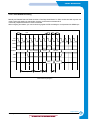
If abnormal image prints periodically, check the parts shown below.
NO
Roller
Abnormal image period
Kind of abnormal image
1
OPC Drum
94.3 mm
White spot. Black spot
2
Charge Roller
37.7 mm
White spot. Black spot
3
Supply Roller
35.8 mm
Horizontal dark band
4
Develope Roller
44.8 mm
Horizontal dark band
5
Transfer Roller
57.8 mm
Black side contamination/transfer fault
6
Heat Roller
82.5 mm
Black spot, White spot
7
Pressure Roller
69.1 mm
Black side contamination
4-20
Samsung Electronics
Troubleshooting
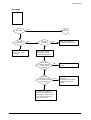
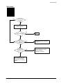
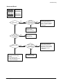
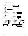
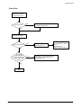
No Image
Digital Printer
Digital Printer
Digital Printer
Digital Printer
Digital Printer
No image?
A on
next page
NO
YES
Self test
pattern prints?
YES
Check connection to
computer or replace
controller
NO
Self testing
is possible ?
NO
Retest after replacing the
connector or controller board
YES
Take out the cartridge
and prepare the tester
for electronic connection
Is the OPC
terminal of machine
is well-connected
to Frame?
NO
Repair or replace the GND
terminal
YES
Does the
video data line to
LSU transit to High/Low
when printing?
NO
Check the path between
Main board
and HVPS. Repair or replace
the defective component
or board
YES
The mirror in LSU might be
misplaced so the light path to the
OPC deviates ->Repair or replace
LSU or remove any defective
matters in the machine
Samsung Electronics
4-21
Troubleshooting
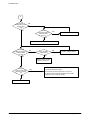
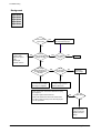
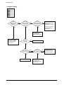
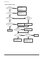
A
Transfer
voltage OK? (on the
transfer roller
shaft)
NO
YES
Are the
connection terminal
and connection
correct?
NO
Repair or replace terminal
YES
Replace HVPS or repair defective component
Developing
(-300V) and supplying
(-450V) voltage
are OK?
NO
Is the connection
terminal OK?
NO
Repair or replace terminal
YES
YES
Replace HVPS or repair
defective component
Does the
counter indicate over
the toner's guaranty
life
YES
NO
Transfer roller might be out of its location
-> Locate the roller into its place
This could occurs when he power of LSU is low or
the density is low due to the obstacles on the window
-> Replace LSU or clean the window
Replace the toner cartridge
4-22
Samsung Electronics
Troubleshooting
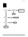
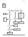
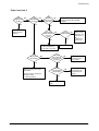
All Black
Digital Printer
Digital Printer
Digital Printer
Digital Printer
Digital Printer
All black in
printing area?
NO
YES
Does the
video data line to LSU
transit to High/Low when
printing?
NO
YES
Check the path among video
controller, engine board,
HVPS, LSU for the shortage
or open -> Repair or replace
the boards
Replace LSU
Is charge
voltage supplied
from HVPS?
NO
Repair or replace HVPS
YES
Is the
Hsync/ signal received
in LSU?
NO
Replace LSU
YES
Charge part's contact
is bad -> Repair or
replace toner cartridge
Samsung Electronics
4-23
Troubleshooting
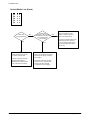
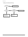
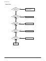
Vertical White Line (Band)
Digital Printer
Digital Printer
Digital Printer
Digital Printer
Digital Printer
White line
missing definitely?
YES
Dirt of dust stuck onto the
window of internal lens of LSU
-> Clean it or replace LSU
Preventive obstacles through
the path between OPC of
developer and LSU prevent the
path -> Remove the obstacles
4-24
NO
Check if the
printout is still has the
same problem even right after
passed through the
transfer roller
NO
YES
The ribs in fuser or toner on the
roller may invoke the image
problem -> Replace the fuser
cover or the defective part
The image is originally black or the
black part is far close to the top
-> Use the pattern which has the
image below bigger than 10mm
from the top
Toner material might be stuck to
blade in the developer inside and it
prevents toner supply -> Replace
the developer
Check both if the toner cartridge's
counter is over its guaranty and
amount of the toner material
-> Replace the toner cartridge
Samsung Electronics
Troubleshooting
Dark Image
Digital Printer
Digital Printer
Digital Printer
Digital Printer
Digital Printer
NO
Dark selected
via RCP?
YES
Change to
Normal and test
Same at Normal?
NO
END
YES
Works cor
with -300V of Bias
voltage?
NO
Repair or replace the defective
component
YES
Works
correctly after
replaced LSU?
NO
Toner over supply due to the
adjustment fault of metering
blade in developer
-> Replace developer
YES
The power of LSU is set
high or internal problem
-> Replace LSU or adjust
volume
Samsung Electronics
4-25
Troubleshooting
Background
Digital Printer
Digital Printer
Digital Printer
Digital Printer
Digital Printer
Recommended
paper used?
NO
Print 20 to 30 pages using
the recommended paper
YES
- Adjust voltage or
replace HVPS
- Repair or replace
after
checking the
terminals' contacts
NO
Transfer,
charge and developing
voltage are OK?
YES
Same problem
occurs?
NO
END
NO
Replace the
toner cartridge
YES
Operating/
storage atmosphere is
too high temperature
/humidity?
YES
Solve the problem under
the recommended condition
(10-32 degree Centigrade)
NO
Dirt or
dust around the
charge roller?
YES
Clean the charge roller
or replace step-up device
/terminal after check
Check Terminals or contacts and 'Guide-Deve Spring'
are misplaced
-> Repair or replace transfer roller etc.
Check if the LED of PTL in front of the transfer roller
is on when it presses the top cover switch on purpose
-> If not, replace PTL
NO
Work OK?
YES
Internal blade or
supplying part of the
developer is defective
-> Replace the toner
cartridge
4-26
Samsung Electronics
Troubleshooting
Ghost
Digital
Digital Printer
Printer
Digital
Digital Printer
Printer
Digital
Digital Printer
Printer
Is it regular
interval of 95mm?
NO
YES
Replace PTL
assembly
NO
Is it regular
interval of 45mm?
Is it regular
interval of 58mm?
(as transfer roller
interval)
NO
YES
YES
A specific part of the transfer
roller has ruined or its
resistance value is changed
-> Replace transfer roller
PTL lamp
works OK?
YES
Check HVPS
contacts and
HVPS's selfoutput
-> If failed,
repair/replace
HVPS
NO
Transfer roller cannot force
regularly due to the gears
eccentricity of transfer roller
-> Replace the defective
component
Developing
/supplying voltage
normal? (-300V/
-500V)
Transfer
voltage is set to
standard?
YES
YES
Irregularity of NIP
between rollers in
developer
-> Replace developer
Bias voltage
is OK? (-300V)
NO
NO
- Repair or replace HVPS
- Check and Repair or
replace the terminal
contacts
Adjust the Bias
voltage or replace
HVPS
YES
Operating/storage
temperature is too low or
not recommended
paper used?
NO
There may be a problem in toner
layer control in toner cartridge
-> Replace the developer
YES
Use the machine with
recommended paper and
at condition
Samsung Electronics
4-27
Troubleshooting
Black Spot
Digital Printer
Digital Printer
Digital Printer
Digital Printer
Digital Printer
Is it regular
interval of 38mm?
NO
YES
The problem occured
since the obstacles
stuck to charge roller
-> Clean the Charge Roller
and then reprint.
4-28
When taking
out the cartridge,
toner leaks?
YES
Toner leaks and much
toner material dropped
onto the paper ->
Replace the developer
NO
Bad image
removes by
scratching?
YES
NO
The problem
randomly occurred
due to the toner
fallen -> Clean the
machine
Check toner is stuck onto
the P/R or H/R in fuser
-> Clean it or replace
Samsung Electronics
Troubleshooting
Horizontal Band
Digital Printer
Digital Printer
Digital Printer
Digital Printer
Digital Printer
Digital Printer
Digital Printer
Digital Printer
Digital Printer
Digital Printer
Black band?
NO
Black band
is far about 95mm from
white band?
NO
YES
The OPC is damaged under the
direct sunlight for around 5
minutes -> If the same problem
persists in 10 hours, replace
the developer
Problem of internal
contacts in OPC
-> Replace developer
The black
band has regular
interval?
NO
This occurs when no
Hsync/ at LSU
-> Replace LSU
YES
94mm interval?
NO
YES
The OPC is damaged due to
the irregular transfer voltage
of HVPS
-> Repair/replace HVPS
-> If the same problem persists,
replace the developer
Samsung Electronics
Does it appear
at every 83mm at
specific place?
YES
NO
Problems of terminal contact,
transfer voltage supplying,
and transfer roller's due to the
charge roller is ruined (38mm)
-> Repair/replace HVPS,
developer
Heat roller is ruined
-> Replace the roller
4-29
Troubleshooting
Irregular Density
OK after
taking out and
rocking the toner
cartridge?
YES
NO
When gray
pattern printing,
irregular density
persists?
NO
YES
transfer/
charge/developing
voltage drops while
printing?
NO
YES
Defective agitator in
the toner supplying part
of developer
->Replace the developer
Check if the 'guide deve
spring' works OK and
repair/repalce
Check high voltage
output and repair/
replace terminals, HVPS
It is over the guaranty
life of toner cartridge
(Check the counter
and replace it)
PTL lamp
works OK?
NO
Replace lamp
YES
Any obstacles
on the PTL lamp?
YES
Clean the window of PTL
4-30
NO
Bad images
NO
around the no image
area?
Irregularity of toner
supply from developer
-> Replace developer
YES
Light distortion due to
the mirror ruined or
LSU's diffused reflection
-> Replace LSU
Samsung Electronics
Troubleshooting
White Spot
Digital Printer
Digital Printer
Digital Printer
Digital Printer
Digital Printer
Is it regular
interval of 95mm?
YES
Obstacles stuck on OPC's
surface
-> Clean the OPC and
machine or replace
developer
NO
Transfer
voltage is normal?
NO
Too high voltage supplied
due to the setting error of
transfer voltage
-> Adjust/replace HVPS
YES
D/R in developing unit has
the defect
-> Replace the developer
When putting in/out the
developer, scratch is made
-> Replace the developer
Samsung Electronics
4-31
Troubleshooting
Trembling at the End When OHP Printing
Recommended
OHP film used?
NO
Use the recommended film
YES
Inserted over
than 10 films into
the MPF?
YES
When multi-page OHP printng,
less than 10 films are
guranteed. (Reduce the
number of films and re-insert
after paper check LED if off)
4-32
NO
When OHP
printing, does the fan
temporarily stops
and revolves?
NO
Use the recommended film
YES
Other parts are touching the
fan and prevents it from
revolution
-> Check and repair
Samsung Electronics
Troubleshooting
Poor Fusing Grade
After printing
NO
completed, any error
related fuser?
YES
Both ends
of thermostat
open?
The machine
placed under the
severe low tempera
ture for a long
time?
YES
NO
NO
While printing,
the voltage of pin 60
of U36 (CPU) on Main
PBA is 2.1V
- 2.6V?
NO
Thermistor's
contact is OK?
NO
YES
YES
Re-assemble
thermistor
Place the machine
at normal
temperature and
re-test
YES
Replace thermostat
and re-test
Open the top
cover. When black
printing, is the fuser NIP
width is 3.03.5mm?
NO
Check if the hardness of
P/R, and spring force is OK?
(hardness: 24 degree,
spring's force: 3 Kg)
YES
Replace the control
component on Main
PBA
Check any contact
problem in thermistor
and repair
Samsung Electronics
The paper used is too
thick or contains too
much cotton in it
-> Re-test with the
recommended paper
4-33
Troubleshooting
4-6-4 Malfunction
Error Status
No power
Check
1. Check power is supplying
2. Check fuse F1 open
Fuser Error
1. Thermostat open
Solution
1. If supplying power differs from machine’s power rating, replace the machine.
2. Replace it.
2. AC wire open
3. Thermistor wire open
4. Main PBA
1. Detach AC connector and measure the resistane
between pin 1 and 2. If it is megohm, thermostat is
open, Replace it.
2. Check bad connector contact or wire is cut.
3. Check thermistor wire and its connection.
4. Replace Main PBA
Cover open
1. When close Side cover, check the lever is
pressed
2. Micro switch’s contact
3. CPU and related circuit
1. Open Side cover and press the lever with pen. If
Controller detects cover close, there is some mechanical trouble in Side cover and lever’s assembly. If not
so there is electrical problem.
Jam 0
Check where Jam 0 happens
1. Paper is not picked up
2. Paper is located in feed sensor
3. Happened when inserting specific papers such
as envelope into the MPF (Multipurpose Paper
Feeder)?
4. Happened when inserting specific papers such
as envelope into the Manual Feeder?
5. Is the Stacker Extender is folded out?
6. Does not the Guide Adjust distort the papers
Jam 1
Paper is stopped in just after of fuser unit.
Jam 2
Check where Jam 2 happens
1. Paper is curled and cannot exit.
2. Paper is curled in the exit cover?.
4-34
1. Check whether solenoid is working or not by using
Engine test mode
2. Check feed sensor malfunction.
3. Re-try inserting a fewer papers.
•fan the papers and align
•take out the loaded papers and insert
them reverse direction
4. Take out the loaded papers and insert them reverse
direction
•inserted papers as recommended for
Manual Feeding?
•When loading, tap the papers until paper detect
sensor senses loading
5. When using long papers, use the Stacker Extender
6. Adjust Guide to fit the paper width
1. It is mostly resulted from double feeding. Check
paper is well stocked in feeder.
2. Check feed actuator position and actuator’s operating. There may be stiff movind or double reflection. If
not so, check the operation of feed sensor by Engine
test mode.
3. Check exit lever operation. Remore jam and check
actuator moving by hand. If actuator is too stiff, paper
is wrapped around the heat roller. Remove obstacles
or replace.
1. Remove paper using pinset or some tool and watch if
separate claws have any troble. Clean around fuser.
2. Check locking works wells. Watch whether the ribs of
exit cover hace any burr or resisitive edge. If they do,
remove obstacles or replace.
Samsung Electronics
Troubleshooting
Error Status
Check
Solution
Jam 2 at
face-down
tray
1. Then paper is not drawn in because of the
stack of papers in the Out tray.
2. Does it curl while coming out?
1. Load recommended quantity of papers
Clutch error
1. Check the spring of solenoid
2. Check the armature assembly/cushion
1. Check whether the spring is expanded or not.
2. Check armature is well installed. It may be unstable
assemble.
3. Remove the Main PBA.
3. Electrical check
High voltage error
1. Check the terminal output voltage
2. Check HVPS
Feeding
obstacles
Does the Plate-knockup prevent the paper
loading?
2. Open the Cover Front and check whether roller or
spring, which are related to paper out, is not out of position. If so, re-locate or replace.
1. Remove the Toner cartridge and open the cover and
press cover open switch lever and measure the voltage
with high voltage probe and sending printing data. If the
voltage is normal, change the toner cartridge.
2. Disassemble the left side cover, and check HV of the solder side of HVPS and change it.
MPF :
Turn the power off and on. Open and close the Side cover
to return to the original state.
Cassette :
Adjust Guide to fit the paper width.
Skew
Is the Guide adjust set to the paper
width?
Fit the paper width using the Guide adjust.
Stacking
1. Took out the Stacker extender to support long
papers?
2. Stacked too many papers more than Stacker
can hold?
1. Use extender as per the paper length.
2. The Face-up stacker normally can hold 100 pages when
using 75g/m2, however, stacking capacity can be lowered
depending on the type of papers.
Engine
Error
Check CBF Harness_CN7.
(Main PBA to LSU)
Refer to troubleshooring “ENGINE ERROR”.
Document
Jam
Document is not picked up(in ADF).
1. Check document is well stocked in ADF.
2. Check whether document was been fastened together
by staple or clip.
3. Load recommended quantity of papers.
Document is stopped after it has fed into the
ADF.
1. Check whether the Reg. sensor is working or not.
2. Check whether the Feed Roller is working or not.
Does it curl while coming out?
1. Check the Open Cover whether there are bosses.
2. Check the ADF ass'y is well assemble.
Samsung Electronics
4-35
Troubleshooting
No Power (LCD NO display LED Off)
Plug in the
power cord?
NO
Check the voltage first and plug
the power cord
YES
The power
NO
voltage supplying is
the same as
rating?
Supply the power as the rating
YES
The fan
revolves when
powered on?
Connections
NO
on board are OK?
NO
YES
YES
LEDs blink
once when
powered on?
NO
Fuse of SMPS
if open?
YES
Repair/replace the
board
4-36
NO
Replace the fuse
YES
YES
Shortage on
the OPE panel
board?
Re-connect firmly
and re-test
NO
The connection
error between
controller board
and panel board
or malfunction
of boards.
-> Replace the
boards
Shortage
between 5V and
GND, or between
24V and
GND?
YES
Remove the shortage
or replace the board
NO
Toner cartridge
is in the set?
NO
Put in the
cartridge
YES
Detect failure due to the
board which detects side
cover open or switch error
-> Replace the board or switch
Samsung Electronics
Troubleshooting
Fuser Error
Measure the resistance
at the both ends of AC
Line with covers open
Less than 10W?
NO
Thermostat is open due to the heat etc.
-> Replace the thermostat
YES
Remove the covers
AC is being supplied?
NO
Re-assemble the top
cover and close it
The voltage of pin #6 of U5
on the Main PBA is about
3.2V?
If not check the
CN4 on the power board.
YES
The voltage
of pin #60 of U36
(CPU) on the Main PBA
is about 2.65V when
printing?
NO
Thermistor, connecting point or engine
board defect -> Repair/replace the
component/board
YES
END
Samsung Electronics
4-37
Troubleshooting
Paper Jam (Mis-Feeding)
Sounds the
solenoid on when starts
print?
NO
The solenoid defected
-> Replace it
YES
Does the
paper move?
The Main PBA board defected
-> Replace boards
NO
The pick-up unit is
assembled wrong
-> Re-assemble or replace
the unit
YES
Does the
paper move more than NO
100mm?
Too many
papers in the
feeder?
YES
Feeder
sensor is assembled
reverse?
YES
NO
The sensor and
Main PBA defected
-> Repair/replace
Reduce the amount
and re-test
YES
Switch them
Paper guides
fit the paper width?
NO
Take out the paper
and re-insert
YES
Paper end curled?
YES
Use the recommended
and quality paper
4-38
NO
Does the
extender pulled out?
NO
Pull out the
extender
YES
<Recommendation>
Use the MPF for the thick
paper such as envelope
and cardstock
Samsung Electronics
Troubleshooting
Paper Jam(Jam 1)
Paper
NO
stopped before
the OPC?
Paper
NO
stopped before
the fuser?
YES
YES
The
actuator of
NO
paper exit sensor
works OK?
Check the actuator exists and its
operation and around the Main PBA
-> Replace
YES
Check the LSU and
if it has the defect
replace it
Is the paper
rolled around the
presseure
roller?
Feeds
NO
multiple pages?
NO
YES
YES
Remove the fuser, remove
the paper and replace the
pressure roller, if necessary
Severe skew
when feeding?
NO
YES
Adjust the paper guides to fit the
paper width
The force of springs pressing the
developer is weak
-> Check guide-DEVE
Check the roller
and ribs of fuser
are in place, and
remove burrs, if
any
-> Remove the
factors of jam
Remove any factors
The paper
came out through
between fuser and
developer?
NO
Check the input path
to the fuser (such as
mis-assembly)
YES
Too thin
or sensitive paper to
static electricity?
NO
Check guide transfer
is grounded Check
the shutter prevents
feeding
YES
Use the recommended
paper
Samsung Electronics
4-39
Troubleshooting
Engine Error
Check
CBF Harness-CN7
(Main B'D to
LSU)
NO
Try again to connector or
Replace connector
YES
Check
Main B'D CN7-9,
P_MOTOR Signal
(
)
NO
Replace Main PBA
YES
Check
Main B'D CN7-8,
LREADY Signal
(
)
NO
Replace LSU
YES
Check
Main B'D CN7-4,
LDON Signal
(
)
NO
Replace Main PBA
YES
Check
Main B'D CN7-1,
HSYNC Signal
(
)
NO
Replace LSU
YES
END
4-40
Samsung Electronics
Troubleshooting
4-6-5 Toner Cartridge and Drum Cartridge Service
It is not guaranteed for the default caused by using other toner and Drum Cartridge cartridge other than the
cartridge supplied by the Samsung Electronic or caused by non-licensed refill production.
Precautions on Safe-keeping of the Drum Cartridge
Excessive exposure to direct light more than a few minutes may cause damage to the cartridge.
Service for the Life of Toner Cartridge
If the printed image is light due to the life of the toner, you can temporarily improve the print quality by redistributing the toner(Shake the toner cartridge), however, you should replace the toner cartridge to solve the
problem thoroughly.
Service for Judgement of Inferior Expendables and the Standard of Guarantee
Please refer to User's Manual or Instructions on Fax/Printer Expendables SVC for the judgement of inferior
expendables and the standard of guarantee besides this service manual.
Samsung Electronics
4-41
Troubleshooting
4-6-5-1 Signs and Measures at Poor toner cartridge
Fault
Light image and
partially blank
image
(The life is ended.)
Digital Printer
Digital Printer
Digital Printer
Digital Printer
Digital Printer
Toner Contamination
Signs
• The printed image is
light or unclean and
untidy.
• Some part of the
image is not
printed.
• Periodically a noise
as "tick tick" occurs.
• Toner is fallen on the
papers periodically.
• Contaminated with
toner on prints
partly or over the
whole surface.
4-42
Cause & Check
Solution
1. If the image is light or unclean
and untidy printed image - Shake
the developer and then recheck.
(1)NG: Check the weight of the
developer
(2)OK: Lack of toner, so the life is
nearly closed.
1. All of 1, 2, 3 aboveIf it become better by shaking, replace
with a new developer after 50-100
sheets in the closing state of the life
span.
2. Some part of image is not printed
- Shake the developer and then
recheck.
(1)NG: Check the weight of the
developer and clean the
LSU window with a cotton
swab, then recheck.
(2)OK: Lack of toner, so the life is
nearly closed.
2. In case of 2If it becomes better after cleaning the
LSU window, then the developer is normal.
(Because of foreign substance on the
LSU window, the image has not been
printed partly.)
3. Periodically a noise as "tick tick"
occurs - Measure the cycle and
the weight of the developer.
3. In case of 3If the cycle of noise is about 2 seconds,
the toner inside the developer has been
nearly exhausted.( Purchase and replace
with a new developer after using about
200 sheets at the point of occurrence)
4. White vertical stripes on the
whole screen or partly :
Check the weight of the developer.
4. In case of 3This is a phenomenon caused by lack of
toner, so replace with a new developer.
1. Toner is fallen on the paper periodically.
(1)Check the cycle of the falling of
the toner.
(2)Check the appearance of both
ends of the developer OPC
drum.
1. If both ends of the OPC drum are contaminated with toner:
Check the life of the developer.
2.The center of the printed matter is
contaminated with toner.
(1)Check whether foreign substances or toner are stuck to the
terminal (contact point) of the
developer.
(2)Check whether the state of the
terminal assembly is normal.
2. Check whether it could be recycled.
Samsung Electronics
Troubleshooting
Fault
White Black spot
Digital Printer
Digital Printer
Digital Printer
Digital Printer
Digital Printer
Signs
• Light or dark black
dots on the image
occur periodically.
• White spots occur in
the image periodically.
Cause & Check
1. If light or dark periodical black
dots occur, this is because the
developer rollers are contaminated with foreign substance or
paper particles.
(1)37.7mm interval :
Charged roller
(2)94.3mm interval :
OPC cycle
1. In case of 1 above Run OPC Cleaning Mode Print 4-5 times
repeatedly to remove. Especially check
foreign substance on the OPC surface,
then remove them with a clean gauze
moistened with IPA(Isopropyl Alcohol) not
to damage OPC if necessary.
2. If white spots occur in a black
image at intervals of 94, 29mm, or
black spots occur elsewhere, the
OPC drum is damaged or foreign
substance is stuck to the surface.
2. In case of 2
If they are not disappeared by running
OPC Cleaning Mode Print 4-5 times.
: at intervals of 94.3mm Replace the developer.
: at intervals of 37.7mm Remove foreign substance, Clean the
Charged Roller
: Broken image Replace the developer according to
carelessness.
3. If a black and white or graphic
image is partially broken at irregular intervals, the transfer roller's
life has been expired or the transfer voltage is abnormal.
Recycled product
• Poor appearance of
the developer.
• Unclean and rough
printouts.
• Bad background in
the image.
Samsung Electronics
Solution
Caution : Never use usual alcohol.
3. In case of 3 - Exchange the transfer
roller because the life of the transfer roller
in use has been expired. (Check the
transfer voltage and readjust if different.)
1. Poor appearance of the developer.
(1)Check the damage to label and
whether different materials are
used.
(2)Check the appearance of parts
of the developer, such as frame,
hopper.
1. In case of 1 (1)If there is an evidence of disassembling
the developer.
(2)If materials other than normal parts of
the developer are added or substituted.
2. Unclean and rough printouts.
(1)Check whether foreign substance or toner are stuck to the
terminal (contact point) of the
developer.
(2)Check whether the state of the
terminal assembly is normal.
2. In case of 2 - If there are any abnormals
in connection with the situation of 1.
(1)It occurs when the developer is recycled over 2 times.
(2)If toner nearly being expired are collected to use, it is judged as the recycled
developer.
4-43
Troubleshooting
Fault
Ghost & Image
Contamination
Signs
• The printed image is
too light or dark, or
partially contaminated black.
• Totally contaminatedblack.
(Black image
printed out)
4-44
Cause & Check
Solution
1. The printed image is too light or
dark, or partially contaminated
black.
(1)Check whether foreign sub
stance or toner are stuck to the
terminal(point of contact) of
the developer.
(2)Check whether the terminal
assembly is normal.
1. All of 1, 2, 3 above
(1)Remove toner and foreign substances
adhered to the contact point of the
developer.
(2)The contact point of the unit facing that
of the developer also must be cleaned.
(3)If the terminal assembly is unsafe:
• Fully stick the terminal to or reassemble
it after disassembling.
• Disassemble the side plate and push
the terminal to be stuck, then reassemble it.
2. Totally contaminated black.
(Black image printed out)
(1)Check whether foreign sub
stances are stuck to the terminal(point of contact) of the
developer and the state of
assembly.
(Especially check the charged
roller terminal.)
2. In case of 2
It is a phenomenon when the OPC drum
of the developer is not electrically
charged. Clean the terminals of the
charged roller, then recheck it.
Samsung Electronics
Troubleshooting
4-6-6 The cause and solutions of bad environment of the software
4-6-6-1 The printer is not working (1)
• Description : While Power turned on, the printer is not working in the printing mode.
Check and Cause
Solution
1. Check if the PC and the printer is properly connected and
the toner cartridge installed.
1. Replace the printer cable. If the problems not solved even
after the cable replaced, check the amount of the remaining
tone.
2. Printing is nor working in the Windows.
2. Check if the connection between PC and printer port is
proper. If you use windows, check if the printer driver in the
controller is set up. If the printer driver is properly set up,
check in which program the printing is not working. The best
way to find out is to open the memo pad to check the function of printing. If it is not working in a certain program, adjust
the setup the program requires. Sometimes, the printout is
normal within the Windows basic programs, but it's not working in a particular program. In such case, install the new
driver again. If not working in the Windows basic program,
Check the setup of the port of CMOS is on ECP. And check
the address of IRQ 7 and 378
3. Check if the printer cable is directly connected to peripheral
devices
3. If the scanner needs to be connected to the printer, first the
remove the scanner from the PC to see if the printer is properly working alone.
4-6-6-2 The printer is not working (2)
• Description : After receiving the printing order, no response at all or the low speed of printing occurs
due to wrong setup of the environment rather than malfunction of the printer itself.
Check and Cause
Solution
1. Secure more space of the hard disk.
1. Not working with the message 'insufficient printer memory'
means hard disk space problem rather than the RAM problem. In this case, provide more space for the hard disk.
Secure more space using the disk utilities program.
2. Printing error occurs even if there is enough space in the
hard disk.
2. The connection of the cable and printer port is not proper.
Check if the connection is properly done and if the parallel
port in CMOS is rightly set up.
3. Check the parallel-port-related items in the CMOS Setup.
3. As a printer port, Select ECP or SPP among SPP(Normal),
ECP, and EPP modes(increase printing speed) SPP normal
mode support 8-bit data transfer, while ECP Mode transfer
the 12-bit data.
4. Reboot the system to print.
4. If the regular font is not printing, the cable or the printer
driver may be defective.
Turn the PC and printer off, and reboot the system to print
again. If not solved, double-click the printer in my computer
If the regular fonts are not printed this time again. the cable
must be defective so replace the cable with new one.
Samsung Electronics
4-45
Troubleshooting
4-6-6-3 Abnormal Printing
• Description : The printing is not working properly even when the cable has no problem.
(even after the cable is replaced) If the printer won't work at all or the strange fonts are
repeated, the printer driver may be defective or wrong setup in the CMOS Setup.
Check and Cause
Solution
1. Set up the parallel port in the CMOS SETUP.
1. Select SPP(Normal) or ECP LPT Port the among ECP,
EPP or SPP in the CMOS Setup.
2. Printer Driver Error.
2. Check the printer in My Computer.(to see if the printer driver
is compatible to the present driver or delete the old driver, if
defective and reinstall the new driver)
3. Error message from insufficient memory.
(The printing job sometimes stops or due to insufficient virtual memory, but it actually comes from the insufficient space
of the hard disk.)
3. Delete the unnecessary files to secure enough space of the
hard disk and start printing job again.
4-6-6-4 SPOOL Error
• Description : To spool which stands for "simultaneous peripheral operations online" a computer document or task list (or "job") is to read it in and store it, usually on a hard disk or larger
storage medium so that it can be printed or otherwise processed at a more convenient
time (for example, when a printer is finished printing its current document).
Check and Cause
Solution
1. Insufficient space of the hard disk in the directory assigned
for the basic spool.
1. Delete the unnecessary files to provide more space to start
printing job.
2. If the previous printing error not solved.
2. If there are some files with the extension name of ****.jnl,
Delete them and Reboot the Windows to restart printing job.
3. When expected to collide with other program.
3. Shut down all other programs except the current one, if possible.
4. When an application program or the printer driver is damaged.
4. Delete the printer driver completely and reinstall it.
5. When some files related to OS are damaged or virus
infected.
5 After rebooting the computer, check for viruses, restore the
damaged files and reinstall the program to do the printing
job.
6. Memory is less than suggested one.
6. Add up enough memory to the PC.
How to delete the data in the spool manager.
In the spool manager, the installed drivers and the list of the documents waiting to be printed are shown.
Select the document to be deleted and check the delete menu.
If you intend to delete the current document being printed, the data being transferred to the printer will be put
out and then the document is removed. Before choosing the document, the menu is still inactive.
Or put the document out of the list and repeat the routine as in the above or finish the spool manager.
4-46
Samsung Electronics
Exploded Views and Parts List
Appendix information
The following list shows different materials by model.
The material codes mentioned in themanual are subject to change without prior notice.
For the latest exact information, see ITSELF SYSTEM. (http://itself.sec.samsung.co.kr)
•SCX-5312F/XAA
•SCX-5112/XAA
DESCRIPTION
SEC.CODE
AS-SCANNER ASS’Y(FRU)
AS-PLATEN ASS’Y(FRU)
AS-OPE COVER ASS’Y(FRU)
PMO-COVER OPE(C)
PCT-ONETOUCH PAPER
PCT-LCD WINDOW
PMO-COVER DUMMY OPE(M)
PBA SUB-LIU
JC81-00691A
JC81-00690A
JC81-00689A
JC72-00796A
JC72-00872A
JC72-00870A
JC72-00858A
JC92-01355A
•SCX-5312F/XEU
AS-SCANNER ASS’Y(FRU)
SEC.CODE
JC81-00742A
AS-PLATEN ASS’Y(FRU)
JC81-00745A
AS-OPE COVER ASS’Y(FRU)
JC81-00748A
PMO-COVER OPE(C)
JC72-00944A
PCT-LCD WINDOW
JC72-00945A
•SCX-5112/XEU
DESCRIPTION
SEC.CODE
AS-SCANNER ASS’Y(FRU)
AS-PLATEN ASS’Y(FRU)
AS-OPE COVER ASS’Y(FRU)
PMO-COVER OPE(C)
PCT-ONETOUCH PAPER
PCT-LCD WINDOW
PMO-COVER DUMMY OPE(M)
PBA SUB-LIU
JC81-00691A
JC81-00690A
JC81-00689A
JC72-00796A
JC72-00872A
JC72-00870A
JC72-00858A
JC92-01355G
•SCX-5312F/XEG
DESCRIPTION
SEC.CODE
AS-SCANNER ASS’Y(FRU)
JC81-00742A
AS-PLATEN ASS’Y(FRU)
JC81-00745A
AS-OPE COVER ASS’Y(FRU)
JC81-00748A
PMO-COVER OPE(C)
JC72-00944A
PCT-LCD WINDOW
JC72-00945A
•SCX-5112/XEG
DESCRIPTION
SEC.CODE
AS-SCANNER ASS’Y(FRU)
AS-PLATEN ASS’Y(FRU)
AS-OPE COVER ASS’Y(FRU)
PMO-COVER OPE(C)
PCT-ONETOUCH PAPER
PCT-LCD WINDOW
PMO-COVER DUMMY OPE(M)
PBA SUB-LIU
JC81-00691B
JC81-00690F
JC81-00689F
JC72-00796C
JC72-00872C
JC72-00870C
JC72-00858C
JC92-01355E
DESCRIPTION
SEC.CODE
AS-SCANNER ASS’Y(FRU)
JC81-00742B
AS-PLATEN ASS’Y(FRU)
JC81-00745B
AS-OPE COVER ASS’Y(FRU)
JC81-00748B
PMO-COVER OPE(C)
JC72-00944C
PCT-LCD WINDOW
JC72-00945C
•SCX-5112/XEF
•SCX-5312F/XEF
DESCRIPTION
SEC.CODE
AS-SCANNER ASS’Y(FRU)
AS-PLATEN ASS’Y(FRU)
AS-OPE COVER ASS’Y(FRU)
PMO-COVER OPE(C)
PCT-ONETOUCH PAPER
PCT-LCD WINDOW
PMO-COVER DUMMY OPE(M)
PBA SUB-LIU
JC81-00691C
JC81-00690E
JC81-00689E
JC72-00796D
JC72-00872D
JC72-00870D
JC72-00858D
JC92-01355E
Samsung Electronics
DESCRIPTION
DESCRIPTION
SEC.CODE
AS-SCANNER ASS’Y(FRU)
JC81-00742C
AS-PLATEN ASS’Y(FRU)
JC81-00745C
AS-OPE COVER ASS’Y(FRU)
JC81-00748C
PMO-COVER OPE(C)
JC72-00944D
PCT-LCD WINDOW
JC72-00945D
i
Exploded Views and Parts List
•SCX-5312F/XEC
•SCX-5112/XEC
DESCRIPTION
SEC.CODE
AS-SCANNER ASS’Y(FRU)
AS-PLATEN ASS’Y(FRU)
AS-OPE COVER ASS’Y(FRU)
PMO-COVER OPE(C)
PCT-ONETOUCH PAPER
PCT-LCD WINDOW
PMO-COVER DUMMY OPE(M)
PBA SUB-LIU
JC81-00691E
JC81-00690C
JC81-00689C
JC72-00796E
JC72-00872E
JC72-00870E
JC72-00858E
JC92-01355E
•SCX-5312F/XET
SEC.CODE
AS-SCANNER ASS’Y(FRU)
JC81-00742E
AS-PLATEN ASS’Y(FRU)
JC81-00745E
AS-OPE COVER ASS’Y(FRU)
JC81-00748E
PMO-COVER OPE(C)
JC72-00944E
PCT-LCD WINDOW
JC72-00945E
•SCX-5112/XET
DESCRIPTION
SEC.CODE
AS-SCANNER ASS’Y(FRU)
AS-PLATEN ASS’Y(FRU)
AS-OPE COVER ASS’Y(FRU)
PMO-COVER OPE(C)
PCT-ONETOUCH PAPER
PCT-LCD WINDOW
PMO-COVER DUMMY OPE(M)
PBA SUB-LIU
JC81-00691D
JC81-00690D
JC81-00689D
JC72-00796F
JC72-00872F
JC72-00870F
JC72-00858F
JC92-01355E
DESCRIPTION
AS-SCANNER ASS’Y(FRU)
SEC.CODE
JC81-00742D
AS-PLATEN ASS’Y(FRU)
JC81-00745D
AS-OPE COVER ASS’Y(FRU)
JC81-00748D
PMO-COVER OPE(C)
JC72-00944F
PCT-LCD WINDOW
JC72-00945F
•SCX-5112/XIL
•SCX-5312F/XIL
DESCRIPTION
DESCRIPTION
SEC.CODE
DESCRIPTION
SEC.CODE
AS-SCANNER ASS’Y(FRU)
JC81-00691F
AS-SCANNER ASS’Y(FRU)
JC81-00742F
AS-PLATEN ASS’Y(FRU)
JC81-00690B
AS-PLATEN ASS’Y(FRU)
JC81-00745F
AS-OPE COVER ASS’Y(FRU)
JC81-00689B
AS-OPE COVER ASS’Y(FRU)
JC81-00748F
PMO-COVER OPE(C)
JC72-00796G
PMO-COVER OPE(C)
JC72-00944G
PCT-ONETOUCH PAPER
JC72-00872G
PCT-LCD WINDOW
JC72-00945G
PCT-LCD WINDOW
JC72-00870G
PMO-COVER DUMMY OPE(M)
JC72-00858G
PBA SUB-LIU
JC92-01355A
•SCX-5312F/XSA
ii
DESCRIPTION
SEC.CODE
AS-SCANNER ASS’Y(FRU)
AS-PLATEN ASS’Y(FRU)
AS-OPE COVER ASS’Y(FRU)
PMO-COVER OPE(C)
PCT-ONETOUCH PAPER
PCT-LCD WINDOW
PMO-COVER DUMMY OPE(M)
PBA SUB-LIU
JC81-00691A
JC81-00690A
JC81-00689A
JC72-00796A
JC72-00872A
JC72-00870A
JC72-00858A
JC92-01355F
Samsung Electronics
Exploded Views and Parts List
5. Exploded View & Parts List
5-1. Main Exploded View & Parts List.......................................
5-2. Platen Ass’y Exploded View & Parts List....................
5-3. ADF ASS’Y Exploded View & Parts List......................
5-4. Side Cover Ass’y Exploded View & Parts List...........
5-5. Cassette Ass’y Exploded View & Parts List...............
5-6. Exit Ass’y Exploded View & Parts List................................
5-7. Feeder Ass’y Exploded View & Parts List..................
5-8. MP Ass’y Exploded View & Parts List.........................
5-9. Base Frame Exploded View & Parts List....................
5-10.Pick-up Ass’y Exploded View & Parts List................
5-11. Drive Ass’y Exploded View & Parts List...........................
5-12. Main Frame Ass’y Exploded View & Parts List.................
5-13. FuserAss’y Exploded View & Parts List...........................
5-14. Screw .....................................................................................
Samsung Electronics
page(5-2)
page(5-5)
page(5-9)
page(5-12)
page(5-14)
page(5-16)
page(5-18)
page(5-20)
page(5-22)
page(5-24)
page(5-26)
page(5-28)
page(5-30)
page(5-32)
5-1
5-2
2-2
2-1
2
1-5
1-6
1-6
1-3
20
1-4
1-2
25
SCX-5112
SCX-5312F
1-1
39
1
3
28
47
34
4
6
5
12
7
46
35
45
26
8
26-1
43
15
9
49
26-3
24
13
44
16
26-2
26-3
48
17
37
21-1
38
50
53
53-2
53-153-3
11
30
37
14
21-2
23
51
33
21
19
10
52
52-4
52-3 52-2
52-1
29
42
41
18
27
18-2
40
36
18-1
Exploded Views and Parts List
5-1. Main Exploded View & Parts List
Samsung Electronics
Exploded Views and Parts List
Main Parts List
( SA. : Service Available )
NO
1
1-1
1-2
1-3
1-4
1-5
1-6
2
2-1
2-2
3
4
5
6
7
8
9
10
11
12
13
14
15
16
17
18
18-1
18-2
19
19
20
21
21-1
21-2
23
24
25
26
26-1
26-2
26-3
DESCRIPTION
SCANNER ASS’Y(FRO)
ELA HOU-ADF ASS’Y
ELA HOU-PLATEN ASS’Y
PMO-COVER OPEN
PMO-COVER SIDE L
PMO-COVER SIDE R
PMO-GUIDE PAPER
MEA UNIT-COVER PA EXIT ASS’Y
PMO-TRAY EXTENTION MP NE
PMO-COVER PAPER EXIT
MEC-CASSETTE ASS’Y(LETTER)
MEA UNIT-COVER FRONT ASS’Y
UNIT-LSU
SMPS-SMPS(V1)+HVPS
SMPS-SMPS(V2)+HVPS
ELA-OPC UNIT SET
ELA-TONER UNIT SET
ELA HOU-PICKUP ASS’Y
ELA HOU-SIDE COVER ASS’Y
ELA HOU-MP ASS’Y
ELA HOU-BASE FRAME ASS’Y
MEC-FEED ASS’Y
ELA HOU-FUSER(110V)ASS’Y
ELA HOU-FUSER(220V)ASS’Y
ELA HOU-FRAME MAIN ASS’Y
MEC-EXIT ASS’Y
ELA HOU-DRIVE ASS’Y
MEA UNIT-COVER REAR ASS’Y
PMO-COVER SIMM,XRX
PMO-COVER REAR
PBA MAIN-MAIN
PBA MAIN-MAIN
PMO-CONNECT PAPER MFP
PMO-CONNECT PAPER MFP
ELA HOU-DUCT FAN
FAN-DC
PMO-DUCT FAN
CBF POWER STITCH GRAY
SOLENOID-PICK UP
PMO-COVER EXIT REAR
MEA UNIT GUIDE CST PA ASS’Y
PMO-SHEET GUIDE PAPER
PMO-GUIDE CASSETTE RAIL
SHEET FEED
SEC CODE
Q’TY
SA
refer to the table
JC81-00429A
refer to the table
JC72-00737A
JC72-00739A
JC72-00740A
JB72-00843A
JC97-01556A
JC72-00354B
JC72-00786A
JC97-01642A
JC97-01572A
JC59-00014A
JC44-00039A
JC44-00035A
*
*
JC96-02180A
JC96-02183A
JC96-02182A
*
JC75-00143A
JC96-02194A
JC96-02178A
JC96-02184A
JC97-01643A
JC96-02181A
JC97-01557A
JC72-41224B
JC72-00788A
JC92-01354A
JC92-01399A
JC72-00782A
JC72-00782B
JC96-02311A
JC31-00012A
JC72-00807A
JC39-00055B
JC33-00007A
JC72-00790A
JC97-01575A
JC72-00836A
JC72-00791A
JC72-00078A
1
1
1
1
1
1
2
1
1
1
1
1
1
1
1
1
1
1
1
1
1
1
1
1
1
1
1
1
1
1
1
1
1
1
1
1
1
1
1
1
1
1
1
2
O
O
O
O
O
O
O
O
O
O
O
O
O
O
O
X
X
O
O
O
X
O
O
O
O
O
O
O
O
O
O
O
O
O
O
O
O
O
O
O
O
O
O
O
REMARK
LETTER/A4
110V
220V
110V
220V
SCX-5312F
SCX-5112
SCX-5312F
SCX-5112
O : Service available X : Service not available
Samsung Electronics
5-3
Exploded Views and Parts List
Main Parts List (Cont.)
( SA. : Service Available )
NO
27
28
29
30
31
32
33
34
35
36
37
38
39
40
41
42
43
44
45
46
47
48
49
50
51
52
52-1
52-2
52-3
52-4
53
53-1
53-2
53-3
DESCRIPTION
PBA SUB-LIU
PMO-DUMMY BASE FRAME
IPR-SHIELD MAIN LOWER
PMO-COVER FEED AY
PMO-COVER BRKT MOTER
PMO-GUIDE PAPER OUT
SHEET-CONNECTOR
CBF HARNESS-LSU
CBF HARNESS-POWER+HVPS
CBF HARNESS-LIU
CBF HARNESS-LIU GND
CBF HARNESS-INLET(KOR)
IPR-SHIELD SMPS UPPER
IPR-SHIELD MAIN UPPER
IPR-SHIELD SIMM
SUPPORTER
PMO-WINDOW SENSOR DEVE
PMO-CAM JAM REMOVE
PMO-LOCKER DEVE
PMO-LEVER JAM REMOVE
IPR-SHIELD SMPS LOWER
GEAR-PICK-UP
PMO-BEARING SHAFT
GEAR-TRANSFER
MEC-ROLLER TRANSFER
MEA UNIT-HOLDER GEAR ASS’Y
SPRING ETC-PLATE TR
SPRING ETC-TR_L
PMO-BUSH
PMO-HOLDER GND TR
MEA UNIT-HOLDER GND ASS’Y
SPRING ETC-TR_R
PMO-BUSH
PMO-HOLDER GEAR TR
SEC CODE
Q’TY
SA
JC92-01355A
JC72-00789A
JC70-00245A
JC72-00801A
JC72-00834A
JC72-00835A
*
*
*
*
*
*
*
*
*
*
*
JC72-00799A
JC72-00805A
JC72-00804A
JC70-00247A
JC66-00335A
JC72-41191A
JC66-40947A
JC75-00148A
JC97-01573A
*
*
*
*
JC97-01574A
*
*
*
1
1
1
1
1
1
1
1
1
1
2
1
1
1
1
2
1
1
1
1
1
1
1
1
1
1
1
1
1
1
1
1
1
1
O
O
O
O
O
O
X
X
X
X
X
X
X
X
X
X
X
O
O
O
O
O
O
O
O
O
X
X
X
X
O
X
X
X
REMARK
ONLY SCX-5312F
ONLY SCX-5312F
ONLY SCX-5312F
O : Service available X : Service not available
5-4
Samsung Electronics
Exploded Views and Parts List
5-2. Platen Ass’y Exploded View & Parts List
1-1-1
1-1-2
S6
1-1
1-1-3
S6
SCX-5112
1-1-4
SCX-5312F
1-2
0
1-3
SCX-5312F
1-4
S5
1-4
1-5-1
S5
1-4
S5
SCX-5112
1-5-2
1-5
2-17
3
2-1
2-2
2-16
2-15
2-14
1
2-6
2-13
2-19
2-5
2-21-1
2-4
2-7-3
2-7-5
2-18
2-20
2-7-3
2-7-4
2-7-6
2-7-2
2-22
2
2-3
2-7-1
2-7-1
2-21
2-7-7
S9
2-8
2-7
S6
2-9
S6
2-11
2-10
2-12
S11
Samsung Electronics
5-5
Exploded Views and Parts List
3-5
3-21
3-15
3-4
3-3
3-3
3-2
3-2
3-6
3-1
3-1
3-7
3-8
3-10
3-4
3-12
3-5
3-13
3-15
3-16
3-9
3-6
3-7
3-12
3-14
3-8
3-11
3-11
3-17 3-18
3-10 3-9
3-19
3-20
S6
3-14
S6
S9
S9
S6
SCX-5312F
5-6
3-13
S6
S6
S6
SCX-5112
Samsung Electronics
Exploded Views and Parts List
Platen Ass’y Parts List
( SA. : Service Available )
NO
0
1
1-1
1-1-1
1-1-2
1-1-3
1-1-4
1-2
1-3
1-4
1-5
1-5-1
1-5-2
2
2-1
2-2
2-3
2-4
2-5
2-6
2-7
2-7-1
2-7-2
2-7-3
2-7-4
2-7-5
2-7-6
2-7-7
2-8
2-9
2-10
2-11
2-12
2-13
2-14
2-15
2-16
2-17
2-18
2-19
2-20
2-21
2-21-1
2-22
DESCRIPTION
ELA HOU-PLATEN ASS’Y
MEA UNIT-SCAN UPPER ASS'Y
AS-DUMMY UPPER AS(FRV)
MCT-GLASS ADF
LABEL(L)-REGISTRATION EDGE (L)
PMO-DUMMY UPPER
SHEET-DUMMY UPPER
PPR-REGISTRATION EDGE (F)
PMO-COVER SCAN UPPER
IPR-HOLDER GLASS
MEA UNIT-GLASS PLATEN ASS'Y
LABEL(P)-SHEET SHADING(B)
MCT-GLASS SCANNER(LEGAL)
ELA HOU-SCAN LOWER ASS'Y(SEC)
BELT-TIMING GEAR
SPRING ETC-BELT
CBF HARNESS-SCAN MOTOR
CBF HARNESS-MAIN-ENGINE
CBF HARNESS-DRIVER GND
PBA SUB-D-SUB
ELA HOU-SCAN MOTOR ASS'Y
MOTOR-SCAN
GEAR-TIMING
RING-E
GEAR-REDUCTION
PMO-HOLDER BELT
GEAR-IDLE
IPR-BRK MOTOR(PLATEN)
CBF HARNESS-OPE
PMO-COVER SCAN LOWER
IPR-CHANNEL BASE FRAME
PMO-HOLDER CCD
PMO-COVER DUMMY LOWER (C)
ICT-INSERT SHAFT
PMO-PULLEY
PMO-HOLDER BELT
RING-E
ICT-SHAFT CCD
PMO-LEVER SENSOR
IPR-BRK SCAN B'D
SPRING ETC-EXIT
ELEC/MECH-SCANNER MODULE
AS-LAMP CCD
CBF SIGNAL-CCD FFC
SEC CODE
Q’TY
SA
refer to the table
JC97-01579A
JC81-00426A
*
*
*
*
JC72-00809A
JC72-00758A
JB70-00148A
JC97-01580A
*
*
*
6602-001090
JB61-00059A
JB39-00077A
JC39-00030A
JB39-00065A
JC81-00781A
JC81-00431A
*
*
*
*
*
*
*
*
JC72-00757A
JC70-00239A
JB72-00759A
JC72-00794A
JB70-00154A
JB72-00763A
JB72-00764A
6044-000125
JC70-00253A
JC72-00755A
JC70-00228A
JB61-70939A
JC96-02105A
JC81-00783A
JC39-00188A
1
1
1
1
1
1
1
1
1
3
1
1
1
1
1
1
1
1
1
1
1
1
1
3
1
1
1
1
1
1
1
1
1
1
1
1
1
1
1
1
1
1
1
1
O
O
O
X
X
X
X
O
O
O
O
X
X
X
O
O
O
O
O
O
O
X
X
X
X
X
X
X
X
O
O
O
O
O
O
O
O
O
O
O
O
O
O
O
REMARK
O : Service available X : Service not available
Samsung Electronics
5-7
Exploded Views and Parts List
SCX-5312F (OPE)
NO
3
DESCRIPTION
ELA HOU-OPE COVER ASS’Y
SEC CODE
Q’TY
SA
refer to the table
1
O
3-1
PMO-COVER OPE(C)
refer to the table
1
O
3-2
PCT-LCD WINDOW
refer to the table
1
O
3-3
PMO-COVER DUMMY OPE(M)
refer to the table
1
O
3-4
PCT-ONETOUCH PAPER
refer to the table
1
O
3-5
PCT-ONETOUCH CARD
JC72-00871A
1
O
3-6
PMO-KEY ONETOUCH
JC72-00860A
1
O
3-7
PMO-KEY SHIFT
JC72-00861A
1
O
3-8
PMO-KEY FAX
JC72-00862A
1
O
3-9
RMO-RUBBER ONETOUCH
JC73-00104A
1
O
3-10
PMO-KEY SCROLL
JC72-00866A
1
O
3-11
RMO-RUBBER SCROLL
JC73-00106A
1
O
3-12
PMO-KEY COPY
JC72-00863A
1
O
3-13
PMO-KEY TEL
JC72-00865A
1
O
3-14
PMO-KEY OHD
JC72-00864A
1
O
3-15
PMO-KEY SAVE(T)
JC72-00923A
1
O
3-16
PMO-KEY SAVE
JC72-00867A
1
O
3-17
PMO-KEY START
JC72-00868A
1
O
3-18
PMO-KEY STOP
JC72-00869A
1
O
3-19
RMO-RUBBER TEL
JC73-00105A
1
O
3-20
PBA SUB-OPE(KOR)
JC92-01380B
1
O
3-21
NPR-BADGE
JC71-00008A
1
O
SEC CODE
Q’TY
SA
refer to the table
1
O
REMARK
SCX-5112 (OPE)
NO
3
DESCRIPTION
ELA HOU-OPE COVER ASS'Y(C)
3-1
PMO-OPE COVER
refer to the table
1
O
3-2
PCT-LCD WINDOW
refer to the table
1
O
3-3
PMO-COVER DUMMY OPE(C)
refer to the table
1
O
3-4
PMO-KEY SCROLL
JC72-00866A
1
O
3-5
PMO-KEY COPY
JC72-00863A
1
O
3-6
PMO-KEY TEL
JC72-00865A
1
O
3-7
PMO-KEY SAVE(T)
JC72-00923A
1
O
3-8
PMO-KEY SAVE
JC72-00867A
1
O
3-9
PMO-KEY STOP
JC72-00869A
1
O
3-10
PMO-KEY START
JC72-00868A
1
O
3-11
PMO-KEY OHD
JC72-00864B
1
O
3-12
RMO-RUBBER SCROLL
JC73-00106A
1
O
3-13
RMO-RUBBER TEL
JC73-00105A
1
O
3-14
PBA SUB-OPE(KOR)
JC92-01380B
1
O
3-15
NPR-BADGE
JC71-00008A
1
O
5-8
REMARK
Samsung Electronics
Exploded Views and Parts List
5-3. ADF ASS’Y Exploded View & Parts List
0
1-1
1-2
1-3
1-5
1-4
5
S11
S5
S11
S11
2
S11
1-6-2
1-6-6
1-6
1-6-1
2-6
S11
2-1
1-6-3
1-6-5
1-6-4
1-12
2-2
1-13
1-4
2-3
S6
2-4
1-10
S6
1-15
2-5
1-7
S6
1-8
1-9
1-11
3-16
S6
4-3
4-4
3-22
4-1
3-1
S10 4-5
4-11
4-6
4-7
S10
1
3-17
3-2
3-3
3-21
3-2
3-7
4-7
4-10
4-9
4-8
S10
4-5
S6
4-2
3-4
3-19
3-8
3-2
3-5
3-18
3-4
3
4
3-6
3-23
S6
S6
3-12
3-11
3-10
3-20
3-9
3-13
3-13
Samsung Electronics
3-14
3-15
5-9
Exploded Views and Parts List
ADF Ass’y Parts List
( SA. : Service Available )
NO
0
1
1-1
1-2
1-3
1-4
1-5
1-6
1-6-1
1-6-2
1-6-3
1-6-4
1-6-5
1-6-6
1-7
1-8
1-9
1-10
1-11
1-12
1-13
1-14
1-15
2
2-1
2-2
2-3
2-4
2-5
2-6
3
3-1
3-2
3-3
3-4
3-5
3-6
3-7
3-8
3-9
3-10
DESCRIPTION
AS-ADF ASS’Y(FRU)
MEC UNIT-PLATEN COVER ASS’Y
PMO-TX STACKER
IPR-WASHER SPRING CU
PMO-DOC GUIDE L
PMO-DOC GUIDE R
PMO-GEAR PINION
MEA UNIT-HINGE ASS’Y
SPRING ETC-HINGE PLATE
PMO-HINGE PLATEN
ICT-BUSHING HINGE
PMO-HSG HINGE
ICT-SHAFT HINGE
RING-C
RPR-ROLLER EXIT IDLE
IPR-SHAFT EXIT
NPR-SPRING PINCH DRIVE
PMO-COVER PLATEN
PPR-SPONG SHEET
PPR-SHEET PLATEN
IPR-SPRING PINCH
ICT-SHAFT PINCH
PMO-ROLL PINCH
MEA UNIT-ADF UPPER ASS’Y
PMO-COVER ADF UPPER
PMO-ADF RUBBER
PMO-HOLDER ADF
RPR-SPONGE ADF
SPRING ETC-COIL ADF
SHEET ADF
AS-ADF LOWER ASS’Y(FRU)
SPRING ETC-TORSION DOC(CC2-F)
RING-C
GEAR-ADF 38
PMO-BUSH
MEC-ROLLER DRIVER
PMO-COVER ADF LOWER
PMO-ACTUATOR SENSOR DOC.
PMO-ACTUATOR SENSOR REGI
MEC-ROLLER EXIT
PMO-BUSHING HOLDER
SEC CODE
Q’TY
SA
JC81-00429A
JC97-01585A
JC72-00745A
JF70-10616A
JC72-00839A
JC72-00838A
JF72-41354A
JC97-01586A
*
*
*
*
*
*
JC73-00091A
JC70-00242A
JB71-00038A
JC72-00738A
JC72-00751A
JC72-00750A
JC70-00260A
JC70-00265A
JG72-40663A
JC97-01581A
*
*
*
*
*
*
JC81-00434A
JB61-00076A
6044-000159
JB66-00103A
JB72-00819A
JC75-00149A
JC72-00735A
JB72-00837A
JC72-00747A
JC75-00150A
JG72-40732A
1
1
1
2
1
1
1
2
1
1
1
1
1
1
2
1
2
1
1
1
3
3
3
1
1
1
1
1
1
1
1
3
4
1
2
1
1
1
1
1
1
O
O
O
O
O
O
O
O
X
X
X
X
X
X
O
O
O
O
O
O
O
O
O
O
X
X
X
X
X
X
O
O
O
O
O
O
O
O
O
O
O
REMARK
O : Service available X : Service not available
5-10
Samsung Electronics
Exploded Views and Parts List
ADF Ass’y Parts List (Cont.)
( SA. : Service Available )
NO
DESCRIPTION
SEC CODE
Q’TY
SA
3-11
SPRING ETC-CLUTCH
JC61-00062A
1
O
3-12
GEAR-EXIT 23
JC66-00323A
1
O
3-13
SPRING ETC-WHITE BAR
JC61-00548A
2
O
3-14
IPR-BRKT WHITE BAR
JC70-00225A
1
O
3-15
PPR-WHITE BAR SHEET
JC72-00752A
1
O
3-16
CBF D SUB CBL-ADF_MAIN
JC39-00190A
1
O
3-17
AS-PBA SUB-ADF(FRU)
JC81-00437A
1
O
3-18
PBA SUB-ADF POSSEN
JC92-01365A
1
O
3-19
PBA SUB-ADF DET SEN
JC92-01366A
1
O
3-20
CBF HARNESS-ADF ROLLER GND
JC39-00187A
1
O
3-21
CBF HARNESS-DRIVER GND
JB39-00065A
1
O
3-22
PMO-ACTUATOR SENSOR SCAN
JC72-00746A
1
O
3-23
NPR-SPRING GND
*
1
X
JC81-00435A
1
O
4
AS-ADF MOTOR AS (FRU)
GEAR CLUTCH 29
*
1
X
4-2
IPR-BRKT ADF MOTOR
*
1
X
4-3
PMO-WHITE CLUTCH SUB 29
*
1
X
4-4
GEAR-CLUTCH 39
*
1
X
4-5
GEAR-IDLE 20/33
*
2
X
4-6
RING-C
*
7
X
4-7
GEAR-IDLE 17/35
*
2
X
4-8
GEAR IDLE 25
*
1
X
4-9
MOTOR ADF
*
1
X
4-10
GEAR-JAM REMOVE
*
1
X
4-11
GEAR REDUCTION45/19
*
1
X
JC97-01582A
1
O
5
4-1
MEC UNIT-PICK UP ASS’Y
REMARK
O : Service available X : Service not available
Samsung Electronics
5-11
Exploded Views and Parts List
5-4. Side Cover Ass’y Exploded View & Parts List
1
S6
5
15
1-4 1-4
S5
11-4
14
13
S6
1-2
1-5
0
11
2
17
4
16
1-8
1-8
1-10
1-11
9
3
1-10
1-6
1-9
1-3
1-9
1-13
S6
1-3
1-7
S6
8
1-1
S6
6
10-2
10-7
10-3
7
12
10-4
10-6
10-5
10-1
10
5-12
Samsung Electronics
Exploded Views and Parts List
Side Cover Ass’y Parts List
( SA. : Service Available )
NO
0
DESCRIPTION
ELA HOU-SIDE COVER ASS’Y
1
MEA UNIT-DUPLEX ASS’Y
SEC CODE
Q’TY
SA
JC96-02183A
1
O
*
1
X
JC72-00806A
1
O
1-1
PMO-GUIDE DP SIDE
1-2
RING-CS
6044-000001
2
O
1-3
SPRING-FUSER EXIT
JC61-70976A
2
O
1-4
GEAR-DUP IDLER 17
JC66-00341A
3
O
1-5
GEAR-MP/DUP DRV
JC66-00346A
1
O
1-6
IPR-BRKT G DUP
JC70-00233A
1
O
1-7
PMO-GP LOWER DP
JC72-00732A
1
O
1-8
PMO-SHAFT DUP DRIVER
JC72-00764A
2
O
1-9
PMO-ROLLER_EXIT
JC72-40361A
2
O
1-10
RPR-RUBBER EXIT
JC73-10203A
2
O
1-11
PMO-BUSHING TX(B4)
JG72-40744A
4
O
1-12
PMO-TIE STOPPER
JC72-00766A
2
O
1-13
CBF HARNESS-SCAN GND
JC39-00046A
1
O
2
IPR-PLATE SAW
JC70-10232A
2
O
3
PMO-FEED FRAME
JC72-00731A
1
O
4
PMO-HOLDER SAW
JC72-41213A
1
O
5
IPR-BRACKET GUIDE A
JC70-00229A
1
O
6
PMO-LOCKER SIDE R
JC72-00763A
1
O
7
PMO-LOCKER OPEN
JC72-00762A
1
O
8
SPRING-LOCKER TORSION
JC61-00479A
1
O
9
SPRING-FEED
JC61-00478A
2
O
10
MEC UNIT-TRAY ASS’Y
JC97-01577A
1
O
10-1
PMO-TRAY CASE, MP
*
1
X
10-2
PMO-TRAY-EXT, MP
*
1
X
10-3
PMO-SIDE GUIDE, MP
*
1
X
10-4
PMO-TRAY COVER, MP
*
1
X
10-5
IPR-GUIDE LATCH, MP
*
1
X
10-6
PMO-TRAY LINK,MP
*
1
X
10-7
LABEL(R)-HEIGHT,MP
*
1
X
11
CBF HARNESS-OPE GND
JC39-00036A
1
O
12
PMO-TIE STOPPER
JC72-00766A
2
O
13
IPR-BRKT GROUND B
JC70-00230A
1
O
14
IPR-BRKT GROUND TR
JC70-00231A
1
O
15
IPR-BRKT GROUND A
JC70-00232A
1
O
16
IPR-BRACKET GUIDE B
JC70-00234A
1
O
17
PMO-BUSHING FEED
JC72-00730A
1
O
REMARK
O : Service available X : Service not available
Samsung Electronics
5-13
Exploded Views and Parts List
5-5. Cassette Ass’y Exploded View & Parts List
0
11
3
13
13
7
S6
8
2
15
14
1
5
4
12
10
6
9
16
5-14
Samsung Electronics
Exploded Views and Parts List
Cassette Ass’y Parts List
( SA. : Service Available )
NO
DESCRIPTION
SEC CODE
Q’TY
SA
0
MEA UNIT-CASSETTE(A4) ASS’Y
JC97-01642A
1
O
1
IPR-FINGE
*
1
X
2
IPR-GUIDE PLT PAPER
*
1
X
3
IPR-PLATE K/UP
JC70-00221A
1
X
4
IPR-SPR PLT G/SIDE
JC70-10929A
1
O
5
PMO-COVER CASSETTE(C)
*
1
X
6
PMO-FRAME CASSETTE
*
1
X
7
PMO-GUIDE FRONT CST
*
1
X
8
PMO-GUIDE REAR
JC72-00717A
1
O
9
PMO-GUIDE/SIDE CST
JC72-40967D
1
O
10
PMO-LOCKER PLATE
JC72-41210A
1
O
11
PRP-PAD CST
JC73-10910A
2
O
12
SPRING-LOCKER PLATE
JG61-70531A
1
O
13
SPRING-PLATE K/UP
JC61-00455A
2
O
14
LABEL(R)-INSTRUCTION CST
*
1
X
15
LABEL(R)-HEIGHT CST
*
1
X
16
PMO-IMPACT CASSETTE
*
1
X
REMARK
O : Service available X : Service not available
Samsung Electronics
5-15
Exploded Views and Parts List
5-6. Exit Ass’y Exploded View & Parts List
9
6
21
7
21
8
10
5
6
21
4
5
4
10
10
19
20
22
11
S6
1
17
15
16
18
3
13
12
14
2
S6
5-16
Samsung Electronics
Exploded Views and Parts List
Exit Ass’y Parts List
( SA. : Service Available )
NO
DESCRIPTION
SEC CODE
Q’TY
SA
JC97-01643A
1
O
0
MEC-EXIT ASS’Y
1
PMO-GUIDE-EXIT UPPER
*
1
X
2
PMO-GUIDE-EXIT LOWER
*
1
X
3
PMO-GUIDE-JAM REMOVE
*
1
X
4
MEC-ROLLER EXIT DRV
JC75-00127A
2
O
5
PMO-ROLLER DECURL
JC72-00833A
4
O
6
PMO-PULLEY DUPLEX
*
2
X
7
BELT-TIMING GEAR
*
1
X
8
GEAR-DUPLEX
*
1
X
9
PMO-BEARING LARGE DP
*
1
X
10
PMO-BEARING LARGE DP
JC72-40978A
3
O
11
IPR-GROUND-EXIT
*
1
X
12
ICT-SHAFT-EXIT LOWER ID
*
1
X
13
PMO-ROLLER_EXIT
*
4
X
14
SPRING-EXIT ROLL FD
*
2
X
15
PMO-HOLDER EXIT ROLL
*
4
X
16
PMO-ROLLER FD F
*
4
X
17
PMO-ROLLER FD R
*
4
X
18
SPRING-EXIT LOWER IDLE
*
4
X
19
MEC- BRUSH ANTISTATIC
JC75-00095A
1
O
20
PBA SUB-BIN-FULL SENSOR
*
1
X
21
E-RING
*
3
X
22
PMO-LEVER STACKING
JC72-00709A
1
O
REMARK
BLACK
O : Service available X : Service not available
Samsung Electronics
5-17
Exploded Views and Parts List
5-7. Feeder Ass’y Exploded View & Parts List
2
17
1
6
5
4
7
3
S6
S6
11
19
12
10
9
12
13
5
8
17
6
15
17
19
18
12
S6
14
5-18
Samsung Electronics
Exploded Views and Parts List
Feeder Ass’y Parts List
( SA. : Service Available )
NO
DESCRIPTION
SEC CODE
Q’TY
SA
JC75-00143A
1
O
0
MEC-FEED ASS'Y
1
PMO-FRAME FEED
*
1
X
2
GEAR-FEED
*
1
X
3
GEAR-MP/DUP DRV
*
1
X
4
ICT-SHAFT FEED
*
1
X
5
BEARING-PICKUP
*
2
X
6
RING-E
*
2
X
7
RING-CS
*
1
X
8
PMO-BRKT FEED
*
1
X
9
PMO-ROLLER FEED
JC72-00727A
1
O
10
PMO-HOLDER PINCH C
*
1
X
11
PMO-HOLDER PINCH SUB
*
1
X
12
PMO-ROLLER FEED L
*
3
X
13
SPRING-FEED CAST
*
1
X
14
PMO-HOLDER PINCH M
*
1
X
15
PMO-SUB HOLDER FEED
*
1
X
16
SPRING-FEED MP
*
1
X
17
WASHER-PLAIN
*
3
X
18
PMO-ROLLER FEED S
*
1
X
19
IPR-SHAFT FEED IDLER
*
4
X
REMARK
O : Service available X : Service not available
Samsung Electronics
5-19
Exploded Views and Parts List
5-8. MP Ass’y Exploded View & Parts List
22
16
3
6
1
20
9
18
5
10
S5
21
14
20
8
2
2
3
4
S9
12
11
13
17
15
24
5-20
7
23
19
Samsung Electronics
Exploded Views and Parts List
MP Ass’y Parts List
( SA. : Service Available )
NO
DESCRIPTION
SEC CODE
Q’TY
SA
O
0
ELA HOU-MP ASS'Y
JC96-02182A
1
1
A/S-PICK UP, MP AS(FRU)
JC81-00427A
1
O
2
PMO-BUSHING PICKUP,MP
JC72-41364A
2
O
3
RING-E
6044-000125
2
O
4
SOLENOIDE,MP
JC33-00006A
1
O
5
SPRING-CAM MP
JC61-00003A
1
O
6
SPRING-PICK UP,MP
7
SPRING-KNOCKUP,MP
8
*
1
X
JC61-00483A
1
O
IPR-BRACKET SOLENOIDE
*
1
X
9
PMO-HOLDER CAM MPF
*
1
X
10
PMO-GEAR P/U MPF
*
1
X
11
PMO-ROLLER CAM.MP
*
1
X
12
PMO-ACTUATOR,MP
JC72-00767A
1
O
13
PMO-ADJUSTER,MP
JC72-00768A
1
O
14
PMO-CAM PICK UP,MP
JC72-00769A
1
O
15
PMO-FRAME,MP
*
1
X
16
PMO-HOLDER PAD,MP
JC72-00771A
1
O
17
PMO-HOLDER SENSOR,MP
JC72-00772A
1
O
18
PMO-HOUSING PICK UP,MP
*
1
X
19
PMO-PLATE KNOCK UP,MP
20
PMO-IDLE PICK UP,MP
21
*
1
X
JC72-41027A
2
O
RPR-RUBBER PICK UP,MP
*
1
X
22
RPR-RCT-PAD-PICKUP,MP
JC73-00090A
1
O
23
RPR-PAD KNOCK UP,MP
JC73-10906A
1
O
24
PBA SUB-MP SEN
JC92-01362A
1
O
REMARK
O : Service available X : Service not available
Samsung Electronics
5-21
Exploded Views and Parts List
5-9. Base Frame Exploded View & Parts List
S6
14
S6
8
2
S10
9
3
11
6
S6
5
7
S11
S6
1
12
11
13
4
10
S6
5
Base Frame Parts List
( SA. : Service Available )
NO
0
1
2
3
4
5
6
7
8
9
10
11
12
13
14
DESCRIPTION
ELA HOU-BASE FRAME ASS'Y
SPRING-DEVE FRONT
CBF HARNESS-OPC GND
SPRING-DEVE REAR
SPRING-TORSION
FOOT-RUBBER
CAM-CATCH
IPR-CHANNEL BASE FRAME
IPR-GROUND PLATE A(OPC)
IPR-GROUND PLATE B(BASE)
PMO-BASE FRAME
PMO-BRACKET PUSH DEVE
PMO-BRACKET SIDE OPEN
PMO-COVER FRONT DUMMY
ELA M/MEDIO AUD-SPEAKER
SEC CODE
Q’TY
SA
REMARK
JC96-02179A
*
*
*
*
JC61-40001A
*
*
JC70-00240A
JC70-00241A
*
*
JC72-00781A
*
JC96-01607A
1
1
1
1
1
2
1
1
1
1
1
2
1
1
1
O
X
X
X
X
O
X
X
O
O
X
X
O
X
O
Only SCX-5312F
O : Service available X : Service not available
5-22
Samsung Electronics
Exploded Views and Parts List
5-10.Pick-up Ass’y Exploded View & Parts List
11
17
10
13
S5
9
7
18
16
5
19
1
15
6
12
14
8
3
4
2
Pick-up Ass’y Parts List
( SA. : Service Available )
NO
0
1
2
3
4
5
6
7
8
9
10
11
12
13
14
16
17
18
19
DESCRIPTION
ELA HOU-PICKUP ASS'Y
IPR-GND FEED
IPR-GND INPUT
IPR-GUIDE INPUT
PMO-ACTUATOR EMPTY
PMO-BEARING SHAFT
PMO-BUSHING_P/U, MP
PMO-FEED SENSOR
PMO-GUIDE PAPER
PMO-HOLDER SENSOR FEED
PMO-LENS TONER SENSOR
PMO-PTL PATH
PMO-SHAFT PICK UP
RPR-RUBBER PICK UP
SPRING-PICKUP
PBA SUB-FEED+P.EMP SEN.
PBA SUB-PTL
PBA SUB-TONER_TX
A/S MATERAL-PICKUP,CST
SEC CODE
Q’TY
SA
JC96-02180A
*
JC70-00235A
JC70-00222A
JC72-00719A
JC72-41191A
*
*
*
*
*
*
*
JC73-00086A
JC61-00482A
JC92-01363A
JC92-01361A
JC92-01359A
JC81-00428A
1
1
1
1
1
1
1
1
1
1
1
1
1
2
1
1
1
1
1
O
X
O
O
O
O
X
X
X
X
X
X
X
O
O
O
O
O
O
REMARK
O : Service available X : Service not available
Samsung Electronics
5-23
Exploded Views and Parts List
5-11. Drive Ass’y Exploded View & Parts List
5
8
4
9
23
2
10
2
S10
23
1
11
S1
3
23
S10
12
13
S10
14
S10
15
23
20
23
17
23
5-24
16
18
22
19
17
23
21
Samsung Electronics
Exploded Views and Parts List
Drive Ass’y Parts List
( SA. : Service Available )
NO
DESCRIPTION
SEC CODE
Q’TY
SA
JC96-02181A
1
O
*
1
X
JC31-00002B
2
O
0
ELA HOU-DRIVE ASS'Y
1
IPR-BRKT MOTOR
2
MOTOR-STEP
3
CBF-HARNESS-MOTOR
*
1
X
4
RING-E
*
1
X
5
SOLENOID-DUPLEX
JC33-00008A
1
O
6
SPRING SOLENOID DP
*
1
X
7
IPR-LINK SOLENOID
*
1
X
8
GEAR-EXIT/U,ID
*
1
X
9
GEAR-SWING DRV
*
1
X
10
GEAR-35/19
*
1
X
11
GEAR-71/23
*
1
X
12
GEAR-DEVE DRV
*
1
X
13
PMO-DEV/COUPLING
*
1
X
14
GEAR-RDCN,OPC
*
1
X
15
GEAR-86/23
*
1
X
16
GEAR-RDCN FEED OUTER
*
1
X
17
GEAR-HUB CLUTCH
*
2
X
18
GEAR-RDCN FEED INNER
*
1
X
19
GEAR-FEED DRV
*
1
X
20
GEAR-OPC DRV
*
1
X
21
GEAR-GEAR FUSER DRV OUTER
*
1
X
22
GEAR-FUSER DRV INNER
*
1
X
23
RING-E
*
8
X
REMARK
O : Service available X : Service not available
Samsung Electronics
5-25
Exploded Views and Parts List
5-12. Main Frame Ass’y Exploded View & Parts List
0
19
S5
S5
23
28
13
27
12
22
32
25
33
25 24
24
24
26
29.30
31
S4
16
18
17
9
10
8
S5
7
6
5-26
1
2
15
S5
5
3
21
4
20
4
11
Samsung Electronics
Exploded Views and Parts List
Main Frame Ass’y Parts List
( SA. : Service Available )
NO
DESCRIPTION
SEC CODE
Q’TY
SA
0
ELA HOU-FRAME MAIN ASS’Y
JC96-02184A
1
O
1
PMO-HOUSING TERMINAL
JC72-00802A
1
O
2
IPR-TERMINAL BLADE
*
2
X
3
IPR-TERMINAL SUPPLY
*
2
X
4
IPR-TERMINAL TR
*
1
X
5
IPR-TERMINAL GND
*
1
X
6
IPR-TERMINAL DEVE KEY
*
2
X
7
CBF-HARNESS-DEV-ID
*
1
X
8
CBF-HARNESS-BLADE+SUPPLY+DEV
*
5
X
9
CBF-HARNESS-THV WIRE
*
1
X
10
CBF-HARNESS-MHV WIRE
*
1
X
11
PMO-FRAME MAIN
*
1
X
12
PMO-LENS TONER SENSOR
*
2
X
13
IPR-GND EXIT
*
1
X
14
IPR-GND OPC
*
1
X
15
IPR-GND OPC BASE
*
1
X
16
IPR-GND FUSER
*
1
X
17
IPR-GUARD C/O S/W
*
1
X
18
IPR-GND TERMINAL
*
1
X
19
CBF HARNESS-AC WIRE
*
1
X
20
AS-SWITCH MICRO(FRU)
JC81-00438A
1
O
21
CBF-HARNESS-EARTH(TX MOTOR)
*
1
X
22
PBA SUB-EXIT SENSOR
JC92-01364A
1
O
23
PBA SUB-TONER_RX
JC92-01360A
1
O
24
GEAR-EXIT/U,ID
*
3
X
25
GEAR-EXIT,IDLE(Z17)
*
2
X
26
CBF-HARNESS THERMISTOR_JOINT
JC39-00164A
1
O
27
PMO-HOUSING TERMINAL
*
1
X
28
IPR-TERMINAL FU
*
2
X
29
PMO-CAP CONNECTOR L
JC72-00463A
1
O
30
PMO-CAP CONNECTOR U
JC72-00465A
1
O
31
ELA HOU-MOTOR GND
*
1
X
32
SPRING-CLUTCH
*
2
X
33
RING-CS
*
5
X
REMARK
O : Service available X : Service not available
Samsung Electronics
5-27
Exploded Views and Parts List
5-13. FuserAss’y Exploded View & Parts List
9
S5
S5
1
S5
13
S1
S5
S1
6-1
6-2
10
12
6
11
7
8
S5
5
4
14
2
23
3
23-3
24
23-4
23-2
19
23-1
22
16
17
18
15
S5
17
S5
20
26
16
21
25
S6
5-28
Samsung Electronics
Exploded Views and Parts List
FuserAss’y Parts List
( SA. : Service Available )
NO
DESCRIPTION
SEC CODE
Q’TY
SA
REMARK
0
ELA HOU-FUSER(110V)ASS’Y
JC96-02194A
1
O
110V
ELA HOU-FUSER(220V)ASS’Y
JC96-02178A
1
O
220V
1
PMO-UPPER FUSER
*
1
X
2
RMO-ROLLER HEAT
*
1
X
3
PMO-BEARING H/R-F
*
1
X
4
BEARING-H/R L
*
1
X
5
GEAR-FUSER
JC66-40913A
1
O
6
MEA UNIT-CLAW ASS'Y
*
1
X
SPRING-SAPERATION
*
4
X
6-1
PMO-GUIDE CLAW
*
4
X
7
6-2
PEX-ROLLER EXIT F-UP
*
2
X
8
IPR-PIN ROLLER EXIT
*
2
X
9
NPR-ELECTRODE GEAR
*
1
X
10
NPR-ELECTRODE M
*
1
X
11
NPR-ELECTRODE F
*
1
X
12
THERMOSTAT
4712-000001
1
O
13
THERMISTOR-FUSER
JC14-00001A
1
O
14
LAMP-HALOGEN (110V)
4713-001158
1
O
110V
LAMP-HALOGEN(220V)
4713-001157
1
O
220V
15
PMO-LOWER FUSER
*
1
X
16
SPRING-PR
*
1
X
17
BEARING-PRESSURE/R
*
2
X
18
RMO-ROLLER PRESSURE
*
1
X
19
PMO-LEVER JAM R
*
1
X
20
PMO-LEVER JAM F
*
1
X
21
PMO-GUIDE INPUT
*
1
X
22
IPR-GROUND FU
*
1
X
23
MEA UNIT-ACTUATOR ASS’Y
JC97-01611A
1
O
23-1
PMO-ACTUATOR EXIT
*
1
X
23-2
PMO-GUIDE DUPLEX
*
1
X
23-3
PMO-ARM ACTUATOR
*
1
X
23-4
GUIDE REMOVE
*
1
X
24
SPRING-ACTUATOR
*
2
X
25
LABEL(R)CAV_HOT.FU
*
1
X
26
LABEL(R)-LV FUSER
*
1
X
110V
LABEL(R)-HV FUSER
*
1
X
220V
O : Service available X : Service not available
Samsung Electronics
5-29
Exploded Views and Parts List
5-14. Screw
NO
SEC CODE
DESCRIPTION
SPEC
S1
6006-000127
SCREW-ASS’Y MACH
“WS,PH,+,M3,L6,ZPC(YEL),MSWR15”
S2
6001-000568
SCREW-MACHINE
“PH,+,M3,L8,NI PLT,SM20C,-”
S3
6002-000175
SCREW-TAPPING
“PWH,+,2,M3,L8,ZPC(YEL),SM20C”
S4
6002-000351
SCREW-TAPPING
“PH,+,2,M2,L8,ZPC(YEL),SM20C”
S5
6003-000119
SCREW-TAPTITE
“BH,+,B,M3,L8,CBLACK,SWRCH18A”
S6
6003-000196
SCREW-TAPTITE
“PWH,+,B,M3,L10,NI PLT,SWRCH18A”
S7
6003-000198
SCREW-TAPTITE
“PWH,+,B,M3,L12,ZPC(YEL),SWRCH1”
S8
6003-000221
SCREW-TAPTITE
“PWH,+,S,M4,L8,ZPC(YEL),SWRCH18”
S9
6003-000266
SCREW-TAPTITE
“PWH,+,S,M3,L6,ZPC(YEL),SWRCH18”
S10
6003-000269
SCREW-TAPTITE
“BH,+,S,M3,L6,ZPC(YEL),SWRCH18A”
S11
6003-001256
SCREW-TAPTITE
“BH,+,B,M4,L10,NI PLT,SWRCH18A”
5-30
Samsung Electronics
Block Diagrams
6. Block Diagrams
MAIN
T
M
DEV
H
H
SUPPLY
V
V
BLADE
LCD
Only SCX-5312F
SPGPe+
OPE
RTC
MICOM
- LCD Drive
- Key Scan
SMPS / HVPS
24P
ARM7TDMI
+5V/+24V/+12V/+24Vs/Fuser
UART * 2
Back-up Part
MEMORY I/F
SRAM
5P
(32KB)
FLASH ROM
FLAT
CACHE (8K)
MOTOR
DRIVER
DMA CNTR
SW2918 / TEA3718
(1MB) X 2EA
F/W
15P D-SUB
MOTOR 1
MOTOR 2
8P
PVC
11P
LSU
GEU
2P
THE RMISTOR
3P
FAN
24P
D-SUB
CONN.
FLASH ROM
(1MB) X 2EA
PCL
I/O I/F
USB
DRAM
FLAT MOTOR
(8MB)
EXTERNAL
GPIO
IEEE1284
DRAM
3P
DEV_ID
3P
TONER_TX
4P
TONER_RX
(8MB)
FONT ROM
KM23C8105 H/L
PCL
ADF
MOTOR
DRIVER
FAST SRAM
(1Mbit)
ADF MOTOR
MOTOR
DRIVER
PAPER SENSOR
POS, DET
CCD
I/F PART
PTL
2P X 3EA
SOLENOID
3P X 2EA
6P X 1EA
4P X 1EA
PICK_UP, DUPLEX, MP
PAPER SENSOR
FEED+P.EMP, EXIT, MP,BIN-FULL
CIP3
COVER OPEN S/W
4P
Image Processor
+24V / +5V
12bit ADC
I/O PORT
MODEM
Motor CNTR
3P X 2EA
ADF OPTION
74HC245
74HC273
2P
33.6Kbps
UNICON
DMA I/F
14P
TRANSFORMER
600 / / 600
TX : RX
LINE
INTERFACE
CCD MODULE
22P
CENTRONICS
CABLE
USB CABLE
Samsung Electronics
Only SCX-5312F
MODEM &
EXT_PHONE
PAPER ATING
PART
EXTER NAL
PHONE
INTE RFACE
PART
LIU
LINE1
EXTERNAL
PHONE
Only SCX-5312F
6-1
Connection Diagrams
7. Connection Diagrams
110V f or U SA
220V f or EU
SCAN NER PART
AC
I N-LET
(ONLY SCX-5312F)
HEAT
LAMP( Fuser )
REMARK
: No r mal Conn ecto r
1 . T HERM1
2 . T HERM2
567 8
7. MTR2 _I B(0)
8. MTR2 _I B(1)
1. +24V
DUPLEX SOL.
2. Cont rol
DEV_I D
1 . T HERM1
2 . T HERM2
1. DEV_I D1
2. N C
3. DEV_I D
7 8 9 10 11
123 4
MOTOR_2
THERMI ST OR
LS U
1 2 3 4 5 6
JOI N T
C 0N 4
1. nHSYNC
2. +5VS
3. GND_5
4. nLD_ON
3.GND_5
2 1 4 3 6 5 8 7 10 9 12 11 14 13 16 15 18 17 20 19 22 21 24 23
17. GND_5
18. GND_12
19. VOU T_ R
20. VOU T_G
19. THVREAD
24. SPK-
21. VOU T_B
22. GND_12
20. FUSER_ON
21. MHV_PW M
CN4
10. CCD_CLK 1
11. GND_5
12. CCD_CLK 2
13. GND_5
1. GND_5 2. +5V 3. GND_5 4. +5V 5.GND_5
6. +5V 7.GND_12
8. +12V 9. GND_24
10. +24V 11.GND_24
12. +24V 13. GND_24
14. +24V 15. THV_PWM 16. +24VS1 17. THV_EN 18. +24VS1
22. SPK+ 23. DEV_P W M
2. +5V
3.OPE_TXD
4. OPE_RST
5. OPE_RX D
2. FLAT_NA
3. FLAT_B
4. FLAT_N B
CN 3
C N3
14. CCD_RS
15. GND_5
16. CCD_CP
CN1
ADF
CN 2
1. FLAT_A
6, 7. +12V
8. CCD_TG
9. GND_5
C0N 3
5. nVDO
6. NC
7. LSU_C LK
8. nLREADY
9. PMOTOR
10. GND_24
11. +24VS1
1. +5V
2. S I GNAL
C 0N 1
CN4
OPE
1.GND_5
1, 2. I NV_POWER
3, 4. GND_12
5. CCD_H OME
SMPS / HVPS
T YPE
EXI T
SENSOR
C 0N2
1. ADF_A
2. ADF_NA
3. ADF_B
3. GND_5
4, 5. NC
4. ADF_NB
FLAT
MOTOR
MHV
1. MTR1 _I B(0)
2. MTR1 _I B(1)
3. MTR1 _I A(0)
4. MTR1 _I A(1)
5. MTR2 _I A(0)
6. MTR2 _I A(1)
1. +5V
2 SI GN AL
CN3
CCD MODULE
TH V
MOTOR _1
POSI ON
ADF
MOTOR
C N 14
1 . HOT
2 . Ne ut r al
2 . Ne ut r al
1. +24V
2. N C
3. Cont rol
DC FAN
1. SPK +
2. SPK -
2. N C
3. SU PPLY
4. N C
5. DEV
1. +5V
2. SI GN AL
3. GND_5
SENSOR
POWER
SW ITCH
1 . HOT
1. BLADE
: Boar d o n t yoe Co nnect or
DET ECT
SENSOR
FL AT
CN 1
D-SUB
CONN.
C N2
4. +5V
5. GND_5
6. ADF_PH A
7. ADF_I A( 0)
8. ADF_I A( 1)
9. ADF_PH B
10. ADF_I B(0)
15P D-SUB
2 1 4 3 6 5 8 7 10 9 12 11 14 13 16 15 18 17 20 19 22 21 24 23
1. GND_24
2. +24V 3. +5V
8. ADF_I A( 0)
9. ADF_I B(0)
1. +24V
2, 3. GN D_24
11. ADF_I B(1)
12. MODULE _DETECT
13. ADF_P_ DET
14. ADF_P_POS
15. ADF_P_REGI
16. NC
4. GND_24 5. ADF_PHA 6. GND_5 7. ADF_I A( 1)
10. ADF_PHB 11. MODULE_DETECT
12. ADF_I B( 1)
14. ADF_P_DET
15. NC 16. ADF_P_REGI
17. OPE_R XD
13. ADF_P_POS
21. TM_A 22. TM_N A 23. TM _B
18. OPE_RST 19. OPE_TXD 20. FLAT_COVER
24. TM_NB
1. NC
TONER_ RX
2. S I GN AL
3. GND_5
4. NC
CN4
1 2 3 4 5 6 7 8 9 10 11
1 2 3 4 5 6 7 8 9 10 11 12 13 14 15 16 17 18 19 20 21 22 23 24
CN7
CN 8
CN 29
123
456
P. EMPTY
SENSOR
1. +5V
2. S I GNAL
CN 28
3 .GND_5
4. NC
1
2
3
4pi n
U SB C onn.
BIN-FULL
SENSOR
MAI N
C N 14
36pin
I EE E1284 C onn.
CN 18
1. +24V
2. Cont rol
C N 22
C N25
C N 26
C N27
2. HYPER_TXD
3. HYPER_RXD
4. GND_5
f or Sy s t em St at es v iew er
1. +24V
2. Cont rol
1. +5V
2. S I GN AL
3. GND_5
P arall el Por t
36pin
1. +5V
CN 19
1. +5V
2. Cont rol
MP
SENSOR
P C
C N 20
CN 17
3. GND_5
4. +5V
5. S I GN AL
6. GND_5
CN 23
MP SOL.
U S B Por t
4pi n
CN 16
1. +5V
2. S I GN AL
CN 21
PT L
C N2
C N 11
CN 15
FEED
SENSOR
1 2 3 4 5 6 7 8 9 10 11 12 13 14 15 16 17 18 19 20 21 22 23 24
CN3
C N9
1. +5V
2. Cont rol
3. N C
TONER_TX
CN 5
1. +5V
2. +5VS
3. +24V
4. +24VS
MP SOL.
1. MODEM_RX 2. GND_12
3. MODEM_TXA1 4. MODEM_TXA2
5. +12V 6. REMOTE 7. CML1
8. nHOOK2 9. nRI NG_DET
10. +5V 11. DP 12. GND_5
MI CRO
SWITC H
13. RECALL
Modul ar J A CK
P1
LI U
Ex t rnal L IN E
T EL LI N E
14. nE_DP
FOR LS U + 5V S C U T
(ONLY SCX-5312F)
Samsung Electronics
7-1
Connection Diagrams
Memo
7-2
Samsung Electronics
Repair Manual
Digital Laser MFP
SCX-5312F/SCX-5112
CONTENTS
1. Block Diagram
2. Connection Diagram
3. Circuit Description
4. Schematic Diagrams
- This Service Manual is a property of Samsung Electronics Co.,Ltd.
Any unauthorized use of Manual can be punished under applicable
International and/or domestic law. -
This manual is made and
described centering around
circuit diagram
and circuit description needed
in the repair center
in the form of appendix.
Samsung Electronics Digital Printing
CS Group
Copyright (c) 2001. 11
MOTOR
DRIVER
ADF
Samsung Electronics
- This Document can not be used without Samsung's authorization -
CCD MODULE
ADF OPTION
POS, DET
PAPER SENSOR
22P
3P X 2EA
FLAT MOTOR
D-SUB
CONN.
ADF MOTOR
15P D-SUB
FLAT
5P
MICOM
- LCD Drive
- Key Scan
OPE
LCD
24P
I/F PART
CCD
MOTOR
DRIVER
(1Mbit)
FAST SRAM
KM23C8105 H/L
PCL
FONT ROM
(8MB)
DRAM
(8MB)
DRAM
(1MB) X 2EA
PCL
FLASH ROM
CIP3
USB CABLE
CENTRONICS
CABLE
DMA I/F
Motor CNTR
I/O PORT
12bit ADC
Image Processor
UNICON
IEEE1284
USB
I/O I/F
GEU
PVC
DMA CNTR
FLASH ROM
(1MB) X 2EA
F/W
CACHE (8K)
MEMORY I/F
UART * 2
ARM7TDMI
SPGPe+
(32KB)
SRAM
Back-up Part
RTC
Only SCX-5312F
MAIN
33.6Kbps
MODEM
74HC245
74HC273
EXTERNAL
GPIO
SW2918 / TEA3718
MOTOR
DRIVER
14P
DEV
SMPS / HVPS
BLADE
SUPPLY
LINE
INTERFACE
600 / / 600
TX : RX
EXTER NAL
PHONE
INTE RFACE
PART
MODEM &
EXT_PHONE
PAPER ATING
PART
+24V / +5V
COVER OPEN S/W
FEED+P.EMP, EXIT, MP,BIN-FULL
PAPER SENSOR
PICK_UP, DUPLEX, MP
SOLENOID
PTL
TONER_RX
TONER_TX
DEV_ID
FAN
THE RMISTOR
LSU
MOTOR 1
MOTOR 2
+5V/+24V/+12V/+24Vs/Fuser
TRANSFORMER
4P
3P X 2EA
6P X 1EA
4P X 1EA
2P X 3EA
2P
4P
3P
3P
3P
2P
11P
8P
24P
V
H
V
M
T
H
Only SCX-5312F
EXTERNAL
PHONE
LINE1
LIU
Only SCX-5312F
1
BLOCK DIAGRAM
1. Block Diagram
Repair Manual
1-1
2
CONNECTION DIAGRAM
2. Connection Diagram
110V f or USA
220V f or EU
SCANNER PART
AC
I N-LET
(ONLY SCX-5312F)
HEAT
LAMP( Fuser )
REMARK
: No rmal Conn ecto r
1 . T HERM1
2 . T HERM2
5 6 7 8
7. MTR2 _I B(0)
8. MTR2 _I B(1)
1. +24V
DUPLEX SOL.
2. Cont rol
DEV_I D
1 . T HERM1
2 . T HERM2
1. DEV_I D1
2. NC
3. DEV_I D
7 8 9 10 11
1 2 3 4
MOTOR_2
THERMI ST OR
4. MTR1 _I A(1)
5. MTR2 _I A(0)
6. MTR2 _I A(1)
LS U
1 2 3 4 5 6
C0N4
1. nHSYNC
2. +5VS
3. GND_5
4. nLD_ON
3.GND_5
1. GND_5 2. +5V 3. GND_5 4. +5V 5.GND_5
6. +5V 7.GND_12
8. +12V 9. GND_24
10. +24V 11.GND_24 12. +24V 13. GND_24
14. +24V 15. THV_PWM 16. +24VS1 17. THV_EN 18. +24VS1
17. GND_5
18. GND_12
19. VOU T_ R
20. VOU T_G
19. THVREAD
24. SPK-
21. VOU T_B
22. GND_12
20. FUSER_ON
2. FLAT_NA
3. FLAT_B
4. FLAT_NB
CN4
10. CCD_CLK 1
11. GND_5
12. CCD_CLK 2
13. GND_5
2 1 4 3 6 5 8 7 10 9 12 11 14 13 16 15 18 17 20 19 22 21 24 23
21. MHV_PW M 22. SPK+ 23. DEV_P W M
2. +5V
3.OPE_TXD
4. OPE_RST
5. OPE_RX D
CN3
CN3
14. CCD_RS
15. GND_5
16. CCD_CP
CN1
ADF
CN2
1. FLAT_A
6, 7. +12V
8. CCD_TG
9. GND_5
C0N3
5. nVDO
6. NC
7. LSU_C LK
8. nLREADY
9. PMOTOR
10. GND_24
11. +24VS1
1. +5V
2. S I GNAL
C0N1
CN4
OPE
1.GND_5
1, 2. I NV_POWER
3, 4. GND_12
5. CCD_HOME
SMPS / HVPS
JOI NT T YPE
EXI T
SENSOR
C0N2
1. ADF_A
2. ADF_NA
3. ADF_B
3. GND_5
4, 5. NC
4. ADF_NB
FLAT
MOTOR
MHV
1. MTR1 _I B(0)
2. MTR1 _I B(1)
3. MTR1 _I A(0)
1. +5V
2 SI GN AL
CN3
CCD MODULE
THV
MOTOR_1
POSI ON
ADF
MOTOR
CN14
1 . HOT
2 . Ne ut r al
2 . Ne ut r al
1. +24V
2. NC
3. Cont rol
DC FAN
1. SPK +
2. SPK -
2. NC
3. SUPPLY
4. NC
5. DEV
1. +5V
2. SI GN AL
3. GND_5
SENSOR
POWER
SW ITCH
1 . HOT
1. BLADE
: Board o n t yoe Co nnect or
DET ECT
SENSOR
FL AT
CN1
D-SUB
CONN.
CN2
1. +24V
2, 3. GND_24
4. +5V
5. GND_5
6. ADF_PHA
7. ADF_I A( 0)
8. ADF_I A( 1)
9. ADF_PHB
10. ADF_I B(0)
15P D-SUB
2 1 4 3 6 5 8 7 10 9 12 11 14 13 16 15 18 17 20 19 22 21 24 23
11. ADF_I B(1)
12. MODULE _DETECT
13. ADF_P_ DET
14. ADF_P_POS
15. ADF_P_REGI
16. NC
1. GND_24 2. +24V 3. +5V 4. GND_24 5. ADF_PHA 6. GND_5 7. ADF_I A( 1)
8. ADF_I A( 0)
9. ADF_I B(0)
10. ADF_PHB 11. MODULE_DETECT 12. ADF_I B( 1)
13. ADF_P_POS 14. ADF_P_DET
15. NC 16. ADF_P_REGI
17. OPE_RXD
21. TM_A 22. TM_NA 23. TM _B
18. OPE_RST 19. OPE_TXD 20. FLAT_COVER
24. TM_NB
1. NC
TONER_ RX
2. S I GNAL
3. GND_5
4. NC
CN4
1. +5V
2. Cont rol
3. NC
TONER_TX
CN5
1 2 3 4 5 6 7 8 9 10 11
1 2 3 4 5 6 7 8 9 10 11 12 13 14 15 16 17 18 19 20 21 22 23 24
CN7
CN8
CN29
1 2 3
4 5 6
P. EMPTY
SENSOR
CN28
3 .GND_5
4. NC
1
2
3
4pi n
USB Conn.
BIN-FULL
SENSOR
MAI N
CN14
36pin
I EE E1284 Conn.
CN18
1. +24V
2. Cont rol
CN22
CN25
CN26
CN27
2. HYPER_TXD
3. HYPER_RXD
4. GND_5
f or Sy st em St at es v iew er
1. +24V
2. Cont rol
1. +5V
2. S I GNAL
3. GND_5
P arall el Por t
36pin
1. +5V
CN19
1. +5V
2. Cont rol
MP
SENSOR
PC
CN20
CN17
3. GND_5
4. +5V
5. S I GNAL
6. GND_5
CN23
MP SOL.
US B Por t
4pi n
CN16
1. +5V
2. S I GNAL
CN21
PT L
CN2
CN11
1. +5V
2. S I GNAL
CN15
FEED
SENSOR
1 2 3 4 5 6 7 8 9 10 11 12 13 14 15 16 17 18 19 20 21 22 23 24
CN3
CN9
1. +5V
2. +5VS
3. +24V
4. +24VS
MP SOL.
1. MODEM_RX 2. GND_12
3. MODEM_TXA1 4. MODEM_TXA2
5. +12V 6. REMOTE 7. CML1
8. nHOOK2 9. nRI NG_DET
10. +5V 11. DP 12. GND_5
MI CRO
SWITCH
13. RECALL
Modul ar J A CK
P1
LI U
Ex t rnal L INE
T EL LI NE
14. nE_DP
FOR LS U + 5V S CUT
(ONLY SCX-5312F)
Repair Manual
Samsung Electronics
- This Document can not be used without Samsung's authorization -
2-1
3
CIRCUIT DESCRIPTION
3. Circuit Description
• Main B’D
3-1 Main PBA
3-1-1 SUMMARY
The main circuit that consists of CPU, MFP controller (built-in 32bit RISC processor core: ARM7TDMI) including various I/O
device drivers, system memory, scanner, printer, motor driver, PC I/F, and FAX transceiver controls the whole system. The
entire structure of the main circuit is as follows :
OSC
20 MHz
PROGRAM
ROM
1MB x 4EA
PLL
ARM7TDMI
Cache 8KB
POWER
ON RESET
Reset & WDT
Generation
ROM/SRAM/
FLASH ROM
Control
(4 Bank)
IMCS
SRAM
256K
DATA RAM
(DRAM)
8MB x 2EA
/CS,/RD,/WR
A/D BUS
/MIR0,
MODEM
/RD,/WR
D0~D7
IOCS
I/O
Control
(5 Bank)
CPU BUS
Interface Block
EDO/FPM
DRAM
Control
(4 Bank)
MA
MD
RAS
CAS
A0~A4
GPIO
GEU
RST_OUT
/RST_OUT
/XDACK
RTC
Interrupt
Control
(4 External)
/XDREQ
/SDIP CS
CIP3
/RD,/WR
Timer
(3 CH)
PVC
SYSTEM BUS
Interface Block
[Arbiter]
PARALLEL
INTERFACE
PPI
D0~D15
A0~A5
OSC.(Video)
45.3928 MHz
Tone
Generator
UART
(3 CH)
DMAC
(2 CH)
VIS
OPE PANEL
INTERFACE
Engine
Comm. I/F
ADC
LIU
JBIG
HCT
OSC.
48 MHz
LRAM:1296B
CXRAM:256B
USB
INTERFACE IC
(UNICON)
USB
HPVC
RAM : 512B
RAM
512B+512B
<Block Diagram>
Repair Manual
Samsung Electronics
- This Document can not be used without Samsung's authorization -
3-1
CIRCUIT DESCRIPTION
3-2 Circuit Operation
3-2-1 CLOCK
1) System Clock
Device
Frequency
Oscillator
20MHz±%
• KS32C61200 RISC PROCESSOR: drives PLL internally and uses 60MHz.
2) Video Clock
Device
Frequency
Oscillator
45.3928 MHz±%
• Fvd =((PAPER 1SCAN LINE sending time * SCAN effective late /1SCAN LINE DOT #)*4
=(600dpi*600dpi*58.208mm/s*216mm*4)/(25.4mm*25.4mm*76.1%)=28.697MHz
•PAPER 1SCAN LINE sending time=SCAN LINE interval/DOCUMENT SPEED (58.208mm/S)
•1SCAN LINE DOT #=MAZ SCAN distance(216mm)*DOT# per 1mm
3)USB Clock
Device
Frequency
Oscillator
48MHz±%
3-2-2 POWER ON/OFF RESET
1) Signal Operation
Input Signal
Output Signal
+5V Power Line (VCC)
KS32C61200 nRESET 29F800B nRESET
• POWER ON/OFF DETECT
VCC RISING/FALLING 4.5°≠4.6V
RESET TIME (Td)
1.48~1.52ms
• Td=(Ct*V sensing)/I charge (...Ct=33µF, Is=100µA)
2) TIMING CHART
V CC and SENSE
Threahold Voltage
VV
CCCC
3.6V
VCC
RESET
td
td
Output
Undefined
3-2
2V
Output
Undefined
Repair Manual
Samsung Electronics
- This Document can not be used without Samsung's authorization -
CIRCUIT DESCRIPTION
3-2-3 RISC MICROPROCESSOR
1) RISC MICROPROCESSOR PIN & INTERFACE
No
Pin Name
I/O
Reset Value
Description
PAD
1
DATA0
I/O
Input
CPU Data Bus 0
PHBTT8, 8 mA
2
DATA1
I/O
"
CPU Data Bus 1
"
3
DATA2
I/O
"
CPU Data Bus 2
"
4
DATA3
I/O
"
CPU Data Bus 3
"
5
Vsso
Vss
-
5 V Gnd
6
DATA4
I/O
Input
CPU Data Bus 4
7
Vddo
Vdd
-
5 V
8
DATA5
I/O
Input
CPU Data Bus 5
PHBTT8, 8 mA
9
DATA6
I/O
"
CPU Data Bus 6
"
10
DATA7
I/O
"
CPU Data Bus 7
"
11
DATA8
I/O
"
CPU Data Bus 8
"
12
Vssi
Vss
-
3.3 V Gnd
13
DATA9
I/O
Input
CPU Data Bus 9
14
Vddi
Vdd
15
DATA10
I/O
Input
CPU Data Bus 10
PHBTT8, 8 mA
16
DATA11
I/O
"
CPU Data Bus 11
"
17
DATA12
I/O
"
CPU Data Bus 12
"
18
DATA13
I/O
"
CPU Data Bus 13
"
19
Vsso
Vss
-
5 V Gnd
20
DATA14
I/O
Input
CPU Data Bus 14
PHBTT8, 8 mA
21
DATA15
I/O
"
CPU Data Bus 15
"
22
DATA16
I/O
"
CPU Data Bus 16
"
23
DATA17
I/O
"
CPU Data Bus 17
"
24
Vsso
Vss
-
5 V Gnd
25
DATA18
I/O
Input
CPU Data Bus 18
PHBTT8, 8 mA
26
DATA19
I/O
"
CPU Data Bus 19
"
27
DATA20
I/O
"
CPU Data Bus 20
"
28
DATA21
I/O
"
CPU Data Bus 21
"
29
Vddi
Vdd
-
3.3 V
30
DATA22
I/O
Input
CPU Data Bus 22
PHBTT8, 8 mA
PHBTT8, 8 mA
3.3 V
PHBTT8, 8 mA
Repair Manual
Samsung Electronics
- This Document can not be used without Samsung's authorization -
3-3
CIRCUIT DESCRIPTION
3-4
No
Pin Name
I/O
Reset Value
Description
PAD
31
Vssi
Vss
-
3.3 V Gnd
32
DATA23
I/O
Input
CPU Data Bus 23
PHBTT8, 8 mA
33
DATA24
I/O
"
CPU Data Bus 23
"
34
Vddp
Vdd
-
5V
35
DATA25
I/O
Input
CPU Data Bus 23
36
Vssp
Vss
-
5 V Gnd
37
DATA26
I/O
Input
CPU Data Bus 23
PHBTT8, 8 mA
38
DATA27
I/O
"
CPU Data Bus 23
"
39
Vddo
Vdd
-
5V
40
DATA28
I/O
Input
CPU Data Bus 23
41
Vsso
Vss
-
5 V Gnd
42
DATA29
I/O
Input
CPU Data Bus 23
PHBTT8, 8 mA
43
DATA30
I/O
"
CPU Data Bus 23
"
44
DATA31
I/O
"
CPU Data Bus 23
"
45
Vssi
Vss
-
3.3 V Gnd
46
LFIA0 / OP4
O
H
Line Feed Motor Phase A
47
Vddi
Vdd
-
3.3 V
48
LFIA1 / OP5
O
H
Line Feed Motor Phase /A
PHOB4, 4mA
49
LFIB0 / OP6
O
"
Line Feed Motor Phase B
"
50
LFIB1 / OP7
O
"
Line Feed Motor Phase /B
"
51
TnRST
I
TAP Controller Reset
PHIT
52
TMS
I
TAP Controller Mode Sel
PHIT
53
TDI
I
TAP Controller Data In
"
54
TCK
I
TAP Controller Clock
"
55
TDO
O
TAP Controller Data Out
PHOB4
56
AVdd
Vcca
-
Analog 3.3 V
57
AVin[0]
I
-
Analog Input 0
PICA
58
AVin[1]
I
-
Analog Input 1
"
59
AVss
Vssa
-
Analog Gnd
60
AVssAVin[2]
I
-
Analog Input 2
PHBTT8, 8 mA
PHBTT8, 8 mA
PHOB4, 4mA
PICA
Repair Manual
Samsung Electronics
- This Document can not be used without Samsung's authorization -
CIRCUIT DESCRIPTION
No
Pin Name
I/O
Reset Value
Description
PAD
61
AVref
I
-
Analog Positve Reference
PICA
62
nIOCS0
O
H
IO Chipselect 0
PHOB4, 4 mA
63
nIOCS2/ToneOut
O
"
IO Chipselect 2 / ToneOut
"
64
nIOCS3/BufferSel
O
"
IO Chipselect 2 / BufferSel
"
65
Vssi
Vss
-
3.3 V Gnd
66
nSELECTIN
I
-
Select Input
PHIL, ST
67
nFAULT
O
H
Fault for Error Condition
PHOB8, 8 mA
68
nAUTOFD
I
-
Auto Feed
PHIL, ST
69
nINIT
I
-
Initialization
"
70
SELECT
O
L
Parallel Port Select
PHOB8, 8 mA
71
Vddp
Vdd
-
5 V
72
PERROR
O
L
Paper Error
PHOB8, 8 mA
73
BUSY
O
"
Parallel Port Busy
PHOB8, 8 mA
74
nACK
O
H
Parallel Port Acknowledge
PHOB8, 8 mA
75
Vssp
Vss
-
5 V Gnd
76
PD0
I/O
Input
Parallel Port Data 0
PHBTT8, 8 mA
77
PD1
I/O
"
Parallel Port Data
"
78
Vddi
Vcca
-
3.3 V
for Ring OSC
79
PD2
I/O
Input
Parallel Port Data
PHBTT8, 8 mA
80
PD3
I/O
"
Parallel Port Data
"
81
Vssi
Vssa
-
3.3 V Gnd
for Ring OSC
82
PD4
I/O
Input
Parallel Port Data
PHBTT8, 8 mA
83
PD5
I/O
"
Parallel Port Data
"
84
Vddo
Vdd
-
5 V
85
PD6
I/O
Input
Parallel Port Data
PHBTT8, 8 mA
86
PD7
I/O
"
Parallel Port Data
"
87
nSTROBE
I
-
Data Strobe
PHIL, ST
88
Vsso
Vss
-
5 V Gnd
89
RxD1 / CTin[2]
I
-
Uart 1 Rx Data
PHIL, ST
90
TxD1
O
H
Uart 1 Tx Data
PHOB4, 4 mA
Repair Manual
Samsung Electronics
- This Document can not be used without Samsung's authorization -
3-5
CIRCUIT DESCRIPTION
3-6
No
Pin Name
I/O
Reset Value
Description
PAD
91
nDREQ1/RxD2/CTin[1]
I
-
DMA Request1/Uart 2 RxD
PHIL, ST
92
nDMACK1 / TxD2
O
H
DMA Ack1/Uart 2 TxD
PHOB4, 4 mA
93
nIOCS1 / nIOCS5
O
"
IO CS1 / DMA IO1 CS
"
94
Vddi
Vdd
-
3.3 V
95
nDREQ0 /IP1/CTin[0]
I
-
DMA Request0 / Input Port
PHIL, ST
96
nDMACK0 / OP1
O
H
DMA Ack1 / Out Port
PHOB4, 4 mA
97
nIOCS4 / OP2
O
"
DMA IO0 CS / Out Port
"
98
EIRQ0
I
-
External Interrupt 0
PHILU50, ST
99
EIRQ1
I
-
External Interrupt 1
"
100
EIRQ2
I
-
External Interrupt 2
"
101
nWait / EIRQ3
I
-
Wait Request / Ex. IRQ 3
"
102
Vssi
Vss
-
3.3 V Gnd
103
VCLK
I
-
Video Clock Input
104
Vddi
Vdd
-
3.3 V
105
IP[7] / nFSYNC
I
-
Input Port / Frame Sync
PHIL, ST
106
nLSYNC
I
-
Line Sync
"
107
OP[8] / nPRINT
O
H
Out Port / Print Start
PHOB4, 4 mA
108
Vssi
Vss
-
3.3 V Gnd
109
VDO
O
H
Video Data Output
110
Vsso
Vss
-
5 V Gnd
111
CCLK / PWM[0]
O
H
Com. Clock / PWM [0]
112
nEPRDY / RxD0
I
-
113
nCBSY / TxD0
O
H
114
nEMSG / PWM[1]
I/O
Input
Eng. Message / PWM [1]
PHBLT4,ST,4mA
115
nEBSY / nLsuReady
I
-
Eng. Busy / LSU Ready
PHIL, ST
116
nCMSG / PWM[2]
O
H
Com. Busy / PWM [2]
PHOB4, 4 mA
117
Vddo
Vdd
-
5 V
118
nDRAMCAS0
O
L
DRAM Cas Strobe 0
PHOB8, 8 mA
119
nDRAMCAS1
O
"
DRAM Cas Strobe 1
"
120
nDRAMCAS2
O
"
DRAM Cas Strobe 2
"
Engine Power Ready
/ Uart 0 Rx Data
Command Busy
/ Uart 0 Tx Data
PHIC
PHOB16, 16mA
PHOB4, 4 mA
PHIL, ST
PHOB4, 4 mA
Repair Manual
Samsung Electronics
- This Document can not be used without Samsung's authorization -
CIRCUIT DESCRIPTION
No
Pin Name
I/O
Reset Value
Description
PAD
121
nDRAMCAS3
O
L
DRAM Cas Strobe 3
PHOB8, 8 mA
122
Vsso
Vss
-
5 V Gnd
123
nDRAMOE
O
H
DRAM Data Out Enable
"
124
nDRAMWE
O
H
DRAM Data Write Enable
"
125
Vssi
Vss
-
3.3 V Gnd
126
nDRAMRAS0
O
L
DRAM Ras Strobe 0
127
Vddi
Vdd
-
3.3 V
128
nDRAMRAS1
O
L
DRAM Ras Strobe 1
PHOB8, 8 mA
129
nDRAMRAS2
O
"
DRAM Ras Strobe 2
"
130
nDRAMRAS3
O
"
DRAM Ras Strobe 3
"
131
Vsso
Vss
-
5 V Gnd
132
DRAMD0
I/O
Input
DRAM Data Bus 0
133
Vddo
Vdd
-
5 V
134
DRAMD1
I/O
Input
DRAM Data Bus 1
PHBTT12, 12mA
135
DRAMD2
I/O
"
DRAM Data Bus 2
"
136
DRAMD3
I/O
"
DRAM Data Bus 3
"
137
DRAMD4
I/O
"
DRAM Data Bus 4
"
138
Vsso
Vss
-
5 V Gnd
139
DRAMD5
I/O
Input
DRAM Data Bus 5
PHBTT12, 12mA
140
DRAMD6
I/O
"
DRAM Data Bus 6
"
141
DRAMD7
I/O
"
DRAM Data Bus 7
"
142
Vssi
Vss
-
3.3 V Gnd
143
DRAMD8
I/O
Input
DRAM Data Bus 8
144
Vddi
Vdd
-
3.3 V
145
DRAMD9
I/O
Input
DRAM Data Bus 9
PHBTT12, 12mA
146
DRAMD10
I/O
"
DRAM Data Bus 10
"
147
DRAMD11
I/O
"
DRAM Data Bus 11
"
148
Vssp
Vss
-
5 V Gnd
149
DRAMD12
I/O
Input
DRAM Data Bus 12
150
Vddp
Vdd
-
5 V
PHOB8, 8 mA
PHBTT12, 12mA
PHBTT12, 12mA
PHBTT12, 12mA
Repair Manual
Samsung Electronics
- This Document can not be used without Samsung's authorization -
3-7
CIRCUIT DESCRIPTION
3-8
No
Pin Name
I/O
Reset Value
Description
PAD
151
DRAMD13
I/O
Input
DRAM Data Bus 13
PHBTT12, 12mA
152
DRAMD14
I/O
"
DRAM Data Bus 14
"
153
DRAMD15
I/O
"
DRAM Data Bus 15
"
154
DRAMD16
I/O
"
DRAM Data Bus 16
"
155
Vsso
Vss
-
5 V Gnd
156
DRAMD17
I/O
Input
DRAM Data Bus 17
157
Vddo
Vdd
-
5 V
158
DRAMD18
I/O
Input
DRAM Data Bus 18
PHBTT12, 12mA
159
DRAMD19
I/O
"
DRAM Data Bus 19
"
160
DRAMD20
I/O
"
DRAM Data Bus 20
"
161
DRAMD21
I/O
"
DRAM Data Bus 21
"
162
Vssi
Vss
-
3.3 V Gnd
163
DRAMD22
I/O
Input
DRAM Data Bus 22
164
Vddi
Vdd
-
3.3 V
165
DRAMD23
I/O
Input
DRAM Data Bus 23
PHBTT12, 12mA
166
DRAMD24
I/O
"
DRAM Data Bus 24
"
167
DRAMD25
I/O
"
DRAM Data Bus 25
"
168
DRAMD26
I/O
"
DRAM Data Bus 26
"
169
Vsso
Vss
-
5 V Gnd
170
DRAMD27
I/O
Input
DRAM Data Bus 27
171
Vddo
Vdd
-
5 V
172
DRAMD28
I/O
Input
DRAM Data Bus 28
PHBTT12, 12mA
173
DRAMD29
I/O
"
DRAM Data Bus 29
"
174
DRAMD30
I/O
"
DRAM Data Bus 30
"
175
DRAMD31
I/O
"
DRAM Data Bus 31
"
176
Vsso
Vss
-
5 V Gnd
177
DRAMA0
O
L
DRAM Address Bus 0
PHOB8, 8 mA
178
DRAMA1
O
"
DRAM Address Bus 1
"
179
DRAMA2
O
"
DRAM Address Bus 2
"
180
DRAMA3
O
"
DRAM Address Bus 3
"
PHBTT12, 12mA
PHBTT12, 12mA
PHBTT12, 12mA
Repair Manual
Samsung Electronics
- This Document can not be used without Samsung's authorization -
CIRCUIT DESCRIPTION
No
Pin Name
I/O
Reset Value
Description
PAD
181
DRAMA4
O
L
DRAM Address Bus 4
PHOB8, 8 mA
182
Vsso
Vss
-
5 V Gnd
183
DRAMA5
O
"
DRAM Address Bus 5
"
184
DRAMA6
O
"
DRAM Address Bus 6
"
185
DRAMA7
O
"
DRAM Address Bus 7
"
186
Vddo
Vdd
-
5 V
187
DRAMA8
O
L
DRAM Address Bus 8
188
Vsso
Vss
-
5 V Gnd
189
DRAMA9
O
L
DRAM Address Bus 9
PHOB8, 8 mA
190
DRAMA10
O
"
DRAM Address Bus 10
"
191
DRAMA11
O
"
DRAM Address Bus 11
"
192
Vssi
Vss
-
3.3 V Gnd
193
nROMCS0
O
H
ROM Chip Select 0
194
Vddi
Vdd
-
3.3 V
195
nROMCS1
O
H
ROM Chip Select 1
PHOB4, 4 mA
196
nROMCS2
O
"
ROM Chip Select 2
"
197
nROMCS3
O
"
ROM Chip Select 3
"
198
nROMRD
O
"
ROM or IO Read
PHOB8, 8 mA
199
Vssp
Vss
-
5 V Gnd
200
nROMWR
O
H
ROM or IO Write
201
Vddp
Vdd
-
5 V
202
ADDR2
O
L
Address Bus 2 for ROM
PHOB8, 8 mA
203
ADDR3
O
"
Address Bus 3 for ROM
"
204
ADDR4
O
"
Address Bus 4 for ROM
"
205
Vsso
Vss
-
5 V Gnd
206
ADDR5
O
L
Address Bus 5 for ROM
PHOB8, 8 mA
207
ADDR6
O
"
Address Bus 6 for ROM
"
208
ADDR7
O
"
Address Bus 7 for ROM
"
209
Vssi
Vss
-
3.3 V Gnd
210
ADDR8
O
L
Address Bus 8 for ROM
PHOB8, 8 mA
PHOB4, 4 mA
PHOB8, 8 mA
PHOB8, 8 mA
Repair Manual
Samsung Electronics
- This Document can not be used without Samsung's authorization -
3-9
CIRCUIT DESCRIPTION
3-10
No
Pin Name
I/O
Reset Value
Description
PAD
211
ADDR9
O
L
Address Bus 9 for ROM
PHOB8, 8 mA
212
Vddo
Vdd
-
5 V
213
ADDR10
O
L
Address Bus 10 for ROM
214
Vsso
Vss
-
5 V Gnd
215
ADDR11
O
L
Address Bus 11 for ROM
PHOB8, 8 mA
216
ADDR12
O
"
Address Bus 12 for ROM
"
217
ADDR13
O
"
Address Bus 13 for ROM
"
218
ADDR14
O
"
Address Bus 14 for ROM
"
219
Vsso
Vss
-
5 V Gnd
220
ADDR15/CTOut[0]
O
L
Address Bus 15 for ROM
PHOB8, 8 mA
221
ADDR16/CTOut[1]
O
"
Address Bus 16 for ROM
"
222
ADDR17/CTOut[2]
O
"
Address Bus 17 for ROM
"
223
ADDR18/CTOut[3]
O
"
Address Bus 18 for ROM
"
224
Vsso
Vss
-
5 V Gnd
225
ADDR19/CTOut[4]
O
L
Address Bus 19 for ROM
PHOB8, 8 mA
226
ADDR20/CTOut[5]
O
"
Address Bus 20 for ROM
"
227
ADDR21/CTOut[6]
O
"
Address Bus 21 for ROM
"
228
ADDR22/CTOut[7]
O
"
Address Bus 22 for ROM
"
229
Vddo
Vdd
-
5 V
230
ADDR23/PTOut
O
L
Address Bus 23 for ROM
231
Vsso
Vss
-
5 V Gnd
232
TESTSE
I
-
Scan Enable :Tied to Gnd
PHILD50, ST
233
TM
I
-
Test Mode :Tied to Gnd
"
234
Vddi
Vcca
-
3.3 V
for PLL
235
MCLK
I
-
Master Clock
PHIC
236
Vssi
Vssa
-
3.3 V Gnd
for PLL
237
FILTER
O
-
238
CPUTEST
I
-
239
nRESET
I
-
Reset Input
PHIL, ST
240
nRSTOUT
O
L
Reset Output
PHOB8, 8 mA
Charge Pump Out :
Capacitor is connected
CPU Test Mode :
Tied to Gnd
PHOB8, 8 mA
PHOB8, 8 mA
POBA
PHILD50, ST
Repair Manual
Samsung Electronics
- This Document can not be used without Samsung's authorization -
CIRCUIT DESCRIPTION
3-2-4 PROGRAM ROM (FLASH MEMORY) CONTROL
1) DEVICE
TYPE No...................................AM29F800B
CAPACITY................................4 MBYTE (512K * 16BITS * 4)
2) PROGRAMMING
BEFORE ASS’Y.......................EPROM PROGRAMMER or PROGRAMMING at the factory
AFTER ASS’Y ..........................DOWNLOAD from PC
3) OPERATING PRINCIPLE
When the RCSO(ROM CHIP SELECT)signal is activated from the CPU after the POWER is ON, it activates RD SIGNAL
and reads the DATA(HIGH/LOW) stored in the FLASH MEMORY to control the overall system.
The FLASH MEMORY may also write. When turning the power on, press and hold the key(power switch) for 2 - 3 seconds,
then the LED will scroll and the PROGRAM DOWNLOAD MODE will be activated. In this mode, you can download the program through the parallel port.
Tr
Ta
Tw
Tw
Tw
Tw
Tw
Tw
Tw
Td
Tr
Tr
Tr
Tr
MCLK
nWR
A23-2
nROMCS
nTA
SETUP
ACC+1
HOLD
<Write Timing Diagram for Two Beat Burst Cycle>
Repair Manual
Samsung Electronics
- This Document can not be used without Samsung's authorization -
3-11
CIRCUIT DESCRIPTION
3-2-5 DRAM CONTROL
1) DEVICE
TYPE NO..................................K4E6411D EDO TYPE
CAPACITY................................4MBYTES (1M*16BITS*2)
2) OPERATING PRINCIPLE
DRAM can either read or write. The data can be stored in the DRAM only when the power is on. It stores data white the CPU
processes data. The address to read and write the data is specified by RAS SIGNAL and CAS SIGNAL. DRAMWE*SIGNAL
is activated when writing data and DRAMOE*SIGNAL, when reading. You can expand up to 64MBYTE of DRAM in this system.
0xf f f f f f f
bank3 Next
bank3 Base
bank2 Next
bank2 Base
bank1 Next
bank1 Base
bank0 Next
bank0 Base
0x0000000
<DRAM Bank Configuration>
3-12
Repair Manual
Samsung Electronics
- This Document can not be used without Samsung's authorization -
CIRCUIT DESCRIPTION
3-2-5-1 Fpm DRAM reading Timing
Fast Page Mode DRAM can access the page mode. It can read consecutive cells by accessing the page mode while accessing the burst. For FPM DRAM, the data are valid only when the nCAS is active.
While configuring the software, you must set the timing register of SFR considering the clock speed and the DRAM spec.
addr
wait
dat a
dat a
wait
5Mhz
MCLK
nRAS
nCAS
r ow address
DRAMA
column address
column address
nOE
nWE
dat a 0
DRAMD
Trp
Trc
Tcas
dat a 1
Tcas
<FPM Read Timing Diagram>
Repair Manual
Samsung Electronics
- This Document can not be used without Samsung's authorization -
3-13
CIRCUIT DESCRIPTION
3-2-5-2 fpm DRAM write timing
wait
addr
dat a
dat a
wait
5Mhz
MCLK
nRAS
nCAS
r ow address
DRAMA
column address
column address
dat a 0
dat a 1
nOE
nWE
DRAMD
Trp
Trc
Tcas
Tcas
<FPM Write Timing Diagram>
Trp
clock
58Mhz
Trc
Tcas
type
cycle #
register
cycle #
register
cycle #
register
40 ns FPM
2
0x1
2
0x1
1
0x0
50 ns FPM
2
0x1
2
0x1
1
0x0
60 ns FPM
3
0x2
2
0x1
2
0x1
70 ns FPM
3
0x2
2
0x1
2
0x1
<SFR Values Example for FPM>
3-14
Repair Manual
Samsung Electronics
- This Document can not be used without Samsung's authorization -
CIRCUIT DESCRIPTION
3-2-5-3 EDO DRAM read timing
Basically the Extended Data Out DRAM is similar to Fast Page Mode DRAM. For FPM, the data are valid only when the
nCAS is active while reading the internal data, however, it has a latch that the data will be
continuously outputted even after the nCAS is inactivated.
While configuring the software, you must set the timing register of SFR considering the clock speed and the DRAM spec.
addr
dat a
wait
wait
dat a
5Mhz
MCLK
nRAS
nCAS
r ow address
DRAMA
column
column
nOE
nWE
data 0
DRAMD
Trp
Trc
Tcas
data 1
Tcas
<EDO Read Timing Diagram>
Repair Manual
Samsung Electronics
- This Document can not be used without Samsung's authorization -
3-15
CIRCUIT DESCRIPTION
3-2-5-4 edo DRAM write timing
addr
dat a
wait
wait
dat a
5Mhz
MCLK
nRAS
nCAS
r ow address
DRAMA
column
column
dat a 0
dat a 1
nOE
nWE
DRAMD
Trc
Trp
Tcas
Tcas
<FPM Write Timing Diagram>
Trp
clock
Trc
Tcas
type
cycle #
register
cycle #
register
cycle #
register
40 ns EDO
2
0x1
2
0x1
1
0x0
50 ns EDO
2
0x1
2
0x1
1
0x0
60 ns EDO
3
0x2
2
0x1
1
0x0
70 ns EDO
3
0x2
2
0x1
2
0x1
58Mhz
<SFR Values Example for FPM>
3-16
Repair Manual
Samsung Electronics
- This Document can not be used without Samsung's authorization -
CIRCUIT DESCRIPTION
3-2-6 FS781 (FREQUENCY ATTENUATOR)
This system used FS781 for the main clock for EMI SUPPRESSION.
It spreads the source clock in a consistent bandwidth to disperse the energy gathered in order to attenuate the energy.
The capacitor value of the loop filter(PIN 4) is set depending on the source clock used or the spread bandwidth. Refer to
FS781 Spec. for detail.
3-2-7 USB (UNIVERSAL SERIAL BUS)
NS’s USBN9602 is used as the interface IC and 48MHz clock is used.
When the data is received through the USB port, EIRQ1 SIGNAL is activated to send interrupt to CPU, then it directly sends
the data to DRAM by IOCS4*&DRAMA(11) SIGNAL through DRAMD (24;31).
3-2-8 SRAM; 32KB SRAM
It stores a variety of option data.
3-2-9 FAX TRANSCEIVER (Only SCX-5312F)
3-2-9-1. GENERAL
This circuit processes transmission signals of modem and between LIU and modem.
3-2-9-2. MODEM (u44)
FM336 is a single ship fax modem. It has functions of DTMF detection and DTMF signal production as well as functions of
modem. TX A1, 2 is transmission output port and RX IN is received data input port. / POR signal controlled by MFP controller
(U36:KS32C61200) can initialize modem (nMODEM_RST) without turning off the system.
D0-D7 are 8-bit data buses. RS0-RS4 signals to select the register in modem chips. /RS and /WR signals control READ and
WRITE respectively. /IRQ is a signal for modem interrupt.
Transmission speed of FM336 is supported up to 33.6k. The modem is connected to LINE through transformer directly.
< FAX TRANSCEIVER >
Repair Manual
Samsung Electronics
- This Document can not be used without Samsung's authorization -
3-17
CIRCUIT DESCRIPTION
3-3 Scanner
3-3-1 SUMMARY
This flat-bed type device to read manuscripts has 600dpi CCD as an image sensor. There is one optical sensor for detecting
CCD home position and Scan-end position. The home position is detected by a optical sensor which is attached to the CCD
Module. The Scan-end position is calculated by number of motor step.
CCD : Charge Coupled Device improves productivity and allows a compact design.
This machine uses a color CCD.
• Minimum Scan Line Time for One Color
• Light Source Power
• Maximum Pixel frequency
• Effective Sensor Element
• Clamp Level
• Bright Output
AIN
:
:
:
:
:
:
R_L ED,
G _LE D,
B _LE D
PI_TG
AD C_REF T
ADC _REFB
5mS
+12V
6 MHz
5340 X 3
0.7~0.8V
MIN 0.8V
PI1
EXT SRAM
PI2
[ AFE]
Sen so r
Shadi ng
12-bit
Interfac e
Ac qu isitio n
A/ D c onv erter
Vertic al
D ec im ation
Shadi ng
C orrec tio n
SRAM
1 024 x 8
( R/G/ B)
SRAM_A[ 15:0]
SRAM_D[ 15: 0]
SRAM_nRD
SRAM_nWR
Gam ma
C orrec tio n
SRAM
8 192 x 8
( 2l ine)
Imag e
SRAM
Proc es s ing
256 x 8
Enlarge men t
Mo dule
/ Redu c t ion
SRAM
4 09 6 x16
(2 line )
IRQ
Vp eak
Contro l
Interrupt
Cont ro l
Mo to r
Con tro l
TX_A, B
n TX_A, B
TX_EN1, EN2
D MA
CPU I/F
CIP3
Mod ule
Regis ter
n CS
n RD
n WR
A [ 5 : 0]
D [ 15 : 0]
Interfac e
SRAM
1 024 x 8
n XDREQ
n XDACK
<Block Diagram>
3-18
Repair Manual
Samsung Electronics
- This Document can not be used without Samsung's authorization -
CIRCUIT DESCRIPTION
3-3-2 KEY FEATURES
Overview
(1) 0.5µm C-MOS process(TLM), 208-PIN QFP, STD85 library
(2) Frequency : 50 MHz
(3) On-Chip oscillator
(4) Method : Raster scanning method
(5) Image Sauce : 300/400/600dpi CIS & CCD
(6) Scanning Mode
• color gray image
: each 8 bits / RGB
• mono gray image
: 8 bits / pixel
• binary image
: 1 bit / pixel (for text/photo/mixed mode)
(7) Maximum scanning width : A3, 600dpi (8K effective pixels)
(8) Ideal MSLT (A4, 600/300dpi)
• color gray image
: 3x5Kx80nsec = 1.2msec (7/28 CPM)
• mono gray image
: 1x5Kx80nsec = 0.4msec (21/84 CPM)
• binary image
: 1x5Kx80nsec = 0.4msec (21/84 CPM)
(9) A/D conversion depth : 12bits
Pixel processing structure
• Minimum pixel processing time : 4 system clocks
• High speed pipelined processing method
(Shading correction, Gamma correction, Enlargement/Reducement, and Binarization)
Shading Correction
(1) White shading correction support for each R/G/B
(2) White shading data memory : 3x8Kx12bits = 288Kbits
(3) Black shading data memory : 3x8Kx12bits = 288Kbits
384Kbits (external)
384Kbits (external)
Gamma Correction
(1) Independent Gamma table for each RGB component
(2) Gamma table data memory : 3x1Kx8bits = 24Kbits (internal)
Binarization (mono)
(1) 256 Gray’s halftone representation for Photo document : 3x5 EDF(Error DifFusion) method proposed by Stuck.
(2) LAT(Local Adaptive Thresholding) for Text document :
• use of 5x5 LOCAL WINDOW (TIP ALGORITHM)
• ABC(Automatic Background Control) :Tmin Automatic change
(3) Mixed mode processing for text/photo mixed document
(4) EDF data memory : 2x4Kx16bits = 128Kbits (internal)
(5) LAT data memory : 4x4Kx16bits = 256Kbits (external)
Scaling of input image
(1) Scaling factor
• Horizontal direction
: 25 ~ 800% by 1% unit
• Vertical direction
: 25 ~ 100% by 1% unit
(2) Scaling data memory : 2x8Kx8bits = 128Kbits (internal)
Repair Manual
Samsung Electronics
- This Document can not be used without Samsung's authorization -
3-19
CIRCUIT DESCRIPTION
Intelligent scan motor controller
(1) Automatic acceleration/deceleration/uniform velocity
(2) Data memory : 256x16bits = 4Kbits (internal)
Auto-Run
Automatic CLK_LINE (line processing start control) and •’TG (line scan start control) signal generation|
(1) Available resynchronization of øTG signal
(2) programmable øTG’s period & CLK_LINE’s occurrence number
Processed data output format in DTM(Data Transfer Module)
(1) DMA mode : Burst/On-demand mode
(2) CDIP I/F : LINE_SYNC, PIXEL_SYSNC, PIXEL_DATA[7:0]
• 36 General Purpose Input/Output : 8(GPO), 28(GPIO)
• Black/White reversion, and Image Mirroring support
ADD R BU S
DATA MEMORY
DMA Controller
DATA BUS
CLK_LINE
Scan/Motor
Driver
T
R
D
M
A
T
R
D
M
A
A
C
K
R
E
Q
_
IW IN
SRAM
_
CLK_PIX
L IN E_PERIOD
CPU
(Jupiter)
1M bit
(Jupiter)
Image
Processor
ADC _CLK
CD S2 _CLK
AFE Co ntro l
AFE
12b it ADC
Sig na l
12 b it (R/ G/ B)
ADD R- BUS
ADDR- BUS
Ana lo g Si gn al
PI_TG
PI1 , PI2
DAT A- BUS
Tx_A, Tx_B,
DAT A- BUS
Scanner
n Tx_A, nTx_B
CIP3
D OCU MENT IMAGE
<External interface with CIP3>
3-20
Repair Manual
Samsung Electronics
- This Document can not be used without Samsung's authorization -
CIRCUIT DESCRIPTION
AIN
R_LED,
G _LED,
B_LED
PI_TG
ADC_REFT
ADC_REFB
EXT SRAM
PI1 PI2
[ AFE]
Sen so r
Shadi ng
12-bit
Interface
Acqu isitio n
A/ D converter
Vertical
Decimation
Shadi ng
Correctio n
SRAM
1 024 x 8
( R/G/ B)
SRAM_A[ 15:0]
SRAM_D[ 15: 0]
SRAM_nRD
SRAM_nWR
Gamma
Correctio n
SRAM
8 192 x8
( 2l ine)
Imag e
SRAM
Processing
256 x 8
Enlarge men t
Mo dule
/ Redu ction
SRAM
4096 x16
(2 line )
IRQ
Interrupt
Contro l
Vp eak
Contro l
Mo to r
Con tro l
TX_A, B
nTX_A, B
TX_EN1, EN2
DMA
nCS
CPU I/F
CIP3
Mod ule
Register
nRD nWR
A[5:0]
Interface
SRAM
1 024 x 8
D [15:0]
nXDREQ
nXDACK
<Block diagram of CIP3>
Repair Manual
Samsung Electronics
- This Document can not be used without Samsung's authorization -
3-21
CIRCUIT DESCRIPTION
3-4 HOST INTERFACE:
Referred to IEEE 1284 standard.
3-4-1. HOST INTERFACE
PARALLEL PORT INTERFACE PART KS32C61200 has the Parallel Port Interface Part that enables Parallel Interface with
PC. This part is connected to PC through Centronics connector. It generates major control signals that are used to actuate
parallel communication. It is comprised of/ERROR, PE, BUSY, /ACK, SLCT, /INIT, /SLCTIN, /AUTOFD and /STB. This part
and the PC data transmission method support the method specified in IEEE P1283 Parallel Port Standard
(http://www.fapo.com/ieee1284.html). In other words, it supports both compatibility mode (basic print data transmitting
method), the nibble mode (4bit data; supports data uploading to PC) and ECP (enhanced capabilities port: 8bits data - high
speed two-way data transmission with PC). Compatibility mode is generally referred to as the Centronics mode and this is
the protocol used by most PC to transmit data to the printer. ECP mode is an improved protocol for the communication
between PC and peripherals such as printer and scanner, and it provides high speed two-way data communication. ECP
mode provides two cycles in the two-way data transmission; data cycle and command cycle. The command cycle has two
formats; Run-Length Count and Channel Addressing. RLE (Run-Length Count) has high compression rate (64x) and it
allows real-time data compression that it is useful for the printer and scanner that need to transmit large raster image that has
a series of same data. Channel Addressing was designed to address multiple devices with single structure. For example,
like this system, when the fax/printer/scanner have one structure, the parallel port can be used for other purposes while the
printer image is being processed.This system uses RLE for high speed data transmission. PC control signals and data
send/receive tasks such as PC data printing, high speed uploading of scanned data to PC, upload/download of the fax data
to send or receive and monitoring the system control signal and overall system from PC are all processed through this part.
PPD( 7: 0)
DATA
BUSY
nSTROBE
nACK
<Compatibility Hardware Handshaking Timing>
3-22
Repair Manual
Samsung Electronics
- This Document can not be used without Samsung's authorization -
CIRCUIT DESCRIPTION
1
2
3 4
5
6
nSTROBE
BUSY
PPD( 7: 0)
BYTE0
nAUTOFD
DATA BYTE
BYTE1
COMMAND BYTE
<ECP Hardware Handshaking Timing (forward) >
1. The host places data on the data lines and indicates a data cycle by setting nAUTOFD
2. Host asserts nSTROBE low to indicate valid data
3. Peripheral acknowledges host by setting BUSY high
4. Host sets nSTROBE high. This is the edge that should be used to clock the data into the Peripheral
5. Peripheral sets BUSY low to indicate that it is ready for the next byte
6. The cycle repeats, but this time it is a command cycle because nAUTOFD is low
1 2
3
4
5 6
7
8
nACK
nAUTOFD
PPD( 7: 0)
BUSY
BYTE0
DATA BYTE
BYTE1
COMMAND BYTE
nINI T
PE
<ECP Hardware Handshaking Timing (forward)
1. The host request a reverse channel transfer by setting nINIT low
2. The peripheral signals that it is OK to proceed by setting PE low
3. The peripheral places data on the data lines and indicates a data cycle by setting BUSY high
4. Peripheral asserts nACK low to indicate valid data
5. Host acknow ledges by setting nAUTOFD high
6. Peripheral sets nACK high. This is the edge that should be used to clock the data into the host
7. Host sets nAUTOFD low to indicate that it is ready for the next byte
8. The cycle repeats, but this time it is a command cycle because BUSY is low
Repair Manual
Samsung Electronics
- This Document can not be used without Samsung's authorization -
3-23
CIRCUIT DESCRIPTION
3-4-2 USB INTERFACE
CS
RD
VVR
A0/ALE
D[7:0]/AD[7:0]
MODE[1:0]
INTR
RESET
Vcc
GND
Microcontroller Interface
Endpoint/Contol FIFOs
48 MHz
Status
Control
Oscillator
RX
TX
Clock
XIN
XOUT
CLKOUT
Generator
SIE
Media Access Controller[MAC]
Clock
Recovery
Physical Layer interface[PHY]
USB Event
Detect
V3.3
Trans ceiver
D+
D-
VReg
AGND
Upstream Port
3-4-2-1 Features
• Full-Speed USB Node Device
• USB transceiver
• 3.3V signal voltage regulator
• 48 MHz oscillator circuit
• Programmable clock generator
• Serial Interface Engine consisting of Physical Layer In-terface (PHY) and Media
• Access Controller (MAC), USB Specification 1.0 compliant
• Control/Status Register File
• USB Function Controller with seven FIFO-based End-points :
• One bidirectional Control Endpoint 0 (8bytes) : Three Transmit Endpoints (2*32 and 1*64 bytes)
• Three Receive Endpoints (2*32 and 1*64 bytes)
• 8-bit parallel interface with two selectable modes : non-multiplexed
• multiplexed (Intel compatible)
• DMA support for parallel interface
• MICROWIRE/PLUS Interface
• 28-pin SO package
3-24
Repair Manual
Samsung Electronics
- This Document can not be used without Samsung's authorization -
CIRCUIT DESCRIPTION
CS
DATA_IN
0x00
A0
DATA_IN
VVR
RD
DATA_OUT
DATA_OUT
D[7:0]
ADDRESS
ADDR
0x3F
REGISTERFILE
<Non-Multiplexed Mode Interface Block Diagram>
cs
A0
RD
VVR
D[7:0]
input
out
vvrte Address
Read Data
out
Burst Read Data
<Non-Multiplexed Mode Basic Timing Diagram>
Repair Manual
Samsung Electronics
- This Document can not be used without Samsung's authorization -
3-25
CIRCUIT DESCRIPTION
3-5 Engine Controller
3-5-1. FUSER CONTROL / THERMISTOR CIRCUIT
This circuit controls the heat lamp temperature to fix the transferred toner on the paper. It is comprised of the thermistor that
has the negative resistance against the temperature and LM393 (voltage comparator) and transistor for switching.
The thermistor has the resistance value reverse proportional to the heat lamp surface temperature. The voltage value is read
by #60 pin(AVIN2) of CPU refering to the parallel combined resistance with the resistor(R43) connected parallel to it and the
voltage distribution of R29. The voltage read activates (inactivates) ‘fuser’ signal to high (or low) referring to the set temperature and when the ‘fuseron’ signal turns down(high) to low(high) by Q3 switching, the S21ME4 inside SMPS (PC3) turns
on(off) and this eventually turns two-way thyristor(THY501) on(off) to allow(shut) AC voltage to the heat lamp.
LM393 is a H/W designed to protect the system when the software heat lamp control does not run normal. When the thermistor temperature goes up to 210°C, #1 pin’s level (LM393) will turn low to turn the ‘fuseron’ signal to high. (forcefully shuts
off Q3)In other words LM393 shuts off the heat lamp forcefully.
3-5-2. PAPER SENSING CIRCUIT
1) Cover Open Sensing
Cover Open Sensor is located on the right rear side of the printer. In case the right cover is open, it shuts +5V (LSU laser
unit) and +24V( polygon motor of fixer LSU and HVPS) that are supplied to each unit. It detects the cover opening through
CPU. In this case, the red LED of the OP Panel LED will turn on.
2) Paper Empty Sensing
The paper empty sensor (photo interrupter), located inside bottom of the bin cassette detects paper with the actuator connected to it and informs the CPU of whether there is paper. When there is no paper in the cassette, the red LED of the OP
panel LED will turn on to tell the user to fill the cassette with papers.
3) Paper Feeding When the paper is fed into the set and passes through the actuator of the feed sensor unit, transistor inside
the photo interrupter will turn on, ‘nFEED’ signal will turn low and inform CPU that the paper is currently fed into the system. CPU detects this signal and sprays video data after certain time (related to paper adjustment). If the paper does not
hit the feed sensor within certain time, CPU detects this and informs as “Paper Jam0” (red LED on the OP panel will turn
on).
4) Paper Exit Sensing
The system detects the paper going out of the set with the exit sensor assembled to the actuator attached to the frame. If
CPU does not turn back high a while after the paper hits the exit sensor, CPU detects this and inform as “Paper Jam2” (red
LEDs on the OP panel will turn on).
3-5-3. LSU CIRCUIT
1) Polygon Motor Unit (actuated by +24V)
The polygon motor inside LSU rotates by the ‘PMOTOR’ signal. When it reaches the motor constant velocity section through
the initial transient (transient response) section, it sends the ‘nLREADY’ signal to the CPU. The ‘clock’ pin is the pin that
receives clock of the required frequency when LSU uses external CLK as the motor rotational frequency. Currently the external clock circuit is located in the HVPS and 1686Hz = 6.9083MHz (crystal frequency)÷4096(74HC4060N IC), is used as
the rotational frequency of the polygon motor.
2) Laser Unit (actuated by +5V)
After laser is turned on by ‘nLD_ON’ signal, it is reflected by 6 mirrors (polygon mirror) attached to the polygon motor and
performs scan in horizontal way.When the laser beam hits the corner of the polygon mirror, it generates ‘nHSYNC’ signal
(pulse) and the CPU forms the left margin of the image using this signal (horizontal synchronous signal).
3-26
Repair Manual
Samsung Electronics
- This Document can not be used without Samsung's authorization -
CIRCUIT DESCRIPTION
3-5-4. FAN/SOLENOID ACTUATION CIRCUIT
The fan actuation circuit its power using NPN TR. When it receives ‘FAN’ signal from the CPU. The TR will turn on to make
the voltage supplied to the fan to 24V in order to actuate the fan.
The solenoid is actuated in the same way. When it receives control signal from the CPU, the solenoid for paper feeding is
actuated by switching circuit.
D29(1N4003) diode is applied to the both ends of the output terminal to protect Q22(KSC1008-Y) from noise pulse induced
while the solenoid is de-energized.
3-5-5. PTL ACTUATION CIRCUIT
PTL actuation circuit switches its power using NPN TR.
3-5-6. MOTOR ACTUATION CIRCUIT
Motor actuation circuit is determined while selecting the initial driver IC (provided by the vendor). This system uses
TEA3718(U57, U58), A2918(U59)’s motor driver IC. However, the sensing resistance (R273, R274, R292, R293) and reference resistance (R284, R289, R294, R295) can vary depending on the motor actuation current value.
It receives motor enable signal (2 phase) from CPU and generates bipolar pulse (constant-current) and sends its output to
stepping motor input.
3-5-7. HIGH VOLTAGE POWER SUPPLY
3-5-7-1. Summary
It is the high voltage power supply that has DC+24V/DC+5V (used for the image forming device in OA digital picture developing method) as the rated inputs. It supplies electrifying voltage (MHV), supply voltage (SUPPLY), developing voltage (DEV),
blade voltage(BLADE) and transferring voltage (THV).
Each high voltage supply shows the voltage required in each digital picture process.
3-5-7-2. Digital Picture Process
Digital picture developing method is widely used by copy machine, laser beam printer and fax paper.
The process is comprised of electrification, exposure, develop, transfer and fixing.
First, in the electrification process, retain constant charge at approx. -900V for the electric potential on the OPC surface by
electrifying OPC drum at approx. -1.4KV through the electrification roller.
The electrified surface of OPC is exposed responding to the video data by the LSU that received print command due to rotation. The unexposed non-video section will retain the original electric potential of -900V, but the electric potential of the image
area exposed by LSU will be approx. -180V that it will form the electrostatic latent image. The surface of the photo-conductive drum where the electrostatic latent image is formed reaches the developer as the drum rotates. Then the electrostatic
latent image formed on the OPC drum is developed by the toner supplied to the developing roller by supplying roller and it is
transformed into visible image. It is the process to change the afterimage on the OPC drum surface formed by LSU into visible image by the toner particles.
While the supply roller energized with -450V by HVPS and the developer roller energized with -300V rotate in the same
Repair Manual
Samsung Electronics
- This Document can not be used without Samsung's authorization -
3-27
CIRCUIT DESCRIPTION
LSU
MHV
BLADE
SUPPLY
DEV
SUPPLY ROLLER
DEVELOPER ROLLER
HEAT ROLLER
DIRECTION OF PAPER
ELECTRIFICATION
ROLLER
THV
PRESSURE ROLLER
TRANSFER ROLLER
direction, it keeps the toner particles between two rollers supplied to OPC drum in negative state by the friction between two
rollers.
The toner supplied to the developer roller is biased to bias electric potential by the developer roller and transferred to the
developing area. After (-) toner is attached to the developer roller, it will move to the exposed high electric potential surface (180V) rather than to the unexposed low electric potential surface (-900V) of the developer roller and OPC drum. Eventually
the toner will not settle in the low electric potential surface to form the visible image.
Later, the OPC drum continues to rotate and reaches to transfer location in order to accomplish the transfer process.
This process transfers the (-)toner on the transfer roller to the printing paper by the transfer roller. The (-)toner attached to the
OPC drum will be energized to hundreds to thousands of the (+)transfer voltage by HVPS. The (+)electrostatic force of the
transfer roller generated has higher adhesiveness than the (-)toner OPC drum and thus it moves to the surface of the paper
passing through the transfer roller. The toner transferred to the paper with weak electrostatic force is fixed to the paper by the
pressure and heat of the fixer composed of pressure roller and heat roller. The toner attached to the paper is melted by applying the heat (approx. 180°C) from the heat roller and the pressure (approx. 4kg) from the pressure roller. After the fixing
process, the paper is sent out of the set to finish the printing process.
3-5-7-3. Organization of the Device
HVPS is comprised of electrification output unit, bias output unit and transfer output unit.
1) Input Unit
2) Electrification Output (Enable) Unit: MHV (Main High Voltage)
3) Bias Output (Enable) Unit: DEV (Development Voltage)/Supply(Supply Voltage)/BLADE(Blade Voltage)
4) Transfer ‘+’ Output (Enable) Unit: THV(+)(Transfer High Voltage(+))
5) Transfer ‘-’ Output (Enable) Unit: THV(-)(Transfer High Voltage(-))
6) Switching Unit
7) Feedback Unit
8) Regulation Unit
9) Output Unit
3-28
Repair Manual
Samsung Electronics
- This Document can not be used without Samsung's authorization -
CIRCUIT DESCRIPTION
SWITCHING
CONTROL UNIT
TRANS
OUTPUT
CIRCUIT
REGULATION
CIRCUIT
MHV
MHV-PWM
<Electrification Unit Block-Diagram>
THVPWM
PWM
CONTROL UNIT
SWITCHING
CONTROL UNIT
REGULATION
CIRCUIT
TRANS
THV
FE E DBACK
THVEA
SWITCHING
CONTROL UNIT
REGULATION
CIRCUIT
TRANS
THVREAD
THV
ENVIRONMENT
RECOGNITION
CIRCUIT
FEED BACK
<Transfer Output Unit Block Diagram>
MHV-PWM
PWM
CONTROL UNIT
SWITCHING
CONTROL UNIT
TRANS
MHV
REGULATION
CIRCUIT
OPC
FEEDBACK
<MHV Output unit Block Diagram>
BIAS-PWM
BLADE
PWM
CONTROL UNIT
SWITCHING
CONTROL UNIT
TRANS
REGULATION
CIRCUIT
SUPPLY
FEEDBACK
DEV
<BIAS Output Unit Block Diagram>
Repair Manual
Samsung Electronics
- This Document can not be used without Samsung's authorization -
3-29
CIRCUIT DESCRIPTION
3-5-7-4 MHV (Electrification Output Enable)
Electrification Output Enable is the electrification output control signal 'PWM-LOW ACTIVE'.
When MHV-PWM LOW signal is received, Q401 turns on and the steady voltage will be accepted to the non-inverting terminal of OP-AMP 324. As the voltage higher than the inverting reference voltage of OP-AMP, which is set to R405 and
R406, OP-AMP output turns high. This output sends IB to the TRANS auxiliary wire through current-restricting resistance Q402 via R408 and C403 and Q402 turns on. When the current is accepted to Q402, Ic increases to the current proportional to time through the T401 primary coil, and when it reaches the Hfe limit of Q402, it will not retain the "on" state, but
will turn to "off". As Q402 turns 'off', TRANS N1 will have counter-electromotive force, discharge energy to the secondary unit, sends current to the load and outputs MHV voltage through the high voltage output enable, which is comprised of Regulation– circuit.
T401
24VS
MHV OUTPUT
C404
3K/471
18V
D402
4KV
U103 7407
MHV-PWM
R405 220K
Q401 A708
C406
3K/471
Q402
D526
24VS
R416
15M
R412 2.2K
R413
12M
OPC
R403 130K
_
KA324
C403
333
C407
104
R411 2K
R417
15M
R409
390
ZD401
150V
R404
27K
R402
82K
R408
47K
+
R406
2.2K
3-5-7-5 BIAS (supply/dev/blade output unit)
BIAS (Electrification Output Enable)Electrification Output Enable is the electrification output control signal ‘PWM-LOW
ACTIVE’.When BIAS-PWM LOW signal is received, Q501 turns on and the steady voltage will be accepted to the non-inverting terminal of OP-AMP 324. As the voltage higher than the inverting reference voltage of OP-AMP, which is set to R506
and R507, OP-AMP output turns high. This output sends IB to the TRANS auxiliary wire through current-restricting
resistance Q502 via R509 and C504 and Q502 turns on. When the current is accepted to Q502, Ic increases to the current proportional to time through the T201 primary coil, and when it reaches the Hfe limit of Q502, it will not retain the “on”
state, but will turn to “off”. As Q502 turns ‘off’, TRANS N1 will have counter-electromotive force, discharge energy
to the secondary unit, sends current to the load and outputs DEV voltage through the high voltage output enable, which
is comprised of Regulation-circuit.
24VS
T201
KAB-007
R520
26K
CON03-#24
R501
100
2
C503
104
R506
86.6KF
Q501
A708-Y
R508
47K
R503
100KF
5
6
C501
R504
56.6KF 104
C502
222
5
Q502
D526-Y
2
_
U1
U103-A R519
7407
2.2K
R502
2K
3-30
R514
MGR1/2W 50K
BLADE
1
5V
BIAS-PWM
D502
4KV
7
R507
12KF
+
U101-B
KA324
7
6
C505
2KV 680
C506
3KV 471
ZD501
100V
SUPPLY
ZD501
100V
4
R509
47K
R515
MGR1/2W 50K
R510
430
C504
333
R511
1W 3
R512
MGR1/2W 12MF
DEV
R516
MGR1/2W 50K
Repair Manual
Samsung Electronics
- This Document can not be used without Samsung's authorization -
CIRCUIT DESCRIPTION
3-5-7-6. THV(THV(+)/THV(-) Output Unit)
Transfer(+) output unit is the transfer output control signal 'PWM-LOW ACTIVE'.
When THV-PWM LOW signal is received, Q203 turns on and the steady voltage will be accepted to the non-inverting terminal of OP-AMP 324. As the voltage is higher than the inverting reference voltage of OP-AMP, OP-AMP output turns high.
The 24V power adjusts the electric potential to ZD201 and ZD202, sends IB to TRANS auxiliary wire through currentrestricting resistance R215 via R212 and C204, and eventually Q204 will turn on. When the current is accepted to Q402,
Ic increases to the current proportional to time through the T201 primary coil, and when it reaches the Hfe limit of Q204, it will
not retain the "on" state, but will turn to "off". As Q402 turns 'off', TRANS N1 will have counter-electromotive force, discharge energy to the secondary coil, sends current to the load and outputs THV voltage through the high voltage output
enable, which is comprised of Regulation– circuit. The output voltage is determined by the DUTY width. Q203 switches
with PWM DUTY cycle to fluctuate the output by fluctuating the OP-AMP non-inverting end VREF electric potential, and
the
maximum is output at 0% and the minimum, at 100%.Transfer(-) output unit is THV-EA 'L' enable.
When THV-EA is 'L', Q302 turns on and the VCE electric potential of Q302 will be formed and sends IB to TRANS auxiliary wire through R311, C305 and VR302 via current-restricting resistance R314, and eventually Q303 will turn on. When
the current is accepted to Q303, Q303's Ic increases to the current proportional to time through the T301 primary coil, and
when it reaches the Hfe limit of Q303, it will not retain the "on" state, but will turn to "off". As Q303 turns 'off', TRANS
N1 will have counter-electromotive force, discharge energy to the secondary coil, send current to load and output THV(-)
voltage through the high voltage output enable, which is comprised of Regulation– circuit.
5V
18V
24VS
R201
10K
#7
TEV-PWM
1
U2
2
3
T201
KAB-007
U2
1
R206
100
R205
1.8K
D201
1N4148
5 +
24VS
VR201
50K
7
U1
R209
100KF
R207
2K
6
C201
103
C202
121
R210
845KF
D202
1N4148
R211
1MF
5
R213
2.2K
_
Q204
D526
11 KA324
C203
472
D203
1N4148
ZD201 ZD202
5.65V 705V
C204
333Z
R214
2.2K
D207
6KV
C207
3KV470pF
4
R215
390
D206
6KV
C209
6KV
D205
6KV
R218
MGR1/2W100KF
R216
SBR306
R212
680K
#19
D204
6KV
6
2
+ C101
35V47UF
#17
C208
6KV
C205
2KV68pF
R208
30K
Q203
A708Y
C206
6KV470pF
7
R217
SBR207
5V
18V
D301
1N4148
5V
R312
1W56
R309
202K
#5
TEV-EA
5
6
7
U2
7407
24VS
KAB-006
T301
Q301
A708Y
R307
33K
1
R313
1W56
C306
2KV68pF
18V
D-GND
5
C4
103
#24
TEV-READ
8
R310
2.2K
R308
33K
+ 10
U1
_
KA324
R301
470K
9
R302
33K
R303
100KF
C302
102
R304
389KF
D302
1N4148
C303
103
R306
26.1KF
C307
3KW470pF
Q303
D526
D304
4KV
6
D303
4KV
C308
3KV470pF
R315
SBR306
7
2
Q302
A708Y
VR302
2K
R311
100KF
C305
333Z
4
R314
1.7K
R305
10KF
VR301
5K
C304
500V103Z
C301
222
Repair Manual
Samsung Electronics
- This Document can not be used without Samsung's authorization -
3-31
CIRCUIT DESCRIPTION
3-5-7-7. Environment Recognition
THV voltage recognizes changes in transfer roller environment and allows the voltage suitable for the environment in order
to realize optimum image output. The analog input is converted to digital output by the comparator that recognizes the
environmental changes of the transfer roller. It is to allow the right transfer voltage to perform appropriate environmental
response considering the environment and the type of paper depending on this digital output by the programs that can
be input to the engine controller ROM.
This environment recognition setting is organized as follows: First, set the THV(+) standard voltage.
Allow 200MΩ load to transfer output, enable output and set the standard voltage 800V using VR201.
Then set 56 (CPU's recognition index value) as the standard using VR302.
This standard value with CPU makes sure that the current feedback is 4µA when output voltage is 800V and load is 200MΩ.
If the load shows different resistance value when 800V is output, the current feedback will also be different and thus the
index value will also be different. according to the index value read by CPU, the transfer voltage output will differ according
to the preset transfer table.
The changes in transfer output required by each load is controlled by PWM-DUTY.
3-32
Repair Manual
Samsung Electronics
- This Document can not be used without Samsung's authorization -
CIRCUIT DESCRIPTION
3-6 OPE PBA
3-6-1 SUMMARY
OPE Board is separated functionally from the main board and operated by the micom(Z8601) in the board. OPE and the main
use UART (universal asynchronous receiver/transmitter) channel to exchange information. OPE reset can be controlled by
the main. OPE micom controls key-scanning and LCD and LED display. If there occurs an event in OPE (such as key touch),
it sends specific codes to the main to respond to the situation and the main analyzes these codes and operates the system.
For example, it the main is to display messages in OPE, the main transmits data through UART line to OPE according to the
designated format and OPE displays this on LCD, LED. OPE’s sensing is also transmitted to the main through UART line
and then the main drives necessary operation.
OPE PBA consists of U1(MICOM, Z8601),LCD, key matrix, LED indicators. Refer to OPE Schematic Diagram and Wiring
Diagram sections of this manual.
• Signals from the key matrix are delivered to U1 input pin group (D1~D6)
• U1 pin 48 (TX DATA) is the UART code sent to MAIN PBA.
• Display from the controller is received at U1 pin 5(RX DATA).
• LCD drive signals are sent from U1 P2-x pin group, P3-4~P3-6 pins.
• Machine status LED drive signals are sent from U1 LED0~LED7.
RESONATOR
7.37 MHz
11
UART2
Connector
Reset
MICOM
Z8601
LCD
16 X 2 Line
7
X
Y
8
Key Matrix
LEDs
<OPE BLOCK DIAGRAM>
Repair Manual
Samsung Electronics
- This Document can not be used without Samsung's authorization -
3-33
CIRCUIT DESCRIPTION
3-7 LIU PBA
3-7-1. SUMMARY
LIU WIRE CONNECTS Main B’D’s MODEM AND LINE PARTS, AND IMPEDANCE MATCHING (AC, DC), RING DETECTION PART and LINE SEIZURE (DIALER).
3-7-2. DC MATCHING PART
Normal movement range of LIU is 12mA ~ 9mA.
Adapting CTR21 standard, the regulation limits to 60mA CURRENT flow through the terminal.
Therefore, select (*:for EU PIT) Option to connect necessary items then the current through LIU will not exceed 60mA.
• CTR21 Standard(Europe) : 12mA~60mA
• OTHER Standard (U.S.) : 12mA~90mA
DC has a character to pass through the LINE. And with Q1 (VN2410) GATE section’s LINE INPUT corrent and Q1 Source
connection to R20, can be decided as follows :
• -VDCR = VL1 + ILINE X R20
(VDCR : Tip-Ring CD Voltage, ILINE : Current flow)VL1:Line Input Voltage, VL1=VBD1+VCE(Q2)+VDS(Q1)
3-7-3. AC MATCHING PART
Basic LIU’s AC IMPEDANCE is 600 and uses R47. 48. C36 to possibly control combined IMPEDANCE.
• U.S. Usage : A terminal IMPEDANCE Æ 600W(±30%)
• CTR21 : A Terminal IMPEDANCE Æ 270+750W//150nF
3-7-4. DIALER PART
*MF DIAL
DTMF Dialing is controlled by MODEM and should be selected by appropriate LEVEL and On-off Time output based on each
countries’ own National specification.
• Tolerance : ±1.5%
High Group : 1209, 1336, 1477, 1633Hz
Low Group : 697, 770, 852, 941 Hz
High Freq Level
Low Freq Level
U.S. Usage
-9.0+2.0/-2.5
-9.0+1.0/-2.0
CTR21
-7.0 +1.0/-2.0
-11.0+2.5/-2.0
*DP DIAL
Controls from MAIN through / DP-Terminal.
for U.S.Usage, set time to DF signal of 40:60 M/B. DP signal is made of U6 (pcb817). The DC current which flows thru Q2
Base is regulated by On/Off switch and turns to DP dial signal with a COUPLER.
• CTR 21 does not have telephone capability but has the number 3 and 4 Line Connection. No DP condition but possibility
to get approval only on DTMF Dial based terminal.
3-34
Repair Manual
Samsung Electronics
- This Document can not be used without Samsung's authorization -
CIRCUIT DESCRIPTION
3-7-5. RING DETECTION PART
RING SIGNALS from the LINE section (TIP, RING)are further passed through C5, R3, ZD1, and ZD2 and ends up at U9, (PC
814). U9 then detects above RING SIGNAL and passes the output to MAIN B’D. The wilre diagram’s C5 is RINGER CAPACITOR and it normally uses 1UF/250V.
A R3 limits AC current and controls upper and lower REN meter.
3-8 SMPS (Switching Mode Power Supply) Unit.
3-8-1 SMPS SPECIFICATIONS
The SMPS (Switching Mode Power Supply) Unit used here is a PWM (Pulse Width Modulation) type power supply unit that
supplies DC+5V to controller and control panel, and DC+5V, DC+24V and DC+12V to the engine. It also supplies AC power
to fixer heat lamp.
No.
1
2
3
4
5
6
7
8
9
Output Channel
Channel Name
Rated Output Voltage
Rate Output Current
Maximum Load Current
and Load Pattern
Load Change Range
Rate output voltage
(For rated I/O)
1) Total Output Voltage
Deviation
(Input, Load, Temp., Aging)
2) Dynamic Input Change
3) Dynamic Load Change
Refer to ripple & noise 27)
Refer to load short and
overload protection 23)
Refer to load short and
overload protection 23)
Ch.1
+5.1V
+5.1V
2A
3A Continued
Ch.2
+24.0V
+24.0V
2.5A
3.5A Continued
Ch.3
+12.0V
+12.0V
1.0A
1.0A Continued
0.5~2.0A
+5.1V±5%
(+4.84~+5.35V)
Including All
+5.1V±5%
(+4.84~+5.35V)
Including Set Error
0.3~2.5A
+24.0V±10%
(+21.60~+26.40V)
Including All
+24.0V±10%
(+21.60~+26.40V)
Including Set Error
0.2~1.0A
+12V±5%
(+11.40~+12.60V)
Including All
+12V±5%
(+11.40~+12.60V)
Including Set Error
150mVp-p or less
Must not ignite or
generate smoke
when output shorted
for 5 sec.
500mVp-p or less
Output voltage must
shutdown withing
the range of
3.5A~6.5A
150mVp-p or less
Must not ignite or
generate smoke
when output shorted
for 5 sec.
Repair Manual
Samsung Electronics
- This Document can not be used without Samsung's authorization -
3-35
CIRCUIT DESCRIPTION
3-8-2 AC INPUT STAGE
AC Input power path is consist of the Fase (F501) for AC current limit, the Varistor (TNR501) for by-passing high Voltage
Surge, the discharge resistor(R508), the AC Impalse Noise Filtering Circuit (C501, LF501, C503), the Common Mode
Grounding Circuit (C504, C505), the 2’nd noise filter (LF502), and the thermistor (TH501).
Wher power is turned on, TH 501 limits Inlush-Current by it’s high resistanle, and When it’s temperature rise, it’s resistance
become about Zero ohm.
3-8-3 SMC(SWITCHED MODE CONTROL)
The AC input voltage is rectified and filtered by BD552 and C507 to create the DC high voltage applied to the primary winding of T501. TR01 pin #1 is driven by the SMPS device U502. U502. auto-starts and chops the DC voltage. The U502 is PWM
SMPS IC and has internally a SMC(switched mode control) IC and a MOSFET output stage. The SMC IC has a Auto-restart
without a Power Supply for the IC and a Thermal Shutdown function and so on. C509, R512, C510, D505 clamp leadingedge voltage spikes caused by transformer leakage inductance.
The power secondary winding(pim #11-12)is rectified and filtered by D507, C552, L551, and C554 to create the 5V output
voltage. The bias winding(pin #4-5)is rectified and filltered by D506 and C511 to create U502 bias voltage. The secondary
output 5V is regulated through the path of the voltage divide by R553, R556-U503 switching PC252-the bias voltage of U502U503 PWM duty cycle-T501 secondary voltage. C508 filters internal pin, determines the auto-restart frequency, and together with R506, compensates the control loop. U552 of the secondary stage -12Vis the Low Power-loss Regulator with built-in
overcurrent protection function
3-8-4. FIXED TEMPERATURE CONTROL
3-8-4-1. Fixed Lamp Control Circui
AC Power Live
AC Neutral
L501
R503
Zero crossing circuit
C502
4
Logic Unit
Fuser On
2
THY501
R505
1
6
CON502
R502
U501
SMPS Unit
DC Power
<Fixed Lamp Control Circuit>
3-36
Repair Manual
Samsung Electronics
- This Document can not be used without Samsung's authorization -
CIRCUIT DESCRIPTION
3-8-4-2. The Concept of Fixed Lamp Control
For fixed lamp control, the logic unit "fuser on" control signal and SMPS unit DC power must be supplied. This circuit
turns on only when "fuser on" sends the signal and the DC power is supplied.
The following explains how the fixed lamp control circuit works.
logic unit "fuser on" sends trigger current to triac driver U501 LED, then the infrared ray is detected by U501 photo detector.
Next, U501 triac is conducted.
The conducted current sends trigger input to triac THY501 gate. At this point, THY501 is conducted and AC power is supplied to fixed lamp. Lamp is turned on and temperature rises.
As this fixed lamp control circuit uses the AC voltage ("+" and "-" are repeated) as the power supply, it used two-way triac
(THY501), which has advantage over one-way SCR considering the price, size and reliability.
Triac's gate can be triggered by either forward or reverse signal. Once triac is turned on, it will not be controlled by gate signal, but will be continuously on until the current between major terminals decreases below the holding current. In other
words, you cannot turn it off with reverse signal unlike SCR. This property is called current-voltage threshold rise
rate (commutation: dv/dt). In AC power control
application, triac has to turn off conduction in each zero crossing or switch it twice in each cycle. This switching operation is
called commutation. It is possible to turn off the triac at the end of half cycle by eliminating the gate signal when the load current (IL) is gained at the level equal to or lower than holding current. When triac commutes off-line, the direction of the
voltage of the both ends of triac will be reversed and increase up to the maximum value of line voltage (VAC). At this point,
the width of rise rate will be determined by dv/dt and overshoot voltage, by the circuit. When triac commutes off-line, the voltage of both ends of triac will have the same voltage as the line voltage.
IL
Inductive IL
VT
VAC
G
<Inductive Circuit>
Repair Manual
Samsung Electronics
- This Document can not be used without Samsung's authorization -
3-37
4
SCHEMATIC DIAGRAMS
4. Schematic Diagrams
4-1 Main Circuit Diagram (1/14)
Repair Manual
Samsung Electronics
- This Document can not be used without Samsung's authorization -
4-1
SCHEMATIC DIAGRAMS
Main Circuit Diagram (2/14)
4-2
Repair Manual
Samsung Electronics
- This Document can not be used without Samsung's authorization -
SCHEMATIC DIAGRAMS
Main Circuit Diagram (3/14)
Repair Manual
Samsung Electronics
- This Document can not be used without Samsung's authorization -
4-3
SCHEMATIC DIAGRAMS
Main Circuit Diagram (4/14)
4-4
Repair Manual
Samsung Electronics
- This Document can not be used without Samsung's authorization -
SCHEMATIC DIAGRAMS
Main Circuit Diagram (5/14)
Repair Manual
Samsung Electronics
- This Document can not be used without Samsung's authorization -
4-5
SCHEMATIC DIAGRAMS
Main Circuit Diagram (6/14)
4-6
Repair Manual
Samsung Electronics
- This Document can not be used without Samsung's authorization -
SCHEMATIC DIAGRAMS
Main Circuit Diagram (7/14)
Repair Manual
Samsung Electronics
- This Document can not be used without Samsung's authorization -
4-7
SCHEMATIC DIAGRAMS
Main Circuit Diagram (8/14)
4-8
Repair Manual
Samsung Electronics
- This Document can not be used without Samsung's authorization -
SCHEMATIC DIAGRAMS
Main Circuit Diagram (9/14)
Repair Manual
Samsung Electronics
- This Document can not be used without Samsung's authorization -
4-9
SCHEMATIC DIAGRAMS
Main Circuit Diagram (10/14)
4-10
Repair Manual
Samsung Electronics
- This Document can not be used without Samsung's authorization -
SCHEMATIC DIAGRAMS
Main Circuit Diagram (11/14)
Repair Manual
Samsung Electronics
- This Document can not be used without Samsung's authorization -
4-11
SCHEMATIC DIAGRAMS
Main Circuit Diagram (12/14)
4-12
Repair Manual
Samsung Electronics
- This Document can not be used without Samsung's authorization -
SCHEMATIC DIAGRAMS
Main Circuit Diagram (13/14)
Repair Manual
Samsung Electronics
- This Document can not be used without Samsung's authorization -
4-13
SCHEMATIC DIAGRAMS
Main Circuit Diagram (14/14)
4-14
Repair Manual
Samsung Electronics
- This Document can not be used without Samsung's authorization -
SCHEMATIC DIAGRAMS
4-2 LIU Circuit Diagram
*
1K, 2W
*
10, 1%,0.25W
*
*
*
*
*: for EU PTT
ARS1-3 : OPTION
0.25W
(BLK)
*
*
180K, 1/4W
*
/250V
*
(BRW)
120K
*
1K,1%
/250V
2.74K, 1%
(RED)
*
600
*
*
(ORG)
0.22UF/16V
/16V
/16V
*
600:600
*
*
,1W
*
(BLU)
*
(YEL)
(GRN)
15nF/400V
Repair Manual
Samsung Electronics
- This Document can not be used without Samsung's authorization -
4-15
SCHEMATIC DIAGRAMS
4-3 OPE Circuit Diagram
4-16
Repair Manual
Samsung Electronics
- This Document can not be used without Samsung's authorization -
SCHEMATIC DIAGRAMS
4-4 HVPS Circuit Diagram(1/2)
5V
18V
C402
104
R401
100
T401
KAB-006
R405
150KF
R412
2.2K
R419
5.6K
R403
62KF
R404
33K
3
Q401
A708-Y
MHV-PWM
3
CON03-#22
24VS
R407
85KF
2
4
U103-B
7407
R411
2K
C407
104
C401
222
MHV
50K
1
Q402
D526-Y
-
7
5
2
6
R501
100
R406
16.2KF
D401
1N4148
C403
333
OPC
R410
1W 3
ZD401
1W 150V
T501
T1167
R508
47K
C503
104
R506
86.6KF
Q502
D526-Y
1
CON03-#24
2
U103-A
7407
R505
27K
R519
2.2K
R503
100KF
R504
86.6KF
7
5
2
6
R502
2K
C502
222
DEV
50K
24VS
BLADE
C505
2KV 680
C506
3KV 471
ZD501
100V
R515
MGR1/2W 50K
-
5
+
7
D501
1N4148
4
R509
47K
R510
430
ZD502
150V
R512
MGR1/2W 12MF
C504
333
R511
1W 3
DEV
R516
MGR1/2W 50K
R517
MGR1/2W 15MF
U102
KA7818
IN
OUT
18V
+
GND
C102
104
R507
12KF
R514
MGR1/2W 50K
SUPPLY
6
U101-B
KA324
C501
104
D502
4KV
1
Q501
A708-Y
BIAS-PWM
R416
MGR1/2W 30MF
R413
MGR1/2W 12MF
4
18V
R520
5.6K
C406
3KV 471
D402
4KV
R409
430
24VS
5V
R418
MGR1/2W 100KF
MHV
C405
2KV 680
R408
47K
U101-A
KA324
D404
1N4148
R402
56KF
+
D403
4KV
C404
3KV 471
1
C103
104
C104
35V 47uF
Repair Manual
Samsung Electronics
- This Document can not be used without Samsung's authorization -
4-17
SCHEMATIC DIAGRAMS
HVPS Circuit Diagram(2/2)
T201
HVT-2A
24VS
5V
18V
1
C208
6KV 471
C206
6KV 471
7
D204
6KV
R215
10K
THV-PWM
R201
100
13
CON03-#6
12
11
U103-F
7407
Q202
D526-Y
10
U103-E
7407
R214
1K
Q201
A708-Y
10
C201
103
R204
100KF
R202
2K
24VS
U101-C
KA324
D201
1N4148
R203
30KF
9
+
5
2
R208
2.2K
8
6
C205
2KV 101
C207
6KV 471
D207
6KV
C209
6KV 471
4
THV
R205
1/2W
510KF
R211
BR1/2W 30MJ
R209
1.2K
+
C202
THV(+) 500V
331
50K
D206
6KV
R210
430
C101
35V 47uF
D205
6KV
D202
1N4148
R206
470K
C203
472
D203
1N4148
ZD201
5.6V
R212
MGR1/2W 100KF
C204
473
ZD202
7.5V
R213
BR1/2W 200MG
5V
R207
1MF
CON03-#1,3
18V
14
R309
2.2K
THV-EA
9
T301
KAB-006
Q301
A708-Y
C307
3KV 471
1
7
5
2
6
D304
4KV
8
7
CON03-#18
U103-C
7407
R315
BR1/2W 30MJ
R307
33K
C306
2KV 680
Q303
D526-Y
18V
D-GND
24VS
D303
4KV
C308
3KV 471
4
D301
1N4148
C105
104
4
R308
33K
R310
2.2K
THV-READ
+
14
R316
1KF
U101-D
KA324
-
13
R302
33K
R303
100KF
R311
100KF
R306
26.1KF
R304
200KF
11
CON03-#20
Q302
A708-Y
12
R314
2.2KF
THV(-)
5K
C305
333
C303
333
R317
2KF
R305
9.53KF
R301
470K
C302
102
D302
1N4148
INDEX
5K
C304
500V 103
C301
222
4-18
Repair Manual
Samsung Electronics
- This Document can not be used without Samsung's authorization -
SCHEMATIC DIAGRAMS
4-5 SMPS Circuit Diagram(110V)
C4
F1
C2
C6
TNR2 C-CX104224
125V8A
LF1 C-CX104224C-CY222
TNR-14V182K
F2
125V5A
LF2
BD1
D3SB60
C7
C-CX104224
C29
35V1000uF
+24V
2
TH1
15D-9
9
8
10
7
24V
L2/A
C41
ACINPUT/N
TNR1
INR14D561K
1
ACINPUT/L
AC INPUT
85V-135Vac
C27
13
D5/B
R1
1W560KJ
R3
1W100KJ
C10
200V820uF
C22
D5/A
D10LC20U
R41 R42 R43
C30
35V1000uF1W1.2KJ
24VG
R4
2W100KJ
C-CY222
C5
C-CY222
GND
R5
2W100KJ
C11
C-MYN630V103
R6
1W100KJ
L1
2
C24
35V100uF
6
9
4
D6
D1NL20U
C18
630V333K
12
ZD4
R17
1/8W51J
11
C28
C-MY50V104
C42
1KV471
C43
IC2
7653
VCC
16
CT
RT
7
FB
C12
35V33uF
F3
5V
C-MY50V472J
2
C1
1
C13
C34
10V3300uF
SB560
CS 6
2
R15
1/8W680J
15
GND
R9
1/8W22KJ
IS
Q2
OUT
R37
1/8W120J
D9/A
5
R14
1/8W24J
5
R24
1W47J
12VG
L2/C
Q3
PC3
S21ME4FY
C17
50V104J
12V
1/8W470J
R12
R13
1/6W2.2J 1/8W1KJ
R22
1W180J
C25
35V100uF
OUT
L2/B
D7
D1NL20U
Q2
C1008
2
4
1
D2
D1NL20U
R11
SY1
BTA12-600B
3
CON2
IN
6
R23
1/4W100J
IC3
IC-278RXX
GND
D1
BYV-26E
3
1
D8/B
SB560
R31
1/8W120J
R2
1W47J
C26
C-MY50V104
R11
R10
1W0.35J
R66
RD1/8W01.5KJ
+24S
C14
R16
50V102J 1/8W680J
R18
C15
1/8W18KJ 50V471J
R19
1/8W5.6KJ
C16
50V683J
PT1 EER3435
C33
10V3300uF
5VG
+24V ZD1
ZD-500MW30V ZD-500MW6.2V
ZD2
R25
1/8W10KJ
R20
R32
1/8W1KJ
R31
1/8W1KJ
RV1
FUSER_ON
PC1
PC-123
C21
R27
1/8W68J
Q4
C1008
R26
1/8W220J
R28
1/8W680J
PC2
PC-123
C19
R30
1/8W220J
C20
C-MY50V104
R34
1.2KJ
1uF
IC1
431
R35
1KJ
C-MY50V104
Repair Manual
Samsung Electronics
- This Document can not be used without Samsung's authorization -
4-19
SCHEMATIC DIAGRAMS
SMPS Circuit Diagram(220V)
C4
F1
C2
C6
TNR2 C-CX104224
125V8A
LF1 C-CX104224C-CY222
TNR-14V182K
F2
250V3.15A
LF2
BD1
D3SB60
C7
C-CX104224
C29
35V1000uF
+24V
2
TH1
15D-9
9
8
10
7
24V
L2/A
C41
ACINPUT/N
TNR1
INR14D561K
1
ACINPUT/L
AC INPUT
85V-135Vac
13
D5/B
R1
1W560KJ
R3
1W130V(ZEN)
C10
400V330uF
C22
D5/A
D10LC20U
R41 R42 R43
C30
35V1000uF1W1.2KJ
24VG
R4
2W100KJ
C-CY222
C5
C-CY222
GND
R5
2W100KJ
C11
C-MYN630V103
R6
1W220KJ
L1
2
C24
35V100uF
6
9
4
D6
D1NL20U
C18
630V333K
12
ZD4
R17
1/8W51J
11
C28
C-MY50V104
C42
1KV471
C43
IC2
7653
VCC
16
CT
RT
7
FB
C12
35V33uF
F3
5V
C-MY50V472J
2
C1
1
C13
C34
10V3300uF
SB560
CS 6
2
R15
1/8W680J
15
GND
IS
R9
1/8W22KJ
Q2
OUT
R37
1/8W120J
D9/A
5
R14
1/8W24J
5
R24
1W47J
12VG
L2/C
Q3
PC3
S21ME4FY
C17
50V104J
12V
1/8W470J
R12
R13
1/6W2.2J 1/8W1KJ
R22
1W180J
C25
35V100uF
OUT
L2/B
D7
D1NL20U
Q2
C1008
2
4
1
D2
D1NL20U
R11
SY1
BTA12-600B
3
CON2
IN
6
R23
1/4W100J
IC3
IC-278RXX
GND
D1
BYV-26E
3
1
D8/B
SB560
R31
1/8W120J
R2
1W47J
C26
C-MY50V104
R11
R10
1W1J
R66
RD1/8W01.5KJ
+24S
C14
R16
50V102J 1/8W680J
R18
C15
1/8W18KJ 50V471J
R19
1/8W5.6KJ
C16
50V683J
PT1 EER3435
C33
10V3300uF
5VG
+24V ZD1
ZD-500MW30V ZD-500MW6.2V
ZD2
R25
1/8W10KJ
R20
R32
1/8W1KJ
R31
1/8W1KJ
RV1
FUSER_ON
PC1
PC-123
C21
R27
1/8W68J
Q4
C1008
R26
1/8W220J
R28
1/8W680J
PC2
PC-123
4-20
C19
R30
1/8W220J
C20
C-MY50V104
R34
1.2KJ
1uF
IC1
431
R35
1KJ
C-MY50V104
Repair Manual
Samsung Electronics
- This Document can not be used without Samsung's authorization -
SCHEMATIC DIAGRAMS
4-6 ADF Circuit Diagram
Repair Manual
Samsung Electronics
- This Document can not be used without Samsung's authorization -
4-21
SCHEMATIC DIAGRAMS
4-7 Flat Circuit Diagram
4-22
Repair Manual
Samsung Electronics
- This Document can not be used without Samsung's authorization -
SCHEMATIC DIAGRAMS
4-8 PTL Circuit Diagram
Repair Manual
Samsung Electronics
- This Document can not be used without Samsung's authorization -
4-23
SCHEMATIC DIAGRAMS
4-9 Sensor Circuit Diagram
4-24
Repair Manual
Samsung Electronics
- This Document can not be used without Samsung's authorization -
SCHEMATIC DIAGRAMS
4-10 Toner_Rx Circuit Diagram
Repair Manual
Samsung Electronics
- This Document can not be used without Samsung's authorization -
4-25
SCHEMATIC DIAGRAMS
4-11 Toner_Tx Circuit Diagram
4-26
Repair Manual
Samsung Electronics
- This Document can not be used without Samsung's authorization -