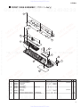
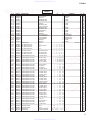
1
http://www.xiaoyu163.com QQ 376315150 892498299 SERVICE MANUAL TEL TEL 13942296513 13942296513 CONTENTS(目次) www x iao y u163. com • OPTION(別売品) MAT1 ED 011962 . SPECIFICATIONS(総合仕様)...................................3/4 PANEL LAYOUT(パネルレイアウト)...........................5 CIRCUIT BOARD LAYOUT(ユニットレイアウト) ..........6 WIRING(結線図) ............................................................8 DISASSEMBLY PROCEDURE(分解手順)...................9 LSI PIN DESCRIPTION(LSI 端子機能表)..................14 IC BLOCK DIAGRAM(IC ブロック図).......................16 CIRCUIT BOARDS(シート基板図)............................18 TEST PROGRAM(テストプログラム)..................24/37 SAVING and LOADING A FILE (ファイルのセーブ&ロード)..................................50/53 UPDATING(アップデート)........................................56 FORMAT OF USB MEMORY DEVICE (USB 記憶装置のフォーマット(初期化))..................58 INITIAL FACTORY SETTING (ファクトリーセット)..................................................59 DISPLAY MESSAGES(メッセージリスト)..........60/62 BOOT SEQUENCE(起動シーケンス)...................64/65 PARTS LIST BLOCK DIAGRAM(ブロックダイアグラム) CIRCUIT DIAGRAM(回路図) DTX-MULTI12 20091125-94500 MAT1 20091125-5250 HAMAMATSU, JAPAN Copyright (c) Yamaha Corporation. All rights reserved. PDF & ’09.11 376315150 892498299 376315150 892498299 QQ 376 315150 8924 98299 QQ QQ TEL 13942296513 http://www.xiaoyu163.com DTX-MULTI 12 QQ 376315150 IMPORTANT NOTICE 892 498 29 9 This manual has been provided for the use of authorized Yamaha Retailers and their service personnel. It has been assumed that basic service procedures inherent to the industry, and more specifically Yamaha Products, are already known and understood by the users, and have therefore not been restated. WARNING : Failure to follow appropriate service and safety procedures when servicing this product may result in personal injury, destruction of expensive components and failure of the product to perform as specified. For these reasons, we advise all Yamaha product owners that all service required should be performed by an authorized Yamaha Retailer or the appointed service representative. IMPORTANT : This presentation or sale of this manual to any individual or firm does not constitute authorization certification, recognition of any applicable technical capabilities, or establish a principal-agent relationship of any form. The data provided is belived to be accurate and applicable to the unit(s) indicated on the cover. The research engineering, and service departments of Yamaha are continually striving to improve Yamaha products. Modifications are, therefore, inevitable and changes in specification are subject to change without notice or obligation to retrofit. Should any discrepancy appear to exist, please contact the distributor’s Service Division. Static discharges can destroy expensive components. Discharge any static electricity your body may have accumulated by grounding yourself to the ground bus in the unit (heavy gauge black wires connect to this bus.) IMPORTANT : Turn the unit OFF during disassembly and parts replacement. Recheck all work before you apply power to the unit. DO NOT PLACE SOLDER, ELECTRICAL/ELECTRONIC OR PLASTIC COMPONENTS IN YOUR MOUTH FOR ANY REASON WHAT SO EVER! Avoid prolonged, unprotected contact between solder and your skin! When soldering, do not inhale solder fumes or expose eyes to solder/ flux vapor! If you come in contact with solder or components located inside the enclosure of this product, wash your hands before handling food. 376315150 892498299 IMPORTANT. The wires in this mains lead are coloured in accordance with the following code: BLUE : NEUTRAL BROWN : LIVE As the colours of the wires in the mains lead of this apparatus may not correspond with the coloured markings identifying the terminals in your plug proceed as follows: The wire which is coloured BLUE must be connected to the terminal which is marked with the letter N or coloured BLACK. The wire which is coloured BROWN must be connected to the terminal which is marked with the letter L or coloured RED. Making sure that neither core is connected to the earth terminal of the three pin plug. • This applies only to products distributed by Yamaha Music U.K. Ltd. (2 wires) WARNING Components having special characteristics are marked originally installed. and must be replaced with parts having specification equal to those 印の部品は、安全を維持するために重要な部品です。交換する場合は、安全のために必ず指定の部品をご使用ください。 SAVING DATA(データの保存) Saving and backing up your data 作成したデータの保存とバックアップ Saved data may be lost due to malfunction or incorrect operation. Save important data to external USB storage device. 保存したデータは故障や誤操作などのために失われ ることがあります。大切なデータは USB 記憶装置 に保存してください。 www Be sure to perform it 2 x iao y u163. com 必ず実行 Backing up the USB storage device 外部 USB 記憶装置のバックアップ To protect against data loss through media damage, we recommend that you save your important data onto two USB storage devices. 保存した USB 記憶装置の万一の事故に備えて、大 切なデータは予備の USB 記憶装置にバックアップ として保存されることをおすすめします。 . 376315150 892498299 QQ 376 315150 8924 98299 TEL 13942296513 QQ QQ IMPORTANT NOTICE FOR THE UNITED KINGDOM Connecting the Plug and Cord 13942296513 13942296513 WARNING: This product contains chemicals known to the State of California to cause cancer, or birth defects or other reproductive harm. TEL TEL WARNING : http://www.xiaoyu163.com DTX-MULTI 12 QQ 376315150 892498299 SPECIFICATIONS Pad section Tone generator Trigger section 5 (three-zone x 1; monaural x 4) Maximum polyphony 64 notes Wave memory Voices 100 MB (16-bit linear conversion) Drum and percussion: 1,061 Keyboard: 216 Drum kits Preset: 50 User-defined: 200 Effects Variation x 42 types; Chorus x 6 types; Reverb x 6 types: 5-band master equalizer Pad functions Increment or decrement of drum kit, pattern, or tempo; tap tempo; switching on or off of click-track; transmission of control change messages Readable quantity 500 Bit depth 16 bit Wave memory 64 MB Maximum size Mono sample: 2 MB Stereo sample: 4 MB Sample formats Proprietary, WAV, and AIFF Sequence capacity 152,000 notes Quarter note / 480 Recording method Real-time overdubbing Patterns Preset patterns: 128 phrases (including 3 demo patterns) User-defined patterns: 50 phrases Sequence formats Proprietary SMF Format 0 (for loading only) Click-track Other www Tempo QQ 376 315150 8924 98299 30 to 300 BPM. Tap tempo functionality Beats 1/4 – 16/4, 1/8 – 16/8, 1/16 – 16/16 Note timing Accent notes, quarter notes, eight notes, sixteenth notes, triplets Display Backlit LCD with 2 rows of 16 characters Connectors PAD M jack (standard stereo-phone plug; left = trigger, right = rim switch) PAD N/O and PAD P/Q jacks (standard stereo-phone plug; left = trigger, right = trigger) HI-HAT CONTROL jack (standard stereo-phone plug) FOOT SW jack (standard stereo-phone plug) OUTPUT L/MONO and R jacks (standard phone plugs) PHONES jack (standard stereo-phone plug), AUX IN jack (standard stereo-phone plug), MIDI IN and OUT connectors, USB TO HOST port, USB TO DEVICE port, and DC IN. Power Consumption 9W (DTXM12 and PA-5D adaptor) 6W (DTXM12 and PA-150 adaptor) Size and weight 345 (w) x 319 (d) x 96 (h) mm; 3.3 kg Package Contents Power adaptor (PA-5D/PA-150 or an equivalent recommended by Yamaha), Owner’s Manual (this booklet), Data List booklet, DVD-ROM . 376315150 892498299 376315150 892498299 TEL 13942296513 QQ QQ Note resolution 13942296513 13942296513 Sequencer 12 External inputs TEL TEL Waves Built-in pads x iao y u163. com 3 http://www.xiaoyu163.com DTX-MULTI 12 QQ 376315150 892498299 総合仕様 パッド部 音源部 パッド数 12 外部入力 5 (3ゾーン対応×1, モノラル× 4) 最大同時発音数 64音 波形メモリー ボイス数 100MB相当(16bitリニア換算) ドラム/パーカッション:1,061音色 キーボード:216音色 ドラムキット数 プリセット:50キット ユーザー:200キット ウェーブ 読み込み可能ウェーブ数 500 ウェーブデータビット 16bit 波形メモリー 64MB 最大サンプルサイズ 1モノサンプル:2MB 1ステレオサンプル:4MB サンプルフォーマット オリジナルフォーマット、WAV、AIFF シーケンサー容量 約152,000音 13942296513 シーケンサー クリック 4分音符/480 レコーディング方式 リアルタイムオーバーダビング パターン数 プリセットパターン128曲 (うちデモ3曲) ユーザーパターン:50曲 シーケンスフォーマット オリジナルフォーマット SMFフォーマット0 (ロードのみ ) テンポ 30∼300/分、タップテンポ機能 ビート 1/4 ∼ 16/4、1/8 ∼ 16/8、1/16 ∼ 16/16 16文字 x 2行 バックライト付きLCD 接続端子 トリガー入力 M (ステレオ標準フォーン端子 L:トリガー、R:リムスイッチ) トリガー入力 N/O、P/Q (ステレオ標準フォーン端子 L:トリガー、R:トリガー ) HI-HAT CONTROL (ステレオ標準フォーン端子) OUTPUT L/MONO、R (標準フォーン端子) FOOT SW (ステレオ標準フォーン端子)、PHONES (ステレオ標準フォーン端子)、 AUX IN (ステレオ標準フォーン端子) MIDI IN/OUT、USB (TO HOST、TO DEVICE)、DC IN 消費電力 PA-5D使用時:9W (DTXM12および電源アダプター ) PA-150使用時:6W (DTXM12および電源アダプター ) 寸法、重量 345(W)×319(D)×96(H)mm 、3.3kg 付属品 電源アダプター (PA-5D/PA-150または同等のヤマハ推奨品 )、保証書、取扱説明書(本書)、 データリスト、DVD-ROM×1枚 376315150 892498299 www 4 . x iao y u163. com 376315150 892498299 アクセント、4分音符、8分音符、16分音符、3連符 ディスプレイ TEL 13942296513 その他 QQ 376 315150 8924 98299 タイミング QQ QQ 音符分解能 13942296513 ドラムキットINC/DEC、パターンINC/DEC、テンポ INC/DEC、タップテンポ、クリックON/ OFF、コントロールチェンジ送信 TEL バリエーション×42タイプ、コーラス×6タイプ、リバーブ×6タイプ、マスター EQ(5バンド) パッドファンクション TEL エフェクター トリガー部 http://www.xiaoyu163.com DTX-MULTI 12 QQ 376315150 892498299 PANEL LAYOUT(パネルレイアウト) • Front Panel(フロントパネル) q w e r t !1 !2 !3 !5 ≤≤≤≤≤YAMAHA <<DTX-MULTI≤12>> u i o !0 !4 !6 TEL TEL y !7 13942296513 !8 !9 @1 [VOLUME] dial Display Pad Indicator [MIDI] button [VOICE] button [KIT] button [PTN] button [WAVE] button [UTILITY] button [SHIFT] button [ ] button [EXIT] button [ENTER] button [STORE] button [ < ] [ ] [ > ] button [-/DEC] button !7 !8 !9 @0 @1 @2 @3 @4 @5 @6 @7 @8 @9 #0 #1 @4 [+/INC] button [USB TO DEVICE] port [USB TO HOST] port [ Standby/On] switch Cord clip [DC IN] terminal [MIDI IN/OUT] connectors [FOOT SW] jack [HI-HAT CONTROL] jack [PAD] jacks (!3 to !7) [AUX IN] jack [GAIN] knob [OUTPUT L/MONO and R] jacks [PHONES] jack [VOLUME] knob @5 @6 q w e r t y u i o !0 !1 !2 !3 !4 !5 !6 @7 @8 @9 VOLUME(マスターボリューム) LCD 画面 LED パッドインジケーター [MIDI] ボタン [VOICE] ボタン [KIT] ボタン [PTN] ボタン [WAVE] ボタン [UTILITY] ボタン [SHIFT] ボタン [ ](クリック)ボタン [EXIT] ボタン [ENTER] ボタン [STORE] ボタン [<]、[ ]、[>](セレクト)ボタン [‒/DEC] ボタン #0 #1 !7 !8 !9 @0 @1 @2 @3 @4 @5 @6 @7 @8 @9 #0 #1 [+/INC] ボタン [USB TO DEVICE] 端子 [USB TO HOST] 端子 [ (スタンバイ / オン)] スイッチ コードフック [DC IN] 端子 [MIDI IN/OUT] 端子 [FOOT SW] 端子 [HH CTRL(ハイハットコントロール)] 端子 [ トリガー入力端子 ](!3 ∼ !7) [AUX IN] 端子 [GAIN] ノブ [OUTPUT L/MONO、R] 端子 [PHONES] 端子 [VOLUME(ヘッドフォンボリューム)] ノブ x iao y u163. com > > . @3 > www @2 QQ 376 315150 8924 98299 376315150 892498299 376315150 892498299 q w e r t y u i o !0 !1 !2 !3 !4 !5 !6 @0 QQ QQ Panel(リアパネル) TE•LRear13942296513 > 13942296513 • Side Panel(サイドパネル) 5 http://www.xiaoyu163.com DTX-MULTI 12 QQ 376315150 892498299 CIRCUIT BOARD LAYOUT(ユニットレイアウト) <Top view> PAD UNIT R (パッドユニットR) TEL TEL 13942296513 13942296513 PAD UNIT F (パッドユニットF) QQ 376 315150 8924 98299 <Top view> JK DM www 6 . x iao y u163. com 376315150 892498299 376315150 892498299 TEL 13942296513 QQ QQ FRONT CASE ASSEMBLY (フロントAss’ y) http://www.xiaoyu163.com DTX-MULTI 12 QQ 376315150 892498299 • FRONT CASE ASSEMBLY (フロントAss’y) LCD MODULE (LCDモジュール) <Bottom view> VR PN • PAD UNIT R (F) (パッドユニットR(F)) PAD ASSEMBLY (パッドユニット組立品) TEL TEL <Bottom view> 13942296513 13942296513 <Top view> <Bottom view> www PAD SHEET SWITCH (パッドシートSW) SENSOR UNIT CT (センサユニットCT) x iao y u163. com SENSOR UNIT ST (センサユニットST) . QQ 376 315150 8924 98299 376315150 892498299 376315150 892498299 • PAD ASSEMBLY (パッドユニット組立品) QQ QQ TEL 13942296513 SENSOR UNIT ST (センサユニットST) 7 http://www.xiaoyu163.com 892498299 to SENSOR UNIT ST (PAD1) to PAD SHEET SWITCH (Rear side) to SENSOR UNIT ST (PAD4) to SENSOR UNIT CT (PAD5) CN303 (37P) CN6 (17P) CN8 (37P) CN308 (2P) CN309 (2P) CN310 (2P) QQ 3 7 6 3 1 5 1 5 0 8 9 2 4 9 8 2 9 9 CN305 (2P) CN306 (2P) CN307 (2P) CN7 (10P) DM CN5 (26P) CN4 (16P) CN601 (8P) www VR CN501 (26P) x ia o y u 1 6 3 . c o m LCD MODULE (LCDモジュール) . PN http://www.xiaoyu163.com 376315150 892498299 376315150 892498299 TE L 1 3 9 4 2 2 9 6 5 1 3 to SENSOR UNIT ST (PAD6) CN301 (10P) QQ QQ CN302 (17P) CN311 (21P) CN312 (21P) 13942296513 13942296513 JK CN304 (8P) TEL TEL to PAD SHEET SWITCH (Front side) WIRING(結線図) to SENSOR UNIT CT (PAD2) DTX-MULTI 12 8 QQ 3 7 6 3 1 5 1 5 0 to SENSOR UNIT ST (PAD3) http://www.xiaoyu163.com DTX-MULTI 12 QQ 376315150 892498299 DISASSEMBLY PROCEDURE(分解手順) Precautions(注意事項) * ※ フラットケーブルの注意 接点が裏面から透けて見えます。コネクタにケーブルの表・ 裏を逆に差込まないように注意して取り付けてください。 (写真 1) Notes on Flat Cable Contacts are visible from the back. Pay attention not to insert and install the cable to the connector inversely. (Photo 1) Front Side(表面) Back Side(裏面) TEL TEL Photo 1(写真 1) PAD UNIT R (Time required: About 1 minutes) 1. パッドユニット R(所要時間 : 約 1 分) Remove the four (4) screws marked [150A] and three (3) screws marked [160A]. The pad unit R can then be removed. (Fig.1, Fig.2) 1-1 [150A] のネジ 4 本と [160A] のネジ 3 本を外して、 パッドユニット R を外します。 (図 1、図 2) <Left side view> 13942296513 13942296513 1. 1-1 <Right side view> [150A] [150A] [150B] QQ QQ [150B] 376315150 892498299 376315150 892498299 QQ 376 315150 8924 98299 TEL 13942296513 [150]: BIND HEAD TAPPING SCREW-S (Sタイト+BIND) 3.0X6 MFZN2B3 (WE87780R) Fig.1(図1) <Bottom view> [160A] <Top view> [160A] [160A] PAD UNIT R (パッドユニット R) [160B] [160B] www [160C] . x iao y u163. com [160C] KNOB V (Vツマミ) PAD UNIT F (パッドユニット F) [160]: BIND HEAD SCREW (小ネジ+BIND) 3.0X6 MFZN2B3 (WE878300) Fig.2(図2) 9 http://www.xiaoyu163.com DTX-MULTI 12 QQ 376315150 892498299 2. パッドユニット F(所要時間 : 約 3 分) Remove the pad unit R. (See procedure 1.) Remove the four (4) screws marked [150B] and six (6) screws marked [160B]. The pad unit F can then be removed. (Fig.1, Fig.2) 2-1 2-2 パッドユニット R を外します。 (1 項参照) [150B] のネジ 4 本と [160B] のネジ 6 本を外して、 パッドユニット F を外します。 (図 1、図 2) 3. JK Circuit Board 3. JK シート(所要時間 : 約 5 分) (Time required: About 5 minutes) Remove the pad unit R. (See procedure 1.) Remove the pad unit F. (See procedure 2.) Remove the five (5) screws marked [130A] and screw marked [170]. The JK sheet assembly can then be removed. (Fig.3) 3-1 3-2 3-3 パッドユニット R を外します。 (1 項参照) パッドユニット F を外します。 (2 項参照) [130A] のネジ 5 本と [170] のネジ 1 本を外して、 JK シート Ass’ y を外します。(図 3) ※ [170] のネジを外す際は、DC コードコラムを紛失しな いよう注意してください。(図 3) 3-4 [JK60] のネジ 1 本を外して、DC アングルを外し ます。(図 4) TEL 3-1 3-2 3-3 13942296513 * 3-4 Pay attention not to lose DC cord column when removing the screw marked [170]. (Fig. 3) Remove the screw marked [JK60]. The DC angle can then be removed. (Fig.4) <Rear view> DC CORD COLUMN (DCコードコラム) [170] <Top view> [130A] JK SHEET ASSEMBLY (JKシートAss’ y) [130A] [130C] www x iao y u163. com [130B] . EARTH PLATE (アース金具) FRONT CASE ASSEMBLY (フロントAss’y) DM [130B] [130]: BIND HEAD TAPPING SCREW-B (Bタイト+BIND) 3.0X8 MFZN2W3 (WE774301) [170]: BIND HEAD TAPPING SCREW-B (Bタイト+BIND) 3.0X12 MFZN2B3 (WE99810R) 10 Fig.3(図3) 376315150 892498299 376315150 892498299 QQ 376 315150 8924 98299 QQ QQ TEL 13942296513 13942296513 PAD UNIT F (Time required: About 3 minutes) 2-1 2-2 TEL 2. http://www.xiaoyu163.com DTX-MULTI 12 QQ 376315150 892498299 3-5 3-6 * Remove the two (2) screws marked [JK40] and five (5) angle brackets, U and separate the JK circuit board and shield JK. (Fig. 4) Remove the push button from the JK circuit board. (Fig. 4) 3-5 3-6 フロント Ass’y(所要時間 : 約 4 分) 4-1 4-2 4-3 (Time required: About 4 minutes) Remove the pad unit R. (See procedure 1.) Remove the pad unit F. (See procedure 2.) Remove the three (3) screws marked [130B] and four (4) screws marked [160C]. The front case assembly can then be removed. (Fig.2, Fig.3) パッドユニット R を外します。 (1 項参照) パッドユニット F を外します。 (2 項参照) [130B] のネジ 3 本と [160C] のネジ 4 本を外して、 フロント Ass’ y を外します。(図 2、図 3) 5. DM Circuit Board 5. DM シート(所要時間 : 約 5 分) (Time required: About 5 minutes) Remove the pad unit R. (See procedure 1.) Remove the pad unit F. (See procedure 2.) Remove the front case assembly. (See procedure 4.) Remove the four (4) screws marked [130C] and remove the DM circuit board with the shield DM. 5-1 5-2 5-3 5-4 5-1 5-2 5-3 5-4 パッドユニット R を外します。 (1 項参照) パッドユニット F を外します。 (2 項参照) フロント Ass’ y を外します。(4 項参照) [130C] のネジ 4 本を外して、シールド DM が付 いた状態の DM シートを外します。 (図 3) ※ [130C] のネジを外す際は、アース金具を紛失しないよ う注意してください。(図 3) 5-5 [140] のネジ 4 本を外して、DM シートとシール ド DM を分離します。(図 5) QQ 376 315150 8924 98299 TEL 13942296513 * Pay attention not to lose earth plate when removing the screws marked [130C]. 5-5 Remove the four (4) screws marked [140] and separate the DM circuit board and shield DM. (Fig. 5) • JK SHEET ASSEMBLY(JKシートAss’y) DC ANGLE (DCアングル) 376315150 892498299 376315150 892498299 4. 4-1 4-2 4-3 QQ QQ Front Case Assembly SHIELD DM (シールドDM) JK [JK60] [JK40] PUSH BUTTON (プッシュボタン) ANGLE BRACKET, U (U字金具) www DM x iao y u163. com SHIELD JK (シールドJK) [JK40]: BIND HEAD TAPPING SCREW-B (Bタイト+BIND) 3.0X12 MFZN2W3 (WE98740R) [JK60]: BIND HEAD TAPPING SCREW-S (Sタイト+BIND) 3.0X6 MFZN2W3 (WE877900) . Fig.4(図4) 13942296513 13942296513 プッシュボタンは JK シートの構成部品ではありません。 JK シートを交換する際には、本体のシートからプッシュ ボタンを取り外して、新しいシートに取り付けてくださ い。(図 4) TEL TEL ※ The push button is not part of the JK circuit board. When replacing the JK circuit board, remove the push button from the circuit board and install it on the new circuit board. (Fig. 4) 4. [JK40] のネジ 2 本と U 字金具 5 個を外して、 JK シー トとシールド JK を分離します。 (図 4) JK シートからプッシュボタンを外します。(図 4) [140] [140]: BIND HEAD TAPPING SCREW-S (Sタイト+BIND) 3.0X6 MFZN2W3 (WE877900) Fig.5(図5) 11 http://www.xiaoyu163.com DTX-MULTI 12 QQ 376315150 892498299 6. 6. PN Circuit Board, LCD Module, VR Circuit Board パッドユニット R を外します。 (1 項参照) パッドユニット F を外します。 (2 項参照) フロント Ass’ y を外します。(4 項参照) PN シート(所要時間 : 約 5 分) [80A] のネジ 3 本を外して、シールド PN を外し ます。(図 6) 6-4-2 [80B] のネジ 3 本を外して、PN シートを外します。 (図 6) 6-1 6-2 6-3 6-4 ※ 6-5 QQ 376 315150 8924 98299 [80A] a KNOB (Vツマミ) [80B] c b PN SHIELD PN (シールドPN) [90] Fig.7(図7) LCD MODULE (LCDモジュール) [80C] www x iao y u163. com VR . [80]: BIND HEAD TAPPING SCREW-B (Bタイト+BIND) 3.0X8 MFZN2W3 (WE774301) [90]: BIND HEAD TAPPING SCREW-B (Bタイト+BIND) 2.6X10 MFZN2W3 (WF741100) 12 Fig.6(図6) 376315150 892498299 376315150 892498299 • FRONT CASE ASSEMBLY(フロントAss’y) QQ QQ TEL 13942296513 13942296513 13942296513 LCD モジュール(所要時間 : 約 5 分) [90] のネジ 4 本を外して、LCD モジュールを外し ます。(図 6) 6-6 VR シート(所要時間 : 約 4 分) 6-6-1 V ツマミを外します。 (図 2、図 7) 6-6-2 [80C] のネジ 1 本を外して、VR シートを外します。 (図 6) 6-5 6-5-1 Tighten the screws in the order of a, b and c in Fig. 6 when installing the PN circuit board to front case. (Fig. 6) LCD Module (Time required: About 5 minutes each) 6-5-1 Remove the four (4) screws marked [90]. The LCD module can then be removed. (Fig. 6) 6-6 VR Circuit Board (Time required: About 4 minutes each) 6-6-1 Remove the knob V. (Fig. 2, Fig. 7) 6-6-2 Remove the screw marked [80C]. The VR circuit board can then be removed. (Fig. 6) PN シートをフロントケースへ取り付ける際は、図 6 の a, b, c の順でネジ締めをしてください。(図 6) TEL TEL Remove the pad unit R. (See procedure 1.) Remove the pad unit F. (See procedure 2.) Remove the front case assembly. (See procedure 4.) PN Circuit Board (Time required: About 5 minutes each) 6-4-1 Remove the three (3) screws marked [80A]. The shield PN can then be removed. (Fig. 6) 6-4-2 Remove the three (3) screws marked [80B]. The PN circuit board can then be removed. (Fig. 6) * PN シート、LCD モジュール、VR シート 6-1 6-2 6-3 6-4 6-4-1 http://www.xiaoyu163.com DTX-MULTI 12 QQ 376315150 892498299 7. Sensor Unit CT, Sensor Unit ST, Pad Sheet Switch (Time required: About 2 minutes each) * The following describes procedures for pad unit R side. Removal on pad unit F side can be conducted in the same way. 7-1 7-2 ※ ここでは、パッドユニット R 側の手順を記載します。 パッドユニット F 側も同様に外すことができます。 7-1 7-2 パッドユニット R を外します。 (1 項参照) [50] のネジ 10 本を外して、パッド支板 R を外し ます。(図 8) センサユニット CT、センサユニット ST センサユニット CT またはセンサユニット ST を 外します。(図 9) パッドシート SW ラバーパッドを外します。(図 9、写真 2) 6 個所のピンを外しながら、パッドシート SW を 外します。(写真 3) 7-3 7-3-1 7-4 7-4-1 7-4-2 • PAD UNIT R(パッドユニットR) <Bottom view> RUBBER PAD (ラバーパッド) [50] [50] [50] [50] QQ 376 315150 8924 98299 376315150 892498299 376315150 892498299 TEL 13942296513 QQ QQ PAD ASSEMBLY (パッド組立品) [50] 13942296513 13942296513 センサユニット CT、センサユニット ST、 パッドシート SW(所要時間 : 各約 2 分) TEL TEL Remove the pad unit R. (See procedure 1.) Remove the ten (10) screws marked [50]. The pad support plate R can then be removed. (Fig. 8) 7-3 Sensor Unit CT, Sensor Unit ST 7-3-1 Remove the sensor unit CT or sensor unit ST. (Fig. 9) 7-4 Pad Sheet Switch 7-4-1 Remove the rubber pad. (Fig. 9, Photo 2) 7-4-2 Remove the pins at six (6) positions to remove the pad sheet switch. (Photo 3) 7. [50] PAD SUPPORT PLATE R (パッド支板R) Photo 2(写真2) [50]: PW HEAD TAPPING SCREW-P (Pタイト+PWH) 3.0X10⁻¹⁰ MFZN2W3 (WF76550R) Fig.8(図8) Pin (ピン) Pin (ピン) Pin (ピン) • PAD ASSEMBLY(パッド組立品) RUBBER PAD (ラバーパッド) <Bottom view> www x iao y u163. com PAD SHEET SWITCH (パッドシートSW) Photo 3(写真3) SENSOR UNIT ST (センサユニットST) . SENSOR UNIT CT (センサユニットCT) SENSOR UNIT ST (センサユニットST) Fig.9(図9) 13 http://www.xiaoyu163.com DTX-MULTI 12 QQ 376315150 892498299 LSI PIN DESCRIPTION(LSI 端子機能表) R8A02032BG (X8810A00) CPU (SWX02) PIN NO. VSS AN2 AN1 VSS RxD1 SCK1 UCLK VSS FUNC_DM VSS HOST_DM POWER_ENB XTAL EXTAL VSS CS7N/PJ6 TRSTN TDI TCK VCCQ MD15 VSS AN3 AN0 VSS TxD1 TxD0 VSS FUNC_DP VSS HOST_DP SCL VSS VSS CS4N/PJ3 TIOC0A/PJ7 TESTN TMS VCCQ VCCQ MD13 MD14 VSS VREFADC VSSADC VSS RxD0 VSS VBUS VSS OVER_CURRENT_N SDA CS0N CS2N/PJ1 CS5N/PJ4 ASEMDN TDO VCCQ VDDPLL VDDPLL MD10 MD11 MD12 VSS VCCADC VSS RESN VCCQ PULLUP_ENB VCCQ UCTL EICN CS1N/PJ0 CS3N/PJ2 CS6N/PJ5 ASEBRKAKN VCCQ VCCQ VSSPLL I I I I I I/O I/O O O I O I I I I/O I I O O I/O I/O I/O O O I I I/O I/O I I I I/O O O O I O I/O I/O I/O I O I O O O O I/O - Ground ADC analog input 2 ADC analog input 1 Ground Serial input 1 External sync. clock input 1 USB external clock input (48 MHz) Ground USB function data Ground USB host data USB voltage enable Crystal oscillator output Crystal oscillator input (16.9344 MHz) Ground SH2A-CPU chip select 7 JTAG test reset input JTAG test data input JTAG test clock input Power supply +3.3 V Wave memory data bus 15 Ground ADC analog input 3 ADC analog input 0 Ground Serial output 1 Serial output 0 Ground USB function data + Ground USB host data + E bus (I2C) clock input/output (5V compatible) 376315150 892498299 TEL 13942296513 www 14 . Ground SH2A-CPU chip select 4 PWM output Test input JTAG test mode select input Wave memory data bus 13 Wave memory data bus 14 Ground ADC reference power supply +3.3 V ADC analog ground Ground Serial input 0 Ground USB cable connection monitor (5V compatible) Ground USB overcurrent detection (5V compatible) E bus (I2C) data input/output (5V compatible) SH2A-CPU chip select 0 SH2A-CPU chip select 2 SH2A-CPU chip select 5 Debug mode configuration JTAG test data output Power supply +3.3 V Wave memory data bus 10 Wave memory data bus 11 Wave memory data bus 12 Ground ADC analog power supply +3.3 V Ground Hardware reset Power supply +3.3 V USB pull-up enable Power supply +3.3 V USB output control E bus reset output SH2A-CPU chip select 1 SH2A-CPU chip select 3 SH2A-CPU chip select 6 Emulator break OUTER NO. NAME I/O 80 81 82 83 84 85 86 87 88 89 90 91 92 93 94 95 96 97 98 99 100 101 102 103 104 105 106 107 108 109 110 111 112 113 114 115 116 117 118 119 120 121 122 123 124 125 126 127 128 129 130 131 132 133 134 135 136 137 138 139 140 141 142 143 144 145 146 147 148 149 150 151 152 153 154 155 156 157 158 D20 E1 E2 E3 E4 E5 E6 E7 E8 E9 E10 E11 E12 E13 E14 E15 E16 E17 E18 E19 E20 F1 F2 F3 F4 F5 F16 F17 F18 F19 F20 G1 G2 G3 G4 G5 G16 G17 G18 G19 G20 H1 H2 H3 H4 H5 H16 H17 H18 H19 H20 J1 J2 J3 J4 J5 J9 J10 J11 J12 J16 J17 J18 J19 J20 K1 K2 K3 K4 K5 K9 K10 K11 K12 K16 K17 K18 K19 K20 VSSPLL MD6 MD7 MD8 MD9 VDD VDD VSS VCCQ VSS VCCQ VCCQ VSS VCCQ VSS VDD VDD D31/PF7 D30/PF6 D29/PF5 D28/PF4 MD2 MD3 MD4 MD5 VDD VDD D27/PF3 D26/PF2 D25/PF1 D24/PF0 MA2 MA1 MD0 MD1 VSS VSS D23/PE7 D22/PE6 D21/PE5 D20/PE4 MA6 MA5 MA4 MA3 VCCQ VCCQ D19/PE3 D18/PE2 VCCQ VCCQ MA10 MA9 MA8 MA7 VSS VSS VSS VSS VSS VSS D17/PE1 D16/PE0 CKOEN CKIO MA14 MA13 MA12 MA11 VDD VSS VSS VSS VSS VDD CKE D15 VSS VSS I/O I/O I/O I/O I/O I/O I/O I/O I/O I/O I/O I/O I/O I/O I/O I/O O O I/O I/O I/O I/O I/O I/O O O O O I/O I/O O O O O I/O I/O I O O O O O O I/O - FUNCTION PLL analog ground Wave memory data bus 6 Wave memory data bus 7 Wave memory data bus 8 Wave memory data bus 9 Power supply +1.2 V Ground Power supply +3.3 V Ground Power supply +3.3 V Ground Power supply +3.3 V Ground Power supply +1.2 V SH2A-CPU data bus 31 SH2A-CPU data bus 30 SH2A-CPU data bus 29 SH2A-CPU data bus 28 Wave memory data bus 2 Wave memory data bus 3 Wave memory data bus 4 Wave memory data bus 5 Power supply +1.2 V SH2A-CPU data bus 27 SH2A-CPU data bus 26 SH2A-CPU data bus 25 SH2A-CPU data bus 24 Wave memory address bus 2 Wave memory address bus 1 Wave memory data bus 0 Wave memory data bus 1 QQ 376 315150 8924 98299 Power supply +3.3 V PLL analog power supply +1.2 V PIN NO. Ground SH2A-CPU data bus 23 SH2A-CPU data bus 22 SH2A-CPU data bus 21 SH2A-CPU data bus 20 Wave memory address bus 6 Wave memory address bus 5 Wave memory address bus 4 Wave memory address bus 3 Power supply +3.3 V SH2A-CPU data bus 19 SH2A-CPU data bus 18 Power supply +3.3 V Wave memory address bus 10 Wave memory address bus 9 Wave memory address bus 8 Wave memory address bus 7 Ground SH2A-CPU data bus 17 SH2A-CPU data bus 16 Clock output control for SDRAM Clock output for SDRAM Wave memory address bus 14 Wave memory address bus 13 Wave memory address bus 12 Wave memory address bus 11 Power supply +1.2 V x iao y u163. com Power supply +3.3 V PLL analog ground Ground Power supply +1.2 V Clock enable for SDRAM SH2A-CPU data bus 15 Ground 376315150 892498299 A1 A2 A3 A4 A5 A6 A7 A8 A9 A10 A11 A12 A13 A14 A15 A16 A17 A18 A19 A20 B1 B2 B3 B4 B5 B6 B7 B8 B9 B10 B11 B12 B13 B14 B15 B16 B17 B18 B19 B20 C1 C2 C3 C4 C5 C6 C7 C8 C9 C10 C11 C12 C13 C14 C15 C16 C17 C18 C19 C20 D1 D2 D3 D4 D5 D6 D7 D8 D9 D10 D11 D12 D13 D14 D15 D16 D17 D18 D19 DM: IC8 FUNCTION QQ QQ I/O 13942296513 13942296513 NAME TEL TEL 1 2 3 4 5 6 7 8 9 10 11 12 13 14 15 16 17 18 19 20 21 22 23 24 25 26 27 28 29 30 31 32 33 34 35 36 37 38 39 40 41 42 43 44 45 46 47 48 49 50 51 52 53 54 55 56 57 58 59 60 61 62 63 64 65 66 67 68 69 70 71 72 73 74 75 76 77 78 79 OUTER NO. http://www.xiaoyu163.com DTX-MULTI 12 QQ 376315150 892498299 159 160 161 162 163 164 165 166 167 168 169 170 171 172 173 174 175 176 177 178 179 180 181 182 183 184 185 186 187 188 189 190 191 192 193 194 195 196 197 198 199 200 201 202 203 204 205 206 207 208 209 210 211 212 213 214 215 216 217 218 219 220 221 222 223 224 225 226 227 228 229 230 231 232 233 234 235 236 237 L1 L2 L3 L4 L5 L9 L10 L11 L12 L16 L17 L18 L19 L20 M1 M2 M3 M4 M5 M9 M10 M11 M12 M16 M17 M18 M19 M20 N1 N2 N3 N4 N5 N16 N17 N18 N19 N20 P1 P2 P3 P4 P5 P16 P17 P18 P19 P20 R1 R2 R3 R4 R5 R16 R17 R18 R19 R20 T1 T2 T3 T4 T5 T6 T7 T8 T9 T10 T11 T12 T13 T14 T15 T16 T17 T18 T19 T20 U1 MA15 MA16 MA17 MA18 VDD VSS VSS VSS VSS VDD D11 D12 D13 D14 MA19 MA20 MA21 MA22 VSS VSS VSS VSS VSS VSS D7 D8 D9 D10 MA23/PG4 MA24/PG5 MA25/PG6 MA26/PG7 VCCQ VCCQ D3 D4 D5 D6 MCS3N/PG3 MCS2N/PG2 MCS1N/PG1 MWRN/PG0 VSS VSS RD/WRN D0 D1 D2 MCS0N MRDN BTCHG PA0 VDD VDD WE3N/DQMUU/PH3 RASLN CASLN RDN PA1 PA2 PA3 PA4 VDD VDD VSS VCCQ VSS VCCQ VCCQ VSS VCCQ VSS VDD VDD A0/PH4 WE0N/DQMLL/PH0 WE1N/DQMLU/PH1 WE2N/DQMUL/PH2 PA5 O O O O I/O I/O I/O I/O O O O O I/O I/O I/O I/O O O O O I/O I/O I/O I/O O O O O O I/O I/O I/O O O I I/O O O O O I/O I/O I/O I/O O O O O I/O FUNCTION Wave memory address bus 15 Wave memory address bus 16 Wave memory address bus 17 Wave memory address bus 18 Power supply +1.2 V Ground Power supply +1.2 V SH2A-CPU data bus 11 SH2A-CPU data bus 12 SH2A-CPU data bus 13 SH2A-CPU data bus 14 Wave memory address bus 19 Wave memory address bus 20 Wave memory address bus 21 Wave memory address bus 22 Ground SH2A-CPU data bus 7 SH2A-CPU data bus 8 SH2A-CPU data bus 9 SH2A-CPU data bus 10 Wave memory address bus 23 Wave memory address bus 24 Wave memory address bus 25 Wave memory address bus 26 TEL 13942296513 www . Power supply +3.3 V SH2A-CPU data bus 3 SH2A-CPU data bus 4 SH2A-CPU data bus 5 SH2A-CPU data bus 6 Wave memory chip select 3 Wave memory chip select 2 Wave memory chip select 1 Wave memory write enable PIN NO. OUTER NO. NAME I/O 238 239 240 241 242 243 244 245 246 247 248 249 250 251 252 253 254 255 256 257 258 259 260 261 262 263 264 265 266 267 268 269 270 271 272 273 274 275 276 277 278 279 280 281 282 283 284 285 286 287 288 289 290 291 292 293 294 295 296 297 298 299 300 301 302 303 304 305 306 307 308 309 310 311 312 313 314 315 316 U2 U3 U4 U5 U6 U7 U8 U9 U10 U11 U12 U13 U14 U15 U16 U17 U18 U19 U20 V1 V2 V3 V4 V5 V6 V7 V8 V9 V10 V11 V12 V13 V14 V15 V16 V17 V18 V19 V20 W1 W2 W3 W4 W5 W6 W7 W8 W9 W10 W11 W12 W13 W14 W15 W16 W17 W18 W19 W20 Y1 Y2 Y3 Y4 Y5 Y6 Y7 Y8 Y9 Y10 Y11 Y12 Y13 Y14 Y15 Y16 Y17 Y18 Y19 Y20 PA6 PA7 VCCQ ED1/PC1 ED5/PC5 ED9/PD1 ED13/PD5 EA2/PK1 ECSN BCLK IRQ0 A25 A21 A17 A13 VCCQ A3 A2 A1 PB0 PB1 VCCQ PB6 ED2/PC2 ED6/PC6 ED10/PD2 ED14/PD6 EA3/PK2 SDI0/PK5 WCLK2/SDO2 IRQ1 BW_MD0 A22/PH5 A18 A14 A10 VCCQ A5 A4 PB2 VCCQ PB4 PB7 ED3/PC3 ED7/PC7 ED11/PD3 ED15/PD7 ERDN/PK3 SDI1/PK6 WCLK SYSCLK2 WAITN/PK7 A23/PH6 A19 A15 A11 A8 VCCQ A6 VCCQ PB3 PB5 ED0/PC0 ED4/PC4 ED8/PD0 ED12/PD4 EA1/PK0 EWRN/PK4 SDO0 SDO1 SYSCLK SYI A24/PH7 A20 A16 A12 A9 A7 VCCQ I/O I/O I/O I/O I/O I/O I I O I O O O O O O O I/O I/O I/O I/O I/O I/O I/O I I O I I O O O O O O I/O I/O I/O I/O I/O I/O I/O I I O O I O O O O O O I/O I/O I/O I/O I/O I/O I I O O O I O O O O O O - FUNCTION Parallel port A6 Parallel port A7 Power supply +3.3 V External CPU data bus 1 External CPU data bus 5 External CPU data bus 9 External CPU data bus 13 External CPU address bus 2 External CPU chip select Bit clock output Interrupt input 0 SH2A-CPU address bus 25 SH2A-CPU address bus 21 SH2A-CPU address bus 17 SH2A-CPU address bus 13 Power supply +3.3 V SH2A-CPU address bus 3 SH2A-CPU address bus 2 SH2A-CPU address bus 1 Parallel port B0 Parallel port B1 Power supply +3.3 V Parallel port B6 External CPU data bus 2 External CPU data bus 6 External CPU data bus 10 External CPU data bus 14 External CPU address bus 3 Serial audio input 0 Word clock output 2/Serial audio output 2 Interrupt input 1 SH2A-CPU data bus width configuration SH2A-CPU address bus 22 SH2A-CPU address bus 18 SH2A-CPU address bus 14 SH2A-CPU address bus 10 Power supply +3.3 V SH2A-CPU address bus 5 SH2A-CPU address bus 4 Parallel port B2 Power supply +3.3 V Parallel port B4 Parallel port B7 External CPU data bus 3 External CPU data bus 7 External CPU data bus 11 External CPU data bus 15 External CPU read enable Serial audio input 1 Word clock output Clock output 2 External wait input SH2A-CPU address bus 23 SH2A-CPU address bus 19 SH2A-CPU address bus 15 SH2A-CPU address bus 11 SH2A-CPU address bus 8 Power supply +3.3 V SH2A-CPU address bus 6 Power supply +3.3 V Parallel port B3 Parallel port B5 External CPU data bus 0 External CPU data bus 4 External CPU data bus 8 External CPU data bus 12 External CPU address bus 1 External CPU write enable Serial audio output 0 Serial audio output 1 Clock output Sync. input from external device SH2A-CPU address bus 24 SH2A-CPU address bus 20 SH2A-CPU address bus 16 SH2A-CPU address bus 12 SH2A-CPU address bus 9 SH2A-CPU address bus 7 Power supply +3.3 V QQ 376 315150 8924 98299 Ground SH2A-CPU read/write enable SH2A-CPU data bus 0 SH2A-CPU data bus 1 SH2A-CPU data bus 2 Wave memory chip select 0 Wave memory read enable BOOT ROM switching control Parallel port A0 Power supply +1.2 V Writing byte of D31 - D24/Selecting D31 - D24 in case of SDRAM RAS output for SDRAM CAS output for SDRAM SH2A-CPU read enable Parallel port A1 Parallel port A2 Parallel port A3 Parallel port A4 Power supply +1.2 V Ground Power supply +3.3 V Ground Power supply +3.3 V Ground Power supply +3.3 V Ground 376315150 892498299 376315150 892498299 I/O QQ QQ NAME 13942296513 13942296513 OUTER NO. TEL TEL PIN NO. x iao y u163. com Power supply +1.2 V SH2A-CPU address bus 0 Writing byte of D7 - D0/Selecting D7 - D0 in case of SDRAM Writing byte of D15 - D8/Selecting D15 - D8 in case of SDRAM Writing byte of D23 - D16/Selecting D23 - D16 in case of SDRAM Parallel port A5 15 http://www.xiaoyu163.com DTX-MULTI 12 QQ 376315150 892498299 IC BLOCK DIAGRAM(IC ブロック図) SN74LV14PWR (X6688A0R) SN74LVC1G32DCKR (X5825A00) SN74LV245APWR (X3693A0R) DM: IC5 JK: IC307 JK: IC319 JK: IC333335 2-Input OR Gate TC74VHCT245AF (XV242B00) Hex Inverter PN: IC501 Octal 3-State Bus Transceiver 20 VCC 2 19 G A2 3 18 B1 5A A3 4 17 B2 5Y A4 5 16 B3 A5 6 15 B4 A6 7 14 B5 A7 8 13 B6 A8 9 12 B7 GND 10 11 B8 14 VDD IN B 1 2 13 6A IN A 2 2A 3 12 6Y GND 3 2Y 4 11 3A 5 10 3Y 6 9 4A GND 7 8 4Y 5 4 Vcc OUT Y FUNCTION TABLE INPUTS A B H X L OUTPUT Y X H L H H L NJM2068M-D-TE2 (X3505A00) NJM2903M(TE1) (X5814A0R) JK: IC331, IC332 JK: IC303, IC312, IC313, IC318, IC320, IC321 JK: IC322 NJM4556AD (XQ824A00) JK: IC308, IC323–330, IC336–339 Differential 4-Channel Multiplexer/Demultiplexer NJM2904M (XV190A00) 1 2Y 2 2Y Y-COM 3 3Y 4 16 VDD 2X 15 2X Y-COM 1X 14 1X 3Y X-COM X-COM 1Y 5 1Y 0X 12 0X INH 6 INH 3X 11 3X VEE 7 A 10 A VSS 8 9 B Output A Inverting Input A Non-Inverting Input A -DC Voltage Supply 1 +V 2 - 3 4 7 + + -V 8 - 6 5 +DC Voltage Supply Output B Inverting Input B Non-Inverting Input B Output A 1 Inverting Input A Non-Inverting Input A 2 +V - 3 Ground + + - 4 8 +DC Voltage Supply 7 Output B 6 5 Inverting Input B Non-Inverting Input B B NE5532DR (X5482A00) SN74LV04APWR (X5965A0R) TC7WH14FU(TE12L, F) (XY806A0R) JK: IC317 JK: IC314 DM: IC17 Dual Operational Amplifier Hex Inverter Triple lnverter Output A Inverting Input A Non-Inverting Input A Ground 1 2 3 4 +V - + + www 16 13 JK: IC315 - 8 +DC Voltage Supply 7 Output B 6 5 . Inverting Input B Non-Inverting Input B 1A 1 14 VDD 1A 1 8 Vcc 1Y 2 13 6A 3Y 2 7 1Y 2A 3 12 6Y 2A 3 6 3A 5 2Y x iao y u163. com 2Y 4 11 5A 3A 5 10 5Y 3Y 6 9 4A Vss 7 8 4Y GND 4 376315150 892498299 0Y 0Y 376315150 892498299 TEL 13942296513 51Operational 50 89Amplifier 24 98299 QQ 376 31Dual Dual Operational Amplifier QQ QQ SN74LV4052APWR (X6976A00) 13942296513 13942296513 1 A1 1 TEL TEL D1R 1A 1Y http://www.xiaoyu163.com DTX-MULTI 12 QQ 376315150 892498299 TC4066BF(EL,N,F) (XD103A00) R5520H001B-T1-F (X7569A00) JK: IC316 DM: IC16 Quad Bilateral Switch USB High-Side Power Switch 1 14 VDD 2 13 CONT1 OUT/IN2 3 12 CONT4 IN/OUT2 4 11 IN/OUT4 CONT2 5 10 OUT/IN4 CONT3 6 9 OUT/IN3 VSS 7 8 IN/OUT3 EN 1 GND 2 FLG 3 5 OUT 4 IN IN 4 EN 1 GATE CONTROL 5 OUT 3 FLG CURRENT LIMIT FLAG DELAY TEL TEL IN/OUT1 OUT/IN1 UVLO 13942296513 13942296513 THERMAL SHUTDOWN 2 GND AK4382AVT (X0661A00) DM: IC14, IC15 Digital to Analog Converter MCLK 14 6 CCLK 7 CDTI 8 μP Interface De-emphasis Control Clock Divider 13 16 15 LRCK 4 BICK 2 SDTI Audio Data Interface 3 8X Interpolator 8X Interpolator ∆∑ Modulator ∆∑ Modulator 5 SCF VSS DZFL DZFR 12 AOUTL+ 11 AOUTL- SCF Pin No. 1 2 3 4 5 6 7 8 9 10 11 12 13 14 15 16 Pin Name MCLK BICK SDTI LRCK PDN CSN CCLK CDTI AOUTRAOUTR+ AOUTLAOUTL+ VSS VDD DZFR DZFL I/O I I I I I I I I O O O O Function Master clock input Audio serial data clock Audio serial data input L/R clock Power down mode Chip select Control data input Control data input Rch negative analog output Rch positive analog output Lch negative analog output Lch positive analog output Ground Power supply +5V Rch data zero input detect Lch data zero input detect QQ 376 315150 8924 98299 VDD MCLK 1 16 DZFL BICK 2 15 DZFR SDTI 3 14 VDD LRCK 4 13 Vss PDN 5 12 AOUTL+ CSN 6 11 AOUTL- 10 AOUTR+ CCLK 7 10 AOUTR+ 9 AOUTR- CDTI 8 9 AOUTR- O O 376315150 892498299 376315150 892498299 TEL 13942296513 CSN QQ QQ 1 Note: All input pins should not be left floating. PDN LT3471EDD#TRPBF (YA574A00) JK: IC304 DC-DC Converter FB1N 1 10 SW1 FB1P 2 9 SHDN/SS1 VREF 3 8 VIN FB2P 4 7 SHDN/SS2 FB2N 5 www x iao y u163. com 6 . SW2 17 http://www.xiaoyu163.com DTX-MULTI 12 QQ 376315150 892498299 BD9040FV (YA575A00) JK: IC306 DC-DC Converter 1 20 CL RT 2 19 BOOT TM 3 18 OUTH SS 4 17 SW COMP 5 16 DGND FB 6 15 OUTL EN 7 8 14 RT B.G O/S Check TSD OSC 5.5V Reg 3.0V Reg VREG3 VREG5 – + – + 3.8V TSD UVLO + – UVLO – + 2.5V TM + – OCP Set DRV Reset DRV – + CL BOOT VREG5 8 13 VREG3 7 9 8 12 N.C. GND 10 11 VCC OUTH SW N.C. VREG5 TSD UVLO Q OUTL Slope Set – + UVLO Reset PWM DGND OVP FB – ErrAmp COMP + + SS 0.9V EN_SS COMP Q Set Sequence DET Reset – + 0.45V QQ 376 315150 8924 98299 CIRCUIT BOARDS(シート基板図) DM Circuit Board (YA414B0) ................................................................................................22/23 JK Circuit Board (YA415C0) .................................................................................................20/22 PN Circuit Board (YA416C0) .....................................................................................................19 VR Circuit Board (YA415C0) .....................................................................................................21 Note: See parts list for details of circuit board component parts. 注: シートの部品詳細はパーツリストをご参照ください。 www 18 . x iao y u163. com 376315150 892498299 376315150 892498299 TEL 13942296513 GND QQ QQ EN 13942296513 13942296513 N.C. TEL TEL EN_SS VCC http://www.xiaoyu163.com DTX-MULTI 12 QQ 376315150 892498299 PN Circuit Board 13-17/ FOOT SW/ HH CTRL VOICE 10 7 4 1 11 8 5 2 12 9 6 3 MIDI TEL TEL KIT 13942296513 13942296513 PTN WAVE QQ TAP to DM-CN5 SHIFT EXIT STORE ENTER – 376315150 892498299 376315150 892498299 QQ 376 315150 8924 98299 < > > QQ TEL 13942296513 UTILITY + > www 2NA-WR84770 . x iao y u163. com Component side(部品側) Pattern side(パターン側) 19 http://www.xiaoyu163.com DTX-MULTI 12 QQ 376315150 892498299 TEL TEL to SENSOR UNIT CT (PAD2) to SENSOR UNIT ST (PAD6) to SENSOR UNIT ST (PAD3) to DM-CN7 to SENSOR UNIT CT (PAD5) to SENSOR UNIT ST (PAD1) to SENSOR UNIT ST (PAD4) FOOT SW . HH CTRL x iao y u163. com A’ 2NA-WR84760 1 376315150 892498299 376315150 892498299 20 IN MIDI QQ QQ www OUT – A QQ 376 315150 8924 98299 TEL 13942296513 12V + 13942296513 13942296513 JK Circuit Board http://www.xiaoyu163.com DTX-MULTI 12 QQ 376315150 892498299 VR Circuit Board MASTER VOLUME A www / / QQ 376 315150 8924 98299 AUX IN R . L/MONO OUTPUT PHONES x iao y u163. com GAIN A’ JK, VR: 2NA-WR84760 376315150 892498299 376315150 892498299 HH CTRL to DM-CN6 QQ QQ TEL 13942296513 13942296513 13942296513 to PAD SHEET SWITCH (Rear side) to PAD SHEET SWITCH (Front side) to DM-CN8 Pattern side(パターン側) TEL TEL Component side(部品側) VOLUME Component side(部品側) 1 21 http://www.xiaoyu163.com DTX-MULTI 12 QQ 376315150 892498299 JK Circuit Board B TEL TEL 13942296513 13942296513 B’ DM Circuit Board to JK-CN302 to JK-CN303 to JK-CN301 to PN-CN501 www 22 . x iao y u163. com not installed not installed to LCD MODULE Component side(部品側) JK: 2NA-WR84760 DM: 2NA-WR84750 1 376315150 892498299 376315150 892498299 QQ 376 315150 8924 98299 QQ QQ TEL 13942296513 http://www.xiaoyu163.com DTX-MULTI 12 QQ 376315150 892498299 B TEL TEL 13942296513 13942296513 QQ 376 315150 8924 98299 376315150 892498299 376315150 892498299 B’ QQ QQ TEL 13942296513 Pattern side(パターン側) DM Circuit Board TO DEVICE USB TO HOST www . JK: 2NA-WR84760 DM: 2NA-WR84750 x iao y u163. com Pattern side(パターン側) 1 23 http://www.xiaoyu163.com DTX-MULTI 12 QQ 376315150 892498299 TEST PROGRAM Tests item list No. Item 01 LCD,LED Check visually if the LCD and LED are turned on. Outline Test Code A0 01 00 02 Panel SW Operate the panel switches and check operation. A0 02 00 03 PadSW&Xt IN01 A0 03 00 04 PadSW&Xt IN02 A0 04 00 05 PadSW&Xt IN03 A0 05 00 06 PadSW&Xt IN04 A0 06 00 07 PadSW&Xt IN05 A0 07 00 08 PadSW&Xt IN06 PadSW&Xt IN07 10 PadSW&Xt IN08 A0 08 00 A0 0B 00 13942296513 A0 0C 00 13 PadSW&Xt IN11 A0 0D 00 14 PadSW&Xt IN12 A0 0E 00 15 PAD SW IN13R1 Check the operation of the external pad [!3] rim switch “A”-compatible circuit. A0 0F 00 16 PAD SW IN13R2 Check the operation of the external pad [!3] rim switch “B”-compatible circuit. A0 10 00 17 Trigger IN13 Check external PAD [!3] Lch including its input level. A0 11 00 18 Trigger IN14 Check external PAD [!4 / !5] Lch including its input level. A0 12 00 QQ 19 Trigger IN15 Check external PAD [!4 / !5] Rch including its input level. A0 13 00 QQ 376 315150 8924 98299 Trigger IN16 Check external PAD [!6 / !7] Lch including its input level. A0 14 00 21 Trigger IN17 Check external PAD [!6 / !7] Rch including its input level. A0 15 00 22 HiHat Check the operation of the hi-hat pedal-compatible circuit. A0 16 00 23 Foot SW(ftsw) Check the operation of the foot switch-compatible circuit at [FOOT SW] terminal. A0 17 00 24 Foot SW(hh) Check the operation of the hi-hat controller-compatible circuit at [FOOT SW] terminal. A0 18 00 25 MIDI Check the operation of the [MIDI IN/OUT]. A0 19 00 26 USB-ToDevice Check the operation of the [USB TO DEVICE]. A0 1A 00 27 USB-ToHost Check the operation of the [USB TO DEVICE/TO HOST]. A0 1B 00 28 OUTPUT-L Check the output signal to the [OUTPUT L/MONO] and [PHONES] Lch. A0 1C 00 29 OUTPUT-R Check the output signal to the [OUTPUT R] and [PHONES] Rch. A0 1D 00 30 AUX IN(LR+ph) Check signal input from [AUX IN] for output signal, etc. A0 1E 00 31 AUX IN(ph) Check signal input from [AUX IN] for output signal, etc. (When outputting to [PHONES] only) A0 1F 00 32 ROM (IC10) Check the operation of the Program ROM. A0 20 00 33 ROM (IC11) Check the operation of the Wave ROM (P2). A0 21 00 34 ROM (IC13) Check the operation of the Wave ROM (Flash). A0 22 00 35 RAM Check the operation of the SDRAM. A0 23 00 36 Trig(S) IN04 Check the unit PAD [r] including its input level. (For circuit board check) A0 24 00 37 Trig(S) IN05 Check the unit PAD [t] including its input level. (For circuit board check) A0 25 00 38 Trig(S) IN06 Check the unit PAD [y] including its input level. (For circuit board check) A0 26 00 39 Trig(S) IN07 Check the unit PAD [u] including its input level. (For circuit board check) A0 27 00 40 Trig(S) IN08 Check the unit PAD [i] including its input level. (For circuit board check) 41 Trig(S) IN09 Check the unit PAD [o] including its input level. (For circuit board check) A0 29 00 43 FactorySet Executes the Factory Set. A0 2B 00 44 Exit Finishes the test program mode and resets to the normal operation mode. A0 2C 00 www . x iao y u163. com A0 28 00 376315150 892498299 376315150 892498299 TEL 13942296513 20 QQ PadSW&Xt IN09 PadSW&Xt IN10 A0 0A 00 13942296513 11 12 24 A0 09 00 TEL TEL Don’t need check from 03 to 14. 09 http://www.xiaoyu163.com DTX-MULTI 12 QQ 376315150 892498299 Measurement Conditions 1) Use an AC adaptor PA-5D or PA150. 2) Measuring instruments: Frequency counter, Oscilloscope, Level meter (JIS-C filter), Distortion factor meter, Oscillator 3) Jigs: Weight, MIDI cable, USB memory, USB cable, Headphones, Monitor speaker, Standard phone plug, Standard stereo plug, Standard monaural plug, 3-zone drum pad with rim switch or rim switch circuit of measuring instrument, Hi-hat controller circuit, Foot switch (FC4, FC5, etc.) or foot switch circuit of measuring instrument and Instrument that can indicate MIDI code button in following figure. TEL TEL * The [CLICK] button in this manual refers to round dd: Upper limit of crosstalk during test items 17 to 21 “Trigger IN test” (initial value: 10) ee: Lower limit of time constant allowable range during test items 17 to 21 “Trigger IN test” or 36 to 41 “Trig(S) IN test”(initial value: 0c) ff: Upper limit of time constant allowable range during test items 17 to 21 “Trigger IN test” or 36 to 41 “Trig(S) IN test” (initial value: 1f) gg: Upper limit of crosstalk during test items 03 to 14 “PadSW&Xt IN test” (initial value: 04) * Variable range of every parameter is 00 to 7f. * The “Min.” and “Max.” values show that the values themselves are applicable as OK range. * There is no need to change these values unless otherwise specified. 44:Exit [EXIT]or[ENT] A. Test entry MANUAL MODE: Turn on the power to DTX-MULTI 12 while holding down the [KIT] and [ENTER] buttons simultaneously. The following version screen will appear after opening screen W:*.*** QQ 376 315150 8924 98299 “B” refers to “Boot”, “F” refers to “Firm” and “W” refers to “Preset Wave”. Check if every version is appropriate. Version screen is indicated for several seconds followed by threshold value setup screen for pad check as follows. at:36-41 x:02,10 cr:0c-1f sw&x:04 Each value in screen is limit value of each test item 03 to 14 “PadSW&Xt IN test”, 17 to 21 “Trigger IN test” (refer to page 27), 36 to 41 “Trig(S) IN test” (refer to page 34). Select a parameter with the [ > ] and [ < ] buttons and set a value using [+/INC] button and [-/DEC] button to change the limit values. Details of the parameters are shown below. at:aa-bb x:cc,dd cr:ee-ff sw&x:gg aa: Lower limit of signal level allowable range during test items 17 to 21 “Trigger IN test” or 36 to 41 “Trig(S) IN test” (initial value: 36) bb: Upper limit of signal level allowable range during test items 17 to 21 Trigger IN test or 36 to 41 “Trig(S) IN test” (initial value: 41) cc: Upper limit of crosstalk during test items 36 to 41 “Trig(S) IN test” (initial value: 02) www . 01:LCD,LED Press [ENTER] 376315150 892498299 376315150 892498299 TEL 13942296513 · Press the [EXIT] button to go to test item 44 “Exit”. · Press the [ENTER] button and the following screen will appear. QQ QQ B:*.*** F:*.*** 13942296513 13942296513 Press the [STORE] button to execute test item 43 “Factory Set” (refer to page 35) and the following screen will appear. We hereinafter refer to this as “test number selection screen”. Select a test number using [+/INC] button and [-/DEC] button and press the [ENTER] button to execute the selected test. When a failure occurs, NG will be indicated and the test will be aborted or it will be impossible to continue test. MIDI MODE: Turn on the power to DTXM12 and wait for several seconds. After checking that play screen is displayed, send “F0 43 10 18 5A 00 F7” and the following version screen will be displayed. B:*.*** F:*.*** W:*.*** “B” refers to “Boot”, “F” refers to “Firm” and “W” refers to “Preset Wave”. Check if every version is appropriate. Version screen is indicated for several seconds followed by threshold value setup screen for pad check as follows. at:36-41 x:02,10 cr:0c-1f sw&x:04 x iao y u163. com This screen indicates that the unit is ready for MIDI test code. 25 http://www.xiaoyu163.com DTX-MULTI 12 QQ 376315150 892498299 Send following commands to change limit value of each test item 03 to 14 “PadSW&Xt IN test”, 17 to 21 “Trigger IN test” (refer to page 27), 36 to 41 “Trig(S) IN test” (refer to page 34) when the unit is ready for MIDI test code. at:aa-bb x:cc,dd cr:ee-ff sw&x:gg [Initial indication] [Test contents] All the LEDs and LCD screen flash. [Test method] Press the [ENTER] button to execute the test. [Check item] Check visually that all the LEDs and LCD screen flash. Check that the LEDs of the [CLICK] button and [PTN] button flash in a color (similar to orange) which is neither red nor green. Check that LCD backlight is lighting. (The LCD should not be too bright or too dark when seen squarely.) • Panel switch checking order [MIDI] (Green)→[VOICE] (Green)→[CLICK] (Green)→ [CLICK] (Red)→[EXIT] (No light)→[ENTER] (Orange)→[<] (Orange)→[ ] (Orange)→[>] (Orange)→[KIT] (Green)→ [PTN] (Green)→[PTN] (Red)→[WAVE] (Green)→[UTILITY] (Green)→[SHIFT] (No light)→[STORE] (Orange)→[-/DEC] (No light)→[+/INC] (No light) [Judgment indication] In case of OK: 02:Panel SW OK In case of NG (Example): [Judgment indication] In case of OK: None In case of NG: None 02:Panel SW Press [MIDI [MIDI code output for judgment result] None ,G] [MIDI code output for judgment result] OK: A0 02 02 NG: None x iao y u163. com [How to quit test] Press the [EXIT] button to return to the “test number selection screen”. Press the [+/INC] button to proceed to next test. 26 QQ 376 315150 8924 98299 376315150 892498299 376315150 892498299 TEL 13942296513 [Check item] Turn on the panel switches from the [MIDI] to [+/INC] in the following order according to indication on the LCD. Check also that the LED will light if a button with an LED is pressed. * Press the [CLICK] button and [PTN] button twice to check that the LEDs of the switches light in green and red. * Sine wave is outputted from the [PHONES] and [OUTPUT] terminals when each switch is turned on. QQ QQ 01:LCD,LED Press [ENTER] [Test method] Connect the headphones. Press the [ENTER] button to execute the test. < > [Test Code] A0 01 00 [Test contents] Check that the panel switches operate correctly. 13942296513 13942296513 01. LCD, LED 02:Panel SW Press [ENTER] TEL TEL See the “ MANUAL MODE” section for details of the parameters. (Refer to page 25) * There is no need to change these values unless otherwise specified. Each test is executed by sending test code for the test. Refer to [Test code] paragraph of each test item or test code in test item list. (Refer to page 24) . [Test Code] A0 02 00 [Initial indication] F0 43 10 18 5B aa bb cc dd ee ff gg F7 www 02. Panel SW http://www.xiaoyu163.com DTX-MULTI 12 QQ 376315150 892498299 [How to quit test] In case of OK, press the [+/INC] button to proceed to the next test. In case of NG, press the [EXIT] button 5 times and the following screen will appear. Press the [+/INC] button to proceed to next test. 02:Panel SW NG 17. Trigger IN13, 18. Trigger IN14, 19. Trigger IN15, 20. Trigger IN16, 21. Trigger IN17 [Test Code] 17. A0 11 00 20. A0 14 00 18. A0 12 00 21. A0 15 00 19. A0 13 00 [Initial indication (Example)] 17:Trigger IN13 Press [ENTER] 15. PAD SW IN13R1, 16. PAD SW IN13R2 15:PAD SW IN13R1 Press [ENTER] [Test contents] Check that the external drum pad rim switch-compatible circuit works normally. [Check item] Check the test result indicated on LCD when the rim switch is pressed. 15:PAD SW IN13R1 OK 376315150 892498299 376315150 892498299 QQ 376 315150 8924 98299 [Test method] Press the [ENTER] button to execute the test. Connect the 3-zone drum pad with rim switch or rim switch circuit of measuring instrument to [PAD !3] terminal. Press the rim switch in the right side of drum pad in test item 15 “PAD SW IN13R1” test or press the rim switch in the left side of drum pad in test item 16 “PAD SW IN13R2” test. [Judgment indication (Example)] In case of OK: [Test method] Press the [ENTER] button to execute the test. The following screen (example) will appear when the test is started. QQ QQ TEL 13942296513 [Test contents] Send a signal looped from the [PHONES] terminal to the inputs [PAD !3], [PAD !4/!5] and [PAD !6/!7] and check the following: · The inputted signal is inputted to the CPU at the proper value · No signal is leaked to other inputs · Attenuation value of waveform is normal * Output waveform from [PHONES] terminal is sine wave with frequency of 4 kHz, +3.5 dBu (load of 10 kΩ) 13942296513 13942296513 [Initial indication (Example)] 16. A0 10 00 TEL TEL [Test Code] 15. A0 0F 00 17:Trigger IN13 Waiting... Set the [PHONES] volume to the MAX. Input the signal outputted from the [PHONES] terminal to the [PAD !3]. When OK is indicated, press the [+/INC] button to proceed to the next test. Repeat the above procedure in the following order of terminals. [PAD !3]→[PAD !4/!5 (Lch)]→[PAD !4/!5 (Rch)]→ [PAD !6/!7 (Lch)]→[PAD !6/!7 (Rch)] [Check item] Check the test result indicated on the LCD. In case of NG: 15:PAD SW IN13R1 NG [Judgment indication (Example)] In case of OK: 17:Trigger IN13 OK [MIDI code output for judgment result] OK: A0 XX 02 NG: A0 XX 03 Refer to test code for XX. www . x iao y u163. com [How to quit test] Press the [+/INC] button to proceed to next test. In case of NG: 17:Trigger IN13 NG tooHi:XX too Hi XX: NG due to input level of XX 27 http://www.xiaoyu163.com DTX-MULTI 12 QQ 376315150 892498299 17:Trigger IN13 NG XtIN ○○:XX XtIN ○○XX: NG due to signal leak of XX to the channel ○○ [Judgment indication] In case of OK: 22:HiHat OK In case of NG: None 17:Trigger IN13 NG BadCR:XX BAD CR XX: NG due to waveform attenuation value of XX 23. Foot SW(ftsw) [Test Code] A0 17 00 22. HiHat [Initial indication] 376315150 892498299 22:HiHat Press [ENTER] [Test contents] Check that the foot switch-compatible circuit at [FOOT SW] terminal operates normally. [Test contents] Check that the hi-hat controller-compatible circuit works normally. [Test method] Press the [ENTER] button to execute the test. Connect the hi-hat controller (HH65, etc.) or hi-hat controller circuit of measuring instrument to the [HH CTRL] terminal, press the controller and check that MIN value is recognized normally. Then, release the controller and check that MAX value is recognized normally. Then, press the controller again and check that MIN value is recognized normally. [Check item] Check the test result indicated on the LCD. Judgment is NG if no progress is proceeded after hi-hat controller is pressed. www 28 QQ 376 315150 8924 98299 [Test method] Press the [ENTER] button to execute the test. Connect the foot switch (FC4, FC5, etc.) or foot switch circuit of the measuring instrument to the [FOOT SW] terminal. Depress and release foot switch to check ON and OFF are recognized correctly. Judgment is NG if no progress is proceeded when foot switch is depressed. [Check item] Check the test result indicated on the LCD. [Judgment indication] In case of OK: 23:Foot SW(ftsw) OK x iao y u163. com In case of NG: None . [MIDI code output for judgment result] OK: A0 17 02 NG: None 376315150 892498299 TEL 13942296513 [Initial indication] 23:Foot SW(ftsw) Press [ENTER] QQ QQ [Test Code] A0 16 00 13942296513 13942296513 [How to quit test] Press the [+/INC] button to proceed to next test. [How to quit test] In case of OK, press the [+/INC] button to proceed to the next test. Press the [EXIT] button to return to the “test number selection screen” in case of NG. TEL TEL [MIDI code output for judgment result] OK: A0 XX 02 NG: A0 XX 03 Refer to test code for XX. [MIDI code output for judgment result] OK: A0 16 02 NG: None http://www.xiaoyu163.com DTX-MULTI 12 QQ 376315150 892498299 [How to quit test] In case of OK, press the [+/INC] button to proceed to the next test. Press the [EXIT] button to return to the “test number selection screen” in case of NG. 25. MIDI [Test Code] A0 19 00 [Initial indication] 25:MIDI Press [ENTER] 24. Foot SW(hh) [Test Code] A0 18 00 [Initial indication] TEL 24:Foot SW(hh) Press [ENTER] [Check item] Check the test result indicated on the LCD. [Judgment indication] In case of OK: [Judgment indication] In case of OK: 24:Foot SW(hh) OK 25:MIDI OK In case of NG: 25:MIDI NG TIME OUT [MIDI code output for judgment result] OK: A0 19 02 NG: A0 19 03 [How to quit test] Press the [+/INC] button to proceed to next test. In case of NG: None 26. USB-ToDevice [MIDI code output for judgment result] OK: A0 18 02 NG: None [Test Code] A0 1A 00 [How to quit test] In case of OK, press the [+/INC] button to proceed to the next test. Press the [EXIT] button to return to the “test number selection screen” in case of NG. . 376315150 892498299 376315150 892498299 QQ 376 315150 8924 98299 [Check item] Check the test result indicated on the LCD. Judgment is NG if no progress is proceeded after hi-hat controller is pressed. www QQ QQ [Test method] Press the [ENTER] button to execute the test. Connect the hi-hat controller (HH65, etc.) or hi-hat controller circuit of measuring instrument to the [FOOT SW] terminal, press the controller and check that MIN value is recognized normally. Then, release the controller and check that MAX value is recognized normally. Then, press the controller again and check that MIN value is recognized normally. 13942296513 13942296513 [Test method] Connect the [MIDI IN] and [MIDI OUT] terminals with a MIDI cable before starting the test. Press the [ENTER] button to execute the test. [Test contents] Check that the hi-hat controller-compatible circuit at [FOOT SW] terminal operates normally. TEL 13942296513 TEL [Test contents] Execute the loopback test using the [MIDI IN] and [MIDI OUT] and check that the [MIDI IN] terminal and [MIDI OUT] terminal work normally. [Initial indication] 26:USB-ToDevice Press [ENTER] x iao y u163. com [Test contents] Execute write/read/verify on a USB memory and check that the [USB TO DEVICE] terminal works normally. 29 http://www.xiaoyu163.com DTX-MULTI 12 QQ 376315150 892498299 [Test method] Press the [ENTER] button to execute the test. After the screen changes to the following indication, insert a USB memory and press the [ENTER] button again. 26:USB-ToDevice InsMemory [ENT] In case of NG: 26:USB-ToDevice NG [MIDI code output for judgment result] OK: A0 1B 02 NG: A0 1B 03 376315150 892498299 QQ 376 315150 8924 98299 28. OUTPUT-L [Test Code] A0 1C 00 27. USB-ToHost [Test Code] A0 1B 00 [Initial indication] 28:OUTPUT-L Press [ENTER] [Initial indication] 27:USB-ToHost Press [ENTER] [Test contents] Check that specified signals are outputted from the [OUTPUT] and [PHONES] terminals. [Test contents] Execute a loopback test with connection to the [USB TO DEVICE] terminal and check that the [USB TO HOST] terminal works normally. [Test method] Press the [ENTER] button to execute the test. After the screen changes to the following indication, connect the [USB TO DEVICE] and [USB TO HOST] terminals with a USB cable. . [Test method] Press the [ENTER] button to execute the test. The [MASTER] volume and [PHONES] volume should be set at MAX. Insert standard PHONE plugs to both the [OUTPUT L/MONO] and [OUTPUT R] terminals and measure frequency, waveform, level and distortion of each output. After the measurement, measure the output from the [OUTPUT L/MONO] again after disconnecting the plug connected to the [OUTPUT R] terminal. Insert standard stereo plug to the [PHONES] terminal and measure frequency, waveform, level and distortion of each output. Do not insert a plug to the [AUX IN] terminal. x iao y u163. com 376315150 892498299 TEL 13942296513 [How to quit test] Press the [+/INC] button to proceed to next test. [How to quit test] Press the [+/INC] button to proceed to next test. QQ QQ [MIDI code output for judgment result] OK: A0 1A 02 NG: A0 1A 03 13942296513 13942296513 27:USB-ToHost NG TEL TEL In case of NG: 26:USB-ToDevice OK 30 [Judgment indication] In case of OK: 27:USB-ToHost OK [Judgment indication] In case of OK: www 27:USB-ToHost ConnectUSB![ENT] [Check item] Check the test result indicated on the LCD. [Check item] Check the test result indicated on the LCD. 27:USB-ToHost ConnectUSB! Press the [ENTER] button after the following screen appeared. http://www.xiaoyu163.com DTX-MULTI 12 QQ 376315150 892498299 [Check item] · [OUTPUT L/MONO]: Frequency: Waveform: Level: Distortion: 1 kHz ± 1.5 Hz Sine wave +3.0 ± 2 dBu (load of 10 kΩ) 0.1 % or less Level: -89.0 dBu or less (load of 10 kΩ) · [OUTPUT R]: · Operate the [MASTER VOLUME] to check that volume from the [OUTPUT L/MONO] is changed smoothly. · [PHONES] Lch: 1 kHz ± 1.5 Hz sine wave +6.0 ± 2 dBu (load of 33 Ω) 0.1 % or less Level: -58 dBu or less (load of 33 Ω) [Check item] · [OUTPUT R]: When [OUTPUT R] is unplugged · [OUTPUT L/MONO]: Frequency: 1 kHz ± 1.5 Hz Waveform: sine wave Level: -2.5 ± 2 dBu (load of 10 kΩ) Distortion: 0.1 % or less [MIDI code output for judgment result] None · Operate the [MASTER] volume to check that volume from the [OUTPUT R] is changed smoothly. · [PHONES] Rch: · [PHONES] Lch: Frequency: Waveform: Level: Distortion: 1 kHz ± 1.5 Hz sine wave +6.0 ± 2 dBu (load of 33 Ω) 0.1 % or less Level: -58 dBu or less (load of 33 Ω) QQ 376 315150 8924 98299 [How to quit test] Press the [EXIT] button to return to the “test number selection screen”. Press the [+/INC] button to proceed to next test. · Operate the [PHONES] volume to check that volume from the [PHONES] Rch is changed smoothly. 376315150 892498299 376315150 892498299 TEL 13942296513 Level: -89.0 dBu or less (load of 10 kΩ) QQ QQ [Judgment indication] None · [OUTPUT L/MONO]: 1 kHz ± 1.5 Hz sine wave +3.0 ± 2 dBu (load of 10 kΩ) 0.1 % or less 13942296513 13942296513 · Operate the [PHONES] volume to check that volume from the [PHONES] Lch is changed smoothly. Frequency: Waveform: Level: Distortion: TEL TEL · [PHONES] Rch: Frequency: Waveform: Level: Distortion: [Test method] Press the [ENTER] button to execute the test. The [MASTER] volume and [PHONES] volume should be set at MAX. Insert standard PHONE plugs to both the [OUTPUT L/MONO] and [OUTPUT R] terminals and measure frequency, waveform, level and distortion of each output. Insert standard stereo plug to the [PHONES] terminal and measure frequency, waveform, level and distortion of each output. Do not insert a plug to the [AUX IN] terminal. [Judgment indication] None [MIDI code output for judgment result] None 29. OUTPUT-R [How to quit test] Press the [EXIT] button to return to the “test number selection screen”. Press the [+/INC] button to proceed to next test. [Test Code] A0 1D 00 [Initial indication] 29:OUTPUT-R Press [ENTER] [Test contents] Check that specified signals are outputted from the [OUTPUT] and [PHONES] terminals. www . 30. AUX IN (LR+ph) [Test Code] A0 1E 00 [Initial indication] 30:AUX IN(LR+ph) Press [ENTER] x iao y u163. com [Test contents] Check that signal inputted from the [AUX IN] terminal is outputted from the [OUTPUT] terminal as specified signal. 31 http://www.xiaoyu163.com DTX-MULTI 12 QQ 376315150 892498299 [Test method] Press the [ENTER] button to execute the test. Input sine wave to the Lch and Rch of the [AUX IN] terminal with standard monaural plug connected to the [OUTPUT] terminal and measure output waveform level and distortion of the [OUTPUT L/MONO] and [OUTPUT R] terminals. Operate the [AUX IN GAIN] volume to check that volume is changed. · [PHONES] Lch: Level: -75.0 dBu or less Frequency: Waveform: Level: Distortion: · [PHONES] Rch: 1 kHz ± 5 Hz sine wave +6.5 ± 2 dBu (load of 33 Ω) 0.5 % or less Level: -55 dBu or less (load of 33 Ω) · [OUTPUT L/MONO]: · [PHONES] Rch: QQ 376 315150 8924 98299 [Judgment indication] None [MIDI code output for judgment result] None Level: -75.0 dBu or less Frequency: Waveform: Level: Distortion: · [PHONES] Lch: 1 kHz ± 5 Hz sine wave +6.5 ± 2 dBu (load of 33 Ω) 0.5 % or less Level: -55 dBu or less (load of 33 Ω) [How to quit test] Press the [EXIT] button to return to the “test number selection screen”. Press the [+/INC] button to proceed to next test. 32. ROM (IC10) [Judgment indication] None [Test Code] A0 20 00 [MIDI code output for judgment result] None [Initial indication] [How to quit test] Press the [EXIT] button to return to the “test number selection screen”. Press the [+/INC] button to proceed to next test. www [Test Code] A0 1F 00 32:ROM (IC10) Press [ENTER] [Test contents] Executes ID Read test of the PROGRAM ROM (FLASH ROM). Device ID is obtained from the ROM and is compared with the specified ID. 31. AUX IN (ph) 32 [Check item] · Input sine wave of +0 dBu, 1 kHz ±5 Hz with distortion of 0.1 % or less to the [AUX IN] Lch, Rch. · [PHONES] Lch, Rch: Level: +6.5 ± 2 dBu (load of 33 Ω) · [OUTPUT L/MONO], [OUTPUT R]: Level: -87 dBu or less . x iao y u163. com [Test method] Press the [ENTER] button to execute the test. 376315150 892498299 376315150 892498299 TEL 13942296513 [Test method] Press the [ENTER] button to execute the test. The [MASTER] volume and [PHONES] volume should be set at MAX. Input sine wave to Lch and Rch of [AUX IN], insert standard stereo plug to the [PHONES] terminal and measure each output level. Insert standard PHONE plugs to the [OUTPUT L/MONO] and [OUTPUT R] terminals and measure level at each output. QQ QQ · Input sine wave of +0 dBu, 1 kHz ± 5 Hz with distortion of 0.1 % or less to the [AUX IN] Rch. (Connect the Lch to the GND) · [OUTPUT R]: Frequency: 1 kHz ± 5 Hz Waveform: sine wave Level: +3.5 ±2 dBu (load of 10 kΩ) Distortion: 0.5 % or less [Test contents] Check that signal inputted from the [AUX IN] terminal is outputted from the [OUTPUT] terminal as specified signal. Check also that no signal is output from the [OUTPUT] terminal. 13942296513 13942296513 · [OUTPUT R]: 31:AUX IN(ph) Press [ENTER] TEL TEL [Check item] · Input sine wave of +0 dBu, 1 kHz ± 5Hz with distortion of 0.1 % or less to the [AUX IN] Lch. (Connect the Rch to the GND) · [OUTPUT L/MONO]: Frequency: 1 kHz ± 5 Hz Waveform: sine wave Level: +3.5 ± 2 dBu (load of 10 kΩ) Distortion: 0.5 % or less [Initial indication] http://www.xiaoyu163.com DTX-MULTI 12 QQ 376315150 892498299 [Check item] Check the test result indicated on the LCD. [MIDI code output for judgment result] OK: A0 21 02 NG: A0 21 03 [Judgment indication] In case of OK: [How to quit test] Press the [+/INC] button to proceed to next test. 32:ROM (IC10) OK 34. ROM (IC13) In case of NG: [Test Code] A0 22 00 32:ROM (IC10) NG 34:ROM (IC13) Press [ENTER] [How to quit test] Press the [+/INC] button to proceed to next test. [Test contents] Executes ID Read test of the WAVE ROM (FLASH ROM). Device ID is obtained from the ROM and is compared with the specified ID. 33. ROM (IC11) [Initial indication] 33:ROM (IC11) Press [ENTER] QQ [Test contents] WAVE ROM (P2 ROM) data is read from the specified address and is compared with the prescribed value. Judgment is OK if the value agrees with the specified value. (All the address terminals and all the data terminals of the ROM are checked in this test.) [Test method] Press the [ENTER] button to execute the test. [Check item] Check the test result indicated on the LCD. [Judgment indication] In case of OK: 33:ROM (IC11) OK In case of NG: 33:ROM (IC11) NG . 376 315150 8924 98299 [Check item] Check the test result indicated on the LCD. 376315150 892498299 376315150 892498299 TEL 13942296513 QQ QQ [Test method] Press the [ENTER] button to execute the test. [Test Code] A0 21 00 www 13942296513 13942296513 [MIDI code output for judgment result] OK: A0 20 02 NG: A0 20 03 TEL TEL [Initial indication] [Judgment indication] In case of OK: 34:ROM (IC13) OK In case of NG: 34:ROM (IC13) NG [MIDI code output for judgment result] OK: A0 22 02 NG: A0 22 03 [How to quit test] Press the [+/INC] button to proceed to next test. x iao y u163. com 33 http://www.xiaoyu163.com DTX-MULTI 12 QQ 376315150 892498299 [Test contents] Add signal looped from the [PHONES] terminal to the JK circuit board PH connector (CN305.310) and check the followings: · The inputted signal is inputted to the CPU at the proper value · No signal is leaked to other inputs · Attenuation value of waveform is normal 35. RAM [Test Code] A0 23 00 [Initial indication] 35:RAM Press [ENTER] [Check item] Check the test result indicated on the LCD. 376315150 892498299 In case of NG: Set the [PHONES] volume to the MAX. Input the signal outputted from the [PHONES] terminal to the CN305 to CN310. 35:RAM NG [MIDI code output for judgment result] OK: A0 23 02 NG: A0 23 03 [How to quit test] Press the [+/INC] button to proceed to next test. 36. Trig(S) IN04, 38. Trig(S) IN06, 40. Trig(S) IN08, [Test Code] 36. A0 24 00 39. A0 27 00 37. Trig(S) IN05, 39. Trig(S) IN07, 41. Trig(S) IN09 37. A0 25 00 40. A0 28 00 www 36:Trig(S) IN04 Press [ENTER] . 38. A0 26 00 41. A0 29 00 [Check item] Check the test result indicated on the LCD. [Judgment indication (Example)] In case of OK: 36:Trig(S) IN04 OK In case of NG: 36:Trig(S) IN04 NG tooHi:XX too Hi XX: NG due to input level of XX x iao y u163. com [Initial indication (Example)] 34 QQ 376 315150 8924 98299 36:Trig(S) IN04 Waiting... 36:Trig(S) IN04 NG XtIN ○○:XX XtIN ○○XX: NG due to signal leak of XX to the channel ○○ . 376315150 892498299 TEL 13942296513 35:RAM OK QQ QQ [Judgment indication] In case of OK: [Test method] Press the [ENTER] button to execute the test. The following screen (example) will appear when the test is started. 13942296513 13942296513 [Test method] Press the [ENTER] button to execute the test. * Output waveform from [PHONES] terminal is sine wave with frequency of 4 kHz, +12.0 dBu (load of 10 kΩ) * This test is executed only during circuit board check. TEL TEL [Test contents] Executes Write/Read/Verify test of the SDRAM. Specific data is written on specific address group, then the data is read and is compared with the written data. All address lines and all data lines used by RAM are used for the test. The loopback destination of each test is: 36. Trig(S) IN04: CN305 37. Trig(S) IN05: CN306 38. Trig(S) IN06: CN307 39. Trig(S) IN07: CN308 40. Trig(S) IN08: CN309 41. Trig(S) IN09: CN310 http://www.xiaoyu163.com DTX-MULTI 12 QQ 376315150 892498299 44. Exit 36:Trig(S) IN04 NG BadCR:XX [Test Code] A0 2C 00 BAD CR XX: NG due to waveform attenuation value of XX [Initial indication] [MIDI code output for judgment result] OK: A0 XX 02 NG: A0 XX 03 Refer to test code for XX. 44:Exit Press [ENTER] TEL 43. FactorySet [Initial indication] 43:FactorySet Press [ENTER] [Test method] Press the [ENTER] button to execute the test. QQ 376 315150 8924 98299 [Check item] Check the test result indicated on the LCD. [Judgment indication] In case of OK: -90 dBu or less (load of 10 kΩ) -90 dBu or less (load of 10 kΩ) -89 dBu or less (load of 33 Ω) -89 dBu or less (load of 33 Ω) Press the [UTILITY] button while holding down the [SHIFT] button to enter trigger mode. Hit a pad and hit level will be indicated at right upper area of the following screen. (6 levels) TRG1 P01:VOICING 43:FactorySet OK In case of NG: None [MIDI code output for judgment result] None [How to quit test] Press the [+/INC] button to proceed to next test. * If the Factory Set is executed, the user memory data will be replaced by the initial setting at the time of shipment. Take care not to lose important data. Store necessary setup data to USB memory or the like in advance. . [OUTPUT L/MONO]: [OUTPUT R]: [PHONES] Lch: [PHONES] Rch: 376315150 892498299 376315150 892498299 TEL 13942296513 [Check item] Check that the normal operation mode starts. After the normal operation mode is started, set the [MASTER] and [PHONES] volume to the MAX and check the noise level meets the following requirements. Do not insert a plug to the [AUX IN] terminal. QQ QQ [Test contents] Executes Factory Set. 13942296513 13942296513 [Test method] Press the [ENTER] button to execute the test. Press the [ENTER] button again in the test mode to start the normal operation mode. [Test Code] A0 2B 00 www TEL [Test contents] Finishes the test program mode and resets to the normal operation mode. Checks residual noise, pad circuit operation and click noise. [How to quit test] Press the [+/INC] button to proceed to next test. Hit pads 4 to 9 with various strength and check that indicated level changes according to hitting strength. Connect the headphones or monitor speaker and check that volume changes according to hitting strength. DTXM12 (Pad position number) 1 2 3 4 5 6 x iao y u163. com 7 8 9 10 11 12 35 http://www.xiaoyu163.com DTX-MULTI 12 QQ 376315150 892498299 Cycle the power to DTXM12 and check that the ON/OFF click noise meets the following requirements with the [MASTER] and [PHONES] volume set to MAX. [OUTPUT L/MONO]: 500 mVpp or less (load of 10 Ω) [OUTPUT R]: 500 mVpp or less (load of 10 Ω) [PHONES] Lch: 800 mVpp or less (load of 33 Ω) [PHONES] Rch: 800 mVpp or less (load of 33 Ω) [Judgment indication] None TEL TEL [MIDI code output for judgment result] None 13942296513 13942296513 [How to quit test] None 36 . x iao y u163. com 376315150 892498299 376315150 892498299 www QQ 376 315150 8924 98299 QQ QQ TEL 13942296513 http://www.xiaoyu163.com DTX-MULTI 12 QQ 376315150 892498299 テストプログラム テスト項目一覧 LCD と、LED の点灯を、目視で確認します。 概要 テストコード 02 Panel SW パネルスイッチを操作し、動作を確認します。 03 PadSW&Xt IN01 A0 03 00 04 PadSW&Xt IN02 A0 04 00 05 PadSW&Xt IN03 A0 05 00 06 PadSW&Xt IN04 A0 06 00 07 PadSW&Xt IN05 A0 07 00 08 PadSW&Xt IN06 09 PadSW&Xt IN07 10 PadSW&Xt IN08 11 PadSW&Xt IN09 A0 0B 00 12 PadSW&Xt IN10 A0 0C 00 13 PadSW&Xt IN11 A0 0D 00 14 PadSW&Xt IN12 A0 0E 00 15 PAD SW IN13R1 外部 PAD [!3] リムスイッチ A 対応回路の動作を確認します。 A0 0F 00 16 PAD SW IN13R2 外部 PAD [!3] リムスイッチ B 対応回路の動作を確認します。 A0 10 00 17 Trigger IN13 外部 PAD [!3] Lch の入力レベル等を確認します。 A0 11 00 18 Trigger IN14 外部 PAD [!4 / !5] Lch の入力レベル等を確認します。 A0 12 00 19 Trigger IN15 外部 PAD [!4 / !5] Rch の入力レベル等を確認します。 A0 13 00 A0 01 00 A0 02 00 A0 08 00 03‒14 は検査不要です。 A0 09 00 A0 0A 00 QQ 376 315150 8924 98299 20 Trigger IN16 外部 PAD [!6 / !7] Lch の入力レベル等を確認します。 A0 14 00 21 Trigger IN17 外部 PAD [!6 / !7] Rch の入力レベル等を確認します。 A0 15 00 ハイハットペダル対応回路の動作を確認します。 A0 16 00 [FOOT SW] 端子のフットスイッチ対応回路の動作を確認します。 A0 17 00 22 HiHat 23 Foot SW(ftsw) 24 Foot SW(hh) 25 MIDI 26 USB-ToDevice 27 USB-ToHost [FOOT SW] 端子のハイハットコントローラ対応回路の動作を確認します。 A0 18 00 [MIDI IN/OUT] の動作を確認します。 A0 19 00 [USB TO DEVICE] の動作を確認します。 A0 1A 00 [USB TO DEVICE/TO HOST] の動作を確認します。 A0 1B 00 28 OUTPUT-L [OUTPUT L/MONO]、[PHONES] Lch への出力信号を確認します。 A0 1C 00 29 OUTPUT-R [OUTPUT R]、[PHONES] Rch への出力信号を確認します。 A0 1D 00 30 AUX IN(LR+ph) [AUX IN] から入力した信号の出力信号等を確認します。 A0 1E 00 31 AUX IN(ph) [AUX IN] から入力した信号の出力信号等を確認します。 ([PHONES] にのみ出力時) A0 1F 00 32 ROM (IC10) Program ROM の動作を確認します。 A0 20 00 33 ROM (IC11) Wave ROM (P2) の動作を確認します。 A0 21 00 34 ROM (IC13) Wave ROM (Flash) の動作を確認します。 A0 22 00 35 RAM SDRAM の動作を確認します。 A0 23 00 36 Trig(S) IN04 本体 PAD [r] の入力レベル等を確認します。(シート検査用) A0 24 00 37 Trig(S) IN05 本体 PAD [t] の入力レベル等を確認します。(シート検査用) A0 25 00 38 Trig(S) IN06 本体 PAD [y] の入力レベル等を確認します。(シート検査用) A0 26 00 39 Trig(S) IN07 本体 PAD [u] の入力レベル等を確認します。(シート検査用) A0 27 00 40 Trig(S) IN08 本体 PAD [i] の入力レベル等を確認します。(シート検査用) 41 Trig(S) IN09 本体 PAD [o] の入力レベル等を確認します。(シート検査用) A0 29 00 43 FactorySet ファクトリーセットを行います。 A0 2B 00 44 Exit テストモードを終了し、通常動作モードに入ります。 A0 2C 00 www . x iao y u163. com 376315150 892498299 376315150 892498299 TEL 13942296513 QQ QQ LCD,LED 13942296513 13942296513 項目 01 TEL TEL 番号 A0 28 00 37 http://www.xiaoyu163.com DTX-MULTI 12 QQ 376315150 892498299 [STORE] ボタンを押すと、 テスト項目 43. FactorySet(48 ページ参照)が実行され、下記画面が表示されます。 A. テストエントリー ● MANUAL B:*.*** F:*.*** · [EXIT] ボタンを押すと、テスト項目 44. Exit に進み ます。 · [ENTER] ボタンを押すと、以下の画面が表示されま す。 W:*.*** B は Boot 部、F は Firm 部、W はプリセット Wave 部 を表します。 各バージョンがそれぞれ適切かどうか、確認します。 バージョン画面が数秒間表示された後、下記パッド検 査用閾値設定画面へ移動します。 at:36-41 x:02,10 cr:0c-1f sw&x:04 画面の各値は、テスト項目 03. ∼ 14. PadSW&Xt IN テ ス ト、17. ∼ 21. Trigger IN テ ス ト(40 ペ ー ジ 参 照 ) 、 36. ∼ 41. Trig(S) IN テスト(47 ページ参照)各テスト の限度値です。 限度値を変更する場合は、[ > ] ボタン及び [ < ] ボタ ンで変更したいパラメータを選択し、[+/INC] ボタン 及び [‒/DEC] ボタンで設定します。 尚、各パラメータの詳細は以下の通りです。 at:aa-bb x:cc,dd cr:ee-ff sw&x:gg www . 01:LCD,LED Press [ENTER] この状態を 「テストナンバー選択画面」 とします。 [+/INC] ボタン及び [‒/DEC] ボタンを用いてテストナ ンバーを選択し、[ENTER] ボタンを押すと、選択され たテストが実行されます。 不良が発生した場合は、NG 表示されテストが止まる、 またはテストが進まなくなります。 ● MIDI MODE: DTXM12 の電源立ちあげ後、数秒待ち、プレイ画面の 表示になったことを確かめた後“F0 43 10 18 5A 00 F7”を送ると、下記バージョン画面が表示されます。 B:*.*** F:*.*** W:*.*** x iao y u163. com aa: テスト項目 17. ∼ 21. Trigger IN テスト、36. ∼ 41. Trig(S) IN テスト検査時の信号レベル OK 領域の下 限(初期値:36) 38 QQ 376 315150 8924 98299 B は Boot 部、F は Firm 部、W はプリセット Wave 部 を表します。 各バージョンがそれぞれ適切かどうか、確認します。 376315150 892498299 376315150 892498299 TEL 13942296513 44:Exit [EXIT]or[ENT] QQ QQ MODE: [KIT] ボタンと [ENTER] ボタンを同時に押しながら、 DTX-MULTI 12 の電源を立ち上げます。 オープニング画面終了後、下記バージョン画面が表示 されます。 13942296513 13942296513 ※ 文中 [CLICK] ボタンは下図の丸型ボタンの名称です。 bb: テスト項目 17. ∼ 21. Trigger IN テスト、36. ∼ 41. Trig(S) IN テスト検査時の信号レベル OK 領域の上 限(初期値:41) cc: テスト項目 36. ∼ 41. Trig(S) IN テスト検査時のクロ ストーク値の上限(初期値:02) dd: テスト項目 17. ∼ 21. Trigger IN テスト検査時のク ロストーク値の上限(初期値:10) ee: テスト項目 17. ∼ 21. Trigger IN テスト、36. ∼ 41. Trig(S) IN テスト検査時の時定数値 OK 領域の下限 (初期値:0c) ff: テスト項目 17. ∼ 21. Trigger IN テスト、36. ∼ 41. Trig(S) IN テスト検査時の時定数値 OK 領域の上限 (初期値:1f) gg: テスト項目 03. ∼ 14. PadSW&Xt IN テスト検査時の クロストーク値の上限(初期値:04) ※ すべてのパラメータの可変範囲は、00 ∼ 7f です。 ※ 上限、下限とあるものはその値も OK 領域に含みま す。 ※ 特に指示のない限り、これらの値を変更する必要は ありません。 TEL TEL 測定条件 1) AC アダプタは PA-5D または PA150 を使用します。 2) 測定器 : 周波数カウンター、オシロスコープ、レベ ル メ ー タ ー( JIS-C フ ィ ル タ ー) 、 歪 率 計、 発振器 3) 治具: 錘、MIDI ケーブル、USB メモリ、USB ケー ブル、ヘッドフォン、モニタスピーカー、標 準フォンプラグ、標準ステレオプラグ、標準 モノラルプラグ、リムスイッチ付き 3 ゾーン ドラムパッドまたは検査器のリムスイッチ回 路、HI-HAT コントローラ(HH65 等)また は検査器の HI-HAT コントローラ回路、フッ トスイッチ(FC4、FC5 等)または検査器の フットスイッチ回路、MIDI コードを表示で きる機器 http://www.xiaoyu163.com DTX-MULTI 12 QQ 376315150 892498299 バージョン画面が数秒間表示された後、下記パッド検 査用閾値設定画面へ移動します。 at:36-41 x:02,10 cr:0c-1f sw&x:04 この画面が表示されたら、MIDI テストコード待ちと なります。 画面に表示された、テスト項目 03. ∼ 14. PadSW&Xt IN テスト、17. ∼ 21. Trigger IN テスト (40 ページ参照)、 36. ∼ 41. Trig(S) IN テスト(47 ページ参照)各テスト の限度値を変更する場合は、MIDI テストコード待ち 状態時に、以下のコマンドを送信してください。 [ テスト方法 ] [ENTER] ボタンを押して、テストを実行させます。 [ チェック項目 ] 全ての LED と LCD 画面が点滅することを、目視にて確 認します。 [CLICK] ボタンと [PTN] ボタンの LED については、赤 でも緑色でもない色(オレンジ色っぽい色)で点滅する ことを確認します。 LCD の BackLight が 点 灯 し て い る こ と を 確 認 し ま す。 (LCD 正面で明るすぎずまた、暗すぎないこと) . [ 判定結果の表示 ] OK の時: なし NG の時: なし 376 315150 8924 98299 [ チェック項目 ] [MIDI] から [+/INC] までのパネルスイッチを、LCD の 表示に従って以下の順に ON します。 LED 表示のあるボタンは、押した時に LED が点灯する ことも確認します。 ※ [CLICK] ボタンと [PTN] ボタンの LED は、緑と赤に 光るためボタンを 2 回押して確認します。 ※ 各ボタンを押した時に、[PHONES]、[OUTPUT] 端子 から SIN 波が出力されます。 ・パネルスイッチ チェック順 [MIDI] (Green) → [VOICE] (Green) → [CLICK] (Green) → [CLICK] (Red) → [EXIT] (No light) → [ENTER] (Orange) → [<] (Orange) → [ ] (Orange) → [>] (Orange) → [KIT] (Green) → [PTN] (Green) → [PTN] (Red) → [WAVE] (Green) → [UTILITY] (Green) → [SHIFT] (No light) → [STORE] (Orange) → [‒/DEC] (No light) → [+/INC] (No light) < > [ テスト内容 ] 全ての LED と LCD 画面が点滅します。 [ テスト方法 ] ヘッドフォンを接続します。 [ENTER] ボタンを押して、テストを実行させます。 376315150 892498299 376315150 892498299 01:LCD,LED Press [ENTER] [ テスト内容 ] パネルスイッチが正しく動作することを確認します。 QQ QQ [ 最初の表示 ] 13942296513 13942296513 QQ [ テストコード ] A0 01 00 www [ テストコード ] A0 02 00 02:Panel SW Press [ENTER] 各パラメーターの詳細は、 「● MANUAL MODE」の項 を参照してください。(38 ページ参照) ※ 特に指示のない限り、これらの値を変更する必要は ありません。 実行するテストのテストコードを送ることにより、各 テストを実行します。 テストコードは、各テスト項目の [ テストコード ] の 項もしくはテスト項目一覧のテストコードを参照して ください。(37 ページ参照) 01. LCD, LED 02. Panel SW [ 最初の表示 ] F0 43 10 18 5B aa bb cc dd ee ff gg F7 TEL 13942296513 [ テストの終了方法 ] [EXIT] ボタンを押して「テストナンバー選択画面」に戻 ります。 [+/INC] ボタンを押して、次のテストに進みます。 TEL TEL at:aa-bb x:cc,dd cr:ee-ff sw&x:gg [ 判定結果の MIDI コード出力 ] なし [ 判定結果の表示 ] OK の時: 02:Panel SW OK x iao y u163. com NG の時(例): 02:Panel SW Press [MIDI ,G] 39 http://www.xiaoyu163.com DTX-MULTI 12 QQ 376315150 892498299 [ 判定結果の MIDI コード出力 ] OK: A0 02 02 NG:なし [ テストの終了方法 ] OK の時は、[+/INC] ボタンを押して次のテストに進み ます。 NG の時は、[EXIT] ボタンを 5 回押すことにより、下記 画面が表示されます。[+/INC] ボタンを押して次のテス トに進みます。 02:Panel SW NG [ 判定結果の MIDI コード出力 ] OK: A0 XX 02 NG:A0 XX 03 XX は、テストコードを参照してください。 [ テストの終了方法 ] [+/INC] ボタンを押して次のテストに進みます。 17. Trigger IN13, 18. Trigger IN14, 19. Trigger IN15, 20. Trigger IN16, 21. Trigger IN17 [ テストコード ] 15. A0 0F 00 16. A0 10 00 [ 最初の表示(例)] 17:Trigger IN13 Press [ENTER] [ 最初の表示(例)] 15:PAD SW IN13R1 Press [ENTER] [ チェック項目 ] リムスイッチを押した時、LCD に表示されるテスト結果 を確認します。 [ 判定結果の表示(例)] OK の時: 15:PAD SW IN13R1 OK NG の時: www 15:PAD SW IN13R1 NG 40 . [ テスト方法 ] [ENTER] ボタンを押して、テストを実行させます。 スタートすると、下記のような画面表示(例)になります。 17:Trigger IN13 Waiting... [PHONES] ボリュームを最大にします。[PHONES] 端子 から出力した信号を、[PAD!3] に入力します。 OK 表示が出たら、[+/INC] ボタンを押して、次のテス トに進みます。これを、以下の端子の順番で繰り返し行 います。 [PAD!3] → [PAD!4/!5 (Lch)] → [PAD!4/!5 (Rch)] → [PAD!6/!7 (Lch)] → [PAD!6/!7 (Rch)] [ チェック項目 ] LCD に表示されるテスト結果を確認します。 x iao y u163. com 376315150 892498299 376315150 892498299 [ テスト方法 ] [ENTER] ボタンを押して、テストを実行させる。 [PAD!3] 端子に、リムスイッチ付き 3 ゾーンドラムパッ ドまたは、検査器のリムスイッチ回路を接続します。 テ ス ト 項 目 15. PAD SW IN13R1 テ ス ト で は、 ド ラ ム パッド右側のリムスイッチを、テスト項目 16. PAD SW IN13R2 テストでは、ドラムパッド左側のリムスイッチを 押します。 QQ 376 315150 8924 98299 QQ QQ TEL 13942296513 [ テスト内容 ] 外部ドラムパッドリムスイッチ対応回路が、正常に動作 することを確認します。 [ テスト内容 ] [PAD!3]、[PAD!4/!5]、[PAD!6/!7] の入力に [PHONES] 端子からループさせた信号を加え、 ・入力された信号が適切な値で CPU に入力されている こと ・他の入力に信号の漏れが無いこと ・波形の減衰値が適切であること を確認します。 ※ [PHONES] 端 子 か ら の 出 力 波 形 は、 周 波 数 4 kHz、 +3.5 dBu(負荷 10 kΩ)の正弦波です。 13942296513 13942296513 15. PAD SW IN13R1, 16. PAD SW IN13R2 19. A0 13 00 TEL TEL [ テストコード ] 17. A0 11 00 18. A0 12 00 20. A0 14 00 21. A0 15 00 http://www.xiaoyu163.com DTX-MULTI 12 QQ 376315150 892498299 [ 判定結果の表示(例)] OK の時: その後コントローラを離して最大値を正常に認識するこ とを確認します。 そして再度コントローラを押し、最小値を正常に認識す ることを確認します。 17:Trigger IN13 OK [ チェック項目 ] LCD に表示されるテスト結果を確認します。 ハイハットコントローラを押しても検査が進まない場合 は NG です。 NG の時: 17:Trigger IN13 NG tooHi:XX [ 判定結果の表示 ] OK の時: too Hi XX: 入力レベルが XX のため NG 17:Trigger IN13 NG XtIN ○○:XX NG の時: なし [ 判定結果の MIDI コード出力 ] OK: A0 16 02 NG:なし 17:Trigger IN13 NG BadCR:XX 376315150 892498299 376315150 892498299 QQ 376 315150 8924 98299 [ テストの終了方法 ] [+/INC] ボタンを押して次のテストに進みます。 23. Foot SW(ftsw) [ テストコード ] A0 17 00 [ 最初の表示 ] 23:Foot SW(ftsw) Press [ENTER] 22. HiHat [ テストコード ] A0 16 00 [ テスト内容 ] [FOOT SW] 端子のフットスイッチ対応回路が、正常に動 作することを確認します。 [ 最初の表示 ] 22:HiHat Press [ENTER] [ テスト内容 ] ハイハットコントローラ対応回路が、正常に動作するこ とを確認します。 www [ テストの終了方法 ] OK の時は、[+/INC] ボタンを押して次のテストに進み ます。 NG の時は、[EXIT] ボタンを押して「テストナンバー選 択画面」に戻ります。 QQ QQ BAD CR XX: 波形の減衰値が XX のため NG [ 判定結果の MIDI コード出力 ] OK: A0 XX 02 NG:A0 XX 03 XX は、テストコードを参照してください。 13942296513 13942296513 XtIN ○○ XX: ○○チャンネルへの信号の漏れが XX あるため NG TEL 13942296513 TEL TEL 22:HiHat OK x iao y u163. com [ テスト方法 ] [ENTER] ボタンを押して、テストを実行させます。ハイ ハットコントローラ(HH65 等)または検査器のハイハッ トコントローラ回路を、[HH CTRL] 端子に接続し、コン トローラを押して最小値を正常に認識することを確認し ます。 . [ テスト方法 ] [ENTER] ボタンを押して、テストを実行させます。 フットスイッチ(FC4、FC5 等)または検査器のフット スイッチ回路を [FOOT SW] 端子に接続します。 フットスイッチを押す、離すことで、ON/OFF を正常に 認識することを確認します。 フットスイッチを押しても検査が進まない場合は NG で す。 [ チェック項目 ] LCD に表示されるテスト結果を確認します。 41 http://www.xiaoyu163.com DTX-MULTI 12 QQ 376315150 892498299 [ 判定結果の MIDI コード出力 ] OK: A0 18 02 NG:なし [ 判定結果の表示 ] OK の時: 23:Foot SW(ftsw) OK NG の時: なし [ 判定結果の MIDI コード出力 ] OK: A0 17 02 NG:なし QQ 24:Foot SW(hh) Press [ENTER] [ テスト内容 ] [FOOT SW] 端子のハイハットコントローラ対応回路が、 正常に動作することを確認します。 [ テスト方法 ] [ENTER] ボタンを押して、テストを実行させます。 ハイハットコントローラ(HH65 等)または検査器のハ イハットコントローラ回路を、[FOOT SW] 端子に接続し、 コントローラを押して最小値を正常に認識することを確 認します。 その後コントローラを離して最大値を正常に認識するこ とを確認します。 そして再度コントローラを押し、最小値を正常に認識す ることを確認します。 [ チェック項目 ] LCD に表示されるテスト結果を確認します。 ハイハットコントローラを押しても検査が進まない場合 は NG です。 [ 判定結果の表示 ] OK の時: 42 QQ 376 315150 8924 98299 [ テスト方法 ] テストに入る前に、[MIDI IN] 端子と [MIDI OUT] 端子 を MIDI ケーブルで接続しておきます。 [ENTER] ボタンを押して、テストを実行させます。 [ チェック項目 ] LCD に表示されるテスト結果を確認します。 [ 判定結果の表示 ] OK の時: 25:MIDI OK NG の時: 25:MIDI NG TIME OUT [ 判定結果の MIDI コード出力 ] OK: A0 19 02 NG:A0 19 03 [ テストの終了方法 ] [+/INC] ボタンを押して次のテストに進みます。 . x iao y u163. com 376315150 892498299 376315150 892498299 TEL 13942296513 QQ [ テスト内容 ] [MIDI IN]̶[MIDI OUT] のループバックテストにより、 [MIDI IN] 端子と [MIDI OUT] 端子が正常に動作するこ とを確認します。 [ 最初の表示 ] www [ 最初の表示 ] 13942296513 13942296513 [ テストコード ] A0 18 00 NG の時: なし [ テストコード ] A0 19 00 25:MIDI Press [ENTER] 24. Foot SW(hh) 24:Foot SW(hh) OK 25. MIDI TEL TEL [ テストの終了方法 ] OK の時は、[+/INC] ボタンを押して次のテストに進み ます。 NG の時は、[EXIT] ボタンを押して「テストナンバー選 択画面」に戻ります。 [ テストの終了方法 ] OK の時は、[+/INC] ボタンを押して次のテストに進み ます。 NG の時は、[EXIT] ボタンを押して「テストナンバー選 択画面」に戻ります。 http://www.xiaoyu163.com DTX-MULTI 12 QQ 376315150 892498299 [ テスト内容 ] [USB TO DEVICE] 端子とのループバックテストにより、 [USB TO HOST] 端子が正常に動作することを確認しま す。 26. USB-ToDevice [ テストコード ] A0 1A 00 [ テスト方法 ] [ENTER] ボタンを押して、テストを実行させます。 下記画面に表示が変わった後、USB ケーブルにて [USB TO DEVICE] 端子と [USB TO HOST] 端子を接続します。 [ 最初の表示 ] 26:USB-ToDevice Press [ENTER] 26:USB-ToDevice InsMemory [ENT] 下記画面に表示が変わった後、[ENTER] ボタンを押しま す。 27:USB-ToHost ConnectUSB![ENT] 13942296513 13942296513 [ テスト方法 ] [ENTER] ボタンを押して、テストを実行させます。 下記画面に表示が変わった後、USB メモリーを挿して再 び [ENTER] ボタンを押します。 27:USB-ToHost ConnectUSB! TEL TEL [ テスト内容 ] USB メモリーへのライト/リード/ベリファイを行い、 [USB TO DEVICE] 端子が正常に動作することを確認し ます。 [ チェック項目 ] LCD に表示されるテスト結果を確認します。 [ 判定結果の表示 ] OK の時: [ 判定結果の表示 ] OK の時: 26:USB-ToDevice OK NG の時: 26:USB-ToDevice NG [ 判定結果の MIDI コード出力 ] OK: A0 1A 02 NG:A0 1A 03 QQ 376 315150 8924 98299 376315150 892498299 376315150 892498299 TEL 13942296513 27:USB-ToHost OK QQ QQ [ チェック項目 ] LCD に表示されるテスト結果を確認します。 NG の時: 27:USB-ToHost NG [ 判定結果の MIDI コード出力 ] OK: A0 1B 02 NG:A0 1B 03 [ テストの終了方法 ] [+/INC] ボタンを押して次のテストに進みます。 28. OUTPUT-L [ テストの終了方法 ] [+/INC] ボタンを押して次のテストに進みます。 [ 最初の表示 ] 27. USB-ToHost [ テストコード ] A0 1B 00 www [ 最初の表示 ] 28:OUTPUT-L Press [ENTER] x iao y u163. com 27:USB-ToHost Press [ENTER] . [ テストコード ] A0 1C 00 [ テスト内容 ] [OUTPUT]、[PHONES] 端子より、規程された信号が出 力されていることを確認します。 43 http://www.xiaoyu163.com DTX-MULTI 12 QQ 376315150 892498299 [ テスト方法 ] [ENTER] ボタンを押して、テストを実行させます。 [MASTER] ボリューム、[PHONES] ボリュームは最大と します。 [OUTPUT L/MONO]、[OUTPUT R] 端子共に標準フォン プラグを差し込み、各出力の周波数・波形・レベル及び 歪率を測定します。 測定後、[OUTPUT R] 端子に差し込んだプラグを抜き、 その時の [OUTPUT L/MONO] の出力を再度測定します。 また、[PHONES] 端子に標準ステレオプラグを差し込み、 各出力の周波数・波形・レベル及び歪率を測定します。 [AUX IN] 端子へは、プラグを差し込まないでください。 [ チェック項目 ] ・[OUTPUT R]: レベル : -89.0 dBu 以下(負荷 10 kΩ) 周波数 : 波形 : レベル : 歪率 : 1 kHz ± 1.5 Hz SIN 波 +3.0 ± 2 dBu(負荷 10 kΩ) 0.1 %以下 ・[MASTER]ボ リ ュ ー ム を 操 作 し、[OUTPUT L/MONO] の音量が滑らかに変化することを確認します。 ・[OUTPUT L/MONO]: レベル : -89.0 dBu 以下(負荷 10 kΩ) ・[PHONES] Lch: ・[MASTER] ボリュームを操作し、[OUTPUT R] の音量 が滑らかに変化する事を確認します。 1 kHz ± 1.5 Hz SIN 波 +6.0 ± 2 dBu(負荷 33 Ω) 0.1 %以下 レベル : -58 dBu 以下(負荷 33 Ω) 376315150 892498299 ・[PHONES] ボリュームを操作し、[PHONES] Lch の音 量が滑らかに変化することを確認します。 ● [OUTPUT R] のプラグを抜いた時 ・[OUTPUT L/MONO]: 周波数 : 1 kHz ± 1.5 Hz 波形 : SIN 波 レベル : -2.5 ± 2 dBu(負荷 10 kΩ) 歪率 : 0.1%以下 周波数 : 波形 : レベル : 歪率 : 1 kHz ± 1.5 Hz SIN 波 +6.0 ± 2 dBu(負荷 33 Ω) 0.1 %以下 QQ 376 315150 8924 98299 ・[PHONES] Lch: レベル : -58 dBu 以下(負荷 33 Ω) ・[PHONES] ボリュームを操作し、[PHONES] Rch の音 量が滑らかに変化することを確認します。 [ 判定結果の表示 ] なし [ 判定結果の MIDI コード出力 ] なし [ 判定結果の表示 ] なし [ 判定結果の MIDI コード出力 ] なし [ テストの終了方法 ] [EXIT] ボタンを押して「テストナンバー選択画面」に戻 ります。[+/INC] ボタンを押して次のテストに進みます。 [ テストの終了方法 ] [EXIT] ボタンを押して「テストナンバー選択画面」に戻 ります。[+/INC] ボタンを押して次のテストに進みます。 30. AUX IN (LR+ph) [ テストコード ] A0 1E 00 29. OUTPUT-R [ 最初の表示 ] [ テストコード ] A0 1D 00 www [ 最初の表示 ] . 29:OUTPUT-R Press [ENTER] 44 x iao y u163. com 30:AUX IN(LR+ph) Press [ENTER] [ テスト内容 ] [AUX IN] 端子から入力した信号が、[OUTPUT] 端子か ら規程された信号として出力されることを確認します。 376315150 892498299 TEL 13942296513 ・[PHONES] Rch: ・[PHONES] Rch: QQ QQ 周波数 : 波形 : レベル : 歪率 : 13942296513 13942296513 ・[OUTPUT R]: 1 kHz ± 1.5 Hz SIN 波 +3.0 ± 2 dBu(負荷 10 kΩ) 0.1%以下 [ テスト方法 ] [ENTER] ボタンを押して、テストを実行させます。 [MASTER] ボリューム、[PHONES] ボリュームは最大と します。 [OUTPUT L/MONO]、[OUTPUT R] 端子共に標準フォン プラグを差し込み、各出力の周波数・波形・レベル及び 歪率を測定します。 [PHONES] 端子に標準ステレオプラグを差し込み、各出 力の周波数・波形・レベル及び歪率を測定します。 [AUX IN] 端子へは、プラグを差し込まないでください。 TEL TEL [ チェック項目 ] ・[OUTPUT L/MONO]: 周波数 : 波形 : レベル : 歪率 : [ テスト内容 ] [OUTPUT]、[PHONES] 端子より、規程された信号が出 力されていることを確認します。 http://www.xiaoyu163.com DTX-MULTI 12 QQ 376315150 892498299 [ テスト方法 ] [ENTER] ボタンを押して、テストを実行させます。 [AUX IN] 端子の Lch、Rch に SIN 波を入力し、[OUTPUT] 端 子 に 標 準 モ ノ ラ ル プ ラ グ を 差 込 み、[OUTPUT L/ MONO]、[OUTPUT R] 端子の出力波形レベル及び歪率 を測定します。 [AUX IN GAIN] ボリュームを操作し、音量が変化するこ とを確認します。 レベル : -75.0 dBu 以下 ・[PHONES] Lch: 周波数 : 波形 : レベル : 歪率 : ・[PHONES] Rch: レベル : -55 dBu 以下(負荷 33 Ω) 1 kHz ± 5 Hz SIN 波 +6.5 ± 2 dBu(負荷 33 Ω) 0.5 %以下 QQ 376 315150 8924 98299 ・[OUTPUT L/MONO]: レベル : -75.0 dBu 以下 ・[PHONES] Rch: ・[PHONES] Lch: 周波数 : 波形 : レベル : 歪率 : [ チェック項目 ] ・[AUX IN] Lch、Rch に +0 dBu、1 kHz ± 5 Hz、歪率 0.1% 以下の SIN 波を入力します。 ・[PHONES] Lch, Rch: レベル : +6.5 ± 2 dBu(負荷 33 Ω) ・[OUTPUT L/MONO], [OUTPUT R]: レベル : -87 dBu 以下 1 kHz ± 5 Hz SIN 波 +6.5 ± 2 dBu(負荷 33 Ω) 0.5 %以下 [ 判定結果の表示 ] なし [ 判定結果の MIDI コード出力 ] なし [ テストの終了方法 ] [EXIT] ボタンを押して「テストナンバー選択画面」に戻 ります。[+/INC] ボタンを押して次のテストに進みます。 レベル : -55 dBu 以下(負荷 33 Ω) [ 判定結果の表示 ] なし 32. ROM (IC10) [ 判定結果の MIDI コード出力 ] なし [ テストコード ] A0 20 00 [ 最初の表示 ] [ テストの終了方法 ] [EXIT] ボタンを押して「テストナンバー選択画面」に戻 ります。[+/INC] ボタンを押して次のテストに進みます。 31. AUX IN (ph) www [ テストコード ] A0 1F 00 . 32:ROM (IC10) Press [ENTER] [ テスト内容 ] PROGRAM ROM (FLASH ROM) の、ID Read テストを行 います。ROM から Device ID を取得し、規定の ID と比 較します。 x iao y u163. com [ テスト方法 ] [ENTER] ボタンを押して、テストを実行させます。 45 376315150 892498299 376315150 892498299 TEL 13942296513 [ テスト方法 ] [ENTER] ボタンを押して、テストを実行させます。 [MASTER] ボリューム、[PHONES] ボリュームは最大と します。 [AUX IN] の Lch、Rch に SIN 波を入力し、[PHONES] 端 子に標準ステレオプラグを差し込み、各出力のレベルを 測定します。 [OUTPUT L/MONO]、[OUTPUT R] 各端子に標準フォン プラグを差し込み、各出力のレベルを測定します。 QQ QQ ・[AUX IN] Rch に +0 dBu、1 kHz ± 5 Hz、歪率 0.1%以下 の SIN 波を入力します。 (Lch は、グランドに接続) ・[OUTPUT R]: 周波数 : 1 kHz ± 5 Hz 波形 : SIN 波 レベル : +3.5 ± 2 dBu(負荷 10 kΩ) 歪率 : 0.5%以下 [ テスト内容 ] [AUX IN] 端子から入力した信号が、[OUTPUT] 端子か ら規程された信号として出力されることを確認します。 また、[OUTPUT] 端子から信号が出力されないことを確 認します。 13942296513 13942296513 ・[OUTPUT R]: 31:AUX IN(ph) Press [ENTER] TEL TEL [ チェック項目 ] ・[AUX IN] Lch に +0 dBu、1 kHz ± 5 Hz、歪率 0.1%以下 の SIN 波を入力します。(Rch は、グランドに接続) ・[OUTPUT L/MONO]: 周波数 : 1 kHz ± 5 Hz 波形 : SIN 波 レベル : +3.5 ± 2 dBu(負荷 10 kΩ) 歪率 : 0.5%以下 [ 最初の表示 ] http://www.xiaoyu163.com DTX-MULTI 12 QQ 376315150 892498299 [ チェック項目 ] LCD に表示されるテスト結果を確認します。 [ 判定結果の表示 ] OK の時: [ 判定結果の MIDI コード出力 ] OK: A0 21 02 NG:A0 21 03 [ テストの終了方法 ] [+/INC] ボタンを押して次のテストに進みます。 32:ROM (IC10) OK 34. ROM (IC13) NG の時: [ テストコード ] A0 22 00 32:ROM (IC10) NG [ テストの終了方法 ] [+/INC] ボタンを押して次のテストに進みます。 33. ROM (IC11) [ 判定結果の表示 ] OK の時: [ テスト内容 ] WAVE ROM (P2ROM) のデータを、特定のアドレスから 読み出して、規定の値と比較します。 規定の値と、一致すれば OK です。 (このテストでは、ROM の全アドレス端子、全データ端 子の接続がテストされます。) [ テスト方法 ] [ENTER] ボタンを押して、テストを実行させます。 [ チェック項目 ] LCD に表示されるテスト結果を確認します。 NG の時: 34:ROM (IC13) NG [ 判定結果の MIDI コード出力 ] OK: A0 22 02 NG:A0 22 03 [ テストの終了方法 ] [+/INC] ボタンを押して次のテストに進みます。 [ 判定結果の表示 ] OK の時: 33:ROM (IC11) OK NG の時: 46 34:ROM (IC13) OK . x iao y u163. com 376315150 892498299 376315150 892498299 33:ROM (IC11) Press [ENTER] QQ 376 315150 8924 98299 [ チェック項目 ] LCD に表示されるテスト結果を確認します。 QQ QQ TEL 13942296513 [ 最初の表示 ] www [ テスト内容 ] WAVE ROM (FLASH ROM) の、ID Read テストを行いま す。ROM から Device ID を取得し、規定の ID と比較し ます。 [ テスト方法 ] [ENTER] ボタンを押して、テストを実行させます。 [ テストコード ] A0 21 00 33:ROM (IC11) NG 34:ROM (IC13) Press [ENTER] 13942296513 13942296513 [ 判定結果の MIDI コード出力 ] OK: A0 20 02 NG:A0 20 03 TEL TEL [ 最初の表示 ] http://www.xiaoyu163.com DTX-MULTI 12 QQ 376315150 892498299 [ テスト内容 ] JK シート PH コネクタ(CN305‒310)に、[PHONES] 端 子からループさせた信号を加え、 ・入力された信号が適切な値で CPU に入力されている こと ・他の入力に信号の漏れが無いこと ・波形の減衰値が適切であること を確認します。 35. RAM [ テストコード ] A0 23 00 [ 最初の表示 ] 35:RAM Press [ENTER] [ チェック項目 ] LCD に表示されるテスト結果を確認します。 35:RAM OK NG の時: QQ 376 315150 8924 98299 [PHONES] ボリュームを最大にします。[PHONES] 端子 から出力した信号を、CN305 ∼ CN310 に入力します。 [ チェック項目 ] LCD に表示されるテスト結果を確認します。 35:RAM NG [ 判定結果の表示(例)] OK の時: [ 判定結果の MIDI コード出力 ] OK: A0 23 02 NG:A0 23 03 36:Trig(S) IN04 OK [ テストの終了方法 ] [+/INC] ボタンを押して次のテストに進みます。 36. Trig(S) IN04, 38. Trig(S) IN06, 40. Trig(S) IN08, 37. Trig(S) IN05, 39. Trig(S) IN07, 41. Trig(S) IN09 [ テストコード ] 36. A0 24 00 37. A0 25 00 39. A0 27 00 40. A0 28 00 www 36:Trig(S) IN04 Waiting... 376315150 892498299 376315150 892498299 TEL 13942296513 [ テスト方法 ] [ENTER] ボタンを押して、テストを実行させます。 スタートすると、下記のような画面表示(例)になります。 QQ QQ [ 判定結果の表示 ] OK の時: ※ [PHONES] 端 子 か ら の 出 力 波 形 は、 周 波 数 4 kHz、 +12.0 dBu(負荷 10kΩ)の正弦波です。 ※ 当検査は、シート検査時のみ行います。 [ 最初の表示(例)] 38. A0 26 00 41. A0 29 00 NG の時: 36:Trig(S) IN04 NG tooHi:XX too Hi XX: 入力レベルが XX のため NG 36:Trig(S) IN04 NG XtIN ○○:XX x iao y u163. com XtIN ○○ XX: ○○チャンネルへの信号の漏れが XX あるため NG 36:Trig(S) IN04 Press [ENTER] . 13942296513 13942296513 [ テスト方法 ] [ENTER] ボタンを押して、テストを実行させます。 TEL TEL [ テスト内容 ] SDRAM の、ライト/リード/ベリファイテストを行い ます。 特定のアドレス群に特定のデータを書き込んだ後に読み 出し、書き込んだ値と比較します。 RAM が使用する全アドレス線、全データ線を使用して行 います。 各テストのループバック先は、 36. Trig(S) IN04: CN305 37. Trig(S) IN05: CN306 38. Trig(S) IN06: CN307 39. Trig(S) IN07: CN308 40. Trig(S) IN08: CN309 41. Trig(S) IN09: CN310 47 http://www.xiaoyu163.com DTX-MULTI 12 QQ 376315150 892498299 36:Trig(S) IN04 NG BadCR:XX BAD CR XX: 波形の減衰値が XX のため NG [ 判定結果の MIDI コード出力 ] OK: A0 XX 02 NG:A0 XX 03 XX は、テストコードを参照してください。 [ テストの終了方法 ] [+/INC] ボタンを押して次のテストに進みます。 44:Exit Press [ENTER] [ テスト内容 ] テストモードを終了し、通常動作モードに移ります。 残留ノイズ、パッド回路動作、クリックノイズを確認し ます。 43:FactorySet Press [ENTER] [ テスト方法 ] [ENTER] ボタンを押して、テストを実行させます。 [ チェック項目 ] LCD に表示されるテスト結果を確認します。 [ 判定結果の表示 ] OK の時: QQ 376 315150 8924 98299 [OUTPUT L/MONO]: [OUTPUT R]: [PHONES] Lch: [PHONES] Rch: -90 dBu 以下(負荷 10 kΩ) -90 dBu 以下(負荷 10 kΩ) -89 dBu 以下(負荷 33 Ω) -89 dBu 以下(負荷 33 Ω) また、[SHIFT] ボタンを押しながら [UTILITY] ボタンを 押し、トリガーモードに入ります。 パッドを叩くと、下記画面の右上に叩いたレベルが表示 されます。(6 段階) TRG1 P01:VOICING 43:FactorySet OK NG の時: なし [ 判定結果の MIDI コード出力 ] なし [ テストの終了方法 ] [+/INC] ボタンを押して次のテストに進みます。 ※ Factory Set を実行すると、ユーザーメモリーの内容 が、工場出荷時の設定に書き換えられてしまいます。 大切なデータを失わないように注意してください。ま た、必要な設定内容は、あらかじめ USB 記憶装置な どに保存しておいてください。 . 4 ∼ 9 のパッドを強さを変えながら叩き、叩いた強さに より表示されるレベルが変化することを確認します。ま た、ヘッドフォンまたはモニタスピーカーを接続し、叩 いた強さによって音量が変化することを確認します。 DTXM12(パッド位置番号) 1 2 3 4 5 6 x iao y u163. com 7 8 9 10 11 12 376315150 892498299 376315150 892498299 TEL 13942296513 QQ QQ [ テスト内容 ] Factory Set を行います。 [ チェック項目 ] 通常動作モードが起動することを確認します。 通常動作モードが起動した後、[MASTER]、[PHONES] ボリュームを最大にして、ノイズレベルが次の条件を満 たすことを確認します。 [AUX IN] 端子には、プラグを差し込まないでください。 13942296513 13942296513 [ 最初の表示 ] 48 [ 最初の表示 ] [ テスト方法 ] [ENTER] ボタンを押して、テストを実行させます。 テストに入ったら再び [ENTER] ボタンを押し、通常動 作モードを起動させます。 [ テストコード ] A0 2B 00 www [ テストコード ] A0 2C 00 TEL TEL 43. FactorySet 44. Exit http://www.xiaoyu163.com DTX-MULTI 12 QQ 376315150 892498299 本 体 の 電 源 を ON/OFF し、[MASTER]、[PHONES] ボ リュームが最大時の ON/OFF クリックノイズが、次の条 件を満たすことを確認します。 [OUTPUT L/MONO]: 500 mVpp 以下(負荷 10 kΩ) [OUTPUT R]: 500 mVpp 以下(負荷 10 kΩ) [PHONES] Lch: 800 mVpp 以下(負荷 33 Ω) [PHONES] Rch: 800 mVpp 以下(負荷 33 Ω) [ 判定結果の表示 ] なし TEL TEL [ 判定結果の MIDI コード出力 ] なし 13942296513 13942296513 [ テストの終了方法 ] なし QQ QQ Default setting of each controller of the unit is as follows. MASTER volume : PHONES volume : AUX IN GAIN volume : POWER SW : www . Minimum Minimum Minimum OFF 376315150 892498299 376315150 892498299 TEL DEFAULT 13942296513 QQ 376 315150 8924 98299 SETTING(出荷時の設定) 出荷時には、本体の各コントローラーは、次の状態に設 定されています。 MASTER ボリューム : PHONES ボリューム : AUX IN GAIN ボリューム : POWER SW : 最小 最小 最小 OFF x iao y u163. com 49 http://www.xiaoyu163.com DTX-MULTI 12 QQ 376315150 892498299 SAVING and LOADING A FILE Saving a File 1 5 Plug a USB memory device into the USB TO DEVICE port on the side panel. NOTE UTIL7-1-2 <FILE> Name=[ALL_DATA] · Certain types of USB memory device cannot be used as they are. In that case, format the USB memory device before using it. (Refer to page 58) File name Press the [UTILITY] button to access the UTILITY setting area, use the [B]/[C] buttons to navigate to the FILE section (UTIL7), and then press the [ENTER] button. The [<]/[>] buttons can be used to move the flashing cursor, and the [-/DEC] and [+/INC] buttons can be used to scroll through the available characters. File names can be up to eight characters long. · Any space characters included in file names will be automatically replaced with “_” (i.e., an underscore). FILE 3 Navigate to the Save File page (UTIL7-1), using the [<]/[>] buttons if necessary, and then press the [ENTER] button. 4 QQ 376 315150 8924 98299 Save File Are you sure? Press the [–/DEC] or [+/INC] button to select the type of file to be saved. If a file of the same name already exists, you will be asked to confirm whether it is to be overwritten as shown below. If you want to set a different file name to avoid overwriting, press the [EXIT] button to return to the Name page (UTIL7-1-2). UTIL7-1-1 <FILE> Type=All File type · All............... All user data – i.e., all User kits, all waves, all User patterns, all User triggers, and utility settings. · AllKit ......... All User-kit data · AllWave...... All wave data · AllPattern ... All User-pattern data · AllTrigger ... All User-trigger data · Utility ......... Utility settings Settings All, AllKit, AllWave, AllPattern, AllTrigger, Utility NOTE · If you select “AllPattern” despite User patterns having not yet being created, a “No Data” error message will be displayed and no data will be saved. · If you select “AllWave” despite all waves still being empty, a “No Wave Data” error message will be displayed and no data will be saved. www 50 . Save File Overwrite? 7 Press the [ENTER] button to save the file. The following message will be displayed as the data is being saved. If you press the [EXIT] button at this time, the save process will be aborted and the display will return to the Name page (UTIL7-1-2). Now saving... [EXIT] to cancel x iao y u163. com CAUTION • Do not unplug the USB memory device from the USB TO DEVICE port or turn off either the memory device or the DTXMULTI 12 while data is being saved. Failure to observe this precaution can lead to the memory device or the DTX-MULTI 12 being permanently damaged. 376315150 892498299 376315150 892498299 TEL 13942296513 When you have set a file name, press the [ENTER] button. You will be asked to confirm that the data is to be saved. To proceed, press the [ENTER] button. Alternatively, you can press the [EXIT] button to return to Step 5 above without saving. QQ QQ UTIL7-1 <FILE> Save File 6 13942296513 13942296513 NOTE UTIL7 TEL TEL 2 Specify a file type using the Type parameter, and press the [ENTER] button. The Name page (UTIL7-1-2) will open. Set a name for the file to be saved. http://www.xiaoyu163.com DTX-MULTI 12 QQ 376315150 892498299 When the file has been saved, the display will return to the Save File page (UTIL7-1). 3 UTIL7-1 <FILE> Save File UTIL7-2-2 <FILE> Name=[ALL_DATA] Loading a File File name 2 Plug the USB memory device containing the required files into the USB TO DEVICE port on the side of the DTX-MULTI 12. UTIL7-2-1 <FILE> Type=All If “All”, “AllKit”, “AllWave”, “AllPattern”, “AllTrigger”, or “Utility” was selected: The applicable page from Step 8 below will be displayed. QQ 376 315150 8924 98299 If “Kit”, “Wave”, “Pattern”, or “Trigger” was selected: The applicable page from Step 5 below will be displayed. File type The Type parameter specifies the types of file to be loaded. · All............... All user data – i.e., all User kits, all waves, all User patterns, all User triggers, and utility settings. · AllKit ......... All User-kit data · Kit .............. A single User kit · AllWave...... All wave data · Wave........... A single wave · AllPattern ... All User-pattern data · Pattern ........ A single User pattern · AllTrigger ... All User-trigger data · Trigger ........ A single User trigger setup · Utility ......... Utility settings All, AllKit, Kit, AllWave, Wave, Settings AllPattern, Pattern, AllTrigger, Trigger, Utility www . 376315150 892498299 376315150 892498299 TEL 13942296513 When you have selected the file to be loaded, press the [ENTER] button. QQ QQ Navigate to the Load File page (UTIL7-2) and press the [ENTER] button. The Type page (UTIL7-2-1) will open. 4 13942296513 From the Load File page, you can load files previously saved on a USB memory device into the DTX-MULTI 12. TEL TEL 13942296513 Select the file to be loaded using the [-/DEC] and [+/INC] buttons. Only those files matching your selection on the Type page (UTIL7-2-1) will be presented for loading. If you are loading a single file, you will first of all need to select the All file that contains it (for example, when loading a single drum kit, you first select a file saved with the type “AllKit”). It is not, however, possible to load a single file when an All type has been selected for loading. UTIL7-2 <FILE> Load File 1 Specify a file type using the Type parameter, and press the [ENTER] button. The File page (UTIL7-2-2) will open. 5 Select the required package of data from inside the selected file. You can scroll through the available data using the [-/DEC] and [+/INC] buttons. If “Kit” was selected: UTIL7-2-3 <Src> U001:MyKit If “Wave” was selected: UTIL7-2-3 <Src> WV001:MyWave If “Pattern” was selected: UTIL7-2-3 <Src> U001:MyPtn x iao y u163. com 51 http://www.xiaoyu163.com DTX-MULTI 12 QQ 376315150 892498299 If “Trigger” was selected: UTIL7-2-3 <Src> U01:MyTrigger Kit: U001 to U200 Wave: WV001 to WV500 Settings Pattern: ♪U001 to ♪U050 Trigger: U01 to U10 Load File Are you sure? 9 When you have selected the file to be loaded, press the [ENTER] button. Now loading... [EXIT] to cancel Select a destination for the data to be loaded. The [-/DEC] and [+/INC] buttons can be used to select the number of the User kit, wave, User pattern, or User trigger to be overwritten with the loaded data. CAUTION • Do not unplug the USB memory device from the USB TO DEVICE port or turn off either the memory device or the DTXMULTI 12 while data is being loaded. Failure to observe this precaution can lead to the memory device or the DTX-MULTI 12 being permanently damaged. If “Kit” was selected: 376315150 892498299 UTIL7-2-4 <Dst> WV001:Empty Wave QQ 376Load 31File 5150 8924 98299 UTIL7-2 <FILE> If “Pattern” was selected: UTIL7-2-4 <Dst> U001:Empty Ptn If “Trigger” was selected: UTIL7-2-4 <Dst> U01:User Trigger Kit: U001 to U200 Wave: WV001 to WV500 Settings Pattern: ♪U001 to ♪U050 Trigger: U01 to U10 www 52 . x iao y u163. com 376315150 892498299 TEL 13942296513 When the data has been loaded, the display will return to the Load File page (UTIL7-2). QQ QQ UTIL7-2-4 <Dst> U001:User Kit If “Wave” was selected: To proceed, press the [ENTER] button. The following message will be displayed as the data is being loaded. 13942296513 13942296513 7 When you have selected the file to be loaded, press the [ENTER] button. You will be asked to confirm that the data is to be loaded. TEL TEL 6 8 http://www.xiaoyu163.com DTX-MULTI 12 QQ 376315150 892498299 ファイルのセーブ&ロード 5 ファイルのセーブ(保存) 1 USB 記憶装置を本体の USB TO DEVICE 端子に接 続します。 UTIL7-1-2 <FILE> Name=[ALL_DATA] NOTE ・ USB 記憶装置は、そのままではご使用になれない場合がありま す。その場合は、フォーマット(初期化)を行なってから使用 してください。(58 ページ参照) ファイル名 セーブするファイルのファイル名を設定します。 [ < ]/[ > ] ボタンでカーソル(点滅位置)を移動し、 [‒/DEC]/[+/INC] ボタンを押して文字を設定しま す。最大 8 文字までの長さでファイル名を設定でき ます。 [UTILITY] ボタンを押してユーティリティーモード に入り、[ < ]/[ > ] ボタンを押して“UTIL7 FILE” を選び、[ENTER] ボタンを押します。 NOTE FILE ・ ファイル名に空白(スペース)を含む場合は、自動的に“_”に 置き換えれられます。 3 [ < ]/[ > ] ボタンを押して“UTIL7-1 Save File”を 選び、[ENTER] ボタンを押します。 6 QQ 376 315150 8924 98299 Save File Are you sure? [‒/DEC]/[+/INC] ボタンを押して、セーブするファ イルのタイプを選択します。 UTIL7-1-1 <FILE> Type=All 同じファイル名のファイルが存在する場合は、以下 のように上書き保存の確認画面が表示されます。別 のファイル名にする場合は、[EXIT] ボタンを押し て UTIL7-1-2 Name 画面に戻ります。 ファイルタイプ ・All ............... 全ユーザーデータ(全ユーザーキット、 全ウェーブ、全ユーザーパターン、全 ユーザートリガー、ユーティリティー データ) ・AllKit.......... 全ユーザーキットデータ ・AllWave ..... 全ウェーブデータ ・AllPattern .. 全ユーザーパターンデータ ・AllTrigger.. 全ユーザートリガーデータ ・Utility ......... ユーティリティーデータ 設定値 All、AllKit、AllWave、AllPattern、 AllTrigger、Utility Save File Overwrite? 7 [ENTER] ボタンを押して、セーブを実行します。 セーブ実行中は以下のような画面が表示されま す。[EXIT] ボ タ ン を 押 す と セ ー ブ は 中 断 さ れ、 UTIL7-1-2 Name 画面に戻ります。 Now saving... [EXIT] to cancel NOTE ・“Type=AllPattern”を選択した際、ユーザーパターンがすべて空 の場合は“No Data”とエラーメッセージが表示され、データを セーブできません。 ・“Type=AllWave”を選択した際、ウェーブがすべて空の場合は “No Wave Data”とエラーメッセージが表示され、データをセー ブできません。 www . 注意 ・ セーブ実行中は、USB 記憶装置を USB TO DEVICE 端子から 外したり、USB 記憶装置や本体の電源を切らないでください。 楽器本体の故障や USB 記憶装置の故障の原因となります。 x iao y u163. com セーブが完了すると、UTIL7-1 Save File 画面に戻り ます。 UTIL7-1 <FILE> Save File 53 376315150 892498299 376315150 892498299 TE4L 13942296513 QQ QQ UTIL7-1 <FILE> Save File ファイル名を設定したら、[ENTER] ボタンを押し ます。 ファイルをセーブする確認画面が表示されます。 セーブする場合は [ENTER] ボタンを押します。セー ブしない場合は [EXIT] ボタンを押すと、手順 5 の 画面に戻ります。 13942296513 13942296513 UTIL7 TEL TEL 2 ファイルタイプを設定したら、[ENTER] ボタンを 押します。 UTIL7-1-2 Name 画面が表示されます。 http://www.xiaoyu163.com DTX-MULTI 12 QQ 376315150 892498299 ファイルのロード(読み込み) [‒/DEC]/[+/INC] ボタンを押して、ロードするファ イルを選択します。UTIL7-2-1 で選択したファイル タイプにより、ロード可能なファイルだけが表示さ れます。1 ファイルをロードする場合は、そのファ イルが含まれる All ファイルが表示されます(例 : 1 ユーザーキットの場合は AllKit) 。ただし All から 1 ファイルをロードすることはできません。 UTIL7-2 <FILE> Load File USB 記憶装置などにセーブしておいたファイルを、 本体の記憶域にロード(読み込み)します。 1 4 【All、AllKit、AllWave、AllPattern、AllTrigger、 Utility のファイルを選択した場合】 →手順 8 の画面が表示されます。 【Kit、Wave、Pattern、Trigger の フ ァ イ ル を 選 択 した場合】 →手順 5 の画面が表示されます。 5 ファイルタイプ 設定値 3 All、AllKit、Kit、AllWave、Wave、 AllPattern、Pattern、AllTrigger、 Trigger、Utility QQ 376 315150 8924 98299 ● Kit の場合 UTIL7-2-3 <Src> U001:MyKit ● Wave の場合 UTIL7-2-3 <Src> WV001:MyWave ● Pattern の場合 UTIL7-2-3 <Src> U001:MyPtn ● Trigger の場合 UTIL7-2-3 <Src> U01:MyTrigger ファイルタイプを設定したら、[ENTER] ボタンを 押します。 UTIL7-2-2 File 画面が表示されます。 設定値 UTIL7-2-2 <FILE> Name=[ALL_DATA] www 54 x iao y u163. com 6 ファイル名 . Kit の場合 : U001 ∼ U200 Wave の場合 : WV001 ∼ WV500 Pattern の場合 : ♪U001 ∼♪U050 Trigger の場合 : U01 ∼ U10 ファイルを選択したら、 [ENTER] ボタンを押します。 376315150 892498299 376315150 892498299 TEL 13942296513 QQ QQ ロードするファイルのタイプを選択します。 ・All ............... 全ユーザーデータ(全ユーザーキット、 全ウェーブ、全ユーザーパターン、全 ユーザートリガー、ユーティリティー データ) ・AllKit.......... 全ユーザーキットデータ ・Kit .............. 1 ユーザーキットデータ ・AllWave ..... 全ウェーブデータ ・Wave .......... 1 ウェーブデータ ・AllPattern .. 全ユーザーパターンデータ ・Pattern ....... 1 ユーザーパターンデータ ・AllTrigger.. 全ユーザートリガーデータ ・Trigger ...... 1 ユーザートリガーデータ ・Utility ......... ユーティリティーデータ 選択したファイルの中から 1 ファイルを選択しま す。 [‒/DEC]/[+/INC] ボタンを押して、ロードする 1 ファイルを選択します。 13942296513 13942296513 UTIL7- 2 Load File 画面で [ENTER] ボタンを押し ます。 UTIL7-2-1 Type 画面が表示されます。 UTIL7-2-1 <FILE> Type=All ファイルを選択したら、 [ENTER] ボタンを押します。 TEL TEL 2 本体でセーブしたファイルが保存されている USB 記憶装置を、本体側面の USB TO DEVICE 端子に 差し込みます。 http://www.xiaoyu163.com DTX-MULTI 12 QQ 376315150 892498299 7 選択した 1 ファイルのロード先を選択します。 [‒/DEC]/[+/INC] ボタンを押して、ロード先の番 号(ユーザーキット、ウェーブ、ユーザーパターン、 ユーザートリガー)を選択します。 8 ファイルを選択したら、 [ENTER] ボタンを押します。 ファイルロードの確認画面が表示されます。 Load File Are you sure? ● Kit の場合 UTIL7-2-4 <Dst> U001:User Kit ● Wave の場合 [ENTER] ボタンを押して、ロードを実行します。 ロード実行中は以下のような画面が表示されます。 Now loading... [EXIT] to cancel TEL TEL UTIL7-2-4 <Dst> WV001:Empty Wave 9 UTIL7-2-4 <Dst> U001:Empty Ptn ● Trigger の場合 設定値 www Kit の場合 : U001 ∼ U200 Wave の場合 : WV001 ∼ WV500 Pattern の場合 : ♪U001 ∼♪U050 Trigger の場合 : U01 ∼ U10 . ロードが完了すると、UTIL7-2 Load File 画面に戻 ります。 UTIL7-2 <FILE> Load File QQ 376 315150 8924 98299 376315150 892498299 376315150 892498299 TEL 13942296513 ・ ロード実行中は、USB 記憶装置を USB TO DEVICE 端子から 外したり、USB 記憶装置や本体の電源を切らないでください。 楽器本体の故障や USB 記憶装置の故障の原因となります。 QQ QQ UTIL7-2-4 <Dst> U01:User Trigger 13942296513 13942296513 注意 ● Pattern の場合 x iao y u163. com 55 http://www.xiaoyu163.com DTX-MULTI 12 QQ 376315150 892498299 UPDATING(アップデート) 1 1 Check the version before updating. q Turn on the power while pressing down the [SHIFT] button. w Turn off the power after check the version before updating in the version checking screen. アップデート前のバージョンを確認します。 ① [SHIFT] ボタンを押しながら電源 ON します。 ② バージョン確認画面にてアップデート前のバー ジョン確認後、電源を OFF します。 バージョン確認画面 Version checking screen DTX-MULTI 12 Ver: x.xx DTX-MULTI 12 Ver: x.xx 2 Start the updater. [ ] button. update start 画面 Update start screen Update MULTI 12. Press [ENTER] Update MULTI 12. Press [ENTER] Perform updating. q Press the [ENTER] button in the updater start screen. w Wait until the updater complete screen is shown. e Turn off the power when the updater complete screen is shown. Update check screen Checking File. DON,T SHUTDOWN!! WAVE Erasing. DON,T SHUTDOWN!! 56 3 アップデートを実行します。 ① update start 画面で [ENTER] ボタンを押す。 ② update complete 画 面 が 表 示 さ れ る ま で 待 ち ま す。 ③ update complete 画 面 が 表 示 さ れ た ら、 電 源 を OFF します。 update check 画面 Checking File. DON,T SHUTDOWN!! Update erase screen www QQ 376 315150 8924 98299 update erase 画面 WAVE Erasing. DON,T SHUTDOWN!! . x iao y u163. com 376315150 892498299 376315150 892498299 TEL 13942296513 ・“Press [ENTER].”と表示され [ENTER] LED が 点滅します。 ・ アップデートの対象となるファイルは、USB デ バイスのルートに置かれた“8H39OS_.PGM”ファ イルのみです。 ・ USB デバイスが接続されていない場合に [ENTER] ボタンが押されると、エラーメッセージ “No media.”を表示します。 ・ 接続した USB デバイス内に UPDATER ファイル が存在しない場合に [ENTER] ボタンが押される と、エラーメッセージ“File not found.”を表示 します。 QQ QQ • “Press [ENTER].” will be shown and the [ENTER] LED will flash. • The “8H39OS_.PGM” file in the root of the USB device is the only file to be updated. • If the [ENTER] button is pressed without a USB device connected, the error message “No media.” will be shown. • If the [ENTER] button is pressed when there is no updater file in the USB device, the error message “File not found.” will be shown. ] ボタンを押しながら電源 ON します。 13942296513 13942296513 Turn on the power while holding down the [ 3 アップデータを起動します。 TEL TEL 2 http://www.xiaoyu163.com DTX-MULTI 12 QQ 376315150 892498299 update write 画面 Update write screen WAVE Writing.99% DON,T SHUTDOWN!! WAVE Writing.99% DON,T SHUTDOWN!! update complete 画面 Update complete screen WAVE Writing.99% DON,T SHUTDOWN!! Completed. Reboot MULTI 12. QQ 376 315150 8924 98299 Check the version after updating. q Turn on the power while pressing down the [SHIFT] button and check the “version check” screen. w Turn off the power after checking the updated version in the version check screen. www . 4 376315150 892498299 376315150 892498299 4 QQ QQ TEL 13942296513 実行状況の通知について。 ・ write 画面では、上段文字列後尾の“???%”の表 示を変化させることで、書き込みの実行状況を 通知します。 ・ check 画面では、UPDATER ファイルのチェック サムを計算します。チェックサムが合わなけれ ば、“File Error.”を表示します。チェックサム が合えば、erase 画面に遷移します。 ・ erase 画面では、UPDATER ファイルに含まれる 内容に対応する部分(フラッシュメモリのセク タ)を消去します。消去が終了すると、write 画 面に遷移します。 ・ write 画面では、UPDATER ファイルに含まれる 内容に対応する部分(フラッシュメモリのセク タ)に書き込みを行います。 UPDATER ファイル内に、未実効の内容があれ ば、erase 画面に遷移します。なければ complete 画面に遷移します。 13942296513 13942296513 Indication of processing status • The indication of “???%” in the end of upper text is changed to shown the rate of data that has been written in the write screen. • Checksum of the updater file is calculated in the check screen. “File Error.” will be shown when the result of the checksum is not satisfactory. Erase screen will appear when the result of the checksum screen is satisfactory. • Data corresponding to the file contents in the updater file (flash memory sector) will be deleted in the erase screen. The write screen will appear when the deletion is completed. • Data corresponding to the file contents in the updater file (flash memory sector) will be written in the write screen. The erase screen will appear if the updater file contains unprocessed data. Otherwise, the complete screen will appear. ・ アップデートが行われていることを示すため [CLICK] LED が赤く点滅します。 ・ check/erase/write 実行中に電源を切ると、本機 が二度と起動しなくなる可能性があります。 ・ UPDATER ファイルに含まれる内容(ブロック) は、WAVE/BOOT/PROG (program) の 3 種類あ ります。erase/write 画面では、実行中ブロック の内容によって上段左部の表示が変わります。 TEL TEL • The [CLICK] LED will flash in red to indicate that updating is being performed. • Make sure not to turn off the power when performing check, erase or write. Otherwise, the instrument may be damaged and can never be started. • The UPDATER file contains three types (blocks) of data, WAVE, BOOT and PROG (program). Indication of upper left part of the screen may be different depending on the block that is being processed in the erase/ write screen. アップデート後のバージョンを確認します。 ① [SHIFT] ボタンを押しながら電源 ON して、バー ジョン確認画面を起動します。 ②バージョン確認画面にて、アップデート後のバー ジョンを確認後、電源を OFF します。 x iao y u163. com 57 http://www.xiaoyu163.com DTX-MULTI 12 QQ 376315150 892498299 FORMAT OF USB MEMORY DEVICE(USB 記憶装置のフォーマット(初期化)) UTIL7-5 <FILE> Format UTIL7-5 <FILE> Format Certain types of USB memory device must be formatted before they can be used with your DTX-MULTI 12. The correct way to format such a device is as follows. USB 記憶装置は、そのままではご使用になれない 場合があります。その場合は、以下の手順に従って フォーマット(初期化)を行なってから使用してく ださい。 CAUTION 注意 ・ フォーマットを実行すると、USB 記憶装置内のすべてのデー タは消去されます。必要なデータが入っていないことを確認 した上でフォーマットを実行してください。 NOTE NOTE 1 376315150 892498299 TEL 13942296513 Format Are you sure? 3 To proceed, press the [ENTER] button. The following message will be displayed as the memory device is being formatted. 2 USB 記憶装置を、本体側面の USB TO DEVICE 端 子に差し込みます。 UTIL7-5 Format 画面で [ENTER] ボタンを押します。 フォーマット実行の確認画面が表示されます。 QQ 376 315150 8924 98299 Format Are you sure? 3 [ENTER] ボタンを押して、フォーマットを実行し ます。 フォーマット実行中は以下のような画面が表示さ れます。 Executing... Executing... 注意 CAUTION • When formatting a USB memory device, it must not be unplugged from the USB TO DEVICE port and the memory device and the DTX-MULTI 12 must not be turned off. Failure to observe this precaution can lead to the memory device or the DTX-MULTI 12 being permanently damaged. When the formatting process has been completed, the message “Completed.” will be displayed. Following this, the display will return to the Format page (UTIL7-5). www 58 フォーマットが完了すると、“Completed.”と表示 された後、UTIL7-5 Format 画面に戻ります。 UTIL7-5 <FILE> Format x iao y u163. com UTIL7-5 <FILE> Format . ・ フォーマット実行中は、USB 記憶装置を USB TO DEVICE 端 子から外したり、USB 記憶装置や本体の電源を切らないでく ださい。楽器本体の故障や USB 記憶装置の故障の原因となり ます。 376315150 892498299 Navigate to the Format page (UTIL7-5) and press the [ENTER] button. You will be asked to confirm that the USB memory device is to be formatted. 1 QQ QQ 2 Plug the USB memory device into the USB TO DEVICE port on the side of the DTX-MULTI 12. ・ コンピューターでフォーマットした USB 記憶装置は、本体では 使用できない場合があります。フォーマットは必ず本体で行なっ てください。 13942296513 13942296513 • In certain cases, USB memory devices formatted on a computer will not be recognized by the DTX-MULTI 12. Be sure, therefore, to always use this instrument to format memory devices that will be used with it. TEL TEL • All data on the USB memory device will be deleted during the formatting process. Before formatting a memory device, therefore, ensure that any important data it contains is backed up. http://www.xiaoyu163.com DTX-MULTI 12 QQ 376315150 892498299 INITIAL FACTORY SETTING(ファクトリーセット) UTIL8 FACTORY SET UTIL8 FACTORY SET In the FACTORY SET section, you can restore all of the DTX-MULTI 12’s user data (i.e., all User kits, waves, User patterns, User triggers, and utility parameters) to default settings. 本体内のユーザー設定の全データ(ユーザーキッ ト、ユーザートリガー、ユーザーパターン、ウェー ブ、ユーティリティー)を初期化します。 注意 CAUTION TEL • Whenever the instrument is reset in this way, any settings you have made will be overwritten with the corresponding defaults. All important user-defined data should, therefore, be saved on a USB memory device in advance. Navigate to the Factory Set page (UTIL8) and press the [ENTER] button. You will be asked to confirm that a Factory Set operation is to be performed. FACTORY SET Are you sure? FACTORY SET Are you sure? UTIL8 FACTORY SET www . Executing... ファクトリーセットが完了すると、 “Completed.” と表示された後、UTIL8 FACTORY SET の画面に戻 ります。 UTIL8 FACTORY SET x iao y u163. com 59 376315150 892498299 376315150 892498299 When the process has been completed, the message “Completed.” will be displayed. Following this, the display will return to the Factory Set page (UTIL8). [ENTER] ボタンを押してファクトリーセットを実 行します。 ファクトリーセットを実行しない場合は [EXIT] ボ タンを押します。 処理中は“Executing...”→“Please keep power on.” と表示されます。 QQ 376 315150 8924 98299 To proceed, press the [ENTER] button. Alternatively, you can press the [EXIT] button to cancel the process. The messages “Executing...” and “Please keep power on.” will be displayed during the Factory Set process. Executing... 2 QQ QQ TE2L 13942296513 UTIL8 FACTORY SET の画面で [ENTER] ボタンを 押します。 ファクトリーセットの実行を確認する画面が表示 されます。 13942296513 13942296513 1 1 TEL ・ ファクトリーセットを実行すると、ユーザー設定のすべての データが消え、工場出荷時の設定に戻ります。大切なデータは、 実行前に必ず USB 記憶装置などに保存してください。 http://www.xiaoyu163.com DTX-MULTI 12 QQ 376315150 892498299 DISPLAY MESSAGES Message Full meaning This message is displayed if you attempt to perform a pattern management task even though a Preset pattern is currently selected. Select a User pattern to proceed with the operation in question. Completed. This message is displayed when loading, saving, formatting, and other similar operations have been completed. Connecting USB device... This message is displayed when the instrument is busy mounting a USB memory device. Copy protected. This message is displayed if operations such as wave editing cannot be performed due to the digital audio source being copy protected. TEL Executing... This message is displayed while the instrument is busy performing formatting or another similar management task. Please wait until the operation is completed. File already exists. This message is displayed if a file with the same name as the one you are about to save already exists. 13942296513 File not found. This message is displayed if no file of the selected type exists. Illegal file. This message is displayed if the file selected for loading is unsuitable either for use with the instrument or for the current setting area. Illegal file name. This message is displayed if the specified file name is not valid. Illegal format. This message is displayed if the standard MIDI file (SMF) you are attempting to import is of Format 1. Please select an SMF of Format 0 to proceed. Illegal selection. This message is displayed if an operation cannot be performed in accordance with the settings made. QQ Illegal wave data. This message is displayed if the audio file you are attempting to import is of an unsupported format. Invalid USB device. This message is displayed if the plugged-in USB memory device is not usable in its current condition. As long as the device contains no irreplaceable data, it should be formatted to make it usable. MIDI buffer full. This message is displayed if the amount of MIDI data received is too large to process. MIDI data error. This message is displayed if an error occurs while receiving MIDI data. No data. This message is displayed if you are attempting to perform a pattern management task even though the selected pattern contains no data. No response from USB device. This message is displayed if the plugged-in USB memory device fails to respond. No wave data. This message is displayed to you are attempting to perform a wave management task even though no wave data exists. No unused MIDI note. This message is displayed upon execution of a copy-pad operation if no unused MIDI notes are available. Now importing...[EXIT] to cancel. This message is displayed while the instrument is busy importing wave data. Now loading...[EXIT] to cancel. This message is displayed while the instrument is busy loading a file. Now recording... This message is displayed while the instrument is busy recording a pattern. Now saving...[EXIT] to cancel. This message is displayed while the instrument is busy saving a file. Now working... This message is displayed while the instrument is tidying up after importing a wave or after you press the [EXIT] button to cancel a load or save operation. Overwrite? This message is displayed when saving files to confirm whether or not you wish to overwrite a file of the same name already present on the USB memory device. www Please keep power on. Please stop sequencer. Read only file. x iao y u163. com This message is displayed to confirm that the selected pattern has been successfully stored. Pattern stored. 60 QQ 376 315150 8924 98299 This message is displayed if an unsupported USB device is plugged into the instrument’s USB TO DEVICE port. . This message is displayed while the instrument is busy writing data to its flash ROM. The instrument should never be turned off while in this state. If this precaution is not observed, user data may be lost or the internal system may be damaged, rendering the instrument unable to startup normally when it is next turned on. This message is displayed to remind you to stop pattern playback before performing the selected operation. This message is displayed if you are attempting to perform a file operation using a read-only file. 376315150 892498299 376315150 892498299 TEL 13942296513 Incompatible USB device. QQ Choose user pattern. 13942296513 This message is displayed to confirm whether or not you wish to proceed with the selected operation. TEL Are you sure? http://www.xiaoyu163.com DTX-MULTI 12 QQ 376315150 892498299 Message Full meaning Sample is too short. This message is displayed if the audio file is too short to be loaded. Seq data is not empty. This message is displayed upon activating Record Mode if no empty patterns are available for recording. Seq memory full. This message is displayed if the instrument’s internal memory for sequence data is full, making it impossible to perform record new patterns, perform associated management tasks, or load data from a USB memory device. To free up some of this sequence memory, delete unneeded User patterns. System memory crashed. This message is displayed if a problem occurred while writing data to the instrument’s internal flash ROM. USB connection terminated. This message is displayed if connection with a USB memory device was lost due to the occurrence of an abnormal electric current. Unplug the USB memory device and press the [ENTER] button to return. USB device full. This message is displayed if a USB-memory device is full and no more files can be saved on it. In such a case, use a new USB memory device or make space by erasing unwanted data from the current device. USB device not ready. This message is displayed if a USB memory device has not been correctly plugged into the instrument. USB device read/write error. This message is displayed if an error occurred during the exchange of data with a USB memory device. USB device write protected. This message is displayed if the USB memory device is write protected or if you are attempting to save data on a read-only device such as a CD drive. Excessive demand for USB power. This message is displayed if the current being drawn by the USB memory device exceeds the level supported by the instrument. USB transmission error. This message is displayed if an error occurred during communication with the USB memory device. Wave memory full. This message is displayed if the instrument’s wave memory is full, preventing operations such as the importing and loading of data. Wave stored. This message is displayed to confirm that the selected wave has been successfully stored. Utility stored. This message is displayed to confirm that utility settings have been successfully stored. TEL 13942296513 www . QQ 376 315150 8924 98299 376315150 892498299 376315150 892498299 This message is displayed if the audio file is too long to be loaded. QQ QQ Sample is too long. 13942296513 13942296513 This message is displayed if the selected audio file is write protected and cannot be overwritten. TEL TEL Sample is protected. x iao y u163. com 61 http://www.xiaoyu163.com DTX-MULTI 12 QQ 376315150 892498299 メッセージリスト メッセージ 説 明 ロード、セーブ、フォーマット、ジョブなどの実行が完了したときに表示されます。 Connecting USB device... USB 記憶装置を接続中です。 Copy protected. 著作権保護されているデジタルオーディオソースのため、ウェーブ編集などができません。 Executing... フォーマット中や、ジョブの実行中に表示されます。そのままお待ちください。 TEL File already exists. 同じ名前のファイルがすでに存在しています。 File not found. 選択したタイプのファイルがありません。 13942296513 Illegal file. ロードのとき、目的のファイルが本体では扱えない、または現在のモードではロードできない場合に 表示されます。 Illegal file name. ファイル名が無効の場合表示されます。 Illegal format. フォーマット 1 のスタンダード MIDI ファイル(SMF)をインポートすると表示されます。フォーマッ ト 0 の SMF を選んでください。 Illegal selection. ファイルモードで選択された内容で実行することができません。 Illegal wave data. 本体がサポートしていないウェーブファイルを扱おうとした場合に表示されます。 Incompatible USB device. 本体では使用できない USB 機器が、USB TO DEVICE 端子に接続されると表示されます。 Invalid USB device. USB 記憶装置が不良です。フォーマットを実行してやりなおしてください。 MIDI buffer full. 一度に大量の MIDI データを受信したので処理できませんでした。 MIDI data error. MIDI データを受信中にエラーが生じました。 No data. パターンジョブを実行する際、選択したパターンにデータが無くジョブが無効な場合に表示されます。 No response from USB device. USB 記憶装置から応答がありません。 No wave data. ウェーブに関するジョブ実行時に、対象となるウェーブが存在しない場合に表示されます。 No unused MIDI note. キットのコピーパッドジョブ実行時に、使用されていない MIDI ノートが存在しない場合に表示され ます。 376315150 892498299 TEL 13942296513 QQ 376 315150 8924 98299 Now importing...[EXIT] to cancel. ウェーブのインポート中に表示されます。 Now loading...[EXIT] to cancel. ファイルロード中に表示されます。 Now recording... パターン録音中に表示されます。 Now saving...[EXIT] to cancel. ファイルセーブ中に表示されます。 Now working... ウェーブのインポート終了時や、ロード / セーブ実行を [EXIT] ボタンで中止したときの、後処理実 行中に表示されます。 Overwrite? ファイルをセーブする際、USB 記憶装置内に同名のファイルがある場合に表示されます。 Pattern stored. 選択されているパターンがストア(保存)されました。 Please keep power on. フラッシュ ROM へのデータの書き込み中です。表示中は絶対に電源を切らないでください。表示中 に電源を切ると、ユーザーデータが失なわれたり、システムが壊れて次に電源を入れたときに正常に 立ち上がらなくなるおそれがあります。 Please stop sequencer. www Read only file. 読み取り専用のファイルを選択しファイル操作を実行すると表示されます。 Sample is protected. Sample is too long. Sample is too short. 62 x iao y u163. com シーケンサー(パターン)を停止してから操作してください。 サンプルにプロテクトがかかっているため、書き換えができません。 . サンプルが長すぎて読み込めません。 サンプルが短すぎて読み込めません。 376315150 892498299 Completed. QQ プリセットパターンを選択している状態で、パターンジョブをしようとしたときに表示されます。ユー ザーパターンを選択してから、パターンジョブを行なってください。 13942296513 Choose user pattern. TEL [YES]/[NO] 各操作を実行したときの、確認を求める表示です。 QQ Are you sure? http://www.xiaoyu163.com DTX-MULTI 12 QQ 376315150 892498299 メッセージ 説 明 シーケンサー用の内部メモリーが一杯で、レコーディングやジョブの実行、USB 記憶装置からのデー タのロードができない場合に表示されます。 不要なユーザーパターンを消去してから、操作をやりなおしてください。 System memory crashed. フラッシュ ROM へのデータ書き込みに失敗した場合に表示されます。 USB connection terminated. USB 記憶装置に異常な電流が流れたので接続を遮断しました。接続している USB 記憶装置を外した 上で [ENTER] ボタンを押してください。 USB device full. USB 記憶装置の容量が一杯でファイルがセーブできないときに表示されます。新しい USB 記憶装置 を用意するか、不要なファイルを消去してから操作をやりなおしてください。 USB device not ready. USB 記憶装置が本体に正しくセットされていない場合に表示されます。 USB device read/write error. USB 記憶装置へのリード / ライト中にエラーが発生しました。 USB device write protected. USB 記憶装置が書込み禁止状態になっている、または、CD-ROM ドライブなどへの書き込みを行な おうとした場合に表示されます。 Excessive demand for USB power. USB 記憶装置の消費電力が規定値を超えています。 USB transmission error. USB 記憶装置との通信中にエラーが発生しました。 Wave memory full. ウェーブ用のメモリーが一杯で、インポートやジョブ、ロードなどが実行できない場合に表示されま す。 Wave stored. 選択されているウェーブがストア(保存)されました。 Utility stored. www QQ 376 315150 8924 98299 ユーティリティモードでの設定がストア(保存)されました。 . 376315150 892498299 376315150 892498299 TEL 13942296513 QQ QQ Seq memory full. 13942296513 13942296513 録音モードへ入る際、空のパターンが無い場合に表示されます。 TEL TEL Seq data is not empty. x iao y u163. com 63 http://www.xiaoyu163.com DTX-MULTI 12 QQ 376315150 892498299 BOOT SEQUENCE LCD backlight is turned on without any message No message appears on the screen Turns on power Canceling CPU RESET CPU RESET signal (L→H) <IC5‑6> Initializing CPU Flash ROM Program area is copied to SDRAM Starts accessing to the SDRAM (CS check) <IC9‑20> TEL TEL Normal mode program is started <DM CN8‑8> Initialization of sound generator part Canceling DAC Mute <IC14‑5, IC15-5> Flash ROM parameter area is copied to SDRAM Executing Factory Set Not damaged Initialization of devices (USB Function, MIDI, ...) Initializing USB Host Initializing LCDC Indicating opening screen 9!-!(! $48-5,4) Indicates Top screen (KIT mode appears) www 64 +)4 00RESET+IT . Boot sequence x iao y u163. com 376315150 892498299 376315150 892498299 QQ 376 315150 8924 98299 Damaged QQ QQ TEL 13942296513 Checking for parameter damage (judgment is based on if damaged data exists in flash ROM) 13942296513 13942296513 Canceling analog mute http://www.xiaoyu163.com DTX-MULTI 12 QQ 376315150 892498299 起動シーケンス LCDバ ッ ク ラ イ ト点灯、表示無し 電源ON 画面表示無し CPU RESET解除 CPU RESET信号 (L→H) <IC5-6> CPU初期化 Flash ROM Program 領域をSDRAMへコピー SDRAMのアクセス 開始(CS確認) <IC9-20> TEL TEL 通常モードProgram開始 音源部初期化 13942296513 13942296513 アナログMute解除 <DM CN8-8> DAC Mute解除 <IC14-5, IC15-5> Flash ROMパラメータ 領域をSDRAMへコピー QQ QQ 破壊有り QQ 376 315150 8924 98299 破壊無し 376315150 892498299 376315150 892498299 TEL 13942296513 パラメータ破壊判断 (Flash ROM上の破壊有無判断 データを使用) Factory Set実行 各デバイス初期化 (USB Function, MIDI, ...) USB Host 初期化 LCDC 初期化 オープニング画面表示 9!-!(! $48-5,4) TOP 画面表示 (表示される画面はKIT mode) www 起動シーケンス +)4 00RESET+IT . x iao y u163. com 65 http://www.xiaoyu163.com QQ 376315150 892498299 QQ 376 315150 8924 98299 Notes : DESTINATION ABBREVIATIONS A: B: C: D: E: F: H: I : J : K: Australian model British model Canadian model German model European model French model North European model Indonesian model Japanese model Korean model M : South African model O : Chinese model Q : South-east Asia model T : Taiwan model U : U.S.A. model V : General export model (110V) W: General export model (220V) N,X: General export model Y : Export model WARNING Components having special characteristics are marked specification equal to those originally installed. and must be replaced with parts having 印の部品は、安全を維持するために重要な部品です。交換する場合は、安全のために必ず指定の部品を ご使用ください。 www • The numbers “QTY” show quantities for each unit. • The parts with “--” in “PART NO.” are not available as spare parts. • This mark “ } ” in the REMARKS column means these parts are interchangeable. ) part number is O, not zero. • The second letter of the shaded ( ) part number is I, not one. • The second letter of the shaded ( . x iao y u163. com • 部品価格ランクは、変更になることがあります。 • QTY 欄に記されている数字は、各ユニット当たりの使用個数です。 • PART NO. が“--”の部品は、サービス用部品として準備されておりません。 • REMARKS 欄の「 } 」マークの部品は、併用部品です。 • 網掛けの付いた PART NO. の 2 番目の文字は「ゼロ」ではなく、 「オー」です。 • 網掛けの付いた PART NO. の 2 番目の文字は「イチ」ではなく、 「アイ」です。 376315150 892498299 376315150 892498299 TEL 13942296513 QQ QQ OVERALL ASSEMBLY(総組立)..................................... 2 FRONT CASE ASSEMBLY(フロント Ass'y)................. 5 PAD UNIT F(パッドユニット F).................................... 6 PAD UNIT R(パッドユニット R)................................... 7 PAD ASSEMBLY(パッド組立品)................................... 8 ELECTRICAL PARTS(電気部品)............................. 9–19 OPTION(別売品).......................................................... 20 13942296513 13942296513 CONTENTS(目次) TEL TEL PARTS LIST http://www.xiaoyu163.com DTXM12 QQ 376315150 892498299 OVERALL ASSEMBLY(総組立) 40 PAD UNIT R: See page 7 (パッドユニットR) 30 PAD UNIT F: 130 x3 20 FRONT CASE ASSEMBLY: See page 5 (フロントAss’y) 13942296513 13942296513 JK SHEET ASSEMBLY (JKシート Ass’y) TEL TEL 90 See page 6 (パッドユニットF) 130 x5 80 250 180 160 x3 376315150 892498299 150 x2 170 100 110 BOTTOM CASE ASSEMBLY (ボトムケースAss’ y) 10 10a 150 x2 10b 130 x4 250 150 x2 160 x4 60 160 x3 70 160 x3 120 x4 270 270 www 50 2 . x iao y u163. com 140 x4 376315150 892498299 QQ 376 315150 8924 98299 TEL 13942296513 QQ QQ 150 x2 http://www.xiaoyu163.com DTXM12 QQ 376315150 892498299 60 220 50 270 260 260 60 210 TEL TEL 190 240 80 80 270 13942296513 13942296513 200 230 230 260 376315150 892498299 376315150 892498299 QQ 376 315150 8924 98299 TEL 13942296513 80 QQ QQ 230 230 should be lower than the boss. BOSS (ボス)( がボスよりも低いこと) 230 JK SHEET ASSEMBLY(JKシートAss’ y) JK50 JK60 JK10 JK40 x2 www JK30 x5 x iao y u163. com JK20 . 3 http://www.xiaoyu163.com DTXM12 QQ 376315150 892498299 * * * * * * JK10 JK20 JK30 JK40 JK50 JK60 -WQ704200 -VI54900R WE98740R WT944000 WE877900 JK SHEET ASSEMBLY CIRCUIT BOARD SHIELD JK ANGLE BRACKET,U BIND HEAD TAPPING SCREW-B DC ANGLE BIND HEAD TAPPING SCREW-S V8029000 WK014700 V802920R WR527000 V802930R WR527100 WF32490R X8515B00 X8515C00 ACCESSORIES AC ADAPTER AC ADAPTER AC ADAPTER AC ADAPTER AC ADAPTER AC ADAPTER AC ADAPTER OPTICAL DISK OPTICAL DISK DM WT11 3.0X8 MFZN2W3 3.0X6 MFZN2W3 3.0X6 MFZN2B3 3.0X6 MFZN2B3 3.0X12 MFZN2B3 L20 17P-55 37P-55 26P-160 PH 16P-100 DM-JK 10P-180 JK-VR 8P-200 J S-70B-E TEL 13942296513 www *: New Parts 4 5X9.5 UD-45001 . RANK 4 01 01 03 4 12 4 8 13 01 01 01 01 01 2 2 2 2 02 5 2 01 01 QQ 376 315150 8924 98299 3.0X6 MFZN2W3 JKシートAss’y J K シ ー ト シ ー ル ド J K U 字 金 具 Bタイト+BIND D C ア ン グ ル Sタイト+BIND PA-5D J PA-150U U PA-5D E PA-150A E PA-5D GBR PA-150A B PA-5D CHN DVDROM 12cm DVDROM 12cm 付 A A A A A A A D D JK 1.0 MET41-0191 3.0X12 MFZN2W3 QTY C C C C C C C V V ア ア ア ア ア ア ア D D 属 ダ ダ ダ ダ ダ ダ ダ − − プ プ プ プ プ プ プ R R タ タ タ タ タ タ タ O O 品 ー ー ー ー ー ー ー M M (WR84670) (WQ67830) 01 J U,C E E B B O x iao y u163. com 99 08 08 09 08 05 RANK: Japan only 376315150 892498299 376315150 892498299 * -WR489900 -----WQ704100 -WJ029500 -VU43240R VG01660R CB825380 WR487700 WE774301 WE877900 WE87780R WE878300 WE99810R WR846600 WR247600 WR247700 WR247500 ---WR854100 -CB836200 REMARKS 部 品 名 総 組 立 DTXM12 (WR54380) 総 組 立 ボトムケースAss’y (WR48710) シ ー ト シ ー ル ド (WR84680) インサートナットM5 (WR84650) フロントAss’y (WQ92970) パ ッ ド ユ ニ ッ ト F (WR84200) パ ッ ド ユ ニ ッ ト R D M シ ー ト (WR24810) シ ー ル ド D M ア ー ス 金 具 (WR84670) JKシートAss’y V ツ マ ミ MASTER VOLUME D C コ ー ド コ ラ ム プ ッ シ ュ ボ タ ン STANDBY/ON レ ッ グ Bタイト+BIND Sタイト+BIND Sタイト+BIND 小 ネ ジ + B I N D Bタイト+BIND ガ ス ケ ッ ト F F C ケ ー ブ ル F F C ケ ー ブ ル F F C ケ ー ブ ル (WD34200) P H 束 線 (WR86350) D M − J K 束 線 (WR86360) J K − V R 束 線 ロゴシート印刷上り (WT48570) 束 線 テ ー プ 1 4 束 線 止 め QQ QQ * 10 10a 10b 20 30 40 50 60 70 80 90 100 110 120 130 140 150 160 170 180 190 200 210 220 230 240 250 260 270 DESCRIPTION OVERALL ASSEMBLY OVERALL ASSEMBLY BOTTOM CASE ASSEMBLY SHEET SHIELD INSERT NUT M5 FRONT CASE ASSEMBLY PAD UNIT F PAD UNIT R CIRCUIT BOARD SHIELD DM EARTH PLATE JK SHEET ASSEMBLY KNOB V,BLACK COLUMN,DC CORD PUSH BUTTON LEG BIND HEAD TAPPING SCREW-B BIND HEAD TAPPING SCREW-S BIND HEAD TAPPING SCREW-S BIND HEAD SCREW BIND HEAD TAPPING SCREW-B GASKET FFC CABLE FFC CABLE FFC CABLE CONNECTOR ASSEMBLY CONNECTOR ASSEMBLY CONNECTOR ASSEMBLY LOGO SHEET WIRING TAPE 14 CORD CLAMPER 13942296513 13942296513 * * * * PART NO. TEL TEL * REF NO. http://www.xiaoyu163.com DTXM12 QQ 376315150 892498299 FRONT CASE ASSEMBLY(フロント Ass'y) 80 x3 80 x3 TEL TEL 13942296513 13942296513 30 60 20 90 x4 QQ QQ 376315150 892498299 376315150 892498299 QQ 376 315150 8924 98299 TEL 13942296513 40 80 50 10 70 * * * * * REF NO. PART NO. 10 20 30 40 50 60 70 80 90 -WR242700 WR081200 WQ704300 WT532500 WQ704400 -WR082200 WE774301 WF741100 www * *: New Parts DESCRIPTION FRONT CASE ASSEMBLY FRONT CASE ASSEMBLY FRONT CASE PN SWITCH CIRCUIT BOARD LCD MODULE CIRCUIT BOARD SHIELD PN LCD PLATE BIND HEAD TAPPING SCREW-B BIND HEAD TAPPING SCREW-B . PN CMS2N0318-E VR REMARKS 部 品 名 フ ロ ン ト A s s ’ y DTXM12 (WR84650) フロントAss’y フロントケース印刷品 パネルスイッチ印刷品 P N シ ー ト L C D モ ジ ュ ー ル V R シ ー ト (WQ67840) シ ー ル ド P N LCDプレート印刷品 Bタイト+BIND Bタイト+BIND x iao y u163. com 3.0X8 MFZN2W3 2.6X10 MFZN2W3 QTY RANK 7 4 01 01 RANK: Japan only 5 http://www.xiaoyu163.com DTXM12 QQ 376315150 892498299 PAD UNIT F(パッドユニット F) <Bottom view> 50 50 20 PAD ASSEMBLY: See page 8 (パッド組立品) TEL TEL 50 50 50 13942296513 13942296513 50 60 80 80 A 80 <Cross-section view A-A > (断面図A ‒ A) 376315150 892498299 10 30 * REF NO. PART NO. 10 20 30 40 50 60 70 80 ---CB836200 WE877900 WF76550R --WR989000 DESCRIPTION PAD UNIT F PAD UNIT F PAD SUPPORT PLATE F PAD ASSEMBLY CORD CLAMPER BIND HEAD TAPPING SCREW-S PW HEAD TAPPING SCREW-P WIRING TAPE 16 FELT PROTECTION TAPE www *: New Parts 6 A 40 . 30 40 S-70B-E 3.0X6 MFZN2W3 3.0X10⁻¹⁰ MFZN2W3 70 部 パ パ パ パ 束 S P 束 フ 束 品 ッ ド ユ ニ ッ ト ッ ド ユ ニ ッ ト ッ ド 支 板 ッ ド 組 立 線 止 タイト+BIN タ イ ト + P W 線 テ ー プ 1 ェ ル 線 保 護 テ ー REMARKS 名 F DTXM12 (WQ92970) F (WQ67800) F (WQ67630) 品 め D H (WR77790) 6 (WR48790) ト プ x iao y u163. com 340X10 30X20 QTY RANK 2 2 10 02 01 01 3 RANK: Japan only 376315150 892498299 QQ 376 315150 8924 98299 TEL 13942296513 QQ QQ <Bottom view> http://www.xiaoyu163.com DTXM12 QQ 376315150 892498299 PAD UNIT R(パッドユニット R) 50 <Bottom view> 50 20 PAD ASSEMBLY: See page 8 (パッド組立品) TEL TEL 50 90 50 50 50 13942296513 13942296513 60 B 30 B QQ 376 315150 8924 98299 80 80 376315150 892498299 376315150 892498299 TEL 13942296513 80 QQ QQ <Bottom view> <Cross-section view B-B > (断面図B ‒ B) 10 30 REF NO. PART NO. 10 20 30 40 50 60 80 90 ---CB836200 WE877900 WF76550R -WR989000 -- www * 40 *: New Parts DESCRIPTION PAD UNIT R PAD UNIT R PAD SUPPORT PLATE R PAD ASSEMBLY CORD CLAMPER BIND HEAD TAPPING SCREW-S PW HEAD TAPPING SCREW-P WIRING TAPE 12 PROTECTION TAPE ADHEDIVE TAPE . 30 40 S-70B-E 3.0X6 MFZN2W3 3.0X10⁻¹⁰ MFZN2W3 部 パ パ パ パ 束 S P 束 束 粘 品 ッ ド ユ ニ ッ ト ッ ド ユ ニ ッ ト ッ ド 支 板 ッ ド 組 立 線 止 タイト+BIN タ イ ト + P W 線 テ ー プ 1 線 保 護 テ ー 着 テ ー REMARKS 名 R DTXM12 (WR84200) R (WR48810) R (WQ67630) 品 め D H (WR77780) 2 プ (WX41580) プ x iao y u163. com 30X20 FILAMENT 12X50M QTY RANK 3 3 10 2 3 02 01 01 RANK: Japan only 7 http://www.xiaoyu163.com DTXM12 QQ 376315150 892498299 PAD ASSEMBLY(パッド組立品) 10 <Top view> 40 TEL TEL 30 <Top view> 20 13942296513 13942296513 50 SENSOR UNIT ST (センサユニットST) (センサユニットCT) 50 SENSOR UNIT ST (センサユニットST) QQ 376 315150 8924 98299 50 SENSOR UNIT ST (センサユニットST) 50b 50c 60b 60c 50a 60a 60 SENSOR UNIT CT (センサユニットCT) * * * * * * REF NO. PART NO. 10 20 30 40 50 50a 50b 50c 60 60a 60b 60c -WQ676400 WQ676500 WQ676600 WQ676700 WR793300 ---WR793400 ---- www *: New Parts 8 DESCRIPTION PAD ASSEMBLY PAD ASSEMBLY RUBBER PAD PAD BODY PAD SHEET SWITCH INNER PAD SENSOR UNIT ST CONNECTOR ASSEMBLY PIEZO TAPE SENSOR TAPE SENSOR UNIT CT CONNECTOR ASSEMBLY PIEZO TAPE SENSOR TAPE . LE-20 部 パ パ ラ パ パ イ セ P ピ セ セ P ピ セ 品 ッ ド 組 立 ッ ド 組 立 バ ー パ ッ ッ ド ボ デ ッ ド シ ー ト S ン ナ ー パ ッ ンサユニットS A D − S 束 エ ゾ テ ー ン サ テ ー ンサユニットC A D − C 束 エ ゾ テ ー ン サ テ ー REMARKS 名 品 DTXM12 (WQ67630) 品 ド ィ W ド T (WR06500) 線 (WS10560) プ (WQ67680) プ T (WR13430) 線 (WS10560) プ (WQ67680) プ x iao y u163. com PAD-S PH2P-F H-32 T=1.5 PAD-C PH2P-F H-32 T=1.5 QTY RANK 2 RANK: Japan only 376315150 892498299 376315150 892498299 TEL 13942296513 <Bottom view> QQ QQ 60 SENSOR UNIT CT http://www.xiaoyu163.com DTXM12 QQ 376315150 892498299 ELECTRICAL PARTS(電気部品) DM REF NO. * * * * * DM 0.100 10V K RECT. 47P 50V J RECT. 10.0 6.3V K TP 470P 50V K RECT. 0.010 16V K RECT. 0.010 16V K RECT. 0.010 16V K RECT. 0.010 16V K RECT. 0.100 10V K RECT. 0.100 10V K RECT. 0.100 10V K RECT. 0.100 10V K RECT. 0.010 16V K RECT. 1000P 50V K RECT. 1000P 50V K RECT. 1000P 50V K RECT. 1000P 50V K RECT. 0.010 16V K RECT. 0.010 16V K RECT. 0.010 16V K RECT. 0.010 16V K RECT. 47P 50V J RECT. 47P 50V J RECT. 1000P 50V K RECT. 0.010 16V K RECT. 0.010 16V K RECT. 0.100 10V K RECT. 0.010 16V K RECT. 47P 50V J RECT. 47P 50V J RECT. 0.100 10V K RECT. 1000P 50V K RECT. 1000P 50V K RECT. 0.100 10V K RECT. 0.100 10V K RECT. USB 4P SE YKF45 4P SE YKF45-0033N 4P SE D1F60 1A 600V TP D1F60 1A 600V TP 1SS372 TE85L 1SS372 TE85L SN74LV14APWR S-80136ANMC-JCVT2G W9864G2GH-7 MR26V25602L-10JTA0 S29GL256P90TFCR20 S29GL512P10TFCR20 AK4382AVT AK4382AVT TC7WH14FU(TE12L,F) 600 BK1005HM601-T 600 BK1005HM601-T DLP11SN900HL2L 1 DLP11SN900HL2L 1 600 BK1005HM601-T 600 BK1005HM601-T 600 BK1005HM601-T 600 BK1005HM601-T 600 BK1005HM601-T 600 BK1005HM601-T 560.0 63M J RECT. 0.00 63M J RECT. D チ チ チ チ チ チ チ チ チ チ チ チ チ チ チ チ チ チ チ チ チ チ チ チ チ チ チ チ チ チ チ チ チ チ チ U U U チ チ ダ ダ I I I I I I I I I チ チ コ コ チ チ チ チ チ チ チ チ TEL 13942296513 * * * www *: New Parts . REMARKS 名 品 DTXM12 (WR84750)(YA414B0) ト (WR84760)(YA415C0) ト (WR84760)(YA415C0) ト (WR84770)(YA416C0) ト M シ ー ト ッ プ セ ラ( B J ) ッ プ セ ラ( C H ) ップ積層セラコン ッ プ セ ラ( B ) ッ プ セ ラ( B ) ッ プ セ ラ( B ) ッ プ セ ラ( B ) ッ プ セ ラ( B ) ッ プ セ ラ( B J ) ッ プ セ ラ( B J ) ッ プ セ ラ( B J ) ッ プ セ ラ( B J ) ッ プ セ ラ( B ) ッ プ セ ラ( B ) ッ プ セ ラ( B ) ッ プ セ ラ( B ) ッ プ セ ラ( B ) ッ プ セ ラ( B ) ッ プ セ ラ( B ) ッ プ セ ラ( B ) ッ プ セ ラ( B ) ッ プ セ ラ( C H ) ッ プ セ ラ( C H ) ッ プ セ ラ( B ) ッ プ セ ラ( B ) ッ プ セ ラ( B ) ッ プ セ ラ( B J ) ッ プ セ ラ( B ) ッ プ セ ラ( C H ) ッ プ セ ラ( C H ) ッ プ セ ラ( B J ) ッ プ セ ラ( B ) ッ プ セ ラ( B ) ッ プ セ ラ( B J ) ッ プ セ ラ( B J ) S B ジ ャ ッ ク S B コ ネ ク タ S B コ ネ ク タ ッ プ ダ イ オ ー ド ッ プ ダ イ オ ー ド イ オ ー ド ア レ イ イ オ ー ド ア レ イ C C C C C C C C C ッ プ イ ン ダ ク タ ッ プ イ ン ダ ク タ モンモードコイル モンモードコイル ッ プ イ ン ダ ク タ ッ プ イ ン ダ ク タ ッ プ イ ン ダ ク タ ッ プ イ ン ダ ク タ ッ プ イ ン ダ ク タ ッ プ イ ン ダ ク タ ッ プ 抵 抗 ッ プ 抵 抗 QTY RANK (WR84750)(YA414B0) QQ 376 315150 8924 98299 USB TO HOST USB TO DEVICE INVERTER SYSTEM RESET SDRAM 64M P2ROM 256M FLASH ROM 512M DAC DAC INVERTER x iao y u163. com 01 01 01 01 01 01 01 01 01 01 01 01 01 01 01 01 01 01 01 01 01 01 01 01 01 01 01 01 01 01 01 01 01 01 01 02 02 02 01 01 01 01 01 01 06 376315150 892498299 376315150 892498299 CIRCUIT BOARD CERAMIC CAPACITOR (CHIP) CERAMIC CAPACITOR (CHIP) MONOLITHIC CERAMIC CAP (CHIP) CERAMIC CAPACITOR (CHIP) CERAMIC CAPACITOR (CHIP) CERAMIC CAPACITOR (CHIP) CERAMIC CAPACITOR (CHIP) CERAMIC CAPACITOR (CHIP) CERAMIC CAPACITOR (CHIP) CERAMIC CAPACITOR (CHIP) CERAMIC CAPACITOR (CHIP) CERAMIC CAPACITOR (CHIP) CERAMIC CAPACITOR (CHIP) CERAMIC CAPACITOR (CHIP) CERAMIC CAPACITOR (CHIP) CERAMIC CAPACITOR (CHIP) CERAMIC CAPACITOR (CHIP) CERAMIC CAPACITOR (CHIP) CERAMIC CAPACITOR (CHIP) CERAMIC CAPACITOR (CHIP) CERAMIC CAPACITOR (CHIP) CERAMIC CAPACITOR (CHIP) CERAMIC CAPACITOR (CHIP) CERAMIC CAPACITOR (CHIP) CERAMIC CAPACITOR (CHIP) CERAMIC CAPACITOR (CHIP) CERAMIC CAPACITOR (CHIP) CERAMIC CAPACITOR (CHIP) CERAMIC CAPACITOR (CHIP) CERAMIC CAPACITOR (CHIP) CERAMIC CAPACITOR (CHIP) CERAMIC CAPACITOR (CHIP) CERAMIC CAPACITOR (CHIP) CERAMIC CAPACITOR (CHIP) CERAMIC CAPACITOR (CHIP) CONNECTOR CONNECTOR CONNECTOR DIODE DIODE DIODE ARRAY DIODE ARRAY IC IC IC IC IC IC IC IC IC CHIP INDUCTANCE CHIP INDUCTANCE COIL INDUCTANCE CHIP COIL INDUCTANCE CHIP CHIP INDUCTANCE CHIP INDUCTANCE CHIP INDUCTANCE CHIP INDUCTANCE CHIP INDUCTANCE CHIP INDUCTANCE CARBON RESISTOR (CHIP) CARBON RESISTOR (CHIP) シ シ シ シ 部 ー ー ー ー QQ QQ WQ704100 US625100 US661470 WG888300 US662470 US634100 US634100 US634100 US634100 US625100 US625100 US625100 US625100 US634100 US663100 US663100 US663100 US663100 US634100 US634100 US634100 US634100 US661470 US661470 US663100 US634100 US634100 US625100 US634100 US661470 US661470 US625100 US663100 US663100 US625100 US625100 V6802600 WA245700 WK450700 VS20110R VS20110R V9424900 V9424900 X6688A0R X4374A0R X0176C00 YA823100 YC432A00 YA425A00 X0661A00 X0661A00 XY806A0R WK139000 WK139000 WE863900 WE863900 WK139000 WK139000 WK139000 WK139000 WK139000 WK139000 RD455560 RD45000R 品 気 M K R N 13942296513 13942296513 DM JK VR PN 部 電 D J V P TEL TEL C34 C36 C40 C41 C42 C44 -46 C48 C55 -84 C91 -98 C102 C103 C104 C106 C107 C109 C110 C113 C114 C115 -122 C128 C131 C132 C140 C147 C152 -158 C160 C165 -172 C306 -313 CN9 CN10 CN10 D1 D3 DA1 -4 IC5 IC6 IC9 IC11 IC11 IC13 IC14 IC15 IC17 L7 -32 L34 L35 L36 -42 L45 -54 L56 -58 R4 R6 WQ704100 WQ704200 WQ704400 WQ704300 DESCRIPTION ELECTRICAL PARTS CIRCUIT BOARD CIRCUIT BOARD CIRCUIT BOARD CIRCUIT BOARD PART NO. 07 07 02 01 01 01 01 01 01 01 01 01 RANK: Japan only 9 http://www.xiaoyu163.com DTXM12 QQ 376315150 892498299 DM REF NO. 376315150 892498299 TEL 13942296513 www *: New Parts 10 . 部 チ チ チ チ チ チ チ チ チ チ チ チ チ チ チ チ チ チ チ チ チ チ チ チ チ チ チ チ チ チ チ チ チ チ チ チ チ チ チ チ チ チ チ チ チ チ チ チ チ チ チ チ チ チ チ チ チ チ チ チ チ チ チ 抵 抵 抵 抵 抵 抵 抵 ッ ッ ッ ッ ッ ッ ッ ッ ッ ッ ッ ッ ッ ッ ッ ッ ッ ッ ッ ッ ッ ッ ッ ッ ッ ッ ッ ッ ッ ッ ッ ッ ッ ッ ッ ッ ッ ッ ッ ッ ッ ッ ッ ッ ッ ッ ッ ッ ッ ッ ッ ッ ッ ッ ッ ッ ッ ッ ッ ッ ッ ッ ッ 抗 抗 抗 抗 抗 抗 抗 品 プ プ プ プ プ プ プ プ プ プ プ プ プ プ プ プ プ プ プ プ プ プ プ プ プ プ プ プ プ プ プ プ プ プ プ プ プ プ プ プ プ プ プ プ プ プ プ プ プ プ プ プ プ プ プ プ プ プ プ プ プ プ プ ア ア ア ア ア ア ア 抵 抵 抵 抵 抵 抵 抵 抵 抵 抵 抵 抵 抵 抵 抵 抵 抵 抵 抵 抵 抵 抵 抵 抵 抵 抵 抵 抵 抵 抵 抵 抵 抵 抵 抵 抵 抵 抵 抵 抵 抵 抵 抵 抵 抵 抵 抵 抵 抵 抵 抵 抵 抵 抵 抵 抵 抵 抵 抵 抵 抵 抵 抵 レ レ レ レ レ レ レ 名 抗 抗 抗 抗 抗 抗 抗 抗 抗 抗 抗 抗 抗 抗 抗 抗 抗 抗 抗 抗 抗 抗 抗 抗 抗 抗 抗 抗 抗 抗 抗 抗 抗 抗 抗 抗 抗 抗 抗 抗 抗 抗 抗 抗 抗 抗 抗 抗 抗 抗 抗 抗 抗 抗 抗 抗 抗 抗 抗 抗 抗 抗 抗 イ イ イ イ イ イ イ REMARKS QTY RANK 01 01 01 01 01 01 01 01 01 01 01 01 01 01 01 01 01 01 01 01 01 01 01 01 01 01 01 01 01 01 01 01 01 01 01 01 01 01 01 01 01 01 01 01 01 01 01 01 01 01 01 01 01 01 01 01 01 01 01 01 01 01 01 01 01 01 01 01 01 01 QQ 376 315150 8924 98299 x iao y u163. com RANK: Japan only 376315150 892498299 10.0K 63M J RECT. 47.0 63M J RECT. 47.0 63M J RECT. 47.0 63M J RECT. 47.0 63M J RECT. 68.0 63M J RECT. 68.0 63M J RECT. 1.0K 63M J RECT. 10.0K 63M J RECT. 68.0 63M J RECT. 1.0K 63M J RECT. 150.0 63M J RECT. 150.0 63M J RECT. 47.0 63M J RECT. 47.0 63M J RECT. 150.0 63M J RECT. 0.00 63M J RECT. 150.0 63M J RECT. 47.0 63M J RECT. 22.0 63M J RECT. 22.0 63M J RECT. 220.0 63M J RECT. 22.0 63M J RECT. 22.0 63M J RECT. 47.0 63M J RECT. 47.0 63M J RECT. 100.0 63M J RECT. 1.0K 63M J RECT. 1.0K 63M J RECT. 10.0K 63M J RECT. 1.0K 63M J RECT. 1.0K 63M J RECT. 10.0K 63M J RECT. 2.2K 63M J RECT. 2.2K 63M J RECT. 1.5K 63M J RECT. 47.0 1/4 J TP 47.0 1/4 J TP 180.0 63M J RECT. 180.0 63M J RECT. 10.0K 63M J RECT. 47.0K 63M J RECT. 10.0K 63M J RECT. 15.0K 63M J RECT. 15.0K 63M J RECT. 2.7K 63M J RECT. 2.2K 63M J RECT. 1.5K 63M J RECT. 47.0 63M J RECT. 47.0 63M J RECT. 0.00 63M J RECT. 0.00 63M J RECT. 0.00 63M J RECT. 0.00 63M J RECT. 0.00 63M J RECT. 0.00 63M J RECT. 10.0K 63M J RECT. 10.0K 63M J RECT. 47.0 63M J RECT. 0.00 63M J RECT. 10.0K 63M J RECT. 10.0K 63M J RECT. 33.0 63M J RECT. 10K X 4 10K X 4 47 X 4 47 X 4 47 X 4 47 X 4 68 X 4 QQ QQ DESCRIPTION CARBON RESISTOR (CHIP) CARBON RESISTOR (CHIP) CARBON RESISTOR (CHIP) CARBON RESISTOR (CHIP) CARBON RESISTOR (CHIP) CARBON RESISTOR (CHIP) CARBON RESISTOR (CHIP) CARBON RESISTOR (CHIP) CARBON RESISTOR (CHIP) CARBON RESISTOR (CHIP) CARBON RESISTOR (CHIP) CARBON RESISTOR (CHIP) CARBON RESISTOR (CHIP) CARBON RESISTOR (CHIP) CARBON RESISTOR (CHIP) CARBON RESISTOR (CHIP) CARBON RESISTOR (CHIP) CARBON RESISTOR (CHIP) CARBON RESISTOR (CHIP) CARBON RESISTOR (CHIP) CARBON RESISTOR (CHIP) CARBON RESISTOR (CHIP) CARBON RESISTOR (CHIP) CARBON RESISTOR (CHIP) CARBON RESISTOR (CHIP) CARBON RESISTOR (CHIP) CARBON RESISTOR (CHIP) CARBON RESISTOR (CHIP) CARBON RESISTOR (CHIP) CARBON RESISTOR (CHIP) CARBON RESISTOR (CHIP) CARBON RESISTOR (CHIP) CARBON RESISTOR (CHIP) CARBON RESISTOR (CHIP) CARBON RESISTOR (CHIP) CARBON RESISTOR (CHIP) CARBON RESISTOR (CHIP) CARBON RESISTOR (CHIP) CARBON RESISTOR (CHIP) CARBON RESISTOR (CHIP) CARBON RESISTOR (CHIP) CARBON RESISTOR (CHIP) CARBON RESISTOR (CHIP) CARBON RESISTOR (CHIP) CARBON RESISTOR (CHIP) CARBON RESISTOR (CHIP) CARBON RESISTOR (CHIP) CARBON RESISTOR (CHIP) CARBON RESISTOR (CHIP) CARBON RESISTOR (CHIP) CARBON RESISTOR (CHIP) CARBON RESISTOR (CHIP) CARBON RESISTOR (CHIP) CARBON RESISTOR (CHIP) CARBON RESISTOR (CHIP) CARBON RESISTOR (CHIP) CARBON RESISTOR (CHIP) CARBON RESISTOR (CHIP) CARBON RESISTOR (CHIP) CARBON RESISTOR (CHIP) CARBON RESISTOR (CHIP) CARBON RESISTOR (CHIP) CARBON RESISTOR (CHIP) RESISTOR ARRAY RESISTOR ARRAY RESISTOR ARRAY RESISTOR ARRAY RESISTOR ARRAY RESISTOR ARRAY RESISTOR ARRAY 13942296513 13942296513 PART NO. RD457100 RD454470 RD454470 RD454470 RD454470 RD454680 RD454680 RD456100 RD457100 RD454680 RD456100 RD45515R RD45515R RD454470 RD454470 RD45515R RD45000R RD45515R RD454470 RD454220 RD454220 RD45522R RD454220 RD454220 RD454470 RD454470 RD455100 RD456100 RD456100 RD457100 RD456100 RD456100 RD457100 RD456220 RD456220 RD45615R RD15447R RD15447R RD45518R RD45518R RD457100 RD45747R RD457100 RD457150 RD457150 RD456270 RD456220 RD45615R RD454470 RD454470 RD45000R RD45000R RD45000R RD45000R RD45000R RD45000R RD457100 RD457100 RD454470 RD45000R RD457100 RD457100 RD454330 WH211800 WH211800 WH206200 WH206200 WH206200 WH206200 WH206600 TEL TEL R7 R10 R11 R15 -20 R23 R24 R26 R28 R30 R34 R42 R43 R44 -46 R47 R48 R49 R50 R51 R52 R53 R54 R55 R56 -58 R59 R61 R62 R64 R65 R66 R68 R74 -77 R78 R79 R80 R82 -89 R90 R92 R94 R95 R97 R98 R100 R103 R105 R308 R309 R311 R313 R314 R319 -321 R322 -326 R339 R341 R342 R343 R348 RA10 RA11 RA19 RA20 RA23 RA24 RA25 http://www.xiaoyu163.com DTXM12 QQ 376315150 892498299 DM REF NO. www * *: New Parts . 部 品 名 抵 抗 ア レ イ 抵 抗 ア レ イ 抵 抗 ア レ イ 抵 抗 ア レ イ 抵 抗 ア レ イ 抵 抗 ア レ イ 抵 抗 ア レ イ 抵 抗 ア レ イ 抵 抗 ア レ イ 抵 抗 ア レ イ ト ラ ン ジ ス タ 2 S A ト ラ ン ジ ス タ チ ッ プ セ ラ( B J ) チ ッ プ セ ラ( B J ) チ ッ プ ケ ミ コ ン チ ッ プ セ ラ( B ) チ ッ プ ケ ミ コ ン チ ッ プ セ ラ( B J ) チ ッ プ ケ ミ コ ン チ ッ プ セ ラ( B ) チップ積層セラコン チ ッ プ セ ラ( C H ) チ ッ プ セ ラ( C H ) チ ッ プ セ ラ( B ) チップ積層セラコン チ ッ プ セ ラ( B ) チ ッ プ セ ラ( B ) チ ッ プ ケ ミ コ ン チ ッ プ ケ ミ コ ン チ ッ プ セ ラ( B J ) チ ッ プ セ ラ( B J ) チ ッ プ ケ ミ コ ン チ ッ プ セ ラ( B ) チ ッ プ セ ラ( B ) チ ッ プ セ ラ( F ) チ ッ プ セ ラ( F ) チ ッ プ ケ ミ コ ン チ ッ プ ケ ミ コ ン チ ッ プ セ ラ( B ) チ ッ プ ケ ミ コ ン チ ッ プ ケ ミ コ ン チ ッ プ セ ラ( B J ) チ ッ プ ケ ミ コ ン U D チ ッ プ セ ラ( B J ) チ ッ プ ケ ミ コ ン チ ッ プ セ ラ( B J ) チ ッ プ ケ ミ コ ン チ ッ プ セ ラ( F ) チ ッ プ セ ラ( B J ) チ ッ プ セ ラ( B ) チ ッ プ セ ラ( B ) チ ッ プ ケ ミ コ ン ベ ー ス 付 ポ ス ト F M N コ ネ ク タ ー F M N コ ネ ク タ F M N コ ネ ク タ ー ベ ー ス 付 ポ ス ト F M N コ ネ ク タ ー チ ッ プ ダ イ オ ー ド I C I C I C I C I C I C チ ッ プ イ ン ダ ク タ チ ッ プ イ ン ダ ク タ チ ッ プ 抵 抗 チ ッ プ 抵 抗 チ ッ プ 抵 抗 REMARKS QTY RANK 01 01 01 01 01 01 01 01 01 01 01 01 01 01 01 01 01 01 01 01 01 QQ 376 315150 8924 98299 REGULATOR +3.3V REGULATOR +5V REGULATOR +1.2V CPU(SWX02) FLASH ROM 64M PROG. USB HIGH-SIDE POWER SW. x iao y u163. com 01 01 01 01 01 01 01 01 01 01 01 01 01 01 01 01 01 01 01 01 01 01 01 01 01 01 01 01 01 02 04 03 01 04 01 03 02 01 09 03 01 01 01 01 01 RANK: Japan only 11 376315150 892498299 376315150 892498299 TEL 13942296513 68 X 4 33 X 4 33 X 4 33 X 4 33 X 4 33 X 4 33 X 4 10K X 4 47 X 4 47 X 4 1037AK Q,R,S TP 2SC2412K Q,R,S TP 0.100 10V K RECT. 0.100 10V K RECT. 100 16V 1000P 50V K RECT. 100 16V 0.100 10V K RECT. 100 16V 0.010 16V K RECT. 10.0 6.3V K TP 15P 50V J RECT. 15P 50V J RECT. 0.010 16V K RECT. 10.0 6.3V K TP 0.010 16V K RECT. 0.010 16V K RECT. 100 16V 100 16V 0.100 10V K RECT. 0.100 10V K RECT. 10 16V 0.010 16V K RECT. 470P 50V K RECT. 0.100 16V Z RECT. 0.100 16V Z RECT. 10 16V 100 16V 1000P 50V K RECT. 10 16V 10 16V 0.100 10V K RECT. 150.00 10.0V 0.100 10V K RECT. 100 16V 0.100 10V K RECT. 100 16V 0.100 16V Z RECT. 0.100 10V K RECT. 1000P 50V K RECT. 1000P 50V K RECT. 47 6.3V PH 16P TE FMN 26P TE 17FMN-BMT 17P FMN 17P TE PH 10P TE FMN 37P TE D1F60 1A 600V TP BA33BC0FP NJM78M05DL1A R1172H121D-T1-F R8A02032BG S29GL064N90TFI020 R5520H001B-T1-F US 600 BK1005HM601-T 600 BK1005HM601-T 0.00 63M J RECT. 47.0 63M J RECT. 47.0 63M J RECT. QQ QQ DESCRIPTION RESISTOR ARRAY RESISTOR ARRAY RESISTOR ARRAY RESISTOR ARRAY RESISTOR ARRAY RESISTOR ARRAY RESISTOR ARRAY RESISTOR ARRAY RESISTOR ARRAY RESISTOR ARRAY TRANSISTOR TRANSISTOR CERAMIC CAPACITOR (CHIP) CERAMIC CAPACITOR (CHIP) ELECTROLYTIC CAPACITOR (CHIP) CERAMIC CAPACITOR (CHIP) ELECTROLYTIC CAPACITOR (CHIP) CERAMIC CAPACITOR (CHIP) ELECTROLYTIC CAPACITOR (CHIP) CERAMIC CAPACITOR (CHIP) MONOLITHIC CERAMIC CAP (CHIP) CERAMIC CAPACITOR (CHIP) CERAMIC CAPACITOR (CHIP) CERAMIC CAPACITOR (CHIP) MONOLITHIC CERAMIC CAP (CHIP) CERAMIC CAPACITOR (CHIP) CERAMIC CAPACITOR (CHIP) ELECTROLYTIC CAPACITOR (CHIP) ELECTROLYTIC CAPACITOR (CHIP) CERAMIC CAPACITOR (CHIP) CERAMIC CAPACITOR (CHIP) ELECTROLYTIC CAPACITOR (CHIP) CERAMIC CAPACITOR (CHIP) CERAMIC CAPACITOR (CHIP) CERAMIC CAPACITOR (CHIP) CERAMIC CAPACITOR (CHIP) ELECTROLYTIC CAPACITOR (CHIP) ELECTROLYTIC CAPACITOR (CHIP) CERAMIC CAPACITOR (CHIP) ELECTROLYTIC CAPACITOR (CHIP) ELECTROLYTIC CAPACITOR (CHIP) CERAMIC CAPACITOR (CHIP) ELECTROLYTIC CAPACITOR CERAMIC CAPACITOR (CHIP) ELECTROLYTIC CAPACITOR (CHIP) CERAMIC CAPACITOR (CHIP) ELECTROLYTIC CAPACITOR (CHIP) CERAMIC CAPACITOR (CHIP) CERAMIC CAPACITOR (CHIP) CERAMIC CAPACITOR (CHIP) CERAMIC CAPACITOR (CHIP) ELECTROLYTIC CAPACITOR (CHIP) CONNECTOR CONNECTOR CONNECTOR CONNECTOR CONNECTOR CONNECTOR DIODE IC IC IC IC IC IC CHIP INDUCTANCE CHIP INDUCTANCE CARBON RESISTOR (CHIP) CARBON RESISTOR (CHIP) CARBON RESISTOR (CHIP) 13942296513 13942296513 PART NO. WH206600 WH205800 WH205800 WH205800 WH205800 WH205800 WH205800 WH211800 WH206200 WH206200 VV556500 VV556400 US625100 US625100 UF03810R US663100 UF03810R US625100 UF03810R US634100 WG888300 US661150 US661150 US634100 WG888300 US634100 US634100 UF03810R UF03810R US625100 US625100 UF037100 US634100 US662470 US635100 US635100 UF037100 UF03810R US663100 UF037100 UF037100 US625100 WC40450R US625100 UF03810R US625100 UF03810R US635100 US625100 US663100 US663100 UF01747R WK153000 WC197600 V6647400 WC196700 VT389100 WC198700 VS20110R X5889A0R XS534A00 X9292A00 X8810A00 YA824B00 X7569A00 WK139000 WK139000 RD45000R RD454470 RD454470 TEL TEL -27 RA31 RA32 RA34 RA35 RA38 -41 RA63 RA65 -72 TR1 TR2 C1 C2 C3 C30 C31 C32 C33 C35 C37 C38 C39 C47 C49 C50 -54 C85 C86 C87 -90 C101 C105 C108 C123 C124 C125 C126 C127 C129 C130 C133 C135 C138 C143 C144 C145 C146 C159 C161 -164 C315 CN4 CN5 CN6 CN6 CN7 CN8 D2 IC1 IC4 IC7 IC8 IC10 IC16 L2 L3 R8 R9 R12 http://www.xiaoyu163.com DTXM12 QQ 376315150 892498299 DM and JK/VR REF NO. WQ704200 WQ704400 WA45810R VB39060R VB39040R VB38980R VB38980R WR172300 WR172300 VB39040R VR313500 V9917100 XQ824A00 VJ20740R VK519000 V586660R VY69540R VY69540R VT799400 VT799400 VT799400 VT799400 VT799400 VT799400 CIRCUIT BOARD CIRCUIT BOARD ELECTROLYTIC CAPACITOR CONNECTOR CONNECTOR CONNECTOR CONNECTOR CONNECTOR CONNECTOR CONNECTOR DIODE DIODE IC CONNECTOR CONNECTOR CONNECTOR CONNECTOR CONNECTOR CONNECTOR CONNECTOR CONNECTOR CONNECTOR CONNECTOR CONNECTOR JK VR 1000 25.0V TATETEPH 10P TE PH 8P TE PH 2P TE PH 2P TE 5597 21P TE 5597 21P TE PH 8P TE S3V20 JI S3V60-5004P15 NJM4556AD 16V DC 3A HEC2305 DIN JACK 5P3 YKF51-50 JACK YKB21-5312 JACK YKB21-5244 JACK YKB21-5244 YKB21-5245 YKB21-5245 YKB21-5245 YKB21-5245 YKB21-5245 YKB21-5245 J V ケ ベ ベ ベ ベ F F ベ ダ ダ I D D ホ ホ ホ マ マ マ マ マ マ (WR84760)(YA415C0) (WR84760)(YA415C0) TEL 13942296513 * * C307 CN301 CN304 CN305 -310 * CN311 * CN312 CN601 D301 D301 IC315 JK301 JK302 JK303 JK304 JK305 JK306 JK307 JK308 JK309 JK310 JK311 www *: New Parts 12 . QTY RANK 01 01 01 01 01 01 01 01 01 01 01 01 01 01 01 01 01 01 01 01 01 01 01 01 01 01 01 01 01 01 01 01 01 01 01 01 01 01 01 01 01 01 01 03 04 QQ 376 315150 8924 98299 K シ ー R シ ー ミ コ ン P ー ス ポ ス ー ス ポ ス ー ス ポ ス ー ス ポ ス F C 用 コ ネ ク F C 用 コ ネ ク ー ス ポ ス イ オ ー イ オ ー ト ト W ト ト ト ト タ タ ト ド ド C C ジ ャ ッ ク INコネクタ2連 ー ン コ ネ ク タ ー ン コ ネ ク タ( 黒 ) ー ン コ ネ ク タ( 黒 ) イ ク ジ ャ ッ ク イ ク ジ ャ ッ ク イ ク ジ ャ ッ ク イ ク ジ ャ ッ ク イ ク ジ ャ ッ ク イ ク ジ ャ ッ ク 01 01 01 01 01 OP AMP DC IN 12V MIDI IN/OUT AUX IN OUTPUT L/MONO OUTPUT R PHONES PAD 13 PAD 14/15 PAD 16/17 HH CTRL FOOT SW x iao y u163. com 01 01 01 02 01 04 03 02 02 02 02 02 02 02 02 RANK: Japan only 376315150 892498299 376315150 892498299 部 品 名 チ ッ プ 抵 抗 チ ッ プ 抵 抗 チ ッ プ 抵 抗 チ ッ プ 抵 抗 チ ッ プ 抵 抗 チ ッ プ 抵 抗 チ ッ プ 抵 抗 チ ッ プ 抵 抗 チ ッ プ 抵 抗 チ ッ プ 抵 抗 チ ッ プ 抵 抗 チ ッ プ 抵 抗 チ ッ プ 抵 抗 チ ッ プ 抵 抗 チ ッ プ 抵 抗 チ ッ プ 抵 抗 チ ッ プ 抵 抗 チ ッ プ 抵 抗 チ ッ プ 抵 抗 抵 抗 ア レ イ 抵 抗 ア レ イ 抵 抗 ア レ イ 抵 抗 ア レ イ 抵 抗 ア レ イ 抵 抗 ア レ イ 抵 抗 ア レ イ 抵 抗 ア レ イ 抵 抗 ア レ イ 抵 抗 ア レ イ 抵 抗 ア レ イ 抵 抗 ア レ イ 抵 抗 ア レ イ 抵 抗 ア レ イ 抵 抗 ア レ イ 抵 抗 ア レ イ 抵 抗 ア レ イ 抵 抗 ア レ イ 抵 抗 ア レ イ 抵 抗 ア レ イ 抵 抗 ア レ イ 抵 抗 ア レ イ ト ラ ン ジ ス タ ト ラ ン ジ ス タ 2 S A 水 晶 振 動 子 水 晶 振 動 器 REMARKS 47.0 63M J RECT. 270.0 63M J RECT. 1.0M 63M J RECT. 10.0K 63M J RECT. 100.0 63M J RECT. 10.0K 63M J RECT. 22.0K 63M J RECT. 1.0K 63M J RECT. 1.2K 63M J RECT. 10.0K 63M J RECT. 47.0K 63M J RECT. 10.0K 63M J RECT. 10.0K 63M J RECT. 10.0K 63M J RECT. 10.0K 63M J RECT. 10.0K 63M J RECT. 47.0 63M J RECT. 47.0 63M J RECT. 47.0 63M J RECT. 10K X 4 10K X 4 47 X 4 47 X 4 47 X 4 47 X 4 47 X 4 47 X 4 68 X 4 68 X 4 10 X 4 10 X 4 10 X 4 10 X 4 47 X 4 47 X 4 10K X 4 47 X 4 10K X 4 10K X 4 47 X 4 47 X 4 2SC2412K Q,R,S TP 2SA1037AK Q,R,S TP 16.9344MHz SMD-49 SG-310SCF 48MHz QQ QQ DESCRIPTION CARBON RESISTOR (CHIP) CARBON RESISTOR (CHIP) CARBON RESISTOR (CHIP) CARBON RESISTOR (CHIP) CARBON RESISTOR (CHIP) CARBON RESISTOR (CHIP) CARBON RESISTOR (CHIP) CARBON RESISTOR (CHIP) CARBON RESISTOR (CHIP) CARBON RESISTOR (CHIP) CARBON RESISTOR (CHIP) CARBON RESISTOR (CHIP) CARBON RESISTOR (CHIP) CARBON RESISTOR (CHIP) CARBON RESISTOR (CHIP) CARBON RESISTOR (CHIP) CARBON RESISTOR (CHIP) CARBON RESISTOR (CHIP) CARBON RESISTOR (CHIP) RESISTOR ARRAY RESISTOR ARRAY RESISTOR ARRAY RESISTOR ARRAY RESISTOR ARRAY RESISTOR ARRAY RESISTOR ARRAY RESISTOR ARRAY RESISTOR ARRAY RESISTOR ARRAY RESISTOR ARRAY RESISTOR ARRAY RESISTOR ARRAY RESISTOR ARRAY RESISTOR ARRAY RESISTOR ARRAY RESISTOR ARRAY RESISTOR ARRAY RESISTOR ARRAY RESISTOR ARRAY RESISTOR ARRAY RESISTOR ARRAY TRANSISTOR TRANSISTOR QUARTZ CRYSTAL UNIT QUARTZ CRYSTAL UNIT 13942296513 13942296513 PART NO. RD454470 RD455270 RD459100 RD457100 RD455100 RD457100 RD457220 RD456100 RD45612R RD457100 RD45747R RD457100 RD457100 RD457100 RD457100 RD457100 RD454470 RD454470 RD454470 WH211800 WH211800 WH206200 WH206200 WH206200 WH206200 WH206200 WH206200 WH206600 WH206600 WH204600 WH204600 WH204600 WH204600 WH206200 WH206200 WH211800 WH206200 WH211800 WH211800 WH206200 WH206200 VV556400 VV556500 WB872100 WH521200 TEL TEL -14 R25 R27 R32 R60 R91 R93 R96 R99 R101 R102 R104 R327 R328 R345 R346 R359 R360 R364 RA4 -9 RA13 RA14 RA16 -18 RA21 RA22 RA28 -30 RA33 RA36 RA37 RA44 RA46 -56 RA57 RA58 RA59 -62 RA64 RA73 TR3 TR4 X1 X2 http://www.xiaoyu163.com DTXM12 QQ 376315150 892498299 JK/VR REF NO. www *: New Parts . 部 チ 酸 酸 酸 酸 プ 二 二 二 チ チ チ チ チ チ チ チ チ チ チ チ チ チ チ チ チ チ チ チ チ チ チ チ チ チ チ チ チ チ チ チ チ チ チ チ チ チ チ チ チ チ チ チ チ チ チ チ チ チ チ チ チ チ チ チ チ チ チ チ チ 品 名 ョ ー ク コ イ ル 化 金 属 被 膜 抵 抗 化 金 属 被 膜 抵 抗 化 金 属 被 膜 抵 抗 化 金 属 被 膜 抵 抗 ッ シ ュ S W 連ロータリーVR 連ロータリーVR 連ロータリーVR ップ積層セラコン ップ積層セラコン ッ プ セ ラ( B ) ッ プ セ ラ( B ) ッ プ セ ラ( F ) ッ プ セ ラ( F ) ッ プ セ ラ( F ) ッ プ セ ラ( S L ) ッ プ セ ラ( S L ) ッ プ セ ラ( S L ) ッ プ セ ラ( S L ) ッ プ セ ラ( S L ) ッ プ セ ラ( S L ) ッ プ セ ラ ( B ) ッ プ セ ラ ( B ) ッ プ セ ラ( B ) ッ プ セ ラ( C H ) ッ プ セ ラ( S L ) ッ プ セ ラ( S L ) ッ プ セ ラ ( B ) ッ プ セ ラ( S L ) ッ プ セ ラ( S L ) ッ プ セ ラ C H ッ プ セ ラ C H ッ プ セ ラ( S L ) ッ プ セ ラ( S L ) ッ プ セ ラ( C H ) ッ プ セ ラ C H ッ プ セ ラ C H ッ プ セ ラ( C H ) ッ プ セ ラ( B ) ッ プ セ ラ( B ) ッ プ セ ラ( B ) ッ プ セ ラ( B ) ッ プ セ ラ( C H ) ッ プ セ ラ( C H ) ッ プ セ ラ( B ) ッ プ セ ラ( B ) ッ プ セ ラ( B ) ッ プ セ ラ( B ) ッ プ セ ラ ( B ) ッ プ セ ラ( S L ) ッ プ セ ラ( S L ) ッ プ セ ラ ッ プ セ ラ ッ プ セ ラ( B ) ッ プ セ ラ( B ) ッ プ セ ラ( B ) ッ プ セ ラ( B ) ッ プ セ ラ( S L ) ッ プ セ ラ( S L ) ッ プ セ ラ ッ プ セ ラ ッ プ セ ラ( F ) ッ プ セ ラ( F ) ッ プ セ ラ( S L ) ッ プ セ ラ C H ッ プ セ ラ C H ッ プ セ ラ( F ) ッ プ セ ラ ( B ) ッ プ セ ラ( B ) REMARKS QTY STANDBY/ON GAIN VOLUME MASTER VOLUME QQ 376 315150 8924 98299 x iao y u163. com RANK 04 01 01 01 01 03 03 03 03 01 01 01 01 01 01 01 01 01 01 01 01 01 01 01 01 01 01 01 01 01 01 01 01 01 01 01 01 01 01 01 01 01 01 01 01 01 01 01 01 01 01 01 01 01 01 01 01 01 01 01 01 01 01 01 01 01 RANK: Japan only 13 376315150 892498299 376315150 892498299 TEL 13942296513 PLT09H-2003R 18.0 1W J 18.0 1W J 15.0 1W J 15.0 1W J SY16-32-4(U99S2)/T A10K RK09K12A0A47 A10K RK09K12A0A47 A 10.0K RK09K12C F 0.220 25V Z RECT F 0.220 25V Z RECT 0.0100 50V K RECT. 0.1000 25V K RECT. 0.1000 25V Z RECT. 0.1000 25V Z RECT. 0.1000 25V Z RECT. 100P 50V J RECT. 100P 50V J RECT. 100P 50V J RECT. 100P 50V J RECT. 470P 50V J RECT. 470P 50V J RECT. 0.1000 25V K RECT. 0.1000 25V K RECT. 2200P 50V K RECT. 33P 50V J RECT. 680P 50V J RECT. 200P 50V J RECT. 0.1000 25V K RECT. 330P 50V J RECT. 330P 50V J RECT. 100P 50V J RECT. 100P 50V J RECT. 100P 50V J RECT. 100P 50V J RECT. 47P 50V J RECT. 100P 50V J RECT. 100P 50V J RECT. 47P 50V J RECT. 0.0100 50V K RECT. 0.0100 50V K RECT. 0.0100 50V K RECT. 0.0100 50V K RECT. 22P 50V J RECT. 22P 50V J RECT. 1000P 50V K RECT. 1000P 50V K RECT. 0.0100 50V K RECT. 0.0100 50V K RECT. 0.1000 25V K RECT. 100P 50V J RECT. 100P 50V J RECT. 0.47 16V K RECT. 0.47 16V K RECT. 1000P 50V K RECT. 1000P 50V K RECT. 0.0100 50V K RECT. 0.0100 50V K RECT. 100P 50V J RECT. 100P 50V J RECT. 0.47 16V K RECT. 0.47 16V K RECT. 0.1000 25V Z RECT. 0.1000 25V Z RECT. 330P 50V J RECT. 100P 50V J RECT. 100P 50V J RECT. 0.1000 25V Z RECT. 0.1000 25V K RECT. 0.0100 50V K RECT. QQ QQ DESCRIPTION CHOCK COIL METAL OXIDE FILM RESISTOR METAL OXIDE FILM RESISTOR METAL OXIDE FILM RESISTOR METAL OXIDE FILM RESISTOR PUSH SWITCH VARIABLE RESISTOR 10.0K VARIABLE RESISTOR 10.0K VARIABLE RESISTOR A10K MONOLITHIC CERAMIC CAP (CHIP) MONOLITHIC CERAMIC CAP (CHIP) CERAMIC CAPACITOR (CHIP) CERAMIC CAPACITOR (CHIP) CERAMIC CAPACITOR (CHIP) CERAMIC CAPACITOR (CHIP) CERAMIC CAPACITOR (CHIP) CERAMIC CAPACITOR (CHIP) CERAMIC CAPACITOR (CHIP) CERAMIC CAPACITOR (CHIP) CERAMIC CAPACITOR (CHIP) CERAMIC CAPACITOR (CHIP) CERAMIC CAPACITOR (CHIP) CERAMIC CAPACITOR (CHIP) CERAMIC CAPACITOR (CHIP) CERAMIC CAPACITOR (CHIP) CERAMIC CAPACITOR (CHIP) CERAMIC CAPACITOR (CHIP) CERAMIC CAPACITOR (CHIP) CERAMIC CAPACITOR (CHIP) CERAMIC CAPACITOR (CHIP) CERAMIC CAPACITOR (CHIP) CERAMIC CAPACITOR (CHIP) CERAMIC CAPACITOR (CHIP) CERAMIC CAPACITOR (CHIP) CERAMIC CAPACITOR (CHIP) CERAMIC CAPACITOR (CHIP) CERAMIC CAPACITOR (CHIP) CERAMIC CAPACITOR (CHIP) CERAMIC CAPACITOR (CHIP) CERAMIC CAPACITOR (CHIP) CERAMIC CAPACITOR (CHIP) CERAMIC CAPACITOR (CHIP) CERAMIC CAPACITOR (CHIP) CERAMIC CAPACITOR (CHIP) CERAMIC CAPACITOR (CHIP) CERAMIC CAPACITOR (CHIP) CERAMIC CAPACITOR (CHIP) CERAMIC CAPACITOR (CHIP) CERAMIC CAPACITOR (CHIP) CERAMIC CAPACITOR (CHIP) CERAMIC CAPACITOR (CHIP) CERAMIC CAPACITOR (CHIP) CERAMIC CAPACITOR (CHIP) CERAMIC CAPACITOR (CHIP) CERAMIC CAPACITOR (CHIP) CERAMIC CAPACITOR (CHIP) CERAMIC CAPACITOR (CHIP) CERAMIC CAPACITOR (CHIP) CERAMIC CAPACITOR (CHIP) CERAMIC CAPACITOR (CHIP) CERAMIC CAPACITOR (CHIP) CERAMIC CAPACITOR (CHIP) CERAMIC CAPACITOR (CHIP) CERAMIC CAPACITOR (CHIP) CERAMIC CAPACITOR (CHIP) CERAMIC CAPACITOR (CHIP) CERAMIC CAPACITOR (CHIP) CERAMIC CAPACITOR (CHIP) CERAMIC CAPACITOR (CHIP) CERAMIC CAPACITOR (CHIP) 13942296513 13942296513 PART NO. VH74610R VC729000 VC729000 VC728800 VC728800 V966170R VS053600 VS053600 VF636100 UB245220 UB245220 US064100 V8085400 US14510R US14510R US14510R US062100 US062100 US062100 US062100 US062470 US062470 V8085400 V8085400 US06322R US061330 US062680 US06220R V8085400 US06233R US06233R V3152100 V3152100 US062100 US062100 US061470 V3152100 V3152100 US061470 US064100 US064100 US064100 US064100 US061220 US061220 US063100 US063100 US064100 US064100 V8085400 US062100 US062100 WJ590700 WJ590700 US063100 US063100 US064100 US064100 US062100 US062100 WJ590700 WJ590700 US14510R US14510R US06233R V3152100 V3152100 US14510R V8085400 US064100 TEL TEL L301 R402 R403 R409 R410 SW301 VR301 VR302 VR601 C301 -304 C305 C309 C310 C313 C315 C319 -322 C325 -328 C329 C330 C335 C338 C339 C340 C342 C343 C346 C361 -364 C367 -372 C377 C378 C381 C382 C383 C385 C391 C392 C394 C395 C396 C397 C398 -402 C403 -409 C410 C411 -415 C416 -420 C421 -426 C427 -432 C433 -438 C439 -444 C474 C475 C480 C490 -493 C501 C507 C508 http://www.xiaoyu163.com DTXM12 QQ 376315150 892498299 JK/VR REF NO. TEL 13942296513 * * * * * * www *: New Parts 14 . 部 チ チ チ チ チ チ チ チ チ I チ チ チ チ チ チ チ チ チ チ チ チ チ チ チ チ チ チ チ チ チ チ チ チ チ チ チ チ チ チ チ チ チ チ チ チ チ チ チ チ チ チ チ チ チ チ チ チ チ チ チ チ チ チ チ チ チ チ チ チ REMARKS 品 名 ッ プ セ ラ( F ) ッ プ セ ラ( F ) ッ プ セ ラ( F ) ッ プ セ ラ( F ) ッ プ セ ラ( F ) ッ プ セ ラ( F ) ッ プ セ ラ( F ) ッ プ セ ラ( S L ) ッ プ セ ラ( S L ) C ANALOG SWITCH ッ プ イ ン ダ ク タ ッ プ イ ン ダ ク タ ッ プ イ ン ダ ク タ ッ プ イ ン ダ ク タ ッ プ イ ン ダ ク タ ッ プ イ ン ダ ク タ ッ プ イ ン ダ ク タ ッ プ イ ン ダ ク タ ッ プ イ ン ダ ク タ ッ プ イ ン ダ ク タ ッ プ 抵 抗 ッ プ 抵 抗 ッ プ 抵 抗 ッ プ 抵 抗 ッ プ 抵 抗 ッ プ 抵 抗 ッ プ 抵 抗 ッ プ 抵 抗 ッ プ 抵 抗 ッ プ 抵 抗 ッ プ 抵 抗 ッ プ 抵 抗 ッ プ 抵 抗 ッ プ 抵 抗 ッ プ 抵 抗 ッ プ 金 皮 抵 抗 ッ プ 金 皮 抵 抗 ッ プ 金 皮 抵 抗 ッ プ 金 皮 抵 抗 ッ プ 金 皮 抵 抗 ッ プ 金 皮 抵 抗 ッ プ 金 皮 抵 抗 ッ プ 金 皮 抵 抗 ッ プ 金 皮 抵 抗 ッ プ 金 皮 抵 抗 ッ プ 抵 抗 ッ プ 抵 抗 ッ プ 抵 抗 ッ プ 抵 抗 ッ プ 抵 抗 ッ プ 抵 抗 ッ プ 抵 抗 ッ プ 抵 抗 ッ プ 抵 抗 ッ プ 抵 抗 ッ プ 抵 抗 ッ プ 抵 抗 ッ プ 抵 抗 ッ プ 抵 抗 ッ プ 抵 抗 ッ プ 抵 抗 ッ プ 抵 抗 ッ プ 抵 抗 ッ プ 抵 抗 ッ プ 抵 抗 ッ プ 抵 抗 ッ プ 抵 抗 ッ プ 抵 抗 ッ プ 抵 抗 ッ プ 抵 抗 QTY RANK 01 01 01 01 01 01 01 01 01 01 01 01 01 01 03 03 01 01 01 01 01 01 01 01 01 01 01 01 01 01 01 01 01 01 01 QQ 376 315150 8924 98299 x iao y u163. com 01 01 01 01 01 01 01 01 01 01 01 01 01 01 01 01 01 01 01 RANK: Japan only 376315150 892498299 376315150 892498299 0.1000 25V Z RECT. 0.1000 25V Z RECT. 0.1000 25V Z RECT. 0.1000 25V Z RECT. 0.1000 25V Z RECT. 0.1000 25V Z RECT. 0.1000 25V Z RECT. 220P 50V J RECT. 220P 50V J RECT. TC4066BF(EL,N,F) 600 BK1608HM601-T 600 BK1608HM601-T 2500 BK1608LM252-T 2500 BK1608LM252-T BLM21BD751CN1D 2 BLM21BD751CN1D 2 BLM18PG471SN1D 1 BLM18PG471SN1D 1 BLM18PG471SN1D 1 BLM18PG471SN1D 1 0 63M J RECT. 47.0 63M J RECT. 47.0 1/4 J TP 10.0K 63M J RECT. 10.0K 63M J RECT. 100.0K 63M J RECT. 100.0K 63M J RECT. 10.0K 63M J RECT. 10.0K 63M J RECT. 18.0K 63M J RECT. 18.0K 63M J RECT. 10.0K 63M J RECT. 27.0K 63M J RECT. 10.0K 63M J RECT. 27.0K 63M J RECT. 10.0K 063 D 1608 56.0K 063 D 1608 120K 063 D 1608 39.0K 063 D 1608 1.0K 063 D 1608 15.0K 063 D 1608 2.2K 063 D 1608 750.0 063 D 1608 15.0K 063 D 1608 68.0K 063 D 1608 10.0K 63M J RECT. 220.0 63M J RECT. 27.0K D RECT. 220.0K 63M J RECT. 4.7K D 1608 4.7K D 1608 12.0K D 1608 12.0K D 1608 3.3K D RECT 3.3K D RECT 12.0K D 1608 12.0K D 1608 10.0K 63M J RECT. 10.0K 63M J RECT. 27.0K D 1608 1.0K 1/4 J TP 1.0K 1/4 J TP 27.0K D 1608 10.0K 63M J RECT. 10.0K 63M J RECT. 1.0K 1/4 J TP 100.0K 63M J RECT. 100.0K 63M J RECT. 1.2K 0.1 J RECT. 1.2K 0.1 J RECT. QQ QQ DESCRIPTION CERAMIC CAPACITOR (CHIP) CERAMIC CAPACITOR (CHIP) CERAMIC CAPACITOR (CHIP) CERAMIC CAPACITOR (CHIP) CERAMIC CAPACITOR (CHIP) CERAMIC CAPACITOR (CHIP) CERAMIC CAPACITOR (CHIP) CERAMIC CAPACITOR (CHIP) CERAMIC CAPACITOR (CHIP) IC CHIP INDUCTANCE CHIP INDUCTANCE CHIP INDUCTOR CHIP INDUCTOR CHIP INDUCTANCE CHIP INDUCTANCE CHIP INDUCTOR CHIP INDUCTOR CHIP INDUCTOR CHIP INDUCTOR CARBON RESISTOR (CHIP) CARBON RESISTOR (CHIP) CARBON RESISTOR (CHIP) CARBON RESISTOR (CHIP) CARBON RESISTOR (CHIP) CARBON RESISTOR (CHIP) CARBON RESISTOR (CHIP) CARBON RESISTOR (CHIP) CARBON RESISTOR (CHIP) CARBON RESISTOR (CHIP) CARBON RESISTOR (CHIP) CARBON RESISTOR (CHIP) CARBON RESISTOR (CHIP) CARBON RESISTOR (CHIP) CARBON RESISTOR (CHIP) CARBON RESISTOR (CHIP) CARBON RESISTOR (CHIP) CARBON RESISTOR (CHIP) CARBON RESISTOR (CHIP) CARBON RESISTOR (CHIP) CARBON RESISTOR (CHIP) CARBON RESISTOR (CHIP) CARBON RESISTOR (CHIP) CARBON RESISTOR (CHIP) CARBON RESISTOR (CHIP) CARBON RESISTOR (CHIP) CARBON RESISTOR (CHIP) CARBON RESISTOR (CHIP) CARBON RESISTOR (CHIP) CARBON RESISTOR (CHIP) CARBON RESISTOR (CHIP) CARBON RESISTOR (CHIP) CARBON RESISTOR (CHIP) CARBON RESISTOR (CHIP) CARBON RESISTOR (CHIP) CARBON RESISTOR (CHIP) CARBON RESISTOR (CHIP) CARBON RESISTOR (CHIP) CARBON RESISTOR (CHIP) CARBON RESISTOR (CHIP) CARBON RESISTOR (CHIP) CARBON RESISTOR (CHIP) CARBON RESISTOR (CHIP) CARBON RESISTOR (CHIP) CARBON RESISTOR (CHIP) CARBON RESISTOR (CHIP) CARBON RESISTOR (CHIP) CARBON RESISTOR (CHIP) CARBON RESISTOR (CHIP) CARBON RESISTOR (CHIP) 13942296513 13942296513 PART NO. US14510R US14510R US14510R US14510R US14510R US14510R US14510R US062220 US062220 XD103A00 VY65720R VY65720R VY658100 VY658100 VS74010R VS74010R WH559500 WH559500 WH559500 WH559500 RD350001 RD354470 RD154470 RD357100 RD357100 RD358100 RD358100 RD357100 RD357100 RD35718R RD35718R RD357100 RD357270 RD357100 RD357270 WB255800 WB257500 WB258100 WB257200 WB253600 WB256200 WB254400 WB253400 WB256200 WB257600 RD357100 RD355220 RF457270 RD358220 RF35647R RF35647R RF35712R RF35712R RF35633R RF35633R RF35712R RF35712R RD357100 RD357100 RF35727R RD156100 RD156100 RF35727R RD357100 RD357100 RD156100 RD358100 RD358100 RD256120 RD256120 TEL TEL C509 C527 -555 C574 C575 C579 -581 C586 C587 IC316 L302 -305 L313 -316 L317 -332 L333 -336 L339 L340 L341 R301 R302 R311 -314 R315 R316 R317 R318 R319 R320 R323 R324 R325 R326 R329 R331 R332 R333 R334 R335 R338 R339 R340 R341 R342 R343 R344 R345 R353 -360 R363 R364 R366 -373 R374 -377 R382 R383 R387 R388 R389 R390 R391 R392 R393 R396 -399 R404 -407 http://www.xiaoyu163.com DTXM12 QQ 376315150 892498299 JK/VR REF NO. * www *: New Parts . 部 チ チ チ チ チ チ チ チ チ チ チ チ チ チ チ チ チ チ チ チ チ チ チ チ チ チ チ チ チ チ チ チ チ チ チ チ チ チ チ チ チ チ チ チ チ チ チ チ チ チ チ チ チ チ チ チ チ チ チ チ チ チ チ チ チ チ チ チ チ チ 品 名 ッ プ 抵 抗 ッ プ 抵 抗 ッ プ 抵 抗 ッ プ 抵 抗 ッ プ 抵 抗 ッ プ 抵 抗 ッ プ 抵 抗 ッ プ 抵 抗 ッ プ 抵 抗 ッ プ 抵 抗 ッ プ 抵 抗 ッ プ 抵 抗 ッ プ 抵 抗 ッ プ 抵 抗 ッ プ 抵 抗 ッ プ 抵 抗 ッ プ 抵 抗 ッ プ 抵 抗 ッ プ 抵 抗 ッ プ 抵 抗 ッ プ 抵 抗 ッ プ 抵 抗 ッ プ 抵 抗 ッ プ 抵 抗 ッ プ 抵 抗 ッ プ 抵 抗 ッ プ 抵 抗 ッ プ 抵 抗 ッ プ 抵 抗 ッ プ 抵 抗 ッ プ 抵 抗 ッ プ 抵 抗 ッ プ 抵 抗 ッ プ 抵 抗 ッ プ 抵 抗 ッ プ 抵 抗 ッ プ 抵 抗 ッ プ 抵 抗 ッ プ 抵 抗 ッ プ 抵 抗 ッ プ 抵 抗 ッ プ 抵 抗 ッ プ 抵 抗 ッ プ 抵 抗 ッ プ 抵 抗 ッ プ 抵 抗 ッ プ 抵 抗 ッ プ 抵 抗 ッ プ 抵 抗 ッ プ 抵 抗 ッ プ 抵 抗 ッ プ 抵 抗 ッ プ 抵 抗 ッ プ 抵 抗 ッ プ 金 皮 抵 抗 ッ プ 抵 抗 ッ プ 抵 抗 ッ プ 抵 抗 ッ プ 抵 抗 ッ プ 抵 抗 ッ プ 抵 抗 ッ プ 抵 抗 ッ プ 抵 抗 ッ プ 抵 抗 ッ プ 抵 抗 ッ プ セ ラ( F ) ッ プ セ ラ ップ積層セラコン ッ プ セ ラ ( B ) ッ プ セ ラ ( B ) REMARKS QTY QQ 376 315150 8924 98299 x iao y u163. com RANK 01 01 01 01 01 01 01 01 01 01 01 01 01 01 01 01 01 01 01 01 01 01 01 01 01 01 01 01 01 01 01 01 01 01 01 01 01 01 01 01 01 01 01 01 01 01 01 01 01 01 01 01 01 01 01 01 01 01 01 01 01 01 01 01 01 01 01 RANK: Japan only 15 376315150 892498299 376315150 892498299 TEL 13942296513 1.0K 1/4 J TP 1.0K 1/4 J TP 10.0K 63M J RECT. 10.0K 63M J RECT. 10.0K 63M J RECT. 10.0K 63M J RECT. 100.0 63M J RECT. 100.0 63M J RECT. 10.0K 63M J RECT. 10.0K 63M J RECT. 100.0 63M J RECT. 100.0 63M J RECT. 220.0K 63M J RECT. 220.0K 63M J RECT. 27.0K 63M J RECT. 27.0K 63M J RECT. 100.0 63M J RECT. 100.0 63M J RECT. 10.0K 63M J RECT. 10.0K 63M J RECT. 100.0K 63M J RECT. 100.0K 63M J RECT. 2.2K 63M J RECT. 2.2K 63M J RECT. 4.7K 63M J RECT. 4.7K 63M J RECT. 820.0K 63M J RECT. 820.0K 63M J RECT. 4.7K 63M J RECT. 4.7K 63M J RECT. 220.0K 63M J RECT. 220.0K 63M J RECT. 27.0K 63M J RECT. 27.0K 63M J RECT. 100.0 63M J RECT. 100.0 63M J RECT. 100.0K 63M J RECT. 100.0K 63M J RECT. 100.0K 63M J RECT. 2.7K 63M J RECT. 220.0 63M J RECT. 2.2K 63M J RECT. 4.7K 63M J RECT. 220.0K 63M J RECT. 220.0K 63M J RECT. 100.0K 63M J RECT. 4.7K 63M J RECT. 4.7K 63M J RECT. 18.0K 63M J RECT. 10.0K 63M J RECT. 39.0K 63M J RECT. 220.0K 63M J RECT. 220.0K 63M J RECT. 8.2K 63M J RECT. 22.0K 063 D 1608 100.0K 63M J RECT. 27.0 63M J RECT. 0.0 1/4 J TP 0.0 1/4 J TP 22.0K 63M J RECT. 22.0K 63M J RECT. 100.0 63M J RECT. 100.0 63M J RECT. 0 63M J RECT. 0 63M J RECT. 0.1000 25V Z RECT. 10.000 25V K KAKUT 1.000 50V K TP 0.1000 25V K RECT. 0.1000 25V K RECT. QQ QQ DESCRIPTION CARBON RESISTOR (CHIP) CARBON RESISTOR (CHIP) CARBON RESISTOR (CHIP) CARBON RESISTOR (CHIP) CARBON RESISTOR (CHIP) CARBON RESISTOR (CHIP) CARBON RESISTOR (CHIP) CARBON RESISTOR (CHIP) CARBON RESISTOR (CHIP) CARBON RESISTOR (CHIP) CARBON RESISTOR (CHIP) CARBON RESISTOR (CHIP) CARBON RESISTOR (CHIP) CARBON RESISTOR (CHIP) CARBON RESISTOR (CHIP) CARBON RESISTOR (CHIP) CARBON RESISTOR (CHIP) CARBON RESISTOR (CHIP) CARBON RESISTOR (CHIP) CARBON RESISTOR (CHIP) CARBON RESISTOR (CHIP) CARBON RESISTOR (CHIP) CARBON RESISTOR (CHIP) CARBON RESISTOR (CHIP) CARBON RESISTOR (CHIP) CARBON RESISTOR (CHIP) CARBON RESISTOR (CHIP) CARBON RESISTOR (CHIP) CARBON RESISTOR (CHIP) CARBON RESISTOR (CHIP) CARBON RESISTOR (CHIP) CARBON RESISTOR (CHIP) CARBON RESISTOR (CHIP) CARBON RESISTOR (CHIP) CARBON RESISTOR (CHIP) CARBON RESISTOR (CHIP) CARBON RESISTOR (CHIP) CARBON RESISTOR (CHIP) CARBON RESISTOR (CHIP) CARBON RESISTOR (CHIP) CARBON RESISTOR (CHIP) CARBON RESISTOR (CHIP) CARBON RESISTOR (CHIP) CARBON RESISTOR (CHIP) CARBON RESISTOR (CHIP) CARBON RESISTOR (CHIP) CARBON RESISTOR (CHIP) CARBON RESISTOR (CHIP) CARBON RESISTOR (CHIP) CARBON RESISTOR (CHIP) CARBON RESISTOR (CHIP) CARBON RESISTOR (CHIP) CARBON RESISTOR (CHIP) CARBON RESISTOR (CHIP) CARBON RESISTOR (CHIP) CARBON RESISTOR (CHIP) CARBON RESISTOR (CHIP) CARBON RESISTOR (CHIP) CARBON RESISTOR (CHIP) CARBON RESISTOR (CHIP) CARBON RESISTOR (CHIP) CARBON RESISTOR (CHIP) CARBON RESISTOR (CHIP) CARBON RESISTOR (CHIP) CARBON RESISTOR (CHIP) CERAMIC CAPACITOR (CHIP) CERAMIC CAPACITOR (CHIP) CERAMIC CAPACITOR (CHIP) CERAMIC CAPACITOR (CHIP) CERAMIC CAPACITOR (CHIP) 13942296513 13942296513 PART NO. RD156100 RD156100 RD357100 RD357100 RD357100 RD357100 RD355100 RD355100 RD357100 RD357100 RD355100 RD355100 RD358220 RD358220 RD357270 RD357270 RD355100 RD355100 RD357100 RD357100 RD358100 RD358100 RD356220 RD356220 RD356470 RD356470 RD358820 RD358820 RD356470 RD356470 RD358220 RD358220 RD357270 RD357270 RD355100 RD355100 RD358100 RD358100 RD358100 RD35627R RD355220 RD356220 RD356470 RD358220 RD358220 RD358100 RD356470 RD356470 RD35718R RD357100 RD357390 RD358220 RD358220 RD356820 WB256600 RD358100 RD35427R RD150000 RD150000 RD357220 RD357220 RD355100 RD355100 RD350001 RD350001 US14510R WF547900 WN987600 V8085400 V8085400 TEL TEL R413 -416 R417 -420 R424 -429 R430 R431 R432 R433 R434 R435 R438 R439 R440 -444 R445 -449 R450 R451 R452 -456 R457 -461 R462 -466 R467 -472 R473 -478 R479 -484 R485 -490 R491 -496 R497 -502 R515 R516 R517 R518 R519 R520 -523 R524 R525 -529 R530 R531 R532 R533 -535 R536 R545 R546 R548 R554 -557 R558 R559 R561 R562 R565 -576 C312 C334 C336 C337 C341 http://www.xiaoyu163.com DTXM12 QQ 376315150 892498299 JK/VR REF NO. * * TEL 13942296513 * * * * www *: New Parts 16 . REMARKS 部 品 名 チ ッ プ セ ラ( B ) チ ッ プ セ ラ( B ) チ ッ プ セ ラ ( B ) チ ッ プ セ ラ( B ) チップ積層セラコン チップ積層セラコン チップ積層セラコン チ ッ プ セ ラ チ ッ プ セ ラ チ ッ プ セ ラ C H チ ッ プ セ ラ C H チ ッ プ セ ラ( F ) チ ッ プ セ ラ( F ) チ ッ プ セ ラ( F ) チ ッ プ セ ラ( F ) チ ッ プ セ ラ( F ) チ ッ プ セ ラ( F ) チ ッ プ セ ラ チ ッ プ セ ラ( F ) チ ッ プ セ ラ( F ) チ ッ プ セ ラ( F ) チ ッ プ セ ラ( F ) チップ積層セラコン チップ積層セラコン チ ッ プ セ ラ チ ッ プ セ ラ( B ) チ ッ プ セ ラ( F ) チ ッ プ セ ラ( F ) チ ッ プ セ ラ( F ) チ ッ プ セ ラ( F ) チ ッ プ セ ラ( F ) チ ッ プ セ ラ( F ) チ ッ プ セ ラ( F ) チ ッ プ セ ラ( C H ) チ ッ プ セ ラ( C H ) チ ッ プ セ ラ ( B ) チ ッ プ セ ラ ( B ) F M N コ ネ ク タ F M N コ ネ ク タ ー F M N コ ネ ク タ ー ダ イ オ ー ド ダ イ オ ー ド チ ッ プ ダ イ オ ー ド ダ イ オ ー ド ダ イ オ ー ド チ ッ プ ダ イ オ ー ド ダ イ オ ー ド ダ イ オ ー ド ダ イ オ ー ド チ ッ プ ダ イ オ ー ド チ ッ プ ダ イ オ ー ド ダ イ オ ー ド ダ イ オ ー ド ショットキダイオード ショットキダイオード ダ イ オ ー ド ダ イ オ ー ド ショットキダイオード ショットキダイオード ダ イ オ ー ド ダ イ オ ー ド ダ イ オ ー ド ア レ イ ダ イ オ ー ド ア レ イ ダ イ オ ー ド ア レ イ ダ イ オ ー ド ア レ イ エフイーティーアレイ I C REGULATOR +9V フ ォ ト カ プ ラ I C OP AMP I C DC-DC CONVERTER QTY RANK 01 01 01 01 01 01 01 01 01 01 01 01 01 01 01 01 01 01 01 01 01 01 01 01 01 01 01 01 01 01 01 01 01 01 01 QQ 376 315150 8924 98299 x iao y u163. com 03 04 01 01 01 03 01 01 01 01 01 01 01 01 01 01 01 01 01 01 01 01 01 01 04 03 04 02 RANK: Japan only 376315150 892498299 376315150 892498299 0.3300 50V K KAKUT 0.3300 50V K KAKUT 0.1000 25V K RECT. 1.00 25V K RECT. 1.000 25V K RECT. 4.7 25V K KAKUTE 4.7 25V K KAKUTE 10.000 25V K KAKUT 10.000 25V K KAKUT 100P 50V J RECT. 100P 50V J RECT. 0.1000 25V Z RECT. 0.1000 25V Z RECT. 0.1000 25V Z RECT. 0.1000 25V Z RECT. 0.1000 25V Z RECT. 0.1000 25V Z RECT. 10.000 25V K KAKUT 0.1000 25V Z RECT. 0.1000 25V Z RECT. 0.1000 25V Z RECT. 0.1000 25V Z RECT. 1.00 50V K TP 1.00 50V K TP 10.000 25V K KAKUT 0.0100 50V K RECT. 0.1000 25V Z RECT. 0.1000 25V Z RECT. 0.1000 25V Z RECT. 0.1000 25V Z RECT. 0.1000 25V Z RECT. 0.1000 25V Z RECT. 0.1000 25V Z RECT. 47P 50V J RECT. 47P 50V J RECT. 0.1000 25V K RECT. 0.1000 25V K RECT. 17FMN-BMT 17P FMN 17P TE FMN 37P TE 1SS355 TE-17 TP 1SS355 TE-17 TP D1F60 1A 600V TP RB521S-30 TERB055LA-40TR TP PMEG2020AEA RB050LA-30 TE1SS355 TE-17 TP 1SS355 TE-17 TP RB160L-40 TE25 TP RB160L-40 TE25 TP 1SS355 TE-17 TP 1SS355 TE-17 TP RB500V-40 TAPING RB500V-40 TAPING 1SS355 TE-17 TP 1SS355 TE-17 TP RB500V-40 TAPING RB500V-40 TAPING 1SS355 TE-17 TP 1SS355 TE-17 TP DA204K 2A X2 T146 DA204K 2A X2 T146 DA204K 2A X2 T146 DA204K 2A X2 T146 SP8K2 FU6 TB UPC2909T-E1-AZ HCPL-M600-500E NJM2068M-D(TE2) LT3471EDD#TRPBF QQ QQ DESCRIPTION CERAMIC CAPACITOR (CHIP) CERAMIC CAPACITOR (CHIP) CERAMIC CAPACITOR (CHIP) CERAMIC CAPACITOR (CHIP) MONOLITHIC CERAMIC CAP (CHIP) MONOLITHIC CERAMIC CAP (CHIP) MONOLITHIC CERAMIC CAP (CHIP) CERAMIC CAPACITOR (CHIP) CERAMIC CAPACITOR (CHIP) CERAMIC CAPACITOR (CHIP) CERAMIC CAPACITOR (CHIP) CERAMIC CAPACITOR (CHIP) CERAMIC CAPACITOR (CHIP) CERAMIC CAPACITOR (CHIP) CERAMIC CAPACITOR (CHIP) CERAMIC CAPACITOR (CHIP) CERAMIC CAPACITOR (CHIP) CERAMIC CAPACITOR (CHIP) CERAMIC CAPACITOR (CHIP) CERAMIC CAPACITOR (CHIP) CERAMIC CAPACITOR (CHIP) CERAMIC CAPACITOR (CHIP) CERAMIC CAPACITOR (CHIP) CERAMIC CAPACITOR (CHIP) CERAMIC CAPACITOR (CHIP) CERAMIC CAPACITOR (CHIP) CERAMIC CAPACITOR (CHIP) CERAMIC CAPACITOR (CHIP) CERAMIC CAPACITOR (CHIP) CERAMIC CAPACITOR (CHIP) CERAMIC CAPACITOR (CHIP) CERAMIC CAPACITOR (CHIP) CERAMIC CAPACITOR (CHIP) CERAMIC CAPACITOR (CHIP) CERAMIC CAPACITOR (CHIP) CERAMIC CAPACITOR (CHIP) CERAMIC CAPACITOR (CHIP) CONNECTOR CONNECTOR CONNECTOR DIODE DIODE DIODE DIODE DIODE DIODE DIODE DIODE DIODE DIODE DIODE DIODE DIODE DIODE DIODE DIODE DIODE DIODE DIODE DIODE DIODE DIODE ARRAY DIODE ARRAY DIODE ARRAY DIODE ARRAY FET ARRAY IC PHOTO COUPLER IC IC 13942296513 13942296513 PART NO. WN789100 WN789100 V8085400 US046100 V7497600 WR145600 WR145600 WF547900 WF547900 V3152100 V3152100 US14510R US14510R US14510R US14510R US14510R US14510R WF547900 US14510R US14510R US14510R US14510R WN987600 WN987600 WF547900 US064100 US14510R US14510R US14510R US14510R US14510R US14510R US14510R US061470 US061470 V8085400 V8085400 V6647400 WC196700 WC198700 VT332900 VT332900 VS20110R WR148500 WQ970500 WH514200 WR148200 VT332900 VT332900 VS59760R VS59760R VT332900 VT332900 V2376600 V2376600 VT332900 VT332900 V2376600 V2376600 VT332900 VT332900 V374900R V374900R V374900R V374900R WH948500 XT441A0R VR90370R X3505A00 YA574A00 TEL TEL C345 C347 C350 C351 C352 C353 -356 C359 C360 C365 C366 C393 C445 -460 C463 -473 C478 C479 C486 -489 C499 C502 C504 C505 C506 C510 C511 C556 -561 C572 C573 C576 -578 C588 C589 C604 C605 CN302 CN302 CN303 D302 -304 D305 D307 D308 D309 D310 D311 -314 D315 D316 D317 -330 D331 -340 D341 -346 D359 -370 D371 D372 DA301 -317 DA324 DA325 FT301 IC301 IC302 IC303 IC304 http://www.xiaoyu163.com DTXM12 QQ 376315150 892498299 JK/VR REF NO. * * * www *: New Parts . 部 品 名 I C I C I C I C I C I C I C I C I C I C I C I C I C I C I C I C I C I C I C I C ジ ャ ン パ ー 線 チ ッ プ イ ン ダ ク タ チ ッ プ イ ン ダ ク タ チ ッ プ イ ン ダ ク タ チ ッ プ イ ン ダ ク タ チ ッ プ イ ン ダ ク タ チ ッ プ イ ン ダ ク タ チ ッ プ イ ン ダ ク タ チ ッ プ イ ン ダ ク タ チ ッ プ 抵 抗 チ ッ プ 抵 抗 チ ッ プ 金 皮 抵 抗 チ ッ プ 金 皮 抵 抗 チ ッ プ 金 皮 抵 抗 チ ッ プ 金 皮 抵 抗 チ ッ プ 金 皮 抵 抗 チ ッ プ 抵 抗 チ ッ プ 抵 抗 チ ッ プ 抵 抗 チ ッ プ 抵 抗 チ ッ プ 抵 抗 チ ッ プ 抵 抗 チ ッ プ 抵 抗 チ ッ プ 抵 抗 チ ッ プ 抵 抗 チ ッ プ 抵 抗 チ ッ プ 抵 抗 チ ッ プ 抵 抗 チ ッ プ 抵 抗 チ ッ プ 抵 抗 チ ッ プ 抵 抗 チ ッ プ 抵 抗 チ ッ プ 抵 抗 チ ッ プ 抵 抗 チ ッ プ 抵 抗 チ ッ プ 抵 抗 チ ッ プ 抵 抗 チ ッ プ 抵 抗 チ ッ プ 抵 抗 チ ッ プ 抵 抗 チ ッ プ 抵 抗 チ ッ プ 抵 抗 チ ッ プ 抵 抗 チ ッ プ 抵 抗 チ ッ プ 抵 抗 チ ッ プ 抵 抗 抵 抗 ア レ イ 抵 抗 ア レ イ ト ラ ン ジ ス タ 2 S C ト ラ ン ジ ス タ 2 S C REMARKS DC-DC CONVERTER INVERTER OP AMP OP AMP OP AMP INVERTER OP AMP OP AMP OR OP AMP OP AMP OP AMP OP AMP OP AMP MULTIPLEXER MULTIPLEXER TRANSCEIVER TRANSCEIVER OP AMP OP AMP QTY 01 01 02 02 01 01 02 01 02 02 01 01 01 03 03 02 02 01 01 (VA07890) QQ 376 315150 8924 98299 x iao y u163. com RANK 01 01 01 01 01 01 01 01 01 01 01 01 01 01 01 01 01 01 01 01 01 01 01 01 01 01 01 01 01 01 01 01 01 01 01 01 01 01 01 01 01 01 RANK: Japan only 17 376315150 892498299 376315150 892498299 TEL 13942296513 BD9040FV SN74LV14APWR NJM2904M NJM2068M-D(TE2) NJM2068M-D(TE2) SN74LV04APWR NE5532DR NJM2068M-D(TE2) SN74LVC1G32DCKR NJM2068M-D(TE2) NJM2068M-D(TE2) NJM2903M(TE1) NJM2904M NJM2904M SN74LV4052APWR SN74LV4052APWR SN74LV245APWR SN74LV245APWR NJM2904M NJM2904M 0.55 TIN 10uH 3.3uH VLCF5020T 10uH 4.7uH BLM18PG471SN1D 1 BLM18PG471SN1D 1 BLM41PG181SN1L BLM41PG181SN1L 220.0 63M J RECT. 1.0K 63M J RECT. 4.7K 063 D 1608 15.0K 063 D 1608 270.0 063 D 1608 4.7K 1/10 D RECT. 4.7K 1/10 D RECT. 3.9K 63M J RECT. 12.0K D 1608 12.0K D 1608 10.0K 63M J RECT. 4.7K 63M J RECT. 10.0K 63M J RECT. 10.0K 63M J RECT. 10.0K 63M J RECT. 0 63M J RECT. 47.0K 63M J RECT. 10.0K 63M J RECT. 100.0 63M J RECT. 470.0K 63M J RECT. 3.9K 63M J RECT. 3.9K 63M J RECT. 22.0K 63M J RECT. 22.0K 63M J RECT. 2.2K 63M J RECT. 2.2K 63M J RECT. 4.7K 63M J RECT. 4.7K 63M J RECT. 2.7K 63M J RECT. 10.0K 63M J RECT. 10.0K 63M J RECT. 0.0 1/4 J TP 0.0 1/4 J TP 1.0K 63M J RECT. 0 63M J RECT. 10.0 63M J RECT. 56.0 63M J RECT. 10K X 4 10K X 4 2SC3326 A,B(TE85R) 2SC3326 A,B(TE85R) QQ QQ DESCRIPTION IC IC IC IC IC IC IC IC IC IC IC IC IC IC IC IC IC IC IC IC JAMPER WIRE COIL INDUCTOR CHIP COIL INDUCTOR CHIP COIL INDUCTOR CHIP COIL INDUCTOR CHIP CHIP INDUCTANCE CHIP INDUCTANCE COIL INDUCTOR CHIP COIL INDUCTOR CHIP CARBON RESISTOR (CHIP) CARBON RESISTOR (CHIP) CARBON RESISTOR (CHIP) CARBON RESISTOR (CHIP) CARBON RESISTOR (CHIP) CARBON RESISTOR (CHIP) CARBON RESISTOR (CHIP) CARBON RESISTOR (CHIP) CARBON RESISTOR (CHIP) CARBON RESISTOR (CHIP) CARBON RESISTOR (CHIP) CARBON RESISTOR (CHIP) CARBON RESISTOR (CHIP) CARBON RESISTOR (CHIP) CARBON RESISTOR (CHIP) CARBON RESISTOR (CHIP) CARBON RESISTOR (CHIP) CARBON RESISTOR (CHIP) CARBON RESISTOR (CHIP) CARBON RESISTOR (CHIP) CARBON RESISTOR (CHIP) CARBON RESISTOR (CHIP) CARBON RESISTOR (CHIP) CARBON RESISTOR (CHIP) CARBON RESISTOR (CHIP) CARBON RESISTOR (CHIP) CARBON RESISTOR (CHIP) CARBON RESISTOR (CHIP) CARBON RESISTOR (CHIP) CARBON RESISTOR (CHIP) CARBON RESISTOR (CHIP) CARBON RESISTOR (CHIP) CARBON RESISTOR (CHIP) CARBON RESISTOR (CHIP) CARBON RESISTOR (CHIP) CARBON RESISTOR (CHIP) CARBON RESISTOR (CHIP) RESISTOR ARRAY RESISTOR ARRAY TRANSISTOR TRANSISTOR 13942296513 13942296513 PART NO. YA575A00 X6688A0R XV190A00 X3505A00 X3505A00 X5965A0R X5482A00 X3505A00 X5825A00 X3505A00 X3505A00 X5814A0R XV190A00 XV190A00 X6976A00 X6976A00 X3693A0R X3693A0R XV190A00 XV190A00 -WP334400 WJ437300 WP334400 WP187100 WH559500 WH559500 V3224300 V3224300 RD355220 RD356100 WB255100 WB256200 WB252500 WA02620R WA02620R RD356390 RF35712R RF35712R RD357100 RD356470 RD357100 RD357100 RD357100 RD350001 RD35747R RD357100 RD355100 RD358470 RD356390 RD356390 RD357220 RD357220 RD356220 RD356220 RD356470 RD356470 RD35627R RD357100 RD357100 RD150000 RD150000 RD356100 RD350001 RD35410R RD35456R WH211800 WH211800 VD303700 VD303700 TEL TEL * * * * IC306 IC307 IC308 IC312 IC313 IC314 IC317 IC318 IC319 IC320 IC321 IC322 IC323 -330 IC331 IC332 IC333 -335 IC336 -339 J301 L309 L310 L311 L312 L337 L338 L342 -344 R303 R304 R327 R328 R330 R336 R337 R352 R361 R362 R365 R380 R381 R384 -386 R394 R395 R400 R401 R408 R411 R412 R436 R437 R503 -508 R509 -514 R547 R549 -551 R552 R553 R560 R563 R564 R577 RA301 -303 TR301 -305 http://www.xiaoyu163.com DTXM12 QQ 376315150 892498299 JK/VR and PN REF NO. 部 品 名 ト ラ ン ジ ス タ 2 S D ト ラ ン ジ ス タ ト ラ ン ジ ス タ ト ラ ン ジ ス タ 2 S C ト ラ ン ジ ス タ 2 S C ト ラ ン ジ ス タ 2 S A ケ ミ コ ン ケ ミ コ ン ケ ミ コ ン ケ ミ コ ン F W ケ ミ コ ン F W ケ ミ コ ン F W ケ ミ コ ン F W ケ ミ コ ン F W ケ ミ コ ン F W ケ ミ コ ン F W ケ ミ コ ン ケ ミ コ ン ケ ミ コ ン F W ケ ミ コ ン F W ケ ミ コ ン ケ ミ コ ン F W ケ ミ コ ン F W ケ ミ コ ン F W ケ ミ コ ン F W ケ ミ コ ン ケ ミ コ ン ケ ミ コ ン F W ケ ミ コ ン F W ケ ミ コ ン ケ ミ コ ン ケ ミ コ ン ケ ミ コ ン LCフィルターEMI LCフィルターEMI チ ョ ー ク コ イ ル コ イ ル 2 0 U チ ョ ー ク コ イ ル コ イ ル 2 0 U ポ リ ス イ ッ チ WQ704300 WD111600 WD111600 WD111600 WD111600 WD111600 WD111600 WD111600 WD111600 WD111600 WD111600 WD111600 WD111600 WD111600 WJ833500 WD111600 WJ833500 WJ833500 WJ833500 WD111600 WJ833500 WJ833500 WJ833500 WG962100 WG962100 WG962100 WG962100 WG962100 UF03810R CIRCUIT BOARD LED RED LED RED LED RED LED RED LED RED LED RED LED RED LED RED LED RED LED RED LED RED LED RED LED RED LED GREEN LED RED LED GREEN LED GREEN LED GREEN LED RED LED GREEN LED GREEN LED GREEN LED YELLOW LED YELLOW LED YELLOW LED YELLOW LED YELLOW ELECTROLYTIC CAPACITOR(CHIP) PN SML-512UW SML-512UW SML-512UW SML-512UW SML-512UW SML-512UW SML-512UW SML-512UW SML-512UW SML-512UW SML-512UW SML-512UW SML-512UW SML-512MW T86 SML-512UW SML-512MW T86 SML-512MW T86 SML-512MW T86 SML-512UW SML-512MW T86 SML-512MW T86 SML-512MW T86 SML-512WW SML-512WW SML-512WW SML-512WW SML-512WW 100 16V P N シ ー チ ッ プ L E チ ッ プ L E チ ッ プ L E チ ッ プ L E チ ッ プ L E チ ッ プ L E チ ッ プ L E チ ッ プ L E チ ッ プ L E チ ッ プ L E チ ッ プ L E チ ッ プ L E チ ッ プ L E チ ッ プ L E チ ッ プ L E チ ッ プ L E チ ッ プ L E チ ッ プ L E チ ッ プ L E チ ッ プ L E チ ッ プ L E チ ッ プ L E チ ッ プ L E チ ッ プ L E チ ッ プ L E チ ッ プ L E チ ッ プ L E チ ッ プ ケ ミ コ TEL 13942296513 * LD501 LD502 LD503 LD504 LD505 LD506 LD507 LD508 LD509 LD510 LD511 LD512 LD513 LD514 LD515 LD516 LD517 LD518 LD519 LD520 LD521 LD522 LD523 LD524 LD525 LD526 LD527 C502 www *: New Parts 18 . REMARKS QTY RANK 01 01 01 01 01 01 01 01 01 01 01 01 01 01 01 01 01 01 01 01 01 01 01 01 01 01 01 01 01 01 01 01 01 01 01 01 02 QQ 376 315150 8924 98299 ト D D D D D D D D D D D D D D D D D D D D D D D D D D D ン (WR84770)(YA416C0) 1 2 3 4 5 6 7 8 9 10 11 12 13-17/FOOT SW/HH CTRL PTN TAP KIT VOICE MIDI PTN WAVE UTILITY TAP < U/D > STORE ENTER x iao y u163. com 01 01 01 01 01 01 01 01 01 01 01 01 01 01 01 01 01 01 01 01 01 01 01 01 01 01 01 01 RANK: Japan only 376315150 892498299 376315150 892498299 2SD0601ARL/AQL Q,R,S 2SC2412K Q,R,S TP KTA1504S-Y,GR-RTK/ 2SC3326 A,B(TE85R) 2SC3326 A,B(TE85R) 2SA1162-Y(TE85R,F) 100.00 25.0V RX TP 100.00 25.0V RX TP 100.00 16.0V RX TP 100.00 50.0V RX TP 47.00 25.0V RX TP 47.00 25.0V RX TP 47.00 25.0V RX TP 47.00 25.0V RX TP 22.00 50.0V RX TP 22.00 50.0V RX TP 100.00 25.0V RX TP 330.00 25.0V RX TP 47.00 25.0V RX TP 47.00 25.0V RX TP 47.00 25.0V RX TP 47.00 50.0V RX TP 47.00 50.0V RX TP 220.00 50.0V RX TP 220.00 50.0V RX TP 47.00 25.0V RX TP 100.00 16.0V RX TP 47.00 25.0V RX TP 47.00 25.0V RX TP 100.00 16.0V RX TP 10.00 16.0V RX TP 100.00 25.0V RX TP 100.00 25.0V RX TP DSS6NE32A222Q93A DSS6NE32A222Q93A 20uH R-5C 20uH FL05RD200AT 20uH R-5C 20uH FL05RD200AT RUEF135 1.35A 30V QQ QQ DESCRIPTION TRANSISTOR TRANSISTOR TRANSISTOR TRANSISTOR TRANSISTOR TRANSISTOR ELECTROLYTIC CAPACITOR ELECTROLYTIC CAPACITOR ELECTROLYTIC CAPACITOR ELECTROLYTIC CAPACITOR ELECTROLYTIC CAPACITOR ELECTROLYTIC CAPACITOR ELECTROLYTIC CAPACITOR ELECTROLYTIC CAPACITOR ELECTROLYTIC CAPACITOR ELECTROLYTIC CAPACITOR ELECTROLYTIC CAPACITOR ELECTROLYTIC CAPACITOR ELECTROLYTIC CAPACITOR ELECTROLYTIC CAPACITOR ELECTROLYTIC CAPACITOR ELECTROLYTIC CAPACITOR ELECTROLYTIC CAPACITOR ELECTROLYTIC CAPACITOR ELECTROLYTIC CAPACITOR ELECTROLYTIC CAPACITOR ELECTROLYTIC CAPACITOR ELECTROLYTIC CAPACITOR ELECTROLYTIC CAPACITOR ELECTROLYTIC CAPACITOR ELECTROLYTIC CAPACITOR ELECTROLYTIC CAPACITOR ELECTROLYTIC CAPACITOR LC FILTER LC FILTER COIL COIL COIL COIL PROTECTOR SWITCH 13942296513 13942296513 PART NO. V4767500 VV556400 WC52950R VD303700 VD303700 VJ92720R UR848100 UR848100 UR838100 UU268100 UU247470 UU247470 UU247470 UU247470 UU26722R UU26722R UR848100 UR848330 UU247470 UU247470 UR847470 UU267470 UU267470 UU268220 UU268220 UR847470 UR838100 UU247470 UU247470 UR838100 UR837100 UR848100 UR848100 WA04940R WA04940R V2993400 VB835000 V2993400 VB835000 VV45780R TEL TEL TR306 TR306 TR307 TR308 TR309 TR311 C308 C311 C314 C316 C317 C318 C323 C324 C331 C332 C357 C358 C373 -376 C384 C386 C387 * C388 * C389 C390 C481 C482 -485 C498 C503 C584 C585 EM301 -306 L307 L307 L308 L308 TH301 http://www.xiaoyu163.com DTXM12 QQ 376315150 892498299 PN REF NO. DESCRIPTION CERAMIC CAPACITOR (CHIP) CERAMIC CAPACITOR (CHIP) ELECTROLYTIC CAPACITOR (CHIP) ELECTROLYTIC CAPACITOR (CHIP) CERAMIC CAPACITOR (CHIP) CERAMIC CAPACITOR (CHIP) CONNECTOR DIODE DIODE IC CARBON RESISTOR (CHIP) CARBON RESISTOR (CHIP) CARBON RESISTOR (CHIP) CARBON RESISTOR (CHIP) CARBON RESISTOR (CHIP) CARBON RESISTOR (CHIP) CARBON RESISTOR (CHIP) CARBON RESISTOR (CHIP) CARBON RESISTOR (CHIP) CARBON RESISTOR (CHIP) CARBON RESISTOR (CHIP) CARBON RESISTOR (CHIP) CARBON RESISTOR (CHIP) TRANSISTOR (ARRAY) TRANSISTOR (ARRAY) *: New Parts . REMARKS 品 名 ッ プ セ ラ( B J ) ッ プ セ ラ( F ) ッ プ ケ ミ コ ン ッ プ ケ ミ コ ン ッ プ セ ラ( F ) ッ プ セ ラ( F ) M N コ ネ ク タ ー イ オ ー ド イ オ ー ド C TRANSCEIVER ッ プ 抵 抗 ッ プ 抵 抗 ッ プ 抵 抗 ッ プ 抵 抗 ッ プ 抵 抗 ッ プ 抵 抗 ッ プ 抵 抗 ッ プ 抵 抗 ッ プ 抵 抗 ッ プ 抵 抗 ッ プ 抵 抗 ッ プ 抵 抗 ッ プ 抵 抗 ランジスタアレイ ランジスタアレイ QTY RANK 01 01 01 01 01 01 04 01 01 02 01 01 01 01 01 01 01 01 01 01 01 01 01 05 04 QQ 376 315150 8924 98299 x iao y u163. com 376315150 892498299 376315150 892498299 www 部 チ チ チ チ チ チ F ダ ダ I チ チ チ チ チ チ チ チ チ チ チ チ チ ト ト QQ QQ TEL 13942296513 0.100 10V K RECT. 0.1000 25V Z RECT. 220 10V 220 10V 0.1000 25V Z RECT. 0.1000 25V Z RECT. FMN 26P TE 1SS355 TE-17 TP 1SS355 TE-17 TP TC74VHCT245AF(EK,F 100.0 63M J RECT. 100.0 63M J RECT. 100.0 63M J RECT. 100.0 63M J RECT. 68.0 63M J RECT. 68.0 63M J RECT. 100.0 63M J RECT. 68.0 63M J RECT. 68.0 63M J RECT. 100.0 63M J RECT. 68.0 63M J RECT. 100.0 63M J RECT. 100.0 63M J RECT. TD62785FG-(5,EL) TD62381FG(5,EL) 13942296513 13942296513 PART NO. US625100 US14510R UF12822R UF12822R US14510R US14510R WC197600 VT332900 VT332900 XV242B00 RD355100 RD355100 RD355100 RD355100 RD354680 RD354680 RD355100 RD354680 RD354680 RD355100 RD354680 RD355100 RD355100 V856660R V772340R TEL TEL C504 C505 C510 C511 C512 C513 CN501 D501 -516 IC501 R505 -508 R515 -523 R524 -527 R528 R529 R530 R531 R532 R533 -537 TA501 TA502 RANK: Japan only 19 http://www.xiaoyu163.com MAT1 QQ 376315150 892498299 OPTION(別売品) • MAT1 70 10 10a 40 60 TEL TEL 13942296513 13942296513 70 20 70 50 ACCESSORY(付属品) BOLT (クランプボルト) REF NO. PART NO. 10 10a 20 30 40 50 60 70 -V841930R WE774000 -WF002900 WR241800 WF002900 WR242000 WE878300 * * * * * www . 3.0X6 MFZN2B3 部 総 総 ロ 小 ク 小 メ 小 ユ 小 TP65S 5.0X12 MFZN2B3 SP 付 属 品 ク ラ ン プ ボ ル ト 小 ネ ジ + B I N D TP65S 3.0X6 MFZN2W3 5.0X8 MFZN2B3 品 組 組 ッドクランプ集 ネ ジ + B I N ラ ン プ フ レ ー ネ ジ + B I N インフレーム塗 ネ ジ + B I N ニットカバー塗 ネ ジ + B I N 名 立 MAT1 立 成 D ム D 装 D 装 D REMARKS x iao y u163. com ACCESSORIES WG674700 CLAMP BOLT M8 WR562900 SCREW MACHINE +BIND *: New Parts 20 DESCRIPTION OVERALL ASSEMBLY OVERALL ASSEMBLY ROD CLAMP ASSEMBLY BIND HEAD SCREW CLAMP FRAME BIND HEAD SCREW MAIN FRAME BIND HEAD SCREW UNIT COVER BIND HEAD SCREW 5.0X8 MFZN2B3 QTY RANK 2 08 01 4 01 3 01 5 01 (WR56270) (WQ92850) 01 4 RANK: Japan only 376315150 892498299 376315150 892498299 QQ 376 315150 8924 98299 QQ QQ TEL 13942296513 30 http://www.xiaoyu163.com QQ 376315150 892498299 CIRCUIT DIAGRAM <001 F-4> Signal name (信号名) This indicates the destination page. (信号の行先ページ数を示します。) This indicates the location of the counter inter-sheet connector. (The alphabet indicates horizontal direction and the number indicates vertical direction) 対応するシート間のコネクタのあるロケーションを示します。 (アルファベットが水平方向、数字が垂直方向) 2. Connection of connectors.(コネクタの接続について) (Example) to PN-CN501 <Page 8: T-2> Page 8 are the page of a circuit diagram. (Page 8 は回路図のページです。) www T-2 is indicates the location of the counter inter-sheet connector. (The alphabet indicates horizontal direction and the number indicates vertical direction) T-2 は対応するシート間のコネクタのあるロケーションを示します。 (アルファベットが水平方向、数字が垂直方向) . x iao y u163. com 376315150 892498299 376315150 892498299 Notation for Circuit Diagrams(回路図表記上の注意) 1. How to identify inter-sheet connectors(シート間コネクタの読み方について) QQ QQ QQ 376 315150 8924 98299 13942296513 13942296513 TEL 13942296513 TEL TEL CONTENTS(目次) BLOCK DIAGRAM(ブロックダイアグラム)............................3 CIRCUIT DIAGRAM(回路図) DM (001, 002) ...................................................................... 4-5 JK (001‒002)........................................................................ 6-7 PN ............................................................................................8 VR ............................................................................................8 http://www.xiaoyu163.com QQ 376315150 892498299 WARNING Components having special characteristics are marked having specification equal to those originally installed. and must be replaced with parts 印の部品は、安全を維持するために重要な部品です。交換する場合は、安全のために必ず 指定の部品をご使用ください。 Note: See parts list for details of circuit board component parts. 注:シートの部品詳細はパーツリストをご参照ください。 TEL TEL 13942296513 13942296513 . x iao y u163. com 376315150 892498299 376315150 892498299 www QQ 376 315150 8924 98299 QQ QQ TEL 13942296513 H G QQ http://www.xiaoyu163.com E F D C 3 7 6 3 1 5 1 5 0 A 8 9 2 4 9 8 2 9 9 BLOCK DIAGRAM (DTX-MULTI 12) JK B DTX-MULTI 12 IC338 IC331 (16P) 5 (8P) 7 13 PAD1 10 9 PAD2 PAD3 IC322 (8P) 3 1 3 7 5 3zone 1 IC323 3 (8P) 7 5 1 IC324 3 (8P) 7 5 1 JK307 / Dual trigger IC332 (16P) 13 10 9 3 JK308 / Dual trigger JK309 PAD4 PAD5 PAD6 1 7 IC333 (20P) 5 CN312 (21P) CN305 (2P) IC335 (20P) 3 C19, C20, E5, E6, E15, E16, F5, F16, K5, K16, L5, L16, R5, R16, T5, T6, T15, T16 CN306 (2P) 5 IC325 IC326 (8P) 1 (8P) 7 A20, B19, B20, C4, C18, D5, D8, D10, D17, D18, E8, E10, E13, H5, H16, H19, H20, N5, N16, T8, T10, T13, U4, U17, V3, V18, W2, W19, Y1, Y20 CN309 (2P) IC339 (8P) CN310 (2P) CN307 (2P) 5 3 IC325 IC327 (8P) 7 (8P) 1 3 7 5 5 1 5 1 3 IC318 (8P) IC303 (8P) IC326 IC327 (8P) 1 (8P) 7 7 JK303 CN8 (37P) X1 ADC IC9 (86P) 3 QQ DAC 5 3 IC14 (16P) 11, 12 DAC 1, 2, 4 LCDC *1 *2 5 IC15 (16P) 5, 6 5, 6 32 Wave ROM (P2) 256Mbit CN9 IC11 (56P) 4 Regulator +5A +9A Reset Regulator 1.2D 3.3D Regulator 3.3D 5D IC7 (5P) IC1 (3P) 32 6 6 JK306 7 VR302 VOLUME 13, 34 x i 3 4 MIDI OUT IC13 (56P) MUTE Circuit CN7 (10P) CN5 (26P) IC501 TA501, TA502 VR 2 IN 16, 43 CN301 (10P) CN501 (26P) 28CA1-2001051724-1 PHONES IC315 (8P) 7 Wave ROM (Flash) 512Mbit CN4 (16P) . 1 5 IC6 (5P) IC4 (3P) CN601 (8P) IC321 (8P) 5 7 2 1 2 IC313 (8P) 16, 43 TO HOST www 7 6 1 9, 10 JK305 IC320 (8P) 5 13, 34 IC16 (5P) MASTER VOLUME 1 2 3 2, 3 OUTPUT 7 R 3 7 JK304 8 9 2 4 9 8 2 9 9 6 IC312 (8P) L/MONO IC317 (8P) IC316 (14P) IC8 (316P) USB Bus power controller VR601 7 1 14 CN8 (37P) CN10 TO DEVICE USB CPU SWX02 2, 3 14 9, 10 9 3 7 6 3 1 5 1 5 0 11, 12 1, 2, 4 8 2 1 CN303 (37P) 32 16, 20, 28, 59, 71 1 14 376315150 892498299 376315150 892498299 1 3 9 4 2 2 9 6 5 1 3 IC10 (56P) 2 CN303 (37P) CN302 (17P) X2 CN6 (17P) SDRAM 64Mbit x 32bit GAIN VR301 QQ QQ T E L CN8 (37P) 1, 3, 9, 15, 29, 35, 41, 43, 49, 55, 75, 81 Program ROM (Flash) 64Mbit AUX IN 3 CN303 (37P) DM FOOT SW FC4/5, HH65 etc. JK311 13942296513 13942296513 CN311 (21P) CN308 (2P) 3 TEL TEL 1 16, 43 HH CTRL HH65 etc. JK310 IC334 (20P) *1 *2 IC336 (8P) JK302 DCDC ±9A +5D DCDC +5D 12V IC304 (10P) IC306 (20P) m Regulator +9P 12V PN a o y u 1 6 3 CN304 (8P) . c o IC301 (3P) SW301 Poly Switch D301 TH301 SW301 5 12V + – JK301 BLOCK DIAGRAM (DTX-MULTI 12) 3 6 R Q P O N M L K J http://www.xiaoyu163.com I H QQ 3 7 6 3 1 5 1 5 0 G F DM CIRCUIT DIAGRAM 1/2 (001) (DTX-MULTI 12) 1 D C B A 8 9 2 4 9 8 2 9 9 DTX-MULTI 12 REGULATOR +1.2V REGULATOR +3.3V E <M-7> 2 3 DM: D2, D3 <002 M-7> 4 1 <002 N-8> 1 2 1 1: CE or CE 2: GND 3: NC 4: VDD 5: VOUT 3 1. INPUT 2. GND 3. OUTPUT 3 2 1: ANODE 2: CATHODE <002 N-8> Not installed QQ 1 3 9 4 2 2 9 6 5 1 3 SDRAM 64M 3 7 6 3 1 5 1 5 0 8 9 2 4 9 8 2 9 9 FLASH ROM 64M PROG. <H-1> SYSTEM RESET <002 D-10> INVERTER <N-8> <002 G-8> <002 G-9> <F-8, N-12, 002 N-10, 002 D-11> <002 G-8> CPU (SWX02) <O-12> <002 J-2> <002 J-1> CPU (SWX02) CPU (SWX02) INVERTER <002 D-10> 10 <002 D-11> INVERTER <002 J-2> www 11 <M-8> 12 4 28CC1-2001051725-1 . <N-8> Not installed x i a o y u 1 6 3 . c o m : Not installed(未実装) : Ceramic Capacitor (セラミックコンデンサー) DM CIRCUIT DIAGRAM 1/2 (001) (DTX-MULTI 12) 376315150 892498299 T E L QQ 9 DM: IC7 13942296513 8 DM: IC1 2 376315150 892498299 7 D1F60 (VS20110R) DIODE 1.0A 600V 5 QQ 6 13942296513 5 R1172H121D-T1-F (X9292A00) REGULATOR +1.2V TEL TEL 4 BA33BC0FP (X5889A0R) REGULATOR +3.3V R Q P O N M L http://www.xiaoyu163.com K J I H G QQ 3 7 6 3 1 5 1 5 0 F E D C A B 8 9 2 4 9 8 2 9 9 DM CIRCUIT DIAGRAM 2/2 (002) (DTX-MULTI 12) DTX-MULTI 12 NJM78M05DL1A (XS534A00) REGULATOR +5V 1 USB HIGH-SIDE POWER SW. DM: IC4 <001 N-9> 2 <001 O-11> to LCD MODULE 2 <001 N-9> 1 3 1: INPUT 2: GND 3: OUTPUT CPU (SWX02) TO DEVICE 1SS372 (V9424900) DIODE ARRAY DM: DA1–4 3 <D-11> USB TEL TEL TO HOST 1 3 2 to PN-CN501 <Page 8: T-2> 13942296513 D1F60 (VS20110R) DIODE 1.0A 600V DM: D1 <D-10> 1 <D-9> Not installed 2 2SC2412K (VV556400) TRANSISTOR DM: TR2, TR3 QQ 1 3 9 4 2 2 9 6 5 1 3 REGULATOR +5V 3 7 6 3 1 5 1 5 0 8 9 2 4 9 8 2 9 9 376315150 892498299 376315150 892498299 T E L QQ QQ 1: ANODE 2: CATHODE INVERTER 3 <D-11> <E-10> to JK-CN301 <Page 6: J-5> <001 F-4> 2 1 3 2 1: EMITTER 2: BASE 3: COLLECTOR 1 <001 M-7> <001 N-8> <001 E-5> DAC <001 F-4> 2SA1037AK (VV556500) TRANSISTOR INVERTER P2ROM 256M 3 FLASH ROM 512M 1 3 2 <O-10> <001 N-8> 2 1 to JK-CN302 <Page 6: J-6> DAC DM: TR1, TR4 1: BASE 2: EMITTER 3: COLLECTOR CPU (SWX02) 13942296513 1: ANODE 1 2: CATHODE 2 3: CATHODE 1, ANODE 2 2 1 3 <D-11> 4 5 6 7 8 9 <O-5> <D-9> to JK-CN303 <Page 6: J-8> <001 M-7> <001 M-9> <001 N-8> 10 <001 N-9> <O-7> <001 N-10> Not installed <O-7> www . 28CC1-2001051725-2 2 x i a o y u 1 6 3 . c o m 11 <N-3> <O-3> <001 N-8> : Not installed(未実装) 12 : Ceramic Capacitor (セラミックコンデンサー) DM CIRCUIT DIAGRAM 2/2 (002) (DTX-MULTI 12) 5 U T S R Q P O N M L http://www.xiaoyu163.com K J I H QQ 3 7 6 3 1 5 1 5 0 JK CIRCUIT DIAGRAM 1/2 (001) (DTX-MULTI 12) 1 μPC2909T-E1 (XT441A0R) REGULATOR +9V S3V20 (VR313500) DIODE JK: IC301 JK: D301 12V + 1 – OP AMP 1: ANODE 2: CATHODE RB055LA-40TR (WQ970500) DIODE JK: D307 JK: D308 OP AMP 2 1: ANODE 2: CATHODE 1: ANODE 2: CATHODE PMEG2020AEA (WH514200) DIODE RB050LA-30 (WR148200) DIODE JK: D309 JK: D310 DC-DC CONVERTER (for AUX IN) A10k OP AMP to DM-CN7 <Page 5: B-7> to VR-CN601 <Page 8: E-9> 1 2 2 1 L/MONO 1: ANODE 2: CATHODE 1: CATHODE 2: ANODE 1SS355 TE-17 (VT332900) DIODE 1A 40V JK: D315, D316 JK: D302–304, D311–314 QQ to DM-CN6 <Page 5: D-8> 1 3 9 4 2 2 9 6 5 1 3 1 REGULATOR +9V 1 2 3 7 6 3 1 5 1 5 0 OP AMP OUTPUT 8 9 2 4 9 8 2 9 9 R 2 1: ANODE 2: CATHODE VOLUME 1: ANODE 2: CATHODE D1F60 (VS20110R) DIODE 1.0A 600V 2SC3326 (VD303700) TRANSISTOR JK: D305 JK: TR301–305, TR308, TR309 (for PHONES) A10k PHONES OP AMP 3 1 1 2 1 1: ANODE 2: CATHODE 1: BASE 2: EMITTER 3: COLLECTOR 2 2SD0601ARL/AQL (V4767500) TRANSISTOR 2SC2412K (VV556400) TRANSISTOR JK: TR306 JK: TR306 <002 B-3> OR 2 2 <002 B-3> 1 3 1: BASE 2: EMITTER 3: COLLECTOR 2 2 1: EMITTER 2: BASE 3: COLLECTOR 1 KTA1504S (WC52950R) TRANSISTOR 2SA1162-Y (VJ92720R) TRANSISTOR JK: TR307 JK: TR311 12 www 1 1 3 2 13 1 3 1: EMITTER 2: BASE 3: COLLECTOR 1 2 2 1: BASE 2: EMITTER 3: COLLECTOR OR IN MIDI OUT INVERTER PHOTO COUPLER 3 3 2 OP AMP INVERTER 1 1 . x a o y u 1 6 3 INVERTER i : Not installed(未実装) 28CC1-2001051727-1 3 c o OP AMP . : Ceramic Capacitor (セラミックコンデンサー) : Metal Oxide Film Resistor(酸化金属被膜抵抗) : MetalFilmResistor(金属被膜抵抗) 6 OP AMP to DM-CN8 <Page 5: B-8> 3 3 OP AMP <002 B-2> 2 3 m INVERTER JK CIRCUIT DIAGRAM 1/2 (001) (DTX-MULTI 12) 376315150 892498299 T E L OP AMP OP AMP QQ RB160L-40 (VS59760R) DIODE 3 11 GAIN 13942296513 376315150 892498299 10 OP AMP ANALOG SWITCH 1 2 A TEL QQ 9 13942296513 8 B AUX IN 1 RB521S-30 (WR148500) DIODE TEL 7 C OP AMP 1: INPUT 2: GND 3: OUTPUT 1 6 D 8 9 2 4 9 8 2 9 9 3 5 E DTX-MULTI 12 2 3 4 F DC-DC CONVERTER 2 2 G S R Q P O N M L http://www.xiaoyu163.com K J I H QQ 3 7 6 3 1 5 1 5 0 JK CIRCUIT DIAGRAM 2/2 (002) (DTX-MULTI 12) F E D C A B 8 9 2 4 9 8 2 9 9 DTX-MULTI 12 to SENSOR UNIT ST (PAD1) DA204K (V374900R) DIODE ARRAY 2A X2 G OP AMP 1 JK: DA301–317, DA324, DA325 OP AMP 2 3 2 1 OP AMP MULTIPLEXER OP AMP to SENSOR UNIT CT (PAD2) 1: CATHODE2 2: ANODE1 3: CATHODE1, ANODE2 1 2 <001 I-9> 3 <001 I-10> 3 <001 I-10> RB500V-40 (V2376600) DIODE OP AMP <001 I-11> JK: D331–340, D359–370 TRANSCEIVER 13942296513 13942296513 TEL TEL TRANSCEIVER MULTIPLEXER OP AMP to SENSOR UNIT ST (PAD3) 1 2 1: ANODE 2: CATHODE / 1SS355 TE-17 (VT332900) DIODE 1A 40V OP AMP JK: D317–330, D341–346, D371, D372 OP AMP OP AMP to SENSOR UNIT ST (PAD4) 1 1 3 9 4 2 2 9 6 5 1 3 SENSOR UNIT position (センサユニット位置) QQ OP AMP 3 7 6 3 1 5 1 5 0 8 9 2 4 9 8 2 9 9 OP AMP OP AMP 376315150 892498299 376315150 892498299 T E L 1: ANODE 2: CATHODE to SENSOR UNIT CT (PAD5) / TRANSCEIVER OP AMP SENSOR UNIT SENSOR UNIT SENSOR UNIT ST CT ST (PAD2) (PAD3) (PAD1) OP AMP OP AMP to SENSOR UNIT ST (PAD6) OP AMP SENSOR UNIT SENSOR UNIT SENSOR UNIT ST CT ST (PAD4) (PAD5) (PAD6) 5 6 QQ QQ 2 4 OP AMP OP AMP HH CTRL 7 8 9 10 OP AMP OP AMP OP AMP OP AMP 11 www FOOT SW . 28CC1-2001051727-2 1 x a o y u 1 6 3 OP AMP i to PAD SHEET SWITCH (Rear side) . c o to PAD SHEET SWITCH (Front side) m 12 : Not installed(未実装) : Ceramic Capacitor (セラミックコンデンサー) JK CIRCUIT DIAGRAM 2/2 (002) (DTX-MULTI 12) 7 13 U T S R Q P O N M L http://www.xiaoyu163.com K J I H QQ 3 7 6 3 1 5 1 5 0 PN, VR CIRCUIT DIAGRAM (DTX-MULTI 12) 1 F E D C B A 8 9 2 4 9 8 2 9 9 DTX-MULTI 12 PN 2 G 1SS355 TE-17 (VT332900) DIODE 1A 40V Transistor Array PN: D501–516 to DM-CN5 <Page 5: I-3> 1 3 2 QQ 3 7 6 3 1 5 1 5 0 8 9 2 4 9 8 2 9 9 VR 28CC1-2001051729-1 MASTER VOLUME (for OUTPUT) A10k to JK-CN304 <Page 6: B-5> 10 11 www 12 13 8 . x i a o y u 1 6 3 . c o m 28CC1-2001051727-3 : Ceramic Capacitor (セラミックコンデンサー) PN, VR CIRCUIT DIAGRAM (DTX-MULTI 12) 376315150 892498299 1 3 9 4 2 2 9 6 5 1 3 QQ 9 13942296513 8 T E L 376315150 892498299 7 Transistor Array QQ 6 1: ANODE 2: CATHODE 13942296513 5 TEL TEL 4 TRANSCEIVER