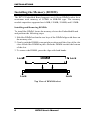
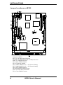
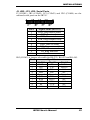
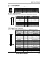
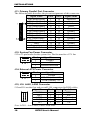
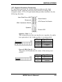
1
IB795
VIA Eden/C3 VIA Apollo
PN133T 5.25-inch SBC
USER’S MANUAL
Version 1.0B
Acknowledgments
Award is a registered trademark of Award Software International,
Inc.
PS/2 is a trademark of International Business Machines
Corporation.
Microsoft Windows is a registered trademark of Microsoft
Corporation.
Winbond is a registered trademark of Winbond Electronics
Corporation.
All other product names or trademarks are properties of their
respective owners.
ii
IB795 User’s Manual
Table of Contents
Introduction ..............................................................1
Product Description...........................................................1
Checklist...........................................................................2
Specifications....................................................................3
Board Dimensions.............................................................4
Installations ..............................................................5
Installing the Memory (DIMM) .........................................6
Setting the Jumpers...........................................................7
Connectors on IB795.......................................................12
Watchdog Timer Configuration.......................................24
BIOS Setup .............................................................25
Drivers Installation .................................................47
VIA 4 in 1 Drivers Installation ........................................48
VGA Drivers Installation ................................................53
LAN Drivers Installation.................................................56
Audio Drivers Installation ...............................................59
Appendix .................................................................60
A. I/O Port Address Map.................................................60
B. Interrupt Request Lines (IRQ).....................................61
C. STN Flat Panel Data Outputs......................................62
D. TFT Flat Panel Data Outputs ......................................63
E. About the digital I/O ...................................................65
IB795 User’s Manual
iii
This page was intentionally left blank.
iv
IB795 User’s Manual
INTRODUCTION
Introduction
Product Description
IB795 is a high-performance flexible embedded board based on the VIA
ProSavage TwisterT (PN133T) chipset. The chipset is based on an
innovative and scaleable architecture with proven reliability. It is a
two-chip set consisting of the VT8606 North Bridge Controller and
VT82C686B South Bridge Controller.
IB795 supports the VIA Eden/C3 processors that features Native x86
execution, Integrated full-speed 192KB L1/L2 cache, 100/133MHz
Front Side Bus, Advanced multimedia instruction set, and MMX™ &
3DNow!™
The VT8606 integrated graphics accelerator supports 8/16/32MB frame
buffer using the system memory, integrated 2-channel 110MHz LVDS
interface and digital port for NTSC/PAL TV encoder. One or two
Ethernets can be supported by the Realtek 8139C single chip Ethernet
controller. Additional key features include support for two USB ports,
AC-97 link for audio, hardware monitoring, and power management.
System memory is provided by one 168-pin DIMM socket that
accommodates SDRAM with a maximum capacity of 512MB. The
Award BIOS facilitates easy system configuration and peripheral setup.
Other advanced features include DiskOnChip flash disk support,
16-level watchdog timer, and IrDA interface.
DiskOnChip flash disks are storage devices that have no moving parts
and emulate FDD/HDD with Flash/RAM/ROM offering reliable
data/program storage and long life span. They are reliable and suitable
for industrial or other harsh environments characterized by motion,
shock, vibration, adverse temperature, dust and humidity. Other features
include faster data access, longer MTBF, lower power consumption, cost
effective for small capacity and small form factor.
IB795 User’s Manual
1
INTRODUCTION
Checklist
Your IB795 package should include the items listed below.
• The IB795 Embedded Board
• This User’s Manual
• 1 CD containing chipset drivers and flash memory utility
• Optional cables such as:
• 1 FDD Ribbon Cable
• 1 Audio Cable
• 2 IDE Ribbon Cables (40-pin & 44-pin)
• 1 COM Port Cable
• 1 Printer Port Cable
• 1 PS/2 Keyboard/Mouse Cable
• 1 VGA Cable
• IBLD cable bracket for dual Ethernet
• RJ-45 Cable
• Single USB Port Cable Bracket
2
IB795 User’s Manual
INTRODUCTION
Specifications
Processor
Supported
Chipset
BIOS
System Memory
I/O Chipset
I/O Features
Bus Master IDE
VGA
LCD Interface
TV Out
(Optional)
Audio
LAN
USB
Watchdog Timer
Hardware
Monitoring
DiskOnChip
Digital I/O
Expansion Slot
Power
Consumption
Form Factor
Dimensions
VIA Eden or C3 processors on board
100/133MHz Front Side Bus
VIA Apollo PN133T Chipset
North bridge: VT8606 (552-pin BGA package)
South bridge: VT82C686B (352-pin BGA package)
Award BIOS
Supports ACPI, DMI, PnP
1x DIMM socket supports up to 512MB capacity
PC100/PC133 supported
VT82C686B chipset
Keyboard controller built-in
1x FDD (up to 2.88MB, 3 Mode, LS120)
2x Parallel Port (EPP, ECP Port)
4x Serial Ports (3x RS232 and 1x RS232/422/485)
1x IrDA TX/RX Headers
2x IDE interfaces for up to 4 devices; supports PIO Mode
3/4 or UDMA/33/66/100 HDD, and ATAPI CD-ROM
VT8606 integrated graphics controller
8/16/32MB frame buffer with system memory
Integrated 2-channel 110MHz LVDS interface
Digital port for TV encoder
Supports 36 bit TTL LCD interface and 2 channel LVDS
VIA VT1621 TV Encoder
Composite and S-Video output
VT82C686B chipset built-in sound controller
With AC97 Codec
One or two Realtek RTL8139C Ethernet controllers
10Base-T / 100Base-TX protocol
2 ports (pin header)
16 levels (0, 2, 4, 6, … 30 sec.)
Built-in VT82C686B chipset
Monitors CPU/system temperature and voltages
Support M-Systems 2MB~288MB DiskOnChip flash disk
4 in, 4 out
One 32-bit PCI slot
One PC/104 expansion slot
+5V: 6A max. +12V: 750mA max.
5.25-inch SBC (Little Board)
203mm x 146mm (7.99” x 5.75”)
IB795 User’s Manual
3
INTRODUCTION
Board Dimensions
4
IB795 User’s Manual
INSTALLATIONS
Installations
This section provides information on how to use the jumpers and
connectors on the IB795 in order to set up a workable system. The topics
covered are:
Installing the Memory (DIMM) .........................................6
Setting the Jumpers...........................................................7
Connectors on IB795.......................................................12
IB795 User’s Manual
5
INSTALLATIONS
Installing the Memory (DIMM)
The IB795 Embedded Board supports one 168-pin DIMM socket for a
maximum total memory of 512MB in SDRAM type. The memory
module capacities supported are 64MB, 128MB, 256MB, and 512MB.
Installing and Removing DIMMs
To install the DIMM, locate the memory slot on the Embedded Board
and perform the following steps:
1. Hold the DIMM so that the two keys of the DIMM align with those on
the memory slot.
2. Gently push the DIMM in an upright position until the clips of the slot
close to hold the DIMM in place when the DIMM touches the bottom
of the slot.
3. To remove the DIMM, press the clips with both hands.
Lock
DIMM
Lock
Lock
Top View of DIMM Socket
6
Lock
IB795 User’s Manual
INSTALLATIONS
Setting the Jumpers
Jumpers are used on IB795 to select various settings and features
according to your needs and applications. Contact your supplier if you
have doubts about the best configuration for your needs. The following
lists the connectors on IB795 and their respective functions.
Jumper Locations on IB795................................................................ 8
SW1(3): CPU Bus Speed Selector ..................................................... 9
JP1, JP4, JP6: RS232/422/485 (COM2) Selection............................ 9
JPX2: TV Output Selection ................................................................ 9
JP2: LAN1 Enable/Disable............................................................... 10
JP3: LCD Power Setting ................................................................... 10
JP5: COM3/4 RS232 +5V / +12V Power Setting........................... 10
JP7: COM1/2 RS232 +5V / +12V Power Setting........................... 10
JP8: LAN2 Enable/Disable............................................................... 11
JP9: DiskOnChip Address Select ..................................................... 11
JP10: AT/ATX Power Selection ...................................................... 11
JP11: Clear CMOS Content .............................................................. 11
IB795 User’s Manual
7
INSTALLATIONS
Jumper Locations on IB795
Jumpers on IB795
SW1(3): CPU Bus Speed Selector
JP1, JP4, JP6: RS232/422/485 (COM2) Selection
JPX2: TV Output Selection
JP2: LAN1 Enable/Disable
JP3: LCD Power Setting
JP5: COM3/4 RS232 +5V / +12V Power Setting
JP7: COM1/2 RS232 +5V / +12V Power Setting
JP8: LAN2 Enable/Disable
JP9: DiskOnChip Address Select
JP10: AT/ATX Power Selection
JP11: Clear CMOS Content
8
IB795 User’s Manual
INSTALLATIONS
SW1(3): CPU Bus Speed Selector
Bus Speed
SW1(3)
Switch Setting
66MHz
off off on on
100MHz
off off off on
133MHz
off off off off
JP1, JP4, JP6: RS232/422/485 (COM2) Selection
COM1 is fixed for RS-232 use only.
COM2 is selectable for RS232, RS-422 and RS-485.
The following table describes the jumper settings for COM2 selection.
COM2
Function
Jumper
Setting
(pin closed)
RS-232
RS-422
RS-485
JP1:
3-5 & 4-6
JP1:
1-3 & 2-4
JP1:
1-3 & 2-4
JP4:
3-5 & 4-6
JP4:
1-3 & 2-4
JP4:
1-3 & 2-4
JP6:
1-2
JP6:
3-4
JP6:
5-6
JPX2: TV Output Selection
JPX2
Setting
TV Output
Short/Closed
TV Output
Open
LCD Output
IB795 User’s Manual
9
INSTALLATIONS
JP2: LAN1 Enable/Disable
JP2
Setting
LAN1
Short/Closed
Enabled
Open
Disabled
JP3: LCD Power Setting
JP3
Setting
Function
Pin 1-2
Short/Closed
3.3V
Pin 2-3
Short/Closed
5V
JP5: COM3/4 RS232 +5V / +12V Power Setting
Pin #
Signal Name
1
JP5
Signal Name
Pin #
+5V
+5V
2
3
Pin 9 (COM3)
Pin 9 (COM4)
4
5
+12V
+12V
6
COM3 Settings: Pin 1-3 short = +5V, Pin 3-5 short = +12V
COM4 Settings: Pin 2-4 short = +5V, Pin 4-6 short = +12V
JP7: COM1/2 RS232 +5V / +12V Power Setting
Pin #
Signal Name
1
JP7
Signal Name
Pin #
+5V
+5V
2
3
Pin 9 (COM1)
Pin 9 (COM2)
4
5
+12V
+12V
6
COM1 Settings: Pin 1-3 short = +5V, Pin 3-5 short = +12V
COM2 Settings: Pin 2-4 short = +5V, Pin 4-6 short = +12V
10
IB795 User’s Manual
INSTALLATIONS
JP8: LAN2 Enable/Disable
JP8
Setting
LAN2
Short/Closed
Enabled
Open
Disabled
JP9: DiskOnChip Address Select
JP9
Setting
Address
Pin 1-2
Short/Closed
D0000-D7FF
Pin 2-3
Short/Closed
D8000-DFFF
JP10: AT/ATX Power Selection
JP10
Setting
AT / ATX Power
Short/Closed
Select ATX Power
Open
Select AT Power
JP11: Clear CMOS Content
JP11
Setting
Function
Pin 1-2
Short/Closed
Normal Operation
Pin 2-3
Short/Closed
Clear CMOS Content
IB795 User’s Manual
11
INSTALLATIONS
Connectors on IB795
The connectors on IB795 allows you to connect external devices such as
keyboard, floppy disk drives, hard disk drives, printers, etc. The
following table lists the connectors on IB795 and their respective
functions.
Connector Locations on IB795......................................................... 13
J1: LCD Panel Connector ................................................................. 14
J2, JB2, JC2, JD2: Serial Ports......................................................... 15
J3, J9: 1st and 2nd Channel LVDS Connector (DF13-20)............. 16
J4: LCD Inverter Output................................................................... 16
J6: Secondary Parallel Port Connector............................................. 16
J7: TV-Out Connector....................................................................... 17
J8: VGA CRT Connector.................................................................. 17
J10: Floppy Drive Connector ........................................................... 17
J11: Primary Parallel Port Connector............................................... 18
J12: System Fan Power Connector................................................... 18
J14: External ATX Power Connector .............................................. 18
J15, J16: LAN1, LAN2 Connector................................................... 18
J17: System Function Connector...................................................... 19
J18: Digital I/O.................................................................................. 21
J20: CPU Fan Power Connector....................................................... 21
J21: USB Connector.......................................................................... 21
J22: Audio Connector ....................................................................... 21
J23: IrDA Connector......................................................................... 22
J24: External Keyboard Connector .................................................. 22
J25, J26: Primary and Secondary IDE Connectors ......................... 22
J27: PS/2 Keyboard/Mouse Connector............................................ 23
J28: CD-in Connector ....................................................................... 23
12
IB795 User’s Manual
INSTALLATIONS
Connector Locations on IB795
J1: LCD Panel Connector
J2, JB2, JC2, JD2: Serial Ports
J3: 1st Channel LVDS Connector (DF13-20)
J4: LCD Inverter Output
J6: Secondary Parallel Port Connector
J7: TV-Out Connector
J8: VGA CRT Connector
J9: 2nd Channel LVDS Connector (DF13-20)
J10: Floppy Drive Connector
J11: Primary Parallel Port Connector
J12: System Fan Power Connector
J14: External ATX Power Connector
J15, J16: LAN1, LAN2 Connector
J17: System Function Connector
J18: Digital I/O
J20: CPU Fan Power Connector
J21: USB Connector
J22: Audio Connector
J23: IrDA Connector
J24: External Keyboard Connector
J25, J26: Primary and Secondary IDE Connectors
J27: PS/2 Keyboard/Mouse Connector
J28: CD-in Connector
IB795 User’s Manual
13
INSTALLATIONS
J1: LCD Panel Connector
J1 is the TTL interface pin header for flat panel LCD displays. The
following shows the pin assignments of this connector.
Signal Name
+12V
Ground
5V/3.3V
ENAVEE
P0
P2
P4
P6
P8
P10
P12
P14
P16
P18
P20
P22
Ground
SHFCLK
MDE
Ground
Ground
DNAVDD
NC
P24
P26
P28
P30
P32
P34
14
Pin #
1
3
5
7
9
11
13
15
17
19
21
23
25
27
29
31
33
35
37
39
41
43
45
47
49
51
53
55
57
Pin #
2
4
6
8
10
12
14
16
18
20
22
24
26
28
30
32
34
36
38
40
42
44
46
48
50
52
54
56
58
IB795 User’s Manual
Signal Name
+12V
Ground
5V/3.3V
Ground
P1
P3
P5
P7
P9
P11
P13
P15
P17
P19
P21
P23
Ground
FLM
LP
ENABKL
NC
5V/3.3V
NC
P25
P27
P29
P31
P33
P35
INSTALLATIONS
J2, JB2, JC2, JD2: Serial Ports
J2 (COM1), JB2 (COM2), JC2 (COM3) and JD2 (COM4) are the
onboard serial ports on the IB795.
Pin #
1
2
3
4
5
6
7
8
9
10
Signal Name (RS-232)
DCD, Data carrier detect
RXD, Receive data
TXD, Transmit data
DTR, Data terminal ready
Ground
DSR, Data set ready
RTS, Request to send
CTS, Clear to send
RI, Ring indicator
No Connect.
JB2 (COM2) is jumper selectable for RS-232, RS-422 and RS-485.
Pin #
Signal Name
RS-232
R2-422
RS-485
1
DCD
TXDATA2
RX
TX+
DATA+
3
TX
RX+
NC
4
DTR
RXNC
5
Ground
Ground
Ground
6
DSR
RTSNC
7
RTS
RTS+
NC
8
CTS
CTS+
NC
9
RI
CTSNC
10
NC
NC
NC
IB795 User’s Manual
15
INSTALLATIONS
J3, J9: 1st and 2nd Channel LVDS Connector (DF13-20)
Signal Name
TX0Ground
TX15V/3.3V
NC
TX2Ground
TXC5V/3.3V
+12V
Pin #
2
4
6
8
10
12
14
16
18
20
Pin #
1
3
5
7
9
11
13
15
17
19
Signal Name
TX0+
Ground
TX1+
Ground
NC
TX2+
Ground
TXC+
ENABKL
+12V
J4: LCD Inverter Output
Pin #
1
2
3
4
5
Signal Name
+12V
Ground
ENVEE
NC
Vcc
J6: Secondary Parallel Port Connector
The following table describes the pin out assignments of this connector.
Signal Name
Line printer strobe
PD0, parallel data 0
PD1, parallel data 1
PD2, parallel data 2
PD3, parallel data 3
PD4, parallel data 4
PD5, parallel data 5
PD6, parallel data 6
PD7, parallel data 7
ACK, acknowledge
Busy
Paper empty
Select
16
Pin #
1
2
3
4
5
6
7
8
9
10
11
12
13
Pin #
14
15
16
17
18
19
20
21
22
23
24
25
N/A
IB795 User’s Manual
Signal Name
AutoFeed
Error
Initialize
Select
Ground
Ground
Ground
Ground
Ground
Ground
Ground
Ground
N/A
INSTALLATIONS
J7: TV-Out Connector
J7 is a 6-pin header for the optional TV-Out connector.
Signal Name
Comp
S-Y
S-C
Pin #
1
3
5
Pin #
2
4
6
Signal Name
Ground
Ground
Ground
J8: VGA CRT Connector
J8 is a 15-pin header for an external VGA CRT female connector.
Signal Name
Red
Green
Blue
N.C.
Ground
Ground
Ground
Ground
Pin
1
3
5
7
9
11
13
15
Pin
2
4
6
8
10
12
14
16
Signal Name
Vcc
Ground
N.C.
N.C.
H-Sync
V-Sync
N.C.
N.C.
J10: Floppy Drive Connector
J10 is a 34-pin header and will support up to 2.88MB floppy drives.
Signal Name
Ground
Ground
Ground
Ground
Ground
Ground
Ground
Ground
Ground
Ground
Ground
Ground
Ground
Ground
Ground
Ground
Ground
Pin #
1
3
5
7
9
11
13
15
17
19
21
23
25
27
29
31
33
IB795 User’s Manual
Pin #
2
4
6
8
10
12
14
16
18
20
22
24
26
28
30
32
34
Signal Name
RM/LC
No connect
No connect
Index
Motor enable 0
Drive select 1
Drive select 0
Motor enable 1
Direction
Step
Write data
Write gate
Track 00
Write protect
Read data
Side 1 select
Diskette change
17
INSTALLATIONS
J11: Primary Parallel Port Connector
The following table describes the pin out assignments of this connector.
Signal Name
Pin # Pin #
Signal Name
Line printer strobe
1
14
AutoFeed
PD0, parallel data 0
2
15
Error
PD1, parallel data 1
3
16
Initialize
PD2, parallel data 2
4
17
Select
PD3, parallel data 3
5
18
Ground
PD4, parallel data 4
6
19
Ground
PD5, parallel data 5
7
20
Ground
PD6, parallel data 6
8
21
Ground
PD7, parallel data 7
9
22
Ground
ACK, acknowledge
10
23
Ground
Busy
11
24
Ground
Paper empty
12
25
Ground
Select
13
N/A
N/A
J12: System Fan Power Connector
J12 is a 3-pin header for the system fan. The fan must be a 12V fan.
Pin #
Signal Name
1
Ground
2
+12V
3
Rotation detection
J14: External ATX Power Connector
Pin #
Signal Name
1
Ground
2
PS-ON (soft on/off)
3
5VSB (Standby +5V)
J15, J16: LAN1, LAN2 Connector
J15 and J16 are the first and second LAN connectors for RJ45 cables.
Signal Name Pin # Pin # Signal Name
LED1+
1
6
LED1RX+
2
7
RXLED23
8
Ground
LED2+
4
9
Ground
TX+
5
10
TXNote: LED 1: Active LED; LED2: Link LED
18
IB795 User’s Manual
INSTALLATIONS
J17: System Function Connector
J17 provides connectors for system indicators that provide light
indication of the computer activities and switches to change the
computer status. J17 is a 20-pin header that provides interfaces for the
following functions.
Hard Disk Drive LED
Reset Switch
Reserved
ATX Power On Switch
SMI / Hardware Switch
Speaker
Power LED
Speaker: Pins 1 - 4
This connector provides an interface to a speaker for audio
tone generation. An 8-ohm speaker is recommended.
Pin #
1
2
3
4
Signal Name
Speaker out
No connect
Ground
+5V
Power LED: Pins 11 - 13
The power LED indicates the status of the main power
switch.
Pin #
11
12
13
IB795 User’s Manual
Signal Name
Power LED
No connect
Ground
19
INSTALLATIONS
SMI/Hardware Switch: Pins 6 and 16
This connector supports the "Green Switch" on the control
panel, which, when pressed, will force the system into the
power-saving mode immediately.
Pin #
6
16
Signal Name
Sleep
Ground
ATX Power ON Switch: Pins 7 and 17
This 2-pin connector is an “ATX Power Supply On/Off
Switch” on the system that connects to the power switch on
the case. When pressed, the power switch will force the
system to power on. When pressed again, it will force the
system to power off.
Reset Switch: Pins 9 and 19
The reset switch allows the user to reset the system without
turning the main power switch off and then on again.
Orientation is not required when making a connection to
this header.
Hard Disk Drive LED Connector: Pins 10 and 20
This connector connects to the hard drive activity LED on
control panel. This LED will flash when the HDD is being
accessed.
Pin #
Signal Name
10
Ground
20
5V
20
IB795 User’s Manual
INSTALLATIONS
J18: Digital I/O Connector (4 in, 4 out)
This 12-pin Digital I/O connector supports TTL levels and is used to
control external devices requiring ON/OFF circuitry.
Signal Name
In0
In1
In2
In3
Ground
Out2
Pin #
1
2
3
4
5
6
Pin #
7
8
9
10
11
12
Signal Name
+5V
Out0
Ground
Out1
+12V
Out3
J20: CPU Fan Power Connector
J20 is a 3-pin header for the CPU fan power.
Pin #
1
2
3
Signal Name
Ground
+12V
Rotation detection
J21: USB Connector
J21 supports an external USB connector with two ports.
Pin #
1
5
2
6
3
7
4
8
Signal Name
Vcc
USBUSB+
Ground
J22: Audio Connector
J22, a 12-pin header connector, supports an optional external connector
supporting 3 sockets for Line Out, Line In and Mic functions. The
following table shows the pin assignments of this connector.
Signal Name
Line Out R
Ground
Line In R
Ground
Mic
Ground
Pin #
1
3
5
7
9
11
Pin #
2
4
6
8
10
12
IB795 User’s Manual
Signal Name
Line Out L
Ground
Line In L
Ground
BIAS
NC
21
INSTALLATIONS
J23: IrDA Connector
J23 is used for an optional IrDA connector for infrared wireless
communication.
Pin #
Signal Name
1
+5V
2
No connect
3
Ir RX
4
Ground
5
Ir TX
J24: External Keyboard Connector
J24 is a a 5-pin header for the external keyboard connector.
Pin #
Signal Name
1
+5V
2
KBCLK-OUT
3
KBCLK-IN
4
KBDAT-OUT
5
KBDAT-IN
6
Ground
J25, J26: Primary and Secondary IDE Connectors
J25: Primary IDE Connector
Signal Name
Pin #
Pin #
Signal Name
Reset IDE
1
2
Ground
Host data 7
3
4
Host data 8
Host data 6
5
6
Host data 9
Host data 5
7
8
Host data 10
Host data 4
9
10
Host data 11
Host data 3
11
12
Host data 12
Host data 2
13
14
Host data 13
Host data 1
15
16
Host data 14
Host data 0
17
18
Host data 15
Ground
19
20
Protect pin
DRQ0
21
22
Ground
Host IOW
23
24
Ground
Host IOR
25
26
Ground
IOCHRDY
27
28
Host ALE
DACK0
29
30
Ground
IRQ14
31
32
No connect
Address 1
33
34
No connect
Address 0
35
36
Address 2
Chip select 0
37
38
Chip select 1
Activity
39
40
Ground
22
IB795 User’s Manual
INSTALLATIONS
J26: Secondary IDE Connector
Signal Name
Pin #
Pin #
Reset IDE
Host data 7
Host data 6
Host data 5
Host data 4
Host data 3
Host data 2
Host data 1
Host data 0
Ground
DRQ0
Host IOW
Host IOR
IOCHRDY
DACK0
IRQ14
Address 1
Address 0
Chip select 0
Activity
Vcc
Ground
1
3
5
7
9
11
13
15
17
19
21
23
25
27
29
31
33
35
37
39
41
43
2
4
6
8
10
12
14
16
18
20
22
24
26
28
30
32
34
36
38
40
42
44
Signal Name
Ground
Host data 8
Host data 9
Host data 10
Host data 11
Host data 12
Host data 13
Host data 14
Host data 15
Key
Ground
Ground
Ground
Host ALE
Ground
No connect
No connect
Address 2
Chip select 1
Ground
Vcc
N.C.
J27: PS/2 Keyboard/Mouse Connector
J27, a 10-pin header connector, has functions for keyboard and mouse.
Signal Name
N.C.
KB clock
KB data
Vcc
Ground
Pin #
10
9
8
7
6
Pin #
5
4
3
2
1
Signal Name
N.C.
Mouse clock
Mouse data
Vcc
Ground
J28: CD-in Connector
J28 is the 4-pin CD-in connector.
Pin #
1
2
3
4
Signal Name
Right
Ground
Ground
Left
IB795 User’s Manual
23
INSTALLATIONS
Watchdog Timer Configuration
The function of the watchdog timer is to reset the system automatically
and is defined at I/O port 0443H. To enable the watchdog timer and
allow the system to reset, write I/O port 0443H. To disable the timer,
write I/O port 0441H for the system to stop the watchdog function. The
timer has a tolerance of 20% for its intervals.
The following describes how the timer should be programmed.
Enabling Watchdog:
MOV AX, 000FH (Choose the values from 0)
MOV DX, 0443H
OUT DX, AX
Disabling Watchdog
MOV AX, 00FH (Any value is fine.)
MOV
DX, 0441H
OUT DX, AX
WATCHDOG TIMER CONTROL TABLE
Level
1
2
3
4
5
6
7
8
24
Value
F
E
D
C
B
A
9
8
Time/sec
0
2
4
6
8
10
12
14
Level
9
10
11
12
13
14
15
16
Value
7
6
5
4
3
2
1
0
IB795 User’s Manual
Time/sec
16
18
20
22
24
26
28
30
BIOS SETUP
BIOS Setup
This chapter describes the different settings available in the Award BIOS
that comes with the Embedded Board. The topics covered in this chapter
are as follows:
BIOS Introduction............................................................................. 26
BIOS Setup........................................................................................ 26
Standard CMOS Setup...................................................................... 28
Advanced BIOS Features.................................................................. 31
Advanced Chipset Features .............................................................. 34
Integrated Peripherals........................................................................ 37
Power Management Setup ................................................................ 39
PNP/PCI Configurations................................................................... 42
PC Health Status................................................................................ 43
Frequency/Voltage Control .............................................................. 44
Load Fail-Safe Defaults .................................................................... 45
Load Setup Defaults.......................................................................... 45
Set Supervisor/User Password.......................................................... 45
Save & Exit Setup ............................................................................. 45
Exit Without Saving .......................................................................... 45
IB795 User’s Manual
25
BIOS SETUP
BIOS Introduction
The Award BIOS (Basic Input/Output System) installed in your
computer system’s ROM supports Intel Pentium II/III processors. The
BIOS provides critical low-level support for a standard device such as
disk drives, serial ports and parallel ports. It also adds virus and
password protection as well as special support for detailed fine-tuning of
the chipset controlling the entire system.
BIOS Setup
The Award BIOS provides a Setup utility program for specifying the
system configurations and settings. The BIOS ROM of the system stores
the Setup utility. When you turn on the computer, the Award BIOS is
immediately activated. Pressing the <Del> key immediately allows you
to enter the Setup utility. If you are a little bit late pressing the <Del>
key, POST (Power On Self Test) will continue with its test routines, thus
preventing you from invoking the Setup. If you still wish to enter Setup,
restart the system by pressing the ”Reset” button or simultaneously
pressing the <Ctrl>, <Alt> and <Delete> keys. You can also restart by
turning the system Off and back On again. The following message will
appear on the screen:
Press
<DEL>
to
Enter
Setup
In general, you press the arrow keys to highlight items, <Enter> to select,
the <PgUp> and <PgDn> keys to change entries, <F1> for help and
<Esc> to quit.
When you enter the Setup utility, the Main Menu screen will appear on
the screen. The Main Menu allows you to select from various setup
functions and exit choices.
26
IB795 User’s Manual
BIOS SETUP
Phoenix - AwardBIOS CMOS Setup Utility
Standard CMOS Features
Advanced BIOS Features
Advanced Chipset Features
Integrated Peripherals
Power Management Setup
PnP/PCI Configurations
PC Health Status
ESC : Quit
F10 : Save & Exit Setup
Time, Date, Hard
Frequency/Voltage Control
Load Fail-Safe Defaults
Load Optimized Defaults
Set Supervisor Password
Set User Password
Save & Exit Setup
Exit Without Saving
á â à ß : Select Item
Disk Type…
The section below the setup items of the Main Menu displays the control
keys for this menu. At the bottom of the Main Menu just below the
control keys section, there is another section which displays information
on the currently highlighted item in the list.
Note:
If the system cannot boot after making and saving system
changes with Setup, the Award BIOS supports an override to
the CMOS settings that resets your system to its default.
Warning: It is strongly recommended that you avoid making any
changes to the chipset defaults. These defaults have been
carefully chosen by both Award and your system
manufacturer to provide the absolute maximum performance
and reliability. Changing the defaults could cause the system
to become unstable and crash in some cases.
IB795 User’s Manual
27
BIOS SETUP
Standard CMOS Setup
“Standard CMOS Setup” choice allows you to record some basic
hardware configurations in your computer system and set the system
clock and error handling. If the board is already installed in a working
system, you will not need to select this option. You will need to run the
Standard CMOS option, however, if you change your system hardware
configurations, the onboard battery fails, or the configuration stored in
the CMOS memory was lost or damaged.
Phoenix - AwardBIOS CMOS Setup Utility
Standard CMOS Features
Date (mm:dd:yy)
Tue, Mar 26 2000
Time (hh:mm:ss)
00 : 00 : 00
Menu Level
Item Help
IDE Primary Master
IDE Primary Slave
IDE Secondary Master
IDE Secondary Slave
Press Enter 13020 MB
Press Enter None
Press Enter None
Press Enter None
Change the day, month,
Year and century
Drive A
Drive B
1.44M, 3.5 in.
None
Halt On
Select Display Device
All, But Keyboard
CRT + LCD
Base Memory
Extended Memory
Total Memory
640K
129024K
130048K
At the bottom of the menu are the control keys for use on this menu. If
you need any help in each item field, you can press the <F1> key. It will
display the relevant information to help you. The memory display at the
lower right-hand side of the menu is read-only. It will adjust
automatically according to the memory changed. The following
describes each item of this menu.
Date
The date format is:
Day :
Month :
Date :
Year :
Sun to Sat
1 to 12
1 to 31
1994 to 2079
To set the date, highlight the “Date” field and use the PageUp/
PageDown or +/- keys to set the current time.
28
IB795 User’s Manual
BIOS SETUP
Time
The time format is:
Hour :
Minute :
Second :
00 to 23
00 to 59
00 to 59
To set the time, highlight the “Time” field and use the <PgUp>/ <PgDn>
or +/- keys to set the current time.
IDE Primary HDDs / IDE Secondary HDDs
The onboard PCI IDE connectors provide Primary and Secondary
channels for connecting up to four IDE hard disks or other IDE devices.
Each channel can support up to two hard disks; the first is the “Master”
and the second is the “Slave”.
Press <Enter> to configure the hard disk. The selections include Auto,
Manual, and None. Select ‘Manual’ to define the drive information
manually. You will be asked to enter the following items.
CYLS :
HEAD :
PRECOMP :
LANDZ :
SECTOR :
Number of cylinders
Number of read/write heads
Write precompensation
Landing zone
Number of sectors
The Access Mode selections are as follows:
Auto
Normal (HD < 528MB)
Large (for MS-DOS only)
LBA (HD > 528MB and supports
Logical Block Addressing)
Drive A / Drive B
These fields identify the types of floppy disk drive A or drive B that has
been installed in the computer. The available specifications are:
360KB 1.2MB 720KB 1.44MB 2.88MB
5.25 in. 5.25 in. 3.5 in.
3.5 in.
3.5 in.
IB795 User’s Manual
29
BIOS SETUP
Halt On
This field determines whether or not the system will halt if an error is
detected during power up.
No errors
The system boot will not be halted for any error
that may be detected.
All errors
Whenever the BIOS detects a non-fatal error,
the system will stop and you will be prompted.
All, But Keyboard
The system boot will not be halted for a
keyboard error; it will stop for all other errors
All, But Diskette
The system boot will not be halted for a disk
error; it will stop for all other errors.
All, But Disk/Key
The system boot will not be halted for a keyboard or disk error; it will stop for all others.
Select Display Device
The options for this field are Auto, CRT, LCD, CRT+LCD, TV, and
CRT+TV.
30
IB795 User’s Manual
BIOS SETUP
Advanced BIOS Features
This section allows you to configure and improve your system and
allows you to set up some system features according to your preference.
Phoenix - AwardBIOS CMOS Setup Utility
Advanced BIOS Features
Virus Warning
CPU Internal Cache
External Cache
CPU L2 Cache ECC Checking
Processor Number Feature
Quick Power On Self Test
First Boot Device
Second Boot Device
Third Boot Device
Boot Other Device
Swap Floppy Drive
Boot Up Floppy Seek
Boot Up Numlock Status
Gate A20 Option
Typematic Rate Setting
Typematic Rate (chars/Sec)
Typematic Delay (Msec)
Security Option
OS Select For DRAM>64MB
Report no FDD for Win95
Video BIOS Shadow
C8000-CBFFF Shadow
CC000-CFFFF Shadow
D0000-D3FFF Shadow
D4000-D7FFF Shadow
D8000-DBFFF Shadow
DC000-DFFF Shadow
Small Logo (EPA) Show
Disabled
Enabled
Enabled
Enabled
Enabled
Enabled
Floppy
HDD-0
CDROM
Enabled
Disabled
Disabled
On
Fast
Disabled
6
250
Setup
Non-OS2
Yes
Enabled
: Disabled
: Disabled
: Disabled
: Disabled
: Disabled
: Disabled
: Enabled
ITEM HELP
Menu Level
Allows you choose
the VIRUS warning
feature for IDE Hard
Disk boot sector
protection. If this
function is enabled
and someone
attempt to write data
into this area, BIOS
will show a warning
message on screen
and alarm beep
Virus Warning
This item protects the boot sector and partition table of your hard disk
against accidental modifications. If an attempt is made, the BIOS will
halt the system and display a warning message. If this occurs, you can
either allow the operation to continue or run an anti-virus program to
locate and remove the problem.
CPU Internal Cache / External Cache
Cache memory is additional memory that is much faster than
conventional DRAM (system memory). CPUs from 486-type on up
contain internal cache memory, and most, but not all, modern PCs have
additional (external) cache memory. When the CPU requests data, the
system transfers the requested data from the main DRAM into cache
memory, for even faster access by the CPU. These items allow you to
enable (speed up memory access) or disable the cache function. By
default, these items are Enabled.
IB795 User’s Manual
31
BIOS SETUP
CPU L2 Cache ECC Checking
This field enables or disables the ECC (Error Correction Checking)
checking of the CPU level-2 cache. The default setting is Enabled.
Processor Number Feature
When enabled, this feature allows external systems to detect the
processor number/type of the CPU.
Quick Power On Self Test
When enabled, this field speeds up the Power On Self Test (POST) after
the system is turned on. If it is set to Enabled, BIOS will skip some
items.
First/Second/Third Boot Device
These fields determine the drive that the system searches first for an
operating system. The options available include Floppy, LS/ZIP,
HDD-0, SCSI, CDROM, HDD-1, HDD-2, HDD-3, LAN and Disable.
Boot Other Device
These fields allow the system to search for an operating system from
other devices other than the ones selected in the First/Second/Third Boot
Device.
Swap Floppy Drive
This item allows you to determine whether or not to enable Swap Floppy
Drive. When enabled, the BIOS swaps floppy drive assignments so that
Drive A becomes Drive B, and Drive B becomes Drive A. By default,
this field is set to Disabled.
Boot Up Floppy Seek
When enabled, the BIOS will seek whether or not the floppy drive
installed has 40 or 80 tracks. 360K type has 40 tracks while 760K, 1.2M
and 1.44M all have 80 tracks.
Boot Up NumLock Status
This allows you to activate the NumLock function after you power up
the system.
Gate A20 Option
This field allows you to select how Gate A20 is worked. Gate A20 is a
device used to address memory above 1 MB.
32
IB795 User’s Manual
BIOS SETUP
Typematic Rate Setting
When disabled, continually holding down a key on your keyboard will
generate only one instance. When enabled, you can set the two typematic
controls listed next. By default, this field is set to Disabled.
Typematic Rate (Chars/Sec)
When the typematic rate is enabled, the system registers repeated
keystrokes speeds. Settings are from 6 to 30 characters per second.
Typematic Delay (Msec)
When the typematic rate is enabled, this item allows you to set the time
interval for displaying the first and second characters. By default, this
item is set to 250msec.
Security Option
This field allows you to limit access to the System and Setup. The default
value is Setup. When you select System, the system prompts for the User
Password every time you boot up. When you select Setup, the system
always boots up and prompts for the Supervisor Password only when the
Setup utility is called up.
OS Select for DRAM > 64MB
This option allows the system to access greater than 64MB of DRAM
memory when used with OS/2 that depends on certain BIOS calls to
access memory. The default setting is Non-OS/2.
Report No FDD For WIN 95
If you are using Windows 95/98 without a floppy disk drive, select
Enabled to release IRQ6. If you set this feature to Disabled, the BIOS
will not report the missing floppy drive to Win95/98.
Video BIOS Shadow
This item allows you to change the Video BIOS location from ROM to
RAM. Video Shadow will increase the video speed.
C8000 - CBFFF Shadow/DC000 - DFFFF Shadow
Shadowing a ROM reduces the memory available between 640KB to
1024KB. These fields determine whether or not optional ROM will be
copied to RAM.
Small Logo (EPA) Show
This field enables the showing of the EPA logo located at the upper right
of the screen during boot up.
IB795 User’s Manual
33
BIOS SETUP
Advanced Chipset Features
This Setup menu controls the configuration of the chipset.
Phoenix - AwardBIOS CMOS Setup Utility
Advanced Chipset Features
DRAM Timing By SPD
Memory Hole
P2C/C2P Concurrency
System BIOS Cacheable
Video BIOS Cacheable
Frame Buffer Size
AGP Aperture Size
AGP-4X Mode
AGP Driving Control
Panel Type
Boot Device Select
Power Supply Type
OnChip USB
USB Keyboard Support
OnChip Sound
CPU to PCI Write Buffer
PCI Dynamic Bursting
PCI Master 0 WS Write
PCI Delay Transaction
PCI#2 Access #1 Retry
AGP Master 1 WS Write
AGP Master 1 WS Read
Enabled
Disabled
Enabled
Disabled
Disabled
8M
64M
Enabled
Auto
07
Both
AT
Enabled
Disabled
Auto
Enabled
Enabled
Enabled
Disabled
Enabled
Disabled
Disabled
ITEM HELP
Menu Level
DRAM Timing by SPD
This field enables or disables the DRAM Timing based on SPD.
Memory Hole
It is recommended to leave as disabled, although enabling 15M-16M can
help with sound issues.
P2C / C2P Concurrency
Set to Disabled for best performance. You may set this to Enabled if you
want any sort of system stability.
System BIOS Cacheable
The setting of Enabled allows caching of the system BIOS ROM at
F000h-FFFFFh, resulting in better system performance. However, if
any program writes to this memory area, a system error may result.
Video BIOS Cacheable
The Setting Enabled allows caching of the video BIOS ROM at
C0000h-F7FFFh, resulting in better video performance. However, if
any program writes to this memory area, a system error may result.
34
IB795 User’s Manual
BIOS SETUP
Frame Buffer Size
The default setting of the frame buffer size is 8M.
AGP Aperture Size
The field sets aperture size of the graphics. The aperture is a portion of
the PCI memory address range dedicated for graphics memory address
space. Host cycles that hit the aperture range are forwarded to the AGP
without any translation. The default setting is 64M.
AGP-4X Mode
The field enables or disables the AGP-4X mode of the integrated VGA
function.
AGP Driving Control
This BIOS function allows you to adjust the control of the AGP driving
force. It is set to Auto by default.
Panel Type
This field sets the panel type that is supported by the system. Below are
the selections for the different panel types:
Panel Type 0 640x480
18bit
TFT
1 800x600
18bit
TFT
2 1024x768
36bit
TFT
3 1280x1024
36bit
TFT
4 640x480
16bit
DSTN
5 800x600
16bit
DSTN
6 1024x768
16bit
DSTN
7 1024x768
18bit
1CH LVDS
8 640x480
18bit
TFT
9 800x600
18bit
TFT
A 1024x768
18bit
TFT
B 1280x1024
18bit
TFT
C 1400x1050
36bit
2CH LVDS
D 800x600
16bit
DSTN
E 1024x768
16bit
DSTN
F 1280x1024
16bit
DSTN
OnChip USB
The default setting is Enabled to enable the USB function on board.
Power Supply Type
Select AT or ATX depending on the type of power supply that is used.
IB795 User’s Manual
35
BIOS SETUP
OnChip Keyboard Support
Enable this if you are using a USB keyboard.
OnChip Sound
This field can be set as Auto or disabled.
CPU to PCI Write Buffer
This controls the CPU write buffer to the PCI bus. If this buffer is
disabled, the CPU writes directly to the PCI bus. The default setting is
Enabled.
PCI Dynamic Bursting
This option controls the PCI write buffer. If this is enabled, then every
write transaction on the PCI bus goes straight to the write buffer. Burst
transactions are then sent on their way as soon as there are enough to
send in a single burst.
PCI Master 0 WS Write
This function determines whether there's a delay before any writes to the
PCI bus. If this is enabled, then writes to the PCI bus are executed
immediately (with zero wait states), as soon as the PCI bus is ready to
receive data. But if it is disabled, then every write transaction to the PCI
bus is delayed by one wait state. It's recommended to enable this for
faster PCI performance.
PCI Delay Transaction
The chipset has an embedded 32-bit posted write buffer to support delay
transactions cycles. Select Enabled to support compliance with PCI
specification version 2.1.
PCI#2 Access #1 Retry
This BIOS feature is linked to the CPU to PCI Write Buffer. Normally,
the CPU to PCI Write Buffer is enabled. All writes to the PCI bus are, as
such, immediately written into the buffer, instead of the PCI bus. This
frees up the CPU from waiting till the PCI bus is free. The data are then
written to the PCI bus when the next PCI bus cycle starts.
AGP Master 1 WS Write/Read
When enabled a single wait state is used when writing/reading to the
AGP bus. When disabled a 2 wait state is used. For optimal performance
set this to enabled. For improved stability set it to disabled.
36
IB795 User’s Manual
BIOS SETUP
Integrated Peripherals
Phoenix - AwardBIOS CMOS Setup Utility
Integrated Peripherals
On-Chip IDE Channel 0
On-Chip IDE Channel 1
IDE Prefetch Mode
IDE Primary Master PIO
IDE Primary Slave PIO
IDE Secondary Master PIO
IDE Secondary Slave PIO
IDE Primary Master UDMA
IDE Primary Slave UDMA
IDE Secondary Master UDMA
IDE Secondary Slave UDMA
Init Display First
IDE HDD Block Mode
Onboard FDD Controller
Onboard Serial Port 1
Onboard Serial Port 2
UART 2 Mode
Onboard Parallel Port
Onboard Parallel Mode
ECP Mode Use DMA
Parallel Port EPP Type
Onboard Serial Port 3
Serial Port 3 Use IRQ
Onboard Serial Port 4
Serial Port 4 Use IRQ
Onboard Parallel Port 2
Chip Select Pin
Onboard Legacy Audio
Enabled
Enabled
Enabled
Auto
Auto
Auto
Auto
Auto
Auto
Auto
Auto
PCI Slot
Enabled
Enabled
3F8/IRQ4
2F8/IRQ3
Standard
378/IRQ7
Normal
3
EPP 1.9
3E8H
IRQ10
2E8H
IRQ11
Disabled
Disabled
Disabled
ITEM HELP
Menu Level
OnChip IDE Channel 0 / 1
The integrated peripheral controller contains an IDE interface with
support for two IDE channels. Select Enabled to activate each channel
separately.
IDE Prefetch Mode
These field enables/disables the prefetch buffers in the PCI IDE
controller. The prefetch buffers are used as a temporary storage place as
data is transferred from one location to another.
IDE Primary/Secondary Master/Slave PIO
These fields allow your system hard disk controller to work faster.
Rather than have the BIOS issue a series of commands that transfer to or
from the disk drive, PIO (Programmed Input/Output) allows the BIOS to
communicate with the controller and CPU directly.
The system supports five modes, numbered from 0 (default) to 4, which
primarily differ in timing. When Auto is selected, the BIOS will select
the best available mode.
IB795 User’s Manual
37
BIOS SETUP
IDE Primary/Secondary Master/Slave UDMA
These fields allow your system to improve disk I/O throughput to
33Mb/sec with the Ultra DMA/33 feature. The options are Auto and
Disabled.
Init Display First
This field allows the system to initialize first the VGA card on chip or
the display on the PCI Slot. By default, the PCI Slot VGA is initialized
first.
IDE HDD Block Mode
This field allows your hard disk controller to use the fast block mode to
transfer data to and from your hard disk drive.
Onboard FDD Controller
Select Enabled if your system has a floppy disk controller installed on
the Embedded Board and you wish to use it. If you install an add-in FDC
or the system has no floppy drive, select Disabled in this field. This
option allows you to select the onboard FDD port.
Onboard Serial/Parallel Port
These fields allow you to select the onboard serial and parallel ports and
their addresses. The default values for these ports are:
Serial Port 1
3F8/IRQ4
Serial Port 2
2F8/IRQ3
Serial Port 3
3E8H/IRQ10
Serial Port 4
2E8H/IRQ11
Parallel Port
378H/IRQ7
UART 2 Mode
This item allows you to determine which Infra Red (IR) function of
onboard I/O chip. The options are Standard, IrDA, and ASKIR.
Parallel Port Mode
This field allows you to determine parallel port mode function.
SPP
Standard Printer Port
EPP
Enhanced Parallel Port
ECP
Extended Capabilities Port
Onboard Legacy Audio
Enable or disable the on board legacy audio with this option. If enabled,
some audio options will appear.
38
IB795 User’s Manual
BIOS SETUP
Power Management Setup
The Power Management Setup allows you to save energy of your system
effectively.
Phoenix - AwardBIOS CMOS Setup Utility
Power Management Setup
ACPI Function
Power Management
PM Control by APM
Video Off Option
Video Off Method
Modem Use IRQ
Soft-Off by PWRBTN
Thermal Duty Cycle
Wake Up Events
Disabled
Press Enter
Yes
Suspend -> Off
V/H Sync + Blank
3
Instant-Off
Disabled
Press Enter
ITEM HELP
Menu Level
Phoenix - AwardBIOS CMOS Setup Utility
Power Management Setup
Power Management
User Define
HDd Power Down
Doze Mode
Suspend Mode
Disabled
Disabled
Disabled
ITEM HELP
Menu Level
Phoenix - AwardBIOS CMOS Setup Utility
IRQ/Event Activity Detect
VGA
OFF
LPT & COM
HDD & FDD
PCI Master
PowerOn by PCI Card
Modem Ring Resume
RTC Alarm Resume
IRQs Activity Monitoring
LPT / COM
ON
OFF
Disabled
Disabled
Disabled
Press Enter
ITEM HELP
Menu Level
Phoenix - AwardBIOS CMOS Setup Utility
IRQs Activity Monitoring
IRQ3
IRQ4
IRQ5
IRQ6
IRQ7
IRQ8
IRQ8
IRQ10
IRQ11
IRQ12
IRQ13
IRQ14
IRQ15
Disabled
Enabled
Enabled
Enabled
Enabled
Disabled
Disabled
Disabled
Disabled
Enabled
Enabled
Enabled
Disabled
IB795 User’s Manual
ITEM HELP
Menu Level
39
BIOS SETUP
ACPI Function
Use this option to enable or disable the ACPI function
Power Management
When you press Enter while selecting this field, the menu for Power
Management appears. The following are the fields in this menu.
Power Management
This field allows you to select the type of power saving management
modes. There are four selections for Power Management.
Min. Power Saving
Minimum power management
Max. Power Saving
Maximum power management.
User Define
Each of the ranges is from 1 min. to 1hr.
(Default)
Except for HDD Power Down which
ranges from 1 min. to 15 min.
Under this option, you can also configure other features such HDD
Power Down, Doze Mode and Suspend Mode.
HDD Power Down
After the selected period of drive inactivity, the hard disk drive
powers down while all other devices remain active. Control of this
mode is independent of the Power Management mode selected
previously.
Doze Mode
After the selected period of system inactivity, the CPU clock runs at
slower speed while all other devices still operate at full speed.
Suspend Mode
This option decides when to shutdown video for power saving. You
can select it as always on or turn off video when system enters
suspend mode.
PM Control by APM
If Advanced Power Management (APM) is installed on your system,
selecting Yes gives better power savings.
Video Off Option
This option decides when to shutdown video for power saving. You can
select it as always on or turn off video when system enters suspend
mode.
40
IB795 User’s Manual
BIOS SETUP
Video Off Method
This field defines the Video Off features. There are three options.
V/H SYNC + Blank
Default setting, blank the screen and turn
off vertical and horizontal scanning.
DPMS
Allows the BIOS to control the video
display card if it supports the DPMS
feature.
Blank Screen
This option only writes blanks to the video
buffer.
Modem Use IRQ
This field sets the IRQ used by the Modem. By default, the setting is 3.
Soft-Off by PWRBTN
This field defines the power-off mode when using an ATX power
supply. The Instant Off mode allows powering off immediately upon
pressing the power button. In the Delay 4 Sec mode, the system powers
off when the power button is pressed for more than four seconds or
enters the suspend mode when pressed for less than 4 seconds. The
default value is Instant Off.
Thermal Duty Cycle
This field enables or disables the thermal duty cycle.
Wake Up Events
The HDD, FDD, COM, LPT Ports, and PCI PIRQ are I/O events which
can prevent the system from entering a power saving mode or can
awaken the system from such a mode. When an I/O device wants to gain
the attention of the operating system, it signals this by causing an IRQ to
occur. When the operating system is ready to respond to the request, it
interrupts itself and performs the service.
IB795 User’s Manual
41
BIOS SETUP
PNP/PCI Configurations
This option configures the PCI bus system. All PCI bus systems on the
system use INT#, thus all installed PCI cards must be set to this value.
Phoenix - AwardBIOS CMOS Setup Utility
PnP/PCI Configurations
PNP OS Install
No
Reset Configuration Data
Disabled
Menu Level
ITEM HELP
Resources Controlled By
IRQ Resources
DMA Resources
Manual
Press Enter
Press Enter
PCI/VGA Palette Snoop
Assign IRQ for VGA
Assign IRQ for USB
Disabled
Enabled
Enabled
Default is Disabled.
Select Enabled to reset
Extended System
Configuration Data
(ESCD) when you exit
Setup if you have
installed a new add-on
and the system
reconfiguration has
caused such a serious
conflict that the OS
cannot boot
PNP OS Install
Enable the PNP OS Install option if it is supported by the operating
system installed. The default value is No.
Reset Configuration Data
This field allows you to determine whether to reset the configuration
data or not. The default value is Disabled.
Resources Controlled by
This PnP BIOS can configure all of the boot and compatible devices
automatically with the use of a use a PnP operating system such as
Windows 95.
PCI/VGA Palette Snoop
Some non-standard VGA display cards may not show colors properly.
This field allows you to set whether or not MPEG ISA/VESA VGA
cards can work with PCI/VGA. When this field is enabled, a PCI/VGA
can work with an MPEG ISA/VESA VGA card. When this field is
disabled, a PCI/VGA cannot work with an MPEG ISA/VESA card.
Assign IRQ for VGA/USB
By default, this fields are Enabled.
42
IB795 User’s Manual
BIOS SETUP
PC Health Status
This section shows the parameters in determining the PC Health Status.
These parameters include temperatures, fan speeds and voltages.
Phoenix - AwardBIOS CMOS Setup Utility
PC Health Status
CPU Warning Temperature
Current CPU Temp.
Current System Temp.
CPU Fan Speed (FAN1)
System Fan Speed (FAN2)
Vcore (V)
2.5V
3.3(V)
5(V)
12(V)
Disabled
34°C/95°F
28°C/82°F
4166 RPM
0 RPM
1.45V
2.47V
3.34V
5.05V
12.09V
ITEM HELP
CPU Warning Temperature
This field sets the temperature threshold that when reached, the system
would give an audible warning.
Temperatures/Fan Speeds/Voltages
These fields are the parameters of the hardware monitoring function
feature of the Embedded Board. The values are read-only values as
monitored by the system and show the PC health status.
IB795 User’s Manual
43
BIOS SETUP
Frequency/Voltage Control
This section shows the user how to configure the processor frequency.
Phoenix - AwardBIOS CMOS Setup Utility
Frequency/Voltage Control
Auto Detect DIMM/PCI Clk
Disabled
Spread Spectrum
Host CPU/PCI Clock
Disabled
Default
ITEM HELP
Menu Level
Auto Detect DIMM/PCI Clk
This field enables or disables the auto detection of the DIMM/PCI clock.
The default setting is Disabled.
Spread Spectrum
This field sets the value of the spread spectrum. The default setting is
Disabled. This field is for CE testing use only.
Host CPU/PCI Clock
The Host CPU/PCI Clock has a default setting of Default which
automatically detects the systems host CPU clock and PCI clock. You
can also use this parameter to overclock your system. However, it is
important to note that overclocking the system/CPU can cause your
system to become unstable or crash.
44
IB795 User’s Manual
BIOS SETUP
Load Fail-Safe Defaults
This option allows you to load the troubleshooting default values
permanently stored in the BIOS ROM. These default settings are
non-optimal and disable all high-performance features.
Load Setup Defaults
This option allows you to load the default values to your system
configuration. These default settings are optimal and enable all high
performance features.
Set Supervisor/User Password
These two options set the system password. Supervisor Password sets a
password that will be used to protect the system and Setup utility. User
Password sets a password that will be used exclusively on the system. To
specify a password, highlight the type you want and press <Enter>. The
Enter Password: message prompts on the screen. Type the password, up
to eight characters in length, and press <Enter>. The system confirms
your password by asking you to type it again. After setting a password,
the screen automatically returns to the main screen.
To disable a password, just press the <Enter> key when you are
prompted to enter the password. A message will confirm the password to
be disabled. Once the password is disabled, the system will boot and you
can enter Setup freely.
Save & Exit Setup
This option allows you to determine whether or not to accept the
modifications. If you type “Y”, you will quit the setup utility and save all
changes into the CMOS memory. If you type “N”, you will return to
Setup utility.
Exit Without Saving
Select this option to exit the Setup utility without saving the changes you
have made in this session. Typing “Y” will quit the Setup utility without
saving the modifications. Typing “N” will return you to Setup utility.
IB795 User’s Manual
45
BIOS SETUP
This page is intentionally left blank.
46
IB795 User’s Manual
APPENDIX
Drivers Installation
This section describes the installation procedures for software and
drivers under the Windows 98, Windows NT 4.0 and Windows 2000.
The software and drivers are included with the Embedded Board. If you
find the items missing, please contact the vendor where you made the
purchase. The contents of this section include the following:
VIA 4 in 1 Drivers Installation ........................................48
VGA Drivers Installation ................................................53
LAN Drivers Installation.................................................56
Sound Drivers Installation...............................................59
IB795 User’s Manual
47
APPENDIX
VIA 4 in 1 Drivers Installation
Before installing the drivers for VGA, LAN and Audio, install the VIA 4
in 1 drivers first. Follow the instructions below to complete the
installation.
1. Insert the CD that comes with the Embedded Board and the screen
below would appear. Click VIA Chipsets on the left side.
2. Click VIA 4 IN 1 Drivers.
48
IB795 User’s Manual
APPENDIX
3. When the Welcome screen appears, click Next.
4. Click Next to agree with the license agreement statement and to
continue.
IB795 User’s Manual
49
APPENDIX
5. Select the Setup Mode and click Next to continue.
6. Click Next to install the drivers listed.
50
IB795 User’s Manual
APPENDIX
7. Click Next to install the VIA ATAPI Vendor Support Driver.
8. Click Next to enable DMA Mode.
IB795 User’s Manual
51
APPENDIX
9. Click Next to install the VIA AGP VxD in Turbo mode.
10. Click Finish to restart the computer and for changes to take effect.
52
IB795 User’s Manual
APPENDIX
VGA Drivers Installation
After installing the VIA 4 in 1 drivers, you may now install the VIA
8606 VGA Driver. Follow the steps below to proceed with the
installation.
NOTE: Before installing the VGA drivers on Windows NT 4.0, you
need to install Service Pack 3 or above.
1. Insert the CD that comes with the Embedded Board and the screen
below would appear. Click VIA Chipsets on the left side.
2. Click VIA 8606 VGA Driver.
IB795 User’s Manual
53
APPENDIX
3. The welcome screen of the Twister Driver Setup will appear. Click
Next to continue.
4. When the Start Copying Files screen appears, click Next to start
copying the program files.
54
IB795 User’s Manual
APPENDIX
5. After file copying is done, the VGA driver installation is now
completed. Click Finish to restart the computer and for changes to take
effect.
IB795 User’s Manual
55
APPENDIX
LAN Drivers Installation
Follow the steps below to proceed with the LAN drivers installation.
1. In your Windows operating system, click Start à Settings à Control
Panel à System Properties.
56
IB795 User’s Manual
APPENDIX
2. Under System Properties, click on the Device Manager tab. Double
click on Realtek 8129 PCI Fast Ethernet. Click the Driver tab as shown.
Now click the Update Driver button.
3. When the Update Device Drivers Wizard appears, click Next to
continue.
IB795 User’s Manual
57
APPENDIX
4. Click Next to “Search for a better driver than the one your device is
using now. (Recommended”.
5. Click “Specify a location” and click Next to continue.
58
IB795 User’s Manual
APPENDIX
Audio Drivers Installation
NOTE: Please install the VGA drivers before proceeding with the
audio drivers installation .
Follow the steps below to proceed with the audio drivers installation.
1. Insert the CD that comes with the Embedded Board. Click on VIA
Chipsets on the left and then click VIA AC’97 Codec Audio Controller
Driver.
2. Under the Welcome screen, click Next to agree with the license
agreement statement and to continue.
IB795 User’s Manual
59
APPENDIX
Appendix
A. I/O Port Address Map
Each peripheral device in the system is assigned a set of I/O port
addresses, which also becomes the identity of the device. The following
table lists the I/O port addresses used.
Address
000h - 01Fh
020h - 03Fh
040h - 05Fh
060h - 06Fh
070h - 07Fh
080h - 09Fh
0A0h - 0BFh
0C0h - 0DFh
0F0h
0F1h
1F0h - 1F7h
278 - 27F
2F8h - 2FFh
2B0 - 2DF
378h - 3FFh
360 - 36F
3B0 - 3BF
3C0 - 3CF
3D0 - 3DF
3F0h - 3F7h
3F8h - 3FFh
60
Device Description
DMA Controller #1
Interrupt Controller #1
Timer
Keyboard Controller
Real Time Clock, NMI
DMA Page Register
Interrupt Controller #2
DMA Controller #2
Clear Math Coprocessor Busy Signal
Reset Math Coprocessor
IDE Interface
Parallel Port #2(LPT2)
Serial Port #2(COM2)
Graphics adapter Controller
Parallel Port #1(LPT1)
Network Ports
Monochrome & Printer adapter
EGA adapter
CGA adapter
Floppy Disk Controller
Serial Port #1(COM1)
IB795 User’s Manual
APPENDIX
B. Interrupt Request Lines (IRQ)
Peripheral devices use interrupt request lines to notify CPU for the
service required. The following table shows the IRQ used by the devices
on board.
Level
IRQ0
IRQ1
IRQ2
IRQ3
IRQ4
IRQ5
IRQ6
IRQ7
IRQ8
IRQ9
IRQ10
IRQ11
IRQ12
IRQ13
IRQ14
IRQ15
Function
System Timer Output
Keyboard
Interrupt Cascade
Serial Port #2
Serial Port #1
Reserved
Floppy Disk Controller
Parallel Port #1
Real Time Clock
Reserved
Serial Port 3
Serial Port 4
PS/2 Mouse
80287
Primary IDE
Secondary IDE
IB795 User’s Manual
61
APPENDIX
C. STN Flat Panel Data Outputs
Pin
FPD0
FPD1
FPD2
FPD3
FPD4
FPD5
FPD6
FPD7
FPD8
FPD9
FPD10
FPD11
FPD12
FPD13
FPD14
FPD15
FPD16
FPD17
FPD18
FPD19
FPD20
FPD21
FPD22
FPD23
FPD24
FPD25
FPD26
FPD27
FPD28
FPD29
FPD30
FPD31
FPD32
FPD33
FPD34
FPD35
62
STN8
R0
G0
B0
R1
G1
B1
R2
G2
STN16
R0
G0
B0
R1
G1
B1
R2
G2
B2
R3
G3
B3
R4
G4
B4
R5
STN24
R0
G0
B0
R1
G1
B1
R2
G2
B2
R3
G3
B3
R4
G4
B4
R5
G5
B5
R6
G6
B6
R7
G7
B7
DSTN8
LR0
DSNT16
LR0
LG0
LG0
DSTN24
LR0
LR3
LG0
LB0
LB0
LB0
LR1
LR1
LG1
LR1
LG3
LG1
LB1
LB1
LR2
LR2
LB3
LG2
LG2
UR0
UR0
UG0
UG0
UR0
UR3
UG0
UB0
UB0
UB0
UR1
UR1
UR1
UG3
UG1
UG1
UB1
UR2
UB1
UB3
UR2
UG2
UG2
IB795 User’s Manual
DSTN16
LB1
LB0
UB1
UB0
LG2
LG1
LG0
UG2
UG1
UG0
LR2
LR1
LR0
UR2
UR1
UR0
DSTN24
LB3
LB2
LB1
LB0
UB3
UB2
UB1
UB0
LG3
LG2
LG1
LG0
UG3
UG2
UG1
UG0
LR3
LR2
LR1
LR0
UR3
UR2
UR1
UR0
APPENDIX
D. TFT Flat Panel Data Outputs
Pin
FPD0
FPD1
FPD2
FPD3
FPD4
FPD5
FPD6
FPD7
FPD8
FPD9
FPD10
FPD11
FPD12
FPD13
FPD14
FPD15
FPD16
FPD17
FPD18
FPD19
FPD20
FPD21
FPD22
FPD23
FPD24
FPD25
FPD26
FPD27
FPD28
FPD29
FPD30
FPD31
FPD32
FPD33
FPD34
FPD35
TFT9
TFT2x9
TFT12
TFT2x12
TFT15
R0
R0
R0
R1
R2
R00
R10
R01
R11
R02
R12
R1
R2
R3
R00
R10
R01
R11
R02
R12
R03
R13
R1
R2
R3
R4
G0
G0
G0
G1
G2
G00
G10
G01
G11
G02
G12
G1
G2
G3
G00
G10
G01
G11
G02
G12
G03
G13
G1
G2
G3
G4
B0
B0
B0
B1
B2
B00
B10
B01
B11
B02
B12
B1
B2
B3
B00
B10
B01
B11
B02
B12
B03
B13
B1
B2
B3
B4
TFT2x15 TFT18
R00
R10
R01
R11
R02
R12
R03
R13
R04
R14
G00
G10
G01
G11
G02
G12
G03
G13
G04
G14
B00
B10
B01
B11
B02
B12
B03
B13
B04
B14
IB795 User’s Manual
B0
B1
B2
B3
B4
B5
G0
G1
G2
G3
G4
G5
R0
R1
R2
R3
R4
R5
TFT2x18
R00
R10
R01
R11
R02
R12
R03
R13
R04
R14
R05
R15
G00
G10
G01
G11
G02
G12
G03
G13
G04
G14
G05
G15
B00
B10
B01
B11
B02
B12
B03
B13
B04
B14
B05
B15
TFT24
R2
R0
R3
R4
R5
R1
R6
R7
G2
G0
R3
G4
G5
G1
G6
G7
B2
B0
B3
B4
B5
B1
B6
B7
63
APPENDIX
E. About the Digital I/O
J18: Digital I/O Connector (4 in, 4 out)
This 12-pin Digital I/O connector supports TTL levels and is used to
control external devices requiring ON/OFF circuitry.
Signal Name
In0
In1
In2
In3
Ground
Out2
Pin #
1
2
3
4
5
6
Pin #
7
8
9
10
11
12
Signal Name
+5V
Out0
Ground
Out1
+12V
Out3
SPECIFICATIONS:
Digital Input
Input channels: 4 bits
Input Voltage:
High: 2.0V (min)
Low: 0.8V (max)
Input Load:
High: 0.05mA max at 2.7V
Low: 0.4mA max at 0.5V
Register Address: 240H (Read)
Register Format: BIT: D3 D2 D1 D0
Value: IN3 IN2 IN1 IN0
Note: The input signal must be TTL compatible.
Digital Output
Output channels: 4 bits
Output voltage: High: Source -0.4mA at 2.4V min
Low: Sink 8mA at 0.5V max
Register Address: 240H (Write)
Register Format: BIT: D3 D2 D1 D0
Value: OUT3 OUT2 OUT1 OUT0
64
IB795 User’s Manual