1
GP-6W
Green Power Lab
User’s Manual
GP-6W
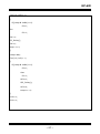
Content
1.
2.
3.
4.
5.
6.
7.
Green Power Introduction ………… 2
GP-6W Overview …………………… 3
Introduction for each unit ………… 5
The Testing way of MPPT ………… 24
Specification & Caution ………… 39
Experiment Content ……………
40
Standard & Optional Accessories 42
–3–
GP-6W
1. Green Power Introduction
1. The Earth's energy has been over-exploitation. We can not take anything just
like before. One day, when energy depletion of the earth, we will face a crisis
of survival.
So, we are looking for efficient and renewable energy andnd formed a global
trend of green renewable energy worldwidely.
2. Moreover, green renewable energy has become popular in the world. Many
countries also set this topic as a major industrial goal. We are starting with
theory and practice to create a complementary experimental platform which
makes everyone can join trend.
3. The GP-6W is the green energy renewable energy experimental platform. It
applicate solar energy which is the most representative. It should be the best
base knowledge for the academic education students. From this, we can
create more and wider application of technology.
–4–
GP-6W
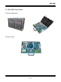
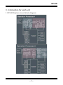
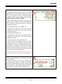
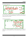
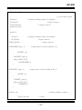
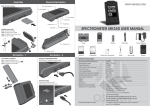
2. GP-6W Overview
Product appearance
Product inside
–5–
GP-6W
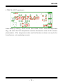
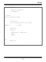
1. The GP-6W is a entry for the solar energy conversion platform. In order to allow
users to understand the "Maximum Power Point Tracking"(MPPT), we added
the single-chip feature that allows users to make changes for the "MPPT
algorithm, " Thus, a better understanding of the recycling of green energy.
2. Use of solar panels received the voltage and current to understand the features
of I / V, V / P and the curve with MPP and convert them into other applications.
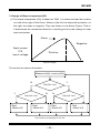
3. GP-6W solar system block diagram.
Solar Power
Storage device
(Battery)
DC/D C
LOAD
Wind Power
DC/AC
PWM
CONTROL
Detect Voltage
Detect Voltage
and Current
MCU
4. Features of GP-6W:
1. Application of MPPT algorithm.
2. LCD shows the input/output voltage, current and power value.
3. DC to DC converter module for learning of module transduction.
4. DC to AC inverter module convert output experiment.
5. Able to use MPU for power adjust control system. Use C or Assembly language
which make the teaching easier.
6. Learn the regeneration use of solar power through the charging module.
7. Learn the regeneration use of solar power through load module. Ex, LED
shining.
8. Based on open design. User can change the operating procedure during the
experiment.
–6–
GP-6W
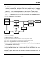
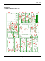
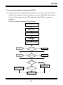
3. Introduction for each unit
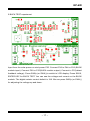
1.GP-6W System circuit block diagram
–7–
GP-6W
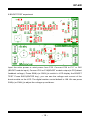
2.Platform
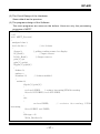
There are 15 areas on the GP-6W.
2
3
4
5
6
7
1
8
9
10
10
11
12
13
14
15
–8–
GP-6W
1.GREEN POWER LABModel name
1
GP-6W
2.LED19
DC power ON\OFF indicator. ON is red. Use
the SW6 for DC in control switch.
Or by other power supply, eg, USB, the LED
will light as well.
3.ADAPTER POWER IN power circuit
P22 for the DC input DC 9V ~ 12V (MAX),
It uses the step down IC which provide the
stable voltage source +3.3V for system
normal use, and via the step up IC to increase
+3.3V to +5V for linear circuit use.
4.SOLAR POWER
The solar input detective circuit. It will light
LED11~LED14 by the voltage up or down.
5.WIND POWER
Wind input detective circuit. It will light
LED15~LED18 by the voltage up or down.
There are 2 inputs, one is rectified which is
point P41, the other is un-rectified which is
point P40.
–9–
2
3
4
5
GP-6W
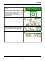
6.USB TO RS-232
The PC USB directly communicate with the
platform.
We can down load the driver from
http://www.prolific.com.tw or use we have
provided. Please decompress the file of
PL2303_Prolific_DriverInstaller_v130.zip and
install it. Insert the Lab USB to PC to get the
COM from the device manager. Shown as the
image COM3.
– 10 –
6
GP-6W
7.BATTERY CHARGE
The battery charge circuit., the no. 3 charge
battery box. The charge input is from P5 or
P6. The maximum is 20V. If directly connect
the solar panel, can set the value of MPPT
voltage. The charge voltage/current and
MPPT voltage can be set freely.
7
P30 JUMP default charge voltage is 6V
when it on the first level. You can change the
P30 JUMP to the second level. Insert the
resistance to P46.
Formula:VBAT=2.1V X (1+499K / R)
The default of MPPT is 6.4V when the P16
JUMP on the first level. You can insert the
resistance to P14.
Formula: IBAT=40mA / R
The default of MPPT is 6.4V when the P13
JUMP on the first level. You can insert the
resistance to P12.
Formula: Vmpp=1.2VX (1+499K / R)
The output of the charge circuit is able to
directly connect to LOAD for testing. There
is detective circuit for voltage and current on
the output of charge circuit. When the MCU
detect the over-current, will start the OCP
function. The LED3 will light and the put will
be cut. SW4 is for reset function.
✽ Please take off the battery if you are not
doing experiments to avoid over discharge.
8.MPPTDetection of solar energy input voltage
and current changes. As the main controller
for the MPPT.
There is detective circuit for voltage and
current on the output of charge circuit. When
the MCU detect the over-current, will start the
OCP function. The LED10 will light and the
put will be cut. SW12 is for reset function.
– 11 –
8
GP-6W
9.MPU control unit
9
The main controller is MPC82G516 which is
1T of 8051. Inside is 64KFLASH-ROM and
256-RAM+1K-XRAM.
P1~P4 are the jump which make all of the
MPU I/O connect to the outside. You can
change other MPU module for testing.SW2
For system reset.
10. LOAD1 and LOAD2 experiment
This is for the battery input load experiment
which is for understand the change of
voltage(V) and current(I).
11. DC TO AC INVERTER
After fully charge, do the convert experiment
for AC110V.
10
11
Please step down the input voltage to 2V and
connect to P28.
✽ When you are doing this experiment, please
do not touch TP53 and TP54.
– 12 –
GP-6W
12. BUCK CONVERTER
12
TPS54321 adopts Buck current connection.
It is via MPU to control U18 digital resistance
for adjusting the output voltage which is
within 20V.
13. BOOST CONVERTER
AIC1628 adopt Boost circuit connection. It's
via MPU to control U18 digital resistance for
adjusting the output voltage which is within
20V..
13
14. ICE
The main controller programming and the
debug program devices of J25 DFU must to
keep open. When its short-circuit, it means
to update 84FL54 internal program. We have
program the ICE in the factory, Please insstall
the ICE driver to the KEIL C folder.
( ✽ When using ICE download program,
you can use the vendor provided
IcpProgrammer.exe to update the compiled
HEX to MCU. For Keil C users, please
install ICE driver to Keil C file. )
15.LCD 1602C It's for the disply purposes
of operating functions switch and the
detection for voltage and current.
14
15
The display defaults are as below.
(1) Boot screen: Company Name
(2) DIP- SW: SW1 4 sets DIP switch status
display
(3)INPUT SENSOR: solar energy or wind power
input voltage and current detection
(4) O UT PUT S EN SO R : t he bat ter y out put
voltage and current detection
( 5 ) T E M P & L I G H T: s i m p l e d e t e c t i o n o f
temperature and illuminance
(6)BUCK TEST: the feedback of the detection
value for the step-down circuit test
(7)BOOST TEST: the feedback of the detection
value for the boost circuit test
(8)LOAD TEST: the test for voltage and current
of the battery output to the load
(9) RS232 TEST: the L ab US B link to PC.
Able to observe the solar input voltage and
current, and the battery input voltage and
current from the man-machine interface
– 13 –
GP-6W
Experimental Processes:
1.DIP-SW experiment
Press SW8(+)or SW9(-)switch to LCD DIP-SW. Press SW10(ENTER key). The
order is P23 P22 P21 P20, OFF is 1, On is 0.
– 14 –
GP-6W
2.Input Sensor Experiment
The solar board or wind power input from P35. Press SW8(+)or SW9(-)switch to
LCD, For input sensor, press SW10(ENTER key), will show the solar or wind input
voltage and current on the LDC
3.Output Sensor Experiment
Install the no. 4 battery. Press SW8(+)or SW9(-)for switching to LCD display. For
output sensor, press SW10(ENTER key), will show battery voltage and current on
the LCD.
– 15 –
GP-6W
4.TEMP & LIGHT experiment
Press SW8(+)or SW9(-), switch to LCD show TEMP LIGHT. Press SW10(ENTER
key), will show the U12 temperature and the illumination value of R51 sensor
photoresistor. ( This temperature value and the illumiance values are only for for
the reference, not completely accurate.
– 16 –
GP-6W
5.BUCK TEST experiment
Input from the solar power or wind power P35. Connect P36 to P44 or P25 (BUCK
module input). Connect P26 or P27(BUCK module output). Connect to P37(detect
feedback voltage). Press SW8(+)or SW9(-)to switch to LCD display. Press SW10,
ENTER KEY for BUCK TEST. You can see the voltage and current on the BUCK
module. The digital resistor control default is 128. We can press SW8(+)or SW9(-)
for adjusting the voltage up and down.
– 17 –
GP-6W
6.BOOST TEST experiment
Input the solar power or wind power from P35. Connect P36 to P17 or P45
(BOOST module input). Connect P18 or P19(BOOST module outpur)to P37(detect
feedback voltage). Press SW8(+)or SW9(-)to switch to LCD display the BOOST
TEST. Press SW10(ENTER key), you can see the voltage and current of the
boost module on the LCD. The digital resistor control default is 128. We can press
SW8(+)or SW9(-)to adjust the voltage up and down.
– 18 –
GP-6W
7.LOAD TEST experiment
Install the 4 pcs of no. 3 battery. Please make sure they are fully charge. Connect
P10 or P11 to P33 or P34 for Load experiment. Press SW8(+)or SW9(-)to switch
to LCD display LOAD TEST. Press SW10(ENTER key), we can see the battery
voltage and current on the LCD. When connect to P33, the MOSFET VGS voltage
can be changed by turning the VR1. We can observe the change of the battery
voltage and current. When connect to P34, it can switch SW11 DIP to open the
LED6~LED9. We can observe the change of battery voltage and current.
– 19 –
GP-6W
8.RS232 TEST experiment
Connect PC USB to P24. Click the human HMI software Project1.exe. Select the
right USB COM PORT, press the start button. Press the SW8(+)or SW9(-)switch
to LCD display RS232 TEST. Press SW10(ENTER key). We can observe the
voltage and current power curve on the PC.
– 20 –
GP-6W
9.DC TO AC experiment
Input the solar power or wind power from P35. Connect P36 to P44 or P25
(BUCK module input). Connect P26(BUCK module input)to P37(detect feedback
voltage). Press SW8(+)or SW9(-)to switch to LCD display BUCK TEST. Press
SW10(ENTER key). We can see the BUCK module voltage and current. The
digital resistor control default is 128. We can press SW8(+)or SW9(-)to switch
voltage to 2V. Connect P27(BUCK module output)to P28. Press SW8(+)or SW9(-)
to adjust voltage up. We can use DSO or meter AC to observe AC voltage and
waveform of TP53 and TP54 for verifying the DC to AC function.
● If the wind generation kit does not through rectifying for voltage input, must
through wind bridge module for rectifying. Please connect the wind generation kit
input to P40, rectifying output to P42. Connect P42 to P35 for other experiments.
If already rectified, we can directly contact the wind generation kit input to P41.
Connect P42 to P35 for other experiments.
● We will enter the protection mode for the below conditions.
1.If P35 input current over 2A, the LED10 red will light up. It means enter the
protection mode. The system will forbid P36 output. We can reset SW12 and
SW8(+)for recovery ON condition.
2.If the battery output current over 1.4A, the LED3 red will light up. It means
enter the protection mode. The system will forbid P10 and P11 output. We can
reset SW4 and SW9(-)for recovery ON condition.
● During the experiment, if crash, we can directly press the RESET key (SW2) for
recovery.
– 21 –
GP-6W
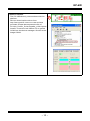
The procedure of using ICE module to download the HEX to MCU:
1. Execute ICP Programer.exe
2. Select MCU part no. of MPC82E516
3. Click
for selecting down load program.
4. Click
for download the program to MCU.
– 22 –
GP-6W
If using ICE module via Keil C debug program, must install ICE driver to Keil C file.
1.Execute the setup.exe which is on the file 8051_OCD_ICE_For_Keil_v2.50-1\(1)
Database Installer.
2.Click
to load Keil C.
3.Click
and finish it.
– 23 –
GP-6W
4. The Testing way of MPPT
The Design of Perturbation & Observation(P&O) (Hill-climbing)
As the sunlight intensity change is similar to ambient temperature change which is
a slow processl, the sampling is no need high real-time, once every a few seconds
will meet the requirements. The sampling interval can be adjusted. The initial
is short for quickly approaching the Pmax. The follow can be longer, which can
prevent the system oscillate around the Pmax. To prevent the system error, we
set 3 times for each controlled comparison. Only when the results of the 3 times
are consistent, the corresponding control strategy can be implemented, or to re-
– 24 –
GP-6W
sample comparisons. Thus, it ensure the system normal operation extramely.
1 The Hardware Circuit
Connect the solar board to P38 input. Connect P39 to P35 for detecting voltage
and current. Connect P36 to the BOOST circuit input P17 or P45. Connect the
BOOST circuit output P18 or P19 to P37 which is feedback detective voltage.
Connect another BOOST circuit output P18 or P19 to a LOAD test which is for
imitating the charging status.
The P&O method is needed to change the load amount to match with the internal
resistance of solar cells in order to achieve the Pmax. However, the real load
impedance is usually not easily programmable change. We replace it by the PWM
duty cycle of the DC / DC in this experiment. In general, the greater of PWM duty
cycle need the greater current. It will make the output load of solar energy larger
(the output impedance becomes smaller). whereas, the PWM duty cycle smaller,
the output impedance becomes larger. For a boost module, the output voltage will
increase with the PWM duty cycle larger. Therefore, if make the feedback resistor
smaller, the PWM duty cycle will be larger.
The another reason for using the step-up module is when the solar sell output
voltage is small, still can increase the voltage through the step-up module, which
– 25 –
GP-6W
make able to charge to the sell. So that, the energy can be used, will not be
wasted.
(1)1-3.2 The Software Design of P&O
The digital resistor is through the SPI interface to set. After power on, the resistor
is 5K ohm. When setting, lower the CS pin first. Then, through the SI to send DATA
(16bit), SCK is sent to the 16 pulses. , Write_Res (cs, dat) to cs said that a DC /
DC (0 for step-down, 1 for step-up), dat is resistance value (255 for 10K), formula
is (dat/255) * 10K, spi. c programs are listed is as follows.
#define CS0 P4_5
//1
#define CS1 P4_6
//1
#define SCK P4_1
//2
#define SI
//3
P1_7
#define SPI_Delay() _nop_();_nop_()
void Write_Res(unsigned char cs,unsigned char dat)
{
unsigned char temp,i;
temp=0x11;
// command
SCK=0;
if(cs==0)
{
CS0=1;
CS0=0;
}
else
{
CS1=1;
CS1=0;
}
SPI_Delay();
– 26 –
GP-6W
for(i=0;i<8;i++)
{
if((temp & 0x80)==0)
SI=0;
else
SI=1;
SCK=1;
SPI_Delay();
SCK=0;
temp<<=1;
}
temp=dat;
for(i=0;i<8;i++)
{
if((temp & 0x80)==0)
SI=0;
else
SI=1;
SCK=1;
SPI_Delay();
SCK=0;
temp<<=1;
}
CS0=1;
CS1=1;
}
– 27 –
GP-6W
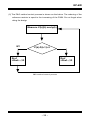
(2) The P&O method control process is shown as the below. The reducing of the
reference resistor is equal to the increasing of the PWM. Do not forget when
doing the design
Measure V(k)I(k) and p(k)
NY
Rref
=Rref+
P(k)-P(k-1)> 0
Rref
=Rref-
R
P&O method control process
– 28 –
R
GP-6W
(3) Because no need to calculate real-time, we adopted polling ADC. It use timer
to generate the timer flag (once every 5 seconds). Only when the flag is set,
then go to measure and calculate the operation point. The MPPT control
processing programs are as follows.
// MPPT processing
// P&O
void MPPT_Process()
{
unsigned char i;
for(i=0;i<3;i++)
// for 3 times
{
Sensor();
// polling read sensor for display
IN_Read();
// input convert
ppin[1]=pv*pi;
if(ppin[1]>ppin[0])
// power enlarge
{
dstime=0;
ustime++;
if(ustime>2)
// 3 times satisfied
{
ustime=0;
rref=rref-DRES;
if(rref<DRES) rref=DRES;
if(dctype==0)
// resistor reducing,
// range limit
// buck
Write_Res(0,rref);
if(dctype==1)
// boost
Write_Res(1,rref);
ppin[0]=ppin[1];
// renew record
}
}
else
{
– 29 –
GP-6W
ustime=0;
dstime++;
if(dstime>2)
{
// 3 times satisfied
dstime=0;
rref=rref+DRES;
// resistor reducing
if(rref>(255-DRES)) rref=255-DRES; // range limit
if(dctype==0)
Write_Res(0,rref);
if(dctype==1)
Write_Res(1,rref);
ppin[0]=ppin[1];
// renew record
}
}
}
}
(4) The system main process is responsible for the sampling and LCD data
display. When mflag = 1, doing once MPPT calculations. The main programs
are as follows.
void main(void)
{
IO_Init();
// IO initialization
System_Init();
Setup_Check();
if (dctype==0)
// buck
Write_Res(0,rref);
if(dctype==1)
// boost
Write_Res(1,rref);
LCD_Init();
// LCD initialization
Delay_ms(100);
// delay 0.1 sec, wait LCD finish
LCD_Cmd(0x80);
// specify to row1 column1 of LCD
CHARGE=1;
DISCHARGE=1;
// charge switch ON
// discharge switch ON
– 30 –
GP-6W
Delay_ms(100);
// delay 0.1 sec
Sensor();
// record first power
// polling reading sensor for display
IN_Read();
LOAD_Read();
// input convert
// output convert
ppin[0]=pv*pi;
while(1)
{
Sensor();
// polling reading sensor for display
IN_Read();
LOAD_Read();
// input convert
// input convert
if(OSHORT_flag==1)
// input short circuit feedback 3_5
{
if(OSET==0) {
OSHORT_flag=0;
disp_buf2[13]='D';
DISCHARGE=1;
}
}
if(ISHORT_flag==1)
// input short circuit feedback P3_5
{
if(ISET==0)
{
ISHORT_flag=0;
disp_buf1[13]='C';
CHARGE=1;
}
}
if(P3_6==0)
// change display content
{
Delay_ms(10);
// delay
– 31 –
GP-6W
if(P3_6==0)
{
if(dispmode==0) dispmode=1;
else dispmode=0;
}
}
Message();
if(uart_received_finished==TRUE)
{
rs232_process();
uart_received_finished=FALSE; // process finished
}
if(MPPT==0)
// do MPPT
{
MPPT_flag=1;
if(mflag==1)
{
MPPT_Process(); // MPPT process
mtime=0;
mflag=0;
}
}
else
MPPT_flag=0;
}
}
– 32 –
GP-6W
2. Three-point-weighting comparison(TPWC)
(1) As the below chart, measure B point data first. And then, after reducing the
Δ PWM, and measure A point. Increase the double of Δ PWM, and measure
C points. Then, determine the TAG and decide the PWM to increase or
decrease.
(refer the resistor increasing or decreasing.)
N
Tag1=-1
Y
Tag1=-1
PC-PB>0
N
Tag2=-1
PC-PB>0
Tag1+Tag2==
-2
Y
Y
Y
Tag1+Tag2==
0
Set Rref value
TPWC control chart
– 33 –
Tag2=-1
GP-6W
(2) Hardware circuit
Set as the previous.
(3) TPWC program design
Main program as below. The below is only for MPPT program.
// MPPT manage
// TPWC
void MPPT_Process()
{
Sensor();
// polling for reading sensor value for display
IN_Read();
// input convert
ppin[1]=pv*pi;
// B point power
rref=rref+DRES;
// decreas PWM
if(rref>(255-DRES)) rref=255-DRES; // range limit
if(dctype==0)
Write_Res(0,rref);
if(dctype==1)
Write_Res(1,rref);
Sensor();
// polling for reading sensor value for display
IN_Read();
// input convert
ppin[0]=pv*pi;
rref=rref-2*DRES;
// A point power
// increas PWM
if(rref<DRES) rref=DRES;
// range limit
if(dctype==0)
Write_Res(0,rref);
if(dctype==1)
Write_Res(1,rref);
Sensor();
IN_Read();
ppin[2]=pv*pi;
if(ppin[2]>=ppin[1])
// polling for reading sensor value for display
// input convert
// C point power
// C>=B
tag1=1;
else
tag1=-1;
– 34 –
GP-6W
if(ppin[0]>=ppin[1])
// A>=B
tag2=-1;
else
tag2=1;
tag=tag1+tag2;
if(tag==2)
{
// not necessary to increase PWM, because already done.
}
if(tag==-2)
{
rref=rref+2*DRES;
if(rref>(255-DRES)) rref=255-DRES; // range limit
}
if(tag==0)
{
rref=rref+DRES;
if(rref>(255-DRES)) rref=255-DRES; // range limit
}
if(tag!=2)
{
if(dctype==0)
Write_Res(0,rref);
if(dctype==1)
Write_Res(1,rref);
}
}
– 35 –
GP-6W
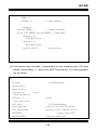
3. Design of Slope-comparison(SC)
(1) The slope-comparison (SC) is based on P&O. It is observed that the location
is in the left or right of the Pmax. When on the left, the slope left is positive, on
the right, the slope is negative. They are shown in the below Figure. That is,
It determines the movement direction of working point by the change of solar
input and power.
Pmaz
Negative
Input power
V.S.
input voltage
Positive
Slope change
Input
The control process as the below.
Measure (k)I(k), count up P(k)
N
Y
P(k)-P(k-1)>0
Y
V(k)-V(k-1)>0
Rref
=Rref+△R
Rref
=Rref-△R
N
N
Y
V(k)-V(k-1)>0
Rref
=Rref-△R
The control processes of the SC
– 36 –
Rref
=Rref+△R
GP-6W
(2) The Circuit Design of the Hardware
Same default as the previous.
(3) The programs design of the Software
The main programs are same as the before. Here are only the processing
programs of MPPT.
// MPPT processing
// SC
void MPPT_Process()
{
unsigned char i;
for(i=0;i<3;i++)
// for 3 times
{
Sensor();
// polling reading sensor for display
IN_Read();
// input convert
LOAD_Read();
// Output convert
pvin[1]=pv;
ppin[1]=pv*pi;
if(ppin[1]>ppin[0])
{
dstime=0;
ustime++;
if(ustime>2)
// 3 times satisfied
{
ustime=0;
if(pvin[1]>pvin[0])
{
rref=rref+DRES; // resistor increasing,PWM decreasing
if(rref>(255-DRES)) rref=255-DRES;
}
else
{
rref=rref-DRES;
// resistor decreasing, PWM
increasing
if(rref<DRES) rref=DRES;
}
if(dctype==0)
Write_Res(0,rref);
– 37 –
GP-6W
}
else
{
}
}
}
if(dctype==1)
Write_Res(1,rref);
ppin[0]=ppin[1];
pvin[0]=pvin[1];
// re-new record
}
ustime=0;
dstime++;
if(dstime>2)
// 3 times satisfied
{
dstime=0;
if(pvin[1]>pvin[0])
{
rref=rref+DRES; // resistor increasing,PWM decreasing
if(rref>(255-DRES)) rref=255-DRES; // range limit
}
else
{
rref=rref-DRES; // resistor decreasing, PWM increasing
if(rref<DRES) rref=DRES;
// range limit
}
if(dctype==0)
Write_Res(0,rref);
if(dctype==1)
Write_Res(1,rref);
ppin[0]=ppin[1];
// re-new record
pvin[0]=pvin[1];
}
– 38 –
GP-6W
5. Specification & Caution
Specification:
1. Solar chip board: 8V(Max) 787 mA (Max)- under the sunlight. If you are indoor
under fluorescent illumination, it's not enough. Please use halogen lamps or
other light source.
2. Rechargeable battery: no. 3 rechargeable battery x 4, 1.2V 800mA.
3. Adapter 9V 0.5A, positive pole inside.
Caution:
1. The product of the DC to AC function is only to provide users of solar energy
conversion experiments. It can not provide for real life use.
2. The product of temperature and illumination functions are only for experimental
reference. There is a certain difference with the fact. If you would like to
improve the accuracy, will need to modify the program by yourself.
3. The halogen light with this product is only for simulating the sunlight. During
the operation, the halogen lamp will become hot. Please do not contact it to
prevent burns. At the meantime, avoid eye contact for too long to prevent eye
injury.
4. This product is provided the no. 3 rechargeable batteries holder. Please do not
put other type of battery to avoid danger.
5. The each terminal connection between the experiment of this product is for
various modules. Please refer the operation to avoid a short circuit happen.
6. We should use the wind power generation kit in an open place. In order to
avoid accident during the blades rotating. The whole experiment must be
accompanied by teachers.
7. The product use solar panels. The maximum output voltage is 8V, current is
787mA. The total output power is 6 W.
8. The solar panels must have adequate exposure to sunlight or simulated light
source for reaching the biggest voltage and current putput.
9. For each unit experiment, please allow the solar panels to maintain an enough
sunlight or light source for completeing the operation.
– 39 –
GP-6W
10. The optional accsesories of this product: Halogen lamp and Wind power
generation kit.
11. During the experiment, please make sure the input is rectified or un-rectified.
The rectified power source input is P41. The un-rectified is P40.
12.The “Load module” may be hot during the wroking. Please pay attention to
safety and not to remain a long time using.
13. The structure of solar panels is relatively weak. Please be careful during the
use, collection and transportation. Do not drop or shock.
14. During using the halogen module, do not shake violently or quickly adjust
lighting angle or orientation. Becuase the tungsten will produce heat and be
broken easily.
15. If the solar panels are damaged by external force, we will charge the repair
cost for the materials and replacement.
16. If you would like to recover the manufacturer default, please use the ICE to
load the GREEN. HEX which in the Boot Loader file to the MCU.
6. Experiment Content
1.Experiment content
● Observe I/V, V/P and MPP characteristic curve of solar power module.
● Set the output I/V of the solar module according to the incident angle.
● DC to DC converter module design.
● DC to AC inverter module experiment.
● Basic load experiment to observe the solar module I/V change.
● Charging and discharging function of the battery.
● MPPT algorithm.
● Integrate all of the above experiments. So we can exactly understand
regeneration and recycling of green power.
– 40 –
GP-6W
2. Teaching book content
Ch1. Instruction of green power
Ch2. Instruction of the lab
Ch3. Instruction of software development tool
Ch4. Learning C language
Ch5. Feature and basic experiment of MPC82E516
Ch6. Control of LCM display
Ch7. Control of analog to digital
Ch8. Control of PWM
Ch9. Theory of DC to DC
Ch10. Control of battery charging & discharging
Ch11. MPPT algorithm
Ch12. Design of DC to AC
– 41 –
GP-6W
7. Standard & Optional Accessories
Standard Accessories:
1.Main unit x 1
2.Adapter 9V~12V/500mA, positive pole inside x 1
3.USB cable x 1
4.10cm 2pin cable with 3.96mm terminal x 1
5.30cm 2pin cable with 3.96mm terminal x 2
6.34cm 3pin cable with 3.96mm terminal x 5
7.No. 3 rechargeable battery x 4
8.CD X 1
Optional Accessories:
1.Halogen lamp ,250W x 1
2.Wind power generation kit
– 42 –
Doc ume nt No :PME-1 2 0 5 0 7 - V. B
E-mail:[email protected]
WEB:www.leap.com.tw
www.leaptronix.com