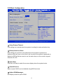
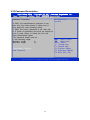
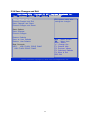
1
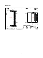
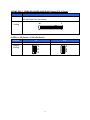
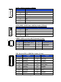
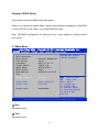
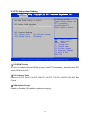
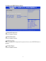
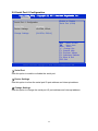
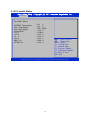
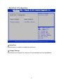
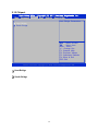
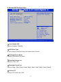
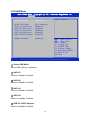
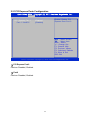
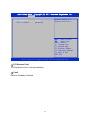
WEX-N2600
User Manual
Intel N2600
Rev.01, Apr. 2013
www.cjb.it
Statement
All rights reserved. No part of this publication may be reproduced in any form or by
any means, without prior written permission of the publisher.
All trademarks are the properties of the respective owners.
All product specifications are subject to change without prior notice
Packing List
□ WEX-N2600
□ Driver CD (Include user’s manual)
2
Contents
Chapter 1 Product Information ...................................................................................5
1.1 Block Diagram ............................................................................................... 5
1.2 Features ........................................................................................................ 6
1.3 PCB Layout ................................................................................................... 8
1.4 Jumper Setting .............................................................................................. 9
1.5 Connector Function List .............................................................................. 13
1.6 Internal Connector Pin Define ..................................................................... 14
Chapter 2 BIOS Setup.............................................................................................. 19
2.1 Main Menu .................................................................................................. 19
2.2 Advanced Menu .......................................................................................... 21
2.3 PCI Subsystem Setting ............................................................................... 22
2.4 Advanced BIOS Feature Setup ................................................................... 23
2.5 CPU Configuration ...................................................................................... 24
2.6 SATA Configuration ..................................................................................... 25
2.7 USB Configuration ...................................................................................... 26
2.8 Super IO Configuration ............................................................................... 27
2.9 Serial Port 0 Configuration .......................................................................... 28
2.10 Serial Port 1 Configuration ........................................................................ 29
2.11 Parallel Port Configuration......................................................................... 31
2.12 Pc Health Status ........................................................................................ 32
2.13 Serial Super IO Configuration ................................................................... 33
2.14 Serial Port Configuration ........................................................................... 34
2.15 Chipset ...................................................................................................... 35
2.16 Memory Information .................................................................................. 36
2.17 Chipset Configuration ................................................................................ 37
2.18 Intel IGD Configuration .............................................................................. 38
2.19 PCI Express Root Ports Configuration ...................................................... 41
2.20 USB Mode ................................................................................................. 42
2.21 PCI Express Ports Configuration ............................................................... 44
2.22 Boot Configuration .................................................................................... 45
2.23 Password Description ............................................................................... 47
2.24 Save Changes and Exit ............................................................................. 48
Chapter 3 Drivers Installation ................................................................................... 49
3.1 Intel Chipset Device Software ..................................................................... 49
3.2 Intel Graphic Media Accelerator Driver ........................................................ 52
3.3 LAN Driver................................................................................................... 55
3
3.4 Audio Driver................................................................................................. 57
Appendix-A Watchdog .............................................................................................. 58
Appendix-B GPIO ..................................................................................................... 62
4
Chapter 1 Product Information
This chapter introduces the product features, jumper and connector information.
1.1 Block Diagram
VCPU_PWROK
ISL95837HRZ
V1.05_PWROK
VR_ON
PGOOD
PGOODG
P 29
GFX_PWRGD
VGA
9VRS4339BKLF/MLF56
DP
P 04
D2 Series / N2 Series
eDP
CH7511
PLTRST-
P 25
25MHZ
P 03
Intel ATOM
P 19
DP Signal CONN to DVI-D
LVDS 18/24bit P 25
SM Bus
ALL_SYS_PWRGD
SO-DIMM
DDR3 800/1066MHz
SM Bus
P 08
PLTRST_N
RESET#
H_PWRGD
PWRGOOD
27MHZ
27MHZ
DDR3_PWROK
DDR3_DRAM_PWROK
SYS_PWRGD_TPT
DDR3_VCCA_PWROK
P 04,05,06.07
DMI 4 Lanes
RTC
HD Audio
CODEC_ALC662 P 21
Intel
CG82NM10
NM10
SATA
SATA1 CONN P 17
SATA2 CONN or CFAST Socket
SATA
P 17
USB 2.0 x2
32.768KHZ
PLTRST-
PCIe x1
PLTRST-
PCIe x1
PLTRST-
LAN1_RTL8111E P 22
25MHZ
LAN2_RTL8111E P 23
25MHZ
PCIe x1
USB 2.0
mini-PCIe Slot
SLP_S3#
SLP_S3_N
RSMRST#
RSMRST#
SLP_S4#
SLP_S4_N
PM_PWRBTN_N
PWRBTN#
SLP_S5#
SLP_S5_N
SYS_RESET#
PLTRST#
PLTRST_R_N
P 17
FP_RST_N
P 24
PCIRST#
SYS_PWRGD_TPT
PWROK
ALL_SYS_PWRGD
VRMPWRGD
CPUPWRGD
SPI
PSIN
SPI P 18
H_PWRGD
P 09,10,11
LPC I/F
PS_ON-
SIO_W83627EHG
PLTRST-
PM_PWRBTN_N
PLTRST-
SIO_ F81216D P 13
SIO_PWROK
WDTO_N
SIO_RSMRST_N
P 12
COM3 P 16
DIO P 20
LPT P 18
COM1 P 15
KB&MSP 18
5
COM2 P 15
COM4 P 16
1.2 Features
SystemProcessor/
Chipsets
Memory
Display
Ethernet
Audio
SATA
Expansion Bus
Onboard
Pin-Header
Rear I/O
Power
Processor
Intel ATOM Processor D2550/N2600
processor on board
Chipset
Intel D2550 + NM10, Intel N2600 + NM10
BIOS
AMI
Technology
One 204-pin DDR3 1066 SO-DIMM
SDRAM, upgradable to 4GB
Chipset
Intel D2550 integrated
VRAM
Share with System memory
Resolution
Analog Display: Up to 2048 x 1536 (QXGA)
LVDS
24bit, Dual channel
LVDS Resolution
Digital LVDS: Up to 1920 x 1200
Dual Display
CRT+LVDS, CRT+DP, LVDS+DP
Interface
Dual 10/100/1000 Mbps
Controller
Realtek 8111E GbE
Interface
High Definition Audio
Controller
Realtek ALC662 HD CODEC
Max. Data
Transfer
300 MB/s
Port
1
Mini-PCIe
1
LVDS
1
USB 2.0
2
COM
3
Parallel
1
DP
1
Audio Header
1 (Mic.-In, Line-in, Line-out)
C-Fast
1
DIO *Note1
8-bit Digital I/O (4 In + 4 Out)
PS/2
1 (K/B and Mouse)
COM
1 x (RS232/422/485), support 5V & 12V by
jumper selector
VGA
1
LAN
2 x RJ45
USB 2.0
2
Connector Type
4-pin DC-in power connector
6
Mode
AT/ATX Mode support (by jumper selector)
Interval
Programmable 1~255 sec./min.
Output
System reset
Operating Temp.
0°C~ 60°C
Environment
*Note2
Storage Temp.
-20°C~ 80°C
Relative
Humidity
0%~ 95% (non-condensing)
Form Factor
Dimension (L*W)
146mm x 102mm
Watchdog Timer
*Note:
1. Digital I/O: - Input: 12V-tolerance & TTL inputs with ESD protection. - Output: Open-drain
outputs with minimum100mA sinking capability.
2. Laboratory Stress Test Results: - Operating Temperature: 0°C ~ 60°C (0%~95% R.H.,
non-condensing) - Cold Boot Temperature: -40°C
7
1.3 PCB Layout
Top view
PWR1
H2 JLVDS1
KB_MS1
JLVDS_SEL1
LCD1
DB1
JCMOS
BAT1
H4
INV1
AUDIO1
MINI-PCIE1
JFRONT
DIO1
LPC1
U12
U7
JSPI1
LPT1
USB2
COM1
COM3
COM4
JCOM2_SEL1
CPUFAN1
SATA_PWR1
JCOM2
JPWR_SEL1
H3
H1
VGA1
LAN1
COM2
8
LAN2
USB1
SATA1
Bottom View
CFAST1
SO-DIMM1
9
1.4 Jumper Setting
JCMOS: CMOS Clear (2.54mm)
Pin No.
Function
1-2
2-3
Normal Operation (Default)
Clear CMOS Contents
3 2 1
3 2 1
Jumper
Setting
JCOM2: (5V/12V/RI) Select (2.54mm)
Pin No.
1-2
3-4
5-6
Function
+5V
Modem Ring In
(Default)
+12V
5 3 1
5 3 1
5 3 1
6 4 2
6 4 2
6 4 2
Jumper Setting
JCOM2_SEL: COM2 (RS-232/RS-422/RS-485) Select (1/3) (2.0mm)
Pin No.
5-6, 11-13, 12-14, 19-21, 20-22
3-4, 9-11, 10-12, 17-19, 18-20
Function
RS-232 (Default)
RS-422
23
1
23
1
24
2
24
2
Jumper
Setting
JCOM2_SEL: COM2 (RS-232/RS-422/RS-485) Select (2/3) (2.0mm)
Pin No.
1-2, 9-11, 10-12, 23-24
15-16
Function
RS-485
RS-422 RX 100Ω Termination
Jumper
Setting
23
1
23
1
24
2
24
2
10
JCOM2_SEL1: COM2 (RS-232/RS-422/RS-485) Select (3/3) (2.0mm)
Pin No.
Function
7-8
RS-422 TXD Pair 100Ω (Not recommended)/
RS-485 Data Pair Termination
Jumper
Setting
23
1
24
2
JLVDS1: LCD Power (+3.3V/+5V) Select
Pin No.
1-2
2-3
Function
LCD Power +3.3V (Default)
LCD Power +5V
Jumper
Setting
1
2
3
1
2
3
11
JLVDS_SEL1: LVDS Panel Type Select
Jumper Setting
LVDS Panel Type
2 4 6 8
800*600/18bit
Single Channel
1 3 5 7
2 4 6 8
1024*768/18bit
Single Channel
1 3 5 7
2 4 6 8
1024*768/24bit
Single Channel
1 3 5 7
2 4 6 8
1280*768/18bit
Single Channel
1 3 5 7
2 4 6 8
1280*800/18bit
Single Channel
1 3 5 7
2 4 6 8
1280*960/18bit
Single Channel
1 3 5 7
2 4 6 8
1280*1024/24bit
Dual Channel
1 3 5 7
2 4 6 8
1366*768/18bit
Single Channel
1 3 5 7
2 4 6 8
1366*768/24bit
Single Channel
1 3 5 7
12
2 4 6 8
1400*900/24bit
Dual Channel
1 3 5 7
2 4 6 8
1400*1050/24bit
Dual Channel
1 3 5 7
2 4 6 8
1600*900/24bit
Dual Channel
1 3 5 7
2 4 6 8
1680*1050/24bit
Dual Channel
1 3 5 7
2 4 6 8
1600*1200/24bit
Dual Channel
1 3 5 7
2 4 6 8
1920*1080/24bit
Dual Channel
1 3 5 7
2 4 6 8
1920*1200/24bit
Dual Channel
1 3 5 7
JPWR_SEL1: AT/ATX Mode Select
Pin No.
Function
Jumper
Setting
1-2
2-3
AT Mode
ATX Mode (Default)
1
2
3
1
2
3
13
1.5 Connector Function List
Connector
Function
AUDIO1
Audio Amplifier Output with Box-header
COM1, 3, 4
Serial Port with Box-header
COM2
Serial Port with DSUB-9P connector
CPUFAN1
CPUFAN 3-pin connector
DIO1
Digital I/O with Pin-header
INV1
Inverter with Box-header
JFRONT
Front Panel with Pin-header
KB_MS1
Keyboard and mouse connector
LAN1, 2
LAN connector
LCD1
LVDS Panel Signal with Box-header
LPC1
Debug Port with Pin-header
LPT1
Parallel Port with Box-header
MINI-PCIE1
Mini PCI Express connector
PWR1
ATX 2x2 connector (DC12V-IN)
SATA1
SATA connector
SATA_PWR1,
SATA Power with Box-header
USB1
USB0/1 Port connector
USB2
USB2/3 connector with Pin-header
DB1
External DVI or HDMI Box-header
CFAST1
C-FAST Connector
VGA1
VGA connector
14
Note
1.6 Internal Connector Pin Define
AUDIO: Audio Amplifier Output with Wafer connector (2.0mm)
2
1
10
9
Pin No.
Signal
Pin No.
Signal
1
Line-In Right
2
Line-In Left
3
Line-In Jack Detect
4
MIC Jack Detect
5
MIC-In Right
6
MIC-In Left
7
Line-Out Jack Detect
8
Audio Ground
9
Line-Out Right
10
Line-Out Left
COM1, 3, 4: Serial Port with Box-header (2.0mm)
1
2
10
9
Pin No.
Signal
Pin No.
Signal
1
DCD
2
DSR
3
RXD
4
RTS
5
TXD
6
CTS
7
DTR
9
Ground
8,10
RI/+5V/+12V
COM2: RS 232 Serial Port with DSUB-9P connector (1/3)
Pin No.
1
6
2
7
3
8
4
9
5
Signal
Pin No.
Signal
1
DCD
2
RXD
3
TXD
4
DTR
5
Ground
6
DSR
7
RTS
8
CTS
9
RI/+5V/+12V
COM2: RS 422 Serial Port with DSUB-9P connector (2/3)
Pin No.
1
6
2
7
3
8
4
9
5
Signal
Pin No.
Signal
1
DATA TX-
2
DATA TX+
3
DATA RX+
4
DATA RX-
5
NC
6
NC
7
NC
8
NC
9
NC
15
COM2: RS 485 Serial Port with DSUB-9P connector (3/3)
Pin No.
1
6
2
7
3
8
4
9
5
Signal
Pin No.
Signal
1
DATA-
2
DATA+
3
NC
4
NC
5
NC
6
NC
7
NC
8
NC
9
NC
CPUFAN: 3Pin FAN connector
1
Pin No.
3
Signal
1
Ground
2
Fan Power (+12V)
3
Speed Sense
DIO: Digital I/O with Pin-header (2.00mm)
2
1
10
11
1
Pin No.
Signal
Signal
1
DIO-Out0
2
DIO-In0
3
DIO-Out1
4
DIO-In1
5
DIO-Out2
6
DIO-In2
7
DIO-Out3
8
DIO-In3
9
+12V
10
+5V
11
Ground
INV1: Inverter with Box-header (2.50mm)
Pin No.
5
Pin No.
Signal
1
+12V
2
+12V
3
Ground
4
Inverter Brightness control
5
Inverter Enable
16
JFRONT: Front Panel Connector with Pin-header (2.54mm)
1
9
2
Pin No.
10
Signal
Pin No.
Signal
1
Power LED +
(+5V, 470Ω)
2
Power LED – (Ground)
3
HDD LED + (470Ω)
4
HDD LED -
5
Suspend LED +
(+V5S, 470Ω)
6
Suspend LED -
7
Reset Switch +
8
Reset Switch – (Ground)
9
Power Switch +
10
Power Switch – (Ground)
KB_MS1: Keyboard and mouse connector (2.00mm)
1
Pin No.
6
S gnal
1
PS2 Power (+5V)
2
PS2 Mouse Data
3
PS2 Mouse Clock
4
PS2 Keyboard Data
5
PS2 Keyboard Clock
6
PS2 Ground
LCD1: LVDS Panel Signal with Box-header (1.0mm)
1
29
2
30
Pin No.
Signal
Pin No.
Signal
1
Ground
2
Ground
3
LA_DC3+
4
LA_DC3-
5
LA_CLK+
6
LA_CLK-
7
LA_DC2+
8
LA_DC2-
9
LA_DC1+
10
LA_DC1-
11
LA_DC0+
12
LA_DC0-
13
Ground
14
Ground
15
LB_DC7P
16
LB_DC7N
17
LB_CLK2P
18
LB_CLK2N
19
LB_DC6P
20
LB_DC6N
21
LB_DC5P
22
BL_DC5N
23
LB_DC4P
24
LB_DC4N
25
Ground
26
Ground
27
LVDS Power
28
LVDS Power
29
LVDS Power
30
Note1: LVDS Power = +5V or +3.3V (Default)
17
LVDS Power
LPC1: Debug Port with Pin-header (2.0mm)
1
9
2
8
Pin No.
Signal
Pin No.
Signal
1
LAD0
2
LPC Reset#
3
LAD1
4
LFRAME#
5
LAD2
6
+3.3V
7
LAD3
8
Ground
9
LPC33MHz
10
NC
LPT1: Parallel Port with Box-header (2.0mm)
Pin No.
1
13
1
14
26
2
Signal
4
Signal
1
Strobe#
14
Auto Form Feed#
2
Data 0
15
Error#
3
Data 1
16
Initialization#
4
Data 2
17
Printer Select IN#
5
Data 3
18
Ground
6
Data 4
19
Ground
7
Data 5
20
Ground
8
Data 6
21
Ground
9
Data 7
22
Ground
10
Acknowledge#
23
Ground
11
Busy
24
Ground
12
Paper Empty
25
Ground
13
Printer Select
26
Ground
PWR1: ATX 2x2 +12V Input (4.20mm)
Pin No.
3
Pin No.
Signal
Pin No.
Signal
1
Ground
2
Ground
3
+12V
4
+12V
18
SATA1: SATA Connector (2.50mm)
Pin No.
1
7
Signal
1
Ground
2
TX+
3
TX-
4
Ground 1
5
RX-
6
RX+
7
Ground 2
SATA_PWR1: SATA Power with Box-header (2.50mm)
1
Pin No.
4
Signal
1
+5V
2
Ground
3
Ground
4
+12V
USB2/3: USB connector with Pin header (2.0mm)
2
8
1
7
Pin No.
Signal
Pin No.
Signal
1
USB Power (+5V)
2
USB Power (+5V)
3
USB DATA-
4
USB DATA-
5
USB DATA+
6
USB DATA+
7
Ground
8
Ground
DB1: External DVI or HDMI Box-header (2.0mm)
1
19
2
20
Pin No.
Signal
Pin No.
Signal
1
TX0_DP
2
TX3_DP
3
TX0_DN
4
TX3_DN
5
Ground
6
Ground
7
TX1_DP
8
DDC_SCL
9
TX1_DN+
10
DDC_SDA
11
Ground
12
Ground
13
TX2_DP
14
HPD_N
15
TX2_DN
16
+V5
17
Ground
18
Ground
19
+V3.3
20
+V3.3
19
Chapter 2 BIOS Setup
This chapter introduces BIOS setup information.
Power on or reboot the system board, when screen appears message as “Press DEL
to enter SETUP.” Press <DEL> to run BIOS SETUP Utility.
Note: The BIOS configuration for reference only, it may subject to change without
prior notice.
2.1 Main Menu
Main
Main
Aptio Setup Utility - Copyright (C) 2011 American Megatrends, Inc .
Advanced Chipset Boot Security Save & Exit
BIOS Information
BIOS Vendor
Core Version
Compliancy
Project Version
Model Name
BIOS Version
Build Date and
Time
American Megatrends
4.6.5.1
UEFI 2.3; PI 1.2
1APJK 0.14
WECX-D25501
RA05
08/24/2012 22:47:05
System Language
[English]
System Date
System Time
[Mon 11/12/2012]
[14:47:18]
Access Leve1
Administrator
Choose the system
default language
: Select Screen
: Select Item
Enter : Select
+/- : Change Opt .
F1: General Help
F2: Previous Values
F3: Optimized Defaults
F4: Save & Exit
ESC: Exit
Version 2.14.1219. Copyright (C) 2011 American Megatrends, INC.
□ Date
Set system date.
□ Time
Set system time.
20
2.2 Advanced Menu
This section allows you to configure CPU and other system devices for basic operation
through the following sub-menus.
Main
Aptio Setup Utility - Copyright (C) 2011 American Megatrends, Inc .
Advanced
Advanced Chipset Boot Security Save & Exit
Legacy OpROM Support
Onboard PXE OpROM
Wake On PCIe Lan
Wake On Ring
Launch Storage OpROM
PCI
ACPI
CPU
IDE
USB
Super
H/W
Second
[Disabled]
[Disabled]
[Disabled]
[Enabled]
Subsystem Settings
Settings
Configuration
Configuration
Configuration
IO Configuration
Monitor
IO Configuration
Boot Option for relTek
8111E NIC.
: Select Screen
: Select Item
Enter : Select
+/- : Change Opt .
F1: General Help
F2: Previous Values
F3: Optimized Defaults
F4: Save & Exit
ESC: Exit
Version 2.14.1219. Copyright (C) 2011 American Megatrends, INC.
WATX‐Q670 BIOS RA01 20120104
□ Onboard PXE OpROM
Choices: Disabled, Enabled.
□ Wake On PCIe Lan
Choices: Disabled, Enabled.
□Wake On Ring
Choices: Disabled, Enabled.
□ Launch Storage OpROM
Enabled: Use this setting to specify that legacy PCI option ROMs for PCI storage
devices are to be loaded and executed.
21
2.3 PCI Subsystem Setting
Aptio Setup Utility - Copyright (C) 2011 American Megatrends, Inc .
Advanced
PCI Bus Driver Versio V 2.05.01
PCI Option ROM Handling
PCI ROM Priority
[EFI Compatible ROM]
In case of multiple
Option ROMs (Legacy and
EFI Compatible) ,
specifies what PCI
Option ROM to launch.
PCI Common Settings
PCI Latency Timer
[32 PCI Bus Clocks]
VGA Palette Snoop
[Disabled]
: Select Screen
: Select Item
Enter : Select
+/- : Change Opt .
F1: General Help
F2: Previous Values
F3: Optimized Defaults
F4: Save & Exit
ESC: Exit
Version 2.14.1219. Copyright (C) 2011 American Megatrends, INC.
□ PCI ROM Priority
In case of multiple optional ROMs (Legacy and EFI Compatible), specifies what PCI
option ROM to launch.
□ PCI Latency Timer
Choices: 32 PCI, 64 PCI, 96 PCI, 128 PCI, 160 PCI, 192 PCI, 224 PCI, 248 PCI Bus
Clocks.
□ VGA Palette Snoop
Enable or Disable VGA palette registers snooping.
22
2.4 Advanced BIOS Feature Setup
Aptio Setup Utility - Copyright (C) 2011 American Megatrends, Inc .
Advanced
Enables or Disables
BIOS ACPI Auto
Configuration.
ACPI Settings
Enable ACPI Auto Conf [Disabled]
Enable Hibernation
ACPI Sleep State
S3 Video Repost
[Enabled]
[S3 (Suspend to RAM)]
[Disabled]
: Select Screen
: Select Item
Enter : Select
+/- : Change Opt .
F1: General Help
F2: Previous Values
F3: Optimized Defaults
F4: Save & Exit
ESC: Exit
Version 2.14.1219. Copyright (C) 2011 American Megatrends, INC.
□ Enable ACPI Auto Conf
Choices: Disabled, Enabled.
□ Enable Hibernation
Choices: Disabled, Enabled.
□ ACPI Sleep State
Select the highest ACPI sleep state the system will enter, when SUSPEND button is
pressed.
□ S3 Video Repost
Choices: Disabled, Enabled.
23
2.5 CPU Configuration
Aptio Setup Utility - Copyright (C) 2009 American Megatrends, Inc .
Advanced
CPU Configuration
Processor Type
EMT64
Processor Speed
System Bus Speed
Rato io Status
Actual Ratio
System BUS Speed
Processor Stepping
Microcode Revision
L1 Cache RAM
L2 Cache RAM
Processor Core
Hyper-Threading
Intel(R) Atom(TM) CPU
Not Supported
1865 MHZ
533 MHZ
14
14
533 MHZ
30661
265
2x56 k
2x512 k
Dual
Supported
[Enabled]
Hyper-Threading
[Enabled]
Execute Disable Bit
Limit CPUID Maximum [Disabled]
Enabled for Windows XP
and Linux (OS optimized
for Hyper‐Threading Technology) and
Disabled for other OS
(OS not optimized for
Hyper‐Threading
Technology).
: Select Screen
: Select Item
Enter : Select
+/- : Change Opt .
F1: General Help
F2: Previous Values
F3: Optimized Defaults
F4: Save & Exit
ESC: Exit
Version 2.14.1219. Copyright (C) 2011 American Megatrends, INC.
WATX‐Q670 BIOS RA01 20120104
□ Hyper-Threading
Choices: Disabled, Enabled.
□ Execute Disabled Bit
Choices: Disabled, Enabled.
□ Limit CPUID Maximum
Disabled for Windows XP
Choices: Disabled, Enabled.
24
2.6 SATA Configuration
Aptio Setup Utility - Copyright (C) 2011 American Megatrends, Inc .
Advanced
SATA Port0
SATA Port1
Not Present
Not Present
SATA Controller(s)
[Enabled]
Configure SATA as
[IDE]
SATA Ports (0‐3) Device
Names if Present and
Enabled.
Misc Configuration for hard disk
: Select Screen
: Select Item
Enter : Select
+/- : Change Opt .
F1: General Help
F2: Previous Values
F3: Optimized Defaults
F4: Save & Exit
ESC: Exit
Version 2.14.1219. Copyright (C) 2011 American Megatrends, INC.
□ Serial-ATA Controller(s)
Choices: Disabled, Enabled.
□ Configure SATA as
Choices: IDE/AHCI
25
2.7 USB Configuration Aptio Setup Utility - Copyright (C) 2009 American Megatrends, Inc .
Advanced
USB Configuration
USB Devices
1 Drive, 1 Keyboard
Legacy USB Support
EHCI Hand-off
[Enabled]
[Disabled]
USB hardware delays a
USB transfer time-out
Device reset
time-out
Device power-up delay
[20 sec]
[20 sec]
[Auto]
Mass Storage Devices:
USB FLASH DRIVE PMAP
[Auto]
Enables Legacy USB support. AUTO option
disables legacy support
if no USB devices are
connect. DISABLE
option will keep USB
devices available only
for EFI applications.
: Select Screen
: Select Item
Enter : Select
+/- : Change Opt .
F1: General Help
F2: Previous Values
F3: Optimized Defaults
F4: Save & Exit
ESC: Exit
Version 2.14.1219. Copyright (C) 2011 American Megatrends, INC.
□ Legacy USB Support
Set [Enabled] if you need to use any USB 1.1/2.0 devices in the operating system that
does not support or have any USB 1.1/2.0 drivers installed. Such as DOS and SCO
Unix.
□ EHCI Hand-off
This is a workaround for OSs without EHCI hand-off support. The EHCI ownership
change should be claimed by EHCI driver.
□ USB transfer time-out
Choices: 1, 5, 10, 20 sec.
□ Device Reset time-out
USB mass storage device starts unit command timeout.
Choices: 10, 20, 30, 40 sec.
26
□ Device power-up delay
This setting determines the maximum time for USB device will take before reporting
to the controller.
□ USB Flash Drive PMAP
This items shows when user inserts USB drive.
27
2.8 Super IO Configuration
Aptio Setup Utility - Copyright (C) 2011 American Megatrends, Inc .
Advanced
Super IO Configuration
Winbond W83627EHG
Super IO Chip
Serial Port 0 Configuration
Serial Port 1 Configuration
Parallel Port Configuration
[Disabled]
Watch Dog Timer
[Disabled]
CPU smart fan control
Set Parameters of
Serial Port 0 (COMA)
: Select Screen
: Select Item
Enter : Select
+/- : Change Opt .
F1: General Help
F2: Previous Values
F3: Optimized Defaults
F4: Save & Exit
ESC: Exit
Version 2.14.1219. Copyright (C) 2011 American Megatrends, INC.
□ Watch Dog Timer
This option will determine watch dog timer.
□ CPU smart fan control
This option allows user to enable/disable the control of CPU fan speed by changing
the fan voltage.
28
2.9 Serial Port 0 Configuration
Aptio Setup Utility - Copyright (C) 2011 American Megatrends, Inc .
Advanced
Enable or Disable
Serial Port (COM)
Serial Port 0 Configuration
Serial Port
Device Settings
[Enabled]
IO=3F8h; IRQ=4;
Change Settings
[IO=3F8h; IRQ=4;]
: Select Screen
: Select Item
Enter : Select
+/- : Change Opt .
F1: General Help
F2: Previous Values
F3: Optimized Defaults
F4: Save & Exit
ESC: Exit
Version 2.14.1219. Copyright (C) 2011 American Megatrends, INC.
□ Serial Port
Use this option to enable or disable the serial port.
□ Device Settings
Use this option to show the serial port IO port address and interrupt address.
□ Change Settings
Use this option to change the serial port IO port address and interrupt address.
29
2.10 Serial Port 1 Configuration
Aptio Setup Utility - Copyright (C) 2011 American Megatrends, Inc .
Advanced
Enable or Disable
Serial Port (COM)
Serial Port 1 Configuration
Serial Port
Device Settings
[Enabled]
IO=2F8h; IRQ=3;
Change Settings
[IO=2F8h; IRQ=3;]
: Select Screen
: Select Item
Enter : Select
+/- : Change Opt .
F1: General Help
F2: Previous Values
F3: Optimized Defaults
F4: Save & Exit
ESC: Exit
Version 2.14.1219. Copyright (C) 2011 American Megatrends, INC.
□ Serial Port
Use this option to enable or disable the serial port.
□ Device Settings
Use this option to change the devioce address and interrupt address.
□ Change Settings
Use this option to change the serial port IO port address and interrupt address.
30
2.11 Parallel Port Configuration
Aptio Setup Utility - Copyright (C) 2011 American Megatrends, Inc .
Advanced
Enable or Disable
Parallel Port (LPT/LPTE)
Parallel Port Configuration
Parallel Port
Device Settings
[Enabled]
IO=378h; IRQ=7;
Change Settings
Device Mode
[IO=378h; IRQ=7;]
[Printer Mode]
: Select Screen
: Select Item
Enter : Select
+/- : Change Opt .
F1: General Help
F2: Previous Values
F3: Optimized Defaults
F4: Save & Exit
ESC: Exit
Version 2.14.1219. Copyright (C) 2011 American Megatrends, INC.
□ Parallel Port
Use this option to enable or disable the parallel port.
□ Change Settings
Use this option to change the serial port IO port address and interrupt address.
□ Device Mode
Printer mode.
31
2.12 Pc Health Status
Aptio Setup Utility - Copyright (C) 2011 American Megatrends, Inc .
Advanced
Pc Health Status
SYSTEM Temperature
CPU Temperature
CPU FAN Speed
CPUVCORE
+12 V
+1.5 V
+5 V
+3.3 V
VBAT (V)
3.3VSB (V)
:
:
:
:
:
:
:
:
:
:
C
+32
C
+34
7929 RPM
+1.22 V
+11.88 V
+1.54 V
+5.02 V
+3.32 V
+5.99 V
+3.32 V
: Select Screen
: Select Item
Enter : Select
+/- : Change Opt .
F1: General Help
F2: Previous Values
F3: Optimized Defaults
F4: Save & Exit
ESC: Exit
Version 2.14.1219. Copyright (C) 2011 American Megatrends, INC.
32
2.13 Serial Super IO Configuration
Aptio Setup Utility - Copyright (C) 2011 American Megatrends, Inc .
Advanced
Second
IO Configuration
Second
IO
Fintek F81216
Set Parameters of
Serial Port 1 (COMC)
Serial Port 1 Configuration
Serial Port 2 Configuration
: Select Screen
: Select Item
Enter : Select
+/- : Change Opt .
F1: General Help
F2: Previous Values
F3: Optimized Defaults
F4: Save & Exit
ESC: Exit
Version 2.14.1219. Copyright (C) 2011 American Megatrends, INC.
□ Serial Port 1 Configuration
□ Serial Port 2 Configuration
33
2.14 Serial Port Configuration
Aptio Setup Utility - Copyright (C) 2011 American Megatrends, Inc .
Advanced
Enable or Disable
Serial Port (COM)
Serial Port 1 Configuration
Serial Port
Device Settings
[Enabled]
Reset Required
Change Settings
[IO=3E8h; IRQ=5;]
: Select Screen
: Select Item
Enter : Select
+/- : Change Opt .
F1: General Help
F2: Previous Values
F3: Optimized Defaults
F4: Save & Exit
ESC: Exit
Version 2.14.1219. Copyright (C) 2011 American Megatrends, INC.
□ Serial Port
Use this option to enable or disable the serial port.
□ Change Settings
Use this option to change the serial port IO port address and interrupt address.
34
□ Serial Port 2 Configuration
Aptio Setup Utility - Copyright (C) 2011 American Megatrends, Inc .
Advanced
Enable or Disable
Serial Port (COM)
Serial Port 2 Configuration
Serial Port
Device Settings
[Enabled]
Reset Required
Change Settings
[IO=2E8h; IRQ=5;]
: Select Screen
: Select Item
Enter : Select
+/- : Change Opt .
F1: General Help
F2: Previous Values
F3: Optimized Defaults
F4: Save & Exit
ESC: Exit
Version 2.14.1219. Copyright (C) 2011 American Megatrends, INC.
□ Serial Port
Use this option to enable or disable the serial port.
□ Change Settings
Use this option to change the serial port IO port address and interrupt address.
35
2.15 Chipset
Main
Aptio Setup Utility - Copyright (C) 2011 American Megatrends, Inc .
Advanced Chipset
Chipset Boot Security Save & Exit
Host Bridge Parameters
Host Bridge
South Bridge
: Select Screen
: Select Item
Enter : Select
+/- : Change Opt .
F1: General Help
F2: Previous Values
F3: Optimized Defaults
F4: Save & Exit
ESC: Exit
Version 2.14.1219. Copyright (C) 2011 American Megatrends, INC.
□ Host Bridge
□ South Bridge
36
2.16 Memory Information
Aptio Setup Utility - Copyright (C) 2011 American Megatrends, Inc .
Chipset
Config Memory Frequency
and Timing Settings.
Memory Frequency and Timing
Intel IGD Configuration
******* Memory Information *******
Memory Frequency
1067MHZ(DDR3)
Total Memory
2048 MB
DIMM#0
Not Present
: Select Screen
: Select Item
Enter : Select
+/- : Change Opt .
F1: General Help
F2: Previous Values
F3: Optimized Defaults
F4: Save & Exit
ESC: Exit
Version 2.14.1219. Copyright (C) 2011 American Megatrends, INC.
□ Memory Frequency and Timing
□ Intel IGD Configuration
37
2.17 Chipset Configuration Aptio Setup Utility - Copyright (C) 2011 American Megatrends, Inc .
Chipset
Enabled OR disabled MRC
fast boot.
Memory Frequency and Timing
MRC Fast Boot
Max TOLUD
[Enabled]
[Dynamic]
: Select Screen
: Select Item
Enter : Select
+/- : Change Opt .
F1: General Help
F2: Previous Values
F3: Optimized Defaults
F4: Save & Exit
ESC: Exit
Version 2.14.1219. Copyright (C) 2011 American Megatrends, INC.
□ MRC Fast Boot
Choices: Disabled, Enabled.
□ Max TOLUD
This item allows you to select the size of TOLUD.
38
2.18 Intel IGD Configuration
Aptio Setup Utility - Copyright (C) 2011 American Megatrends, Inc .
Chipset
Intel IGD Configuration
Auto Disable IGD
IGFX – Boot Type
Backlight Active Mode
Backlight Voltage Lev
Backlight Control Lev
Active LFP
Fixed Graphics Memory
[Enabled]
[VBIOS Default]
[DC Mode]
[+3.3V]
[Step 10]
[LFP LVDS]
[128MB]
Auto disable IGD upon
external GFX detected.
: Select Screen
: Select Item
Enter : Select
+/- : Change Opt .
F1: General Help
F2: Previous Values
F3: Optimized Defaults
F4: Save & Exit
ESC: Exit
Version 2.14.1219. Copyright (C) 2011 American Megatrends, INC.
Version 2.14.1219. Copyright (C) 2011 American Megatrends, INC.
□ Auto Disable IGD
Choices: Disabled, Enabled.
□ IGFX-Boot Type
It is the option to select device by the system when it boots.
□ Backlight Active Mode
Choices: PWN Mode, DC Mode.
□ Backlight Voltage Lev
Choices: +3.3V, +5V
□ Backlight Control Lev
Choices: Step1, Step2, Step3, Step4, Step5, Step6, Step7, Step8, Step9, Step10
□ Active LFP
Choices: LFP LVDS, No LVDS
39
□ Fixed Graphics Memory
It is used by the Internal graphics device.
40
2.19 PCI Express Root Ports Configuration
Aptio Setup Utility - Copyright (C) 2011 American Megatrends, Inc .
Chipset
Enabled/Disable Intel(R)
IO Controller Hub (TPT)
devices
TPT Devices
PCI Express Root Port 0
PCI Express Root Port 1
High Precision Event Timer Configuration
High Precision Timer
[Enabled]
: Select Screen
: Select Item
Enter : Select
+/- : Change Opt .
F1: General Help
F2: Previous Values
F3: Optimized Defaults
F4: Save & Exit
ESC: Exit
Version 2.14.1219. Copyright (C) 2011 American Megatrends, INC.
□ PCI Express Root Port0
□ PCI Express Root Port1
□ High Precision Event Timer Configuration
□ High Precision Timer
Choices: Disabled, Enabled.
41
2.20 USB Mode
Aptio Setup Utility - Copyright (C) 2011 American Megatrends, Inc .
Chipset
Azalia Controller
Azalia Controller
[HD Audio]
Select USB Mode
UHCI #1 (ports 0 and
UHCI #2 (ports 2 and
UHCI #3 (ports 4 and
UHCI #4 (ports 6 and
USB 2.0(EHCI) Support
[By Controllers]
[Enabled]
[Enabled]
[Enabled]
[Enabled]
[Enabled]
SMBus Controller
[Enabled]
: Select Screen
: Select Item
Enter : Select
+/- : Change Opt .
F1: General Help
F2: Previous Values
F3: Optimized Defaults
F4: Save & Exit
ESC: Exit
Version 2.14.1219. Copyright (C) 2011 American Megatrends, INC.
□ Select USB Mode
Select USB mode by controllers.
□ UHCI #1
Choices: Disabled, Enabled.
□ UHCI #2
Choices: Disabled, Enabled.
□ UHCI #3
Choices: Disabled, Enabled.
□ UHCI #4
Choices: Disabled, Enabled.
□ USB 2.0 (EHCI) Support
Choices: Disabled, Enabled.
42
□ SMBus Controller
Choices: Disabled, Enabled.
43
2.21 PCI Express Ports Configuration
Aptio Setup Utility - Copyright (C) 2011 American Megatrends, Inc .
Chipset
PCI Express Port 0
Port 0 IOxAPIC
Enable / Disable PCI
Express Root Port 0.
[Enabled]
[Disabled]
: Select Screen
: Select Item
Enter : Select
+/- : Change Opt .
F1: General Help
F2: Previous Values
F3: Optimized Defaults
F4: Save & Exit
ESC: Exit
Version 2.14.1219. Copyright (C) 2011 American Megatrends, INC.
□ PCI Express Port0
Choices: Disabled, Enabled.
□ Port0
Choices: Disabled, Enabled.
44
Aptio Setup Utility - Copyright (C) 2011 American Megatrends, Inc .
Chipset
PCI Express Port 1
Port 0 IOxAPIC
Enable / Disable PCI
Express Root Port 1
[Auto]
[Disabled]
: Select Screen
: Select Item
Enter : Select
+/- : Change Opt .
F1: General Help
F2: Previous Values
F3: Optimized Defaults
F4: Save & Exit
ESC: Exit
Version 2.14.1219. Copyright (C) 2011 American Megatrends, INC.
□ PCI Express Port1
PCI Express function is set automatically.
□ Port0
Choices: Disabled, Enabled.
45
2.22 Boot Configuration
Main
Aptio Setup Utility - Copyright (C) 2011 American Megatrends, Inc .
Advanced Chipset Boot
Boot Security Save & Exit
Number of seconds to
wait for setup
activation key.
65535(0xFFFF) means
indefinite waiting.
Boot Configuration
Setup Prompt Timeout
Bootup NumLock State
1
[On]
Quiet Boot
[Disabled]
CSM16 Module Version
07.68
GateA20 Active
Option ROM Messages
Interrupt 19 Capture
CSM Support
[Upon Request]
[Force BIOS]
[Enabled]
[Enabled]
Boot Option Priorities
Boot Option #1
Boot Option #2
[UEFI: USB FLASH D..]
[ USB FLASH DRIVE PMAP
Hard Drive BBS Priorities
]
: Select Screen
: Select Item
Enter : Select
+/- : Change Opt .
F1: General Help
F2: Previous Values
F3: Optimized Defaults
F4: Save & Exit
ESC: Exit
Version 2.14.1219. Copyright (C) 2011 American Megatrends, INC.
□ Setup Prompt Timeout
This setting is to remind when the system is waiting for setup activation key.
□ Bootup NumLock State
This setting is to set Num Lock status when the system is powered on.
Setting to [On] will turn on the Num Lock key when the system is powered on.
Setting to [Off] will allow users to use the arrow keys on the numeric keypad.
Choices: On, Off.
□ Quiet Boot
This item can help to select the screen display when the system boots.
□ GateA20 Active
Upon request GA20 can be disabled using BIOS services.
□ Option ROM Messages
Set display mode for option ROM.
46
□ Interrupt 19 Capture
Enable: Allow option ROMs to trap into 19.
Choices: Disabled, Enabled.
□ CSM Support
Enable: Set mode for option CSM.
Choices: Disabled, Enabled.
□ Boot Option Priority
These items specify the boot device priority sequence from the available devices. The
number of device items that appears on the screen depends on the number of
devices installed in the system.
Choices: Boot Option#1, Boot Option#2.
47
2.23 Password Description
Main
Aptio Setup Utility - Copyright (C) 2011 American Megatrends, Inc .
Advanced Chipset Boot Security
Security Save & Exit
Password Description
If ONLY the Administrator’s password is set ,
then this only limits access to Setup and is
only asked for when entering Setup.
If ONLY the User’s password is set, then this
is a power on password and must be entered to
boot or enter Setup. In Setup the User will
have Administrator rights.
The password length must be
in the following range:
Minimum length
3
Maximum length
20
Administrator Password
User Password
Set Administrator Password
: Select Screen
: Select Item
Enter : Select
+/- : Change Opt .
F1: General Help
F2: Previous Values
F3: Optimized Defaults
F4: Save ESC: Exit
Version 2.14.1219. Copyright (C) 2011 American Megatrends, INC.
48
2.24 Save Changes and Exit
Main
Aptio Setup Utility - Copyright (C) 2011 American Megatrends, Inc .
Advanced Chipset Boot Security Save
& Exit
Save & Exit
Save Changes and Exit
Discard Changes and Exit
Save Changes and Reset
Discard Changes and Reset
Exit system setup after
saving the changes.
Save Options
Save Changes
Discard Changes
Restore Defaults
Save as User Defaults
Restore User Defaults
: Select Screen
: Select Item
Enter : Select
+/- : Change Opt .
F1: General Help
F2: Previous Values
F3: Optimized Defaults
F4: Save & Exit
ESC: Exit
Boot Overrode
UEFI:
USB FLASH DRIVE PMAP
USB FLASH DRIVE PMAP
Version 2.14.1219. Copyright (C) 2011 American Megatrends, INC.
49
Chapter 3 Drivers Installation
This chapter introduces driver installation information.
Please insert the utility CD to CD-ROM drive, the install menu will appear
automatically, if the install menu did not list suitable driver of Operate System or did
not appear automatically, please select corresponding driver of utility CD to install.
Driver installation steps are as below.
3.1 Intel Chipset Device Software
Step 1. Click “Next” to continue.
50
Step 2. Read the License Agreement and click “Yes” to continue.
Step 3. Click “Next” to continue.
51
Step 4. Click “Next” to continue.
Step 5. Click “Finish” to complete setup.
52
3.2 Intel Graphic Media Accelerator Driver
Step 1. Click “Next” to continue.
Step 2. Click “No” to continue.
53
Step 3. Click “Next” to continue.
Step 4. Click “Next” to continue.
54
Step 5. Click “Finish” to complete setup.
55
3.3 LAN Driver
Step 1. Click “Next” to continue.
Step 2. Click “Install” to continue.
56
Step 3. Click “Finish” to complete setup.
57
3.4 Audio Driver
Step 1. Click “Next” to continue.
Step 2. Click “Finish” to complete setup.
58
Appendix-A Watchdog
The working algorithm of the WDT function can be simply described as a counting
process. The time-out Interval can be set through software programming. The
availability of time-out interval is set by software.
The System Board allows users control WDT through dynamic software programming.
The WDT starts counting when it is activated. It sends out a signal to system reset,
when time-out interval ends. To prevent the time-out interval from running out, a
re-trigger signal will need to be sent before the counting reaches its end. This action
will restart the counting process.
WDT program should keep the counting process running under normal condition.
WDT should never generate a system reset unless the system runs into troubles.
The related Control Registers of WDT are all included in the following sample
program that is written in C language. User can fill a non-zero value into the Time-out
Value Register to enable/refresh WDT. System will be reset after the Time-out Value
to be counted down to zero. Or user can directly fill a zero value into Time-out Value
Register to disable WDT immediately.
To ensure a successful accessing to the content of desired Control Register, the
sequence of following program codes should be step-by-step run again when each
register is accessed.
For more information about WDT, please refer to Winbond W83627EHF data sheet.
There are two PnP I/O port addresses that can be used to configure WDT,
1) 0x2E: EFIR (Extended Function Index Register, for identifying CR index number)
2) 0x2F: EFDR (Extended Function Data Register, for accessing desired CR)
Below are some example codes, which demonstrate the use of WDT.
59
// Enter Extended Function Mode
outp(0x002E, 0x87);
outp(0x002E, 0x87);
// Assign Pin 77 to be a WDTO# Signal
outp(0x002E, 0x2D);
outp(0x002F, inp(0x002F) & 0xFE);
// Select Logic Device 8
outp(0x002E, 0x07);
outp(0x002F, 0x08);
// Active Logic Device 8
outp(0x002E, 0x30);
outp(0x002F, 0x01);
//Clear WDTO# Status
outp(0x002E, 0xF7);
outp(0x002F, inp(0x2F) & 0xEF);
// Select Count Mode (Second / Minute)
outp(0x002E, 0xF5);
outp(0x002F, (inp(0x002F) & 0xF7) | ( Count-mode Register
// Set Time-out Value
outp(0x002E, 0xF6);
outp(0x002F, Time-out Value Register );
// Exit Extended Function Mode
outp(0x002E, 0xAA);
Definitions of Variables:
Value of Count-mode Register :
1) 0x00 -- Count down in seconds (Bit3=0)
2) 0x08 -- Count down in minutes (Bit3=1)
Value of Time-out Value Register :
60
& 0x08));
1) 0x00 -- Time-out Disable
2) 0x01~0xFF -- Value for counting down
61
Appendix-B GPIO
The System Board provides 4 dedicated output ports and 4 programmable I/O ports
that can be individually configured to perform a simple I/O function. Users can
configure 4 programmable I/O ports to become an input or output port by
programming register bit of I/O Selection .To invert port value, the setting of Inversion
Register has to be made (Note). Port values can be set to read or write through Data
Register.
Note: Only 4 programmable I/O ports support.
Additionally, 4 Digital Output ports amplified signals from GPIO ports. There are
open-drain buffers, which can offer greater driving capacity up to 100mA.
For more information about GPIO, please refer to Winbond W83627EHF data sheet.
The related Control Registers of GPIO are all included in the following sample
program that is written in C language. To ensure a successful accessing to the
content of desired Control Register, the sequence of following program codes should
be step-by-step run again when each register is accessed.
There are two PnP I/O port addresses that can be used to configure GPIO ports,
1) 0x2E - EFER (Extended Function Enable Register, for entering Extended Function
Mode)
- EFIR (Extended Function Index Register, for identifying CR index number)
2) 0x2F - EFDR (Extended Function Data Register, for accessing desired CR)
Below are some example codes, which demonstrate the use of GPIOs.
// Enter Extended Function Mode
outp(0x002E, 0x87);
outp(0x002E, 0x87);
// Assign Pin121-128 to be GPIO port
outp(0x002E, 0x29);
outp(0x002F, inp(0x002F) | 0x01);
62
// Select Logic Device 7
outp(0x002E, 0x07);
outp(0x002F, 0x07);
// Active Logic Device 7
outp(0x002E, 0x30);
outp(0x002F, 0x01);
// Select Inversion Mode
outp(0x002E, 0xF2);
outp(0x002F, (inp(0x002F) & 0x3C) | ( Inversion Register
& 0xC3));
// Select I/O Mode
outp(0x002E, 0xF0);
outp(0x002F, (inp(0x002F) & 0x3C) | ( I/O Selection Register
// Access GPIO ports
outp(0x002E, 0xF1);
outp(0x002F, (inp(0x002F) & 0x3C) | ( Output Data
or
Input Data = inp(0x002F);
& 0xC3));
& 0xC3));
// Exit Extended Function Mode
outp(0x002E, 0xAA);
Definitions of Variables:
Each bit in the lower nibble of each Register represents the setting of a GPIO port.
Super IO Pin
Bit
128
0
GPIO DIO-Out0
127
1
GPIO DIO-Out1
126
2
GPIO DIO-In0
125
3
GPIO DIO-In1
124
4
GPIO DIO-In2
123
5
GPIO DIO-In3
63
GPIO DIO
122
6
GPIO DIO-Out2
121
7
GPIO DIO-Out3
Value of Inversion Register :
When set to a ‘1’, the incoming/outgoing port value is inverted.
When set to a ‘0’, the incoming/outgoing port value is the same as in Data
Register.
Value of I/O Selection Register :
When set to a ‘1’, respective GPIO port is programmed as an input port.
When set to a ‘0’, respective GPIO port is programmed as an output port.
Value of Output Data / Input Data :
If a port is assigned to be an output port, then its respective bit can be
read/written.
If a port is assigned to be an input port, then its respective bit can be read only.
Note:
DIO_IN0/DIO_IN1/DIO_IN2/DIO_IN3 is programmed as Inputs by BIOS default.
Parameter
Conditions
VinH
min +1.857V
VinL
max +0.525V
Rated Vin
-8V ~ +12V
NC Status
High by Default
** Attention: If DIO_IN0/DIO_IN1/DIO_IN2/DIO_IN3 is programmed as Output signal, they
can only offer a normal signal transfer (NOT amplified signals).
Parameter
Conditions
VoutH
3.3V thru 10k
VoutL
0V thru 1k
DIO_OUT0/DIO_OUT1/DIO_OUT2/DIO_OUT3 is fixed as Outputs by BIOS.
Parameter
Conditions
Open-drain buffer
Power-on default = Open
Driving Capacity
max 100mA continue
64