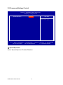
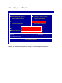
1
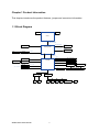
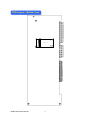
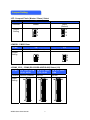
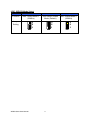
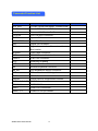
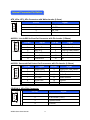
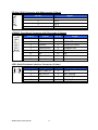
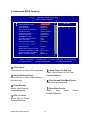
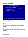
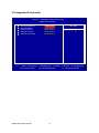
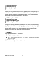
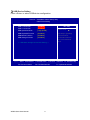
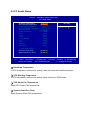
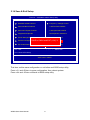
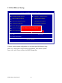
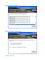
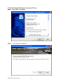
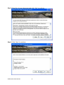
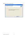
WSBC-Q450 User Manual PICMG1.0 Full-Size SBC Rev.01, Jul. 2011 Statement All rights reserved. No part of this publication may be reproduced in any form or by any means, without prior written permission of the publisher. All trademarks are the properties of the respective owners. All product specifications are subject to change without prior notice Packing List □ WSBC-Q450 □ Driver CD (Include user’s manual) Ordering Information □ □ □ □ □ 1 x PS2 Y Cable(KB and Mouse) 1 x LPT Cable with Bracket 1 x 2 Port COM Cable with Bracket 1 x 2 Port USB Cable with Bracket 1 x SATA Cable WSBC-Q450 User Manual 2 Contents Chapter 1 Product Information ........................................................................................ ..4 1.1 Block Diagram ............................................................................................................. 4 1.2 Features ........................................................................................................................ 5 1.3 PCB Layout .................................................................................................................. 7 1.4 Jumper Setting ............................................................................................................ 9 1.5 Connector Function List......................................................................................... 12 1.6 Internal Connector Pin Define............................................................................... 13 Chapter 2 BIOS Setup ........................................................................................................ 19 2.1 Main Menu .................................................................................................................. 19 2.2 Standard CMOS Features ....................................................................................... 20 2.3 Advanced BIOS Features ....................................................................................... 21 2.4 Advanced Chipset Features .................................................................................. 23 2.5 Integrated Peripherals............................................................................................. 24 2.6 Power Management Setup ..................................................................................... 32 2.7 PnP/PCI Configurations .......................................................................................... 34 2.8 PC Health Status ....................................................................................................... 35 2.9 Frequency/Voltage Control .................................................................................... 36 2.10 Load Fail-Safe Defaults......................................................................................... 37 2.11 Load Optimized Defaults ...................................................................................... 38 2.12 Set Supervisor Password .................................................................................... 39 2.13 Set User Password ................................................................................................ 40 2.14 Save & Exit Setup................................................................................................... 41 2.15 Exit Without Saving ............................................................................................... 42 Chapter 3 Drivers Installation .......................................................................................... 43 3.1 Intel Chipset Device Software ............................................................................... 43 3.2 Net Framework .......................................................................................................... 46 3.3 Intel Graphic Media Accelerator Driver .............................................................. 47 3.4 LAN Driver .................................................................................................................. 53 3.5 Audio Driver………………………………………………………..…………….....53 Appendix-A Watchdog ....................................................................................................... 54 Appendix-B GPIO ................................................................................................................ 56 WSBC-Q450 User Manual 3 Chapter 1 Product Information This chapter introduces the product features, jumper and connector information. 1.1 Block Diagram VRD11.0 CK505 Processor LGA775 FSB 800/1066/1333 MHz DDR3 800/1066 MHz VGA Channel A DDR3 240 Pin Intel Q45 (EagleLake) DDR3 800/1066 MHz Channel B DDR3 240 Pin DVI-D ASM1442T TMDS-C Pin Header DMI SATA x6 CF Jmicron_JMB368 Controller Link GLCI LCI Intel PCI-E LAN1: Intel_82567LM PCI-E ICH10DO LAN2: Intel_82574L CODEC: ALC662 / ALC888 Mini PCI-E IOx1, Pin Headerx6 PCI-E, USB PCI PCI-to-ISA (IT8888G) USB x7 SPI PICMG 1.0 Golden Finger LPC S/IO_ F81216 D COM3 COM4 S/IO_W83627EHG KB/MS PRN DIO 4 In, 4 Out WSBC-Q450 User Manual 4 COM1 COM2(RS232/422/485) IrDA IT8209 Features Intel® Core 2 Quad /Core 2 Duo/Dual-Core Processor LGA 775 SystemProcessor/ Chipsets FSB Chipset BIOS Technology Memory Display Award Dual channel DDR3 800MHz/1066 MHz Socket 2 x 240Pin DIMM Chipset Intel® Q45 GMCH integrated graphic device(GMA4500) VRAM Shared system memory up to 1GB Resolution Analog Display: Up to 2048 x 1536 Interface Ethernet Controller Interface Audio Controller Max.Data Transfer Rates CRT+DVI Dual 10/100/1000 Mbps LAN1: Intel 82567LM, LAN2: Intel 82574L High Definition Audio. Realtek ALC662 HD CODEC 300 MB/s Port 6 PCI 4 ISA 1 Expansion Slot mini-PCIe USB 2.0 COM Onboard Pin-Header Intel® Q45+ICH10DO Max. Capacity Up to 8GB DDR3 DRAM Dual Display SATA 800MHz/1066MHz/1333MHz Parallel 1 (PCIe x1 ) 6 4 (3xRS-232, 1x RS-232/422/485) 1 Compact Flash 1 WSBC-Q450 User Manual Front Panel 1 DVI 1 5 Audio Header 1(Lin In, Lin out , Mic In) DIO 4 in/ 4 out PS/2 1 (K/B and Mouse ) VGA 1 LAN 2x RJ45 Rear I/O USB 2.0 1 AT 1 ATX 1 Power Interval Programmable 1~255 sec./min. Output System reset Watchdog Timer Operating Temp. -5°C~ 60°C (23°F~ 140°F) Environment *Note1 Storage Temp. -20°C~ 80°C (-68°F~ 176°F) Relative Humidity Form Factor WSBC-Q450 User Manual Dimension (L*W) 0%~ 95% (non-condensing) PICMG 1.0 Full-Size SBC, 338mm x 122mm (13.31” x 4.8”) 6 PCB Layout – Top View USB1 LAN2 KB_MS LAN1 LPT VGA AUDIO1 KB LVDS_SEL AUDIO2 CD-IN JCOM2_CF6 COM2 SATA5 SATA4 JFRONT USB4 USB3 DIO USB2 IR JSMB AT_SEL LPC COM1 RT4 SATA6 SATA3 COM4 COM3 SATA1 SATA2 J5VSB JCOMS JIDE JCF JSPI DV1 J2 DIMM3 ATX_4PIN DIMM1 CPUFAN WOL SYSFAN ATX-2X2 ATX_12V_5V_Input WSBC-Q450 User Manual 7 PCB Layout – Bottom View MINI_PCI-E WSBC-Q450 User Manual 8 Jumper Setting JCF: Compact Flash ( Master / Slave ) Select Pin No. Function 1-2 2-3 Master Slave (Default) Jumper Setting 3 2 1 3 2 1 JCMOS1: CMOS Clear Pin No. Function 1-2 2-3 Normal Operation (Default) Jumper Setting Clear CMOS Contents 3 2 1 3 2 1 JCOM2_CFG:COM2 (RS-232/RS-422/RS-485) Select (1/2) Pin No. 5-6, 11-13, 12-14, 19-21, 20-22 Function RS-232 (Default) umper Setting 24 2 WSBC-Q450 User Manual 1 3-4, 9-11, 10-12, 1-2, 9-11, 10-12, 17-19, 18-20 23-24 RS-422 RS-485 24 23 24 23 2 1 2 1 9 JCOM2_CFG:COM2 (RS-232/RS-422/RS-485) Select (2/2) Pin No. 7-8 (Not recommended) 15-16 Function RS422 TXD Pair 100Ohm Termination Jumper Setting 7-8 RS422 RXD Pair 100Ohm Termination RS485 Data Pair 100Ohm Termination 24 23 24 23 24 23 2 1 2 1 2 1 AT_SEL: AT / ATX Mode Select Pin No. 1-2 2-3 Function AT Mode ATX Mode (Default) Jumper Setting 3 2 1 3 2 1 J5VSB: 5V connector to 5VSB Select Pin No. 1-2 2-3 Function 5V connect to 5VSB 5V not connect to 5VSB (Default) Jumper Setting WSBC-Q450 User Manual 3 2 1 3 2 1 10 JIDE: IDE ATA Mode Select Pin No. Function 1-2 2-3 All Open Max. UDMA Mode 1 (33MHz) Auto Detect UDMA Mode (Default) Min. UDMA Mode 2 (66MHz) Jumper Setting WSBC-Q450 User Manual 3 2 1 3 2 1 11 3 2 1 Connector Function List Connector Function ATX_4Pin +5VSB, PSON,GND signal , connect to BP Audio1 Line-In/MIC-In/Line-Out Connectors Audio2 Surround-Out/Center-Out Connectors CPUFAN CPU Fan 4Pin Connector SYSFAN System FAN connector COM 1/2/3/4 Serial Port Connectors DIO Digital I/O Connector DVI Digital Video Interface Connector wirh Box-header JFRONT Front Panel Connector JSPI SPI BIOS tool reflash function LAN1/2 RJ45 LAN Connector LPC Reserved for debug LPT Parallel Port Connectors KB External Keyboard Connector KB_MS PS2 Keyboard & Mouse Connector WOL PCI card wake-on LAN signal PWR ATX 2x2 connector PWR4P Power input for Single Board function SATA1, 2, 3. 4,5,6 SATA Connector DIMM1, 2 DDR3 DIMM connector USB1 USB1 Port Connectors USB2, 3, 4 USB2/3/4 Port pin header. WSBC-Q450 User Manual 12 Note Internal Connector Pin Define ATX_4Pin: ATX_4Pin Connector with Wafer-header (2.5mm) 1 Pin No. 4 Signal 1 ATX_Power OK 2 +5VSB 3 PS_ON- 4 Ground AUDIO1: Line-In/MIC-In/Line-Out Connector with Pin-header (2.54mm) 11 10 Pin No. 2 1 Signal Pin No. Signal 1 Line-In-L 2 Line-In Jack Detect 3 Line-In-R 4 MIC-In Jack Detect 5 MIC-In-L 6 Line-Out Jack Detect 7 MIC-In-R 8 Audio Ground 9 Line-Out-L 10 Audio Ground 11 Line-Out-R 12 NC AUDIO2: Surround-Out/Center-Out Connectors with Pin-header (2.54mm) 11 10 2 1 Pin No. Signal Pin No. Signal 1 SURR-Out-L 2 SURR-Out Jack Detect 3 SURR-Out-R 4 CEN-Out Jack Detect 5 CEN-Out 6 Audio Ground 7 LEF-Out 8 Audio Ground 9 SPDIF-Out 10 Ground 11 +5V 12 NC CPUFAN: 4Pin FAN Connector 1 4 WSBC-Q450 User Manual Pin No. Signal 1 Ground 2 Fan Power (+12V) 3 Speed Sense 4 Control 13 SYSFAN: System FAN connector 3 Pin No. 1 Signal 1 Sense 2 +12V 3 Ground COM1/COM2/COM3/COM4: Serial Port with Box-header (2.54mm) 9 8 2 1 Pin No. Signal Pin No. Signal 1 DCD 2 DSR 3 RXD 4 RTS 5 TXD 6 CTS 7 DTR 8 RI/+5V/+12V 9 Ground 10 NC DIO: Digital I/O Connector with Pin-header (2.54mm) 11 10 2 1 Pin No. Signal Pin No. Signal 1 DIO-Out0 2 DIO-In0 3 DIO-Out1 4 DIO-In1 5 DIO-Out2 6 DIO-In2 7 DIO-Out3 8 DIO-In3 9 +12V 10 +5V 11 Ground 12 NC DVI: Digital Video Interface with Box-header (1.0 mm) 2 20 Pin No. 1 19 Signal Pin No. Signal 1 HDMI_TX0+ 2 HDMI_TXC+ 3 HDMI_TX0- 4 HDMI_TXC- 5 Ground 6 Ground 7 HDMI_TX1+ 8 L_DDC_SC 9 HDMI_TX1- 10 L_DDC_SD 11 Ground 12 Ground 13 HDMI_TX2+ 14 HDMI_HPD 15 HDMI_TX2- 16 DVI_5V 17 Ground 18 Ground 19 Ground 20 Ground WSBC-Q450 User Manual 14 CD-IN:CD-IN Connector with Wafer-header (2.5mm) 4 Pin No. 1 Signal 1 CD-L 2 CD-G 3 CD-G 4 CD-R JFRONT: Front Panel Connector with Pin-header (2.54mm) 15 2 1 Pin No. Signal Pin No. Signal 1 +5V (470 Ohm) 2 +5V (470 Ohm) 3 NC 4 HDD LED 5 Ground 6 5VSB (470 Ohm) 7 Reset Switch 8 Suspend LED 9 Ground 10 Speaker 11 NC 12 NC 13 Power Switch 14 NC 15 Ground 16 +5V JSPI: Serial Peripheral Interface Connector (2.0mm) 2 8 1 7 Pin No. Signal Pin No. 1 SPI_CS#0_R 2 +3.3V 3 SPI_SO_R 4 SPI_HOLD# 5 NC 6 SPI_CLK_R 7 Ground 8 SPI_SI_R WSBC-Q450 User Manual 15 Signal LPT:Parallel Port Connector with Box-header (2.54mm) Pin No. Signal Pin No. Signal 1 Strobe# 14 Auto Form Feed# 2 Data 0 15 Error# 3 Data 1 16 Initialization# 4 Data 2 17 Printer Select IN# 5 Data 3 18 Ground 6 Data 4 19 Ground 7 Data 5 20 Ground 8 Data 6 21 Ground 9 Data 7 22 Ground 10 Acknowledge# 23 Ground 11 Busy 24 Ground 12 Paper Empty 25 Ground 13 Printer Select 26 Ground KB:External Keyboard Connector with Wafer-header (2.5mm) Pin No. Signal 1 KBCLK 2 KBDATA 3 NC 4 Ground 5 +5V KB_MS:PS2 Keyboard & Mouse with Mini-DIN Connector Pin No. Signal Pin No. Signal 1 KBDATA 2 MSDATA 3 Ground 4 +5V 5 KBCLK 6 MSCLK WOL: PCI card wake-on LAN signal (2.0mm) Pin No. Signal 1 +5V 2 Ground 3 PCI_PME# WSBC-Q450 User Manual 16 PWR:ATX 2x2 Power Connector (4.2mm) Pin No. Signal 1 Ground 2 Ground 3 +12V DC-In 4 +12V DC-In ATX_12V_5V_Inpput: Power input for Single Board function (4.2mm) Pin No. Signal 1 +5V 2 Ground 3 Ground 4 +12V USB1:USB1 for IO connector Pin No. Signal 1 USB Power (+5V) 2 USB DATA0- 3 USB DATA0+ 4 USB Ground USB2/3/4: USB2/3/4 Port Connector with Wafer-header (2.5mm) Pin No. Signal Pin No. Signal 1 USB Power (+5V) 2 USB Power (+5V) 3 USB DATA- 4 USB DATA- 5 USB DATA+ 6 USB DATA+ 7 USB Ground 8 USB Ground 9 NC 10 Case Ground ATX_4Pin: ATX_4Pin Connector with Wafer-header (2.5mm) Pin No. Signal 1 ATX_Power OK 2 +5VSB 3 PS_ON- 4 Ground WSBC-Q450 User Manual 17 IR: IR Connector with Wafer-header (2.5mm) Pin No. Signal 1 +5V 2 NC 3 SINB 4 Ground 5 SOUTB LPC: LPC Connector with Wafer-header (2.0mm) Pin No. Signal 1 LAD0 2 PLTRST- 3 LAD1 4 LFRAME# 5 LAD2 6 +3.3V 7 LAD3 8 Ground 9 CLK_LPC3_33M 10 NC WSBC-Q450 User Manual 18 Chapter 2 BIOS Setup This chapter introduces BIOS setup information. Power on or reboot the system board, when screen appears message as “Press DEL to enter SETUP“. Press <DEL> key to run BIOS SETUP Utility. Note: The BIOS configuration for reference only, it may subject to change without prior notice. 2.1 Main Menu Please use arrow keys to select item, then press <Enter> key to accept or enter the sub-menu. Phoenix – AwardBIOS CMOS Setup Utility Standard CMOS Features Frequency / Voltage Control Advanced BIOS Features Load Fail-Safe Defaults Advanced Chipset Features Load Optimized Defaults Integrated Peripherals Set Supervisor Password Power Management Setup Set User Password PnP/PCI Configurations Save & Exit Setup PC Health Status Exit Without Saving ↑↓ ← → : Select Item Esc : Quit F10 : Save & Exit Setup Time, Date, Hard Disk Type… WSBC-Q450 User Manual 19 2.2 Standard CMOS Features Phoenix – AwardBIOS CMOS Setup Utility Standard CMOS Features Date (mm:dd:yy) Time (hh:mm:ss) Item Help Mon. Jul. 11 2011 11 : 28 : 10 Menu Level IDE Channel 0 Master IDE Channel 0 Slave IDE Channel 2 Master IDE Channel 2 Slave IDE Channel 3 Master [ [ [ [ [ Video Halt On [ EGA / VGA ] [ All , But Keyboard ] Base Memory Extended Memory Total Memory ↑↓→ ← :Move Enter:Select F5: Previous Values None ] None ] None ] None ] None ] Change the day, month, year and century 639K 1011712K 1012736K +/-/PU/PD:Value F10:Save F6: Fail-Safe Defaults ESC:Exit F1: General Help F7: Optimized Defaults □ Date □ IDE Channel 3 Master Set system date. Press <Enter> for IDE device automatic detection. □ Time □ Video Set system time. Select Video device type. □ IDE Channel 0 Master/Slave □ Halt on Press <Enter> for IDE device automatic detection. Select stop procedure or ignore when error detected during POST (Power On Self Test). □ IDE Channel 2 Master/Slave Press <Enter> for IDE device automatic detection. WSBC-Q450 User Manual 20 2.3 Advanced BIOS Features Phoenix – AwardBIOS CMOS Setup Utility Advanced BIOS Features CPU Feature Hard Disk Boot Priority Virus Warning CPU L3 Cache Quick Power On Self Test First Boot Device Second Boot Device Third Boot Device Boot Other Device Boot Up NumLock Status Gate A20 Option Typematic Rate Setting X Typematic Rate (Chars/Sec) X Typematic Delay (Msec) Security Option MPS Version Control For OS Os Select For DRAM > 64MB Report No FDD For WIN 95 Small Logo(EPA) Show ↑↓→ ← :Move Enter:Select F5: Previous Values [ Press Enter ] [ Press Enter ] [ Disabled ] [ Enabled ] [ Enabled ] [ USB-CDROM ] [ Hard Disk ] [ USB-FDD ] [ Enabled ] [ Off ] [ Fast ] [ Disabled ] 6 250 [ Setup ] [ 1.4 ] [ Non-OS2 ] [ No ] [ Disabled ] +/-/PU/PD:Value ▲ Menu Level ▼ F10:Save F6: Fail-Safe Defaults Item Help ESC:Exit F1: General Help F7: Optimized Defaults □ CPU Feature Press <Enter> to select CPU parameter. □ Quick Power On Self Test □ Hard Disk Boot Priority Select “Quick Power On Self Test” Enabled/Disabled. Press <Enter> to select Hard Disk boot device priority. □ First/Second/Third Boot Device Select boot device priority. □ Virus Warning □ Boot Other Device Select “Virus Warning” Enabled/Disabled. Select “Boot Enabled/Disabled. □ CPU L3 Cache Select “CPU L3 Cache” Enabled/Disabled. WSBC-Q450 User Manual 21 Other Device” □ Boot Up NumLock Status □ OS Select For DRAM > 64M Select <NumLock> key ON/Off when system boot up. Select “OS2” only if you are running older version of IBM OS/2 Operating System with greater than 64MB of RAM on the system. Otherwise select “Non-OS/2” setting. □ Gate A20 Option Select Gate A20 controlled by Keyboard controller (Normal) or Port 92 (Fast). □ Report No FDD For WIN 95 □ Typematic Rate Setting If running Windows 95/98 without floppy diskdrive, select “Enabled” to release IRQ6. This is required to pass Windows 95/98's SCT test, If select “Disabled”, BIOS will not report missing floppy drive to Win95/98. Select “Typematic Rate Setting” Enabled to set, Typematic Rate (Chars/Sec): Number of characters repeated in one second. Typematic Delay (Msec): When holding one key, set the time between the first and second character displayed. □ Small Logo(EPA) Show Select EPA (Environmental Protection Agency) Energy Star logo appears during the system boot-up process. □ Security Option Select security mode, Setup: Require password to permit BIOS setup utility. System: Require password to permit boot-up and BIOS setup utility. □ MPS Version Control For OS Select MPS (Multiprocessor Specification) Version 1.4 to added extended configuration tables to improve support for multiple PCI bus configurations and improve future expandability. It is also required for a secondary PCI bus to work without the need for a bridge. Select Version 1.1 for older Operating Systems. WSBC-Q450 User Manual 22 2.4 Advanced Chipset Features Phoenix – AwardBIOS CMOS Setup Utility Advanced Chipset Features PCI Express Root Port Func Port 80h to ** VGA Setting ** On-Chip Frame Buffer Size DVMT Mode Total GFX Memory ↑↓→ ← :Move Enter:Select F5: Previous Values [ Press Enter ] [PCI] Item Help Menu Level [ 32MB ] [ Enabled ] [ 128MB ] +/-/PU/PD:Value F10:Save F6: Fail-Safe Defaults ESC:Exit F1: General Help F7: Optimized Defaults □ On-Chip Frame Buffer Size Select share system memory 1MB or 8MB. □ DVMT Mode DVMT (Dynamic Video Memory Technology) allowing the system to dynamically allocate memory resources according to the demands of the system at any point in time, that improve efficiency of the memory allocated to either system or graphics processor. □ Total GFX Memory Select Total GFX Memory: 128MB, 256MB, or MAX. (For Win XP, the MAX Value is base on system memory size, 512MB for 1GB DRAM, 768MB for 1.5GB to 2GB, 1GB fro above 2GB.) WSBC-Q450 User Manual 23 2.5 Integrated Peripherals Phoenix – AwardBIOS CMOS Setup Utility Integrated Peripherals OnChip IDE Device Onboard Device Super IO Device SecondIO Device USB Device Setting ↑↓→ ← :Move Enter:Select F5: Previous Values WSBC-Q450 User Manual [ Press Enter ] [ Press Enter ] [ Press Enter ] [ Press Enter ] [ Press Enter ] +/-/PU/PD:Value F10:Save F6: Fail-Safe Defaults 24 Item Help Menu Level ESC:Exit F1: General Help F7: Optimized Defaults □ OnChip IDE Device Press <Enter> to set IDE and SATA device configuration. Phoenix – AwardBIOS CMOS Setup Utility OnChip IDE Device IDE HDD Block Mode IDE DMA transfer access IDE Primary Master PIO IDE Primary Slave PIO IDE Primary Master UDMA IDE Primary Slave UDMA On-chip Secondary PCI IDE IDE Secondary Master PIO IDE Secondary Slave PIO IDE Secondary Master UDMA IDE Secondary Slave UDMA SATA Mode LEGACY Mode Support ↑↓→ ← :Move Enter:Select F5: Previous Values [ Enabled ] [ Enabled ] [ Auto ] [ Auto ] [ Auto ] [ Auto ] [ Enabled ] [ Auto ] [ Auto ] [ Auto ] [ Auto ] [ IDE ] [ Enabled ] +/-/PU/PD:Value F10:Save F6: Fail-Safe Defaults Item Help Menu Level If your IDE hard drive supports block mode select Enabled for automatic detection of the optimal number of block read/writes per sector the drive can support ESC:Exit F1: General Help F7: Optimized Defaults □ IDE HDD Block Mode Block mode is also called block transfer, multiple commands, or multiple sector read/write. □ IDE DMA transfer access UDMA (Ultra DMA) is a DMA data transfer protocol that utilizes ATA commands and the ATA bus to allow DMA commands to transfer data at a maximum burst rate of 33 MB/s. □ On-Chip Secondary PCI IDE The chipset contains a PCI IDE interface with support for two IDE channels. Select Enabled to activate the IDE interface. Select Disabled to deactivate this interface, if you install a primary and/or secondary add-in IDE interface. WSBC-Q450 User Manual 25 □ □ □ □ IDE Primary Master PIO IDE Primary Slave PIO Secondary Master PIO Secondary Slave PIO The four IDE PIO (Programmed Input/Output) fields let you set a PIOmode (0-4) for each of the four IDE devices that the onboard IDE interface supports. Modes 0 through 4 provide successively increased performance. In Auto mode, the system automatically determines the best mode for each device. □ □ □ □ IDE Primary Master UDMA IDE Primary Slave UDMA IDE Secondary Master UDMA IDE Secondary Slave UDMA UDMA (Ultra DMA) is a DMA data transfer protocol that utilizes ATA commands and the ATA bus to allow DMA commands to transfer data at a maximum burst rate of 33 MB/s. When you select Auto in the four IDE UDMA fields (for each of up to four IDE devices that the internal PCI IDE interface supports), the system automatically determines the optimal data transfer rate for each IDE device. □ SATA Mode There have three selections in “SATA mode”: IDE: Default RAID: Enable SATA RAID function AHCI: Set this item to enable SATA AHCI function for WinXP-SPI+IAA driver support AHCI mode. □ LEGACY Mode Support Certain os is not supported under Native mode. WSBC-Q450 User Manual 26 □ Onboard Device Phoenix – AwardBIOS CMOS Setup Utility Onboard Device Onboard Lan Boot ROM ADO Control [ Disabled ] [ Enabled ] Item Help Menu Level Decide whether to invoke the boot ROM of the onboard LAN chip ↑↓→ ← :Move Enter: Select +/-/PU/PD: Value F5: Previous Values F10: Save F6: Fail-Safe Defaults ESC: Exit F7: Optimized Defaults □ Onboard Lan Boot ROM Decide whether to invoke the boot ROM of the onboard LAN chip □ ADO Control Enable/Disable Audio control. WSBC-Q450 User Manual 27 F1: General Help □ Super IO Device Press <Enter> to select Serial, Parallel and “l” configuration. Phoenix – AwardBIOS CMOS Setup Utility Super IO Device Onboard Serial Port 1 Onboard Serial Port 2 UART Mode Select x RxD, TxD Active x IR Transmission Delay x UR2 Duplex Mode x Use IR Pins Onboard Parallel Port Parallel Port Mode x EPP Mode Select x EPC Mode Use DMA Watchdog Timer Select ↑↓→ ← :Move Enter:Select F5: Previous Values [ 3F8/IRQ4 ] [ 2F8/IRQ3 ] [ Normal ] Hi, Lo Enabled Half IR-Rx2Tx2 [ 378/IRQ7 ] [ SPP ] EPP1.7 3 Item Help Menu Level [ Disabled ] +/-/PU/PD:Value F10:Save F6: Fail-Safe Defaults ESC:Exit F1: General Help F7: Optimized Defaults □ Onboard Serial Port 1 Select serial port 1 address: Disabled, 3F8/IRQ4, 2F8/IRQ3, 3E8/IRQ4, 2E8/IRQ3, or Auto. □ Onboard Serial Port 2 Select serial port 2 address: Disabled, 3F8/IRQ4, 2F8/IRQ3, 3E8/IRQ4, 2E8/IRQ3, or Auto. □ UART Mode Select Select UART Mode: IrDA, ASKIR, or Normal. □ Onboard Parallel Port Select onboard parallel port: Disabled, 378/IRQ7, 278/IRQ5, or 3BC/IRQ7. WSBC-Q450 User Manual 28 □ Parallel Port Mode Select Parellel Port Mode: SPP, EPP, ECP, ECP+EPP, or Normal. □ Watchdog Timer Select Select Watch dog Disabled or set timer value: 10sec, 20sec, 30sec, 40sec, 1 min, 2min, or 4min. WSBC-Q450 User Manual 29 □ Second IO Device Phoenix – AwardBIOS CMOS Setup Utility Second IO Device Onboard Serial Port 3 [ 3E8h ] Onboard Serial Port 4 [ 2E8h ] Item Help Menu Level ↑↓→ ← :Move Enter:Select F5: Previous Values +/-/PU/PD:Value F6: Fail-Safe Defaults □ Onboard Serial Port 3/4 Select serial port address. WSBC-Q450 User Manual F10:Save 30 ESC:Exit F1: General Help F7: Optimized Defaults □ USB Device Setting Press <Enter> to select USB device configuration. Phoenix – AwardBIOS CMOS Setup Utility USB Device Setting USB 1.0 Controller [ Enabled ] USB 2.0 Controller [ Enabled ] USB Operation Mode [ High Speed ] USB Keyboard Function [ Enabled ] USB Mouse Function [ Enabled ] USB Storage Function [ Enabled ] Item Help Menu Level *** USB Mass Storage Device Boot Setting *** ↑↓→ ← :Move Enter:Select F5: Previous Values WSBC-Q450 User Manual +/-/PU/PD:Value F10:Save F6: Fail-Safe Defaults 31 [Enable] or [Disable] Universal Host Controller Interface for Universal Serial Bus. ESC:Exit F1: General Help F7: Optimized Defaults 2.6 Power Management Setup Phoenix – AwardBIOS CMOS Setup Utility Power Management Setup x x ACPI Function ACPI Suspend Type Soft-Off by PWR-BTTN Wake-Up by PCI card Power On by Ring Resume by Alarm Date (of Month) Alarm Time (hh:mm:ss) Alarm PCI Express PM Function ↑↓→ ← :Move Enter:Select F5: Previous Values [ Enabled ] [ S1(POS) ] [ Instant-Off ] [ Disabled ] [ Disabled ] [ Disabled ] 0 0 : 0 : 0 [ Press Enter ] +/-/PU/PD:Value F10:Save F6: Fail-Safe Defaults Item Help Menu Level ESC:Exit F1: General Help F7: Optimized Defaults □ ACPI Function Select ACPI (Advanced Configuration and Power Management) Enabled/Disabled. □ ACPI Suspend Type Select S1(POS) type. □ Soft-Off by PER-BTTN Select power button function, Instant-off: Press power button will power off instantly. Delay 4 Sec: Press power button 4 second to power off. □ Wake-Up by PCI card Select Wake-UP by PCI device Enabled/Disabled □ Power On by Ring Select Power on by Ring Indicator signal from Modem. WSBC-Q450 User Manual 32 □ Resume by Alarm Set date and time to power on system from soft-off state. □ PCI Express PM Function Press <Enter> to select “Wake-up by LAN” Enabled/Disabled. Phoenix – AwardBIOS CMOS Setup Utility PCI Express PM Function Wake-up by Lan [ Disabled ] Item Help Menu Level ↑↓→ ← :Move Enter:Select F5: Previous Values +/-/PU/PD:Value F6: Fail-Safe Defaults □ Wake-up by Lan Select wake-up by Lan Enabled/Disabled. WSBC-Q450 User Manual F10:Save 33 ESC:Exit F1: General Help F7: Optimized Defaults 2.7 PnP/PCI Configurations Phoenix – AwardBIOS CMOS Setup Utility PnP / PCI Configurations x Item Help PNP OS Installed Init Display First Reset Configuration Data [ No ] [ PCI Slot ] [ Disabled ] Resources Controlled By IRQ Resources DMA Resources [ Auto (ESCD) ] Press Enter Press Enter PCI/VGA Palette Snoop [ Disabled ] Menu Level Select Yes if you are using a Plug and Play capable operating system Select No if you need the BIOS to configure non-boot devices ** PCI Express relative items ** Maximum Payload Size [ 128 ] ↑↓→ ← :Move Enter:Select F5: Previous Values +/-/PU/PD:Value F10:Save F6: Fail-Safe Defaults ESC:Exit F1: General Help F7: Optimized Defaults □ Init Display First □ Resources Controlled By Select initial display by PCI or Onboard device. BIOS can automatically configure all the boot and Plug and Play compatible devices. If you choose Auto, you cannot select IRQ DMA and memory base address fields, since BIOS automatically assigns them. □ Reset Configuration Data Select Enabled to reset Extended System Configuration Data (ESCD) when you exit BIOS setup utility, if you have installed new add-on card and the system reconfiguration has caused such a serious conflict that the OS cannot boot. □ PCI/VGA Palette Snoop Select PCI/VGA Palette Snoop Enabled/Disabled. □ Maximum Payload Size Set maximum TLP payload size for the PCI Express devices. The unit is byte. WSBC-Q450 User Manual 34 2.8 PC Health Status Phoenix – AwardBIOS CMOS Setup Utility PC Health Status [ Disabled ] Shutdown Temperature [ Disabled ] CPU Warning Temperature Current CPU Temperature 40°C/ 104°F Current SYSTEM Temperature 47°C/ 116°F CPU Fan Speed 2109 RPM System Fan Speed 0 RPM Vcore 1.24 V +12 V 12.09 V +1.5 V 1.47 V +1.5 V (DRAM) 1.46 V +5 V 5.00 V +3.3 V 3.34 V VBAT (V) 3.04 V 3.3VSB (V) 3.34 V ** Smart FAN Setting ** CPU Smart Fan Temp. System Smart Fan Temp. ↑↓→ ← :Move Enter:Select F5: Previous Values Item Help Menu Level [ Disabled ] [ Disabled ] +/-/PU/PD:Value F10:Save F6: Fail-Safe Defaults ESC:Exit F1: General Help F7: Optimized Defaults □ Shutdown Temperature If CPU temperature reaches the setting value will automatic shutdown system. □ CPU Warning Temperature If CPU temperature reaches the setting value will beep in DOS mode. □ CPU Smart Fan Temperature Setup CPU Smart FAN temperature. □ System Smart Fan Temp. Setup System Smart FAN temperature. 2.9 Frequency/Voltage Control Phoenix – AwardBIOS CMOS Setup Utility Frequency / Voltage Control Spread Spectrum [ Disabled ] Item Help Menu Level ↑↓→ ← :Move Enter:Select F5: Previous Values +/-/PU/PD:Value F6: Fail-Safe Defaults □ Spread Spectrum Select “Spread Spectrum” Enabled/Disabled. WSBC-Q450 User Manual F10:Save 36 ESC:Exit F1: General Help F7: Optimized Defaults 2.10 Load Fail-Safe Defaults Phoenix – AwardBIOS CMOS Setup Utility Standard CMOS Features Frequency / Voltage Control Advanced BIOS Features Load Fail-Safe Defaults Advanced Chipset Features Load Optimized Defaults Integrated Peripherals Set Supervisor Password Power Management Setup Set User Password PnP/PCI Configurations & Exit Load Fail-Safe Defaults Save (Y/N)? N Setup Load Fail-Safe Defaults (Y/N)? N PC Health Status Exit Without Saving ↑↓ ← → : Select Item Esc : Quit F10 : Save & Exit Setup Load Fail-Safe Defaults This item will set configuration for non-optimized system operation. WSBC-Q450 User Manual 37 2.11 Load Optimized Defaults Phoenix – AwardBIOS CMOS Setup Utility Standard CMOS Features Frequency / Voltage Control Advanced BIOS Features Load Fail-Safe Defaults Advanced Chipset Features Load Optimized Defaults Integrated Peripherals Set Supervisor Password Power Management Setup Set User Password PnP/PCI Configurations & Exit Load Optimized DefaultsSave (Y/N)? N Setup Load Optimized Defaults (Y/N)? N PC Health Status Exit Without Saving ↑↓ ← → : Select Item Esc : Quit F10 : Save & Exit Setup Load Optimized Defaults This item will restore factory default setting for optimized system operation. WSBC-Q450 User Manual 38 2.12 Set Supervisor Password Phoenix – AwardBIOS CMOS Setup Utility Standard CMOS Features Frequency / Voltage Control Advanced BIOS Features Load Fail-Safe Defaults Advanced Chipset Features Load Optimized Defaults Integrated Peripherals Set Supervisor Password Power Management Setup Set User Password PnP/PCI Configurations Save & Exit Setup Enter Password: PC Health Status Exit Without Saving ↑↓ ← → : Select Item Esc : Quit F10 : Save & Exit Setup Change/Set/Disabled Password If set supervisor password, it will request typing password to enter BIOS setup utility. WSBC-Q450 User Manual 39 2.13 Set User Password Phoenix – AwardBIOS CMOS Setup Utility Standard CMOS Features Frequency / Voltage Control Advanced BIOS Features Load Fail-Safe Defaults Advanced Chipset Features Load Optimized Defaults Integrated Peripherals Set Supervisor Password Power Management Setup Set User Password PnP/PCI Configurations Save & Exit Setup Enter Password: PC Health Status Exit Without Saving ↑↓ ← → : Select Item Esc : Quit F10 : Save & Exit Setup Change/Set/Disabled Password If set user password will request typing password to enter BIOS setup utility, and does not allow modifying configuration. WSBC-Q450 User Manual 40 2.14 Save & Exit Setup Phoenix – AwardBIOS CMOS Setup Utility Standard CMOS Features Frequency / Voltage Control Advanced BIOS Features Load Fail-Safe Defaults Advanced Chipset Features Load Optimized Defaults Integrated Peripherals Set Supervisor Password Power Management Setup Set User Password PnP/PCI Configurations Save & ExitYSetup SAVE to CMOS and EXIT (Y/N)? SAVE to CMOS and EXIT (Y/N)? Y PC Health Status Exit Without Saving ↑↓ ← → : Select Item Esc : Quit F10 : Save & Exit Setup Save Data to CMOS This item confirm save configuration or not before exit BIOS setup utility, Press <Y> and <Enter> to save configuration, then reboot system. Press <N> and <Enter> will back to BIOS setup utility. WSBC-Q450 User Manual 41 2.15 Exit Without Saving Phoenix – AwardBIOS CMOS Setup Utility Standard CMOS Features Frequency / Voltage Control Advanced BIOS Features Load Fail-Safe Defaults Advanced Chipset Features Load Optimized Defaults Integrated Peripherals Set Supervisor Password Power Management Setup Set User Password PnP/PCI Configurations Save &NExit Setup Quit Without Saving (Y/N)? Quit Without Saving (Y/N)? N PC Health Status Exit Without Saving ↑↓ ← → : Select Item Esc : Quit F10 : Save & Exit Setup Abandon all Data This item confirm save configuration or not before quit BIOS setup utility, Press <Y> and <Enter> will not save configuration, then reboot system. Press <N> and <Enter> will back to BIOS setup utility. WSBC-Q450 User Manual 42 Chapter 3 Drivers Installation This chapter introduces driver installation information. Please insert the utility CD to CD-ROM drive, the install menu will appear automatically, if the install menu did not list suitable driver of Operate System or did not appear automatically, please select corresponding driver of utility CD to install. The Windows XP driver installation steps are as below. 3.1 Intel Chipset Device Software Step 1. Click “Next” to continue. WSBC-Q450 User Manual 43 Step 2. Read the License Agreement and click “Yes” to continue. Step 3. Click “Next” to continue. WSBC-Q450 User Manual 44 Step 4. Click “Next” to continue. Step 5. Click “Finish” to complete setup. WSBC-Q450 User Manual 45 3.2 Net Framework Step 1. Click “Install” to continue. Step 2. Click “Exit” to complete setup. WSBC-Q450 User Manual 46 3.3 Intel Graphic Media Accelerator Driver Step 1. Click “Next” to continue. Step 2. Click “Next” to continue. WSBC-Q450 User Manual 47 Step 4. Read the License Agreement and click “Yes” to continue. Step 5. Click “Next” to continue. WSBC-Q450 User Manual 48 Step 6. Click “Next” to continue. Step 7. Click “Finish” to complete setup. WSBC-Q450 User Manual 49 3.4 LAN Driver Step 1. Click “Next” to continue Step 2. Click “Next” to continue WSBC-Q450 User Manual 50 Step 3. Click “Next” to continue Step 4. Click “Install” to continue WSBC-Q450 User Manual 51 Step 5. Click “Finish” to complete setup. WSBC-Q450 User Manual 52 3.5 Audio Driver Step 1. Click “Next” to continue Step 2. Click “Finish” to complete setup. WSBC-Q450 User Manual 53 Appendix-A Watchdog The working algorithm of the WDT function can be simply described as a counting process. The Time-Out Interval can be set through software programming. The availability of the time-out interval settings by software. The System Board allows users control WDT through dynamic software programming. The WDT starts counting when it is activated. It sends out a signal to system reset, when time-out interval ends. To prevent the time-out interval from running out, a re-trigger signal will need to be sent before the counting reaches its end. This action will restart the counting process. WDT program should keep the counting process running under normal condition. WDT should never generate a system reset unless the system runs into troubles. The related Control Registers of WDT are all included in the following sample program that is written in C language. User can fill a non-zero value into the Time-out Value Register to enable/refresh WDT. System will be reset after the Time-out Value to be counted down to zero. Or user can directly fill a zero value into Time-out Value Register to disable WDT immediately. To ensure a successful accessing to the content of desired Control Register, the sequence of following program codes should be step-by-step run again when each register is accessed. For more information about WDT, please refer to Winbond W83627EHF data sheet. There are two PnP I/O port addresses that can be used to configure WDT, 1) 0x2E:EFIR (Extended Function Index Register, for identifying CR index number) 2) 0x2F:EFDR (Extended Function Data Register, for accessing desired CR) Below are some example codes, which demonstrate the use of WDT. WSBC-Q450 User Manual 54 // Enter Extended Function Mode outp(0x002E, 0x87); outp(0x002E, 0x87); // Assign Pin 77 to be a WDTO# Signal outp(0x002E, 0x2D); outp(0x002F, inp(0x002F) & 0xFE); // Select Logic Device 8 outp(0x002E, 0x07); outp(0x002F, 0x08); // Active Logic Device 8 outp(0x002E, 0x30); outp(0x002F, 0x01); //Clear WDTO# Status outp(0x002E, 0xF7); outp(0x002F, inp(0x2F) & 0xEF); // Select Count Mode (Second / Minute) outp(0x002E, 0xF5); outp(0x002F, (inp(0x002F) & 0xF7) | ( Count-mode Register // Set Time-out Value outp(0x002E, 0xF6); outp(0x002F, Time-out Value Register ); // Exit Extended Function Mode outp(0x002E, 0xAA); Definitions of Variables: Value of Count-mode Register : 1) 0x00 -- Count down in seconds (Bit3=0) 2) 0x08 -- Count down in minutes (Bit3=1) Value of Time-out Value Register : 1) 0x00 -- Time-out Disable 2) 0x01~0xFF -- Value for counting down WSBC-Q450 User Manual 55 & 0x08)); Appendix-B GPIO The System Board provides 4 dedicated output ports and 4 programmable I/O ports that can be individually configured to perform a simple I/O function. Users can configure 4 programmable I/O ports to become an input or output port by programming register bit of I/O Selection .To invert port value, the setting of Inversion Register has to be made(Note). Port values can be set to read or write through Data Register. Note : Only 4 programmable I/O ports support. Additionally, 4 Digital Output ports amplified signals from GPIO ports. There are open-drain buffers, which can offer greater driving capacity up to 100mA. For more information about GPIO, please refer to Winbond W83627EHF data sheet. The related Control Registers of GPIO are all included in the following sample program that is written in C language. To ensure a successful accessing to the content of desired Control Register, the sequence of following program codes should be step-by-step run again when each register is accessed. There are two PnP I/O port addresses that can be used to configure GPIO ports, 1) 0x2E - EFER (Extended Function Enable Register, for entering Extended Function Mode) - EFIR (Extended Function Index Register, for identifying CR index number) 2) 0x2F - EFDR (Extended Function Data Register, for accessing desired CR) Below are some example codes, which demonstrate the use of GPIOs. // Enter Extended Function Mode outp(0x002E, 0x87); outp(0x002E, 0x87); // Assign Pin121-128 to be GPIO port outp(0x002E, 0x29); outp(0x002F, inp(0x002F) | 0x01); WSBC-Q450 User Manual 56 // Select Logic Device 7 outp(0x002E, 0x07); outp(0x002F, 0x07); // Active Logic Device 7 outp(0x002E, 0x30); outp(0x002F, 0x01); // Select Inversion Mode outp(0x002E, 0xF2); outp(0x002F, (inp(0x002F) & 0x3C) | ( Inversion Register & 0xC3)); // Select I/O Mode outp(0x002E, 0xF0); outp(0x002F, (inp(0x002F) & 0x3C) | ( I/O Selection Register // Access GPIO ports outp(0x002E, 0xF1); outp(0x002F, (inp(0x002F) & 0x3C) | ( Output Data or Input Data = inp(0x002F); & 0xC3)); & 0xC3)); // Exit Extended Function Mode outp(0x002E, 0xAA); Definitions of Variables: Each bit in the lower nibble of each Register represents the setting of a GPIO port. Super IO Pin Bit 128 0 GPIO DIO-Out0 127 1 GPIO DIO-Out1 126 2 GPIO DIO-In0 125 3 GPIO DIO-In1 124 4 GPIO DIO-In2 123 5 GPIO DIO-In3 122 6 GPIO DIO-Out2 121 7 GPIO DIO-Out3 WSBC-Q450 User Manual 57 GPIO DIO Value of Inversion Register : When set to a ‘1’, the incoming/outgoing port value is inverted. When set to a ‘0’, the incoming/outgoing port value is the same as in Data Register. Value of I/O Selection Register : When set to a ‘1’, respective GPIO port is programmed as an input port. When set to a ‘0’, respective GPIO port is programmed as an output port. Value of Output Data / Input Data : If a port is assigned to be an output port, then its respective bit can be read/written. If a port is assigned to be an input port, then its respective bit can be read only. Note : DIO_IN0/DIO_IN1/DIO_IN2/DIO_IN3 are programmed as Inputs by BIOS default. Parameter Conditions VinH min +1.857V VinL max +0.525V Rated Vin -8V ~ +12V NC Status High by Default ** Attention : If DIO_IN0/DIO_IN1/DIO_IN2/DIO_IN3 are programmed as Output signal, they can only offer a normal signal transfer.(NOT amplified signals.) Parameter Conditions VoutH 3.3V thru 10k VoutL 0V thru 1k DIO_OUT0/DIO_OUT1/DIO_OUT2/DIO_OUT3 are fixed as Outputs by BIOS. Parameter Conditions Open-drain buffer Power-on default = Open Driving Capacity max 100mA continue WSBC-Q450 User Manual 58