1
LogiCORE™
FIFO Generator v3.3
User Guide
UG175 April 2, 2007
R
R
Xilinx is disclosing this Document and Intellectual Property (hereinafter “the Design”) to you for use in the development of designs
to operate on, or interface with Xilinx FPGAs. Except as stated herein, none of the Design may be copied, reproduced,
distributed, republished, downloaded, displayed, posted, or transmitted in any form or by any means including, but not limited to,
electronic, mechanical, photocopying, recording, or otherwise, without the prior written consent of Xilinx. Any unauthorized use
of the Design may violate copyright laws, trademark laws, the laws of privacy and publicity, and communications regulations and
statutes.
Xilinx does not assume any liability arising out of the application or use of the Design; nor does Xilinx convey any license under
its patents, copyrights, or any rights of others. You are responsible for obtaining any rights you may require for your use or
implementation of the Design. Xilinx reserves the right to make changes, at any time, to the Design as deemed desirable in the
sole discretion of Xilinx. Xilinx assumes no obligation to correct any errors contained herein or to advise you of any correction if
such be made. Xilinx will not assume any liability for the accuracy or correctness of any engineering or technical support or
assistance provided to you in connection with the Design.
THE DESIGN IS PROVIDED “AS IS” WITH ALL FAULTS, AND THE ENTIRE RISK AS TO ITS FUNCTION AND
IMPLEMENTATION IS WITH YOU. YOU ACKNOWLEDGE AND AGREE THAT YOU HAVE NOT RELIED ON ANY ORAL OR
WRITTEN INFORMATION OR ADVICE, WHETHER GIVEN BY XILINX, OR ITS AGENTS OR EMPLOYEES. XILINX MAKES
NO OTHER WARRANTIES, WHETHER EXPRESS, IMPLIED, OR STATUTORY, REGARDING THE DESIGN, INCLUDING ANY
WARRANTIES OF MERCHANTABILITY, FITNESS FOR A PARTICULAR PURPOSE, TITLE, AND NONINFRINGEMENT OF
THIRD-PARTY RIGHTS.
IN NO EVENT WILL XILINX BE LIABLE FOR ANY CONSEQUENTIAL, INDIRECT, EXEMPLARY, SPECIAL, OR INCIDENTAL
DAMAGES, INCLUDING ANY LOST DATA AND LOST PROFITS, ARISING FROM OR RELATING TO YOUR USE OF THE
DESIGN, EVEN IF YOU HAVE BEEN ADVISED OF THE POSSIBILITY OF SUCH DAMAGES. THE TOTAL CUMULATIVE
LIABILITY OF XILINX IN CONNECTION WITH YOUR USE OF THE DESIGN, WHETHER IN CONTRACT OR TORT OR
OTHERWISE, WILL IN NO EVENT EXCEED THE AMOUNT OF FEES PAID BY YOU TO XILINX HEREUNDER FOR USE OF
THE DESIGN. YOU ACKNOWLEDGE THAT THE FEES, IF ANY, REFLECT THE ALLOCATION OF RISK SET FORTH IN THIS
AGREEMENT AND THAT XILINX WOULD NOT MAKE AVAILABLE THE DESIGN TO YOU WITHOUT THESE LIMITATIONS OF
LIABILITY.
The Design is not designed or intended for use in the development of on-line control equipment in hazardous environments
requiring fail-safe controls, such as in the operation of nuclear facilities, aircraft navigation or communications systems, air traffic
control, life support, or weapons systems (“High-Risk Applications”). Xilinx specifically disclaims any express or implied
warranties of fitness for such High-Risk Applications. You represent that use of the Design in such High-Risk Applications is fully
at your risk.
© 2007 Xilinx, Inc. All rights reserved. XILINX, the Xilinx logo, and other designated brands included herein are trademarks of
Xilinx, Inc. All other trademarks are the property of their respective owners.
Revision History
The following table shows the revision history for this document.
Date
Version
Revision
04/28/05
1.1
Initial Xilinx release.
8/31/05
2.0
Updated guide for release v2.2, added SP3 to ISEv7.1i, incorporated edits from
engineering specific for this release, including FWFT, and Built-in FIFO flags, etc.
1/11/06
3.0
Updated for v2.3 release, ISE v8.1i.
7/13/06
4.0
Added Virtex-5 support, reorganized Chapter 5, added ISE v8.2i, version to 3.1
9/21/06
5.0
Core version updated to v3.2; support added for Spartan-3A.
2/15/07
6.0
Core version updated to 3.3; Xilinx tools updated to 9.1i.
4/02/07
6.5
Added support for Spartan-3A DSP devices.
FIFO Generator v3.3 User Guide
UG175 April 2, 2007
www.xilinx.com
Table of Contents
Preface: About This Guide
Guide Contents . . . . . . . . . . . . . . . . . . . . . . . . . . . . . . . . . . . . . . . . . . . . . . . . . . . . . . . . . . . . . 11
Additional Resources . . . . . . . . . . . . . . . . . . . . . . . . . . . . . . . . . . . . . . . . . . . . . . . . . . . . . . . 12
Conventions . . . . . . . . . . . . . . . . . . . . . . . . . . . . . . . . . . . . . . . . . . . . . . . . . . . . . . . . . . . . . . . . 12
Typographical . . . . . . . . . . . . . . . . . . . . . . . . . . . . . . . . . . . . . . . . . . . . . . . . . . . . . . . . . . . . 12
Online Document . . . . . . . . . . . . . . . . . . . . . . . . . . . . . . . . . . . . . . . . . . . . . . . . . . . . . . . . . 13
Chapter 1: Introduction
About the Core . . . . . . . . . . . . . . . . . . . . . . . . . . . . . . . . . . . . . . . . . . . . . . . . . . . . . . . . . . . . . .
Recommended Design Experience . . . . . . . . . . . . . . . . . . . . . . . . . . . . . . . . . . . . . . . . . . .
Technical Support . . . . . . . . . . . . . . . . . . . . . . . . . . . . . . . . . . . . . . . . . . . . . . . . . . . . . . . . . . .
Feedback. . . . . . . . . . . . . . . . . . . . . . . . . . . . . . . . . . . . . . . . . . . . . . . . . . . . . . . . . . . . . . . . . . . .
15
15
15
16
FIFO Generator . . . . . . . . . . . . . . . . . . . . . . . . . . . . . . . . . . . . . . . . . . . . . . . . . . . . . . . . . . . 16
Document . . . . . . . . . . . . . . . . . . . . . . . . . . . . . . . . . . . . . . . . . . . . . . . . . . . . . . . . . . . . . . . 16
Chapter 2: Core Overview
System Overview . . . . . . . . . . . . . . . . . . . . . . . . . . . . . . . . . . . . . . . . . . . . . . . . . . . . . . . . . . . 17
Clock Implementation Operation . . . . . . . . . . . . . . . . . . . . . . . . . . . . . . . . . . . . . . . . . . .
Built-in FIFO Support in Virtex-5 . . . . . . . . . . . . . . . . . . . . . . . . . . . . . . . . . . . . . . . . . . .
Built-in FIFO Support in Virtex-4 . . . . . . . . . . . . . . . . . . . . . . . . . . . . . . . . . . . . . . . . . . .
First-Word Fall-Through . . . . . . . . . . . . . . . . . . . . . . . . . . . . . . . . . . . . . . . . . . . . . . . . . . .
Memory Types . . . . . . . . . . . . . . . . . . . . . . . . . . . . . . . . . . . . . . . . . . . . . . . . . . . . . . . . . . .
Non-Symmetric Aspect Ratio . . . . . . . . . . . . . . . . . . . . . . . . . . . . . . . . . . . . . . . . . . . . . . .
17
17
17
17
18
18
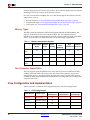
Core Configuration and Implementation . . . . . . . . . . . . . . . . . . . . . . . . . . . . . . . . . . . . 18
Independent Clocks: Block RAM and Distributed RAM . . . . . . . . . . . . . . . . . . . . . . . .
Independent Clocks: Virtex-5 and Virtex-4 Built-in FIFO . . . . . . . . . . . . . . . . . . . . . . .
Common Clock: Block RAM, Distributed RAM, Shift Register . . . . . . . . . . . . . . . . . .
Common Clock: Virtex-5 and Virtex-4 Built-in FIFO . . . . . . . . . . . . . . . . . . . . . . . . . . .
19
19
19
20
FIFO Generator Features . . . . . . . . . . . . . . . . . . . . . . . . . . . . . . . . . . . . . . . . . . . . . . . . . . . . 20
FIFO Interfaces. . . . . . . . . . . . . . . . . . . . . . . . . . . . . . . . . . . . . . . . . . . . . . . . . . . . . . . . . . . . . . 21
Interface Signals: FIFOs With Independent Clocks . . . . . . . . . . . . . . . . . . . . . . . . . . . . 21
Interface Signals: FIFOs with Common Clock . . . . . . . . . . . . . . . . . . . . . . . . . . . . . . . . . 26
Chapter 3: Generating the Core
CORE Generator Graphical User Interface . . . . . . . . . . . . . . . . . . . . . . . . . . . . . . . . . . . 29
FIFO Implementation . . . . . . . . . . . . . . . . . . . . . . . . . . . . . . . . . . . . . . . . . . . . . . . . . . . . . . . 30
Component Name . . . . . . . . . . . . . . . . . . . . . . . . . . . . . . . . . . . . . . . . . . . . . . . . . . . . . . . .
FIFO Implementation . . . . . . . . . . . . . . . . . . . . . . . . . . . . . . . . . . . . . . . . . . . . . . . . . . . . .
Common Clock (CLK), Block RAM . . . . . . . . . . . . . . . . . . . . . . . . . . . . . . . . . . . . . . . .
Common Clock (CLK), Distributed RAM . . . . . . . . . . . . . . . . . . . . . . . . . . . . . . . . . . . .
Common Clock (CLK), Shift Register . . . . . . . . . . . . . . . . . . . . . . . . . . . . . . . . . . . . . . .
Common Clock (CLK), Built-in FIFO . . . . . . . . . . . . . . . . . . . . . . . . . . . . . . . . . . . . . . .
Independent Clocks (RD_CLK, WR_CLK), Block RAM . . . . . . . . . . . . . . . . . . . . . . . . .
FIFO Generator v3.3 User Guide
UG175 April 2, 2007
www.xilinx.com
30
30
30
30
30
31
31
R
Independent Clocks (RD_CLK, WR_CLK), Distributed RAM . . . . . . . . . . . . . . . . . . . . 31
Independent Clocks (RD_CLK, WR_CLK), Built-in FIFO . . . . . . . . . . . . . . . . . . . . . . . . 31
Performance Options and Data Port Parameters . . . . . . . . . . . . . . . . . . . . . . . . . . . . . . 31
Performance Options . . . . . . . . . . . . . . . . . . . . . . . . . . . . . . . . . . . . . . . . . . . . . . . . . . . . . .
Standard FIFO. . . . . . . . . . . . . . . . . . . . . . . . . . . . . . . . . . . . . . . . . . . . . . . . . . . . . . . . .
First-word Fall-through FIFO . . . . . . . . . . . . . . . . . . . . . . . . . . . . . . . . . . . . . . . . . . . . .
Data Port Parameters . . . . . . . . . . . . . . . . . . . . . . . . . . . . . . . . . . . . . . . . . . . . . . . . . . . . . .
Input Data Width . . . . . . . . . . . . . . . . . . . . . . . . . . . . . . . . . . . . . . . . . . . . . . . . . . . . . .
Input Depth . . . . . . . . . . . . . . . . . . . . . . . . . . . . . . . . . . . . . . . . . . . . . . . . . . . . . . . . . .
Output Data Width . . . . . . . . . . . . . . . . . . . . . . . . . . . . . . . . . . . . . . . . . . . . . . . . . . . . .
Output Depth . . . . . . . . . . . . . . . . . . . . . . . . . . . . . . . . . . . . . . . . . . . . . . . . . . . . . . . . .
Built-in FIFO Options . . . . . . . . . . . . . . . . . . . . . . . . . . . . . . . . . . . . . . . . . . . . . . . . . . .
32
32
32
32
32
32
32
32
32
Optional Flags, Handshaking, and Initialization . . . . . . . . . . . . . . . . . . . . . . . . . . . . . 33
Optional Flags. . . . . . . . . . . . . . . . . . . . . . . . . . . . . . . . . . . . . . . . . . . . . . . . . . . . . . . . . . . .
Almost Full Flag . . . . . . . . . . . . . . . . . . . . . . . . . . . . . . . . . . . . . . . . . . . . . . . . . . . . . . .
Almost Empty Flag . . . . . . . . . . . . . . . . . . . . . . . . . . . . . . . . . . . . . . . . . . . . . . . . . . . . .
Write Port Handshaking . . . . . . . . . . . . . . . . . . . . . . . . . . . . . . . . . . . . . . . . . . . . . . . . . . .
Write Acknowledge . . . . . . . . . . . . . . . . . . . . . . . . . . . . . . . . . . . . . . . . . . . . . . . . . . . .
Overflow (Write Error) . . . . . . . . . . . . . . . . . . . . . . . . . . . . . . . . . . . . . . . . . . . . . . . . . .
Read Port Handshaking . . . . . . . . . . . . . . . . . . . . . . . . . . . . . . . . . . . . . . . . . . . . . . . . . . .
Valid (Read Acknowledge) . . . . . . . . . . . . . . . . . . . . . . . . . . . . . . . . . . . . . . . . . . . . . . .
Underflow (Read Error) . . . . . . . . . . . . . . . . . . . . . . . . . . . . . . . . . . . . . . . . . . . . . . . . .
Initialization . . . . . . . . . . . . . . . . . . . . . . . . . . . . . . . . . . . . . . . . . . . . . . . . . . . . . . . . . . . . .
Reset Pin . . . . . . . . . . . . . . . . . . . . . . . . . . . . . . . . . . . . . . . . . . . . . . . . . . . . . . . . . . . . .
33
33
33
33
33
34
34
34
34
34
34
Programmable Flags. . . . . . . . . . . . . . . . . . . . . . . . . . . . . . . . . . . . . . . . . . . . . . . . . . . . . . . . . 35
Programmable Flags . . . . . . . . . . . . . . . . . . . . . . . . . . . . . . . . . . . . . . . . . . . . . . . . . . . . . . 35
Programmable Full Type . . . . . . . . . . . . . . . . . . . . . . . . . . . . . . . . . . . . . . . . . . . . . . . . 35
Programmable Empty Type . . . . . . . . . . . . . . . . . . . . . . . . . . . . . . . . . . . . . . . . . . . . . . 35
Data Count and Reset . . . . . . . . . . . . . . . . . . . . . . . . . . . . . . . . . . . . . . . . . . . . . . . . . . . . . . . 36
Data Count and Reset Options . . . . . . . . . . . . . . . . . . . . . . . . . . . . . . . . . . . . . . . . . . . . . . 36
Data Count . . . . . . . . . . . . . . . . . . . . . . . . . . . . . . . . . . . . . . . . . . . . . . . . . . . . . . . . . . . 36
Resets . . . . . . . . . . . . . . . . . . . . . . . . . . . . . . . . . . . . . . . . . . . . . . . . . . . . . . . . . . . . . . . 37
Summary . . . . . . . . . . . . . . . . . . . . . . . . . . . . . . . . . . . . . . . . . . . . . . . . . . . . . . . . . . . . . . . . . . . 37
Chapter 4: Designing with the Core
General Design Guidelines . . . . . . . . . . . . . . . . . . . . . . . . . . . . . . . . . . . . . . . . . . . . . . . . . 39
Know the Degree of Difficulty . . . . . . . . . . . . . . . . . . . . . . . . . . . . . . . . . . . . . . . . . . . . . . 39
Understand Signal Pipelining and Synchronization . . . . . . . . . . . . . . . . . . . . . . . . . . . 39
Synchronization Considerations . . . . . . . . . . . . . . . . . . . . . . . . . . . . . . . . . . . . . . . . . . . 39
Initializing the FIFO Generator . . . . . . . . . . . . . . . . . . . . . . . . . . . . . . . . . . . . . . . . . . . . . . 40
FIFO Implementations . . . . . . . . . . . . . . . . . . . . . . . . . . . . . . . . . . . . . . . . . . . . . . . . . . . . . . 41
Independent Clocks: Block RAM and Distributed RAM . . . . . . . . . . . . . . . . . . . . . . . .
Independent Clocks: Built-in FIFO . . . . . . . . . . . . . . . . . . . . . . . . . . . . . . . . . . . . . . . . . .
Common Clock: Built-in FIFO . . . . . . . . . . . . . . . . . . . . . . . . . . . . . . . . . . . . . . . . . . . . . .
Common Clock FIFO: Block RAM and Distributed RAM . . . . . . . . . . . . . . . . . . . . . . .
Common Clock FIFO: Shift Registers . . . . . . . . . . . . . . . . . . . . . . . . . . . . . . . . . . . . . . . .
41
42
44
44
44
FIFO Usage and Control . . . . . . . . . . . . . . . . . . . . . . . . . . . . . . . . . . . . . . . . . . . . . . . . . . . . . 45
Write Operation . . . . . . . . . . . . . . . . . . . . . . . . . . . . . . . . . . . . . . . . . . . . . . . . . . . . . . . . . .
ALMOST_FULL and FULL Flags . . . . . . . . . . . . . . . . . . . . . . . . . . . . . . . . . . . . . . . . . .
Example Operation . . . . . . . . . . . . . . . . . . . . . . . . . . . . . . . . . . . . . . . . . . . . . . . . . . . . .
Read Operation . . . . . . . . . . . . . . . . . . . . . . . . . . . . . . . . . . . . . . . . . . . . . . . . . . . . . . . . . .
www.xilinx.com
45
45
46
46
FIFO Generator v3.3 User Guide
UG175 April 2, 2007
R
ALMOST_EMPTY and EMPTY Flags . . . . . . . . . . . . . . . . . . . . . . . . . . . . . . . . . . . . . . . 46
Modes of Read Operation . . . . . . . . . . . . . . . . . . . . . . . . . . . . . . . . . . . . . . . . . . . . . . . . 47
Handshaking Flags . . . . . . . . . . . . . . . . . . . . . . . . . . . . . . . . . . . . . . . . . . . . . . . . . . . . . . .
Write Acknowledge . . . . . . . . . . . . . . . . . . . . . . . . . . . . . . . . . . . . . . . . . . . . . . . . . . . .
Valid . . . . . . . . . . . . . . . . . . . . . . . . . . . . . . . . . . . . . . . . . . . . . . . . . . . . . . . . . . . . . . . .
Example Operation . . . . . . . . . . . . . . . . . . . . . . . . . . . . . . . . . . . . . . . . . . . . . . . . . . . . .
Underflow . . . . . . . . . . . . . . . . . . . . . . . . . . . . . . . . . . . . . . . . . . . . . . . . . . . . . . . . . . . .
Overflow . . . . . . . . . . . . . . . . . . . . . . . . . . . . . . . . . . . . . . . . . . . . . . . . . . . . . . . . . . . . .
Example Operation . . . . . . . . . . . . . . . . . . . . . . . . . . . . . . . . . . . . . . . . . . . . . . . . . . . . .
Programmable Flags . . . . . . . . . . . . . . . . . . . . . . . . . . . . . . . . . . . . . . . . . . . . . . . . . . . . . .
Programmable Full . . . . . . . . . . . . . . . . . . . . . . . . . . . . . . . . . . . . . . . . . . . . . . . . . . . . .
Programmable Empty . . . . . . . . . . . . . . . . . . . . . . . . . . . . . . . . . . . . . . . . . . . . . . . . . . .
Data Counts . . . . . . . . . . . . . . . . . . . . . . . . . . . . . . . . . . . . . . . . . . . . . . . . . . . . . . . . . . . . .
Read Data Count . . . . . . . . . . . . . . . . . . . . . . . . . . . . . . . . . . . . . . . . . . . . . . . . . . . . . . .
Write Data Count . . . . . . . . . . . . . . . . . . . . . . . . . . . . . . . . . . . . . . . . . . . . . . . . . . . . . .
First-Word Fall-Through Data Count . . . . . . . . . . . . . . . . . . . . . . . . . . . . . . . . . . . . . . .
Example Operation . . . . . . . . . . . . . . . . . . . . . . . . . . . . . . . . . . . . . . . . . . . . . . . . . . . . .
Non-symmetric Aspect Ratios . . . . . . . . . . . . . . . . . . . . . . . . . . . . . . . . . . . . . . . . . . . . . .
Built-in Error Correction Checking . . . . . . . . . . . . . . . . . . . . . . . . . . . . . . . . . . . . . . . . . .
Reset Behavior . . . . . . . . . . . . . . . . . . . . . . . . . . . . . . . . . . . . . . . . . . . . . . . . . . . . . . . . . . .
Asynchronous Reset . . . . . . . . . . . . . . . . . . . . . . . . . . . . . . . . . . . . . . . . . . . . . . . . . . . .
Synchronous Reset . . . . . . . . . . . . . . . . . . . . . . . . . . . . . . . . . . . . . . . . . . . . . . . . . . . . .
49
49
49
50
51
51
51
52
52
54
55
56
56
57
57
58
60
61
61
63
Chapter 5: Special Design Considerations
Resetting the FIFO . . . . . . . . . . . . . . . . . . . . . . . . . . . . . . . . . . . . . . . . . . . . . . . . . . . . . . . . . .
Continuous Clocks . . . . . . . . . . . . . . . . . . . . . . . . . . . . . . . . . . . . . . . . . . . . . . . . . . . . . . . . . .
Pessimistic Full and Empty . . . . . . . . . . . . . . . . . . . . . . . . . . . . . . . . . . . . . . . . . . . . . . . . . .
Programmable Full and Empty . . . . . . . . . . . . . . . . . . . . . . . . . . . . . . . . . . . . . . . . . . . . . .
Write Data Count and Read Data Count . . . . . . . . . . . . . . . . . . . . . . . . . . . . . . . . . . . . .
Setup and Hold Time Violations . . . . . . . . . . . . . . . . . . . . . . . . . . . . . . . . . . . . . . . . . . . .
65
65
65
66
66
66
Chapter 6: Simulating Your Design
Simulation Models . . . . . . . . . . . . . . . . . . . . . . . . . . . . . . . . . . . . . . . . . . . . . . . . . . . . . . . . . . 67
Appendix A: Performance Information
Resource Utilization and Performance . . . . . . . . . . . . . . . . . . . . . . . . . . . . . . . . . . . . . . . 69
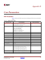
Appendix B: Core Parameters
FIFO Parameters . . . . . . . . . . . . . . . . . . . . . . . . . . . . . . . . . . . . . . . . . . . . . . . . . . . . . . . . . . . . 73
FIFO Generator v3.3 User Guide
UG175 April 2, 2007
www.xilinx.com
R
www.xilinx.com
FIFO Generator v3.3 User Guide
UG175 April 2, 2007
Schedule of Figures
Chapter 2: Core Overview
Figure 2-1: FIFO with Independent Clocks: Interface Signals . . . . . . . . . . . . . . . . . . . . . . 21
Chapter 3: Generating the Core
Figure 3-1:
Figure 3-2:
Figure 3-3:
Figure 3-4:
Figure 3-5:
Figure 3-6:
Main FIFO Generator Screen . . . . . . . . . . . . . . . . . . . . . . . . . . . . . . . . . . . . . . . . .
Performance Options and Data Port Parameters Screen . . . . . . . . . . . . . . . . .
Optional Flags, Handshaking, and Initialization Options Screen. . . . . . . . .
Programmable Flags Screen . . . . . . . . . . . . . . . . . . . . . . . . . . . . . . . . . . . . . . . . . .
Data Count and Reset Screen. . . . . . . . . . . . . . . . . . . . . . . . . . . . . . . . . . . . . . . . .
Summary Screen. . . . . . . . . . . . . . . . . . . . . . . . . . . . . . . . . . . . . . . . . . . . . . . . . . . .
30
31
33
35
36
37
Chapter 4: Designing with the Core
Figure 4-1: FIFO with Independent Clocks: Write and Read Clock Domains . . . . . . . . .
Figure 4-2: Functional Implementation of a FIFO with Independent Clock Domains .
Figure 4-3: Functional Implementation of Built-in FIFO . . . . . . . . . . . . . . . . . . . . . . . . . . .
Figure 4-4: Functional Implementation of a Common Clock FIFO using
Block RAM or Distributed RAM . . . . . . . . . . . . . . . . . . . . . . . . . . . . . . . . . . . . . . . . . . . . .
Figure 4-5: Functional Implementation of a Common Clock FIFO using
Shift Registers . . . . . . . . . . . . . . . . . . . . . . . . . . . . . . . . . . . . . . . . . . . . . . . . . . . . . . . . . . . . .
Figure 4-6: Write Operation for a FIFO with Independent Clocks. . . . . . . . . . . . . . . . . . .
Figure 4-7: Standard Read Operation for a FIFO with Independent Clocks . . . . . . . . . .
Figure 4-8: FWFT Read Operation for a FIFO with Independent Clocks . . . . . . . . . . . . .
Figure 4-9: Write and Read Operation for a FIFO with Common Clocks . . . . . . . . . . . . .
Figure 4-10: Handshaking Signals for a FIFO with Independent Clocks . . . . . . . . . . . . .
Figure 4-11: Handshaking Signals for a FIFO with Common Clocks . . . . . . . . . . . . . . . .
Figure 4-12: Programmable Full Single Threshold: Threshold Set to 7. . . . . . . . . . . . . . .
Figure 4-13: Programmable Full with Assert and Negate Thresholds:
Assert Set to 10 and Negate Set to 7 . . . . . . . . . . . . . . . . . . . . . . . . . . . . . . . . . . . . . . . . . . .
Figure 4-14: Programmable Empty with Single Threshold: Threshold Set to 4 . . . . . . .
Figure 4-15: Programmable Empty with Assert and Negate Thresholds:
Assert Set to 7 and Negate Set to 10 . . . . . . . . . . . . . . . . . . . . . . . . . . . . . . . . . . . . . . . . . . .
Figure 4-16: Write and Read Data Counts for FIFO with Independent Clocks . . . . . . . .
Figure 4-17: 1:4 Aspect Ratio: Data Ordering . . . . . . . . . . . . . . . . . . . . . . . . . . . . . . . . . . . . .
Figure 4-18: 1:4 Aspect Ratio: Status Flag Behavior. . . . . . . . . . . . . . . . . . . . . . . . . . . . . . . .
Figure 4-19: 4:1 Aspect Ratio: Data Ordering . . . . . . . . . . . . . . . . . . . . . . . . . . . . . . . . . . . . .
Figure 4-20: 4:1 Aspect Ratio: Status Flag Behavior . . . . . . . . . . . . . . . . . . . . . . . . . . . . . . .
Figure 4-21: SBITERR and DBITERR Outputs in the FIFO Generator Core . . . . . . . . . .
Figure 4-22: Synchronous Reset: FIFO with Independent Clock . . . . . . . . . . . . . . . . . . . .
Figure 4-23: Asynchronous Reset: FIFO with Common Clock . . . . . . . . . . . . . . . . . . . . . .
Figure 4-24: Synchronous Reset: FIFO with a Common Clock . . . . . . . . . . . . . . . . . . . . . .
FIFO Generator v3.3 User Guide
UG175 April 2, 2007
www.xilinx.com
40
41
43
44
45
46
48
48
49
50
51
53
53
54
55
57
58
59
59
60
61
62
62
63
7
R
8
www.xilinx.com
FIFO Generator v3.3 User Guide
UG175 April 2, 2007
Schedule of Tables
Chapter 2: Core Overview
Table 2-1: Memory Configuration Benefits . . . . . . . . . . . . . . . . . . . . . . . . . . . . . . . . . . . . . . . 18
Table 2-2: FIFO Configurations . . . . . . . . . . . . . . . . . . . . . . . . . . . . . . . . . . . . . . . . . . . . . . . . . 18
Table 2-3: FIFO Configurations Summary. . . . . . . . . . . . . . . . . . . . . . . . . . . . . . . . . . . . . . . . 20
Table 2-4: Reset Signal for FIFOs with Independent Clocks . . . . . . . . . . . . . . . . . . . . . . . . 21
Table 2-5: Write Interface Signals for FIFOs with Independent Clocks . . . . . . . . . . . . . . 22
Table 2-6: Read Interface Signals for FIFOs with Independent Clocks. . . . . . . . . . . . . . . 23
Table 2-7: Interface Signals for FIFOs with a Common Clock . . . . . . . . . . . . . . . . . . . . . . 26
Chapter 4: Designing with the Core
Table 4-1: Interface Signals and Corresponding Clock Domains . . . . . . . . . . . . . . . . . . . . 42
Table 4-2: Interface Signals and Corresponding Clock Domains . . . . . . . . . . . . . . . . . . . . 43
Table 4-3: Implementation-Specific Support for First-Word Fall-Through . . . . . . . . . . . 47
Table 4-4: Implementation-specific Support for Data Counts. . . . . . . . . . . . . . . . . . . . . . . 56
Table 4-5: Implementation-specific Support for Non-symmetric Aspect Ratios . . . . . . . 58
Table 4-6: FIFO Reset Values . . . . . . . . . . . . . . . . . . . . . . . . . . . . . . . . . . . . . . . . . . . . . . . . . . . 62
Table 4-7: FIFO Reset and Power-up Values . . . . . . . . . . . . . . . . . . . . . . . . . . . . . . . . . . . . . . 64
Appendix A: Performance Information
Table A-1: Benchmarks: FIFO Configured without Optional Features . . . . . . . . . . . . . . . 69
Table A-2: Benchmarks: FIFO Configured with Multiple Programmable Thresholds . 70
Table A-3: Benchmarks: FIFO Configured with Virtex-5 FIFO36 Resources. . . . . . . . . . 71
Table A-4: Benchmarks: FIFO Configured with Virtex-4 FIFO16 Patch . . . . . . . . . . . . . . 72
Appendix B: Core Parameters
Table B-1: FIFO Parameter Table . . . . . . . . . . . . . . . . . . . . . . . . . . . . . . . . . . . . . . . . . . . . . . . . 73
FIFO Generator v3.3 User Guide
UG175 April 2, 2007
www.xilinx.com
R
www.xilinx.com
FIFO Generator v3.3 User Guide
UG175 April 2, 2007
R
Preface
About This Guide
The LogicCORE™ FIFO Generator User Guide v3.3 describes the function and operation of
the FIFO Generator, as well as information about designing, customizing, and
implementing the core.
Guide Contents
The following chapters are included:
•
“Preface, About this Guide” describes how the user guide is organized, the
conventions used in the guide, and information about additional resources.
•
Chapter 1, “Introduction,” describes the core and related information, including
recommended design experience, additional resources, technical support, and
submitting feedback to Xilinx.
•
Chapter 2, “Core Overview,” describes the core configuration options and their
interfaces.
•
Chapter 3, “Generating the Core,” describes how to generate the core using the Xilinx
CORE Generator Graphical User Interface (GUI).
•
Chapter 4, “Designing with the Core,” discusses how to use the core in a user
application.
•
Chapter 5, “Special Design Considerations,” discusses specific design features that
must be considered when designing with the core.
•
Chapter 6, “Simulating Your Design,” provides instructions for simulating the design
with either behavioral or structural simulation models.
•
Appendix A, “Performance Information,” provides a summary of the core’s
performance data.
•
Appendix B, “Core Parameters,” provides a comprehensive list of the parameters set
by the CORE Generator GUI for the FIFO Generator.
FIFO Generator v3.3 User Guide
UG175 April 2, 2007
www.xilinx.com
11
R
Chapter : About This Guide
Additional Resources
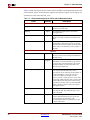
For additional information, go to www.xilinx.com/support. The following table lists some
of the resources you can access from this website or by using the provided URLs.
Resource
Tutorials
Description/URL
Tutorials covering Xilinx design flows, from design entry to
verification and debugging
www.xilinx.com/support/techsup/tutorials/index.htm
Answer Browser
Database of Xilinx solution records
www.xilinx.com/xlnx/xil_ans_browser.jsp
Data Sheets
Device-specific information on Xilinx device characteristics,
including readback, boundary scan, configuration, length count,
and debugging
www.xilinx.com/xlnx/xweb/xil_publications_index.jsp
Problem Solvers
Interactive tools that allow you to troubleshoot your design issues
www.xilinx.com/support/troubleshoot/psolvers.htm
Tech Tips
Latest news, design tips, and patch information for the Xilinx
design environment
www.xilinx.com/xlnx/xil_tt_home.jsp
Conventions
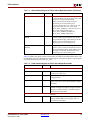
This document uses the following conventions. An example illustrates each convention.
Typographical
The following typographical conventions are used in this document:
Convention
Example
Courier font
Messages, prompts, and
program files that the system
displays and signal names
speed grade: - 100
Courier bold
Literal commands you enter in
a syntactical statement
ngdbuild design_name
Variables in a syntax
statement for which you must
supply values
See the Development System
Reference Guide for more
information.
References to other manuals
See the User Guide for details.
Emphasis in text
If a wire is drawn so that it
overlaps the pin of a symbol,
the two nets are not connected.
Items that are not supported
or reserved
This feature is not supported
Italic font
Dark Shading
12
Meaning or Use
www.xilinx.com
FIFO Generator v3.3 User Guide
UG175 April 2, 2007
R
Conventions
Convention
Meaning or Use
Example
An optional entry or
parameter. However, in bus
specifications, such as
bus[7:0], they are required.
ngdbuild [option_name]
design_name
A list of items from which you
must choose one or more
lowpwr ={on|off}
Separates items in a list of
choices
lowpwr ={on|off}
Vertical ellipsis
.
.
.
Repetitive material that has
been omitted
IOB #1: Name = QOUT’
IOB #2: Name = CLKIN’
.
.
.
Horizontal ellipsis . . .
Omitted repetitive material
allow block block_name
loc1 loc2 ... locn;
The prefix ‘0x’ or the suffix ‘h’
indicate hexadecimal notation
A read of address
0x00112975 returned
45524943h.
An ‘_n’ means the signal is
active low
usr_teof_n is active low.
Square brackets
Braces
[ ]
{ }
Vertical bar
|
Notations
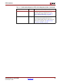
Online Document
The following linking conventions are used in this document:
Convention
Meaning or Use
Blue text
Cross-reference link to a
location in the current
document
Blue, underlined text
Hyperlink to a website (URL)
FIFO Generator v3.3 User Guide
UG175 April 2, 2007
www.xilinx.com
Example
See the section “Additional
Resources” for details.
See “Title Formats” in Chapter
1 for details.
Go to http://www.xilinx.com
for the latest speed files.
13
R
14
Chapter : About This Guide
www.xilinx.com
FIFO Generator v3.3 User Guide
UG175 April 2, 2007
R
Chapter 1
Introduction
The FIFO Generator core, a fully verified first-in first-out memory queue for use in any
application requiring in-order storage and retrieval, enables high-performance and areaoptimized designs. This core can be customized using the Xilinx CORE Generator™
system as a complete solution with control logic already implemented, including
management of the read and write pointers and the generation of status flags.
This chapter introduces the FIFO Generator and provides related information, including
recommended design experience, additional resources, technical support, and submitting
feedback to Xilinx.
About the Core
The FIFO Generator is a Xilinx CORE Generator IP core, included in the latest IP Update on
the Xilinx IP Center. The core is free of charge and no license is required. For detailed
information about the core, see
www.xilinx.com/xlnx/xebiz/designResources/ip_product_details.jsp?key=FIFO_Generator.
Recommended Design Experience
The FIFO Generator is a fully verified solution, and can be used by all levels of design
engineers.
Important: When implementing a FIFO with independent write and read clocks, special
care must be taken to ensure the FIFO Generator is correctly used. “Synchronization
Considerations,” page 39 provides important information to help ensure correct design
configuration.
Similarly, asynchronous designs should also be aware that the behavioral models are not
cycle-accurate across clock domains. See Chapter 6, “Simulating Your Design,” for details.
Technical Support
For technical support, visit www.support.xilinx.com/. Questions are routed to a team of
engineers with FIFO Generator expertise.
Xilinx will provide technical support for use of this product as described in the LogiCORE
FIFO Generator User Guide. Xilinx cannot guarantee timing, functionality, or support of this
product for designs that do not follow these guidelines.
FIFO Generator v3.3 User Guide
UG175 April 2, 2007
www.xilinx.com
15
R
Chapter 1: Introduction
Feedback
Xilinx welcomes comments and suggestions about the FIFO Generator and the
documentation supplied with the core.
FIFO Generator
For comments or suggestions about the FIFO Generator, please submit a WebCase from
www.support.xilinx.com/. Be sure to include the following information:
•
Product name
•
Core version number
•
Explanation of your comments
Document
For comments or suggestions about this document, please submit a WebCase from
www.support.xilinx.com/. Be sure to include the following information:
16
•
Document title
•
Document number
•
Page number(s) to which your comments refer
•
Explanation of your comments
www.xilinx.com
FIFO Generator v3.3 User Guide
UG175 April 2, 2007
R
Chapter 2
Core Overview
This chapter provides an overview of the FIFO Generator configuration options and
interfaces.
System Overview
Clock Implementation Operation
The FIFO Generator enables FIFOs to be configured with either independent or common
clock domains for write and read operations. The independent clock configuration of the
FIFO Generator enables the user to implement unique clock domains on the write and read
ports. The FIFO Generator handles the synchronization between clock domains, placing no
requirements on phase and frequency relationships between clocks. A common clock
domain implementation optimizes the core for data buffering within a single clock
domain.
Built-in FIFO Support in Virtex-5
The FIFO Generator supports the VirtexTM-5 built-in FIFO modules, enabling large FIFOs
to be created by cascading the built-in FIFOs in both width and depth. The core expands
the capabilities of the built-in FIFOs by utilizing the FPGA fabric to create optional status
flags not implemented in the built-in FIFO macro. The built-in Error Correction Checking
(ECC) feature in the built-in FIFO macro is also available to the user.
Built-in FIFO Support in Virtex-4
The FIFO Generator supports a single instantiation of the Virtex-4 built-in FIFO module.
The core also implements a FIFO flag patch (“Solution 1: Synchronous/Asynchronous
Clock Work-Arounds,” defined in the Virtex-4 User Guide), based on estimated clock
frequencies. This patch is implemented in fabric. See Appendix A, “Performance
Information” for resource utilization estimates.
First-Word Fall-Through
The first-word fall-through (FWFT) feature provides the ability to look ahead to the next
word available from the FIFO without having to issue a read operation. The FIFO
accomplishes this by using output registers which are automatically loaded with data,
when data appears in the FIFO. This causes the first word written to the FIFO to
automatically appear on the data out bus (DOUT). Subsequent user read operations cause
the output data to update with the next word, as long as data is available in the FIFO. The
use of registers on the FIFO DOUT bus improves clock-to-output timing, and the FWFT
FIFO Generator v3.3 User Guide
UG175 April 2, 2007
www.xilinx.com
17
R
Chapter 2: Core Overview
functionality provides low-latency access to data. This is ideal for applications that require
throttling, based on the contents of the data that are read.
See Table 2-2 for FWFT availability. The use of this feature impacts the behavior of many
other features, such as:
•
Read operations (see “First-Word Fall-Through FIFO Read Operation,” page 48)
•
Programmable empty (see “Programmable Empty for First-Word Fall-Through,” page 55)
•
Data counts (see “First-Word Fall-Through Data Count,” page 57)
Memory Types
The FIFO Generator implements FIFOs built from block RAM, distributed RAM, shift
registers, or the Virtex-4 and Virtex-5 built-in FIFOs. The core combines memory
primitives in an optimal configuration based on the selected width and depth of the FIFO.
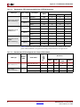
Table 2-1 provides best-use recommendations for specific design requirements.
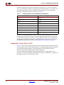
Table 2-1:
Memory Configuration Benefits
Independent Common
Small
Clocks
Clock
Buffering
MediumLarge
Buffering
High
Minimal
Performance Resources
Built-in
FIFO
✔
✔
✔
✔
✔
Block RAM
✔
✔
✔
✔
✔
Shift
Register
✔
Distributed
RAM
✔
✔
✔
✔
✔
✔
Non-Symmetric Aspect Ratio
The core supports generating FIFOs whose write and read ports have different widths,
enabling automatic width conversion of the data width. Non-symmetric aspect ratios
ranging from 1:8 to 8:1 are supported for the write and read port widths. This feature is
available for FIFOs implemented with block RAM that are configured to have independent
write and read clocks.
Core Configuration and Implementation
Table 2-2 provides a summary of the supported memory and clock configurations.
Table 2-2:
FIFO Configurations
Clock Domain
18
Memory Type
Supported
Configuration
Common
Block RAM
✔
Common
Distributed RAM
✔
Common
Shift Register
✔
Common
Built-in FIFO 1
✔
www.xilinx.com
Non-symmetric
Aspect Ratios
First-Word
Fall-Through
✔2
FIFO Generator v3.3 User Guide
UG175 April 2, 2007
R
Core Configuration and Implementation
Table 2-2:
FIFO Configurations (Continued)
Clock Domain
Memory Type
Supported
Configuration
Non-symmetric
Aspect Ratios
First-Word
Fall-Through
✔
✔
Independent
Block RAM
✔
Independent
Distributed RAM
✔
✔
Independent
Built-in FIFO1
✔
✔2
1. The built-in FIFO primitive is only available in Virtex-5 and Virtex-4 architectures.
2. Only valid in Virtex-5 built-in FIFO primitives.
Independent Clocks: Block RAM and Distributed RAM
This implementation category allows the user to select block RAM or distributed RAM and
supports independent clock domains for write and read data accesses. Operations in the
read domain are synchronous to the read clock and operations in the write domain are
synchronous to the write clock.
The feature set supported for this type of FIFO includes non-symmetric aspect ratios
(different write and read port widths), status flags (full, almost full, empty, and almost
empty), as well as programmable full and empty flags generated with user-defined
thresholds. Optional read data count and write data count indicators provide the number
of words in the FIFO relative to their respective clock domains. In addition, optional
handshaking and error flags are available (write acknowledge, overflow, valid, and
underflow).
Independent Clocks: Virtex-5 and Virtex-4 Built-in FIFO
This implementation category allows you to select the built-in FIFO that is available in the
Virtex-5 and Virtex-4 architectures. Operations in the read domain are synchronous to the
read clock and operations in the write domain are synchronous to the write clock.
The feature set supported for this configuration includes status flags (full and empty) and
programmable full and empty flags generated with user-defined thresholds. In addition,
optional handshaking and error flags are available (write acknowledge, overflow, valid,
and underflow). The Virtex-5 built-in FIFO configuration also supports the built-in ECC
feature.
Common Clock: Block RAM, Distributed RAM, Shift Register
This implementation category allows the user to select block RAM, distributed RAM, or
shift register and supports a common clock for write and read data accesses.
The feature set supported for this configuration includes status flags (full, almost full,
empty, and almost empty) and programmable empty and full flags generated with userdefined thresholds. In addition, optional handshaking and error flags are supported (write
acknowledge, overflow, valid, and underflow), and an optional data count provides the
number of words in the FIFO. For block RAM and distributed RAM implementations,
optional synchronous or asynchronous reset pin is available.
FIFO Generator v3.3 User Guide
UG175 April 2, 2007
www.xilinx.com
19
R
Chapter 2: Core Overview
Common Clock: Virtex-5 and Virtex-4 Built-in FIFO
This implementation category allows you to select the built-in FIFO that is available in the
Virtex-5 and Virtex-4 architectures, and supports a common clock for write and read data
accesses.
The feature set supported for this configuration includes status flags (full and empty) and
optional programmable full and empty flags with user-defined thresholds. In addition,
optional handshaking and error flags are available (write acknowledge, overflow, valid,
and underflow). The built-in FIFO configuration also supports the built-in ECC feature.
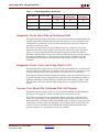
FIFO Generator Features
Table 2-3 summarizes the FIFO Generator features supported for each clock configuration
and memory type.
Table 2-3:
FIFO Configurations Summary
Independent Clocks
FIFO Feature
Block RAM
Common Clock
Distribute
RAM
Built-in
FIFO
Block RAM
Distributed
RAM, Shift
Register
Built-in
FIFO
✔
✔
✔
✔
Non-symmetric
Aspect Ratios1
✔
Symmetric
Aspect Ratios
✔
✔
Almost Full
✔
✔
✔
✔
Almost Empty
✔
✔
✔
✔
Handshaking
✔
✔
✔
✔
Data Count
✔
✔
✔
✔
Programmable
Empty/Full
Thresholds
✔
✔
✔
✔
✔
First-Word FallThrough
✔
✔
✔2
✔
Synchronous
Reset
Asynchronous
Reset
✔4
✔4
DOUT Reset
Value
✔5
✔
✔
✔6
ECC
✔
✔
✔2
✔
✔3
✔4
✔4
✔5
✔
✔
✔6
1. For applications with a single clock that require non-symmetric ports, use the independent clock configuration and
connect the write and read clocks to the same source. A dedicated solution for common clocks will be available in a
future release. Contact your Xilinx representative for more details.
2. FWFT is only supported for the Virtex-5 built-in FIFOs.
3. Synchronous reset is available for common clock configurations using distributed and block RAM only.
4. Asynchronous reset is optional for all FIFOs built using distributed and block RAM.
5. All architectures except for Virtex, Virtex-E, Spartan-II, and Spartan-IIE.
6. ECC is only supported for the Virtex-5 built-in FIFOs.
20
www.xilinx.com
FIFO Generator v3.3 User Guide
UG175 April 2, 2007
R
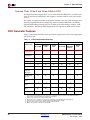
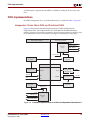
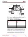
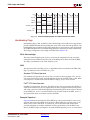
FIFO Interfaces
FIFO Interfaces
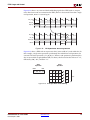
The following two sections provide definitions for the FIFO interface signals. Figure 2-1
illustrates these signals (both the standard and optional ports) for a FIFO core that supports independent write and read clocks.
DIN[N:0]
DOUT[M:0]
WR_EN
RD_EN
WR_CLK
RD_CLK
FULL
EMPTY
ALMOST_FULL
PROG_FULL
ALMOST_EMPTY
Write Clock
Domain
Read Clock
Domain
PROG_EMPTY
WR_ACK
VALID
OVERFLOW
UNDERFLOW
SBITERR
PROG_FULL_THRESH_ASSERT
DBITERR
PROG_FULL_THRESH_NEGATE
PROG_EMPTY_THRESH_ASSERT
PROG_FULL_THRESH
PROG_EMPTY_THRESH_NEGATE
PROG_EMPTY_THRESH
RST
Note: Optional ports represented in italics
Figure 2-1:
FIFO with Independent Clocks: Interface Signals
Interface Signals: FIFOs With Independent Clocks
The RST signal, as defined in Table 2-4, causes a reset of the entire core logic (both write
and read clock domains). It is an asynchronous input which is synchronized internally in
the core before being used. The initial hardware reset should be generated by the user.
When the core is configured to have independent clocks, the reset signal should be High
for at least three read clock and write clock cycles to ensure all internal states are reset to
the correct values.
Table 2-4:
Reset Signal for FIFOs with Independent Clocks
Name
RST
FIFO Generator v3.3 User Guide
UG175 April 2, 2007
Direction
Input
www.xilinx.com
Description
Reset: An asynchronous reset signal that
initializes all internal pointers and output
registers.
21
R
Chapter 2: Core Overview
Table 2-5 defines the signals for the write interface for FIFOs with independent clocks. The
write interface signals are divided into required and optional signals and all signals are
synchronous to the write clock (WR_CLK).
Table 2-5:
Write Interface Signals for FIFOs with Independent Clocks
Name
Direction
Description
Required
WR_CLK
Input
Write Clock: All signals on the write domain are
synchronous to this clock.
DIN[N:0]
Input
Data Input: The input data bus used when
writing the FIFO.
WR_EN
Input
Write Enable: If the FIFO is not full, asserting this
signal causes data (on DIN) to be written to the
FIFO.
Output
Full Flag: When asserted, this signal indicates
that the FIFO is full. Write requests are ignored
when the FIFO is full, initiating a write when the
FIFO is full is non-destructive to the contents of
the FIFO.
FULL
Optional
22
ALMOST_FULL
Output
Almost Full: When asserted, this signal indicates
that only one more write can be performed before
the FIFO is full.
PROG_FULL
Output
Programmable Full: This signal is asserted when
the number of words in the FIFO is greater than
or equal to the assert threshold. It is deasserted
when the number of words in the FIFO is less
than the negate threshold.
WR_DATA_COUNT [D:0]
Output
Write Data Count: This bus indicates the number
of words stored in the FIFO. The count is
guaranteed to never under-report the number of
words in the FIFO, to ensure the user never
overflows the FIFO. The exception to this
behavior is when a write operation occurs at the
rising edge of WR_CLK, that write operation will
only be reflected on WR_DATA_COUNT at the
next rising clock edge. If D is less than log2(FIFO
depth)-1, the bus is truncated by removing the
least-significant bits.
WR_ACK
Output
Write Acknowledge: This signal indicates that a
write request (WR_EN) during the prior clock
cycle succeeded.
OVERFLOW
Output
Overflow: This signal indicates that a write
request (WR_EN) during the prior clock cycle
was rejected, because the FIFO is full.
Overflowing the FIFO is non-destructive to the
contents of the FIFO.
www.xilinx.com
FIFO Generator v3.3 User Guide
UG175 April 2, 2007
R
FIFO Interfaces
Table 2-5:
Write Interface Signals for FIFOs with Independent Clocks (Continued)
Name
PROG_FULL_THRESH
Direction
Description
Input
Programmable Full Threshold: This signal is used
to input the threshold value for the assertion and
deassertion of the programmable full
(PROG_FULL) flag. The threshold can be
dynamically set in-circuit during reset.
The user can either choose to set the assert and
negate threshold to the same value (using
PROG_FULL_THRESH), or the user can control
these values independently (using
PROG_FULL_THRESH_ASSERT and
PROG_FULL_THRESH_NEGATE).
PROG_FULL_THRESH_
ASSERT
Input
Programmable Full Threshold Assert: This signal
is used to set the upper threshold value for the
programmable full flag, which defines when the
signal is asserted. The threshold can be
dynamically set in-circuit during reset.
PROG_FULL_THRESH_
NEGATE
Input
Programmable Full Threshold Negate: This
signal is used to set the lower threshold value for
the programmable full flag, which defines when
the signal is deasserted. The threshold can be
dynamically set in-circuit during reset.
Table 2-6 defines the signals on the read interface of a FIFO with independent clocks. The
read interface signals are divided into required signals and optional signals, and all signals
are synchronous to the read clock (RD_CLK).
Table 2-6:
Read Interface Signals for FIFOs with Independent Clocks
Name
Direction
Description
Required
RD_CLK
DOUT[M:0]
Input
Output
Read Clock: All signals on the read domain are
synchronous to this clock.
Data Output: The output data bus is driven when
reading the FIFO.
RD_EN
Input
Read Enable: If the FIFO is not empty, asserting this
signal causes data to be read from the FIFO (output
on DOUT).
EMPTY
Output
Empty Flag: When asserted, this signal indicates that
the FIFO is empty. Read requests are ignored when
the FIFO is empty, initiating a read while empty is
non-destructive to the FIFO.
Optional
ALMOST_EMPTY
FIFO Generator v3.3 User Guide
UG175 April 2, 2007
Output
www.xilinx.com
Almost Empty Flag: When asserted, this signal
indicates that the FIFO is almost empty and one
word remains in the FIFO.
23
R
Chapter 2: Core Overview
Table 2-6:
Read Interface Signals for FIFOs with Independent Clocks (Continued)
Name
Direction
Description
PROG_EMPTY
Output
Programmable Empty: This signal is asserted when
the number of words in the FIFO is less than or equal
to the programmable threshold. It is deasserted
when the number of words in the FIFO exceeds the
programmable threshold.
RD_DATA_COUNT [C:0]
Output
Read Data Count: This bus indicates the number of
words available for reading in the FIFO. The count is
guaranteed to never over-report the number of
words available for reading, to ensure that the user
does not underflow the FIFO. The exception to this
behavior is when the read operation occurs at the
rising edge of RD_CLK, that read operation will only
be reflected on RD_DATA_COUNT at the next rising
clock edge. If C is less than log2(FIFO depth)-1, the
bus is truncated by removing the least-significant
bits.
VALID
Output
Valid: This signal indicates that valid data is
available on the output bus (DOUT).
UNDERFLOW
Output
Underflow: Indicates that the read request (RD_EN)
during the previous clock cycle was rejected because
the FIFO is empty. Underflowing the FIFO is not
destructive to the FIFO.
Input
Programmable Empty Threshold: This signal is used
to input the threshold value for the assertion and
deassertion of the programmable empty
(PROG_EMPTY) flag. The threshold can be
dynamically set in-circuit during reset.
PROG_EMPTY_THRESH
The user can either choose to set the assert and
negate threshold to the same value (using
PROG_EMPTY_THRESH), or the user can control
these values independently (using
PROG_EMPTY_THRESH_ASSERT and
PROG_EMPTY_THRESH_NEGATE).
24
PROG_EMPTY_THRESH_
ASSERT
Input
Programmable Empty Threshold Assert: This signal
is used to set the lower threshold value for the
programmable empty flag, which defines when the
signal is asserted. The threshold can be dynamically
set in-circuit during reset.
PROG_EMPTY_THRESH_
NEGATE
Input
Programmable Empty Threshold Negate: This signal
is used to set the upper threshold value for the
programmable empty flag, which defines when the
signal is deasserted. The threshold can be
dynamically set in-circuit during reset.
www.xilinx.com
FIFO Generator v3.3 User Guide
UG175 April 2, 2007
R
FIFO Interfaces
Table 2-6:
Read Interface Signals for FIFOs with Independent Clocks (Continued)
Name
Direction
Description
SBITERR
Output
Single Bit Error: Indicates that the ECC decoder
detected and fixed a single-bit error on a
Virtex-5 built-in FIFO macro. See “Built-in
Error Correction Checking,” page 60.
DBITERR
Output
Double Bit Error: Indicates that the ECC
decoder detected a double-bit error on a
Virtex-5 built-in FIFO macro, and data in the
FIFO core is corrupted. See “Built-in Error
Correction Checking,” page 60.
FIFO Generator v3.3 User Guide
UG175 April 2, 2007
www.xilinx.com
25
R
Chapter 2: Core Overview
Interface Signals: FIFOs with Common Clock
Table 2-7 defines the interface signals of a FIFO with a common write and read clock. The
table is divided into standard and optional interface signals, and all signals (except reset)
are synchronous to the common clock (CLK). Users have the option to select synchronous
or asynchronous reset for the distributed or block RAM FIFO implementation.
Table 2-7:
Interface Signals for FIFOs with a Common Clock
Name
Direction
Description
Required
RST
Input
Reset: An asynchronous reset that initializes
all internal pointers and output registers.
SRST
Input
Synchronous Reset: A synchronous reset that
initializes all internal pointers and output
registers.
CLK
Input
Clock: All signals on the write and read
domains are synchronous to this clock.
DIN[N:0]
Input
Data Input: The input data bus used when
writing the FIFO.
WR_EN
Input
Write Enable: If the FIFO is not full, asserting
this signal causes data (on DIN) to be written
to the FIFO.
FULL
Output
Full Flag: When asserted, this signal indicates
that the FIFO is full. Write requests are
ignored when the FIFO is full, initiating a
write when the FIFO is full is non-destructive
to the contents of the FIFO.
DOUT[M:0]
Output
Data Output: The output data bus driven
when reading the FIFO.
RD_EN
Input
Read Enable: If the FIFO is not empty,
asserting this signal causes data to be read
from the FIFO (output on DOUT).
EMPTY
Output
Empty Flag: When asserted, this signal
indicates that the FIFO is empty. Read
requests are ignored when the FIFO is empty,
initiating a read while empty is nondestructive to the FIFO.
Optional
26
DATA_COUNT [C:0]
Output
Data Count: This bus indicates the number of
words stored in the FIFO. If C is less than
log2(FIFO depth)-1, the bus is truncated by
removing the least-significant bits.
ALMOST_FULL
Output
Almost Full: When asserted, this signal
indicates that only one more write can be
performed before the FIFO is full.
www.xilinx.com
FIFO Generator v3.3 User Guide
UG175 April 2, 2007
R
FIFO Interfaces
Table 2-7:
Interface Signals for FIFOs with a Common Clock (Continued)
Name
Direction
Description
PROG_FULL
Output
Programmable Full: This signal is asserted
when the number of words in the FIFO is
greater than or equal to the assert threshold. It
is deasserted when the number of words in
the FIFO is less than the negate threshold.
WR_ACK
Output
Write Acknowledge: This signal indicates
that a write request (WR_EN) during the
prior clock cycle succeeded.
OVERFLOW
Output
Overflow: This signal indicates that a write
request (WR_EN) during the prior clock cycle
was rejected, because the FIFO is full.
Overflowing the FIFO is non-destructive to
the contents of the FIFO.
Input
Programmable Full Threshold: This signal is
used to set the threshold value for the
assertion and deassertion of the
programmable full flag (PROG_FULL). The
threshold can be dynamically set in-circuit
during reset.
PROG_FULL_THRESH
The user can either choose to set the assert
and negate threshold to the same value (using
PROG_FULL_THRESH), or the user can
control these values independently (using
PROG_FULL_THRESH_ASSERT and
PROG_FULL_THRESH_NEGATE).
PROG_FULL_THRESH_
ASSERT
Input
Programmable Full Threshold Assert: This
signal is used to set the upper threshold value
for the programmable full flag, which defines
when the signal is asserted. The threshold can
be dynamically set in-circuit during reset.
PROG_FULL_THRESH_
NEGATE
Input
Programmable Full Threshold Negate: This
signal is used to set the lower threshold value
for the programmable full flag, which defines
when the signal is deasserted. The threshold
can be dynamically set in-circuit during reset.
ALMOST_EMPTY
Output
Almost Empty Flag: When asserted, this
signal indicates that the FIFO is almost empty
and one word remains in the FIFO.
PROG_EMPTY
Output
Programmable Empty: This signal is asserted
after the number of words in the FIFO is less
than or equal to the programmable threshold.
It is deasserted when the number of words in
the FIFO exceeds the programmable
threshold.
FIFO Generator v3.3 User Guide
UG175 April 2, 2007
www.xilinx.com
27
R
Chapter 2: Core Overview
Table 2-7:
Interface Signals for FIFOs with a Common Clock (Continued)
Name
Direction
Description
VALID
Output
Valid: This signal indicates that valid data is
available on the output bus (DOUT).
UNDERFLOW
Output
Underflow: Indicates that read request
(RD_EN) during the previous clock cycle was
rejected because the FIFO is empty.
Underflowing the FIFO is not destructive to
the FIFO.
Input
Programmable Empty Threshold: This signal
is used to set the threshold value for the
assertion and deassertion of the
programmable empty flag (PROG_EMPTY).
The threshold can be dynamically set incircuit during reset.
PROG_EMPTY_THRESH
The user can either choose to set the assert
and negate threshold to the same value (using
PROG_EMPTY_THRESH), or the user can
control these values independently (using
PROG_EMPTY_THRESH_ASSERT and
PROG_EMPTY_THRESH_NEGATE).
28
PROG_EMPTY_THRESH_
ASSERT
Input
Programmable Empty Threshold Assert: This
signal is used to set the lower threshold value
for the programmable empty flag, which
defines when the signal is asserted. The
threshold can be dynamically set in-circuit
during reset.
PROG_EMPTY_THRESH_
NEGATE
Input
Programmable Empty Threshold Negate:
This signal is used to set the upper threshold
value for the programmable empty flag,
which defines when the signal is deasserted.
The threshold can be dynamically set incircuit during reset.
SBITERR
Output
Single Bit Error: Indicates that the ECC
decoder detected and fixed a single-bit error
on a Virtex-5 built-in FIFO macro. See “Builtin Error Correction Checking,” page 60.
DBITERR
Output
Double Bit Error: Indicates that the ECC
decoder detected a double-bit error on a
Virtex-5 built-in FIFO macro, and data in the
FIFO core is corrupted. See “Built-in Error
Correction Checking,” page 60.
www.xilinx.com
FIFO Generator v3.3 User Guide
UG175 April 2, 2007
R
Chapter 3
Generating the Core
This chapter contains information and instructions for using the Xilinx CORE Generator
system to customize the FIFO Generator.
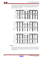
CORE Generator Graphical User Interface
The FIFO Generator GUI includes six configuration screens.
•
FIFO Implementation
•
Performance Options and Data Port Parameters
•
Optional Flags and Handshaking Options
•
Programmable Flags
•
Data Count and Reset
•
Summary
FIFO Generator v3.3 User Guide
UG175 April 2, 2007
www.xilinx.com
29
R
Chapter 3: Generating the Core
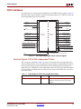
FIFO Implementation
The main FIFO Generator screen is used to define the component name and provides
configuration options for the core.
Figure 3-1:
Main FIFO Generator Screen
Component Name
Base name of the output files generated for this core. The name must begin with a letter
and be composed of the following characters: a to z, 0 to 9, and “_”.
FIFO Implementation
This section of the GUI allows the user to select from a set of available FIFO
implementations and supported features. The key supported features that are only
available for certain implementations are highlighted by checks in the right-margin. The
available options are listed below, with cross-references to additional information.
Common Clock (CLK), Block RAM
For details, see “Common Clock FIFO: Block RAM and Distributed RAM,” page 44.
Common Clock (CLK), Distributed RAM
For details, see “Common Clock FIFO: Block RAM and Distributed RAM,” page 44.
Common Clock (CLK), Shift Register
For details, see “Common Clock FIFO: Shift Registers,” page 44. This implementation is
only available in Virtex-II and newer architectures.
30
www.xilinx.com
FIFO Generator v3.3 User Guide
UG175 April 2, 2007
Performance Options and Data Port Parameters
R
Common Clock (CLK), Built-in FIFO
For details, see “Common Clock: Built-in FIFO,” page 44. This implementation is only
available when using the Virtex-5 or Virtex-4 architectures. This implementation
optionally supports first-word fall-through (selectable in the second GUI screen, shown in
Figure 3-2).
Independent Clocks (RD_CLK, WR_CLK), Block RAM
For details, see “Independent Clocks: Block RAM and Distributed RAM,” page 41. This
implementation optionally supports asymmetric read/write ports and first-word fallthrough (selectable in the second GUI screen, shown in Figure 3-2).
Independent Clocks (RD_CLK, WR_CLK), Distributed RAM
For more information, see “Independent Clocks: Block RAM and Distributed RAM,” page
41. This implementation optionally supports first-word fall-through (selectable in the
second GUI screen, shown in Figure 3-2).
Independent Clocks (RD_CLK, WR_CLK), Built-in FIFO
For more information, see “Independent Clocks: Built-in FIFO,” page 42. This
implementation is only available when using Virtex-5 or Virtex-4 architectures. This
implementation optionally supports first-word fall-through (selectable in the second GUI
screen, shown in Figure 3-2).
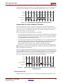
Performance Options and Data Port Parameters
This screen provides performance options and data port parameters for the core.
Figure 3-2:
FIFO Generator v3.3 User Guide
UG175 April 2, 2007
Performance Options and Data Port Parameters Screen
www.xilinx.com
31
R
Chapter 3: Generating the Core
Performance Options
Only available when Virtex-5 built-in FIFO or independent clock FIFO with block RAM or
distributed RAM FIFOs is selected. For more information, see “Read Operation,” page 46.
Standard FIFO
Implements a FIFO with standard latencies, and without using output registers.
First-word Fall-through FIFO
Implements a FIFO with registered outputs. For more information about FWFT
functionality, see “First-Word Fall-Through FIFO Read Operation,” page 48.
Data Port Parameters
Input Data Width
Valid range is 1 to 256.
Input Depth
Valid range is 16 to 4194394. Only depths with powers of 2 are allowed.
Output Data Width
Available if independent clocks configuration with block RAM is selected. Valid range
must comply with asymmetric port rules. See “Non-symmetric Aspect Ratios,” page 58.
Output Depth
Automatically calculated based on Input Data Width, Input Depth, and Output Data
Width.
Built-in FIFO Options
The Read Clock Frequency and Write Clock Frequency fields can be any integer from 1 to
1000. They are used to determine the optimal implementation of the domain-crossing logic
in the core. This option is only available for built-in FIFOs with independent clocks. If the
desired frequency is not within the allowable range, scale the read and write clock
frequencies so that they fit within the valid range, while maintaining their ratio
relationship.
The ECC feature enables built-in error correction in the Virtex-5 built-in FIFO macro. When
this feature is enabled, the built-in FIFO is set to the full ECC mode, where both the
encoder and decoder are enabled.
32
www.xilinx.com
FIFO Generator v3.3 User Guide
UG175 April 2, 2007
R
Optional Flags, Handshaking, and Initialization
Optional Flags, Handshaking, and Initialization
This screen allows you to select the optional status flags and set the handshaking options.
Figure 3-3:
Optional Flags, Handshaking, and Initialization Options Screen
Optional Flags
Almost Full Flag
Available in all FIFO implementations except those using Virtex-5 or Virtex-4 built-in
FIFOs. Generates an output port that indicates the FIFO is almost full (only one more word
can be written).
Almost Empty Flag
Available in all FIFO implementations except in those using Virtex-5 or Virtex-4 built-in
FIFOs. Generates an output port that indicates the FIFO is almost empty (only one more
word can be read).
Write Port Handshaking
Write Acknowledge
Generates write acknowledge flag which reports the status of a write operation. This signal
can be configured to be active high or low (default active high).
FIFO Generator v3.3 User Guide
UG175 April 2, 2007
www.xilinx.com
33
R
Chapter 3: Generating the Core
Overflow (Write Error)
Generates overflow flag which indicates when the previous write operation was not
successful. This signal can be configured to be active high or low (default active high).
Read Port Handshaking
Valid (Read Acknowledge)
Generates valid flag which indicates when the data on the output bus is valid. This signal
can be configured to be active high or low (default active high).
Underflow (Read Error)
Generates underflow flag to indicate that the previous read request was not successful.
This signal can be configured to be active high or low (default active high).
Initialization
Reset Pin
For FIFOs implemented with block RAM or distributed RAM, a reset pin is not required,
and the input pin is optional. For a common clock FIFO implemented using distributed or
block RAM, the user has the option to generate a synchronous or asynchronous reset.
34
www.xilinx.com
FIFO Generator v3.3 User Guide
UG175 April 2, 2007
R
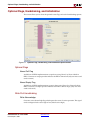
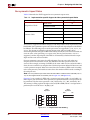
Programmable Flags
Programmable Flags
Use this screen to select the programmable flag type when generating a specific FIFO
Generator configuration.
Figure 3-4: Programmable Flags Screen
Programmable Flags
Programmable Full Type
Select a programmable full threshold type from the drop-down menu. The valid range for
each threshold is displayed, and will vary, depending on options selected elsewhere in the
GUI.
Full Threshold Assert Value
Available when Programmable Full with Single or Multiple Threshold Constants is
selected. Enter a user-defined value, or select a preset value from the drop-down menu.
The valid range for this threshold is provided in the GUI. When using a single threshold
constant, only the assert threshold value is used.
Full Threshold Negate Value
Available when Programmable Full with Multiple Threshold Constants is selected. Enter a
user-defined value, or select a preset value from the drop-down menu. The valid range for
this threshold is provided in the GUI.
FIFO Generator v3.3 User Guide
UG175 April 2, 2007
www.xilinx.com
35
R
Chapter 3: Generating the Core
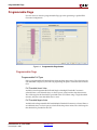
Programmable Empty Type
Select a programmable empty threshold type from the drop-down menu. The valid range
for each threshold is displayed, and will vary depending on options selected elsewhere in
the GUI.
Empty Threshold Assert Value
Available when Programmable Empty with Single or Multiple Threshold Constants is
selected. Enter a user-defined value, or select a preset value from the drop-down menu.
The valid range for this threshold is provided in the GUI. When using a single threshold
constant, only the assert value is used.
Empty Threshold Negate Value
Available when Programmable Empty with Multiple Threshold Constants is selected.
Enter a user-defined value, or select a preset value from the drop-down menu. The valid
range for this threshold is provided in the GUI.
Data Count and Reset
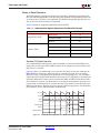
Use this screen to set data count and reset parameters.
Figure 3-5:
36
Data Count and Reset Screen
www.xilinx.com
FIFO Generator v3.3 User Guide
UG175 April 2, 2007
R
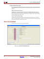
Summary
Data Count and Reset Options
Data Count
Use Extra Logic For More Accurate Data Counts
Only available for independent clocks FIFO with block RAM or distributed RAM, and
when using first-word fall-through. This option uses additional external logic to generate
a more accurate data count. See “First-Word Fall-Through Data Count,” page 57 for details.
Write Data Count
Available when an independent clocks FIFO with block RAM or distributed RAM is
selected. Valid range is from 1 to log2 (write depth).
Read Data Count
Available when an independent clocks FIFO with block RAM or distributed RAM is
selected. Valid range is from 1 to log2 (read depth).
Data Count
Available when a common clock FIFO with block RAM, distributed RAM or shift registers
is selected. Valid range is from 1 to log2 of input depth.
Resets
Dout Reset Value
Available in Virtex-II and newer architectures for all implementations using block RAM,
distributed RAM, or shift register memory. This text box indicates the hexidecimal value,
which is asserted on the output of the FIFO when RST is asserted.
Summary
This screen summarizes the FIFO type, dimensions, and any additional features selected.
In the Additional Features section, most features display either Not Selected (if the feature is
not used), or Selected (if the feature is used).
FIFO Generator v3.3 User Guide
UG175 April 2, 2007
www.xilinx.com
37
R
Chapter 3: Generating the Core
Note: Write depth and read depth provide the actual FIFO depths for the selected configuration.
These depths may differ slightly from the depth selected on page 2 of the FIFO GUI.
Figure 3-6:
38
Summary Screen
www.xilinx.com
FIFO Generator v3.3 User Guide
UG175 April 2, 2007
R
Chapter 4
Designing with the Core
This chapter describes the steps required to turn a FIFO Generator core into a fully
functioning design integrated with the user application logic. It is important to note that
depending on the configuration of the FIFO core, only a subset of the implementation
details provided are applicable. For successful use of a FIFO core, the design guidelines
discussed in this chapter must be observed.
General Design Guidelines
Know the Degree of Difficulty
A fully-compliant and feature-rich FIFO design is challenging to implement in any
technology. For this reason, it is important to understand that the degree of difficulty can
be significantly influenced by
•
Maximum system clock frequency
•
Targeted device architecture
•
Specific user application
Ensure that design techniques are used to facilitate implementation, including pipelining
and use of constraints (timing constraints, and placement and/or area constraints).
Understand Signal Pipelining and Synchronization
To understand the nature of FIFO designs, it is important to understand how pipelining is
used to maximize performance and implement synchronization logic for clock-domain
crossing. Data written into the write interface may take multiple clock cycles before it can
be accessed on the read interface.
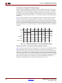
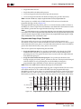
Synchronization Considerations
FIFOs with independent write and read clocks require that interface signals be used only in
their respective clock domains. The independent clocks FIFO handles all synchronization
requirements, enabling the user to cross between two clock domains that have no
relationship in frequency or phase.
Important: FIFO Full and Empty flags must be used to guarantee proper behavior.
Figure 4-1 shows the signals with respect to their clock domains. All signals are
synchronous to a specific clock, with the exception of RST, which performs an
asynchronous reset of the entire FIFO.
FIFO Generator v3.3 User Guide
UG175 April 2, 2007
www.xilinx.com
39
R
Chapter 4: Designing with the Core
.
DIN[N:0]
DOUT[M:0]
WR_EN
RD_EN
WR_CLK
RD_CLK
FULL
EMPTY
ALMOST_FULL
ALMOST_EMPTY
Write Clock
Domain
PROG_FULL
WR_ACK
Read Clock
Domain
PROG_EMPTY
VALID
OVERFLOW
UNDERFLOW
SBITERR
PROG_FULL_THRESH_ASSERT
DBITERR
PROG_FULL_THRESH_NEGATE
PROG_EMPTY_THRESH_ASSERT
PROG_FULL_THRESH
PROG_EMPTY_THRESH_NEGATE
PROG_EMPTY_THRESH
RST
Note: Optional ports represented in italics
Figure 4-1: FIFO with Independent Clocks: Write and Read Clock Domains
For write operations, the write enable signal (WR_EN) and data input (DIN) are
synchronous to WR_CLK. For read operations, the read enable (RD_EN) and data output
(DOUT) are synchronous to RD_CLK. All status outputs are synchronous to their respective
clock domains and can only be used in that clock domain. The performance of the FIFO can
be measured by independently constraining the clock period for the WR_CLK and RD_CLK
input signals.
The interface signals are evaluated on their rising clock edge (WR_CLK and RD_CLK). They
can be made falling-edge active (relative to the clock source) by inserting an inverter
between the clock source and the FIFO clock inputs. This inverter is absorbed into the
internal FIFO control logic and does not cause a decrease in performance or increase in
logic utilization.
Initializing the FIFO Generator
When designing with the built-in FIFO or common clock shift register FIFO, the FIFO must
be reset after the FPGA is configured and before operation begins. An asynchronous reset
pin (RST) is provided, which is an asynchronous reset that clears the internal counters and
output registers.
For FIFOs implemented with block RAM or distributed RAM, a reset is not required, and
the input pin is optional. For these FIFO configurations, users have the option of
asynchronous or synchronous reset (only in common clock implementations). When
asynchronous reset is implemented, it is synchronized to the clock domain in which it is
used to ensure that the FIFO initializes to a known state. This synchronization logic allows
for proper reset timing of the core logic, avoiding glitches and metastable behavior. For
independent clock implementations, the synchronization process mandates a 3-cycle delay
post-reset prior to writing to the FIFO. For common clock implementations, a 2-cycle delay
post-reset prior to writing to the FIFO is mandated. For synchronous reset, no additional
40
www.xilinx.com
FIFO Generator v3.3 User Guide
UG175 April 2, 2007
R
FIFO Implementations
synchronization is required and the FIFO is available for writing in the next cycle after
reset.
FIFO Implementations
Each FIFO configuration has a set of allowable features, as defined in Table 2-3, page 20.
Independent Clocks: Block RAM and Distributed RAM
Figure 4-2 illustrates the functional implementation of a FIFO configured with
independent clocks. This implementation uses block RAM or distributed RAM for
memory, counters for write and read pointers, conversions between binary and Gray code
for synchronization across clock domains, and logic for calculating the status flags.
Figure Top x-ref 1
WRITE CLOCK DOMAIN
READ CLOCK DOMAIN
EMPTY
ALMOST_EMPTY
Read Flag
Logic
PROG_EMPTY
RD_DATA_COUNT
Read Counter
Binary to Gray
Converter
Gray to Binary
Converter
MEMORY
WRITE PORT
Write Counter
ADDRA
WR_EN
READ PORT
DOUT
OPTIONAL
First Word Fall
Through Logic
WE
ADDRB
DIN
Read Counter
DOUT
RD_EN
DIN
Gray to Binary
Converters
Binary to Gray
Converters
Write Counter
FULL
ALMOST_FULL
PROG_FULL
Write Flag
Logic
WR_DATA_COUNT
Figure 4-2:
FIFO Generator v3.3 User Guide
UG175 April 2, 2007
Functional Implementation of a FIFO with Independent Clock Domains
www.xilinx.com
41
R
Chapter 4: Designing with the Core
This FIFO is designed to support an independent read clock (RD_CLK) and write clock
(WR_CLK); in other words, there is no required relationship between RD_CLK and WR_CLK
with regard to frequency or phase. The FIFO interface signals are only valid in their
respective clock domains and are summarize in Table 4-1.
Table 4-1:
Interface Signals and Corresponding Clock Domains
WR_CLK
RD_CLK
DIN
DOUT
WR_EN
RD_EN
FULL
EMPTY
ALMOST_FULL
ALMOST_EMPTY
PROG_FULL
PROG_EMPTY
WR_ACK
VALID
OVERFLOW
UNDERFLOW
WR_DATA_COUNT
RD_DATA_COUNT
For FIFO cores using independent clocks, the timing relationship between the write and
read operations and the status flags is affected by the relationship of the two clocks. For
example, the timing between writing to an empty FIFO and the deassertion of EMPTY is
determined by the phase and frequency relationship between the write and read clocks.
For additional information refer to the “Synchronization Considerations,” page 39.
Independent Clocks: Built-in FIFO
Figure 4-3 illustrates the functional implementation of FIFO configured with independent
clocks using the Virtex-5 built-in FIFO primitive. This design implementation consists of
cascaded built-in FIFO primitives and handshaking logic. The number of built-in
primitives depends on the FIFO width and depth requested.
The Virtex-4 built-in FIFO implementation allows generation of a single primitive. The
generated core includes a FIFO flag patch (defined in "Solution 1: Synchronous/Asynchronous
Clock Work-Arounds," in the Virtex-4 User Guide).
42
www.xilinx.com
FIFO Generator v3.3 User Guide
UG175 April 2, 2007
R
FIFO Implementations
WRITE DOMAIN
READ DOMAIN
Cascaded Built-in FIFO Primitives
FULL
EMPTY
RD_EN
WR_EN
WE
DIN
DIN
Built-In
FIFO
RE
DOUT
DOUT
SBITERR
DBITERR
WR_ACK
OVERFLOW
PROG_FULL
Logic For
Optional Flags:
Write Domain
UNDERFLOW
Logic For
Optional Flags:
Read Domain
Figure 4-3:
VALID
PROG_EMPTY
Functional Implementation of Built-in FIFO
This FIFO is designed to support an independent read clock (RD_CLK) and write clock
(WR_CLK); in other words, there is no required relationship between RD_CLK and WR_CLK
with regard to frequency or phase. The FIFO interface signals are only valid in their
respective clock domains, and are summarized in Table 4-2.
Table 4-2:
Interface Signals and Corresponding Clock Domains
WR_CLK
RD_CLK
DIN
DOUT
WR_EN
RD_EN
FULL
EMPTY
PROG_FULL
PROG_EMPTY
WR_ACK
VALID
OVERFLOW
UNDERFLOW
N/A
SBITERR
N/A
DBITERR
For FIFO cores using independent clocks, the timing relationship between the write and
read operations and the status flags is affected by the relationship of the two clocks. For
example, the timing between writing to an empty FIFO and the deassertion of EMPTY is
determined by the phase and frequency relationship between the write and read clocks.
For additional information, see “Synchronization Considerations,” page 39.
For Virtex-5 built-in FIFO configuration, the built-in ECC feature in the FIFO macro is
provided. For more information, see “Built-in Error Correction Checking,” page 60.
FIFO Generator v3.3 User Guide
UG175 April 2, 2007
www.xilinx.com
43
R
Chapter 4: Designing with the Core
Common Clock: Built-in FIFO
The FIFO Generator supports FIFO cores using the built-in FIFO primitive with a common
clock. This provides users the ability to use the built-in FIFO, while requiring only a single
clock interface. The behavior of the common clock configuration with built-in FIFO is
identical to the independent clock configuration with built-in FIFO, except all operations
are in relation to the common clock (CLK). See “Independent Clocks: Built-in FIFO,” page
42, for more information.
Common Clock FIFO: Block RAM and Distributed RAM
Figure 4-4 illustrates the functional implementation of a FIFO configured with a common
clock using block RAM or distributed RAM for memory. All signals are synchronous to a
single clock input (CLK). This design implements counters for write and read pointers and
logic for calculating the status flags. An optional synchronous (SRST) or asynchronous
(RST) reset signal is also available.
MEMORY
WRITE PORT
DIN
READ PORT
DIN
WR_EN
Write
Counter
DOUT
DOUT
WE
ADDRA
ADDRB
FULL
Read
Counter
RD_EN
EMPTY
Flag
Logic
ALMOST_FULL
PROG_FULL
ALMOST_EMPTY
PROG_EMPTY
DATA_COUNT
Figure 4-4: Functional Implementation of a Common Clock FIFO using Block RAM or
Distributed RAM
Common Clock FIFO: Shift Registers
Figure 4-5 illustrates the functional implementation of a FIFO configured with a common
clock using shift registers for memory. All operations are synchronous to the same clock
input (CLK). This design implements a single up/down counter for both the write and
read pointers and logic for calculating the status flags.
44
www.xilinx.com
FIFO Generator v3.3 User Guide
UG175 April 2, 2007
R
FIFO Usage and Control
MEMORY
WRITE PORT
DIN
WR_EN
READ PORT
DIN
DOUT
WE
RE
DOUT
RD_EN
ADDR
Pointer
Counter
FULL
EMPTY
Flag
Logic
ALMOST_FULL
PROG_FULL
ALMOST_EMPTY
PROG_EMPTY
DATA_COUNT
Figure 4-5: Functional Implementation of a Common Clock FIFO using Shift Registers
FIFO Usage and Control
Write Operation
This section describes the behavior of a FIFO write operation and the associated status
flags. When write enable is asserted and the FIFO is not full, data is added to the FIFO from
the input bus (DIN) and write acknowledge (WR_ACK) is asserted. If the FIFO is
continuously written to without being read, it fills with data. Write operations are only
successful when the FIFO is not full. When the FIFO is full and a write is initiated, the
request is ignored, the overflow flag is asserted and there is no change in the state of the
FIFO (overflowing the FIFO is non-destructive).
ALMOST_FULL and FULL Flags
Note: The Virtex-5 and Virtex-4 built-in FIFO does not support the ALMOST_FULL flag.
The almost full flag (ALMOST_FULL) indicates that only one more write can be performed
before FULL is asserted. This flag is active high and synchronous to the write clock
(WR_CLK).
The full flag (FULL) indicates that the FIFO is full and no more writes can be performed
until data is read out. This flag is active high and synchronous to the write clock (WR_CLK).
If a write is initiated when FULL is asserted, the write request is ignored and OVERFLOW is
asserted.
Important: For the Virtex-4 built-in FIFO implementation, the Full signal has an extra cycle
of latency. User Write Acknowledge to verify success or Programmable Full for an earlier
indication.
FIFO Generator v3.3 User Guide
UG175 April 2, 2007
www.xilinx.com
45
R
Chapter 4: Designing with the Core
Example Operation
Figure 4-6 shows a typical write operation. The user asserts WR_EN, causing a write
operation to occur on the next rising edge of the WR_CLK. Since the FIFO is not full,
WR_ACK is asserted, acknowledging a successful write operation. When only one
additional word can be written into the FIFO, the FIFO asserts the ALMOST_FULL flag.
When ALMOST_FULL is asserted, one additional write causes the FIFO to assert FULL.
When a write occurs after FULL is asserted, WR_ACK is deasserted and OVERFLOW is
asserted, indicating an overflow condition. Once the user performs one or more read
operations, the FIFO deasserts FULL, and data can successfully be written to the FIFO, as is
indicated by the assertion of WR_ACK and deassertion of OVERFLOW.
Note: The Virtex-4 built-in FIFO implementation shows an extra cycle of latency on the FULL flag.
WR_CLK
WR_EN
DIN
D1
D2
D3
D4
D5
D12
D13
FULL
ALMOST_FULL
WR_ACK
OVERFLOW
Figure 4-6:
Write Operation for a FIFO with Independent Clocks
Read Operation
This section describes the behavior of a FIFO read operation and the associated status
flags. When read enable is asserted and the FIFO is not empty, data is read from the FIFO
on the output bus (DOUT), and the valid flag (VALID) is asserted. If the FIFO is
continuously read without being written, the FIFO empties. Read operations are successful
when the FIFO is not empty. When the FIFO is empty and a read is requested, the read
operation is ignored, the underflow flag is asserted and there is no change in the state of
the FIFO (underflowing the FIFO is non-destructive).
ALMOST_EMPTY and EMPTY Flags
Note: The Virtex-5 and Virtex-4 built-in FIFO does not support the ALMOST_EMPTY flag.
The almost empty flag (ALMOST_EMPTY) indicates that the FIFO will be empty after one
more read operation. This flag is active high and synchronous to RD_CLK. This flag is
asserted when the FIFO has one remaining word that can be read.
The empty flag (EMPTY) indicates that the FIFO is empty and no more reads can be
performed until data is written into the FIFO. This flag is active high and synchronous to
the read clock (RD_CLK). If a read is initiated when EMPTY is asserted, the request is
ignored and UNDERFLOW is asserted.
Common Clock Note
When write and read operations occur simultaneously while EMPTY is asserted, the write
operation is accepted and the read operation is ignored. On the next clock cycle, EMPTY is
deasserted and UNDERFLOW is asserted.
46
www.xilinx.com
FIFO Generator v3.3 User Guide
UG175 April 2, 2007
R
FIFO Usage and Control
Modes of Read Operation
The FIFO Generator supports two modes of read options, standard read operation and
first-word fall-through (FWFT) read operation. The standard read operation provides the
user data on the cycle after it was requested. The FWFT read operation provides the user
data on the same cycle in which it is requested.
Table 4-3 details the supported implementations for FWFT.
Table 4-3:
Implementation-Specific Support for First-Word Fall-Through
FIFO Implementation
Independent Clocks
FWFT Support
Block RAM
✔
Distributed RAM
✔
Built-in
✔1
Block RAM
Distributed RAM
Common Clock
Shift Register
✔1
Built-in
1. Only supported in Virtex-5 built-in FIFO.
Standard FIFO Read Operation
For a standard FIFO read operation, after read enable is asserted and if the FIFO is not
empty, the next data stored in the FIFO is driven on the output bus (DOUT) and the valid
flag (VALID) is asserted.
Figure 4-7 shows a standard read access. Once the user writes at least one word into the
FIFO, EMPTY is deasserted—indicating data is available to be read. The user asserts
RD_EN, causing a read operation to occur on the next rising edge of RD_CLK. The FIFO
outputs the next available word on DOUT and asserts VALID, indicating a successful read
operation. When the last data word is read from the FIFO, the FIFO asserts EMPTY. If the
user continues to assert RD_EN while EMPTY is asserted, the read request is ignored, VALID
is deasserted, and UNDERFLOW is asserted. Once the user performs a write operation, the
FIFO deasserts EMPTY, allowing the user to resume valid read operations, as indicated by
the assertion of VALID and deassertion of UNDERFLOW.
RD_CLK
RD_EN
DOUT
D0
D1
D2
D3
VALID
UNDERFLOW
EMPTY
ALMOST_EMPTY
Figure 4-7: Standard Read Operation for a FIFO with Independent Clocks
FIFO Generator v3.3 User Guide
UG175 April 2, 2007
www.xilinx.com
47
R
Chapter 4: Designing with the Core
First-Word Fall-Through FIFO Read Operation
The first-word fall-through (FWFT) feature provides the ability to look-ahead to the next
word available from the FIFO without issuing a read operation. When data is available in
the FIFO, the first word falls through the FIFO and appears automatically on the output
bus (DOUT). Once the first word appears on DOUT, EMPTY is deasserted indicating one or
more readable words in the FIFO, and VALID is asserted, indicating a valid word is present
on DOUT.
Figure 4-8 shows a FWFT read access. Initially, the FIFO is not empty, the next available
data word is placed on the output bus (DOUT), and VALID is asserted. When the user
asserts RD_EN, the next rising clock edge of RD_CLK places the next data word onto DOUT.
After the last data word has been placed on DOUT, an additional read request by the user
causes the data on DOUT to become invalid, as indicated by the deassertion of VALID and
the assertion of EMPTY. Any further attempts to read from the FIFO results in an underflow
condition.
RD_CLK
RD_EN
DOUT
D0
D1
D2
D3
VALID
UNDERFLOW
EMPTY
ALMOST_EMPTY
Figure 4-8:
FWFT Read Operation for a FIFO with Independent Clocks
Common Clock FIFO, Simultaneous Read and Write Operation
Figure 4-9 shows atypical write and read operation. A write is issued to the FIFO, resulting
in the deassertion of the EMPTY flag. A simultaneous write and read is then issued,
resulting in no change in the status flags. Once two or more words are present in the FIFO,
the ALMOST_EMPTY flag is deasserted. Write requests are then issued to the FIFO, resulting
in the assertion of ALMOST_FULL when the FIFO can only accept one more write (without
a read). A simultaneous write and read is then issued, resulting in no change in the status
flags. Finally one additional write without a read results in the FIFO asserting FULL,
indicating no further data can be written until a read request is issued.
48
www.xilinx.com
FIFO Generator v3.3 User Guide
UG175 April 2, 2007
R
FIFO Usage and Control
CLK
WR_EN
RD_EN
EMPTY
ALMOST_EMPTY
FULL
ALMOST_FULL
Figure 4-9: Write and Read Operation for a FIFO with Common Clocks
Handshaking Flags
Handshaking flags (valid, underflow, write acknowledge and overflow) are supported to
provide additional information regarding the status of the write and read operations. The
handshaking flags are optional, and can be configured as active high or active low through
the CORE Generator GUI (see Handshaking Options in Chapter 4 for more information).
These flags (configured as active high) are illustrated in Figure 4-10.
Write Acknowledge
The write acknowledge flag (WR_ACK) is asserted at the completion of each successful
write operation and indicates that the data on the DIN port has been stored in the FIFO.
This flag is synchronous to the write clock (WR_CLK).
Valid
The operation of the valid flag (VALID) is dependent on the read mode of the FIFO. This
flag is synchronous to the read clock (RD_CLK).
Standard FIFO Read Operation
For standard read operation, the VALID flag is asserted at the rising edge of RD_CLK for
each successful read operation, and indicates that the data on the DOUT bus is valid. When
a read request is unsuccessful (when the FIFO is empty), VALID is not asserted.
FWFT FIFO Read Operation
For FWFT read operation, the VALID flag indicates the data on the output bus (DOUT) is
valid for the current cycle. A read request does not have to happen for data to be present
and valid, as the first-word fall-through logic automatically places the next data to be read
on the DOUT bus. VALID is asserted if there is one or more words in the FIFO. VALID is
deasserted when there are no more words in the FIFO.
Example Operation
Figure 4-10 illustrates the behavior of the FIFO flags. On the write interface, FULL is not
asserted and writes to the FIFO are successful (as indicated by the assertion of WR_ACK).
When a write occurs after FULL is asserted, WR_ACK is deasserted and OVERFLOW is
asserted, indicating an overflow condition. On the read interface, once the FIFO is not
EMPTY, the FIFO accepts read requests. In standard FIFO operation, VALID is asserted and
FIFO Generator v3.3 User Guide
UG175 April 2, 2007
www.xilinx.com
49
R
Chapter 4: Designing with the Core
DOUT is updated on the clock cycle following the read request. In FWFT operation, VALID
is asserted and DOUT is updated prior to a read request being issued. When a read request
is issued while EMPTY is asserted, VALID is deasserted and UNDERFLOW is asserted,
indicating an underflow condition.
Write Interface
WR_CLK
WR_EN
DIN
D1
D2
D3
WR_ACK
FULL
OVERFLOW
Standard Read Interface
RD_CLK
RD_EN
VALID
D1
DOUT
D2
D3
EMPTY
UNDERFLOW
FWFT Read Interface
RD_CLK
RD_EN
VALID
DOUT
D1
D2
D3
EMPTY
UNDERFLOW
Figure 4-10: Handshaking Signals for a FIFO with Independent Clocks
Underflow
The underflow flag (UNDERFLOW) is used to indicate that a read operation is unsuccessful.
This occurs when a read is initiated and the FIFO is empty. This flag is synchronous with
the read clock (RD_CLK). Underflowing the FIFO does not change the state of the FIFO (it
is non-destructive).
50
www.xilinx.com
FIFO Generator v3.3 User Guide
UG175 April 2, 2007
R
FIFO Usage and Control
Overflow
The overflow flag (OVERFLOW) is used to indicate that a write operation is unsuccessful.
This flag is asserted when a write is initiated to the FIFO while FULL is asserted. The
overflow flag is synchronous to the write clock (WR_CLK). Overflowing the FIFO does not
change the state of the FIFO (it is non-destructive).
Example Operation
Figure 4-11 illustrates the Handshaking flags. On the write interface, FULL is deasserted
and therefore writes to the FIFO are successful (indicated by the assertion of WR_ACK).
When a write occurs after FULL is asserted, WR_ACK is deasserted and OVERFLOW is
asserted, indicating an overflow condition. On the read interface, once the FIFO is not
EMPTY, the FIFO accepts read requests. Following a read request, VALID is asserted and
DOUT is updated. When a read request is issued while EMPTY is asserted, VALID is
deasserted and UNDERFLOW is asserted, indicating an underflow condition.
Write Interface
CLK
WR_EN
DIN
D1
D2
D3
WR_ACK
FULL
OVERFLOW
Read Interface
CLK
RD_EN
VALID
DOUT
D1
D2
D3
EMPTY
UNDERFLOW
Figure 4-11: Handshaking Signals for a FIFO with Common Clocks
Programmable Flags
The FIFO supports programmable flags to indicate that the FIFO has reached a userdefined fill level.
•
Programmable full (PROG_FULL) indicates that the FIFO has reached a user-defined
full threshold.
•
Programmable empty (PROG_EMPTY) indicates that the FIFO has reached a userdefined empty threshold.
FIFO Generator v3.3 User Guide
UG175 April 2, 2007
www.xilinx.com
51
R
Chapter 4: Designing with the Core
For these thresholds, the user can set a constant value or choose to have dedicated input
ports, enabling the thresholds to change dynamically in circuit. Hysteresis is also
optionally supported, by providing unique assert and negate values for each flag. Detailed
information about these options are provided below.
Programmable Full
The FIFO Generator supports four ways to define the programmable full threshold:
•
Single threshold constant
•
Single threshold with dedicated input port
•
Assert and negate threshold constants (provides hysteresis)
•
Assert and negate thresholds with dedicated input ports (provides hysteresis)
Note: The built-in FIFOs only support single-threshold constant programmable full.
These options are available in the CORE Generator GUI and accessed within the
programmable flags window (Figure 3-4).
The programmable full flag (PROG_FULL) is asserted when the number of entries in the
FIFO is greater than or equal to the user-defined assert threshold. When the programmable
full flag is asserted, the FIFO can continue to be written to until the full flag (FULL) is
asserted. If the number of words in the FIFO is less than the negate threshold, the flag is
deasserted.
Note: If a write operation occurs on a rising clock edge that causes the number of words to meet or
exceed the programmable full threshold, then the programmable full flag will assert on the next rising
clock edge. The deassertion of the programmable full flag has a longer delay, and depends on the
relationship between the write and read clocks.
Programmable Full: Single Threshold
This option enables the user to set a single threshold value for the assertion and
deassertion of PROG_FULL. When the number of entries in the FIFO is greater than or
equal to the threshold value, PROG_FULL is asserted. When the number of entries in the
FIFO is less than the threshold value, PROG_FULL is deasserted.
There are two options for implementing this threshold:
•
Single threshold constant. User specifies the threshold value through the CORE
Generator GUI. Once the core is generated, this value can only be changed by regenerating the core. This option consumes fewer resources than the single threshold
with dedicated input port.
•
Single threshold with dedicated input port. User specifies the threshold value
through an input port (PROG_FULL_THRESH) on the core. This input can be changed
while the FIFO is in reset, providing the user the flexibility to change the
programmable full threshold in-circuit without re-generating the core.
Note: Refer to the CORE Generator GUI for valid ranges for each threshold.
Figure 4-12 shows the programmable full flag with a single threshold. The user writes to
the FIFO until there are seven words in the FIFO. Since the programmable full threshold is
set to seven, the FIFO asserts PROG_FULL once seven words are written into the FIFO.
52
www.xilinx.com
FIFO Generator v3.3 User Guide
UG175 April 2, 2007
R
FIFO Usage and Control
Note that both write data count (WR_DATA_COUNT) and PROG_FULL have one clock cycle
of delay. Once the FIFO has six or fewer words in the FIFO, PROG_FULL is deasserted.
WR_CLK
WR_EN
WR_ACK
WR_DATA_COUNT
4
5
6
7
8
7
6
PROG_FULL
Figure 4-12: Programmable Full Single Threshold: Threshold Set to 7
Programmable Full: Assert and Negate Thresholds
This option enables the user to set separate values for the assertion and deassertion of
PROG_FULL. When the number of entries in the FIFO is greater than or equal to the assert
value, PROG_FULL is asserted. When the number of entries in the FIFO is less than the
negate value, PROG_FULL is deasserted.
There are two options for implementing these thresholds:
•
Assert and negate threshold constants: User specifies the threshold values through the
CORE Generator GUI. Once the core is generated, these values can only be changed
by re-generating the core. This option consumes fewer resources than the assert and
negate thresholds with dedicated input ports.
•
Assert and negate thresholds with dedicated input ports: User specifies the threshold
values through input ports on the core. These input ports can be changed while the
FIFO is in reset, providing the user the flexibility to change the values of the
programmable full assert (PROG_FULL_THRESH_ASSERT) and negate
(PROG_FULL_THRESH_NEGATE) thresholds in-circuit without re-generating the core.
Note: The full assert value must be larger than the full negate value. Refer to the CORE Generator
GUI for valid ranges for each threshold.
Figure 4-13 shows the programmable full flag with assert and negate thresholds. The user
writes to the FIFO until there are 10 words in the FIFO. Because the assert threshold is set
to 10, the FIFO then asserts PROG_FULL. The negate threshold is set to seven, and the FIFO
deasserts PROG_FULL once six words or fewer are in the FIFO. Both write data count
(WR_DATA_COUNT) and PROG_FULL have one clock cycle of delay.
WR_CLK
WR_EN
WR_ACK
WR_DATA_COUNT
8
9
10
9
8
7
6
PROG_FULL
Figure 4-13:
Programmable Full with Assert and Negate Thresholds: Assert Set to 10
and Negate Set to 7
Programmable Empty
The FIFO Generator supports four ways to define the programmable empty thresholds.
FIFO Generator v3.3 User Guide
UG175 April 2, 2007
www.xilinx.com
53
R
Chapter 4: Designing with the Core
•
Single threshold constant
•
Single threshold with dedicated input port
•
Assert and negate threshold constants (provides hysteresis)
•
Assert and negate thresholds with dedicated input ports (provides hysteresis)
Note: The built-in FIFOs only support single-threshold constant programmable full.
These options are available in the CORE Generator GUI and accessed within the
programmable flags window (Figure 3-4).
The programmable empty flag (PROG_EMPTY) is asserted when the number of entries in
the FIFO is less than or equal to the user-defined assert threshold. If the number of words
in the FIFO is greater than the negate threshold, the flag is deasserted.
Note: If a read operation occurs on a rising clock edge that causes the number of words in the FIFO
to be equal to or less than the programmable empty threshold, then the programmable empty flag will
assert on the next rising clock edge. The deassertion of the programmable empty flag has a longer
delay, and depends on the read and write clocks.
Programmable Empty: Single Threshold
This option enables the user to set a single threshold value for the assertion and
deassertion of PROG_EMPTY. When the number of entries in the FIFO is less than or equal
to the threshold value, PROG_EMPTY is asserted. When the number of entries in the FIFO is
greater than the threshold value, PROG_EMPTY is deasserted.
There are two options for implementing this threshold.
•
Single threshold constant: User specifies the threshold value through the CORE
Generator GUI. Once the core is generated, this value can only be changed by regenerating the core. This option consumes fewer resources than the single threshold
with dedicated input port.
•
Single threshold with dedicated input port: User specifies the threshold value
through an input port (PROG_EMPTY_THRESH) on the core. This input can be changed
while the FIFO is in reset, providing the user the flexibility to change the
programmable empty threshold in-circuit without re-generating the core.
Note: Refer to the CORE Generator GUI for valid ranges for each threshold.
Figure 4-14 shows the programmable empty flag with a single threshold. The user writes
to the FIFO until there are five words in the FIFO. Since the programmable empty
threshold is set to four, PROG_EMPTY is asserted until more than four words are present in
the FIFO. Once five words (or more) are present in the FIFO, PROG_EMPTY is deasserted.
Both read data count (RD_DATA_COUNT) and PROG_EMPTY have one clock cycle of delay.
RD_CLK
RD_EN
VALID
RD_DATA_COUNT
4
5
7
6
5
4
3
PROG_EMPTY
Figure 4-14:
54
Programmable Empty with Single Threshold: Threshold Set to 4
www.xilinx.com
FIFO Generator v3.3 User Guide
UG175 April 2, 2007
R
FIFO Usage and Control
Programmable Empty: Assert and Negate Thresholds
This option enables the user to set separate values for the assertion and deassertion of
PROG_EMPTY. When the number of entries in the FIFO is less than or equal to the assert
value, PROG_EMPTY is asserted. When the number of entries in the FIFO is greater than the
negate value, PROG_EMPTY is deasserted.
There are two options for implementing the assert and negate thresholds.
•
Assert and negate threshold constants. The threshold values are specified through
the CORE Generator GUI. Once the core is generated, these values can only be
changed by re-generating the core. This option consumes fewer resources than the
assert and negate thresholds with dedicated input ports.
•
Assert and negate thresholds with dedicated input ports. The threshold values are
specified through input ports on the core. These input ports can be changed while the
FIFO is in reset, providing the user the flexibility to change the values of the
programmable empty assert (PROG_EMPTY_THRESH_ASSERT) and negate
(PROG_EMPTY_THRESH_NEGATE) thresholds in-circuit without regenerating the core.
Note: The empty assert value must be less than the empty negate value. Refer to the CORE
Generator GUI for valid ranges for each threshold.
Figure 4-15 shows the programmable empty flag with assert and negate thresholds. The
user writes to the FIFO until there are eleven words in the FIFO. Since the programmable
empty deassert value is set to ten, PROG_EMPTY is deasserted when there are more than ten
words in the FIFO. Once the FIFO contains less than or equal to the programmable empty
negate value (set to seven), PROG_EMPTY is asserted. Both read data count
(RD_DATA_COUNT) and PROG_EMPTY have one clock cycle of delay.
RD_CLK
RD_EN
VALID
RD_DATA_COUNT
8
9
10
11
10
9
8
7
PROG_EMPTY
Figure 4-15: Programmable Empty with Assert and Negate Thresholds: Assert Set to 7 and
Negate Set to 10
Programmable Empty for First-Word Fall-Through
For FWFT FIFOs, PROG_EMPTY is guaranteed to be asserted when the number of words in
the FIFO is less than or equal to the programmable empty assert threshold. Under certain
conditions, it is possible for PROG_EMPTY to violate this rule, but only while EMPTY is
asserted. PROG_EMPTY should be assumed to be asserted whenever EMPTY is asserted.
Data Counts
DATA_COUNT tracks the number of words in the FIFO. You can specify the width of the
data count bus with a maximum width of log2 (FIFO depth). If the width specified is
smaller than the maximum allowable width, the bus is truncated by removing the lower
FIFO Generator v3.3 User Guide
UG175 April 2, 2007
www.xilinx.com
55
R
Chapter 4: Designing with the Core
bits. These signals are optional outputs of the FIFO Generator, and are enabled through the
CORE Generator GUI. Table 4-4 identifies FWFT support for each FIFO implementation.
Table 4-4:
Implementation-specific Support for Data Counts
FIFO Implementation
Independent Clocks
FWFT Support
Block RAM
✔
Distributed RAM
✔
Built-in
Common Clock
Block RAM
✔
Distributed RAM
✔
Shift Register
✔
Built-in
Read Data Count
Read data count (RD_DATA_COUNT) pessimistically reports the number of words available
for reading. The count is guaranteed to never over-report the number of words available in
the FIFO (although it may temporarily under-report the number of words available) to
ensure that the user never underflows the FIFO. The user can specify the width of the read
data count bus with a maximum width of log2 (read depth). If the width specified is
smaller than the maximum allowable width, the bus is truncated with the lower bits
removed.
For example, the user can specify to use two bits out of a maximum allowable three bits
(provided a FIFO depth of eight). These two bits indicate the number of words in the FIFO,
with a quarter resolution. This provides a status of the contents of the FIFO for the read
clock domain.
Note: If a read operation occurs on a rising clock edge of RD_CLK, that read is reflected on the
RD_DATA_COUNT signal following the next rising clock edge. A write operation on the WR_CLK clock
domain may take a number of clock cycles before being reflected in the RD_DATA_COUNT.
Write Data Count
Write data count (WR_DATA_COUNT) pessimistically reports the number of words written
into the FIFO. The count is guaranteed to never under-report the number of words in the
FIFO (although it may temporarily over-report the number of words present) to ensure
that the user never overflows the FIFO. The user can specify the width of the write data
count bus with a maximum width of log2 (write depth). If the width specified is smaller
than the maximum allowable width, the bus is truncated with the lower bits removed.
For example, you can only use two bits out of a maximum allowable three bits (provided a
FIFO depth of eight). These two bits indicate the number of words in the FIFO, with a
quarter resolution. This provides a status of the contents of the FIFO for the write clock
domain.
Note: If a write operation occurs on a rising clock edge of WR_CLK, that write will be reflected on the
WR_DATA_COUNT signal following the next rising clock edge. A read operation, which occurs on the
RD_CLK clock domain, may take a number of clock cycles before being reflected in the
WR_DATA_COUNT.
56
www.xilinx.com
FIFO Generator v3.3 User Guide
UG175 April 2, 2007
R
FIFO Usage and Control
First-Word Fall-Through Data Count
By providing the capability to read the next data word before requesting it, FWFT
implementations increase the depth of the FIFO. This depth increase causes the FWFT data
counts to be estimates of the number of words in the FIFO, not exact representations of the
number of words in the FIFO. By selecting “Use extra logic for more accurate Data Counts”
on page 4 of the CORE Generator GUI, an extra bit is added to WR_DATA_COUNT and
RD_DATA_COUNT to allow them to accurately express the full depth of the FIFO. When this
option is selected, RD_DATA_COUNT and WR_DATA_COUNT behave as described in the
sections above. When this option is not selected, the write and read data counts are only
estimates of the contents of the FIFO.
For example, an independent clocks FIFO with a user-selected input and output depth of
eight, has an actual depth (as reported on the summary page of the GUI) of seven. If FWFT
is selected, the additional register stages increase the FIFO’s effective depth to nine. In this
case, selecting “use extra logic for more accurate data counts” will increase the data count
counter sizes to display the full range of the FIFO (zero to nine words).
Note: For FWFT implementations, WR_DATA_COUNT is guaranteed to be accurate when words
are present in the FIFO, but may be incorrect by 2 at or near empty.
Example Operation
Figure 4-16 shows write and read data counts. When WR_EN is asserted and FULL is
deasserted, WR_DATA_COUNT increments. Similarly, when RD_EN is asserted and EMPTY is
deasserted, RD_DATA_COUNT decrements.
Note: In the first part of Figure 4-16, a successful write operation occurs on the third rising clock
edge, and is not reflected on WR_DATA_COUNT until the next full clock cycle is complete. Similarly,
RD_DATA_COUNT transitions one full clock cycle after a successful read operation.
Write Interface
WR_CLK
WR_EN
WR_DATA_COUNT
12
13
14
15
1
0
FULL
Read Interface
RD_CLK
RD_EN
RD_DATA_COUNT
3
2
EMPTY
Figure 4-16: Write and Read Data Counts for FIFO with Independent Clocks
FIFO Generator v3.3 User Guide
UG175 April 2, 2007
www.xilinx.com
57
R
Chapter 4: Designing with the Core
Non-symmetric Aspect Ratios
Table 4-5 identifies the FWFT support for non-symmetric aspect ratios.
Table 4-5:
Implementation-specific Support for Non-symmetric Aspect Ratios
FIFO Implementation
FWFT Support
✔
Block RAM
Independent Clocks
Distributed RAM
Built-in
Block RAM
Common Clock
Distributed RAM
Shift Register
Built-in
This feature is supported for FIFOs configured with independent clocks implemented with
block RAM. Non-symmetric aspect ratios allow the input and output depths of the FIFO to
be different. The following write-to-read aspect ratios are supported: 1:8, 1:4, 1:2, 1:1, 2:1,
4:1, 8:1. This feature is enabled by selecting unique write and read widths when
customizing the FIFO using the CORE Generator. By default, the write and read widths are
set to the same value (providing a 1:1 aspect ratio); but any ratio between 1:8 to 8:1 is
supported, and the output depth of the FIFO is automatically calculated from the input
depth and the write and read widths.
For non-symmetric aspect ratios, the full and empty flags are active only when one
complete word can be written or read. The FIFO does not allow partial words to be
accessed. For example, assuming a full FIFO, if the write width is 8 bits and read width is
2 bits, the user would have to complete four valid read operations before full deasserts and
a write operation accepted. Write data count shows the number of FIFO words according
to the write port ratio, and read data count shows the number of FIFO words according to
the read port ratio.
Note: For non-symmetric aspect ratios where the write width is smaller than the read width (1:8, 1:4,
1:2), the most significant bits are read first (refer to Figure 4-17 and Figure 4-18).
Figure 4-17 is an example of a FIFO with a 1:4 aspect ratio (write width = 2, read width = 8).
In this figure, four consecutive write operations are performed before a read operation can
be performed. The first write operation is “10”, followed by “11”, “00”, and finally “01.”
The memory is filling up from the right to the left (LSB to MSB). When a read operation is
performed, the received data is “01_00_11_10.”
Write
Operation
Read
Operation
MSB
Time
01
01
00
01
00
11
01
00
11
10
01
00
11
Figure 4-17:
58
01
LSB
00
11
10
10
1:4 Aspect Ratio: Data Ordering
www.xilinx.com
FIFO Generator v3.3 User Guide
UG175 April 2, 2007
R
FIFO Usage and Control
Figure 4-18 shows DIN, DOUT and the handshaking signals for a FIFO with a 1:4 aspect
ratio. After four words are written into the FIFO, EMPTY is deasserted. Then after a single
read operation, EMPTY is asserted again.
WR_CLK
WR_EN
DIN[1:0]
1
0
3
2
RD_CLK
RD_EN
DOUT[7:0]
4E
EMPTY
Figure 4-18:
1:4 Aspect Ratio: Status Flag Behavior
Figure 4-19 shows a FIFO with an aspect ratio of 4:1 (write width of 8, read width of 2). In
this example, a single write operation is performed, after which four read operations are
executed. The write operation is “11_00_01_11.” When a read operation is performed, the
data is received left to right (MSB to LSB). As shown, the first read results in data of “11”,
followed by “00”, “01”, and then “11.”
Write
Operation
MSB
11
Read
Operation
LSB
00
01
11
00
01
11
11
01
11
00
11
01
Time
11
Figure 4-19: 4:1 Aspect Ratio: Data Ordering
FIFO Generator v3.3 User Guide
UG175 April 2, 2007
www.xilinx.com
59
R
Chapter 4: Designing with the Core
Figure 4-20 shows DIN, DOUT, and the handshaking signals for a FIFO with an aspect ratio
of 4:1. After a single write, the FIFO deasserts EMPTY. Since no other writes occur, the FIFO
reasserts empty after four reads.
WR_CLK
WR_EN
DIN[7:0]
C7
RD_CLK
RD_EN
DOUT[1:0]
3
0
1
3
EMPTY
Figure 4-20:
4:1 Aspect Ratio: Status Flag Behavior
Built-in Error Correction Checking
Built-in ECC is supported for FIFOs configured with independent or common clock built-in
FIFOs targeting Virtex-5. When ECC is enabled, the built-in FIFO primitive used to create the
FIFO is configured in the full ECC mode (both encoder and decoder enabled), providing two
additional outputs to the FIFO Generator core: SBITERR and DBITERR. These outputs
indicate three possible read results: no error, single error corrected, and double error detected.
In the full ECC mode, the read operation does not correct the single error in the memory array,
it only presents corrected data on DOUT.
Figure 4-21 shows how the SBITERR and DBITERR outputs are generated in the FIFO
Generator core. The output signals are created by combining all the SBITERR and
DBITERR signals from the FIFO primitives using an OR gate. Because the FIFO primitives
may be cascaded in depth, when SBITERR or DBITERR is asserted, the error may have
occurred in any of the built-in FIFO macros chained in depth. Hence, these flags are not
correlated to the data currently being read from the FIFO Generator core or to a read
operation. For this reason, when the DBITERR is flagged, the user should assume that the
data in the entire FIFO has been corrupted and the user logic needs to take the appropriate
action. As an example, when DBITERR is flagged, an appropriate action for the user logic
is to halt all FIFO operation, reset the FIFO, and restart the data transfer.
The SBITERR and DBITERR outputs are not registered and are generated combinatorially.
If the configured FIFO uses two independent read and write clocks, the SBITERR and
DBITERR outputs may be generated from either the write or read clock domain. The
signals generated in the write clock domain are synchronized before being combined with
the SBITERR and DBITERR signals generated in the read clock domain.
Note that due to the differing read and write clock frequencies and the OR gate used to
combine the signals, the number of read clock cycles that the SBITERR and DBITERR flags
assert is not an accurate indicator of the number of errors found in the built-in FIFOs.
60
www.xilinx.com
FIFO Generator v3.3 User Guide
UG175 April 2, 2007
R
FIFO Usage and Control
Write Domain
Read Domain
Cascaded Built-in FIFO Primitives
DBITERR
SBITERR
FULL
EMPTY
WR_EN
WE
DIN
DIN
Built-In
FIFO
RE
DOUT
WR_ACK
OVERFLOW
RD_EN
DOUT
UNDERFLOW
Logic For Optional
Flags: Write Domain
PROG_FULL
Figure 4-21:
Logic For Optional
Flags: Read Domain
VALID
PROG_EMPTY
SBITERR and DBITERR Outputs in the FIFO Generator Core
Reset Behavior
The FIFO Generator provides a single reset input that resets all counters, output registers,
and memories when asserted. For block RAM or distributed RAM implementations,
resetting the FIFO is not required, and the reset pin can be disabled in the FIFO. There are
two reset options: asynchronous and synchronous.
Asynchronous Reset
The asynchronous reset (RST) input asynchronously resets all counters, output registers,
and memories when asserted. When reset is implemented, it is synchronized internally to
the core with each respective clock domain for setting the internal logic of the FIFO to a
known state. This synchronization logic allows for proper timing of the reset logic within
the core to avoid glitches and metastable behavior.
Due to the synchronization logic used, there is a latency in the deassertion of the FULL,
ALMOST_FULL, and PROG_FULL signals. Figure 4-23 illustrates the reset behavior for a
FIFO with an independent clock, and Figure 4-23 illustrates the reset behavior for a FIFO
with a common clock.
FIFO Generator v3.3 User Guide
UG175 April 2, 2007
www.xilinx.com
61
R
Chapter 4: Designing with the Core
WR_CLK
RST
FULL
ALMOST_FULL
PROG_FULL
Figure 4-22:
Synchronous Reset: FIFO with Independent Clock
CLK
RST
FULL
ALMOST_FULL
PROG_FULL
Figure 4-23:
Asynchronous Reset: FIFO with Common Clock
Table 4-6 defines the values of the output ports during power-up and the reset state. DOUT
reset value is supported for all architectures with the exception of Virtex and Spartan-II. If
the user does not specify a DOUT reset value, it defaults to 0. The FIFO requires a reset
pulse of only 1 clock cycle. FULL and ALMOST_FULL flags are asserted during reset to
ensure that no write operations occur, and handshaking signals are deasserted during
reset. Note that the power-up values for asynchronous reset are different than the reset
state value.
The FIFO requires a reset pulse of at least three clock cycles in length. Independent clock
FIFOs require four cycles post-reset prior to FIFO write availability—this is necessary for
proper reset synchronization. Common clock FIFOs, however, require three cycles after
reset prior to FIFO write availability. For the built-in FIFO, the RE_EN and WR_EN signal is
required to be deasserted during reset.
Table 4-6:
FIFO Reset Values
Signal
62
Block Memory
Distributed Memory
& Shift Register
Values
Built-in FIFO
Reset Values
Power-up
Values
DOUT
DOUT Reset Value
or 0 1
Content of
memory at
location 0
Same as reset
values
FULL
12
0
0
ALMOST FULL
12
N/A
0
www.xilinx.com
FIFO Generator v3.3 User Guide
UG175 April 2, 2007
R
FIFO Usage and Control
Table 4-6:
FIFO Reset Values (Continued)
EMPTY
1
0
1
ALMOST EMPTY
1
N/A
1
0 (active high) or
0 (active high) or
0 (active high) or
1 (active low)
1 (active low)
1 (active low)
0 (active high) or
0 (active high) or
0 (active high) or
1 (active low)
1 (active low)
0 (active high) or
0 (active high) or
0 (active high) or
1 (active low)
1 (active low)
1 (active low)
0 (active high) or
0 (active high) or
0 (active high) or
1 (active low)4
1 (active low)
1 (active low)
VALID
UNDERFLOW
1 (active
WR_ACK
OVERFLOW
low)3
PROG_FULL
12
0
0
PROG_EMPTY
1
1
1
RD_DATA_COUNT
0
N/A
0
WR_DATA_COUNT
0
N/A
0
1. The ability to set DOUT to a user-defined value is not available for block RAM implementations in Virtex, Spartan-II and
Spartan-IIE. DOUT resets to 0 when this feature is unavailable.
2. When reset is asserted, the FULL flags are asserted to prevent writes to the FIFO during reset.
3. The underflow signal is dependent on RD_EN. If RD_EN is asserted and the FIFO is empty, underflow is asserted.
4. The overflow signal is dependent on WR_EN. If WR_EN is asserted and the FIFO if full, overflow is asserted.
Synchronous Reset
The synchronous reset (SRST) input is only available for the Block and Distributed RAM
implementation of the common clock FIFO. It synchronously resets all counters, output
registers and memories when asserted. Because the reset pin is synchronous to the input
clock and there is only one clock domain in the FIFO, no additional synchronization logic
is necessary. Figure 4-24 illustrates the flags following the release of SRST.
CLK
SRST
FULL
ALMOST_FULL
PROG_FULL
Figure 4-24: Synchronous Reset: FIFO with a Common Clock
Table 4-7 defines the values of the output ports during power-up and the reset state. DOUT
reset value is supported for all architectures with the exception of Virtex and Spartan-II. If
the user does not specify a DOUT reset value, it defaults to 0. The FIFO requires a reset
pulse of only 1 clock cycle. The FIFOs are available for transaction on the clock cycle after
FIFO Generator v3.3 User Guide
UG175 April 2, 2007
www.xilinx.com
63
R
Chapter 4: Designing with the Core
the reset is released. The power-up values for the synchronous reset are the same as the
reset state.
Table 4-7:
FIFO Reset and Power-up Values
Block Memory and
Distributed Memory Values of
Output Ports During Reset and Power-up
Signal
DOUT
DOUT Reset Value or 01
FULL
0
ALMOST FULL
0
EMPTY
1
ALMOST EMPTY
1
VALID
0 (active high) or
1 (active low)
UNDERFLOW
0 (active high) or
1 (active low)2
WR_ACK
0 (active high) or
1 (active low)
OVERFLOW
0 (active high) or
1 (active low)3
PROG_FULL
0
PROG_EMPTY
0
RD_DATA_COUNT
0
WR_DATA_COUNT
0
1. The ability to set DOUT to a user-defined value is not available for block RAM implementations in Virtex, Spartan-II, and
Spartan-IIE. DOUT resets to 0 when this feature is unavailable.
2. The underflow signal is dependent on RD_EN. If RD_EN is asserted and the FIFO is empty, underflow is asserted.
3. The overflow signal is dependent on WR_EN. If WR_EN is asserted and the FIFO if full, overflow is asserted.
64
www.xilinx.com
FIFO Generator v3.3 User Guide
UG175 April 2, 2007
R
Chapter 5
Special Design Considerations
This chapter provides additional design considerations for using the FIFO Generator core.
Resetting the FIFO
The FIFO Generator must be reset after the FPGA is configured and before operation
begins. Two reset pins are available, asynchronous (RST) and synchronous (SRST), and
both clear the internal counters and output registers.
•
For asynchronous reset, internal to the core, RST is synchronized to the clock domain
in which it is used, to ensure that the FIFO initializes to a known state. This
synchronization logic allows for proper reset timing of the core logic, avoiding
glitches and metastable behavior.
•
For synchronous reset, because the reset pin is synchronous to the input clock and
there is only one clock domain in the FIFO, no additional synchronization logic is
needed.
The generated FIFO core will be initialized after reset to a known state. For details about
reset values and behavior, see “Reset Behavior” in Chapter 4 of this guide.
Continuous Clocks
The FIFO Generator is designed to work only with free-running write and read clocks.
Xilinx does not recommend controlling the core by manipulating RD_CLK and WR_CLK. If
this functionality is required to gate FIFO operation, we recommend using the write enable
(WR_EN) and read enable (RD_EN) signals.
Pessimistic Full and Empty
When independent clock domains are selected, the full flag (FULL, ALMOST_FULL) and
empty flag (EMPTY, ALMOST_EMPTY) are pessimistic flags. FULL and ALMOST_FULL are
synchronous to the write clock (WR_CLK) domain, while EMPTY and ALMOST_EMPTY are
synchronous to the read clock (RD_CLK) domain.
The full flags are considered pessimistic flags because they assume that no read operations
have taken place in the read clock domain. ALMOST_FULL is guaranteed to be asserted on
the rising edge of WR_CLK when there is only one available location in the FIFO, and FULL
is guaranteed to be asserted on the rising edge of WR_CLK when the FIFO is full. There may
be a number of clock cycles between a read operation and the deassertion of FULL. The
precise number of clock cycles for FULL to deassert is not predictable due to the crossing of
clock domains and synchronization logic.
The EMPTY flags are considered pessimistic flags because they assume that no write
operations have taken place in the write clock domain. ALMOST_EMPTY is guaranteed to be
FIFO Generator v3.3 User Guide
UG175 April 2, 2007
www.xilinx.com
65
R
Chapter 5: Special Design Considerations
asserted on the rising edge of RD_CLK when there is only one more word in the FIFO, and
EMPTY is guaranteed to be asserted on the rising edge of RD_CLK when the FIFO is empty.
There may be a number of clock cycles between a write operation and the deassertion of
EMPTY. The precise number of clock cycles for EMPTY to deassert is not predictable due to
the crossing of clock domains and synchronization logic.
See Chapter 4, “Designing with the Core,” for detailed information about the latency and
behavior of the full and empty flags.
Programmable Full and Empty
The programmable full (PROG_FULL) and programmable empty (PROG_EMPTY) flags
provide the user flexibility in specifying when the programmable flags assert and deassert.
These flags can be set either by constant value(s) or by input port(s). These signals differ
from the full and empty flags because they assert one (or more) clock cycle after the assert
threshold has been reached. These signals are deasserted some time after the negate
threshold has been passed. In this way, PROG_EMPTY and PROG_FULL are also considered
pessimistic flags. See “Programmable Flags” in Chapter 4 of this guide for more
information about the latency and behavior of the programmable flags.
Write Data Count and Read Data Count
When independent clock domains are selected, write data count (WR_DATA_COUNT) and
read data count (RD_DATA_COUNT) signals are provided as an indication of the number of
words in the FIFO relative to the write or read clock domains, respectively.
Consider the following when using the WR_DATA_COUNT or RD_DATA_COUNT ports.
•
The WR_DATA_COUNT and RD_DATA_COUNT outputs are not an instantaneous
representation of the number of words in the FIFO, but can instantaneously provide
an approximation of the number of words in the FIFO.
•
WR_DATA_COUNT and RD_DATA_COUNT may skip values from clock cycle to clock
cycle.
•
Using non-symmetric aspect ratios, or running clocks which vary dramatically in
frequency, will increase the disparity between the data count outputs and the actual
number of words in the FIFO.
Note: The WR_DATA_COUNT and RD_DATA_COUNT outputs will always be correct after some
period of time where RD_EN=0 and WR_EN=0 (generally, just a few clock cycles after read and write
activity stops).
See “Data Counts” in Chapter 4 of this guide for details about the latency and behavior of
the data count flags.
Setup and Hold Time Violations
When generating a FIFO with independent clock domains, the core internally
synchronizes the write and read clock domains. For this reason, setup and hold time
violations are expected on certain registers within the core. In simulation, warning
messages may be issued indicating these violations. If these warning messages are from
the FIFO Generator core, they can be safely ignored. The core is designed to properly
handle these conditions, regardless of the phase or frequency relationship between the
write and read clocks.
66
www.xilinx.com
FIFO Generator v3.3 User Guide
UG175 April 2, 2007
R
Chapter 6
Simulating Your Design
The FIFO Generator is provided as a Xilinx technology-specific netlist, and as a behavioral
or structural simulation model. This chapter provides instructions for simulating the FIFO
Generator in your design.
Simulation Models
The FIFO Generator supports two types of simulation models based on the Xilinx CORE
Generator system project options. The models are available in both VHDL and Verilog.
Both types of models are described in detail in this chapter.
To choose a model, do the following:
1.
Open the CORE Generator.
2.
Select Options from the Project drop-down list.
3.
Click the Generation tab.
4.
Choose to generate a behavioral model or a structural model.
Behavioral Models
Important! The behavioral models provided are designed to reproduce the behavior and
functionality of the FIFO Generator, but are not cycle-accurate models (except for the common
clock FIFO with block RAM, distributed RAM, or shift registers). If cycle accurate models are
required (and common clock FIFO with block RAM, distributed RAM or shift registers is not
selected), it is recommended to use the structural model.
The behavioral models are considered to be zero-delay models, as the modeled write-toread latency is nearly zero. The behavioral models are functionally correct, and will
represent the behavior of the configured FIFO, although the write-to-read latency and the
behavior of the status flags will differ from the actual implementation of the FIFO design.
To generate behavioral models, select Behavioral and VHDL or Verilog in the Xilinx CORE
Generator project options. Behavioral models are the default project options.
The following considerations apply to the behavioral models.
• Write operations always occur relative to the write clock (WR_CLK) or common clock
(CLK) domain, as do the corresponding handshaking signals.
• Read operations always occur relative to the read clock (RD_CLK) or common clock
(CLK) domain, as do the corresponding handshaking signals.
• The delay through the FIFO (write-to-read latency) will differ between the VHDL
model, the Verilog model, and the core.
• The deassertion of the status flags (full, almost full, programmable full, empty, almost
FIFO Generator v3.3 User Guide
UG175 April 2, 2007
www.xilinx.com
67
R
Chapter 6: Simulating Your Design
empty, programmable empty) will vary between the VHDL model, the Verilog model,
and the core.
Note: If independent clocks or common clocks with built-in FIFO is selected, it is strongly
recommended to use the structural model, as the behavioral model does not correctly model the
behavior of the status flags (full, programmable full, empty and programmable empty).
Structural Models
The structural models are designed to provide a more accurate model of FIFO behavior at
the cost of simulation time. These models will provide a closer approximation of cycle
accuracy across clock domains for asynchronous FIFOs. No asynchronous FIFO model can
be 100% cycle accurate as physical relationships between the clock domains, including
temperature, process, and frequency relationships, affect the domain crossing
indeterminately.
To generate structural models, select Structural and VHDL or Verilog in the Xilinx CORE
Generator project options.
Note: Simulation performance may be impacted when simulating the structural models compared to
the behavioral models
68
www.xilinx.com
FIFO Generator v3.3 User Guide
UG175 April 2, 2007
R
Appendix A
Performance Information
Resource Utilization and Performance
Performance and resource utilization for a FIFO varies depending on the configuration
and features selected when customizing the core. The tables below provide example FIFO
configurations and the maximum performance and resources required.
Table A-1 provides results for a FIFO configured without optional features. The
benchmarks were performed using Virtex-II 2v3000, Virtex-4 4vlx15 -11, and Virtex-5
5vlx50-2 target devices.
Table A-1:
Benchmarks: FIFO Configured without Optional Features
Resources
FIFO Type
Synchronous
FIFO
Depth x
Width
512 x 16
(Block RAM)
Synchronous
FIFO
4096 x 16
(Block RAM)
Synchronous
FIFO
(Distributed
RAM)
Synchronous
FIFO
(Distributed
RAM)
Independent
Clocks FIFO
(Block RAM
64 x 16
512 x 16
512x 16
Performance
(MHz)
LUTs
FFs
Block RAM
Shift
Register
Distributed
RAM
Virtex-5
350 MHz
62
45
1
0
0
Virtex-4
200 MHz
64
43
1
0
0
Virtex-II
175 MHz
64
43
1
0
0
Virtex-5
350 MHz
84
57
2
0
0
Virtex-4
225 MHz
80
55
4
0
0
Virtex-II
175 MHz
80
55
4
0
0
Virtex-5
475 MHz
48
61
0
0
32
Virtex-4
250 MHz
89
47
0
0
128
Virtex-II
225 MHz
89
47
0
0
128
Virtex-5
375 MHz
85
80
0
0
256
Virtex-4
200 MHz
340
59
0
0
1024
Virtex-II
150 MHz
340
59
0
0
1024
Virtex-5
350 MHz
105
124
1
0
0
Virtex-4
250 MHz
103
105
1
0
0
Virtex-II
200 MHz
103
105
1
0
0
Family
FIFO Generator v3.3 User Guide
UG175 February 15, 2007
www.xilinx.com
69
R
Table A-1:
Appendix A: Performance Information
Benchmarks: FIFO Configured without Optional Features (Continued)
Resources
FIFO Type
Independent
Clocks FIFO
(Block RAM)
Independent
Clocks FIFO
(Distributed
RAM
Independent
Clocks FIFO
(Distributed
RAM
Shift Register
FIFO
Shift Register
FIFO
Depth x
Width
4096 x 16
64 x 16
512 x 16
64 x 16
512 x 16
Performance
(MHz)
LUTs
FFs
Block RAM
Shift
Register
Distributed
RAM
Virtex-5
350 MHz
147
163
2
0
0
Virtex-4
250 MHz
134
138
4
0
0
Virtex-II
175 MHz
134
138
4
0
0
Virtex-5
475 MHz
76
104
0
0
32
Virtex-4
325 MHz
112
100
0
0
128
Virtex-II
225 MHz
112
100
0
0
128
Virtex-5
350 MHz
126
148
0
0
256
Virtex-4
225 MHz
382
139
0
0
1024
Virtex-II
150 MHz
382
139
0
0
1024
Virtex-5
450 MHz
59
50
0
32
0
Virtex-4
200 MHz
68
43
0
64
0
Virtex-II
150 MHz
68
43
0
64
0
Virtex-5
275 MHz
159
67
0
256
0
Virtex-4
200 MHz
312
82
0
512
0
Virtex-II
150 MHz
312
82
0
512
0
Family
Table A-2 provides results for FIFOs configured with multiple programmable thresholds.
The benchmarks were performed using Virtex-II 2v3000, Virtex-4 4vlx15 -11, and Virtex-5
5vlx50-2 target devices.
Table A-2:
Benchmarks: FIFO Configured with Multiple Programmable Thresholds
Resources
FIFO Type
Synchronous
FIFO
Depth x
Width
512 x 16
(Block RAM)
Synchronous
FIFO
4096 x 16
(Block RAM)
Synchronous
FIFO
(Distributed
RAM)
70
64 x 16
Performance
(MHz)
LUTs
FFs
Block RAM
Shift
Register
Distributed
RAM
Virtex-5
350 MHz
91
70
1
0
0
Virtex-4
200 MHz
109
68
1
0
0
Virtex-II
175 MHz
109
68
1
0
0
Virtex-5
350 MHz
124
88
2
0
0
Virtex-4
225 MHz
135
86
4
0
0
Virtex-II
175 MHz
135
86
4
0
0
Virtex-5
475 MHz
75
90
0
0
32
Virtex-4
250 MHz
112
66
0
0
128
Virtex-II
225 MHz
112
66
0
0
128
Family
www.xilinx.com
FIFO Generator v3.3 User Guide
UG175 February 15, 2007
R
Resource Utilization and Performance
Table A-2:
Benchmarks: FIFO Configured with Multiple Programmable Thresholds (Continued)
Resources
FIFO Type
Synchronous
FIFO
(Distributed
RAM)
Depth x
Width
512 x 16
Independent
Clocks FIFO
(Block RAM
512x 16
Independent
Clocks FIFO
(Block RAM)
4096 x 16
Independent
Clocks FIFO
(Distributed
RAM
64 x 16
Independent
Clocks FIFO
(Distributed
RAM
512 x 16
Shift Register
FIFO
Shift Register
FIFO
64 x 16
512 x 16
Performance
(MHz)
LUTs
FFs
Block RAM
Shift
Register
Distributed
RAM
Virtex-5
375 MHz
115
105
0
0
256
Virtex-4
200 MHz
370
84
0
0
1024
Virtex-II
150 MHz
370
84
0
0
1024
Virtex-5
350 MHz
132
143
1
0
0
Virtex-4
250 MHz
163
126
1
0
0
Virtex-II
200 MHz
163
126
1
0
0
Virtex-5
350 MHz
185
186
2
0
0
Virtex-4
250 MHz
214
165
4
0
0
Virtex-II
175 MHz
214
165
4
0
0
Virtex-5
475 MHz
96
123
0
0
32
Virtex-4
325 MHz
134
115
0
0
128
Virtex-II
225 MHz
134
115
0
0
128
Virtex-5
350 MHz
154
168
0
0
256
Virtex-4
225 MHz
412
160
0
0
1024
Virtex-II
150 MHz
412
160
0
0
1024
Virtex-5
450 MHz
68
63
0
32
0
Virtex-4
200 MHz
97
62
0
64
0
Virtex-II
150 MHz
97
62
0
64
0
Virtex-5
275 MHz
174
91
0
256
0
Virtex-4
200 MHz
355
106
0
512
0
Virtex-II
150 MHz
355
106
0
512
0
Family
Table A-3 provides results for FIFOs configured to use the Virtex-5 built-in FIFO. The
benchmarks were performed using a Virtex-5 5vlx50-2 target device.
Table A-3:
Benchmarks: FIFO Configured with Virtex-5 FIFO36 Resources
FIFO Type
Depth x Width
Resources
Performance
(MHz)
LUTs
FFs
FIFO36s
Standard
500
0
2
1
FWFT
400
2
4
1
Standard
350
10
6
4
FWFT
375
13
10
4
Read Mode
512 x 72
Synchronous FIFO36
(basic)
16k x 8
FIFO Generator v3.3 User Guide
UG175 February 15, 2007
www.xilinx.com
71
R
Table A-3:
Appendix A: Performance Information
Benchmarks: FIFO Configured with Virtex-5 FIFO36 Resources
FIFO Type
Depth x Width
Resources
Performance
(MHz)
LUTs
FFs
FIFO36s
Standard
500
2
6
1
FWFT
400
4
6
1
Standard
350
12
12
4
FWFT
375
16
13
4
Standard
500
0
2
1
FWFT
500
0
2
1
Standard
375
6
2
4
FWFT
375
6
2
4
Standard
500
2
6
1
FWFT
500
2
4
1
Standard
350
8
8
4
FWFT
350
9
5
4
Read Mode
512 x 72
Synchronous FIFO36
(with handshaking)
16k x 8
512 x 72
Independent Clocks
FIFO36 (basic)
16k x 8
Independent Clocks
FIFO36
(with handshaking)
512 x 72
16k x 8
Table A-4 provides results for FIFOs configured to use the Virtex-4 built-in FIFO with
patch. The benchmarks were performed using a Virtex-4 4vlx15 -11 target device
Benchmarks: FIFO Configured with Virtex-4 FIFO16 Patch
FIFO Type
Depth x
Width
Built-in FIFO (basic)
512 x 36
Built-in FIFO
(with handshaking)
512 x 36
72
Performance
(MHz)
Table A-4:
LUTs
WR_CLK ≥RD_CLK
375
110
129
72
1
RD_CLK > WR_CLK
400
92
115
72
1
WR_CLK ≥ RD_CLK
375
113
134
72
1
RD_CLK> WR_CLK
400
95
120
72
1
Clock Ratios
www.xilinx.com
Resources
FFs
Distributed
RAMs
FIFO16s
FIFO Generator v3.3 User Guide
UG175 February 15, 2007
R
Appendix B
Core Parameters
FIFO Parameters
Table B-1 describes the FIFO core parameters, including the XCO file value and the default
settings.
Table B-1:
FIFO Parameter Table
Parameter Name
XCO File Values
Default GUI Setting
Component_Name
instance_name
ASCII text starting with a letter and using the
following character set: a-z, 0-9, and _
fifo_generator_v3_3
FIFO Implementation
Common_Clock_Block_RAM
Common_Clock_Distributed_RAM
Common_Clock_Shift_Register
Common_Clock_Builtin_FIFO
Independent_Clocks_Block_RAM
Independent_Clocks_Distributed_RAM
Independent_Clocks_Builtin_FIFO
Common_Clock_Block_RAM
Input Data Width1
Integer in range 1 to 256
16
Output Data Width1
Integer in range 1 to 256
16
Input Depth1
2N where N is an integer 4 to 24
1024
2M
1024
Output
Depth1
where M is an integer 4 to 24
Data Count Width
Integer in range 1 to log2(Output Depth)
2
Read Clock Frequency
Integer 1 to 1000 (MHz)
100
Write Clock Frequency
Integer 1 to 1000 (MHz)
100
Almost Full Flag
true, false
false
Almost Empty Flag
true, false
false
Enable ECC
true, false
false
No_Programmable_Full_Threshold
No_Programmable_Full_Threshold
Programmable Full Type
Single_Programmable_Full_Threshold_Constant
Multiple_Programmable_Full_Threshold_Constants
Single_Programmable_Full_Threshold_Input_Port
Multiple_Programmable_Full_Threshold_Input_Ports
Full Threshold Assert Value
See range under Programmable Flags.
768
Full Threshold Negate Value
See range under “Programmable Flags,” page 51.
768
FIFO Generator v3.3 User Guide
UG175 April 2, 2007
www.xilinx.com
73
R
Table B-1:
Appendix B: Core Parameters
FIFO Parameter Table (Continued)
Parameter Name
Programmable Empty Type
XCO File Values
No_Programmable_Empty_Threshold
Default GUI Setting
No_Programmable_Empty_Threshold
Sigle_Programmable_Empty_Threshold_Constant
Multiple_Programmable_Empty_Threshold_Constants
Single_Programmable_Empty_Threshold_Input_Port
Multiple_Programmable_Empty_Threshold_Input_Ports
Empty Threshold Assert Value
See range under “Programmable Flags,” page 51.
256
Empty Threshold Negate Value
See range under “Programmable Flags,” page 51.
256
Write Acknowledge Flag
true, false
false
Write Acknowledge Sense
Active_High, Active_Low
Active_High
Overflow Flag
true, false
false
Overflow Sense
Active_High, Active_Low
Active_High
Valid Flag
true, false
false
Valid Sense
Active_High, Active_Low
Active_High
Underflow Flag
true, false
false
Underflow Sense
Active_High, Active_Low
Active_High
Dout Reset Value
Hex value in range of 0 to output data width - 1
0
Primitive Depth
512, 1024, 2048, 4096
1024
Read Data Count
true, false
false
Read Data Count Width
Integer in range 1 to log2(output depth)
10
Write Data Count
true, false
false
log2(input
Write Data Count Width
Integer in range 1 to
Data Count
true, false
false
Performance Options
First_Word_Fall_Through, Standard_Fifo
Standard_Fifo
Read Latency
integer range 0 to 1
1
Reset Pin
true, false
true
depth)
10
1. User customized core should not exceed the number of shift registers, built-in FIFOs, block RAM, or distributed RAM primitives available in the targeted architecture. It is the user’s responsibility to know the resource availability in the targeted device.
74
www.xilinx.com
FIFO Generator v3.3 User Guide
UG175 April 2, 2007