1
LogiCORE™ IP
FIFO Generator v5.1
User Guide
UG175 April 24, 2009
R
R
Xilinx is providing this product documentation, hereinafter “Information,” to you “AS IS” with no warranty of any kind, express or implied.
Xilinx makes no representation that the Information, or any particular implementation thereof, is free from any claims of infringement. You
are responsible for obtaining any rights you may require for any implementation based on the Information. All specifications are subject to
change without notice. XILINX EXPRESSLY DISCLAIMS ANY WARRANTY WHATSOEVER WITH RESPECT TO THE ADEQUACY OF
THE INFORMATION OR ANY IMPLEMENTATION BASED THEREON, INCLUDING BUT NOT LIMITED TO ANY WARRANTIES OR
REPRESENTATIONS THAT THIS IMPLEMENTATION IS FREE FROM CLAIMS OF INFRINGEMENT AND ANY IMPLIED WARRANTIES
OF MERCHANTABILITY OR FITNESS FOR A PARTICULAR PURPOSE. Except as stated herein, none of the Information may be copied,
reproduced, distributed, republished, downloaded, displayed, posted, or transmitted in any form or by any means including, but not limited
to, electronic, mechanical, photocopying, recording, or otherwise, without the prior written consent of Xilinx.
© 2005–2009 Xilinx, Inc. All rights reserved.
XILINX, the Xilinx logo, the Brand Window, and other designated brands included herein are trademarks of Xilinx, Inc. All other trademarks
are the property of their respective owners.
Revision History
The following table shows the revision history for this document.
Date
Version
Revision
04/28/05
1.1
Initial Xilinx release.
8/31/05
2.0
Updated guide for release v2.2, added SP3 to ISE v7.1i, incorporated edits from
engineering specific for this release, including FWFT, and Built-in FIFO flags, etc.
1/11/06
3.0
Updated for v2.3 release, ISE v8.1i.
7/13/06
4.0
Added Virtex-5 support, reorganized Chapter 5, added ISE v8.2i, version to 3.1
9/21/06
5.0
Core version updated to v3.2; support added for Spartan-3A.
2/15/07
6.0
Core version updated to 3.3; Xilinx tools updated to 9.1i.
4/02/07
6.5
Added support for Spartan-3A DSP devices.
8/8/07
6.6
Updated core to v4.1, ISE tools 9.2i, Cadence IUS v5.8.
10/10/07
7.0
Updated core to v4.2, IUS to v6.1, Xilinx trademark references.
3/24/08
8.0
Updated core to v4.3, ISE tools 10.1, Mentor Graphics® ModelSim® v6.3c.
9/19/08
9.0
Updated core to v4.4, ISE tools 10.1, SP3.
12/17/08
9.0.1
Early access documentation.
4/24/09
10.0
Updated core to v5.1, and ISE tools to v11.1.
FIFO Generator v5.1 User Guide
www.xilinx.com
UG175 April 24, 2009
Table of Contents
Preface: About This Guide
Guide Contents . . . . . . . . . . . . . . . . . . . . . . . . . . . . . . . . . . . . . . . . . . . . . . . . . . . . . . . . . . . . . 11
Conventions . . . . . . . . . . . . . . . . . . . . . . . . . . . . . . . . . . . . . . . . . . . . . . . . . . . . . . . . . . . . . . . . 12
Typographical . . . . . . . . . . . . . . . . . . . . . . . . . . . . . . . . . . . . . . . . . . . . . . . . . . . . . . . . . . . . 12
Online Document . . . . . . . . . . . . . . . . . . . . . . . . . . . . . . . . . . . . . . . . . . . . . . . . . . . . . . . . . 13
Chapter 1: Introduction
About the Core . . . . . . . . . . . . . . . . . . . . . . . . . . . . . . . . . . . . . . . . . . . . . . . . . . . . . . . . . . . . . .
Recommended Design Experience . . . . . . . . . . . . . . . . . . . . . . . . . . . . . . . . . . . . . . . . . . .
Technical Support . . . . . . . . . . . . . . . . . . . . . . . . . . . . . . . . . . . . . . . . . . . . . . . . . . . . . . . . . . .
Feedback. . . . . . . . . . . . . . . . . . . . . . . . . . . . . . . . . . . . . . . . . . . . . . . . . . . . . . . . . . . . . . . . . . . .
15
15
16
16
FIFO Generator . . . . . . . . . . . . . . . . . . . . . . . . . . . . . . . . . . . . . . . . . . . . . . . . . . . . . . . . . . . 16
Document . . . . . . . . . . . . . . . . . . . . . . . . . . . . . . . . . . . . . . . . . . . . . . . . . . . . . . . . . . . . . . . 16
Chapter 2: Core Overview
Feature Overview . . . . . . . . . . . . . . . . . . . . . . . . . . . . . . . . . . . . . . . . . . . . . . . . . . . . . . . . . . . 17
Clock Implementation Operation . . . . . . . . . . . . . . . . . . . . . . . . . . . . . . . . . . . . . . . . . . .
Virtex-6 and Virtex-5 FPGA Built-in FIFO Support . . . . . . . . . . . . . . . . . . . . . . . . . . . .
Virtex-4 FPGA Built-in FIFO Support . . . . . . . . . . . . . . . . . . . . . . . . . . . . . . . . . . . . . . . .
First-Word Fall-Through . . . . . . . . . . . . . . . . . . . . . . . . . . . . . . . . . . . . . . . . . . . . . . . . . . .
Memory Types . . . . . . . . . . . . . . . . . . . . . . . . . . . . . . . . . . . . . . . . . . . . . . . . . . . . . . . . . . .
Non-Symmetric Aspect Ratio . . . . . . . . . . . . . . . . . . . . . . . . . . . . . . . . . . . . . . . . . . . . . . .
Embedded Registers in block RAM and FIFO Macros . . . . . . . . . . . . . . . . . . . . . . . . . .
Error Injection and Correction . . . . . . . . . . . . . . . . . . . . . . . . . . . . . . . . . . . . . . . . . . . . . .
17
17
17
17
18
18
18
19
Core Configuration and Implementation . . . . . . . . . . . . . . . . . . . . . . . . . . . . . . . . . . . . 19
Common Clock: Block RAM, Distributed RAM, Shift Register . . . . . . . . . . . . . . . . . .
Common Clock: Virtex-6, VIrtex-5 or Virtex-4 FPGA Built-in FIFO . . . . . . . . . . . . . .
Independent Clocks: Block RAM and Distributed RAM . . . . . . . . . . . . . . . . . . . . . . . .
Independent Clocks: Built-in FIFO for Virtex-6, Virtex-5 or Virtex-4 FPGAs . . . . . . .
19
20
20
20
FIFO Generator Features . . . . . . . . . . . . . . . . . . . . . . . . . . . . . . . . . . . . . . . . . . . . . . . . . . . . 21
Using Block RAM FIFOs Instead of Built-in FIFOs . . . . . . . . . . . . . . . . . . . . . . . . . . 22
FIFO Interfaces. . . . . . . . . . . . . . . . . . . . . . . . . . . . . . . . . . . . . . . . . . . . . . . . . . . . . . . . . . . . . . 22
Interface Signals: FIFOs With Independent Clocks . . . . . . . . . . . . . . . . . . . . . . . . . . . . 22
Interface Signals: FIFOs with Common Clock . . . . . . . . . . . . . . . . . . . . . . . . . . . . . . . . . 27
Chapter 3: Generating the Core
CORE Generator Graphical User Interface . . . . . . . . . . . . . . . . . . . . . . . . . . . . . . . . . . . 31
FIFO Implementation . . . . . . . . . . . . . . . . . . . . . . . . . . . . . . . . . . . . . . . . . . . . . . . . . . . . . . . 32
Component Name . . . . . . . . . . . . . . . . . . . . . . . . . . . . . . . . . . . . . . . . . . . . . . . . . . . . . . . .
FIFO Implementation . . . . . . . . . . . . . . . . . . . . . . . . . . . . . . . . . . . . . . . . . . . . . . . . . . . . .
Common Clock (CLK), Block RAM . . . . . . . . . . . . . . . . . . . . . . . . . . . . . . . . . . . . . . . .
Common Clock (CLK), Distributed RAM . . . . . . . . . . . . . . . . . . . . . . . . . . . . . . . . . . . .
Common Clock (CLK), Shift Register . . . . . . . . . . . . . . . . . . . . . . . . . . . . . . . . . . . . . . .
FIFO Generator v5.1 User Guide
UG175 April 24, 2009
www.xilinx.com
32
32
33
33
33
3
R
Common Clock (CLK), Built-in FIFO . . . . . . . . . . . . . . . . . . . . . . . . . . . . . . . . . . . . . . .
Independent Clocks (RD_CLK, WR_CLK), Block RAM . . . . . . . . . . . . . . . . . . . . . . . . .
Independent Clocks (RD_CLK, WR_CLK), Distributed RAM . . . . . . . . . . . . . . . . . . . .
Independent Clocks (RD_CLK, WR_CLK), Built-in FIFO . . . . . . . . . . . . . . . . . . . . . . . .
33
33
33
33
Performance Options and Data Port Parameters . . . . . . . . . . . . . . . . . . . . . . . . . . . . . . 34
Read Mode . . . . . . . . . . . . . . . . . . . . . . . . . . . . . . . . . . . . . . . . . . . . . . . . . . . . . . . . . . . . . .
Standard FIFO. . . . . . . . . . . . . . . . . . . . . . . . . . . . . . . . . . . . . . . . . . . . . . . . . . . . . . . . .
First-Word Fall-Through FIFO . . . . . . . . . . . . . . . . . . . . . . . . . . . . . . . . . . . . . . . . . . . .
Built-in FIFO Options . . . . . . . . . . . . . . . . . . . . . . . . . . . . . . . . . . . . . . . . . . . . . . . . . . . . .
Read/Write Clock Frequencies . . . . . . . . . . . . . . . . . . . . . . . . . . . . . . . . . . . . . . . . . . . .
Data Port Parameters . . . . . . . . . . . . . . . . . . . . . . . . . . . . . . . . . . . . . . . . . . . . . . . . . . . . . .
Write Width . . . . . . . . . . . . . . . . . . . . . . . . . . . . . . . . . . . . . . . . . . . . . . . . . . . . . . . . . .
Write Depth . . . . . . . . . . . . . . . . . . . . . . . . . . . . . . . . . . . . . . . . . . . . . . . . . . . . . . . . . .
Read Width . . . . . . . . . . . . . . . . . . . . . . . . . . . . . . . . . . . . . . . . . . . . . . . . . . . . . . . . . . .
Read Depth . . . . . . . . . . . . . . . . . . . . . . . . . . . . . . . . . . . . . . . . . . . . . . . . . . . . . . . . . . .
Implementation Options . . . . . . . . . . . . . . . . . . . . . . . . . . . . . . . . . . . . . . . . . . . . . . . . . . .
Error Correction Checking in Block RAM or Built-in FIFO . . . . . . . . . . . . . . . . . . . . . .
Use Embedded Registers in Block RAM or FIFO . . . . . . . . . . . . . . . . . . . . . . . . . . . . . .
34
34
34
34
34
35
35
35
35
35
35
35
35
Optional Flags, Handshaking, and Initialization . . . . . . . . . . . . . . . . . . . . . . . . . . . . . 36
Optional Flags. . . . . . . . . . . . . . . . . . . . . . . . . . . . . . . . . . . . . . . . . . . . . . . . . . . . . . . . . . . .
Almost Full Flag . . . . . . . . . . . . . . . . . . . . . . . . . . . . . . . . . . . . . . . . . . . . . . . . . . . . . . .
Almost Empty Flag . . . . . . . . . . . . . . . . . . . . . . . . . . . . . . . . . . . . . . . . . . . . . . . . . . . . .
Handshaking Options . . . . . . . . . . . . . . . . . . . . . . . . . . . . . . . . . . . . . . . . . . . . . . . . . . . . .
Write Port Handshaking . . . . . . . . . . . . . . . . . . . . . . . . . . . . . . . . . . . . . . . . . . . . . . . . .
Read Port Handshaking . . . . . . . . . . . . . . . . . . . . . . . . . . . . . . . . . . . . . . . . . . . . . . . . .
Error Injection . . . . . . . . . . . . . . . . . . . . . . . . . . . . . . . . . . . . . . . . . . . . . . . . . . . . . . . . . . . .
Single Bit Error Injection . . . . . . . . . . . . . . . . . . . . . . . . . . . . . . . . . . . . . . . . . . . . . . . . .
Double Bit Error Injection . . . . . . . . . . . . . . . . . . . . . . . . . . . . . . . . . . . . . . . . . . . . . . . .
36
36
36
36
36
37
37
37
37
Initialization and Programmable Flags . . . . . . . . . . . . . . . . . . . . . . . . . . . . . . . . . . . . . . 38
Initialization . . . . . . . . . . . . . . . . . . . . . . . . . . . . . . . . . . . . . . . . . . . . . . . . . . . . . . . . . . . . .
Reset Pin . . . . . . . . . . . . . . . . . . . . . . . . . . . . . . . . . . . . . . . . . . . . . . . . . . . . . . . . . . . . .
Use Dout Reset . . . . . . . . . . . . . . . . . . . . . . . . . . . . . . . . . . . . . . . . . . . . . . . . . . . . . . . .
Programmable Flags . . . . . . . . . . . . . . . . . . . . . . . . . . . . . . . . . . . . . . . . . . . . . . . . . . . . . .
Programmable Full Type . . . . . . . . . . . . . . . . . . . . . . . . . . . . . . . . . . . . . . . . . . . . . . . .
Programmable Empty Type . . . . . . . . . . . . . . . . . . . . . . . . . . . . . . . . . . . . . . . . . . . . . .
38
38
38
39
39
39
Data Count. . . . . . . . . . . . . . . . . . . . . . . . . . . . . . . . . . . . . . . . . . . . . . . . . . . . . . . . . . . . . . . . . . 40
Data Count Options . . . . . . . . . . . . . . . . . . . . . . . . . . . . . . . . . . . . . . . . . . . . . . . . . . . . . . .
Use Extra Logic For More Accurate Data Counts . . . . . . . . . . . . . . . . . . . . . . . . . . . . . .
Data Count (Synchronized With Clk) . . . . . . . . . . . . . . . . . . . . . . . . . . . . . . . . . . . . . . .
Write Data Count (Synchronized with Write Clk) . . . . . . . . . . . . . . . . . . . . . . . . . . . . .
Read Data Count (Synchronized with Read Clk) . . . . . . . . . . . . . . . . . . . . . . . . . . . . . .
40
40
40
40
41
Summary . . . . . . . . . . . . . . . . . . . . . . . . . . . . . . . . . . . . . . . . . . . . . . . . . . . . . . . . . . . . . . . . . . . 41
Chapter 4: Designing with the Core
General Design Guidelines . . . . . . . . . . . . . . . . . . . . . . . . . . . . . . . . . . . . . . . . . . . . . . . . . 43
Know the Degree of Difficulty . . . . . . . . . . . . . . . . . . . . . . . . . . . . . . . . . . . . . . . . . . . . . . 43
Understand Signal Pipelining and Synchronization . . . . . . . . . . . . . . . . . . . . . . . . . . . 43
Synchronization Considerations . . . . . . . . . . . . . . . . . . . . . . . . . . . . . . . . . . . . . . . . . . . 43
Initializing the FIFO Generator . . . . . . . . . . . . . . . . . . . . . . . . . . . . . . . . . . . . . . . . . . . . . . 44
FIFO Implementations . . . . . . . . . . . . . . . . . . . . . . . . . . . . . . . . . . . . . . . . . . . . . . . . . . . . . . 45
Independent Clocks: Block RAM and Distributed RAM . . . . . . . . . . . . . . . . . . . . . . . . 45
4
www.xilinx.com
FIFO Generator v5.1 User Guide
UG175 April 24, 2009
R
Independent Clocks: Built-in FIFO . . . . . . . . . . . . . . . . . . . . . . . . . . . . . . . . . . . . . . . . . .
Common Clock: Built-in FIFO . . . . . . . . . . . . . . . . . . . . . . . . . . . . . . . . . . . . . . . . . . . . . .
Common Clock FIFO: Block RAM and Distributed RAM . . . . . . . . . . . . . . . . . . . . . . .
Common Clock FIFO: Shift Registers . . . . . . . . . . . . . . . . . . . . . . . . . . . . . . . . . . . . . . . .
47
48
49
49
FIFO Usage and Control . . . . . . . . . . . . . . . . . . . . . . . . . . . . . . . . . . . . . . . . . . . . . . . . . . . . . 50
Write Operation . . . . . . . . . . . . . . . . . . . . . . . . . . . . . . . . . . . . . . . . . . . . . . . . . . . . . . . . . .
ALMOST_FULL and FULL Flags . . . . . . . . . . . . . . . . . . . . . . . . . . . . . . . . . . . . . . . . . .
Example Operation . . . . . . . . . . . . . . . . . . . . . . . . . . . . . . . . . . . . . . . . . . . . . . . . . . . . .
Read Operation . . . . . . . . . . . . . . . . . . . . . . . . . . . . . . . . . . . . . . . . . . . . . . . . . . . . . . . . . .
ALMOST_EMPTY and EMPTY Flags . . . . . . . . . . . . . . . . . . . . . . . . . . . . . . . . . . . . . . .
Modes of Read Operation . . . . . . . . . . . . . . . . . . . . . . . . . . . . . . . . . . . . . . . . . . . . . . . .
Handshaking Flags . . . . . . . . . . . . . . . . . . . . . . . . . . . . . . . . . . . . . . . . . . . . . . . . . . . . . . .
Write Acknowledge . . . . . . . . . . . . . . . . . . . . . . . . . . . . . . . . . . . . . . . . . . . . . . . . . . . .
Valid . . . . . . . . . . . . . . . . . . . . . . . . . . . . . . . . . . . . . . . . . . . . . . . . . . . . . . . . . . . . . . . .
Example Operation . . . . . . . . . . . . . . . . . . . . . . . . . . . . . . . . . . . . . . . . . . . . . . . . . . . . .
Underflow . . . . . . . . . . . . . . . . . . . . . . . . . . . . . . . . . . . . . . . . . . . . . . . . . . . . . . . . . . . .
Overflow . . . . . . . . . . . . . . . . . . . . . . . . . . . . . . . . . . . . . . . . . . . . . . . . . . . . . . . . . . . . .
Example Operation . . . . . . . . . . . . . . . . . . . . . . . . . . . . . . . . . . . . . . . . . . . . . . . . . . . . .
Programmable Flags . . . . . . . . . . . . . . . . . . . . . . . . . . . . . . . . . . . . . . . . . . . . . . . . . . . . . .
Programmable Full . . . . . . . . . . . . . . . . . . . . . . . . . . . . . . . . . . . . . . . . . . . . . . . . . . . . .
Programmable Empty . . . . . . . . . . . . . . . . . . . . . . . . . . . . . . . . . . . . . . . . . . . . . . . . . . .
Data Counts . . . . . . . . . . . . . . . . . . . . . . . . . . . . . . . . . . . . . . . . . . . . . . . . . . . . . . . . . . . . .
Data Count (Common Clock FIFO Only) . . . . . . . . . . . . . . . . . . . . . . . . . . . . . . . . . . . .
Read Data Count (Independent Clock FIFO Only) . . . . . . . . . . . . . . . . . . . . . . . . . . . . .
Write Data Count (Independent Clock FIFO Only) . . . . . . . . . . . . . . . . . . . . . . . . . . . .
First-Word Fall-Through Data Count . . . . . . . . . . . . . . . . . . . . . . . . . . . . . . . . . . . . . . .
Example Operation . . . . . . . . . . . . . . . . . . . . . . . . . . . . . . . . . . . . . . . . . . . . . . . . . . . . .
Non-symmetric Aspect Ratios . . . . . . . . . . . . . . . . . . . . . . . . . . . . . . . . . . . . . . . . . . . . . .
Non-symmetric Aspect Ratio and First-Word Fall-Through . . . . . . . . . . . . . . . . . . . . .
Embedded Registers in block RAM and FIFO Macros
(Virtex-6, Virtex-5 and Virtex-4 FPGAs) . . . . . . . . . . . . . . . . . . . . . . . . . . . . . . . . . . .
Standard FIFOs . . . . . . . . . . . . . . . . . . . . . . . . . . . . . . . . . . . . . . . . . . . . . . . . . . . . . . . .
Block RAM Based FWFT FIFOs . . . . . . . . . . . . . . . . . . . . . . . . . . . . . . . . . . . . . . . . . . .
Built-in Based FWFT FIFOs (Common Clock Only) . . . . . . . . . . . . . . . . . . . . . . . . . . . .
Built-in Error Correction Checking . . . . . . . . . . . . . . . . . . . . . . . . . . . . . . . . . . . . . . . . . .
Built-in Error Injection . . . . . . . . . . . . . . . . . . . . . . . . . . . . . . . . . . . . . . . . . . . . . . . . . . . . .
Reset Behavior . . . . . . . . . . . . . . . . . . . . . . . . . . . . . . . . . . . . . . . . . . . . . . . . . . . . . . . . . . .
Asynchronous Reset (Enable Reset Synchronization Option is Selected) . . . . . . . . . . . .
Synchronous Reset . . . . . . . . . . . . . . . . . . . . . . . . . . . . . . . . . . . . . . . . . . . . . . . . . . . . .
50
50
51
51
51
52
54
54
54
55
56
57
57
57
58
60
62
63
63
63
64
66
66
69
70
70
70
70
71
72
73
73
77
Actual FIFO Depth . . . . . . . . . . . . . . . . . . . . . . . . . . . . . . . . . . . . . . . . . . . . . . . . . . . . . . . . . . 81
Block RAM, Distributed RAM and Shift RAM FIFOs . . . . . . . . . . . . . . . . . . . . . . . . . . 81
Virtex-6 and Virtex-5 FPGA Built-In FIFOs . . . . . . . . . . . . . . . . . . . . . . . . . . . . . . . . . . . 82
Virtex-4 FPGA Built-In FIFOs . . . . . . . . . . . . . . . . . . . . . . . . . . . . . . . . . . . . . . . . . . . . . . 82
Latency . . . . . . . . . . . . . . . . . . . . . . . . . . . . . . . . . . . . . . . . . . . . . . . . . . . . . . . . . . . . . . . . . . . . . 82
Non-Built-in FIFOs: Common Clock and Standard Read Mode Implementations . . 83
Non-Built-in FIFOs: Common CLock and FWFT Read Mode Implementations . . . . 84
Non-Built-in FIFOs: Independent Clock and Standard Read Mode Implementations86
Non-Built-in FIFOs: Independent Clock and FWFT Read Mode Implementations . 87
Virtex-6 and Virtex-5 FPGA Built-in FIFOs: Common Clock and Standard Read Mode
Implementations . . . . . . . . . . . . . . . . . . . . . . . . . . . . . . . . . . . . . . . . . . . . . . . . . . . . . . . 89
Virtex-6 and Virtex-5 FPGA Built-in FIFOs: Common Clock and FWFT Read Mode
Implementations . . . . . . . . . . . . . . . . . . . . . . . . . . . . . . . . . . . . . . . . . . . . . . . . . . . . . . . 90
FIFO Generator v5.1 User Guide
UG175 April 24, 2009
www.xilinx.com
5
R
Virtex-6 and Virtex-5 FPGA Built-in FIFOs: Independent Clocks and Standard Read Mode
Implementations . . . . . . . . . . . . . . . . . . . . . . . . . . . . . . . . . . . . . . . . . . . . . . . . . . . . . . . 91
Virtex-6 and Virtex-5 FPGA Built-in FIFOs: Independent Clocks and FWFT Read Mode
Implementations . . . . . . . . . . . . . . . . . . . . . . . . . . . . . . . . . . . . . . . . . . . . . . . . . . . . . . . 92
Chapter 5: Special Design Considerations
Resetting the FIFO . . . . . . . . . . . . . . . . . . . . . . . . . . . . . . . . . . . . . . . . . . . . . . . . . . . . . . . . . .
Continuous Clocks . . . . . . . . . . . . . . . . . . . . . . . . . . . . . . . . . . . . . . . . . . . . . . . . . . . . . . . . . .
Pessimistic Full and Empty . . . . . . . . . . . . . . . . . . . . . . . . . . . . . . . . . . . . . . . . . . . . . . . . . .
Programmable Full and Empty . . . . . . . . . . . . . . . . . . . . . . . . . . . . . . . . . . . . . . . . . . . . . .
Simultaneous Assertion of Full and Empty Flag . . . . . . . . . . . . . . . . . . . . . . . . . . . . .
Write Data Count and Read Data Count . . . . . . . . . . . . . . . . . . . . . . . . . . . . . . . . . . . . .
Setup and Hold Time Violations . . . . . . . . . . . . . . . . . . . . . . . . . . . . . . . . . . . . . . . . . . . .
95
95
95
96
96
97
97
Chapter 6: Simulating Your Design
Simulation Models . . . . . . . . . . . . . . . . . . . . . . . . . . . . . . . . . . . . . . . . . . . . . . . . . . . . . . . . . . 99
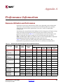
Appendix A: Performance Information
Resource Utilization and Performance . . . . . . . . . . . . . . . . . . . . . . . . . . . . . . . . . . . . . . 101
Appendix B: Core Parameters
FIFO Parameters . . . . . . . . . . . . . . . . . . . . . . . . . . . . . . . . . . . . . . . . . . . . . . . . . . . . . . . . . . . 105
6
www.xilinx.com
FIFO Generator v5.1 User Guide
UG175 April 24, 2009
Schedule of Figures
Preface: About This Guide
Chapter 1: Introduction
Chapter 2: Core Overview
Figure 2-1: FIFO with Independent Clocks: Interface Signals . . . . . . . . . . . . . . . . . . . . . . 22
Chapter 3: Generating the Core
Figure 3-1:
Figure 3-2:
Figure 3-3:
Figure 3-4:
Figure 3-5:
Figure 3-6:
Main FIFO Generator Screen . . . . . . . . . . . . . . . . . . . . . . . . . . . . . . . . . . . . . . . . .
Performance Options and Data Port Parameters Screen . . . . . . . . . . . . . . . . .
Optional Flags, Handshaking, and Initialization Options Screen. . . . . . . . .
Programmable Flags Screen . . . . . . . . . . . . . . . . . . . . . . . . . . . . . . . . . . . . . . . . . .
Data Count and Reset Screen. . . . . . . . . . . . . . . . . . . . . . . . . . . . . . . . . . . . . . . . .
Summary Screen. . . . . . . . . . . . . . . . . . . . . . . . . . . . . . . . . . . . . . . . . . . . . . . . . . . .
32
34
36
38
40
41
Chapter 4: Designing with the Core
Figure 4-1: FIFO with Independent Clocks: Write and Read Clock Domains . . . . . . . . . 44
Figure 4-2: Functional Implementation of a FIFO with Independent Clock Domains . 46
Figure 4-3: Functional Implementation of Built-in FIFO . . . . . . . . . . . . . . . . . . . . . . . . . . . 48
Figure 4-4: Functional Implementation of a Common Clock FIFO using
Block RAM or Distributed RAM . . . . . . . . . . . . . . . . . . . . . . . . . . . . . . . . . . . . . . . . . . . . . 49
Figure 4-5: Functional Implementation of a Common Clock FIFO using Shift Registers 50
Figure 4-6: Write Operation for a FIFO with Independent Clocks. . . . . . . . . . . . . . . . . . . 51
Figure 4-7: Standard Read Operation for a FIFO with Independent Clocks . . . . . . . . . . 53
Figure 4-8: FWFT Read Operation for a FIFO with Independent Clocks . . . . . . . . . . . . . 53
Figure 4-9: Write and Read Operation for a FIFO with Common Clocks . . . . . . . . . . . . . 54
Figure 4-10: Handshaking Signals for a FIFO with Independent Clocks . . . . . . . . . . . . . 56
Figure 4-11: Handshaking Signals for a FIFO with Common Clocks . . . . . . . . . . . . . . . . 57
Figure 4-12: Programmable Full Single Threshold: Threshold Set to 7. . . . . . . . . . . . . . . 59
Figure 4-13: Programmable Full with Assert and Negate Thresholds: Assert Set to 10
and Negate Set to 7 . . . . . . . . . . . . . . . . . . . . . . . . . . . . . . . . . . . . . . . . . . . . . . . . . . . . . . . . . 60
Figure 4-14: Programmable Empty with Single Threshold: Threshold Set to 4 . . . . . . . 61
Figure 4-15: Programmable Empty with Assert and Negate Thresholds: Assert Set to 7 and
Negate Set to 10 . . . . . . . . . . . . . . . . . . . . . . . . . . . . . . . . . . . . . . . . . . . . . . . . . . . . . . . . . . . . 62
Figure 4-16: Write and Read Data Counts for FIFO with Independent Clocks . . . . . . . . 66
Figure 4-17: 1:4 Aspect Ratio: Data Ordering . . . . . . . . . . . . . . . . . . . . . . . . . . . . . . . . . . . . . 67
Figure 4-18: 1:4 Aspect Ratio: Status Flag Behavior. . . . . . . . . . . . . . . . . . . . . . . . . . . . . . . . 68
Figure 4-19: 4:1 Aspect Ratio: Data Ordering . . . . . . . . . . . . . . . . . . . . . . . . . . . . . . . . . . . . . 68
Figure 4-20: 4:1 Aspect Ratio: Status Flag Behavior . . . . . . . . . . . . . . . . . . . . . . . . . . . . . . . 69
Figure 4-21: Standard Read Operation for a block RAM or built-in FIFO
with Use Embedded Registers Enabled . . . . . . . . . . . . . . . . . . . . . . . . . . . . . . . . . . . . . . . 70
FIFO Generator v5.1 User Guide
UG175 April 24, 2009
www.xilinx.com
7
R
Figure 4-22: FWFT Read Operation for a Synchronous Built-in
FIFO with User Embedded Registers Enabled . . . . . . . . . . . . . . . . . . . . . . . . . . . . . . . . .
Figure 4-23: Reset Value for Embedded Register. . . . . . . . . . . . . . . . . . . . . . . . . . . . . . . . . .
Figure 4-24: SBITERR and DBITERR Outputs in the FIFO Generator Core . . . . . . . . . .
Figure 4-25: Error Injection and Correction in Virtex-6 FPGA . . . . . . . . . . . . . . . . . . . . . .
Figure 4-26: Block RAM, Distributed RAM, Shift RAM with Full
Flags Reset Value of 1 . . . . . . . . . . . . . . . . . . . . . . . . . . . . . . . . . . . . . . . . . . . . . . . . . . . . . . .
Figure 4-27: Block RAM, Distributed RAM, Shift RAM with Full
Flags Reset Value of 0 . . . . . . . . . . . . . . . . . . . . . . . . . . . . . . . . . . . . . . . . . . . . . . . . . . . . . . .
Figure 4-28: Built-in FIFO, Asynchronous Reset Behavior . . . . . . . . . . . . . . . . . . . . . . . . .
Figure 4-29: Synchronous Reset: FIFO with a Common Clock . . . . . . . . . . . . . . . . . . . . . .
Figure 4-30: Synchronous Reset: FIFO with Independent Clock WR_RST then RD_RST . . . . . . . . . . . . . . . . . . . . . . . . . . . . . . . . . . . . . . . . . . . . . . . . . . . . .
Figure 4-31: Synchronous Reset: FIFO with Independent Clock RD_RST then WR_RST . . . . . . . . . . . . . . . . . . . . . . . . . . . . . . . . . . . . . . . . . . . . . . . . . . . . .
71
71
72
73
75
76
77
78
79
80
Chapter 5: Special Design Considerations
Chapter 6: Simulating Your Design
Appendix A: Performance Information
Appendix B: Core Parameters
8
www.xilinx.com
FIFO Generator v5.1 User Guide
UG175 April 24, 2009
Schedule of Tables
Preface: About This Guide
Chapter 1: Introduction
Chapter 2: Core Overview
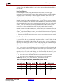
Table 2-1: Memory Configuration Benefits . . . . . . . . . . . . . . . . . . . . . . . . . . . . . . . . . . . . . . . 18
Table 2-2: FIFO Configurations . . . . . . . . . . . . . . . . . . . . . . . . . . . . . . . . . . . . . . . . . . . . . . . . . 19
Table 2-3: FIFO Configurations Summary. . . . . . . . . . . . . . . . . . . . . . . . . . . . . . . . . . . . . . . . 21
Table 2-4: Reset Signal for FIFOs with Independent Clocks . . . . . . . . . . . . . . . . . . . . . . . . 23
Table 2-5: Write Interface Signals for FIFOs with Independent Clocks . . . . . . . . . . . . . . 23
Table 2-6: Read Interface Signals for FIFOs with Independent Clocks. . . . . . . . . . . . . . . 25
Table 2-7: Interface Signals for FIFOs with a Common Clock . . . . . . . . . . . . . . . . . . . . . . 27
Chapter 3: Generating the Core
Chapter 4: Designing with the Core
Table 4-1: Interface Signals and Corresponding Clock Domains . . . . . . . . . . . . . . . . . . . . 47
Table 4-2: Interface Signals and Corresponding Clock Domains . . . . . . . . . . . . . . . . . . . . 48
Table 4-3: Implementation-Specific Support for First-Word Fall-Through . . . . . . . . . . . 52
Table 4-4: Implementation-specific Support for Data Counts. . . . . . . . . . . . . . . . . . . . . . . 63
Table 4-5: Empty FIFO WR_DATA_COUNT/DATA_COUNT Value . . . . . . . . . . . . . . . . 65
Table 4-6: Implementation-specific Support for Non-symmetric Aspect Ratios . . . . . . . 66
Table 4-7: FIFO Asynchronous Reset Values for block RAM, Distributed RAM,
and Shift RAM FIFOs . . . . . . . . . . . . . . . . . . . . . . . . . . . . . . . . . . . . . . . . . . . . . . . . . . . . . . . 74
Table 4-8: Asynchronous FIFO Reset Values for Built-in FIFO . . . . . . . . . . . . . . . . . . . . . 77
Table 4-9: Synchronous FIFO Reset and Power-up Values . . . . . . . . . . . . . . . . . . . . . . . . . 80
Table 4-10: Write Port Flags Update Latency Due to Write Operation . . . . . . . . . . . . . . . 83
Table 4-11: Read Port Flags Update Latency Due to Read Operation . . . . . . . . . . . . . . . . 83
Table 4-12: Write Port Flags Update Latency Due to Read Operation . . . . . . . . . . . . . . . . 83
Table 4-13: Read Port Flags Update Latency Due to Write Operation . . . . . . . . . . . . . . . . 84
Table 4-14: Write Port Flags Update Latency due to Write Operation . . . . . . . . . . . . . . . . 84
Table 4-15: Read Port Flags Update Latency due to Read Operation . . . . . . . . . . . . . . . . . 84
Table 4-16: Write Port Flags Update Latency Due to Read Operation . . . . . . . . . . . . . . . . 85
Table 4-17: Read Port Flags Update Latency Due to Write Operation . . . . . . . . . . . . . . . . 86
Table 4-18: Write Port Flags Update Latency Due to a Write Operation . . . . . . . . . . . . . . 86
Table 4-19: Read Port Flags Update Latency Due to a Read Operation . . . . . . . . . . . . . . . 86
Table 4-20: Write Port Flags Update Latency Due to a Read Operation . . . . . . . . . . . . . . 87
Table 4-21: Read Port Flags Update Latency Due to a Write Operation . . . . . . . . . . . . . . 87
FIFO Generator v5.1 User Guide
UG175 April 24, 2009
www.xilinx.com
9
R
Table 4-22: Write Port Flags Update Latency Due to a Write Operation . . . . . . . . . . . . . . 87
Table 4-23: Read Port Flags Update Latency Due to a Read Operation . . . . . . . . . . . . . . . 88
Table 4-24: Write Port Flags Update Latency Due to a Read Operation . . . . . . . . . . . . . . 88
Table 4-25: Read Port Flags Update Latency Due to a Write Operation . . . . . . . . . . . . . . 88
Table 4-26: Write Port Flags Update Latency Due to Write Operation. . . . . . . . . . . . . . . . 89
Table 4-27: Read Port Flags Update Latency Due to Read Operation . . . . . . . . . . . . . . . . 89
Table 4-28: Write Port Flags Update Latency Due to Read Operation . . . . . . . . . . . . . . . . 89
Table 4-29: Read Port Flags Update Latency Due to Write Operation . . . . . . . . . . . . . . . . 90
Table 4-30: Write Port Flags Update Latency Due to Write Operation. . . . . . . . . . . . . . . . 90
Table 4-31: Read Port Flags Update Latency Due to a Read Operation . . . . . . . . . . . . . . . 90
Table 4-32: Write Port Flags Update Latency Due to a Read Operation . . . . . . . . . . . . . . 90
Table 4-33: Read Port Flags Update Latency Due to a Write Operation . . . . . . . . . . . . . . 91
Table 4-34: Write Port Flags Update Latency Due to a Write Operation . . . . . . . . . . . . . . 91
Table 4-35: Read Port Flags Update Latency Due to a Read Operation . . . . . . . . . . . . . . . 92
Table 4-36: Write Port Flags Update Latency Due to a Read Operation . . . . . . . . . . . . . . 92
Table 4-37: Read Port Flags Update Latency Due to a Write Operation . . . . . . . . . . . . . . 92
Table 4-38: Write Port Flags Update Latency Due to a Write Operations . . . . . . . . . . . . . 92
Table 4-39: Read Port Flags Update Latency Due to a Read Operation . . . . . . . . . . . . . . . 93
Table 4-40: Write Port Flags Update Latency Due to a Read Operation . . . . . . . . . . . . . . 93
Table 4-41: Read Port Flags Update Latency Due to a Write Operation . . . . . . . . . . . . . . 93
Chapter 5: Special Design Considerations
Chapter 6: Simulating Your Design
Appendix A: Performance Information
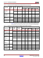
Table A-1: Benchmarks: FIFO Configured without Optional Features . . . . . . . . . . . . . . 101
Table A-2: Benchmarks: FIFO Configured with Multiple Programmable Thresholds 102
Table A-3: Benchmarks: FIFO Configured with Virtex-5 FIFO36 Resources. . . . . . . . . 103
Table A-4: Benchmarks: FIFO Configured with Virtex-4 FIFO16 Patch . . . . . . . . . . . . . 104
Appendix B: Core Parameters
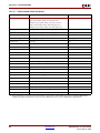
Table B-1: FIFO Parameter Table . . . . . . . . . . . . . . . . . . . . . . . . . . . . . . . . . . . . . . . . . . . . . . . 105
10
www.xilinx.com
FIFO Generator v5.1 User Guide
UG175 April 24, 2009
R
Preface
About This Guide
The LogicCORE™ IP FIFO Generator User Guide describes the function and operation of the
FIFO Generator, as well as information about designing, customizing, and implementing
the core.
Guide Contents
The following chapters are included:
•
“Preface, About this Guide” describes how the user guide is organized and the
conventions used in this guide.
•
Chapter 1, “Introduction,” describes the core and related information, including
recommended design experience, additional resources, technical support, and
submitting feedback to Xilinx.
•
Chapter 2, “Core Overview,” describes the core configuration options and their
interfaces.
•
Chapter 3, “Generating the Core,” describes how to generate the core using the Xilinx
CORE Generator Graphical User Interface (GUI).
•
Chapter 4, “Designing with the Core,” discusses how to use the core in a user
application.
•
Chapter 5, “Special Design Considerations,” discusses specific design features that
must be considered when designing with the core.
•
Chapter 6, “Simulating Your Design,” provides instructions for simulating the design
with either behavioral or structural simulation models.
•
Appendix A, “Performance Information,” provides a summary of the core’s
performance data.
•
Appendix B, “Core Parameters,” provides a comprehensive list of the parameters set
by the CORE Generator GUI for the FIFO Generator.
FIFO Generator v5.1 User Guide
UG175 April 24, 2009
www.xilinx.com
11
R
Preface:
Conventions
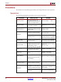
This document uses the following conventions. An example illustrates each convention.
Typographical
The following typographical conventions are used in this document:
Convention
Meaning or Use
Courier font
Messages, prompts, and
program files that the system
displays and signal names
speed grade: - 100
Courier bold
Literal commands you enter in
a syntactical statement
ngdbuild design_name
Angle brackets < >
Variables in a syntax
statement for which you must
supply values
<design_name>
References to other manuals
See the FIFO Generator Data
Sheet for details.
Emphasis in text
If a wire is drawn so that it
overlaps the pin of a symbol,
the two nets are not connected.
Dark Shading
Items that are not supported
or reserved items
This feature is not supported
Square brackets
An optional entry or
parameter. However, in bus
specifications, such as
bus[7:0], they are required.
ngdbuild [option_name]
design_name
A list of items from which you
must choose one or more
lowpwr ={on|off}
Separates items in a list of
choices
lowpwr ={on|off}
Vertical ellipsis
.
.
.
Repetitive material that has
been omitted
IOB #1: Name = QOUT’
IOB #2: Name = CLKIN’
.
.
.
Horizontal ellipsis . . .
Omitted repetitive material
allow block block_name
loc1 loc2 ... locn;
The prefix ‘0x’ or the suffix ‘h’
indicate hexadecimal notation
A read of address
0x00112975 returned
45524943h.
An ‘_n’ means the signal is
active low
usr_teof_n is active low.
Italic font
Braces
[ ]
{ }
Vertical bar
Notations
12
Example
|
www.xilinx.com
FIFO Generator v5.1 User Guide
UG175 April 24, 2009
R
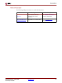
Conventions
Online Document
The following linking conventions are used in this document:
Convention
Meaning or Use
Blue text
Cross-reference link to a
location in the current
document
Blue, underlined text
Hyperlink to a website (URL)
FIFO Generator v5.1 User Guide
UG175 April 24, 2009
www.xilinx.com
Example
See “Additional Resources”
for more information.
Go to www.xilinx.com for the
latest speed files.
13
R
Preface:
14
www.xilinx.com
FIFO Generator v5.1 User Guide
UG175 April 24, 2009
R
Chapter 1
Introduction
The FIFO Generator core is a fully verified first-in first-out memory queue for use in any
application requiring in-order storage and retrieval, enabling high-performance and areaoptimized designs. This core can be customized using the Xilinx CORE Generator™
system as a complete solution with control logic already implemented, including
management of the read and write pointers and the generation of status flags.
This chapter introduces the FIFO Generator and provides related information, including
recommended design experience, additional resources, technical support, and submitting
feedback to Xilinx.
About the Core
The FIFO Generator is a Xilinx CORE Generator IP core, included in the latest IP Update on
the Xilinx IP Center. The core is free of charge and no license is required. For detailed
information about the core, see the FIFO Generator product page.
Windows
•
Windows XP® Professional 32-bit/64-bit
•
Windows Vista® Business 32-bit/64-bit
Linux
•
Red Hat® Enterprise WS 4.0 32-bit/64-bit
•
Red Hat Enterprise Desktop 5.0 32-bit/64-bit (with Workstation option)
•
SUSE Linux Enterprise (SLE) v10.1 32-bit/64-bit
Software
•
ISE® v11.1
Recommended Design Experience
The FIFO Generator is a fully verified solution, and can be used by all levels of design
engineers.
Important: When implementing a FIFO with independent write and read clocks, special
care must be taken to ensure the FIFO Generator is correctly used. “Synchronization
Considerations,” page 43 provides important information to help ensure correct design
configuration.
Similarly, asynchronous designs should also be aware that the behavioral models are not
cycle-accurate across clock domains. See Chapter 6, “Simulating Your Design,” for details.
FIFO Generator v5.1 User Guide
UG175 April 24, 2009
www.xilinx.com
15
R
Chapter 1: Introduction
Technical Support
For technical support, visit www.support.xilinx.com/. Questions are routed to a team of
engineers with FIFO Generator expertise.
Xilinx will provide technical support for use of this product as described in the LogiCORE
FIFO Generator User Guide. Xilinx cannot guarantee timing, functionality, or support of this
product for designs that do not follow these guidelines.
Feedback
Xilinx welcomes comments and suggestions about the FIFO Generator and the
documentation supplied with the core.
FIFO Generator
For comments or suggestions about the FIFO Generator, please submit a WebCase from
www.support.xilinx.com/. Be sure to include the following information:
•
Product name
•
Core version number
•
Explanation of your comments
Document
For comments or suggestions about this document, please submit a WebCase from
www.support.xilinx.com/. Be sure to include the following information:
16
•
Document title
•
Document number
•
Page number(s) to which your comments refer
•
Explanation of your comments
www.xilinx.com
FIFO Generator v5.1 User Guide
UG175 April 24, 2009
R
Chapter 2
Core Overview
This chapter provides an overview of the FIFO Generator configuration options and
interfaces.
Feature Overview
Clock Implementation Operation
The FIFO Generator enables FIFOs to be configured with either independent or common
clock domains for write and read operations. The independent clock configuration of the
FIFO Generator enables the user to implement unique clock domains on the write and read
ports. The FIFO Generator handles the synchronization between clock domains, placing no
requirements on phase and frequency relationships between clocks. A common clock
domain implementation optimizes the core for data buffering within a single clock
domain.
Virtex-6 and Virtex-5 FPGA Built-in FIFO Support
The FIFO Generator supports the Virtex®-6 and Virtex-5 FPGA built-in FIFO modules,
enabling the creation of large FIFOs by cascading the built-in FIFOs in both width and
depth. The core expands the capabilities of the built-in FIFOs by utilizing the FPGA fabric
to create optional status flags not implemented in the built-in FIFO macro. The built-in
Error Injection and Correction Checking (ECC) feature in the built-in FIFO macro is also
available.
Virtex-4 FPGA Built-in FIFO Support
The FIFO Generator supports a single instantiation of the Virtex-4 FPGA built-in FIFO
module. The core also implements a FIFO flag patch (“Solution 1:
Synchronous/Asynchronous Clock Work-Arounds,” defined in the Virtex-4 FPGA User
Guide), based on estimated clock frequencies. This patch is implemented in fabric. See
Appendix A, “Performance Information” for resource utilization estimates.
First-Word Fall-Through
The first-word fall-through (FWFT) feature provides the ability to look ahead to the next
word available from the FIFO without having to issue a read operation. The FIFO
accomplishes this by using output registers which are automatically loaded with data,
when data appears in the FIFO. This causes the first word written to the FIFO to
automatically appear on the data out bus (DOUT). Subsequent user read operations cause
the output data to update with the next word, as long as data is available in the FIFO. The
FIFO Generator v5.1 User Guide
UG175 April 24, 2009
www.xilinx.com
17
R
Chapter 2: Core Overview
use of registers on the FIFO DOUT bus improves clock-to-output timing, and the FWFT
functionality provides low-latency access to data. This is ideal for applications that require
throttling, based on the contents of the data that are read.
See Table 2-2 for FWFT availability. The use of this feature impacts the behavior of many
other features, such as:
•
Read operations (see “First-Word-Fall-Through FIFO Read Operation,” page 53)
•
Programmable empty (see “Non-symmetric Aspect Ratio and First-Word Fall-Through,”
page 69)
•
Data counts (see “First-Word Fall-Through Data Count,” page 64 and “Non-symmetric
Aspect Ratio and First-Word Fall-Through,” page 69)
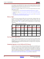
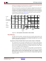
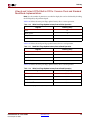
Memory Types
The FIFO Generator implements FIFOs built from block RAM, distributed RAM, shift
registers, or the built-in FIFOs for Virtex-6, Virtex-5 and Virtex-4 FPGAs. The core
combines memory primitives in an optimal configuration based on the selected width and
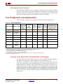
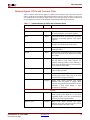
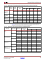
depth of the FIFO. Table 2-1 provides best-use recommendations for specific design
requirements.
Table 2-1:
Memory Configuration Benefits
Independent Common
Small
Clocks
Clock
Buffering
MediumLarge
Buffering
High
Minimal
Performance Resources
Built-in
FIFO
9
9
9
9
9
block RAM
9
9
9
9
9
9
9
9
9
9
9
Shift
Register
Distributed
RAM
9
Non-Symmetric Aspect Ratio
The core supports generating FIFOs whose write and read ports have different widths,
enabling automatic width conversion of the data width. Non-symmetric aspect ratios
ranging from 1:8 to 8:1 are supported for the write and read port widths. This feature is
available for FIFOs implemented with block RAM that are configured to have independent
write and read clocks.
Embedded Registers in block RAM and FIFO Macros
In Virtex-6, Virtex-5 and Virtex-4 FPGA block RAM and FIFO macros, embedded output
registers are available to increase performance and add a pipeline register to the macros.
This feature can be leveraged to add one additional latency to the FIFO core (DOUT bus
and VALID outputs) or implement the output registers for FWFT FIFOs. The embedded
registers available in Virtex-6 FPGAs can be reset (DOUT) to a default or user programmed
value for common clock built-in FIFOs. See “Embedded Registers in block RAM and FIFO
Macros (Virtex-6, Virtex-5 and Virtex-4 FPGAs),” page 70 for more information.
18
www.xilinx.com
FIFO Generator v5.1 User Guide
UG175 April 24, 2009
R
Core Configuration and Implementation
Error Injection and Correction
The block RAM and FIFO macros are equipped with built-in Error Correction Checking
(ECC) in the Virtex-5 FPGA architecture and built-in Error Injection and Correction Checking in the Virtex-6 FPGA architecture. Error Injection and Correction are available for both
the common and independent clock block RAM or built-in based FIFOs.
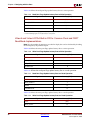
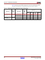
Core Configuration and Implementation
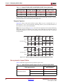
Table 2-2 provides a summary of the supported memory and clock configurations.
Table 2-2:
FIFO Configurations
Reset Option for
NonFirst-Word
Embedded
ECC
Error Embedded Register
symmetric
FallRegister
Clock Domain Memory Type
Injection (with/without DOUT
Aspect
Support
Through
Support
Reset Value)1
Ratios
1.
2.
3.
4.
5.
6.
7.
Common
Block RAM
Common
Distributed
RAM
Common
Shift Register
Common
Built-in FIFO3
Independent
Block RAM
Independent
Distributed
RAM
Independent
Built-in
FIFO3,6
9
9
9
9
92
9
9
94
9
9
9
9
95
9
9
92
9
94
9
97
Available only if Embedded register option is selected.
Embedded register support is only available for Virtex-4 and Virtex-5 FPGA block RAM-based FIFOs.
The built-in FIFO primitive is only available in the Virtex-5 and Virtex-4 architectures.
FWFT is only supported for built-in FIFOs in Virtex-5 devices.
Only available for Virtex-5 FPGA common clock built-in FIFOs.
For non-symmetric aspect ratios, use the block RAM implementation (feature not supported in built-in FIFO primitive).
Available only if ECC option is selected.
Common Clock: Block RAM, Distributed RAM, Shift Register
This implementation category allows the user to select block RAM, distributed RAM, or
shift register and supports a common clock for write and read data accesses.
The feature set supported for this configuration includes status flags (full, almost full,
empty, and almost empty) and programmable empty and full flags generated with userdefined thresholds. In addition, optional handshaking and error flags are supported (write
acknowledge, overflow, valid, and underflow), and an optional data count provides the
number of words in the FIFO. In addition, for the block RAM and distributed RAM
implementations, the user has the option to select a synchronous or asynchronous reset for
the core. For Virtex-6 and Virtex-5 FPGA designs, the block RAM FIFO configuration also
supports ECC.
FIFO Generator v5.1 User Guide
UG175 April 24, 2009
www.xilinx.com
19
R
Chapter 2: Core Overview
Common Clock: Virtex-6, VIrtex-5 or Virtex-4 FPGA Built-in FIFO
This implementation category allows the user to select the built-in FIFO available in the
Virtex-6, Virtex-5 or Virtex-4 FPGA architectures and supports a common clock for write
and read data accesses.
The feature set supported for this configuration includes status flags (full and empty) and
optional programmable full and empty flags with user-defined thresholds. In addition,
optional handshaking and error flags are available (write acknowledge, overflow, valid,
and underflow). The Virtex-6 and Virtex-5 FPGA built-in FIFO configurations also support
the built-in ECC feature.
Independent Clocks: Block RAM and Distributed RAM
This implementation category allows the user to select block RAM or distributed RAM and
supports independent clock domains for write and read data accesses. Operations in the
read domain are synchronous to the read clock and operations in the write domain are
synchronous to the write clock.
The feature set supported for this type of FIFO includes non-symmetric aspect ratios
(different write and read port widths), status flags (full, almost full, empty, and almost
empty), as well as programmable full and empty flags generated with user-defined
thresholds. Optional read data count and write data count indicators provide the number
of words in the FIFO relative to their respective clock domains. In addition, optional
handshaking and error flags are available (write acknowledge, overflow, valid, and
underflow). For Virtex-6 and Virtex-5 FPGA designs, the block RAM FIFO configuration
also supports ECC.
Independent Clocks: Built-in FIFO for Virtex-6, Virtex-5 or Virtex-4 FPGAs
This implementation category allows the user to select the built-in FIFO available in the
Virtex-6, Virtex-5 or Virtex-4 FPGA architectures. Operations in the read domain are
synchronous to the read clock and operations in the write domain are synchronous to the
write clock.
The feature set supported for this configuration includes status flags (full and empty) and
programmable full and empty flags generated with user-defined thresholds. In addition,
optional handshaking and error flags are available (write acknowledge, overflow, valid,
and underflow). The Virtex-6 and Virtex-5 FPGA built-in FIFO configurations also support
the built-in ECC feature.
20
www.xilinx.com
FIFO Generator v5.1 User Guide
UG175 April 24, 2009
R
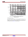
FIFO Generator Features
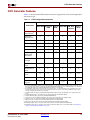
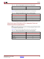
FIFO Generator Features
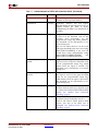
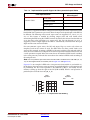
Table 2-3 summarizes the FIFO Generator features supported for each clock configuration
and memory type.
Table 2-3:
FIFO Configurations Summary
Independent Clocks
FIFO Feature
Block RAM
Non-symmetric
Aspect Ratios2
Symmetric
Aspect Ratios
Almost Full
Almost Empty
Handshaking
Data Count
Programmable
Empty/Full
Thresholds
First-Word FallThrough
Distributed
RAM
Common Clock
Built-in
Block RAM
FIFO1
Built-in
FIFO1
9
9
9
9
9
9
9
9
9
9
9
9
9
9
9
9
9
9
9
9
9
9
9
9
9
9
93
9
9
9
9
9
93
94
9
95
94
9
96
97
97
9
9
9
98
Synchronous
Reset
97
97
DOUT Reset
Value
9
9
ECC
99
Embedded
Register
910
Asynchronous
Reset
DistributedR
AM, Shift
Register
9
99
99
99
910
911
1. For Virtex-4 FPGA Built-in FIFO macro, the valid width range is 4, 9, 18 and 36 and the valid depth range automatically varies
based on write width selection. For Virtex-6 and Virtex-5 FPGA Built-in FIFO macros, the valid width range is 1 to 1024 and
the valid depth range is 512 to 4194304. Only depths with powers of 2 are allowed.
2. For applications with a single clock that require non-symmetric ports, use the independent clock configuration and connect
the write and read clocks to the same source. A dedicated solution for common clocks will be available in a future release.
Contact your Xilinx representative for more details.
3. For built-in FIFOs, the range of Programmable Empty/Full threshold is limited to take advantage of the logic internal to the
macro.
4. First-Word-Fall-Through is only supported for the Virtex-6 and Virtex-5 FPGA built-in FIFOs.
5. First-Word-Fall-Through is supported for distributed RAM FIFO only.
6. Synchronous reset is available and optional for all common clock configurations except built-in FIFO.
7. Asynchronous reset is optional for all FIFOs built using distributed and block RAM.
8. DOUT reset value is supported only in Virtex-6 FPGA common clock built-in FIFOs.
9. ECC is only supported for the Virtex-6 and Virtex-5 FPGAs and block RAM and built-in FIFOs.
10. Embedded register option is only supported in Virtex-6, VIrtex-5 and Virtex-4 FPGA block RAM FIFOs.
11. Embedded register option is supported only in Virtex-6 and VIrtex-5 FPGA common clock built-in FIFOs. See “Embedded
Registers in block RAM and FIFO Macros,” page 18.
FIFO Generator v5.1 User Guide
UG175 April 24, 2009
www.xilinx.com
21
R
Chapter 2: Core Overview
Using Block RAM FIFOs Instead of Built-in FIFOs
The Built-In FIFO solutions were implemented to take advantage of logic internal to the
Built-in FIFO macro. Several features, for example, non-symmetric aspect ratios, almost
full, almost empty, and so forth were not implemented because they are not native to the
macro and require additional logic in the fabric to implement.
Benchmarking suggests that the advantages the Built-In FIFO implementations have over
the block RAM FIFOs (for example, logic resources) diminish as external logic is added to
implement features not native to the macro. This is especially true as the depth of the
implemented FIFO increases. It is strongly recommended that users requiring features not
available in the Built-In FIFOs implement their design using block RAM FIFOs.
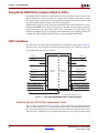
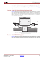
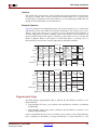
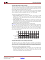
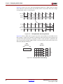
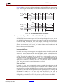
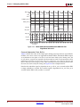
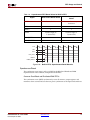
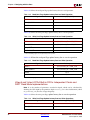
FIFO Interfaces
The following two sections provide definitions for the FIFO interface signals. Figure 2-1
illustrates these signals (both the standard and optional ports) for a FIFO core that supports independent write and read clocks.
DIN[N:0]
DOUT[M:0]
WR_EN
RD_EN
WR_CLK
RD_CLK
FULL
EMPTY
ALMOST_FULL
PROG_FULL
Write Clock
Domain
Read Clock
Domain
ALMOST_EMPTY
PROG_EMPTY
WR_ACK
VALID
OVERFLOW
UNDERFLOW
PROG_FULL_THRESH_ASSERT
PROG_EMPTY_THRESH_ASSERT
PROG_FULL_THRESH_NEGATE
PROG_EMPTY_THRESH_NEGATE
PROG_FULL_THRESH
PROG_EMPTY_THRESH
WR_RST
RD_RST
RST
Note: Optional ports represented in italics
Figure 2-1:
FIFO with Independent Clocks: Interface Signals
Interface Signals: FIFOs With Independent Clocks
The RST signal, as defined in Table 2-4, causes a reset of the entire core logic (both write
and read clock domains). It is an asynchronous input which is synchronized internally in
the core before being used. The initial hardware reset should be generated by the user.
When the core is configured to have independent clocks, the reset signal should be High
22
www.xilinx.com
FIFO Generator v5.1 User Guide
UG175 April 24, 2009
R
FIFO Interfaces
for at least three read clock and write clock cycles to ensure all internal states are reset to
the correct values.
Table 2-4:
Reset Signal for FIFOs with Independent Clocks
Name
RST
Direction
Description
Input
Reset: An asynchronous reset signal that
initializes all internal pointers, output
registers and memory1.
1. Output of FIFO (DOUT) is reset and not the content of the memory.
Table 2-5 defines the signals for the write interface for FIFOs with independent clocks. The
write interface signals are divided into required and optional signals and all signals are
synchronous to the write clock (WR_CLK).
Table 2-5:
Write Interface Signals for FIFOs with Independent Clocks
Name
Direction
Description
Required
WR_CLK
Input
Write Clock: All signals on the write domain are
synchronous to this clock.
DIN[N:0]
Input
Data Input: The input data bus used when
writing the FIFO.
WR_EN
Input
Write Enable: If the FIFO is not full, asserting this
signal causes data (on DIN) to be written to the
FIFO.
Output
Full Flag: When asserted, this signal indicates
that the FIFO is full. Write requests are ignored
when the FIFO is full, initiating a write when the
FIFO is full is non-destructive to the contents of
the FIFO.
FULL
Optional
WR_RST
Input
Write Reset: Synchronous to write clock. When
asserted, initializes all internal pointers and flags
of write clock domain.
ALMOST_FULL
Output
Almost Full: When asserted, this signal indicates
that only one more write can be performed before
the FIFO is full.
PROG_FULL
Output
Programmable Full: This signal is asserted when
the number of words in the FIFO is greater than
or equal to the assert threshold. It is deasserted
when the number of words in the FIFO is less
than the negate threshold.
FIFO Generator v5.1 User Guide
UG175 April 24, 2009
www.xilinx.com
23
R
Chapter 2: Core Overview
Table 2-5:
Write Interface Signals for FIFOs with Independent Clocks (Continued)
Name
WR_DATA_COUNT [D:0]
Direction
Description
Output
Write Data Count: This bus indicates the number
of words written into in the FIFO. The count is
guaranteed to never under-report the number of
words in the FIFO, to ensure the user never
overflows the FIFO. The exception to this
behavior is when a write operation occurs at the
rising edge of WR_CLK, that write operation will
only be reflected on WR_DATA_COUNT at the
next rising clock edge.
If D is less than log2(FIFO depth)-1, the bus is
truncated by removing the least-significant bits.
WR_ACK
Output
Write Acknowledge: This signal indicates that a
write request (WR_EN) during the prior clock
cycle succeeded.
OVERFLOW
Output
Overflow: This signal indicates that a write
request (WR_EN) during the prior clock cycle
was rejected, because the FIFO is full.
Overflowing the FIFO is non-destructive to the
contents of the FIFO.
Input
Programmable Full Threshold: This signal is used
to input the threshold value for the assertion and
deassertion
of
the
programmable
full
(PROG_FULL) flag. The threshold can be
dynamically set in-circuit during reset.
PROG_FULL_THRESH
The user can either choose to set the assert and
negate threshold to the same value (using
PROG_FULL_THRESH), or the user can control
these
values
independently
(using
PROG_FULL_THRESH_ASSERT
and
PROG_FULL_THRESH_NEGATE).
24
PROG_FULL_THRESH_
ASSERT
Input
Programmable Full Threshold Assert: This signal
is used to set the upper threshold value for the
programmable full flag, which defines when the
signal is asserted. The threshold can be
dynamically set in-circuit during reset.
PROG_FULL_THRESH_
NEGATE
Input
Programmable Full Threshold Negate: This
signal is used to set the lower threshold value for
the programmable full flag, which defines when
the signal is deasserted. The threshold can be
dynamically set in-circuit during reset.
www.xilinx.com
FIFO Generator v5.1 User Guide
UG175 April 24, 2009
R
FIFO Interfaces
Table 2-5:
Write Interface Signals for FIFOs with Independent Clocks (Continued)
Name
INJECTSBITERR
INJECTDBITERR
Direction
Description
Input
Injects a single bit error if the ECC feature is
used on a Virtex-6 FPGA block RAM or
built-in FIFO macro. For detailed
information, see "Chapter 4, Designing with
the Core," in the FIFO Generator User Guide.
Input
Injects a double bit error the ECC feature is
used on a Virtex-6 FPGA block RAM or
built-in FIFO macro. For detailed
information, see "Chapter 4, Designing with
the Core," in the FIFO Generator User Guide.
Table 2-6 defines the signals on the read interface of a FIFO with independent clocks. The
read interface signals are divided into required signals and optional signals, and all signals
are synchronous to the read clock (RD_CLK).
Table 2-6:
Read Interface Signals for FIFOs with Independent Clocks
Name
Direction
Description
Required
Input
Read Clock: All signals on the read domain are
synchronous to this clock.
Output
Data Output: The output data bus is driven when
reading the FIFO.
RD_EN
Input
Read Enable: If the FIFO is not empty, asserting this
signal causes data to be read from the FIFO (output
on DOUT).
EMPTY
Output
Empty Flag: When asserted, this signal indicates that
the FIFO is empty. Read requests are ignored when
the FIFO is empty, initiating a read while empty is
non-destructive to the FIFO.
RD_CLK
DOUT[M:0]
Optional
RD_RST
Input
Read Reset: Synchronous to read clock. When
asserted, initializes all internal pointers, flags and
output registers of read clock domain.
ALMOST_EMPTY
Output
Almost Empty Flag: When asserted, this signal
indicates that the FIFO is almost empty and one
word remains in the FIFO.
PROG_EMPTY
Output
Programmable Empty: This signal is asserted when
the number of words in the FIFO is less than or equal
to the programmable threshold. It is deasserted
when the number of words in the FIFO exceeds the
programmable threshold.
FIFO Generator v5.1 User Guide
UG175 April 24, 2009
www.xilinx.com
25
R
Chapter 2: Core Overview
Table 2-6:
Read Interface Signals for FIFOs with Independent Clocks (Continued)
Name
RD_DATA_COUNT [C:0]
Direction
Description
Output
Read Data Count: This bus indicates the number of
words available for reading in the FIFO. The count is
guaranteed to never over-report the number of
words available for reading, to ensure that the user
does not underflow the FIFO. The exception to this
behavior is when the read operation occurs at the
rising edge of RD_CLK, that read operation will only
be reflected on RD_DATA_COUNT at the next rising
clock edge.
If C is less than log2(FIFO depth)-1, the bus is
truncated by removing the least-significant bits.
VALID
Output
Valid: This signal indicates that valid data is
available on the output bus (DOUT).
UNDERFLOW
Output
Underflow: Indicates that the read request (RD_EN)
during the previous clock cycle was rejected because
the FIFO is empty. Underflowing the FIFO is not
destructive to the FIFO.
Input
Programmable Empty Threshold: This signal is used
to input the threshold value for the assertion and
deassertion
of
the
programmable
empty
(PROG_EMPTY) flag. The threshold can be
dynamically set in-circuit during reset.
PROG_EMPTY_THRESH
The user can either choose to set the assert and
negate threshold to the same value (using
PROG_EMPTY_THRESH), or the user can control
these
values
independently
(using
PROG_EMPTY_THRESH_ASSERT
and
PROG_EMPTY_THRESH_NEGATE).
26
PROG_EMPTY_THRESH_
ASSERT
Input
Programmable Empty Threshold Assert: This signal
is used to set the lower threshold value for the
programmable empty flag, which defines when the
signal is asserted. The threshold can be dynamically
set in-circuit during reset.
PROG_EMPTY_THRESH_
NEGATE
Input
Programmable Empty Threshold Negate: This signal
is used to set the upper threshold value for the
programmable empty flag, which defines when the
signal is deasserted. The threshold can be
dynamically set in-circuit during reset.
SBITERR
Output
Single Bit Error: Indicates that the ECC decoder
detected and fixed a single-bit error on a Virtex-6 and
Virtex-5 FPGA block RAMs or built-in FIFO macros.
See “Built-in Error Correction Checking,” page 71.
DBITERR
Output
Double Bit Error: Indicates that the ECC decoder
detected a double-bit error on a Virtex-6 and
Virtex-5 FPGA block RAMs or built-in FIFO macros
and data in the FIFO core is corrupted. See “Built-in
Error Correction Checking,” page 71.
www.xilinx.com
FIFO Generator v5.1 User Guide
UG175 April 24, 2009
R
FIFO Interfaces
Interface Signals: FIFOs with Common Clock
Table 2-7 defines the interface signals of a FIFO with a common write and read clock. The
table is divided into standard and optional interface signals, and all signals (except reset)
are synchronous to the common clock (CLK). Users have the option to select synchronous
or asynchronous reset for the distributed or block RAM FIFO implementation.
Table 2-7:
Interface Signals for FIFOs with a Common Clock
Name
Direction
Description
Required
RST
Input
Reset: An asynchronous reset that initializes
all internal pointers and output registers.
SRST
Input
Synchronous Reset: A synchronous reset that
initializes all internal pointers and output
registers.
CLK
Input
Clock: All signals on the write and read
domains are synchronous to this clock.
DIN[N:0]
Input
Data Input: The input data bus used when
writing the FIFO.
WR_EN
Input
Write Enable: If the FIFO is not full, asserting
this signal causes data (on DIN) to be written
to the FIFO.
FULL
Output
Full Flag: When asserted, this signal indicates
that the FIFO is full. Write requests are
ignored when the FIFO is full, initiating a
write when the FIFO is full is non-destructive
to the contents of the FIFO.
DOUT[M:0]
Output
Data Output: The output data bus driven
when reading the FIFO.
RD_EN
Input
Read Enable: If the FIFO is not empty,
asserting this signal causes data to be read
from the FIFO (output on DOUT).
EMPTY
Output
Empty Flag: When asserted, this signal
indicates that the FIFO is empty. Read
requests are ignored when the FIFO is empty,
initiating a read while empty is nondestructive to the FIFO.
Optional
DATA_COUNT [C:0]
Output
Data Count: This bus indicates the number of
words stored in the FIFO. If C is less than
log2(FIFO depth)-1, the bus is truncated by
removing the least-significant bits.
ALMOST_FULL
Output
Almost Full: When asserted, this signal
indicates that only one more write can be
performed before the FIFO is full.
FIFO Generator v5.1 User Guide
UG175 April 24, 2009
www.xilinx.com
27
R
Chapter 2: Core Overview
Table 2-7:
Interface Signals for FIFOs with a Common Clock (Continued)
Name
Direction
Description
PROG_FULL
Output
Programmable Full: This signal is asserted
when the number of words in the FIFO is
greater than or equal to the assert threshold. It
is deasserted when the number of words in
the FIFO is less than the negate threshold.
WR_ACK
Output
Write Acknowledge: This signal indicates
that a write request (WR_EN) during the
prior clock cycle succeeded.
OVERFLOW
Output
Overflow: This signal indicates that a write
request (WR_EN) during the prior clock cycle
was rejected, because the FIFO is full.
Overflowing the FIFO is non-destructive to
the contents of the FIFO.
Input
Programmable Full Threshold: This signal is
used to set the threshold value for the
assertion
and
deassertion
of
the
programmable full flag (PROG_FULL). The
threshold can be dynamically set in-circuit
during reset.
PROG_FULL_THRESH
The user can either choose to set the assert
and negate threshold to the same value (using
PROG_FULL_THRESH), or the user can
control these values independently (using
PROG_FULL_THRESH_ASSERT
and
PROG_FULL_THRESH_NEGATE).
28
PROG_FULL_THRESH_
ASSERT
Input
Programmable Full Threshold Assert: This
signal is used to set the upper threshold value
for the programmable full flag, which defines
when the signal is asserted. The threshold can
be dynamically set in-circuit during reset.
PROG_FULL_THRESH_
NEGATE
Input
Programmable Full Threshold Negate: This
signal is used to set the lower threshold value
for the programmable full flag, which defines
when the signal is deasserted. The threshold
can be dynamically set in-circuit during reset.
ALMOST_EMPTY
Output
Almost Empty Flag: When asserted, this
signal indicates that the FIFO is almost empty
and one word remains in the FIFO.
PROG_EMPTY
Output
Programmable Empty: This signal is asserted
after the number of words in the FIFO is less
than or equal to the programmable threshold.
It is deasserted when the number of words in
the FIFO exceeds the programmable
threshold.
www.xilinx.com
FIFO Generator v5.1 User Guide
UG175 April 24, 2009
R
FIFO Interfaces
Table 2-7:
Interface Signals for FIFOs with a Common Clock (Continued)
Name
Direction
Description
VALID
Output
Valid: This signal indicates that valid data is
available on the output bus (DOUT).
UNDERFLOW
Output
Underflow: Indicates that read request
(RD_EN) during the previous clock cycle was
rejected because the FIFO is empty.
Underflowing the FIFO is not destructive to
the FIFO.
Input
Programmable Empty Threshold: This signal
is used to set the threshold value for the
assertion
and
deassertion
of
the
programmable empty flag (PROG_EMPTY).
The threshold can be dynamically set incircuit during reset.
PROG_EMPTY_THRESH
The user can either choose to set the assert
and negate threshold to the same value (using
PROG_EMPTY_THRESH), or the user can
control these values independently (using
PROG_EMPTY_THRESH_ASSERT
and
PROG_EMPTY_THRESH_NEGATE).
PROG_EMPTY_THRESH_
ASSERT
Input
Programmable Empty Threshold Assert: This
signal is used to set the lower threshold value
for the programmable empty flag, which
defines when the signal is asserted. The
threshold can be dynamically set in-circuit
during reset.
PROG_EMPTY_THRESH_
NEGATE
Input
Programmable Empty Threshold Negate:
This signal is used to set the upper threshold
value for the programmable empty flag,
which defines when the signal is deasserted.
The threshold can be dynamically set incircuit during reset.
SBITERR
Output
Single Bit Error: Indicates that the ECC
decoder detected and fixed a single-bit error
on a Virtex-6 and Virtex-5 FPGA built-in FIFO
macros. See “Built-in Error Correction
Checking,” page 71.
DBITERR
Output
Double Bit Error: Indicates that the ECC
decoder detected a double-bit error on a
Virtex-6 and Virtex-5 FPGA built-in FIFO
macros, and data in the FIFO core is
corrupted. See “Built-in Error Correction
Checking,” page 71.
FIFO Generator v5.1 User Guide
UG175 April 24, 2009
www.xilinx.com
29
R
Chapter 2: Core Overview
Table 2-7:
Interface Signals for FIFOs with a Common Clock (Continued)
Name
INJECTSBITERR
INJECTDBITERR
30
Direction
Description
Input
Injects a single bit error if the ECC feature is
used on a Virtex-6 FPGA block RAM or builtin FIFO macro. For detailed information, see
"Chapter 4, Designing with the Core," in the
FIFO Generator User Guide.
Input
Injects a double bit error if the ECC feature is
used on a Virtex-6 FPGA block RAM or builtin FIFO macro. For detailed information, see
"Chapter 4, Designing with the Core," in the
FIFO Generator User Guide.
www.xilinx.com
FIFO Generator v5.1 User Guide
UG175 April 24, 2009
R
Chapter 3
Generating the Core
This chapter contains information and instructions for using the Xilinx CORE Generator
system to customize the FIFO Generator.
CORE Generator Graphical User Interface
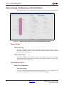
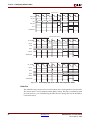
The FIFO Generator GUI includes six configuration screens.
•
FIFO Implementation
•
Performance Options and Data Port Parameters
•
Optional Flags, Handshaking, and Initialization
•
Initialization and Programmable Flags
•
Data Count
•
Summary
FIFO Generator v5.1 User Guide
UG175 April 24, 2009
www.xilinx.com
31
R
Chapter 3: Generating the Core
FIFO Implementation
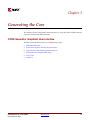
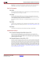
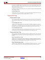
The main FIFO Generator screen is used to define the component name and provides
configuration options for the core.
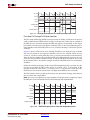
Figure 3-1:
Main FIFO Generator Screen
Component Name
Base name of the output files generated for this core. The name must begin with a letter
and be composed of the following characters: a to z, 0 to 9, and “_”.
FIFO Implementation
This section of the GUI allows the user to select from a set of available FIFO
implementations and supported features. The key supported features that are only
available for certain implementations are highlighted by checks in the right-margin. The
available options are listed below, with cross-references to additional information.
32
www.xilinx.com
FIFO Generator v5.1 User Guide
UG175 April 24, 2009
R
FIFO Implementation
Common Clock (CLK), Block RAM
For details, see “Common Clock FIFO: Block RAM and Distributed RAM,” page 49. This
implementation optionally supports first-word-fall-through (selectable in the second GUI
screen, shown in Figure 3-2).
Common Clock (CLK), Distributed RAM
For details, see “Common Clock FIFO: Block RAM and Distributed RAM,” page 49. This
implementation optionally supports first-word-fall-through (selectable in the second GUI
screen, shown in Figure 3-2).
Common Clock (CLK), Shift Register
For details, see “Common Clock FIFO: Shift Registers,” page 49. This implementation is
only available in Virtex-4 FPGA and newer architectures.
Common Clock (CLK), Built-in FIFO
For details, see “Common Clock: Built-in FIFO,” page 48. This implementation is only
available when using the Virtex-6, Virtex-5 or Virtex-4 FPGA architectures. This
implementation optionally supports first-word fall-through (selectable in the second GUI
screen, shown in Figure 3-2).
Independent Clocks (RD_CLK, WR_CLK), Block RAM
For details, see “Independent Clocks: Block RAM and Distributed RAM,” page 45. This
implementation optionally supports asymmetric read/write ports and first-word fallthrough (selectable in the second GUI screen, shown in Figure 3-2).
Independent Clocks (RD_CLK, WR_CLK), Distributed RAM
For more information, see “Independent Clocks: Block RAM and Distributed RAM,” page
45. This implementation optionally supports first-word fall-through (selectable in the
second GUI screen, shown in Figure 3-2).
Independent Clocks (RD_CLK, WR_CLK), Built-in FIFO
For more information, see “Independent Clocks: Built-in FIFO,” page 47. This
implementation is only available when using Virtex-6, Virtex-5 or Virtex-4 FPGA
architectures. This implementation optionally supports first-word fall-through (selectable
in the second GUI screen, shown in Figure 3-2).
FIFO Generator v5.1 User Guide
UG175 April 24, 2009
www.xilinx.com
33
R
Chapter 3: Generating the Core
Performance Options and Data Port Parameters
This screen provides performance options and data port parameters for the core.
Figure 3-2:
Performance Options and Data Port Parameters Screen
Read Mode
Available only when block RAM or distributed RAM FIFOs are selected. Support for builtin FIFOs is only available for Virtex-6 and Virtex-5 FPGA implementations.
Standard FIFO
Implements a FIFO with standard latencies, and without using output registers.
First-Word Fall-Through FIFO
Implements a FIFO with registered outputs. For more information about FWFT
functionality, see “First-Word-Fall-Through FIFO Read Operation,” page 53.
Built-in FIFO Options
Read/Write Clock Frequencies
The Read Clock Frequency and Write Clock Frequency fields can be any integer from 1 to
1000. They are used to determine the optimal implementation of the domain-crossing logic
in the core. This option is only available for built-in FIFOs with independent clocks. If the
desired frequency is not within the allowable range, scale the read and write clock
frequencies so that they fit within the valid range, while maintaining their ratio
relationship.
34
www.xilinx.com
FIFO Generator v5.1 User Guide
UG175 April 24, 2009
R
Performance Options and Data Port Parameters
Important: It is critical that this information is entered and accurate. If this information is
not provided, it can result in a sub-optimal solution with incorrect core behavior.
Data Port Parameters
Write Width
For Virtex-4 FPGA Built-in FIFO macro, the valid range is 4, 9, 18 and 36. For other memory
type configurations, the valid range is 1 to 1024.
Write Depth
For Virtex-4 FPGA Built-in FIFO macro, the valid range automatically varies based on
write width selection. For Virtex-6 and Virtex-5 FPGA Built-in FIFO macro, the valid range
is 512 to 4194304. Only depths with powers of 2 are allowed.
For non Built-in FIFO, the valid range is 1 to 4194304. Only depths with powers of 2 are
allowed.
Read Width
Available only if independent clocks configuration with block RAM is selected. Valid
range must comply with asymmetric port rules. See “Non-symmetric Aspect Ratios,” page
66.
Read Depth
Automatically calculated based on Write Width, Write Depth, and Read Width.
Implementation Options
Error Correction Checking in Block RAM or Built-in FIFO
The Error Correction Checking (ECC) feature enables built-in error correction in the
Virtex-6 and Virtex-5 FPGA block RAM and built-in FIFO macros. When this feature is
enabled, the block RAM or built-in FIFO is set to the full ECC mode, where both the
encoder and decoder are enabled.
Use Embedded Registers in Block RAM or FIFO
For Virtex-6, Virtex-5 and Virtex-6 FPGA architectures, the built-in FIFO and block RAM
macros have built-in embedded registers that can be used to pipeline data and improve
macro timing. This option enables users to add one pipeline stage to the output of the FIFO
and take advantage of the available embedded registers; however, the ability to reset the
data output of the FIFO is disabled when this feature is used. For built-in FIFOs, this
feature is only supported for synchronous FIFO configurations that have only 1 FIFO
macro in depth. See “Embedded Registers in block RAM and FIFO Macros (Virtex-6,
Virtex-5 and Virtex-4 FPGAs),” page 70.
FIFO Generator v5.1 User Guide
UG175 April 24, 2009
www.xilinx.com
35
R
Chapter 3: Generating the Core
Optional Flags, Handshaking, and Initialization
This screen allows you to select the optional status flags and set the handshaking options.
Figure 3-3:
Optional Flags, Handshaking, and Initialization Options Screen
Optional Flags
Almost Full Flag
Available in all FIFO implementations except those using Virtex-6, Virtex-5 or Virtex-4
FPGA built-in FIFOs. Generates an output port that indicates the FIFO is almost full (only
one more word can be written).
Almost Empty Flag
Available in all FIFO implementations except in those using Virtex-6, Virtex-5 or Virtex-4
FPGA built-in FIFOs. Generates an output port that indicates the FIFO is almost empty
(only one more word can be read).
Handshaking Options
Write Port Handshaking
Write Acknowledge
Generates write acknowledge flag which reports the success of a write operation. This
signal can be configured to be active high or low (default active high).
36
www.xilinx.com
FIFO Generator v5.1 User Guide
UG175 April 24, 2009
R
Optional Flags, Handshaking, and Initialization
Overflow (Write Error)
Generates overflow flag which indicates when the previous write operation was not
successful. This signal can be configured to be active high or low (default active high).
Read Port Handshaking
Valid (Read Acknowledge)
Generates valid flag which indicates when the data on the output bus is valid. This signal
can be configured to be active high or low (default active high).
Underflow (Read Error)
Generates underflow flag to indicate that the previous read request was not successful.
This signal can be configured to be active high or low (default active high).
Error Injection
Single Bit Error Injection
Available only in Virtex-6 FPGAs for both the common and independent clock block RAM
or built-in FIFOs, with ECC option enabled. Generates an input port to inject a single bit
error on write and an output port that indicates a single bit error occurred.
Double Bit Error Injection
Available only in Virtex-6 FPGAs for both the common and independent clock block RAM
or built-in FIFOs, with ECC option enabled. Generates an input port to inject a double bit
error on write and an output port that indicates a double bit error occurred.
FIFO Generator v5.1 User Guide
UG175 April 24, 2009
www.xilinx.com
37
R
Chapter 3: Generating the Core
Initialization and Programmable Flags
Use this screen to select the initialization values and programmable flag type when
generating a specific FIFO Generator configuration.
Figure 3-4: Programmable Flags Screen
Initialization
Reset Pin
For FIFOs implemented with block RAM or distributed RAM, a reset pin is not required,
and the input pin is optional.
•
Enable Reset Synchronization. Optional selection only available for independent clock
block RAM or distributed RAM FIFOs. When unchecked, WR_RST/RD_RST is
available. See “Reset Behavior” in Chapter 4 for details.
•
Asynchronous Reset. Optional selection for a common-clock FIFO implemented using
distributed or block RAM.
•
Synchronous Reset. Optional selection for a a common-clock FIFO implemented using
distributed or block RAM.
Full Flags Reset Value
For block RAM, distributed RAM, and shift register configurations, the user can choose the
reset value of the full flags (PROG_FULL, ALMOST_FULL, and FULL) during asynchronous
reset.
Use Dout Reset
Available in Virtex-4 FPGA or newer architectures for all implementations using block
RAM, distributed RAM, or shift register. Only available if a reset pin (RST or SRST) is used.
38
www.xilinx.com
FIFO Generator v5.1 User Guide
UG175 April 24, 2009
R
Initialization and Programmable Flags
If selected, the DOUT output of the FIFO will reset to the defined DOUT Reset Value
(below) when the reset is asserted. If not selected, the DOUT output of the FIFO will not be
effected by the assertion of reset.
Disabling this feature for Spartan®-3 devices may improve timing for the distributed RAM
and shift register FIFO.
Use Dout Reset Value
Available only when Use Dout Reset is selected, this field indicates the hexidecimal value
asserted on the output of the FIFO when RST (SRST) is asserted.
Programmable Flags
Programmable Full Type
Select a programmable full threshold type from the drop-down menu. The valid range for
each threshold is displayed and varies depending on the options selected elsewhere in the
GUI.
Full Threshold Assert Value
Available when Programmable Full with Single or Multiple Threshold Constants is
selected. Enter a user-defined value. The valid range for this threshold is provided in the
GUI. When using a single threshold constant, only the assert threshold value is used.
Full Threshold Negate Value
Available when Programmable Full with Multiple Threshold Constants is selected. Enter a
user-defined value. The valid range for this threshold is provided in the GUI.
Programmable Empty Type
Select a programmable empty threshold type from the drop-down menu. The valid range
for each threshold is displayed, and will vary depending on options selected elsewhere in
the GUI.
Empty Threshold Assert Value
Available when Programmable Empty with Single or Multiple Threshold Constants is
selected. Enter a user-defined value. The valid range for this threshold is provided in the
GUI. When using a single threshold constant, only the assert value is used.
Empty Threshold Negate Value
Available when Programmable Empty with Multiple Threshold Constants is selected.
Enter a user-defined value. The valid range for this threshold is provided in the GUI.
FIFO Generator v5.1 User Guide
UG175 April 24, 2009
www.xilinx.com
39
R
Chapter 3: Generating the Core
Data Count
Use this screen to set data count options.
Figure 3-5:
Data Count and Reset Screen
Data Count Options
Use Extra Logic For More Accurate Data Counts
Only available for independent clocks FIFO with block RAM or distributed RAM, and
when using first-word fall-through. This option uses additional external logic to generate
a more accurate data count. This feature is always enabled for common clock FIFOs with
block RAM or distributed RAM and when using first-word-fall-through. See “First-Word
Fall-Through Data Count,” page 64 for details.
Data Count (Synchronized With Clk)
Available when a common clock FIFO with block RAM, distributed RAM, or shift registers
is selected.
Data Count Width
Available when Data Count is selected. Valid range is from 1 to log2 (input depth).
Write Data Count (Synchronized with Write Clk)
Available when an independent clocks FIFO with block RAM or distributed RAM is
selected.
40
www.xilinx.com
FIFO Generator v5.1 User Guide
UG175 April 24, 2009
R
Summary
Write Data Count Width
Available when Write Data Count is selected. Valid range is from 1 to log2 (input depth).
Read Data Count (Synchronized with Read Clk)
Available when an independent clocks FIFO with block RAM or distributed RAM is
selected.
Read Data Count Width
Available when Read Data Count is selected. Valid range is from 1 to log2 (output depth).
Summary
This screen displays a summary of the selected FIFO options, including the FIFO type,
FIFO dimensions, and the status of any additional features selected. In the Additional
Features section, most features display either Not Selected (if unused), or Selected (if used).
Note: Write depth and read depth provide the actual FIFO depths for the selected configuration.
These depths may differ slightly from the depth selected on screen 2 of the FIFO GUI.
Figure 3-6:
FIFO Generator v5.1 User Guide
UG175 April 24, 2009
Summary Screen
www.xilinx.com
41
R
Chapter 3: Generating the Core
42
www.xilinx.com
FIFO Generator v5.1 User Guide
UG175 April 24, 2009
R
Chapter 4
Designing with the Core
This chapter describes the steps required to turn a FIFO Generator core into a fully
functioning design integrated with the user application logic. It is important to note that
depending on the configuration of the FIFO core, only a subset of the implementation
details provided are applicable. For successful use of a FIFO core, the design guidelines
discussed in this chapter must be observed.
General Design Guidelines
Know the Degree of Difficulty
A fully-compliant and feature-rich FIFO design is challenging to implement in any
technology. For this reason, it is important to understand that the degree of difficulty can
be significantly influenced by
•
Maximum system clock frequency
•
Targeted device architecture
•
Specific user application
Ensure that design techniques are used to facilitate implementation, including pipelining
and use of constraints (timing constraints, and placement and/or area constraints).
Understand Signal Pipelining and Synchronization
To understand the nature of FIFO designs, it is important to understand how pipelining is
used to maximize performance and implement synchronization logic for clock-domain
crossing. Data written into the write interface may take multiple clock cycles before it can
be accessed on the read interface.
Synchronization Considerations
FIFOs with independent write and read clocks require that interface signals be used only in
their respective clock domains. The independent clocks FIFO handles all synchronization
requirements, enabling the user to cross between two clock domains that have no
relationship in frequency or phase.
Important: FIFO Full and Empty flags must be used to guarantee proper behavior.
Figure 4-1 shows the signals with respect to their clock domains. All signals are
synchronous to a specific clock, with the exception of RST, which performs an
asynchronous reset of the entire FIFO.
FIFO Generator v5.1 User Guide
UG175 April 24, 2009
www.xilinx.com
43
R
Chapter 4: Designing with the Core
.
DIN[N:0]
DOUT[M:0]
WR_EN
RD_EN
WR_CLK
RD_CLK
FULL
EMPTY
ALMOST_FULL
Write Clock
Domain
PROG_FULL
WR_ACK
Read Clock
Domain
ALMOST_EMPTY
PROG_EMPTY
VALID
OVERFLOW
UNDERFLOW
PROG_FULL_THRESH_ASSERT
PROG_EMPTY_THRESH_ASSERT
PROG_FULL_THRESH_NEGATE
PROG_EMPTY_THRESH_NEGATE
PROG_FULL_THRESH
PROG_EMPTY_THRESH
WR_RST
RD_RST
RST
Note: Optional ports represented in italics
Figure 4-1: FIFO with Independent Clocks: Write and Read Clock Domains
For write operations, the write enable signal (WR_EN) and data input (DIN) are
synchronous to WR_CLK. For read operations, the read enable (RD_EN) and data output
(DOUT) are synchronous to RD_CLK. All status outputs are synchronous to their respective
clock domains and can only be used in that clock domain. The performance of the FIFO can
be measured by independently constraining the clock period for the WR_CLK and RD_CLK
input signals.
The interface signals are evaluated on their rising clock edge (WR_CLK and RD_CLK). They
can be made falling-edge active (relative to the clock source) by inserting an inverter
between the clock source and the FIFO clock inputs. This inverter is absorbed into the
internal FIFO control logic and does not cause a decrease in performance or increase in
logic utilization.
Initializing the FIFO Generator
When designing with the built-in FIFO or common clock shift register FIFO, the FIFO must
be reset after the FPGA is configured and before operation begins. An asynchronous reset
pin (RST) is provided, which is an asynchronous reset that clears the internal counters and
output registers.
For FIFOs implemented with block RAM or distributed RAM, a reset is not required, and
the input pin is optional. For common clock configurations, users have the option of
asynchronous or synchronous reset. For independent clock configurations, users have the
option of asynchronous reset (RST) or synchronous reset (WR_RST/RD_RST) with respect
to respective clock domains.
When asynchronous reset is implemented (Enable Reset Synchronization option is
selected), it is synchronized to the clock domain in which it is used to ensure that the FIFO
initializes to a known state. This synchronization logic allows for proper reset timing of the
core logic, avoiding glitches and metastable behavior. The reset pulse and synchronization
delay requirements are dependent on the FIFO implementation types.
44
www.xilinx.com
FIFO Generator v5.1 User Guide
UG175 April 24, 2009
R
FIFO Implementations
When WR_RST/RD_RST is implemented (Enable Reset Synchronization option is not
selected), the WR_RST/RD_RST is treated as a synchronous reset to the respective clock
domain. The write clock domain remains in reset state as long as WR_RST is asserted, and
the read clock domain remains in reset state as long as RD_RST is asserted. See “Reset
Behavior,” page 73.
FIFO Implementations
Each FIFO configuration has a set of allowable features, as defined in Table 2-3, page 21.
Independent Clocks: Block RAM and Distributed RAM
Figure 4-2 illustrates the functional implementation of a FIFO configured with
independent clocks. This implementation uses block RAM or distributed RAM for
FIFO Generator v5.1 User Guide
UG175 April 24, 2009
www.xilinx.com
45
R
Chapter 4: Designing with the Core
memory, counters for write and read pointers, conversions between binary and Gray code
for synchronization across clock domains, and logic for calculating the status flags.
Figure Top x-ref 1
WRITE CLOCK DOMAIN
READ CLOCK DOMAIN
EMPTY
ALMOST_EMPTY
Read Flag
Logic
PROG_EMPTY
RD_DATA_COUNT
Read Counter
Binary to Gray
Converter
Gray to Binary
Converter
MEMORY
WRITE PORT
Write Counter
ADDRA
WR_EN
READ PORT
DOUT
OPTIONAL:
First Word Fall
Through Logic
WE
ADDRB
DIN
Read Counter
DOUT
RD_EN
DIN
Gray to Binary
Converters
Binary to Gray
Converters
Write Counter
FULL
ALMOST_FULL
PROG_FULL
Write Flag
Logic
WR_DATA_COUNT
Figure 4-2:
46
Functional Implementation of a FIFO with Independent Clock Domains
www.xilinx.com
FIFO Generator v5.1 User Guide
UG175 April 24, 2009
R
FIFO Implementations
This FIFO is designed to support an independent read clock (RD_CLK) and write clock
(WR_CLK); in other words, there is no required relationship between RD_CLK and WR_CLK
with regard to frequency or phase. Table 4-1 summarizes the FIFO interface signals, which
are only valid in their respective clock domains.
Table 4-1:
Interface Signals and Corresponding Clock Domains
WR_CLK
RD_CLK
DIN
DOUT
WR_EN
RD_EN
FULL
EMPTY
ALMOST_FULL
ALMOST_EMPTY
PROG_FULL
PROG_EMPTY
WR_ACK
VALID
OVERFLOW
UNDERFLOW
WR_DATA_COUNT
RD_DATA_COUNT
WR_RST
SBITERR
INJECTSBITERR
DBITERR
INJECTDBITERR
RD_RST
For FIFO cores using independent clocks, the timing relationship between the write and
read operations and the status flags is affected by the relationship of the two clocks. For
example, the timing between writing to an empty FIFO and the deassertion of EMPTY is
determined by the phase and frequency relationship between the write and read clocks.
For additional information refer to the “Synchronization Considerations,” page 43.
Independent Clocks: Built-in FIFO
Figure 4-3 illustrates the functional implementation of FIFO configured with independent
clocks using the Virtex-6 and Virtex-5 FPGA built-in FIFO primitive. This design
implementation consists of cascaded built-in FIFO primitives and handshaking logic. The
number of built-in primitives depends on the FIFO width and depth requested.
The Virtex-4 FPGA built-in FIFO implementation allows generation of a single primitive. The
generated core includes a FIFO flag patch (defined in "Solution 1: Synchronous/Asynchronous
Clock Work-Arounds," in the Virtex-4 FPGA User Guide).
FIFO Generator v5.1 User Guide
UG175 April 24, 2009
www.xilinx.com
47
R
Chapter 4: Designing with the Core
WRITE DOMAIN
READ DOMAIN
Cascaded Built-in FIFO Primitives
PROG_FULL
PROG_EMPTY
FULL
EMPTY
WR_EN
WE
DIN
DIN
WR_ACK
Built-In
FIFO
Logic For
Optional Flags:
Write Domain
OVERFLOW
Figure 4-3:
RD_EN
RE
DOUT
DOUT
Logic For
Optional Flags:
Read Domain
UNDERFLOW
VALID
Functional Implementation of Built-in FIFO
This FIFO is designed to support an independent read clock (RD_CLK) and write clock
(WR_CLK); in other words, there is no required relationship between RD_CLK and WR_CLK
with regard to frequency or phase. Table 4-2 summarizes the FIFO interface signals, which
are only valid in their respective clock domains.
Table 4-2:
Interface Signals and Corresponding Clock Domains
WR_CLK
RD_CLK
DIN
DOUT
WR_EN
RD_EN
FULL
EMPTY
PROG_FULL
PROG_EMPTY
WR_ACK
VALID
OVERFLOW
UNDERFLOW
INJECTSBITERR
SBITERR
INJECTDBITERR
DBITERR
For FIFO cores using independent clocks, the timing relationship between the write and
read operations and the status flags is affected by the relationship of the two clocks. For
example, the timing between writing to an empty FIFO and the deassertion of EMPTY is
determined by the phase and frequency relationship between the write and read clocks.
For additional information, see “Synchronization Considerations,” page 43.
For Virtex-6 and Virtex-5 FPGA built-in FIFO configurations, the built-in ECC feature in
the FIFO macro is provided. For more information, see “Built-in Error Correction
Checking,” page 71.
Common Clock: Built-in FIFO
The FIFO Generator supports FIFO cores using the built-in FIFO primitive with a common
clock. This provides users the ability to use the built-in FIFO, while requiring only a single
48
www.xilinx.com
FIFO Generator v5.1 User Guide
UG175 April 24, 2009
R
FIFO Implementations
clock interface. The behavior of the common clock configuration with built-in FIFO is
identical to the independent clock configuration with built-in FIFO, except all operations
are in relation to the common clock (CLK). See “Independent Clocks: Built-in FIFO,” page
47, for more information.
Common Clock FIFO: Block RAM and Distributed RAM
Figure 4-4 illustrates the functional implementation of a FIFO configured with a common
clock using block RAM or distributed RAM for memory. All signals are synchronous to a
single clock input (CLK). This design implements counters for write and read pointers and
logic for calculating the status flags. An optional synchronous (SRST) or asynchronous
(RST) reset signal is also available.
MEMORY
WRITE PORT
DIN
READ PORT
DIN
WR_EN
Write
Counter
DOUT
DOUT
WE
ADDRA
ADDRB
FULL
Read
Counter
RD_EN
EMPTY
Flag
Logic
ALMOST_FULL
PROG_FULL
ALMOST_EMPTY
PROG_EMPTY
DATA_COUNT
Figure 4-4:
Functional Implementation of a Common Clock FIFO using
Block RAM or Distributed RAM
Common Clock FIFO: Shift Registers
Figure 4-5 illustrates the functional implementation of a FIFO configured with a common
clock using shift registers for memory. All operations are synchronous to the same clock
FIFO Generator v5.1 User Guide
UG175 April 24, 2009
www.xilinx.com
49
R
Chapter 4: Designing with the Core
input (CLK). This design implements a single up/down counter for both the write and
read pointers and logic for calculating the status flags.
MEMORY
WRITE PORT
DIN
WR_EN
READ PORT
DIN
DOUT
WE
RE
DOUT
RD_EN
ADDR
Pointer
Counter
FULL
EMPTY
Flag
Logic
ALMOST_FULL
PROG_FULL
ALMOST_EMPTY
PROG_EMPTY
DATA_COUNT
Figure 4-5: Functional Implementation of a Common Clock FIFO using Shift Registers
FIFO Usage and Control
Write Operation
This section describes the behavior of a FIFO write operation and the associated status
flags. When write enable is asserted and the FIFO is not full, data is added to the FIFO from
the input bus (DIN) and write acknowledge (WR_ACK) is asserted. If the FIFO is
continuously written to without being read, it fills with data. Write operations are only
successful when the FIFO is not full. When the FIFO is full and a write is initiated, the
request is ignored, the overflow flag is asserted and there is no change in the state of the
FIFO (overflowing the FIFO is non-destructive).
ALMOST_FULL and FULL Flags
Note: The Built-in FIFO for Virtex-6, Virtex-5 and Virtex-4 FPGAs do not support the
ALMOST_FULL flag.
The almost full flag (ALMOST_FULL) indicates that only one more write can be performed
before FULL is asserted. This flag is active high and synchronous to the write clock
(WR_CLK).
The full flag (FULL) indicates that the FIFO is full and no more writes can be performed
until data is read out. This flag is active high and synchronous to the write clock (WR_CLK).
If a write is initiated when FULL is asserted, the write request is ignored and OVERFLOW is
asserted.
50
www.xilinx.com
FIFO Generator v5.1 User Guide
UG175 April 24, 2009
R
FIFO Usage and Control
Important: For the Virtex-4 FPGA built-in FIFO implementation, the Full signal has an
extra cycle of latency. Use Write Acknowledge to verify success or Programmable Full for
an earlier indication.
Example Operation
Figure 4-6 shows a typical write operation. The user asserts WR_EN, causing a write
operation to occur on the next rising edge of the WR_CLK. Because the FIFO is not full,
WR_ACK is asserted, acknowledging a successful write operation. When only one
additional word can be written into the FIFO, the FIFO asserts the ALMOST_FULL flag.
When ALMOST_FULL is asserted, one additional write causes the FIFO to assert FULL.
When a write occurs after FULL is asserted, WR_ACK is deasserted and OVERFLOW is
asserted, indicating an overflow condition. Once the user performs one or more read
operations, the FIFO deasserts FULL, and data can successfully be written to the FIFO, as is
indicated by the assertion of WR_ACK and deassertion of OVERFLOW.
Note: The Virtex-4 FPGA built-in FIFO implementation shows an extra cycle of latency on the FULL
flag.
WR_CLK
WR_EN
DIN
D1
D2
D3
D4
D5
D12
D13
FULL
ALMOST_FULL
WR_ACK
OVERFLOW
Figure 4-6:
Write Operation for a FIFO with Independent Clocks
Read Operation
This section describes the behavior of a FIFO read operation and the associated status
flags. When read enable is asserted and the FIFO is not empty, data is read from the FIFO
on the output bus (DOUT), and the valid flag (VALID) is asserted. If the FIFO is
continuously read without being written, the FIFO empties. Read operations are successful
when the FIFO is not empty. When the FIFO is empty and a read is requested, the read
operation is ignored, the underflow flag is asserted and there is no change in the state of
the FIFO (underflowing the FIFO is non-destructive).
ALMOST_EMPTY and EMPTY Flags
Note: The Virtex-6, Virtex-5 and Virtex-4 FPGAs built-in FIFO does not support the
ALMOST_EMPTY flag.
The almost empty flag (ALMOST_EMPTY) indicates that the FIFO will be empty after one
more read operation. This flag is active high and synchronous to RD_CLK. This flag is
asserted when the FIFO has one remaining word that can be read.
The empty flag (EMPTY) indicates that the FIFO is empty and no more reads can be
performed until data is written into the FIFO. This flag is active high and synchronous to
the read clock (RD_CLK). If a read is initiated when EMPTY is asserted, the request is
ignored and UNDERFLOW is asserted.
FIFO Generator v5.1 User Guide
UG175 April 24, 2009
www.xilinx.com
51
R
Chapter 4: Designing with the Core
Common Clock Note
When write and read operations occur simultaneously while EMPTY is asserted, the write
operation is accepted and the read operation is ignored. On the next clock cycle, EMPTY is
deasserted and UNDERFLOW is asserted.
Modes of Read Operation
The FIFO Generator supports two modes of read options, standard read operation and
first-word fall-through (FWFT) read operation. The standard read operation provides the
user data on the cycle after it was requested. The FWFT read operation provides the user
data on the same cycle in which it is requested.
Table 4-3 details the supported implementations for FWFT.
Table 4-3:
Implementation-Specific Support for First-Word Fall-Through
FIFO Implementation
block RAM
Independent Clocks
Distributed RAM
Built-in
block RAM
Distributed RAM
Common Clock
FWFT Support
9
9
91
9
9
Shift Register
Built-in
91
1. Only supported in Virtex-6 and Virtex-5 FPGAs.
Standard FIFO Read Operation
For a standard FIFO read operation, after read enable is asserted and if the FIFO is not
empty, the next data stored in the FIFO is driven on the output bus (DOUT) and the valid
flag (VALID) is asserted.
Figure 4-7 shows a standard read access. Once the user writes at least one word into the
FIFO, EMPTY is deasserted—indicating data is available to be read. The user asserts
RD_EN, causing a read operation to occur on the next rising edge of RD_CLK. The FIFO
outputs the next available word on DOUT and asserts VALID, indicating a successful read
operation. When the last data word is read from the FIFO, the FIFO asserts EMPTY. If the
user continues to assert RD_EN while EMPTY is asserted, the read request is ignored, VALID
is deasserted, and UNDERFLOW is asserted. Once the user performs a write operation, the
FIFO deasserts EMPTY, allowing the user to resume valid read operations, as indicated by
the assertion of VALID and deassertion of UNDERFLOW.
52
www.xilinx.com
FIFO Generator v5.1 User Guide
UG175 April 24, 2009
R
FIFO Usage and Control
RD_CLK
RD_EN
D0
DOUT
D1
D2
D3
VALID
UNDERFLOW
EMPTY
ALMOST_EMPTY
Figure 4-7: Standard Read Operation for a FIFO with Independent Clocks
First-Word-Fall-Through FIFO Read Operation
The first-word-fall-through (FWFT) feature provides the ability to look-ahead to the next
word available from the FIFO without issuing a read operation. When data is available in
the FIFO, the first word falls through the FIFO and appears automatically on the output
bus (DOUT). Once the first word appears on DOUT, EMPTY is deasserted indicating one or
more readable words in the FIFO, and VALID is asserted, indicating a valid word is present
on DOUT.
Figure 4-8 shows a FWFT read access. Initially, the FIFO is not empty, the next available
data word is placed on the output bus (DOUT), and VALID is asserted. When the user
asserts RD_EN, the next rising clock edge of RD_CLK places the next data word onto DOUT.
After the last data word has been placed on DOUT, an additional read request by the user
causes the data on DOUT to become invalid, as indicated by the deassertion of VALID and
the assertion of EMPTY. Any further attempts to read from the FIFO results in an underflow
condition.
Unlike the standard read mode, the first-word-fall-through empty flag is asserted after the
last data is read from the FIFO. When EMPTY is asserted, VALID is deasserted. In the
standard read mode, when EMPTY is asserted, VALID is asserted for 1 clock cycle. The
FWFT feature also increases the effective read depth of the FIFO by two read words.
The FWFT feature adds two clock cycle latency to the deassertion of empty, when the first
data is written into a empty FIFO.
Note: For every write operation, an equal number of read operations is required to empty
the FIFO–this is true for both the first-word-fall-through and standard FIFO.
RD_CLK
RD_EN
DOUT
D0
D1
D2
D3
VALID
UNDERFLOW
EMPTY
ALMOST_EMPTY
Figure 4-8:
FIFO Generator v5.1 User Guide
UG175 April 24, 2009
FWFT Read Operation for a FIFO with Independent Clocks
www.xilinx.com
53
R
Chapter 4: Designing with the Core
Common Clock FIFO, Simultaneous Read and Write Operation
Figure 4-9 shows a typical write and read operation. A write is issued to the FIFO, resulting
in the deassertion of the EMPTY flag. A simultaneous write and read is then issued,
resulting in no change in the status flags. Once two or more words are present in the FIFO,
the ALMOST_EMPTY flag is deasserted. Write requests are then issued to the FIFO, resulting
in the assertion of ALMOST_FULL when the FIFO can only accept one more write (without
a read). A simultaneous write and read is then issued, resulting in no change in the status
flags. Finally one additional write without a read results in the FIFO asserting FULL,
indicating no further data can be written until a read request is issued.
CLK
WR_EN
RD_EN
EMPTY
ALMOST_EMPTY
FULL
ALMOST_FULL
Figure 4-9: Write and Read Operation for a FIFO with Common Clocks
Handshaking Flags
Handshaking flags (valid, underflow, write acknowledge and overflow) are supported to
provide additional information regarding the status of the write and read operations. The
handshaking flags are optional, and can be configured as active high or active low through
the CORE Generator GUI (see Handshaking Options in Chapter 4 for more information).
These flags (configured as active high) are illustrated in Figure 4-10.
Write Acknowledge
The write acknowledge flag (WR_ACK) is asserted at the completion of each successful
write operation and indicates that the data on the DIN port has been stored in the FIFO.
This flag is synchronous to the write clock (WR_CLK).
Valid
The operation of the valid flag (VALID) is dependent on the read mode of the FIFO. This
flag is synchronous to the read clock (RD_CLK).
Standard FIFO Read Operation
For standard read operation, the VALID flag is asserted at the rising edge of RD_CLK for
each successful read operation, and indicates that the data on the DOUT bus is valid. When
a read request is unsuccessful (when the FIFO is empty), VALID is not asserted.
FWFT FIFO Read Operation
For FWFT read operation, the VALID flag indicates the data on the output bus (DOUT) is
valid for the current cycle. A read request does not have to happen for data to be present
and valid, as the first-word fall-through logic automatically places the next data to be read
54
www.xilinx.com
FIFO Generator v5.1 User Guide
UG175 April 24, 2009
R
FIFO Usage and Control
on the DOUT bus. VALID is asserted if there is one or more words in the FIFO. VALID is
deasserted when there are no more words in the FIFO.
Example Operation
Figure 4-10 illustrates the behavior of the FIFO flags. On the write interface, FULL is not
asserted and writes to the FIFO are successful (as indicated by the assertion of WR_ACK).
When a write occurs after FULL is asserted, WR_ACK is deasserted and OVERFLOW is
asserted, indicating an overflow condition. On the read interface, once the FIFO is not
EMPTY, the FIFO accepts read requests. In standard FIFO operation, VALID is asserted and
DOUT is updated on the clock cycle following the read request. In FWFT operation, VALID
is asserted and DOUT is updated prior to a read request being issued. When a read request
is issued while EMPTY is asserted, VALID is deasserted and UNDERFLOW is asserted,
indicating an underflow condition.
FIFO Generator v5.1 User Guide
UG175 April 24, 2009
www.xilinx.com
55
R
Chapter 4: Designing with the Core
Write Interface
WR_CLK
WR_EN
DIN
D1
D2
D3
WR_ACK
FULL
OVERFLOW
Standard Read Interface
RD_CLK
RD_EN
VALID
D1
DOUT
D2
D3
EMPTY
UNDERFLOW
FWFT Read Interface
RD_CLK
RD_EN
VALID
DOUT
D1
D2
D3
EMPTY
UNDERFLOW
Figure 4-10: Handshaking Signals for a FIFO with Independent Clocks
Underflow
The underflow flag (UNDERFLOW) is used to indicate that a read operation is unsuccessful.
This occurs when a read is initiated and the FIFO is empty. This flag is synchronous with
the read clock (RD_CLK). Underflowing the FIFO does not change the state of the FIFO (it
is non-destructive).
56
www.xilinx.com
FIFO Generator v5.1 User Guide
UG175 April 24, 2009
R
FIFO Usage and Control
Overflow
The overflow flag (OVERFLOW) is used to indicate that a write operation is unsuccessful.
This flag is asserted when a write is initiated to the FIFO while FULL is asserted. The
overflow flag is synchronous to the write clock (WR_CLK). Overflowing the FIFO does not
change the state of the FIFO (it is non-destructive).
Example Operation
Figure 4-11 illustrates the Handshaking flags. On the write interface, FULL is deasserted
and therefore writes to the FIFO are successful (indicated by the assertion of WR_ACK).
When a write occurs after FULL is asserted, WR_ACK is deasserted and OVERFLOW is
asserted, indicating an overflow condition. On the read interface, once the FIFO is not
EMPTY, the FIFO accepts read requests. Following a read request, VALID is asserted and
DOUT is updated. When a read request is issued while EMPTY is asserted, VALID is
deasserted and UNDERFLOW is asserted, indicating an underflow condition.
Write Interface
CLK
WR_EN
DIN
D1
D2
D3
WR_ACK
FULL
OVERFLOW
Read Interface
CLK
RD_EN
VALID
DOUT
D1
D2
D3
EMPTY
UNDERFLOW
Figure 4-11: Handshaking Signals for a FIFO with Common Clocks
Programmable Flags
The FIFO supports programmable flags to indicate that the FIFO has reached a userdefined fill level.
•
Programmable full (PROG_FULL) indicates that the FIFO has reached a user-defined
full threshold.
•
Programmable empty (PROG_EMPTY) indicates that the FIFO has reached a userdefined empty threshold.
For these thresholds, the user can set a constant value or choose to have dedicated input
ports, enabling the thresholds to change dynamically in circuit. Hysteresis is also
FIFO Generator v5.1 User Guide
UG175 April 24, 2009
www.xilinx.com
57
R
Chapter 4: Designing with the Core
optionally supported, by providing unique assert and negate values for each flag. Detailed
information about these options are provided below. For information about the latency
behavior of the programmable flags, see “Latency,” page 82.
Programmable Full
The FIFO Generator supports four ways to define the programmable full threshold:
•
Single threshold constant
•
Single threshold with dedicated input port
•
Assert and negate threshold constants (provides hysteresis)
•
Assert and negate thresholds with dedicated input ports (provides hysteresis)
Note: The built-in FIFOs only support single-threshold constant programmable full.
These options are available in the CORE Generator GUI and accessed within the
programmable flags window (Figure 3-4).
The programmable full flag (PROG_FULL) is asserted when the number of entries in the
FIFO is greater than or equal to the user-defined assert threshold. When the programmable
full flag is asserted, the FIFO can continue to be written to until the full flag (FULL) is
asserted. If the number of words in the FIFO is less than the negate threshold, the flag is
deasserted.
Note: If a write operation occurs on a rising clock edge that causes the number of words to meet or
exceed the programmable full threshold, then the programmable full flag will assert on the next rising
clock edge. The deassertion of the programmable full flag has a longer delay, and depends on the
relationship between the write and read clocks.
Programmable Full: Single Threshold
This option enables the user to set a single threshold value for the assertion and
deassertion of PROG_FULL. When the number of entries in the FIFO is greater than or
equal to the threshold value, PROG_FULL is asserted. The deassertion behavior differs
between built-in and non built-in FIFOs (Block RAM, Distributed RAM, and so forth).
For built-in FIFOs, the number of entries in the FIFO has to be less than the threshold value
-1 before PROG_FULL is deasserted. For non built-in FIFOs, if the number of words in the
FIFO is less than the negate threshold, the flag is deasserted.
Two options are available to implement this threshold:
•
Single threshold constant. User specifies the threshold value through the CORE
Generator GUI. Once the core is generated, this value can only be changed by regenerating the core. This option consumes fewer resources than the single threshold
with dedicated input port.
•
Single threshold with dedicated input port (non-built-in FIFOs only). User specifies
the threshold value through an input port (PROG_FULL_THRESH) on the core. This
input can be changed while the FIFO is in reset, providing the user the flexibility to
change the programmable full threshold in-circuit without re-generating the core.
Note: See the CORE Generator GUI screen for valid ranges for each threshold.
58
www.xilinx.com
FIFO Generator v5.1 User Guide
UG175 April 24, 2009
R
FIFO Usage and Control
Figure 4-12 shows the programmable full flag with a single threshold for a non-built-in
FIFO. The user writes to the FIFO until there are seven words in the FIFO. Because the
programmable full threshold is set to seven, the FIFO asserts PROG_FULL once seven
words are written into the FIFO. Note that both write data count (WR_DATA_COUNT) and
PROG_FULL have one clock cycle of delay. Once the FIFO has six or fewer words in the
FIFO, PROG_FULL is deasserted.
WR_CLK
WR_EN
WR_ACK
WR_DATA_COUNT
4
5
6
7
8
7
6
PROG_FULL
Figure 4-12: Programmable Full Single Threshold: Threshold Set to 7
Programmable Full: Assert and Negate Thresholds
This option enables the user to set separate values for the assertion and deassertion of
PROG_FULL. When the number of entries in the FIFO is greater than or equal to the assert
value, PROG_FULL is asserted. When the number of entries in the FIFO is less than the
negate value, PROG_FULL is deasserted. Note that this feature is not available for built-in
FIFOs.
Two options are available to implement these thresholds:
•
Assert and negate threshold constants: User specifies the threshold values through the
CORE Generator GUI. Once the core is generated, these values can only be changed
by re-generating the core. This option consumes fewer resources than the assert and
negate thresholds with dedicated input ports.
•
Assert and negate thresholds with dedicated input ports: User specifies the threshold
values through input ports on the core. These input ports can be changed while the
FIFO is in reset, providing the user the flexibility to change the values of the
programmable
full
assert
(PROG_FULL_THRESH_ASSERT)
and
negate
(PROG_FULL_THRESH_NEGATE) thresholds in-circuit without re-generating the core.
Note: The full assert value must be larger than the full negate value. Refer to the CORE
Generator GUI for valid ranges for each threshold.
Figure 4-13 shows the programmable full flag with assert and negate thresholds. The user
writes to the FIFO until there are 10 words in the FIFO. Because the assert threshold is set
to 10, the FIFO then asserts PROG_FULL. The negate threshold is set to seven, and the FIFO
deasserts PROG_FULL once six words or fewer are in the FIFO. Both write data count
(WR_DATA_COUNT) and PROG_FULL have one clock cycle of delay.
FIFO Generator v5.1 User Guide
UG175 April 24, 2009
www.xilinx.com
59
R
Chapter 4: Designing with the Core
WR_CLK
WR_EN
WR_ACK
WR_DATA_COUNT
8
9
10
9
8
7
6
PROG_FULL
Figure 4-13:
Programmable Full with Assert and Negate Thresholds: Assert Set to 10
and Negate Set to 7
Programmable Full Threshold Range Restrictions
The programmable full threshold ranges depend on several features that dictate the way
the FIFO is implemented, and include the following features:
•
FIFO Implementation Type (Built-in FIFO or non Built-in FIFO, Common or
Independent Clock FIFOs, and so forth)
•
Symmetric or Non-symmetric Port Aspect Ratio
•
Read Mode (Standard or First-Word-Fall-Through)
•
Read and Write Clock Frequencies (Virtex-6, Virtex-5 and Virtex-4 FPGA Built-in
FIFOs only)
The FIFO Generator GUI automatically parameterizes the threshold ranges based on these
features, allowing you to choose only within the valid ranges. Note that for the Common
or Independent Clock Built-in FIFO implementation type, you can only choose a threshold
range within 1 primitive deep of the FIFO depth, due to the core implementation. If a
wider threshold range is required, use the Common or Independent Clock Block RAM
implementation type.
Programmable Empty
The FIFO Generator supports four ways to define the programmable empty thresholds:
•
Single threshold constant
•
Single threshold with dedicated input port
•
Assert and negate threshold constants (provides hysteresis)
•
Assert and negate thresholds with dedicated input ports (provides hysteresis)
Note: The built-in FIFOs only support single-threshold constant programmable full.
These options are available in the CORE Generator GUI and accessed within the
programmable flags window (Figure 3-4).
The programmable empty flag (PROG_EMPTY) is asserted when the number of entries in
the FIFO is less than or equal to the user-defined assert threshold. If the number of words
in the FIFO is greater than the negate threshold, the flag is deasserted.
Note: If a read operation occurs on a rising clock edge that causes the number of words in the FIFO
to be equal to or less than the programmable empty threshold, then the programmable empty flag will
assert on the next rising clock edge. The deassertion of the programmable empty flag has a longer
delay, and depends on the read and write clocks.
60
www.xilinx.com
FIFO Generator v5.1 User Guide
UG175 April 24, 2009
R
FIFO Usage and Control
Programmable Empty: Single Threshold
This option enables you to set a single threshold value for the assertion and deassertion of
PROG_EMPTY. When the number of entries in the FIFO is less than or equal to the threshold
value, PROG_EMPTY is asserted. The deassertion behavior differs between built-in and non
built-in FIFOs (Block RAM, Distributed RAM, and so forth).
For built-in FIFOs, the number of entries in the FIFO must be greater than the threshold
value + 1 before PROG_EMPTY is deasserted. For non built-in FIFOs, if the number of
entries in the FIFO is greater than threshold value, PROG_EMPTY is deasserted.
Two options are available to implement this threshold:
•
Single threshold constant: User specifies the threshold value through the CORE
Generator GUI. Once the core is generated, this value can only be changed by regenerating the core. This option consumes fewer resources than the single threshold
with dedicated input port.
•
Single threshold with dedicated input port: User specifies the threshold value
through an input port (PROG_EMPTY_THRESH) on the core. This input can be changed
while the FIFO is in reset, providing the flexibility to change the programmable empty
threshold in-circuit without re-generating the core.
Note: See the CORE Generator GUI for valid ranges for each threshold.
Figure 4-14 shows the programmable empty flag with a single threshold for a non-built-in
FIFO. The user writes to the FIFO until there are five words in the FIFO. Because the
programmable empty threshold is set to four, PROG_EMPTY is asserted until more than
four words are present in the FIFO. Once five words (or more) are present in the FIFO,
PROG_EMPTY is deasserted. Both read data count (RD_DATA_COUNT) and PROG_EMPTY
have one clock cycle of delay.
RD_CLK
RD_EN
VALID
RD_DATA_COUNT
4
5
7
6
5
4
3
PROG_EMPTY
Figure 4-14:
Programmable Empty with Single Threshold: Threshold Set to 4
Programmable Empty: Assert and Negate Thresholds
This option lets the user set separate values for the assertion and deassertion of
PROG_EMPTY. When the number of entries in the FIFO is less than or equal to the assert
value, PROG_EMPTY is asserted. When the number of entries in the FIFO is greater than the
negate value, PROG_EMPTY is deasserted. This feature is not available for built-in FIFOs.
Two options are available to implement these thresholds.
•
Assert and negate threshold constants. The threshold values are specified through
the CORE Generator GUI. Once the core is generated, these values can only be
changed by re-generating the core. This option consumes fewer resources than the
assert and negate thresholds with dedicated input ports.
FIFO Generator v5.1 User Guide
UG175 April 24, 2009
www.xilinx.com
61
R
Chapter 4: Designing with the Core
•
Assert and negate thresholds with dedicated input ports. The threshold values are
specified through input ports on the core. These input ports can be changed while the
FIFO is in reset, providing the user the flexibility to change the values of the
programmable empty assert (PROG_EMPTY_THRESH_ASSERT) and negate
(PROG_EMPTY_THRESH_NEGATE) thresholds in-circuit without regenerating the core.
Note: The empty assert value must be less than the empty negate value. Refer to the CORE
Generator GUI for valid ranges for each threshold.
Figure 4-15 shows the programmable empty flag with assert and negate thresholds. The
user writes to the FIFO until there are eleven words in the FIFO; because the
programmable empty deassert value is set to ten, PROG_EMPTY is deasserted when more
than ten words are in the FIFO. Once the FIFO contains less than or equal to the
programmable empty negate value (set to seven), PROG_EMPTY is asserted. Both read data
count (RD_DATA_COUNT) and PROG_EMPTY have one clock cycle of delay.
RD_CLK
RD_EN
VALID
RD_DATA_COUNT
8
9
10
11
10
9
8
7
PROG_EMPTY
Figure 4-15: Programmable Empty with Assert and Negate Thresholds: Assert Set to 7 and
Negate Set to 10
Programmable Empty Threshold Range Restrictions
The programmable empty threshold ranges depend on several features that dictate the
way the FIFO is implemented, including the following:
•
FIFO Implementation Type (Built-in FIFO or non Built-in FIFO, Common or
Independent Clock FIFOs, and so forth)
•
Symmetric or Non-symmetric Port Aspect Ratio
•
Read Mode (Standard or First-Word-Fall-Through)
•
Read and Write Clock Frequencies (Virtex-6, Virtex-5, and Virtex-4 FPGA Built-in
FIFOs only)
The FIFO Generator GUI automatically parameterizes the threshold ranges based on these
features, allowing you to choose only within the valid ranges. Note that for Common or
Independent Clock Built-in FIFO implementation type, you can only choose a threshold
range within 1 primitive deep of the FIFO depth due to the core implementation. If a wider
threshold range is needed, use the Common or Independent Clock Block RAM
implementation type.
Data Counts
DATA_COUNT tracks the number of words in the FIFO. You can specify the width of the
data count bus with a maximum width of log2 (FIFO depth). If the width specified is
smaller than the maximum allowable width, the bus is truncated by removing the lower
bits. These signals are optional outputs of the FIFO Generator, and are enabled through the
CORE Generator GUI. Table 4-4 identifies data count support for each FIFO
implementation. For information about the latency behavior of data count flags, see
“Latency,” page 82.
62
www.xilinx.com
FIFO Generator v5.1 User Guide
UG175 April 24, 2009
R
FIFO Usage and Control
Table 4-4:
Implementation-specific Support for Data Counts
FIFO Implementation
block RAM
Independent Clocks
Distributed RAM
Data Count Support
9
9
Built-in
block RAM
Common Clock
Distributed RAM
Shift Register
9
9
9
Built-in
Data Count (Common Clock FIFO Only)
Data Count output (DATA_COUNT) accurately reports the number of words available in a
Common Clock FIFO. You can specify the width of the data count bus with a maximum
width of log2(depth). If the width specified is smaller than the maximum allowable width,
the bus is truncated with the lower bits removed.
For example, you can specify to use two bits out of a maximum allowable three bits
(provided a FIFO depth of eight). These two bits indicate the number of words in the FIFO
with a quarter resolution, providing the status of the contents of the FIFO for read and
write operations.
Note: If a read or write operation occurs on a rising edge of CLK, the data count port is
updated at the same rising edge of CLK.
Read Data Count (Independent Clock FIFO Only)
Read data count (RD_DATA_COUNT) pessimistically reports the number of words available
for reading. The count is guaranteed to never over-report the number of words available in
the FIFO (although it may temporarily under-report the number of words available) to
ensure that the user design never underflows the FIFO. The user can specify the width of
the read data count bus with a maximum width of log2 (read depth). If the width specified
is smaller than the maximum allowable width, the bus is truncated with the lower bits
removed.
For example, the user can specify to use two bits out of a maximum allowable three bits
(provided a FIFO depth of eight). These two bits indicate the number of words in the FIFO,
with a quarter resolution. This provides a status of the contents of the FIFO for the read
clock domain.
Note: If a read operation occurs on a rising clock edge of RD_CLK, that read is reflected on
the RD_DATA_COUNT signal following the next rising clock edge. A write operation on the
WR_CLK clock domain may take a number of clock cycles before being reflected in the
RD_DATA_COUNT.
Write Data Count (Independent Clock FIFO Only)
Write data count (WR_DATA_COUNT) pessimistically reports the number of words written
into the FIFO. The count is guaranteed to never under-report the number of words in the
FIFO (although it may temporarily over-report the number of words present) to ensure
that the user never overflows the FIFO. The user can specify the width of the write data
FIFO Generator v5.1 User Guide
UG175 April 24, 2009
www.xilinx.com
63
R
Chapter 4: Designing with the Core
count bus with a maximum width of log2 (write depth). If the width specified is smaller
than the maximum allowable width, the bus is truncated with the lower bits removed.
For example, you can only use two bits out of a maximum allowable three bits (provided a
FIFO depth of eight). These two bits indicate the number of words in the FIFO, with a
quarter resolution. This provides a status of the contents of the FIFO for the write clock
domain.
Note: If a write operation occurs on a rising clock edge of WR_CLK, that write will be
reflected on the WR_DATA_COUNT signal following the next rising clock edge. A read
operation, which occurs on the RD_CLK clock domain, may take a number of clock cycles
before being reflected in the WR_DATA_COUNT.
First-Word Fall-Through Data Count
By providing the capability to read the next data word before requesting it, first-word fallthrough (FWFT) implementations increase the depth of the FIFO by 2 read words. Using
this configuration, the FIFO Generator enables the user to generate data count in two ways:
•
Approximate Data Count
•
More Accurate Data Count (Use Extra Logic)
Approximate Data Count
Approximate Data Count behavior is the default option in the CORE Generator GUI for
independent clock block RAM and distributed RAM FIFOs. This feature is not available for
common clock FIFOs. The width of the WR_DATA_COUNT and RD_DATA_COUNT is
identical to the non first-word-fall-through configurations (log2 (write depth) and log2
(read depth), respectively) but the data counts reported is an approximation because the
actual full depth of the FIFO is not supported.
Using this option, you can use specific bits in WR_DATA_COUNT and RD_DATA_COUNT to
approximately indicate the status of the FIFO, for example, half full, quarter full, and so
forth.
For example, for a FIFO with a depth of 16, symmetric read and write port widths, and the
first-word-fall-through option selected, the actual FIFO depth increases from 15 to 17.
When using approximate data count, the width of WR_DATA_COUNT and RD_DATA_COUNT
is 4 bits, with a maximum of 15. For this option, you can use the assertion of the MSB bit of
the data count to indicate that the FIFO is approximately half full.
More Accurate Data Count (Use Extra Logic)
This feature is enabled when Use Extra Logic for More Accurate Data Counts is selected in
the CORE Generator GUI. In this configuration, the width of WR_DATA_COUNT,
RD_DATA_COUNT, and DATA_COUNT is log2(write depth)+1, log2(read depth)+1, and
log2(depth)+1, respectively to accommodate the increase in depth in the first-word-fallthrough case and to ensure accurate data count is provided.
Note that when using this option, you cannot use any one bit of WR_DATA_COUNT,
RD_DATA_COUNT, and DATA_COUNT to indicate the status of the FIFO, for example,
approximately half full, quarter full, and so forth.
For example, for an independent FIFO with a depth of 16, symmetric read and write port
widths, and the first-word-fall-through option selected, the actual FIFO depth increases
from 15 to 17. When using accurate data count, the width of the WR_DATA_COUNT and
RD_DATA_COUNT is 5 bits, with a maximum of 31. For this option, you must use the
64
www.xilinx.com
FIFO Generator v5.1 User Guide
UG175 April 24, 2009
R
FIFO Usage and Control
assertion of both the MSB and MSB-1 bit of the data count to indicate that the FIFO is at
least half full.
Data Count Behavior
For FWFT implementations using More Accurate Data Counts (Use Extra Logic),
DATA_COUNT is guaranteed to be accurate when words are present in the FIFO, with the
exception of when its near empty or almost empty or when initial writes occur on an
empty FIFO. In these scenarios, DATA_COUNT may be incorrect on up to two words.
Table 4-5 defines the value of DATA_COUNT when FIFO is empty.
From the point-of-view of the write interface, DATA_COUNT is always accurate, reporting
the first word immediately once its written to the FIFO. However, from the point-of-view
of the read interface, the DATA_COUNT output may over-report by up to two words until
ALMOST_EMPTY and EMPTY have both deasserted. This is due to the latency of EMPTY
deassertion in the first-word-fall-through FIFO (see Table 4-17). This latency allows
DATA_COUNT to reflect written words which may not yet be available for reading.
From the point-of-view of the read interface, the data count starts to transition from overreporting to accurate-reporting at the deassertion to empty. This transition completes after
ALMOST_EMPTY deasserts. Before ALMOST_EMPTY deasserts, the DATA_COUNT signal may
exhibit the following atypical behaviors:
•
From the read-interface perspective, DATA_COUNT may over-report up to two words.
Write Data Count Behavior
Even for FWFT implementations using More Accurate Data Counts (Use Extra Logic),
WR_DATA_COUNT will still pessimistically report the number of words written into the
FIFO. However, the addition of this feature will cause WR_DATA_COUNT to further overreport up to two read words (and 1 to 16 write words, depending on read and write port
aspect ratio) when the FIFO is at or near empty or almost empty.
Table 4-5 defines the value of WR_DATA_COUNT when the FIFO is empty.
The WR_DATA_COUNT starts to transition out of over-reporting two extra read words at the
deassertion of EMPTY. This transition completes several clock cycles after ALMOST_EMPTY
deasserts. Note that prior to the transition period, WR_DATA_COUNT will always overreport by at least two read words. During the transition period, the WR_DATA_COUNT
signal may exhibit the following strange behaviors:
•
WR_DATA_COUNT may decrement although no read operation has occurred.
•
WR_DATA_COUNT may not increment as expected due to a write operation.
Note: During reset, WR_DATA_COUNT and DATA_COUNT value is set to 0.
Table 4-5:
Empty FIFO WR_DATA_COUNT/DATA_COUNT Value
Write Depth to
Read Depth Ratio
FIFO Generator v5.1 User Guide
UG175 April 24, 2009
Approximate
More Accurate
WR_DATA_COUNT WR_DATA_COUNT
More Accurate
DATA_COUNT
1:1
0
2
2
1:2
0
1
N/A
1:4
0
0
N/A
1:8
0
0
N/A
2:1
0
4
N/A
www.xilinx.com
65
R
Chapter 4: Designing with the Core
Table 4-5:
Empty FIFO WR_DATA_COUNT/DATA_COUNT Value (Continued)
Write Depth to
Read Depth Ratio
Approximate
More Accurate
WR_DATA_COUNT WR_DATA_COUNT
More Accurate
DATA_COUNT
4:1
0
8
N/A
8:1
0
16
N/A
The RD_DATA_COUNT value at empty (when no write is performed) is 0 with or without
Use Extra Logic for all write depth to read depth ratios.
Example Operation
Figure 4-16 shows write and read data counts. When WR_EN is asserted and FULL is
deasserted, WR_DATA_COUNT increments. Similarly, when RD_EN is asserted and EMPTY is
deasserted, RD_DATA_COUNT decrements.
Note: In the first part of Figure 4-16, a successful write operation occurs on the third rising
clock edge, and is not reflected on WR_DATA_COUNT until the next full clock cycle is
complete. Similarly, RD_DATA_COUNT transitions one full clock cycle after a successful
read operation.
Write Interface
WR_CLK
WR_EN
12
WR_DATA_COUNT
13
14
15
1
0
FULL
Read Interface
RD_CLK
RD_EN
3
RD_DATA_COUNT
2
EMPTY
Figure 4-16: Write and Read Data Counts for FIFO with Independent Clocks
Non-symmetric Aspect Ratios
Table 4-6 identifies support for non-symmetric aspect ratios.
Table 4-6:
Implementation-specific Support for Non-symmetric Aspect Ratios
FIFO Implementation
block RAM
Independent Clocks
Non-symmetric Aspect
Ratios Support
9
Distributed RAM
Built-in
66
www.xilinx.com
FIFO Generator v5.1 User Guide
UG175 April 24, 2009
R
FIFO Usage and Control
Table 4-6:
Implementation-specific Support for Non-symmetric Aspect Ratios
Non-symmetric Aspect
Ratios Support
FIFO Implementation
block RAM
Common Clock
Distributed RAM
Shift Register
Built-in
This feature is supported for FIFOs configured with independent clocks implemented with
block RAM. Non-symmetric aspect ratios allow the input and output depths of the FIFO to
be different. The following write-to-read aspect ratios are supported: 1:8, 1:4, 1:2, 1:1, 2:1,
4:1, 8:1. This feature is enabled by selecting unique write and read widths when
customizing the FIFO using the CORE Generator. By default, the write and read widths are
set to the same value (providing a 1:1 aspect ratio); but any ratio between 1:8 to 8:1 is
supported, and the output depth of the FIFO is automatically calculated from the input
depth and the write and read widths.
For non-symmetric aspect ratios, the full and empty flags are active only when one
complete word can be written or read. The FIFO does not allow partial words to be
accessed. For example, assuming a full FIFO, if the write width is 8 bits and read width is
2 bits, the user would have to complete four valid read operations before full deasserts and
a write operation accepted. Write data count shows the number of FIFO words according
to the write port ratio, and read data count shows the number of FIFO words according to
the read port ratio.
Note: For non-symmetric aspect ratios where the write width is smaller than the read width (1:8, 1:4,
1:2), the most significant bits are read first (refer to Figure 4-17 and Figure 4-18).
Figure 4-17 is an example of a FIFO with a 1:4 aspect ratio (write width = 2, read width = 8).
In this figure, four consecutive write operations are performed before a read operation can
be performed. The first write operation is 01, followed by 00, 11, and finally 10. The
memory is filling up from the right to the left (LSB to MSB). When a read operation is
performed, the received data is 01_00_11_10.
Write
Operation
Read
Operation
MSB
Time
01
01
00
01
00
11
01
00
11
10
01
00
11
Figure 4-17:
FIFO Generator v5.1 User Guide
UG175 April 24, 2009
01
LSB
00
11
10
10
1:4 Aspect Ratio: Data Ordering
www.xilinx.com
67
R
Chapter 4: Designing with the Core
Figure 4-18 shows DIN, DOUT and the handshaking signals for a FIFO with a 1:4 aspect
ratio. After four words are written into the FIFO, EMPTY is deasserted. Then after a single
read operation, EMPTY is asserted again.
WR_CLK
WR_EN
DIN[1:0]
1
0
3
2
RD_CLK
RD_EN
DOUT[7:0]
4E
EMPTY
Figure 4-18:
1:4 Aspect Ratio: Status Flag Behavior
Figure 4-19 shows a FIFO with an aspect ratio of 4:1 (write width of 8, read width of 2). In
this example, a single write operation is performed, after which four read operations are
executed. The write operation is 11_00_01_11. When a read operation is performed, the
data is received left to right (MSB to LSB). As shown, the first read results in data of 11,
followed by 00, 01, and then 11.
Write
Operation
MSB
11
Read
Operation
LSB
00
01
11
00
01
11
11
01
11
00
11
01
Time
11
Figure 4-19: 4:1 Aspect Ratio: Data Ordering
68
www.xilinx.com
FIFO Generator v5.1 User Guide
UG175 April 24, 2009
R
FIFO Usage and Control
Figure 4-20 shows DIN, DOUT, and the handshaking signals for a FIFO with an aspect ratio
of 4:1. After a single write, the FIFO deasserts EMPTY. Because no other writes occur, the
FIFO reasserts empty after four reads.
WR_CLK
WR_EN
DIN[7:0]
C7
RD_CLK
RD_EN
DOUT[1:0]
3
0
1
3
EMPTY
Figure 4-20:
4:1 Aspect Ratio: Status Flag Behavior
Non-symmetric Aspect Ratio and First-Word Fall-Through
A FWFT FIFO has 2 extra read words available on the read port when compared to a
standard FIFO. For write-to-read aspect ratios that are larger or equal to 1 (1:1, 2:1, 4:1, and
8:1), the FWFT implementation also increases the number of words that can be written into
the FIFO by depth_ratio*2 (depth_ratio = write depth / read depth). For write-to-read
aspect ratios smaller than 1 (1:2, 1:4 and 1:8), the addition of 2 extra read words only
amounts to a fraction of 1 write word. The creation of these partial words causes the
behavior of the PROG_EMPTY and WR_DATA_COUNT signals of the FIFO to differ in
behavior than as previously described.
Programmable Empty
In general, PROG_EMPTY is guaranteed to assert when the number of readable words in the
FIFO is less than or equal to the programmable empty assert threshold. However, when the
write-to-read aspect ratios are smaller than 1 (depending on the read and write clock
frequency) it is possible for PROG_EMPTY to violate this rule, but only while EMPTY is
asserted. To avoid this condition, the user should set the programmable empty assert
threshold to 3*depth_ratio*frequency_ratio (depth_ratio = write depth/read depth and
frequency_ratio = write clock frequency / read clock frequency). If the programmable
empty assert threshold is set lower than this value, the user should assume that
PROG_EMPTY may or can be asserted when EMPTY is asserted.
Write Data Count
In general, WR_DATA_COUNT pessimistically reports the number of words written into the
FIFO and is guaranteed to never under-report the number of words in the FIFO, to ensure
that the user never overflows the FIFO. However, when the write-to-read aspect ratios are
smaller than 1, if the read and write operations result in partial write words existing in the
FIFO, it is possible to under-report the number of words in the FIFO. This behavior is most
crucial when the FIFO is 1 or 2 words away from full, because in this state the
WR_DATA_COUNT is under-reporting and cannot be used to gauge if the FIFO is full. In this
configuration, you should use the FULL flag to gate any write operation to the FIFO.
FIFO Generator v5.1 User Guide
UG175 April 24, 2009
www.xilinx.com
69
R
Chapter 4: Designing with the Core
Embedded Registers in block RAM and FIFO Macros
(Virtex-6, Virtex-5 and Virtex-4 FPGAs)
In Virtex-6, Virtex-5 and Virtex-4 FPGA block RAM and FIFO macros, embedded output
registers are available to increase performance and add a pipeline register to the macros.
Depending on the configuration, this feature can be leveraged to add one additional
latency to the FIFO core (DOUT bus and VALID outputs) or implement the output
registers for FWFT FIFOs. For built-in FIFOs configuration, this feature is only available for
common clock FIFOs.
Standard FIFOs
When using the embedded registers to add an output pipeline register to the standard
FIFOs, only the DOUT and VALID output ports are delayed by 1 clock cycle during a read
operation. These additional pipeline registers are always enabled and the DOUT reset value
feature is not supported, as illustrated in Figure 4-21.
RD_CLK
RD_EN
DOUT
D0
D1
D2
D3
VALID
UNDERFLOW
EMPTY
ALMOST_EMPTY
Figure 4-21:
Standard Read Operation for a block RAM or built-in FIFO
with Use Embedded Registers Enabled
Block RAM Based FWFT FIFOs
When using the embedded output registers to implement the FWFT FIFOs, the DOUT
reset value is not supported. With this exception, the behavior of the core is identical to the
implementation without the embedded registers.
Built-in Based FWFT FIFOs (Common Clock Only)
When using the embedded output registers with a common clock built-in based FIFO with
FWFT, the embedded registers add an output pipeline register to the FWFT FIFO. The
DOUT and VALID output ports are delayed by 1 clock cycle during a read operation.
These pipeline registers are always enabled, and the DOUT reset value feature is not
supported in Virtex-4 and Virtex-5 FPGAs, as illustrated in Figure 4-22. For this
configuration, the embedded output register feature is only available for FIFOs that use
only 1 FIFO macro in depth.
70
www.xilinx.com
FIFO Generator v5.1 User Guide
UG175 April 24, 2009
R
FIFO Usage and Control
RD_CLK
RD_EN
DOUT
D0
D1
D2
D3
D3
D4
VALID
UNDERFLOW
EMPTY
ALMOST_EMPTY
Figure 4-22: FWFT Read Operation for a Synchronous Built-in
FIFO with User Embedded Registers Enabled
Note: Virtex-5 FPGA built-in FIFOs with independent clocks and FWFT always use the
embedded output registers in the macro to implement the FWFT registers.
When using the embedded output registers with a common clock built-in FIFO in Virtex-6
FPGAs, the DOUT reset value feature is supported, as illustrated in Figure 4-23.
CLK
RST
DOUT
0x0s
0xA5
Figure 4-23: Reset Value for Embedded Register
Built-in Error Correction Checking
Built-in ECC is supported for FIFOs configured with independent or common clock block
RAM and built-in FIFOs targeting Virtex-5 and Virtex-6 FPGAs. In addition, error injection
is supported for FIFOs configured with independent or common clock block RAM and
built-in FIFOs targeting Virtex-6 FPGAs. When ECC is enabled, the block RAM and builtin FIFO primitive used to create the FIFO is configured in the full ECC mode (both encoder
and decoder enabled), providing two additional outputs to the FIFO Generator core:
SBITERR and DBITERR. These outputs indicate three possible read results: no error, single
error corrected, and double error detected. In the full ECC mode, the read operation does
not correct the single error in the memory array, it only presents corrected data on DOUT.
Figure 4-24 shows how the SBITERR and DBITERR outputs are generated in the FIFO
Generator core. The output signals are created by combining all the SBITERR and
DBITERR signals from the FIFO or block RAM primitives using an OR gate. Because the
FIFO primitives may be cascaded in depth, when SBITERR or DBITERR is asserted, the
error may have occurred in any of the built-in FIFO macros chained in depth or block RAM
macros. For this reason, these flags are not correlated to the data currently being read from
the FIFO Generator core or to a read operation. For this reason, when the DBITERR is
flagged, the user should assume that the data in the entire FIFO has been corrupted and the
user logic needs to take the appropriate action. As an example, when DBITERR is flagged,
an appropriate action for the user logic is to halt all FIFO operation, reset the FIFO, and
restart the data transfer.
FIFO Generator v5.1 User Guide
UG175 April 24, 2009
www.xilinx.com
71
R
Chapter 4: Designing with the Core
The SBITERR and DBITERR outputs are not registered and are generated combinatorially.
If the configured FIFO uses two independent read and write clocks, the SBITERR and
DBITERR outputs may be generated from either the write or read clock domain. The
signals generated in the write clock domain are synchronized before being combined with
the SBITERR and DBITERR signals generated in the read clock domain.
Note that due to the differing read and write clock frequencies and the OR gate used to
combine the signals, the number of read clock cycles that the SBITERR and DBITERR flags
assert is not an accurate indicator of the number of errors found in the built-in FIFOs.
Write Domain
Read Domain
Cascaded Built-in FIFO Primitives
DBITERR
SBITERR
FULL
WR_EN
EMPTY
WE
DIN
DIN
Built-in FIFO/
block RAM
RE
DOUT
WR_ACK
OVERFLOW
DOUT
UNDERFLOW
Logic for Optional
Flags: Write Domain
PROG_FULL
Figure 4-24:
RD_EN
Logic for Optional
Flags: Read Domain
VALID
PROG_EMPTY
SBITERR and DBITERR Outputs in the FIFO Generator Core
Built-in Error Injection
Built-in Error Injection is supported for FIFOs configured with independent or common
clock block RAM and built-in FIFOs in Virtex-6 FPGAs. When ECC and Error Injection are
enabled, the block RAM and built-in FIFO primitive used to create the FIFO is configured
in the full ECC error injection mode, providing two additional inputs to the FIFO
Generator core: INJECTSBITERR and INJECTDBITERR. These inputs indicate three
possible results: no error injection, single bit error injection, or double bit error injection.
The ECC is calculated on a 64-bit wide data of Virtex-6 ECC primitive. If the data width
chosen by the user is not an integral multiple of 64 (for example, there are spare bits in any
ECC primitive), then a double bit error (DBITERR) may indicate that one or more errors
have occurred in the spare bits. So, the accuracy of the DBITERR signal cannot be
guaranteed in this case. For example, if the user's data width is 16, then 48 bits of the ECC
72
www.xilinx.com
FIFO Generator v5.1 User Guide
UG175 April 24, 2009
R
FIFO Usage and Control
primitive are left empty. If two of the spare bits are corrupted, the DBITERR signal would
be asserted even though the actual user data is not corrupt.
When INJECTSBITERR is asserted on a write operation, a single bit error is injected and
SBITERR is asserted upon read operation of a specific write. When INJECTDBITERR is
asserted on a write operation, a double bit error is injected and DBITERR is asserted upon
read operation of a specific write. When both INJECTSBITERR and INJECTDBITERR are
asserted on a write operation, a double bit error is injected and DBITERR is asserted upon
read operation of a specific write. Figure 4-25 shows how the SBITERR and DBITERR
outputs are generated in the FIFO Generator core.
WR_EN
D0
DIN
D1
D2
D3
D4
INJECTSBITERR
INJECTDBITERR
RD_EN
DOUT
D0
D1
D2x
D3
D4x
SBITERR
DBITERR
Corrupted
and
Corrected
Data
Figure 4-25:
Corrupted
Data
Corrupted
Data
Error Injection and Correction in Virtex-6 FPGA
Reset Behavior
The FIFO Generator provides a reset input that resets all counters, output registers, and
memories when asserted. For block RAM or distributed RAM implementations, resetting
the FIFO is not required, and the reset pin can be disabled in the FIFO. There are two reset
options: asynchronous and synchronous.
Asynchronous Reset (Enable Reset Synchronization Option is Selected)
The asynchronous reset (RST) input asynchronously resets all counters, output registers,
and memories when asserted. When reset is implemented, it is synchronized internally to
the core with each respective clock domain for setting the internal logic of the FIFO to a
known state. This synchronization logic allows for proper timing of the reset logic within
the core to avoid glitches and metastable behavior.
Common/Independent Clock: block RAM, Distributed RAM, and Shift RAM FIFOs
Table 4-7 defines the values of the output ports during power-up and reset state for Block
RAM, Distributed RAM and Shift RAM FIFOs. Note that the underflow signal is
dependent on RD_EN. If RD_EN is asserted and the FIFO is empty, underflow is asserted.
The overflow signal is dependent on WR_EN. If WE_EN is asserted and the FIFO is full,
overflow is asserted.
FIFO Generator v5.1 User Guide
UG175 April 24, 2009
www.xilinx.com
73
R
Chapter 4: Designing with the Core
There are two asynchronous reset behaviors available for these FIFO configurations: Full
flags reset to 1 and full flags reset to 0. The reset requirements and the behavior of the FIFO
is different depending on the full flags reset value chosen.
Note: The reset is edge sensitive and not level sensitive. The synchronization logic looks for the
rising edge of RST and creates an internal reset for the core. Note that the assertion of asynchronous
reset immediately causes the core to go into a predetermine reset state - this is not dependent on any
clock toggling. The reset synchronization logic is used to ensure that the logic in the different clock
domains comes OUT of the reset mode at the same time - this is by synchronizing the deassertion of
asynchronous reset to the appropriate clock domain. By doing this glitches and metastability can be
avoided. This synchronization takes 4 clock cycles (write or read) after the asynchronous reset is
detected on the rising edge read and write clock respectively. To avoid unexpected behavior, it is not
recommended to drive/toggle WR_EN/RD_EN when RST is asserted/high.
Table 4-7: FIFO Asynchronous Reset Values for block RAM, Distributed RAM,
and Shift RAM FIFOs
Full Flags Reset
Value of 1
Full Flags Reset
Value of 0
Power-up
Values
DOUT
DOUT Reset Value
or 0
DOUT Reset
Value or 0
Same as reset
values
FULL
11
0
0
ALMOST FULL
11
0
0
EMPTY
1
1
1
ALMOST EMPTY
1
1
1
0 (active high) or
0 (active high) or
0 (active high) or
1 (active low)
1 (active low)
1 (active low)
0 (active high) or
0 (active high) or
0 (active high) or
1 (active low)
1 (active low)
1 (active low)
Signal
VALID
WR_ACK
PROG_FULL
11
0
0
PROG_EMPTY
1
1
1
RD_DATA_COUNT
0
0
0
WR_DATA_COUNT
0
0
0
1. When reset is asserted, the FULL flags are asserted to prevent writes to the FIFO during reset.
Full Flags Reset Value of 1
In this configuration, the FIFO requires a minimum asynchronous reset pulse of 1 write
clock period (WR_CLK/CLK). After reset is detected on the rising clock edge of write clock,
3 write clock periods are required to complete proper reset synchronization. During this
time, the FULL, ALMOST_FULL, and PROG_FULL flags are asserted. After the FIFO exits the
reset synchronization state, these flags immediately deassert and the FIFO is ready for
writing.
The FULL and ALMOST_FULL flags are asserted to ensure that no write operations occur
when the FIFO core is in the reset state. After the FIFO exits the reset state and is ready for
writing, the FULL and ALMOST_FULL flags deassert; this occurs approximately four clock
cycles after the assertion of asynchronous reset. See Figure 4-26 for example behavior. Note
that the power-up values for this configuration are different from the reset state value.
74
www.xilinx.com
FIFO Generator v5.1 User Guide
UG175 April 24, 2009
R
FIFO Usage and Control
.
WR_CLK
RST
FULL
ALMOST_FULL
PROG_FULL
In reset state
Out of reset state
Write domain in reset state
Write domain out of reset state
WR_EN
WR_ACK
RD_CLK
RD_EN
VALID
Read domain out of reset state
Read domain in
reset state
Figure 4-26:
Block RAM, Distributed RAM, Shift RAM with Full
Flags Reset Value of 1
Full Flags Reset Value of 0
In this configuration, the FIFO requires a minimum asynchronous reset pulse of 1 write
clock cycle to complete the proper reset synchronization. At reset, FULL and
ALMOST_FULL flags are deasserted. After the FIFO exits the reset synchronization state,
the FIFO is ready for writing; this occurs approximately four clock cycles after the assertion
of asynchronous reset. See Figure 4-27 for example behavior.
FIFO Generator v5.1 User Guide
UG175 April 24, 2009
www.xilinx.com
75
R
Chapter 4: Designing with the Core
WR_CLK
RST
FULL
ALMOST_FULL
PROG_FULL
In Reset state
Out of Reset state
Write domain in reset state
Write domain out of reset state
WR_EN
WR_ACK
RD_CLK
RD_EN
VALID
Read domain out of reset state
Read domain in
reset state
Figure 4-27:
Block RAM, Distributed RAM, Shift RAM with Full
Flags Reset Value of 0
Common/Independent Clock: Built-in
Table 4-7 defines the values of the output ports during power-up and reset state for Builtin FIFOs. DOUT reset value is not supported for Built-in FIFOs. The Built-In FIFOs require
an asynchronous reset pulse of at least 3 read and write clock cycles. During reset, the
RD_EN and WR_EN ports are required to be deasserted (no read or write operation can be
performed). Assertion of reset causes the FULL and PROG_FULL flags to deassert and
EMPTY and PROG_EMPTY flags to assert. After asynchronous reset is released, the core exits
the reset state and is ready for writing. See Figure 4-28 for example behavior.
Note that the underflow signal is dependent on RD_EN. If RD_EN is asserted and the FIFO
is empty, underflow is asserted. The overflow signal is dependent on WR_EN. If WE_EN is
asserted and the FIFO is full, overflow is asserted.
76
www.xilinx.com
FIFO Generator v5.1 User Guide
UG175 April 24, 2009
R
FIFO Usage and Control
Table 4-8:
Asynchronous FIFO Reset Values for Built-in FIFO
Signal
Built-in FIFO Reset Values
Power-up
Values
DOUT
Last read value
Content of memory at
location 0
FULL
0
0
EMPTY
1
1
VALID
0 (active high) or
0 (active high) or
1 (active low)
1 (active low)
PROG_FULL
0
0
PROG_EMPTY
1
1
CLK
RST
FULL
PRG_FULL
EMPTY
PROG_EMPTY
Figure 4-28:
Built-in FIFO, Asynchronous Reset Behavior
Synchronous Reset
The synchronous reset input is only available for the Block and Distributed RAM
implementation of the common/independent clock FIFOs.
Common Clock Block and Distributed RAM FIFOs
The synchronous reset (SRST) synchronously resets all counters, output registers and
memories when asserted. Because the reset pin is synchronous to the input clock and there
FIFO Generator v5.1 User Guide
UG175 April 24, 2009
www.xilinx.com
77
R
Chapter 4: Designing with the Core
is only one clock domain in the FIFO, no additional synchronization logic is necessary.
Figure 4-29 illustrates the flags following the release of SRST.
CLK
SRST
FULL
ALMOST_FULL
PROG_FULL
In Reset state
Out of Reset state
Figure 4-29: Synchronous Reset: FIFO with a Common Clock
Independent Clock Block and Distributed RAM FIFOs (Enable Reset
Synchronization Option not Selected)
The synchronous reset (WR_RST/RD_RST) synchronously resets all counters, output
registers of respective clock domain when asserted. Because the reset pin is synchronous to
the clock domain, no additional synchronization logic is necessary.
If one reset (WR/RD_RST) is asserted, the other reset must also be applied. The time at
which the resets are asserted/de-asserted may differ. To avoid unexpected behavior, it is
not recommended to perform write or read operations from the assertion of the first reset
to the de-assertion of the last reset.
78
www.xilinx.com
FIFO Generator v5.1 User Guide
UG175 April 24, 2009
R
FIFO Usage and Control
Figure 4-30 and Figure 4-31 illustrate the rules to be considered.
WR_CLK
1
WR_RST
RD_CLK
2
3
4
6
5
wr_en will not have any effect
1
2
3
RD_RST
4
5
6
7
8
rd_en will not have any effect
No Write/Read Operation
WR_CLK
1
WR_RST
RD_CLK
2
3
4
6
5
wr_en will not have any effect
1
2
3
4
5
RD_RST
6
7
8
rd_en will not have
any effect
No Write/Read Operation
Figure 4-30:
FIFO Generator v5.1 User Guide
UG175 April 24, 2009
Synchronous Reset: FIFO with Independent Clock WR_RST then RD_RST
www.xilinx.com
79
R
Chapter 4: Designing with the Core
RD_CLK
1
RD_RST
WR_CLK
2
3
4
6
5
rd_en will not have any effect
1
2
3
4
WR _RST
5
6
7
8
wr_en will not have any effect
No Write/Read Operation
RD_CLK
1
RD_RST
WR_CLK
2
3
4
5
6
rd_en will not have any effect
1
2
3
4
5
WR_RST
6
7
8
wr_en will not have
any effect
No Write/Read Operation
Figure 4-31:
Synchronous Reset: FIFO with Independent Clock RD_RST then WR_RST
Table 4-9 defines the values of the output ports during power-up and the reset state. If the
user does not specify a DOUT reset value, it defaults to 0. The FIFO requires a reset pulse
of only 1 clock cycle. The FIFOs are available for transaction on the clock cycle after the
reset is released. The power-up values for the synchronous reset are the same as the reset
state.
Note that the underflow signal is dependent on RD_EN. If RD_EN is asserted and the FIFO
is empty, underflow is asserted. The overflow signal is dependent on WR_EN. If WE_EN is
asserted and the FIFO is full, overflow is asserted.
Table 4-9:
Synchronous FIFO Reset and Power-up Values
Signal
80
Block Memory and
Distributed Memory Values of
Output Ports During Reset and Power-up
DOUT
DOUT Reset Value or 0
FULL
0
ALMOST FULL
0
EMPTY
1
ALMOST EMPTY
1
www.xilinx.com
FIFO Generator v5.1 User Guide
UG175 April 24, 2009
R
Actual FIFO Depth
Table 4-9:
Synchronous FIFO Reset and Power-up Values (Continued)
VALID
0 (active high) or 1 (active low)
WR_ACK
0 (active high) or 1 (active low)
PROG_FULL
0
PROG_EMPTY
0
RD_DATA_COUNT
0
WR_DATA_COUNT
0
Actual FIFO Depth
Of critical importance is the understanding that the effective or actual depth of a FIFO is not
necessarily consistent with the depth selected in the GUI, because the actual depth of the
FIFO depends on its implementation and the features that influence its implementation. In
the FIFO Generator GUI, the actual depth of the FIFO is reported: the following section
provides formulas or calculations used to report this information.
Block RAM, Distributed RAM and Shift RAM FIFOs
The actual FIFO depths for the block RAM, Distributed RAM and Shift RAM FIFOs are
influenced by the following features that change its implementation:
•
Common or Independent Clock
•
Standard or FWFT Read Mode
•
Symmetric or Non-symmetric Port Aspect Ratio
Depending on how a FIFO is configured, the calculation for the actual FIFO depth varies.
•
Common Clock FIFO in Standard Read Mode
actual_write_depth = gui_write_depth
actual_read_depth = gui_read_depth
•
Common Clock FIFO in FWFT Read Mode
actual_write_depth = gui_write_depth +2
actual_read_depth = gui_read_depth +2
•
Independent Clock FIFO in Standard Read Mode
actual_write_depth = gui_write_depth - 1
actual_read_depth = gui_read_depth - 1
•
Independent Clock FIFO in FWFT Read Mode
actual_write_depth = (gui_write_depth - 1) +
(2*round_down(gui_write_depth/gui_read_depth))
actual_read_depth = gui_read_depth + 1
Notes
1.
2.
3.
Gui_write_depth = actual write (input) depth selected in the GUI
Gui_read_depth = actual read (output) depth selected in the GUI
Non-symmetric port aspect ratio feature (gui_write_depth not equal to gui_read_depth) is only
supported in block RAM based FIFOs.
FIFO Generator v5.1 User Guide
UG175 April 24, 2009
www.xilinx.com
81
R
Chapter 4: Designing with the Core
Virtex-6 and Virtex-5 FPGA Built-In FIFOs
The actual FIFO depths for the Virtex-6 and Virtex-5 FPGA built-in FIFOs are influenced by
the following features, which change its implementation:
•
Common or Independent Clock
•
Standard or FWFT Read Mode
•
Built-In FIFO primitive used in implementation (minimum depth is 512)
Depending on how a FIFO is configured, the calculation for the actual FIFO depth varies.
•
Independent Clock FIFO in Standard Read Mode
actual_write_depth = (primitive_depth+2)*(N-1) + (primitive_depth+1)
•
Independent Clock FIFO in FWFT Read Mode
actual_write_depth = (primitive_depth+2)*N
•
Common Clock FIFO in Standard Read Mode
actual_write_depth = (primitive_depth+1)*(N-1) + primitive_depth
•
Common Clock FIFO in FWFT Read Mode
actual_write_depth = (primitive_depth+1)*N
Notes
1.
primitive_depth = depth of the primitive used to implement the FIFO; this information is
reported in the GUI
2.
N = number of primitive cascaded in depth or roundup (gui_write_depth/primitive_depth)
Virtex-4 FPGA Built-In FIFOs
The actual FIFO depths for the Virtex-4 FPGA Built-in FIFOs are influenced by the
following features, which change its implementation:
•
Read and Write Clock Frequencies
•
Built-In FIFO primitive used in implementation (minimum depth is 512)
Depending on how a FIFO is configured, the calculation for the actual FIFO depth varies.
•
Common/Independent Clock FIFO in Standard Read Mode and RD_CLK frequency
> WR_CLK frequency
actual_write_depth = primitive_depth+12
•
Common/Independent Clock FIFO in Standard Read Mode and RD_CLK frequency
<= WR_CLK frequency
actual_write_depth = primitive_depth+15
Note: primitive_depth = depth of the primitive used to implement the FIFO.
Latency
This section defines the latency in which different output signals of the FIFO are updated
in response to read or write operations.
82
www.xilinx.com
FIFO Generator v5.1 User Guide
UG175 April 24, 2009
R
Latency
Note: Latency is defined as the number of clock edges after a read or write operation occur
before the signal is updated. Example: if latency is 0, that means that the signal is updated
at the clock edge in which the operation occurred.
Non-Built-in FIFOs: Common Clock and Standard Read Mode
Implementations
Table 4-10 defines the write port flags update latency due to a write operation for nonBuilt-in FIFOs such as block RAM, Distributed RAM, and Shift RAM FIFOs.
Table 4-10:
Write Port Flags Update Latency Due to Write Operation
Signals
Latency (CLK)
FULL
0
ALMOST_FULL
0
PROG_FULL
1
WR_ACK
0
OVERFLOW
0
Table 4-11 defines the read port flags update latency due to a read operation.
Table 4-11:
Read Port Flags Update Latency Due to Read Operation
Signals
Latency (CLK)
EMPTY
0
ALMOST_EMPTY
0
PROG_EMPTY
1
VALID
0
UNDERFLOW
0
DATA_COUNT
0
Table 4-12 defines the write port flags update latency due to a read operation.Table 4-13
Table 4-12:
Write Port Flags Update Latency Due to Read Operation
Signals
Latency (CLK)
FULL
0
ALMOST_FULL
0
PROG_FULL
1
WR_ACK1
N/A
OVERFLOW1
N/A
1. Write handshaking signals are only impacted by a write operation.
FIFO Generator v5.1 User Guide
UG175 April 24, 2009
www.xilinx.com
83
R
Chapter 4: Designing with the Core
Table 4-13 defines the read port flags update latency due to a write operation.
Table 4-13:
Read Port Flags Update Latency Due to Write Operation
Signals
Latency (CLK)
EMPTY
0
ALMOST_EMPTY
0
PROG_EMPTY
1
VALID1
N/A
UNDERFLOW1
N/A
DATA_COUNT
0
1. Read handshaking signals are only impacted by a read operation.
Non-Built-in FIFOs: Common CLock and FWFT Read Mode
Implementations
Table 4-14 defines the write port flags update latency due to a write operation for nonBuilt-in FIFOs such as block RAM, Distributed RAM, and Shift RAM FIFOs.
Table 4-14:
Write Port Flags Update Latency due to Write Operation
Signals
Latency (CLK)
FULL
0
ALMOST_FULL
0
PROG_FULL
1
WR_ACK
0
OVERFLOW
0
Table 4-15 defines the read port flags update latency due to a read operation.
Table 4-15:
Read Port Flags Update Latency due to Read Operation
Signals
84
Latency (CLK)
EMPTY
0
ALMOST_EMPTY
0
PROG_EMPTY
1
VALID
0
UNDERFLOW
0
DATA_COUNT
0
www.xilinx.com
FIFO Generator v5.1 User Guide
UG175 April 24, 2009
R
Latency
Table 4-16 defines the write port flags update latency due to a read operation.
Table 4-16:
Write Port Flags Update Latency Due to Read Operation
Signals
Latency (CLK)
FULL
0
ALMOST_FULL
0
PROG_FULL
1
WR_ACK1
N/A
OVERFLOW1
N/A
1. Write handshaking signals are only impacted by a write operation.
FIFO Generator v5.1 User Guide
UG175 April 24, 2009
www.xilinx.com
85
R
Chapter 4: Designing with the Core
Table 4-17 defines the read port flags update latency due to a write operation.
Table 4-17:
Read Port Flags Update Latency Due to Write Operation
Signals
Latency (CLK)
EMPTY
2
ALMOST_EMPTY
1
PROG_EMPTY
1
VALID1
N/A
UNDERFLOW1
N/A
DATA_COUNT
0
1. Read handshaking signals are only impacted by a read operation.
Non-Built-in FIFOs: Independent Clock and Standard Read Mode
Implementations
Table 4-18 defines the write port flags update latency due to a write operation.
Table 4-18:
Write Port Flags Update Latency Due to a Write Operation
Signals
Latency (WR_CLK)
FULL
0
ALMOST_FULL
0
PROG_FULL
1
WR_ACK
0
OVERFLOW
0
WR_DATA_COUNT
1
Table 4-19 defines the read port flags update latency due to a read operation.
Table 4-19:
Read Port Flags Update Latency Due to a Read Operation
Signals
86
Latency (RD_CLK)
EMPTY
0
ALMOST_EMPTY
0
PROG_EMPTY
1
VALID
0
UNDERFLOW
0
RD_DATA_COUNT
1
www.xilinx.com
FIFO Generator v5.1 User Guide
UG175 April 24, 2009
R
Latency
Table 4-20 defines the write port flags update latency due to a read operation.
Table 4-20:
Write Port Flags Update Latency Due to a Read Operation
Signals
Latency
FULL
1 RD_CLK + 4 WR_CLK (+1 WR_CLK)1
ALMOST_FULL
1 RD_CLK + 4 WR_CLK (+1 WR_CLK)1
PROG_FULL
1 RD_CLK + 5 WR_CLK (+1 WR_CLK)1
WR_ACK2
N/A
OVERFLOW2
N/A
WR_DATA_COUNT
1 RD_CLK + 4 WR_CLK (+1 WR_CLK)1
1. The crossing clock domain logic in independent clock FIFOs introduces a 1 WR_CLK uncertainty to the latency calculation.
2. Write handshaking signals are only impacted by a write operation.
Table 4-21 defines the read port flags update latency due to a write operation.
Table 4-21:
Read Port Flags Update Latency Due to a Write Operation
Signals
Latency
EMPTY
1 WR_CLK + 4 RD_CLK (+1 RD_CLK)1
ALMOST_EMPTY
1 WR_CLK + 4 RD_CLK (+1 RD_CLK)1
PROG_EMPTY
1 WR_CLK + 5 RD_CLK (+1 RD_CLK)1
VALID2
N/A
UNDERFLOW2
N/A
RD_DATA_COUNT
1 WR_CLK + 4 RD_CLK (+1 RD_CLK)1
Note: Read handshaking signals only impacted by read operation.
1. The crossing clock domain logic in independent clock FIFOs introduces a 1 RD_CLK uncertainty to the latency calculation.
2. Read handshaking signals are only impacted by a read operation.
Non-Built-in FIFOs: Independent Clock and FWFT Read Mode
Implementations
Table 4-22 defines the write port flags update latency due to a write operation.
Table 4-22:
Write Port Flags Update Latency Due to a Write Operation
Signals
Latency (WR_CLK)
FULL
0
ALMOST_FULL
0
PROG_FULL
1
WR_ACK
0
OVERFLOW
0
WR_DATA_COUNT
1
FIFO Generator v5.1 User Guide
UG175 April 24, 2009
www.xilinx.com
87
R
Chapter 4: Designing with the Core
Table 4-23 defines the read port flags update latency due to a read operation.
Table 4-23:
Read Port Flags Update Latency Due to a Read Operation
Signals
Latency (RD_CLK)
EMPTY
0
ALMOST_EMPTY
0
PROG_EMPTY
1
VALID
0
UNDERFLOW
0
RD_DATA_COUNT
1
Table 4-24 defines the write port flags update latency due to a read operation.
Table 4-24:
Write Port Flags Update Latency Due to a Read Operation
Signals
Latency
FULL
1 RD_CLK + 4 WR_CLK (+1 WR_CLK)1
ALMOST_FULL
1 RD_CLK + 4 WR_CLK (+1 WR_CLK)1
PROG_FULL
1 RD_CLK + 5 WR_CLK (+1 WR_CLK)1
WR_ACK2
N/A
OVERFLOW2
N/A
WR_DATA_COUNT
1 RD_CLK + 4 WR_CLK (+1 WR_CLK)1
1. The crossing clock domain logic in independent clock FIFOs introduces a 1 WR_CLK uncertainty to the latency calculation.
2. Write handshaking signals are only impacted by a write operation.
Table 4-25 defines the read port flags update latency due to a write operation.
Table 4-25:
Read Port Flags Update Latency Due to a Write Operation
Signals
Latency
EMPTY
1 WR_CLK + 6 RD_CLK (+1 RD_CLK)1
ALMOST_EMPTY
1 WR_CLK + 6 RD_CLK (+1 RD_CLK)1
PROG_EMPTY
1 WR_CLK + 5 RD_CLK (+1 RD_CLK)1
VALID2
N/A
UNDERFLOW2
N/A
RD_DATA_COUNT
1 WR_CLK + 4 RD_CLK (+1 RD_CLK)1
+ [2 RD_CLK (+1 RD_CLK)]3
Note: Read handshaking signals only impacted by read operation.
1. The crossing clock domain logic in independent clock FIFOs introduces a 1 RD_CLK uncertainty to the latency calculation.
2. Read handshaking signals are only impacted by a read operation.
3. This latency is the worst-case latency. The addition of the [2 RD_CLK (+1 RD_CLK)] latency depends on the status of the
EMPTY and ALMOST_EMPTY flags.
88
www.xilinx.com
FIFO Generator v5.1 User Guide
UG175 April 24, 2009
R
Latency
Virtex-6 and Virtex-5 FPGA Built-in FIFOs: Common Clock and Standard
Read Mode Implementations
Note: N is the number of primitives cascaded in depth; this can be calculated by dividing
the GUI depth by the primitive depth.
Table 4-26 defines the write port flags update latency due to a write operation.
Table 4-26:
Write Port Flags Update Latency Due to Write Operation
Signals
Latency (CLK)
FULL
0
PROG_FULL
1
WR_ACK
0
OVERFLOW
0
Table 4-27 defines the read port flags update latency due to a read operation.
Table 4-27:
Read Port Flags Update Latency Due to Read Operation
Signals
Latency (CLK)
EMPTY
0
PROG_EMPTY
1
VALID
0
UNDERFLOW
0
Table 4-28 defines the write port flags update latency due to a read operation.
Table 4-28:
Write Port Flags Update Latency Due to Read Operation
Signals
FULL
Latency (CLK)
(N-1)
PROG_FULL
N
WR_ACK1
N/A
OVERFLOW1
N/A
1. Write handshaking signals are only impacted by a write operation.
FIFO Generator v5.1 User Guide
UG175 April 24, 2009
www.xilinx.com
89
R
Chapter 4: Designing with the Core
Table 4-29 defines the read port flags update latency due to a write operation.
Table 4-29:
Read Port Flags Update Latency Due to Write Operation
Signals
Latency (CLK)
EMPTY
(N-1)*2
PROG_EMPTY
(N-1)*2+1
VALID1
N/A
UNDERFLOW1
N/A
Note: Read handshaking signals only impacted by read operation.
1. Read handshaking signals are only impacted by a read operation.
Virtex-6 and Virtex-5 FPGA Built-in FIFOs: Common Clock and FWFT
Read Mode Implementations
Note: N is the number of primitives cascaded in depth; this can be calculated by dividing
the GUI depth by the primitive depth.
Table 4-30 defines the write port flags update latency due to a write operation.
Table 4-30:
Write Port Flags Update Latency Due to Write Operation
Signals
Latency (CLK)
FULL
0
PROG_FULL
1
WR_ACK
0
OVERFLOW
0
Table 4-31
defines the read port flags update latency due to a read operation.
Table 4-31:
Read Port Flags Update Latency Due to a Read Operation
Signals
Latency (CLK)
EMPTY
0
PROG_EMPTY
1
VALID
0
UNDERFLOW
0
Table 4-32 defines the write port flags update latency due to a read operation.
Table 4-32:
Write Port Flags Update Latency Due to a Read Operation
Signals
FULL
(N-1)
PROG_FULL1
90
Latency (CLK)
N
www.xilinx.com
FIFO Generator v5.1 User Guide
UG175 April 24, 2009
R
Latency
Table 4-32:
Write Port Flags Update Latency Due to a Read Operation
WR_ACK1
N/A
OVERFLOW
N/A
1. Write handshaking signals are only impacted by a write operation.
Table 4-33 defines the read port flags update latency due to a write operation
Table 4-33:
Read Port Flags Update Latency Due to a Write Operation
Signals
Latency (CLK)
EMPTY
((N-1)*2+1)
PROG_EMPTY
((N-1)*2+1)
VALID1
N/A
UNDERFLOW1
N/A
1. Read handshaking signals are only impacted by a read operation.
Virtex-6 and Virtex-5 FPGA Built-in FIFOs: Independent Clocks and
Standard Read Mode Implementations
Note: N is the number of primitives cascaded in depth; this can be calculated by dividing
the GUI depth by the primitive depth. Faster_Clk is the clock domain, either RD_CLK or
WR_CLK, that has a larger frequency.
Table 4-34 defines the write port flags update latency due to a write operation.
Table 4-34:
Write Port Flags Update Latency Due to a Write Operation
Signals
Latency (WR_CLK)
FULL
0
PROG_FULL
1
WR_ACK
0
OVERFLOW
0
FIFO Generator v5.1 User Guide
UG175 April 24, 2009
www.xilinx.com
91
R
Chapter 4: Designing with the Core
Table 4-35 defines the read port flags update latency due to a read operation.
Table 4-35:
Read Port Flags Update Latency Due to a Read Operation
Signals
Latency (RD_CLK)
EMPTY
0
PROG_EMPTY
1
VALID
0
UNDERFLOW
0
Table 4-36 defines the write port flags update latency due to a read operation.
Table 4-36:
Write Port Flags Update Latency Due to a Read Operation
Signals
Latency
FULL
(N-1)*5 faster_clk + 4 WR_CLK
PROG_FULL
(N-1)*4 faster_clk + 3 WR_CLK
WR_ACK1
N/A
OVERFLOW1
N/A
1. Write handshaking signals are only impacted by a write operation.
Table 4-37
defines the read port flags update latency due to a write operation.
Table 4-37:
Read Port Flags Update Latency Due to a Write Operation
Signals
Latency
EMPTY
(N-1)*5 faster_clk + 3 RD_CLK
PROG_EMPTY
(N-1)*4 faster_clk + 3 RD_CLK
VALID1
N/A
UNDERFLOW1
N/A
1. Read handshaking signals are only impacted by a read operation.
Virtex-6 and Virtex-5 FPGA Built-in FIFOs: Independent Clocks and
FWFT Read Mode Implementations
Note: N is the number of primitives cascaded in depth, which can be calculated by
dividing the GUI depth by the primitive depth. Faster_Clk is the clock domain, either
RD_CLK or WR_CLK, that has a larger frequency.
Table 4-38 defines the write port flags update
Table 4-38:
Write Port Flags Update Latency Due to a Write Operations
Signals
92
latency due to a write operation.
Latency (WR_CLK)
FULL
0
PROG_FULL
1
www.xilinx.com
FIFO Generator v5.1 User Guide
UG175 April 24, 2009
R
Latency
Table 4-38: Write Port Flags Update Latency Due to a Write Operations (Continued)
WR_ACK
0
OVERFLOW
0
Table 4-39 defines the read port flags update latency due to a read operation.
Table 4-39:
Read Port Flags Update Latency Due to a Read Operation
Signals
Latency (RD_CLK)
EMPTY
0
PROG_EMPTY
1
VALID
0
UNDERFLOW
0
Table 4-40 defines the write port flags update latency due to a read operation.
Table 4-40:
Write Port Flags Update Latency Due to a Read Operation
Signals
Latency
FULL
(N-1)*5 faster_clk + 4 WR_CLK
PROG_FULL
(N-1)*4 faster_clk + 3 WR_CLK
WR_ACK1
N/A
OVERFLOW1
N/A
1. Write handshaking signals are only impacted by a write operation.
Table 4-41 defines the read port flags update latency due to a write operation.
Table 4-41:
Read Port Flags Update Latency Due to a Write Operation
Signals
Latency
EMPTY
(N-1)*5 faster_clk + 4 RD_CLK
PROG_EMPTY
(N-1)*4 faster_clk + 3 RD_CLK
VALID1
N/A
UNDERFLOW1
N/A
1. Read handshaking signals are only impacted by a read operation.
FIFO Generator v5.1 User Guide
UG175 April 24, 2009
www.xilinx.com
93
R
Chapter 4: Designing with the Core
94
www.xilinx.com
FIFO Generator v5.1 User Guide
UG175 April 24, 2009
R
Chapter 5
Special Design Considerations
This chapter provides additional design considerations for using the FIFO Generator core.
Resetting the FIFO
The FIFO Generator must be reset after the FPGA is configured and before operation
begins. Two reset pins are available, asynchronous (RST) and synchronous (SRST), and
both clear the internal counters and output registers.
•
For asynchronous reset, internal to the core, RST is synchronized to the clock domain
in which it is used, to ensure that the FIFO initializes to a known state. This
synchronization logic allows for proper reset timing of the core logic, avoiding
glitches and metastable behavior. To avoid unexpected behavior, it is not
recommended to drive/toggle WR_EN/RD_EN when RST is asserted/high .
•
For common clock block and distributed RAM synchronous reset, because the reset
pin is synchronous to the input clock and there is only one clock domain in the FIFO,
no additional synchronization logic is needed.
•
For independent clock block and distributed RAM synchronous reset, because the
reset pin is synchronous to the respective clock domain, no additional
synchronization logic is needed. However, it is recommended to follow these rules to
avoid unexpected behavior:
♦
If WR_RST is applied, then RD_RST must also be applied and vice versa.
♦
No write or read operations should be performed until both clock domains are
reset.
The generated FIFO core will be initialized after reset to a known state. For details about
reset values and behavior, see “Reset Behavior” in Chapter 4 of this guide.
Continuous Clocks
The FIFO Generator is designed to work only with free-running write and read clocks.
Xilinx does not recommend controlling the core by manipulating RD_CLK and WR_CLK. If
this functionality is required to gate FIFO operation, we recommend using the write enable
(WR_EN) and read enable (RD_EN) signals.
Pessimistic Full and Empty
When independent clock domains are selected, the full flag (FULL, ALMOST_FULL) and
empty flag (EMPTY, ALMOST_EMPTY) are pessimistic flags. FULL and ALMOST_FULL are
synchronous to the write clock (WR_CLK) domain, while EMPTY and ALMOST_EMPTY are
synchronous to the read clock (RD_CLK) domain.
FIFO Generator v5.1 User Guide
UG175 April 24, 2009
www.xilinx.com
95
R
Chapter 5: Special Design Considerations
The full flags are considered pessimistic flags because they assume that no read operations
have taken place in the read clock domain. ALMOST_FULL is guaranteed to be asserted on
the rising edge of WR_CLK when there is only one available location in the FIFO, and FULL
is guaranteed to be asserted on the rising edge of WR_CLK when the FIFO is full. There may
be a number of clock cycles between a read operation and the deassertion of FULL. The
precise number of clock cycles for FULL to deassert is not predictable due to the crossing of
clock domains and synchronization logic. For more information see “Simultaneous
Assertion of Full and Empty Flag.”
The EMPTY flags are considered pessimistic flags because they assume that no write
operations have taken place in the write clock domain. ALMOST_EMPTY is guaranteed to be
asserted on the rising edge of RD_CLK when there is only one more word in the FIFO, and
EMPTY is guaranteed to be asserted on the rising edge of RD_CLK when the FIFO is empty.
There may be a number of clock cycles between a write operation and the deassertion of
EMPTY. The precise number of clock cycles for EMPTY to deassert is not predictable due to
the crossing of clock domains and synchronization logic. For more information see
“Simultaneous Assertion of Full and Empty Flag.”
See Chapter 4, “Designing with the Core,” for detailed information about the latency and
behavior of the full and empty flags.
Programmable Full and Empty
The programmable full (PROG_FULL) and programmable empty (PROG_EMPTY) flags
provide the user flexibility in specifying when the programmable flags assert and deassert.
These flags can be set either by constant value(s) or by input port(s). These signals differ
from the full and empty flags because they assert one (or more) clock cycle after the assert
threshold has been reached. These signals are deasserted some time after the negate
threshold has been passed. In this way, PROG_EMPTY and PROG_FULL are also considered
pessimistic flags. See “Programmable Flags” in Chapter 4 of this guide for more
information about the latency and behavior of the programmable flags.
Simultaneous Assertion of Full and Empty Flag
For independent clock FIFO, there are delays in the assertion/deassertion of the full and
empty flags due to cross clock domain logic. These delays may cause unexpected FIFO
behavior like full and empty asserting at the same time. To avoid this, the following A and
B equations must be true.
A) Time it takes to update full flag due to read operation < time it takes to empty a full
FIFO
B) Time it takes to update empty flag due to write operation < time it takes to fill an empty
FIFO
For example, assume the following configurations:
Independent clock (non built-in), standard FIFO
write clock frequency = 3MHz, wr_clk_period = 333 ns
read clock frequency = 148 MHz, rd_clk_period = 6.75 ns
write depth = read depth = 20
actual_wr_depth = actual_rd_depth = 19 (as mentioned in “Actual FIFO Depth”
in Chapter 4)
96
www.xilinx.com
FIFO Generator v5.1 User Guide
UG175 April 24, 2009
R
Write Data Count and Read Data Count
Apply equation A:
Time it takes to update full flag due to read operation < time it takes to empty a full FIFO
= 1*rd_clk_period + 5*wr_clk_period < actual_rd_depth*rd_clk_period
1*6.75 + 5*333 < 19*6.75
1671.75 ns < 128.5 ns --> Equation VIOLATED!
Note: Left side equation is the latency of full flag updating due to read operation as mentioned in
Table 4-20.
Conclusion: Violation of this equation proves that for this design, when a FULL FIFO is
read from continuously, the empty flag asserts before the full flag deasserts due to the read
operations that occurred.
Apply Equation B:
Time it takes to update empty flag due to write operation < time it takes to fill an empty
FIFO
1*wr_clk_period + 5*rd_clk_period < actual_wr_depth*wr_clk_period
1*333 + 5*6.75 < 19*333
366.75 ns < 6327 ns --> Equation MET!
Note: Left side equation is the latency of empty flag updating due to write operation as mentioned
in Table 4-21.
Conclusion: Because this equation is met for this design, an EMPTY FIFO that is written
into continuously has its empty flag deassert before the full flag is asserted.
Write Data Count and Read Data Count
When independent clock domains are selected, write data count (WR_DATA_COUNT) and
read data count (RD_DATA_COUNT) signals are provided as an indication of the number of
words in the FIFO relative to the write or read clock domains, respectively.
Consider the following when using the WR_DATA_COUNT or RD_DATA_COUNT ports.
•
The WR_DATA_COUNT and RD_DATA_COUNT outputs are not an instantaneous
representation of the number of words in the FIFO, but can instantaneously provide
an approximation of the number of words in the FIFO.
•
WR_DATA_COUNT and RD_DATA_COUNT may skip values from clock cycle to clock
cycle.
•
Using non-symmetric aspect ratios, or running clocks which vary dramatically in
frequency, will increase the disparity between the data count outputs and the actual
number of words in the FIFO.
Note: The WR_DATA_COUNT and RD_DATA_COUNT outputs will always be correct after some
period of time where RD_EN=0 and WR_EN=0 (generally, just a few clock cycles after read and write
activity stops).
See “Data Counts” in Chapter 4 of this guide for details about the latency and behavior of
the data count flags.
Setup and Hold Time Violations
When generating a FIFO with independent clock domains (whether a DCM is used to
derive the write/read clocks or not), the core internally synchronizes the write and read
clock domains. For this reason, setup and hold time violations are expected on certain
FIFO Generator v5.1 User Guide
UG175 April 24, 2009
www.xilinx.com
97
R
Chapter 5: Special Design Considerations
registers within the core. In simulation, warning messages may be issued indicating these
violations. If these warning messages are from the FIFO Generator core, they can be safely
ignored. The core is designed to properly handle these conditions, regardless of the phase
or frequency relationship between the write and read clocks.
Alternatively, there are two ways to disable these expected setup and hold time violations
due to data synchronization between clock domains:
•
Add the following constraint to your design–this constraint sets a timing constraint to
the synchronization logic by requiring a maximum set of delays. The maximum
delays used is defined by 2x of the slower clock period.
NET fifoinstance/grf.rf/gcx.clkx/wr_pntr_gc<0> MAXDELAY = 12 ns;
NET fifoinstance/grf.rf/gcx.clkx/wr_pntr_gc<1> MAXDELAY = 12 ns;
...
NET fifoinstance/grf.rf/gcx.clkx/wr_pntr_gc<9> MAXDELAY = 12 ns;
NET fifoinstance/grf.rf/gcx.clkx/rd_pntr_gc<0> MAXDELAY = 12 ns;
NET fifoinstance/grf.rf/gcx.clkx/rd_pntr_gc<1> MAXDELAY = 12 ns;
...
NET fifoinstance/grf.rf/gcx.clkx/rd_pntr_gc<9> MAXDELAY = 12 ns;
•
Add the following constraint to your design–this constraint directs the tool to ignore
the appropriate paths that are part of the synchronization logic:
NET fifoinstance/grf.rf/gcx.clkx/wr_pntr_gc<0> TIG;
NET fifoinstance/grf.rf/gcx.clkx/wr_pntr_gc<1> TIG;
...
NET fifoinstance/grf.rf/gcx.clkx/wr_pntr_gc<9> TIG;
NET fifoinstance/grf.rf/gcx.clkx/rd_pntr_gc<0> TIG;
NET fifoinstance/grf.rf/gcx.clkx/rd_pntr_gc<1> TIG;
...
NET fifoinstance/grf.rf/gcx.clkx/rd_pntr_gc<9> TIG;
98
www.xilinx.com
FIFO Generator v5.1 User Guide
UG175 April 24, 2009
R
Chapter 6
Simulating Your Design
The FIFO Generator is provided as a Xilinx technology-specific netlist, and as a behavioral
or structural simulation model. This chapter provides instructions for simulating the FIFO
Generator in your design.
Simulation Models
The FIFO Generator supports two types of simulation models based on the Xilinx CORE
Generator system project options. The models are available in both VHDL and Verilog®.
Both types of models are described in detail in this chapter.
To choose a model:
1.
Open the CORE Generator.
2.
Select Options from the Project drop-down list.
3.
Click the Generation tab.
4.
Choose to generate a behavioral model or a structural model.
Behavioral Models
Important! The behavioral models provided are designed to reproduce the behavior and
functionality of the FIFO Generator, but are not cycle-accurate models (except for the
common clock FIFO with block RAM, distributed RAM, or shift registers). If cycle accurate
models are required (and common clock FIFO with block RAM, distributed RAM or shift
registers is not selected), it is recommended to use the structural model.
The behavioral models are considered to be zero-delay models, as the modeled write-toread latency is nearly zero. The behavioral models are functionally correct, and will
represent the behavior of the configured FIFO, although the write-to-read latency and the
behavior of the status flags will differ from the actual implementation of the FIFO design.
To generate behavioral models, select Behavioral and VHDL or Verilog in the Xilinx CORE
Generator project options. Behavioral models are the default project options.
The following considerations apply to the behavioral models.
• Write operations always occur relative to the write clock (WR_CLK) or common clock
(CLK) domain, as do the corresponding handshaking signals.
• Read operations always occur relative to the read clock (RD_CLK) or common clock
(CLK) domain, as do the corresponding handshaking signals.
• The delay through the FIFO (write-to-read latency) will differ between the VHDL
model, the Verilog model, and the core.
• The deassertion of the status flags (full, almost full, programmable full, empty, almost
FIFO Generator v5.1 User Guide
UG175 April 24, 2009
www.xilinx.com
99
R
Chapter 6: Simulating Your Design
empty, programmable empty) will vary between the VHDL model, the Verilog model,
and the core.
Note: If independent clocks or common clocks with built-in FIFO is selected, the user must use the
structural model, as the behavioral model does not correctly model the behavior of the status flags
(full, programmable full, empty and programmable empty).
Structural Models
The structural models are designed to provide a more accurate model of FIFO behavior at
the cost of simulation time. These models will provide a closer approximation of cycle
accuracy across clock domains for asynchronous FIFOs. No asynchronous FIFO model can
be 100% cycle accurate as physical relationships between the clock domains, including
temperature, process, and frequency relationships, affect the domain crossing
indeterminately.
To generate structural models, select Structural and VHDL or Verilog in the Xilinx CORE
Generator project options.
Note: Simulation performance may be impacted when simulating the structural models compared to
the behavioral models
100
www.xilinx.com
FIFO Generator v5.1 User Guide
UG175 April 24, 2009
R
Appendix A
Performance Information
Resource Utilization and Performance
Performance and resource utilization for a FIFO varies depending on the configuration
and features selected during core customization. The following tables show resource
utilization data and maximum performance values for a variety of sample FIFO
configurations.
The benchmarks were performed while adding two levels of registers on all inputs (except
clock) and outputs having only the period constraints in the UCF. To achieve the
performance mentioned in Table A-1, it is recommended to ensure that all inputs to the
FIFO are registered and that the outputs are not passed through many logic levels.
Note: The Shift Register FIFO is more suitable in terms of resource and performance compared to
Distributed Memory FIFO where the depth of the FIFO is around 16 or 32.
Table A-1 provides results for a FIFO configured without optional features. The
benchmarks were performed using Virtex-4 4vlx15 -11 and Virtex-5 5vlx50-2 FPGAs.
Table A-1:
Benchmarks: FIFO Configured without Optional Features
Resources
FIFO Type
Synchronous
FIFO
Depth x
Width
FPGA
Family
Performance
(MHz)
LUTs
FFs
Block
RAM
Shift
Register
Distributed
RAM
512 x 16
Virtex-5
345 MHz
40
40
1
0
0
Virtex-4
285 MHz
23
40
1
0
0
Virtex-5
345 MHz
50
52
2
0
0
Virtex-4
285 MHz
26
52
4
0
0
Virtex-5
470 MHz
25
44
0
0
22
Virtex-4
385 MHz
29
28
0
0
128
Virtex-5
320 MHz
60
56
0
0
256
Virtex-4
255 MHz
313
196
0
0
1024
Virtex-5
370 MHz
72
193
1
0
0
Virtex-4
365 MHz
62
121
1
0
0
Virtex-5
365 MHz
105
160
2
0
0
Virtex-4
365 MHz
93
160
4
0
0
(Block RAM)
Synchronous
FIFO
4096 x 16
(Block RAM)
Synchronous
FIFO (Distributed
RAM)
64 x 16
Synchronous
FIFO (Distributed
RAM)
512 x 16
Independent
Clocks FIFO
(Block RAM)
512x 16
Independent
Clocks FIFO
(Block RAM)
4096 x 16
FIFO Generator v5.1 User Guide
UG175 April 24, 2009
www.xilinx.com
101
R
Appendix A: Performance Information
Table A-1:
Benchmarks: FIFO Configured without Optional Features (Continued)
Resources
Depth x
Width
FPGA
Family
Performance
(MHz)
LUTs
FFs
Block
RAM
Shift
Register
Distributed
RAM
Independent
Clocks FIFO
(Distributed
RAM
64 x 16
Virtex-5
465 MHz
44
98
0
0
22
Virtex-4
405 MHz
90
100
0
0
128
Independent
Clocks FIFO
(Distributed
RAM
512 x 16
Virtex-5
355 MHz
92
137
0
0
256
Virtex-4
270 MHz
350
269
0
0
1024
Shift Register
FIFO
64 x 16
Virtex-5
420 MHz
56
43
0
32
0
Virtex-4
370 MHz
56
43
0
64
0
Shift Register
FIFO
512 x 16
Virtex-5
300 MHz
134
52
0
256
0
Virtex-4
245 MHz
315
56
0
512
0
FIFO Type
Table A-2 provides results for FIFOs configured with multiple programmable thresholds.
The benchmarks were performed using Virtex-4 4vlx15 -11 and Virtex-5 5vlx50-2 FPGAs.
Table A-2:
Benchmarks: FIFO Configured with Multiple Programmable Thresholds
Resources
FIFO Type
Synchronous
FIFO
Depth x
Width
FPGA
Family
Performance
(MHz)
LUTs
FFs
Block RAM
Shift
Register
Distributed
RAM
512 x 16
Virtex-5
325 MHz
73
69
1
0
0
Virtex-4
275 MHz
59
69
1
0
0
Virtex-5
345 MHz
87
81
2
0
0
Virtex-4
285 MHz
71
81
4
0
0
Virtex-5
450 MHz
45
61
0
0
22
Virtex-4
385 MHz
92
79
0
0
128
Virtex-5
330 MHz
86
79
0
0
256
Virtex-4
250 MHz
349
215
0
0
1024
Virtex-5
375 MHz
100
142
1
0
0
Virtex-4
360 MHz
89
142
1
0
0
Virtex-5
385 MHz
142
187
2
0
0
Virtex-4
365 MHz
131
187
4
0
0
(Block RAM)
Synchronous
FIFO
4096 x 16
(Block RAM)
Synchronous
FIFO
(Distributed
RAM)
64 x 16
Synchronous
FIFO
(Distributed
RAM)
512 x 16
Independent
Clocks FIFO
(Block RAM
512x 16
Independent
Clocks FIFO
(Block RAM)
4096 x 16
102
www.xilinx.com
FIFO Generator v5.1 User Guide
UG175 April 24, 2009
R
Table A-2:
Resource Utilization and Performance
Benchmarks: FIFO Configured with Multiple Programmable Thresholds (Continued)
Resources
Depth x
Width
FPGA
Family
Performance
(MHz)
LUTs
FFs
Block RAM
Shift
Register
Distributed
RAM
Independent
Clocks FIFO
(Distributed
RAM
64 x 16
Virtex-5
465 MHz
82
113
0
0
22
Virtex-4
405 MHz
114
115
0
0
128
Independent
Clocks FIFO
(Distributed
RAM
512 x 16
Virtex-5
365 MHz
120
158
0
0
256
Virtex-4
270 MHz
385
290
0
0
1024
Shift Register
FIFO
64 x 16
Virtex-5
425 MHz
75
59
0
32
0
Virtex-4
370 MHz
105
59
0
64
0
Shift Register
FIFO
512 x 16
Virtex-5
305 MHz
160
74
0
256
0
Virtex-4
255 MHz
354
78
0
512
0
FIFO Type
Table A-3 provides results for FIFOs configured to use the Virtex-5 built-in FIFO. The
benchmarks were performed using a Virtex-5 5vlx50-2 FPGA.
Table A-3:
Benchmarks: FIFO Configured with Virtex-5 FIFO36 Resources
FIFO Type
Synchronous FIFO36
(basic)
Depth x Width
512 x 72
16k x 8
Synchronous FIFO36
(with handshaking)
512 x 72
16k x 8
Independent Clocks
FIFO36 (basic)
512 x 72
16k x 8
Independent Clocks
FIFO36
(with handshaking)
512 x 72
16k x 8
FIFO Generator v5.1 User Guide
UG175 April 24, 2009
Resources
Performance
(MHz)
LUTs
FFs
FIFO36s
Standard
350
0
2
1
FWFT
355
2
4
1
Standard
330
10
6
4
FWFT
320
13
10
4
Standard
350
2
6
1
FWFT
350
5
6
1
Standard
325
12
12
4
FWFT
325
16
13
4
Standard
500
0
2
1
FWFT
500
0
2
1
Standard
350
6
2
4
FWFT
350
6
2
4
Standard
500
2
6
1
FWFT
450
2
3
1
Standard
360
8
8
4
FWFT
360
9
5
4
Read Mode
www.xilinx.com
103
R
Appendix A: Performance Information
Table A-4 provides results for FIFOs configured to use the Virtex-4 FPGA built-in FIFO
with patch. The benchmarks were performed using a Virtex-4 4vlx15 -11 FPGA.
Benchmarks: FIFO Configured with Virtex-4 FIFO16 Patch
FIFO Type
Depth x
Width
Built-in FIFO (basic)
512 x 36
Built-in FIFO
(with handshaking)
512 x 36
104
Performance
(MHz)
Table A-4:
LUTs
WR_CLK ≥RD_CLK
375
110
129
72
1
RD_CLK > WR_CLK
400
92
115
72
1
WR_CLK ≥ RD_CLK
375
113
134
72
1
RD_CLK> WR_CLK
400
95
120
72
1
Clock Ratios
www.xilinx.com
Resources
FFs
Distributed
RAMs
FIFO16s
FIFO Generator v5.1 User Guide
UG175 April 24, 2009
R
Appendix B
Core Parameters
FIFO Parameters
Table B-1 describes the FIFO core parameters, including the XCO file value and the default
settings.
Table B-1:
FIFO Parameter Table
Parameter Name
XCO File Values
Default GUI Setting
Component_Name
instance_name
ASCII text starting with a letter and using the
following character set: a-z, 0-9, and _
fifo_generator_v4_4
FIFO Implementation
Common_Clock_Block_RAM
Common_Clock_Distributed_RAM
Common_Clock_Shift_Register
Common_Clock_Builtin_FIFO
Independent_Clocks_Block_RAM
Independent_Clocks_Distributed_RAM
Independent_Clocks_Builtin_FIFO
Common_Clock_Block_RAM
Input Data Width1
Integer in range 1 to 1024
18
Output Data Width1
Integer in range 1 to 1024
18
Input Depth1
2N where N is an integer 4 to 24
1024
2M
1024
Output
Depth1
where M is an integer 4 to 24
Data Count Width
Integer in range 1 to log2(Output Depth)
10
Read Clock Frequency
Integer 1 to 1000 (MHz)
1
Write Clock Frequency
Integer 1 to 1000 (MHz)
1
Almost Full Flag
true, false
false
Almost Empty Flag
true, false
false
Enable ECC
true, false
false
No_Programmable_Full_Threshold
No_Programmable_Full_Threshold
Programmable Full Type
Single_Programmable_Full_Threshold_Constant
Multiple_Programmable_Full_Threshold_Constants
Single_Programmable_Full_Threshold_Input_Port
Multiple_Programmable_Full_Threshold_Input_Ports
Full Threshold Assert Value
See range under Programmable Flags.
1022
Full Threshold Negate Value
See range under “Programmable Flags,” page 57.
1021
FIFO Generator v5.1 User Guide
UG175 April 24, 2009
www.xilinx.com
105
R
Appendix B: Core Parameters
Table B-1:
FIFO Parameter Table (Continued)
Parameter Name
Programmable Empty Type
XCO File Values
No_Programmable_Empty_Threshold
Default GUI Setting
No_Programmable_Empty_Threshold
Sigle_Programmable_Empty_Threshold_Constant
Multiple_Programmable_Empty_Threshold_Constants
Single_Programmable_Empty_Threshold_Input_Port
Multiple_Programmable_Empty_Threshold_Input_Ports
Empty Threshold Assert Value
See range under “Programmable Flags,” page 57.
2
Empty Threshold Negate Value
See range under “Programmable Flags,” page 57.
3
Write Acknowledge Flag
true, false
false
Write Acknowledge Sense
Active_High, Active_Low
Active_High
Overflow Flag
true, false
false
Overflow Sense
Active_High, Active_Low
Active_High
Valid Flag
true, false
false
Valid Sense
Active_High, Active_Low
Active_High
Underflow Flag
true, false
false
Underflow Sense
Active_High, Active_Low
Active_High
Use Dout Reset
true, false
true
Dout Reset Value
Hex value in range of 0 to output data width - 1
0
Primitive Depth
512, 1024, 2048, 4096
1024
Read Data Count
true, false
false
Read Data Count Width
Integer in range 1 to log2(output depth)
10
Write Data Count
true, false
false
Write Data Count Width
Integer in range 1 to log2(input depth)
10
Data Count
true, false
false
Performance Options
First_Word_Fall_Through, Standard_Fifo
Standard_Fifo
Read Latency
integer range 0 to 1
1
Reset Pin
true, false
true
Use Embedded Registers
true, false
false
Full Flags Reset Value
1, 0
1
1. A user-customized core should not exceed the number of shift registers, built-in FIFOs, block RAM, or distributed RAM primitives
available in the targeted architecture; it is the user’s responsibility to know the resource availability in the targeted device.
106
www.xilinx.com
FIFO Generator v5.1 User Guide
UG175 April 24, 2009