1
Logic Analyzer
User Manual
Version 1.00
Issued by
Guangzhou ZHIYUAN Electronics Co., Ltd
广州致远电子有限公司
销售部 T:020-22644372
Contents
©2007 Guangzhou ZHIYUAN Electronics CO., LTD . All rights reserved.
Contents
Chapter 1: Product Introduction ................................................................... 1
1.1 Why using a Logic analyzer ................................................................................. 2
1.2 Logic analyzer or oscilloscope? ........................................................................... 3
1.2.1 Differences between logic analyzers and oscilloscopes ............................ 3
1.2.2 The measurement methodology of logic analyzers .................................... 4
1.2.3 Advantages on using logic analyzers ......................................................... 4
1.2.4 Four application fields of logic analyzer ..................................................... 4
1.3 Application example of logic analyzer .................................................................. 5
1.3.1 Multi-channel measuring ............................................................................ 5
1.3.2 Bus frequency measurements ................................................................... 6
1.3.3 Trigger ability .............................................................................................. 7
1.3.4 Capabilities on analysis ............................................................................. 8
1.3.5 Error captures .......................................................................................... 10
Chapter 2: Hardware introductions ............................................................ 11
2.1 Features of LA2532 Logic analyzer ................................................................... 11
2.1.1 Feature 1: Logic analyzer ........................................................................ 11
2.1.2 Feature 2: Bus analyzer ........................................................................... 12
2.1.3 Feature 3: Protocol analyzer .................................................................... 12
2.1.4 Feature 4: Cymometer ............................................................................. 12
2.1.5 Feature 5: Logic pen ................................................................................ 12
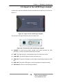
2.2 Aspect of the LA2532 logic analyzer .................................................................. 13
2.3 The hardware connections of the logic analyzer ................................................ 14
2.4 Data compression algorism ................................................................................ 15
2.5 System requirements ......................................................................................... 16
2.5.1 Minimum requirements ............................................................................ 16
2.5.2 Recommended PC platform ..................................................................... 16
Chapter 3: Software installations ............................................................... 17
3.1 Software installations ......................................................................................... 17
3.1.1 Installing the ZlgLogic Software ............................................................... 17
3.1.2 Installing the LA2532 driver ..................................................................... 20
3.2 Running the logic analyzer program .................................................................. 22
3.2.1 First time running the software after installation ....................................... 22
3.2.2 Running the software in normal situation ................................................. 23
Chapter 4: Quick start tutorial .................................................................... 24
4.1 Introduction of the experiment............................................................................ 24
4.2 Frequency measurements ................................................................................. 25
4.3 Bus activity measurements ................................................................................ 28
4.4 SPI transmission measurements ....................................................................... 31
4.5 SPI data analysis ............................................................................................... 33
Contents
.
Please visit our Website:
www.embedtools.com
广州致远电子有限公司
销售部 T:020-22644372
Contents
©2007
Guangzhou
ZHIYUAN Electronics CO., LTD . All rights reserved.
4.6
Trigger
settings ..................................................................................................
35
4.7 Plug-in trigger ..................................................................................................... 36
Chapter 5: Menu descriptions .................................................................... 39
5.1 Operation window .............................................................................................. 39
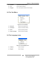
5.2 The File menu .................................................................................................... 40
5.3 The Record menu .............................................................................................. 41
5.4 Setup menu........................................................................................................ 42
5.5 The Analyser menu ............................................................................................ 43
5.6 The View Menu .................................................................................................. 44
5.7 The Window menu ............................................................................................. 44
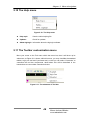
5.8 The Tool Menu ................................................................................................... 45
5.9 The Language menu .......................................................................................... 45
5.10 The Help menu ................................................................................................ 46
5.11 The Toolbar customization menu ...................................................................... 46
5.12 The waveform viewer assistant menus ............................................................ 47
5.12.1 Waveform viewer right click drop down menu ........................................ 47
5.12.2 Waveform selection drop down menu .................................................... 48
5.13 Waveform files and Bus/Signal assistant menus.............................................. 48
5.13.1 Waveform file right click drop down menu.............................................. 48
5.13.2 Bus/Signal right click drop down menu .................................................. 49
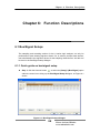
Chapter 6: Function Descriptions .............................................................. 50
6.1 Bus/Signal Setups .............................................................................................. 50
6.1.1 Quick guide on bus/signal setup .............................................................. 50
6.1.2 Dialogue Options ..................................................................................... 51
6.1.3 Details on setting a Bus/Signal ................................................................ 52
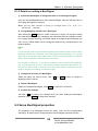
6.2 Setup Bus/Signal properties............................................................................... 52
6.2.1 Quick guide on bus/signal properties setup ............................................. 53
6.2.2 Dialogue options ...................................................................................... 53
6.2.3 Details on sampling setups ...................................................................... 54
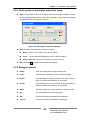
6.3 Sampling setup .................................................................................................. 54
6.3.1 Quick guide on sampling setups .............................................................. 55
6.3.2 Dialogue Options ..................................................................................... 55
6.3.3 Details on sampling setups ...................................................................... 56
6.4 Trigger setup ...................................................................................................... 57
6.4.1 Quick guides on trigger setup .................................................................. 57
6.4.2 Dialogue options ...................................................................................... 58
6.4.3 Details on trigger setup ............................................................................ 59
6.5 Run and Stop ..................................................................................................... 63
6.6 Add markers ....................................................................................................... 63
6.6.1 Quick guides on adding a new marker ..................................................... 63
6.6.2 Dialogue options ...................................................................................... 64
6.6.3 Details on adding a new marker............................................................... 64
6.7 Finding markers ................................................................................................. 65
Contents
.
Please visit our Website:
www.embedtools.com
广州致远电子有限公司
销售部 T:020-22644372
Contents
©2007
ZHIYUAN
Electronics
CO.,
LTD . All rights reserved.
6.7.1Guangzhou
Quick guides
on finding
markers
..............................................................
65
6.7.2 Dialogue options ...................................................................................... 66
6.7.3 Details on finding a marker ...................................................................... 66
6.8 Add auto measurements .................................................................................... 67
6.8.1 Quick guides on adding a new auto measurement .................................. 67
6.8.2 Dialogue options ...................................................................................... 67
6.8.3 Details on adding a new measurement .................................................... 68
6.9 Data searching ................................................................................................... 68
6.9.1 Quick guides on data searching ............................................................... 68
6.9.2 Dialogue options ...................................................................................... 69
6.9.3 Details on data searching......................................................................... 69
6.10 Waveform viewer setups .................................................................................. 70
6.10.1 Quick guides on waveform viewer setups .............................................. 70
6.10.2 Dialogue options .................................................................................... 71
6.10.3 Details on setting the waveform viewer .................................................. 71
6.11 Toolbar customization ....................................................................................... 72
6.11.1 Quick guide on toolbar customization .................................................... 72
Chapter 7: Detailed trigger guides ............................................................. 74
7.1 12 types of fast triggers ...................................................................................... 74
7.1.1 Trigger Immediately ................................................................................. 74
7.1.2 Rising edge trigger ................................................................................... 75
7.1.3 Falling edge trigger .................................................................................. 76
7.1.4 Edge trigger ............................................................................................. 76
7.1.5 Data value trigger..................................................................................... 76
7.1.6 Data queue trigger ................................................................................... 77
7.1.7 Data value and rising edge trigger ........................................................... 78
7.1.8 Data value and falling edge trigger .......................................................... 79
7.1.9 Hold time trigger....................................................................................... 79
7.1.10 Data arrival and delay trigger ................................................................. 80
7.1.11 Data passed and delay trigger ............................................................... 80
7.1.12 Data occurrence trigger ......................................................................... 80
7.2 Visual trigger setup ............................................................................................ 81
7.3 Plug-in trigger setup ........................................................................................... 82
7.4 Advanced trigger setup ...................................................................................... 82
7.4.1 Detailed Descriptions ............................................................................... 83
7.4.2 Notice on usage ....................................................................................... 84
7.5 Examples for advanced trigger setup ................................................................. 88
Chapter 8: Plug-in Analysis ........................................................................ 91
8.1 Plug-in Overviews .............................................................................................. 91
8.2 The meaning and classification of plug-in .......................................................... 92
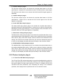
8.2.1 Bus Analyzer plug-ins .............................................................................. 92
8.2.2 Protocol analysis plug-in .......................................................................... 93
8.3 Descriptions on Analysis plug-ins ....................................................................... 94
Contents
.
Please visit our Website:
www.embedtools.com
广州致远电子有限公司
销售部 T:020-22644372
Contents
©2007
Guangzhou
ZHIYUAN
Electronics CO., LTD . All rights reserved.
8.4
Adding
a new plug-in
..........................................................................................
95
8.5 General steps to use a plug-in ........................................................................... 96
8.6 Notice on using plug-ins ..................................................................................... 96
Chapter 9: Bus analysis plug-ins ............................................................... 98
9.1 Overview on Bus analysis .................................................................................. 98
9.2 The 1-Wire bus analysis plug-in ......................................................................... 98
9.2.1 1-Wire Bus Analysis setup options ........................................................... 99
9.2.2 Detailed descriptions ................................................................................ 99
9.3 A/D Conversion Analysis plug-in ...................................................................... 101
9.3.1 A/D Conversion setup options ................................................................ 101
9.3.2 Detailed descriptions .............................................................................. 102
9.3.3 Notice on usage ..................................................................................... 104
9.4 I2C Bus analysis plug-in ................................................................................... 105
9.4.1 I2C Bus Analysis setup options .............................................................. 105
9.4.2 Detailed descriptions .............................................................................. 106
9.4.3 Notice on usage ..................................................................................... 109
9.5 Experiment on using I2C Bus Analysis plug-in ................................................. 109
9.5.1 Goal of the experiment........................................................................... 109
9.5.2 Program list of the experiment ............................................................... 110
9.5.3 Steps for data recording ......................................................................... 112
9.5.4 Steps for data analysis ........................................................................... 113
9.6 SPI Bus analysis plug-in .................................................................................. 117
9.6.1 SPI Bus Analysis setup options ............................................................. 117
9.6.2 Detailed descriptions .............................................................................. 118
9.6.3 Notice on usage ..................................................................................... 122
9.7 Example on using SPI Bus Analysis plug-in ..................................................... 122
9.7.1 Goal of the experiment........................................................................... 122
9.7.2 Program list ............................................................................................ 122
9.7.3 Steps for recording ................................................................................. 124
9.7.4 Steps for analysis ................................................................................... 126
9.8 SSI Bus Analysis plug-in .................................................................................. 128
9.8.1 SSI Bus Analysis setup options ............................................................. 128
9.8.2 Detailed descriptions .............................................................................. 129
9.9 UART Bus Analysis plug-in .............................................................................. 132
9.9.1 UART Bus Analysis setup options.......................................................... 132
9.9.2 Detailed descriptions .............................................................................. 133
9.9.3 Notice on usage ..................................................................................... 137
9.10 UART Bus analysis example .......................................................................... 137
9.10.1 Goal of the experiment ......................................................................... 137
9.10.2 Program lists ........................................................................................ 137
9.10.3 Steps for recording ............................................................................... 139
9.10.4 Steps for analysis ................................................................................. 141
9.11 Manchester Coding Analysis plug-in .............................................................. 141
9.11.1 Manchester Coding Analysis setup options .......................................... 142
Contents
.
Please visit our Website:
www.embedtools.com
广州致远电子有限公司
销售部 T:020-22644372
Contents
©2007
Guangzhou
ZHIYUAN Electronics
CO., LTD . All rights reserved.
9.11.2
Detailed descriptions
............................................................................
143
9.12 Modified Miller coding analysis plug-in ........................................................... 146
9.12.1 Modified Miller Coding Analysis setup options ..................................... 146
9.12.2 Detailed functions and notice on usage ............................................... 147
Chapter 10:
Plug-in Triggers................................................................. 150
10.1 Plug-in trigger overview.................................................................................. 150
10.2 General steps to use a plug-in trigger ............................................................ 151
10.3 1-Wire Bus Analysis plug-in Trigger ............................................................... 151
10.3.1 The Trigger setup for 1-Wire Bus ......................................................... 151
10.3.2 Detailed descriptions ............................................................................ 152
10.4 I2C Bus Analysis Plug-in trigger...................................................................... 153
10.4.1 I2C Bus Analysis plug-in trigger setup interface ................................... 153
10.4.2 Detailed descriptions ............................................................................ 153
10.5 I2C Plug-in trigger experiment ........................................................................ 155
10.5.1 Goal of the experiment ......................................................................... 155
10.5.2 Steps for trigger setup .......................................................................... 156
10.6 SPI Bus Analysis plug-in trigger ..................................................................... 159
10.6.1 SPI Bus Analysis plug-in trigger setup ................................................. 159
10.6.2 Detailed descriptions ............................................................................ 159
10.7 SPI Bus Analysis plug-in trigger example....................................................... 161
10.7.1 Goal of the experiment ......................................................................... 161
10.7.2 Steps for trigger setup .......................................................................... 161
10.8 SSI Bus Analysis plug-in trigger ..................................................................... 163
10.8.1 SSI Bus Analysis plug-in trigger setup ................................................. 163
10.8.2 Detailed descriptions ............................................................................ 163
10.9 UART Bus Analysis plug-in trigger ................................................................. 164
10.9.1 UART Bus Analysis plug-in trigger setup ............................................. 165
10.9.2 Detailed descriptions ............................................................................ 165
10.10 UART Bus Analysis plug-in trigger experiment............................................. 167
10.10.1 Goal of the experiment ....................................................................... 167
10.10.2 Detail descriptions.............................................................................. 167
Chapter 11:
Protocol Analysis plug-in ................................................. 169
11.1 Protocol analysis plug-in Overviews ............................................................... 169
11.2 CF Card True IDE Mode Analysis plug-in ....................................................... 169
11.2.1 CF Card decoding setup options .......................................................... 170
11.2.2 Detailed descriptions ............................................................................ 171
11.2.3 Notice on usage ................................................................................... 175
11.3 Modbus Protocol Analysis plug-in .................................................................. 176
11.3.1 Modbus protocol decoding setup options ............................................. 176
11.3.2 Detailed descriptions ............................................................................ 178
11.3.3 Notice on usage ................................................................................... 182
11.4 SD Card Protocol analysis plug-in .................................................................. 183
11.4.1 SD Card protocol decoding setup dialogue .......................................... 183
Contents
.
Please visit our Website:
www.embedtools.com
广州致远电子有限公司
销售部 T:020-22644372
Contents
©2007
Guangzhou
ZHIYUAN Electronics
CO., LTD . All rights reserved.
11.4.2
Detailed descriptions
............................................................................
184
11.4.3 Notice on usage ................................................................................... 187
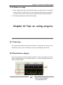
Chapter 12:
Tips on using plug-ins ...................................................... 187
12.1 Overview ........................................................................................................ 187
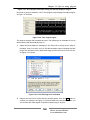
12.2 Deactivate a plug-in ....................................................................................... 187
12.3 Reactivate a plug-in ....................................................................................... 189
12.4 Using multiple plug-ins in one project ............................................................ 190
Chapter 13:
Special Functions ............................................................. 191
13.1 Digital filters ................................................................................................... 191
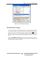
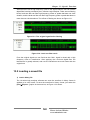
13.2 Loading a saved file ....................................................................................... 192
13.3 Logic pen ....................................................................................................... 196
13.4 Cymometer .................................................................................................... 197
13.5 Automatic upgrades ....................................................................................... 199
13.6 Automatic measurements............................................................................... 202
13.7 Tips on using the logic analyzer ..................................................................... 203
Chapter 14:
Supports & guarantees..................................................... 207
14.1 Frequently Asked Questions and answers ..................................................... 207
14.2 Technical supports ......................................................................................... 209
14.3 Feedbacks ..................................................................................................... 210
Appendix I: Tool bar icons ........................................................................ 210
Appendix II: Hotkey lists ........................................................................... 212
Appendix III ISO9000 Certificates ............................................................. 213
Contents
.
Please visit our Website:
www.embedtools.com
广州致远电子有限公司
销售部 T:020-22644372 F:020-38601859
©2007 Guangzhou ZHIYUAN Electronics CO., LTD . All rights reserved.
Chapter 1: Product Introduction
Due to the fast development of the electronic devices, the digital circuit designing
takes up more and more percentage in the total electronic devices developments,
thus, how to verify and check a digital circuit is getting more and more important
today.
Now, ZHIYUAN Electronics brings you a brand new LA series logic analyzer to
assist your development in this critical area. It contains many new and creative
technologies, leading the evolution of analyzer functions and techniques. The LA
series logic analyzer uses the PC as its displaying platform, and communicates with
the devices through USB ports. It also supports the most popular Windows system
and provides with a beautiful and convenient user interface. With its powerful
triggering abilities, user can easily find out even slightest errors within the system;
with its complete bus and protocol analyze capabilities, user can analyze their
products without going deep into any details of the protocols; with its highly effective
compress algorism, user can obtain more information and save more sampling
points to process more data; also, with its automatic and online upgrade capability,
user can get the newest technologies and updates anytime and anywhere.
LA2532 logic analyzer adopts the advanced large scale integrated circuits and
mixes with many brand new technologies of the embedded systems, such as
USB2.0, CPLD, and FPGA; also supports the USB powered and the Plug & Play
technology. Comparing to the traditional logic analyzer, it has the advantages on its
high performance, low costs, easy to carry, convenient on usage, and good
extendibility; it’s the best choice for you to replace your old or traditional logic
analyzers.
LA2532 is a 100M, 32 channels high performance logic analyzer that can be use to
perform the developing, measuring, analyzing, and debugging works; it’s a powerful
device designed for developing or verification engineers in electronic field, and also
a convenient tool for high school research or teaching teams. It’s an electronic
instrument with many brand new measurement methods.
.
1
Please visit our Website:
www.embedtools.com
广州致远电子有限公司
销售部 T:020-22644372 F:020-38601859
The major advantage of the LA2532 is listed as below:
©2007 Guangzhou ZHIYUAN Electronics CO., LTD . All rights reserved.
z Provides with flexible and creative trigger techniques to speedup and simplify
your measurement procedure.
z
Provides edge, value, pattern and many other triggering mode; convenient for
usage. Also provides a data compress algorism to extend the recording depth
and increase the precision of the data sampling.
z
Provides with a dedicated bus and protocol analysis function, which greatly
simplifies your analysis on data related to UART, SPI, I2C, and SSI buses and
their related protocols.
z
Provides a humanize software interface that integrated with many useful
functions, such as signal measurement, triggering setting, dynamic helps,
software upgrade and etc.
z
Supports multi-task structure; you can do the data measurement, comparison
and observations on different data at a same time.
z
Supports multiple export file formats, you can perform the off-line analysis
easily.
z
Flexible frequency settings, breaks out the 125 scale limits and make the
measurement more precisely.
z
Contains a high performance measurement core, does not depend on high
performance PC.
z
USB 2.0 high speed interface, with PnP (Plug & Play) support.
z
Smaller size and beautiful shape, easy to carry.
z
With its dynamic hardware upgrade mechanism, you can keep your
measurement technique up to date anytime. And its replaceable analog front
end design allows the upgrading of the hardware and enhances your analyzer
with stronger functions. All these make your investments more valuable and
worth the price.
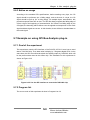
1.1 Why using a Logic analyzer
The most frequently used device in our electronics development are oscilloscopes,
but as the microprocessor develops, more and more engineers find that the original
2 or 4 channel oscilloscopes no longer satisfy their analysis requirements in the
development procedure. To meet the requirements, the multi-channel
handler---logic analyzer is invented. It not only solves the lack of channel problem,
but also provides a powerful triggering and analysis abilities; no doubt it’s a good
testing and analyzer tool for digital devices developments.
.
2
Please visit our Website:
www.embedtools.com
广州致远电子有限公司
销售部 T:020-22644372 F:020-38601859
©2007 Guangzhou
ZHIYUAN
Electronics CO., LTD . All rights reserved.
1.2 Logic
analyzer
or oscilloscope?
1.2.1 Differences between logic analyzers and oscilloscopes
The oscilloscope is a popular tool for electronic engineers; the major function of a
oscilloscope is to display the analogue characteristics, voltage scope, and the
spurious interference of a signal. But a logic analyzer is designed for digital circuits,
because of the inherence characteristics of the digital circuit, the logic analyzer will
not focus on specific voltage values and the analogue characteristic of a signal, it
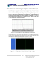
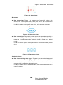
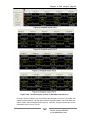
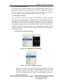
works on the aspects of voltage level. For example, Figure 1-1 shows a falling edge
of a signal displayed in oscilloscope software.
Figure 1-1: A falling edge of a signal displayed in oscilloscope
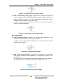
For an oscilloscope, it can measure the falling time of the voltage, voltage scope,
and the spurious interference of this signal. But for a logic analyzer, the result of the
measurement to this signal is quite different, as Figure 1-2 Shows.
Figure 1-2: A falling edge of a signal displayed in logic analyzer
.
3
Please visit our Website:
www.embedtools.com
广州致远电子有限公司
销售部 T:020-22644372 F:020-38601859
©2007
Guangzhou ZHIYUAN
Electronics CO., LTD
All rights
reserved.
1.2.2 The
measurement
methodology
of .logic
analyzers
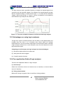
The logic analyzer used a specified frequency to sample the inputted signal, then
compare it with the threshold voltage; if the voltage of the inputted signal is greater
than the threshold voltage, it will be treat as logic “1”; if it’s less than the threshold
voltage, it will be treat as logic “0”. Figure 1-3 shows a comparison on the gathering
result between logic analyzer and oscilloscope
Figure 1-3: The result comparison between oscilloscope and logic analyzer
1.2.3 Advantages on using logic analyzers
Though some types of oscilloscope also have the ability to view digital signals, but
normally they only have 2 to 4 channels, they cannot satisfy the analysis
requirements for 5 or more channels, especially for microprocessor buses. Normally
a logic analyzer will have 16 or more channels, even over 300 channels for some
high-end product types.
Comparing to oscilloscopes, the logic analyzer has these advantages:
(1) Monitors multiple channels at a same time
(2) With good and various triggers
(3) Powerful analysis functions
1.2.4 Four application fields of logic analyzer
There are four application fields for a logic analyzer
(1) Oscilloscope
Observe the waveform to find out if there’re burrs or interferes, or check if there’s
errors on frequency.
(2) Timing measurements
Measure the timing of signals to find out conflicts or timing problems.
.
4
Please visit our Website:
www.embedtools.com
广州致远电子有限公司
(3) Assistance on analysis
销售部 T:020-22644372 F:020-38601859
©2007 Guangzhou ZHIYUAN Electronics CO., LTD . All rights reserved.
Provide additional analysis to bus signals or protocols to simplify the development
cycle.
(4) Bug finder
With its strong trigger ability, a logic analyzer can be used for error tracing or finding
hidden bugs within the system, this advantage improves the stability and reliability of
the product under development.
1.3 Application example of logic analyzer
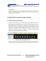
1.3.1 Multi-channel measuring
Usually an oscilloscope only has two channel inputs, so it’s incapable for most of the
multi-channel input measurements, such as SPI, SSI, Microwire and etc; but for a
logic analyzer, since it has over 16 channels, it can handle this kind of
measurements easily. For example, the SPI communication has 4 signals: CS, SCK,
SI, and SO. It’s a popular interface supported by many types of chips, such as
EEPROM, I/O Extension, reset chip, USB devices and etc.; also it was widely
applied in the electronic devices field. Figure 1-4 shows an example signal
transmitted on SPI bus recorded by a logic analyzer:
Figure 1-4: SPI measurement results
As Figure 1-4 shows, by using the logic analyzer, the SPI communications and the
relationship between data transferring and chip select signal are clear to observe.
.
5
Please visit our Website:
www.embedtools.com
广州致远电子有限公司
销售部 T:020-22644372 F:020-38601859
©2007
Guangzhou ZHIYUAN
Electronics CO., LTD . All rights reserved.
1.3.2 Bus
frequency
measurements
Most of the practical projects or designs may require peripherals, such as RAM,
FLASH, and USB interfacing chips, to extend the functionalities of the processor.
Actually, for higher performance, a microprocessor should run at a higher clock
frequency; however, as the clock frequency boost up, many strange problems also
appears, most of these issues are caused by the mismatch on the timing between
processor and different devices. To demonstrate the solutions to these issues, here
is an example on maximizing the performance of the processor when using a
SST39VF160-90 Flash chips as an external storage for LPC22xx series processors.
Figure 1-5 shows that the read-in timing on the SST39VF160-90 Flash chip and its
dynamic parameters are listed in the following Table.
Figure 1-5: The read-in timing of the SST39VF160-90
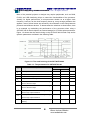
Table 1-1: The parameters for SST39VF160-90
Signal
Description
SST39VF160-90
Minimum
Unit
Maximum
TRC
Read cycle duration
90
ns
TCE
Chip enable time
90
ns
TAA
Address accessing time
90
ns
TOE
Output enable accessing time
45
ns
1
TCLZ
Time spent on CE# switch from low voltage
0
ns
0
ns
level to effective output
1
TOLZ
Time spent on OE# switch from low voltage
level to effective output
TCHZ1
Time spent on CE# switch from high voltage
30
ns
30
ns
level to high output resistance
TOHZ1
Time spent on OE# switch from high voltage
level to high output resistance
TOH1
Time spent from address modification to output
0
holding
.
6
Please visit our Website:
www.embedtools.com
ns
广州致远电子有限公司
销售部 T:020-22644372 F:020-38601859
, TCHZ
) is the
key parameter
for
In Table
1-1,
you may ZHIYUAN
find that TElectronics
©2007
Guangzhou
CO.,
LTD (T
. All
reserved
.
RC, TCE, TAA
OHZrights
data reading. If TRC, TCE, TAA does not satisfied, the data read in procedure will have
errors and also it may cause hardware damages. The TOE parameter can be ignore
here, because the OE and CE are output simultaneously in ARM structure.
Figure 1-6 shows the actual timing of the LPC22xx to read in data from a external
Flash memory. With a logic analyzer, it’s quite easy to measure and find out whether
the time sequencing of the read operation from the microcontroller matches the
flash device requirements. As we can see, the TCR read cycle duration is 130 ns, it’s
bigger than the minimum time required, which is 90ns. The TCHZ (TOHZ) is 40ns,
which also satisfies the flash requirements. Since all major requirements are
matched, the reliability of the flash reading operation should be guaranteed. Also,
form this measurement, you may find that the Flash reading operation can be
configured to a bit faster to improve the system performance.
Figure 1-6: FLASH read timing sequence of a PHLIPS ARM7 processor
The cooperating issue of the timing sequence is especially important when using the
bus extension mode to connect with functional devices; this makes the logic
analyzer even more important on the time sequencing analysis for a bus, also
makes it a strong assurance to the healthy running of the system.
1.3.3 Trigger ability
Another great advantage of a logic analyzer is its versatile trigger setups.
Comparing to oscilloscopes which only have two triggering method, the level and
edge trigger; the logic analyzer has much more options available on triggers.
Generally, a complete analyzer should have the following triggers.
.
7
Please visit our Website:
www.embedtools.com
广州致远电子有限公司
销售部 T:020-22644372 F:020-38601859
Table 1-2: Common triggers of a logic analyzer
©2007 Guangzhou ZHIYUAN Electronics CO., LTD . All rights reserved.
Name
Edge trigger
Descriptions
Applications
When a transition takes place on the
Generally use this way to trigger at the
selected input signal (rising edge,
change of a signal, such as read, write
following edge or double edge),
signals.
trigger and start the recording.
State trigger
Edge & state trigger
When the selected input signal or
Often use it to trigger at the appearance
pattern
of a specific data value, such as output
matches
a
given
state,
trigger and start the recording.
signal states.
When the state of the selected input
Often use it to trigger at the appearance
signal and the transition of the signal
of a specific data value, such as the read
satisfy certain conditions, trigger and
or write operations on specific address.
start the recording
Pulse trigger
Counter trigger
When pulses with a specified width
Often use it to trigger at the occurrence
on a signal last for a specific
of some specific error states such as a
duration,
wrong width of the PWM output; or use it
trigger
and
start
the
recording
for burr analysis.
When the occurrence counting of a
Often use this to detect some specific
specific data value on a signal reach
errors, such as program output errors.
a specified number, trigger and start
the recording
Sequential trigger
Duration trigger
When the specified data sequence
Often use it to detect specific operations,
appears on the selected input signal,
such as communication symbols based
trigger and start the recording
on a protocol.
When a specific state appear on the
Often use it to trace the after effects of a
selected
a
specific error or event; such as tracing a
specified duration of time and then
data transmission error and the following
trigger and start recording
events after its occurrence.
input
signal,
delay
With the abovementioned triggers, one can easily find out bugs hidden in massive
data or information. The listed triggers are just general methods provided in most
common logic analyzers; some advanced logic analyzers, such as LA2532 logic
analyzer can also provide some special trigger controls, such as visual trigger and
combined trigger.
1.3.4 Capabilities on analysis
The analysis of an oscilloscope is focus on the frequency, duty ratio and peek
voltages of the target signal input, and the analysis can only perform to a single
signal. But a logic analyzer is capable to perform analysis on multiple signals.
For example, both the oscilloscope and logic analyzer can measure the UART data
derived from MCU; Figure 1-7 shows the measuring result of an oscilloscope. From
this figure you can only observe the time scales and the voltage values, it contains
no information about the data contents about the signal.
.
8
Please visit our Website:
www.embedtools.com
广州致远电子有限公司
销售部 T:020-22644372 F:020-38601859
©2007 Guangzhou ZHIYUAN Electronics CO., LTD . All rights reserved.
Figure 1-7: The measurement result from a oscilloscope
As a comparison, the measurement result of the LA2532 logic analyzer is shown in
Figure 1-8. Not only can the logic analyzer measure the voltage and time, but also it
can perform practical analysis to data by using its plug-ins. Just fill in some
parameters related to the Serial UART bus, then the logic analyzer can perform
analysis to the signal based on UART transmission protocol, and display the result
on screen, so that developers can study the transferring data in a more directly way.
Figure 1-8: The UART data measurement result from a logic analyzer
The UART data measurement is just a small case. A good logic analyzer can also
perform analysis to serial port or parallel port data, converting the waveforms to data
values based on bus specifications, For example, the LA2532 supports the analysis
to Serial UART, I2C, SPI, SSI, 1-wire and other buses.
An advanced logic analyzer can even analyze data based on higher layer protocols.
For example, the LA2532 logic analyzer can perform analysis to the SD/MMC card
data on SPI mode, CF card data on TrueIDE mode, Modbus protocol data and etc. It
can display the results directly on screen, quite convenient for user to observe and
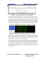
compare it with the original signals. Figure 1-9 shows an example of analysis on SD
card transmissions.
.
9
Please visit our Website:
www.embedtools.com
广州致远电子有限公司
销售部 T:020-22644372 F:020-38601859
©2007 Guangzhou ZHIYUAN Electronics CO., LTD . All rights reserved.
Figure 1-9: SD card transmission protocol analysis
The CS, SCK, MOSI, MISO in Figure 1-9 is the original data in communications,
DataIn, DataOut are the result of the SPI bus analysis, and InCmd, OutCmd are the
result of the protocol analysis.
1.3.5 Error captures
The powerful and versatile triggers of logic analyzer can be used to capture bugs
and errors of the system. Take the 80C51 processor as an example, if a data access
operation is out of the internal memory segments, the processor will signal the
PSEN pin to activate the access to external memories. So, use the logic analyzer
and set a trigger upon the PSEN signal, then the logic analyzer can record the
accessing operations to external memories, so that engineers can analyze the result
and find out errors. Generally, the code segment of 80C51 processor is 0x0000 ~
0x3fff and the address in PC of a running program should not exceed it, or else it
should be a run-away error. To capture a run-away error, you can use the advanced
triggers provided by the LA2532 series logic analyzer, just set the trigger condition to
Address>0x3fff and PSEN has a falling edge, then, when the processor is fetching
an instruction out of the 0x0000~0x3fff limit, the logic analyzer will be triggered to
record the error states.
.
10
Please visit our Website:
www.embedtools.com
Chapter 2: Hardware introductions
Chapter 2: Hardware introductions
2.1 Features of LA2532 Logic analyzer
2.1.1 Feature 1: Logic analyzer
z
Maximum sample rate:
200MHz
z
Real time waveform viewer:
Supported
z
Maximum storage depth:
1M Sampling points/Channel
z
Data compression abilities:
Supported
z
Input impedance:
IMΩ
z
Threshold voltage:
-4V~4V (two channel adjustable)
z
Input signal voltage range:
-5V~5V
z
USB protocol support:
USB 2.0 (High speed, Full speed)
z
Free Trigger position configuration:
Supported
z
Fast trigger configuration:
Supports 12 types of fast triggers
(Immediately trigger, positive edge trigger, negative edge trigger, edge trigger, specific value
trigger, data queue trigger, specific value and positive edge trigger, specific value and
negative edge trigger, data width trigger, arrival delay trigger, pass over delay trigger, and
data occurrence counting trigger respectively)
.
z
Visual triggering:
Supported
z
Plug-in triggering:
Supported
z
User-defined advance triggering:
Supported
z
Automatic upgrades:
Supported
11
Please visit our Website:
www.embedtools.com
Chapter 2: Hardware introductions
z
Multilanguage support:
Supported
z
Multi documentation structure:
Supported
z
Waveform printing:
Supported
z
Supported system:
Windows 2000, Windows XP
2.1.2 Feature 2: Bus analyzer
z
UART Bus analysis:
Supported
z
I2C Bus analysis:
Supported
z
SPI Bus analysis:
Supported
z
SSI Bus analysis:
Supported
z
1-Wire Bus analysis:
Supported
z
A/D Conversion analysis:
Supported
z
Manchester coding analysis:
Supported
z
Modified Miller Coding analysis:
Supported
2.1.3 Feature 3: Protocol analyzer
z
Modbus protocol analysis:
Supported
z
CF Card protocol analysis:
Supported
z
SD/MMC card protocol analysis:
Supported
2.1.4 Feature 4: Cymometer
z
10Hz~50MHz
Measuring range:
2.1.5 Feature 5: Logic pen
z
.
1ms
Sampling period:
12
Please visit our Website:
www.embedtools.com
Chapter 2: Hardware introductions
2.2 Aspect of the LA2532 logic analyzer
LA2532 has a white and beautiful aluminous metal shell; the aspect of it is shown as
Figure 2-1:
Figure 2-1: Aspect of the LA2532 logic analyzer
The left side of the logic analyzer is shown as Figure 2-2.
Figure 2-2: The left side of the LA2532 logic analyzer
.
z
POWER: 5v power source inputs. Usually, the LA2532 supports the USB
powered, so it may not need this power input normally.
z
USB: The USB2.0 port for communications with PC and power source.
z
POW LED: This red LED lights up when the power is on
z
USB LED: This green LED lights up when data is transferring through the USB
bus.
z
RUN LED: This yellow LED lights up when the analyzer is working normally.
z
RST Button: Press it to reset the logic analyzer.
13
Please visit our Website:
www.embedtools.com
Chapter 2: Hardware introductions
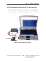
2.3 The hardware connections of the logic analyzer
Take out the USB cables accompanied with the logic analyzer, connect the B type (a
square shape port) side of the USB cable to the USB port of the LA2532, and then
connect the other side of the USB cable (a rectangle shape port) to the PC’s USB a
type slot. Keep the power in “OFF” state during this procedure.
Data sampling
Figure 2-3: The connections of the hardware
.
14
Please visit our Website:
www.embedtools.com
Chapter 2: Hardware introductions
2.4 Data compression algorism
LA2532 has an extraordinary data compression algorism that can perform real-time
compression to the recording data without lowering the performance or reducing the
number of sampling channels. It really achieves the real-time and complete data
compression and can be activated simply by selecting the “Compress” option within
the Sampling clip of the Setup window.
The data compression algorism adopted by LA2532 is highly effective; under the
maximum compress rate, the sampling data depth after compression can reach 2G
(29) times greater than the original data depth without compression, this greatly
improve the maximum time period of sampling. For example, when using a 1000
KHz sampling rate to sample a 100 KHz signal, the original recording time without
compression will be 32 seconds, but the recording time with data compression can
be over 80 seconds, this is more than twice of the recording time without
compression.
The data compression adopts a non-linear method, and the compression rate can
be adjusted to a best value automatically to meet different situations, but the lowest
compression rate will not lower than 1 (This means that the recorded sample points
is more than or equal to the original 32Kbits without compression).
The following figures show that an example on external bus data recording for an
8051 processor. When using the traditional recording method without data
compression, the recorded time is less than 400us, but with the data compression
method, the recorded time can be extended over 4ms, so the recordable time is 10
times longer than using the traditional method. Comparing two figures, you can find
that the precision of the record does not change when using data compressions.
Before data compression:
Figure 2-4: Before data compression
.
15
Please visit our Website:
www.embedtools.com
Chapter 2: Hardware introductions
After data compression:
Figure 2-5: After data compression
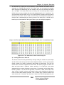
2.5 System requirements
2.5.1 Minimum requirements
z
600MHz or faster CPU
z
128MB or more memory
z
30MB or more free hard disk space
z
USB1.1 or USB2.0 interface
z
1024×768 or higher resolution monitor, 16 bit color or upper
z
Windows 2000+SP4 or later operation system
z
IE6.0 or later version browser
2.5.2 Recommended PC platform
.
z
1GHz or faster CPU
z
256MB or more memory
z
100MB or more free hard disk space
z
USB1.1 or USB2.0 interface
z
1024×768 or higher resolution monitor, 16 bit color or upper
z
Windows XP+SP2 or later operation system
z
IE6.0 or later version browser.
16
Please visit our Website:
www.embedtools.com
Chapter 3: Software installations
Chapter 3: Software installations
3.1 Software installations
3.1.1 Installing the ZlgLogic Software
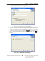
Please insert the CD accompanied with the LA2532 logic analyzer into your
CD-ROM driver, and then start the installation following the instructions listed below.
1. Double click on the
Figure 3-1 shows.
icon to bring up the “Preparing to install” dialogue, as
Figure 3-1: Preparing to install
.
17
Please visit our Website:
www.embedtools.com
Chapter 3: Software installations
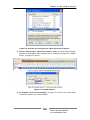
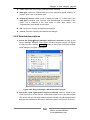
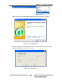
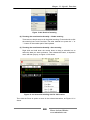
2. After the system check is completed, click “Next” to proceed.
Figure 3-2: The installation startup dialogue
3. Read the license agreement carefully, tick the “I Accept…” option then click
“Next” to proceed.
Figure 3-3: The License Agreement dialogue
.
18
Please visit our Website:
www.embedtools.com
Chapter 3: Software installations
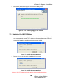
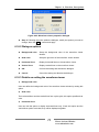
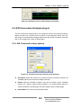
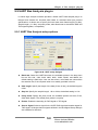
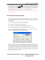
4. Fill in the user name and organization then select the authorization type within
the Customer Information window, click “Next” to proceed.
Figure 3-4: The Customer Information dialogue
5. As Figure 3-5 shows, the software will install to its default folder if user does not
change the installation path within the Destination Folder window; if user wants
to change the destination folder, just click the “Change” button and change the
path in a file browser dialogue; after setting your installation path, click “Next” to
proceed.
Figure 3-5: The Destination Folder dialogue
.
19
Please visit our Website:
www.embedtools.com
Chapter 3: Software installations
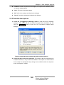
6. If every thing is OK, the program will start the installing of files.
Figure 3-6: The “Installing zlglogic 2.0” window
3.1.2 Installing the LA2532 driver
1. After the installation of the zlglogic2.0 software, a driver installation dialogue will
pop up automatically to ask you for hardware driver installations, as Figure 3-7
shows, click “Install” to install the device drivers for LA2532.
Figure 3-7: LA2532 driver installations
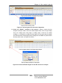
2. Figure 3-8 shows that the driver installation is in progress.
Figure 3-8: LA2532 driver installations
! Notice: DO NOT connect the logic analyzer when installing the drivers.
○
.
20
Please visit our Website:
www.embedtools.com
Chapter 3: Software installations
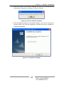
3. After few minutes, an information dialogue will pop up to indicate that the
LA2532 driver installation is complete; as Figure 3-9 shows.
Figure 3-9: Driver installation complete
4. Then the zlglogic software is successfully installed, if you tick the “Launch the
program” option, then after the installation it will start the running of zlglogic2.0
software automatically.
Figure 3-10: Installation complete
.
21
Please visit our Website:
www.embedtools.com
Chapter 3: Software installations
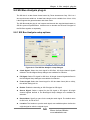
3.2 Running the logic analyzer program
3.2.1 First time running the software after installation
When the installation is complete, you may tick the “Launch the program” option to
start the program directly. Then the software interface will run automatically after the
installation.
Figure 3-11: The zlglogic software interface
If your PC is not connected with the LA2532 logic analyzer, then a offline status will
show on the status bar indicating that the connection is not ready
Figure 3-12: Offline status
.
22
Please visit our Website:
www.embedtools.com
Chapter 3: Software installations
3.2.2 Running the software in normal situation
Normally, there are two ways to start the software interface
a)
Double click the shortcut on you desktop
b)
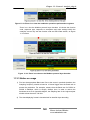
Select the program under the “Start”Æ”zlgmcu Logic Analyzer” menu
Figure 3-13: Launch the program from start menu
.
23
Please visit our Website:
www.embedtools.com
Chapter 4: Quick start tutorial
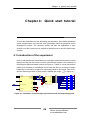
Chapter 4: Quick start tutorial
To meet the requirements of the technology developments, MCU based embedded
system designs takes up more and more percentage within the electronic device
development projects. The following section will take the application of logic
analyzer on a MCU system as an example to illustrate how to use the LA2532 logic
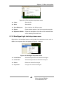
analyzer
4.1 Introduction of the experiment
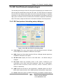
Here we will describe the measurement of a flow light experiment board as a tutorial
example to help your about how to use the LA2532 logic analyzer. The schematic of
the flow light experiment board is shown as Figure 4-1. Within it, we can see that the
P89LPC913 processor is controlling 8 LED through the SPI bus, to figure out what’s
happening on the board, we place 12 measuring probes on the circuit, CH0~CH11;
and the measuring location of each probe is marked with a sign “
U1
9
6
3
CH0
8
P1.0/TXD
P1.1/RXD
U2
P0.6
P2.5/SPICLK
P2.2/MOSI
P2.3/MISO
CS
CLK
CH1
CH2
DATO
CH3
VCC33
RST/P1.5
P0.5
P0.4
P0.2
11
12
13
8
1
2
14
9
7
CP
A
B
VCC
MR
GND
74HC164
Q0
Q1
Q2
Q3
Q4
Q5
Q6
Q7
3
4
5
6
10
11
12
13
CH4
CH5
CH6
CH7
CH8
CH9
CH10
CH11
R1
470
VCC33
LED1
R2
470
LED2
R3
470
LED3
R4
470
LED4
R5
470
LED5
R6
470
LED6
R7
470
LED7
R8
470
LED8
CLKO/XTAL2/P3.0
VDD
7
5
2
1
14
” in Figure 4-1.
XTAL1/P3.1
VSS
10
VCC33
4
P89LPC913
Figure 4-1: Schematic of the flow light experiment board with measuring points
.
24
Please visit our Website:
www.embedtools.com
Chapter 4: Quick start tutorial
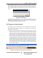
Connect the logic analyzer to the PC with a USB cable and run the logic analyzer
software zlglogic2.0; then the main interface of the software appears, as Figure 4-2
shows. Check the status bar to ensure the connection is OK, because the device
cannot operate properly when disconnected (an “Offline” status as Figure 4-2
shows).
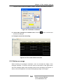
Figure 4-2: The Offline state
We separate the whole measurement to the system into several steps; they are
Frequency measurements, Bus activity measurements, SPI transmission
measurements and SPI data analysis respectively.
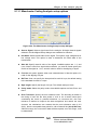
4.2 Frequency measurements
The oscillator priming of the RC oscillator circuit is a prerequisite to ensure the MCU
work normally. Using the logic analyzer, user can easily find out whether the
oscillator circuit works properly.
z
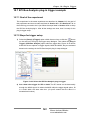
Step 1: Connect the CH0 probe of Pod A to the crystal oscillator pin (the CH0
location is shown in Figure 4-1). In normal situations, the internal RC circuit will
initiate the oscillation; through the logic pen and Cymometer function of LA2532
logic analyzer, we can observe the frequency and the state of this signal, as
Figure 4-2 shows. The CH0 bit within the logic pen has a
sigh, showing that
there are fluctuating waves within this channel, and the Cymometer shows that
the signal frequency of CH0 signal is 3.773MHz, which is nearly the half of the
internal oscillating frequency of P89LPC813 (the RC oscillator is not precise
enough); and the result showing that the oscillator is running normally. Notice
that if the logic pen is directly used to measure an oscillation output pin, the
threshold voltage should be configured; details on setting the threshold voltage
can be found in Chapter 13.
Figure 4-3: The results on measuring the crystal oscillator
.
25
Please visit our Website:
www.embedtools.com
Chapter 4: Quick start tutorial
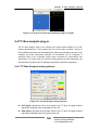
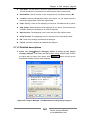
z
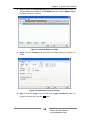
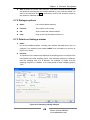
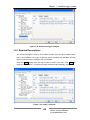
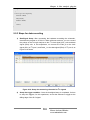
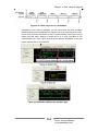
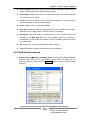
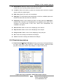
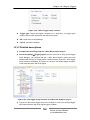
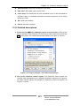
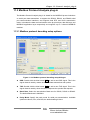
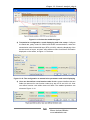
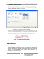
Step 2: Select the [Setup]Æ[Bus/Signal] option with the menu bar to bring up
the Bus/Signal setup dialogue, delete MyBus0 bus and rename Mybus1 signal
to XTAL, as Figure 4-4 shows.
Figure 4-4: Rename Mybus1 to XTAL
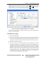
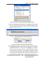
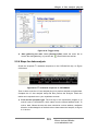
z
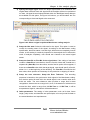
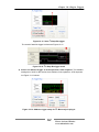
Step3: Click the Sampling clip and keep the default settings, as Figure 4-5
shows
Figure 4-5: Sampling frequency settings
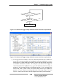
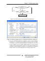
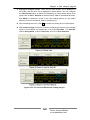
z
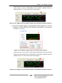
.
Step 4: Click the Trigger clips and select the Trigger immediately option, as
Figure 4-6 shows; then click the OK button.
26
Please visit our Website:
www.embedtools.com
Chapter 4: Quick start tutorial
Figure 4-6: Trigger setup for frequency measurements
z
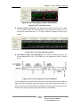
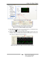
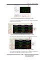
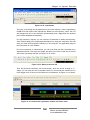
Step 5: click the run button ( , run once) within the tool bar, then the logic
analyzer will display the waveform of the measuring signal, as Figure 4-7.shows.
When you move the mouse cursor onto the waveforms, the software will display
a small notice about the signal, as Figure 4-7 shows. The logic analyzer
software will give out an instant information notes about the signal segment
where the cursor points. As Figure 4-7 shows, the high voltage level of XTAL
signal, where the cursor is pointing, lasts 140ns.
Figure 4-7: The measurement result of XTAL signal
.
27
Please visit our Website:
www.embedtools.com
Chapter 4: Quick start tutorial
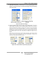
4.3 Bus activity measurements
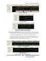
z
Step1: Connect the CH4~CH11 probes of Pod A to the Q0~Q7 pin of the
74HC164 chip respectively, as Figure 4-1 shows. Then Select the [Setup]
Æ[Bus/signal] option within the menu to bring up the Bus/Signal setup
dialogue, then click the “Insert” button to add a bus named LED, as Figure 4-8
shows. Then click “OK“ to proceed.
Figure 4-8: Add a LED bus
z
Step 2: click the run ( , run once) within the tool bar, the measurement result
of the logic analyzer is shown as Figure 4-9
Figure 4-9: XTAL and LED measurement results
.
28
Please visit our Website:
www.embedtools.com
Chapter 4: Quick start tutorial
z
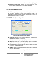
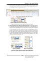
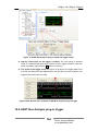
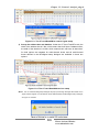
Step 3: Since the XTAL has much higher frequency than LED, so it’s hard to
observe them together, for the convenience in observing the LED bus, you
need to delete the XTAL signal and observe the LED signal alone, this action is
similar to the deletion of MyBus0. Because LA2532 has data compression
ability, so for low frequency signals, the recordable time for 32K is too long. So
for quicker measurements, just click the icon within the tool bar, and set the
Acquisition option to 2K, as Figure 4-10 shows
Figure 4-10: Change data acquisition
z
Step 4: Click the run ( , run once) within the tool bar to record the LED signal
once. An example result is shown as Figure 4-11. This time you will see the
complete waveform of the flow light operation. Since all LED signal are active
low due to their common positive connections, so as the waveform shows,
when the signal turns to 0, the LED lights up.
Figure 4-11: The recorded waveforms of LED control signals
.
29
Please visit our Website:
www.embedtools.com
Chapter 4: Quick start tutorial
z
Step 5: As Figure 4-11 shows, there is a negative pulse lying on each data
signal (the red box area in Figure 4-11). Move the cursor to its location, then
hold down the [CTRL] key, the cursor will then change to a magnifier shape, as
Figure 4-12 shows, then left click the mouse to zoom in the waveform (right
click will zoom out).
Figure 4-12: The mouse zooming mode
z
Step 6: When in the mouse zooming mode, left click to zoom in the pulse until
you can see it clearly, as Figure 4-13 shows, move the cursor and points it to
one of the negative pulse, it shows that it only lasts 4.77us, this duration is so
short that we cannot notice it on the LED through our human eyes; so the only
thing we can see is that the LED is light up and turn off one by one in a cycle;
but, with the logic analyzer, you can observe these pulses and analyze them
easily.
Figure 4-13: The shifting waveform of 74HC164 chip
.
30
Please visit our Website:
www.embedtools.com
Chapter 4: Quick start tutorial
4.4 SPI transmission measurements
z
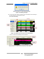
Step 1: After measuring the output of the 74HC164 chip, now is the time to
measure its input and observe the relationship between input and output.
74HC164 is a serial shifter chip, and it’s not a standard SPI chip, for the
convenience on observation, the 74HC164 chip that driving the LED is
controlled by the MCU through a SPI simulation interface. The P2.5 port of
P89LPC913 is output as the CLK (Clock) signal of SPI, and the P2.3 is output
as the DATO (data output) signal of SPI. When the CLK signal has a rising edge,
the data transmitting on DATO will start. The P0.6 port is the CS (Chip Select)
signal for SPI output, when this CS signal is low, there are data transmissions
on SPI. Connect these CS, CLK and DATO signals to the CH1, CH2 and CH3 of
the PODA respectively. Then select the [Setup]Æ[Bus/Signal] within the
software menu to open the setup window, add 3 new buses and named them
with CS, CLK, and DATO, as Figure 4-14 shows, then click the OK button.
Figure 4-14: Adding the SPI bus signals
z
Step 2: Click the run ( , run once) button within the software toolbar to start the
measurement of SPI input and the LED signals. After the measurement
completes, click the Full display (
results, as Figure 4-15 shows.
.
31
overall displaying) button to observe all
Please visit our Website:
www.embedtools.com
Chapter 4: Quick start tutorial
Figure 4-15: SPI transmission measurement result full displays
z
Step3: Zoom in the LED signal between 0xFE and 0xFD to observe the
relationship between SPI and LED signals, as Figure 4-16 shows
Figure 4-16: SPI transmission
From the measurement results we can find out how DATO outputs are
translated to LED control signals at the rising edge of the CLK signal.
.
32
Please visit our Website:
www.embedtools.com
Chapter 4: Quick start tutorial
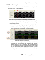
4.5 SPI data analysis
Generally, when we want to analyze the SPI transmission data, we need to compare
each rising edge of the CLK signal with the outputs manually; then calculate the data
value by counting bits. It’s definitely a boring job, are there any ways to simplify it?
The answer is YES; but with the LA2532 logic analyzer, we have a much quicker
way to perform this kind of jobs, that is, use the SPI Bus analysis plug-in provided
by LA2532.
z
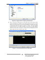
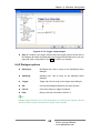
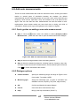
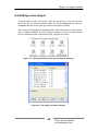
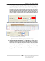
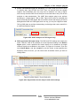
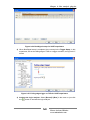
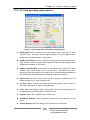
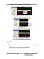
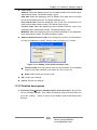
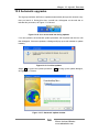
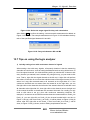
Step1: Select the [Tool]Æ[Plug-in Manager] to bring up the plug-in manager
dialogue, as Figure 4-17 shows.
Figure 4-17: The plug-in manager window
z
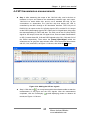
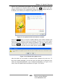
Step 2: Select the [SPI bus analysis] plug-in and click Setting… button to
bring up the SPI decoding setup dialogue. Then set “CLK” for Clock Signal
item, “CS” for SSEL (Chip Select) item, MSB for LSBF item, “8” for Frame
Length item, and “CPOL=0 CPHA=0” for SPI Mode item, clear the Enable
option of MOSI bus blank and tick the Enable option of MISO bus; then select
“DATO” in Source Signal of MISO, leave other setting to default; as Figure
4-18 shows.
.
33
Please visit our Website:
www.embedtools.com
Chapter 4: Quick start tutorial
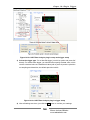
Figure 4-18: SPI analysis settings
z
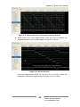
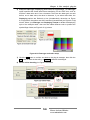
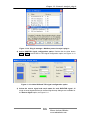
Step 3: click OK to confirm your setting and back to the plug-in manager, then
click OK again to confirm. Then, a bus named “OUT” will appear next to the
DATO bus, as the red box area in Figure 4-19 shows.
Figure 4-19: SPI data analysis result
The “OUT” bus presents the result of SPI transmission analysis; as the red box
area in Figure 4-19 shows, the data transferred on SPI bus is 0xFD, which is
exactly the same with the expected value at 74HC164, the analysis works as
intended. So with the analysis plug-ins, it’s very convenient for user to analyze
the data being transmitted on specific buses; it greatly simplifies the analysis
work for engineers since the plug-in handles most of the calculations in bitwise
based on protocol or bus specifications.
.
34
Please visit our Website:
www.embedtools.com
Chapter 4: Quick start tutorial
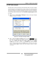
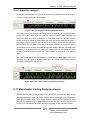
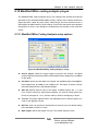
4.6 Trigger settings
Trigger is a useful tool that can help us focus to specific locations or segments of a
signal, such as disturbance, abnormal controls, and transmission errors. The logic
analyzer will start the recording when the trigger conditions are satisfied. Since the
sampling data is massive and increasing rapidly without stop (even faster when
using higher sampling frequency), but the recordable size of logic analyzer is limited,
so usually it’s not possible to record all sampled data. So, setting a good trigger
allows you to save your resources and focus more on interested fields; also allow
you to find out problems quickly and precisely. The following is the steps to setup a
trigger for the abovementioned SPI bus analysis example
z
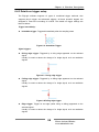
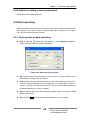
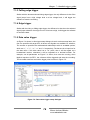
Step 1: Click the [Setup]Æ[Trigger…] to open the trigger setting window to
setup the trigger conditions. For this example, if we need to set a trigger at the
beginning of the SPI transmission, we can set a falling edge trigger, and use the
falling edge of CS as trigger conditions, as Figure 4-20 shows.
Figure 4-20: Setting a falling edge trigger
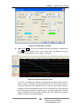
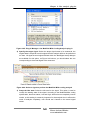
z
.
Step 2: Click the OK button, then click the Run ( , run once) icon within the
toolbar; then the measurement result displays, as Figure 4-21 shows.
35
Please visit our Website:
www.embedtools.com
Chapter 4: Quick start tutorial
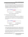
Figure 4-21: Result of falling edge trigger
The
mark within the figure shows that the position of trigger, as the figure
shows, the trigger point is at the falling edge of CS, which matched with the
settings.
Since the LA series Logic analyzer has the trigger position adjustment ability,
and the trigger position is using its default setting (10%), so the pre-trigger parts
of the signal is also visual for user. This trigger position adjustment ability allows
user to observe the data before and after the trigger, this function is very useful
for debugging. If a trigger is set to observe an error, the logic analyzer with the
trigger position adjustment ability can record the data before and after the
trigger, so that user can analyze the data and find out why this error occurred
and how the system handled it.
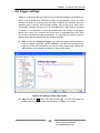
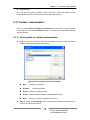
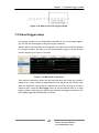
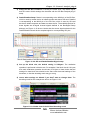
4.7 Plug-in trigger
Several types of LA series logic analyzers also have a plug-in trigger function.
Plug-in trigger is a trigger base on the result of a plug-in bus analyzer algorism. The
Trigger condition shown in Figure 4-21 is the falling edge of CS signal, and we found
that the transmitting data for this falling edge is 0xFD. So a question may come out:
can we use this 0xFD as a trigger condition, and only trigger when the SPI bus is
transmitting a 0xFD, and not trigger for other SPI data?
As Figure 4-22 shows, the SPI bus initiate multiple actions on CS, CLK, and DATO
signals to transfer a 0xFD value.
Figure 4-22: Transmitting 0xFD value on SPI bus
.
36
Please visit our Website:
www.embedtools.com
Chapter 4: Quick start tutorial
So, it is too complex to describe it with normal trigger types. But the LA series logic
analyzer can handle this by using its Plug-in trigger, which is a special function
designed for this kind of analysis.
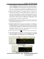
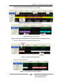
z
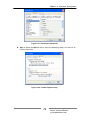
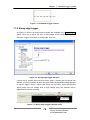
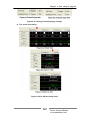
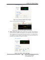
Step 1: Click the [Setup]Æ[Trigger…] to bring up the trigger setup dialogue,
then select SPI bus analysis option under the plug-in trigger to show its settings
on the right side of the dialogue; then fill in a “0xFD” in Data field, as Figure
4-23 shows.
Figure 4-23: Plug-in trigger configurations
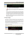
z
Step 2: Click the OK button to confirm the settings. Then click the Run ( , run
once) to start the sampling, the recording will start after the trigger condition
satisfied, Figure 4-24 shows the trigger result of this example.
Figure 4-24: Plug-in trigger result
In Figure 4-24 we can see that when SPI bus transmits a 0xFD value, the logic
analyzer is triggered and start the recording on data. This completely meets the
requirements.
.
37
Please visit our Website:
www.embedtools.com
Chapter 4: Quick start tutorial
The plug-in trigger is a characteristic of LA series logic analyzer, with this
function, use can quickly setup a complex trigger based on bus signals; it
greatly improves the development efficiency.
.
38
Please visit our Website:
www.embedtools.com
Chapter 5: Menu descriptions
Chapter 5: Menu descriptions
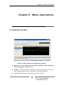
5.1 Operation window
Figure 5-1: Main interface of the application software
.
z
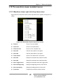
Menu bar: Contains [File], [Record], [Setup], [Analyze], [View], [Window],
[Tool], [Language] and [Help] options.
z
Toolbar: Contains the shortcut buttons for frequently used functions, such as
start, zooming, locate, search, configuration, and cursor operations.
z
Logic pen: Showing the current states of D0~D31 channel.
39
Please visit our Website:
www.embedtools.com
Chapter 5: Menu descriptions
z
Multi-document structure: Open multiple files at a same time.
z
Customized cursor: Display the cursor customization information.
z
Tree structure groups: Display a defined bus in tree structure groups.
z
Customize color and width: Customize the displaying color and set the
displaying width of the waveform for a bus signal.
z
Protocol analysis: Perform protocol analysis on a signal.
z
Hexadecimal display: Display the bus status in hexadecimal form.
z
Cursor pointing notes: Display the related information of the items where the
cursor is pointing to.
z
Status bar: Display the sample rate and working status of the logic analyzer.
z
Automatic measuring: Display the defined measurement value, which can be
set to the value of a specified interval between two markers, frequency, duty
ratio, or on-change calculations.
5.2 The File menu
Figure 5-2: The File menu
.
40
Please visit our Website:
www.embedtools.com
Chapter 5: Menu descriptions
z
New:
Create a new blank file.
z
Open:
Open a saved file.
z
Close:
Close current editing file.
z
Save:
Save current editing file to disk.
z
Save All:
Save all opened file to disk.
z
Save Backup as:
Save a copy of current file, the file name of the current
file will not change after saving it
z
Save as:
Save the current editing file in other name or format, the
name of the current editing file will change to the new
one after the saving action.
z
Export:
Export data from the current editing file and save it as a
binary file for reanalyze.
z
Export as CVS file:
Export data and save in CVS format, so that you may
use The Microsoft Excel to reanalyze the data.
z
Print:
Print out the current displayed screen.
z
Print Preview:
Preview the printing results on your PC.
z
Print Setup:
Setup the Printer.
z
E:\logic new\zlglog2: The recent files (multiple)
z
Exit:
Exit the zlglogic software.
5.3 The Record menu
Figure 5-3: The Record window
z
.
Run:
Activate the device, once the triggering conditions are
satisfied, the recording starts. The recording will stop
when the storage for the data is full, then the device is
deactivated.
41
Please visit our Website:
www.embedtools.com
Chapter 5: Menu descriptions
z
Run repetitive:
Activate the device, once the triggering conditions are
satisfied, the recording starts. The recording will pause
when the storage for the data is full, then it will continue
when the triggering conditions are satisfied again. These
actions will repeat till the Stop option within the sampling
menu is selected.
z
Stop:
Stop the recording and deactivate the device, and then
display the newly sampled data on the screen.
5.4 Setup menu
Figure 5-4: The Setup menu
z
Bus/Signal: Setting the Buses and Signals. User may divide the signals into
groups and then give each group a name. The group names of the bus will be
displayed in waveform views and trigger setups options, if you are not setting
this option, PodA0~PodA15 will be grouped into a default Bus named MyBus0,
PodA0 also belongs to a default Signal named MyBus1.
z
Sampling: Setting the sampling rate, threshold voltage, digital filtering, and
trigger positions.
z
Trigger:
Setting the triggering conditions, this may reduce the sampling on
useless data, and it supports up to 12 types of triggering conditions, such as
plug-in triggering, high level triggering and etc.
Tips:
LA2532 can combined multiple signal channel into one Bus, and any signal channel
can also be defined by different Buses and Signals
.
42
Please visit our Website:
www.embedtools.com
Chapter 5: Menu descriptions
5.5 The Analyser menu
Figure 5-5The analyze window
.
z
Go to Begin of Data:
Display the beginning section of the data.
z
Previous Page:
Display the contents on previous page.
z
Go to Trigger:
Display the triggering section of the data.
z
Next Page
Display the contents on next page.
z
Go to End of Data:
Display the ending section of the data.
z
Find:
Search a specific data within the current active file.
z
Find Previous:
Search the previous specific data within the current
active file.
z
Find Next:
Search the next specific data within the current
active file.
z
Add Markers:
Add a marker within the waveform window. User
can name it and set up its color.
z
Go to Markers:
Display the data section near the marker.
z
New Measurement:
Add new Measurement information between two
markers to the measurement information bar.
43
Please visit our Website:
www.embedtools.com
Chapter 5: Menu descriptions
5.6 The View Menu
Figure 5-6: The View Option
z
Tool Bar:
Show/Hide tool bar, including standard, logic pen,
markers, and Customization options.
z
Status Bar:
Show/Hide status bar.
z
Auto measure window:
Show/Hide auto measure window.
z
Show Horizontal Lines: Show/Hide horizontal lines.
z
Show Vertical Lines:
Show/Hide vertical lines.
z
GUI Style:
Define the style of GUI (Graphic User Interface),
including the Office 2000, Office XP, Office 2003 and
Window XP.
z
Zoom In
Zoom in the waveform views.
z
Zoom Out
Zoom out the waveform views
z
Zoom Out Full
Zoom out for a full view of the waveform.
5.7 The Window menu
Figure 5-7: The Window menu
.
44
Please visit our Website:
www.embedtools.com
Chapter 5: Menu descriptions
z
Cascade:
Cascade the opened windows.
z
Tile:
Tile the opened windows.
z
ZLglog1:
The current opened window of this example
5.8 The Tool Menu
Figure 5-8: The Tool Menu
z
Note pad:
Open the note pad window
z
Calculator:
Open the calculator window
z
Paint:
Open the painting window
z
Plug-in manager:
Open the plug-in manager
5.9 The Language menu
Figure 5-9: The Language menu
.
z
Chinese:
View in Chinese
z
English:
View in English
45
Please visit our Website:
www.embedtools.com
Chapter 5: Menu descriptions
5.10 The Help menu
Figure 5-10: The Help menu
z
Help topic:
View the online helping file.
z
Updates:
Check for updates.
z
About zlgLogic: Information about the zlgLogic software.
5.11 The Toolbar customization menu
Move your cursor to the Tool menu within the menu bar, then it will show up its
submenus, as Figure 5-11 shows, within this menu, you may view/hide the standard
toolbar, Logic pen tool and Cymometer tool, so that you can select “Customize” to
customize the tool bar components, detail about this will be described in the
introductions to user toolbar customize window.
Figure 5-11: The submenu of Tool bar
.
46
Please visit our Website:
www.embedtools.com
Chapter 5: Menu descriptions
5.12 The waveform viewer assistant menus
5.12.1 Waveform viewer right click drop down menu
Right click on the waveform viewer, then a drop down menu appears, as Figure 5-12
shows.
Figure 5-12: Drop down menu for waveform recorder
.
z
Zoom In:
Zoom in for more details
z
Zoom Out:
Zoom out for observations
z
Zoom Out Full:
Zoom out for a complete view
z
Place M1:
Place the M1 marker on this place
z
Place M2:
Place the M2 marker on this place
z
Insert marker:
Insert a new marker with a new name
z
Go to M1:
Display the contents around the M1 marker
z
Go to M2:
Display the contents around the M2 marker
z
Go to Trigger Point:
Display the contents around the Trigger point
z
Go to the beginning:
Display the beginning section of the record
z
Go to the ending:
Display the ending section of the record
z
Properties:
Configure the waveform viewer window
47
Please visit our Website:
www.embedtools.com
Chapter 5: Menu descriptions
5.12.2 Waveform selection drop down menu
From left to right, hold you left mouse key to drag a box and select a segment of
waveform; when you release your mouse key, a menu will then appear to ask you
how to handle this section of waveform.
Figure 5-13: Waveform selection drop down menu
z
Zoom In:
Zoom in to view the details of this area
z
Set Trigger:
Set the selected waveform segment as a trigger
z
Find Next:
Find next similar area
z
Find Previous:
Find previous similar area
z
Save to BMP:
Save the selected waveform segment to BMP image file.
z
Save to Clipboard:
Copy the selected waveform segment to clipboard
5.13 Waveform files and Bus/Signal assistant menus
5.13.1 Waveform file right click drop down menu
Right click on the file name on top of the waveform viewer to bring up a drop down
menu, as Figure 5-14 shows.
.
48
Please visit our Website:
www.embedtools.com
Chapter 5: Menu descriptions
Figure 5-14: File operation drop down menu
z
Close:
Close the file
z
Save:
Save the file
z
Save Backup as:
Save a backup with different name
z
Export:
Export the data portion of the file for secondary analysis
z
Export as CSV file:
Export the data portion of the file to CSV format file that
can be edited by Microsoft Excel.
5.13.2 Bus/Signal right click drop down menu
Right click on the bus/signal name on the left side of the waveform viewer, such as
MyBus0, a drop down menu will appear, as Figure 5-15 shows.
Figure 5-15: Bus/Signal drop down menu
.
z
Insert Before:
Add a bus/signal before the selected bus/signal
z
Insert After:
Add a bus/signal after the selected bus/signal
z
Delete:
Delete the selected bus/signal
z
Properties:
Configure the selected bus/signal
49
Please visit our Website:
www.embedtools.com
Chapter 6: Function Descriptions
Chapter 6: Function Descriptions
6.1 Bus/Signal Setups
The sampling and recording actions of the LA series logic analyzer can only be
performed on those existing signals or buses. So, in order to perform these actions,
user should define the signals or buses for the sampling channels first. And this can
be done in the Bus/Signal setup dialogue.
6.1.1 Quick guide on bus/signal setup
z
Step 1: click the shortcut button
or select the [Setup]Æ[Bus/Signal] option
within the menu bar to bring up the Bus/Signal Setup dialogue, as Figure 6-1
shows
Figure 6-1: Bus/Signal Setup dialogue
.
50
Please visit our Website:
www.embedtools.com
Chapter 6: Function Descriptions
z
Step 2: Delete the default bus and signal and add your new signals or buses
Delete a bus/signal: left click to select the bus/signal you want to delete.
Press Delete button to delete it.
z
Add a bus/signal: left click on the Insert button to insert a new bus/signal,
left click on the default name MyBus0 of the new signal/bus to change it.
Then tick the channel you want to sample within its channel list.
Step 3: Use the Up and Down button to change the displaying order of a Bus or
signal. Then click OK to confirm your settings.
Tips:
You can also configure the sampling ratio and trigger within the setup window, just
select their corresponding clip to bring up their setup interface
6.1.2 Dialogue Options
.
z
Bus/Signal:
Bus/Signal clip, click to enter the Bus/Signal parameter
setup window
z
Sampling:
Sampling clip, click to enter the sampling parameter
setup window
z
Trigger:
Trigger clip, click to enter the trigger setup window
z
Name:
The name of the bus/signal
z
Bits:
The bit length of the corresponding signal/bus
z
Pod B:
Corresponding to all brown probes of the logic analyzer
z
Pod A:
Corresponding to all grey probes of the logic analyzer
z
Insert:
Insert a new bus/signal
z
Delete:
Delete a selected bus/signal
z
Up:
Move the selected bus/signal up one place
z
Down:
Move the selected bus/signal down one place
z
OK:
Confirm your modifications on bus/signal setups
z
Cancel:
Cancel your modifications on Bus/Signal setups
z
Help:
Get help from the software (Press F1 also works)
51
Please visit our Website:
www.embedtools.com
Chapter 6: Function Descriptions
6.1.3 Details on setting a Bus/Signal
1) Add a new Bus/Signal or change the name of an existing bus/signal
User can use the Insert button to add a new Bus/Signal; also can click the name of
an existing Bus/Signal to change it.
Notes: Use only these characters to specify you bus/signal name: ‘0’~’9’, ‘A’~’Z’, ‘a’~’z’,
spacebar and ‘_’ (underline)
2) Assign Sampling channels for a bus/signal
After clicking the Insert button to create a new bus or signal, you may then assign
the channels that required for sampling; just tick it/them after the signal/bus name.
For a single channel sampling, we call it a signal; for multiple channel sampling, we
call it a bus. Please make sure the assigned channels are corresponding to the
required probes.
Tips:
For buses with continuous channel bits (which means that the check boxes for each
sampling channel are continuous on the Bus/Signal setup dialogue), you can just
right click to tick all bits quickly. Right click on a bit will reverse its state, and all bits
after it will be changed to the same state with this bit.
For example, in Figure 6-1, if you want to measure bit A15~A8 of Pod A in MyBus0,
you can just right click the A15, then all bits are ticked, after this, right click on A7,
then A0~A7 will be clear so that only A15~A8 remain ticked. So actually you only
need to click twice for setting a continuous 8 bits.
3) Change the list order of a Bus/Signal
Select the signal you want to move, click “Up” or “Down” button to change its
displaying order in the list.
4) Delete a Bus/Signal
Select the unwanted Bus/Signal, click Delete to remove it from the list.
5) Confirm the settings
Just click “OK” to confirm your settings when you finish setting the Bus/Signal;
otherwise, click “Cancel” to discard the changes.
6.2 Setup Bus/Signal properties
The properties of a Bus/Signal include the name, color, and the corresponding
channel(s), all these can be configured within the Bus/Signal properties window.
.
52
Please visit our Website:
www.embedtools.com
Chapter 6: Function Descriptions
6.2.1 Quick guide on bus/signal properties setup
z
Step 1: Right click on any bus or signal within the bus/signal dialogue to bring
up the context-sensitive menu, then click “properties” to pop up the bus/signal
properties dialogue, as Figure 6-2 shows.
Figure 6-2: Bus/Signal Properties dialogue
z
z
Step 2: modify the properties of the bus or signal
Name: Enter a new name for this bus or signal
Color:
Select channels: Just tick the channel you want to record
Click to select the displaying color for this bus/signal.
Step 3: Click OK to confirm and dismiss the dialogue.
6.2.2 Dialogue options
.
z
Name:
User can change the bus/signal name here.
z
Color:
Click to select a displaying color for this bus/signal.
z
Pod A:
Corresponding to all grey probes of the logic analyzer;
tick it to activate the measuring on this probe.
z
Pod B:
Corresponding to all brown probes of the logic analyzer;
tick it to activate the measuring on this probe.
z
GND:
The black probe of the logic analyzer is system ground.
z
NC:
The orange probes are reserved ports
z
OK:
Confirm the settings and dismiss the dialogue.
z
Cancel:
Cancel the settings and dismiss the dialogue.
53
Please visit our Website:
www.embedtools.com
Chapter 6: Function Descriptions
6.2.3 Details on sampling setups
1)
Add/change the name of a Bus/Signal
Fill in or modify the bus/signal name in the Name field, such as “MyBus0”
Notes: Use only these characters to specify you bus/signal name: ‘0’~’9’, ‘A’~’Z’, ‘a’~’z’,
spacebar and ‘_’ (underline)
2)
Assign Dx bits for the bus/signal
Just tick the Dx bit you want to record, or clear the Dx bits you don’t want to record.
Notes: For continuous bits, you can right click on bits to set them quickly; a right click on a bit can
reverse its state and also affects all bits after this bit and set them to the same state.
3)
Set Bus/Signal displaying color
Click the color menu within Figure 6-3 to open dialogue for color selection, as Figure
6-3 shows. Click to select your favorite color, and click OK to confirm your
bus/signal properties settings.
Figure 6-3: Bus/Signal properties color selection menu
6.3 Sampling setup
Before sampling, correctly setting the sampling frequency, threshold voltage and
other sampling parameters are very important for getting a precisely waveform.
.
54
Please visit our Website:
www.embedtools.com
Chapter 6: Function Descriptions
6.3.1 Quick guide on sampling setups
z
Step 1: click the
button within the toolbar or select [Setup]Æ[Sampling…]
option within the menu bar to bring up the sampling setup dialogue, as Figure
6-4 shows.
Figure 6-4: Sampling setup
z
Step 2: Set up the sampling frequency. The default setting is 100MHz, this
frequency can satisfy most situations. Lower frequency may have longer record
time. Left click on OK can confirm the settings and dismiss this dialogue.
6.3.2 Dialogue Options
.
z
Bus/Signal:
The Bus/Signal clip, single click on it to bring up the
Bus/Signal setup dialogue.
z
Sampling:
Sampling clip, click it to bring up the Sampling setup
dialogue.
z
Trigger:
Trigger clip, click it to bring up the trigger setup dialogue
z
Frequency:
Set your sampling frequency here, you can fill in a
specific value within this item and select the unit of
frequency as Hz, KHz or MHz
55
Please visit our Website:
www.embedtools.com
Chapter 6: Function Descriptions
z
Threshold Setting:
Set the signal threshold voltage.
You can select a value within 7 available options:
LVCMOS (1.7V), LVTTL (2.00V), 1.5V I/O (0.98v), 1.8v
I/O (1.17V), 2.5V I/O (1.70V), 3.3V PCI (1.65V), 5V PCI
(2.00V); or you can fill in a value between 0V and 4.6V.
z
Digital filter:
Three options are available here: None, 1 or 2. The
filtering is run in hardware; select none to deactivate this
function, select “1” means a 2 of 3 filtering, select “2”
means a 3.of 5 filtering.
z
Acquisition:
Select the capacity of a record.
z
Compress:
Enable/Disable
acquired data.
z
Trigger position:
This is the percentage of the pre-trigger data comparing
to the total recorded data.
z
Save to file when sampling repetitively: Tick this option to save the record
file on every time the sampling cycle repeats.
z
OK:
Confirm and dismiss the dialogue
z
Cancel:
Pop up the help information (Press F1)
the
real-time
compression
to
the
6.3.3 Details on sampling setups
1) Specify the sampling frequency
User can select or just fill in a frequency within the Frequency field, and the unit of
the frequency can be set to Hz, KHz, or MHz.
Notes: The inputted frequency should be limited between 0~100MHz. The inputted frequency
should be a divisor number of 100M, if it’s not, when you switch to other options, the software
will find a nearest number to replace your setting.
2) Specify the threshold voltage
There are 7 available options, user can select one for each signal of D15~D0 and
D31~D16; or just specify a voltage value between 0 and 4.6 V.
3) Acquisition capacity selection
User can select different storage capacities of a record for the logic analyzer,
available options are 1K, 2K, 4K, 8K, 16K, and 32K sampling points; the default
setting is 32K sampling points.
.
56
Please visit our Website:
www.embedtools.com
Chapter 6: Function Descriptions
4) Compress
Tick it to enable the real-time data compression. This option is useful for long period
measurements, allowing the logic analyzer to record more data under the same
storage capacity.
Tips:
Enable is recommended.
5) Digital filter selection
Three options are available: None, 1 or 2. The filtering is run in hardware, select
None to disable this function, select “1” means a 1 sampling clock pulse filtering,
select “2” means a 2 sampling clock pulse filtering.
Tips:
When there are many clutters on the sampling waveform, analysis result may have
errors. For this situation, you can try to change the threshold voltage or set a digital
filter to solve the problem. If you select None within the digital filter option, the filter
will be deactivated, if you select filter 1, it will filter the non-continuous pluses that
lasts one sampling clock; if you select filter 2 it will filter the non-continuous pluses
that lasts less than two sampling clocks.
6) Trigger position
This option sets how much pre-trigger data can be recorded and displayed
7) Save to file when sampling repetitively
Tick this option to save each trigger wave form to a file in repetitive running mode;
the file name will be saved like:
“CurrentFileName_0.zla”, “CurrentFileName_1.zla”…“CurrentFileName_n.zla”.
6.4 Trigger setup
A logic analyzer can not only be set to trigger at the startup, but also it can be set to
trigger at different conditions. Through the operation listed below, you can set up
your trigger mode quickly and precisely.
6.4.1 Quick guides on trigger setup
z
.
Step 1: click on the
button or select the [Setup]Æ[Trigger…] option within
the menu bar to open the trigger setup dialogue, as Figure 6-5 shows.
57
Please visit our Website:
www.embedtools.com
Chapter 6: Function Descriptions
Figure 6-5: The Trigger setup dialogue
z
Step 2: Configure your trigger method, select the trigger type on the left side of
the dialogue and then the parameters of this trigger method will show up on the
right side. After configurations, click OK to confirm your settings.
6.4.2 Dialogue options
z
Bus/signal:
Bus/Signal clip, click to bring up the Bus/Signal setup
dialogue
z
Sampling:
Sampling clip, click to bring up the Sampling setup
dialogue
z
Trigger:
Trigger clip, click to bring up the trigger setup dialogue
z
OK:
Confirm the settings and dismiss the setup window
z
Cancel:
Cancel the setting on trigger conditions
z
Help:
Bring up the help information (Press F1)
Tips:
Multiple trigger method is one of the advantages of LA series logic analyzer. We will
spread a whole chapter to describe the trigger setup in details.
.
58
Please visit our Website:
www.embedtools.com
Chapter 6: Function Descriptions
6.4.3 Details on trigger setup
The ZlgLogic software supports 12 types of conditional trigger methods, also
supports plug-in trigger and advanced triggers, all these powerful triggers are
designed to control the recording of LA2532. The details on trigger settings are
listed as below:
Trigger immediately:
z
Immediate trigger: Triggered immediately after the sampling starts
Figure 6-6: Immediate Trigger
Signal triggers:
z
Rising edge trigger: Triggered by a rising edge appeared on the selected
signal.
Usually it’s used to detect the change of a single signal, such as read/write
signals.
Figure 6-7: Rising edge trigger
z
Falling edge trigger: Triggered by a falling edge appeared on the selected
signal.
Usually it’s used to detect the change of a single signal, such as read/write
signals.
Figure 6-8Falling edge trigger
z
.
Edge trigger: Trigger for an edge (either rising or falling) appeared on the
selected signal.
Usually it’s used to detect the change of a single signal, such as read/write
signals.
59
Please visit our Website:
www.embedtools.com
Chapter 6: Function Descriptions
Figure 6-9: Edge trigger
Bus triggers
z
Data value trigger: Trigger at the appearance of a specified value on the
selected bus. If the inputted value has a prefix “0x”, it will be treated as a
hexadecimal number, otherwise it will be treated as a decimal number.
Usually it’s used to detect specific data values, such as output data status.
Figure 6-10: Data value trigger
z
Data queue trigger: Triggered by a data queue that appeared sequentially on
the selected bus (pattern). If the inputted value has a prefix “0x”, it will be
treated as a hexadecimal number, otherwise it will be treated as a decimal
number.
Usually it’s used to capture a bus operation, such as communication protocol
signs.
Figure 6-11: Data queue trigger
Synthesis triggers
z
.
Data value and rising edge trigger: Triggered by a specified value appeared
on the selected bus and a rising edge appeared on the selected signal. If the
inputted value has a prefix “0x”, it will be treated as a hexadecimal number,
otherwise it will be treated as a decimal number.
Usually it’s used to detect a certain data value, such as the read/write access to
a specific address
60
Please visit our Website:
www.embedtools.com
Chapter 6: Function Descriptions
Figure 6-12: Data value and rising edge trigger
z
Data value and falling edge trigger: Triggered by a specified value appeared
on the selected bus and a falling edge appeared on the selected signal. If the
inputted value has a prefix “0x”, it will be treated as a hexadecimal number,
otherwise it will be treated as a decimal number.
Usually it’s used to detect certain types of operations, such as the read/write
access to a specified address.
Figure 6-13: Data value and falling edge trigger
Time related triggers
z
Lasting duration trigger: Triggered if a specified value appeared on the
selected bus and then lasted over a specified duration.
Usually it’s used to detect abnormal situations, such as the width error of PWM
output and burr analysis.
Figure 6-14: Lasting duration trigger
z
Data arrival and delay trigger: Triggered at the expiration of the specified
delay period started from the appearance of a specified data value on the
selected bus
The unit of the time for the delay is calculated by sampling rates, for example, if
the sampling frequency is 100MHz, then the unit of the time is 10ns
Figure 6-15: Data arrival and delay trigger
.
61
Please visit our Website:
www.embedtools.com
Chapter 6: Function Descriptions
z
Data passed and delay trigger: Triggered at the expiration of the specified
delay period started from the changed (end of lasting) of the specified value on
the selected bus.
The time unit is one sampling period For example, if the sampling frequency is
100MHz, then the time unit is 10ns.
Figure 6-16: Data passed and delay trigger
Occurrence counting trigger
z
Occurrence counting trigger: Trigger by the occurrence counting of a
specified value on the selected bus (pattern). If the inputted value has a prefix
“0x”, it will be treated as a hexadecimal number, otherwise it will be treated as a
decimal number.
Usually it’s used to find out specific error conditions, such as program error
outputs.
Figure 6-17: Occurrence counting trigger
Plug-in triggers
z
I2C Bus analysis Trigger
z
1-Wire Bus Analysis Trigger
z
SPI Bus Analysis Trigger
z
SSI Bus Analysis Trigger
z
Serial UART Bus Analysis Trigger
Advanced Triggers
z
.
Advance Triggers: This trigger mode is combined by a sequence of steps;
each step has three parts: conditions, operations to perform when conditions
are satisfied, and the operations to perform when conditions are not satisfied.
62
Please visit our Website:
www.embedtools.com
Chapter 6: Function Descriptions
6.5 Run and Stop
When the sampling frequency, threshold voltage, trigger position and other settings
are all completed, you can start the running of your logic analyzer to record and
observe the signal waveforms. You can find a [Run ] and [Run Repetitive ]
options within the [Record] menu. Click either one of these options to start the
recording, as Figure 6-18 shows. Also there are two shortcuts within the tool bar can
do the same thing.
Figure 6-18: Run and stop
If you need to keep on recording without stop like an oscilloscope, you should start it
by clicking the “Run Repetitive” option. This command will start the recording of
data repetitively, it will not stop after the first trigger-record-display procedure, and it
just repeats this procedure until you stop it.
6.6 Add markers
The markers on the waveform viewer window can be used to mark and measure the
acquired data. The default markers are T, M1 and M2. Marker T represents the
trigger position. You can add new markers if you wanted, they can simplify your
analysis works by marking out importance places of the signal.
6.6.1 Quick guides on adding a new marker
z
.
Step 1: Click the
button within the tool bar or select [Analyser]Æ[New
marker…] option to bring up the new marker dialogue, as Figure 6-19 shows.
63
Please visit our Website:
www.embedtools.com
Chapter 6: Function Descriptions
Figure 6-19: The new marker dialogue
z
Step 2: Enter the new marker name and select the displaying color for it by
clicking the small arrow on the right-bottom of the color cell.
z
Step 3: Select a position to put the new marker (three available options, centre
of the waveform viewer screen, specific time, or specific sampling point). Then
click OK to confirm and dismiss the dialogue.
6.6.2 Dialogue options
z
Name:
Enter the new marker name here
z
Color:
Select a color for the new marker by within the drop
down menu
z
Position:
The position to put the new marker, three options are
available: centre of the waveform viewer screen, preset
time, preset sampling point
z
OK:
Confirm the settings and dismiss the dialogue
z
Cancel:
Do not add a new mark and dismiss the dialogue
6.6.3 Details on adding a new marker
1) Name
You can specify a name for the new marker and this name will be display on top of
the marker.
2) Color
Click the color cell to open its drop down menu, as Figure 6-20 shows, click to select
one new color for the marker, this helps to distinguish different markers.
.
64
Please visit our Website:
www.embedtools.com
Chapter 6: Function Descriptions
Figure 6-20: Color selection for the new marker
3) Place
Set a position to place your new marker, you can select centre of screen, time, or
sample point. The default setting is the centre of the waveform viewer screen. If you
want to place it based on time or sampling points, you can tick the option and then
fill in the time or sampling point value where the marker should be placed.
6.7 Finding markers
After sampling the signal, zooming in or moving the viewer screen could make a
marker out of the displaying area. How to find a marker quickly? You can use the
marker finder dialogue.
6.7.1 Quick guides on finding markers
z
Step 1: Click the
button within the tool bar or select [Analyser]Æ[Go to
marker] option to bring up the marker finder dialogue
Figure 6-21: The marker finder dialogue
.
65
Please visit our Website:
www.embedtools.com
Chapter 6: Function Descriptions
z
Step 2: Within the marker finder dialogue, it will list out all markers with names
and positions (including the new markers defined by user), click the marker you
want to view and then click OK to shift screen center of the waveform viewer to
the position of selected marker.
6.7.2 Dialogue options
z
Name:
List out all available markers
z
Position:
The position of the marker
z
OK:
Click to locate the selected marker
z
Help:
bring up the help information (Press F1)
6.7.3 Details on finding a marker
1)
Name:
list out all available markers, including new markers that defined by user, for
example, if you defined a new marker LABEL, then it should be on the list, as
Figure 6-21 shows.
2)
Position:
The positions of the markers are displayed in sampling points; for example if M1
was placed at the 40th sampling points, if the sampling frequency is different,
then the sampling time of it is different. For example, in Figure 6-22 the
sampling frequency is 100MHz, so the time period for each sampling point is
10ns.
Figure 6-22: Sampling setting dialogue
.
66
Please visit our Website:
www.embedtools.com
Chapter 6: Function Descriptions
6.8 Add auto measurements
There is an auto measurement bar under the waveform viewer, showing the instant
results on several types of calculation between two markers, the default
measurements are time intervals between M1 and M2, which will be (M1-M2) and
frequency, which will be 1/(M1-M2) if they are located at one cycle period of the
signal. User can also add new auto measurements into this bar based on their
requirements; these instant results can save their time on doing such kind of
calculations, allowing user to get a first glimpse on the aspect of signals.
6.8.1 Quick guides on adding a new auto measurement
z
Step 1: Click the
button within the toolbar or select [Analyser]Æ[New
Measurement…] within the menu bar to open the add measurement dialogue.
Figure 6-23: Add new measurements dialogue box
z
Step 2: Select two target markers from the existing markers.
z
Step 3: Select the measuring objective, including interval, frequency, duty ratio,
and edge counter four kinds of measurements, and the default option is interval.
Click OK to confirm and dismiss the window.
6.8.2 Dialogue options
.
z
Choose markers:
Specify the measuring range, the range in Figure 6-23 is
from marker T to marker LABEL
z
Measuring type:
Setup the measuring type, (4 types of calculation are
available: interval, frequency, duty ratio, edge counter)
z
OK:
Confirm and dismiss the setup dialogue
z
Cancel:
Cancel this auto measurement setup
z
Help:
Bring up the help information (Press F1)
67
Please visit our Website:
www.embedtools.com
Chapter 6: Function Descriptions
6.8.3 Details on adding a new measurement
Please refer to Auto Measurements
6.9 Data searching
After the recording, the waveform viewer window may have complex waveforms and
many signals. If you want to search a specific data within a specific bus or signal,
you can use the data searching function.
6.9.1 Quick guides on data searching
z
Step 1: Click the
button within the toolbar or select [Analyser]Æ[Find…]
option to bring up the data searching dialogue.
Figure 6-24: Data searching dialogue
.
z
Step 2: Enter the bus/signal name you want to search, and the location to start
the searching, usually it will be a marker.
z
Step 3: Specify the data values you want to search, the searching range can be
a set to included, excluded, equal (=), bigger than (>), smaller than (<), and not
equal (!=); just fill in the values to specify it. You can select different searching
methods depending on what you needed.
z
Step 4: Specify the action after searching; default action is to places a Find
marker on the result.
z
Step 5: Click Next to find another match data based on your settings
68
Please visit our Website:
www.embedtools.com
Chapter 6: Function Descriptions
6.9.2 Dialogue options
z
Bus/Signal Name:
The bus signal name to search
z
Start from:
The starting position of the search
z
Search:
The conditions of the search
z
Min:
This option only available for buses, it specifies the
minimum value of the finding target, or the starting value
of a range
z
Max:
This option only available for buses, it specifies the
maximum value of the finding target, or the ending value
of a range
z
When find:
Specify the actions after finding out the result, such as
place marker M1, M2, or a new marker named Find.
z
Previous:
Find the previous point that satisfies the conditions.
z
Next:
Find the next point that satisfies the conditions.
z
Exit:
Exit the finding and dismiss the dialogue.
z
Help:
Bring up the help information (Press F1).
6.9.3 Details on data searching
1)
Bus/Signal name:
Click to bring up the drop down menu, find your target bus or signal within the
Bus/Signal name list, all default and new buses or signals are listed here.
2)
Start from:
Click to bring up the drop down menu and select an option form:
.
z
The beginning of data:
Start the searching from the beginning of the data
z
The end of data:
Start the searching from the end of last data record.
z
Current position:
Start the searching from current viewing area
z
Trigger point:
Start the searching from the trigger point
z
M1:
Start the searching from M1 marker
z
M2:
Start the searching from M2 marker
z
Previous:
The previous point that satisfied the conditions
z
Next:
The next point that satisfied the conditions
69
Please visit our Website:
www.embedtools.com
Chapter 6: Function Descriptions
z
X---:
3)
Find:
Start the searching from a user defined marker
Click to bring up the drop down menu and select a option:
z
When searching a signal, you can choose rising edge, falling edge, high voltage
level, low voltage level
z
When searching a bus, you can choose the included, excluded, equal to, bigger
than, smaller than, and not equal to option; also you should specify the
minimum value (or starting value) and the maximum value (or ending value) to
the data range derived from a bus
4)
Minimum value:
Only available to buses, the starting value of a range in a bus.
5)
Maximum value:
Only available to buses, the ending value of a range in a bus
6)
When found:
When a result is found, depending on this option, the software will put the M1/M2 or
user defined marker to the position where the result was found. Or just put a new
marker on the result position, user also can specify the new marker’s name, the
default name is Find.
7)
Finding direction:
User can click the Previous or Next button to search in different directions
6.10 Waveform viewer setups
The waveform viewer is the major window for observations and analysis. The
configurations on background color, grid color; and the displaying of vertical or
horizontal lines can assist the observing and analyzing of the waveforms.
6.10.1 Quick guides on waveform viewer setups
z
.
Step 1: Right click within the waveform viewer to bring up the context sensitive
menu, select the last option, Properties, to enter the waveform viewer
properties window.
70
Please visit our Website:
www.embedtools.com
Chapter 6: Function Descriptions
Figure 6-25: Waveform viewer properties dialogue
z
Step 2: Following the notice within the dialogue, modify the options you want to
change; then click OK to confirm and apply.
6.10.2 Dialogue options
z
Background color:
Setup the background color of the waveform viewer
window.
z
Grid color:
Setup the grid color of the waveform viewer window
z
Horizontal lines:
Display horizontal lines on the waveform viewer.
z
Vertical lines:
Display vertical lines on the waveform viewer.
z
OK:
Confirm the setting and dismiss the dialogue.
z
Cancel:
Cancel the setting and dismiss the dialogue.
6.10.3 Details on setting the waveform viewer
1)
Background color:
User can define the background color of the waveform viewer window by setting this
option.
2)
Grid color:
The horizontal lines and the vertical lines form up the grids, this option specifies their
color.
3)
Horizontal lines:
User can tick this option to display horizontal lines only, if both this option and the
vertical lines option are ticked, they will be displayed together.
.
71
Please visit our Website:
www.embedtools.com
Chapter 6: Function Descriptions
4)
Vertical lines:
User can tick this option to display vertical lines only, if both this option and the
horizontal lines option are ticked, they will be displayed together.
6.11 Toolbar customization
User can select [View]Æ[Toolbar]Æ[Customize] form the menu, or just right click
on the tool bar and select Customize option to customize the toolbar with different
shortcut buttons.
6.11.1 Quick guide on toolbar customization
z
Step 1: User can just tick or clear the list options to show or hide the related
toolbars or features, as Figure 6-26 shows.
Figure 6-26: Customizes bars and functions
z
.
Create a new toolbar
New:
Rename:
Delete: Delete an existing toolbar
Reset: Reset to default toolbar settings before change
Help:
Rename a toolbar
Bring up the help information (Press F1)
Step 2: Select the Commands clip to configure the shortcuts commands for a
tool bar, as Figure 6-27 shows
72
Please visit our Website:
www.embedtools.com
Chapter 6: Function Descriptions
Figure 6-27: Customize commands
z
Step 3: Select the Options clip to setup the displaying options for tool bar, as
Figure 6-28 shows.
Figure 6-28: Toolbar options setup
.
73
Please visit our Website:
www.embedtools.com
Chapter 7: Detailed trigger guides
Chapter 7: Detailed trigger guides
The major purpose of triggers for a logic analyzer is to record and analyze the useful
sections within massive data, help user to locate their concerning waveforms and
improve the efficiency on development and learning. Using a logic analyzer and with
the assistance of trigger, user can just set the error state as a condition, then the
analyzer will start and record the error whenever it happens even in a massive of
data, this function greatly improve the efficiency on verifications and debugging.
LA series Logic analyzer provides following powerful triggers:
12 fast trigger types
Visual triggers
Plug-in triggers
Advanced triggers
All these triggers make it become a powerful tool on handling difficult situations and
finding even the slightest errors on massive data flows.
7.1 12 types of fast triggers
7.1.1 Trigger Immediately
This trigger is set to start the recording once user presses the run button to start the
recording. When the data buffer is full it will stop recording and display the recorded
data on screen. Usually this trigger is used to observe the bus status.
Figure 7-1 shows how this trigger works; the red T within it indicates the trigger point,
and the square box area indicates the record buffer zone. The recording starts from
the beginning and ends at the place where the buffer fills; then the buffer data will be
displayed.
.
74
Please visit our Website:
www.embedtools.com
Chapter 7: Detailed trigger guides
Figure 7-1: Immediate trigger schema
7.1.2 Rising edge trigger
As Figure 7-2 shows, all single channel signals are available in the Target Signal
option, since only a signal can have a rising edge; a bus contains two or more
channels of signal, so there’s no “rising edge” for a bus.
Figure 7-2: Rising edge trigger dialogue
If there are no options within the drop down menu, it means that no signals are
defined, so user must define at least one signal within the Signal/Bus setup dialogue
to use this trigger. Select a signal, then press the run button; when the selected
signal jumps from low voltage level to high voltage level, the software will be
triggered and start the recording.
Figure 7-3: Rising edge trigger example result
.
75
Please visit our Website:
www.embedtools.com
Chapter 7: Detailed trigger guides
7.1.3 Falling edge trigger
Similar with the abovementioned rising edge trigger, the only difference is that if the
signal jumps form a high voltage level to a low voltage level, it will trigger the
software to start the recording
7.1.4 Edge trigger
Similar with the rising or falling edge trigger, the difference is that when the selected
signal jumps whatever form high to low or form low to high, it will trigger the software
to record the data.
7.1.5 Data value trigger
As Figure 7-4 shows, in this trigger setup dialogue, there’s are three setup items, the
first one specifies the target bus, all buses and signals are available for selection;
The second on specifies the mathematical relationships with six available options,
which are “>”, “<” “=”, “<=”, “>=” and “!=” respectively. The last one is an input box for
the data value. If the data value has a “0x” prefix, then it will be regard as a
hexadecimal number, otherwise it will be regarded as a decimal number. For
example, set all parameters as Figure 7-4 shows, then start the running; when
MyBus0 equals to 0xFFFC, the software will be triggered and start the recording.
The recorded waveform around the trigger point is shown in Figure 7-5.
Figure 7-4: Data value trigger setup dialogue
.
76
Please visit our Website:
www.embedtools.com
Chapter 7: Detailed trigger guides
Figure 7-5: Recorded Results of the example data value trigger
7.1.6 Data queue trigger
Figure 7-6: Data queue trigger setup dialogue
As Figure 7-6 shows, on the trigger setup dialogue there is an Add button. This
button is used to add new data values; every time user press it, it will generate a
new input box, allowing user to add data value in the queue. User can specify up to
8 data values; and sequentially they will form up a data queue; if this data queue
appears on the selected bus, the software will be triggered to record the sampling
data.
The data queue trigger is often used to capture some specific operations, such as
finding a sign of a communication protocol. Figure 7-7 shows an example trigger
seeking for data queue “123”, and contents within the box will be display on screen.
.
77
Please visit our Website:
www.embedtools.com
Chapter 7: Detailed trigger guides
Figure 7-7: Data queue trigger schema
7.1.7 Data value and rising edge trigger
This type of trigger is a combination of data value trigger and rising edge trigger. As
its name describes, the software will only triggered when both conditions are
satisfied. Usually this trigger is used to detect a bus operation that related to a
specific signal, such a read/write operation perform to specific address. Figure 7-8
shows an example trigger setup for the detection of a write operation perform by
MCU to address 0x8000.
Figure 7-8: Example data value and rising edge trigger setup
And the result of this example is shown as Figure 7-9:
Figure 7-9: Result of data value and rising edge trigger example
.
78
Please visit our Website:
www.embedtools.com
Chapter 7: Detailed trigger guides
7.1.8 Data value and falling edge trigger
This trigger is a combination of data value trigger and falling edge trigger, that is to
say only when both conditions are satisfied, the software will be triggered to start the
recording. Like the previous trigger, this trigger is used to detect a bus operation that
related to a specific value, such as read/write operation to specific address. For
detail please refer to the previous description on data value and rising edge trigger.
7.1.9 Hold time trigger
As Figure 7-10 shows, this type of trigger has a fill-in box for durations. When the
inputted value appears on the selected bus and last over the specify duration, the
software will be triggered for recording. The minimum time unit for duration is 10ns.
Usually this type of triggers is used to detect the abnormal operations, such as
abnormal PWM output or burrs.
Figure 7-10: Data width trigger
For example, if the trigger condition is set to MyBus1=1 and Time>100us to
measure a PWM output. The software will be triggered when the width of PWM high
voltage level pulse output is changed from smaller than 100us to bigger than 100us.
The result of this example is shown in Figure 7-11.
Figure 7-11: The trigger result of PWM output change detection example
.
79
Please visit our Website:
www.embedtools.com
Chapter 7: Detailed trigger guides
7.1.10 Data arrival and delay trigger
When a specific data value appears on the selected bus, the software will start to
delay; then it will be triggered on the expiration of this specified delay period. This
trigger allows user to observe the waveforms after a specific delay that starts form
the appearance of specific data on the selected bus, and these waveforms may not
be observable by using only data value trigger due to the buffer size limit, for
example the bus operations 1 second after an error occurs.
Figure 7-12: Data arrival trigger schema
7.1.11 Data passed and delay trigger
If a specific data value appears on the selected bus, when it disappears, the
software will start to delay; then triggered on the expiration of this specified delay
period. For example, set the comparing value to 1, then the triggering will start when
at the end of signal value 1; as Figure 7-13 shows, the recording is delayed for the
period of time.
Figure 7-13: Data passed delay trigger
7.1.12 Data occurrence trigger
This kind of trigger is similar to data value trigger. But within the trigger setup window,
it has a counter value setting. If the counter value is set to “1”, then this may become
a “=” condition data value trigger. When user press the run button, when the
occurrence of specified data value on the specified bus reached the required value.
Usually this trigger is used to detect some specific exceptions, such as data error
output. When set the data value to 1 and occurrence time to 3, the measuring
procedure is shown as Figure 7-14; at the third time of occurrence of “1” the
software will be triggered to record the data.
.
80
Please visit our Website:
www.embedtools.com
Chapter 7: Detailed trigger guides
Figure 7-14: Data occurrence trigger schema
7.2 Visual trigger setup
If the trigger condition is too complicated to describe in any of the simple triggers,
you can use the visual trigger to setup the trigger conditions.
Take the 80C51 microcontroller as an example; if we want to set its 0xFF0A address
as a trigger condition, first step is to use the immediate trigger to record the data
from the beginning, as Figure 7-15 shows.
Figure 7-15: MCU read in operation
Then within the waveform viewer, left click and hold down the mouse key to drag a
selection box, which contains a falling edged of ALE signal and the 0xFF0A value
within the ADDR bus. Then when you release your mouse key to bring up a context
sensitive menu, select the Set Trigger option to set the selected area as a visual
trigger condition. Within the note pad we can see the actual trigger condition is ALE
has a falling edge and ADDR equals to 0xFF0A.
.
81
Please visit our Website:
www.embedtools.com
Chapter 7: Detailed trigger guides
Figure 7-16: Set a visual trigger
Once the visual trigger is set, the next step is to start the sampling, just click the Run
button to start the recording, Figure 7-17 shows the trigger result of this example.
Figure 7-17: Trigger result of the visual trigger example
7.3 Plug-in trigger setup
The plug-in trigger is a special trigger based on plug-ins; it enables user to analyze
data based on protocols and buses specifications, and then set triggers for those
bus or protocol related flags or signals.
7.4 Advanced trigger setup
If the abovementioned triggers did not satisfy your requirements, you can try the
advanced triggers. Click the [Advanced trigger] within the trigger type list.
.
82
Please visit our Website:
www.embedtools.com
Chapter 7: Detailed trigger guides
Figure 7-18: Advanced trigger dialogue
7.4.1 Detailed Descriptions
The advanced trigger is form up by a series of steps, each of which contains three
items: the conditions, the action to perform when conditions are satisfied, and the
action to perform when conditions are not satisfied.
Click the Insert button after the step number to add a new step, click delete to
remove a step. Figure 7-19 shows the setup interface after inserting a new step.
Figure 7-19: Insert a new step
.
83
Please visit our Website:
www.embedtools.com
Chapter 7: Detailed trigger guides
Every step can have two constrain conditions, the relationship between these two
conditions can be set to “AND” or “OR”. You can click the + button to bring up the
second condition. If you don’t need the second condition, click the – button to close
it. Figure 7-20 shows a two condition step after clicking the + button.
Figure 7-20: Advanced Trigger Setup with two conditions
There are 5 available options for trigger condition; they are Bus trigger, Signal,
Counter, Timer, and Anytime.
7.4.2 Notice on usage
1) No more than 255 steps;
2) If more than one step are set, and if you want to continue the recording without a
break, you can set your last step to a self looping step; for example, set the “next
step” option to itself and select “record” as the action for both “then” and “else”;
3) Maximum 2 conditions for a step;
4) You cannot use the counter and timer together within a single step; you need
two steps to achieve that. For example, if you want to set a trigger with a
condition that the counter no less than 5 and Timer no less than 6, you should
implement it in two steps. The first one measures the counter value, if condition
satisfied, proceed to next step, else go back to itself; then in the next step it will
measures the timer value, if the conditions are satisfy, then starts the recording,
or else go back to the counter comparison step. Figure 7-21 and Figure 7-22
show the flow chart and settings for this example.
.
84
Please visit our Website:
www.embedtools.com
Chapter 7: Detailed trigger guides
Counter>=5?
No
Yes
Timer>=6?
No
Yes
Start to record
Figure 7-21: Advanced Trigger setup with both counter and timer requirements
Figure 7-22: Advanced Trigger setup with both counter and timer requirements
5) For a step with two conditions, when the relationship between two conditions is
set to “OR”, you can not select two bus/signal in one step conditions, once you
select a bus or a signal within one condition, then the bus and signal options are
not available in the other condition. For example, if you want to set a trigger to
record the data when MyBus0=5 or 6, you will require at least two steps to
achieve it. The first step will find out if MyBus0 equal to 5; if yes, proceed to the
second step, else go back to itself; the second step will find out if MyBus0 is
equal to 6, if yes, start the recording, else back to first step. Figure 7-23 and
Figure 7-24 show the flow chart and the trigger steps setting for this example.
.
85
Please visit our Website:
www.embedtools.com
Chapter 7: Detailed trigger guides
Yes
MyBus0=5?
No
No
MyBus0=6?
Yes
Start to record
Figure 7-23: Flow chart for a single bus with two comparisons
Figure 7-24: Advanced Trigger setup for a single bus with different comparisons
6) But if the relationship between two conditions is “AND” and both comparing
mechanism is “=”, then each of two conditions can be set to a bus or a signal.
For example, if you want to trigger with MyBus0=5 and MyBus1=8, you can set
the first condition to find out whether MyBus0 equals to 5 and the second
condition to find out whether MyBus1 equals to 8, if yes, start the recording, else
jump back to itself and restart the comparison. The flowchart for this example is
shown in Figure 7-25, and the trigger setup for it is shown in Figure 7-26
.
86
Please visit our Website:
www.embedtools.com
Chapter 7: Detailed trigger guides
MyBus0=5 AND
MyBus1=8?
No
Yes
Start the sampling
Figure 7-25: Flow chart for two buses with equal conditions
Figure 7-26: Advanced Trigger setups for two buses with equal conditions
.
87
Please visit our Website:
www.embedtools.com
Chapter 7: Detailed trigger guides
7.5 Examples for advanced trigger setup
LA series logic analyzer integrates with a 32-bit timer, a 32-bit counter and a high
speed comparison module; these resources can greatly simplify your
measurements. By using the advanced triggers, you can manage all internal
resources of the logic analyzer and make it more convenient for your measurements
and analysis.
For example, when the Program Counter of a MCU was corrupted by an address
that does not belong to the code segment, a run-away error occurs. There are many
reason to cause this kind of error, the major reasons are: 1) Externally; Hardware
interference that causing the content of PC register changes; 2) Internally; bugged
software that called an address out of code segment or abuse of pointers.
For the 80C51 microcontroller run-away example mentioned before (Chapter 1.3.5);
when the program counter is fetching an address out of the code segment, the
microcontroller will used the PSEN pin to signal external memory devices for
read/write accesses. Through the logic analyzer, we can set the PSEN state as one
of the trigger conditions to detect this external memory access action, and record
the time around the error point for analysis. The code segment for 80C51 is
0~0x3FFF, program running out of this area will be a run-away error. The timing of
on accessing external memories for 80C51 microcontroller is shown in Figure 7-27.
Figure 7-27: Access to external memory address space
Two conditions are require to access the external memory, the first one is Port2 and
Port1 outputs a 16-bit address, the second one is PSEN should be set to low level.
For the convenient on observations, we combine port2 and port1 to a single bus
named ADDR; then describe these two conditions within advanced trigger setup
dialogue, as Figure 7-28 shows.
.
88
Please visit our Website:
www.embedtools.com
Chapter 7: Detailed trigger guides
Figure 7-28: Advanced trigger setup for fetch error detecting
The settings for this example are, ADDR > 0x3FFF and PSEN has a falling edge. So
the logic analyzer can be triggered to start the recording when program run-away
error occurs. Figure 7-29 shows a practical result; from it we can see when
processor is fetching instruction at 0x8003; the logic analyzer is triggered to start
recording. Since LA series logic analyzer can adjust the starting position of a record,
so it can record both the pre-trigger state and post-trigger state. So it is quit
convenient for user to perform analysis based on its recording results. The following
two figures show that after a write operation, the fetching of the processor goes
wrong. This information is useful to find out bugs in software or hardware.
Combining this result to the measurement on interrupts and output signals, user
may also find out how external output affects the running of a program.
Figure 7-29: Detailed of the measurement results
.
89
Please visit our Website:
www.embedtools.com
Chapter 7: Detailed trigger guides
Figure 7-30: Global survey of the measurement result
.
90
Please visit our Website:
www.embedtools.com
Chapter 8: Plug-in Analysis
Chapter 8: Plug-in Analysis
8.1 Plug-in Overviews
One of the core functions of logic analyzer is to translate the massive and complex
data into useful information for developers and engineers, the goal for this is to
spend minimum time on analysis and get the expected information as quickly as
possible. To achieve this, a logic analyzer may need to handle an important task:
interpret the acquired bus data based on protocols or bus specifications; then
display it in simple and easy ways. A good analyzer can not only supports most
popular protocols, but also allows users to define their own protocols and then
further supports the analysis on these self-defined protocols.
General logic analyzer venders will not provide or provide only little bus protocol
analysis functions, for this kind of functions they may charge you additional fees for
buying some add-on components. The LA series logic analyzer gives you a better
option for this, it integrates with powerful tools designed for protocol and bus
analysis, and all of them are completely free and upgradable. For each popular bus
or protocol, the LA series logic analyzer provides a unique and complete module to
perform analysis based on their standard specifications. In the software, we call
these modules as Analysis Plug-ins.
In addition to the protocol analysis, the LA series logic analyzer extends the ability of
plug-ins and allow user to use their analysis results as a trigger. For example, within
the I2C bus protocol, there are start bit, address, stop bit and many other flags; with
the plug-in trigger, we can set these flags as trigger conditions to detect bus
activities, further more, it also allow us to set the I2C slave address, data flowing
direction, and response type as additional trigger conditions. The plug-in trigger
provides a far more efficient way for user to find out specific data based on protocols,
it greatly reduce the time spent on data analysis based on protocols; it also saves
engineers and developers from bit by bit analysis to original data and diminishes the
difficulties on setting triggers manually based on protocol information.
.
91
Please visit our Website:
www.embedtools.com
Chapter 8: Plug-in Analysis
There are two types of plug-ins: bus analysis plug-ins and protocol analysis plug-ins.
Different groups of plug-ins are provided in different version of products in the whole
series of products. Generally, available Bus type plug-ins are: Serial UART Bus
Analysis plug-in, I2C Bus Analysis plug-in, SPI Bus Analysis plug-in, SSI Bus
Analysis plug-in, and 1-Wire Bus analysis plug-in; available protocol type plug-ins
are: SD/MMC card SPI Bus analysis plug-in, CF card TrueIDE mode analysis
plug-in, and Modbus protocol analysis plug-in.
8.2 The meaning and classification of plug-in
ZLGLogic software generally displays the measuring data in square waveforms;
more comprehensive way is to show out the data value that the waveform
represents, to achieve this you may need to interpret or decode the data to recover
the original data value. This is exactly what a plug-in do for you; a plug-in can
interpret and decode the data based on the standard specification of a protocol and
recover the original data, then display the results on the waveform viewer screen of
the software with detailed descriptions.
8.2.1 Bus Analyzer plug-ins
1) 1-Wire Bus Analysis plug-in
The 1-Wire Bus issued by Dallas Semiconductor uses only one signal wire to
communicate through devices with well defined and time proven protocols. The
1-Wire Bus Analysis plug-in can find out the time sequences in 1-wire transmissions
data, such as reset sequence, read/write sequence and etc, also support the
standard and high speed bus mode. But it will not perform upper layer protocol
analysis to user data.
2) A/D Conversion Analysis plug-in
The A/D Conversion Analysis plug-in can analyze the analogue value of the
analogue output; then display the analogue value with a smooth curve on the
waveform viewer. User can compare the conversion result base on the Enable
signal conditions (including high or low voltage level, rising or falling edge) to this
curve and find out whether they are valid results.
3) I2C Bus Analysis plug-in
The I2C Bus analysis plug-in can decode the acquired data based on I2C Bus
specifications; finding out the start bit, access operations (both read and write
operations), slave address, data field (including response), stop bit and other useful
information precisely then display them in specified colors on the waveform viewer,
quite convenient for observations and comparison.
.
92
Please visit our Website:
www.embedtools.com
Chapter 8: Plug-in Analysis
4) SPI Bus Analysis plug-in
The SPI Bus analysis plug-in can decode the acquired data based on SPI Bus
specifications. It supports four transmission modes of SPI Bus and the variant length
SPI data frame; also allows user to decode the MISO and MISO signal together or
separately.
5) SSI Bus Analysis plug-in
The SSI Bus analysis plug-in can decode the acquired data based on SSI Bus
specifications. It allows user to decode the DR and DX signal of the SSI Bus
together or separately.
6) Serial UART Bus analysis plug-in
The Serial UART Bus analysis plug-in can decode the acquired data based on
standard Serial UART Bus specifications. It allows user to specify the baud rates,
data length (5~8 bits), Stop bit length (1~2 bits), and parity mode; also allows user to
decode the RXD and TXD signal together, or separately.
7) Manchester Coding Analysis plug-in
The Manchester coding analysis plug-in can decode the acquired data base on the
standard Manchester coding algorism. It allows user to define the bit time, signal idle
state, start bit, parity mode, frame length, and error tolerance level. Based on these
settings, first it will find out the data values bit by bit, and then calculate the parity bit
to verify it, at last display all results directly and visually on the waveform viewer.
8) Modified Miller Coding Analysis plug-in
The Modified Miller coding analysis plug-in can decode the acquired data base on
the standard Modified Miller coding. It allows user to define the bit time, signal idle
state, start bit, parity mode, frame length, and error tolerance level. Based on these
settings, first it will find out the data values bit by bit, and then calculate the parity bit
to verify it, at last display all results directly and visually on the waveform viewer.
8.2.2 Protocol analysis plug-in
1) CF Card True IDE Mode Analysis plug-in
The CF card True IDE mode analysis plug-in can perform detailed timing analysis to
the CF card data under the True IDE mode, finding out the read/write operations to
the device register, the data value read from or write to a register, and the ATA
commands and their parameters, also interpreting the timing of the read/write
operations; then display them in specified colors on the waveform viewer.
.
93
Please visit our Website:
www.embedtools.com
Chapter 8: Plug-in Analysis
2) Modbus Protocol Analysis plug-in
The Modbus Protocol Analysis plug-in is aimed for the Modbus protocol
implementations on serial data link layer. The interface on physical layer can be set
to RS232, RS422 or RS485, and the available transmission mode is RTU or ASCII.
It decodes the data on physical layer, data link layer, and MODBUS application layer
respectively, and supports Modbus model with up to 4 wires.
3) SD/MMC Card SPI Mode Analysis plug-in
The SD/MMC card SPI mode analysis plug-in is a SD card protocol analyzer under
SPI Bus mode, also supports the compatible MMC cards. The plug-in is based on
SPI bus analysis but further extended to the SD card protocol layer. It extracts and
decodes the tokens under the SD card protocol, and marks them out with different
names. From the results you can easily find out the commands, responses, data,
CRC parity checks, delays, and other related operations.
8.3 Descriptions on Analysis plug-ins
A plug-ins is implemented and saved in one file (with a file extension name .plu);
each plug-in is an independent module for the logic analyzer. For example, the
Serial UART Bus analysis plug-in and SPI bus analysis plug-in are saved in different
files; they work independently without affecting each other. Also, since it’s a module,
it can be added to the logic analyzer software or removed from the software.
The plug-ins are classify as two types, the bus analysis plug-ins and protocol
analysis plug-ins. The Bus analysis plug-in follows the specification of a bus to
decode the acquired data. And currently we only provided the support to serial
buses. For example, the I2C bus analysis plug-in is designed to decode and handle
the I2C bus data. A protocol analysis plug-in decodes the acquired data following the
rules of a specific application protocol, usually it will perform the decoding at multiple
layers, usually first is the decoding of physical layer, then maybe several upper
layers. For example, the SD card SPI mode protocol analysis plug-in will first
decode the SPI bus data at the physical layer, then next is the SD card protocol
decoding in the SPI mode.
Every plug-in has its setup interface. The setup must be done before the usage of
plug-ins. The settings are corresponding to the specific buses or protocols, user
should set it based on practical situations and specifications, or the analysis may not
finish with a correct result.
.
94
Please visit our Website:
www.embedtools.com
Chapter 8: Plug-in Analysis
8.4 Adding a new plug-in
It’s quite simple to add a new plug-in. What you need to do is just copy the new
plug-in file (the one with an extension name .plu) into the plug directory under the
installation directory of the ZLGLogic software, as Figure 8-1 shows.
Then select the [Tool]Æ[Plug-in Manager] option within the menu bar to bring up the
plug-in manager dialogue, at first the plug-in manager will start to search usable
plug-ins, and then list out competent plug-ins, as Figure 8-2 shows.
Figure 8-1: The plug directory under the installation directory
Figure 8-2: The plug-in manager dialogue
.
95
Please visit our Website:
www.embedtools.com
Chapter 8: Plug-in Analysis
8.5 General steps to use a plug-in
The follow figure shows the general procedure to run one or more plug-ins
Open the plug-in manager
Select one or more plug-ins
One by one, configure the
selected plug-ins
Confirm your settings
Run the plug-in to decode the
acquired data
Figure 8-3: Steps to run one or more plug-ins
8.6 Notice on using plug-ins
1) The decoding of the plug-in is based on bus/signal names. Sometimes user
will modify or delete a signal/bus names that already used by the plug-in. Once
this happens, there will be two situations,
If the required bus/signal names are modified or erased, then the plug-in will not
do the decoding job. For example, user had set a signal named “SCL” as the
SCL signal within the I2C bus analysis setup dialogue to analyze the I2C data,
but later changed its name to “CLK”. Then on the next running, the plug-in will
be halt and no analysis will be performed since it cannot find a signal named
“SCL” within all signal/bus.
If you change the measuring channels within the specified signal or bus, but do
not change the name, the analysis will perform but those no signal channels will
get a blank result.
2) The ZLGLogic software will save the current setting and results of plug-ins
automatically on its exit. On the next time you launch the software you can
see the previous analysis results on your waveform viewer. And the plug-in
settings are also loaded and remain the last states you’ve set to.
.
96
Please visit our Website:
www.embedtools.com
Chapter 8: Plug-in Analysis
3) A single project can support multiple plug-ins. You can run multiple plug-ins
within a single project when there are multiple bus/signals.
.
97
Please visit our Website:
www.embedtools.com
Chapter 9: Bus analysis plug-ins
Chapter 9: Bus analysis plug-ins
9.1 Overview on Bus analysis
Bus analysis plug-ins recover and decode the acquired data based on specific bus
specifications. For example, when you’re analyzing a Serial UART bus, you need to
know what type of data is transferring, and also need to divide the data per 8-bit and
calculate their value manually. A Serial UART bus analysis plug-in is a helpful tool to
free you from all this boring works, it will complete the Serial UART bus data
analysis automatically and recovers the original data values that being transfer and
display the result clearly and in different colors on the waveform viewer.
9.2 The 1-Wire bus analysis plug-in
The 1-Wire Bus issued by Dallas Semiconductor uses only one signal wire to
communicate through devices with well defined and time proven protocols. The
1-Wire Bus Analysis plug-in can find out the time sequences in 1-wire transmissions
data, such as reset sequence, read/write sequence and etc, also support the
standard and high speed bus mode. But it will not perform upper layer protocol
analysis to user data.
.
98
Please visit our Website:
www.embedtools.com
Chapter 9: Bus analysis plug-ins
9.2.1 1-Wire Bus Analysis setup options
Figure 9-1: 1-Wire Bus Analysis decode setup dialogue
z
Source Signal: select the 1-Wire Signal. All one channel buses or signals are
available within the drop down menu.
z
Speed: Select the transfer speed mode, Standard or High Speed
z
Result Name: The virtual bus name for the result of analysis
z
Location: select the location to put the result. You can select this option to
place it before (above) or behind (below) the original bus.
z
Color setup: Specify the displaying colors for Reset, Response, and Data.
z
OK: Confirm and dismiss the setup dialogue
z
Cancel: Cancel the setup and dismiss the setup dialogue.
9.2.2 Detailed descriptions
1) Select the [Tool]Æ[Plug-in Manager] option to open the plug-in manager
dialogue. Then select the 1-Wire Bus Analysis within the plug-in list and click the
Setting… button to open the 1-Wire Bus Setup dialogue.
.
99
Please visit our Website:
www.embedtools.com
Chapter 9: Bus analysis plug-ins
Figure 9-2: Activate and configure the 1-Wire Bus Analysis plug-in
2) Set the “Signal Name” option and “Speed” option. All single channel signal
specified in Signal/Bus setup dialogue will be available as options of “Signal
Name”, as Figure 9-3 shows.
Figure 9-3: Available Signal
3) An example result of the decoding. As Figure 9-4 shows, the virtual signal
DATA is the result of the 1-Wire analysis.
.
100
Please visit our Website:
www.embedtools.com
Chapter 9: Bus analysis plug-ins
Figure 9-4: Example result of 1-Wire Analysis decoding
9.3 A/D Conversion Analysis plug-in
The A/D Conversion Analysis plug-in can sample the value of the inputted analogue
signal, and then use a smooth curve to draw it on the waveform viewer. User can
also verify the results with the analog values under the Enable conditions (including
high or low voltage level, rising or falling edge).
9.3.1 A/D Conversion setup options
Figure 9-5: The A/D Conversion Analysis setup dialogue
.
z
A/D output: Select the output bus to perform the A/D Conversion analysis. All
available options are buses with multiple channels.
z
Enable: Select the Enable condition of the A/D conversion output. Available
options are: “Always” means always enabled, or a single channel signal as
enable conditions (including high, low level voltage, rising or falling edge)
z
Result Name: The name of the analysis results.
101
Please visit our Website:
www.embedtools.com
Chapter 9: Bus analysis plug-ins
z
Location: Location to place the result signal; two options are available, before
or after the original signal.
z
Color: The color of the result signal
z
OK: Confirm the settings and dismiss the dialogue
z
Cancel: Cancel the settings and dismiss the dialogue
9.3.2 Detailed descriptions
1) Select the [Tool]Æ[Plug-in Manager] option to open the plug-in manager
dialogue. Then select the A/D Conversion Analysis within the plug-in list and
click the “Setting…” button to open the A/D Conversion Analysis Setup
dialogue.
Figure 9-6: Activate and configure the A/D conversion plug-in
2) Select the A/D Conversion output bus. The output of the A/D conversion has
multiple channels, so only buses are available in this option. All multi-channel
buses within the Bus/Signal Setup dialogue are available within the dropdown
menu. As Figure 9-7 shows.
.
102
Please visit our Website:
www.embedtools.com
Chapter 9: Bus analysis plug-ins
Figure 9-7: Selecting the A/D conversion Output bus
3) Select the “Enable” condition of the analysis. “Always” means that the
analysis is always enable. Since the enable signal states, such as high voltage
level, low voltage level, rising edge, or falling edge is used as an enable
condition, so it should be a single channel signal, so all signal channel signals
that defined within the Bus/Signal Setup dialogue are available as options within
this drop down menu, as Figure 9-8 shows.
Figure 9-8: Select the Enable Signal for the A/D Conversion analysis
.
103
Please visit our Website:
www.embedtools.com
Chapter 9: Bus analysis plug-ins
Figure 9-9 shows that the available “Enable” condition after selecting a signal.
Figure 9-9: The Enable conditions.
4) Leave other settings to its default value. Click the OK button to confirm and
dismiss the dialogue.
5) Example result of the decoding.
Figure 9-10: The result of A/D conversion
9.3.3 Notice on usage
When observing the analogue waveforms, user can increase the height of the
analogue waveform. To do this, move the cursor to the bottom of the signal name
cell of the analogue signal; then the shape of the cursor will change, as Figure 9-11
shows; click and drag down to increase the displaying height of this signal.
.
104
Please visit our Website:
www.embedtools.com
Chapter 9: Bus analysis plug-ins
Figure 9-11: Drag to increase the displaying height of a signal
9.4 I2C Bus analysis plug-in
The I2C Bus analysis plug-in can interpret the acquired data based on I2C Bus
protocol specifications; it can decode and find out the start condition, access to
slave address (both read and write operations), data zone (including response), stop
condition and other information precisely. All information can be displayed in
specified colors on the waveform viewer, quite convenient for observations and
comparison. For better views, the result of the decoding, the slave addresses and
the read/write operations can be displayed separately in different signal lines.
9.4.1 I2C Bus Analysis setup options
Figure 9-12: I2C Bus Analysis setup interface
.
z
SCL Signal: Specifies the SCL clock signal of the I2C Bus. All single channel
signals are available within its dropdown menu list.
z
SDA Signal: Specifies the SDA data signal of the I2C Bus. All single channel
signals are available within it dropdown menu list.
105
Please visit our Website:
www.embedtools.com
Chapter 9: Bus analysis plug-ins
z
Result Name: Specifies a name for the result of decoding. The default name is
“Data”.
z
Location: Select the location to put the result of decoding. Two options are
available, put it on top of the SDA signal or under the SDA signal.
z
Data type: Select the original data type of the measuring signal. Number for
numeric type, Char for character type.
z
Displaying format: Select a way to display the data. It’s a data value if the
Data type is Number; then “Decimal” and “Hexadecimal” are available in this
option. It’s a character if the data mode is Char; then “ASCII” and
“Hexadecimal” are available in this option.
z
Data color: Setup the displaying color for the data bit within the decoding result
waveform, the default color is green.
z
Start bit color: Setup the displaying color for the start bit within the decoding
result waveform, the default color is yellow.
z
Response color: Setup the displaying color for the ACK and NAK bit within the
decoding result waveform, the default color is red.
z
Stop bit color: Setup the displaying color for the Stop bit within the decoding
result waveform, the default color is white.
z
Address Classification: For the convenience on observation, classify the
displaying of the decoded data based on different slave address, and display
them separately.
z
Read/Write Classification: For the convenience on observation, classify the
displaying of the decoded data based on operation types for read operation or
write operation and display them separately.
z
OK: Confirm the settings and dismiss the dialogue.
z
Cancel: Cancel the settings and dismiss the dialogue.
9.4.2 Detailed descriptions
1) Select the [Tool]Æ[Plug-in Manager] option to open the plug-in manager
dialogue. Then select the IIC Bus Analysis within the plug-in list and click the
“Setting…” button to open the I2C Bus Analysis Setup dialogue.
.
106
Please visit our Website:
www.embedtools.com
Chapter 9: Bus analysis plug-ins
Figure 9-13: Activate and configure the IIC Bus Analysis plug-in
2) Within the IIC Bus setup dialogue, Select an I2C clock signal for the “SCL Signal“;
then an I2C data signal for the “SDA Signal”. All available options within their
menu are single channel signals that defined within the Bus/Signal Setup
dialogue, As Figure 9-14 shows.
Figure 9-14: I2C Bus clock signal and data signal setup
3) Set the Data type and the Format for data, and the colors for the results.
The Data type indicates the actual data being transferred, for example, a
hexadecimal number 0x55 or a character “A”, so Data type has two options,
Number for numeric type of data and Char for character type of data. There are
two ways to display a numeric type of data, decimal or hexadecimal; as Figure
9-15 (b) shows. Also, there are two ways to display a character type of data,
ASCII characters or Hexadecimal number, as Figure 9-15 (a) shows. User can
also specify colors for the displaying of the results, as Figure 9-15 (c) shows.
.
107
Please visit our Website:
www.embedtools.com
Chapter 9: Bus analysis plug-ins
Figure 9-15: Data type, data displaying mode and color setup
4) Select the Address Classification if you need to separate the displaying of the
decoded data for different slave address; select the Read/Write Classification
if you need to separate the displaying of the decoded data for different
operations performed on the bus. The default setting is no classifications
5) Example result of decoding. Figure 9-16 shows an example of I2C bus
analysis.
.
108
Please visit our Website:
www.embedtools.com
Chapter 9: Bus analysis plug-ins
Figure 9-16: Example result of IIC Bus analysis
9.4.3 Notice on usage
I2C Bus analysis plug-in starts it analysis when it detects a start bit of I2C bus. If
there is no start bit it will not perform any analysis. So if you perform the analysis to a
segment of data and get no results, it means that no I2C start bit was detected by the
analyzer during the process of the whole segment of data. The reason for this is to
increase the precision on locating each byte, and reduce the chance on misjudging.
9.5 Experiment on using I2C Bus Analysis plug-in
9.5.1 Goal of the experiment
This experiment will measure the read/writ operation performed by the PHILIPS
LPC2131 processor hardware through I2C interface to the CATALYST E2PROM
CAT24WC02 chip.
The I2C device within this experiment will be settled as a host device. By using an
I2C software package (not provided with source code), it will write 8 bits to the
CAT24WC02 chip, and then read back for verification. If the result is correct, the
buzzer will give out a single beep, if not, the buzzer will beep continuously. The
schematic for this experiment is shown as Figure 9-17.
Figure 9-17: Schematic for reading/writing CAT24WC02 by LPC2131
.
109
Please visit our Website:
www.embedtools.com
Chapter 9: Bus analysis plug-ins
9.5.2 Program list of the experiment
The source code for this experiment are listed in Program List 9-1
Program List 9-1: I2C read/write access to CAT24WC02
#define CAT24WC02 0xA0 // CAT24WC02 Device slave address
#define BEEP 1 << 7 // Buzzer BEEP controller port, P0.7, beep on low voltage
/******************************************************************************************
*
** Function Name:
DelayNS()
** Function descriptions:
Long software delays
** Imported parameter:
dly: Delay parameter, bigger for longer
*******************************************************************************************
/
void DelayNS (uint32 dly)
{
uint32 i;
for ( ; dly>0; dly--)
for (i=0; i<50000; i++);
}
/******************************************************************************************
*
** Function Name:
I2cInit()
** Function descriptions:
I2C Bus initialization
** Imported parameter:
Fi2c: I2C Bus frequency (Maximum 400K)
*******************************************************************************************
/
void I2cInit(uint32 Fi2c)
{
if (Fi2c > 400000)
Fi2c = 400000;
//PINSEL0 = (PINSEL0 & 0xFFFFFF0F) | 0x50;// Enable the I2C port
PINSEL0 = (PINSEL0 & (~0xF0)) | 0x50;// Mask the effects to other ports
I2SCLH = (Fpclk/Fi2c + 1) / 2;// Setup the I2C Clock source
I2SCLL = (Fpclk/Fi2c)/2;
I2CONCLR = 0x2C;
I2CONSET = 0x40;// Enable Host I2C
// Enable the I2C Interrupts
VICIntSelect = 0x00000000;// Set all channels to IRQ mode
VICVectCntl0 = (0x20 | 0x09);// Allocate I2C channel to IRQ slot0 with highest priority
VICVectAddr0 = (int32)IRQ_I2C;// Set up I2C vector address
VICIntEnable = (1 << 9);// Enable I2C interrupts
.
110
Please visit our Website:
www.embedtools.com
Chapter 9: Bus analysis plug-ins
}
/******************************************************************************************
*
** Function Name:
main()
** Function descriptions:
Write 8 bytes of data to CAT24WC02, then read them back for verification.
**
If correct, give out a single beep, else beep continuously.
*******************************************************************************************
/
int main (void)
{
uint8 i;
uint8 data_buf[32];
PINSEL0 = 0x00000000;// Set the pin selection for GPIO
PINSEL1 = 0x00000000;
IO0DIR = BEEP;// Set up the buzzer controller output
IO0SET = BEEP;// Deactivate the buzzer
IRQEnable();// Enable the interrupts
I2cInit(400000);// Initialize the I2C to 100K mode
for (i=0; i<8; i++)// Generate different data for tests
data_buf[i] = i + '0';// Convert the number 0~9 to ASCII code
while (1){
// Write 8 bytes with the start address 0x00
I2C_WriteNByte(CAT24WC02, ONE_BYTE_SUBA, 0x00, data_buf, 8);
DelayNS(80);
// Clear data buffer to prevent errors
for (i=0; i<8; i++)
data_buf[i] = 0;
// Read back the written data
I2C_ReadNByte(CAT24WC02, ONE_BYTE_SUBA, 0x00, data_buf, 8);
// Verify the read back data with the written data
for (i=0; i<8; i++)
{
if (data_buf[i] != (i + '0'))
{
while (1)
{
// Found error, beep continuously
IO0SET = BEEP;
DelayNS(20);
IO0CLR = BEEP;
DelayNS(20);
}
.
111
Please visit our Website:
www.embedtools.com
Chapter 9: Bus analysis plug-ins
}
}
// Correct, give out a single beep
IO0CLR = BEEP;
DelayNS(80);
IO0SET = BEEP;
}
return 0;
}
9.5.3 Steps for data recording
1)
Bus/Signal Setup. After connecting the hardware according the schematic,
download the program to LPC2131. When all these are done, you can connect
the probes of the LA logic analyzer to the I2C clock signal (SCL) wire and data
signal (SDA) wire. In this experiment, we connect the PodA_0 to the clock
signal (SCL) of I2C port 0, and PodA_1 to the data signal (SDA) of I2C port 0, as
Figure 9-18 shows.
Figure 9-18: Setup the measuring channels for I2C signals
2)
.
Setup the trigger condition. Once the bus/signal setup is completed, it’s time
to setup the triggers, for this experiment, we set the software to trigger at the
falling edge of the SLC signal.
112
Please visit our Website:
www.embedtools.com
Chapter 9: Bus analysis plug-ins
Figure 9-19: Trigger setup
3)
Start gathering the data: Select [Record]Æ[Run] within the menu bar to
launch the data gathering, or just click the
button within the tool bar.
9.5.4 Steps for data analysis
Check the acquired I2C read/write sequence to the CAT24WC02 chip, as Figure
9-20 shows.
Figure 9-20: I2C read/write sequence to CAT24WC02
Then it’s time to use the I2C bus analysis plug-in to perform analysis to original data.
Complete the I2C bus analysis setup and then perform the analysis. Check the
results and compare them to your experiment records:
1) Find out the operation type. The first step of the experiment program is to
write 8 bytes to CAT24WC02, which starts from the internal address 0x00. To
write a data, follows the start bit, there should be a slave address, read/write
direction, acknowledge bit of the device then data content and stop bit; as Figure
9-21 shows.
.
113
Please visit our Website:
www.embedtools.com
Chapter 9: Bus analysis plug-ins
Figure 9-21: Write sequence to CAT24WC02
Comparing to the result of analysis, we can found that the write operation
started from the internal address 0x0, Figure 9-22 (a) is the global view of this.
Figure 9-22 (b) shows the start bit of the I2C communication. And Figure 9-22 (c)
shows that the salve address is 0xA0 and it is a write operation to the
CAT24WC02 chip. Then Figure 9-22 (d) shows that the destination of the first
byte is address 0x0 of CAT24WC02.
.
114
Please visit our Website:
www.embedtools.com
Chapter 9: Bus analysis plug-ins
Figure 9-22: I2C decoding results
2) Verify the data to be written. The experiment program writes 8 bytes of data,
‘0’~‘7’ in ASCII codes, to the CAT24WC02. From the result of analysis, we can
find that the written data are ‘0’~’7’ in ASCII codes as expected. As Figure 9-23
shows.
Figure 9-23: The written data after analysis
3) Read back 8 bytes from CAT24WC02. The read back data starts from the
internal address 0x0 of the. The sequence of this operation is shown in Figure
9-24.
Figure 9-24: The read sequence of the CAT24WC02
From the global view we can find that the read in procedure starts after the start bit,
Figure 9-25 (a) is the global view after zoom out, (b) shows the start bit of the I2C,
and (c) shows that the slave address is started form 0xA0 and will read data from.
These are the same with those hose defined within CAT24WC02.
.
115
Please visit our Website:
www.embedtools.com
Chapter 9: Bus analysis plug-ins
Figure 9-25: I2C Bus Analysis dialogue
4) Verify the read back data. Read back the data and verify it to the original data,
if they are correct, give out a single beep, else the buzzer will keep beeping
continuously. The original data is ‘0’~’7’ (in ASCII code) 8 bytes in total.
From the result figure, we found that to the read back data are exactly; 0;~’7’
Number (ASCII code), as Figure 9-26 (a) shows. The last bit is a NACK
(Non-acknowledgement) signal, as Figure 9-26 (b) shows.
Figure 9-26: I2C analysis decoding result
.
116
Please visit our Website:
www.embedtools.com
Chapter 9: Bus analysis plug-ins
5) Judge by the buzzer beeps. The buzzer gave out only single beep, which
showing that the read back data is the same with the written data.
9.6 SPI Bus analysis plug-in
The SPI Bus analysis plug-in can interpret and decode the acquired data based on
SPI Bus protocol specifications. It supports the four transmission modes of SPI
protocol and the variable length SPI data frame; also allows user to decode the
MISO and MISO signal together or separately.
9.6.1 SPI Bus Analysis setup options
Figure 9-27: SPI Bus Analysis setup dialogue
.
z
Clock signal: Select the SPI bus clock source signal (SCK). All single channel
signal name are available in its drop down list
z
SSEL signal: Select the chip select signal (SSEL) for the SPI bus.
z
LSBF: Select the bit order of the SPI Bus. Available options are MSB (Most
Significant Bit at the Bit 0) or LSB (Least Significant Bit at Bit 0)
z
Frame length: Specify the frame length (4 bit ~ 16 bit) for variable frame length
SPI interface. The default setting is 8 bit.
z
SPI Mode: Select the CPOL and CPHA combinations. There’re four choices
since it’s a 2 bit combination.
z
Enable: Activate or deactivate the decoding on MOSI or MISO.
117
Please visit our Website:
www.embedtools.com
Chapter 9: Bus analysis plug-ins
z
Source Signal: Specify the source signals for MISO and MOSI respectively, all
single channel signals are available in these options
z
Result Name: Specify the name for the decoding results. The default setting is
IN for MISO, OUT for MOSI.
z
Location: Select the location to put the decoding results; can be set to before
the original signal or after the original signal.
z
Color: Specify a color for the result signals
z
Data type: Select the data type displayed on the result signal after decoding,
Number option for data values, and Char option for characters.
z
Displaying: Select the method to display results. If the Number option was
selected in the Data type field, then the available options are Decimal or
Hexadecimal; if Char option are selected, then the available options are ASCII
or Hexadecimal.
z
OK: Confirm the settings and dismiss the setup dialogue.
z
Cancel: Cancel the settings and dismiss the setup dialogue.
9.6.2 Detailed descriptions
1) Select the [Tool]Æ[Plug-in manager] option to bring up the Plug-in Manager
dialogue, then select the SPI Bus analysis plug-in within the plug-in list, as
Figure 9-28 shows. Then click the “Setting…” button to bring up the SPI setup
dialogue
Figure 9-28: Activate and configure the SPI Bus Analysis Plug-in
.
118
Please visit our Website:
www.embedtools.com
Chapter 9: Bus analysis plug-ins
2) Select the SPI clock signal and chip select signal. Select the clock source
signal (SCK) for SPI bus then select the chip select (CS) signal (SSEL) within
their options. All single channel signals defined in the Bus/Signal Setup dialogue
are available to select, as Figure 9-29 shows.
Figure 9-29: Select the clock signal and chip select signal
3) Specifying the Bit order, SPI mode, and frame length. The bit order specifies
the bit order of each frame transferring on the SPI bus. The SPI mode has four
options with the combinations of CPOL and CPHA; the SPI mode is important
for the decoding, wrong SPI mode may cause an unpredictable result on
analysis, so user should select this option carefully. Some kinds of chips provide
the SPI interface with variable frame length support; the logic analyzer provides
a frame length parameter is designed to support this function, so you can simply
specify it for these kinds of chips, the range of the frame length is 4~16. These
parameters are shown as Figure 9-30.
Figure 9-30: The bit order, SPI mode, frame length options
.
119
Please visit our Website:
www.embedtools.com
Chapter 9: Bus analysis plug-ins
4) SPI virtual bus setup. After setting all basic parameters for SPI interface, such
as clock signal, chip select signal, SPI modes and etc. now it’s time for you to
setup the displaying of the results. First, setup the SPI data signal, MOSI and
MISO. User can perform analysis on any of them or both of them by placing a
tick within the “use“ option on the right upper corner of their field. Then select the
measuring signal within all single channel signals, give the result a virtual name,
select its displaying color and locate it before or after the original signal, as
Figure 9-31 shows, for the convenience, you can just use the default settings for
location and displaying color.
Figure 9-31: Enable the measuring on MISO or MOSI within the SPI analysis setup
Figure 9-32: Select a SPI data signal to perform the analysis
5) Setup the Data type and Displaying. The Data type is the actual data type
transferring on the SPI bus, such as 0x55 for data value and ‘A’ for character. It
has two types, one for data value and one for character, if you select the data
value in this option, the Displaying will have two options available, Decimal or
hexadecimal (Hex); otherwise for the character type (Char), the Displaying
options will change to ASCII and Hexadecimal. As Figure 9-33 shows, select
your Data type and Displaying to decide the displaying style the result of
analysis.
.
120
Please visit our Website:
www.embedtools.com
Chapter 9: Bus analysis plug-ins
Figure 9-33: Data type and Displaying settings
6) The result of decoding
Figure 9-34The SPI decoding result
.
121
Please visit our Website:
www.embedtools.com
Chapter 9: Bus analysis plug-ins
9.6.3 Notice on usage
According to the standard SPI specifications, before sending every byte, the CS
signal should be pull down (as a falling edge), and at the end of a byte, the CS
signal should be pull up (for a rising edge). On multiple bytes’ transmission, this
procedure repeats from time to time. The SPI Bus always regards the falling edge of
CS as a sign of the beginning of a transmission. So if there’s no falling edge on the
CS signal, the decoding will be failure even the signals and responses on the Clock
signal and data signal are correct. In this situation, there will be no decoded data on
the result signal.
9.7 Example on using SPI Bus Analysis plug-in
9.7.1 Goal of the experiment
This experiment uses the SPI interface of the PHILIPS LPC2131 as a host to send
data to 74HC595 chip. Then data value is display by 7 Segment digital LEDs. At the
same time, the SPI Host will receive back the shifting output by 74HC595, which will
be the previous data send to the shifter chip. The schematic for this experiment is
shown as Figure 9-35
Figure 9-35: Use the SPI interface to control the 74HC595 chip
9.7.2 Program list
The source code of this experiment is show in Program List 9-2
.
122
Please visit our Website:
www.embedtools.com
Chapter 9: Bus analysis plug-ins
Program List 9-2: SPI application experiment source code
#define HC595_CS (1 << 29) // The P0.29 port is the chip select signal for 74HC595
/******************************************************************************************
*
** Name:
DelayNS()
** Function:
Long period delay
** Imported parameter:
dly: the time factor of the delay, bigger value for longer delay
*******************************************************************************************
/
void DelayNS(uint32 dly)
{
uint32 i;
for(; dly>0; dly--)
for(i=0; i<500; i++);
}
/******************************************************************************************
*
** Name:
MSPI_Init()
** Function:
Initialize the SPI interface, and set it as a Host
*******************************************************************************************
/
void MSPI_Init(void)
{
PINSEL0 = (PINSEL0 & (~(0xFF << 8))) | (0x55 << 8) ;
SPCCR = 0x52; // Set the SPI frequency division
SPCR = (1 << 3) | // CPHA = 1, sample the data at the first edge of SCK clock signal
(0 << 4) | // CPOL = 0, Active Low for SCK signal
(1 << 5) | // MSTR = 1, SPI Host mode
(0 << 6) | // LSBF = 0, Set bit order for SPI, MSB is set to Bit7
(0 << 7); // SPIE = 0, SPI Disable the SPI interrupt
}
/******************************************************************************************
*
** Name:
MSPI_SendData()
** Function:
Send data through SPI Bus
** Imported parameter:
data to be sent
** Exported parameter
Return the read data
*******************************************************************************************
/
uint8 MSPI_SendData(uint8 data)
{
IOCLR = HC595_CS; // Chip selection for 74HC595
SPI_SPDR = data;
while( 0 == (SPI_SPSR & 0x80)); // awaiting SPIF to be set, which means that the data transfer is complets
.
123
Please visit our Website:
www.embedtools.com
Chapter 9: Bus analysis plug-ins
IOSET = HC595_CS; // Release the chip select signal
return(SPI_SPDR);
}
// Initialize the number character table of ‘0’~’F’ for LED
// this LED is a 8 segment common positive device
uint8 const DISP_TAB[16] = {
// 0 1 2 3 4 5 6 7 8 9
0xC0,0xF9,0xA4,0xB0,0x99,0x92,0x82,0xF8, 0x80,0x90,
// A b C d E F
0x88, 0x83, 0xC6, 0xA1,0x86, 0x8E};
/**********************************************************************************
** Name:
main()
** Function:
Use SPI, 74HC595 to drive the 7 segment digital LED to display 0~F
**********************************************************************************/
int main (void)
{
uint8 i;
uint8 rcv_data;
PINSEL0 = 0x00005500; // Set up SPI pin connections
PINSEL1 = 0x00000000;
IODIR = HC595_CS;
MSPI_Init(); // Initialize SPI interface
while(1)
{
// display 0~F character
for(i=0; i<16; i++)
{
rcv_data = MSPI_SendData(DISP_TAB[i]); // send the data to display
DelayNS(100); // Delay
}
}
return 0;
}
9.7.3 Steps for recording
1) Bus/Signal Setup. According to the schematic, connect the circuit and
download the program to LPC2131 processor. Then connect the LA logic
analyzer probes with the SPI clock signal SCK, the Chip select signal CS,
Master In Slave Out signal MISO, and the Master Out Slave IN signal
MOSI, .total 4 pins to the LPC2131 processor. Then define signals, connect
Pod A_0 of the LA logic analyzer to clock signal and assign it as SCK, Pod
A_1 to chip select signal as CS; Pod A_2 to the Host input signal as MISO
and Pod A_3 to Host output as MOSI; as Figure 9-36 shows.
.
124
Please visit our Website:
www.embedtools.com
Chapter 9: Bus analysis plug-ins
Figure 9-36: Bus/Signal setup for SPI experiment
2) The second step is the trigger setup. In this experiment, we set the falling
edge of CS as a trigger to start the recording, as Figure 9-37 shows.
Figure 9-37: Set the falling edge of CS as a trigger for SPI experiment
3) Activate the logic analyzer: Select [record]Æ[Run] or click the “
button on the toolbar to start the data recording.
.
125
Please visit our Website:
www.embedtools.com
”
Chapter 9: Bus analysis plug-ins
9.7.4 Steps for analysis
Check the recorded data sequence of the 74HC595 chip that driving the LED
through SPI controls, as Figure 9-38 shows.
.
Figure 9-38: LED driving sequence from 74HC595 through SPI control
It’s quite a complicate work if you analysis the SPI bus transfers manually. The
time sequence in Figure 9-38 shows this complexity of it. But the LA series logic
analyzer can do this for you
1) Use the SPI Bus analysis plug-in to analyze the acquired data. First is
to complete the SPI analysis setup. For this example the SPI mode are
COPL=0, and CPHA=1. After the plug-in setup, run the analysis, then the
results are show on the waveform viewer, as Figure 3-39 shows.
Figure 9-39: The result of SPI analysis
2) Verify the results with original codes. 0xC0, 0xF9, 0xA4, 0xB0, 0x99,
0x92, 0x82, 0xF8, 0x80, 0x90, 0x88, 0x83, 0xC6, 0xA1, 0x86, and 0x8E;
these are hexadecimal value in the character table corresponding to 0~9
and A~F. One by one the program sent them to 74HC595 through the SPI
Bus. You can verify them with the decoding results, here only shows the
MOSI (the signal from SPI Host to 74HC595), and the result figure (in
segments), as Figure 9-40 shows.
.
126
Please visit our Website:
www.embedtools.com
Chapter 9: Bus analysis plug-ins
Figure 9-40: The SPI analysis results on SPI data transmissions
From the result of analysis we can see that, the analysis to LPC2131 processor SPI
interface transmissions is all the same with the expected data to send out within the
source codes, also the digital LED driven by 74HC595 chip also shows the correct
characters one by one in a cycle.
.
127
Please visit our Website:
www.embedtools.com
Chapter 9: Bus analysis plug-ins
9.8 SSI Bus Analysis plug-in
The SSI bus is a data frame format issued by Texas Instruments Corp. SSI is a 4
wire synchronous serial bus. Its data frame length can be variable from 4 bit to 16 bit;
it also supports the general master and slave mode.
The SSI Bus analysis plug-in can interpret and decode the acquired data based on
SSI Bus protocol specifications. It allows user to decode the DR and DX signal of
the SSI Bus together or separately.
9.8.1 SSI Bus Analysis setup options
Figure 9-41: The SSI Bus Analysis setup dialogue
.
z
Clock Signal: Select the clock signal for SSI Bus. All single channel signals
defined in the Bus/Signal Setup dialogue are available for selection.
z
FS Signal: Select FS signal for SSI bus. All single channel signals defined in
the Bus/Signal Setup dialogue are available for selection.
z
Frame length: Select the frame length for SSI bus data frame (4bit to 16bit),
the default setting is 8 bit
z
Enable: Enable the decoding to SSI DX signal or DR signal.
z
Source Signal: Select a signal for the DX signal or DR signal. All single
channel signals defined in the Bus/Signal Setup dialogue are available for
selection.
z
Result Name: Specify a name for the analysis result signal. The default name
for DX in IN, for DR is OUT.
z
Location: The location to put the result signal; two available options: before the
original signal or after the original signal.
128
Please visit our Website:
www.embedtools.com
Chapter 9: Bus analysis plug-ins
z
Color: Select the color for the result signal after decoding.
z
Data type: Select the original data type of the measuring signal. Number for
numeric type, Char for character type.
z
Displaying format: Select a way to display the data. It’s a data value if the
Data type is Number; then “Decimal” and “Hexadecimal” are available in this
option. It’s a character if the data mode is Char; then “ASCII” and
“Hexadecimal” are available in this option.
z
OK: Confirm the settings and dismiss the dialogue.
z
Cancel: Cancel the settings and dismiss the dialogue
9.8.2 Detailed descriptions
1) Select the [Tool]Æ[Plug-in Manager] within the menu bar to bring up the
Plug-in Manager dialogue. Then select “SSI Bus Analysis” plug-in, as Figure
9-42 shows; then click the “Setting…” button to bring up the SSI Bus Analysis
setup dialogue, as Figure 9-42 shows.
Figure 9-42: Plug-in manager---SSI bus analysis plug-in
2) Set up the clock signal and FS signal for SSI bus. Select a signal for the
clock signal (CLK) of the SSI bus, and another signal for the chip select signal
(FS) of the SSI bus. All single channel signals defined in the Bus/Signal Setup
dialogue are available for selection in these two options, as Figure 9-43 shows.
.
129
Please visit our Website:
www.embedtools.com
Chapter 9: Bus analysis plug-ins
Figure 9-43: Selecting the CLK signal and FS signal for SSI Bus
3) Select the length for a SSI data frame. 4 bits ~16 bits available
4) SSI Virtual Bus setup. In Step 2 and 3 we complete the basic settings for SSI,
clock signal, chip select signal, and frame length. Now it’s time to setup the SSI
data signal---DX and DR. User may only want to decode DX or DR, or
sometimes both of them, so the SSI analysis plug-in provides a option to enable
the signal, as Figure 9-44 shows. Next is to select a signal channel signal for the
enabled DX or DR signal, as Figure 9-45 shows, all signals available in the
menu list are defined in the Bus/Signal setup dialogue. The rest of the
parameters, such as Virtual name, location, and color, are related to the data
results, you can just keep the default settings.
Figure 9-44: Enable the SSI decoding for DR or DX signal
Figure 9-45: SSI data signal (DR or DX) selection
.
130
Please visit our Website:
www.embedtools.com
Chapter 9: Bus analysis plug-ins
5) Setup the Data type and Displaying. The Data type option specifies the actual
data format adopted by the SSI bus, such as 0x55 as a data value and ‘A’ as a
character. There are two data types; as said before, one is data value, the other
is character, if you select data value, the Displaying Format options are
Decimal or Hex (Hexadecimal); otherwise, the options are ASCII and Hex
(Hexadecimal). As Figure 9-46 shows, select your Data type and Displaying
Format to determine the displaying style of the analysis result.
Figure 9-46: Data type and Displaying
6) The result of decoding. As Figure 9-47 shows.
Figure 9-47The SSI analysis result
.
131
Please visit our Website:
www.embedtools.com
Chapter 9: Bus analysis plug-ins
9.9 UART Bus Analysis plug-in
LA series logic analyzer software provides a Serial UART Data analysis plug-in to
interpret and decode the acquired data based on standard serial port protocol
specifications. It allows user to specify the baud rates, data frame length (5~8 bits),
Stop bit length (1~2 bits), and parity mode; also allows user to decode the RXD and
TXD signal together, or separately.
9.9.1 UART Bus Analysis setup options
Figure 9-48: UART setup dialogue
.
z
Baud rate: Select the UART Baud rate, the available options in the drop down
list are 300, 600, 1200, 2400, 4800, 9600, 19200, 38400, and 56800; the
default setting is 9600 bps. User can also enter a new Baud rate value within
the selection bar, if the required value is not readily provided in the list.
z
Data length: Specify the length of the data (5 bits~ 8 bits), the default length is
8 bits
z
Stop bit: Specify the stop bit length, 1 bit or 2 bits, the default setting is 1 bit.
z
Parity mode: Specify the parity mode, the available options are None, Even,
Odd, Mark, Space. The default parity mode is no parity.
z
Enable: Enable the decoding for RXD signal or TXD signal.
z
Source Signal: Select a signal for the UART RXD signal and another signal for
TXD signal. All single channel signals defined in the Bus/Signal Setup dialogue
are available for selection.
132
Please visit our Website:
www.embedtools.com
Chapter 9: Bus analysis plug-ins
z
Result Name: Specify a name for the result of the analysis, the default name
for RXD bus is IN, and the default name for TXD is OUT.
z
Location: Select the location to place the decoded result, before the original
signal or after the original signal.
z
Data color: Specify the color of the result data
z
Data type: The actual data format transferring on the bus, available options are
Number for data value and Char for character.
z
Displaying: Select a way to display the data. It’s a data value if the data type is
Number; then “Decimal” and “Hexadecimal” are available in this option. It’s a
character if the data mode is Char; then “ASCII” and “Hexadecimal” are
available in this option.
z
Start bit color: Select a color for the displaying of the start bit.
z
Stop bit color: Select a color for the displaying of the stop bit.
z
Parity bit color: Select a color for the displaying of the parity bit.
z
OK: Confirm the settings and dismiss the dialogue
z
Cancel: Cancel the settings and dismiss the dialogue
9.9.2 Detailed descriptions
1) Select the [Tool]Æ[Plug-in Manager] to bring up the plug-in manager dialogue,
as Figure 9-48 shows. Then select the “UART BUS analysis” within the listed
plug-ins to bring up the UART setup dialogue, as Figure 9-49 shows.
Figure 9-49: Plug-in manager---UART Bus analysis plug-in
.
133
Please visit our Website:
www.embedtools.com
Chapter 9: Bus analysis plug-ins
2) UART Baud rate setup. The Baud rate can be set by selecting the provided
value listed in the drop down list, but also it can be inputted manually on the
value box, as Figure 9-50 shows. If the baud rate setting is wrong, the decoding
result will be wrong.
Figure 9-50: Baud rate settings
3) Setup the data bit length, stop bit length, and the parity mode. The data bit
length ranged from 5-bits to 8 bits, the default setting is 8-bits; user can select it
within the dropdown list of data bit, as Figure 9-51 (a) shows. The stop bit length
ranged from 1 bit to 2 bits, the default setting is 1 bit, user can select it within the
dropdown list of stop bit, as Figure 9-51 (b) shows. The parity mode menu has
five available options, None, Even, Odd, Mark, and Space, as Figure 9-51 (c)
shows.
Notice that the data bit length, stop bit length, and parity type settings should
matches with their actual properties of the UART transmission. If they are not
matched, the decoding result will be wrong.
Figure 9-51: Set the data bit, stop bit and parity mode
.
134
Please visit our Website:
www.embedtools.com
Chapter 9: Bus analysis plug-ins
4) Select TXD and RXD signal for decoding. The UART serial port use two wires
to transfer data, they’re RXD and TXD. User can decode both two signals
together. But sometimes user may only need to measure one wire of signal,
such as only measure RXD for the analysis on received data or only TXD for the
analysis on data transmission. The UART Bus analysis plug-in can perform
decoding on a single signal, TXD or RXD. Figure 9-52 shows an example that
does not decode the RXD signal. But user need to notice that the plug-in will not
distinguish the RXD and TXD signal, that is to say, you can put a signal on either
TXD or RXD place to perform the decoding, and both get the correct result if it’s
a UART transmission signal.
Figure 9-52: UART Analysis for TXD signal only
5) RXD signal and TXD signal setup. The RXD and TXD settings are roughly the
same. Take the TXD as an example, the most important setting is the Source
Signal option, which specifies the actual signal to be measured, all single
channel signals are available in this option, as Figure 9-53 shows. Then the
input Result Name, and the Location to put the result, at last specifies the
displaying colors for them, you can leave them as default unless you want to
change them.
Figure 9-53: Signal Name for the analysis and result settings
.
135
Please visit our Website:
www.embedtools.com
Chapter 9: Bus analysis plug-ins
6) Setup the Data type, Displaying and colors for signal flags. The Data type
option specifies the actual data format transferring on the UART bus, such as
0x55 as a data value and ‘A’ as a character. There are two data types; as said
before, one is data value, the other is character, if you select data value, the
Displaying options are Decimal or Hex (Hexadecimal); otherwise, as Figure
9-54 (a) shows, the options are ASCII and Hex (Hexadecimal), as Figure 9-54 (b)
shows. Select your Data type and Displaying Format to decide the displaying
style of the analysis result. User can also select different color to present the
special flags of data, as Figure 9-54 (c) shows.
Figure 9-54: Data type and color setup.
7) Click the OK button to confirm and back to the plug-in manager, then click the
OK button to start the decoding, or Cancel to dismiss the dialogue.
8) Result of the decoding. As Figure 9-55 shows:
.
136
Please visit our Website:
www.embedtools.com
Chapter 9: Bus analysis plug-ins
Figure 9-55: UART Analysis result
9.9.3 Notice on usage
For better results and to reduce the error caused by the sampling, the sampling rate
of the LA series logic analyzer should be 10 times bigger than the UART Baud rate.
For example, if the UART Baud rate is 9600, it’s about 10Kbit/s; in order to get a
better result after decoding, the sampling rate of the LA series logic analyzer should
be set to at least 100 KHz. By doing so, it can remove the error interferences on
hardware and achieve a better result.
9.10 UART Bus analysis example
9.10.1 Goal of the experiment
In this experiment, we use the UART0 port of PHLIPS LPC2131 to send out a string:
“Hello World!”, the LA series Logic analyzer will sample the data sent out by UART0
and perform the analysis based on its UART Bus analysis plug-in and recover the
“Hello world!” on its waveform viewer as results.
9.10.2 Program lists
The source codes for this experiment are listed in Program List 9-3
Program List 9-3: The source code of the experiment
#define UART_BPS 115200 // Serial port communication Baud rate
/**********************************************************************************
** Name:
DelayNS()
** Function:
Long software delays
** Imported parameter:
dly, the factor of delay, bigger value for longer delays
**********************************************************************************/
void DelayNS (uint32 dly)
{
.
137
Please visit our Website:
www.embedtools.com
Chapter 9: Bus analysis plug-ins
uint32 i;
for ( ; dly>0; dly--)
for (i=0; i<50000; i++);
}
/******************************************************************************************
** Name:
UART0_Init()
** Function:
Initialize the serial port, set the data length to 8 bit, stop bit length to 1 bit, no parity
**
bits, Baud rate for transmission are 115200
*******************************************************************************************
/
void UART0_Init (void)
{
uint16 Fdiv;
U0LCR = 0x83; // DLAB=1, Enable Baud rate settings
Fdiv = (Fpclk / 16) / UART_BPS; // Set the Baud rate
U0DLM = Fdiv / 256;
U0DLL = Fdiv % 256;
U0LCR = 0x03;
}
/******************************************************************************************
** Name:
UART0_SendByte()
** Function:
Send Data bytes and wait for the transmission completes, inquiry mode.
** Imported parameters:
dat, The data to send
*******************************************************************************************
/
void UART0_SendByte (uint8 dat)
{
U0THR = dat;
while ((U0LSR & 0x40) == 0); // Wait till the sending ends.
}
/******************************************************************************************
*
** Name:
UART0_SendStr()
** Function:
Send a string through the serial port
** Imported parameters:
str, The pointer to the target string
*******************************************************************************************
/
void UART0_SendStr (uint8 const *str)
{
while (1)
{
.
138
Please visit our Website:
www.embedtools.com
Chapter 9: Bus analysis plug-ins
if (*str == '\0') break; // Quit at the end of data
UART0_SendByte(*str++); // Send out data
}
}
/******************************************************************************************
*
** Name:
main()
** Function:
Main program to send out "Hello World!" string through the serial port
*******************************************************************************************
/
int main (void)
{
uint8 snd[32];
int i;
PINSEL0 = 0x00000005; // Pin selection to set I/O for UART0
UART0_Init(); // Serial port initialization
snd[0] = 'H'; snd[1] = 'e';
snd[2] = 'l'; snd[3] = 'l';
snd[4] = 'o'; snd[5] = ' ';
snd[6] = 'W'; snd[7] = 'o';
snd[8] = 'r'; snd[9] = 'l';
snd[10] = 'd'; snd[11] = '!';
snd[12] = '\0';
while(1)
{
DelayNS(10);
UART0_SendStr(snd); // Send out the string through serial port
DelayNS(10);
}
while (1);
return 0;
}
9.10.3 Steps for recording
1) Bus/Signal setups. Download the source codes to LPC2131, and then connect
the probes of LA2532 to the TXD signal pin of the UART0 port of LP2131. In this
example, we connect Pod A_2 to this pin and named it with TXD, as Figure 9-56
shows.
.
139
Please visit our Website:
www.embedtools.com
Chapter 9: Bus analysis plug-ins
Figure 9-56: Bus/Signal setup for UART experiment
2) When Bus/Signal setup is completed, the next step is the Trigger Setup, in this
experiment, we set the falling edge of TXD as a trigger condition, as Figure 9-57
shows.
Figure 9-57: Falling edge trigger on TXD for UART experiment
3) Activate the logic analyzer. Select [Record]Æ[Run] in the menu or just click
the “
.
” button to activate the logic analyzer
140
Please visit our Website:
www.embedtools.com
Chapter 9: Bus analysis plug-ins
9.10.4 Steps for analysis
Check the acquired data, the original waveform of the “Hello World” string send by
LPC2131 UART0 port is shown as below.
Figure 9-58: The original waveform before analysis
The traditional ways to recover UART data is quite complicate; as in this experiment,
extract the “Hello world” string out from the LPC2131 UART0 data manually can
take a long time. To find out a character in UART data, first is to calculate the time
period for each bit based on UART Baud rate, then find out the start bit of a frame, 8
bits of data, and the stop bit at last; but this is not the end, you should also check the
ASCII code to find out which character it represents. Definitely it would be a boring
and tedious work to find out the whole string “Hello World!”. But with LA series logic
analyzer, it’s a different story; its UART Bus Analysis plug-in can handle all these
boring jobs automatically and give you a much faster way to recover your required
data.
The UART Baud rate for this experiment is 115200, and the Data type is Char, TXD
decoding only, after setting all these within the UART setup dialogue, the result of
decoding are shown as Figure 9-59.
Figure 9-59: The “Hello world!” string after decoding
9.11 Manchester Coding Analysis plug-in
The Manchester coding analysis plug-in can decode the acquired data base on the
standard Manchester coding algorism. It allows user to define the bit time, signal idle
state, start bit, parity mode, frame length, and error tolerance level. Based on these
settings, first it will find out the data values bit by bit, and then calculate the parity bit
to verify it, at last display all results directly and visually on the waveform viewer.
.
141
Please visit our Website:
www.embedtools.com
Chapter 9: Bus analysis plug-ins
9.11.1 Manchester Coding Analysis setup options
Figure 9-60: The Manchester Coding Analysis setup dialogue
z
Source Signal: Select a signal used for the analysis. All single channel signals
defined in the Bus/Signal Setup dialogue are available for selection.
z
Idle State: Select the idle state for the signal. Two options, high voltage level or
low voltage level. This option is used to determine the initial state of the
transmission.
z
Start bit: Specify start bit value of the signal. Available options are 1, 0, and
none. None is used for a signal without start bit, you need to further specify the
first bit of the signal to 1 or 0, and this value is used for the aligning of bytes.
z
First bit: this option appears when user selected None in Start bit options, it’s
used for the aligning of bytes
z
Bit Time: User can specify the time period for each bit in μs, the default setting
is the standard bit clock in 9.44μs.
z
Byte length: Specify the length of a byte. The default setting is 8 bits.
z
Parity mode: Select the parity mode, the available options are Odd, Even, and
None.
z
Error Tolerance: Specify the error tolerance level. The decoding is based on
the timing of each bit; the time period of a bit is not a certain value when
considering the errors in practical situations, to overcome this, the Error
tolerance is defined to improve the data recognitions and reduce the error
chances, the calculations are: assume that the error tolerance value is 0.2
(20%), then the acceptable time period for a bit of data will be (1±0.2)*Bit Time;
within this range, the current bit of data will be accepted, out of this range, it will
be abandoned.
.
142
Please visit our Website:
www.embedtools.com
Chapter 9: Bus analysis plug-ins
z
Filter Data: Tick this option to clear the useless bits that cannot form up a frame.
This will increase the convenience on observing the data in frame mode.
z
Result Name: Specify a name for the analysis result. The default name is Bit.
z
Location: Select the displaying location of the result. You can select to place it
before the original data or after the original data.
z
Color: Specify a color for the displaying of the result. The default color is yellow.
z
Data format: Select the data format displayed on the result. Three formats are
available: Decimal, Hexadecimal, and ASCII character.
z
Start bit color: The displaying color for the start bit of the analysis result.
z
Parity bit color: The displaying color for the parity bit of the analysis result.
z
OK: Confirm the settings and dismiss the dialogue.
z
Cancel: Cancel the settings and dismiss the dialogue.
9.11.2 Detailed descriptions
1) Select the [Tool]Æ[Plug-in manager] option to bring up the plug-in
manager dialogue. Then select the Manchester coding analysis plug-in within
the option lists, as Figure 9-61 shows, click “Settings…” button to bring up the
Manchester Coding Analysis setup dialogue.
Figure 9-61: Plug-in Manager---The Manchester Coding Analysis plug-in
.
143
Please visit our Website:
www.embedtools.com
Chapter 9: Bus analysis plug-ins
2) Specify the target signal. Select the target signal name to be measured, the
original data is derived form this signal and the analysis will then be performed
on them. All signal channel signal defined within the Bus/Signal setup dialogue
are available for this option, as Figure 9-62 shows, you should select the one
corresponding to the actual signal to be measured.
Figure 9-62: Select a signal to perform Manchester coding analysis
3) Setup the Idle state. Select the Idle stat for the signal. This option is used to
confirm the starting state of the signal. According to the Manchester coding
specification, these two states, Low and High, will lead to two completely inverse
results, so this setting is extremely important for the analysis since it affects the
result of analysis completely; user should set it based on the actual signal
states.
4) Setup the Start Bit or First Bit for the signal data. If the coding of user data
contains a Start Bit of transmission, then the first bit of data will consider as a
separate bit (Start Bit) from data value, and the first bit option will not appear, if
there are no Start Bit exist within the target signal, user should specify a first bit,
either 0 or 1, as the beginning of the decoding. The First Bit is counted into the
data value, these options are necessary for the precision on aligning of frames.
5) Setup the error tolerance. Setup the Error Tolerance. The decoding
sequence is based on the synchronous clock signal of the Manchester coding.
But, the time period for each bit in the actual signal is not a certain value since
there are errors. The error tolerance value provides a range limit for data
recognitions. Assume the error range is 0.2; then, if the duration of a bit does not
exceed the limit, which is range from 0.8*Bit Time to 1.2*Bit Time, it will be
accepted as a legal bit, otherwise it will be abandoned.
6) Other parameters. The setting of other parameters, such as bit time, frame
length, parity mode, and data filter are quite simple, user can just set it based on
the actual situations and requirements.
.
144
Please visit our Website:
www.embedtools.com
Chapter 9: Bus analysis plug-ins
7) Setting for analysis results. There are two result signals, one is displayed in
bit stream, and the other one is displayed in frame stream. You can configure
the Data Format option to specify the displaying of frame stream result; three
options are available: Decimal for decimal values, Hex for hexadecimal values,
and ASCII for characters. At last, in the color setting options, you can select
different colors for the start bit, data bit, and parity bit.
8) After all settings are done, click OK to confirm the setting and run the analysis.
9) The result of analysis. Figure 9-63 shows a analysis performed on an example
signal; in this example, the settings are: Low for the Idle State, 1 for Start Bit,
Odd for Parity mode, 9.44us for Bit Time, and 0.5 for Error tolerance.
Figure 9-63: The result of Manchester coding analysis
.
145
Please visit our Website:
www.embedtools.com
Chapter 9: Bus analysis plug-ins
9.12 Modified Miller coding analysis plug-in
The Modified Miller coding analysis plug-in can interpret and decode the acquired
data base on the standard Modified Miller coding. It allows user to define the bit time,
signal idle state, starter bit, parity mode, frame length, and error tolerance level. It
will analysis the data based on these settings, find out the data values and calculate
the parity bit to verify it, then display the result directly and visually on the waveform
viewer.
9.12.1 Modified Miller Coding Analysis setup options
Figure 9-64Modified Miller Coding Analysis setup
.
z
Source Signal: Select the target signal to perform the analysis. All signal
channel signals that defined within the Bus/Signal Setup dialogue are available
in this option.
z
Idle state: Specify the Idle state of the signal, the available options are High for
high voltage level, and Low for low voltage level. This option is used to confirm
the initial state before the transmission begins.
z
Start bit: Specify start bit value of the signal. Available options are 1, 0, and
none. None is used for a signal without start bit, you need to further specify the
first bit of the signal to 1 or 0, and this value is used for the aligning of bytes.
z
First bit: This option appears when user selected None in Start bit options, it’s
used for the aligning of bytes
z
Bit Time: User can specify the time period for each bit in µs, the default setting
is the standard bit clock in 9.44μs.
z
Byte length: Specify the length of a byte. The default setting is 8 bits.
146
Please visit our Website:
www.embedtools.com
Chapter 9: Bus analysis plug-ins
z
Parity mode: Select the parity mode, available options are Odd, Even, and
None.
z
Error Tolerance: Specify the error tolerance level. The decoding is based on
the timing of each bit; the time period of a bit is not a certain value when
considering the errors in practical situations, to overcome this, the Error
tolerance is defined to improve the data recognitions and reduce the errors, the
calculations are: assume that the error tolerance value is 0.2 (20%), then the
acceptable time period for a bit of data will be (1±0.2)*Bit Time; within this
range, the current bit of data will be accepted; out of this range, it will be
abandoned.
z
Filter Data: Tick this option to cut down the useless bits that cannot form up a
frame. This will increase the convenience on observing the data in frame mode.
z
Name: Specify a name for the analysis result. The default name is bit.
z
Location: Select the displaying location of the result. You can select to place it
before the original data or after the original data.
z
Color: Specify a color for the displaying of the result. The default color is yellow.
z
Data format: Select the data format displayed on the result. Three formats are
available: Decimal, Hexadecimal, and ASCII character.
z
Start bit color: The displaying color for the start bit of the analysis result.
z
Parity bit color: The displaying color for the parity bit of the analysis result.
z
OK: Confirm the settings and dismiss the dialogue.
z
Cancel: Cancel the settings and dismiss the dialogue.
9.12.2 Detailed functions and notice on usage
1) Select the [Tool]Æ[Plug-in manager] within the menu bar to bring up the
Plug-in manager dialogue, then select the “Modified Miller Coding Analysis”
option within the plug-in list, as Figure 9-65 shows; then click the “Setting…”
button to bring up the Modified Miller Coding Analysis setup dialogue.
.
147
Please visit our Website:
www.embedtools.com
Chapter 9: Bus analysis plug-ins
Figure 9-65: Plug-in Manager---the Modified Miller Coding Analysis plug-in
2) Specify the target signal. Select the target signal name to be measured, the
original data is acquired form this signal and the analysis will then be performed
on them. All signal channel signal defined within the Bus/Signal setup dialogue
are available for this option, as Figure 9-66 shows, you should select the one
corresponding to the actual signal to be measured.
Figure 9-66: Select a signal to perform the Modified Miller coding analysis
3) Setup the Idle state. Select the Idle stat for the signal. This option is used to
confirm the starting state of the signal. According to the Modified Miller coding
specification, these two states, Low and High, will lead to two completely inverse
results, so this setting is extremely important for the analysis since it affects the
result of analysis completely; user should set it based on the actual signal
states.
.
148
Please visit our Website:
www.embedtools.com
Chapter 9: Bus analysis plug-ins
4) Setup the Start Bit or First Bit for the signal data. If the coding of user data
contains a Start Bit of transmission, then the first bit of data will consider as a
separate bit (Start Bit) from data value, and the first bit option will not appear, if
there are no Start Bit exist within the target signal, user should specify a first bit,
either 0 or 1, as the beginning of the decoding. The First Bit is counted into the
data value, these options are necessary for the precision on aligning of frames.
5) Setup the Error Tolerance. The decoding sequence is based on the
synchronous clock signal of the Modified Miller coding. But, the time period for
each bit in the actual signal is not a certain value since there are errors. The
error tolerance value provides a range limit for data recognitions. For example,
assume the error tolerance value is 0.2; then if the duration of a bit does not
exceed the limit, which is range from 0.8*Bit Time to 1.2*Bit Time, it will be
accepted as a legal bit, otherwise it will be abandoned.
6) Other parameters. Setting other parameters, such as bit time, frame length,
parity mode, and data filter are quite simple, user can just set it based on the
actual situations and requirements.
7) Setting for analysis results. There are two result signals, one is displayed in
bit stream, and the other one is displayed in frame stream. You can configure
the Data Format option to specify the displaying of frame stream result; three
options are available: Decimal for decimal values, Hex for hexadecimal values,
and ASCII for characters. At last, in the color setting options, you can select
different colors for the start bit, data bit, and parity bit.
8) After all settings are done, click OK to confirm the setting and run the analysis.
9) The result of analysis. Figure 9-67 shows a analysis performed on an example
signal; in this example, the settings are: High for the Idle State, 0 for Start Bit,
Odd for Parity mode, 9.44μs for Bit Time, and 0.2 for Error Tolerance.
.
149
Please visit our Website:
www.embedtools.com
Chapter 9: Bus analysis plug-ins
Figure 9-67The result of Modified Miller Coding analysis
Chapter 10: Plug-in Triggers
10.1 Plug-in trigger overview
The LA series Logic analyzer has powerful trigger abilities; it provides not only the
event triggers and advanced triggers, but also a flexible plug-in trigger to simplify the
works related to buses. The plug-in triggers are defined based on bus specifications,
and it works under the support of its corresponding plug-in. Take the UART Plug-in
trigger as an example, user can use the plug-in trigger to record the data when a
specified value occurs after a read or write operation performed on UART bus.
For the measurements to specific buses, the plug-in trigger can avoid the redundant
data, allowing user to trace and display the important data more efficiently and
directly.
Only the Bus type plug-in supports the plug-in trigger, the protocol type plug-ins
does no support the plug-in triggers. UART Bus Analysis plug-in, I2C Bus Analysis
plug-in, SPI Bus Analysis plug-in, SSI Bus Analysis plug-in and 1-wire Bus Analysis
plug-in both support the plug-in triggers.
Here is a guideline on using the plug-in triggers
.
150
Please visit our Website:
www.embedtools.com
Chapter 10: Plug-in Triggers
(1) General steps to use a plug-in trigger
(2) The Trigger setup for 1-Wire Bus
(3) I2C Bus Analysis Plug-in trigger
(4) SPI Bus Analysis plug-in trigger
(5) SSI Bus Analysis plug-in trigger
(6) UART Bus Analysis plug-in trigger
10.2 General steps to use a plug-in trigger
Complete the settings on Bus/Signals,
Sampling frequency
Open the Plug-in Manager
Select one or multiple analysis plug-ins
Setup the decoding parameters for each
plug-in
Confirm your settings
Open the trigger setup dialogue
Select the Plug-in trigger option; it will list
out the selected plug-ins
Select the corresponding plug-in trigger
and configure the trigger conditions
Confirm the settings
Figure 10-1: General steps to use plug-in triggers
10.3 1-Wire Bus Analysis plug-in Trigger
10.3.1 The Trigger setup for 1-Wire Bus
.
151
Please visit our Website:
www.embedtools.com
Chapter 10: Plug-in Triggers
Figure 10-2: 1-Wire Trigger setup interface
z
Trigger type: Select the trigger conditions for 1-Wire Bus, for trigger types
(Reset, read or write operations and responses types)
z
OK: Confirm the current settings
z
Cancel: Cancel the settings
10.3.2 Detailed descriptions
1) Complete the decoding setup for 1-Wire Bus Analysis plug-in
2) Select the [Setup]Æ[Trigger] option from the menu bar to bring up the trigger
setup dialogue, you will find that the “1-Wire Bus Analysis” option has been
added under the Plug-in Trigger option. Select this item, then the 1-Wire Trigger
setup interface will appear, as Figure 10-3 shows. The default trigger condition
is the reset sequence with ACK signal.
Figure 10-3: The trigger setup interface for 1-Wire Bus Analysis plug-in
3) Figure 10-4 shows the trigger result of an example of 1-wire bus analysis trigger
with reset sequence with ACK signal trigger condition.
.
152
Please visit our Website:
www.embedtools.com
Chapter 10: Plug-in Triggers
Figure 10-4: 1-Wire Bus Analysis plug-in trigger example
10.4 I2C Bus Analysis Plug-in trigger
10.4.1 I2C Bus Analysis plug-in trigger setup interface
Figure 10-5: I2C Bus Analysis plug-in trigger setup interface
z
Start Condition: Select this to set the start bit as a trigger condition. The logic
analyzer will start the recording once it encounters a start bit.
z
Stop Condition: Select this to set the start bit as a trigger condition. The logic
analyzer will start the recording once it encounters a stop bit.
z
Specified Address: When this is selected, you can further specify the address,
data direction (read/write) and response (ACK/NACK) as trigger conditions.
z
OK: Confirm user settings
z
Cancel: Cancel the settings.
10.4.2 Detailed descriptions
1) Start bit trigger: Select this to set the start bit as a trigger condition; the logic
analyzer will start the recording once it encounters a start bit.
2) Select the [Setup]Æ[Trigger] option from the menu bar to bring up the trigger
.
153
Please visit our Website:
www.embedtools.com
Chapter 10: Plug-in Triggers
setup dialogue, you will find that the “IIC Bus Analysis” option has been added
under the Plug-in Trigger option. Select this item, then the I2C Trigger setup
interface will appear, as Figure 10-6 shows. The default trigger condition is the
start bit signal of I2C.
Figure 10-6: Select the IIC Bus analysis trigger setup
3) Select the trigger types. If you select the start bit or stop bit as a trigger
condition, there are not further options to specify, so just click OK on the trigger
setup dialogue to confirm you settings. But if you selected the specific address
trigger option, you must further specify the address, data direction, response
type, as Figure 10-7 shows.
Figure 10-7: Specific address trigger type
4) After all settings are done, left click the OK button to confirm you settings
5) Figure 10-8 shows the different result for different settings
.
154
Please visit our Website:
www.embedtools.com
Chapter 10: Plug-in Triggers
Figure 10-8: Results on different settings of I2C Bus Analysis plug-in trigger
10.5 I2C Plug-in trigger experiment
10.5.1 Goal of the experiment
This experiment is the same experiment as described in Chapter 9.5, the goal of
this experiment and source codes are listed in Section 9.5.1 and Section 9.5.2, so
the first thing you need to do is just follow the steps listed in Section 9.5.3 to setup
the I2C Bus Analysis plug-in. After all the settings are done, then it’s ready for the
plug-in trigger setup.
.
155
Please visit our Website:
www.embedtools.com
Chapter 10: Plug-in Triggers
10.5.2 Steps for trigger setup
Select the [Setup]Æ[Trigger] option within the menu bar or click the “ ” button on
the toolbar to bring up the trigger setup dialogue. Then select the [Plug-in
Trigger]Æ[IIC Bus Analysis] option within the trigger lists
1) Set the trigger condition to trigger on the Start Bit of the I2C Bus data; as Figure
10-9 shows.
Figure 10-9: Set a I2C Start Bit trigger
The result of start bit trigger is shown as Figure 10-10
Figure 10-10: I2C Start Bit trigger result
2) Set the trigger condition to trigger on the Stop Bit of the I2C Bus data; as Figure
10-11 shows.
.
156
Please visit our Website:
www.embedtools.com
Chapter 10: Plug-in Triggers
Figure 10-11: Set a I2C Stop Bit trigger
The result of start bit trigger is shown as Figure 10-12
Figure 10-12: I2C Stop Bit trigger result
3) Set an I2C address trigger on write operation, ACK response. The detailed
settings are: 0xA0 for the device slave address, write operation, ACK response.
As Figure 10-13 shows.
Figure 10-13: Address trigger setup for I2C Bus analysis plug-in
.
157
Please visit our Website:
www.embedtools.com
Chapter 10: Plug-in Triggers
Check the source code of the I2C Bus Analysis experiment, the processor will
write 8 bytes of data to CAT24WC02. So the trigger condition should be
satisfied. Figure 10-14 shows the result of this trigger.
Figure 10-14: Trigger result for Address 0xA0, write operation with ACK response
4) Set an I2C address trigger on read operation, ACK response. The detailed
settings are: 0xA0 for the device slave address, read operation, ACK response.
As Figure 10-15 shows.
Figure 10-15: Address trigger setup for I2C Bus analysis plug-in
Check the source code of the I2C Bus Analysis experiment, the processor will
read 8 bytes of data back from CAT24WC02. So the trigger condition should be
satisfied. Figure 10-16 shows the result of this trigger.
Figure 10-16: Trigger result for Address 0xA0, read operation with ACK response
.
158
Please visit our Website:
www.embedtools.com
Chapter 10: Plug-in Triggers
10.6 SPI Bus Analysis plug-in trigger
10.6.1 SPI Bus Analysis plug-in trigger setup
Figure 10-17: SPI Bus analysis plug-in trigger setup interface
z
Trigger signal: Select a signal for trigger settings, MOSI or MISO. They are
corresponding to the MOSI and MISO defined in the plug-in settings. Their
states are corresponding to the use option within the plug-in setup dialogue; if a
signal is disabled in the plug-in setup dialogue, its corresponding state in the
plug-in trigger setup interface will be disabled too; vice versa.
z
Data value: enter a data value and set it as a trigger. When this value appears
on SPI bus the logic analyzer will be trigger to start the recording
z
OK: Confirm the settings.
z
Cancel: Cancel the settings.
10.6.2 Detailed descriptions
1) Complete the SPI Bus Analysis plug-in setup by following the steps
described in section 9.6.1
2) Select the [Setup]Æ[Trigger] Option from the menu bar to bring up the trigger
setup dialogue, you will find that the “SPI Bus Analysis” option has been added
under the Plug-in Trigger option. Select this item, then the I2C Trigger setup
interface will appear on the right side of the window, as Figure 10-18 (b) shows.
You may notice that in Figure 10-18 (a), the MOSI signal are enabled, and the
MISO signal are disabled; this is because that the MOSI signal are enabled in
the SPI Bus Analysis plug-in setup dialogue, but the MISO signal are disabled in
it, as Figure 10-18 (b) shows.
.
159
Please visit our Website:
www.embedtools.com
Chapter 10: Plug-in Triggers
Figure 10-18: The MOSI and MISO signal settings
3) Set a data value trigger. You can input decimal value or in hexadecimal value
here, then click OK to confirm you trigger settings.
4) Figure 10-19 shows a result of the data value trigger. The data value in this
example is: 0xB0, as the figure shows, when this value appears on the bus, the
logic analyzer is triggered to start the recording.
Figure 10-19: Data value trigger for SPI Bus analysis plug-in
.
160
Please visit our Website:
www.embedtools.com
Chapter 10: Plug-in Triggers
10.7 SPI Bus Analysis plug-in trigger example
10.7.1 Goal of the experiment
This experiment is the same experiment as described in Chapter 9.7, the goal of
this experiment and source codes are listed in Section 9.7.1 and Section 9.7.2, so
the first thing you need to do is just follow the steps listed in Section 9.7.3 to setup
the SPI Bus Analysis plug-in. After all the settings are done, then it’s ready for the
plug-in trigger setup.
10.7.2 Steps for trigger setup
1) Select the [Setup]Æ[Trigger] option within the menu bar or click the “ ” button
on the tool bar to bring up the trigger setup dialogue. Then select the [Plug-in
Trigger]Æ[SPI Bus Analysis] option within the trigger lists. Figure 10-20 shows
that there are two options on trigger signals, MOSI and MISO; they are activated
based on the settings in the SPI Bus Analysis plug-in setup dialogue.
Figure 10-20: Select the SPI Bus Analysis plug-in trigger
2) Set a data value trigger for SPI on 0x99. The SPI sends out the data mainly
through the MOSI signal. So select the MOSI within the trigger signal option, fill
in a 0x99 within the data value box. (0x prefix means that the data is a
hexadecimal number)
.
161
Please visit our Website:
www.embedtools.com
Chapter 10: Plug-in Triggers
Figure 10-21: Setting SPI Bus Analysis data trigger on 0x99
The result of the data trigger is shown as Figure 10-22. Notice that the trigger
point is after a data value 0x99.
Figure 10-22: Result of SPI Bus Analysis data trigger on 0x99
Fill in a 0xC6 within the data value box, Figure 10-23 shows the result for this:
Figure 10-23Result of SPI Bus Analysis data trigger on 0xC6
You can also set a data trigger on receiving a value on SPI Bus; the settings are
quite similar to the data trigger on sending a value on SPI Bus.
.
162
Please visit our Website:
www.embedtools.com
Chapter 10: Plug-in Triggers
10.8 SSI Bus Analysis plug-in trigger
10.8.1 SSI Bus Analysis plug-in trigger setup
Figure 10-24: SSI Bus Analysis plug-in trigger setup interface
z
Trigger Signal: Select the target signal to set a trigger, either DX or DR. Both of
them are corresponding to the settings of the DX and DR signal within the SSI
Bus Analysis plug-in setup dialogue. If user disable DX or DR within the decode
setup dialogue, then the corresponding signal in trigger setup interface will be
deactivated (not selectable), vice versa.
z
Data: Specify a data value as the trigger condition. When this data appears on
the SSI Bus, the logic analyzer will be triggered.
z
OK: Confirm the settings.
z
Cancel: Cancel the settings.
10.8.2 Detailed descriptions
1) Complete the “SSI Bus Analysis plug-in setup” as mentioned in section
9.8
2) Select the [Setup]Æ[Trigger] option in the menu bar to bring up the Trigger
Setup dialogue. You will fin that the SSI Bus Analysis option has been added
under the plug-in option, as Figure 10-25 (a) shows. Since the DR signal is
disabled in the plug-in setup dialogue, as Figure 10-25 (b) shows, the DR option
is deactivated in the trigger setup interface.
.
163
Please visit our Website:
www.embedtools.com
Chapter 10: Plug-in Triggers
Figure 10-25SSI Bus Analysis plug-in setup and trigger setup
3) Specify a data value as the trigger condition. You can specify a decimal
value or a hexadecimal value (with a prefix 0x) as a trigger condition. After the
setup completes, right click the OK button to confirm it.
4) The result of the trigger setup. As Figure 10-26 shows, the trigger data is set
to 0xF8, and when this data appeared on the SSI Bus, the logic analyzer was
triggered and record the bus data.
Figure 10-26: Result of an example for SSI Bus Analysis plug-in trigger
10.9 UART Bus Analysis plug-in trigger
.
164
Please visit our Website:
www.embedtools.com
Chapter 10: Plug-in Triggers
10.9.1 UART Bus Analysis plug-in trigger setup
Figure 10-27: UART Bus Analysis plug-in Trigger
z
Trigger signal: Select the signal for trigger setup from RXD or TXD. They are
corresponding to the RXD and TXD signal within the UART Bus Setup plug-in
setup dialogue
z
Start Bit trigger: Select the Start option to set the start bit of the signal as a
trigger condition. When a start bit appears on the UART Bus, the logic analyzer
will be triggered to start the recording
z
Data trigger: Select the Data option to specify a data value as a trigger
condition. When the data value specified in the Data box appears on the UART
Bus, the logic analyzer will be triggered to start the recording. The Precision
parameter specifies the precision on sampling for each bit when recording the
data, ranged from 70% to 95%.
z
OK: Confirm your settings.
z
Cancel: Cancel your settings.
10.9.2 Detailed descriptions
1) Complete the UART Bus Analysis plug-in setup by following the steps
described in Section 9.9
2) Select the [Setup]Æ[Trigger] option in the menu bar to bring up the Trigger
Setup dialogue. You will fin that the UART Bus Analysis option has been added
under the plug-in option, as Figure 10-28 (a) shows. Since the TXD signal is
disabled in the plug-in setup dialogue, as Figure 10-28 (b) shows, the TXD
option is deactivated in the trigger setup interface.
.
165
Please visit our Website:
www.embedtools.com
Chapter 10: Plug-in Triggers
Figure 10-28: UART Bus Analysis plug-in setup and trigger setup
3) Select the trigger type. For a Start Bit trigger, just tick its option and press OK
directly. For a data value trigger, you should further specify the data value, which
can be a decimal value or hexadecimal value (with a prefix 0x) and the precision
on sampling each data bits, the default precision is 80%.
Figure 10-29: UART Bus Analysis plug-in trigger setup
4) After all settings are done, just click the OK button to confirm your settings.
.
166
Please visit our Website:
www.embedtools.com
Chapter 10: Plug-in Triggers
5) Result of the trigger setting. Figure 10-30 shows the result of an example
UART Bus Analysis plug-in trigger, the trigger type is data value trigger, the data
value is 4.
Figure 10-30: Result of UART Bus Analysis plug-in data trigger
10.10 UART Bus Analysis plug-in trigger experiment
10.10.1 Goal of the experiment
This experiment is the same experiment as described in Chapter 9.10, the goal of
this experiment and source codes are listed in Section 9.10.1 and Section 9.10.2,
so the first thing you need to do is just follow the steps listed in Section 9.10.3 to
setup the SPI Bus Analysis plug-in. After all the settings are done, then it’s ready for
the plug-in trigger setup.
10.10.2 Detail descriptions
Complete the sampling on the UART Bus activities and setup the plug-in, now you
may use the UART Bus Analysis plug-in triggers. Select the [Setup]Æ[Trigger] in
the menu bar or click the “ ” button in the toolbar to bring up the Trigger Setup
dialogue, you will find that the UART Bus Analysis option has been added under the
Plug-in trigger types, select it to bring up the plug-in setup interface on the right side
of the dialogue.
1)
.
Setup a trigger on Start bit. When a start bit appears on the UART Bus, the
logic analyzer will be triggered. As Figure 10-31 shows, only the TXD option are
activated within the trigger setup interface, the reason for this is that only TXD
was enabled within the plug-in setup dialogue.
167
Please visit our Website:
www.embedtools.com
Chapter 10: Plug-in Triggers
Figure 10-31: Setting the UART start bit trigger
Figure 10-32 shows the result of this trigger:
Figure 10-32: The result of the UART start bit trigger
2)
Setup a UART data trigger. Setting a data value as a trigger of the experiment
means that when a specific value appears on the UART Bus, the logic analyzer
will be triggered to record the data. The ASCII code for “H” is 0x48 so when
0x48 appears, the logic analyzer will be triggered. User can also configure the
precision of the sampling, as Figure 10-33 shows.
Figure 10-33: Setup a UART data trigger
.
168
Please visit our Website:
www.embedtools.com
Chapter 10: Plug-in Triggers
Figure 10-34 shows the result of this trigger:
Figure 10-34: Result of UART data trigger
Chapter 11: Protocol Analysis plug-in
11.1 Protocol analysis plug-in Overviews
The protocol analysis plug-in mainly focuses on the higher layer protocols; this kind
of plug-in is based on specific bus transferring specifications. At first it will perform
the bus analysis; then based on the results, it will perform the protocol analysis.
Usually a protocol is combined with commands, data, acknowledgements, and other
components, the protocol analysis plug-in will distinguish them by marking out each
component or fields with different signs and colors; which will be much helpful and
convenient for user observations or further analysis.
11.2 CF Card True IDE Mode Analysis plug-in
The CF Card True IDE Mode Analysis plug-in will perform detailed analysis to the
CF Card time sequences under the True IDE mode, and then find out the read/write
registers and their data values, analyze the operating ATA commands and their
parameters, and interpret the read/write sequences and show them in graphical
signs.
.
169
Please visit our Website:
www.embedtools.com
Chapter 11: Protocol Analysis plug-in
11.2.1 CF Card decoding setup options
Figure 11-1CF card protocol decoding setup dialogue
.
z
IORD Signal: Select a signal for the read control signal under the CF Card
TrueIDE mode. All signal channel signal defined in the Bus/Signal Setup
dialogue are available to select in this option.
z
IOWR Control Signal: Select a signal for the write control signal under the CF
Card TrueIDE mode. All signal channel signal defined in the Bus/Signal Setup
dialogue are available for this option.
z
Address Bus/Data Bus: Select a bus for the address bus under the CF Card
TrueIDE mode; then another one for the data bus. The address bus has 5
signal wires and the data bus has 16 signal wires. All multi-signal buses defined
in the Bus/Signal Setup dialogue are available for these two options.
z
Result name: Specify a name for the results of analysis on address bus and
data bus under the CF card TrueIDE mode.
z
Location: Select a location to display the analysis results. Can be select to
place the result before or after the original signal.
z
Color: Select the displaying color for the results. The default settings are green
for address bus result and yellow for data bus result.
z
Register value: Show register value on the result.
z
Read/Write Register: Show read/write commands to the registers on the
result.
z
Timing diagram: Show the timing of the address bus on the result.
170
Please visit our Website:
www.embedtools.com
Chapter 11: Protocol Analysis plug-in
z
ATA Command: Show ATA commands on the result
z
Data value: Show data values on the result
z
Color setup: The default color for ATA commands is red, for ATA commands to
registers is gray, for read/write operations to sectors is light blue, and for timing
sequence is pink.
z
OK: Confirm the settings.
z
Cancel: Cancel the settings.
11.2.2 Detailed descriptions
1) Select the [Tool]Æ[Plug-in Manager] option in the menu bar to bring up the
plug-in manager. Then select the CF card analysis option within the list and click
OK to bring up the CF Card decoding setup dialogue, as Figure 11-2 shows.
Figure 11-2: Plug-in manager---CF Card Analysis plug-in
2) Set up the read/write control signals. The read/write control signals are
required when distinguishing the read/write operations performed to registers.
All single channel signals are available for selection in these two options, as
Figure 11-3 shows.
.
171
Please visit our Website:
www.embedtools.com
Chapter 11: Protocol Analysis plug-in
Figure 11-3: The CF card Read/Write control signal setup
3) Set up the address bus and data bus. Under the CF Card TrueIDE mode, the
width of the address bus is 5 bits, which means that it will have 5 address wires;
the width of the data bus is 16 bits, which means that it will have 16 data wires.
So both options are targeted for multi-channel buses and all multi-channel
buses defined in the Bus/Signal setup dialogue are available in these two
options.
Figure 11-4: The CF card Data/Address bus setup
Notes: The CF Card decoding setup dialogue will pop up a warning message when there are no
signal channel signals or multi-channel buses defined within the Bus/Signal setup dialogue;
as Figure 11-5 shows.
.
172
Please visit our Website:
www.embedtools.com
Chapter 11: Protocol Analysis plug-in
Figure 11-5: Warning messages
4) You can leave other settings as default. Here is an example for the decoding on
the write sequence to a 23 sectors CF Card.
The result of decoding.
Figure 11-6: Global view of the result of CF Card decoding
Zoom in to observe the decoding on ATA commands:
.
173
Please visit our Website:
www.embedtools.com
Chapter 11: Protocol Analysis plug-in
Figure 11-7: Zoom in to view the decoding of an ATA command
Zoom in to observe the decoding on Read/Write operations to registers:
Figure 11-8: Zoom in to observe the read/write operation to registers
.
174
Please visit our Website:
www.embedtools.com
Chapter 11: Protocol Analysis plug-in
Zoom in to observe the interpretation on read/write sequence
Figure 11-9: The interpretation of read sequence
11.2.3 Notice on usage
1) The read/write control signals are very important for the CF card TrueIDE Mode
analysis such as distinguishing the read/write operations to registers, judging
the ATA commands and etc... So user need to sample them together with the
sampling of the CF Card TrueIDE Mode data transmissions.
2) The displaying format of data is hexadecimal values.
.
175
Please visit our Website:
www.embedtools.com
Chapter 11: Protocol Analysis plug-in
11.3 Modbus Protocol Analysis plug-in
The Modbus Protocol Analysis plug-in is aimed for the MODBUS protocol solutions
on serial port data transactions. It supports the RS232, RS422, and RS485 serial
port communication interfaces, and supports both RTU and ASCII transmission
mode. It decodes the data communications at the physical layer, data link layer and
MODBUS application layer respectively and supports up to 4 channel MODBUS
modules.
11.3.1 Modbus protocol decoding setup options
Figure 11-10: Modbus protocol decoding setup dialogue
.
z
RXD: Double click the blue button RXD to add a new RXD signal. This is the
signal channel used by master device to initiate transactions and queries.
z
TXD: Double click the blue button TXD to add a new TXD signal. This is the
signal channel used by slave devices to response the queries and requests
z
Baud Rate: Select the transmission Baud rate for RS232, RS422 or RS485.
The default Baud rate is 9600bit/s
z
Parity Mode: Specify the parity mode for serial port transmissions. Available
options are None, Even, and Odd; the default setting is None.
176
Please visit our Website:
www.embedtools.com
Chapter 11: Protocol Analysis plug-in
z
Transmission mode: Select the serial transmission mode of Modbus protocol.
Available options are RTU and ASCII; the default setting is RTU mode. Here is
the description for RTU mode:
RTU Mode:
When controllers are setup to communicate on a Modbus network using RTU
(Remote Terminal Unit) mode, each eight-bit byte in a message contains two
four-bit hexadecimal characters. The main advantage of this mode is that its
greater character density allows better data throughput than ASCII for the same
baud rate. Each message must be transmitted in a continuous stream.
Coding System
* Eight-bit binary, hexadecimal 0 ... 9, A ... F
* Two hexadecimal characters contained in each eight-bit field of the message
Bits per Byte
* 1 start bit
* 8 data bits, least significant bit sent first
* 1 bit for even / odd parity; no bit for no parity
* 1 stop bit if parity is used; 2 bits if no parity
Error Check Field
* Cyclical Redundancy Check (CRC)
ASCII Mode:
When controllers are setup to communicate on a Modbus network using ASCII
(American Standard Code for Information Interchange) mode, each eight-bit
byte in a message is sent as two ASCII characters. The main advantage of this
mode is that it allows time intervals of up to one second to occur between
characters without causing an error.
Coding System
* Hexadecimal, ASCII characters 0 ... 9, A ... F
* One hexadecimal character contained in each ASCII character of the
message
Bits per Byte
* 1 start bit
* 7 data bits, least significant bit sent first
* 1 bit for even / odd parity-no bit for no parity
* 1 stop bit if parity is used-2 bits if no parity
Error Check Field
* Longitudinal Redundancy Check (LRC)
.
z
Physical layer: Enable the displaying of the decoding on physical layer.
z
Data link layer: Enable the displaying of the decoding on Data link layer.
z
Modbus application layer: Enable the displaying of the decoding on Modbus
application layer.
z
Color setup: Select the displaying color for each field under the data link layer
and Modbus application layer.
177
Please visit our Website:
www.embedtools.com
Chapter 11: Protocol Analysis plug-in
z
Color setup:
Address: Select the displaying color for the address field on the data link layer
data analysis results. The default setting is green.
PDU data: Select the displaying color for Modbus PDU data field on the data
link layer data analysis results. The default setting is cyan.
Error Check Field: Select the displaying color for the error check field on the
data link layer data analysis results. The default setting is gray.
Function code: Select the displaying color for Modbus Function code on the
application layer data analysis results. The default setting is cyan.
MODBUS: Select the displaying color for Modbus data field on the application
layer data analysis results. The default setting is yellow
z
Add user defined function code: User can specify a function. Click this button
to bring up a dialogue on adding function codes; as Figure 11-11 shows.
Figure 11-11: Adding a user defined function code
Function code: Enter the function code you want to define, the acceptable
range for this code is limited to two areas, 65~72 and 100~110.
Name: Name of the new function code.
z
OK: Confirm your settings.
z
Cancel: Cancel your settings.
11.3.2 Detailed descriptions
1) Select the [Tool]Æ[Plug-in manager] option in the menu bar to bring up the
Plug-in manager dialogue. Then select the Modbus protocol analysis item and
press the “Setting…” button to bring up the Modbus protocol decoding setup
dialogue.
.
178
Please visit our Website:
www.embedtools.com
Chapter 11: Protocol Analysis plug-in
Figure 11-12: Plug-in manager---Modbus protocol analysis plug-in
2) Add a RXD/TXD signal configuration option: Double click the blue button
RXD or TXD to add a RXD or TXD signal configuration option, as Figure 11-13
shows.
Figure 11-13: Add a RXD and TXD signal configuration option
3) Select the source signal and result name for each RXD/TXD signal. All
single channel signals defined in the Bus/Signal setup dialogue are available for
the Source Signal option; as Figure 11-4
.
179
Please visit our Website:
www.embedtools.com
Chapter 11: Protocol Analysis plug-in
Figure 11-14: Select the read/write signal
4) Transmission configuration, result displaying and color setup. Configure
the Baud rate, parity mode for RS232 and RS485 communications, select the
transmission mode for data link layer (RTU or ASCII), select the displaying of the
decode result on layers, and then setup different colors for different information
displayed on the results, as Figure 11-15 shows.
Figure 11-15: The configuration to transmission parameters and result displaying
5) User can also define a new function code. Modbus protocol defines that two
fields are reserved for user function codes, they are 65~72 and 100~110. User
can define function code within these two fields. The detailed operations are
shown as Figure 11-16.
.
180
Please visit our Website:
www.embedtools.com
Chapter 11: Protocol Analysis plug-in
Figure 11-16: Add a user defined function code
6) The following is an example for Modbus decoding. The actual parameters
for this example are: RS23 interface on physical layer, 9600bps Baud rate, no
parity bit, RTU transmission mode.
Here’s the global view of the result:
Figure 11-17: Global view of the decoding result of a Modbus protocol transaction
Zoom in the result for details on data link layer, you can find out the slave
address, upper layer Modbus protocol PDU, and error checking field; asFigure
11-18 shows.
.
181
Please visit our Website:
www.embedtools.com
Chapter 11: Protocol Analysis plug-in
Figure 11-18: Zoom in to view the read/write operations performed to registers
Zoom in to view the Modbus protocol layer decodes. It includes the function
code, response type, response to exceptions and other settings within the
example; we can only see the function code and PDU Data section, as Figure
11-19 shows.
Figure 11-19: Zoom in to observe the Modbus protocol layer decodes
11.3.3 Notice on usage
1) Find out the appropriate Baud rate. Due to the errors in practical situations, the
Sampling frequency should at least be 10 times bigger than the Baud rate to
ensure the precisions. For example, assume that the Baud rate for RS232 or
RS485 is 9600bps, which is roughly 10Kbps, then, in order to reduce the
hardware errors to an ignorable degree, the sampling rate of the Logic analyzer
should at least be set to 100 KHz.
2) The data displaying format is hexadecimal for data link layer decoding
.
182
Please visit our Website:
www.embedtools.com
Chapter 11: Protocol Analysis plug-in
11.4 SD Card Protocol analysis plug-in
The decoding and analysis of the SD Card protocol analysis plug-in is based on the
SD card protocol specification under the SPI mode. The SD Card plug-in starts the
from the SPI bus analysis and ended at the SD Card protocol layer. It interprets
each token on the SD card protocol layer and then displays it with different color and
flags; quite convenient for user to observe the commands, responses, transmission
data, CRC check, delays and all kinds of information defined in SD Card protocol.
11.4.1 SD Card protocol decoding setup dialogue
Figure 11-20: SD Card Protocol decoding setup
.
z
Clock Signal: The source clock signal for SPI transmission protocol. All single
channel signals are available for selection in this option.
z
SSEL: Specify the Chip select signal for SPI bus. All single channel signals are
available for selection in this option.
z
SD Block Size: Specify the size for each data block , the default setting is
512Bytes
z
SPI mode: Select the operation mode of SPI, which is defined by the
combination of the CPOL and CPHA parameter. There are 4 combinations,
which are CPOL=0 CPHA=0, CPOL=0 CPHA=1, CPOL=1 CPHA=0, CPOL=1
CPHA=1 respectively.
z
LSBF: Select the bit order for the transmission. Available options are LSB or
MSB, which means that the LSB or MSB is placed at bit0 position respectively.
z
Enable: Select this option to enable the decoding on DataIN or DataOut signal.
183
Please visit our Website:
www.embedtools.com
Chapter 11: Protocol Analysis plug-in
z
MOSI/MISO signal: Specify the MOSI/MISO signal for SPI data bus. All signal
channel signals defined in the Bus/Signal setup dialogue are available for
selection.
z
Result Name: Specify a name for the result
z
Data color: Select the displaying color of the result.
z
Displaying: User can select to observe the SD card data in different ways. To
observe the tokens, user must select the command mode; to observe every
byte of data, user must select the byte mode. For comparison, you can just
select both of them.
z
Color Setup: User can specify different colors for different tokens. Adjustable
token colors are: Command token (default is red), data token (default is gray),
data error token (default is yellow), response token (default is blue),CRC data
(default is pink), and delay signal (default is purple)
z
OK: Confirm the settings
z
Cancel: Discard the settings
11.4.2 Detailed descriptions
1) Select the [Tool]Æ[Plug-in manager] option in the menu bar to bring up the
Plug-in Manager dialogue; then as Figure 11-21 shows, select the SD Card
analysis option and press “Setting…” button to bring up the SD card protocol
analysis setup dialogue, as Figure 11-20 shows
Figure 11-21: Plug-in Manager---SD Card Analysis plug-in
.
184
Please visit our Website:
www.embedtools.com
Chapter 11: Protocol Analysis plug-in
2) Setup the SPI Bus conditions, including the serial clock, chip select signal,
and SPI mode. All this settings are the same with the SPI Bus Analysis plug-in
setup.
3) DataIn/DataOut Setup. DataIn is corresponding to the MOSI pin of the SPI Bus,
which is used by master device to initiate queries and data to SD card. DataOut
is corresponding to the MISO pin of the SPI Bus, which is used by SD card
devices to initiate response and data to master device. The available options for
these signals are all signal channel signals defined in the Bus/Signal Setup
dialogue, as Figure 11-22 shows. Notice that the source signal selected for the
DataIn/DataOut should be the sampled signal on corresponding SPI pins.
Figure 11-22: SD card DataIn/DataOut Signal setup
4) Set up the block size, the default setting is 512bytes. The read/write
operation is performed in block mode. For example, if the block size is 512 bytes,
then each read/write operation should carry 512 bytes of data. Notice that the
settings for data block size should be the same with the actual settings of the
hardware, or else the decoding result may go wrong.
5) Leave other settings as default if you don’t want to change them. The
decoding result for this example are shown as Figure 11-23
Figure 11-23: Global view of the SD Card decoding result
.
185
Please visit our Website:
www.embedtools.com
Chapter 11: Protocol Analysis plug-in
Zoom in to observe the command token from the master device to the SD card
and the response from the SD Card devices to master.
Figure 11-24: Zoom in to observe the command token and response token
Zoom in to observe the data token and read/write data
Figure 11-25: Check the data token
Zoom in to observe the CRC.
Figure 11-26: Observe the CRC segment
.
186
Please visit our Website:
www.embedtools.com
Chapter 11: Protocol Analysis plug-in
11.4.3 Notice on usage
1) When analyzing the SD Card command token, the default CRC for command
token is 0x95. If the CRC value for a user command token does not match with
this value, then it may not have a correct command token and other SD token.
2) All data are displayed in hexadecimal numbers.
Chapter 12: Tips on using plug-ins
12.1 Overview
This chapter will provide some useful techniques on using plug-ins, such as how to
deactivate a plug-in, how to reactivate it, how to use multiple plug-ins and etc.
12.2 Deactivate a plug-in
After using a plug-in to perform specific analysis, in some circumstance user may
want to disable the plug-in. For example, Figure 12-1 shows a decoding result of the
SSI Bus Analysis plug in.
.
187
Please visit our Website:
www.embedtools.com
Chapter 12: Tips on using plug-ins
Figure 12-1: An example result after using the SSI Bus Analysis Plug-in
Now user is going to delete the “OUT” result signal, only keeping the original signal,
as Figure 12-2 shows.
Figure 12-2: The original signal
The steps to achieve this are listed as below. The following is an example on how to
deactivate the SSI Bus analysis Plug-in.
1)
Select the [Tool]Æ[Plug-in manager] in the menu bar to bring up the “plug-in”
manager; there is a tick in front of SSI Bus analysis option indicating that this
plug-in are activated, other deactivated plug-ins have no ticks in front of them,
as Figure 12-3 shows.
Figure 12-3: The SSI plug-in are activated
2)
.
Remove the tick in front of the SSI Bus analysis option, then click OK button to
confirm your settings, as Figure 12-4 shows. Back to the waveform viewer, you
can find that the result signal of SSI Bus Analysis plug-in is gone.
188
Please visit our Website:
www.embedtools.com
Chapter 12: Tips on using plug-ins
Figure 12-4: Deactivate the SSI Plug-in
12.3 Reactivate a plug-in
This is the reverse action of deactivating a plug-in. since the last plug-in settings will
be saved by the software, so user does not need to reconfigure the parameters. Just
place a tick in front of the plug-in name; then confirm it by clicking OK button to
reactivate the plug-in. For the abovementioned example, assume that you had
already set up the SSI Bus plug-in and then deactivated it, the setups to reactivate it
are:
Select the [Tool]Æ[Plug-in Manager] option in the menu bar to bring up the Plug-in
manager dialogue. You can reactivate the SSI Bus analysis plug-in by placing a tick
in front of its name, as Figure 12-5 shows.
.
189
Please visit our Website:
www.embedtools.com
Chapter 12: Tips on using plug-ins
Figure 12-5: Deactivate and reactivate the SSI Bus analysis plug-in
12.4 Using multiple plug-ins in one project
The LA series logic analyzer supports multiple plug-in for one project file. this means
that you can perform many kinds of analysis through multiple plug-ins for different
signals come from different signal sources. Figure 12-6 shows an example project
using SSI Bus Analysis plug-in and Serial UART Bus analysis plug-in to perform
analysis to two different source signals derived from SSI bus and UART
communications respectively.
Figure 12-6: A project using multiple plug-ins
.
190
Please visit our Website:
www.embedtools.com
Chapter 12: Tips on using plug-ins
Many ways to achieve this, but user should configure each plug-in before using it.
The steps for plug-in setup are described in previous chapters.
User can select the [Tool]Æ[Plug-in manager] to bring up the plug-in manager
dialogue. User can hold down the Ctrl key and right click to select multiple plug-ins;
like selecting the SSI Bus Analysis and Serial UART Bus analysis option in this
example. After selecting all the required options, just click the “Settings…” button to
set plug-ins one by one.
Figure 12-7: Select multiple plug-ins
Chapter 13: Special Functions
13.1 Digital filters
.
191
Please visit our Website:
www.embedtools.com
Chapter 13: Special Functions
When there are lots of high frequency noise on the signal channel, user can use the
digital filter function provided by the LA Series Logic Analyzer. There are two filtering
levels, level-one filter can filter high frequency pulses or peaks that lasts one clock
duration, and the level-two filter can filter high frequency pulse or peaks that lasts no
more than two clock durations. The effects of filtering are shown as Figure 13-1.
Figure 13-1: The original signal before filtering
Figure 13-2: Level-one filter result
From the original signals we can find that the CAN-L signal is mixed with a high
frequency noise or interference. After applying the Level-one digital filter, the
interference is greatly reduced, and now the waveforms are much better than the
original one.
13.2 Loading a saved file
1) Load a binary file
The LA series logic analyzer software can save the waveform in binary format in
addition to its own format. To save the waveform in binary format, just select the
[File]Æ[Export…] option in the menu bar, as Figure 13-3 shows.
.
192
Please visit our Website:
www.embedtools.com
Chapter 13: Special Functions
Figure 13-3: Export to binary file
At this time a dialogue will appear and ask user to specify the path and the file name,
after doing this, click the OK button to save the file.
Figure 13-4: Dialogue about saving the waveforms to binary file
.
193
Please visit our Website:
www.embedtools.com
Chapter 13: Special Functions
The structure of a binary file is quite simple; it just combines the states of all 32
channels to a DWORD and save it. For a clear view, you can open the example
8051 timing file provided along with the software, then set a full channel bus named
ALL, as Figure 13-4 shows, then save to a binary file. Use a binary editor to open
the file, then you may compare the data with the data listed in “ALL” waveform. You
can found that the first value of ALL bus is 0xFFF61E0C, and the first four data in
the binary file is 0x0C, 0x1E, 0xF6 and 0xFF, they are matched but placed in a
reverse order. Understanding the saving format of the binary file, it should not be
hard for you to load data from this type of files in your own analysis programs.
Figure 13-5: The data value of the full 32 channel Signal “ALL” in waveform viewer
Figure 13-6: The data values saved in the binary file
2) Loading data from a CSV file
The format of the CSV file generated by the logic analyzer software is quite simple
as well. CSV is the acronym of the Comma Separate Values, and it’s a pure text file
format. Usually it is used for electronic data sheets or data bases. The CSV file
format uses a comma to separate two data value, this allows program to read in the
data and save them in different column structure; in a data line, every data
separated by the comma will create a new column. For example, a line of data “time,
location, people” in a CSV file will generate 3 columns of data, which will be the
“time” column, “location” column, and “people” column when loaded by the Microsoft
Excel or other table handling software. The LA series logic analyzer software will
save the data in 33 columns, the first line of data in the CSV file generated by the
.
194
Please visit our Website:
www.embedtools.com
Chapter 13: Special Functions
software will be the title of each columns. The first column is “time”, it stores the
sampling time record of each line of data. Form the 2nd column to the 33th column,
each column is corresponding to one of the 32 channels of the LA series logic
analyzer, the 2nd column is bit0, 3rd is bit1 and so on; and data values are started
from the second data line; Figure 13-7 shows an example signal, bit0~bit2 are
sampling data, Table 13-1 is the exported CSV file content for this signal. The logic
analyzer software only saves data when any of the signal state changes, and it does
not save continuous records with save data values, so the recording period between
two data lines is not a constant value; it’s variable due to the changes on signal
states are randomly happened. For example, as Figure 13-7 shows, since the data
did not changed between 20ns~40ns, so the recording time jumps from 20ns to
40ns directly.
Figure 13-7: The signal to be exported
.
195
Please visit our Website:
www.embedtools.com
Chapter 13: Special Functions
Table 13-1: The exported CSV file result
Understanding the structure of the CSV file generated by the logic analyzer software,
you may now be able to use them in your analysis programs. But generally its format
of file is intended for the analysis using those table editor tools.
13.3 Logic pen
The LA series logic analyzer has the logic pen functions, and this function is
implemented by hardware, so it does not require any user setups. The logic pen
shows the voltage state directly on the software interface, it’s suitable for those low
frequency signal analysis.
Figure 13-8 shows the aspect of the logic pen.
Figure 13-8: Logic pen function
From High to Low, the representing channel states are PODB CH15~PODB CH~0,
PODA CH15~PODA CH0. When you move the cursor to a bit on logic pen, it will
show up the corresponding channel name, as Figure 13-9 shows.
Figure 13-9: Displaying the name of the channel on the Logic pen interface
To remove the fluctuation on connection, the logic pen samples the data in a certain
frequency. There are three status of the logic pen:
Represents a high voltage level
Represents a low voltage level
.
196
Please visit our Website:
www.embedtools.com
Chapter 13: Special Functions
Represents a fluctuation on signal
The voltage level are judged by the threshold voltage; user can change this
threshold voltage based on their requirement, just click [Setup]Æ[Sampling] to
configure this parameter, as Figure 13-10 shows.
Figure 13-10: Configure the threshold voltage
User can select the voltage threshold based on the system requirements, such as,
2.00V for the LVTTL system, 0.98V for a 1.8V I/O system. For special voltage values,
user can input it within the selection box, the precision of the voltage is 50mV.
Figure 13-11: Inputting a threshold voltage
13.4 Cymometer
Several types of LA series logic analyzer provide a Cymometer function to precisely
measure and display the frequency of a signal. The CH0 of PODA and PODB are
the input channels of the Cymometer. Connect the CH0 to the signal you want to
measure, then the measurement result of frequency will be displayed on the
Cymometer, as Figure 13-12 shows.
.
197
Please visit our Website:
www.embedtools.com
Chapter 13: Special Functions
Figure 13-12: Cymometer
The color of the probe wire is displayed in front of the frequency value, representing
PODB-CH0 and PODA-CH0 respectively. Based on the frequency value, the unit
will change from Hz to KHz and MHz automatically, and 3 digits after the decimal
point will be remained automatically.
For high frequency signals, you can used the Cymometer to obtain the frequency
value without falling into complicated calculations on using the waveforms; this will
save your time and increase the efficiency of the analysis. The applicable range of
the Cymometer is 10Hz~50MHz
For the convenience on observations, you can even drag out the Cymometer as a
separated window. The steps are simple; just point your cursor to the dot on the left
side of the Cymometer tool bar, as Figure 13-13 shows.
Figure 13-13: Move to the tool bar
Then left click and hold down you mouse button, when the cursor change to a “”
shape, you can drag out the Cymometer window, in this mode the numbers are in
much bigger fonts, so that you can observe it from distance, as Figure 13-14 shows.
Figure 13-14: Undock the Cymometer window for better views
.
198
Please visit our Website:
www.embedtools.com
Chapter 13: Special Functions
13.5 Automatic upgrades
The zlgLogic software will find out updates automatically through the network every
time you launch it. During this time, a small icon will appear on the task bar to
indicate this procedure, as Figure 13-15 shows.
Figure 13-15: Icon on the task bar during updates
If no new updates, the automatic update procedure will complete and this icon will
then disappear. If there are updates, a dialogue will pop up to ask whether to update
instantly.
Figure 13-16: Confirm updates
Select “No” to ignore the update procedure, “Yes” to bring up the update dialogue,
as Figure 13-17 shows.
Figure 13-17: Automatic update window
.
199
Please visit our Website:
www.embedtools.com
Chapter 13: Special Functions
When a file is downloaded and updated, the dialogue will place a tick in front of it.
After all updates are complete without problem, click “Next” to launch the main
program of the software. If the updated file is being used, then a dialogue will pop up
to remind you to reboot your computer to apply the new updates.
Figure 13-18: Update finished and reboot is needed
Click the “Finish” button to close the update dialogue, then another dialogue will
pop up to ask you whether to reboot you computer, as Figure 13-19 shows; select
“OK” to reboot you computer after closing the dialogue; if you don’t want to reboot,
just click “Cancel” to reboot later, we recommend you to click “OK” and reboot the
computer, since the new files are only usable after the update applies.
Figure 13-19: Reboot after update or not
After the reboot, the old version of software will be updated to the new one. To
launch the update separately, you can also open the start menu of Windows, then
select [All programs]Æ[Zhiyuan Logic Analyser3.0]Æ[Update], as Figure 13-20
shows, then the update window will appear, as Figure 13-21 shows..
.
200
Please visit our Website:
www.embedtools.com
Chapter 13: Special Functions
Figure 13-20: Launch the update program without running the software
Figure 13-21: Update guide
If you are using a proxy network, please click the Proxy setup to bring up the proxy
configuration dialogue, as Figure 13-22 shows.
Figure 13-22: Proxy setup
.
201
Please visit our Website:
www.embedtools.com
Chapter 13: Special Functions
Fill in the Host IP and port; if you’re not sure about these, please contact your
network supervisors to get it. Click “OK” to confirm your proxy settings, then back to
the update dialogue, click “Next” to proceed to next step. Then next dialogue will
pop up, as Figure 13-23 shows. The rest of the procedures are just the same with
the abovementioned automatic updates, no more introducing here.
Notes: After updating the software, please press the reset button to reset the logic analyzer
hardware.
13.6 Automatic measurements
The zlgLogic software provides automatic measurement functions on frequently
used calculations between two markers, such as time interval, frequency, duty ratio,
and transitions.
z
Time interval: The time interval between two markers.
z
Frequency: The reciprocal of the time interval.
z
Duty ratio: The duty ratio of the signal between two markers
z
Transitions: Counting the number of transitions between two markers.
Select the [Analyzer]Æ[New measurement] option to bring up the auto
measurement setup dialogue, as Figure 13-23 shows.
Figure 13-23: Add a new automatic measurements
Select two markers within the Choose marker option, which specifies a range of
signal, in Figure 13-23, the T marker represents the trigger point, and M1 is marker
1. Then specify a calculation for this measurement, four options are available, they
are: time interval, frequency, duty ratio, and transition counter. For duty ratio and
transition counter options, there is an additional option, asking user to select the
target signal, as Figure 13-24 shows.
.
202
Please visit our Website:
www.embedtools.com
Chapter 13: Special Functions
Figure 13-24: Select the target signal for duty ratio calculations
After clicking OK to confirm the setting, a new automatic measurement is added, as
Figure 13-25 shows. The example measurement in Figure 13-25 calculates the duty
ratio of the specified signal between M1 and M2.
Figure 13-25: Duty ratio between M1 and M2
13.7 Tips on using the logic analyzer
1) Quickly setting a bus with continuous channel of signals
When setting a bus with many signals, a frequently situation is that the measuring
channels are continuous, such as setting the address bus that using all the lower 16
bit of the signal channels. It’s a little bit boring while you should click 16 times to tick
every channel you wanted; here is a better way, using this way, you just need to click
once. That is, right click the signal channel at the left end. A right click will perform
two actions, first action is to reverse the selection state of the target channel, second
action is to copy this reversed state to all channels on the right side of it. If the
continuous channels are not started from the lowest bit on the right side, you can
first right click on the channel at the left end of the wanted channels to activate it and
all channels at the right side of it, then right click on the channel next to the right end
of the wanted channels to deactivate the unwanted channels. So usually you only
need to click twice to set up a bus with continuous measuring channels. For
example, if we want to set a ADDR bus and activate the measurement on PodA_8 to
PodA_15, you can right click on PodA_15 (the channel marked with a red box in
Figure 13-26 (a)), then from PodA_0 to PodA_15 will be ticked, as Figure 13-26 (b)
shows, after this, right click on the PodA_7, then from PodA_0 to PodA_7 will be
clear, as Figure 13-26 (c) shows; and our setting requirements are met.
.
203
Please visit our Website:
www.embedtools.com
Chapter 13: Special Functions
Figure 13-26: Selecting continuous channels for a bus
2) Other ways to scroll the waveform viewer screen
Sometimes you may need to move the marker to a location out of the displaying
area of the waveform viewer screen. Generally way is to click the scroll button to
reach the location then drag the marker to there. By LA series logic analyzer, you
can just click and drag the marker out of the viewer screen in the direction to scroll,
then the screen will scroll automatically in that direction.
3) Quickly jump to next transition edge
If you are dragging the marker within the waveform viewer window, then when you
release the mouse, the marker will jump to the next transition edge automatically. If
you don’t want this function, you can drag the sign of the marker on top of the
waveform viewer screen (where it shows the marker name).
4) Save the waveform to a picture file
A single figure is much better than paragraphs of plain descriptions, especially when
you are describing a waveform. In other software you need to press the Print Screen
button to take a screen shot and then paste it into other picture handling software.
But in our logic analyzer software, you can select the waveform you want to save
then right click on it and select the save to picture option, and then a high quality
picture is saved for directly usage.
5) Visual trigger setup
You can just right click and hold down you mouse button to drag a box and select a
segment of waveform; when you release the mouse button, a drop down menu will
show up, then you can select the “Set it to trigger” option to set this segment of
signal as a trigger condition.
.
204
Please visit our Website:
www.embedtools.com
Chapter 13: Special Functions
6) Quick search on waveforms
You can also set the selected waveform as a searching condition. Right click and
hold down the mouse button and then drag a box to select a segment of waveform,
when you release the key, the waveform selection menu will appear, just select the
“Find next” option to set the selected waveform as a search condition.
7) Zooming the waveform
You can zoom in or zoom out the waveforms horizontally or vertically. There are
three kinds of zooming operations in horizontal direction. They are global zooming,
area zooming, and point zooming. The differences between them are the position of
the central line. The central line of zooming is a position that remains the same after
any horizontal zooming actions on the waveform viewer screen. The position of the
central line for global zooming is the centre of the waveform viewer screen; for area
zooming is the centre of the zooming area, and for point zooming is point location on
the waveform viewer.
(1) Zooming the waveform vertically
Figure 13-27: Waveform before zooming
Figure 13-28: Cursor shape for zooming
As Figure 13-27 shows, if we want to zoom out the ALE waveform vertically,
just move the cursor to its border to next bus/signal. Then the cursor will
change to a double arrow shape, as Figure 13-28 shows, now you can
drag it up or down to zoom in or zoom out the waveform, the result is
shown as Figure 13-29.
.
205
Please visit our Website:
www.embedtools.com
Chapter 13: Special Functions
Figure 13-29: Result of zooming
(2) Zooming the waveform horizontally--- Global zooming
There are two simple ways to do the global zooming. First method is to click
the zooming icons on the tool bar. The other method is to press the “+” or
“-“ button on the number pad of the keyboard
(3) Zooming the waveform horizontally---Area zooming
Right click and hold down the mouse button to drag a selection box to
select the data you want to observe. Then release the button, a dropdown
menu will then pop up, as Figure 13-30 shows.
Figure 13-30: Select the zooming area for observation
Then click the Zoom in option to zoom in the selected waveform, as Figure 13-31
shows.
.
206
Please visit our Website:
www.embedtools.com
Chapter 13: Special Functions
Figure 13-31: Result of zooming
(4) Zooming the waveform horizontally---Point zooming
Also there are two ways for point zooming. A general used way is: Hold
down the “Ctrl” key on the keyboard, then the shape of cursor will change to
a “ ”, then move it to the place you want to zooming, left click to zoom in,
and right click to zoom out. Another method is to select the zoom-in or zoom
out option within the right click dropdown menu.
Chapter 14: Supports & guarantees
14.1 Frequently Asked Questions and answers
1) My computer only has the USB 1.1 interface, can I use the LA2532?
Sure you can, the LA2532 are fully compatible to USB 1.1 and 2.0 interfaces. You
can use it on USB 1.1 interface computers. But the transmission speed of USB 1.1
interface is much lower than USB 2.0 interface, so transmission time should be
longer
2) My computer supports USB 2.0 interface, but why did the communication
version displayed in the dialogue are USB1.1
If you computer supports USB2.0 interface, but the communication dialogue
displayed that it’s using the USB1.1 interface; it means that your USB2.0 host
controller driver was not correctly installed. If you’re using Windows 2000 system,
please contact your mother board supplier to get the USB2.0 Host driver. If you’re
using Windows XP, please install the SP1 or later patches
3) Can I use LA2532 under a Windows 98 system
.
207
Please visit our Website:
www.embedtools.com
Chapter 14: Supports & guarantees
No, you cannot. Because some of the processes in windows 98 are calculated in 16
bits, so it can not satisfied the analysis requirements for LA2532. LA2532 must be
used in an operation system with a version later than windows 2000 or Windows XP
4) Does the LA2532 need an external power source?
The LA2532 supports the USB powered, and require no external power sources.
But if the USB power supply was not sufficient for reliable working (situations like
you had connect it with PC, but the software still shown that it’s offline), then you
need to connect its power adapter for external power supply.
.
208
Please visit our Website:
www.embedtools.com
Chapter 14: Supports & guarantees
14.2 Technical supports
We provide not only a good product, but also a perfect service for our customers. On
our website, you can check out the price, purchase method, and the aspect of our
products. Also you can download the most updated timing library and find out the
solutions to frequently asked questions. Of cause, you can contact our distributor
agent or directly ask our engineers for any technique supports. Our customer
service team will trace your problem and give you a solution. You can check the
feedbacks on questions on our website at anytime.
1) For better service, before contacting us, you may need some preparations:
If you find that the program is hard to understand, please read the
descriptions in user menu first.
If the software has an error, please repeat your actions to confirm it.
If there is any notice on error, please record it or save a screenshot.
When using a telephone, Fax, E-mail for supports, please state out your
product Serial Number.
2) We will not be responsible for any of the situation listed below:
a)
Any unauthorized installation, operation, modification on our product.
b)
Any damage caused by misused and ignorance; or any products that with
a wrong serial number.
c)
Any program error caused by physical damage on CDs.
d)
Any consequential damage or lost caused by hardware error or software
defects.
3) License agreement
All rights are reserved to Guangzhou ZHIYUAN Electronics Co., Ltd.
4) Warranties
Guangzhou ZHIYUAN Electronics Co., Ltd has a strict quality insurance system.
Within a year started from the date of purchase, if there are defects in software or
hardware, we offer free repair service and conditional replacements.
This guarantee only applies when the software is correctly installed and the normal
working environment of it is satisfied.
.
209
Please visit our Website:
www.embedtools.com
Chapter 14: Supports & guarantees
5) Guangzhou ZHIYUAN Electronics Co., Ltd.
Feel free to contact us if you have any questions or suggestions about our product.
Here is our contact information.
z
Address:
2nd floor, Building 7, Huangzhou Industrial Estate, Che Bei Road, TianHe
Guangzhou, China.
z
Website:
Http://www.embedtools.com
z
Email:
[email protected]
z
Sales department:
Please check our website for Fax, telephone
z
Technical department:
+86(20)22644375
14.3 Feedbacks
Thank you for your supports to our company and our LA series logic analyzer. Any
difficulty or problem on using our logic analyzer, feel free to contact us, we’ll help
you to solve the problem as soon as possible. Also we require your valuable
suggestions or feedbacks on our products, this help us greatly on product
perfections, also on providing a detailed helping system, which makes you quicker
to master the techniques on using the product.
Please fill in the feedback form, send us by mail or call us directly. Contact number:
+86(20)22644375; E-mail: [email protected]
Appendix I: Tool bar icons
.
New waveform file
Open an existing waveform file
Save current waveform to file
Save all opened file
Run once
Run repetitive
210
Please visit our Website:
www.embedtools.com
APPENDIX
Stop
Zoom out waveform (Ctrl + right
click)
Zoom in waveform (Ctrl + left click)
Zoom out to full screen mode
Go to the beginning of the waveform
Display previous page of waveform
Go to the trigger point
Display next page of waveform
Go to the end of waveform data
Find specific data in the current file
Find previous data
Find next data
Bus/Signal Setup
Sampling setup
Trigger Setup
Show horizontal lines
Show vertical lines
Add a new marker
Go to a specified marker
Add a new auto measurement
Click this arrow to add or delete shortcut icon buttons.
.
211
Please visit our Website:
www.embedtools.com
APPENDIX
Appendix II: Hotkey lists
Hotkey
Description
CTRL + mouse left click
Within the waveform viewer, zoom in the waveform
at the cursor position.
CTRL + mouse right click
Within the waveform viewer,
waveform at the cursor position.
CTRL + F
Bring up the search dialogue ([Analyze]Æ[Find]).
CTRL + N
Create a new waveform file ([File]Æ[New]).
CTRL + O
Open a waveform file ([File]Æ[Open]).
CTRL + P
Print out the displaying screen of the waveforms
zoom
out
the
([File]Æ[Print]).
.
CTRL + S
Save current waveform to file ([File]Æ[Save]).
PageDown
Scroll to next page of the waveform.
PageUp
Scroll back to previous page of the waveform.
Home
Scroll to the beginning of the waveforms
End
Scroll to the end of the waveform
Up
Scroll upwards
Down
Scroll downwards
F1
Bring up the help system
F5
Run (for once)
F6
Run repetitive
F7
Stop running
-
zoom out the waveform ([Analyze]Æ[Zoom out])
+
zoom out the waveform ([Analyze]Æ[Zoom in])
Left
Scroll the waveform leftwards
Right
Scroll the waveform rightwards
212
Please visit our Website:
www.embedtools.com
APPENDIX
Appendix III ISO9000 Certificates
.
213
Please visit our Website:
www.embedtools.com
APPENDIX
Guangzhou Zhiyuan Electronics Co., Ltd.
ADD: 2 Floor, No.7 building, Huangzhou Industrial Estate,
Chebei Road, Tianhe, Guangzhou, China (Postcode: 510660)
TEL: +86-20-22644372 FAX: +86-20-38601859
Copyright (C) 2005 Zhiyuan Electronics All Rights Reserved
.
214
Please visit our Website:
www.embedtools.com