1
3–46
Chapter 3: Functional Description—ALTMEMPHY (nonAFI)
Design Considerations
■
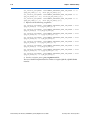
ctl_mem_cs_n_h
■
ctl_mem_ras_n_h
■
ctl_mem_we_n_h
■
ctl_mem_odt_h
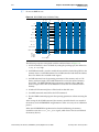
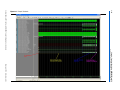
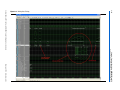
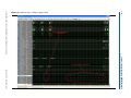
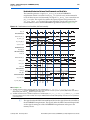
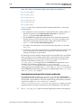
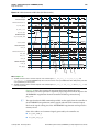
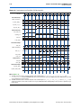
As can be seen in the waveform (Figure 3–13), the sequence of commands are
PreCharge (PCH), ACT, and NOP, followed by a series of write commands.
1. The controller puts the five consecutive write commands with a starting address of
0 × with increments of four (0000, 0004, 0008, 000c, 0010), see the top of Figure 3–13
under the PHY Command Input label.
2. The controller generates the following signals two clock cycles after
ctl_mem_wdata_valid and must supply the data ctl_mem_wdata along with
these two clock cycles. Refer to Figure 3–13 under the PHY Write Data Input label.
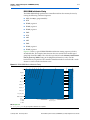
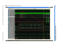
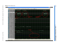
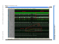
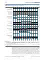
3. The ALTMEMPHY megafunction generates the write command at the memory
interface after five-to-seven memory clock (mem_clk) cycles (to accommodate the
write delay). In this example, the address and commands are generated using the
negative edge of the memory clock, see Figure 3–14 under the PHY Command
Output label.
4. The address and commands are of 2T period and the chip select is of 1T period.
5. The data (mem_dq) at the memory interface is presented after two memory clock
cycles of write latency. The write latency is equal to the CAS latency -1 for DDR2
SDRAM only (for DDR SDRAM it is always 1). For this example, CAS latency is
equal to three.
6. The generation of DQS signals is controlled using the
control_mem_wdata_valid signal, which is very important as the generation
of the DQS signal is also dependent on the CAS latency parameter.
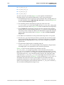
Figure 3–13 shows that the controller state machine asserts the
ctl_mem_wdata_valid signal to perform a write transaction. The write data
(ctl_mem_wdata) should be available at the same time when the signal is asserted
high. The ctl_mem_wdata_valid signal is asserted for five clock cycles (phy_clk)
or ten clock cycles (mem_clk) to transfer five data transfers. The write data is only
valid when the ctl_mem_wdata_valid is asserted high and is held in the wdata
registers until the write occurs. In Figure 3–13, the write data bus ctl_mem_wdata is
of width 64 and each burst transfer is of the length four. The 64-bit wide data is
transferred to the memory as four 16-bit wide data, as shown by mem_dq. The DQS
clock is twice the frequency of the clock that clocks the ctl_mem_wdata and the DQ
data is transferred during both the edges of DQS.
External Memory PHY Interface (ALTMEMPHY) (nonAFI) Megafunction User Guide
© January 2010 Altera Corporation