1
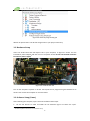
EPEE User Guide
Jian Gong ([email protected])
1. Hardware Interface
The hardware interface consists of UCR (user controllable register), DMA (direct memory access)
and UDI (user defined interrupt) interfaces, as figure 1.1 shows. The DMA interface can be used
for transferring large amount of data. The UCR and UDI interface can be used to control the
hardware.
Hardware (FPGA) Application
UCR
DMA
UDI
Software Application
UCR
DMA
Zero-Copy
UDI
Figure 1.1 EPEE user interface
1.1. DMA Interface
DMA interface can be divided into host to board (DMA read) part and board to host (DMA write)
part. FIFO1 is used as the interface. Table 1.1 illustrates the DMA interface.
Table 1.1 DMA Interface
Name
I/O
Description
64 bit interface:
FIFO_host2board_dout[71:0]
128 bit interface2
FIFO_host2board_dout[129:0]
output
DMA host to board (DMA read) data output.
64 bit interface
Data will be transferred in bits 63~0. Bit 65 indicates
dout[63:23] contains valid data; bit 64 indicates
dout[31:0] contains valid data.
128 bit interface
Data will be transferred in bits 127~0. Bit 129~128
indicates whether the QWs (8 Byte) in 127~64 and
63~0 contains valid data.
FIFO_host2board_empty
output
Empty signal of Xilinx FIFO. (The FIFO is a First-Word
Fall-Through FIFO)
FIFO_host2board_rd_en
input
Read enable signal of Xilinx FIFO.
1
For more information of Xilinx FIFO, please see Xilinx PG057,” LogiCORE IP FIFO Generator”. The FIFO we use is
native interface FIFO with First-Word Fall-Through.
2
The PCIe Gen2 X8 mode uses the 128 bit interface.
1
64 bit interface:
FIFO_board2host_din[71:0]
128 bit interface:
FIFO_host2board_din[129:0]
input
DMA board to host (DMA write) data input.
64 bit interface
Data should be transferred in bits 63~0. Bit 65~64
indicates whether the DWs (4 bytes) in 63~32 and
31~0 are valid.
128 bit interface
Data should be transferred in bit 127~0. Bit 129~128
indicates whether the QWs (8 Byte) in 127~64 and
63~0 are valid.
FIFO_board2host_prog_full
output
FIFO’s program full signal. This FIFO’s depth is 512. It is
configured to assert program full if it contains more
than 500 items.
FIFO_board2host_wr_en
output
Write enable signal of Xilinx FIFO.
For host to board side interface (take 64 bit interface as an example),
FIFO_host2board_dout[65:64] = 2’b00 will never occur. Data within one DMA transaction will be
continuous, that is, FIFO_host2board_dout[65:64] can be 2’b10 only in the last DW of a DMA
transaction.
For example, when software wants to DMA 2N (N = 1, 2, 3…) DWs (1 DW = 4 Byte) to board,
FIFO_host2board_dout[65:64] will always be 2’b11, as figure 1.2 shows. If DMA 2N-1 DWs to
board, the last data in FIFO_host2board will let FIFO_host2board_dout[65:64] be 2’b10,
indicating FIFO_host2board_dout[31:0] is invalid this cycle.
1
2
3
4
5
6
7
8
9
10
clk
FIFO_host2board_rd_en
FIFO_host2board_empty
FIFO_host2board_dout[65:64]
2'b11
2'b11
2'b10
FIFO_host2board_dout[63:32]
DW0
DW2
DW 2N-1
FIFO_host2board_dout[31:0]
DW1
DW3
DW 2N
TimeGen
Figure 1.2 Timing of host2board FIFO (2N data)
1
2
3
4
5
6
7
8
9
10
clk
FIFO_host2board_rd_en
FIFO_host2board_empty
FIFO_host2board_dout[65:64]
2'b11
2'b11
2'b10
FIFO_host2board_dout[63:32]
DW0
DW2
DW 2N-1
FIFO_host2board_dout[31:0]
DW1
DW3
TimeGen
Figure 1.3 Timing of host2board FIFO (2N-1 data)
2
Timing for 128 bit interface is like that of the 64 bit interface. Data within one DMA transaction
from host to board will be continuous. Only in the last cycle, the FIFO_host2board_dout[129:128]
can be 2’b10.
For board to host side interface (take 64 bit interface as an example), user can assert and
deassert FIFO_board2host_din[65:64] at any time. EPEE will pack data for user and software will
see continuous data. As figure 1.4 and 1.5 shows, in software side, continuous data DW0, DW1,
DW2, DW3, DW4 will be seen.
1
2
3
4
5
6
7
8
9
10
clk
FIFO_board2host_wr_en
FIFO_board2host_prog_full
FIFO_board2host_din[65:64]
2'b11
2'b11
2'b10
FIFO_board2host_din[63:32]
DW0
DW2
DW4
FIFO_board2host_din[31:0]
DW1
DW3
TimeGen
Figure 1.4 Timing of board2host FIFO
1
2
3
4
5
6
7
8
9
10
clk
FIFO_board2host_wr_en
FIFO_board2host_prog_full
FIFO_board2host_din[65:64]
2'b11
2'b10
FIFO_board2host_din[63:32]
DW0
DW2
FIFO_board2host_din[31:0]
DW1
2'b01
2'b10
DW4
DW3
TimeGen
Figure 1.5 Timing of board2host FIFO 2
1.2. UCR Interface
PIO read and PIO write bus make the UCR interface. User can define controllable register with
these bus signals. The PIO bus signals are listed in table 1.2.
Table 1.2 UCR interface signals
Name
I/O
Description
usr_pio_rd_req
Output
Read request in PIO bus.
usr_pio_rd_ack
Input
Read acknowledge in PIO bus. It should be asserted for one
cycle after usr_pio_rd_req asserted and data prepared in
usr_pio_rd_data.
3
usr_pio_rd_addr[16:0]
Output
Read address. It is only valid when usr_pio_rd_req asserted.
usr_pio_rd_data[31:0]
Input
The read data. It should be prepared when usr_pio_rd_ack
asserted.
usr_pio_wr_req
Output
Write request in PIO bus.
usr_pio_wr_ack
Input
Write acknowledge in PIO bus. Assert it for one cycle when
data is written into register.
usr_pio_wr_addr[16:0]
Output
Write address, it is valid when usr_pio_wr_req asserted
usr_pio_wr_data[31:0]
Output
Write data, it is valid when usr_pio_wr_req asserted
1
2
3
4
5
6
7
8
9
10
clk
usr_pio_rd_req
usr_pio_rd_ack
usr_pio_rd_addr
Addr
usr_pio_rd_data
Data
TimeGen
Figure 1.6 UCR read timing
1
2
3
4
5
6
7
8
9
10
clk
usr_pio_wr_req
usr_pio_wr_ack
usr_pio_wr_addr
Addr
usr_pio_wr_data
Data
TimeGen
Figure 1.7 UCR write timing
1.3. UDI Interface
The UDI interface supports up to 8 interrupts. The signals are listed in table 1.3
Table 1.3 UDI interface signals
Name
I/O
Description
usr_int_req
Input
User interrupt request. Assert to send an interrupt. The
usr_int_req signal should be asserted until usr_int_clr is
asserted.
usr_int_vector[2:0]
Input
Interrupt vector, indicating which interrupt will be sent. EPEE
4
support 8 interrupts currently.
usr_int_sw_waiting[7:0]
Output
Indicates whether software is waiting for the interrupt occur.
Software calling function “block_until_interrupt” will cause
corresponding bit to be asserted.
usr_int_clr
Output
Clear the interrupt.
usr_int_enable
Output
User interrupt enable signal.
After user software call function “block_until_interrupt(vector_num)”, it will be blocked and
usr_int_sw_waiting [vector_num] (in hardware side) will be asserted. If hardware send an
interrupt with usr_int_vector[2:0] = usr_int_sw_waiting, that software will be waked up and
usr_int_sw_waiting [vector_num] will deassert.
Figure 1.8 shows how interrupt with “vector = 1” works. A software process called
block_until_interrupt(1) function before clock edge “2”, so the usr_int_sw_waiting’s bit 1 is
asserted. After the interrupt finished and that process has been waked up, that bit is deasserted.
1
2
3
4
5
6
7
8
9
10
clk
usr_int_enable
usr_int_req
usr_int_clr
usr_int_vector
usr_int_sw_waiting
3'd1
8'b00000000
8'b00000010
8'b00000000
TimeGen
Figure 1.8 User defined interrupt interface timing
2. Software API Definition
The software APIs are in sPcie.h and sPcieZerocopy.h. The APIs can be divided into DMA (direct
memory access), UCR (user controllable register), UDI (user defined interrupt) and Zero-Copy
DMA parts. Besides these APIs, we also provide some other APIs such as the reset API. These APIs
are listed in table 2.1~2.5.
Note: For 64 bit interface, DMA data should be an integral multiple of DW (4Byte); for 128 bit
interface hardware, DMA data should be an integral multiple of QW (8Byte).
Table 2.1 DMA APIs
API Name
Function
dma_host2board
DMA data from host to board. It will block until DMA is done.
dma_host2board_unblocking
DMA data from host to board. Return immediately after the DMA
is started. If hardware is currently busy, it will return -1.
dma_board2host
DMA data from board to host. It will block until DMA is done.
5
get_host2board_count
Return the number of DWs that has been DMA from host to
board. It can be used for debugging.
get_board2host_count
Return the number of DWs that has gone through FIFO
board2host. It can be used for debugging.
Table 2.2 UCR APIs
API Name
Function
read_usr_reg
Read a user controllable register
write_usr_reg
Write a user controllable register
Table 2.3 UDI APIs
API Name
Function
block_until_interrupt
Block until the corresponding interrupt occur.
Table 2.4 Zero-Copy APIs
API Name
Function
get_zerocopy_buffer
Get zerocopy buffer. The buffer size is defined by macro BUF_SIZE
release_zerocopy_buffer
Release the zerocopy buffer.
zerocopy_host2board
DMA data from host to board
zerocopy_board2host
DMA data from board to host
get_host2board_status
Get host to board status
get_board2host_status
Get board to host status
Table 2.5 Other APIs
API Name
Function
get_pcie_cfg_mode
Return the configured PCIe mode. E.g. Gen2 X4
get_pcie_cur_mode
Return the currently used PCIe mode.
sys_reset
Reset the whole system
usr_reset
Reset the user hardware
host2board_reset
Reset host to board side DMA data transfer, including the FIFO
host2board
board2host_reset
Reset board to host side DMA data transfer, including the FIFO
board2host
3. Example Design
3.1. Generate the Example Design
Take the VC707 for example. Extract the source code to V7_485T_X4Gen2 (as figure 3.1 shows).
6
Figure 3.1 Extracted source files (in folder V7_485T_X4Gen2)
Open an ISE project navigator, use file->new project to make a new project. Then choose the
“Virtex-7 VC707 Evaluation Platform” in “Evaluation Development Board” option to specify to the
VC707 board. As figure 3.2 shows.
Figure 3.2 Project settings
Add all the source files in V7_485T_X4Gen2 folder into the ISE project. Then we can see the
hierarchy of the source code, which is as figure 3.3 shows.
Figure 3.3 Project hierarchy
Select the top level “demo_top_x4gen2” then double click the “Generate Programming File” in
Process window (Figure 3.4).
7
Figure 3.4 Generate programming file
Wait for all process done. The bit file will generate in your project’s directory.
3.2. Hardware Setup
Insert the VC707 board into PCI Express slot in your computer, as figure 3.5 shows. Use the
included PC power adaptor and then turn on the power switch. Do not use the PCIe connector
from the PC power supply!3
Figure 3.5 VC707 in PCIe slot
Turn on the computer to power on VC707. Use Impact tool to program the generated bit file to
VC707. Then restart the computer to reset the board.
3.3. Software Setup (Linux)
After rebooting the computer, open a terminal and follow these steps.
1. List the PCI devices to make sure EPEE can be detected. Figure 3.6 shows the “lspci”
3
See Xilinx xtp144 for details on the hardware setup.
8
command lists all the PCI devices (including PCIe devices) and Xilinx board VC707 with EPEE
can be detected (the Xilinx Corporation Device 7024).
Figure 3.6 List PCI devices
2. Make the driver module. The following commands require sudo privilege, so we use “sudo su”
to change to root user.
Figure 3.7 Make the driver module
3. Insert the driver module with make_device script
Figure 3.8 insert driver module into Linux kernel
4. Go to directory “app”
$ cd ../app
5. Make test applications with the make.sh script
Figure 3.9 Compile test applications
6. DMA test: The DMA length is from 8 to 4096 bytes, increasing 8 byte each time. For each
9
DMA, the DMA_test program firstly DMA data from host to board, then DMA data from
board to host. The user hardware (see USER_HW/usr_dma.v) bit wises the data from host.
The DMA_test program will check whether the data from board are bitwise from the original
data. If no error occurred as figure 3.10 shows, the test passed.
Figure 3.10 Run DMA test
7. PIO test
Figure 3.11 PIO test
In this test, the PIO_test program firstly writes 1 to reg0, and then writes 2 to reg1. Then it
read reg2 and reg3. The reg2 and reg3 are read only by software side. User hardware in this
demo calculates reg2 and reg3 this way (see USER_HW/usr_pio.v):
reg_2 <= reg_0 - reg_1;
reg_3 <= reg_0 + reg_1;
8. UDI test
10
Figure 3.12 UDI test
3.4. About the Example Design
The structure of the example design is illustrated in figure 3.13. There are three main parts of the
example design. The PCIE_TOP module is the main part of EPEE library (hardware side). Xilinx
PCIe IP core is in CORE_WRAPPER module of PCIE_TOP. The EXTEN_LIB part consists of four clock
switch module and a RESET_GEN module. These five modules do clock domain switch between
EPEE library and user hardware. The USER_HW contains three small demos for UCR (PIO), DMA
and UDI interfaces.
The usr_pio module has four registers in it. Reg 0 and reg 1 can be read and written by software
while reg 2 and reg 3 are read only. The value of reg 2 and reg 3 follows these equations.
Reg2 = reg 0 + reg1
Reg3 = reg0 – reg1
PCIE_TOP
EXTEN_LIB
USER_HW
RESET_GEN
PIO_CLK_ SWITCH
usr_pio
BUS_MASTER
CORE_WRAPPER
Xilinx PCIe IP Core
PCIe Bus
DMA_HOST2BOARD
_CLK_SWITCH
usr_dma
DMA_BOARD2HOST
_CLK_SWITCH
USR_INT_
MANAGER
Figure 3.13 Example design structure
11
usr_int
Module usr_dma loop each data from host2board fifo back to board2host fifo. It also does
bitwise operation to each data.
Module usr_int generates two kinds of user defined interrupts (vector 0 and vector 1). When
software is waiting for interrupt, the counter inside this module will count. Interrupt will be
generate when the counter reach a certain number (10 for vector 0 and 1000 for vector 1).
3.5. About Xilinx PCIe Core
The Xilinx PCIe core is in CORE_WRAPPER/*_1Mbar directory. User can also generate the IP core.
If one wants to generate the IP core, he (she) can follow these steps.
The component name of the core should be assigned to “PCIE_CORE_1MBar”, as the figure 3.14
shows.
Figure 3.14 Modify the name of component
The base address register is 1MB with 64 bit enabled, and only Bar0 is used in EPEE, which is
shown in figure 3.15.
Figure 3.15 Base address registers option
12
For the other options, the default option can be used.
Note: For 7 series integrated block for PCI Express, there is some problem that the Intel Z77
chipset can’t detect the board. It is a known issue which is recorded by Xilinx AR# 51135. See
http://www.xilinx.com/support/answers/51135.html for details.
Note: For KC705 evaluation board, the UCF differs between different revisions of board. The
following line should be changed (in UCF):
INST "PCIE_TOP/CORE_WRAPPER/refclk_ibuf" LOC = IBUFDS_GTE2_X0Y1;
Revision of KC705
Location constrain (LOC)
Rev. A
IBUFDS_GTE2_X0Y3
Rev. B / Rev. C
IBUFDS_GTE2_X0Y1
13