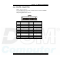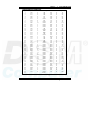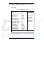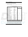
1
USER’S
MANUAL
96D2641
VIA EDEN Half-size
Embedded Card
With VGA/LAN/SOUND
Copyright Notice
Half-size CPU Board
With VGA / Sound / LAN
OPERATION MANUAL
COPYRIGHT NOTICE
This operation manual is meant to assist both Embedded Computer
manufacturers and end-users in installing and setting up the system. The
information contained in this document is subject to change without any
prior notice.
This manual is copyrighted March 21, 2003. You may not reproduce or
transmit in any form or by any means, electronic, or mechanical, including
photocopying and recording.
ACKNOWLEDGEMENTS
All trademarks and registered trademarks mentioned herein are the property
of their respective owners.
Contents
TABLE OF CONTENTS
CHAPTER
1-1
1-2
1-3
1
INTRODUCTION
About This Manual .......................................................
System Specifications ...................................................
Safety Precautions .........................................................
CHAPTER
2
1-2
1-3
1-6
HARDWARE CONFIGURATION
2-1
Jumper & Connector Quick Reference Table ...............
2-2
Component Locations ...................................................
2-3
How to Set the Jumpers ................................................
2-4
COM Port Connector ....................................................
2-5
RS232/422/485 (COM2) Selection ...............................
2-6
Keyboard/Mouse Connector ……………….................
2-7
Keyboard/Mouse Selection ..........................…………
2-8 External Speaker Connector ..........................................
2-9 Inverter Connector …………………………………….
2-10 Power LED Connector ..........................………………
2-11 Reset Connector ............................................................
2-12 Hard Disk Drive LED Connector ..................................
2-13 Power Button ………………………………………….
2-14 External Buzzer Connector …………………………
2-15 SLPBTN Connector .............….............………………
2-16 Fan Connector ………………………………………
2-17 IrDA Connector ……………………………………….
2-18 VGA Connector ………................................................
2-19 LCD Connector …………………………………….…
2-20 Universal Serial Bus Connector ………………………
2-21 Clear CMOS Selection ………………………………..
2-22 Floppy Disk Drive Connector .......................................
2-23 Hard Disk Drive Connector ..........................................
2-24 Printer Connector ..........................................................
2-25 Reset/NMI/Clear Watchdog Selection ………………..
2-26 LAN Connector ............................................................
2-27 ATX Power Connector ………………………………..
2-28 ATX Backplane Connector …………………………
2-29 AT/ATX Power Selection .............................................
2-30 Sound Connector ……………………………………...
2-31 CD Audio-In Connector ………………………………
2-32 Solid-State Disk Socket ................................................
2-2
2-3
2-4
2-6
2-7
2-7
2-8
2-8
2-9
2-9
2-9
2-10
2-10
2-10
2-11
2-11
2-11
2-12
2-13
2-14
2-14
2-15
2-16
2-17
2-18
2-19
2-19
2-20
2-20
2-21
2-21
2-22
Contents
2-33
2-34
2-35
2-36
SSD Memory Mapping Selection …………………….
IRQ12 Release Selection ……………………………...
LVDS LCD Connector ………………………………..
LVDS Panel Power Selection ………………………...
CHAPTER
3-1
3-2
3-3
3-4
3-5
3-6
SOFTWARE UTILITIES
Introduction ...................................................................
VGA Driver Utility .......................................................
Flash BIOS Update .......................................................
LAN Driver Utility …...................................................
Sound Driver Utility …………………………………..
Watchdog Timer Configuration ....................................
CHAPTER
4-1
4-2
4-3
4-4
4-5
4-6
4-7
4-8
4-9
4-10
4-11
4-12
4-13
4-14
4-15
3
4
A
B
4-2
4-3
4-4
4-8
4-12
4-16
4-19
4-22
4-24
4-25
4-26
4-26
4-27
4-28
4-29
EXPANSION BUS
PC/104 Plus Bus Connector Pin Assignment ...........................
Compact Flash Card Connector Pin Assignment .....................
APPENDIX
3-2
3-2
3-3
3-5
3-7
3-8
AWARD BIOS SETUP
Introduction ...................................................................
Entering Setup ...............................................................
The Standard CMOS Features ……..............................
The Advanced BIOS Features …...................................
Advanced Chipset Features ...........................................
Integrated Peripherals ……...........................................
Power Management Setup ............................................
PNP/PCI Configuration ………………………………
PC Health Status ………………………………………
Frequency/Voltage Control …………………………
Load Fail-Safe Defaults ................................................
Load Optimized Defaults ..............................................
Password Setting ...........................................................
Save & Exit Setup .........................................................
Exit Without Saving ......................................................
APPENDIX
2-23
2-23
2-24
2-24
A-2
A-3
TECHNICAL SUMMARY
Block Diagram .........................................................................
Interrupt Map ............................................................................
RTC & CMOS RAM Map .......................................................
Timer & DMA Channels Map ..................................................
I/O & Memory Map .................................................................
B-2
B-3
B-4
B-5
B-6
Contents
APPENDIX
C
TROUBLESHOOTING
Troubleshooting for Error Messages ......................................
Troubleshooting for POST Code ............................................
C-2
C-5
CHAPTER
INTRODUCTION
1
This chapter gives you the information . It also
outlines the System specifications.
Section includes:
z About This Manual
z System Specifications
z Safety precautions
Experienced users can skip to chapter 2 on page 2-1
for a Quick Start.
Page:1-1
Chapter
1
Introduction
1-1. ABOUT THIS MANUAL
Thank you for purchasing , Half Size CPU Board enhanced
with VGA/Sound/LAN, is fully PC / AT compatible. The
provides faster processing speed, greater expandability and can handle
more tasks than before. This manual is designed to assist you how to install
and set up the system. It contains four chapters. The user can apply this
manual for configuration according to the following chapters :
Chapter 1 Introduction
This chapter introduces you to the background of this manual, and the
specifications for this system. The final page of this chapter will indicate
how to avoid damaging this Embedded Board.
Chapter 2 Hardware Configuration
This chapter outlines the component locations and their functions. In the
end of this chapter, you will learn how to set jumper and how to configure
this card to meet your own needs.
Chapter 3 Software Utilities
This chapter contains helpful information for proper installations of the
VGA Utility, LAN Utility, Sound Utility, and Flash BIOS Update. It also
describes the Watchdog-timer configuration.
Chapter 4 Award BIOS Setup
This chapter indicates you how to set up the BIOS configurations.
Appendix A Expansion Bus
This Appendix introduces you the expansion bus for PC/104.
Appendix B Technical Summary
This section gives you the information about the Technical maps.
Appendix C Trouble Shooting
This section outlines the error messages and offers you the methods to
solve the problems.
Page: 1-2
USER′S MANUAL
Chapter
1
Introduction
1-2. SYSTEM SPECIFICATIONS
z CPU :
VIA Eden 400/667 MHz processors
Auto detect voltage regulator.
z SYSTEM CHIPSET :
VIA VT8606, VT82C686B
z MEMORY :
Up to 512MB SDRAM
One 144-pin SO-DIMM socket on board.
z CACHE :
Built-in CPU.
z REAL-TIME CLOCK / CALENDAR :
CMOS data back up from BIOS set or BIOS default.
Built-in VIA VT82C686B.
External 5.0V Real Time Clock (Optional).
z BIOS :
PhoenixAward PnP BIOS Memory size 2 Mbytes, with VGA BIOS.
Easy update 256KB flash EEPROM.
Supports Green Function.
Supports S/IO Setup.
z KEYBOARD CONNECTOR :
PS/2 keyboard with mini DIN connector or one external 5-pin boxheader
connector with mini DIN cable
Supports Y-Cable.
z MOUSE CONNECTOR :
PS/2 mouse connector with min DIN cable
Selectable with keyboard DIN connector
z BUS SUPPORT :
PC/104 Bus
ISA Bus
USER′S MANUAL
Page: 1-3
Chapter
1
Introduction
z DISPLAY :
Built-in VIA VT8606, supports CRT, TTL & LVDS.
Integrated S3®’s Savage4™ 2D/3D/Video Accelerator.
Optimized Shared Memory Architecture (SMA).
2~32 MB Frame Buffer using system memory.
Supports simultaneous display of CRT & LCD.
Interface:
One 15-pin connector supports for CRT Monitor.
One 41-pin connector support 18 bit or 24 bit panel for TTL.
One 30-pin connector support 2x18 bit LVDS panel.
z WATCHDOG :
I / O port 0443H to Enable watchdog.
I / O port 0441H to Disable watchdog.
Selectable for Reset / NMI Watchdog function.
Time-out timing select 0 / 8 / 16 / 24 / 32 / 40 / 48 / 56 / 64 / 72 / 80 / 88 /
96 / 104 / 112 / 120 sec +/- 25%.
z IDE INTERFACE :
One EIDE port supports Ultra DMA-100/66/33.
One channel supports up to two devices.
z FLOPPY DISK DRIVER INTERFACE :
Supports up to two Floppy Disk Drives, 3.5" and 5.25" (1.44M / 2.88M).
z USB CONNECTOR :
Universal Serial Bus Connector, supports up to two USB1.1 ports.
z LAN ADAPTER :
Realtek 8100BL PCI Fast Ethernet
10/100 Base-TX PCI-BUS
z SERIAL PORT :
Two high speed 16550 Compatible UARTs with Send / Receive 16 Byte
FIFOs; COM1 for RS-232; COM2 for RS-232/422/485
COM1 with two 5-pin boxheader connector on board
COM2 with 9-pin D-SUB connector on board
Infrared Communications port option on the COM2.
Page: 1-4
USER′S MANUAL
Chapter
1
Introduction
z PARALLEL PORT :
Supports SPP, ECP, EPP Function mode.
Bi-directional parallel port.
z SOUND FUNCTION :
Integrated Sound Blaster / DirectSound AC97 audio.
Dual Full duplex direct sound channels bet. system memory & AC97 link.
32 byte FIFO of each Direct Sound Channel.
Realtek ALC201, AC97 SoundMAX® Codec
Interface: MIC, line-out, and speaker.
z GREEN FUNCTION :
Software supported by BIOS setup.
Hardware supported by switch control.
z Solid-State Disk Socket :
Memory System DiskOnChip SSD Module support up to 288MB.
z HARDWARE MONITORING FUNCTION :
Monitor CPU Voltage, CPU temperature, and Cooling Fan.
z LED INDICATOR :
HDD LED: one 2-pin headpin on board
power LED: one 2-pin headpin on board
z DMA CONTROLLER :
82C37 x 2
z DMA CHANNELS :
7
z INTERRUPT CONTROLLERS :
82C59 x 2
USER′S MANUAL
Page: 1-5
Chapter
1
Introduction
z INTERRUPT LEVELS :
15
z OPERATING TEMPERATURE :
0 to 60°C (32°F to 140°F)
z SYSTEM POWER REQUIREMENT :
DC Voltage: +5V Standby, minimum +4.75V, maximum +5.25V.
DC Ampere: 0.04A. (ATX Support)
DC Voltage: +5V, minimum +4.75V, maximum +5.25V.
DC Ampere: 2.4A.
DC Voltage: +12V, minimum +11.4V, maximum +12.6V.
DC Ampere: 0.2A.
z BOARD DIMENSION :
185mm x 122mm (7.28” x 4.8”)
z BOARD NET WEIGHT :
280g (0.616 lb)
1-3. SAFETY PRECAUTIONS
Follow the messages below to avoid your systems from damage:
1. Keep your system away from static electricity on all occasions.
2. Prevent electric shock. Don‘t touch any components of this card when
the card is power-on. Always disconnect power when the system is not
in use.
3. Disconnect power when you change any hardware devices. For instance,
when you connect a jumper or install any cards, a surge of power may
damage the electronic components or the whole system.
Page: 1-6
USER′S MANUAL
HARDWARE
CONFIGURATION
CHAPTER
2
** QUICK START **
Helpful information describes the jumper & connector settings, and
component locations.
This section includes:
z Jumper & Connector Quick Reference Table
z Component Locations
z Configuration and Jumper settings
z Connector‘s Pin Assignments
Page 2-1
Chapter
2
Hardware Configuration
2-1. JUMPER & CONNECTOR QUICK REFERENCE TABLE
COM Connector .................................................……….
RS232/422/485 (COM2) Selection ......................……...
Keyboard/Mouse Connector ………..……....….............
Keyboard/Mouse Selection …………………………….
External Speaker Connector ................................………
Inverter Connector ……………………………………...
Power LED Connector …………………………………
Reset Connector ...................................................……..
Hard Disk Drive LED Connector ........................………
Power Button …………………………………………...
External Buzzer Connector …………………………….
SLPBTN Connector ……………………………….…...
Fan Connector ………………………………………….
IrDA Connector ………………………………………...
VGA Connector ……….......................................……...
LCD Connector ……………………………………….
Universal Serial Bus Connector ...........................……...
Clear CMOS Selection ………………………….……...
Floppy Disk Drive Connector ..............................……...
Hard Disk Drive Connector .................................……...
Printer Connector .................................................……..
NMI/Reset/Clear Watchdog …………………..………..
LAN Connector ...................................................………
ATX Power Connector ..………………………………..
ATX Backplane Connector …………………………….
AT/ATX Power Selection ..………………………….
Sound Connector …….………………………….……...
CD Audio-in Connector ………………………………..
Solid-State Disk Socket ………………………………..
SSD Memory Mapping Selection ………………………
IRQ12 Release Selection ……………………………….
LVDS LCD Connector …………………………………
LVDS Panel Power Selection ………………………….
Page: 2-2
COM1, COM2
JP2
KB1
JP10
EXKB1
INV1
JP4 (1-3)
JP4 (9-10)
JP4 (2-4)
JP4 (5-6)
JP4 (7-8)
JP4 (13-14)
FAN1
IR1
VGA1
LCD1
CN2
JP7
FDD1
IDE1
LPT1
JP8
UTP1
PW1
JP9
J2, J3
CN1
CD_IN1
SSD
JP1
J1
LVDS1
JP3
USER′S MANUAL
Chapter
2
Hardware Configuration
2-2. COMPONENT LOCATIONS
IDE1
30
29
JP3
JP2
JP4
EXKB1
2
LVDS1
VT8606
Battery
JP7
JP8
2 1 1
RTC
VIA
EDEN
FAN1
2 1
1
1
JP9
CN2
5
6
1
2
JP10
10 5
Connector, Jumper and Component locations
USER′S MANUAL
Page: 2-3
Chapter
2
Hardware Configuration
2-3. HOW TO SET THE JUMPERS
You can configure your board by setting the jumpers. Jumper is consists of
two or three metal pins with a plastic base mounted on the card, and by using
a small plastic "cap", Also known as the jumper cap (with a metal contact
inside), you are able to connect the pins. So you can set-up your hardware
configuration by "opening" or "closing" pins.
The jumper can be combined into sets that called jumper blocks. When the
jumpers are all in the block, you have to put them together to set up the
hardware configuration. The figure below shows how this looks like.
JUMPERS AND CAPS
If a jumper has three pins (for example, labelled PIN1, PIN2, and PIN3), You
can connect PIN1 & PIN2 to create one setting and shorting. You can either
connect PIN2 & PIN3 to create another setting. The same jumper diagrams are
applied all through this manual. The figure below shows what the manual
diagram looks like and what they represent.
Page: 2-4
USER′S MANUAL
Chapter
2
Hardware Configuration
JUMPER DIAGRAMS
JUMPER SETTINGS
USER′S MANUAL
Page: 2-5
Chapter
2
Hardware Configuration
2-4. COM PORT CONNECTOR
There are two COM ports enhanced in this board namely: COM1 and
COM2. COM1 is fixed for RS-232, while COM2 is selectable for RS232/422/485.
COM1 : COM1 Connector
The COM1 Connector assignments are as follows :
PIN
1
2
3
4
5
6
7
8
9
10
ASSIGNMENT
DCD
RX
TX
DTR
GND
DSR
RTS
CTS
RI / +5V / +12V selectable
NC
5
1
9
6
COM1
COM2 : COM2 Connector
The COM2 Connector assignments are as follows :
PIN
1
2
3
4
5
6
7
8
9
10
Page: 2-6
ASSIGNMENT
RS-422
RS-485
TXTXTX+
TX+
RX+
RX+
RXRXGND
GND
RTSNC
RTS+
NC
CTS+
NC
RI/+5V/+12
CTSNC
NC
NC
NC
RS-232
DCD
RX
TX
DTR
GND
DSR
RTS
CTS
5
1
10
6
COM 2
USER′S MANUAL
Chapter
2
Hardware Configuration
2-5. RS232/422/485 (COM2) SELECTION
JP2 : RS-232/422/485 Selection
COM2 is selectable for RS-232, 422, 485 function.
The jumper settings are as follows :
COM 2
FUNCTION
JUMPER SETTING
(pin closed)
RS-232
Open
RS-422
1-2, 5-6, 7-8, 9-10
11-12, 13-14, 15-16
17-18, 19-20
RS-485
1-3, 4-6, 7-8, 9-10
11-12, 13-14, 15-16
17-18, 19-20
JUMPER
ILLUSTRATION
*** Manufactory default --- RS-232.
2-6. KEYBOARD/MOUSE CONNECTOR
USER′S MANUAL
2 1
3
6
ASSIGNMENT
KBDATA
MSDATA
GND
KBVCC
KBCLK
MSCLK
4
PIN
1
2
3
4
5
6
5
KB1 : Keyboard/Mouse Connector
The jumper settings are as follows:
KB1
Page: 2-7
Chapter
2
Hardware Configuration
2-7. KEYBOARD/MOUSE SELECTION
JP10 : Keyboard or Mouse Selection.
If User select to use Y-Cable, please set the jumper same as AT Keyboard.
The selections are as follows :
DEVICE
TYPE
JUMPER SETTING
KEYBOARD/Y-Cable
3-5
4-6
5
6
1-3
2-4
5
6
PS/2 MOUSE
(pin closed)
JUMPER
ILLUSTRATION
JP10
JP10
1
2
1
2
*** Manufactory default -- AT Keyboard
2-8. EXTERNAL KEYBOARD CONNECTOR
EXKB1 : External Keyboard Connector.
The pin assignments are as follows:
PIN
1
2
3
4
5
Page: 2-8
ASSIGNMENT
KBCLK
KBDATA
NC
GND
VCC
USER′S MANUAL
Chapter
2
Hardware Configuration
2-9. INVERTER CONNECTOR
INV1 : Inverter Connector
The pin assignment is as follows:
PIN
1
2
3
4
5
6
ASSIGNMENT
+12V
+12V
GND
VCC
GND
ENABKL (Inverter backlight
ON/OFF control signal)
1
2-10. POWER LED CONNECTOR
JP4 (1-3) : Power LED Connector
The pin assignment is as follows:
PW_LED
PIN
1
3
ASSIGNMENT
PW_LED
GND
JP4
2-11. RESET CONNECTOR
JP4 (9-10) : Reset Connector.
The pin assignments are as follows :
RST
PIN
9
10
ASSIGNMENT
GROUND
RESET
USER′S MANUAL
JP4
Page: 2-9
Chapter
2
Hardware Configuration
2-12. HARD DISK DRIVE LED CONNECTOR
JP4 (2-4) : Hard Disk Drive LED Connector
The pin assignments are as follows :
HDD _LED
PIN
2
4
ASSIGNMENT
VCC
HDD Active Signal
JP4
2-13. POWER BUTTON
JP4 (5-6) : Power Button for ATX power.
The pin assignments are as follows:
PIN
5
6
PW_BN
ASSIGNMENT
GROUND
PW_BN
JP4
2-14. EXTERNAL BUZZER CONNECTOR
JP4 (7-8) : External Buzzer Connector
The pin assignments are as follows:
EXT_BUZ
PIN
7
8
Page: 2-10
ASSIGNMENT
E_BUZ
VCC
JP4
USER′S MANUAL
Chapter
2
Hardware Configuration
2-15. SLPBTN CONNECTOR
JP4 (13-14) : SLPBTN Connector
The pin assignments are as follows:
SLPBTN
PIN
13
14
ASSIGNMENT
GND
SLPBTN
JP4
2-16. FAN CONNECTOR
FAN1 : FAN Connector
The pin assignments are as follows:
PIN
1
2
3
ASSIGNMENT
GND
+12V
FAN speed monitor
FAN1
1
2-17. IRDA CONNECTOR
IR1 : IrDA (SIR) Connector
The pin assignments are as follows:
PIN
1
2
3
4
5
ASSIGNMENT
VCC
NC
IRRX
GND
IRTX
USER′S MANUAL
Page: 2-11
Chapter
2
Hardware Configuration
2-18. VGA CONNECTOR
VGA1 : VGA Connector
The pin assignments are as follows:
PIN
1
2
3
4
5
6
7
8
9
10
11
12
13
14
15
Page: 2-12
ASSIGNMENT
RED
GREEN
BLUE
NC
GND
GND
GND
GND
NC
GND
NC
I2CCK
HSYNC
VSYNC
I2CDA
6
11
1
5
10
15
VGA
USER′S MANUAL
Chapter
2
Hardware Configuration
2-19. LCD CONNECTOR
LCD1 : LCD Connector
The pin assignments are as follows :
PIN
1
3
5
7
9
11
13
15
17
19
21
23
25
27
29
31
33
35
37
39
41
ASSIGNMEN
T
P20
P16
P21
P17
P22
P18
P23
P19
LCD_VCC5
FPVS
FPDEN
FPHS
FPCLLK
LCD_VCC3
LCD_VCC3
ENABKL
VCC
ENVDD
GND
GND
NC
USER′S MANUAL
PIN
ASSIGNMENT
2
4
6
8
10
12
14
16
18
20
22
24
26
28
30
32
34
36
38
40
GND
LCD_VCC5
P0
P8
P1
P9
P2
P10
P3
P11
P4
P12
P5
P13
P6
P14
P7
P15
+12V
+12V
Page: 2-13
Chapter
2
Hardware Configuration
2-20. UNIVERSAL SERIAL BUS CONNECTOR
CN2 : Universal Serial Bus Connector
USB connector of this board can support two USB ports.
The pin assignments are as follows:
PIN
1
2
3
4
5
6
7
8
9
10
ASSIGNMENT
5V_SB
USBDT0USBDT0+
GND
GND
5V_SB
USBDT1−
USBDT1+
GND
GND
CN2
2-21. CLEAR CMOS SELECTION
JP7 : Clear CMOS Selection
The selections are as follows:
FUNCTION
JUMPER SETTING
(pin closed)
Normal
1-2
Clear CMOS
2-3
JUMPER
ILLUSTRATION
*** Manufacturing Default – Normal.
Page: 2-14
USER′S MANUAL
Chapter
2
Hardware Configuration
2-22. FLOPPY DISK DRIVE CONNECTOR
FDD1 : Floppy Disk Drive Connector
You can use a 34-pin daisy-chain cable to connect two FDDs. On one end of
this cable there is a 34-pin flat cable to attach the FDD on the board, the
other side attaches to two FDDs.
The pin assignments are as follows :
PIN
1
3
5
7
9
11
13
15
17
19
21
23
25
27
29
31
33
USER′S MANUAL
ASSIGNMENT
GND
GND
GND
GND
GND
GND
GND
GND
GND
GND
GND
GND
GND
GND
GND
GND
GND
PIN
2
4
6
8
10
12
14
16
18
20
22
24
26
28
30
32
34
ASSIGNMENT
DRVDEN0
NC
DRVDEN1
INDEX
MTR0
DRV1
DRV0
MTR1
DIR
STEP
WDATA
WGATE
TRK0
WRPRT
RDATA
SEL
DSKCHG
Page: 2-15
Chapter
2
Hardware Configuration
2-23. HARD DISK DRIVE CONNECTOR
IDE1 : Hard Disk Drive Connector
The pin assignments are as follows:
IDE1
1
2
39
40
PIN
1
3
5
7
9
11
13
15
17
19
21
23
25
27
29
31
33
35
37
39
Page: 2-16
ASSIGNMENT
IDERST
PDD7
PDD6
PDD5
PDD4
PDD3
PDD2
PDD1
PDD0
GND
DDREQA
-DIOWA
-DIORA
HDRDYA
-DDACKA
IRQ14
PDA1
PDA0
-PDCS1
HDLED1
PIN
2
4
6
8
10
12
14
16
18
20
22
24
26
28
30
32
34
36
38
40
ASSIGNMENT
GND
PDD8
PDD9
PDD10
PDD11
PDD12
PDD13
PDD14
PDD15
NC
GND
GND
GND
PULL LOW
GND
NC
PD_80P
PDA2
-PDCS3
GND
USER′S MANUAL
Chapter
2
Hardware Configuration
2-24. PRINTER CONNECTOR
LPT1 : Printer Connector
As to link the Printer to the card, you need a cable to connect both DB25
connector and parallel port.
The pin assignments are as follows :
PIN
1
2
3
4
5
6
7
8
9
10
11
12
13
USER′S MANUAL
ASSIGNMENT
STB
P0
P1
P2
P3
P4
P5
P6
P7
ACK
BUSY
PE
SLCT
PIN
14
15
16
17
18
19
20
21
22
23
24
25
26
ASSIGNMENT
AUTFE
ERROR
INIT
SLCTIN
GND
GND
GND
GND
GND
GND
GND
GND
NC
Page: 2-17
Chapter
2
Hardware Configuration
2-25. RESET/NMI/CLEAR WATCHDOG SELECTION
JP8 : Reset/NMI/Clear Watchdog Selection
The selections are as follows:
FUNCTION
JUMPER SETTING
(pin closed)
RESET
1-2
NMI
3-4
CLEAR WATCHDOG
5-6
JUMPER
ILLUSTRATION
***Manufacturing Default is set as Reset.
Page: 2-18
USER′S MANUAL
Chapter
2
Hardware Configuration
2-26. LAN CONNECTOR
UTP1 : LAN Connector
The pin assignments are as follows:
PIN
1
2
3
4
5
6
7
8
9
10
11
12
ASSIGNMENT
TX+
TXRX+
ISOLATED GND
ISOLATED GND
RXCT
CT
PULL HI
LED-Green (Speed)
PULL HI
LED-Yellow (Link)
2-27. ATX POWER CONNECTOR
PW1 : Power Connector
The pin assignments are as follows :
PIN
1
2
3
4
5
6
7
8
9
10
ASSIGNMENT
VCC
VCC
GND
GND
+12V
5V_SB
VCC
GND
PS_ON
-12V
USER′S MANUAL
6
1
10
5
Page: 2-19
Chapter
2
Hardware Configuration
2-28. ATX BACKPLANE CONNECTOR
JP9 : ATX Backplane Connector.
The pin assignments are as follows :
PIN
1
2
3
ASSIGNMENT
5V_SB
GND
PS_ON
1
JP9
2-29. AT/ATX POWER SELECTION
J2, J3 : AT/ATX Power Selection
The selections are as follows:
POWER
SELECTION
JUMPER SETTING
(pin closed)
J2
J3
ATX
Open
Open
AT
Close
Close
JUMPER
ILLUSTRATION
***Manufacturing Default: ATX
As a reminder, when you choose to use the ATX function, please be
sure to set the corresponding configuration found in BIOS setup such
as:
1. Inside the “CHIPSET FEATURES” setting, set the power supply
type to ATX.
2. Inside the “POWER MANAGEMENT” setting, set the ACPI
function to enable.
Page: 2-20
USER′S MANUAL
Chapter
2
Hardware Configuration
2-30. SOUND CONNECTOR
CN1 : Sound Connector
This connector is used to connect the microphone, line-in, and line-out
through our adapter card. The pin assignments are as follows:
PIN
1
2
3
4
5
6
7
8
9
10
ASSIGNMENT
MIC-IN
GND_AUD
LINE-L
GND_LOUT
SPK-L
MIC-VDD
GND_AUD
LINE-R
GND_LOUT
SPK-R
1
6
5
10
Please refer our Appendix A for more information about installation.
2-31. CD AUDIO-IN CONNECTOR
CD_IN1 : CD Audio-in Connector
The pin assignments are as follows:
PIN
1
2
3
4
ASSIGNMENT
CD_L
GND
GDN
CD_R
USER′S MANUAL
1
CD_IN1
Page: 2-21
Chapter
2
Hardware Configuration
2-32. SOLID-STATE DISK SOCKET
SSD: 32pin Disk-on-chip Socket
The pin assignments are as follows:
32
17
SSD
1
PIN
1
2
3
4
5
6
7
8
9
10
11
12
13
14
15
16
Page: 2-22
ASSIGNMENT
NC
NC
NC
SA12
SA7
SA6
SA5
SA4
SA3
SA2
SA1
SA0
SD0
SD1
SD2
GND
16
PIN
17
18
19
20
21
22
23
24
25
26
27
28
29
30
31
32
ASSIGNMENT
SD3
SD4
SD5
SD6
SD7
CE
SA10
OE
SA11
SA9
SA8
NC
NC
VCC
WE
VCC
USER′S MANUAL
Chapter
2
Hardware Configuration
2-33. SSD MEMORY MAPPING SELECTION
JP1 : SSD Memory Mapping Selections
A 32-pin SSD socket supports Disk-on-Chip up to 144MB. This PnP Flash
ROM SSD can be install as one of user’s hard disk drive.
The SSD Memory Mapping Selections are as follows:
SSD Memory Map
D0000h-D1FFFh
JUMPER SETTING
(pin closed)
3-4
9-10
D4000h-D5FFFh
3-4
11-12
D8000h-D9FFFh
5-6
9-10
DC000h-DDFFFh
5-6
11-12
JUMPER
ILLUSTRATION
*** Manufactory default --- D0000h-D1FFFh.
2-34. IRQ12 RELEASE SELECTION
J1 : IRQ12 Release Selection.
The selections are as follows:
SELECTION
JUMPER SETTING
IRQ12 Release
Open
PS/2 Mouse
Closed
USER′S MANUAL
JUMPER
ILLUSTRATION
Page: 2-23
Chapter
2
Hardware Configuration
2-35. LVDS CONNECTOR
LVDS1 : LVDS Connector.
The pin assignments are as follows:
PIN
ASSIGNMENT
PIN
1
LCD_VCC
2
3
ZCM
4
5
GND
6
7
Z2P
8
9
Z1M
10
11
GND
12
13
Z0P
14
15
GND
16
17
YCM
18
19
Y2P
20
21
GND
22
23
Y1M
24
25
Y0P
26
27
GND
28
29
LCD_VCC
30
ASSIGNMENT
GND
ZCP
Z2M
GND
Z1P
GND
Z0M
YCP
GND
Y2M
Y1P
GND
Y0M
GND
LCD_VCC
2-36. LVDS PANEL POWER SELECTION
JP3 : LVDS Panel Power Selection.
The selections are as follows:
SELECTION
LVDS_VCC3
LVDS_VCC5
Page: 2-24
JUMPER SETTING
1-3
JUMPER
ILLUSTRATION
2
6
1
5
2-4
3-5
4-6
JP3
2
6
1
5
JP3
USER′S MANUAL
SOFTWARE
UTILITIES
CHAPTER
3
This chapter comprises the detailed information of VGA driver,
LAN driver, sound driver, and Flash BIOS update. It also describes
how to install the watchdog timer configuration.
Section includes:
z VGA Driver Utility
z Flash BIOS Update
z LAN Driver Utility
z Sound Driver Utility
z Watchdog Timer Configuration
Page: 3-1
Chapter
3
Software Configuration
3-1. INTRODUCTION
Enclosed with package is our driver utility, which may comes
in a form of a CD ROM disc or floppy diskettes. For CD ROM disc user,
you will only need some of the files contained in the CD ROM disc, please
kindly refer to the following chart:
Filename
Purpose
(Assume that CD ROM drive is D:)
D:\VGA\VIA VT8606
For VGA driver installation
D:\Flash\
D:\LAN\RTL8100BL
D:\Sound\ALC201A
For BIOS update
Realtek RTL8100BL
For LAN Driver installation
For Sound Driver installation
3-2. VGA DRIVER UTILITY
The VGA interface embedded with can support a wide range
of display mode, such as SVGA, STN, TFT .....etc. You can display CRT
and LVDS simultaneously with the same mode.
1. Win 95 program
2. Win 98/98SE/ME program
3. Win NT program
4. Win 2000 program
5. Win XP program
Page:3-2
USER′S MANUAL
Chapter
3
Software Configuration
3-3. FLASH BIOS UPDATE
3-3-1. System BIOS Update:
Users can use the program “Awdflash.exe” contained in
the Utility Disk for system BIOS and VGA BIOS update.
3-3-2. To update VGA BIOS for LCD Flat Panel Display:
As user, you have to update the VGA BIOS for your specific
LCD flat panel you are going to use. For doing this, you need two files.
One is the “Awdflash.exe” file and the other is the VGA BIOS for LCD
panel display. Both file must be provided by the vendor or manufacturer.
When you get these two files ready, follow the following steps for
updating your VGA BIOS:
1. Install “Awdflash.exe” from Utility Disk to Drive C.
2. Insert the VGA BIOS file you have obtained from the vendor.
3. Type the path to Awdflash.exe and execute the VGA BIOS update
with file C30bxxxx.bin
C:\UTIL\AWDFLASH>AWDFLASH C30bxxxx.bin
4. The screen will display the table below:
FLASH MEMORY WRITER v7.XX
(C) Award Software 2000 All Rights Reserved
For 8604-686B-6A6LLP69C-0
DATE: 04/23/2001
Flash Type - MXIC 29F002(N)T /5V
File Name to Program: C30bxxxx.bin
Checksum: XXXXX
Error Message :
Do You Want To Save BIOS (Y/N)
If you want to save up the original BIOS, enter "Y" and press < Enter > .
If you choose "N", the following table will appear on screen.
USER′S MANUAL
Page:3-3
Chapter
3
Software Configuration
FLASH MEMORY WRITER v7.XX
(C) Award Software 2000 All Rights Reserved
For 8604-686B-6A6LLP69C-0
DATE: 04/23/2001
Flash Type - MXIC 29F002(N)T /5V
File Name to Program: C30bxxxx.bin
Checksum: XXXXX
Error Message :
Are You Sure To Program (Y/N)
Select "Y", and the BIOS will be renewed. When you are refreshing the
BIOS, do not turn off or reset the system, or you will damage the BIOS.
After you have completed all the programming, the screen displays the
table below:
FLASH MEMORY WRITER v7.XX
(C) Award Software 2000 All Rights Reserved
For 8604-686B-6A6LLP69C-0
DATE: 04/23/2001
Flash Type - MXIC 29F002(N)T /5V
File Name to Program: C30bxxxx.bin
Checksum: XXXXX
Reset System or Power off to
accomplish update process!
F1: Reset
F10: Exit
Please reset or power off the system, and then the Flash BIOS is fully
implemented.
Page:3-4
USER′S MANUAL
Chapter
3
Software Configuration
3-4. LAN DRIVER UTILITY
3-4-1. Introduction
Embedded Board is enhanced with LAN function that can
support various network adapters. Installation programs for LAN
drivers are listed as follows:
1. Win 95/98/2000/XP program
2. Win NT program
3. Novell 3.x/4.x program
4. SCO-Unix
5. WFW 3.11
6. NDIS
7. MSLAN
8. LINUX
3-4-2. Installation Procedures of LAN Driver
1. Install LAN Driver to Windows 98/2000/XP
Executing Windows 98/Windows 2000/Windows XP, it will autodetect your system configuration and find the adapter hardware.
(1) Ask you to select which driver you want to install, select “Driver
from disk provided by hardware manufacturer”.
(2) Insert the Realtek RTL8100B driver disk into the drive A or CD
drive and specify the setup file pathname, ex: A:\ .
(3) Win 98/ Win 2000 will appear some messages to insert Windows
98/Win2000 system disk to complete setup step.
(4) Windows 98/Windows 2000 will finish the other installation
procedure automatically, and then restart the system.
USER′S MANUAL
Page:3-5
Chapter
3
Software Configuration
2. Install LAN Driver to Windows NT 3.0/4.0
(1) In the Main group of NT, select the “Control Panel” icon.
(2) In the Control Panel window, choose the “Network” icon.
(3) In the Network Settings dialog box, choose the “Add adapter”
button. The Add Network Adapter dialog box appears.
(4) In the list of network cards, select “<other> Requires disk from
manufacturer”, and then press <Enter> button.
(5) Insert the LAN driver utility, and enter the filename (ex. A:\
pathname) where the setup file OEMSETUP.INF is located, and
then choose OK button.
(6) The screen will appear “Select Line Speed” dialog box, which is
provided by R8139n5.SYS driver. The default value is “auto”
so that the line speed can be auto detected as 10MB or 100MB,
while the R8139n5.SYS is loading.
(7) The screen will appear “Input Ethernet ID” dialog box, which is
provided by R8139n5.SYS driver. This option is only required
when you have more than one RTL8100B PCI Fast Ethernet
adapters on this computer. Select “SKIP” if only one adapter is
installed on this computer.
(8) “Bus Location” displayed in next screen. Your machine
contains more than one hardware bus, please select the Bus Type
and Bus number on which your network adapter card is installed.
(9) NT will then perform the binding process. If any additional
network software options were installed, you may be prompted
for specific information for these packages.
(10) Re-starting your system you will acquire network service.
Note: For Installing Multiple LAN Adapters:
Enter Windows NT and follow above setup procedure step 2, in
the “Network Settings” dialog box, choose the “Configure...”
button. The “Input Ethernet ID” dialog box appears and input
adapter’s Ethernet ID. Last step to select OK and close
NETWORK SETUP. Select SKIP if only one adapter is
installed on this computer.
For more information on installation procedure, please refer to TXT
directory found on LAN DRIVER UTILITY.
Page:3-6
USER′S MANUAL
Chapter
3
Software Configuration
3-5. SOUND DRIVER UTILITY
3-5-1. Introduction
The sound function enhanced in this system is fully compatible with
Windows 9x/98SE/ME, Windows NT, DOS, OS2, Linux, Windows
2000 and Windows XP. Below, you will find the content of the Sound
driver :
1. Win 95 program
2. Win 98 program
3. Win NT 4.0 program
4. Win 2000 program
5. Win XP program
3-5-2. Installation Procedure In Windows NT
(1) Open “Main” Window in Program Manager.
(2) Select “Control Panel” in Main Window, then open it.
(3) Select “Drivers” in Control Panel. Double Click it to open this
window. Then choose “ADD” item to add driver.
(4) Choose “Unlisted or Updated Driver” on the list. Then press
“OK” button.
(5) Change the “Install Driver” directory to the “VIA Audio Driver
directory”. Then press “OK” button.
(6) If it correct, you will see a pop window, which shows “VIA PCI
Audio Controller”. Press “OK” button to process installing.
(7) Restart the computer.
USER′S MANUAL
Page:3-7
Chapter
3
Software Configuration
3-6. WATCHDOG TIMER CONFIGURATION
This board has watchdog timer function for monitoring whether the system
is still work or not after a period of time. The user can select watchdog
timer to system reset or NMI (Non Maskable interrupt) depending on the
jumper set in “Reset/NMI/Clear Watchdog Selection” found in chapter 2.
This is defined at I/O port 443H. When you want to enable the watchdog
timer, please write I/O port 443H, and then the system will either reset itself
or perform the NMI function. Likewise, when you want to disable the
function, write I/O port 441H, the system will run the command to stop the
Watchdog function.
In watchdog function, you must write your program so when it
writes I/O port address 443 for enable watchdog and write I/O port address
441 for disable watchdog. The timer's intervals have a tolerance of 25% so
you should program an instruction that will refresh the timer about every
second.
The following program shows you how to program the watch timer in your
program.
Watchdog enable program:
MOV AX, 000FH (choose the values you need; start from 0)
MOV DX, 443H
OUT DX, AX
Watchdog disable program:
MOV AX, 000FH (this value can be ignored)
MOV DX, 441H
OUT DX, AX
The Watchdog Timer control table is as follows:
Level
Value
Time/sec
Level
Value
1
2
3
4
5
6
7
8
F
E
D
C
B
A
9
8
0
8
16
24
32
40
48
56
9
10
11
12
13
14
15
16
7
6
5
4
3
2
1
0
Page:3-8
Time/sec
64
72
80
88
96
104
112
120
USER′S MANUAL
AWARD
BIOS SETUP
CHAPTER
4
This chapter shows how to set up the Award BIOS.
Section includes:
Introduction
Entering Setup
The Standard CMOS Features
The Advanced BIOS Features
The Advanced Chipset Features
Integrated Peripherals
Power Management Setup
PNP/PCI Configuration
PC Health Status
Frequency/Voltage Control
Load Fail-Safe Defaults
Load Optimized Defaults
Password Setting
Save and Exit Setup
Exit Without Saving
Page: 4-1
Chapter
4
Award BIOS Setup
4-1. INTRODUCTION
This chapter will show you the function of the BIOS in managing the
features of your system. The half size Embedded Board is
equipped with the BIOS for system chipset from Award Software Inc. This
page briefly explains the function of the BIOS in managing the special
features of your system. The following pages describe how to use the BIOS
for system chipset Setup menu.
Your application programs (such as word processing, spreadsheets, and
games) rely on an operating system such as DOS or OS/2 to manage such
things as keyboard, monitor, disk drives, and memory.
The operating system relies on the BIOS (Basic Input and Output system), a
program stored on a ROM (Read-only Memory) chip, to initialize and
configure your computer's hardware. As the interface between the hardware
and the operating system, the BIOS enables you to make basic changes to
your system's hardware without having to write a new operating system.
The following diagram illustrates the interlocking relationships between the
system hardware, BIOS, operating system, and application program:
Page: 4-2
USER′S MANUAL
Chapter
4
Award BIOS Setup
4-2. ENTERING SETUP
When the system is powered on, the BIOS will enter the Power-On Self
Test (POST) routines and the following message will appear on the lower
screen:
PRESS <DEL> TO ENTER SETUP, ESC TO SKIP MEMORY TEST
As long as this message is present on the screen you may press the <Del>
key (the one that shares the decimal point at the bottom of the number
keypad) to access the Setup program. In a moment, the main menu of the
Award SETUP program will appear on the screen:
Phoenix - AwardBIOS CMOS Setup Utility
►Standard CMOS Features
►Frequency/Voltage Control
►Advanced BIOS Features
Load Fail-Safe Defaults
►Advanced Chipset Features
Load Optimized Defaults
►Integrated Peripherals
Set Password
►Power Management Setup
Save & Exit Setup
►PnP/PCI Configurations
Exit Without Saving
►PC Health Status
Esc : Quit
F10 : Save & Exit Setup
↑↓→← : Select Item
Time, Date, Hard Disk Type .…
Setup program initial screen
You may use the cursor the up/down keys to highlight the individual menu
items. As you highlight each item, a brief description of the highlighted
selection will appear at the bottom of the screen.
USER′S MANUAL
Page: 4-3
Chapter
4
Award BIOS Setup
4-3. THE STANDARD CMOS FEATURES
Highlight theňSTANDARD CMOS FEATURESʼnand press the <ENTER>
key and the screen will display the following table:
Phoenix - AwardBIOS CMOS Setup Utility
Standard CMOS Features
▶
▶
▶
▶
Date (mm:dd:yy)
Time (hh:mm:ss)
Fri Jun 20 2003
10 : 40 :
IDE Primary Master
IDE Primary Slave
IDE Secondary Master
IDE Secondary Slave
[None]
[None]
[None]
[None]
Drive A
Drive B
[1.44M, 3.5 in.]
[None]
Video
Halt On
[EGA/VGA]
[All, But Keyboard]
Item Help
20
Menu Level
Base Memory
Extended Memory
Total Memory
↑↓→←:Move
Enter: Select
F5: Previous Values
►
Change the day, month,
year and century
640K
244736K
244760K
+/-/PU/PD:Value
F10:Save
F6:Fail-Safe Defaults
ESC:Exit
F1:General Help
F7:Optimized Defaults
CMOS Setup screen
In the above Setup Menu, use the arrow keys to highlight the item and then use
the <PgUp> or <PgDn> keys to select the value you want in each item.
Date:
< Month >, < Date > and <Year >. Ranges for each value are in the CMOS
Setup Screen, and the week-day will skip automatically.
Time:
< Hour >, < Minute >, and < Second >. Use 24 hour clock format, i.e., for PM
numbers, add 12 to the hour. For example: 4: 30 P.M. You should enter the
time as 16:30:00.
Page: 4-4
USER′S MANUAL
Chapter
4
Award BIOS Setup
IDE Primary Master / Slave:
IDE Secondary Master / Slave:
The BIOS can automatically detect the specifications and optimal operating
mode of almost all IDE hard drives. When you select type AUTO for a hard
drive, the BIOS detect its specifications during POST, every time system
boots.
If you do not want to select drive type AUTO, other methods of selecting
drive type are available:
1.
Match the specifications of your installed IDE hard drive(s) with the
preprogrammed values for hard drive types 1 through 45.
2.
Select USER and enter values into each drive parameter field.
3.
Use the IDE HDD AUTO DETECTION function in Setup.
Here is a brief explanation of drive specifications:
Type: The BIOS contains a table of pre-defined drive types. Each
defined drive type has a specified number of cylinders, number of heads,
write precompensation factor, landing zone, and number of sectors.
Drives whose specifications do not accommodate any predefine type are
classified as type USER.
•
Size: Disk drive capacity (approximate). Note that this size is usually
greater than the size of a formatted disk given by a disk-checking
program.
•
Cyls: number of cylinders.
•
Head: number of heads.
•
Precomp: write precompensation cylinders.
•
Landz: landing zone.
•
Sector: number of sectors.
•
Mode: Auto, Normal, Large or LBA.
Auto: The BIOS automatically determines the optimal mode.
Normal: Maximum number of cylinders, heads, sectors
supported are 1024, 16 and 63.
Large: For drives that do not support LBA and have more
than 1024 cylinders.
USER′S MANUAL
Page: 4-5
Chapter
4
Award BIOS Setup
LBA (Logical Block Addressing): During drive accesses, the
IDE controller transforms the data address described by
sector, head and cylinder number into a physical block
address, significantly improving data transfer rates. For
drives greater than 1024 cylinders.
DRIVE A AND DRIVE B:
Select the type of floppy disk drive installed in your system. The available
options are 360KB 5.25in, 1.2KB 5.25in, 720KB 3.5in, 1.44MB 3.5in,
2.88MB 3.5in and None.
VIDEO:
This category selects the type of video adapter used for the primary system
monitor. Although secondary monitors are supported, you do not have to
select the type in Setup. Available Options are as follows:
EGA/VGA
Enhanced Graphics Adapter/Video Graphics Array.
For EGA, VGA, SEGA, SVGA or PGA monitor
adapters.
CGA 40
Color Graphics Adapter, power up in 40 column mode.
CGA 80
Color Graphics Adapter, power up in 80 column mode.
MONO
Monochrome adapter, includes high resolution
monochrome adapters.
HALT ON:
This category allows user to choose whether the computer will stop if an error
is detected during power up. Available options are “All errors”, “No errors”,
“All, But keyboard”, “All, But Diskette”, and “All But Disk/Key”.
BASE MEMORY:
Displays the amount of conventional memory detected during boot up.
EXTENDED MEMORY:
Displays the amount of extended memory detected during boot up.
TOTAL MEMORY:
Displays the total memory available in the system.
Page: 4-6
USER′S MANUAL
Chapter
4
Award BIOS Setup
HARD DISK ATTRIBUTES:
Type
1
2
3
4
5
6
7
8
9
10
11
12
13
14
15
16
17
18
19
20
21
22
23
24
25
26
27
28
29
30
31
32
33
34
35
36
37
38
39
40
41
42
43
44
45
47
Cylinders
306
615
615
940
940
615
642
733
900
820
855
855
306
733
000
612
977
977
1024
733
733
733
306
977
1024
1224
1224
1224
1024
1024
918
925
1024
1024
1024
1024
1024
1024
918
820
1024
1024
809
809
776
Heads
4
4
6
8
6
4
8
5
15
3
5
7
8
7
0
4
5
7
7
5
7
5
4
5
9
7
11
15
8
11
11
9
10
12
13
14
2
16
15
6
5
5
6
6
8
V-P comp
128
300
300
512
512
65535
256
65535
65535
65535
65535
65535
128
65535
0000
0000
300
65535
512
300
300
300
0000
65535
65535
65535
65535
65535
65535
65535
65535
65535
65535
65535
65535
65535
65535
65535
65535
65535
65535
65535
65535
65535
65335
AUTO
LZone
305
615
615
940
940
615
511
733
901
820
855
855
319
733
000
663
977
977
1023
732
732
733
336
976
1023
1223
1223
1223
1023
1023
1023
926
1023
1023
1023
1023
1023
1023
1023
820
1023
1023
852
852
775
Sect
17
17
17
17
17
17
17
17
17
17
17
17
17
17
00
17
17
17
17
17
17
17
17
17
17
17
17
17
17
17
17
17
17
17
17
17
17
17
17
17
17
26
17
26
33
Capacity
10
20
30
62
46
20
30
30
112
20
35
49
20
42
00
20
40
56
59
30
42
30
10
40
76
71
111
152
68
93
83
69
85
102
110
119
17
136
114
40
42
65
40
61
100
Award Hard Disk Type Table
USER′S MANUAL
Page: 4-7
Chapter
4
Award BIOS Setup
4-4. THE ADVANCED BIOS FEATURES
Choose theňADVANCED BIOS FEATURESʼnin the main menu, the screen
shown as below.
Phoenix - AwardBIOS CMOS Setup Utility
Advanced BIOS Features
Virus Warning
CPU Internal Cache
External Cache
CPU L2 Cache ECC Checking
Quick Power On Self Test
First Boot Device
Second Boot Device
Third Boot Device
Boot Other Device
Swap Floppy Drive
Boot Up Floppy Seek
Boot Up NumLock Status
Gate A20 Option
Typematic Rate Setting
x Typematic Rate (Chars/Sec)
x Typematic Delay (Msec)
Security Option
OS Select for DRAM > 64MB
Video BIOS Shadow
C8000-CBFFF Shadow
CC000-CFFFF Shadow
D0000-D3FFF Shadow
D4000-D7FFF Shadow
D8000-DBFFF Shadow
DC000-DFFFF Shadow
Small Logo (EPA) Show
↑↓→←:Move
Enter: Select
F5: Previous Values
[Disabled]
[Enabled]
[Enabled]
[Enabled]
[Enabled]
[Floppy]
[HDD-0]
[LS120]
[Enabled]
[Disabled]
[Disabled]
[On]
[Fast]
[Disabled]
6
250
[Setup]
[Non-OS2]
[Enabled]
[Disabled]
[Disabled]
[Disabled]
[Disabled]
[Disabled]
[Disabled]
[Enabled]
+/-/PU/PD:Value
Item Help
Menu Level ►
Allows you to choose
the VIRUS warning
feature for IDE Hard
Disk boot sector
protection. If this
function is enabled and
someone attempt to
write data into this area,
BIOS will show a
warning message on
screen and alarm beep
F10:Save
F6:Fail-Safe Defaults
ESC:Exit
F1:General Help
F7:Optimized Defaults
BIOS Features Setup Menu
The “BIOS FEATURES SETUP” allow you to configure your system for
basic operation. The user can select the system’s default speed, boot-up
sequence, keyboard operation, shadowing and security.
Page: 4-8
USER′S MANUAL
Chapter
4
Award BIOS Setup
A brief introduction of each setting in the BIOS FEATURES SETUP
program is given below.
VIRUS WARNING :
This item allows you to choose the Virus Warning feature for IDE Hard Disk
boot sector protection. If this function is enabled and someone attempt to
write data into this area, BIOS will show a warning message on screen and
alarm beep.
CPU INTERNAL CACHE/EXTERNAL CACHE :
These two categories speed up memory access.
CPU/chipset design.
However, it depends on
CPU L2 CACHE ECC CHECKING :
This item allows you to enable or disable CPU L2 Cache ECC checking.
QUICK POWER ON SELF-TEST:
This item allows you to speed up Power On Self Test (POST) after power-up
the computer. When enabled, the BIOS will shorten or skip some check items
during POST.
FIRST/SECOND/THIRD/OTHER BOOT DEVICE:
The BIOS attempt to load the operating system from the devices in the
sequence selected in these items.
SWAP FLOOPY DRIVE:
This field is effective only in systems with two floppy drives. Selecting
Enabled assigns physical drive B to logical drive A, and physical drive A to
logical drive B.
BOOT UP FLOPPY SEEK:
You may enable / disable this item to define whether the system will look for
a floppy disk drive to boot at power-on, or proceed directly to the hard disk
drive.
BOOT UP NUMLOCK STATUS:
Select power on state for NumLock.
USER′S MANUAL
Page: 4-9
Chapter
4
Award BIOS Setup
GATE A20 OPTION:
This entry allows you to select how the gate A20 is handled. When Normal
was set, a pin in the keyboard controller controls Gate A20. And when Fast
was set, the chipset controls Gate A20.
TYPEMATIC RATE SETTING:
Enable this item if you wish to be able to configure the characteristics of
your keyboard. Typematic refers to the way in which characters are entered
repeatedly if a key is held down. For example, if you press and hold down
the "A" key, the letter "a" will repeatedly appear on your screen on your
screen until you release the key. When enabled, the typematic rate and
typematic delay can be selected.
TYPEMATIC RATE (CHARS/SEC):
This item sets the number of times a second to repeat a key stroke when you
hold the key down.
TYPEMATIC DELAY (MSEC):
The item sets the delay time after the key is held down before it begins to
repeat the keystroke.
SECURITY OPTION:
This category allows you to limit access to the system and Setup, or just to
Setup.
System
The system will not boot and access to Setup will be
denied if the correct password is not entered at the
prompt.
Setup
The system will boot, but access to Setup will be
denied if the correct password is not entered at the
prompt.
To disable security, select PASSWORD SETTING at Main Menu and
then you will be asked to enter password. Do not type anything and just
press <Enter>, it will disable security. Once the security is disabled, the
system will boot and you can enter Setup freely.
OS SELECT FOR DRAM >64MB :
Select the operating system that is running with greater than 64MB or RAM
on the system. You may choose OS2 or Non-OS2.
Page: 4-10
USER′S MANUAL
Chapter
4
Award BIOS Setup
VIDEO BIOS SHADOW :
Determines whether video BIOS will be copied to RAM. However, it is
optional depending on chipset design. Video Shadow will increase the
video speed.
C8000-CBFFF SHADOW ~ DC000-DFFFF SHADOW:
These categories determine whether option ROMs will be copied to RAM.
An example of such option ROM would be support of on-board SCSI.
USER′S MANUAL
Page: 4-11
Chapter
4
Award BIOS Setup
4-5. ADVANCED CHIPSET FEATURES
Choose theňADVANCED CHIPSET FEATURESʼnfrom the main menu,
the screen shown as below.
Phoenix - AwardBIOS CMOS Setup Utility
Advanced Chipset Features
x
x
x
x
DRAM Timing by SPD
DRAM Clock
SDRAM Cycle Length
Bank Interleave
Memory Hole
P2C/C2P Concurrency
System BIOS Cacheable
Video RAM Cacheable
Frame Buffer Size
AGP Aperture Size
AGP-4X Mode
AGP Driving Control
AGP Driving Value
Select Display Device
Panel Type
Boot Device Select
OnChip USB
USB Keyboard Support
OnChip Sound
CPU to PCI Write Buffer
PCI Dynamic Bursting
PCI Master 0 WS Write
PCI Delay Transaction
PCI#2 Access #1 Retry
AGP Master 1 WS Write
AGP Master 1 WS Read
IO Channel check NMI
↑↓→←:Move
Enter: Select
F5: Previous Values
Item Help
[Enabled]
Host CLK
3
Disabled
[Disabled]
[Enabled]
[Disabled]
[Disabled]
[16M]
[64M]
[Enabled]
[Auto]
DA
[CRT]
[08]
[Auto]
[Enabled]
[Disabled]
[Auto]
[Enabled]
[Enabled]
[Enabled]
[Disabled]
[Enabled]
[Disabled]
[Disabled]
[Disabled]
+/-/PU/PD:Value
Menu Level
F10:Save
F6:Fail-Safe Defaults
ESC:Exit
►
F1:General Help
F7:Optimized Defaults
Chipset Features Setup Screen
The parameter allows you to configure the system based on the specific
features of the installed chipset. The chipset manages bus speed and
access to system memory resources, such as DRAM and the external cache.
Page: 4-12
USER′S MANUAL
Chapter
4
Award BIOS Setup
It also coordinates communications between conventional ISA bus and the
PCI bus. It must be stated that these items should never need to be altered.
The default settings have been chosen because they provide the best operating conditions for the system. The only time you might consider making
any changes would be if you discovered that data was being lost while
using your system.
DRAM CLOCK:
This item allows you to control the DRAM speed.
SDRAM CYCLE LENGTH:
When synchronous DRAM is installed, the number of clock cycles of CAS
latency depends on the DRAM timing. Do not reset this field from the
default value specified by the system designer.
MEMORY HOLE:
In order to improve performance, certain space in memory is reserved for ISA
cards. This memory must be mapped into the memory space below 16MB.
P2C/C2P CONCURRENCY:
This item allows you to enable/disable the PCI to CPU, CPU to PCI
concurrency.
SYSTEM BIOS CACHEABLE:
This item allows you to enable caching of the system BIOS ROM at F0000hFFFFFh, resulting in better system performance. However, if any program
writes to this memory area, a system error may result.
VIDEO RAM CACHEABLE:
Select Enabled allows caching of the video RAM, resulting in better system
performance. However, if any program writes to this memory area, a
system error may result.
AGP APERTURE SIZE:
This allows you to adjust the graphics aperture size. The aperture is a
portion of the PCI memory address range dedicated for graphics memory
address space. Host cycles that hit the aperture range are forwarded to the
AGP without any translation.
USER′S MANUAL
Page: 4-13
Chapter
4
Award BIOS Setup
AGP-4X MODE:
This item allows you to enable or disable the AGP-4X Mode.
AGP DRIVING CONTROL:
This item allows you to adjust the AGP driving force. Choose Manual to
key in an AGP Driving Value in the next selection. This field is
recommended to set in Auto for avoiding any error in your system.
AGP DRIVING VALUE:
This item allows you to adjust the AGP driving force.
ONCHIP USB:
This should be enabled if your system has a USB installed on the system
board and you want to use it. Even when so equipped, if you add a higher
performance controller, you will need to disable this feature.
USB KEYBOARD SUPPORT:
Select Enabled if your system contains a Universal Serial Bus (USB)
controller and you have a USB keyboard.
ONCHIP SOUND:
This item allows you to control the onboard AC ’97 audio.
CPU TO PCI WRITE BUFFER:
When this field is Enabled, writes from the CPU to the PCI bus are buffered,
to compensate for the speed differences between the CPU and the PCI bus.
When Disabled, the writes are not buffered and the CPU must wait until the
write is complete before starting another write cycle.
PCI DYNAMIC BURSTING:
When Enabled, every write transaction goes to the write buffer. Burstable
transactions then burst on the PCI bus and non-burstable transaction don’t.
PCI MASTER 0 WS WRITE:
When Enabled, writes to the PCI bus are executed with zero wait states.
PCI DELAY TRANSACTION:
The chipset has an embedded 32-bit posted write buffer to support delay
transactions cycles. Select Enabled to support compliance with PCI
specification version 2.1.
Page: 4-14
USER′S MANUAL
Chapter
4
Award BIOS Setup
PCI#2 ACCESS #1 RETRY:
When disabled, PCI#2 will not be disconnected until access finishes. When
Enabled, PCI#2 will be disconnected if max retries are attempted without
success.
AGP MASTER 1 WS WRITE:
When Enabled, writes to the AGP (Accelerated Graphics Port) are executed
with one wait state.
AGP MASTER 1 WS READ:
When Enabled, read to the AGP (Accelerated Graphics Port) are executed
with one wait state.
IO CHANNEL CHECK NMI:
This field enables or disables IO channel check NMI. Before selecting this
function, the user should check first that NMI function is enabled as described
in chapter 2 (Reset/NMI/Clear Watchdog Selection).
USER′S MANUAL
Page: 4-15
Chapter
4
Award BIOS Setup
4-6. INTEGRATED PERIPHERALS
ChooseňINTEGRATED PERIPHERALSʼnfrom the main setup menu, a
display will be shown on screen as below:
Phoenix - AwardBIOS CMOS Setup Utility
Integrated Peripherals
x
x
x
x
On-Chip IDE Channel0
IDE Prefetch Mode
Primary Master PIO
Primary Slave PIO
Primary Master UDMA
Primary Slave UDMA
Init Display First
IDE HDD Block Mode
Onboard FDD Controller
Onboard Serial Port 1
Onboard Serial Port 2
UART 2 Mode
IR Function Duplex
TX,RX inverting enable
Onboard Parallel Port
Onboard Parallel Mode
ECP Mode Use DMA
Parallel Port EPP Type
↑↓→←:Move
Enter: Select
F5: Previous Values
[Enabled]
[Enabled]
[Auto]
[Auto]
[Auto]
[Auto]
[PCI Slot]
[Enabled]
[Enabled]
[Auto]
[Auto]
[Standard]
Half
No, Yes
[378/IRQ7]
[Normal]
3
EPP1.9
+/-/PU/PD:Value
Item Help
Menu Level
F10:Save
F6:Fail-Safe Defaults
ESC:Exit
►
F1:General Help
F7:Optimized Defaults
Integrated Peripherals Setup Screen
By moving the cursor to the desired selection and by pressing the <F1> key,
the all options for the desired selection will be displayed for choice.
ONCHIP IDE CHANNEL 0:
The chipset contains a PCI IDE interface with support for two IDE
channels. Select Enabled to activate the primary IDE interface. Select
Disabled to deactivate this interface.
IDE PREFETCH MODE:
The onboard IDE drive interfaces supports IDE pre-fetching for faster drive
accesses. If you install a primary and or secondary add-in IDE interface,
set this field to Disabled if the interface does not support pre-fetching.
Page: 4-16
USER′S MANUAL
Chapter
4
Award BIOS Setup
PRIMARY MASTER/SLAVE PIO:
The four IDE PIO fields allow you to set a PIO mode (0-4) for each of the
four IDE devices that the onboard IDE interface supports. Modes 0 through
4 provide successively increased performance. In Auto mode, the system
automatically determines the best mode for each device.
PRIMARY MASTER/SLAVE UDMA:
Ultra DMA/33 implementation is possible only if your IDE hard drive
supports it and the operating environment includes a DMA driver (Windows
95 OSR2 or a third-party IDE bus master driver). If you hard drive and your
system software both support Ultra DMA/33, select Auto to enable BIOS
support.
INIT DISPLAY FIRST:
This item allows you to decide to active whether PCI Slot or on-chip VGA
first. The choices are PCI Slot and Onboard.
IDE HDD BLOCK MODE:
Block mode is also called block transfer, multiple commands, or multiple
sector read/write. If your IDE hard drive supports block mode (most new
drives do), select Enabled for automatic detection of the optimal number of
block read/writes per sector the drive can support.
ONBOARD FDC CONTROLLER:
Select Enabled if the system has a floppy disk controller (FDC) installed on
the system board and you wish to use it. If you install and-in FDC or the
system has no floppy drive, select Disabled.
ONBOARD SERIAL PORT 1:
ONBOARD SERIAL PORT 2:
Select an address and corresponding interrupt for the 1st, 2nd, 3rd and forth
serial ports.
UART 2 MODE:
This item allows you to select which mode for the Onboard Serial Port 2.
IR FUNCTION DUPLEX:
This item allows you to select the IR half/full duplex function.
USER′S MANUAL
Page: 4-17
Chapter
4
Award BIOS Setup
TX, RX INVERTING ENABLE:
This item allows you to enable TX, RX inverting which depends on
different H/W requirement. This field is not recommended to change its
default setting for avoiding any error in your system.
ONBOARD PARALLEL PORT:
This item allows you to determine access onboard parallel port controller with
which I/O address.
ONBOARD PARALLEL MODE:
Select an operating mode for the onboard (printer) port. Select Normal
unless you are certain your hardware and software both support one of the
other available modes.
ECP MODE USE DMA:
Select a DMA channel for the parallel port for use during ECP mode.
PARALLEL PORT EPP TYPE:
Select EPP port type 1.7 or 1.9 as required by your parallel peripheral.
Page: 4-18
USER′S MANUAL
Chapter
4
Award BIOS Setup
4-7. POWER MANAGEMENT SETUP
ChooseňPOWER MANAGEMENT SETUPʼnoption on the main menu, a
display will be shown on screen as below :
Phoenix - AwardBIOS CMOS Setup Utility
Power Management Setup
ACPI function
►Power Management
PM Control by APM
Video Off Option
Video Off Method
MODEM Use IRQ
Soft-off by PWRBTN
►Wake Up Events
↑↓→←:Move
Enter: Select
F5: Previous Values
[Disabled]
[Press Enter]
[Yes]
[Suspend -> Off]
[V/H SYNC+Blank]
[3]
[Instant-off]
[Press Enter]
+/-/PU/PD:Value
F10:Save
F6:Fail-Safe Defaults
Item Help
Menu Level
ESC:Exit
►
F1:General Help
F7:Optimized Defaults
Power Management Setup Screen
The “Power Management Setup” allows the user to configure the system to
the most effectively save energy while operating in a manner consistent with
your own style of computer use.
ACPI FUNCTION:
Users are allowed to enable or disable the Advanced Configuration and
Power Management (ACPI).
POWER MANAGEMENT:
This item allows the user to select the type or degree of power saving and is
directly related to HDD Power Down, Doze Mode and Suspend Mode.
PM CONTROL BY APM:
If Advanced Power Management (APM) is installed on your system, selecting
Yes gives better power savings.
USER′S MANUAL
Page: 4-19
Chapter
4
Award BIOS Setup
VIDEO OFF OPTION:
This category determines the power-saving modes during which the monitor
goes blank:
ALWAYS ON
Monitor remains on during power-saving modes.
Monitor blanked when system enters Suspend
SUSPEND → OFF
mode.
Monitor blanked when system enters either
SUSP,STBY → OFF
Suspend or Standby mode.
ALL MODES → OFF Monitor blanked when system enters any power
saving mode.
VIDEO OFF METHOD:
This category determines the manner in which the monitor is blanked.
V/H SYNC+BLANK
This selection will cause the system to turn off
the vertical & horizontal synchronization ports
and writes blanks to video buffer.
BLANK SCREEN
This selection only writes blanks to video buffer.
DPMS SUPPORT
Initial display power management signaling.
MODEM USE IRQ:
This item enable you to name the interrupt request (IRQ) line assigned to
the modem (if any) on your system. Activity of the selected IRQ always
awakens the system.
SOFT-OFF BY PWRBTN:
Pressing the power button for more than 4 seconds forces the system to
enter the Soft-Off state when the system has “hung”. The choices are
Delay 4 Sec and Instant-Off.
WAKE UP EVENTS:
Wake up events are I/O events whose occurrence can prevent the system
from entering a power saving mode or can awaken the system from such a
mode. In effect, the system remains alert for anything that occurs to a
device, which is configured as ON, even when the system is in a power
down mode.
VGA:
When Enabled, you can set the VGA awakens the system.
LPT & COM:
Page: 4-20
USER′S MANUAL
Chapter
4
Award BIOS Setup
When ON of LPT & COM, any activity from one of the listed system
peripheral devices or IRQs wakes up the system.
HDD & FDD:
When ON of HDD & FDD, any activity from one of the listed system
peripheral devices wakes up the system.
PCI MASTER:
When ON of PCI Master, any activity from one of the listed system
peripheral devices wakes up the system.
WAKE UP ON LAN/RING:
This category allows you to wake up the system from LAN from remote
host. And it also can be awaken from an input signal on serial Ring
Indicator (RI) line (incoming call on the modem).
RTC ALARM RESUME:
When Enabled, you can set the date and the time at which the RTC alarm
awakens the system from Suspend mode.
PRIMARY INTR:
When set to Off, IRQ Activity Monitoring is set to BIOS default.
to On, user may select the desired setting.
USER′S MANUAL
Page: 4-21
When set
Chapter
4
Award BIOS Setup
4-8. PNP/PCI CONFIGURATION
Choose ňPNP/PCI CONFIGURATIONʼn from the main menu, a display
will be shown on screen as below:
Phoenix - AwardBIOS CMOS Setup Utility
PnP/PCI Configurations
PNP OS Installed
Reset Configuration Data
Resources Controlled By
x IRQ Resources
x DMA Resources
PCI/VGA Palette Snoop
Assign IRQ for VGA
Assign IRQ for USB
↑↓→←:Move
Enter: Select
F5: Previous Values
[Yes]
[Disabled]
Item Help
Menu Level
[Auto(ESCD)]
Press Enter
Press Enter
Select Yes if you are
using a Plug and Play
capable operating
system Select No if
you need the BIOS to
configure non-boot
devices
[Disabled]
[Enabled]
[Enabled]
+/-/PU/PD:Value
F10:Save
F6:Fail-Safe Defaults
►
ESC:Exit
F1:General Help
F7:Optimized Defaults
PNP/PCI Configuration Setup Screen
This section describes how to configure PCI bus system. PCI, also known as
Personal Computer Interconnect, is a system, which allows I/O devices to
operate at speeds nearing the speed of the CPU itself uses when communicating with its own special components. This section covers technical items,
which is strongly recommended for experienced users only.
PNP OS INSTALLED:
This item allows you to determine install PnP OS or not.
RESET CONFIGURATION DATA:
Normally, you leave this field Disabled. Select Enabled to reset Extended
System Configuration Data (ESCD) when you exit Setup if you have
installed a new add-on and the system configuration has caused such a
serious conflict that the operating system cannot boot.
Page: 4-22
USER′S MANUAL
Chapter
4
Award BIOS Setup
RESOURCE CONTROLLED BY:
The Award Plug and Play Bios can automatically configure all of the booth
and Plug and Play-compatible devices. However, this capability means
absolutely nothing unless you are using a Plug and Play operating system
such as Windows 95. By choosing “manual”, you are allowed to
configure the IRQ Resources, DMA Resources and Memory Resources.
The choices are Auto (ESCD) and Manual.
IRQ RESOURCES:
You may assign each system interrupt a type, depending on the type of
device using the interrupt.
DMA RESOURCES:
When resources are controlled manually, assign each system DMA channel
a type, depending on the type of device using the DMA channel.
PCI/VGA PALETTE SNOOP:
Leave this field at disabled.
ASSIGN IRQ FOR USB:
Enable or Disable to assign IRQ for USB.
ASSIGN IRQ FOR VGA:
Enable or Disable to assign IRQ for VGA.
USER′S MANUAL
Page: 4-23
Chapter
4
Award BIOS Setup
4-9. PC HEALTH STATUS
Choose ňPC HEALTH STATUSʼn from the main menu, a display will
be shown on screen as below:
Phoenix - AwardBIOS CMOS Setup Utility
PC Health Status
Current CPU Temp.
Current CPU FAN Speed
48ºC/ 118ºF
0 RPM
Vcore
2.5V
3.3V
5V
12V
1.12V
2.51V
3.27V
5.00V
11.88V
↑↓→←:Move
Enter: Select
F5: Previous Values
+/-/PU/PD:Value
Item Help
Menu Level
F10:Save
F6:Fail-Safe Defaults
ESC:Exit
►
F1:General Help
F7:Optimized Defaults
PC Health Status Setup Screen
The setup menu allows you to select whether to choose between monitoring or
ignoring the hardware monitoring function of your system.
CURRENT CPU TEMPERATURE:
This item shows you the current CPU temperature.
CURRENT CPUFAN SPEED:
This item shows you the current CPUFAN speed.
VCORE:
This item shows you the current system voltage.
Page: 4-24
USER′S MANUAL
Chapter
4
Award BIOS Setup
4-10. FREQUENCY/VOLTAGE CONTROL
Choose ňFREQUENCY/VOLTAGE CONTROLʼn from the main menu,
a display will be shown on screen as below:
Phoenix - AwardBIOS CMOS Setup Utility
Frequency Control
VIA Eden Clock Ratio
Auto Detect DIMM/PCI Clk
Spread Spectrum
[Default]
Item Help
[Enabled]
[Disabled]
Menu Level
►
This item is for VIA C3
CPU Ratio adjustment.
↑↓→←:Move
Enter: Select
F5: Previous Values
+/-/PU/PD:Value
F10:Save
F6:Fail-Safe Defaults
ESC:Exit
F1:General Help
F7:Optimized Defaults
Frequency / Voltage Control Setup Screen
This setup menu allows you to specify your settings for frequency/voltage
control.
AUTO DETECT DIMM/PCI CLK:
This item allows you to enable or disable auto detect DIMM/PCI Clock.
SPREAD SPECTRUM:
This item allows you to enable or disable the spread spectrum modulate.
USER′S MANUAL
Page: 4-25
Chapter
4
Award BIOS Setup
4-11. LOAD FAIL-SAFE DEFAULTS
By pressing the <ENTER> key on this item, you get a confirmation dialog
box with a message similar to the following:
Load Fail-Safe Defaults ( Y/N ) ? N
To use the BIOS default values, change the prompt to "Y" and press the
<Enter > key. CMOS is loaded automatically when you power up the
system.
4-12. LOAD OPTIMIZED DEFAULTS
When you press <Enter> on this category, you get a confirmation dialog
box with a message similar to the following:
Load Optimized Defaults ( Y/N ) ? N
Pressing "Y" loads the default values that are factory setting for optimal
performance system operations.
Page: 4-26
USER′S MANUAL
Chapter
4
Award BIOS Setup
4-13. PASSWORD SETTING
User is allowed to set either supervisor or user password, or both of them.
The difference is that the supervisor password can enter and change the
options of the setup menus while the user password can enter only but do not
have the authority to change the options of the setup menus.
TO SET A PASSWORD
When you select this function, the following message will appear at the
center of the screen to assist you in creating a password.
Enter Password:
Type the password up to eight characters in length, and press < Enter >.
The password typed now will clear any previously entered password from
CMOS memory. You will be asked to confirm the password. Type the
password again and press the < Enter > key. You may also press < Esc >
to abort the selection and not enter a password.
User should bear in mind that when a password is set, you will be
asked to enter the password everything you enter CMOS setup Menu.
TO DISABLE THE PASSWORD
To disable the password, select this function (do not enter any key when
you are prompt to enter a password), and press the <Enter> key and a
message will appear at the center of the screen:
PASSWORD DISABLED!!!
Press any key to continue...
Press the < Enter > key again and the password will be disabled.
password is disabled, you can enter Setup freely.
USER′S MANUAL
Page: 4-27
Once the
Chapter
4
Award BIOS Setup
4-14. SAVE & EXIT SETUP
After you have completed adjusting all the settings as required, you must
remember to save these setting into the CMOS RAM. To save the settings,
select “SAVE & EXIT SETUP” and press <Enter>, a display will be shown
as follows:
Phoenix - AwardBIOS CMOS Setup Utility
►Standard CMOS Features
►Frequency/Voltage Control
►Advanced BIOS Features
Load Fail-Safe Defaults
►Advanced Chipset Features
Load Optimized Defaults
►Integrated Peripherals
Set Password
►Power Management
►PnP/PCI Configura
Setup
SAVE to CMOS and EXIT (Y/N)? Y
Saving
►PC Health Status
Esc : Quit
F10 : Save & Exit Setup
↑↓→← : Select Item
Save Data to CMOS
When you confirm that you wish to save the settings, your system will be
automatically restarted and the changes you have made will be implemented.
You may always call up the setup program at any time to adjust any of the
individual items by pressing the <Del> key during boot up.
Page: 4-28
USER′S MANUAL
Chapter
4
Award BIOS Setup
4-15. EXIT WITHOUT SAVING
If you wish to cancel any changes you have made, you may select the
“EXIT WITHOUT SAVING” and the original setting stored in the CMOS
will be retained. The screen will be shown as below:
Phoenix - AwardBIOS CMOS Setup Utility
►Standard CMOS Features
►Frequency/Voltage Control
►Advanced BIOS Features
Load Fail-Safe Defaults
►Advanced Chipset Features
Load Optimized Defaults
►Integrated Peripherals
Set Password
►Power Management
►PnP/PCI Configura
Setup
Quit Without Saving (Y/N)? N
Saving
►PC Health Status
Esc : Quit
F10 : Save & Exit Setup
↑↓→← : Select Item
Abandon all Data
USER′S MANUAL
Page: 4-29
Chapter
4
Page: 4-30
This page is intentionally left blank
Award BIOS Setup
USER′S MANUAL
EXPANSION
BUS
APPENDIX
A
This appendix indicates the pin assignments.
Section includes:
z PC/104 Plus BUS Connector Pin Assignment
z Compact Flash Card Connector Pin Assignment
Page: A-1
Appendix
A
Expansion Bus
PC/104 PLUS BUS CONNECTOR PIN ASSIGNMENT
PC/104 Plus Bus connector is divided into four rows. Each row consists of 30
pins.
The pin assignments are as followed:
A
B
C
D
PIN
ASSIGNMENT
PIN
ASSIGNMENT
PIN
ASSIGNMENT
PIN
ASSIGNMENT
A1
A2
A3
A4
A5
A6
A7
A8
A9
A10
A11
A12
A13
A14
A15
A16
A17
A18
A19
A20
A21
A22
A23
A24
A25
A26
A27
A28
A29
A30
GND
V/I/O
AD05
C/BE0#
GND
AD11
AD14
+3.3V
SERR#
GND
STOP#
+3.3V
FRAME#
GND
AD18
AD21
+3.3V
IDSEL0
AD24
GND
AD29
+5V
REQ0#
GND
GNT1#
+5V
CLK2
GND
+12V
-12V
B1
B2
B3
B4
B5
B6
B7
B8
B9
B10
B11
B12
B13
B14
B15
B16
B17
B18
B19
B20
B21
B22
B23
B24
B25
B26
B27
B28
B29
B30
Reserved
AD02
GND
AD07
AD09
V/I/O
AD13
C/BE1#
GND
PERR#
+3.3V
TRDY#
GND
AD16
+3.3V
AD20
AD23
GND
C/BE3#
AD26
+5V
AD30
GND
REQ2#
V/I/O
CLK0
+5V
INTD#
INTA#
Reserved
C1
C2
C3
C4
C5
C6
C7
C8
C9
C10
C11
C12
C13
C14
C15
C16
C17
C18
C19
C20
C21
C22
C23
C24
C25
C26
C27
C28
C29
C30
+5V
AD01
AD04
GND
AD08
AD10
GND
AD15
SB0#
+3.3V
LOCK#
GND
IRDY#
+3.3V
AD17
GND
AD22
IDSEL1
V/I/O
AD25
AD28
GND
REQ1#
+5V
GNT2#
GND
CLK3
+5V
INTB#
Reserved
D1
D2
D3
D4
D5
D6
D7
D8
D9
D10
D11
D12
D13
D14
D15
D16
D17
D18
D19
D20
D21
D22
D23
D24
D25
D26
D27
D28
D29
D30
AD00
+5V
AD03
AD06
GND
M66EN
AD12
+3.3V
PAR
SDONE
GND
DEVSEL
+3.3V
C/BE2#
GND
AD19
+3.3V
IDSEL2
IDSEL3
GND
AD27
AD31
V/I/O
GNT0#
GND
CLK1
GND
RST#
INTC#
GND
Page: A-2
USER′S MANUAL
Appendix
A
Expansion Bus
COMPACT FLASH CARD CONNECTOR PIN ASSIGNMENT
The pin assignments of Compact Flash Card connector are stated below.
USER′S MANUAL
PIN
ASSIGNMENT
PIN
ASSIGNMENT
1
2
3
4
5
6
7
8
9
10
11
12
13
14
15
16
17
18
19
20
21
22
23
24
25
GND
D03
D04
D05
D06
D07
-CS0
A102
-ATASEL
A092
A082
+3.3V
VCC
A062
A052
A042
A032
A02
A01
A00
D00
D01
D02
-IOCS16
-CD2
26
27
28
29
30
31
32
33
34
35
36
37
38
39
40
41
42
43
44
45
46
47
48
49
50
-CD1
D111
D121
D131
D141
D151
-CS11
-VS1
-IORD
-IOWR
-WE3
INTRQ
VCC
-CSEL
-VS2
-RESET
IORDY
-INPACK
-REG3
-DASP
-PDIAG
D081
D091
D101
GND
Page: A-3
Appendix
Page: A-4
A
Expansion Bus
USER′S MANUAL
TECHNICAL
SUMMARY
APPENDIX
B
This section introduce you the maps concisely.
Section includes:
z Block Diagram
z Interrupt Map
z RTC & CMOS RAM Map
z Timer & DMA Channels Map
z I / O & Memory Map
Page: B-1
Appendix
B
Technical Summary
BLOCK DIAGRAM
VIA C3 EDEN
PROCESSOR
CNTL
DATA
ADDR
DATA
CNTL
Monitor
LCD
TTL
ADDR
HOST BUS
DATA
ADDR
VIA VT8606
CACHE DRAM
AND PCI/AGP
CONTROLLER
CNTL
ADD / DATA
AC97 CODEC
CNTL/DATA/ADDR
ADDR
Page: B-2
K.B./Mouse
ISA BUS
CONTROLLER
Watchdog
M-SYSTEM
(DISK-ON-CHIP)
CNTL
VIA
82C686B
RESET/NMI
FLASH
BIOS
CNTL
CNTL
ADD / DATA
ADD / DATA
Parallel Port
MEMORY
1 SO-DIMM
MODULES
DATA
USB
Floppy
IDE1
ADDR
LAN1
COM1~2
IrDA Port
ALC201A
Volt.
Sensor
Temp.
Sensor
Fan
Sensor
RJ45
MIC/LINE-IN
SPK/CD-IN
ISA BUS
RTC
PC104
USER′S MANUAL
Appendix
B
Technical Summary
INTERRUPT MAP
IRQ
0
1
2
3
4
5
6
7
8
9
10
11
12
13
14
15
USER′S MANUAL
ASSIGNMENT
System TIMER interrupt from TIMER-0
Keyboard output buffer full
Cascade for IRQ 8-15
Serial port 2 / Modem
Serial port 1
Parallel port 2 / Sound Blaster
Floppy
Parallel port 1
RTC clock
Available
COM4
COM3
PS/2 Mouse
Math coprocessor
IDE1
IDE2
Page: B-3
Appendix
B
Technical Summary
RTC & CMOS RAM MAP
CODE
00
01
02
03
04
05
06
07
08
09
0A
0B
0C
0D
0E
0F
10
11
12
13
14
15
16
17
18
30
31
32
33
34-3F
40-7f
Page: B-4
ASSIGNMENT
Seconds
Second alarm
Minutes
Minutes alarm
Hours
Hours alarm
Day of week
Day of month
Month
Year
Status register A
Status register B
Status register C
Status register D
Diagnostic status byte
Shutdown byte
Floppy Disk drive type byte
Reserve
Hard Disk type byte
Reserve
Equipment byte
Base memory low byte
Base memory high byte
Extension memory low byte
Extension memory high byte
Reserved for extension memory low byte
Reserved for extension memory high byte
Date Century byte
Information Flag
Reserve
Reserved for Chipset Setting Data
USER′S MANUAL
Appendix
B
Technical Summary
TIMER & DMA CHANNELS MAP
Timer Channel Map :
Timer Channel
0
1
2
Assignment
System timer interrupt
DRAM Refresh request
Speaker tone generator
DMA Channel Map :
DMA Channel
0
1
2
3
4
5
6
7
USER′S MANUAL
Assignment
Available
Available / Sound Blaster
Floppy
Available / ECP
Cascade for DMA controller 1
Available
Available
Available
Page: B-5
Appendix
B
Technical Summary
I/O & MEMORY MAP
Memory Map :
MEMORY MAP
0000000-009FFFF
00A0000-00BFFFF
00C0000-00DFFFF
00E0000-00EFFFF
00F0000-00FFFFF
0100000-FFFFFFF
ASSIGNMENT
System memory used by DOS and
application
Display buffer memory for VGA/ EGA /
CGA / MONOCHROME adapter
Reserved for I/O device BIOS ROM or
RAM buffer.
Reserved for PCI device ROM
System BIOS ROM
System extension memory
I/O Map :
I/O MAP
000-01F
020-021
022-023
040-05F
060-06F
070-07F
080-09F
0A0-0BF
0C0-0DF
0F0-0FF
1F0-1F8
278-27F
2B0-2DF
2F8-2FF
360-36F
378-37F
3B0-3BF
3C0-3CF
3D0-3DF
3F0-3F7
3F8-3FF
Page: B-6
ASSIGNMENT
DMA controller (Master)
Interrupt controller (Master)
Chipset controller registers I/O ports.
Timer control regsiters.
Keyboard interface controller (8042)
RTC ports & CMOS I/O ports
DMA register
Interrupt controller (Slave)
DMA controller (Slave)
Math coprocessor
Hard Disk controller
Parallel port-2
Graphics adapter controller
Serial port-2
Net work ports
Parallel port-1
Monochrome & Printer adapter
EGA adapter
CGA adapter
Floppy disk controller
Serial port-1
USER′S MANUAL
TROUBLESHOOTING
APPENDIX
C
This section outlines the error messages that may occur when you
operate the system. It also gives you some tips on how to solve the
problems.
Section includes:
z Troubleshooting for Error Messages
z Troubleshooting for POST Code
Page: C-1
Appendix
C
Troubleshooting
TROUBLESHOOTING FOR ERROR MESSAGE
The following information inform you the error messages and the trouble
shooting. Please adjust your systems according to the messages below. And
make sure all the components and connectors are in proper position and
firmly attached. If the errors still encountered, please contact with your
distributor for maintenance.
POST BEEP :
Currently there are two kind of beep codes in BIOS. The one code indicates that a video error has occurred and the BIOS cannot initialize the
video screen to display any additional information. This beep code con-sists
of a single long beep followed by three short beeps. The other one code
indicates that your DRAM error has occurred. This beep code consists of a
single long beep repeatedly.
CMOS BATTERY FAILURE :
When the CMOS battery is out of work or has run out, the user has to
replace the whole unit.
CMOS CHECKSUM ERROR :
This error inform you that the CMOS is corrupted. When the battery runs
weak, this situation might happen. Please check the battery and change a
new one when necessary.
DISPLAY SWITCH IS SET INCORRECTLY :
Display switch on the motherboard can be set to either monochrome or
color. This indicates the switch is set to a different setting than indicated in
Setup. Determine which setting is correct, and then either turn off the
system and change the jumper, or enter Setup and change the video
selection.
DISK BOOT FAILURE:
When you can‘t find the boot device, insert a system disk into Drive A and
press < Enter >. Make sure both the controller and cables are all in proper
positions, also make sure the disk is formatted correct device. Then reboot
the system.
Page: C-2
USER′S MANUAL
Appendix
C
Troubleshooting
DISKETTE DRIVES OR TYPES MISMATCH ERROR :
When the diskette drive type is different from CMOS, please run setup or
configure the drive again.
ERROR ENCOUNTERED INITIALIZING HARD DRIVE :
When you can‘t initialize the hard drive. Assure the adapter is installed
correctly and all cables are correctly and firmly attached. Also be sure the
correct hard drive type is selected in Setup.
ERROR INITIALIZING HARD DISK CONTROLLER :
When this error occurs. Be sure the cord is exactly installed in the bus.
Make sure the correct hard drive type is selected in Setup. Also check
whether all of the jumpers are set correctly in the hard drive.
FLOPPY DISK CONTROLLER ERROR OR
NO CONTROLLER PRESENT :
When you cannot find or initialize the floppy drive controller, please check
the controller whether in proper Setup. If there are no floppy drive installed,
Ensure the Diskette Drive selection in Setup is set to NONE.
KEYBOARD ERROR OR NO KEYBOARD PRESENT :
When this situation happens, please check keyboard attachment and no
keys being pressed during the boot. If you are purposely configuring the
system without a keyboard, set the error halt condition in Setup to HALT
ON ALL, BUT KEYBOARD. This will cause the BIOS to ignore the
missing keyboard and continue the boot.
MEMORY ADDRESS ERROR :
When the memory address indicates error. You can use this location along
with the memory map for your system to find and replace the bad memory
chips.
MEMORY SIZE HAS CHANGED :
Memory has been added or removed since the last boot. In EISA mode use
Configuration Utility to re-configure the memory configuration. In ISA
mode enter Setup and enter the new memory size in the memory fields.
USER′S MANUAL
Page: C-3
Appendix
C
Troubleshooting
MEMORY VERIFYING ERROR :
It indicates an error verifying a value already written to memory. Use the
location along with your system's memory map to locate the bad chip.
OFFENDING ADDRESS MISSING :
This message is used in connection with the I/O CHANNEL CHECK and
RAM PARITY ERROR messages when the segment that has caused the
problem cannot be isolated.
REBOOT ERROR :
When this error occurs that requires you to reboot.. Press any key and the
system will reboot.
SYSTEM HALTED :
Indicates the present boot attempt has been aborted and the system must be
rebooted. Press and hold down the CTRL and ALT keys and press DEL.
Page: C-4
USER′S MANUAL
Appendix
C
Troubleshooting
TROUBLESHOOTING FOR POST CODES
When you power on your PC, and the screen display nothing. You have to
insert the POST Card for test. The address for ISA POST port is 80h. Make
sure the card is in correct slot. The lists below indicate you the error
messages. Please follow the instruction to adjust your system. If the error
still occurred, please contact with your distributor for maintenance.
C0 : Turn off OEM specific cache, shadow.....
03 : Initialize all the standard devices with default values Standard devices
includes :
DMA controller (8237).
Programmable Interrupt Controller (8259).
Programmable Interval Timer (8254).
RTC chip.
05 : 1.Keyboard Controller Self-Test.
2.Enable Keyboard Interface.
07 : Verfies CMOS‘s basic R/W functionality.
BE : Program defaults values into chipset according to the MODBINable Chipset
Default Table.
C1 : Auto-detection of onboard DRAM & Cache.
C5 : Copy the BIOS from ROM into E0000-FFFFF shadow RAM so that POST
will go faster.
08 : Test the first 256K DRAM.
09 : 1. Program the configuration register of Cyrix CPU according to the
MODBINable Cyrix Register Table.
2. OEM specific cache initialization (if needed).
USER′S MANUAL
Page: C-5
Appendix
C
Troubleshooting
0A : 1. Initialize the first 32 interrupt vectors with corresponding Interrupt
handlers Initialize INT no from 33-120 with Dummy(Spurious) Interrupt
Handler.
2. Issue CPUID instruction to identify CPU type.
3. Early Power Management initialization (OEM specific).
0B : 1.Verify the RTC time is valid or not.
2. Detect bad battery.
3. Read CMOS data into BIOS stack area.
4. PnP initializations including (PnP BIOS only).
-Assign CSN to PnP ISA card.
-Create resource map from ESCD.
5. Assign I/O & Memory for PCI devices (PCI BIOS only).
0C : Initialization of the BIOS Data Area (40 : 0N-40:FF).
0D : 1. Program some of the Chipset‘s value according to Setup. (Early Setup
Value Program).
2. Measure CPU speed for display & decide the system clock speed.
3. Video initialization including Monochrome ,CGA, EGA/VGA. If no
display device found, the speaker will beep.
0E : 1. Initialize the APIC (Multi-Processor BIOS only).
2. Test video RAM (If Monochrome display device found).
3. Show messages including :
-Award Logo, Copyright string, BIOS Date code & Part No.
-OEM specific sign on messages.
-Energy Star Loge (Green BIOS only).
-CPU brand, type & speed.
-Test system BIOS checksum (Non-compress Version only).
0F : DMA channel 0 test.
10 : DMA channel 1 test.
11 : DMA page registers test.
14 : Test 8254 Timer 0 Counter2.
Page: C-6
USER′S MANUAL
Appendix
C
Troubleshooting
15 : Test 8259 interrupt mask bits for channel 1.
16 : Test 8259 interrupt mask bits for channel 2.
19 : Test 8259 functionality.
30 : Detect Base Memory & Extended Memory Size.
31 : 1. Test Base Memory from 256K to 640K.
2. Test Extended Memory from 1M to the top of memory.
32 : 1.Display the Award Plug & Play BIOS Extension message (PnP BIOS only).
2.Program all onboard super I/O chips (if any) including COM ports, LPT
ports, FDD port....according to setup value.
3C : Set flag to allow users to enter CMOS Setup Utility.
3D : 1 Initialize Keyboard.
2 Install PS2 mouse.
3E : Try to turn on Level 2 cache.
Note : Some chipset may need to turn on the L2 cache in this stage. But
usually, the cache is turn on later in POST 61h.
BF : 1. Program the rest of the Chipset‘s value according to Setup. (Later Setup
Value Program).
2. If auto-configuration is enabled, programmed the chipset with pre-defined
value in the MODBINable Auto-Table.
41 : Initialize floppy disk drive controller.
42 : Initialize Hard drive controller.
43 : If it is a PnP BIOS, initialize serial & parallel ports.
45 : Initialize math coprocessor.
USER′S MANUAL
Page: C-7
Appendix
C
Troubleshooting
4E : If there is any error detected (such as video, kb....), show all the error
messages the screen & wait for user to press <F1> key.
4F : 1. If password is needed, ask for password.
2. Clear the Energy Star Logo (Green BIOS only).
50 : Write all CMOS values currently in the BIOS stack area back into the CMOS.
52 :1.Initialize all ISA ROMs.
2. Later PCI initializations (PCI BIOS only).
-assign IRQ to PCI devices.
-initialize all PCI ROMs.
3.PnP Initializations (PnP BIOS only).
-assign I/O, Memory, IRQ & DMA TO PnP ISA devices.
-initialize all PnP ISA ROMs.
4. Program shadows RAM according to Setup settings.
5. Program parity according to Setup setting.
6. Power Management Initialization.
-Enable/Disable global PM.
-APM interface initialization.
53 :1.If it is NOT a PnP BIOS, initialize serial & parallel ports.
2. Initialize time value in BIOS data area by translate the RTC time value into
a timer tick value.
60 : Setup Virus Protection (Boot Sector Protection) functionality according to
Setup setting.
61 : 1. Try to turn on Level 2 cache.
Note : if L2 cache is already turned on in POST 3D, this part will be skipped.
2. Set the boot up speed according to Setup setting.
3. Last chance for Chipset initialization.
4. Last chance for Power Management initialization (Green BIOS only).
5. Show the system configuration table.
Page: C-8
USER′S MANUAL
Appendix
C
Troubleshooting
62 : 1.Setup daylight saving according to Setup value.
2.Program the NumLock, typematic rate & typematic speed according to
Setup setting.
63 : 1. If there is any changes in the hardware configuration, update the ESCD
information (PnP BIOS only).
2. Clear memory that have been used.
3. Boot system via INT 19H.
FF : System Booting. this means that the BIOS already pass the control right to
the operating system.
USER′S MANUAL
Page: C-9
Appendix
C
Page: C-10
Troubleshooting
USER′S MANUAL