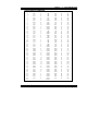
1
USER’S MANUAL ProX-B501 Pentium® M Flex-ATX Motherboard With VGA/Sound/2LAN Prox-B501 M2 Copyright Notice Prox-B501 Pentium® M Flex-ATX Motherboard With VGA/ Sound/ 2LAN OPERATION MANUAL COPYRIGHT NOTICE This operation manual is meant to assist both Embedded Computer manufacturers and end users in installing and setting up the system. The information contained in this document is subject to change without any notice. This manual is copyrighted in May, 2004. You may not reproduce or transmit in any form or by any means, electronic, or mechanical, including photocopying and recording. ACKNOWLEDGEMENTS All trademarks and registered trademarks mentioned herein are the property of their respective owners. CE NOTICE This is a class A product. In a domestic environment this product may cause radio interference in which case the user may be required to take adequate measures. ! Copyright Notice FCC NOTICE This equipment has been tested and found to comply with the limits for a Class A digital device, pursuant to part 15 of the FCC Rules. These limits are designed to provide reasonable protection against harmful interference when the equipment is operated in a commercial environment. This equipment generates, uses, and can radiate radio frequency energy and, if not installed and used in accordance with the instruction manual, may cause harmful interference to radio communications. Operation of this equipment in a residential area is likely to cause harmful interference in which case the user will be required to correct the interference at his own expense. You are cautioned that any change or modifications to the equipment not expressly approve by the party responsible for compliance could void your authority to operate such equipment. ! Contents TABLE OF CONTENTS CHAPTER 1-1 1-2 1-3 CHAPTER 2-1 2-2 2-3 2-4 2-5 2-6 2-7 2-8 2-9 2-10 2-11 2-12 2-13 2-14 2-15 2-16 2-17 2-18 2-19 2-20 2-21 2-22 2-23 2-24 2-25 2-26 2-27 2-28 2-29 ! ! 1 INTRODUCTION About This Manual ........................................................ System Specification ...................................................... Safety Precautions ......................................................... 2 1-2 1-3 1-6 HARDWARE CONFIGURATION Jumper & Connector Quick Reference Table ................ Component Locations .................................................... How to Set the Jumpers ................................................. COM Port Connector ……..…………………………... COM3 RI& Voltage Selection ……………………….. COM4 RI& Voltage Selection ………………………… RS232/422/485(COM2) Selection ............................... Keyboard or PS/2 Mouse Connector .....................….... Reset Connector ............................................................ Hard Disk Drive LED Connector .................................. ATX Power Button ….................................................... External Speaker Connector .......................................... Power Led Connector ……............................................ KeyLock Connector ..………………………………… External SMI Connector ……………………………… Inverter Connector ……………………………………. Clear CMOS Data Selection ………………………… CPU Fan Connector ………………………………….. System Fan Connector ………………………………… VGA Connector …………………..…………………… Hard Disk Drive Connector ........................................... Floppy Disk Drive Connector ....................................... Printer Connector .......................................................... Universal Serial Bus Connector ……………………… IrDA Connector ………………………………………. USB & LAN Connector ……………………………… GigaLAN (LAN2) Enable/Disable Selection ………… Memory Installation ………………………………….. LVDS Connector ……………………………………… 2-2 2-3 2-4 2-6 2-8 2-9 2-10 2-11 2-11 2-11 2-12 2-12 2-12 2-13 2-13 2-13 2-14 2-14 2-15 2-15 2-16 2-18 2-19 2-20 2-20 2-21 2-23 2-24 2-24 Contents ! ! 2-30 2-31 2-32 2-33 2-34 ATX Power Connector ……………………………….. Sound Connector ……………………………….…….. CD Audio-in Connector ………………………………. LVDS Panel Voltage Selection ………………………. LVDS Brightness & Backlight Control Connector …… CHAPTER 3-1 3-2 3-3 3-4 3-5 3-6 3-7 ! SOFTWARE UTILITIES Introduction …………..........................................…....... VGA Driver Utility ……………………………….…… Flash BIOS Update ..............................................…....... LAN Driver Utility …...........................................…...... Sound Driver Utility …………………………………… Intel Chipset Software Installation Utility …..……..….. USB2.0 Software Installation Utility ………………….. CHAPTER 4-1 4-2 4-3 4-4 4-5 4-6 4-7 4-8 4-9 4-10 4-11 4-12 4-13 4-14 4-15 3 4 2-25 2-26 2-27 2-27 2-27 3-2 3-3 3-4 3-6 3-7 3-8 3-9 AWARD BIOS SETUP Introduction ................................................................... Entering Setup ............................................................... The Standard CMOS Features ………............................ The Advanced BIOS Features ....................................... Advanced Chipset Features ........................................... Integrated Peripherals …............................................... Power Management Setup ............................................. PNP/PCI Configuration …............................................. PC Health Status …….................................................... Frequency Control ....................................…………...... Load Fail-Safe Defaults ................................................. Load Optimized Defaults .........................................…. Password Setting ……………………………………… Save & Exit Setup ......................................................... Exit Without Saving ………………………………… 4-2 4-3 4-4 4-8 4-11 4-13 4-18 4-21 4-23 4-24 4-25 4-25 4-26 4-27 4-28 Contents ! ! ! APPENDIX A EXPANSION BUS PCI Bus Pin Assignment ..............................................…......... AGP Bus Pin Assignment ..........................………................... APPENDIX B TECHNICAL SUMMARY Block Diagram ........................................................................... Interrupt Map ............................................................................ RTC & CMOS RAM Map ........................................................ Timer & DMA Channels Map .................................................. I/O & Memory Map ...............................................…................ ! A-2 A-3 B-2 B-3 B-4 B-5 B-6 ! ! ! ! ! ! ! ! ! ! CHAPTER INTRODUCTION! 1 ! This chapter gives you the information for Prox-B501. It also outlines the System specifications. Section includes: z About This Manual z System Specifications z Safety Precautions Experienced users can skip to chapter 2 on page 2-1 for a Quick Start. ! ! Page:1-1 Chapter 1 Introduction 1-1. ABOUT THIS MANUAL ! Thank you for purchasing our Prox-B501 Socket 478 Mainboard enhanced with VGA/Sound/2LAN, which is fully PC / AT compatible. The ProxB501 provides faster processing speed, greater expandability and can handle more tasks than before. This manual is designed to assist you how to install and set up the system. It contains four chapters. The user can apply this manual for configuration according to the following chapters: Chapter 1 Introduction This chapter introduces you to the background of this manual, and the specifications for this system. The final page of this chapter will indicate how to avoid damaging this board. Chapter 2 Hardware Configuration This chapter outlines the component locations and their functions. In the end of this chapter, you will learn how to set jumper and how to configure this card to meet your own needs. Chapter 3 Software Utilities This chapter contains helpful information for proper installations of the VGA utility, LAN utility, Sound utility, and Flash BIOS Update. It also describes the Watchdog-timer configuration. Chapter 4 Award BIOS Setup This chapter indicates you how to set up the BIOS configurations. Appendix A Expansion Bus This Appendix introduces you the expansion bus for AGP BUS and PCI BUS. Appendix B Technical Summary This section gives you the information about the Technical maps. Appendix C Trouble Shooting This section outlines the error messages and offers you the methods to solve the problems. ! Page: 1-2 Prox-B501 USERcS MANUAL Chapter 1 Introduction 1-2. SYSTEM SPECIFICATIONS z CPU (mPGA478): Intel® Pentium® M / Celeron M Type processor in mPGA478 Socket. 1.3~1.8 GHz clock generator. Front Side Bus 400 MHZ. Auto detect voltage regulator. z MEMORY : Supports up to 2GB DDR SDRAM. Two 184-pin DDR DIMM sockets on board. z CACHE : Built-in CPU. z REAL-TIME CLOCK : 256-byte battery backed CMOS RAM. Hardware implementation to indicate century rollover. z BIOS : Phoenix-AwardBIOS for plug & play function. 4/8MB with VGA BIOS. Easy update 512KB flash EEPROM. Support S/IO Setup. z KEYBOARD CONNECTOR : Mini DIN connector. Supports for AT/PS2 keyboard. z MOUSE CONNECTOR : Mini DIN connector. Supports for PS/2 Mouse. z BUS SUPPORT : External 2 PCI, 1 AGP Bus ! Prox-B501 USERcS MANUAL Page: 1-3 Chapter 1 Introduction z DISPLAY : Built-in Intel 855GME/GM, support for CRT, DVO and LVDS. Onboard 15-pin VGA D-SUB connector, support for resolution on SVGA Monitor. z IDE INTERFACE : Two IDE ports support up to four IED devices. Supports Ultra DMA 33/66/100. z FLOPPY DISK DRIVER INTERFACE : Support up to two Floppy Disk Drives, 3.5" and 5.25" (360K / 720K / 1.2M / 1.44M / 2.88M). z USB CONNECTOR : Support up to six USB 2.0 ports. z LAN ADAPTER : Dual ports, Intel® 82562EM PHY & Intel 82540EM (10/100/1000) LAN1: 10BaseT/100 BaseTx Ethernet LAN2: 10/100/1000 BaseT (82540EM) Support wake-on-LAN function. z SERIAL PORT : Four high speed 16550 Compatible UARTs with Send / Receive 16 Byte FIFOs; COM1/3/4:RS-232; COM2: RS-232/422/485 MIDI Compatible Programmable Baud Rate Generator z SOUND : Realtek ALC202A (AC’97 Codec). Fully Compliant AC’97 Analog I/O Component 16-Bit Stereo Full-Duplex Codec Four Analog Line-level Stereo Inputs for Connection. High Quality CD Input with Ground Sense Stereo Line-Level Output Interface: Line-In, Line-Out, Microphone, and CD Audio-In. ! Page: 1-4 Prox-B501 USERcS MANUAL Chapter 1 Introduction z HARDWARE MONITORING FUNCTION : Monitor Voltage, CPU temperature, & Cooling fan. If CPU Temperature is over setting, the buzzer will send out a warming (only under DOS system). z IRDA PORT : 5-pin Infrared port, support IrDA v1.0 SIR protocol z PARALLEL PORT : SPP / ECP / EPP Function. 1 port, bi-directional parallel port. z GREEN FUNCTION : Controlled by hardware and software. z LED INDICATOR : System power Hard Disk access LAN LED indicator z DMA CONTROLLER : 82C37 x 2 z DMA CHANNELS : 7 z INTERRUPT CONTROLLERS : 82C59 x 2 z INTERRUPT LEVELS : 15 z OPERATING TEMPERATURE : 0 to 60qC. z BOARD DIMENSIONS : 228.6mm x 190.5mm, 9” x7.5” z BOARD NET WEIGHT : 490 gram. ! Prox-B501 USERcS MANUAL Page: 1-5 Chapter 1 Introduction 1-3. SAFETY PRECAUTIONS Follow the messages below to avoid your systems from damage: 1. Keep your system away from static electricity on all occasions. 2. Prevent electric shock. Don‘t touch any components of this card when the card is power-on. Always disconnect power when the system is not in use. 3. Disconnect power when you change any hardware devices. For instance, when you connect a jumper or install any cards, a surge of power may damage the electronic components or the whole system. ! Page: 1-6 Prox-B501 USERcS MANUAL HARDWARE CONFIGURATION CHAPTER 2 ** QUICK START ** Helpful information describes the jumper & connector settings, and component locations. Section includes: z Jumper & Connector Quick Reference Table z Component Locations z Configuration and Jumper settings z Connector’s Pin Assignments Page 2-1 Chapter 2 Hardware Configuration 2-1. JUMPER & CONNECTOR QUICK REFERENCE TABLE COM Port Connector ....................…..................……… ………………………………….. COM3 Port RI/Voltage Selection ……………………. COM4 Port RI/Voltage Selection …………………….. RS232/422/485 (COM2) Selection .....................……… Keyboard/Mouse Connector ..........….....……………… Reset Connector .........................…....................………. Hard Disk Drive LED Connector .......................………. ATX Power Button …………………………………….. External Speaker Connector ....…........................……… Power LED Connector …………….…...............……… KeyLock Connector ……………………………………. External SMI Connector ……………………………….. Inverter Connector …………………………………….. Clear CMOS Data Selection …………………………… CPU Fan Connector …………………………………… System Fan Connector …………………………………. VGA Connector …................……..…………………… Hard Disk Drive Connector …..............…….........……. Floppy Disk Drive Connector ….............…….......……. Printer Connector …........................…...…….........…… Universal Serial Bus Connector …........................…..… IrDA Connector ……………………………………….. USB&LAN Connector …....................................…… GigaLAN (LAN2) Enable/Disable Selection ………….. ATX Power Connector ………………………………… Memory Installation ..................................…......……… LVDS Connector ……………………………………… Sound Connector ………………………….…………… CD Audio-In Connector ……………………………….. LVDS Voltage Selection ……………………………… LVDS Brightness & Backlight Control Connector …… Reserved Pin …………………………………………… Page: 2-2 COM1, COM2 COM3, COM4 JP1 JP3 JP5 JKBMS1 JPANEL (13,15) JPANEL (9,11) JPANEL (14,16) JPANEL (1,3,5,7) JPANEL (8,10,12) JPANEL (17,18) JPANEL (2, 4) J3 JP12 JCFAN1 JSFAN1 VGA IDE1, IDE2 FDD1 LPT1 JUSB1 IRDA1, JPANEL (21-24) J1, J2 JP2 PW1 DIMM1, DIMM2 J4 JAUDIO1 JCDIN1 JP9 J5 J7, JP8, Prox-B501 USERcS MANUAL Chapter 2 Hardware Configuration 2-2. COMPONENT LOCATIONS Prox-B501 Connector, Jumper and Component locations Prox-B501 USERcS MANUAL Page: 2-3 Chapter 2 Hardware Configuration 2-3. HOW TO SET THE JUMPERS You can configure your board by setting jumpers. Jumper is consists of two or three metal pins with a plastic base mounted on the card, and by using a small plastic "cap", Also known as the jumper cap (with a metal contact inside), you are able to connect the pins. So you can set-up your hardware configuration by "open" or "close" pins. The jumper can be combined into sets that called jumper blocks. When the jumpers are all in the block, you have to put them together to set up the hardware configuration. The figure below shows how this looks like. JUMPERS AND CAPS If a jumper has three pins (for examples, labelled PIN1, PIN2, and PIN3), You can connect PIN1 & PIN2 to create one setting and shorting. You can either connect PIN2 & PIN3 to create another setting. The same jumper diagrams are applied all through this manual. The figure below shows what the manual diagrams look and what they represent. Page: 2-4 Prox-B501 USERcS MANUAL Chapter 2 Hardware Configuration JUMPER DIAGRAMS Jumper Cap looks like this 2 pin Jumper looks like this 3 pin Jumper looks like this Jumper Block looks like this JUMPER SETTINGS 2 pin Jumper close(enabled) Looks like this 1 1 3 pin Jumper 2-3 pin close(enabled) Looks like this 1 1 Jumper Block 1-2 pin close(enabled) Looks like this 1 2 Prox-B501 USERcS MANUAL 1 2 Page: 2-5 Chapter 2 Hardware Configuration 2-4. COM PORT CONNECTOR COM1 : COM1 Connector COM1 is fixed as RS-232. The pin assignment is as follows : PIN 1 2 3 4 5 6 7 8 9 10 COM1 ASSIGNMENT DCD RX TX DTR GND DSR RTS CTS RI NC COM2 : COM2 Connector The COM2 is selectable as RS-232/422/485. The pin assignment is as follows : PIN 1 2 3 4 5 6 7 8 9 10 Page: 2-6 ASSIGNMENT RS-232 RS-422 DCD TXRX TX+ TX RX+ DTR RXGND GND DSR RTSRTS RTS+ CTS CTS+ RI CTSNC NC RS-485 TXTX+ RX+ RXGND NC NC NC NC NC 6 10 1 5 COM2 Prox-B501 USERcS MANUAL Chapter 2 Hardware Configuration COM3 : COM3 Connector COM3 is fixed as RS-232. The pin assignment is as follows : PIN 1 2 3 4 5 6 7 8 9 10 ASSIGNMENT DCD RX TX DTR GND DSR RTS CTS RI-V NC COM4 : COM4 Connector COM4 is fixed as RS-232. The pin assignment is as follows : PIN 1 2 3 4 5 6 7 8 9 10 ASSIGNMENT DCD RX TX DTR GND DSR RTS CTS RI-V NC Prox-B501 USERcS MANUAL 5 10 1 6 COM3 5 1 10 6 COM4 Page: 2-7 Chapter 2 Hardware Configuration 2-5. COM3 RI & VOLTAGE SELECTION JP1 : COM3 RI & Voltage Selection The selections are as follows: SELECTION JUMPER SETTINGS RI 1-2 +12V 3-4 +5V 5-6 JUMPER ILLUSTRATION ***Manufacturing Default – RI. Page: 2-8 Prox-B501 USERcS MANUAL Chapter 2 Hardware Configuration 2-6. COM4 RI & VOLTAGE SELECTION JP3 : COM4 RI & Voltage Selection The selections are as follows: SELECTION JUMPER SETTINGS RI 1-2 +12V 3-4 +5V 5-6 JUMPER ILLUSTRATION ***Manufacturing Default – RI. Prox-B501 USERcS MANUAL Page: 2-9 Chapter 2 Hardware Configuration 2-7. RS232/422/485 (COM2) SELECTION JP5 : RS-232/422/485 (COM2) Selection This connector is used to set the COM2 function. The jumper settings are as follows : COM 2 Function Jumper Settings (pin closed) RS-232 Open RS-422 1-2, 5-6, 7-8 9-10, 11-12, 13-14 15-16, 17-18, 19-20 RS-485 1-3, 4-6, 7-8, 9-10 11-12, 13-14, 15-16 17-18, 19-20 Jumper Illustrations *** Manufactory default --- RS-232. Page: 2-10 Prox-B501 USERcS MANUAL Chapter 2 Hardware Configuration 2-8. KEYBOARD OR PS/2 MOUSE CONNECTOR JKBMS1 : Keyboard or PS/2 Mouse Connector DIN connector can support keyboard, Y-cable, or PS/2 Mouse, user may select the right device to used on “Keyboard or PS/2 Mouse Selection”. The pin assignments are as follows : PIN 1 2 3 4 5 6 ASSIGNMENT Keyboard PS/2 Mouse KBDATA MSDATA MSDATA MSDATA GND GND +5V +5V KBCLK MSCLK MSCLK MSCLK 6 5 3 4 2 1 9 8 7 JKBMS1 2-9. RESET CONNECTOR JPAENL (13,15) : Reset Connector. The pin assignment is as follows : PIN 13 15 1 JPANEL1 ASSIGNMENT GND RST_SW 2-10. HARD DISK DRIVE LED CONNECTOR JPAENL (9,11) : Hard Disk Drive LED Connector The pin assignment is as follows : PIN 9 11 ASSIGNMENT +5V HD_LED Prox-B501 USERcS MANUAL 1 JPANEL1 Page: 2-11 Chapter 2 Hardware Configuration 2-11. ATX POWER BUTTON JPANEL (14,16) : ATX Power Button The pin assignment is as follows : PIN 14 16 1 JPANEL1 ASSIGNMENT PWR_BN1 PWR_BN2 2-12. EXTERNAL SPEAKER CONNECTOR JPANEL (1,3,5,7) : External Speaker Connector The pin assignment is as follows : SPEAKER 1 PIN 1 3 5 7 JPANEL1 ASSIGNMENT +5V NC NC SPEAKER SIGNAL 2-13. POWER LED CONNECTOR JPAENL (8,10,12) : Power LED Connector The pin assignment is as follows: PIN 8 10 12 Page: 2-12 ASSIGNMENT PW_LED PW_LED GND 1 JPANEL1 Prox-B501 USERcS MANUAL Chapter 2 Hardware Configuration 2-14. KEYLOCK CONNECTOR JPAENL (17,18) : Keylock Connector The pin assignment is as follows: 1 PIN 17 18 JPANEL1 ASSIGNMENT KEYLOCK GND 2-15. EXTERNAL SMI CONNECTOR JPAENL (2,4) : External SMI Connector The pin assignment is as follows: PIN 2 4 ASSIGNMENT 5VSB GND 1 JPANEL1 2-16. INVERTER CONNECTOR J3 : Inverter Connector The pin assignment is as follows: PIN 1 2 3 4 5 ASSIGNMENT +12V GND +5V GND ENABKL (Inverter backlight ON/OFF control signal) Prox-B501 USERcS MANUAL Page: 2-13 Chapter 2 Hardware Configuration 2-17. CLEAR CMOS DATA SELECTION JP12 : Clear CMOS Data Selection The selections are as follows : FUNCTION JUMPER SETTING (pin closed) Normal 1-2 Clear CMOS 2-3 JUMPER ILLUSTRATION *** Manufacturing Default is set as Normal. Note: To clear CMOS data, user must power-off the computer and set the jumper to “Clear CMOS” as illustrated above. After five to six seconds, set the jumper back to “Normal” and power-on the computer. 2-18. CPU FAN CONNECTOR JCFAN1 : CPU Fan connector The pin assignment is as follows: PIN 1 2 3 Page: 2-14 ASSIGNMENT GND +12V FAN1 Prox-B501 USERcS MANUAL Chapter 2 Hardware Configuration 2-19. SYSTEM FAN CONNECTOR JSFAN1 : System Fan connector The pin assignment is as follows: PIN 1 2 3 ASSIGNMENT GND +12V FAN0 2-20. VGA CONNECTOR VGA : VGA CRT Connector The pin assignments are as follows: PIN 1 2 3 4 5 6 7 8 9 10 11 12 13 14 15 ASSIGNMENT RED GREEN BLUE NC GND GND GND GND VCC GND NC VGA DDA HSYNC VSYNC VGA DDC CLK Prox-B501 USERcS MANUAL 15 10 11 6 1 5 VGA Page: 2-15 Chapter 2 Hardware Configuration 2-21. HARD DISK DRIVE CONNECTOR IDE1: Hard Disk Drive Connector The Prox-B501 possesses two HDD connectors, IDE1 and IDE2. The pin assignments are as follows: PIN 1 3 5 7 9 11 13 15 17 19 21 23 25 27 29 31 33 35 37 39 Page: 2-16 ASSIGNMENT IDERST PDD7 PDD6 PDD5 PDD4 PDD3 PDD2 PDD1 PDD0 GND PDREQ PDIOW# PDIOR# PIORDY PDDACK# IRQ14 PDA1 PDA0 PDCS#1 IDEACTP# PIN 2 4 6 8 10 12 14 16 18 20 22 24 26 28 30 32 34 36 38 40 ASSIGNMENT GND PDD8 PDD9 PDD10 PDD11 PDD12 PDD13 PDD14 PDD15 NC GND GND GND PULL LOW GND NC P66 DETECT PDA2 PDCS#3 GND Prox-B501 USERcS MANUAL Chapter 2 Hardware Configuration IDE2: Hard Disk Drive Connector The pin assignments are as follows: PIN 1 3 5 7 9 11 13 15 17 19 21 23 25 27 29 31 33 35 37 39 ASSIGNMENT IDERST SDD7 SDD6 SDD5 SDD4 SDD3 SDD2 SDD1 SDD0 GND SDREQ SDIOW# SDIOR# SIORDY SDDACK# IRQ15 SDA1 SDA0 SDCS#1 IDEACTS# Prox-B501 USERcS MANUAL PIN 2 4 6 8 10 12 14 16 18 20 22 24 26 28 30 32 34 36 38 40 ASSIGNMENT GND SDD8 SDD9 SDD10 SDD11 SDD12 SDD13 SDD14 SDD15 NC GND GND GND PULL LOW GND NC S66 DETECT SDA2 SDCS#3 GND Page: 2-17 Chapter 2 Hardware Configuration 2-22. FLOPPY DISK DRIVE CONNECTOR FDD1 : Floppy Disk Drive Connector You can use a 34-pin daisy-chain cable to connect two-FDDs. On one end of this cable is a 34-pin flat cable to attach the FDD on the board, and the other side is attaches two FDDs. The pin assignments are as follows : 2 34 1 33 FDD1 PIN 1 3 5 7 9 11 13 15 17 19 21 23 25 27 29 31 33 Page: 2-18 ASSIGNMENT GND GND GND GND GND GND GND GND GND GND GND GND GND GND NC GND NC PIN 2 4 6 8 10 12 14 16 18 20 22 24 26 28 30 32 34 ASSIGNMENT RWC# NC DS1# INDEX MOA# DSB# DSA# MOB# DIR# STEP# WD# WE# TRK0# WP# RDATA# HEAD# DSKCHG Prox-B501 USERcS MANUAL Chapter 2 Hardware Configuration 2-23. PRINTER CONNECTOR LPT : Printer Connector As to link the Printer to the card, you need a cable to connect both DB25 connector and parallel port. The pin assignments are as follows : LPT1 PIN 1 2 3 4 5 6 7 8 9 10 11 12 13 ASSIGNMENT STB PDR0 PDR1 PDR2 PDR3 PDR4 PDR5 PDR6 PDR7 ACK# BUSY PE SLCT Prox-B501 USERcS MANUAL PIN 14 15 16 17 18 19 20 21 22 23 24 25 26 ASSIGNMENT AFD# ERROR# PAR_INIT# SLIN# GND GND GND GND GND GND GND GND NC Page: 2-19 Chapter 2 Hardware Configuration 2-24. UNIVERSAL SERIAL BUS CONNECTOR JUSB1: Universal Serial Bus Connector The pin assignments are as follows: PIN 1 2 3 4 5 6 7 8 9 10 ASSIGNMENT +5V +5V USB0 USB1 USB0+ USB1+ GND GND NC NC 10 9 2 1 JUSB1 2-25. IRDA CONNECTOR IRDA1: IrDA (Infrared) Connector The pin assignments are as follows: PIN 1 2 3 4 5 Page: 2-20 ASSIGNMENT +5V NC IRRX GND IRTX 1 IRDA1 Prox-B501 USERcS MANUAL Chapter 2 Hardware Configuration JPAENL (21-24) : IrDA Connector The pin assignment is as follows: PIN 21 22 23 24 ASSIGNMENT +5V GND IRTX2 IRRX2 1 JPANEL1 2-26. USB&LAN CONNECTOR J1: USB & LAN Connector The pin assignments are as follows: LAN: PIN ASSIGNMENT 1 TX+ 2 TX3 RX+ 4 ISOLATED GND 5 ISOLATED GND 6 RX7 ISOLATED GND 8 ISOLATED GND 11 YLED+ 12 YLED13 OLED+ 14 OLED The green LED detect power link, and the Yellow LED is used to detect data active transfer signal. Prox-B501 USERcS MANUAL 1 10 J1 Page: 2-21 Chapter 2 Hardware Configuration USB: PIN A1 A2 A3 A4 B1 B2 B3 B4 ASSIGNMENT +5V USB0USB0+ GND +5V USB1USB1+ GND J2: USB & LAN Connector The pin assignments are as follows: LAN: PIN ASSIGNMENT 1 TX+ 2 TX3 RX+ 4 ISOLATED GND 5 ISOLATED GND 6 RX7 ISOLATED GND 8 ISOLATED GND 11 YLED+ 12 YLED13 OLED+ 14 OLED The green LED detect power link, and the Yellow LED is used to detect data active transfer signal. Page: 2-22 1 10 J2 Prox-B501 USERcS MANUAL Chapter USB: PIN A1 A2 A3 A4 B1 B2 B3 B4 2 Hardware Configuration ASSIGNMENT +5V USB0USB0+ GND +5V USB1USB1+ GND 2-27. GIGALAN (LAN2) ENABLE/DISABLE SELECTION JP2 : GigaLAN (LAN2) Enable/Disable Selection. The selections are as follows: FUNCTION JUMPER SETTING (pin closed) Enable 1-2 Disable 2-3 Prox-B501 USERcS MANUAL JUMPER ILLUSTRATION Page: 2-23 Chapter 2 Hardware Configuration 2-28. MEMORY INSTALLATION Prox-B501 CPU Card can support up to 2GB in two DIMM sockets. DRAM BANK CONFIGURATION DIMM 1 128MB 256MB 512MB 1GB DIMM 2 128MB 256MB 512MB 1GB TOTAL MEMORY 256MB 512GB 1GB 2GB 2-29. LVDS CONNECTOR J4 : LVDS Connector. The pin assignments are as follows: PIN 1 3 5 7 9 11 13 15 17 19 21 23 25 27 29 Page: 2-24 ASSIGNMENT LCD_VCC ZCM GND Z2P Z1M Z3P Z0P GND YCM Y2P GND Y1M Y0P Y3P LCD_VCC PIN 2 4 6 8 10 12 14 16 18 20 22 24 26 28 30 ASSIGNMENT GND ZCP Z2M GND Z1P Z3M Z0M YCP GND Y2M Y1P GND Y0M Y3M LCD_VCC J4 1 Prox-B501 USERcS MANUAL Chapter 2 Hardware Configuration 2-30. ATX POWER CONNECTOR PW1 : ATX Power Connector The pin assignments are as follows: PIN 1 2 3 4 5 6 7 8 9 10 11 12 13 14 15 16 17 18 19 20 ASSIGNMENT 3.3V 3.3V GND 5V GND 5V GND POK 5VSB 12V 3.3V -12V GND PSON GND GND GND -5V 5V 5V Prox-B501 USERcS MANUAL Page: 2-25 Chapter 2 Hardware Configuration 2-31. SOUND CONNECTOR JAUDIO1 : Sound Connector, including Line-In, Line-Out & Mic. Also can support only MIC connector. The pin assignments are as follows : 32 33 34 35 22 23 24 25 2 3 1 4 5 Line-In PIN ASSIGNMENT 32 LINE_L 33 GND 34 GND 35 LINE_R Line-In Line-Out PIN ASSIGNMENT 22 SPK-L 23 NC 24 NC 25 SPK-R Mic-In PIN 1 2 3 4 Page: 2-26 Line-Out Mic-In JAUDIO1 ASSIGNMENT GND MIC_IN GND NC Prox-B501 USERcS MANUAL Chapter 2 Hardware Configuration 2-32. CD AUDIO-IN CONNECTOR 1 JCDIN1 : CD Audio-In Connector The pin assignments are as follows: PIN 1 2 3 4 JCDIN1 ASSIGNMENT CD L GND GND CD R 2-33. LVDS PANEL VOLTAGE SELECTION JP9 : LVDS Panel Voltage Selection. The selections are as follows: SELECTION LVDS_VCC3 LVDS_VCC5 JUMPER SETTING JUMPER ILLUSTRATION 1-3 2-4 3-5 4-6 2-34. LVDS BRIGHTNESS & BACKLIGHT CONTROL CONNECTOR J5 : LVDS Brightness and Backlight Control Connector The pin assignment is as follows: PIN 1 2 ASSIGNMENT Brightness Control LCD Back Light Enable Prox-B501 USERcS MANUAL 1 J5 Page: 2-27 SOFTWARE UTILITIES CHAPTER 3 This chapter comprises the detailed information of VGA driver, LAN driver, and Flash BIOS update. It also describes how to install the watchdog timer configuration. Section includes: z VGA Driver Utility z Flash BIOS Update z LAN Driver Utility z Sound Driver Utility z Intel® Chipset Software Installation Utility z USB2.0 Chipset Software Installation Utility Page: 3-1 Chapter 3 Software Configuration 3-1. INTRODUCTION Enclosed with our Prox-B501 package is our driver utility, which may comes in a form of a CD ROM disc or floppy diskettes. For CD ROM disc user, you will only need some of the files contained in the CD ROM disc, please kindly refer to the following chart: Filename (Assume that CD ROM drive is D:) D:\VGA Purpose Intel 855GME For VGA driver installation D:\AWDFLASH For BIOS update utility D:\LAN For LAN Driver installation D:\SOUND Realtel ALC202A AC97 For Sound driver installation D:\UTILITY Intel® Chipset Software Installation Utility For Win 98SE,ME, 2000, XP D:\USB 2.0 USB 2.0 Software Installation Utility For Win 98SE, 2000, ME, XP User should remember to install the Utility right after the OS fully installed. Page:3-2 Prox-B501 USERcS MANUAL Chapter 3 Software Configuration 3-2. VGA DRIVER UTILITY The VGA interface embedded with our Prox-B501 can support a wide range of display. You can display CRT, LVDS simultaneously with the same mode. 1. Win 98/ME program 2. Win NT 4.0 program 3. Win 2000 program 4. Win XP program 5. Linux 3-2-1. Installation of VGA Driver: To install the VGA Driver, simply follow the following steps: 1. 2. 3. 4. 5. Place insert the Utility Disk into Floppy Disk Drive A/B or CD ROM drive. Under Windows 9X/NT4.0/2000/XP system, go to the directory where VGA driver is located. Click Setup.exe file for VGA driver installation. Follow the instructions on the screen to complete the installation. Once installation is completed, shut down the system and restart in order for the changes to take effect. Prox-B501 USERcS MANUAL Page:3-3 Chapter 3 Software Configuration 3-3. FLASH BIOS UPDATE 3-3-1. System BIOS Update: Users of Prox-B501 can use the program “Awdflash.exe” contained in the Utility Disk for system BIOS and VGA BIOS update. 3-3-2. To update VGA BIOS for LCD Flat Panel Display: As Prox-B501 user, you have to update the VGA BIOS for your specific LCD flat panel you are going to use. For doing this, you need two files. One is the “Awdflash.exe” file and the other is the VGA BIOS for ATI Rage Mobility M6 file for LCD panel display. Both file must be provided by the vendor or manufacturer. When you get these two files ready, follow the following steps for updating your VGA BIOS: 1. 2. 3. 4. Install “Awdflash.exe” from Utility Disk to Drive C. Insert the VGA BIOS file you have obtained from the vendor. Type the path to Awdflash.exe and execute the VGA BIOS update with file H15bxxxx.bin C:\UTIL\AWDFLASH>AWDFLASH H15bxxxx.bin The screen will display as the table fount on the next page: FLASH MEMORY WRITER v7.XX (C) Award Software 2001 All Rights Reserved Flash Type – SST 49LF004A /3.3V File Name to Program: H20bxxxx.bin Checksum: XXXXX Error Message: Page:3-4 Do You Want To Save BIOS (Y/N) Prox-B501 USERcS MANUAL Chapter 3 Software Configuration If you want to save up the original BIOS, enter "Y" and press < Enter >. If you choose "N", the following table will appear on screen. FLASH MEMORY WRITER v7.XX (C) Award Software 2001 All Rights Reserved Flash Type – SST 49LF004A /3.3V File Name to Program: H20bxxxx.bin Checksum: XXXXX Error Message : Are You Sure To Program (Y/N) Select "Y", and the BIOS will be renewed. When you are refreshing the BIOS, do not turn off or reset the system, or you will damage the BIOS. After you have completed all the programming, the screen displays the table below: FLASH MEMORY WRITER v7.XX (C) Award Software 2001 All Rights Reserved Flash Type – SST 49LF004A /3.3V File Name to Program: H20bxxxx.bin Checksum: XXXXX Reset System or Power off to accomplish update process! F1: Reset F10: Exit Please reset or power off the system, and then the Flash BIOS is fully implemented. Prox-B501 USERcS MANUAL Page:3-5 Chapter 3 Software Configuration 3-4. LAN DRIVER UTILITY 3-4-1. Introduction Prox-B501 is enhanced with LAN function that can support various network adapters. Installation programs for LAN drivers are listed as follows: 1. Win 98/ME program 2. Win 2000/XP program 3. Win NT 4.0 program 4. Linux program 5. Netware program 6. Unixware 7.x For more details on Installation procedure, please refer to Readme.txt file found on LAN DRIVER UTILITY. Page:3-6 Prox-B501 USERcS MANUAL Chapter 3 Software Configuration 3-5. SOUND DRIVER UTILITY 3-5-1. Introduction The Realtek ALC202A sound function enhanced in this system is fully compatible with Windows 98, Windows 98SE, Windows NT 4.0, Windows 2000, Windows ME and Windows XP. Below, you will find the content of the Sound driver : 1. Win 98/ME program 2. Win NT 4.0 program 3. Win 2000/XP program 4. Linux program 3-5-2. Installation Procedure for Windows 9x/NT/2000/XP 1. 2. 3. 4. 5. From the task bar, click on Start, and then Run. In the Run dialog box, type D:\Sound\path\setup, where “D:\Sound\pathname” refers to the full path to the source files. Click on the OK button or press the ENTER key. Click on the “Next” and OK prompts as they appear. Reboot the system to complete the driver installation. Prox-B501 USERcS MANUAL Page:3-7 Chapter 3 Software Configuration 3-6. INTEL® CHIPSET SOFTWARE INSTALLATION UTILITY 3-6-1. Introduction The Intel® Chipset Software Installation Utility installs to the target system the Windows* INF files that outline to the operating system how the chipset components will be configured. This is needed for the proper functioning of the following features: - Core PCI and ISAPNP Services AGP Support IDE/ATA33/ATA66/ATA100 Storage Support USB Support Identification of Intel® Chipset Components in Device Manager 3-6-2. Installation of Utility for Windows 98SE/ME/2000/XP The Utility Pack is to be installed only for Windows 98SE, Windows ME, Windows 2000 and XP program. It should be installed right after the OS installation, kindly follow the following steps: 1. 2. 3. 4. 5. Page:3-8 Place insert the Utility Disk into Floppy Disk Drive A/B or CD ROM drive. Under Windows 98SE/ME/2000/XP system, go to the directory where Utility Disc is located. Click Setup.exe file for utility installation. Follow the instructions on the screen to complete the installation. Once installation is completed, shut down the system and restart in order for the changes to take effect. Prox-B501 USERcS MANUAL Chapter 3 Software Configuration 3-7. USB2.0 SOFTWARE INSTALLATION UTILITY 3-7-1. Installation of Utility for Windows 98SE/ 2000/XP Intel USB 2.0 Enhanced Host Controller driver can only be used on Windows 98SE, Windows 2000 and Windows XP on Intel Desktop boards. It should be installed right after the OS installation, kindly follow the following steps: 1. 2. 3. 4. 5. 6. 7. 8. 9. Place insert the Utility Disk into Floppy Disk Drive A/B or CD ROM drive. Under Windows 98SE, 2000, and XP system, go to the directory where Utility Disc is located. Start the “System” wizard in control panel. (Click Start/Settings/Control Panel). Select “Hardware” and click “Device Manager ” button. Double Click “USB Root Hub”. Select “Driver”. Click “Install” to install the driver. Follow the instructions on the screen to complete the installation. Click “Finish” after the driver installation is complete. Prox-B501 USERcS MANUAL Page:3-9 CHAPTER AWARD BIOS SETUP 4 This chapter shows how to set up the Award BIOS. Section includes: z Introduction z Entering Setup z The Standard CMOS Features z The Advanced BIOS Features z The Advanced Chipset Features z Integrated Peripherals z Power Management Setup z PNP/PCI Configuration z PC Health Status z Frequency Control z Load Fail-Safe Defaults z Load Optimized Defaults z Password Setting z Save and Exit Setup z Exit Without Saving Page: 4-1 Chapter 4 Award BIOS Setup 4-1. INTRODUCTION This chapter will show you the function of the BIOS in managing the features of your system. The Prox-B501 Pentium M Flex-ATX Motherboard is equipped with the BIOS for system chipset from Award Software Inc. This page briefly explains the function of the BIOS in managing the special features of your system. The following pages describe how to use the BIOS for system chipset Setup menu. Your application programs (such as word processing, spreadsheets, and games) rely on an operating system such as DOS or OS/2 to manage such things as keyboard, monitor, disk drives, and memory. The operating system relies on the BIOS (Basic Input and Output system), a program stored on a ROM (Read-only Memory) chip, to initialize and configure your computer's hardware. As the interface between the hardware and the operating system, the BIOS enables you to make basic changes to your system's hardware without having to write a new operating system. The following diagram illustrates the interlocking relationships between the system hardware, BIOS, operating system, and application program: Page: 4-2 Prox-B501 USERcS MANUAL Chapter 4 Award BIOS Setup 4-2. ENTERING SETUP When the system is powered on, the BIOS will enter the Power-On Self Test (POST) routines and the following message will appear on the lower screen: PRESS <DEL> TO ENTER SETUP, ESC TO SKIP MEMORY TEST As long as this message is present on the screen you may press the <Del> key (the one that shares the decimal point at the bottom of the number keypad) to access the Setup program. In a moment, the main menu of the Award SETUP program will appear on the screen: Phoenix - AwardBIOS CMOS Setup Utility ŹStandard CMOS Features ŹFrequency Control ŹAdvanced BIOS Features Load Fail-Safe Defaults ŹAdvanced Chipset Features Load Optimized Defaults ŹIntegrated Peripherals Set Supervisor Password ŹPower Management Setup Set User Password ŹPnP/PCI Configurations Save & Exit Setup ŹPC Health Status Exit Without Saving Esc : Quit F10 : Save & Exit Setup npom : Select Item Time, Date, Hard Disk Type .… Setup program initial screen You may use the cursor the up/down keys to highlight the individual menu items. As you highlight each item, a brief description of the highlighted selection will appear at the bottom of the screen. Prox-B501 USERcS MANUAL Page: 4-3 Chapter 4 Award BIOS Setup 4-3. THE STANDARD CMOS FEATURES Highlight theňSTANDARD CMOS FEATURESʼnand press the <ENTER> key and the screen will display the following table: Phoenix - AwardBIOS CMOS Setup Utility Standard CMOS Features Date (mm:dd:yy) Time (hh:mm:ss) Wed, May 26 2004 15 : 5 : 24 IDE Primary Master IDE Primary Slave IDE Secondary Master IDE Secondary Slave [ None] [ None] [ None] [ None] Drive A Drive B [1.44M, 3.5 in.] [None] Video Halt On [EGA/VGA] [All, But Keyboard] Base Memory Extended Memory Total Memory 640K 490496K 491520K Item Help Menu Level Ź ٿ ٿ ٿ ٿ npom: Move Enter: Select F5: Previous Values +/-/PU/PD:Value Change the internal clock. F10:Save F6: Fail-Safe Defaults ESC:Exit F1:General Help F7:Optimized Defaults CMOS Setup screen In the above Setup Menu, use the arrow keys to highlight the item and then use the <PgUp> or <PgDn> keys to select the value you want in each item. Date: < Month >, < Date > and <Year >. Ranges for each value are in the CMOS Setup Screen, and the week-day will skip automatically. Time: < Hour >, < Minute >, and < Second >. Use 24 hour clock format, i.e., for PM numbers, add 12 to the hour. For example: 4: 30 P.M. You should enter the time as 16:30:00. Page: 4-4 Prox-B501 USERcS MANUAL Chapter 4 Award BIOS Setup IDE Primary Master / Slave: IDE Secondary Master / Slave: The BIOS can automatically detect the specifications and optimal operating mode of almost all IDE hard drives. When you select type AUTO for a hard drive, the BIOS detect its specifications during POST, every time system boots. If you do not want to select drive type AUTO, other methods of selecting drive type are available: 1. Match the specifications of your installed IDE hard drive(s) with the preprogrammed values for hard drive types 1 through 45. 2. Select USER and enter values into each drive parameter field. 3. Use the IDE HDD AUTO DETECTION function in Setup. Here is a brief explanation of drive specifications: Type: The BIOS contains a table of pre-defined drive types. Each defined drive type has a specified number of cylinders, number of heads, write precompensation factor, landing zone, and number of sectors. Drives whose specifications do not accommodate any predefine type are classified as type USER. x Size: Disk drive capacity (approximate). Note that this size is usually greater than the size of a formatted disk given by a disk-checking program. x Cyls: number of cylinders. x Head: number of heads. x Precomp: write precompensation cylinders. x Landz: landing zone. x Sector: number of sectors. x Mode: Auto, Normal, Large or LBA. Auto: The BIOS automatically determines the optimal mode. Normal: Maximum number of cylinders, heads, sectors supported are 1024, 16 and 63. Large: For drives that do not support LBA and have more than 1024 cylinders. Prox-B501 USERcS MANUAL Page: 4-5 Chapter 4 Award BIOS Setup LBA (Logical Block Addressing): During drive accesses, the IDE controller transforms the data address described by sector, head and cylinder number into a physical block address, significantly improving data transfer rates. For drives greater than 1024 cylinders. DRIVE A AND DRIVE B: Select the type of floppy disk drive installed in your system. The available options are 360KB 5.25in, 1.2KB 5.25in, 720KB 3.5in, 1.44MB 3.5in, 2.88MB 3.5in and None. VIDEO: This category selects the type of video adapter used for the primary system monitor. Although secondary monitors are supported, you do not have to select the type in Setup. Available Options are as follows: EGA/VGA Enhanced Graphics Adapter/Video Graphics Array. For EGA, VGA, SEGA, SVGA or PGA monitor adapters. CGA 40 Color Graphics Adapter, power up in 40 column mode. CGA 80 Color Graphics Adapter, power up in 80 column mode. MONO Monochrome adapter, includes high resolution monochrome adapters. HALT ON: This category allows user to choose whether the computer will stop if an error is detected during power up. Available options are “All errors”, “No errors”, “All, But keyboard”, “All, But Diskette”, and “All But Disk/Key”. BASE MEMORY: Displays the amount of conventional memory detected during boot up. EXTENDED MEMORY: Displays the amount of extended memory detected during boot up. TOTAL MEMORY: Displays the total memory available in the system. Page: 4-6 Prox-B501 USERcS MANUAL Chapter 4 Award BIOS Setup HARD DISK ATTRIBUTES: Type 1 2 3 4 5 6 7 8 9 10 11 12 13 14 15 16 17 18 19 20 21 22 23 24 25 26 27 28 29 30 31 32 33 34 35 36 37 38 39 40 41 42 43 44 45 47 Cylinders 306 615 615 940 940 615 642 733 900 820 855 855 306 733 000 612 977 977 1024 733 733 733 306 977 1024 1224 1224 1224 1024 1024 918 925 1024 1024 1024 1024 1024 1024 918 820 1024 1024 809 809 776 Heads 4 4 6 8 6 4 8 5 15 3 5 7 8 7 0 4 5 7 7 5 7 5 4 5 9 7 11 15 8 11 11 9 10 12 13 14 2 16 15 6 5 5 6 6 8 V-P comp 128 300 300 512 512 65535 256 65535 65535 65535 65535 65535 128 65535 0000 0000 300 65535 512 300 300 300 0000 65535 65535 65535 65535 65535 65535 65535 65535 65535 65535 65535 65535 65535 65535 65535 65535 65535 65535 65535 65535 65535 65335 AUTO LZone 305 615 615 940 940 615 511 733 901 820 855 855 319 733 000 663 977 977 1023 732 732 733 336 976 1023 1223 1223 1223 1023 1023 1023 926 1023 1023 1023 1023 1023 1023 1023 820 1023 1023 852 852 775 Sect 17 17 17 17 17 17 17 17 17 17 17 17 17 17 00 17 17 17 17 17 17 17 17 17 17 17 17 17 17 17 17 17 17 17 17 17 17 17 17 17 17 26 17 26 33 Capacity 10 20 30 62 46 20 30 30 112 20 35 49 20 42 00 20 40 56 59 30 42 30 10 40 76 71 111 152 68 93 83 69 85 102 110 119 17 136 114 40 42 65 40 61 100 Award Hard Disk Type Table Prox-B501 USERcS MANUAL Page: 4-7 Chapter 4 Award BIOS Setup 4-4. THE ADVANCED BIOS FEATURES Choose theňADVANCED BIOS FEATURESʼnin the main menu, the screen shown as below. Phoenix - AwardBIOS CMOS Setup Utility Advanced BIOS Features Virus Warning CPU L1 & L2 Cache Quick Power On Self Test First Boot Device Second Boot Device Boot Up Floppy Seek Boot Up NumLock Status Typematic Rate Setting x Typematic Rate (Chars/Sec) x Typematic Delay (Msec) Security Option OS Select For DRAM > 64MB npom: Move Enter: Select F5: Previous Values [Disabled] [Enabled] [Enabled] [Floppy] [HDD-0] [Enabled] [On] [Disabled] 6 250 [Setup] [Non-OS2] +/-/PU/PD:Value Item Help Menu Level Ź Allows you to choose the VIRUS warming feature for IDE Hard Disk boot sector protection. If this function is enabled and someone attempt to write data into this area, BIOS will show a warning message on screen and alarm beep F10:Save F6: Fail-Safe Defaults ESC:Exit F1:General Help F7:Optimized Defaults BIOS Features Setup Screen The “BIOS FEATURES SETUP” allow you to configure your system for basic operation. The user can select the system’s default speed, boot-up sequence, keyboard operation, shadowing and security. A brief introduction of each setting is given below. VIRUS WARNING : This item allows you to choose the Virus Warning feature for IDE Hard Disk boot sector protection. If this function is enabled and someone attempt to write data into this area, BIOS will show a warning message on screen and alarm beep. Page: 4-8 Prox-B501 USERcS MANUAL Chapter 4 Award BIOS Setup CPU L1 & L2 CACHE : This item allows you to enable L1 & L2 cache. QUICK POWER ON SELF-TEST: This item allows you to speed up Power On Self Test (POST) after power-up the computer. When enabled, the BIOS will shorten or skip some check items during POST. FIRST/SECOND/ BOOT DEVICE: The BIOS attempt to load the operating system from the devices in the sequence selected in these items. BOOT UP FLOPPY SEEK: You may enable / disable this item to define whether the system will look for a floppy disk drive to boot at power-on, or proceed directly to the hard disk drive. BOOT UP NUMLOCK STATUS: Select power on state for NumLock. TYPEMATIC RATE SETTING: Enable this item if you wish to be able to configure the characteristics of your keyboard. Typematic refers to the way in which characters are entered repeatedly if a key is held down. For example, if you press and hold down the "A" key, the letter "a" will repeatedly appear on your screen on your screen until you release the key. When enabled, the typematic rate and typematic delay can be selected. TYPEMATIC RATE (CHARS/SEC): This item sets the number of times a second to repeat a key stroke when you hold the key down. TYPEMATIC DELAY (MSEC): The item sets the delay time after the key is held down before it begins to repeat the keystroke. Prox-B501 USERcS MANUAL Page: 4-9 Chapter 4 Award BIOS Setup SECURITY OPTION: This category allows you to limit access to the system and Setup, or just to Setup. System The system will not boot and access to Setup will be denied if the correct password is not entered at the prompt. Setup The system will boot, but access to Setup will be denied if the correct password is not entered at the prompt. To disable security, select PASSWORD SETTING at Main Menu and then you will be asked to enter password. Do not type anything and just press <Enter>, it will disable security. Once the security is disabled, the system will boot and you can enter Setup freely. OS SELECT FOR DRAM >64MB : Select the operating system that is running with greater than 64MB or RAM on the system. You may choose OS2 or Non-OS2. Page: 4-10 Prox-B501 USERcS MANUAL Chapter 4 Award BIOS Setup 4-5. ADVANCED CHIPSET FEATURES Choose theňADVANCED CHIPSET FEATURESʼnfrom the main menu, the screen shown as below. Phoenix - AwardBIOS CMOS Setup Utility Advanced Chipset Features DRAM Data Integrity Mode System BIOS Cacheable Video BIOS Cacheable Memory Hole At 15M-16M Delayed Transaction AGP Aperture Size (MB) Non-ECC [Enabled] [Disabled] [Disabled] [Enabled] [64] ** On-Chip VGA Setting ** On-Chip VGA On-Chip Frame Buffer Size Boot Display Panel Type [Enabled] [32MB] [CRT+LFP] [640 x480 18bits] npom: Move Enter: Select F5: Previous Values +/-/PU/PD:Value Item Help Menu Level Ź F10:Save F6: Fail-Safe Defaults ESC:Exit F1:General Help F7:Optimized Defaults Chipset Features Setup Screen This parameter allows you to configure the system based on the specific features of the installed chipset. The chipset manages bus speed and access to system memory resources, such as DRAM and the external cache. It also coordinates communications between conventional ISA bus and the PCI bus. It must be stated that these items should never need to be altered. The default settings have been chosen because they provide the best operating conditions for the system. The only time you might consider making any changes would be if you discovered that data was being lost while using your system. Prox-B501 USERcS MANUAL Page: 4-11 Chapter 4 Award BIOS Setup DRAM DATA INTEGRITY MODE: Select Parity or ECC (error-correcting code), according to the type of installed DRAM. SYSTEM BIOS CACHEABLE: Selecting Enabled allows caching of the system BIOS ROM at F0000hFFFFFh, resulting in better system performance. However, if any program writes to this memory area, a system error may result. VIDEO BIOS CACHEABLE: Select Enabled allows caching of the video BIOS, resulting in better system performance. However, if any program writes to this memory area, a system error may result. MEMORY HOLE AT 15M-16M: You can reserve this area of system memory for ISA adapter ROM. When this area is reserved, it cannot be cached. The user information of peripherals that need to use this area of system memory usually discusses their memory requirements. DELAYED TRANSACTION: The chipset has an embedded 32-bit posted write buffer to support delay transactions cycles. Select Enabled to support compliance with PCI specification version 2.1. AGP APERTURE SIZE: This field determines the effective size of the Graphic Aperture used for a particular GMCH configuration. It can be updated by the GMCH-specific BIOS configuration sequence before the PCI standard bus enumeration sequence takes place. If it is not updated then a default value will select an aperture of maximum size. Page: 4-12 Prox-B501 USERcS MANUAL Chapter 4 Award BIOS Setup PANEL TYPE: The options for these items are found in its sub menu. By pressing the <ENTER> key, you are prompt to enter the sub menu of the detailed options as shown below: Panel Type 640 x 480 18-bits ….. [ ] 800 x 600 18-bits ….. [ ] 1024 x 768 18-bits ….. [ ] 1280 x 1024 36-bits ….. [ ] 1400 x 1050 36-bits ….. [ ] 1600 x 1200 36-bits ….. [ ] ….. [ ] 1024 x 768 24-bits np:Move Prox-B501 USERcS MANUAL Enter: Accept ESC:Abort Page: 4-13 Chapter 4 Award BIOS Setup 4-6. INTEGRATED PERIPHERALS ChooseňINTEGRATED PERIPHERALSʼnfrom the main setup menu, a display will be shown on screen as below: Phoenix - AwardBIOS CMOS Setup Utility Integrated Peripherals X OnChip IDE Device X Onboard Device XSuperIO Device Watch Dog Timer Select Onboard Serial Port 3 Serial Port 3 Use IRQ Onboard Serial Port 4 Serial Port 4 Use IRQ npom: Move Enter: Select F5: Previous Values [Press Enter] [Press Enter] [Press Enter] [Disabled] [3E8] [IRQ10] [2E8] [IRQ11] +/-/PU/PD:Value Item Help Menu Level F10:Save F6: Fail-Safe Defaults ESC:Exit Ź F1:General Help F7:Optimized Defaults Integrated Peripherals Setup Screen By moving the cursor to the desired selection and by pressing the <F1> key, the all options for the desired selection will be displayed for choice. If bios setup menu item supports USB device boot, it will cause Win9x detects the same storages twice when the system is rebooted, and USB HDD will fail. Note: this cause just happen under Win9x, the phenomenon is a limitation. Page: 4-14 Prox-B501 USERcS MANUAL Chapter 4 Award BIOS Setup VIA ONCHIP IDE DEVICE: The options for these items are found in its sub menu. By pressing the <ENTER> key, you are prompt to enter the sub menu of the detailed options as shown below: Phoenix – Award CMOS Setup Utility OnChip IDE Device OnChip Primary PCI IDE IDE Primary Master PIO IDE Primary Slave PIO IDE Primary Master UDMA IDE Primary Slave UDMA OnChip Secondary PCI IDE IDE Secondary Master PIO IDE Secondary Slave PIO IDE Secondary Master UDMA IDE Secondary Slave UDMA [Enabled] [Auto] [Auto] [Auto] [Auto] [Enabled] [Auto] [Auto] [Auto] [Auto] IDE HDD Block Mode [Enabled] npom:Move Enter: Select F5: Previous Values +/-/PU/PD:Value Item Help Menu Level Ź F10:Save F6:Fail-Safe Defaults ESC:Exit F1:General Help F7:Optimized Defaults Descriptions on each item above are as follows: 1. OnChip Primary PCI IDE The integrated peripheral controller contains an IDE interface with support for two IDE channels. Select Enabled to activate each channel separately. 2. Primary Master/Slave PIO Secondary Master/Slave PIO The four IDE PIO fields allow you to set a PIO mode (0-4) for each of the four IDE devices that the onboard IDE interface supports. Modes 0 through 4 provide successively increased performance. In Auto mode, the system automatically determines the best mode for each device. 3. Primary Master/Slave UDMA Secondary Master/Slave UDMA Ultra DMA/33 implementation is possible only if your IDE hard drive supports it and the operating environment includes a DMA driver (Windows 95 OSR2 or a third-party IDE bus master driver). If you Prox-B501 USERcS MANUAL Page: 4-15 Chapter 4. 4 Award BIOS Setup hard drive and your system software both support Ultra DMA/33, select Auto to enable BIOS support. IDE HDD Block Mode Block mode is also called block transfer, multiple commands, or multiple sector read/write. If your IDE hard drive supports block mode (most new drives do), select Enabled for automatic detection of the optimal number of block read/writes per sector the drive can support. ONBOARD DEVICE: The options for these items are found in its sub menu. By pressing the <ENTER> key, you are prompt to enter the sub menu of the detailed options as shown below: Phoenix – Award CMOS Setup Utility Onboard Device USB Controller USB 2.0 Support USB Keyboard Support USB Mouse Support AC97 Audio Onboard LAN Init Display First npom:Move Enter: Select F5: Previous Values [Enabled] [Enabled] [Disabled] [Disabled] [Auto] [Enabled] [Onboard] +/-/PU/PD:Value Item Help Menu Level Ź F10:Save F6:Fail-Safe Defaults ESC:Exit F1:General Help F7:Optimized Defaults Descriptions on each item above are as follows: 1. USB Controller This should be enabled if your system has a USB installed on the system board and you want to use it. Even when so equipped, if you add a higher performance controller, you will need to disable this feature. 2. USB Keyboard Support Select Enabled if your system contains a Universal Serial Bus (USB) controller and you have a USB keyboard. 3. USB Mouse Support Select Enabled if your system contains a Universal Serial Bus (USB) controller and you have a USB Mouse. Page: 4-16 Prox-B501 USERcS MANUAL Chapter 4. 5. 4 Award BIOS Setup AC97 Audio: This item allows you to enable/disable to support AC97 Audio. Init Display First This item allows you to decide to active whether PCI Slot or on-chip VGA first. SUPER IO DEVICE: The options for these items are found in its sub menu. By pressing the <ENTER> key, you are prompt to enter the sub menu of the detailed options as shown below: Phoenix – Award CMOS Setup Utility SuperIO Device Onboard FDC Controller Onboard Serial Port 1 Onboard Serial Port 2 UART Mode Select X RxD, TxD Active X IR Transmission Delay X UR2 Duplex Mode X Use IR Pins Onboard Parallel Port Parallel Port Mode X EPP Mode Select X ECP Mode Use DMA PWRON After PWR-Fail npom:Move Enter: Select F5: Previous Values [Enabled] [3F8/IRQ4] [2F8/IRQ3] [Normal] Hi, Lo Enabled Half IR-Rx2Tx2 [378/IRQ7] [SPP] EPP1.7 3 [Off] +/-/PU/PD:Value Item Help Menu Level Ź F10:Save F6:Fail-Safe Defaults ESC:Exit F1:General Help F7:Optimized Defaults Descriptions on each item above are as follows: 1. Onboard FDC Controller Select Enabled if the system has a floppy disk controller (FDC) installed on the system board and you wish to use it. If you install and-in FDC or the system has no floppy drive, select Disabled. 2. Onboard Serial Port 1/2 Select an address and corresponding interrupt for the first and second serial ports. 3. UART Mode Select This item allows you to select UART mode. 4. RxD, TxD Active Prox-B501 USERcS MANUAL Page: 4-17 Chapter 4 Award BIOS Setup This item allows you to determine the active of RxD, TxD. IR Transmission Delay This item allows you to enable/disable IR transmission delay. 6. UR2 Duplex Mode This item allows you to select the IR half/full duplex function. 7. Use IR Pins This item allows you to select IR transmission routes, one is RxD2m, TxD2 (COM Port) and the other is IR-Rx2Tx2 8. Onboard Parallel Port This item allows you to determine access onboard parallel port controller with which I/O address. 9. Parallel Port Mode Select an operating mode for the onboard parallel (printer) port. Select Normal, Compatible, or SPP unless you are certain your hardware and software both support one of the other available modes. 10. EPP Mode Select Select EPP port type 1.7 or 1.9. 11. ECP Mode Use DMA Select a DMA channel for the parallel port for use during ECP mode. 12. PWRON After PWR-Fail This item allows you to select if you want to power on the system after power failure. The choice: Off, On, Former-Sts. 5. ONBOARD SERIAL PORT 3: ONBOARD SERIAL PORT 4: Select a logical COM port name and matching address for the third and forth serial ports. Select an address and corresponding interrupt for third and forth serial port. SERIAL PORT 3 USE IRQ: SERIAL PORT 4 USE IRQ: The items set the IRQ address of the serial ports. Page: 4-18 Prox-B501 USERcS MANUAL Chapter 4 Award BIOS Setup 4-7. POWER MANAGEMENT SETUP ChooseňPOWER MANAGEMENT SETUPʼnoption on the main menu, a display will be shown on screen as below : Phoenix - AwardBIOS CMOS Setup Utility Power Management Setup [Enabled] [User Define] [DPMS] [Yes] [3] [Disabled] [AT] Instant-Off [Enabled] [Disabled] 0 0:0:0 ACPI Function Power Management Video Off Method Video Off In Suspend MODEM Use IRQ Suspend Mode Power-Supply Type Soft-Off by PWR-BTTN Wake-Up by PCI card Resume by Alarm x Date (of Month) Alarm x Time (hh:mm:ss) Alarm ** Reload Global Timer Events ** Primary IDE 0 Primary IDE 1 Secondary IDE 0 Secondary IDE 1 FDD, COM, LPT Port npom: Move Enter: Select F5: Previous Values Item Help Menu Level Ź [Disabled] [Disabled] [Disabled] [Disabled] [Disabled] +/-/PU/PD:Value F10:Save F6: Fail-Safe Defaults ESC:Exit F1:General Help F7:Optimized Defaults Power Management Setup Screen The “Power Management Setup” allows the user to configure the system to the most effectively save energy while operating in a manner consistent with your own style of computer use. ACPI SUSPEND TYPE: This item allows the user to set the ACPI suspend type to be used. POWER MANAGEMENT: This item allows you to select the Power Management mode. Prox-B501 USERcS MANUAL Page: 4-19 Chapter 4 Award BIOS Setup VIDEO OFF OPTION: When enabled, this feature allows the VGA adapter to operate in a power saving mode. Always On Suspend --> Off Susp,Stby --> Off All Modes --> Off Monitor will remain on during power saving modes. Monitor blanked when the systems enters the Suspend mode. Monitor blanked when the system enters either Suspend or Standby modes. Monitor blanked when the system enters any power saving mode. VIDEO OFF METHOD: This determines the manner in which the monitor is blanked. V/H SYNC+Blank This selection will cause the system to turn off the vertical and horizontal synchronization ports and write blanks to the video buffer. Blank Screen DPMS This option only writes blanks to the video buffer. Select this option if your monitor supports the Display Power Management Signalling (DPMS) standard of the Video Electronics Standards to select video power management values. MODEM USE IRQ: This item enable you to name the interrupt request (IRQ) line assigned to the modem (if any) on your system. Activity of the selected IRQ always awakens the system. SUSPEND MODE: When enabled and after the set time of system inactivity, all devices except the CPU will be shut off. SOFT-OFF BY PWR-BTTN: Pressing the power button for more than 4 seconds forces the system to enter the Soft-Off state when the system has “hung”. The choices are Delay 4 Sec and Instant-Off. WAKE-UP BY PCI CARD: An input signal from PME on the PCI card awakens the system from a soft off state. Page: 4-20 Prox-B501 USERcS MANUAL Chapter 4 Award BIOS Setup RESUME BY ALARM: When Enabled, your can set the date and time at which the RTC (real-time clock) alarm awakens the system from Suspend mode. PM EVENTS: PM events are I/O events whose occurrence can prevent the system from entering a power saving mode or can awaken the system from such a mode. In effect, the system remains alert for anything, which occurs to a device which is configured as Enabled, even when the system is in a power down mode. (1) Primary IDE 0 (2) Primary IDE 1 (3) Secondary IDE 0 (4) Secondary IDE 1 (5) FDD, COM, LPT Port Prox-B501 USERcS MANUAL Page: 4-21 Chapter 4 Award BIOS Setup 4-8. PNP/PCI CONFIGURATION Choose ňPNP/PCI CONFIGURATIONʼn from the main menu, a display will be shown on screen as below: Phoenix - AwardBIOS CMOS Setup Utility PnP/PCI Configurations Reset Configuration Data Resources Controlled By x IRQ Resources PCI/VGA Palette Snoop npom: Move Enter: Select F5: Previous Values [Disabled] Item Help Menu Level Ź [Auto (ESCD)] Press Enter Select Yes if you are using a Plug and Play capable operating system Select No if you need the BIOS to configure non-boot devices [Disabled] +/-/PU/PD:Value F10:Save F6: Fail-Safe Defaults ESC:Exit F1:General Help F7:Optimized Defaults PNP/PCI Configuration Setup Screen The PNP/PCI Configuration Setup describes how to configure PCI bus system. PCI, also known as Personal Computer Interconnect, is a system, which allows I/O devices to operate at speeds nearing the speed of the CPU itself uses when communicating with its own special components. This section covers technical items, which is strongly recommended for experienced users only. RESET CONFIGURATION DATA: Normally, you leave this field Disabled. Select Enabled to reset Extended System Configuration Data (ESCD) when you exit Setup if you have installed a new add-on and the system configuration has caused such a serious conflict that the operating system cannot boot. Page: 4-22 Prox-B501 USERcS MANUAL Chapter 4 Award BIOS Setup RESOURCE CONTROLLED BY: The Award Plug and Play Bios can automatically configure all of the booth and Plug and Play-compatible devices. However, this capability means absolutely nothing unless you are using a Plug and Play operating system such as Windows 95. By choosing “manual”, you are allowed to configure the IRQ Resources and DMA Resources. IRQ RESOURCES: The options for these items are found in its sub menu. By pressing the <ENTER> key, you are prompt to enter the sub menu of the detailed options as shown below: Phoenix – Award CMOS Setup Utility IRQ Resources IRQ-3 assigned to IRQ-4 assigned to IRQ-5 assigned to IRQ-7 assigned to IRQ-9 assigned to IRQ-10 assigned to IRQ-11 assigned to IRQ-12 assigned to IRQ-14 assigned to IRQ-15 assigned to npom:Move Enter: Select F5: Previous Values [PCI Device] [PCI Device] [PCI Device] [PCI Device] [PCI Device] [PCI Device] [PCI Device] [PCI Device] [PCI Device] [PCI Device] +/-/PU/PD:Value Item Help Menu Level Ź Legacy ISA for devices compliant with the original PC AT bus specification, PCI/ISA PnP for devices compliant with the Plug and Play standard whether designed for PCI or ISA bus architecture F10:Save F6:Fail-Safe Defaults ESC:Exit F1:General Help F7:Optimized Defaults Descriptions on each item above are as follows: 13. IRQ-n Assigned to: You may assign each system interrupt a type, depending on the type of device using the interrupt. Prox-B501 USERcS MANUAL Page: 4-23 Chapter 4 Award BIOS Setup 4-9. PC HEALTH STATUS Choose ňPC HEALTH STATUSʼn from the main menu, a display will be shown on screen as below: Phoenix - AwardBIOS CMOS Setup Utility PC Health Status Current Warning Temperature Current CPU Temperature Current SYSTEM Fan Speed Current CPU Fan Speed Vcore Vccp 3.3 V +5V +12 V -12 V -5V VBAT (V) 5VSB (V) Shutdown Temperature npom: Move Enter: Select F5: Previous Values [Disabled] 45ƨ/113Ʃ 0 RPM 5113 RPM 1.34V 1.02V 3.36V 5.05V 12.03V -12.52V - 5.04V 3.20V 4.96V [Disabled] +/-/PU/PD:Value F10:Save F6: Fail-Safe Defaults Item Help Menu Level Ź ESC:Exit F1:General Help F7:Optimized Defaults PC Health Status Setup Screen The PC Health Status Setup allows you to select whether to choose between monitoring or to ignore the hardware monitoring function of your system. CURRENT WARNING TEMPERATURE: Select the combination of lower and upper limits for the CPU temperature. If the CPU temperature extends beyond either limit, any warning mechanism programmed into your system will be activated. CURRENT CPU TEMPERATURE: This item shows you the current CPU temperature. CURRENT SYSTEM FAN SPEED: This item shows you the current System FAN speed. Page: 4-24 Prox-B501 USERcS MANUAL Chapter 4 Award BIOS Setup CURRENT CPU FAN SPEED: This item shows you the current CPUFAN speed. VCORE: This item shows you the current system voltage. 3.3V / +5V / +12V / -12V / -5V / 5VSB: Show you the voltage of 3.3V/+5V/+12V/-12V/-5V/5VSB. SHUTDOWN TEMPERATURE: This item allows you to set up the CPU shutdown Temperature. function is only effective under Windows 98 ACPI mode. This 4-10. FREQUENCY CONTROL Choose ňFREQUENCY CONTROLʼn from the main menu, a display will be shown on screen as below: Phoenix - AwardBIOS CMOS Setup Utility Frequency Control Auto Detect PCI Clk Spread Spectrum [Enabled] [Enabled] Item Help Menu Level Ź npom: Move Enter: Select F5: Previous Values +/-/PU/PD:Value F10:Save F6: Fail-Safe Defaults ESC:Exit F1:General Help F7:Optimized Defaults Frequency Control Setup Screen This setup menu allows you to specify your settings for frequency control. Prox-B501 USERcS MANUAL Page: 4-25 Chapter 4 Award BIOS Setup AUTO DETECT PCI CLK: This item allows you to enable or disable auto detect PCI Clock. SPREAD SPECTRUM: When the system clock generator pulses, the extreme values of the pulse generate excess EMI. Enabling pulse spectrum spread modulation changes the extreme values from spikes to flat curves, thus reducing EMI. This benefit may in some cases be outweighed by problems with timingcritical devices such as a clock-sensitive SCSI device. 4-11. LOAD FAIL-SAFE DEFAULTS By pressing the <ENTER> key on this item, you get a confirmation dialog box with a message similar to the following: Load Fail-Safe Defaults ( Y/N ) ? N To use the BIOS default values, change the prompt to "Y" and press the <Enter > key. CMOS is loaded automatically when you power up the system. 4-12. LOAD OPTIMIZED DEFAULTS When you press <Enter> on this category, you get a confirmation dialog box with a message similar to the following: Load Optimized Defaults ( Y/N ) ? N Pressing "Y" loads the default values that are factory setting for optimal performance system operations. Page: 4-26 Prox-B501 USERcS MANUAL Chapter 4 Award BIOS Setup 4-13. PASSWORD SETTING User is allowed to set either supervisor or user password, or both of them. The difference is that the supervisor password can enter and change the options of the setup menus while the user password can enter only but do not have the authority to change the options of the setup menus. TO SET A PASSWORD When you select this function, the following message will appear at the center of the screen to assist you in creating a password. Enter Password: Type the password up to eight characters in length, and press < Enter >. The password typed now will clear any previously entered password from CMOS memory. You will be asked to confirm the password. Type the password again and press the < Enter > key. You may also press < Esc > to abort the selection and not enter a password. User should bear in mind that when a password is set, you will be asked to enter the password everything you enter CMOS setup Menu. TO DISABLE THE PASSWORD To disable the password, select this function (do not enter any key when you are prompt to enter a password), and press the <Enter> key and a message will appear at the center of the screen: PASSWORD DISABLED!!! Press any key to continue... Press the < Enter > key again and the password will be disabled. password is disabled, you can enter Setup freely. Prox-B501 USERcS MANUAL Once the Page: 4-27 Chapter 4 Award BIOS Setup 4-14. SAVE & EXIT SETUP After you have completed adjusting all the settings as required, you must remember to save these setting into the CMOS RAM. To save the settings, select “SAVE & EXIT SETUP” and press <Enter>, a display will be shown as follows: Phoenix - AwardBIOS CMOS Setup Utility ŹStandard CMOS Features ŹFrequency Control ŹAdvanced BIOS Features Load Fail-Safe Defaults ŹAdvanced Chipset Features Load Optimized Defaults ŹIntegrated Peripherals Set Supervisor Password word ŹPower Management ŹPnP/PCI Configura Save to CMOS and EXIT Y/N)? Y Saving ŹPC Health Status Esc : Quit F10 : Save & Exit Setup etup npom : Select Item Save Data to CMOS When you confirm that you wish to save the settings, your system will be automatically restarted and the changes you have made will be implemented. You may always call up the setup program at any time to adjust any of the individual items by pressing the <Del> key during boot up. Page: 4-28 Prox-B501 USERcS MANUAL Chapter 4 Award BIOS Setup 4-15. EXIT WITHOUT SAVING If you wish to cancel any changes you have made, you may select the “EXIT WITHOUT SAVING” and the original setting stored in the CMOS will be retained. The screen will be shown as below: Phoenix - AwardBIOS CMOS Setup Utility ŹStandard CMOS Features ŹFrequency Control ŹAdvanced BIOS Features Load Fail-Safe Defaults ŹAdvanced Chipset Features Load Optimized Defaults ŹIntegrated Peripherals Set Supervisor Password word ŹPower Management ŹPnP/PCI Configura Quit Without Saving (Y/N)? N Saving ŹPC Health Status Esc : Quit F10 : Save & Exit Setup etup npom : Select Item Abandon all Datas Prox-B501 USERcS MANUAL Page: 4-29 APPENDIX EXPANSION BUS A This appendix indicates the pin assignments. Section includes: z PCI BUS Pin Assignment z AGP BUS Pin Assignment Page: A-1 Appendix A Expansion Bus PCI BUS PIN ASSIGNMENT Like ISA-BUS connector, the PCI-BUS edge connector is also divided into two sets: one consists of 98-pin; the other consists of 22-pin. The pin assignments are as follows : B1 B49 B52 B62 A1 A49 A52 A62 B A B A PIN ASSIGNMENT PIN ASSIGNMENT PIN ASSIGNMENT PIN ASSIGNMENT B1 B2 B3 B4 B5 B6 B7 B8 B9 B10 B11 B12 B13 B14 B15 B16 B17 B18 B19 B20 B21 B22 B23 B24 B25 B26 B27 B28 B29 B30 -12V TCK GND TDO +5V +5V INTB# INTD# REQ3# REQ1# GNT3# GND GND CLKA GND CLKB GND REQ0# +5V(I/O) AD31 AD29 GND AD27 AD25 +3.3V C/BE3# AD23 GND AD21 AD19 A1 A2 A3 A4 A5 A6 A7 A8 A9 A10 A11 A12 A13 A14 A15 A16 A17 A18 A19 A20 A21 A22 A23 A24 A25 A26 A27 A28 A29 A30 TRST# +12V TMS TDI +5V INTA# INTC# +5V CLKC +5V(I/O) CLKD GND GND GNT1# RST# +5V(I/O) GNT0# GND REQ2# AD30 +3.3V AD28 AD26 GND AD24 GNT2# +3.3V AD22 AD20 GND B31 B32 B33 B34 B35 B36 B37 B38 B39 B40 B41 B42 B43 B44 B45 B46 B47 B48 B49 B52 B53 B54 B55 B56 B57 B58 B59 B60 B61 B62 +3.3V AD17 C/BE2# GND IRDY# +3.3V DEVSEL# GND LOCK# PERR# +3.3V SERR# +3.3V C/BE1# AD14 GND AD12 AD10 GND AD08 AD07 +3.3V AD05 AD03 GND AD01 +5V(I/O) ACK64# +5V +5V A31 A32 A33 A34 A35 A36 A37 A38 A39 A40 A41 A42 A43 A44 A45 A46 A47 A48 A49 A52 A53 A54 A55 A56 A57 A58 A59 A60 A61 A62 AD18 AD16 +3.3V FRAME# GND TRDY# GND STOP# +3.3V SDONE SB0# GND PAR AD15 +3.3V AD13 AD11 GND AD09 C/BE0# +3.3V AD06 AD04 GND AD02 AD00 +5V(I/O) REQ64# +5V +5V Page: A-2 Prox-B501USERcS MANUAL Appendix A Expansion Bus AGP BUS PIN ASSIGNMENT AGP Connector (Note: only for AGP 4X/1.5V) The pin assignments are as follows : PIN A1 A2 A3 A4 A5 A6 A7 A8 A9 A10 A11 A12 A13 A14 A15 A16 A17 A18 A19 A20 A21 A22 A23 A24 A25 A26 A27 A28 A29 A30 A31 A32 A33 ASSIGNMENT +12V TYPEDET RESERVED USBGND INTA RST GNT VCC3.3 ST1 RESERVED PIPE GND WBF SBA1 VCC3.3 SBA3 SB_STB GND SBA5 SBA7 RESERVED GND RESERVED VCC3.3 AD30 AD28 VCC3.3 AD26 AD24 GND AD_STB1 C/BE3 Prox-B501 USERcS MANUAL PIN A34 A35 A36 A37 A38 A39 A40 A41 A42 A43 A44 A45 A46 A47 A48 A49 A50 A51 A52 A53 A54 A55 A56 A57 A58 A59 A60 A61 A62 A63 A64 A65 A66 ASSIGNMENT VDDQ AD22 AD20 GND AD18 AD16 VDDQ FRAME RESERVED GND RESERVED VCC3.3 TRDY STOP PME GND PAR AD15 VDDQ AD13 AD11 GND AD9 C/BE0 VDDQ AD_STB0 AD6 GND AD4 AD2 VDDQ AD0 RESERVED Page: A-3 Appendix A PIN B1 B2 B3 B4 B5 B6 B7 B8 B9 B10 B11 B12 B13 B14 B15 B16 B17 B18 B19 B20 B21 B22 B23 B24 B25 B26 B27 B28 B29 B30 B31 B32 B33 Page: A-4 Expansion Bus ASSIGNMENT OVRCNT +5V +5V USB+ GND INTB CLK REQ VCC3.3 ST0 ST2 RBF GND RESERVED SBA0 VCC3.3 SBA2 SB_STB GND SBA4 SBA6 RESERVED GND RESERVED VCC3.3 AD31 AD29 VCC3.3 AD27 AD25 GND AD_STB1 AD23 PIN B34 B35 B36 B37 B38 B39 B40 B41 B42 B43 B44 B45 B46 B47 B48 B49 B50 B51 B52 B53 B54 B55 B56 B57 B58 B59 B60 B61 B62 B63 B64 B65 B66 ASSIGNMENT VDDQ AD21 AD19 GND AD17 C/BE VDDQ IRDY RESERVED GND RESERVED VCC3.3 DEVEL VDDQ PERR GND SERR C/BE1 VDDQ AD14 AD12 GND AD10 AD8 VDDQ AD_STB0 AD7 GND AD5 AD3 VDDQ AD1 RESERVED Prox-B501USERcS MANUAL TECHNICAL SUMMARY APPENDIX B This section introduce you the maps concisely. Section includes: z Block Diagram z Interrupt Map z RTC & CMOS RAM Map z Timer & DMA Channels Map z I / O & Memory Map Page: B-1 Appendix B Technical Summary BLOCK DIAGRAM Page: B-2 Prox-B501 USERcS MANUAL Appendix B Technical Summary INTERRUPT MAP IRQ 0 1 2 3 4 5 6 7 8 9 10 11 12 13 14 15 ASSIGNMENT System TIMER Keyboard Cascade Serial port 2 Serial port 1 Available Floppy Parallel port 1 RTC clock Available Available Available PS/2 Mouse Math coprocessor IDE1 IDE2 Prox-B501 USERcS MANUAL Page: B-3 Appendix B Technical Summary RTC & CMOS RAM MAP CODE 00 01 02 03 04 05 06 07 08 09 0A 0B 0C 0D 0E 0F 10 11 12 13 14 15 16 17 18 30 31 32 33 34-3F 40-7f Page: B-4 ASSIGNMENT Seconds Second alarm Minutes Minutes alarm Hours Hours alarm Day of week Day of month Month Year Status register A Status register B Status register C Status register D Diagnostic status byte Shutdown byte Floppy Disk drive type byte Reserve Hard Disk type byte Reserve Equipment byte Base memory low byte Base memory high byte Extension memory low byte Extension memory high byte Reserved for extension memory low byte Reserved for extension memory high byte Date Century byte Information Flag Reserve Reserved for Chipset Setting Data Prox-B501 USERcS MANUAL Appendix B Technical Summary TIMER & DMA CHANNELS MAP Timer Channel Map : Timer Channel 0 1 2 Assignment System timer interrupt DRAM Refresh request Speaker tone generator DMA Channel Map : DMA Channel 0 1 2 3 4 5 6 7 Assignment Available Available Floppy Available Cascade Available Available Available Prox-B501 USERcS MANUAL Page: B-5 Appendix B Technical Summary I/O & MEMORY MAP Memory Map : MEMORY MAP 0000000-009FFFF 00A0000-00BFFFF 00C0000-00DFFFF 00E0000-00EFFFF 00F0000-00FFFFF 0100000-FFFFFFF ASSIGNMENT System memory used by DOS and application Display buffer memory for VGA/ EGA / CGA / MONOCHROME adapter Reserved for I/O device BIOS ROM or RAM buffer. Reserved for PCI device ROM System BIOS ROM System extension memory I/O Map : I/O MAP 000-01F 020-021 022-023 040-05F 060-06F 070-07F 080-09F 0A0-0BF 0C0-0DF 0F0-0FF 1F0-1F8 278-27F 2B0-2DF 2F8-2FF 360-36F 378-37F 3B0-3BF 3C0-3CF 3D0-3DF 3F0-3F7 3F8-3FF Page: B-6 ASSIGNMENT DMA controller (Master) Interrupt controller (Master) Chipset controller registers I/O ports. Timer control regsiters. Keyboard interface controller (8042) RTC ports & CMOS I/O ports DMA register Interrupt controller (Slave) DMA controller (Slave) Math coprocessor Hard Disk controller Parallel port-2 Graphics adapter controller Serial port-2 Net work ports Parallel port-1 Monochrome & Printer adapter EGA adapter CGA adapter Floppy disk controller Serial port-1 Prox-B501 USERcS MANUAL TROUBLE SHOOTING APPENDIX C This section outlines the errors may occur when you operate the system. It also gives you the suggestions on solving the problems. Section includes: z Trouble Shooting for Error Messages z Trouble Shooting for POST Code Page: C-1 Appendix C Trouble Shooting TROUBLE SHOOTING FOR ERROR MESSAGES The following information gives you the error messages and the troubleshooting. Please adjust your systems according to the messages below. And make sure all the components and connectors are in proper position and firmly attached. If the errors still encountered, please contact with your distributor for maintenance. POST BEEP : Currently there are two kinds of beep codes in BIOS. One code indicates that a video error has occurred and the BIOS cannot initialize the video screen to display any additional information. This beep code consists of a single long beep followed by two short beeps. The other code indicates that your DRAM error has occurred. This beep code consists of a single long beep repeatedly. CMOS BATTERY HAS FAILED : This message informs you that the CMOS battery is no longer functional. The user should replace it. CMOS CHECKSUM ERROR : This message informs you that the CMOS is incorrect. This error may have caused by a weak battery. Check the battery and replace if necessary. DISK BOOT FAILURE, INSERT SYSTEM DISK AND PRESS ENTER : No boot device was found. This could mean that either a boot drive was not detected or the drive does not contain proper system boot files. Insert a system disk into Drive A: and press < Enter >. If you assumed the system would boot from the hard drive, make sure the controller is inserted correctly and all cables are properly attached. Also make sure the disk is formatted as a boot device. Then reboot the system. DISKETTE DRIVES OR TYPES MISMATCH ERROR - RUN SETUP : Type of diskette drive installed in the system is different from the CMOS definition. Run Setup to reconfigure the drive type correctly. Page: C-2 Prox-B501 USERcS MANUAL Appendix C Trouble Shooting DISPLAY SWITCH IS SET INCORRECTLY : Display switch on the motherboard can be set to either monochrome or color. This indicates the switch is set to a different setting than indicated in Setup. Determine which setting is correct, and then either turn off the system and change the jumper, or enter Setup and change the VIDEO selection. DISPLAY TYPE HAS CHANGED SINCE LAST BOOT : Since last powering off the system, the display adapter has been changed. You must configure the system for the new display type. EISA CONFIGURATION CHECKSUM ERROR PLEASE RUN EISA CONFIGURATION UTILITY : The EISA non-violatile RAM checksum is incorrect or cannot correctly read the EISA slot. This can indicate either the EISA non-volatile memory has become corrupt or the slot has been configured incorrectly. Also be sure the card is installed firmly in the slot. EISA CONFIGURATION IS NOT COMPLETE PLEASE RUN EISA CONFIGURATION UTILITY : The slot configure information stored in the EISA non-volatile memory is incomplete. Note: When either of these errors appear, the system will boot in ISA mode, which allows you to run the EISA Configuration Utility. ERROR ENCOUNTERED INITIALIZING HARD DRIVE : Hard drive cannot be initialized. Be sure the adapter is installed correctly and all cables are correctly and firmly attached. Also be sure the correct hard drive type is selected in Setup. ERROR INITIALIZING HARD DISK CONTROLLER : Cannot initialize controller. Make sure the cord is correctly and firmly installed in the bus. Be sure the correct hard drive is selected in Setup. Also check to see if any jumper needs to be set correctly on the hard drive. Prox-B501 USERcS MANUAL Page: C-3 Appendix C Trouble Shooting FLOPPY DISK CNTRLR ERROR OR NO CNTRLR PRESENT : Cannot find or initialize the floppy drive controller. Make sure the controller is installed correctly and firmly. If there are no floppy drives installed, be sure the Diskette Drive selection in Setup is set to NONE. INVALID EISA CONFIGURATION PLEASE RUN EISA CONFIGURATION UTILITY : The non-volatile memory containing EISA configuration information was programmed incorrectly or has become corrupt. Re-run EISA configuration utility to correctly program the memory. Note: When this error appears, the system will boot in ISA mode, which allows you to run the EISA Configuration Utility. KEYBOARD ERROR OR NO KEYBOARD PRESENT : Cannot initialize the keyboard. Make sure that the keyboard is properly attached and no keys being pressed during the boot. If you are purposely configuring the system without a keyboard, set the error halt condition in Setup to HALT ON ALL, BUT KEYBOARD. This will cause the BIOS to ignore the missing keyboard and continue the boot. MEMORY ADDRESS ERROR AT ... : Indicates a memory address error at a specific location. You can use this location along with the memory map for your system to find and replace the bad memory chips. MEMORY PARITY ERROR AT ... : Indicates a memory parity error at a specific location. You can use this location along with the memory map for your system to find and replace the bad memory chips. MEMORY SIZE HAS CHANGED SINCE LAST BOOT : Memory has been added or removed since the last boot. In EISA mode use Configuration Utility to reconfigure the memory configuration. In ISA mode enter Setup and enter the new memory size in the memory fields. Page: C-4 Prox-B501 USERcS MANUAL Appendix C Trouble Shooting MEMORY VERIFY ERROR AT ... : Indicates an error verifying a value already written to memory. Use the location along with your system's memory map to locate the bad chip. OFFENDING ADDRESS NOT FOUND : This message is used in conjunction with the I/O CHANNEL CHECK and RAM PARITY ERROR messages when the segment that has caused the problem cannot be isolated. OFFENDING SEGMENT : This message is used in conjunction with the I/O CHANNEL CHECK and RAM PARITY ERROR messages when the segment that has caused the problem has been isolated. PRESS A KEY TO REBOOT : This will be displayed at the bottom screen when an error occurs that requires you to reboot. Press any key and the system will reboot. PRESS F1 TO DISABLE NMI, F2 TO REBOOT : When BIOS detects a Non-maskable Interrupt condition during boot, this will allow you to disable the NMI and continue to boot, or you can reboot the system with the NMI enabled. RAM PARITY ERROR – CHECKING FOR SEGMENT : Indicates a parity error in Random Access Memory. Should be Empty But EISA Board Found PLEASE RUN EISA CONFIGURATION UTILITY : A valid board ID was found in a slot that was configured as having no board ID. Note: When this error appears, the system will boot in ISA mode, which allows you to run the EISA Configuration Utility. Should Have EISA Board But Not Found PLEASE RUN EISA CONFIGURATION UTILITY : The board installed is not responding to the ID request, or no board ID has been found in the indicated slot. Note: When this error appears, the system will boot in ISA mode, which allows you to run the EISA Configuration Utility. Prox-B501 USERcS MANUAL Page: C-5 Appendix C Trouble Shooting Slot Not Empty : Indicates that a slot designated as empty by the EISA Configuration Utility actually contains a board. SYSTEM HALTED, (CTRL-ALT-DEL) TO REBOOT : Indicates the present boot attempt has been aborted and the system must be rebooted. Press and hold down the CTRL and ALT keys and press DEL. Wrong Board in Slot PLEASE RUN EISA CONFIGURATION UTILITY : The board ID does not match the ID stored in the EISA non-volatile memory. Note: When this error appears, the system will boot in ISA mode, which allows you to run the EISA Configuration Utility. FLOPPY DISK(S) FAIL (80) : Unable to reset floppy subsystem. FLOPPY DISK(S) FAIL (40) : Floppy type dismatch. Hard Disk(S) Fail (80) : Hard Disk Drive reset failed. Hard Disk(S) Fail (40) : Hard Disk Drive controller diagnostics failed. Hard Disk(S) Fail (20) : Hard Disk Drive initialization error. Hard Disk(S) Fail (10) : Unable to recalibrate fixed disk. Hard Disk(S) Fail (08) : Sector Verify failed. Keyboard is locked out – Unlock the key : BIOS detect the keyboard is locked. P17 of keyboard controller is pulled low. Page: C-6 Prox-B501 USERcS MANUAL Appendix C Trouble Shooting Keyboard error or no keyboard present : Cannot initialize the keyboard. Make sure the keyboard is attached correctly and no keys are being pressed during the boot. Manufacturing POST loop : System will repeat POST procedure infinitely while the P15 of keyboard controller is pull low. This is also used for M/B burn in test. BIOS ROM checksum error – System halted : The checksum of ROM address F0000H-FFFFFH is bad. Memory test fail : BIOS reports the memory test fail if the onboard memory is tested error. Prox-B501 USERcS MANUAL Page: C-7 Appendix C Trouble Shooting TROUBLE SHOOTING FOR POST CODES The lists below indicate you the post codes. Please follow the instruction to adjust your system. If the error still occurred, please contact with your distributor for maintenance. CFh : Test CMOS R/W functionality. C0h : Early chipset initialization - Disable shadow RAM - Disable L2 cache (socket 7 or below) - Program basic chipset registers C1h : Detect memory - Auto-detection of DRAM size, type and ECC - Auto-detection of L2 cache (socket 7 or below) C3h : Expand compressed BIOS code to DRAM. C5h : Call chipset hook to copy BIOS black to E000 & F000 shadow RAM. 0h1 : Expand the Xgroup codes locating in physical address 1000:0 02h : Reserved. 03h : Initial Superio_Early_Init switch. 04h : Reserved. 05h : 1. Blank out screen 2. Clear CMOS error flag 06h : Reserved 07h : 1. Clear 8042 interface 2. Initialize 8042 self-test Page: C-8 Prox-B501 USERcS MANUAL Appendix C Trouble Shooting 08h : 1. Test special keyboard controller for Winbond 977 series Super I/O Chips. 2. Enable keyboard interface. 09h : Reserved 0Ah : 1. Disable PS/2 mouse interface (optional) 2. Auto detect ports for keyboard & mouse followed by a port & interface swap (optional). 3. Reset keyboard for Winbond 977 series Super I/O chips. 0Bh : Reserved 0Ch : Reserved 0Dh : Reserved 0Eh : Test F000h segment shadow to see whether it is R/W-able or not. If test fails, keep beeping the speaker. 0Fh : Reserved 10h : Auto detect flash type to load appropriate flash R/W codes into the run time area in F000 for ESCD and DMI support. 11h : Reserved 12h : Use walking 1’s algorithm to check out interface in CMOS circuitry. Also set real-time clock power status, and then check for override. 13h : Reserved 14h : Program chipset default values into chipset. Chipset default values are MODBINable by OEM customers. 15h : Reserved 16h : Initial Early_Init_Onboard_Generator switch. Prox-B501 USERcS MANUAL Page: C-9 Appendix C Trouble Shooting 17h : Reserved 18h : Detect CPU information including brand, SMI type (Cyrix or Intel) and CPU level (586 or 686). 19h : Reserved 1Ah : Reserved 1Bh : Initial interrupts vector table. If no special specified, all H/W interrupts are directed to SPURIOUS_INIT_HDLR & S/W interrupts to SPURIOUS_soft_HDLR. 1Ch : Reserved 1Dh : Initial EARLY_PM_INIT switch 1Eh : Reserved 1Fh : Load keyboard matrix (notebook platform) 20h : Reserved 21h : HPM initialization (notebook platform) 22h : Reserved 23h : 1. Check validity of RTC value: e.g. a value of 5Ah is an invalid value for RTC minute. 2. Load CMOS settings into BIOS stack. If CMOS checksum fails, use default value instead. 3. Prepare BIOS resource map for PCI & PnP use. If ESCD is valid, take into consideration of the ESCD’s legacy information. 4. Onboard clock generator initialization. Disable respective clock resource to empty PCI & DIMM slots. 5. Early PCI initialization: -Enumerate PCI bus number -Assign memory & I/O resource -Search for a valid VGA device & VGA BIOS, and put it into C000:0. Page: C-10 Prox-B501 USERcS MANUAL Appendix C Trouble Shooting 24h : Reserved 25h : Reserved 26h : Reserved 27h : Initialize INT 09 buffer 28h : Reserved 29h : 1. Program CPU internal mtrr (P6 & PII) for 0-640K memory address. 2. Initialize the APIC for Pentium class CPU. 3. Program early chipset according to CMOS setup. Example: onboard IDE controller. 4. Measure CPU speed. 5. Invoke video BIOS. 2Ah : Reserved 2Bh : Reserved 2Ch : Reserved 2Dh : 1. Initialize multi-language 2. Put information on screen display, including Award title, CPU type, CPU speed … 2Eh : Reserved 2Fh : Reserved 30h : Reserved 31h : Reserved 32h : Reserved 33h : Reset keyboard except Winbond 977 series Super I/O chips. Prox-B501 USERcS MANUAL Page: C-11 Appendix C Trouble Shooting 34h : Reserved 35h : Reserved 36h : Reserved 37h : Reserved 38h : Reserved 39h : Reserved 3Ah : Reserved 3Bh : Reserved 3Ch : Test 8254 3Dh : Reserved 3Eh : Test 8259 interrupt mask bits for channel 1. 3Fh : Reserved 40h : Test 8259 interrupt mask bits for channel 2. 41h : Reserved 42h : Reserved 43h : Test 8259 functionality. 44h : Reserved 45h : Reserved 46h : Reserved 47h : Initialize EISA slot Page: C-12 Prox-B501 USERcS MANUAL Appendix C Trouble Shooting 48h : Reserved 49h : 1. Calculate total memory by testing the last double word of each 64K page. 2. Program writes allocation for AMD K5 CPU. 4Ah : Reserved 4Bh : Reserved 4Ch : Reserved 4Dh : Reserved 4Eh : 1. Program MTRR of M1 CPU 2. Initialize L2 cache for P6 class CPU & program CPU with proper cacheable range. 3. Initialize the APIC for P6 class CPU. 4. On MP platform, adjust the cacheable range to smaller one in case the cacheable ranges between each CPU are not identical. 4Fh : Reserved 50h : Initialize USB 51h : Reserved 52h : Test all memory (clear all extended memory to 0) 53h : Reserved 54h : Reserved 55h : Display number of processors (multi-processor platform) 56h : Reserved 57h : 1. Display PnP logo 2. Early ISA PnP initialization -Assign CSN to every PnP device. Prox-B501 USERcS MANUAL Page: C-13 Appendix C Trouble Shooting 58h : Reserved 59h : Initialize the combined Trend Anti-Virus code. 5Ah : Reserved 5Bh : (Optional Feature) Show message for entering AWDFLASH.EXE from FDD (optional) 5Ch : Reserved 5Dh : 1. Initialize Init_Onboard_Super_IO switch. 2. Initialize Init_Onboard_AUDIO switch. 5Eh : Reserved 5Fh : Reserved 60h : Okay to enter Setup utility; i.e. not until this POST stage can users enter the CMOS setup utility 61h : Reserved 62h : Reserved 63h : Reserved 64h : Reserved 65h : Initialize PS/2 Mouse 66h : Reserved 67h : Prepare memory size information for function call: INT 15h ax=E820h 68h : Reserved 69h : Turn on L2 cache. Page: C-14 Prox-B501 USERcS MANUAL Appendix C Trouble Shooting 6Ah : Reserved 6Bh : Program chipset registers according to items described in Setup and Auto-configuration table. 6Ch : Reserved 6Dh : 1. Assign resources to all ISA PnP devices. 2. Auto assign ports to onboard COM ports if the corresponding item in Setup is set to “AUTO”. 6Eh : Reserved 6Fh : 1. Initialize floppy controller. 2. Set up floppy related fields in 40:hardware. 70h : Reserved 71h : Reserved 72h : Reserved 73h : (Optional Feature) Enter AWDFLASH.EXE if: - AWDFLASH is found in floppy drive. - ALT+F2 is pressed 74h : Reserved 75h : Detect & install all IDE devices: HDD, LS120, ZIP, CDROM….. 76h : Reserved 77h : Detect serial ports and parallel ports 78h : Reserved 79h : Reserved 7Ah : Detect and install co-processor Prox-B501 USERcS MANUAL Page: C-15 Appendix C Trouble Shooting 7Bh : Reserved 7Ch : Reserved 7Dh : Reserved 7Eh : Reserved 7Fh : 1. Switch back to text mode if full screen logo is supported. -If errors occur, report errors and wait for keys -If no errors occur or F1 key is pressed to continue: *Clear EPA or customization logo. 80h : Reserved 81h : Reserved 82h : 1. Call chipset power management hook. 2. Recover the text fond used by EPA logo (not for full screen logo). 3. If password is set, ask for password. 83h : Save all data in stack back to CMOS. 84h : Initialize ISA PnP boot devices. 85h : 1. USB final initialization. 2. NET PC: Build SYSID structure. 3. Switch screen back to text mode. 4. Setup ACPI table at top of memory. 5. Invoke ISA adapter ROMs. 6. Assign IRQs to PCI devices. 7. Initialize APM. 8. Clear noise of IRQs. 86h : Reserved 87h : Reserved Page: C-16 Prox-B501 USERcS MANUAL Appendix C Trouble Shooting 88h : Reserved 89h : Reserved 90h : Reserved 91h : Reserved 92h : Reserved 93h : Read HDD boot sector information for Trend Anti-Virus code. 94h : 1. Enable l2 cache. 2. Program boot up speed. 3. Chipset final initialization. 4. Power management final initialization. 5. Clear screen and display summary table 6. Program K6 write allocation. 7. Program P6 class write combining. 95h : 1. Program daylight saving. 2. Update keyboard LED and typematic rate. 96h : 1. Build MP table. 2. Build and update ESCD. 3. Set CMOS century to 20h or 19h. 4. Load CMOS time into DOS timer tick. 5. Build MSIRQ routing table. FFh : Boot attempt (INT 19h) Prox-B501 USERcS MANUAL Page: C-17 Appendix C Trouble Shooting PRINTED IN TAIWAN Page: C-18 Prox-B501 USERcS MANUAL