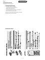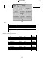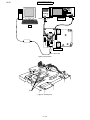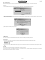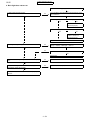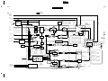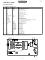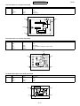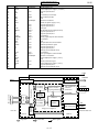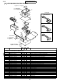
1
CONFIDENTIAL
GX15
SERVICE MANUAL
No. S5408TQGX5E//
DIGITAL MOBILE PHONE
MODEL
GX15
(INTERNAL MODEL NAME:
TQ-GX5E/G/R/T/S/H/EP/PP/W/B/D/A/Z/Q/L/F/U/GP)
E : For U.K.
R : For Ireland
S : For Spain
EP: For U.K. (Prepaid)
W : For Sweden
D : For Greece
Z : For New Zealand
L : For Malta
U : For Belgium
G : For Germany
T : For Italy
H : For Netherlands
PP: For Portugal (Prepaid)
B : For Hungary
A : For Australia
Q : For Egypt
F : For France
GP: For Germany (Prepaid)
• In the interests of user-safety the set should be restored to its
original condition and only parts identical to those specified
should be used.
• Caution
Risk of explosion if battery is replaced by an incorrect type,
dispose of used batteries according to the instruction.
CONTENTS
SERVICING CONCERNS
CHAPTER 1. GENERAL DESCRIPTION
[1] Specifications ................................................ 1-1
[2] Names of parts .............................................. 1-2
[3] Operation manual.......................................... 1-3
CHAPTER 2. ADJUSTMENTS,
PERFORMANCE CHECK,
AND FIRMWARE UPGRADE
[1] SHARP Programme Support Tool (SPST)........ 2-1
[2] Test points ................................................... 2-42
[3] Troubleshooting........................................... 2-44
CHAPTER 3. DISASSEMBLY AND REASSEMBLY
[1] Servicing Concerns ....................................... 3-1
[2] Disassembly and reassembly........................ 3-3
CHAPTER 4. DIAGRAMS
[1] Block diagram ................................................ 4-1
CHAPTER 5. SCHEMATIC DIAGRAM AND
WIRING SIDE OF P.W.BOARD
[1] Notes on schematic diagram ......................... 5-1
[2] Types of transistor and LED .......................... 5-1
[3] Waveforms of circuit ...................................... 5-2
[4] Schematic diagram/Wiring side of
P.W.Board ...................................................... 5-4
CHAPTER 6. OTHERS
[1] Function table of IC........................................ 6-1
[2] Function table of Camera ............................ 6-21
[3] Function table of Display ............................. 6-22
Parts Guide
Parts marked with "
" are important for maintaining the safety of the set. Be sure to replace these parts with specified ones for
maintaining the safety and performance of the set.
SHARP CORPORATION
This document has been published to be used
for after sales service only.
The contents are subject to change without notice.
GX15
CONFIDENTIAL
GX15
Phone
Service
E
Market
ManualCONCERNS
SERVICING
1. When requested, back up user’s handset data using SPST (SHARP Programme Support Tool). Otherwise, before servicing, warn the user that
data in the memory may be lost during repairs.
2. Upgrade the firmware to the latest version using SPST before returning the handset to the customer.
3. After repairs, inspect the handset (phone) according to the following flowchart.
Repairs are completed.
(Fixed parts have been checked for proper operation.)
Check IMEI NO./Operator code (Destination)/
Firmware version by Identity function of SPST.
Inspect each device using performance check
adjustment function of SPST.
Carry out RF performance check with SPST.
All completed.
4. When storing or transporting a PWB, put it into a conductive bag or wrap it in aluminum foil. (C-MOS IC may be damaged by electrostatic
charges.)
5. Do not leave fingerprints, etc. on ornamental parts including a cabinet, especially clear windows for main and sub displays. Wear fingerstalls to
avoid this.
Also, ensure not to leave fingerprints on the surface of display panel.
6. To prevent oxidation which causes connection problems, do not touch any terminals on the electric board, microphone, vibrator, earpiece and
speaker.
When handling these parts, wear fingerstalls. Should you touch these parts, clean them with a soft dry cloth.
Always wear fingerstalls when handling a shield case on the electric board. Otherwise oxidation may occur causing handset performance deterioration.
7. The FPC is a precision device. Handle it carefully to prevent any damages.
8. Do not expose the moisture sensor to liquids.
If the sheet gets wet, red ink runs. In this case, replace the sheet with a new one.
Be careful about your perspiration.
9. Before you disassemble or reassemble handset, make sure to remove the Li-Ion battery.
10.Be sufficiently careful with static electricity of integrated circuits and other circuits. Wear static electricity prevention bands whilst servicing.
i
CONFIDENTIAL
GX15
PRECAUTIONS FOR USING LEAD-FREE SOLDER
1 Employing lead-free solder
Lead-free solder is used for this model.
This is indicated by the “LF” symbol printed on the PWB and in the service manual.
The suffix letter indicates the alloy type of the solder.
Example:
Indicates lead-free solder of tin, silver and copper.
2 Using lead-free solder
When repairing a PWB with the “LF” symbol, only lead-free solder should be used. (Using normal tin/lead alloy solder may
result in cold soldered joints and damage to printed patterns.)
As the melting point of lead-free solder is approximately 40ºC higher than tin/lead alloy solder, it is recommended that a
dedicated bit is used, and that the iron temperature is adjusted accordingly.
3 Soldering
As the melting point of lead-free solder (Sn-Ag-Cu) is higher and has poorer wettability (flow), to prevent damage to the land
of the PWB, extreme care should be taken not to leave the bit in contact with the PWB for an extended period of time.
Remove the bit as soon as a good flow is achieved.
The high content of tin in lead free solder will cause premature corrosion of the bit.
To reduce wear on the bit, reduce the temperature or turn off the iron when it is not required.
Leaving different types of solder on the bit will cause contamination of the different alloys, which will alter their
characteristics, making good soldering more difficult.
It will be necessary to clean and replace bits more often when using lead-free solder. To reduce bit wear, care should be
taken to clean the bit thoroughly after each use.
ii
GX15
CONFIDENTIAL
GX15
Phone
Service
E
Market
Manual 1. GENERAL DESCRIPTION
CHAPTER
FOR A COMPLETE DESCRIPTION OF THE OPERATION OF THIS UNIT, PLEASE
REFER TO THE OPERATION MANUAL.
[1] Specifications
General:
Dimensions
(folded, excluding the aerial)
(H x W x D):
Weight:
Battery operating
temperature:
Display:
Camera:
Tti - band (GSM 900 MHz/DCS 1800 MHz/
PCS 1900MHz)
GPRS-enabled
WAP, MMS, SMS
Sound:
External DC
supply voltage:
Battery:
Standby time:
Talk time:
Others:
105 x 45 x 17.8 mm
84 g
0°C - 40°C
Display dimensions: 160 x 120 pixels
LCD display: CGS 65,536 colours with backlight
LCD back light: LED back light white colour LEDs
CMOS 310K pixels built-in camera
Zoom: Wide and zoom mode
[4 x zoom supported (when image size is
160 x 120 pixels)]
Lens: F2.8, f = 3.55 mm
Specifications for this model are subject to change without prior
notice.
Bluetooth is a trademark of the Bluetooth SIG, Inc.
The Bluetooth word mark and logos are owned by the
Bluetooth SIG, Inc. and any use of such marks by Sharp is
under license. Other trademarks and trade names are
those of their respective owners.
R
Licensed by Inter Digital Technology Corporation under one
or more of the following United States Patents and/or their
domestic or foreign counterparts and other patents pending, including U.S. Patents: 4,675,863: 4,779,262:
4,785,450 & 4,811,420.
Licensed under U.S. Patent 4,558,302 and foreign counterparts.
T9 Text Input is licensed under one or more of the following:
U.S. Pat. Nos. 5,818,437, 5,953,541, 5,187,480, 5,945,928,
and 6,011,554; Australian Pat. No. 727539; Canadian Pat.
No. 1,331,057; United Kingdom Pat. No. 2238414B; Hong
Kong Standard Pat. No. HK0940329; Republic of Singapore
Pat. No. 51383; Euro. Pat. No. 0 842 463 (96927260.8) DE/
DK, FI, FR, IT, NL,PT,ES,SE,GB; Republic of Korea Pat.
Nos. KR201211B1 and KR226206B1; and additional
patents are pending worldwide.
5.2 V
3.7 V, 780 mAh, Li-Ion
Up to 230 hours
Up to 230 minutes
Side key
Infrared port 1.2 L/P (maximum distance 20 cm)
Connector for AC charger and data cable
Standard hands free connector (ø2.5)
Battery running time depends on the battery and SIM card as well as
the network conditions and usage.
Powered by JBlend TM Copyright 19972004 Aplix Corporation. All rights reserved.
JBlend and all JBlend-based trademarks
and logos are trademarks or registered
trademarks of Aplix Corporation in Japan
and other countries.
Powered by Mascot Capsule /Micro3D Edition TM
R
Mascot Capsule is a registered trademark of HI Corporation
C 2002-2004 HI Corporation. All Rights Reserved.
40-polyphonic ring melodies
CP8 PATENT
This product is licensed under the MPEG-4 Visual Patent
Portfolio License for the personal and non-commercial use of
a consumer to (i) encode video in compliance with the
MPEG-4 Video Standard (“MPEG-4 Video”) and/or (ii) decode
MPEG-4 Video that was encoded by a consumer engaged in
a personal and non-commercial activity and/or was obtained
from a licensed video provider. No license is granted or
implied for any other use. Additional information may be
obtained from MPEG LA. See http://www.mpegla.com.
This product is licensed under the MPEG-4 Systems Patent
Portfolio License for encoding in compliance with the MPEG4 Systems Standard, except that an additional license and
payment of royalties are necessary for encoding in
connection with (i) data stored or replicated in physical media
which is paid for on a title by title basis and/or (ii) data which
is paid for on a title by title basis and is transmitted to an end
user for permanent storage and/or use. Such additional
license may be obtained from MPEG LA, LLC. See http://
www.mpegla.com for additional details.
1–1
GX15
CONFIDENTIAL
[2] Names of parts
1
2
8
16
13
20
3
4
5
6
7
7. * /Shift Key:
8. Display
9. Right Soft Key:
10.End/Power Key:
22
23
18
14
15
1. Earpiece
2. Navigation Keys (Arrow Keys):
Moves cursor to select
menu items, etc.
Up/Down arrow keys: Displays Contacts List
entries in stand-by mode.
Left arrow key:
Displays list of Applications
in stand-by mode.
Right arrow key:
Displays list of Saved
Pictures in stand-by mode.
3. Centre Key:
Displays Main menu in
stand-by mode and
executes functions.
4. Left Soft Key:
Executes the function at the
bottom left of the screen.
5. Send Key:
Makes or accepts calls,
views the call in stand-by
mode.
6. Voice Mail Key:
21
17
9
10
11
12
19
Press and hold this key to
connect to the Voice mail
centre automatically.
(Depends on the SIM card.)
Switches character case
among four modes: Abc,
ABC, 123 and abc.
Executes the function at the
bottom right of the screen.
Used to access “Vodafone
live!” by opening the
browser in stand-by mode.
Ends a call, turns power on/
off.
11.Keypad
1–2
12.# Key:
Switches symbol screens.
Press and hold this key on
the text entry screen to shift
text input method between
multi-tap and T9 mode.
Press and hold this key
during stand-by to switch
Profiles settings between
Normal and Silent mode.
Press , then
during
stand-by to activate Voice
Recorder.
13.Side-Up/Side-Down Keys:
Moves cursor to select
menu items, adjusts
earpiece volume, etc.
14.External Connector:
Used to connect either the
charger or USB data cable.
15.Microphone
16.Infrared Port:
Sends and receives data via
infrared.
17.Camera Key:
Starts the digital camera in
stand-by mode.
Takes pictures or records
videos in viewfinder mode.
18.Handsfree Kit Connector
19.Built-in Aerial:
Warning: Do not cover the
top of the phone with your
hand when in use as this
may interfere with the
performance of the built-in
aerial.
20.RF Connector
21.Camera
22.Self-Portrait Mirror: For taking a self-portrait.
23.Battery Cover
GX15
CONFIDENTIAL
[3] Operation manual
(Page numbers refer to the user guide)
[Optional Accessories]
Li-ion Spare battery (XN-1BT30)
Cigarette lighter charger (XN-1CL30)
USB data cable (XN-1DC30)
AC charger (XN-1QC30, XN-1QC31, XN-1QC32)
Personal handsfree kit (XN-1ER20)
The above accessories may not be available in all regions.
For details, please contact your dealer.
[Quickstart Guide]
1–3
CONFIDENTIAL
1–4
GX15
GX15
CONFIDENTIAL
1–5
GX15
CONFIDENTIAL
GX15
Phone
Service
E
Market
Manual 2. ADJUSTMENTS, PERFORMANCE CHECK, AND FIRMWARE
CHAPTER
UPGRADE
SPST (SHARP Programme Support Tool) allows you to adjust settings, conduct performance checks, and upgrade the firmware.
[1] SHARP Programme Support Tool (SPST)
1. System requirements
•
IBM PC compatible personal computer (standard COM1 115,200 bps serial port and USB required)
Recommended OS: Windows 2000/XP
Operable OS: Windows 98/98SE/ME
Incompatible OS: Windows 95/NT
(English, German, Italian, Spanish, French and Chinese versions)
•
Data cable
<During RF adjustment>
•
GSM tester: CMU200
•
GPIB interface: National Instruments USB-GPIB cable (Model No.: NI GPIB-USB-B)
2. Introduction
2.1. Functions
SPST offers seven key functions:
1) Firmware download
2) User data transfer (processes all data at once but not individually.)
3) RF calibration check and test
4) Default setting
5) Identification
6) Performance check and adjustment
7) User password reset
2.2. Installation
1. Use Windows Explorer to execute the “setup.exe” file on the CD-ROM.
2. The SPST GX15 setup wizard appears. Follow the installation instructions.
3. After the installation is complete, shortcuts to SPST are created on the desktop and under the “Start” — “Programs” — “GX15” menu. Start SPST
from the shortcuts.
2–1
GX15
CONFIDENTIAL
2.3. Starting up
Connect GX15 to an operable serial port of the PC with the supplied data cable. Make sure that the battery is fully charged.
Start SPST from the desktop.
1. The Input password dialogue box appears. Enter the password, select “GX15” from Port list box (a connected port is automatically detected), and
click “OK”. If you do not know SPC, click “Cancel” to exit.
When using SPST for the first time, the driver installation
starts and the following dialogue box appears.
After the installation is complete, press "Retry".
Figure 1
2. To change the password, enter the current password in Figure 1, and then click “Change Password”.
Figure 2
3. To check the usage status of tools, click “Show Repair Log” in Figure 1.
4. Click “Downloader for Emergency”.
Figure 3
The above screen appears. Select a model to use and execute the Downloader. (Use this to initialise the flash, etc.)
2–2
GX15
CONFIDENTIAL
5. When the password is correct, a connection is established and the following screen appears.
Refer to the attachment 1
for the destination and
operator name.
Software version:
A02-007-0119-GX15
Figure 4
Buttons
Default Set
User Data Back-up
User Data Restore
Downloader
RF Calibration & Check
RF Test
User Password Reset
Performance check adjustment
**** mode release
Exit
Refer to “4.1. Default setting”. (see page 2-5)
Refer to “4.2. User data back-up”. (see page 2-6)
Refer to “4.3. User data restore”. (see page 2-7)
Refer to “4.4. Downloader”. (see page 2-8)
Refer to “4.5. RF calibration & check”. (see page 2-19)
Refer to “4.6. RF test tool”. (see page 2-27)
Refer to “4.7. Password reset”. (see page 2-33)
Refer to “4.8. Performance check and adjustment”. (see page 2-34)
Refer to “4.9. ****mode release”. (see page 2-41)
End SPST.
Attachment 1 Destination and operator name list
No.
01
02
03
04
05
06
08
10
11
12
13
14
15
16
17
45
48
50
Operator name
Vodafone UK
Airtel
SFR
Vodafone Omnitel
D2
Vodafone NL
Vodafone Ireland
Vodafone Greece
Vodafone Hungary
Vodafone Australia
Vodafone New Zealand
Vodafone Sweden
Vodafone Egypt
Vodafone Malta
Swisscom
D2
Vodafone PT
Vodafone UK
Post-Paid
Post-Paid
Post-Paid
Post-Paid
Post-Paid
Post-Paid
Post-Paid
Post-Paid
Post-Paid
Post-Paid
Post-Paid
Post-Paid
Post-Paid
Post-Paid
Post-Paid
Pre-Paid
Pre-Paid
Pre-Paid
2–3
Country
UK
Spain
France
Italy
Germany
Netherlands (Holland)
Ireland
Greece
Hungary
Australia
New Zealand
Sweden
Egypt
Malta
Switzerland
Germany
Portugal
UK
Model name
A4TQGX15E
A4TQGX15S
A4TQGX15F
A4TQGX15T
A4TQGX15G
A4TQGX15H
A4TQGX15R
A4TQGX15D
A4TQGX15B
A4TQGX15A
A4TQGX15Z
A4TQGX15W
A4TQGX15Q
A4TQGX15L
A4TQGX15C
A4TQGX15GP
A4TQGX15PP
A4TQGX15EP
GX15
CONFIDENTIAL
3. Adjustments for GX15
1. Adjustments are required after replacing the following parts. (
Parts
Temperature
adjustment
(Camera)
)
Temperature
adjustment
(Battery)
Display flicker
adjustment
White defect
correction
Black defect
correction
TH102
Display unit
Camera unit
When replacing other parts in the RF section, carry out RF calibration.
2. Click the buttons on the SPST screen for adjustments.
RF calibration
To adjust the device, click this button
(Performance check adjustment).
Figure 5
3. The following screen appears.
Temperature adjustment (Camera section)
Temperature adjustment (Battery section)
Display flicker adjustment
White defect correction
Black defect correction
Figure 6
2–4
CONFIDENTIAL
4. Functions
4.1. Default setting
SPST can restore the factory settings.
This function
1. Deletes all user data in the file system;
2. Restores all WAP settings to default; and
3. Restores the values set by the user to default.
(MEPLOCK settings, the destination and operator name do not change.)
<Operation>
1) Set the COM port on the SPST initial screen and click “Default Set”.
2) Click “Yes” to proceed. Click “No” to exit.
Figure 7
3) Click “No” to back-up the MEPLOCK data. Click “Yes” to restore default settings.
Figure 8
4) Communication starts.
Figure 9
5) The following appears when you select “Yes” in step 3 and MEPLOCK data exists. Click “Yes” to restore the data.
Figure 10
2–5
GX15
GX15
CONFIDENTIAL
6) After the handset (phone) is turned on, the initialisation is complete.
Figure 11
4.2. User data back-up
SPST saves all the data stored on the handset (phone).
1. Set the COM port on the SPST initial screen and click “User Data Backup”.
2. Specify the file name in the following dialogue box and click “Save”.
Figure 12
3. The communicating dialogue box appears whilst processing.
Figure 13
4. When completed, the following message appears. Click “OK”.
Figure 14
2–6
CONFIDENTIAL
4.3. User data restore
SPST completely restores the backed up data.
1. Set the COM port on the SPST initial screen and click “User Data Restore”.
2. Specify the file name in the following dialogue box and click “Save”.
Figure 15
3. The communicating dialogue box appears whilst processing.
Figure 16
4. When the restore is complete, click “OK”.
Figure 17
2–7
GX15
GX15
CONFIDENTIAL
4.4. Downloader
4.4.1 Introduction
Downloader allows you to upgrade the firmware.
1) Required devices
•
PC (Operating System: Windows 2000, XP)
•
GX15 handset (phone)
•
USB hub
You can use a USB hub to download data to multiple handsets (phones) at a time.
(Recommended product) USB hub from Adaptec: XHUB7PLUS
Figure 18
Figure 19
•
USB download cable
GX15 USB download AC charger cable
USB data cable
Figure 20
*
The USB download cable consists of the GX15 USB download AC charger cable and a USB data cable.
*
A USB data cable is not the existing download cable.
*
The USB download cable is exclusively for download, not for any other purpose.
2–8
GX15
CONFIDENTIAL
2) Precautions
You can prevent problems from using the GX15 upgrading tool.
Please read the following before use.
*
Download may fail depending on the version of Windows.
It is recommended to update Windows to the latest version before you start.
*
Handsets (Phones) may not be recognised depending on the PC.
Disconnect the USB download cable connected with PC from the handset (phone) and reconnect.
If the handset (phone) is still not recognised, repeat a few times.
*
Make sure to remove the handset (phone) battery.
(Download must be performed without a battery inserted.)
*
Do not start/restart a PC with a handset (phone) connected.
*
If a PC is set to the power saving mode, disable it before download.
*
Whilst using a USB hub for download, do not use the remaining ports for other devices. Download may fail.
4.4.2 Installation of the device driver
Install the device driver (SHARP The Upgrading Tool USB Device Ver 0.90.0) on your PC.
1. Connect a PC and GX15 handset (phone) with the USB download cable.
[Make sure to remove the handset (phone) battery before connecting them.]
Figure 21
2. Install the device driver following the Hardware Wizard.
(For Windows 2000, the driver is automatically installed.)
Press "Next >" button.
Figure 22
2–9
GX15
CONFIDENTIAL
Press "Continue Anyway" button.
Figure 23
Screen during installation.
Figure 24
Press "Finish" button.
Figure 25 Screen after installation
*
Install the device driver for all handsets (phones) connected to the PC (including those via a USB hub).
*
If a handset (phone) is not recognised when connected to a PC:
Disconnect and reconnect the USB download cable.
[If the handset (phone) is still not recognised, repeat a few times.]
2 – 10
CONFIDENTIAL
GX15
4.4.3 Download
1) Application startup and screen descriptions
The icon below is created on your desktop after installation. Double-click it to start the Upgrading tool. You can also start the application by selecting
“The GX15 UpgradingTool” from the Start menu.
Figure 26
The download setup screen appears after starting the application.
1
2
3
4
Figure 27
1. Select Device: Shows port numbers of handsets (phones) recognised by the PC.
2. Select Load File: Specify a file to download.
3. Select Load Area: Select data space to store files.
4. Start Loading Flash: Press to start download.
2 – 11
GX15
CONFIDENTIAL
2) Download
<<Make sure the following before starting download>>
•
The handset (phone) battery is removed.
•
The device driver is installed on your PC.
•
Handset (Phone) is connected to a PC with the USB download cable.
<< Easy steps for download>>
1. Selecting a handset (phone)
When handset (phone) is recognised as a device, the corresponding Port No. box is checked.
[If the box is unchecked, data will not be downloaded to handset (phone).]
2. Selecting a download file
Select a file to download.
3. Selecting download area
<Example>
Check “Program Download” and “File System Initialize” and start download.
4. Starting download
Press “Start Loading Flash” button to start download.
5. Completing download
When download is successfully completed, “O” appears in the corresponding Port No. boxes. Click “OK” to exit.
Figure 28
2). 1 Selecting device
Check the corresponding Port No. box for the handset (phone) you want to download data to.
[When the handset (phone) is connected to a PC, the corresponding box is checked.]
Make sure the handset (phone) (without a battery) is connected to a PC with the USB download cable.
If the corresponding box cannot be checked, the handset (phone) may not be recognised correctly. Disconnect and reconnect the USB download
cable.
2 – 12
CONFIDENTIAL
GX15
2). 2 Selecting download file.
Select a file to download.
Press “Select File” button in “2. Select Load File”. The file selection screen appears.
Select a file to download and press “Open” button.
When you select a file, the file name appears in the text box. Proceed to “3. Select Load Area” becomes setting.
•
Only Motorola format (.mot) file can be downloaded.
•
You can select a file by entering a file name in the text box (without pressing “Select File” button). In this case, enter the file location together.
Figure 29 File selection screen
2). 3 Selecting download area
Usually select both “Program Download” and “File System Initialize”.
Figure 30
<“Program Download” and “File System Initialize”>
When both are selected, programme data is downloaded and user data area is initialised. Note that all the user data will be deleted after initialisation.
2 – 13
GX15
CONFIDENTIAL
2). 4 Starting download
Remove the handset (phone) battery before starting download.
•
“Start Loading Flash” button is disabled when handset (phone) is not connected to a PC.
Connect the PC and handset (phone) with the USB download cable.
•
If “Start Loading Flash” button is disabled after connecting the handset (phone):
Case 1: Handset (Phone) is not recognised by the PC.
Reconnect the PC and handset (phone) with the USB download cable.
Case 2: Some items are not selected on the download setup screen.
Make sure items of 1 - 3 are checked.
No handsets (phones) are connected.
A handset (phone) is connected.
Figure 31
Press “Start Loading Flash” button to start download.
Figure 32
2 – 14
GX15
CONFIDENTIAL
Download progress is shown on the PC and handset (phone).
Flash Loader V4.50
Port No.01
Now loading
Display on handset (phone)
(Port No. 1)
Display on PC
Figure 33 Screen during download
<< Aborting download>>
Press “Quit” button on the PC screen to stop download.
“Please wait for finishing process...” is displayed during the process. Do not disconnect the USB download cable until the message disappears.
Figure 34
2 – 15
GX15
CONFIDENTIAL
2). 5 Completing download
Press “OK” button before disconnecting the handset (phone).
When download is successfully completed, “O” appears as shown below.
In the screen shot, downloaded data are written to the handset (phone) correctly.
Flash Loader V4.50
Port No.01
Received SUM value
SUM = 0xbb7e
Display on handset (phone)
(Port No. 1)
Display on PC
Figure 35 Screen after download
<<Download errors>>
If download fails, “X” appears as shown below.
Disconnect and reconnect the USB download cable, and then retry.
Figure 36
2 – 16
GX15
CONFIDENTIAL
3) Download via a USB hub
Use a USB hub to download data to multiple handsets (phones) at a time.
[Up to 10 handsets (phones) at a time]
*
(Recommended product) USB hub from Adaptec: XHUB7PLUS (operation checked)
1. A USB hub is required. Use more according to the number of ports.
*When using more than one hub, connect them as shown in the section 3).1.
2. Connect the USB hub to a PC.
3. Into the USB hub, insert the same number of USB download cables as handsets (phones).
4. Connect the USB download cables to handsets (phones).
* Make sure handset (phone) batteries are removed.
5. Install the device driver (SHARP The Upgrading Tool USB Device Ver 0.90.0).
(For Windows 2000, the driver is automatically installed.)
6. On the download setup screen, port numbers become selectable for recognised handsets (phones).
Refer to the section “2) Download” to perform download.
Note:
Do not connect other devices to the remaining ports during download via a USB hub. Download may fail.
3). 1 Using multiple USB hubs
Connect multiple USB hubs according to the following.
1. Connection in series (recommended)
PC
USB
Hub
USB
Hub
Figure 37
2. Connection in parallel
PC
USB
Hub
USB
Hub
Figure 38
* When using more than one USB hubs, refer to the manuals to interconnect them.
4) Estimated download time
Download takes approximately 10 to 22 minutes when “Program Download” and “File System Initialize” are selected.
[Time depends on the number of handsets (phones) you are downloading data to.]
* Use of a USB 2.0 port will shorten the download time.
2 – 17
GX15
CONFIDENTIAL
4.4.4 Troubleshooting
This section describes error messages, solutions, and other important information.
* Error messages appear on the PC screen.
1) Error message list
No.
Displayed message
1
Unable to open file
2
Unable to Setup Device
3
The file you selected is unsuitable for Upgrading.
4
Download Error !!
Cause/Solution
Failed to open the MOT file to download.
The following are possible causes:
- The file path contains special characters.
Special characters: ~ ¥/:,;*?”<>|~
- The extension of the file is not “.mot”.
- The file is in use.
- The file path contains more than 257 bytes of characters.
- There is no drive letter in the file path.
- The file path is entered, but the file name is not.
- The file cannot be found.
- The file is located on a CD-ROM, removal disk, RAM disk or
network drive.
Check that the USB download cable is correctly connected to PC
and handset (phone).
The file is not downloadable.
Select a GX15 MOT file.
- Close running resident programmes.
- Close all other running applications.
- Reconnect the USB download cable and retry.
- Install Windows updates (see “4.4.1.2) Precoutions”)
* If an error occurs, disconnect and reconnect the USB download cable before you download again.
2) Other important information
•
Do not start /restart a PC with a handset (phone) connected.
(PC may freeze depending on the type.)
•
If the power saving mode is set on the PC, disable it before download.
(Download fails if the power saving mode is activated during the process and the PC may freeze.)
2 – 18
GX15
CONFIDENTIAL
4.5. RF calibration & check
RF cable
Stabilised power supply
Handset
(phone)
GSM tester
Test battery
GPIB cable
Data cable
PC
Figure 39
4.5.1 Preparation
•
Connect PC and GSM tester with a GPIB cable.
•
Connect PC and handset (phone) with a data cable. (Use a test battery or similar.)
•
Connect an RF cable of GSM tester to handset (phone).
2 – 19
GX15
CONFIDENTIAL
4.5.2 Default setting for the programme.
•
Activate the programme and set defaults.
1) A connected COM port
appears.
2) Set the GPIB No.
3) Select the test instrument.
4) Set the GPIB address.
5) Set the "Cable Offset" values.
For cables with connector
QCNWK0138AFZZ/
QCNWK0136AFZZ, set the
values as follows:
GSM 900: 0.60
DCS 1800: 0.95
PCS 1900: 0.96
6) Auto Dial Setting
When the Auto Dial check
box is checked, an entered
number is automatically
dialled for performance
check.
7) Number Setting
Enter a number for Auto Dial.
Figure 40
4.5.3 RF calibration
1. Apply 4 V using a stabilised power supply and turn on the handset (phone).
2. Start “RF calibration & check” on SPST and click “Cal”.
3. When initialisation is complete, the following message appears. Lower the stabilised power supply voltage to 3.7 V and click “OK”.
Figure 41
2 – 20
CONFIDENTIAL
4. Make sure the voltage is set properly and press “OK”.
(Calibration starts.)
Figure 42
5. Click “OK”.
Figure 43
6. The initial screen returns.
4.5.4 RF performance check
1. Apply 4 V using a stabilised power supply and turn on the handset (phone).
2. Start “RF calibration & check” on SPST and click “Check”.
3. When initialisation is complete, the following message appears. Lower the stabilised power supply voltage to 3.7 V and click “OK”.
Figure 44
4. Make sure the voltage is set properly and press “OK”.
(RF performance check starts.)
Figure 45
5. The following dialogue box appears after the check. Increase the stabilised power supply voltage to 4.0 V and click “OK”.
Figure 46
2 – 21
GX15
GX15
CONFIDENTIAL
6. Make sure the voltage is set properly and press “OK”.
Figure 47
7. RF performance check is complete. Click “Save As...” and name the file to save the result. Click “OK” to exit.
Figure 48
The following will be displayed in case of failure.
See the attachment 2 for troubleshooting.
Figure 49
2 – 22
CONFIDENTIAL
GX15
8. Click “OK”.
Figure 50
9. The initial screen returns.
Note:
The RF calibration tool allows the calibration but not the check when the terminal fails to catch signals from the GSM tester (unable to access a network with “no service” displayed). There is a possibility that CMU200 did not start properly. Turn off CMU200 and restart.
4.5.5 RF calibration & RF performance check
Pressing the “Cal_Check” button initiates RF calibration and RF performance check in succession.
Since some operations are skipped, this is handier than executing calibration (“Cal” button) and performance check (“Check” button) separately.
1. Set the stabilised power supply voltage to 4 V and turn on the handset (phone).
2. Start “RF calibration & check” on SPST and press “Cal_Check”.
3. Lower the stabilised power supply voltage to 3.7 V and press “OK”.
4. Make sure the voltage is set properly and press “OK”.
5. After the calibration and check, increase the stabilised power supply voltage to 4.0 V and press “OK”.
6. Make sure the voltage is set properly and press “OK”.
7. To save the results, press “Save As...” and enter a file name. To exit, press “OK”.
8. Press “OK”.
9. The initial screen returns.
(Steps 1 - 4 and 5 - 9 are respectively equivalent to RF calibration by the “Cal” button and RF performance check by the “Check” button.)
2 – 23
GX15
CONFIDENTIAL
Attachment 2
Whole inspection list by RF performance check.
Band
GSM
Sending/
Recei
ve
Tx
No.
1
2
3
4
5
6
7
8
9
10
11
12
13
14
15
16
17
18
19
20
21
22
23
24
25
26
27
28
29
30
31
32
33
34
35
36
37
38
39
40
41
42
43
44
45
46
47
48
49
50
51
52
53
54
55
56
57
58
59
60
Item to be inspected
Burst Power
Burst Power
Burst Power
Burst Power
Burst Power
Frequency Error
Frequency Error
Frequency Error
Phase Error (RMS)
Phase Error (RMS)
Phase Error (RMS)
Phase Error (Peak)
Phase Error (Peak)
Phase Error (Peak)
Mod_spectrum –800
Mod_spectrum –600
Mod_spectrum –400
Mod_spectrum –250
Mod_spectrum –200
Mod_spectrum +200
Mod_spectrum +250
Mod_spectrum +400
Mod_spectrum +600
Mod_spectrum +800
Mod_spectrum –800
Mod_spectrum –600
Mod_spectrum –400
Mod_spectrum –250
Mod_spectrum –200
Mod_spectrum +200
Mod_spectrum +250
Mod_spectrum +400
Mod_spectrum +600
Mod_spectrum +800
Mod_spectrum –800
Mod_spectrum –600
Mod_spectrum –400
Mod_spectrum –250
Mod_spectrum –200
Mod_spectrum +200
Mod_spectrum +250
Mod_spectrum +400
Mod_spectrum +600
Mod_spectrum +800
Mod_spectrum –800
Mod_spectrum –600
Mod_spectrum –400
Mod_spectrum –250
Mod_spectrum –200
Mod_spectrum +200
Mod_spectrum +250
Mod_spectrum +400
Mod_spectrum +600
Mod_spectrum +800
Mod_spectrum –800
Mod_spectrum –600
Mod_spectrum –400
Mod_spectrum –250
Mod_spectrum –200
Mod_spectrum +200
Band
Channel
PCL
37CH
975CH
124CH
37CH
37CH
37CH
975CH
124CH
37CH
975CH
124CH
37CH
975CH
124CH
37CH
37CH
37CH
37CH
37CH
37CH
37CH
37CH
37CH
37CH
975CH
975CH
975CH
975CH
975CH
975CH
975CH
975CH
975CH
975CH
124CH
124CH
124CH
124CH
124CH
124CH
124CH
124CH
124CH
124CH
37CH
37CH
37CH
37CH
37CH
37CH
37CH
37CH
37CH
37CH
37CH
37CH
37CH
37CH
37CH
37CH
PCL5
PCL5
PCL5
PCL11
PCL19
PCL5
PCL5
PCL5
PCL5
PCL5
PCL5
PCL5
PCL5
PCL5
PCL5
PCL5
PCL5
PCL5
PCL5
PCL5
PCL5
PCL5
PCL5
PCL5
PCL5
PCL5
PCL5
PCL5
PCL5
PCL5
PCL5
PCL5
PCL5
PCL5
PCL5
PCL5
PCL5
PCL5
PCL5
PCL5
PCL5
PCL5
PCL5
PCL5
PCL11
PCL11
PCL11
PCL11
PCL11
PCL11
PCL11
PCL11
PCL11
PCL11
PCL19
PCL19
PCL19
PCL19
PCL19
PCL19
Sending/
Recei
ve
Rx
DCS
2 – 24
Tx
No.
Item to be inspected
Channel
PCL
61
62
63
64
65
66
67
68
69
70
71
72
73
74
75
76
77
78
79
80
81
82
83
84
85
86
87
88
89
90
91
92
93
94
95
96
97
98
99
100
101
102
103
104
105
106
107
108
109
110
111
112
113
114
115
116
117
118
119
120
121
122
Mod_spectrum +250
Mod_spectrum +400
Mod_spectrum +600
Mod_spectrum +800
Switch_Spectrum –1800
Switch_Spectrum –1200
Switch_Spectrum –600
Switch_Spectrum –400
Switch_Spectrum +400
Switch_Spectrum +600
Switch_Spectrum +1200
Switch_Spectrum +1800
Switch_Spectrum –1800
Switch_Spectrum –1200
Switch_Spectrum –600
Switch_Spectrum –400
Switch_Spectrum +400
Switch_Spectrum +600
Switch_Spectrum +1200
Switch_Spectrum +1800
Switch_Spectrum –1800
Switch_Spectrum –1200
Switch_Spectrum –600
Switch_Spectrum –400
Switch_Spectrum +400
Switch_Spectrum +600
Switch_Spectrum +1200
Switch_Spectrum +1800
Switch_Spectrum –1800
Switch_Spectrum –1200
Switch_Spectrum –600
Switch_Spectrum –400
Switch_Spectrum +400
Switch_Spectrum +600
Switch_Spectrum +1200
Switch_Spectrum +1800
Switch_Spectrum –1800
Switch_Spectrum –1200
Switch_Spectrum –600
Switch_Spectrum –400
Switch_Spectrum +400
Switch_Spectrum +600
Switch_Spectrum +1200
Switch_Spectrum +1800
Burst Timing
Burst Timing
Burst Timing
Burst Timing
Burst Timing
Rx Sensitivity
Rx Sensitivity
Rx Sensitivity
Usable Receiver Level
Rx Level Reports
Burst Power
Burst Power
Burst Power
Burst Power
Burst Power
Frequency Error
Frequency Error
Frequency Error
37CH
37CH
37CH
37CH
37CH
37CH
37CH
37CH
37CH
37CH
37CH
37CH
975CH
975CH
975CH
975CH
975CH
975CH
975CH
975CH
124CH
124CH
124CH
124CH
124CH
124CH
124CH
124CH
37CH
37CH
37CH
37CH
37CH
37CH
37CH
37CH
37CH
37CH
37CH
37CH
37CH
37CH
37CH
37CH
37CH
975CH
124CH
37CH
37CH
37CH
975CH
124CH
37CH
37CH
699CH
512CH
885CH
699CH
699CH
699CH
512CH
885CH
PCL19
PCL19
PCL19
PCL19
PCL5
PCL5
PCL5
PCL5
PCL5
PCL5
PCL5
PCL5
PCL5
PCL5
PCL5
PCL5
PCL5
PCL5
PCL5
PCL5
PCL5
PCL5
PCL5
PCL5
PCL5
PCL5
PCL5
PCL5
PCL11
PCL11
PCL11
PCL11
PCL11
PCL11
PCL11
PCL11
PCL19
PCL19
PCL19
PCL19
PCL19
PCL19
PCL19
PCL19
PCL5
PCL5
PCL5
PCL11
PCL19
PCL5
PCL5
PCL5
PCL5
PCL5
PCL0
PCL0
PCL0
PCL5
PCL15
PCL0
PCL0
PCL0
GX15
CONFIDENTIAL
Band
Sending/
Recei
ve
No.
Item to be inspected
Channel
PCL
123
124
125
126
127
128
129
130
131
132
133
134
135
136
137
138
139
140
141
142
143
144
145
146
147
148
149
150
151
152
153
154
155
156
157
158
159
160
161
162
163
164
165
166
167
168
169
170
171
172
173
174
175
176
177
178
179
180
181
182
183
184
Phase Error (RMS)
Phase Error (RMS)
Phase Error (RMS)
Phase Error (Peak)
Phase Error (Peak)
Phase Error (Peak)
Mod_spectrum –800
Mod_spectrum –600
Mod_spectrum –400
Mod_spectrum –250
Mod_spectrum –200
Mod_spectrum +200
Mod_spectrum +250
Mod_spectrum +400
Mod_spectrum +600
Mod_spectrum +800
Mod_spectrum –800
Mod_spectrum –600
Mod_spectrum –400
Mod_spectrum –250
Mod_spectrum –200
Mod_spectrum +200
Mod_spectrum +250
Mod_spectrum +400
Mod_spectrum +600
Mod_spectrum +800
Mod_spectrum –800
Mod_spectrum –600
Mod_spectrum –400
Mod_spectrum –250
Mod_spectrum –200
Mod_spectrum +200
Mod_spectrum +250
Mod_spectrum +400
Mod_spectrum +600
Mod_spectrum +800
Mod_spectrum –800
Mod_spectrum –600
Mod_spectrum –400
Mod_spectrum –250
Mod_spectrum –200
Mod_spectrum +200
Mod_spectrum +250
Mod_spectrum +400
Mod_spectrum +600
Mod_spectrum +800
Mod_spectrum –800
Mod_spectrum –600
Mod_spectrum –400
Mod_spectrum –250
Mod_spectrum –200
Mod_spectrum +200
Mod_spectrum +250
Mod_spectrum +400
Mod_spectrum +600
Mod_spectrum +800
Switch_Spectrum –1800
Switch_Spectrum –1200
Switch_Spectrum –600
Switch_Spectrum –400
Switch_Spectrum +400
Switch_Spectrum +600
699CH
512CH
885CH
699CH
512CH
885CH
699CH
699CH
699CH
699CH
699CH
699CH
699CH
699CH
699CH
699CH
512CH
512CH
512CH
512CH
512CH
512CH
512CH
512CH
512CH
512CH
885CH
885CH
885CH
885CH
885CH
885CH
885CH
885CH
885CH
885CH
699CH
699CH
699CH
699CH
699CH
699CH
699CH
699CH
699CH
699CH
699CH
699CH
699CH
699CH
699CH
699CH
699CH
699CH
699CH
699CH
699CH
699CH
699CH
699CH
699CH
699CH
PCL0
PCL0
PCL0
PCL0
PCL0
PCL0
PCL0
PCL0
PCL0
PCL0
PCL0
PCL0
PCL0
PCL0
PCL0
PCL0
PCL0
PCL0
PCL0
PCL0
PCL0
PCL0
PCL0
PCL0
PCL0
PCL0
PCL0
PCL0
PCL0
PCL0
PCL0
PCL0
PCL0
PCL0
PCL0
PCL0
PCL5
PCL5
PCL5
PCL5
PCL5
PCL5
PCL5
PCL5
PCL5
PCL5
PCL15
PCL15
PCL15
PCL15
PCL15
PCL15
PCL15
PCL15
PCL15
PCL15
PCL0
PCL0
PCL0
PCL0
PCL0
PCL0
Band
Sending/
Recei
ve
Rx
PCS
2 – 25
Tx
No.
Item to be inspected
Channel
PCL
185
186
187
188
189
190
191
192
193
194
195
196
197
198
199
200
201
202
203
204
205
206
207
208
209
210
211
212
213
214
215
216
217
218
219
220
221
222
223
224
225
226
227
228
229
230
231
232
233
234
235
236
237
238
239
240
241
242
243
244
245
246
Switch_Spectrum +1200
Switch_Spectrum +1800
Switch_Spectrum –1800
Switch_Spectrum –1200
Switch_Spectrum –600
Switch_Spectrum –400
Switch_Spectrum +400
Switch_Spectrum +600
Switch_Spectrum +1200
Switch_Spectrum +1800
Switch_Spectrum –1800
Switch_Spectrum –1200
Switch_Spectrum –600
Switch_Spectrum –400
Switch_Spectrum +400
Switch_Spectrum +600
Switch_Spectrum +1200
Switch_Spectrum +1800
Switch_Spectrum –1800
Switch_Spectrum –1200
Switch_Spectrum –600
Switch_Spectrum –400
Switch_Spectrum +400
Switch_Spectrum +600
Switch_Spectrum +1200
Switch_Spectrum +1800
Switch_Spectrum –1800
Switch_Spectrum –1200
Switch_Spectrum –600
Switch_Spectrum –400
Switch_Spectrum +400
Switch_Spectrum +600
Switch_Spectrum +1200
Switch_Spectrum +1800
Burst Timing
Burst Timing
Burst Timing
Burst Timing
Burst Timing
Rx Sensitivity
Rx Sensitivity
Rx Sensitivity
Usable Receiver Level
Rx Level Reports
Burst Power
Burst Power
Burst Power
Burst Power
Burst Power
Frequency Error
Frequency Error
Frequency Error
Phase Error (RMS)
Phase Error (RMS)
Phase Error (RMS)
Phase Error (Peak)
Phase Error (Peak)
Phase Error (Peak)
Mod_spectrum –800
Mod_spectrum –600
Mod_spectrum –400
Mod_spectrum –250
699CH
699CH
512CH
512CH
512CH
512CH
512CH
512CH
512CH
512CH
885CH
885CH
885CH
885CH
885CH
885CH
885CH
885CH
699CH
699CH
699CH
699CH
699CH
699CH
699CH
699CH
699CH
699CH
699CH
699CH
699CH
699CH
699CH
699CH
699CH
512CH
885CH
699CH
699CH
699CH
512CH
885CH
699CH
699CH
661CH
512CH
810CH
661CH
661CH
661CH
512CH
810CH
661CH
512CH
810CH
661CH
512CH
810CH
661CH
661CH
661CH
661CH
PCL0
PCL0
PCL0
PCL0
PCL0
PCL0
PCL0
PCL0
PCL0
PCL0
PCL0
PCL0
PCL0
PCL0
PCL0
PCL0
PCL0
PCL0
PCL5
PCL5
PCL5
PCL5
PCL5
PCL5
PCL5
PCL5
PCL15
PCL15
PCL15
PCL15
PCL15
PCL15
PCL15
PCL15
PCL0
PCL0
PCL0
PCL5
PCL15
PCL0
PCL0
PCL0
PCL0
PCL0
PCL0
PCL0
PCL0
PCL5
PCL15
PCL0
PCL0
PCL0
PCL0
PCL0
PCL0
PCL0
PCL0
PCL0
PCL0
PCL0
PCL0
PCL0
GX15
Band
CONFIDENTIAL
Sending/
Recei
ve
No.
Item to be inspected
Channel
PCL
247
248
249
250
251
252
253
254
255
256
257
258
259
260
261
262
263
264
265
266
267
268
269
270
271
272
273
274
275
276
277
278
279
280
281
282
283
284
285
286
287
288
289
290
291
292
293
294
295
296
Mod_spectrum –200
Mod_spectrum +200
Mod_spectrum +250
Mod_spectrum +400
Mod_spectrum +600
Mod_spectrum +800
Mod_spectrum –800
Mod_spectrum –600
Mod_spectrum –400
Mod_spectrum –250
Mod_spectrum –200
Mod_spectrum +200
Mod_spectrum +250
Mod_spectrum +400
Mod_spectrum +600
Mod_spectrum +800
Mod_spectrum –800
Mod_spectrum –600
Mod_spectrum –400
Mod_spectrum –250
Mod_spectrum –200
Mod_spectrum +200
Mod_spectrum +250
Mod_spectrum +400
Mod_spectrum +600
Mod_spectrum +800
Mod_spectrum –800
Mod_spectrum –600
Mod_spectrum –400
Mod_spectrum –250
Mod_spectrum –200
Mod_spectrum +200
Mod_spectrum +250
Mod_spectrum +400
Mod_spectrum +600
Mod_spectrum +800
Mod_spectrum –800
Mod_spectrum –600
Mod_spectrum –400
Mod_spectrum –250
Mod_spectrum –200
Mod_spectrum +200
Mod_spectrum +250
Mod_spectrum +400
Mod_spectrum +600
Mod_spectrum +800
Switch_Spectrum –1800
Switch_Spectrum –1200
Switch_Spectrum –600
Switch_Spectrum –400
661CH
661CH
661CH
661CH
661CH
661CH
512CH
512CH
512CH
512CH
512CH
512CH
512CH
512CH
512CH
512CH
810CH
810CH
810CH
810CH
810CH
810CH
810CH
810CH
810CH
810CH
661CH
661CH
661CH
661CH
661CH
661CH
661CH
661CH
661CH
661CH
661CH
661CH
661CH
661CH
661CH
661CH
661CH
661CH
661CH
661CH
661CH
661CH
661CH
661CH
PCL0
PCL0
PCL0
PCL0
PCL0
PCL0
PCL0
PCL0
PCL0
PCL0
PCL0
PCL0
PCL0
PCL0
PCL0
PCL0
PCL0
PCL0
PCL0
PCL0
PCL0
PCL0
PCL0
PCL0
PCL0
PCL0
PCL5
PCL5
PCL5
PCL5
PCL5
PCL5
PCL5
PCL5
PCL5
PCL5
PCL15
PCL15
PCL15
PCL15
PCL15
PCL15
PCL15
PCL15
PCL15
PCL15
PCL0
PCL0
PCL0
PCL0
Tx
Rx
Test item
Burst Power
Frequency Error
Phase Error
Mod_spectrum
Switch_Spectrum
Burst Timing
Rx Sensitivity
Usable Receiver Level
Rx Level Reports
Band
Sending/
Recei
ve
Rx
No.
Item to be inspected
Channel
PCL
297
298
299
300
301
302
303
304
305
306
307
308
309
310
311
312
313
314
315
316
317
318
319
320
321
322
323
324
325
326
327
328
329
330
331
332
333
334
335
336
337
338
339
340
341
342
Switch_Spectrum +400
Switch_Spectrum +600
Switch_Spectrum +1200
Switch_Spectrum +1800
Switch_Spectrum –1800
Switch_Spectrum –1200
Switch_Spectrum –600
Switch_Spectrum –400
Switch_Spectrum +400
Switch_Spectrum +600
Switch_Spectrum +1200
Switch_Spectrum +1800
Switch_Spectrum –1800
Switch_Spectrum –1200
Switch_Spectrum –600
Switch_Spectrum –400
Switch_Spectrum +400
Switch_Spectrum +600
Switch_Spectrum +1200
Switch_Spectrum +1800
Switch_Spectrum –1800
Switch_Spectrum –1200
Switch_Spectrum –600
Switch_Spectrum –400
Switch_Spectrum +400
Switch_Spectrum +600
Switch_Spectrum +1200
Switch_Spectrum +1800
Switch_Spectrum –1800
Switch_Spectrum –1200
Switch_Spectrum –600
Switch_Spectrum –400
Switch_Spectrum +400
Switch_Spectrum +600
Switch_Spectrum +1200
Switch_Spectrum +1800
Burst Timing
Burst Timing
Burst Timing
Burst Timing
Burst Timing
Rx Sensitivity
Rx Sensitivity
Rx Sensitivity
Usable Receiver Level
Rx Level Reports
661CH
661CH
661CH
661CH
512CH
512CH
512CH
512CH
512CH
512CH
512CH
512CH
810CH
810CH
810CH
810CH
810CH
810CH
810CH
810CH
661CH
661CH
661CH
661CH
661CH
661CH
661CH
661CH
661CH
661CH
661CH
661CH
661CH
661CH
661CH
661CH
661CH
512CH
810CH
661CH
661CH
661CH
512CH
810CH
661CH
661CH
PCL0
PCL0
PCL0
PCL0
PCL0
PCL0
PCL0
PCL0
PCL0
PCL0
PCL0
PCL0
PCL0
PCL0
PCL0
PCL0
PCL0
PCL0
PCL0
PCL0
PCL5
PCL5
PCL5
PCL5
PCL5
PCL5
PCL5
PCL5
PCL15
PCL15
PCL15
PCL15
PCL15
PCL15
PCL15
PCL15
PCL0
PCL0
PCL0
PCL5
PCL15
PCL0
PCL0
PCL0
PCL0
PCL0
Troubleshooting list
Check parts for GSM
Check parts for DCS
IC802, FL803, FL905
IC802, FL803, FL905
–
–
–
–
–
–
IC802
IC802
IC802
IC802
FL803, FL902, FL905
FL803, FL902, FL905
–
–
FL803, FL902, FL905
FL803, FL902, FL905
2 – 26
Check parts for PCS
IC802, FL803, FL905
–
–
–
IC802
IC802
FL803, FL903, FL905
–
FL803, FL903, FL905
CONFIDENTIAL
4.6. RF test tool
4.6.1 Requirements
For repairs, this test checks the condition of an electric board (especially the RF section).
•
PC with USB port
•
GX15 data cable
•
PWB repair jig
•
GSM tester (CMU200)
4.6.2 Setup
1. Install GX15 USB driver from CD-ROM, if it is not installed.
2. Set PWB and make connections as shown in Figures 51 and 52.
Make sure connections are correct at the points shown in Figure 53.
Guide
PWB
Guide
Guide
Figure 51 PWB installation
2 – 27
GX15
GX15
CONFIDENTIAL
Black
Red
GSM tester
(CMU 200)
PC
PWB repair jig
Data cable
Figure 52 Connections
Points
Figure 53 Contact points
2 – 28
GX15
CONFIDENTIAL
3. Apply 4 V using a stabilised power supply and turn on the handset (phone).
Push
Figure 54 Turning power on
4. Start RF test tool.
5. Press the “Initialize & Read Data” button. (COM port is automatically selected.)
Figure 55
6. Change the voltage, if you need.
7. Click “OK” to proceed.
Figure 56
2 – 29
GX15
CONFIDENTIAL
4.6.3 Tests
1) BAND Select & Channel
Select a band and a channel to test. Settings are applied to all tests.
Input box
Band selection
Channel bar
Figure 57
[Procedure]
1. Select a band. (GSM, DCS or PCS)
2. Select or enter a channel using channel bar or input box.
2) TX test
Test burst transmission.
TX frequency of selected channels
Current PCL (Read only)
PCL bar
TX ON/OFF button
This indicator appears during
burst transmission.
Data patterns
Figure 58
[Procedure]
1. Select a band and channel. [see 4.6.3.1)]
2. Select PCL (Power Control Level) using PCL bar.
3. Select a data pattern.
4. Click TX ON to start burst transmission.
(You can check each part in this state.)
5. Click TX OFF to end burst transmission.
*
Data pattern (TSC 5) includes Training Sequence GSM 5, and other part is pseudo random data.
2 – 30
GX15
CONFIDENTIAL
GX15 TX power Table (25°C, voltage: 3.7[V])
PCL
5
6
7
8
9
10
11
12
13
14
15
16
17
18
19
GSM Band
GSM
[dBm]
33
31
29
27
25
23
21
19
17
15
13
11
9
7
5
DCS/PCS Band
PCL
DCS/PCS
[dBm]
0
30
1
28
2
26
3
24
4
22
5
20
6
18
7
16
8
14
9
12
10
10
11
8
12
6
13
4
14
2
15
0
Tolerance
+/–2 dB
+/–3 dB
+/–3 dB
+/–3 dB
+/–3 dB
+/–3 dB
+/–3 dB
+/–3 dB
+/–3 dB
+/–3 dB
+/–3 dB
+/–5 dB
+/–5 dB
+/–5 dB
+/–5 dB
Tolerance
+/–2 dB
+/–3 dB
+/–3 dB
+/–3 dB
+/–3 dB
+/–3 dB
+/–3 dB
+/–3 dB
+/–3 dB
+/–4 dB
+/–4 dB
+/–4 dB
+/–4 dB
+/–4 dB
+/–5 dB
+/–5 dB
3) RX test
The handset (phone) receives burst signals in this test.
RX frequency of selected channels
Current RX Gain (Read only)
RX Gain Setting bar
RX ON/OFF button
This indicator appears whilst
receiving burst signals.
Sniff ON/OFF
Figure 59
[Procedure]
1. Select a channel and band. [see 4.6.3.1)]
2. Select RX Gain using RX Gain Setting bar.
3. Choose Sniff ON or OFF.
4. Click “RX ON” to receive burst signals.
5. From GSM tester, send burst signals in the specified channel.
(You can check each part in this state.)
6. Click “RX OFF” to stop burst signals.
*
In this test, the reception timing cannot be synchronised with burst signals from Signal Generator or GSM tester.
*
The standard RX Gain Setting is:
(Input power at the aerial connector of the handset (phone)) + (RX Gain) = –16 dBm
Excessive input power or RX Gain may cause damage to the handset (phone).
2 – 31
GX15
CONFIDENTIAL
4) RSSI Measure
The handset (phone) notifies you of input power value at the aerial connector.
Measured Power box
Estimated Power
input box
(Integer only)
Measure button
Figure 60
[Procedure]
1. Connect the handset (phone) and GSM tester (or Signal Generator) with RF cable.
2. Select a band and channel. [see 4.6.3.1)]
3. Send signals (*) from GSM tester.
4. Enter the value of input power from GSM tester in integers (from –10 to –110) considering RF cable loss.
5. Press the “Measure” button.
6. The result appears in Measured Power box.
*
The signal type from GSM tester must be either of the following:
1. Continuous sine wave (without modulation) with the following frequency.
(Frequency of the measured channel) + 67.708 kHz
(e.g. channel: GSM 37ch → the result: 942.467708 MHz)
Power: –110 to –10 dBm
2. BCCH signal of the measured channel
Power: –110 to –10 dBm
Result
When the handset (phone) is properly calibrated, the error between “Estimated Power” and “Measured Power” is less than 3 dB.
4.6.4 Termination
Turn off the handset (phone) to ensure proper operations.
4.6.5 Trouble information
When switching DCS and PCS, change the channel number as well. Or the band does not change properly.
Example: If you change DCS 512 CH to PCS 512 CH, the band remains DCS.
2 – 32
CONFIDENTIAL
4.7. Password reset
SPST resets the password [handset (phone) code is set to “0000”].
<Operation>
1) Set the COM port on the SPST initial screen and click “User Password Reset”. Click “Yes” to reset. Click “No” to exit.
Figure 61
2) When completed, the following appears.
Figure 62
2 – 33
GX15
GX15
CONFIDENTIAL
4.8. Performance check and adjustment
With this function, SPST checks the performance of the handset (phone) and makes adjustments.
<Operation>
1) Set the COM port on the SPST initial screen and click “Performance check and adjustment”. The following dialogue box appears whilst processing.
Figure 63
2) When completed, the following is displayed. Click “Back to main menu” to exit.
Figure 64
The functions of each button are described below.
4.8.1 Back light check
The display back light turns on and the message appears on the PC.
Figure 65
Check the back light and press “OK”.
• If a failure occurs, see “9. Back Light does not turn on.” in [3] Troubleshooting.
2 – 34
CONFIDENTIAL
GX15
4.8.2 Key back light check
The keypad back light turns on and the message appears on the PC. Check the back light and press “OK”.
4.8.3 Battery voltage check
Click to display the current battery voltage.
• If a failure occurs, see “1. Power does not turn on.” in [3] Troubleshooting.
4.8.4 Vibrator test
Click to vibrate the handset (phone). Click “OK” to exit.
• If a failure occurs, see “5. Vibrator does not work.” in [3] Troubleshooting.
4.8.5 Melody test
A message describes test items. Click “Yes” to proceed and “No” to exit.
The order of the test items:
Earpiece → Hands free → Hands free (stereo) → Earpiece (analogue melody)
Troubleshooting (based on [3] Troubleshooting)
Trouble found by SPST
(1) Earpiece
(2) Hands free
(3) Hands free (stereo)
(4) Earpiece (analogue melody)
See "7. Earpiece (for loud speaker) does not work."
Sound is heard in audio test.
Parts between IC105 pin 10 and IC103 pin 93 are defective, or IC103 is defective.
No sound is heard in audio test.
See "Hands free kit (monaural headset)" in the section "3. No voice is heard from the earpiece."
Sound is heard in audio test.
Parts between IC105 pin 10 and IC103 pin 93; IC105 pin 11 and IC103 pin 94 are defective.
Otherwise IC103 is defective.
No sound is heard in audio test.
See "Hands free kit (stereo headset) - Option" in the section "3. No voice is heard from
the earpiece."
See "8. Video/Voice Recorder playback is impossible."
Otherwise parts between IC105 pin 10 and IC103 pin 93 are defective, or IC103 is defective.
2 – 35
GX15
CONFIDENTIAL
4.8.6 Audio test
The following appears.
Figure 66
Select a test item from Audio device. Check the output sound from the receiver by speaking to the microphone, etc. Click “Back to test menu” to return
to the previous screen.
Troubleshooting (based on [3] Troubleshooting)
Trouble found by SPST
(1)
Handset microphone
Handset receiver
(2)
Handset microphone
Hands free receiver
(1) & (2): No voice is heard.
(3)
Hands free microphone
Hands free receiver
(4)
Hands free microphone
Handset receiver
(1) & (2): No voice is heard.
See "Phone" in the section "2. Voice transmission/recording is impossible."
(1): Voice is heard.
(2): No voice is heard.
See "Hands free kit (monaural headset)" in the section "3. No voice is heard
from the earpiece" or "Hands free kit (stereo headset) - Option" in the section
"3. No voice is heard from the earpiece."
(1): No voice is heard.
(2): Voice is heard.
See "Phone" in the section "3. No voice is heard from the earpiece."
(3) & (4): No voice is heard.
See "Hands free kit (headset)" in the section
"2. Voice transmission/recording is impossible."
(3): Voice is heard.
(4): No voice is heard.
(3): No voice is heard.
(4): Voice is heard.
4.8.7 Camera check
The following appears.
Figure 67
Select a Camera mode from the list box. Click “Shutter” to check that the camera operates properly. Click “Back to performance check menu” to return
to the previous screen.
• If a failure occurs, see “12. Pictures cannot be taken.” in [3] Troubleshooting.
4.8.8 Memory check
Click “S-RAM” and “PSRAM” to see each test result.
For “Check Sum”, the calculation appears after the SPST communicating dialogue box.
2 – 36
CONFIDENTIAL
GX15
4.8.9 LCD test
Check that the specified colour appears on the main display.
• If a failure occurs, see “10. The display does not appear on Display.” in [3] Troubleshooting.
4.8.10 Temperature adjustment
The following appears.
Setting temp. indicates the current temperature. The relative temperature is displayed in the text box below.
(Only the relative temperature is adjustable.)
If displayed Setting temp. value differs from the current temperature, click “
“Save”.
” or “
” to set a correction value in the range of –99 to +99 and click
Correction value = (Setting temp.) --- (current temp.) + (displayed correction value)
Figure 68
4.8.11 Display flicker adjustment
The following is displayed.
Figure 69
Check a main display visually within a distance of 20 cm from a fluorescent light, and adjust the value to minimise flicker on the display with the “
and “
” buttons. Click “Save” and confirm that the main display does not flicker.
(Fine adjustment for DC voltage between display electrodes)
Enlarged view
(A black line appears
after each gradation line.)
8-level gradation pattern with alternate black and gradation lines (black and white)
Figure 70
2 – 37
”
GX15
CONFIDENTIAL
4.8.12 White defect correction
* White defect correction:
Defective pixels in a camera light sensor appear as bright points in the display even when light is blocked completely (display is all black). Perform
white defect correction to eliminate errors in these pixels.
1. Protect the handset (phone) camera from light completely with a black cover.
2. Click the “White defect correction” button. The following screen appears.
Figure 71
Click the “Yes” button and leave it for about 20 seconds. When completed, the following message appears.
Figure 72
When an error occurs, the corresponding message appears. Solve the problem according to “Solution”.
•
Error 1
Error message: “There are too many white cracks.”
Cause: The light is not sufficiently blocked.
Solution: Block the light completely and perform white defect correction again.
•
Error 2
Error message: “There are many white cracks.”
Cause: The light is not sufficiently blocked.
Solution: Block the light completely and perform white defect correction again.
•
Error 3
Error message: “There are too many white cracks cannot be rectified.”
Cause: There is a hardware error.
Solution: Replace the camera unit.
2 – 38
CONFIDENTIAL
GX15
4.8.13 Black defect correction
*Black defect correction:
Defective pixels in a camera light sensor appear as black points in the display even when a captured image is completely white (display is all white).
Perform black defect correction to eliminate errors in these pixels.
1) Requirements
•
Desk top type of fluorescent lamp
•
Black defect correction sheet
Figure 73
•
Illuminance meter
2) Procedure
1. Cover the camera section with the black defect correction sheet as shown in Figure 74.
Attach the sheet to the handset (phone)
firmly with clear scotch tape.
Figure 74
2. Check the distance from the fluorescent lamp by using an illuminance meter.
In the proper position for black defect correction, illuminance is between 8,000 and 10,000 lux.
Figure 75
2 – 39
GX15
CONFIDENTIAL
3. Hold the handset (phone) in the proper position.
Figure 76
4. Click the “Black defect correction” button.
The following message is displayed.
Figure 77
5. Click the “Yes” button. Communication starts.
Figure 78
6. The result is displayed within a minute as follows.
Figure 79
When an error occurs, the corresponding message appears. Solve the problem according to “Solution”.
•
Error 1
Error message: “There are too many black cracks.”
Cause: The light is too weak or strong.
Solution: At the proper distance from the light source (8,000 - 10,000 lux), perform black defect correction again.
•
Error 2
Error message: “There are many black cracks.”
Cause: The light is too weak or strong.
Solution: At the proper distance from the light source (8,000 - 10,000 lux), perform black defect correction again.
•
Error 3
Error message: “There are too many black cracks cannot be rectified.”
Cause: There is a hardware error.
Solution: Replace the camera unit.
2 – 40
CONFIDENTIAL
GX15
4.9. ****mode release
When the handset (phone) does not turn on and enter the normal mode, use this function to change ****mode to the normal mode.
<Operation>
1) Select the COM port on the SPST initial screen and click “****mode release”. The following dialogue box appears.
Figure 80
2) If SPST cannot communicate with the handset (phone), the following message is displayed. Make sure the handset (phone) is turned on and click
“Retry”. To exit, click “Cancel”.
Figure 81
3) When complete, the following message appears.
Figure 82
5. Other tests
SPST does not provide tests of Bluetooth/USB communication. Check them according to the following instructions.
5.1. Bluetooth
1) Connect GX15 to the network and check that a conversation (talking and listening) is possible using a Bluetooth headset.
Recommended Bluetooth headset:
JABRA BT200
PLANTRONICS M1000
PLANTRONICS M3000
2) Connect GX15 to another Bluetooth built-in handset (phone) or PC and check that text data can be transmitted and received properly via Bluetooth.
5.2. USB
Connect GX15 and a PC with a USB cable. Check that GX15 is recognised as a device.
If the USB driver for GX15 (SHARP GSM GPRS USB Driver) is not installed on the PC, “Found New Hardware” window appears and “Found New
Hardware Wizard” starts [the handset (phone) is recognised].
2 – 41
GX15
CONFIDENTIAL
[2] Test points
MAIN PWB-A (FRONT SIDE)
TP No.
TP801
TP802
TP103
TP139
TP137
TP106
TP153
TP135
TP116
TP114
TP122
TP133
TP117 TP148
TP193
TP147
TP115
TP138
TP134
TP143
TP197
TP199
TP801 TP802
TP140
TP196
TP141
TP155
TP182
TP154
TP130
TP157
TP131
TP136
TP156
TP127
TP128
TP126
TP104
TP105
TP107
TP108
TP109
TP118
TP125
TP149
TP150
TP151
TP152
TP179
TP180
TP181
TP162
Figure 83 TEST POINT
2 – 42
Signal name
VTCXO (2.9V)
VRF (2.9V)
GX15
CONFIDENTIAL
MAIN PWB-A (REAR SIDE)
TP No.
TP110
TP111
TP112
TP113
TP119
TP120
TP121
TP129
TP142
TP144
TP145
TP146
TP158
TP159
TP163
TP164
TP165
TP167
TP170
TP171
TP174
TP175
TP176
TP177
TP195
TP198
TP401
TP501
TP502
TP503
TP504
TP505
TP506
TP507
TP508
TP509
TP510
TP513
TP515
TP520
TP521
TP523
TP524
TP525
TP526
TP527
TP534
TP535
TP536
TP601
TP604
TP606
TP607
TP608
TP609
TP145
TP142
TP401
TP146
TP144
TP520
TP510
TP502
TP501
TP534
TP163
TP113
TP527
TP606
TP603
TP604
TP195
TP608
TP605
TP601
TP111
TP112
TP609
TP198
TP513
TP607
TP190
TP177
TP159
TP101
TP526
TP158
TP167
TP525
TP536
TP175
TP535
TP170
TP110
TP164
TP102
TP504
TP171
TP121
TP515
TP506
TP129
TP119
TP503
TP524
TP523
TP174
TP165
TP521
TP509
TP508
TP507
TP505
TP176
TP120
Figure 84 TEST POINT
2 – 43
Signal name
VEXT
VVIB
DGND
VVIB
MIC_INP
AIN2P_C
RECEIVER_OUT
USC [6]
SPEAKER/RECIVER1
SPEAKER/RECIVER2
SPEAKER/RECIVER1
SPEAKER/RECIVER2
MODE_SELECT
CHGIN_A (5.2V)
13MHZ_CLK
VABB
LIGHT1 (KEYLED2)
VRTC (1.8V)
VMEM (2.93V)
VCORE (1.8V)
LIGHT3 (KEYLED)
SIM_POWER
VMIC
AUXADC1
Terminal for MEMORY adhesion check 1
Terminal for MEMORY adhesion check 2
VSCR (3.0V)
DGND
VBAT
CHGIN
USC [1]
USC [2]
VBAT
VUSB (3.2V)
USC [5]
USC [4]
BATT
Flexible PWB insert check terminal 1
Flexible PWB insert check terminal 2
BATT
POWERONKEY
RXD
TXD
GENIE RX
GENIE TX
DGND
BATT_SENSE
Manufacture Specific
AUDIO_IN
VCAM (2.8V)
Terminal for CAMERA_IC adhesion check 1
Terminal for CAMERA_IC adhesion check 2
VCAM (1.8V)
DOUT6
DOUT0
GX15
CONFIDENTIAL
[3] Troubleshooting
1.
2.
3.
4.
5.
6.
7.
8.
9.
10.
11.
12.
13.
14.
15.
16.
Power dose not turn on.
Voice transmission/recording is impossible.
No voice is heard from the earpiece.
Battery does not charge.
Vibrator does not work.
Clock Settings are reset.
Earpiece (for loud speaker) does not work.
Video/Voice Recorder playback is impossible.
Back Light does not turn on.
Out of range and incoming/outgoing calls are impossible.
The display does not appear on Display.
Pictures cannot be taken.
SIM card is not recognised.
IrDA (Infrared) communication is impossible.
Bluetooth communication is impossible.
USB connection is impossible.
See page 2-44
See page 2-46
See page 2-48
See page 2-49
See page 2-49
See page 2-50
See page 2-50
See page 2-51
See page 2-52
See page 2-53
See page 2-54
See page 2-55
See page 2-56
See page 2-57
See page 2-58
See page 2-58
1. Power dose not turn on.
Connect a battery of 4.0 V or more.
Execute File System initialisation of Downloader in SPST
without loading a file.
Does File System initialisation start properly?
YES
NO
Is the user area (file system) initialised by Flash Loader?
NO
YES
Flash memory (IC104) and
IC106 are defective.
Does normal mode start?
YES
NO
Flash memory (IC104) data is
corrupted.
Is it possible to rewrite the firmware?
NO
YES
Flash memory (IC104) and
IC106 are defective.
Does normal mode start after restart?
NO
Flash memory (IC104) and
IC106 are defective.
A
(To page 2-45)
2 – 44
YES
Programme code of Flash
memory (IC104) is garbled.
CONFIDENTIAL
GX15
(From page 2-44)
A
Is 3.6 V or more applied to BATT terminal (TP520)?
NO
Battery terminals are defective, connector terminal is dirty, or
soldering is improper.
YES
Is the voltage 1.2 V or lower on SENSE terminal (TP534)?
NO
The battery is defective or set improperly.
YES
Is there conduction through fuse (FS501)?
NO
Fuse (FS501) is blown.
NO
Flash memory (IC104) is installed improperly.
NO
IC103 is defective.
NO
X101 (32 kHz oscillator), R167, R169, C174, and C176 are
defective or mounted improperly.
Or oscillating circuit of IC106 is defective.
YES
Is Flash memory (IC104) installed properly?
YES
Are voltages of 2.93, 2.93, and 1.82 V applied to VMEM
(TP170), VEXT (TP110), and VCORE (TP171) respectively?
YES
Is the waveform of signals from R169 connected to X101 (32
kHz) correct?
Are R167, R169, C174, C176, X101, and IC106 good in
appearance and mounted properly?
YES
Is the triangular wave of 13 MHz sent from C833?
YES
IC801 is defective.
NO
Voltage Regulator (IC804) is defective.
NO
Is 2.9 V supplied from VTCXO (TP801)?
YES
IC801 and peripheral circuits are defective.
2 – 45
GX15
CONFIDENTIAL
2. Voice transmission/recording is impossible.
Phone (Handset)
Replace the microphone.
Is the problem solved?
YES
NO
The built-in microphone is defective or in a poor contact with
the PWB.
L101, L102, and C101 are defective.
YES
Is 1.2 - 2.1 V applied to both ends of C101?
NO
Is 1.2 - 2.1 V applied to TP119?
NO
YES
Is 2.4 - 2.6 V applied to TP176?
YES
NO
R125 is defective.
Is 2.4 - 2.6 V applied to IC103 pin 76?
YES
NO
R115 and C108 are defective.
IC103 is defective.
Is approx. 1.7 V applied to IC103 pin 80?
NO
Is approx. 1.7 V applied to IC103 pin 96?
NO
YES
R263 and R118 are defective.
Is 0.5 V or more applied to R101 (IC103 pin 9 side)?
YES
IC103 is defective.
YES
IC103 is defective.
YES
Parts between socket JK101 pin 5 and IC103 pin 9 are defective.
YES
Socket JK101 is defective.
YES
Parts between socket JK101 pin 3 and TP120 are defective.
NO
Is 0.5 V or more applied to JK101 pin 5?
NO
Is 0.5 V or more applied to JK101 pin 3?
NO
Is 0.5 V or more applied to TP120?
NO
YES
Is 2.4 - 2.6 V applied to TP176?
R122 is defective.
NO
Is 2.4 - 2.6 V applied to R115 (IC103 pin 76 side)?
YES
R115 is defective. (Headset mode is set.)
NO
Replace C121A or C133. Is the problem solved?
YES
NO
IC103 and IC106 are defective.
2 – 46
C121A or C133 is defective.
GX15
CONFIDENTIAL
Hands free kit (Headset)
Replace the hands free kit.
Is the signal sent?
YES
NO
Hands free kit is defective.
Parts between JK101 pin 3 andTP120 are defective.
YES
Is 0.7 - 1.8 V applied to JK101 pin 3?
NO
Is 0.7 - 1.8 V applied to TP120?
NO
YES
Is 2.4 - 2.6 V applied to TP176?
YES
NO
R122 is defective.
Is 2.4 - 2.6 V applied to IC103 pin 76?
YES
NO
R115 and C108 are defective.
IC103 is defective.
Is approx. 1.7 V applied to IC103 pin 79?
NO
Is approx. 1.7 V applied to IC103 pin 95?
NO
YES
R262 and R117 are defective.
Disconnect the hands free kit. Is speaking voice heard to the
person in the phone mode?
YES
IC103 is defective.
NO
IC103 or IC106 is defective.
NO
Socket JK101 is defective. (Phone mode is set.)
YES
C123A is defective.
YES
JK101 is defective, or the socket plug pin 3 is in a poor contact
with hands free kit.
YES
Is the voltage 0 V on R101 (IC103 pin 9 side)?
YES
Replace C123A. Is the problem solved?
NO
Replace JK101. Is the problem solved?
NO
IC103 and IC106 are defective.
2 – 47
GX15
CONFIDENTIAL
3. No voice is heard from the earpiece.
Phone (Handset)
Do keypad tones and melodies sound?
NO
Go to the section “Earpiece (for loud speaker) does not work”.
(see page 2-50)
YES
Is 0.5 V or more applied to R101 (IC103 pin 9 side)?
YES
IC103 is defective.
NO
Is 0.5 V or more applied to JK101 pin 5?
YES
Parts between socket JK101 pin 5 and IC103 pin 9 are defective.
NO
Is 0.5 V or more applied to JK101 pin 3?
YES
Socket JK101 is defective.
NO
Is 0.5 V or more applied to TP120?
YES
Parts between socket JK101 pin 3 and TP120 are defective.
NO
YES
Is 2.4 - 2.6 V applied to TP176?
R122 is defective.
NO
Is 2.4 - 2.6 V applied to R115 (IC103 pin 76 side)?
YES
R115 is defective. (Hands free kit mode is set.)
NO
IC103 is defective.
Hands free kit (Headset)
Replace the hands free kit. Is sound produced?
YES
The hands free kit is defective.
YES
Socket JK101 is defective, or the hands free kit is in a poor
contact with the socket plug.
NO
Is signal sent to JK101 pin 4?
NO
YES
Is signal sent to TP121?
Parts between socket JK101 pin 4 and TP121 are defective.
NO
Is signal sent to R124 (IC103 pin 60 side)?
YES
Parts between IC103 pin 60 and TP120 are defective.
NO
IC103 or IC106 is defective.
YES
IC103 is defective.
NO
Disconnect the hands free kit. Is voice heard in phone mode?
YES
Is the voltage 0 V on R101 (IC103 pin 9 side)?
NO
Socket JK101 is defective.
2 – 48
CONFIDENTIAL
GX15
4. Battery does not charge.
Set a battery of 4.0 - 4.2 V. Click the “Performance check
adjustment” button on SPST.
YES
Click the “Temperature adjustment” button. Is the value of
“temp” normal? (Measurement tolerance: ± 5 deg.)
* For settings and connections for SPST, refer to the “ADJUSTMENTS,
PERFORMANCE CHECK, AND FIRMWARE UPGRADE” on page 2-1.
TH102 and IC103 are defective.
NO
YES
Click the “Battery voltage check” button. Is the voltage 4.0 4.2 V?
NO
IC103 is defective.
NO
R535, R536, Q102, and IC107 are defective.
NO
IC107 is defective.
NO
R535, R536, Q102, IC107, IC102, Q101, IC103, D101, and
D102 are defective.
NO
Vibrator is deformed and defective. (When vibrator terminals
and the land are dirty, clean or replace them.)
YES
Set a battery of 3.7 - 3.9 V and start in normal mode.
Connect the AC charger to the external connector.
Is the voltage applied to TP503 higher than that of battery?
YES
When the AC charger is inserted to the external connector, is
IC107 pin 1 at “L”?
YES
Connect the AC charger to the external connector.
After approx. 15 seconds, do the voltages on TP159 and
TP502, and TP506 increase by more than 0.05 V?
YES
The battery is defective, or the battery cycle is shortened.
5. Vibrator does not work.
Are vibrator terminals in contact with the land?
Are terminals and the land clean?
YES
Hereafter check with vibrator working.
Is rectangular wave of 3 V sent to between vibrator terminals
YES
in sync with the vibration pattern?
Vibrator is defective.
NO
Is VBAT voltage applied to IC108 pin 4?
NO
IC108 is soldered improperly.
YES
IC108 is defective.
YES
IC101 is soldered improperly.
NO
Go to the section “Earpiece (for loud speaker) does not work”.
(see page 2-50)
YES
Is signal synchronised with the vibration pattern sent to IC108
pin 3?
NO
Is signal synchronised with the vibration pattern sent from
IC101 pin 19?
NO
Do ring tones sound from earpiece (for loud speaker)?
YES
IC101 is defective.
2 – 49
GX15
CONFIDENTIAL
6. Clock Settings are reset.
Is 1.6 V or more applied to TP167 with a battery in the phone?
NO
YES
IC103 is defective.
The back-up battery holder is installed improperly.
NO
Is 1.2 V or more applied to TP167 without a battery in the
phone?
NO
Is back-up battery holder properly installed to Main PWB?
YES
YES
• The remaining power of back-up battery is insufficient.
• Back-up battery is defective.
• Back-up battery holder is defective.
• Main PWB is broken, or CN104 is defective.
• R254 is defective.
X101, R169, C174, and C176 are defective.
7. Earpiece (for loud speaker) does not work.
* When ring tones sound, but keypad tones do not, “Keypad Tones” is set to Off.
* When only ring tones do not sound, “Ringer Volume” is set to “Silent”.
* Ring tones sound according to “Ringer Volume” settings.
Are earpiece terminals in contact with the land?
NO
The earpiece is defective.
NO
The earpiece is defective.
YES
The earpiece is defective.
YES
Is the impedance between earpiece terminals approx. 8
ohms?
YES
Is signal sent to TP145, TP146, or the earpiece contact pad?
NO
Is signal sent to IC103 pins 91, 107, 89, and 105?
YES
NO
Either of following parts are defective:
· Between IC103 pins 91/107 and TP145
· Between IC103 pins 89/105 and TP146
IC109 is defective.
YES
Is 3 V supplied from IC109 pin 5?
NO
Is VBAT voltage applied to IC109 pin 1 and VCORE voltage
(1.8 V) to pin 3?
NO
YES
IC109 is soldered improperly.
YES
Is signal sent to IC103 pin 93?
IC103 is defective.
NO
Does a hands free kit produce ring tones?
YES
IC103 is defective.
YES
Parts between IC101 pin 10 and IC103 pin 93 are defective.
NO
Is signal sent to IC101 pin 10?
NO
Is approx. 3 V applied to IC101 pins 7 and 32?
NO
YES
IC101 or the control line to IC106 is defective.
2 – 50
Short-circuit between VEXT and IC101 pin 7 is soldered
improperly.
GX15
CONFIDENTIAL
8. Video/Voice Recorder playback is impossible.
Earpiece
Are keypad tones and ring tones normal?
NO
Go to the section “Earpiece (for loud speaker) does not work.”
(see page 2-50)
NO
IC104 or IC106 is defective.
YES
In Playback window, does playback start normally and the
capacity bar change?
YES
Not defective.
YES
Is Multimedia Volume set to “Silent”?
YES
Cancel “Silent”. Is sound produced?
NO
Is voice heard in phone mode?
NO
NO
Go to “Phone (Handset)” in the section “No voice is heard
from the earpiece.” (see page 2-48)
YES
Hands free kit is defective.
NO
IC104 or IC106 is defective.
YES
IC103 or IC106 is defective.
Hands free kit (Headset)
Replace the hands free kit.
Is the signal sent?
NO
In Playback window, does playback start normally and the
capacity bar change?
YES
Not defective.
YES
Is Multimedia Volume set to “Silent”?
YES
NO
Is voice heard in hands free kit mode?
Cancel “Silent”. Is sound produced?
NO
NO
YES
IC103 or IC106 is defective.
2 – 51
Go to “Hands free kit (Headset)” in the section “No voice is
heard from the earpiece.” (see page 2-48)
GX15
CONFIDENTIAL
9. Back Light does not turn on.
FS502 is mounted improperly, or the fuse is blown.
NO
Is VBAT voltage applied to C530?
NO
Is fuse (FS502) in good appearance, mounted properly, and is
there conduction?
YES
YES
Is IC506 in good appearance and mounted properly?
NO
YES
IC506 is defective or
mounted improperly.
Is 0.8 V or more applied to IC506 pin 4?
NO
YES
C506, R523, R549, and
IC106 are defective or
mounted improperly.
C530, L502, and IC506 are defective.
Is back light setting for Display set to On?
NO
Go to the setting as follows and set it to On:
Settings → Display → Back light → Time out
YES
NO
Does it turn on?
YES
Not defective.
Are R527 and R547 in good appearance and mounted properly?
NO
R527 and R547 are defective.
NO
IC506 is mounted improperly or defective.
YES
Is approx. 10.2 V applied between LED501 anode (A) terminal
and LED503 cathode (K) terminal?
YES
LED501, LED502, and LED503 are mounted improperly or
defective.
2 – 52
CONFIDENTIAL
10. Out of range and incoming/outgoing calls are impossible.
[Checkpoints in RF Test Tool]
Is transmission possible using RF Test Tool?
YES
[Sender]
NO
Is frequency signal sent to FL803?
EGSM900 band ...................... IC803 pin 15
DCS1800/PCS1900 bands ..... IC803 pin 13
NO
Main PWB-A is defective.
YES
Is frequency signal supplied to pin 1 of FL905?
NO
FL803 is defective.
NO
FL905 is defective.
YES
Is frequency signal supplied to pin 1 of J801?
YES
J801 is defective.
[Receiver]
Is frequency signal sent from FL902 or FL903?
EGSM900 band ........................... FL902 pins 6, 7
DCS1800 band ............................ FL902 pins 8, 9
PCS1900 band ............................ FL903 pins 3, 4
Main PWB-A is defective.
YES
NO
Is frequency signal supplied to FL902 or FL903?
EGSM900 band ........................... FL902 pin 4
DCS1800 band ............................ FL902 pin 1
PCS1900 band ............................ FL903 pin 1
FL902 or FL903 is defective.
YES
NO
Is frequency signal supplied to pin 9 of FL803?
YES
NO
FL905 or J801 is defective.
2 – 53
FL803 is defective.
GX15
GX15
CONFIDENTIAL
11. The display does not appear on Display.
Is Display unit fully inserted to CN102?
NO
Improperly inserted to the connector.
NO
The contact point of the connector is dirty.
YES
Display unit is defective.
NO
Go to the section “Power dose not turn on.” (see page 2-44)
YES
Clean the contact point of CN102 and insert the unit again.
Does the display appear?
YES
Replace Display.
Does the display appear?
NO
Is 3.6 or more voltage applied to VBAT terminal
(IC110 pin 4) ?
YES
Go to the section “Power dose not turn on.” (see page 2-44)
NO
Is 2.93 + 0.37, – 0.53 V applied to VDC terminal (CN102 pin
15 to VEXT)?
NO
Is short terminal (between CN102 pin 15 and VEXT) defective?
YES
YES
Short terminal is defective.
Regulator IC110 is mounted improperly or short terminal is
soldered improperly.
NO
Is 3.0 ± 0.1 V or more applied to VCC2 terminal (CN102 pin
14 to IC110 pin 3)?
NO
Are IC110 and short terminal (between IC110 pin 3 and
CN102 pin 14) good in appearance and mounted properly?
YES
YES
Regulator IC110 is defective.
Capacitors C215 (between C1+ and C1-) and C212/C194
(between C2+ and C2-) are defective or mounted improperly.
NO
Is voltage on VDD2 terminal (C194) boosted to approx. 6 V?
NO
Are capacitors C215 (between C1+ and C1-) and C212/C194
(between C2+ and C2-) in good appearance and mounted
properly?
YES
YES
Display unit is defective.
Is the voltage approx. -10 V on VSS2 terminal (C200) and
approx. 15 V on VDD1 terminal (C211)? Are capacitors C209,
C210, C217, C218, C200, and C211 in good appearance and
mounted properly?
NO
Capacitors C209, C210, C217, C218, C200, and C211 are
defective or mounted improperly.
YES
Is approx. 3 V applied to LCD reset (R178)? Is R178 in good
appearance and mounted properly?
NO
R178 is defective or mounted improperly. Otherwise the digital
IC (IC105) is defective.
YES
Are C216, C218, C221, C222, C223, C227, R157, R176,
R186, R197, R142, R151, R152, and R154 good in appearance and mounted properly?
NO
YES
Display unit is defective, or connector CN102 is mounted
improperly.
2 – 54
C216, C218, C221, C222, C223, C227, R157, R176, R186,
R197, R142, R151, R152, and R154 are defective or mounted
improperly.
GX15
CONFIDENTIAL
12. Pictures cannot be taken.
Is the camera (CA100) installed in the right direction?
NO
Reinsert the camera (CA100).
NO
IC603 is mounted improperly.
NO
SO601 is mounted improperly.
NO
The camera (CA100) is defective.
(Most likely poor contact caused by adhesive on pins)
YES
Check that IC603 has not come off.
Is there conduction between TP604 and TP606?
YES
Are all the pins of SO601 mounted properly?
YES
Replace the camera (CA100). Does the camera turn on?
YES
The regulator IC602 or peripheral circuits are defective.
NO
Is 2.8 V applied to SO601 pins 5, 10, and 23 (when camera is
on)?
NO
Is 2.8 V applied to TP601?
YES
YES
Short terminal (TP601 to SO601 pin 23) and (TP601 to
SO601 pin 5) are defective.
IC603/IC106 is defective, or R602/C607 is mounted improperly.
NO
SO601:
1. Is 2.8 V applied on pins 4 and 7?
2. Is the voltage 0 V on pin 8?
3. Is the 13 MHz frequency sent to pin 1?
(when camera is on)
NO
IC603 peripheral circuits:
1. Is 13 MHz frequency sent to R602?
2. Is 2.93 V applied to C607?
(when camera is on)
YES
YES
Is 1.8 V applied to IC603 peripheral circuit TP607 (when camera is on)?
NO
YES
IC601 or peripheral circuits
are defective; R605/C609 is
mounted improperly.
Is 2.93 V applied to IC603 peripheral circuit R604
(when camera is on)?
NO
YES
IC103 or peripheral circuits
are defective; R604/C608 is
mounted improperly.
IC603 or IC106 is defective.
R606 and C610 are mounted improperly.
R606 is defective.
NO
SO601:
1. Is 2.8 V applied on pins 2 and 3 (when camera is on)?
2. Are voltages of pins 2 and 3 within the range 0 to 2.8 V
(when camera being activated)?
NO
Is 2.8 V applied to IC603 peripheral circuit R606
(when camera is on)?
YES
YES
IC603 is defective.
B
(To page 2-56)
2 – 55
GX15
CONFIDENTIAL
(From page 2-55)
B
SO601:
Are voltages of the following pins within the range 0 to 2.8 V
(when camera is on)?
1. pins 11 - 18
2. pins 20 - 22
NO
R611, R612, and R613 are mounted improperly.
YES
IC603 is defective.
13. SIM card is not recognised.
Replace the SIM card. Is it recognised?
NO
Is 2.85 V supplied from pins 1, 2, and 6 of the SIM card?
And is periodic pulse wave (3.25 MHz) sent from pin 3 of the
SIM card?
YES
SIM card is defective or not the one specified.
Hereafter, check the signal waveform of each SIM when the power is turned on
without a SIM card inserted.
(SIM signal waveform appears for approx. 70 ms after the power is turned on.)
YES
NO
The contact point of the SIM card connector is deformed or
dirty.
R110 or C131 is defective.
NO
Is 2.85 V applied to CN101 pin 1?
NO
Are R110 and C131 good in appearance and mounted properly?
YES
YES
IC103 is defective.
Short terminal (CN101 pin 1 to IC106 pin 195) is defective.
NO
Is 2.85 V applied to CN101 pin 2?
NO
Is short terminal (CN101 pin 1 to IC106 pin 195) good in
appearance and mounted properly?
YES
YES
IC106 is defective.
R164 is defective.
NO
Is periodic pulse wave sent from CN101 pin 3?
NO
Is R164 good in appearance and mounted properly?
YES
YES
IC106 is defective.
Replace R163, R113, or short terminal (CN101 pin 6 to R163).
NO
Is 2.85 V supplied from CN101 pin 6?
NO
Are R163, R113, and short terminal (CN101 pin 6 to R163)
good in appearance and mounted properly?
YES
YES
CN101 is defective.
IC106 is defective.
2 – 56
GX15
CONFIDENTIAL
14. IrDA (Infrared) communication is impossible.
Set the distance and angle within the specification for the IrDA
communication.
Is 2.8 V supplied from Q104 pin 2?
Check in IrDA inspection mode.
NO
IC106 is defective.
YES
Is 2.8 V applied to UN101 pin 6?
NO
YES
Q104 is defective or UN101 pin 6 is soldered improperly.
R183 is defective.
NO
Does the send signal (UN101 pin 5) send pulse waves periodically?
NO
Is R183 good in appearance and mounted properly?
YES
YES
IC101 or IC106 is defective.
Short terminal (CN101 pin 2 to VEXT) and C197 are defective.
NO
Is 3.0 V supplied from VCC (UN101 pin 1)?
NO
Are short terminal (CN101 pin 2 to VEXT) and C197 good in
appearance and mounted properly?
YES
YES
IC106 is defective.
Is SD signal (UN101 pin 3) 0.2 V or lower?
NO
Q104 and IC106 are defective.
YES
Does the RxD signal (UN101 pin 4) send pulse waves periodically?
NO
IrDA port (UN101) is defective.
NO
IrDA port (UN101) is defective or mounted improperly.
NO
IC106 is defective.
YES
Is UN101 good in appearance and mounted properly?
YES
Is communication possible after replacing IrDA port (UN101)?
YES
IrDA port (UN101) is defective.
2 – 57
GX15
CONFIDENTIAL
15. Bluetooth communication is impossible.
A connection cannot be established via Bluetooth.
Is 3 V supplied from IC403 pin 3?
NO
IC403 or C402, C409 is defective.
NO
Parts (between IC106 pin 100 and IC401 pin 34) are defective.
NO
IC402 is defective.
NO
IC106 is defective.
NO
IC402 is defective.
NO
Reinstall the driver and replace the USB cable to connect the
phone.
NO
CN502 is connected improperly.
NO
Q503 is defective.
NO
IC501 or IC106 is defective.
NO
Q504, Q506, and R512 are defective.
YES
Is IC402 pin 34 (RESET signal) always at “H”?
YES
Are pulse signals sent to IC402 pin 74 (BT_TXD signal)?
YES
IC106 is defective.
Phone can be connected to Bluetooth headset, but sound is
not heard.
Is waveform of PCMCLK signal (approx. 256 kHz clock) sent
from R188?
YES
Are pulse signals sent to BT_PCMOUT signal side of R199?
YES
IC106 or IC402 is defective.
16. USB connection is impossible.
Connect a properly working phone to the PC/USB cable that is
not recognised. Is it recognised?
YES
Connect to a PC with the USB cable.
Is 5 V or more applied to TP515?
YES
Is Q503 pin 3 at “L”?
YES
Is 3 V or more applied to TP507?
YES
Is 3 V or more applied to TP523?
YES
IC106 is defective.
2 – 58
CONFIDENTIAL
– MEMO –
2 – 59
GX15
GX15
CONFIDENTIAL
GX15
Phone
Service
E
Market
Manual 3. DISASSEMBLY AND REASSEMBLY
CHAPTER
[1] Servicing Concerns
1. For disassembling
1. Do not remove the board of baseband section by pulling external
interface connector not to damage the board.
2. Shield case is attached on shield case holder with no space.
Do not remove together with shield case holder. If you do, you cannot attach it again because they are soldered and in such a case,
you should take the electric pattern on the board as well.
Standard
position
2. For reassembling
1. Make sure that all ornamental parts have no scratch and clean.
Sensor, Moisture
(Large)
2. Make sure that you can open and close handset (phone) smoothly
and hear hinges click.
3. Make sure that display panel is placed in a proper position without
inclination.
Back Cabinet
Standard
position
[Sensor, Moisture (Large)]
4. Make sure that all three battery terminals protrude evenly.
5. Make sure that the pawl of aerial is upside.
•
FASTENING TORQUE (Referential Value)
Sheet A, Display
15.7 ± 1 N • cm
(1.6 ± 0.1 Kgf • cm)
13.7 ± 1 N • cm
(1.4 ± 0.1 Kgf • cm)
• Back Cabinet /
Front Cabinet
• Key PWB /
Back Cabinet
Display
The reference value is measured when an electric screwdriver
(HIOS CL4000) is used.
•
Standard position
(+0, -0.5mm)
SOLDERING SPECIFICATION
Soldering iron must be set to 350° C for 5 seconds.
•
[Sheet A, Display]
STANDARD POSITION OF ATTACHMENT
When replacing the following labels (marked with
place new ones on the specified positions.
), be sure to
Display
Tape, Repair
Application
range
Standard
position
Sheet B, Display
Standard
position
Standard
position
[Sheet B, Display]
Back Cabinet
[Tape, Repair]
3–1
GX15
CONFIDENTIAL
Standard
position
Spacer,
Display
Standard
position
Main PWB-A
(Rear Side)
Standard
position
Front Cabinet
Assembly
Standard
position
Cushion,
Camera
Switch
(SW520)
[Spacer, Display]
Standard
position
Sensor,
Moisture
(Small)
[Cushion, Camera Switch (SW520)]
Standard
position
Key PWB-B
(Rear Side)
Standard
position
Front Cabinet
Assembly
Isolation Sheet,
Key PWB
Standard
position
Standard
position
Standard
position
[Isolation Sheet, Key PWB]
[Sensor, Moisture (Small)]
3–2
GX15
CONFIDENTIAL
[2] Disassembly and reassembly
•
Back Cabinet
Assembly
To reassemble, reverse the procedure.
STEP
1
2
REMOVAL
Front Cabinet
Assembly
Back Cabinet
Assembly
3
Socket Cover
(Hands free)
PROCEDURE
1.Battery Cover........ (A1)x1
2.Li-Ion Battery......... (A2)x1
3.Hook..................... (A3)x4
4.Screw.................... (A4)x4
5.Hook..................... (A5)x3
FIGURE
1
1.Open the Socket
Cover (Hands free)
2.External
Connector Cover...
3.Screw....................
3
(B1)x1
(B2)x1
1.Socket Spacer.......
2.Hook.....................
(C1)x1
(C2)x1
(A4) x 4
1.7 x 5.5 mm
1
SLIDE
2
2
SLIDE 1
(A5) x 3
4
Front Cabinet
Assembly
Jig
2
Figure 2
(A1) x 1
Back Cabinet
Assembly
Socket Cover
(Hands free) OPEN
(A2) x 1
(A3) x 4
Main PWB-A
PULL
2 SLIDE
Jig
(Use something flat and hard,
for example a guitar pick.)
(B1) x 1
1 UP
3 SLIDE
Aerial Cover
Assembly
(B2) x 1
1.7 x 7 mm
Flathead
Screwdriver
Figure 3
1 Insert a flathead screwdriver into
the slot and slightly lift up the aerial
cover assembly.
2 Insert a jig into the space.
3 Slide a jig to release 4 hooks (A3).
Flathead
Screwdriver
Figure 1
2
Socket Cover
(Hands free)
1
(C2) x 1
(C1) x 1
Back Cabinet
Figure 4
3–3
GX15
CONFIDENTIAL
STEP
4
REMOVAL
Key PWB-B
PROCEDURE
1.Hook..................... (D1)x2
2.Flat Cable............. (D2)x1
FIGURE
5
5
Display
Assembly
1.Flat Cable.............
2.Hook.....................
(E1)x1
(E2)x4
5
6
Main PWB-A
1.Hook.....................
(F1)x2
6
Main PWB-A
b
(E1) x 1
(E2) x 4
(D1) x 1
(D1) x 1
(D2) x 1
a
b
Display/
Display Holder
Assembly
Key PWB-B
Flathead
Screwdriver
a
Display
Prevent dirt and dust from entering the inside
when replacing the display.
Figure 5
Main PWB-A
(F1) x 2
Key PWB Holder
2
1
Figure 6
3–4
DRAFT
CONFIDENTIAL
GX15
GX15
CHAPTER 4. DIAGRAMS
[1] Block diagram
CLKREQOUT
[Main]
BUILT-IN
AERIAL
E
BTCLK
RF I/F
GPO_1 (TXON),
GPO_9 (BS3), GPO_11(BS4)
GPO_16 (BS1) GPO_17(BS2)
IC103
AD6537B
ANALOGUE BASEBAND
IP, IN
QP, QN
GPO_18 (SYNTHEN)
GPO_20 (SYNTHDATA)
GPO_21 (SYNTHCLK)
BASEBAND SECTION
Filter
GMSK
MOD
ADC
BSIFS BSDI
BSOFS BSDO
Filter
RAMP DAC
Filter
GPO_29(RESETABB)
x3
TEMP1
TH102
THERMISTOR
CSFS CSDI
CSDO
MCU
AUX ADC
MCLKEN
AUXADC2
GPIO_36
(Audio POP sound Control)
GPIO_7(Hook detect)
DATA [15:0]
WDT
Slow Clocking
RTC
General Timers
CSPORT
KEYPAD
IRQ-CTRL & RAU
Synth i/f
GPIO_40(13M CLKOUT)
BMC
RESET
SIM
BATTERY
CHARGER
REGULATOR
VRTC
LDO
UART
USB 1.1
Peripheral PLL
Fast IrDA
PWRON
(DBBON),
CLKON
(VCXOEN)
CONTROL
HP_OUTL
I2C
A
VMEM
LDO
CA100
CAMERA
SO601
IC108
1323B30G
REGULATOR
IC101
YMU762C
SOUND
MO100
VIBRATOR
3.0V
B
SD/MMC
HP_OUTR
GATEDRIVE, ISENSE(ADC)
VBATSENSE(ADC)
VEXT
LDO
D02 7,
PCLK
Backlight
BACK-UP
BATTERY
VCXO
LDO
XI,RSTB,
STDBY
VEXT
GPIO_38(INT),
nWE,nRD
ADD[1],DATA[7:0]
GPIO_24(RESET),
nAUXCS2(GPIO_46)
Peripheral
USC
VCHG
SIM
LDO
VRTC
MicroSM
VSYNC
HSYNC
Camera Processing
POWER ON
RESET GENERATOR
System DMA
HOUSE-KEEPING
CMOS
sensor
Auto
POWER MANAGEMENT SECTION
VABB
LDO
GSM-SYSTEM
ADD[1,2], ADD[17:19],
nRAMCS2 (CAM_CS)
GPIO_13(CAM_INT),nWE
GPIO_47(CAM_RST),nRD
DISPLAY
C
CVDD
1.8V
DSP Serial
DVDD
AVDD
White
MMI
Filter
VMIC
LDO
GPIO_11
IC601
XC621918
REGULATOR
GPIO
HVDD1
2.8V
HVDD2
Internal
SRAM
(1Mbit x 2)
Cipher
Engine
58.5MHz
GPIO_35
RBUS
PBUS
HVDD
Balance
Filter
IC602
TK11128C
REGULATOR
ASFS ASDI
ASDO
Audio
Serial
Port
AUDIO SECTION
VSIM
VMIC
DAC
ADC
PGA
IC114
TC75S58A
COMPARATOR
CLK
&
BS GEN
IC506
LT3465
DC/DC CONVERTER
Output
PGA
AIN1P/AIN1N
VMIC
Serial
number
GPIO_37
(Interrupt)
AIN2P/AIN2N
VCORE
LDO
GPIO_61(Hardware revision monitor[0])
GPIO_60(Hardware revision monitor[1])
VUSB
VCORE, VMEM,
VEXT,VRTC,VSIM
External Circuit
For Charging
GPIO_41(Hardware revision monitor[2])
GPIO_44(Wakeup Mode Select)
POWER-UP
KEY
)
LIGHT1(Typhoon)
LIGHT3(Typhoon)
VSIM
CN101
SIM CARD
9
3
2
VIN
EN
LIGHT2
5.2V/600mA
from AC/DC CHARGER
4
CN502
EXTERNAL CONNECTOR
5
1
IC105
NL17SZ08
LOGIC
3.0V / (1.8V)
Q505
7
VEXT
2.93V
GPO_8
COMMON
Flash memory
GPIO_0 (TXD)
GPIO_1(RXD)
Q104
P-SRAM
UN101
INFRARED PORT
IrDA module
Flash
128Mbit(x16)
nROMCS1
VMEM
2.93V
Reg15 for
loader
IC503
TK73840G
REGULATOR
BATTYPE
GPIO_2(USB_Current_Control)
10
LI-ION
BATTERY
720mAh
REFCHG
Figure 1 MAIN BLOCK DIAGRAM
4 -- 1
4 -- 2
: nRD, nWE, ADD[23:1], DATA[15:0]
: nROMCS1, GPO_22(VPP), GPO_2(WP),
nRESET
: nRAMCS1, UBS, LBS
IC104
LRS18641
FLASH MEMORY
VBAT
VUSB
IC504
USBUF2WE
EMI FILTER
VCORE(VUSB_ON/OFF)
USB_VBUS
Q503
IC507
74VHC1GT
LOGIC
KEYPAD: 5x5
USB_VBUS
SIMDATAIO
SIMCLK
GPIO_23(RESET)
3.2V
KEY PAD
BACKLIGHT
IC501
TK11132CSG
REGULATOR
(
GPIO_10(USB_DETECT)
KEYPADROW[4:0]
KEYPADCOL[4:0]
KEYOUT
KEYON
GPIO_55(BootControl 1)
Q506
(
(
(
IC102
Q5RW45B
4.5V REGULATOR
)
AUDIO_IN
VUSB
GPIO39(USBPUControl)
USB D+
USC[2](TXD)
USB D-
GPO_19(Audio Select)
USC[1](RXD)
)
ADDRESS & DATA BUS/GPIO (INT)
)
USC[5](Genie_TX)
AUDIO_OUT
Cache
(16k byte)
Format
MIC100
MICROPHONE
JK101
HANDS FREE KIT
CONNECTOR
MCU
ARM7TDMI
DISPLAY
BACK LIGHT
91MHz
Tone Generator
PGA
GPO_23(PWM,
BackLight On/Off)
DM (16k word)
IRIS
AOUT3P
USC[6](GPIO_31/Genie_RX/RTC_monitor)
Viterbi
Converter
Analogue Analogue
SW
SW
AIN3N
GPIO_9(Manufacture)
DSP
ADSP-218x
EBUS
BOOT
ROM
AUXRILY SECTION
B
PM (16k word)
IDMA
DMA and BUS
ARBITRATION
INTERRUPT LOGIC
AOUT2P/AOUT2N
Cache RAM
(4k word)
PLL
Coprocessor
LCD100
DISPLAY
RESET
GPIO_22(LCD_RS)
GPIO_42(LCD_CS)
nRD, nWE, DATA[15:0]
Sensor Driver
AIN3P
A
FL401
CN401
TEST CONNECTOR
RESET
DSP Serial I/F
Voltage Reference
BUFFER
VDC
Subsystem
SBUS
CLKOUT
(13MHZ)
3.0V
EP100
EARPIECE
6
DSP
SPORT-0
SPORT-1
SPWR
IC109
R11630FB
REGULATOR
8
Subsystem
VCC2
3.0V
(BlueCore3-ROM)
GPIO_12(LCD_RST)
Coprocessor
Control
Serial
Port
REFOUT
For CAMER
Trace
Light Controller
VEXT
3.0V
IC110
R118030B
REGULATOR
C
Cipher
HSL/
VCORE
JTAG I/F
ASPORT
GPO_1 (TXON),
GPO_0 (RXON),
GPO_5 (ASM)
Ramp RAM
IC403
R118030B
REGULATOR
GPIO_8 (BT_RESET)
JTAGEN
BSPORT
AFC DAC
LIGHT1
LIGHT3
OSCIN
OSCOUT
IC106
AD6528B
DIGITAL BASEBAND
Baseband
Serial
Port
Filter
ADC
E
CLKON
DAC
When JTAG=H,
automaticaly
GPIO_18 TCK
GPIO_19 TMS
GPIO_20 TDI
GPIO_21 TDO
X101
32kHz
CRYSTAL
BOOTCTRL[1]
BOOTCTRL[0]
CLKIN
(13MHz)
DAC
Filter
IC112
NL17SZ32
LOGIC
AN401
AERIAL
TERMINAL
IC402
BC313143
BLUETOOTH MODULE
IC603
LR38876
CAMERA I/F CONVERSION LSI
VBAT
AFCDAC,
PA
GPIO_3(RTS), GPIO_4(CTS),
GPIO_33(RXD), GPIO_34(TXD)
GPIO_14(PCM_CLK), GPIO_15(PCM_DATAIN)
GPIO_16(PCM_SYNC), GPIO_17(PCM_DATAOUT)
P-SRAM
64Mbit(x16)
nRAMCS1
DRAFT
CONFIDENTIAL
GX15
GX15
RX Line
TX Line
Control Line
(D): Digital, (A): Analogue
[RF]
BS1 (D)
BS2 (D)
BS3 (D)
BS4 (D)
BS2
BS4
PA (A)
VBAT (BATT)
2
TP802
6
1,3
TCXOEN (D)
IC804
R5322P
VOLTAGE
REGULATOR
VRF
Loop
TP801
4
filter
VTCXO
36,41,42
5
1,13,14,22,27,37,40,48
TXVCO
GSM900 880.2 to 914.8 MHz
DCS1800 1710.2 to 1784.8 MHz
PCS1900 1850.2 to 1909.8 MHz
VBAT
42,43
45
12
BS1
BS2
BS3
IC802
RF3146
POWER AMP.
40,41
23
IP (A)
IN (A)
24
QP (A)
25
QN (A)
26
I&Q
MOD
19
37
17
48
31
1800 / 1900
PA
6
900
DPD
4,5,7,30,32,
34,36,38,47
BUILT-IN
AERIAL
APC
31
TCXOOUT (D)
1/2
1/2
RFVCO
TX
GSM900:
DCS1800:
PCS1900:
RX
GSM900:
90deg
shift(1/2)
34
BTCLK (D)
4
1
AFCDAC (A)
TCX801
26MHz
VCTCXO
35
RF Synthesiser
3
28
38,39
IF Synthesiser
IFVCO
656 MHz
640 MHz
640 MHz
656 MHz
PCS1900
640 MHz
512 to 810:
6,10,12
3,7,8,16
2
10
90deg
Shift(1/2)
6
4
7
7
8
6
9
90deg
Shift(1/2)
IC801
15515502
RF
FL902
SAW FILTER
DCS1800 Band;
TX: 1710.2 to 1784.8 MHz
RX: 1805.2 to 1879.8 MHz
1
PCS1900 Band;
TX: 1850.2 to 1909.8 MHz
DCS RX
RX: 1930.2 to 1989.8 MHz
2,3,5,10
4
3
1
PCS RX
LNA
3
4
2,5
FL903
SAW FILTER
Figure 2 RF BLOCK DIAGRAM
4 -- 3
FL803
RFSW
TX: 880.2 to 914.8 MHz
RX: 925.2 to 959.8 MHz
LNA
Serial data
interface
5
GSM900 Band;
9
PGA
4
GSM900 RX
LNA
2,5,8,11,15,16,18
29
32
30
J801
RF CONNECTOR
2
1
FL905
Loop
filter
PGA Part
SYNTHEN (D)
SYNTHDATA (D)
SYNTHCLK (D)
ANT801
AERIAL
TERMINAL
11
3700.8 to 3839.2 MHz
1/2
ARFCN
EGSM900 975 to 1023, 0 to 9:
10 to 124:
DCS1800 512 to 670:
671 to 885:
13
9
1/2
Loop
filter
15
DCS1800: 3610.4 to 3759.6 MHz
PCS1900: 3860.4 to 3979.6 MHz
1/2
2
3848.8 to 3979.2 MHz
3580.4 to 3729.6 MHz
3860.4 to 3979.6 MHz
4 -- 4
3,4
GX15
CONFIDENTIAL
[Power Supply]
Flash-Re Writable
4.0V/300mA
VBAT
3.7V
IC103
AD6537B
ANALOGUE BASEBAND
CONTROL
SIREAL
PORT
4
Q505
ON/OFF
IC503
TK73840G
REGULATOR
VBATSENSE
ISENSE
Aux
DAC
USB_VBUS
LIGHT2
(VLOAD)
IC507
74VHC1GT
LOGIC
CN502
EXTERNAL
CONNECTOR (1/2)
5
0.18 ohms
Charge
Timer
10
GATEDRIVE
CHG
DAC
REG(VMIC)
VBAT2
REG(VABB)
VBAT4
VSIM
2.75V-2.85V-2.95V/20mA
VCORE
1.72V-1.8V-1.9/80mA
LIGHT3
(220/8 ohms)
KEY PAD
80mA
BACKLIGHT
LIGHT1
30mA
VRTC
1.6V-1.8V-2.0V/20uA
REG(VSIM)
VBAT7
REG(VCORE)
PWM Output
Controler
VBAT6
IC109
R11630FB
REGULATOR
REG(VRTC)
IC107
X61CN27N
VOLTAGE DETECTOR
4.5V
VCHG
60mA
AINxP
VMIC
2.4V-2.5V-2.6V/1mA
Trickle Charge
IC102
Q5RW45B
4.5V REGULATOR
SIM CARD
SIM I/F (VSIM) min 1.70V, max3.30V
VMEM
SPWR
Backup
Battery
REG(SPWR)
VBAT1
REG(VVCXO)
VBAT3(2)
REG(VEXT)
VBAT8(2)
REG(VMEM)
VMEMSEL
Low:2.93V
High:1.88V
VEXT
VT
2.71V-2.75V-2.79/10mA
VEXT
2.75V-2.93V-3.00V/170mA
VMEM
2.75V-2.93V-3.00V/150mA
VIR
min 1.70V, max1.90V
I/F ( VINT)
min 1.70V, max3.30V
I/F (VMC)
min 1.70V, max3.30V
I/F (VUSB)
min 3.00V, max3.60V
RTC (VRTC)
min 1.00V, max2.00V
I/F (VMEM)
min 2.70V, max3.30V
I/F (VEXT)
min 2.40V, max3.30V
3.2V/ 100mA
LED
CIRCUIT
min 2.0V, max6.0V
max 40mA
LOGIC
CIRCUIT
min 2.0V, max3.6V
max 120uA
UN101
INFRARED PORT
(IrDA)
VEXT
(VUSB)
VMEM
IC105
NL17SZ08
LOGIC
VCORE
ON/OFF
Core (Vcc)
IC106
AD6528B
DIGITAL BASEBAND
GPO_8
USB
CONNECT
CN101
Flash memory(128Mbit)
IC104
LRS18641
FLASH MEMORY
SCRAM(64Mbit)
VCC2
RESET
ON/OFF
3.0V
IC110
R118030B
REGULATOR
VEXT
1.5 kohms CN502
EXTERNAL
CONNECTOR (2/2) 15mA
GPIO_39
IC601
KC621918
REGULATOR
(VCAMC)
GPIO_11
HVDD2
CVDD
1.8V/ 50mA
HVDD1
ON/OFF
I/O & Analogue
circuit
IC602
TK11128C
REGULATOR
min1.62V, typ1.8V max1.98V
Module part
min2.25V, typ3.0V max3.30V
IC603
LR38879
CAMERA I/F CONVERSION LSI
IC108
1323B30G
REGULATOR
IC101
YMU762C
SOUND
VCORE
(VBT)
FS502
0.63A
GPO_23
PWM
2.5A
AVDD
DVDD
I/O
Analogue
Core part
20mA(VGA at 15fps)
VDD_2.9
3.0V
IC403
R118030B
REGULATOR
3.0V
1.7V~3.6V max40mA
1.8V REG
1.70V 1.78V 1.85V
CORE
1.7V~1.9V
IC402
BC313143
BLUETOOTH MODULE
(BlueCoer3-ROM)
IC506
LT3465
DC/DC CONVERTER
(V-TCXO)
V-TCXO
2.9V 120mA
(V-RF)
V-RF
2.9V 120mA
V-TCXO
2.9V
VTCXO
ON/OFF
LI-ION
BATTERY
ON/OFF
CA100
CAMERA
EXT1
ON/OFF
TCXOON
HVDD
V-VIB
MO100 Stall : 1.4V/80mA
3.0V/150mA Vibrator Rated : 3.0V/65mA
ON/OFF
min2.5V, typ3.0V max3.3V
Core part
(VCAM) 2.8V
GPIO_35
ON/OFF
min 2.3V, typ 2.93V max3.3V
max 250uA
LCD100
min 2.9V, typ 3.0V max3.1V DISPLAY
max4mA
LOGIC,
circuit
DC/DC,
converter
VDC
V-RF
2.9V
IC804
R5322P
POWER SUPPLY
VRF
PA_VDD
RF PART
Figure 3 POWER SUPPLY BLOCK DIAGRAM
4–5
CONFIDENTIAL
– MEMO –
4–6
GX15
GX15
CONFIDENTIAL
GX15
Phone
Service
E
Market
Manual 5. SCHEMATIC DIAGRAM AND WIRING SIDE OF P.W.BOARD
CHAPTER
[1] Notes on schematic diagram
•
•
•
The voltage of each section is obtained by measuring between the
section and chassis using a digital multimeter [handset (phone) out
of range].
Letters K and M are prefixed to ohm (unit of resistance).
K means 1000 ohms and M means 1000 kohms.
•
Conditions: SIM card inserted, power on, in stand-by mode
(opened)
Capacitor:
•
Schematic diagram and Wiring Side of P.W. Board for this model
are subject to change for improvement without prior notice.
•
Parts marked with “ ” are important for maintaining the safety of
the set. Be sure to replace these parts with specified ones for maintaining the safety and performance of the set.
Resistor:
P is an abbreviation for “pico” and a farad (unit of capacitance)
without P means “microfarad”. Expressions “capacitance/withstand
voltage” are used for electrolytic capacitors.
(CH), (RH), (UJ): Temperature compensation
(ML): Mylar type
(S): Styrol type
(PP): Polypropylene type
[2] Types of transistor and LED
B
(3)
(G)
E
(1)
(S)
1
TOP
VIEW
C
(2)
(D)
8
S1
G1
S2
TOP
VIEW
G2
2SK3019
DTC114 YET
TOP VIEW
1SS388
RB160M30
RB52030T
RB52130T
1
D1
1
D1
3
D2
2
TOP
VIEW
3
3
D2
4
6
1
3
5
4
NSBC143 TP
ECH8603
TOP VIEW
TOP VIEW
RSB6.8S
YPY1105C
TOP VIEW
2W0110VY
5–1
4
PD
PD
3
1
TOP
VIEW
EC4301 C
EC4401 C
TOP VIEW
ECW008B2
PG
PS
2
GX15
CONFIDENTIAL
[3] Waveforms of circuit
RF Test Tool
Tx test
GSM900 Band
RF Test Tool
Rx test
PCS1900 Band
1
BS2
C871
(FL803 6Pin)
1
BS2
C871
(FL803 6Pin)
2
BS1
C870
(FL803 10Pin)
2
BS1
C870
(FL803 10Pin)
3
BS3
C872
(FL803 12Pin)
3
BS3
C872
(FL803 12Pin)
4
BS4
R1863
(IC802 41Pin)
4
BS4
R1863
(IC802 41Pin)
RF Test Tool
Tx test
DCS1800, PCS1900 Band
1
BS2
C871
(FL803 6Pin)
2
BS1
C870
(FL803 10Pin)
3
BS3
C872
(FL803 12Pin)
4
BS4
R1863
(IC802 41Pin)
RF Test Tool
Rx test
GSM900, DCS1800 Band
1
BS2
C871
(FL803 6Pin)
2
BS1
C870
(FL803 10Pin)
3
BS3
C872
(FL803 12Pin)
4
BS4
R1863
(IC802 41Pin)
5–2
GX15
CONFIDENTIAL
5
13M-IN (CLKIN)
(Stand-by)
6
13M-OUT (CLKOUT) R166
(Stand-by)
(IC106 84Pin)
7
OSCIN (32 kHz)
(Stand-by)
C833
(IC106 142Pin)
R174A
(IC106 49Pin)
5–3
GX15
CONFIDENTIAL
[4] Schematic diagram/Wiring side of P.W.Board
MAIN PWB-A (1/5)
RECEPTION SIGNAL
TRANSMISSION SIGNAL
A
VEXT
TP401
VBAT
VCORE
1
CE
VDD
4
2
GND VOUT
3
B
C401
1
R411
2.2
C402
1
IC403
R118030B
REGULATOR
C409
0.01
C410
0.01
C413
2P
(CH)
C411
2.2
C414
0.01
D
5-6 (10-C D)
G
G
NC
NC
NC
NC
60
70
81
42
21
22
55
78
VDD_MEM
VDD_MEM
VDD_MEM
VDD_CORE
VDD_RADIO
VDD_RADIO
VDD_VCO
VDD_ANA
NC
VDD_MEM
NC
7
VDD_MEM
NC
6
9
11
NC
PIO[1]/TXEN
12
NC
UART_CTS
TX_A
43
TX_B
37
NC
82
USB_DN
AUX_DAC
33
PIO[2]
13
PIO[3]
14
NC
PIO[4]
40
NC
PIO[5]
46
NC
PIO[6]
48
NC
PIO[7]
47
NC
PIO[8]
25
NC
PIO[9]
23
NC
PIO[10]
24
NC
PIO[11]
39
NC
AIO[0]
58
NC
AIO[1]
59
AIO[2]
69
52
BT_PCMIN
BT_PCMCLK
R412
0
NC
PCM_OUT
53
PCM_IN
54
PCM_SYNC
64
1
2
3
4
5
6
7
8
9
10
1
2
3
4
5
6
7
8
9
10
B
11
12
13
14
15
16
17
18
19
20
C
21
22
23
24
25
26
27
28
29
30
D
31
32
33
34
35
36
E
37
38
39
40
41
42
F
43
44
45
46
47
48
XTAL_IN
67
XTAL_OUT
56
LOOP_FILTER
BT_RESET_B
27
RESET
G
34
RESET_B
NC
29
SPI_CSB
NC
30
SPI_CLK
NC
28
SPI_MOSI
G
49
50
51
52
53
54
H
55
56
57
58
59
60
61
62
63
64
J
65
66
67
68
69
70
71
72
73
74
75
76
77
78
79
80
81
82
7
1
6
2
5
3
NC
C417
2P
(CH)
NC
4
PCM_CLK
K
F
8
PIO[0]/RXEN
IC402
BC313143
BLUETOOTH MODULE
L403
22nH
NC
USB_DP
77
G
31
72
A
E
RF_IN
62
BT_PCMSYNC
G
51
3
VDD_PIO
UART_RTS
VDD_PRG
83
VDD_USB
UART_RX
61
VDD_MEM
80
63
36
79
UART_TX
FL401
BLUETOOTH
NC
BT_CTS
BT_PCMOUT
G
G
BT_RXD
BT_RTS
74
VDD_PADS
G
G
VREG_IN
G
BT_TXD
VREG_EN
NC
C
83
NC
84
NC
19
SPI_MISO
NC
4
NC
NC
26
TEST_EN
NC
5
NC
NC
18
FLASH_EN
NC
8
NC
NC
16
NC
NC
57
NC
NC
65
NC
NC
75
NC
5-10 (11-H)
A
1
2
AN401
AERIAL
TERMINAL
R418
0
1
C416
0.01
IN
OUT
2
GND
3
GND
4
GND
5
GND
6
L405
1.2nH
CN401
TEST
CONNECTOR
BTCLK
VSS_MEM
VSS_MEM
VSS_CORE
VSS_RADIO
VSS_RADIO
VSS_RADIO
VSS_VCO
VSS_VCO
VSS_ANA
VSS_ANA
20
71
41
32
38
44
49
50
66
68
VSS
VSS_MEM
17
NC
45
VSS_MEM
15
NC
VSS_ANA
VSS_MEM
10
76
VSS_PADS
NC
VSS_PIO
VSS_PIO
2
VSS_USB
1
35
VSS_USB
84
73
5-9 (1-E)
G
5-5 (5-H)
G
BT_CLKREQOUT
H
NOTES ON SCHEMATIC DIAGRAM can be found on page 5-1.
1
2
(
4
3
Figure 1 SCHEMATIC DIAGRAM (1/6)
5–4
5
) : Not Mount
6
DRAFT
CONFIDENTIAL
GX15
MAIN PWB-A(2/5)
GX15
C240
47P(CH)
)
18 SPOUT2
VSS
8
23 D4
DATA[3]
24 D3
DATA[2]
PLLC
6
N.C.
5
/RST
4
/IRQ
5
2
6
1
0.25V
0V
7
C196
4.7
0V
(
R184
470K
R183
470K
R159
3.3K
SGND
LEDA
5
TXD
4
RXD
3
SD
2
Vcc
1
GND
C197
4.7
UN101
INFRARED PORT
CN102
C171
0.001
IC110
R118030B
REGULATOR
NC
R161
0
NC
D108
RB52030T
VBAT
LED
2
CLK1
1
CE VDD
1
NC
C170
0.1
4
GND
VOUT
2
C209
1
C106
1
3
C210
1
C211
1
R193
470K
R160
470K
C200
1
DGND
3
32 IOVDD
25 D2
26 D1
C168
0.1
7
VDD
IC101
YMU762C
SOUND
22 D5
DATA[4]
)
9
21 D6
DATA[5]
( )
C245
47P(CH)
NC
NC
NC
VREF
3
4
6
C169
0.1
20 D7
DATA[6]
2.78V
2.78V
C167
4.7
10
EQ1 12
EQ2 13
19 MTR
DATA[7]
R205
470K
2.91V
R126
470K
NC
HPOUT-L/MONO
17 SPOUT1
EQ3 14
SPVSS 16
3
NC
HPOUT-R 11
2
VSS
ON/OFF
C139
1
31 /RD
VOUT VIN 4
30 A0
D105
RB52130T
(
TP112
1
29 /CS
)
MO100
VIBRATOR
C141
1
28 /WR
TP111
VBAT
27 D0
L113
FERRITE
BEADS
TP113
IC108
1323B30G
REGULATOR
SPVDD 15
NC
C244
47P(CH)
A
2.93V
VEXT
C241
47P(CH)
TRANSMISSION SIGNAL
Q104
NSBC143TP
2.93V
VEXT
2.93V
VEXT
(
RECEPTION SIGNAL
C212
2.2
DATA[0]
DATA[1]
) (
R174
0
42
E
43
44
45 46 47 48 49 50 51 52 53 54
55
56
F
57
58
59 60 61 62 63 64 65 66 67 68
G
71
72
73 74
H
79
80
81 82
83 84 85 86
87 88
89
90
J
91
92
93 94
95 96 97 98
99 100
101
102
K
103
104
105 106
107 108 109 110
111 112
113
114
L
119 120 121 122
123 124
125
126
131 132
133
134
147
148
115
116
117 118
128
129 130
N 135
69
75 76
77
VINT
[GPIO_60] [Revision 1]
NADV
171
70
78
136
137 138 139 140 141 142 143 144 145 146
P 149
150
151 152 153 154 155 156 157 158 159 160
161
162
R 163
164 165
166 167
168
T 169
170 171 172 173 174 175 176 177 178 179 180 181 182 183
184
DATA[0]
116
DATA[1]
118
DATA[2]
115
DATA[3]
119
DATA[4]
127
DATA[5]
117
DATA[6]
DATA[7]
138
149
[BS4]
183 GPO_16
[BS1]
184 GPO_17
[BS2]
161 GPO_18
[SYNTHEN]
186 GPO_19
[Audio select]
DATA[14]
152
168 GPO_20
[SYNTHDATA]
DATA[15]
169
162 GPO_21
[SYNTHCLK]
U 185
V
186
187 188 189 190 191 192 193 194 195 196 197 198 199 200 201 202 203 204
DATA[11]
164
DATA[12]
TOP VIEW
DATA[13]
129 AGND0
130 AGND0
REFIN 31
REFBB 10
131 AGND0
C150
1
16
&RSVD_C16 36
2.93V
VEXT
74
ADD[7]
43
ADD[8]
73
ADD[9]
58
[Typhoon RESET]
47 CLKOUT_GATE
ADD[10]
83
ADD[11]
57
ADD[12]
72
[Typhoon 13MHz Output]
ADD[13]
71
[VPP of Intel Flash]
ADD[14]
80
ADD[15]
94
142 CLKIN
ADD[16]
95
159 CLKON
ADD[17]
92
ADD[18]
93
63 PWRON
ADD[19]
91
189 NRESET
ADD[20] 106
TP154
R276
0
C236
0.1
5 Vcc
1
2
TP162
4
DGND
R270
0
R167
20M
7
/RESET
G
GND 3
IC112
NL17SZ32
LOGIC
5-7 (2-E)
R174A
10M
DATA[0-15]
DATA[8]
G
DATA[9]
13MHz_CLK
13MHZ_CLK
G
DATA[11]
DATA[12]
DATA[13]
DATA[14]
2.93V
VMEM
DATA[15]
ADD[1]
ADD[3]
TP138
ADD[4]
ADD[6]
ADD[7]
TP139
ADD[8]
ADD[9]
ADD[10]
ADD[11]
TP140
ADD[12]
ADD[13]
TP141
ADD[14]
ADD[15]
ADD[16]
ADD[17]
ADD[18]
ADD[19]
ADD[20]
ADD[21]
ADD[22]
ADD[23]
ADD[23] 108
[13MHz clock GPIO_40 105
for Camera and sound IC]
C148
0.1
ADD[5]
ADD[22] 103
49 OSCIN
28 OSCOUT
C137
0.1
ADD[2]
TP137
ADD[21] 104
70
88 SGND
104 SGND
67 AGND3
112 AGND4
11 AGND2
32 AGND1
29 AGND0
148 AGND0
146 AGND0
147 AGND0
144 AGND0
145 AGND0
142 AGND0
143 AGND0
&RSVD_A16
R150
0
R143
330
5-8 (1-D E)
ADD[18]
G
G
ADD[1]
ADD[2]
ADD[3]
ADD[4]
ADD[5]
ADD[6]
ADD[7]
ADD[8]
ADD[9]
ADD[10]
ADD[11]
ADD[12]
ADD[13]
ADD[14]
ADD[15]
ADD[16]
R179
0
TP163
66 A0
59 A1
58 A2
DQ1 52
DQ3 44
65 A4
64
DQ0 51
DQ2 43
57 A3
1
2
3
4
5
6
7
8
9 10 11 12
DQ4 27
1
2
3
4
5
6
7
8
9 10 11 12
DQ5 28
A5
A
56 A6
B
13 14 15 16 17 18 19 20
55 A7
C
21 22 23 24 25 26 27 28
14
A8
D
29 30 31 32 33 34 35 36
16
A9
E
37 38 39 40 41 42 43 44
15
A10
F
45 46 47 48 49 50 51 52
4
A11
G
53 54 55 56 57 58 59 60
8
A12
H 61 62 63 64 65 66 67 68 69 70 71 72
DQ6 26
IC104
LRS18641
FLASH
MEMORY
DQ7 20
DQ8 50
DQ9 49
DQ10 42
DQ11 40
DQ12 33
7
A13
DQ13 25
6
A14
DQ14 19
5
A15
DQ15 17
DATA[0]
DATA[1]
DATA[2]
DATA[3]
DATA[4]
DATA[5]
DATA[6]
DATA[7]
DATA[8]
DATA[9]
DATA[10]
DATA[11]
DATA[12]
DATA[13]
DATA[14]
DATA[15]
ADD[17]
X101
32kHz
ADD[18]
ADD[19]
ADD[20]
ADD[21]
C176
2P(CH)
ADD[22]
ADD[23]
TP199
RESET 97
G
DATA[7]
DATA[10]
TP198
127 AGND0
128 AGND0
ADD[6]
ASDO
22 ASFS
6
ADD[19]
TP197
87
BSDI
156 VSSUSB
DBBON(PWRON)
2
23 BSIFS
VSSRTC
2
59
19 ASDI
INT 37
VCXOEN
ADD[5]
GPIO_48
ADD[19]
ADD[2]
NC
BSOFS 49
37
BSOFS
4
ADD[18]
DATA[6]
F-Vpp 38
BSDO 42
97 98 99 100 101 102 103 104 105 106 107 108 109 110 111 112
ADD[4]
3
84 CLKOUT
DATA[5]
F/SC-Vcc 36
81 82 83 84 85 86 87 88 89 90 91 92 93 94 95 96
T
TCXOEN
/WE
G
48 T1
R
C151
0.001
CAM_INT
G
ADD[17]
72 NC
115 AGND0
116 AGND0
65
ADD[17]
32 NC
60
MCLK
DATA[4]
31 A22
38
ADD[3]
24 BSDO
BSIFS 45
GPO_29
G
G
NC
ADD[2]
25 CSDI
BSDI 50
79 80
6
Not mount
G
G
/CAM_RESET
G
NC
96 CSFS
CSDO 53
75 76
R166
0
ADD[2]
NC 35
CSFS 66
71 72
13MHZ_CLK_TYPHOON
Not mount Low Not mount 470K
ADD[1]
ADD[1]
DATA[3]
F/SC-Vcc 41
67 68
146 147 148
77 78
R144
0
Not mount High 470K
High 470K
/WE
DATA[2]
71 NC
140 141 142
143 144 145
73 74
58
High 470K
Low Not mount 470K
DATA[1]
62 NC
137 138 139
69 70
ASFS 46
Low Not mount 470K
MP
NC
45
65 66
ASDO 38
DATA[0]
12 NC
ADD[1]
P
MCLKEN
Low Not mount 470K
PP1
/RD
61 NC
21
L
ABBRESET 69
Not mount Low Not mount 470K
Not mount
TP155
[WP of Super-AND Flash] ADD[0]
N
1
ES2-2 High 470K
/RD
163
M
ASDI 41
High 470K
/CAM_RESET
139
113 AGND0
114 AGND0
TOP VIEW
Not mount Low Not mount 470K
CAM_INT
136
150
DATA[9]
High 470K
/CAM_CS
135
DATA[8]
DATA[10]
167 GPO_11
R192
/CAM_CS
R181
100
[GPIO_61] [Revision 0] BURSTCLK 190
46 CSDO
CSDI 54
ADD[1-23]
VMC 30
5
VDDUSB 194
VEXT 179
VEXT 166
VEXT 110
VMEM
VEXT 68
173
VMEM
VEXT 66
170
VMEM
VEXT 41
79
128
VMEM
44
VMEM
8
VSIM 143
VCC 160
VCC 132
40 41
R210
0
TP193
NC
63 64
38 39
188
22
134 135 136
37
NWAIT
NC 70
131 132 133
D
[/Wait of Intel Flash]
F-RY/-BY
61 62
36
NC(F2-CE) 63
K
22 23 24 25 26 27 28 29 30 31 32 33 34 35
NC
59 60
21
NC
57 58
SYNTHCLK
[BS3]
[reserve]
C
R209
0
R180
100
2
J
NLWR 187
1
ASM 57
NHWR 185
[/LBS]
11 NC
55 56
[/UBS]
NRD 151
9 10 11 12 13 14 15 16 17 18
9 10 11 12 13 14 15 16 17 18
20
M 127
[IrDA Power on/off]
204 GPO_10
8
8
TP196
53 54
AUDIO_SELECT
SYNTHDATA
[power on/off of Bluetooth]
203 GPO_09
7
7
10 NC
SYNTHEN
[Not use]
6
6
Not mount
Not mount Low Not mount 470K
R275
100
NC
BS2
[ASM]
5
5
19
TP143
TP195
TXON 62
43 44
[Modesel1 of Interface IC]
4
4
3
3
1
1
B
R191
/CAM_CS
TP122
/OE 69
BS1
2
GPO_05
202 GPO_08
TP148
[TXON]
[WP of Intel Flash]
182 GPO_07
TP131
[RXON]
[reserve]
7
BS4
[USB D-]
200 GPO_02
26 GPO_06
BS3
[USB D+]
2
2
A
R274
100
/RST 30
RXON 61
51 52
H
BAT100
BACK-UP
BATTERY
GPIO_46 175
NWE 165
[LCD RSP]
180 GPO_03
181 GPO_04
TP130
BACK-UP
BATTERY
HOLDER
GPIO_45 174
R194
Not mount High 470K
Not mount High 470K
/LCD_CS
TP135
GPIO_43 193
GPIO_44 155
[SRAM /CS]
[Sound_IC /CS]
R214
0
TP134
F-/WP 37
47 48
128 129 130
48 GPO_01
TP117
R141
100K
122 123 124
125 126 127
27 GPO_00
VRTC
R203
7.5K
[Camera /CS or not-use]
85 MC_DAT[3] [SD card]
TP106
1
GPI 34
116 117 118
119 120 121
29 MC_DAT[2] [SD card]
TP128
5-7 (6-B)
R190
Revision0
GPIO_61
R193
Not mount High 470K
ES2
TP133
Revision1
GPIO_60
High 470K
ES1-2 High 470K
ES1
F-/WE 21
TP110
BL_PWM
F1-/CE 67
39 40
113 114 115
49 50
NC
121 DMINUS
R189
G
R273
100
GPIO_42 141
[Mode select of Software]
IC106
AD6528B
DIGITAL BASEBAND
R194
470K
Revision2
GPIO_41
USB_PU
TP153
GND
37 38
41 42
[SD card]
176 DPLUS
R190
470K
G
GPIO_36
9
NC
35 36
140 AGND0
141 AGND0
4
NC
45 46
138 AGND0
139 AGND0
IN(+) Out
NC
F
136 AGND0
137 AGND0
C231
0.1
Vss
IC114
TC75S58A
COMPARATOR
NC
E
[SD card]
50 MC_CMD
11 GPIO_22
NC
TCK 18
G
97 MC_CLK
64 MC_DAT[1] [SD card]
LCD_RSP
R191
470K
CAMON1
TP157
NGPCS1 172
[Flash_Memory_2 /CS]
[GPIO_41] [Revision 2] NAUXCS1 192
10 MC_DAT[0] [SD card]
TP156
NC
1
TDI
[PSRAM2 /CS or Camera /CS] NRAMCS2 154
199 GPIO_21 [TDO]
NC
TP147
TDO 33
[PSRAM1 /CS] NRAMCS1 191
198 GPIO_19 [TMS]
158 GPIO_20 [TDI]
NC
USB_D+
C164
1
TMS 17
122 GPIO_18 [TCK]
NC
NC
2.75V
BT_RXD
68 GND
9 10 11 12 13 14 15 16
9 10 11 12 13 14 15 16
GPO_23 42
9
)
(
8
8
GPO_22 75
2.93V
VMEM
[Flash_Memory_1 /CS] NROMCS1 140
201 GND
)
(
C125
0.1
C124
1
7
7
GPIO_39 34
[Flash VPP]
[Backlight on/off PWM control]
BT_RTS
BT_TXD
23 A21
D
6
6
[USB pullup control of Interface IC]
BT_TXD
BT_PCMIN
29 GND
75 LGND
5
5
GPIO_38 17
44 D1
45 D0
5-8 (1-B)
BT_PCMSYNC
NC
33 34
4
4
[GPIO_31 / Genie RX / RTC monitor]
BT_PCMOUT
NC 47
C
3
3
[Genie TX]
GPIO_36 18
GPIO_37 35
42 D3
43 D2
DATA[0]
R199
470K
GPIO_35 20
[Typhoon Interrupt]
[Sound IC Interrupt]
41 D4
G
R188 CAM _INT
0
BT_PC MCLK
GPIO_34 36
[Audio POP sound is controlled]
G
G
BT_RTS
/LB 45
72 LIGHT3
134 AGND0
135 AGND0
2
3
C219
0.1
5
GPIO_33 55
40 D5
R154
FERRITE BEADS
G
BT_CTS
G
/UB 46
17 18 19 20 21 22 23 24 25 26 27 28 29 30 31 32
132 AGND0
133 AGND0
G
IN(-) Vdd
[UART RXD of Bluetooth]
39 D6
G
BT_TXD
CAMON2
SC-/WE 18
1
1
B
125 AGND0
126 AGND0
R132
100K
C232
0.1
R266
470K
R268
120K
R267
68K
1
TP171
VT
VEXT
C165
0.1
[Reserve]
131 USC[6]
GPIO_09
USB_DET
A20
A
71 LIGHT2
123 AGND0
124 AGND0
2.93V
VEXT
GPIO_17 56
36 D9
38 D7
R152
FERRITE BEADS
/LCD_RESET
3
68 LIGHT1
121 AGND0
122 AGND0
C220
0.1
NC
TP170
4
&NC_T15 111
&NC_T12 108
IC103
AD6537B
ANALOGUE BASEBAND
119 AGND0
120 AGND0
VMIC
2.93V
TP167
95 AIN2N
)
C157
47P(CH)
2.85V
VMEM
USB_D-
VEXT 20
VRTC 103
100
117 AGND0
118 AGND0
AUDIO_OUT
G
GPIO_16 70
[LCD Controller /CS]
&VBAT_NET
2
2
34 D11
BT_RXD
39 A19
NC
134 USC[4]
125 USC[5]
32 D13
35 D10
37 D8
DATA[2]
5-4
(1-D E)
BT_PCMIN
G
BT_RXD
53 A18
&NC_E15 43
39 REFCHG
8 TEMP2
GPIO_15 69
DATA[4]
G
HOOK_SW
BT_RESET_B
54 A17
NC
25 TEMP1
GPIO_14 76
DATA[6]
BT_PCMOUT
BT_PCMIN
CE2 34
&NC_F16 48
AUXADC2
[PCM CLK of Bluetooth]
[PCM DATAIN of Bluetooth]
[PCM SYSNC of Bluetooth]
[PCM DATAOUT of Bluetooth]
[Camera Power ON/OFF 1]
TP136
SC-/CE1 60
&VBAT8 78
&VBAT8 82
&VBAT7 74
3
VBAT5 84
VBAT4 85
VBAT3 19
VBAT3
VBAT2 55
91 AOUT2P
107 AOUT2P
[Genie RX]
31 D14
33 D12
DATA[12]
G
BT_PCMSYNC
13 A16
)
)
(
(
C117
0.001
NC
VEXT
TDO
C162
0.47
&NC_E16 44
[TXD]
153 GND
5-7 (2-G)
C156
47P(CH)
AUDIO_IN
G
TDI
R153 VCORE
0
1.8V
C161
1
40
90 SPWR
79 AIN2P
(
TH102
10K
THERMISTOR
)
)
5-7 (2-H)
C105
0.1
C132
1
V102
100P
C160
1
VCORE 73
27 REFOUT
(
L103
33nH
NC
99
VCORE 77
VVCXO
80 AIN1P
R102
10K
TP121
(
R101
470K
R107
0
4
VBAT2 51
VMEM
59 AOUT1P
63 AOUT1N
106 SPWR
9
6
VBAT1 35
7
ISENSE
98
26 AUXADC1
5
BATTYPE 22
VMEM
64 &AOUT3N
C123
0.1
GPIO_13 88
VSIM
C159
1
56
VABB
93 &AIN3P
TP177
L104
33nH
C158
2.2
83
30 AFCDAC
C133
96 AIN1N
47P(CH)
C116
47P(CH)
C113
0.001
VMEMSEL
60 &AOUT3P
V101
100P
1
TMS
TP164 VABB
76 VMIC
C121A
0.1
GPIO_12 78
178 JTAGEN
R165
10K
TCK
NC
&NC_R01 81
&GND_NET1 101
[RXD]
133 USC[2]
147 GND
C112
47P
(CH)
JTAGEN
KEYON 110
KEYOUT 109
89 AOUT2N
105 AOUT2N
L124
FERRITE
C121
47P(CH) BEADS
C122
47P(CH)
TP129
USC[6]
[Genie TX]
146 USC[1]
145 USC[3]
137 GND
VMIC
R125
2.2K
R262
6.8K
USC[4]
148 USC[0]
123 GND
TP120
(
ZD101
RSB6.8S
6.8V
USC[3]
)
144 GND
R115
100
R118
2.2K
USC[2]
(
129 GND
R117
2.2K
L135
33nH
GPIO_10 77
[LCD Driver RESET]
USB BOOT
(Internal reference clock)
30 D15
DATA[14]
BT_PCMCLK
BT_PCMCLK
BT_PCMOUT
BT_CLKREQOUT
GPIO_09 90
GPIO_11 99
[Camera Controller Interrupt]
Flash BOOT
111 GND
C110
47P(CH)
C108
10
)
MIC100
MICROPHONE
TP176
R263
6.8K
R112
0
L102
33nH
TP102
C107
10
R108
18K
)
C109
47P(CH)
(
TP119
L101
33nH
R122
2.2K
)
(
L204
56nH
TP146
C101
47P(CH)
L127
33nH
R218
0
(
TP144
USC[1]
C146
0.1
94 &AIN3N
TP126
UART BOOT
28 RESET
29 /CS
DATA[8]
R201
0
BT_RTS
BT_CTS
GPIO_08 100
[USB detect]
[UART TXD of Bluetooth]
USC[0]
C144 C145
0.1
10
VSIM 102
C237
47P(CH)TP127
USB BOOT
(External reference clock)
Low
109 GND
)
)
(
C115
1
C238
0.01
High
Boot
Control 1
13 KEYPADCOL[4]
R168
51 GPIO_55 [Boot Control 1]
0
107 GND
C147
1
R217
1
32 KEYPADCOL[3]
KEYPADCOL[4]
Low
87 GND
5
4
High
27 RS
R182
0
R151
FERRITE BEADS
DATA[10]
USB _C URRENT_CTL
GPIO_07 89
[Camera Power ON/OFF 2]
Boot Control 0
33 KEYPADCOL[2]
KEYPADCOL[3]
86 GND
CE ECO
[Manufacturer]
81 GND
C143
1
GND
3
[Bluetooth RESET]
65 GND
L149
56nH
TP142
Vdd Vout
2
R119
27K
TP145
1
C120
0.01
GPIO_06 102
[HOOK Detect]
12 GPIO_56 [Boot Control 0]
28 PA
AFCDAC
[Bluetooth CLKREQOUT]
54 KEYPADROW[1]
)
14 QN
PA
C239
1
IC109
R11630FB
REGULATOR
(
1.8V
VCORE
GPIO_36
EP100
EARPIECE
(
15 QP
QN
)
VBAT
ECO 4
13 IN
QP
5-9 (2-F)
)
40 KEYPADROW[0]
61 GND
AFCDAC
G
AFCDAC
(
Vout 5
GPIO_05 101
14 KEYPADCOL[1]
KEYPADCOL[2]
VEXT
12 IP
IN
PA
G
CE
[VUSB regulator ON/OFF]
52 GND
)
(
GND
3
GPIO_04 112
67 KEYPADCOL[0]
KEYPADCOL[1]
IC105
NL17SZ08
LOGOC
[UART CTS of Bluetooth]
15 KEYPADROW[4]
KEYPADCOL[0]
C155
1
QN
G
QN
Vdd
2
&GND_NET2 47
&VBAT6 86
IP
(
QP
1
R116 R120
470K 470K
157 GPIO_47
53 KEYPADROW[3]
KEYPADROW[4]
USC[5]
IP
IN
G
IN
PA
R128
91K
)
G
C233
1
NC
R106
470K
G
)
GPIO_03 114
16 KEYPADROW[2]
KEYPADROW[3]
4
3 GND
4
&NC_B05 21
BATTYPE
(
G
QP
GND CE
NC
G
)
IP
3
VDD
VOUT
1
IC102
Q5RW45B
4.5V REGULATOR
C203
1
3.53V
5-7 (3-C)
5-9 (2-D)
2
NC
S
(
NC_G16 52
Q101
D 2SK3019
R136
470K
VBATSENSE 24
NC
)
SYNTHEN
TP116
IC107
X61CN27N
VOLTAGE
DETECTOR
D 5
D102
RB160M30
VMEM
VEXT
6
SYNTHDATA
4 G
R131
270
D101
RB52030T
3.69V
3.69V
5
SYNTHEN
G
SYNTHDATA
SYNTHCLK
TP115
D 6
GATEDRIVE
5-9 (2-E)
R130
3.3K
BS4
TP114
(
BS3
SYNTHCLK
G
G
D 7
3 S
VBAT
R133
0.18(1/2W)
0.17V
VCHG(VCHGIN)
4
BS2
BS3
G
G
BS4
BS1
BS1
G
2 G
3.51V
3
TCXOEN
G
3.51V
G
5
2
0.17V
D 8
3.69V
C138
0.001
1
Vcc
1
TP159
Q102
ECH8603
1 S
3.51V
2
VIN
TP182
Vss OUT
R104
2K
TP181
0.004V
NC_R12 92
0.004V
&NC_B07 23
R105
27K
USC[6]
)
USC[4]
TP180
(
R103
0
USC[2]
TP179
KEYPADROW[2]
BC1
USC[1]
TP152
KEYPADROW[1]
5-7 (2-E)
[IrDA Tx]
GPIO_00 126
GPIO_01 124
GPIO_02 113
BT_RESET_B
G
BT_RESET_B
LCD100
DISPLAY
25 /RD
26 /WR
DATA[1]
24 NC
VEXT
22 OSCOUT
23 OSCIN
DATA[7]
NC
3.2V
VUSB
KEYPADROW[0]
USC[0]
TP151
JK101
HANDS FREE
KIT CONNECTOR
R172
0
CHGIN
5.2V
USC[5]
TP150
[USB Current Control]
[IrDA Rx]
20 COMH
21 COML
24 VCC1
DATA[9]
[UART RTS of Bluetooth]
R169
0
TP149
F
C127
0.1
USC[3]
C173
0.001
TP125
DATA[11]
R202
470K
DATA[5]
195 GPIO_23 [SIM RESET]
MA2_RESET
/CAM_RESET
JTAGEN
BS2
C191 C207
0.1
0.1
C189
1
C190
0.001
197 GPIO_24 [Sound IC RESET]
196 SIMDATAIO
R164 177
SIMCLK
0
VDDRTC
SIMRST
VCC 130
SIMCLK
TDI
TP118
3
R163
0
SIMIO
TCK
VCC 31
R148
470K
TDO
G
2.93V
VEXT
C183
0.001
C184
1
19 VR
R197
33K
R142
FERRITE BEADS
DATA[13]
DATA[3]
2.93V
VEXT
TCXOEN
C180
0.001
C2-
18 VS
C221
2.2
DATA[15]
TP158
TMS
TP109
2
C179
1
SIMCLK
VDD1
14 VDC
R157
0
R176
0
TP190
R178
0
/LCD_RESET
R175
0
JTAGEN,TCK,TMS,TDI,TDO
TP108
TP101
CN101
SIM CARD
CONNECTOR
7
2.93V
TP107
E
4
1.8V
3.2V
VCORE VUSB
/LCD_CS
SIMRST
VEXT
TP105
5-9 (2-A)
GND
D109
1SS388F
TP104
5-9 (2-H)
Power
C131
0.1
USB_CURRENT_CTL
TP103
D
1
2.93V
VEXT
C3+
9
15 VCC2
C223
4.7
LCD_RSP
1.8V 2.85V 2.93V
VRTC VSIM VMEM
1.8V
VCORE
SIMIO
G
USB_CHG_EN
5-9 (2-B)
5
C182
0.1
)
)
AUDIO_SELECT
6
OP
VCC 98
G
I/O
RESET
VCC 120
USB_CURRENT_CTL
G
USB_DET
5-7 (2-D)
CLK
2
VCC 82
USB_DET
USC[6]
(
(
USC[6]
G
3
(
USC[5]
AUDIO_SELECT
G
R113
20K
8
USC[4]
G
ADD[18]
C181
0.1
USC[2]
USC[4]
G
POWONKEY
L110
FERRITE
BEADS
USC[1]
USC[1]
G
USC[5]
C
TP175
USB_PU
VCC 62
G
VSIM
GPIO_09
39 GND
USC[2]
GPIO_09
C3-
8
17 VSS
C222
2.2
R186
0
)
G
(
USB_PU
G
2.85V
NC
5-7
(2-E H)
USB_D-
)
USB_DG
KEYPADROW[4]
C218
2.2
USB_D+
C4+
7
16 VSS
C217
4.7
G
USB_D+
G
C4-
6
13 VDD2
C227
2.2
C216
4.7
DATA[0-15]
KEYPADROW[0-4],KEYPADCOL[0-4],POWONKEY
5-7 (4-B)
VSS2
5
11 C1-
C194
2.2
2.93V
KEYPADROW[0-4],KEYPADCOL[0-4],POWONKEY
VSS4
3
12 C1+
VEXT
B
NC
2
10 C2+
C215
2.2
D104
RB52030T
ADD[1]
1
4
5-9 (2-E)
TCXOOUT
G
TCXOOUT
From RF Circuit
KEYLED2
G
5-7 (3-B)
H
KEYLED
G
BT_CLKREQOUT
G
5-4 (1-G)
TP165
R200
470K
TP174
NOTES ON SCHEMATIC DIAGRAM can be found on page 5-1.
1
2
(
4
3
5
6
7
) : Not Mount
Waveform numbers of 6 , 7 are shown on page 5-3.
8
10
9
Figure 2 SCHEMATIC DIAGRAM (2/6)
5 -- 5
5 -- 6
11
12
GX15
CONFIDENTIAL
SW520
SW501 SW502
CAMERA
SIDE
SIDE
UP-KEY DOWN-KEY
MAIN PWB-A (3/5)
5-13 (6-D)
FROM RELAY FPC PWB-C
B
(GND)
GND
KEYPADCOL[2}
KEYPADCOL[0]
KEYPADROW[4]
KEYPADROW[1]
KEYPADCOL[1]
KEYPADROW[0]
KEYPADCOL[3]
KEYPADROW[2]
KEYPADCOL[4]
KEYPADROW[3]
POWONKEY
KEYLED2
KEYLED
VBAT
(GND)
LED501
ECW008B2
R532
470
CN504
17
16
15
14
13
12
11
10
9
8
7
6
5
4
3
2
1
KEYPADROW[0]
KEYPADROW[1]
KEYPADROW[2]
KEYPADROW[3]
KEYPADROW[4]
KEYPADCOL[4]
KEYPADCOL[3]
KEYPADCOL[2]
KEYPADCOL[1]
KEYPADCOL[0]
POWONKEY
R560
470
NC
NC
R530
470
R547
0
G
5-5
(2-H)
KEYPADCOL[0-4],KEYPADROW[0-4],POWONKEY
G
5.0V
VBUS_IN
VBAT
C501
0.1
5-5 (3-D)
TP534
BATT
G
TP520
TP510
Battery
VBAT
C505
22
D502
D507
1SS388F 1SS388F
5-4 (2-C)
G
G
C507
1
G
5-9 (2-B)
3
0V
USB_CURRENT_CTL
Vcc
2
0V
R509
18K
USB_CHG_EN
1
2
GND
3
5
R508
2.7K
1 0V
4
IC507
74VHC1GT
C511 LOGIC
R511
47K 0.01
Q502
EC4401C
5-5 (6-C) G
5-5 (5-G) G
/RESET
NG
0V
1
0V
2
NS
ND
0V
4
0V
3
ND
NG
2.93V
1
0V
2
NS
ND
0V
4
0V
3
ND
NG
0V
1
0V
2
NS
ND
0V
4
0V
3
IC501
TK11132CS-G
REGULATOR
R540
0
Q505
EC4401C
NS
0V
2
0V
1
NG
ND
0V
3
0V
4
ND
R542
47K
2.93V
VEXT
Q503
DTC114 YET
R522
100K
USB_DET
BC1
TP507
R519
100K
R518
100K
6 5 4
Q501
DTC114YET
VBAT
TP527
TP501
D
NC
C510
1
C513
1
C512
0.01
TP515
Bottom View
9 6 3 3
8 5 2 2
9 PC
PE 3
Vin 2
8 VOUT 7 4 1 1
C B A
on/off 1
7 Vfb
GND
GND
ACL
FS501
2.5A
G
VCORE
D503
RB160M30
R503
470K
BATTERY
CONTACT
5-9 (2-A) IC503
TK73840G
REGULATOR
TP506
TP502
BATT 1
SENSE 2
GND 3
3.2V
VUSB
5-5 (2-B)
BATTYPE
G
CN501
BL_PWM
TP521
G
C
R523
4.7K
0.1
IC506
LT3465
DC-DC CONVERTER
5-6 (10-D)
V502 V503 V504 V505 V506 KEYLED
100P 100P 100P 100P 100P G
KEYLED2
C504
0.001
R549
470K
C506
LED503
ECW008B2
FS502
0.63A
C530
1
1 Vout
SW 6
2 GND VIN 5
3 FB CTRL 4
LED502
ECW008B2
R527
9.1
L502
22µH
C528
0.22
TP513
Vin 5
1 Cont
2 GND
3 Np(Vref) Vout 4
A
VBAT
2
3
2.88V
0V
0V 1
3.2V
VUSB
Q507
EC4401C
E
G
USB_PU
R502
470K
G
USB_D+
G
USB_D-
ND
Q504
EC4401C
G
USC[1]
G
USC[2]
PD
0V
4
0V
3
R506
1.5K
PD
R512
4.7
R504
10K
TP504
F
Q506
EC4301C
PG
0V
1
0V
2
PS
IC504
USBUF2WE
EMI FILTER
R513
4.7
2.93V
VEXT
1
2
3
TP505
G
5-5
(2-B C)
G
2.93V 2.93V
VEXT VEXT
R564
10K
USC[6]
NC
GPIO_09
R516
0
D505
RB52130T
2.93V
VEXT
B1
1
GND
2
B0
3
G
TP508
USC[5]
2.93V
VEXT
R537
0
1
2
3
4
5
6
7
8
9
10
R538
0
R539
0
USB/Hands Free
GND USB
USB D+
USB DUSB VBUS
Not connect
Reserved
Audio-out
Not connect
Audio-in
GND
AC/DC Charger
GND
Not connect
Not connect
Not connect
Power Supply
Reserved
Not connect
ES
GND UART
RXD
TXD
Not connect
Power Supply
Genie RX
Genie Tx
Manufacturer
Specific
Manufacturer
Specific
Not connect
GND
Not connect
GND
11
12
13
14
V512 V513 V514
15P 100P 15P
S
6
Vcc
5
A
4
EXTERNAL
CONNECTOR
5.2V
CHGIN
R520
0
5-5 (2-F)
TP524
TP525
TP526
TP535
TP536
AUDIO_OUT
G
CN502
R528
0
R529
0
TP523
R505
470K
5-5 (2-G)
G
6
5
4
TP503
R535
0
AUDIO_IN
G
TP509
G
USC[4]
G
AUDIO_SELECT
B1
1
GND
2
B0
3
S
6
Vcc
5
A
4
R536
0
H
NOTES ON SCHEMATIC DIAGRAM can be found on page 5-1.
1
2
(
4
3
Figure 3 SCHEMATIC DIAGRAM (3/6)
5–7
5
) : Not Mount
6
GX15
CONFIDENTIAL
MAIN PWB-A (4/5)
A
2.8V
VCAM_2R8V
Battery
VBAT
1 Cont
IC602
TK11128C
REGULATOR
C604
0.01
R601
470K
CAMON2
G
R603
470K
Battery
VBAT
NC
1 VIN
2 NC
CE 6
Vss 5
3 VOUT
NC 4
NC
7
C606
1
IC601
XC621918
REGULATOR
DX 40
TEST5 19
TEST1 53
TEST4 32
CVDD 12
HVDD2 16
SDA 43
SDC 62
DATA[11]
DATA[12]
DATA[13]
DATA[14]
DATA[15]
7
8
9 10
6
7
8
9 10
18
C 19 20
21 22
D 23 24
35 OD0
36 OD1
30 OD2
27 28
E 29 30
31
32
33 34
F 35 36
37
38
39 40
G 41 42
29 OD3
25 26
43 44
45 46
H 47 48
31 OD4
J 51
24 OD5
49 50
52 53 54 55 56 57
CLKO 33
UYVY[0]
D0 38
UYVY[1]
D1 45
UYVY[2]
D2 46
UYVY[3]
D3 49
UYVY[4]
D4 50
UYVY[5]
D5 58
UYVY[6]
D6 67
UYVY[7]
D7 57
58
K 59 60 61 62 63 64 65 66 67 68
23 OD6
20 OD7
17 OD8
R611
470K
8 OD9
9 OD10
R612
470K
R613
470K
C613
0.1
18 OD11
22 OD12
NC
DATA[10]
6
5
21 OD13
28 OD14
27 OD15
TP606
TP604
24 23 22 21 20 19
25
UYVY[0-7]
1
F
32
C614 C615
1
0.1
SO601
CAMERA SOCKET
31
30
FLASH
DATA[9]
5
4
PIXCLK
DATA[8]
4
1
CLK-IN
2
SCLK
3
4
SDATA
DOUT2
SADDR
DOUT3
5
VAA
6
A-GND
DOUT0
18
DOUT1
DOUT4
17
16
15
14
DOUT5
13
TP609
UYVY[0]
UYVY[1]
UYVY[2]
UYVY[3]
UYVY[4]
UYVY[5]
DOUT6
DATA[7]
4 A19
3
3
12 13 14 15 16 17
DOUT7
DATA[6]
2
2
B 11
VDD
DATA[5]
1
A 1
VSYNC 65
LINE-VALID
DATA[4]
5 A2
25 A17
13 A18
PCLK 55
HSYNC 56
VDD
DATA[3]
14 A1
ACL 61
STANDBY 52
D-GND
DATA[2]
2 EXCKI
FRAME-VALID
DATA[0-15]
DATA[0]
51 TEST2
RESET
ADD[18]
ADD[19]
IC603
LR38876
CAMERA I/F
CONVERSION LSI
47 RSTB
D-GND
ADD[2]
G
DATA[1]
E
6 WRB
41 CINT
R608
2.2K
STANDBY
G
ADD[17]
G
R607
2.2K
R614
470K
C607
0.047
R602
0
ADD[1]
C610
0.1
48 CBREQ
/CAM_RESET
13MHZ_CLK
C609
0.1
NC
G
CAM_INT
TP603
R606
0
42 GND
54 GND
64 GND
G
G
15 RDB
R605
0
11 GND
34 GND
39 GND
G
/RD
68
G
26 CSB
G
/WE
59
G
/CAM_CS
TP605
D
5-6 (11-E F)
G
10
G
HVDD2 37
R604
0
C608
0.1
HVDD1 63
+B
HVDD1 66
TP607
2.93V
VEXT
TEST3 60
1.8V
VCAM_1R8V
NC
C
CVDD 44
C601
1
3 GND
7 GND
5-6 (10-D)
CAMON1
G
B
C605 TP601
1
Vin 5
2 GND
3 Np(Vref) Vout 4
C602
0.1
29
26
27
7 8 9 10 11 12
28
TP608
UYVY[7]
UYVY[6]
G
CA100
CAMERA
H
NOTES ON SCHEMATIC DIAGRAM can be found on page 5-1.
1
2
(
4
3
Figure 4 SCHEMATIC DIAGRAM (4/6)
5–8
5
) : Not Mount
6
DRAFT
CONFIDENTIAL
GX15
MAIN PWB-A (5/5)
GX15
RECEPTION SIGNAL
TRANSMISSION SIGNAL
A
PA
G
FL823
FERRITE
BEADS
C811
22P
(CH)
NC
NC
NC
NC 26
NC 25
10 NC
11 NC
12 NC
NC
NC
NC
13 14 15 16 17 18 19 20 21 22 23 24
NC
NC 27
NC
9
NC
HIGH
HIGH
PCS
HIGH
HIGH
NC
NC
C1876
1.8P
GND 2
9 Out2
R805A
0
1
3
4
5
VcGSMTx
GSM1900_RX
VDD
GSM1800/1900-TX
Vc2
Vc1
GND
ANT
C871
47P
(CH)
RX_PCS
1
C845
0.1
GSM1800_RX
Vc850RX
C873
0.001
8
1
C870
47P
(CH)
2
6
5
2
3
C881
47P
(CH)
ESD
DEVICE
C857
22P
(CH)
BS2
BS3
HIGH
LOW
HIGH
RX
HIGH
LOW
LOW
TX
LOW
HIGH
LOW
RX
HIGH
LOW
LOW
TX
LOW
HIGH
LOW
RX
LOW
LOW
LOW
4
FL905
BS1
GND
1
FL903
SAW FILTER
2
GND
BS2
C856
22P
(CH)
10
GSM900_RX
PCS
C872
47P
(CH)
BS1
TX
J801
RF CONNECTOR
1
R831
0
L832
5.6nH
C884
1.2P
2
3
4
C883
1.2P
C886
1P
L833
22nH
R834
0
VRF
R806A
0
DCS IN
GND
RX_DCS
GSM850_RX GSM850/900-TX
9 10 11 12 13 14 15
R804A
0
R803
0
3
GND
NC
RX_GSM900
1
8 Out1
6 Out1
GND
VCCMIX
CAPI
RF-Switch
37 38 39 40 41 42 43 44 45 46 47 48 49
C837
0.1
C840
330P
C844
0.0018
F
C836
100P(CH)
VCCBB
TCX801
26MHz
VCTCXO
FLOCK
R804
0
CPRFSYN
AFCDAC
L802
FERRITE
BEADS
GND 2
4 Vcc OUTPUT 3
VCCRFSYN
36 VCCVCXO
1 Vcont
CAPIB
VCCLNA
1
CAPQ
2
CAPQB
3
PCSGND
VCCRFLO
PCSLNAI
35 VCXOB
L892
6.8nH
C855
47P
(CH)
2
6
34 VCXOE
VTCXO
G
7 Out2
5
GND
IN 4
GSM900
GND 3
3
DCSLNAI
4
DIVON
C835
0.1
L891 C892
6.8nH 1P(CH)
4
7
PCSLNAIB
33 GNDVCXO
VRF
BTCLK
NC
DCS
NC
16
5
8
DCSLNAIB
5
VCCRFVCO
5-9 (1-F)
R801
1.8K
HIGH
C1823
100P
(CH)
DCS
6
DCSGSMGND
PCSDCSGND
C842
0.1
C843
0.0018
5
NC
NC
L1873
1.2nH
7
IC801
15515502
RF
31 VCXOOUT
32 SDATA
SYNTHDATA
G
VCCOPLL
TXVCOD
TXOUTG
TXVCODB
TXOUTD
TXVCOGB
VCCTXVCO
9
FL803
RF SWITCH
FL902
SAW
FILTER
10
GSMLNAI
30 CLK
C833
27P(CH)
SYNTHCLK
G
5-5 (2-E)
VCCIO
29 LE
G
NC
NC
GSM
GSMGND 11
28 CPIFSYN
5-5 (2-D)
NC
NC
GND1GSM
GSM850/
GSM900IN
NC
8
VCC1GSM
NC
NC
GSM850/GSM900OUT
VRAMP
VCC3GSM
GND
NC
C1875
3P(CH)
GSMLNAIB
27 VCCIFSYN
SYNTHEN
G
NC
IC802
RF3416
POWER AMP.
VBATT
L1871
3.3nH
PLLOUT 12
26 QOUTB/QINB
C831 R802
0.0022 4.7K
E
TXVCOG
25 QOUT/QIN
COMMONGND
5-5 (2-H)
IOUT/IIN
C830
1
NC 28
VCCOUT
C1822
0.01
BS4
LOW
L1872
1.8nH
IOUTB/IINB
C832
270P(CH)
NC 29
VBATT
24 23 22 21 20 19 18 17 16 15 14 13
TCXOOUT
G
GND 30
DCS/PCSOUT 31
NC
NC 33
GND 32
VCCOUT
BS2
GSM
NC
C812
22P
(CH)
D
VCC3DCS/PCS
TXENABLE
PowerAmp
C1824
0.001
R807 C850
33
33
G
C810
1
C851
0.0018
G
NC
NC
BANDSEL
NC
L801
FERRITE BEADS
QN
G
L822
2.2nH
QP
L821
2.2nH
5-5 (2-E)
G
R1862
100K
NC
7
C1865
82P
(CH)
TXOUT_GSM
NC
NC
VCC1DCS/PCS
6
C
C803
0.01
C1866
100P
(CH)
R1861
47K
R1860
0
NC
GND
C802
2.2
R811
1
IP
C1862
0.001
R1863
100K
VTCXO
IN
4
DCS/PCSIN
5
C1863
100P
(CH)
GND
TXOUT_DCS/PCS
NC
IC804
R5322P
VOLTAGE
REGULATOR
C807
0.01
4
C806
2.2
R810
1
3
VOUT2 4
NC 36
GND 5
CE2
VCC2GSM
G
VDD
3
C860
33/6.3V
NC
5-7 (2-D)
2
C867
47P(CH)
VRF
VOUT1 6
2
C801
1
VBAT
CE1
1
B
1
GND 34
TP802
TCXOEN
G
TP801
5-5 (1-D)
C1820
0.001
NC
BATT
G
VCC2DCS/PCS 35
BATT
5-7 (3-C)
48 47 46 45 44 43 42 41 40 39 38 37
5-5 (1-E)
R805
6.8K
C841
0.0033
PCS
1900
BS1
5-5 (2-D)
BS2
BS3
BS4
BS4
HIGH
HIGH
RX
HIGH
LOW
LOW
LOW
TX
LOW
HIGH
LOW
HIGH
RX
HIGH
LOW
LOW
LOW
TX
LOW
HIGH
LOW
HIGH
RX
LOW
LOW
LOW
LOW
R806
6.8K
BUILT-IN AERIAL
PWB-D
BS1
BS3
LOW
BS3
BS2
HIGH
BS4
DCS
1800
BS1
TX
BS2
GSM
900
G
G
A 5-4 (6-E)
ANT801
AERIAL
TERMINAL
G
G
G
H
NOTES ON SCHEMATIC DIAGRAM can be found on page 5-1.
1
2
(
4
3
5
6
7
) : Not Mount
Waveform numbers of 1 to 5 are shown on pages 5-2, 5-3.
8
10
9
Figure 5 SCHEMATIC DIAGRAM (5/6)
5 -- 9
5 -- 10
11
12
GX15
CONFIDENTIAL
MAIN PWB-A (FRONT SIDE)
A
C197
R183
R184
Q104
C196
UN101
INFRARED PORT
B
C
D
LED501
TP801
H
1
TP138
TP134
R273
R274
R136
C501
1
3
IC501
3
1
5
3
4
R130
C220
C150
C155
IC114
C513
C121A
2
4
3
Figure 6 WIRING SIDE P.W.BOARD (1/3)
5 – 11
5
R268 C138 R103
R267 R104 R105
C232
C107
4
4
2
R132
5
C121
1
C125
C124
R131
Q102
R102
TP162
C203
C233
Q101
D101
IC107
C158
1
D102
R159
C168
R201
R275
C144
R161
R160
C146
IC103
2
4
R133
C164
IC102
3
D
C159
R119
R108
R218
C240
C245
C169
R141
C512
C219
C231
1
9
TP128
R115
C122
L124
5
C241
10
G
4
C244
15
C170 C171 C167
S
3
C143
IC101
1
R106
5
1
TP140
16
20 17
25
26
30
R128
1
TP199
TP197
R210
R209
R179
C183
C191
TP154
C162
15
3
TP126
TP127
CN504
R191
C173
R157
R176
R194
R214
C181
C145
C160
R153
R143
C161
C151
R144
5
17
2
R190
TP143
R163
C207
R175
C236
TP156
C108
C238
C237
C117
TP116
TP114
R148
R270
R530
16
C116
C133
C112
R118
R263
R117
R122 R262
C113 C123
V502 4
R182
R197
TP196 TP141
C180
X101
TP106
TP135
TP153
IC104
TP130 R199 32
TP131
R560
V506 V503
R186
TP155
C179
TP139
TP137
C148
C184
R168
TP136
10
R180
C137
IC106
IC112
R188
V505
TP193
R181
TP147
TP157
C156
IC105
R120
R116
C239
C120
R125
R150
L135
L127
C115
5
TP133
TP115
1
4
TP182
R532
C147 R217
C127 C165
G
R200
3
TP148
IC109
5-14 (6-G)
TP117
C157
R166
R169 R167
C176 R174A
R172
C182
R202
R276
7
FROM
RELAY FPC PWB-C
R164
R165 TP122
V504
6
F
R174
TP103
TP104
TP105
TP107
TP108
TP109
TP118
TP125
TP149
TP150
TP151
TP152
TP179
TP180
TP181
LED503
TP802
C190
C189
E
LED502
R266
6
GX15
CONFIDENTIAL
MAIN PWB-A (REAR SIDE)
C413
TP144
FL905
13
TP603
C106
3
5
4
D108 L103
C602
D503
TP506
R178
C606
1
C223 R193
C217
C872
C873
C870
C881
C871
C855
C856
C857
6
5
R806
R801
C837
C831
C844
C802
C803
R811
R810
C843
C840
L802
C842
R805
C841
37
35
36
C812
L822
L821
C830
C836
C811
5
4
TP129
1
5
40
30
TCX801
IC602
10
2
C835
1
IC801
24 25
IC601
R126
2 IC110
4
15
L1873
C1875
C1876
L1872
R804
4
3
45
20
C601
R603
6
3
48
5
15
C806
1
FL903
1
10
13
FL902
C833
R547
R527
D502
TP190
25
CN102
20
6
C810
FL803
C892
12
1
4
TP607
1
13
12
C1824
IC804
C528
TP513
10
Q507
35
30
R152
40
15
5
L801
3
1
20
FL823
C860
C850 R807 C851
3
R601
44
30
45
C801
3
2
25
24
IC802
C807
R549
TP606
C832
R802
TP510
4
R154
R142 R151
45
35
40
CN101
SIM CARD CONNECTOR
7
3
2
8
1
TP525 TP167 TP158 TP526
C507
IC506
6
TP195
TP198
C1820
48
C1865
1
C505
R1860
FS502 D507
C867
L502
HOLDER,
BACK-UP
BATTERY
(104-3)
TP601
TP608
TP170
4
R205
R203
TP504
4
TP177
TP159
TP119
TP101
TP508
V102
C105
TP110
TP507
R513 Q506
R512
R503
6R506
Q502
R504
Q504
TP505
TP174
TP176
TP503
CN502
EXTERNAL CONNECTOR
TP509
TP165
R508
R509
R511
C511
C510
IC503
R516
IC504
1
TP524
TP523
TP102
D109
TP521
R107
C132 IC507
Q503
R101
R112
R522
L104
L102
R542
R535
R536
L101
R529
R528
3
L110
R520
R519
Q505
R518
R539 V514
R538 V513
R537 V512
3
R540
TP164
MIC100
MICROPHONE
R113
R505 C131
R564
D505
V101
1
Q501
4
ZD101
5
C101
TP121
JK101
HANDS FREE KIT
CONNECTOR
TP171 TP535 TP175
R502
TP515
TP536
C218 C604
C227
C215
C210
D104
C211 C605
C221
C222
C216
C194
C212
C209
C200
R614
C614
C615
FS501
C139
C504
1
3
C1862
C613
36
C1863
R1863
C1866
R1861
R1862
C506
R523
C530
IC108
2
37
TP520
SW520
CN501
BATTERY CONTACT
TP501 TP534 TP502
C141
BAT100
BACK-UP
BATTERY
TP163
12
TP113
D105 L113
CAMERA
R606
C1822
C1823
L1871
7
R613
TP604
L891
L892
R803
R804A
R805A
C845 R806A
TP111
TP112
SO601
6
TP605
LCD100
DISPLAY
CA100
CAMERA
18
IC603
TH102
SIDE-UP
KEY
J801
RF CONNECTOR
TP609
SIDE-DOWN
KEY
C109 C110
19
SW501
24
R612 R611
SW502
3
IC403
L204
L149
2
TP146
C401
4
1
1
TP527
C884
C414
C416
R412
R411
TP401
C402
4
C886
C883
TP142
IC402
R602
R605 C609
R604 C608
C610 C607
R607
R608
M
EP100
EARPIECE
R831
TP145
C410 C411 C409
BUILT-IN AERIAL
PWB-D
L832
CN401
TEST
CONNECTOR
FL401
MO100
VIBRATOR
ANT801
AERIAL
L833 TERMINAL
R834
L403
C417
R418
L405
AN401
AERIAL TERMINAL
TP120
Waveform numbers of 1 to 7 are shown on pages 5-2, 5-3.
7
8
10
9
Figure 7 WIRING SIDE P.W.BOARD (2/3)
5 – 12
11
12
GX15
CONFIDENTIAL
KEY PWB-B
A
KEYPADCOL[0] KEYPADCOL[1] KEYPADCOL[2] KEYPADCOL[3] KEYPADCOL[4]
KEYPADROW[0]
CENTRE
KEYPADROW[1]
RIGHT
KEYPADROW[2]
UP
KEYPADROW[3]
KEYPADROW[4]
SIDE UP
Not
SIDE DOWN
Not
0
#
RIGHT SOFT
1
2
3
CAMERA
DOWN
4
5
6
SEND
LEFT
7
8
9
LEFT SOFT
Ghost
Not
Not
Not
KEYPADCOL[3]
Not
END/POWER
CENTRE
KEYPADROW[0]
D
0
RIGHT
#
RIGHT
SOFT
KEYPADROW[1]
1
(GND)
2
GND
3
KEYPADCOL[2]
4
KEYPADCOL[0]
5
KEYPADROW[4]
6
KEYPADROW[1]
7
KEYPADCOL[1]
8
KEYPADROW[0]
9
KEYPADCOL[3]
10 KEYPADROW[2]
11 KEYPADCOL[4]
1
UP
2
3
12 KEYPADROW[3]
KEYPADROW[2]
13 POWONKEY
14 KEYLED2
E
4
DOWN
5
VBAT
6
SEND
15 KEYLED
16 VBAT
KEYPADROW[3]
17 (GND)
7
LEFT
F
8
9
LEFT
SOFT
KEYPADROW[4]
POWONKEY
VBAT
END/POWER
R707
820
LED707
YPY1105C
R705
820
LED705
YPY1105C
R706
820
R704
820
LED704
YPY1105C
LED706
YPY1105C
R703
820
LED703
YPY1105C
R702
820
LED702
YPY1105C
LED701
YPY1105C
R701
820
+B
G
H
NOTES ON SCHEMATIC DIAGRAM can be found on page 5-1.
1
2
4
3
Figure 8 SCHEMATIC DIAGRAM (6/6)
5 – 13
5
6
CN504 5-7 (1-B)
KEYPADCOL[4]
CN701
RELAY FPC PWC-C
KEYPADCOL[2]
KEYPADCOL[1]
C
KEYPADCOL[0]
B
GX15
CONFIDENTIAL
KEY PWB-B (FRONT SIDE)
A
RIGHT
SOFT
CENTRE
END/
POWER
LED701
SEND
R701
8
0
LED704
R704
R703
5
3
LED706
7
R705
C
LED705
LED707 R707
4
2
6
9
R706
1
R702
LED703
B
LED702
LEFT
SOFT
#
D
KEY PWB-B (REAR SIDE)
E
F
RELAY FPC
PWB-C
G
1
2
5-11 (2-G)
CN701
5
CN504
10
15
17
16
H
1
2
4
3
Figure 9 WIRING SIDE P.W.BOARD (3/3)
5 – 14
5
6
GX15
CONFIDENTIAL
Conditions: SIM card inserted, power on (3.7V battery), in stand-by mode (opened)
Measuring instrument: Digital multimeter
: Unmeasurable
A
IC101
PIN NO. VOLTAGE
1
1.57V
2
NC
3
2.91V
4
2.91V
5
NC
6
0V
7
2.91V
8
0V
9
0V
10
11
12
13
NC
14
NC
15
NC
16
NC
17
NC
18
NC
19
0V
20
21
22
23
24
25
26
27
28
2.84V
29
2.92V
30
2.71V
31
2.75V
32
2.89V
B
C
D
E
IC107
PIN NO. VOLTAGE
1
0.005V
2
0.005V
3
NC
4
0.003V
IC108
PIN NO. VOLTAGE
1
0V
2
0V
3
0V
4
3.69V
IC109
PIN NO. VOLTAGE
1
3.69V
2
0V
3
1.82V
4
5
3V
F
IC112
PIN NO. VOLTAGE
1
2.9V
2
2.9V
3
0V
4
2.9V
5
2.9V
G
IC503
PIN NO. VOLTAGE
1
0V
2
0V
3
0V
4
0V
5
0V
6
0V
7
NC
8
3.69V
9
3.67V
IC802
PIN NO. VOLTAGE
1
0V
2
0V
3
0V
4
0V
5
0V
6
0V
7
0V
8
0V
9
0V
10
0V
11
0V
12
0V
13
0V
14
0V
15
0V
16
0V
17
0V
18
0V
19
0V
20
0V
21
0V
22
0V
23
0V
24
0V
25
0V
26
0V
27
0V
28
0V
29
0V
30
0V
31
0V
32
0V
33
0V
34
0V
35
0V
36
0V
37
0V
38
0V
39
0V
40
0V
41
0V
42
3.69V
43
3.69V
44
0V
45
0V
46
0V
47
0V
48
0V
IC506
PIN NO. VOLTAGE
1
3.59V
2
3
4
5
3.7V
6
IC114
PIN NO. VOLTAGE
1
0V
2
0V
3
0V
4
5
0V
IC105
PIN NO. VOLTAGE
1
0V
2
3
4
0V
5
2.9V
IC602
PIN NO. VOLTAGE
1
0V
2
0V
3
0V
4
0.02V
5
3.69V
IC504
PIN NO. VOLTAGE
1
0V
2
0V
3
0V
4
0V
5
0V
6
0V
IC110
PIN NO. VOLTAGE
1
2.93V
2
0V
3
3.01V
4
3.69V
IC102
PIN NO. VOLTAGE
1
0V
2
0.14V
3
4
0.15V
IC501
PIN NO. VOLTAGE
1
0V
2
0V
3
0V
4
0V
5
0V
IC507
PIN NO. VOLTAGE
1
0V
2
0V
3
0V
4
0V
5
0V
IC403
PIN NO. VOLTAGE
1
1.81V
2
0V
3
3V
4
3.7V
IC601
PIN NO. VOLTAGE
1
3.69V
2
NC
3
0V
4
NC
5
0V
6
0V
H
IC804
PIN NO. VOLTAGE
1
2.96V
2
3.80V
3
2.96V
4
2.89V
5
0V
6
2.89V
NOTES ON SCHEMATIC DIAGRAM can be found on page 5-1.
1
2
4
3
5 – 15
5
6
GX15
CONFIDENTIAL
GX15
Phone
Service
E
Market
Manual 6. OTHERS
CHAPTER
[1] Function table of IC
IC101 VHIYMU762C+-1L (YMU762C): SOUND
Pin No.
1
2*
3
4
5*
6
7
8
9
10
11
12
13*
14*
15*
16*
17*
18*
19
20
21
22
23
24
25
26
27
28
29
30
31
32
Terminal name
CLKI
LED (NC)
/IRQ
/RST
NC
PLLC
VDD
VSS
VREF
HPOUT-L/MONO
HPOUT-R
EQ1
EQ2 (NC)
EQ3 (NC)
SPVDD (NC)
SPVSS (NC)
SPOUT1 (NC)
SPOUT2 (NC)
MTR
D7
D6
D5
D4
D3
D2
D1
D0
/WR
/CS
A0
/RD
IOVDD
Input/Output
Input
Output
Output
Input
–
–
–
–
–
Output
Output
–
–
–
–
–
Output
Output
Output
Input/Output
Input/Output
Input/Output
Input/Output
Input/Output
Input/Output
Input/Output
Input/Output
Input
Input
Input
Input
–
Description of terminal
Clock input terminal
External LED control terminal (Not used)
Interrupt output terminal
Hardware reset input terminal
Not used
Built-in PLL capacitor terminal
Power supply (Typ + 3.0 V)
Earth
Analogue reference voltage terminal
Headphone output L-ch
Headphone output R-ch
Equaliser terminal 1
Equaliser terminal 2 (Not used)
Equaliser terminal 3 (Not used)
Analogue power supply for speaker amplifier (Typ + 3.6 V) (Not used)
Analogue earth for speaker amplifier (Not used)
Speaker terminal 1 (Not used)
Speaker terminal 2 (Not used)
External motor control terminal
CPU I/F data bus 7
CPU I/F data bus 6
CPU I/F data bus 5
CPU I/F data bus 4
CPU I/F data bus 3
CPU I/F data bus 2
CPU I/F data bus 1
CPU I/F data bus 0
CPU I/F write enable
CPU I/F chip select input
CPU I/F address signal
CPU I/F read enable
Power supply for terminal
IOVDD
VDD
VSS
PLLC
CLKI
HPOUT-R
HPOUT-L/
MONO
In this unit, the terminal with asterisk mark (*) is (open) terminal which is not connected to the outside.
32
7
8
6
1
11
10
/RST 4
Timing Generator
PLL
FiFO
512 byte
Control register SRAM/ROM
20 ~ 27
D0~D7
Intermediate register
29
30
28
31
CPU interface
/CS
A0
/WR
/RD
Interface register
FiFO
64 byte
Sequencer
Buffer
FM +
Wave Table
Synthesiser
HP
Vol R
HP
Vol L
Select
Vol
Vol
R-ch
L-ch
PCM/ADPCM
Play back
Mono
R-ch
16-bit
DAC
EQ
Vol
12 EQ1
L-ch
13 EQ2
VREF
+ 14 EQ3
SP
Vol
Soft IRQ
/IRQ 3
17 SPOUT1
MTR 19
Vibrator control
TIMER
18 SPOUT2
VREF
NC 5
VREF
9
6–1
16 15
Analogue power supply
for speaker amplifier
SPVSS
LED control
SPVDD
LED 2
GX15
CONFIDENTIAL
IC102 VHIQ5RW45BF-1L (Q5RW45B): 4.5 V REGULATOR
Pin No.
1
2
3
4
Terminal name
GND
VDD
VOUT
CE
Input/Output
–
–
Output
Input
Description of terminal
Earth
Power supply
Output
Chip enable
3 VOUT
VDD 2
+
VREF
CURRENT LIMIT
1 GND
CE 4
IC103 (AD6537B): ANALOGUE BASEBAND
Pin No.
1*
2
3
4
5
6
7
8*
9
10
11
12
13
14
15
16*
17*
18*
19
20
21*
22
23*
24
25
26
27
28
29
30
31
32
33*
34*
35
36*
37
38
39
Terminal name
TDI
VCXOEN
VBAT3
VEXT
VCHG
GATEDRIVE
ISENSE
TEMP2
AUXADC2
REFBB
AGND2
IP
IN
QN
QP
NC_A16
TMS
TCK
VBAT3
VEXT
NC_B05
BATTYPE
NC_B07
VBATSENSE
TEMP1
AUXADC1
REFOUT
PA
AGND0
AFCDAC
REF
AGND1
TDO
GPI
VBAT1
NC_C16
INT
ASDO
REFCHG
Input/Output
Input
Input
Input
Output
Input
Output
Input
Input
Input
Output
–
Input/Output
Input/Output
Input/Output
Input/Output
–
Input
Input
Input
Output
–
Input
–
Input
Input
Input
Output
Output
–
Output
Output
–
Output
Input
Input
–
Output
Output
Output
Description of terminal
Not used
VCXO supply
External interface regulator input
External interface supply
Charge supply
Charge DAC (FET) output control
Charge current sense input
Not used
Auxiliary ADC input for hands free kit (earphone) detection
Baseband transmit & receive voltage reference
Analogue baseband earth
I-channel positive input/output
I-channel negative input/output
Q-channel positive input/output
Q-channel negative input/output
Not used
Not used
Not used
External interface regulator input
External interface supply
Not used
Battery type identification input
Not used
Battery voltage sense input
Temperature sensor input
Auxiliary ADC input for temp. sensor adjustment
Voltage reference output
Power amplifier control output
Analogue earth
Automatic frequency control DAC output
Voltage reference
Analogue earth for voltage reference
Not used
Not used (Pull down)
Voltage controlled crystal oscillator regulator input
Not used
Digital BB interrupt
Audio serial port data output
Voltage reference output
6–2
CONFIDENTIAL
Pin No.
40
41
42
43*
44*
45
46
47
48*
49
50
51
52*
53
54
55
56
57
58
59*
60
61
62
63*
64
65
66
67
68
69
70
71
72
73
74
75
76
77
78
79
80
81*
82
83
84
85
86
87
88
89
90
91
92*
93
94
95
96
97
98
99
100
101
102
103
Terminal name
VVCXO
ASDI
BSDO
NC_E15
NC_E16
BSIFS
ASFS
GND_NET2
NC_F16
BSOFS
BSDI
VBAT2
NC_G16
CSDO
CSDI
VBAT2
VABB
ASM
MCLKEN
AOUT1P
AOUT3P
RXON
TXON
AOUT1N
AOUT3N
MCLK
CSFS
AGND3
LIGHT1
ABBRESET
DGND
LIGHT2
LIGHT3
VCORE
VBAT7
LGND
VMIC
VCORE
VBAT8
AIN2P
AIN1P
NC_R01
VBAT8
VMEMSEL
VBAT5
VBAT4
VBAT6
DBBON
SGND
AOUT2N
SPWR
AOUT2P
NC_R12
AIN3P
AIN3N
AIN2N
AIN1N
RESET
VMEM
VMEM
VBAT_NET
GND_NET1
VSIM
VRTC
Input/Output
Output
Input
Output
–
–
Input
Output
–
–
Output
Input
Input
–
Output
Input
Input
Output
Input
Output
Output
Output
Input
Input
Output
Output
Input
Input
–
Output
Input
–
Output
Output
Output
Input
–
Output
Output
Input
Input
Input
–
Input
Input
Input
Input
Input
Input
–
Output
Input
Output
–
Input
Input
Input
Input
Output
Output
Output
Input
–
Output
Output
Description of terminal
Voltage controlled crystal oscillator supply 2.71 - 2.79 V (VT)
Audio serial port data input
Baseband serial port data output
Not used
Not used
Baseband serial port input framing signal
Audio serial port framing signal
Earth
Not used
Baseband serial port output framing signal
Baseband serial port data input
Analogue baseband regulator input
Not used
Control serial port data output
Control serial port data input
Analogue baseband regulator input
Analogue baseband supply
Advanced state machine
Master clock enable
Not used
Headset receiver audio positive output
Baseband receive section control
Baseband transmit section control
Not used
Headset receiver audio negative output
Master clock
Control serial port framing signal
Analogue audio earth
Key-pad LED control 2
Reset input
Digital earth
USB charge enable
Key-pad LED control 1
Digital core supply 1.72 - 1.9 V
Digital core regulator input
Light driver earth
Microphone supply 2.4 - 2.6 V
Digital core supply 1.72 - 1.9 V
Memory interface regulator input
Headset mic audio positive input
Mic audio positive input
Not used
Memory interface regulator input
Memory supply voltage selection
Back-up battery regulator input
SIM interface regulator input
Real-time clock regulator input
Digital BB supply regulator on signal
AOUT2P/N supply earth
Speaker with receiver positive output
AOUT2P/N supply regulator input
Speaker with receiver negative output
Not used
Sound IC audio positive input
Sound IC audio negative input
Headset mic audio negative input
Mic audio negative input
Reset output
Memory interface supply 2.75 - 3.05 V
Memory interface supply 2.75 - 3.05 V
VBAT supply input
Earth
SIM interface supply 2.75 - 2.95 V
Real-time clock supply 1.6 - 2.0 V
6–3
GX15
GX15
Pin No.
104
105
106
107
108*
109
110
111*
112
113
114
115
116
117
118
119
120
121
122
123
124
125
126
127
128
129
130
131
132
133
134
135
136
137
138
139
140
141
142
143
144
145
146
147
148
CONFIDENTIAL
Terminal name
SGND
AOUT2N
SPWR
AOUT2P
NC_T12
KEYOUT
KEYON
NC_T15
AGND4
AGND0
AGND0
AGND0
AGND0
AGND0
AGND0
AGND0
AGND0
AGND0
AGND0
AGND0
AGND0
AGND0
AGND0
AGND0
AGND0
AGND0
AGND0
AGND0
AGND0
AGND0
AGND0
AGND0
AGND0
AGND0
AGND0
AGND0
AGND0
AGND0
AGND0
AGND0
AGND0
AGND0
AGND0
AGND0
AGND0
Input/Output
–
Output
Input
Output
–
Output
Input
–
–
–
–
–
–
–
–
–
–
–
–
–
–
–
–
–
–
–
–
–
–
–
–
–
–
–
–
–
–
–
–
–
–
–
–
–
–
Description of terminal
AOUT2P/N supply earth
Speaker with receiver positive output
AOUT2P/N supply regulator input
Speaker with receiver negative output
Not used
Power-on key output
Power-on key input
Not used
Power management analogue earth
Thermal earth for power supply
Thermal earth for power supply
Thermal earth for power supply
Thermal earth for power supply
Thermal earth for power supply
Thermal earth for power supply
Thermal earth for power supply
Thermal earth for power supply
Thermal earth for power supply
Thermal earth for power supply
Thermal earth for power supply
Thermal earth for power supply
Thermal earth for power supply
Thermal earth for power supply
Thermal earth for power supply
Thermal earth for power supply
Thermal earth for power supply
Thermal earth for power supply
Thermal earth for power supply
Thermal earth for power supply
Thermal earth for power supply
Thermal earth for power supply
Thermal earth for power supply
Thermal earth for power supply
Thermal earth for power supply
Thermal earth for power supply
Thermal earth for power supply
Thermal earth for power supply
Thermal earth for power supply
Thermal earth for power supply
Thermal earth for power supply
Thermal earth for power supply
Thermal earth for power supply
Thermal earth for power supply
Thermal earth for power supply
Thermal earth for power supply
In this unit, the terminal with asterisk mark (*) is (open) terminal which is not connected to the outside.
6–4
CONFIDENTIAL
GX15
IC104 (LRS18641): FLASH MEMORY
Pin No.
1*
2*
3
4
5
6
7
8
9
10*
11*
12*
13
14
15
16
17
18
19
20
21
22*
Terminal name
NC
NC
A20
A11
A15
A14
A13
A12
GND
NC
NC
NC
A16
A8
A10
A9
DQ15
SC-/WE
DQ14
DQ7
F-/WE
F-RY/-BY (NC)
Input/Output
–
–
Input
Input
Input
Input
Input
Input
–
–
–
–
Input
Input
Input
Input
Input/Output
Input
Input/Output
Input/Output
Input
Output
23
24*
25
26
27
28
29
30
A21
NC
DQ13
DQ6
DQ4
DQ5
GND
/RST
Input
–
Input/Output
Input/Output
Input/Output
Input/Output
–
Input
31
32*
33
34
35*
36
37
A22
NC
DQ12
CE2
NC
F/SC-VCC
F-/WP
Input
–
Input/Output
Input
–
–
Input
38
VPP
Input
39
40
41
42
43
44
45
46
47*
48*
49
50
51
52
53
54
55
A19
DQ11
F/SC-VCC
DQ10
DQ2
DQ3
/LB
/UB
NC
T1 (NC)
DQ9
DQ8
DQ0
DQ1
A18
A17
A7
Input
Input/Output
–
Input/Output
Input/Output
Input/Output
Input
Input
–
–
Input/Output
Input/Output
Input/Output
Input/Output
Input
Input
Input
Description of terminal
Not used
Not used
Address input (common)
Address input (common)
Address input (common)
Address input (common)
Address input (common)
Address input (common)
Earth
Not used
Not used
Not used
Address input (common)
Address input (common)
Address input (common)
Address input (common)
Data input/output (common)
Write enable input (Smartcombo RAM)
Data input/output (common)
Data input/output (common)
Write enable input (Flash)
Ready busy output (Flash)
When deleting/writing: VOL
When interrupting block delete/write: High-Z (High impedance) (Not used)
Address input (common)
Not used
Data input/output (common)
Data input/output (common)
Data input/output (common)
Data input/output (common)
Earth
Reset power down input (Flash)
When deleting/writing block: VIH
When reading: VIH
Reset power down: VIL
Address input (Flash)
Not used
Data input/output (common)
Sleep state input (Smartcombo RAM)
Not used
Power (common)
Write protect input (Flash)
When F-/WP is set to VIL, it is prohibited to cancel lock bit of the block that has lock bit
down set. Deletion and programme operation are executable for the block that has neither
lock bit nor lock down bit set. Disable lock down bit by setting F-/WP to VIH.
Power voltage detect terminal (Flash)
When deleting/writing: VPP = VPPH
Address input (common)
Data input/output (common)
Power (common)
Data input/output (common)
Data input/output (common)
Data input/output (common)
Byte enable input: DQ0 – DQ7 (Smartcombo RAM)
Byte enable input: DQ8 – DQ15 (Smartcombo RAM)
Not used
Test pin (all open) (Not used)
Data input/output (common)
Data input/output (common)
Data input/output (common)
Data input/output (common)
Address input (common)
Address input (common)
Address input (common)
6–5
GX15
Pin No.
56
57
58
59
60
61*
62*
63*
64
65
66
67
68
69
70*
71*
72*
CONFIDENTIAL
Terminal name
A6
A3
A2
A1
SC-/CE1
NC
NC
NC
A5
A4
A0
F-/CE
GND
/OE
NC
NC
NC
Input/Output
Input
Input
Input
Input
Input
–
–
–
Input
Input
Input
Input
–
Input
–
–
–
Description of terminal
Address input (common)
Address input (common)
Address input (common)
Address input (common)
Chip enable input (Smartcombo RAM)
Not used
Not used
Not used
Address input (common)
Address input (common)
Address input (common)
Chip enable input (Flash)
Earth
Output enable input (common)
Not used
Not used
Not used
In this unit, the terminal with asterisk mark (*) is (open) terminal which is not connected to the outside.
(TOP VIEW)
1
2
3
4
5
6
7
8
9
10
11
12
1
NC
2
NC
3
A20
4
A11
5
A15
6
A14
7
A13
8
A12
9
GND
10
NC
11
NC
12
NC
B
13
A16
14
A8
15
A10
16
A9
17
DQ15
18
SC-/WE
19
DQ14
20
DQ7
C
21
F-/WE
22
F-RY/-BY
23
A21
24
NC
25
DQ13
26
DQ6
27
DQ4
28
DQ5
D
29
GND
30
/RST
31
A22
32
NC
33
DQ12
34
CE2
35
NC
36
F/SC-VCC
E
37
F-/WP
38
VPP
39
A19
40
DQ11
41
F/SC-VCC
42
DQ10
43
DQ2
44
DQ3
F
45
/LB
46
/UB
47
NC
48
T1
49
DQ9
50
DQ8
51
DQ0
52
DQ1
G
53
A18
54
A17
55
A7
56
A6
57
A3
58
A2
59
A1
60
SC-/CE1
63
NC
64
A5
65
A4
66
A0
67
F1-/CE
68
GND
69
OE
70
NC
71
NC
72
NC
A
H
61
NC
62
NC
VPP
F-RY/BY
A22
A0~A21
OE
128M (x16) bit
Flash memory
F-CE, F-WE,
F-WP, RST
F/SC-VCC
DQ0~DQ15
64M (x16) bit
Smart Combo RAM
SC-CE1, CE2,
SC-WE, LB, UB
GND
6–6
GX15
CONFIDENTIAL
IC105 VHINL17SZ08-1L (NL17SZ08): LOGIC
IC507 VHI74VHC1GT-1L (74VHC1GT): LOGIC
Pin No.
1
2
3
4
5
Terminal name
IN B
IN A
GND
OUT Y
VCC
Input/Output
Input
Input
–
Output
–
Description of terminal
Input
Input
Earth
Output
Power supply
IN B 1
5 VCC
IN A 2
GND 3
4 OUT Y
IC106 (AD6528B): DIGITAL BASEBAND
Pin No.
1
2
3
4*
5
6
7
8
9
10*
11
12
13
14
15
16
17
18
19
20
21*
22
23
24
25
26*
27
28
29*
30
31
32
33
34
35
36
37
38
39
40
41
42
43
44
45
Terminal name
ASDO
BSDI
BSOFS
GPIO_48
VINT
GPO_29
GPO_5
VDDRTC
VSSRTC
MC_DAT[0]
GPIO_22
GPIO_56
KEYPADCOL[4]
KEYPADCOL[1]
KEYPADROW[4]
KEYPADROW[2]
GPIO_38
GPIO_36
ASDI
GPIO_35
ADD[0]
ASFS
BSIFS
BSDO
CSDI
GPO_6
GPO_0
OSCOUT
MC_DAT[2]
VMC
VCC
KEYPADCOL[3]
KEYPADCOL[2]
GPIO_39
GPIO_37
GPIO_34
ADD[4]
ADD[2]
GND
KEYPADROW[0]
VEXT
GPO_23
ADD[7]
VMEM
ADD[1]
Input/Output
Output
Input
Output
Output
Input
Output
Output
Input
–
Output
Output
Input
Output
Output
Input
Input
Input
Output
Input
Output
Output
Input
Input
Output
Input
Output
Output
Output
Output
Input
Input
Output
Output
Output
Input
Output
Output
Output
–
Input
Input
Output
Output
Input
Output
Description of terminal
Audio serial port data output to analogue BB
Baseband serial port data input from analogue BB
Baseband serial port output framing signal output to analogue BB
Not used
Analogue BB interface power supply 1.7 - 3.3 V (VCORE)
Analogue BB reset output (ABBRESET)
Advance state machine of analogue BB
RTC power supply 1.0 - 1.9 V (VRTC)
RTC earth
Not used
RSP for main LCD controller
Boot control 0
KEYIN signal output 4
KEYIN signal output 1
KEYIN signal input 4
KEYIN signal input 2
Interrupt input from sound generator IC
AOUT3 bias control
Audio serial port data input from analogue BB
Camera power control 1
Not used
Audio serial port framing signal input from analogue BB
Baseband serial port input framing signal input from analogue BB
Baseband serial port data output to analogue BB
Control serial port data input from analogue BB
Not used
Analogue baseband receive section control (RXON)
32.768 kHz crystal oscillator output
Not used
Pull down resistor
Core power supply 1.7 - 1.9 V (VCORE)
KEYIN signal output 3
KEYIN signal output 2
USB PU control
Interrupt input from analogue BB
UART_TXD for Bluetooth module
Processor address bus 4
Processor address bus 2
Earth
KEYIN signal input 0
System interface power supply 2.4 - 3.3 V (VINT)
Backlight ON/OFF with PWM
Processor address bus 7
Memory power supply 2.7 - 3.3 V (VMEM)
Processor address bus 1
6–7
GX15
Pin No.
46
47
48
49
50*
51
52
53
54
55
56
57
58
59
60
61
62
63
64*
65
66
67
68
69
70
71
72
73
74
75
76
77
78
79
80
81
82
83
84
85*
86
87
88
89
90
91
92
93
94
95
96
97*
98
99
100
101*
102
103
104
105
106
107
108
109
CONFIDENTIAL
Terminal name
CSDO
CLKOUT_GATE
GPO_1
OSCIN
MC_CMD
GPIO_55
GND
KEYPADROW[3]
KEYPADROW[1]
GPIO_33
GPIO_17
ADD[11]
ADD[9]
ADD[5]
ADD[3]
GND
VCC
PWRON
MC_DAT[1]
GND
VEXT
KEYPADCOL[0]
VEXT
GPIO_15
GPIO_16
ADD[13]
ADD[12]
ADD[8]
ADD[6]
GPO_22
GPIO_14
GPIO_10
GPIO_12
VMEM
ADD[14]
GND
VCC
ADD[10]
CLKOUT
MC_DAT[3]
GND
GND
GPIO_13
GPIO_7
GPIO_9
ADD[19]
ADD[17]
ADD[18]
ADD[15]
ADD[16]
CSFS
MC_CLK
VCC
GPIO_11
GPIO_8
GPIO_5
GPIO_6
ADD[22]
ADD[21]
GPIO_40
ADD[20]
GND
ADD[23]
GND
Input/Output
Output
Input
Output
Input
Output
Input
–
Input
Input
Input
Output
Output
Output
Output
Output
–
Input
Output
Output
–
Input
Output
Input
Input
Output
Output
Output
Output
Output
Output
Output
Input
Output
Input
Output
–
Input
Output
Output
Output
–
–
Input
Input
Input
Output
Output
Output
Output
Output
Output
Output
Input
Output
Output
Output
Input
Output
Output
Output
Output
–
Output
–
Description of terminal
Control serial port data output to analogue BB
Master clock enable from analogue BB (MCLKEN)
Analogue baseband transmit section control (TXON)
32.768 kHz crystal oscillator input
Not used
Boot control 1
Earth
KEYIN signal input 3
KEYIN signal input 1
UART_RXD for Bluetooth module
PCM data output for Bluetooth module
Processor address bus 11
Processor address bus 9
Processor address bus 5
Processor address bus 3
Earth
Core power supply 1.7 - 1.9 V (VCORE)
System power control for analogue BB
Not used
Earth
System interface power supply 2.4 - 3.3 V (VINT)
KEYIN signal output 0
System interface power supply 2.4 - 3.3 V (VINT)
PCM data input for Bluetooth module
PCM SYNC output for Bluetooth module
Processor address bus 13
Processor address bus 12
Processor address bus 8
Processor address bus 6
VPP control for flash memory 1
PCM clock output for Bluetooth module
USB detection
Reset output for LCD module
Memory power supply 2.7 - 3.3 V (VMEM)
Processor address bus 14
Earth
Core power supply 1.7 - 1.9 V (VCORE)
Processor address bus 10
13 MHz clock output for analogue BB (CLKOUT)
Not used
Earth
Earth
Interrupt input from camera controller
Hands free kit (earphone) hooking switch detection
Manufacture specific input from I/O connector
Processor address bus 19
Processor address bus 17
Processor address bus 18
Processor address bus 15
Processor address bus 16
Control serial port framing signal output to analogue BB
Not used
Core power supply 1.7 - 1.9 V (VCORE)
Camera power control 2
Reset output for Bluetooth module
Not used
Bluetooth clock request
Processor address bus 22
Processor address bus 21
13 MHz clock output for camera controller & Sound generator IC
Processor address bus 20
Earth
Processor address bus 23
Earth
6–8
CONFIDENTIAL
Pin No.
110
111
112
113
114
115
116
117
118
119
120
121
122
123
124
125
126
127
128
129
130
131
132
133
134
135
136
137
138
139
140
141
142
143
144
145
146
147
148
149
150
151
152
153
154
155
156
157
158
159
160
161
162
163
164
165
166
167
168
169
170
171
172
173
Terminal name
VEXT
GND
GPIO_4
GPIO_2
GPIO_3
DATA[2]
DATA[0]
DATA[5]
DATA[1]
DATA[3]
VCC
DMINUS
GPIO_18
GND
GPIO_1
USC[5]
GPIO_0
DATA[4]
VMEM
GND
VCC
USC[6]
VCC
USC[2]
USC[4]
DATA[7]
DATA[6]
GND
DATA[9]
DATA[13]
NROMCS1
GPIO_42
CLKIN
VSIM
GND
USC[3]
USC[1]
GND
USC[0]
DATA[10]
DATA[8]
NRD
DATA[14]
GND
NRAMCS2
GPIO_44
VSSUSB
GPIO_47
GPIO_20
CLKON
VCC
GPO_18
GPO_21
DATA[12]
DATA[11]
NWE
VEXT
GPO_11
GPO_20
DATA[15]
VMEM
NADV
NGPCS1
VMEM
Input/Output
Input
–
Output
Output
Input
Input/Output
Input/Output
Input/Output
Input/Output
Input/Output
Input
Input
Output
–
Input
Output
Output
Input/Output
Input
–
Input
Input
Input
Input
Output
Input/Output
Input/Output
–
Input/Output
Input/Output
Output
Output
Input
Input
–
Input
Input
–
Output
Input/Output
Input/Output
Output
Input/Output
–
Output
Input
–
Output
Output
Output
Input
Output
Output
Input/Output
Input/Output
Output
Input
Output
Output
Input/Output
Input
Output
Output
Input
Description of terminal
System interface power supply 2.4 - 3.3 V (VINT)
Earth
UART_CTS for Bluetooth module
USB charge current control
UART_RTS for Bluetooth module
Processor data bus 2
Processor data bus 0
Processor data bus 5
Processor data bus 1
Processor data bus 3
Core power supply 1.7 - 1.9 V (VCORE)
USB DJTAG TCK
Earth
IrDA receive data
USC pin (Ginie_TX)
IrDA transmit data
Processor data bus 4
Memory power supply 2.7 - 3.3 V (VMEM)
Earth
Core power supply 1.7 - 1.9 V (VCORE)
USC pin (RTC monitor/Ginie_RX)
Core power supply 1.7 - 1.9 V (VCORE)
USC pin (TXD)
Reserve
Processor data bus 7
Processor data bus 6
Earth
Processor data bus 9
Processor data bus 13
Chip select for flash memory 1
Chip select for LCD module
13 MHz clock input
SIM power supply 1.7 - 3.3 V (VSIM)
Earth
Pull up to VEXT
USC pin (RXD)
Earth
USC pin (Ginie_TX)
Processor data bus 10
Processor data bus 8
Processor read strobe
Processor data bus 14
Earth
Chip select for camera controller
Wakeup mode select (Pull up to VEXT)
USB earth
Camera controller reset
JTAG TDI
13 MHz oscillator power control signal (VCXOEN)
Core power supply 1.7 - 1.9 V (VCORE)
SYNTH enable for RF (SYNTHEN)
SYNTH clock output for RF (SYNTHCLK)
Processor data bus 12
Processor data bus 11
Processor write strobe
System interface power supply 2.4 - 3.3 V (VINT)
Band select 4 for RF (BS4)
SYNTH data output for RF (SYNTHDATA)
Processor data bus 15
Memory power supply 2.7 - 3.3 V (VMEM)
Hardware version select 1
Chip select for flash memory 2
Memory power supply 2.7 - 3.3 V (VMEM)
6–9
GX15
GX15
Pin No.
174*
175
176
177
178
179
180*
181*
182*
183
184
185
186
187
188*
189
190
191
192
193*
194
195
196
197
198
199
200
201
202
203
204*
CONFIDENTIAL
Terminal name
GPIO_45
GPIO_46
DPLUS
SIMCLK
JTAGEN
VEXT
GPO_3
GPO_4
GPO_7
GPO_16
GPO_17
NHWR/NUSB
GPO_19
NLWR/NLSB
NWAIT
NRESET
BURSTCLK
NRAMCS1
NAUXCS1
GPIO_43
VDDUSB
GPIO_23
SIMDATAIO
GPIO_24
GPIO_19
GPIO_21
GPO_2
GND
GPO_8
GPO_9
GPO_10
Input/Output
Output
Output
Input
Output
Input
Input
Output
Output
Output
Output
Output
Output
Output
Output
Input
Input
Output
Output
Output
Output
Input
Output
Input/Output
Output
Output
Output
Output
–
Output
Output
Output
Description of terminal
Chip select for SRAM (Not used)
Chip select for sound generator IC
USB D+
SIM interface clock output
JTAG enable
System Interface power supply 2.4 - 3.3 V (VINT)
Not used
Not used
Not used
Band select 1 for RF (BS1)
Band select 2 for RF (BS2)
Processor high write strobe
Audio select for accessories connector
Processor low write strobe
Not used
System reset input
Hardware version select 0
Chip select for PSRAM 1
Hardware version select 2
Not used
USB power supply 2.8 - 3.3 V (VUSB)
SIM interface reset
SIM interface data input/output
Sound generator IC reset
JTAG TMS
JTAG TDO
Write protect control for flash memory 1
Earth
IrDA power ON/OFF control
Band select 3 for RF (BS3)
Not used
In this unit, the terminal with asterisk mark (*) is (open) terminal which is not connected to the outside.
IC107 VHIX61CN27N-1L (X61CN27N): VOLTAGE DETECTOR
Pin No.
1
2
3*
4
Terminal name
VOUT
VIN
NC
VSS
Input/Output
Output
Input
–
–
Description of terminal
Voltage output
Voltage input
Not used
Earth
In this unit, the terminal with asterisk mark (*) is (open) terminal which is not connected to the outside.
VIN 2
1 VOUT
+
VREF
4 VSS
6 – 10
GX15
CONFIDENTIAL
IC108 VHI1323B30G-1R (1323B30G): REGULATOR
Pin No.
1
2
3
4
Terminal name
VOUT
VSS
ON/OFF
VIN
Input/Output
Output
–
Input
Input
Description of terminal
Voltage output
Earth
Power off
Voltage input
1 VOUT
VIN 4
Overcurrent protection circuit
+
ON/OFF 3
ON/OFF circuit
-
Reference voltage
circuit
VSS 2
IC109 VHIR11630FB-1L (R11630FB): REGULATOR
Pin No.
1
2
3
4
5
Terminal name
VDD
GND
CE
ECO
VOUT
Input/Output
Input
–
Input
Input
Output
Description of terminal
Input
Earth
Chip enable
High speed/low consumption selector switch
Output
ECO
4
5 VOUT
VDD 1
+
VREF
CURRENT LIMIT
2 GND
CE 3
IC110/IC403 VHIR118030B-1L (R118030B): REGULATOR
Pin No.
1
2
3
4
Terminal name
CE
GND
VOUT
VDD
Input/Output
Input
–
Output
Input
Description of terminal
Chip enable
Earth
Output
Input
VDD 4
3 VOUT
Vref
Current Limit
CE 1
2 GND
6 – 11
GX15
CONFIDENTIAL
IC112 VHINL17SZ32-1L(NL17SZ32): LOGIC
Pin No.
1
2
3
4
5
Terminal name
VIN1
VIN2
GND
VOUT
VCC
Input/Output
Input
Input
–
Output
Input
Description of terminal
Input power
Input power
Earth
Logic value output
VCC for VRF
Vin1 1
5 Vcc
Vin2 2
GND 3
4 Vout
IC114 VHITC75S58A-1L (TC75S58A): COMPARATOR
Pin No.
1
2
3
4
5
Terminal name
IN (–)
VSS
IN (+)
OUT
VDD
Input/Output
Input
–
Input
Output
–
Description of terminal
Input
Earth
Input
Output
Power supply
VDD
5
1
IN ( )
OUT
4
2
VSS
3
IN (+)
IC402 (BC313143): BLUETOOTH MODULE
Pin No.
1
2
3
4*
5*
6*
7*
8*
9*
10
11*
12*
13
14*
15*
16*
17*
18*
19*
20
21
22
23*
24*
25*
26*
Terminal name
VSS_PIO
VSS_PIO
VDD_PIO
NC
NC
VDD_MEM (NC)
VDD_MEM (NC)
NC
VDD_MEM (NC)
VSS_MEM
PIO[0]/RXEN (NC)
PIO[1]/TXEN (NC)
PIO[2]
PIO[3] (NC)
VSS_MEM
NC
VSS_MEM
FLASH_EN
SPI_MISO
VSS_MEM
VDD_RADIO
VDD_RADIO
PIO[9]
PIO[10]
PIO[8]
TEST_EN
Input/Output
–
–
Input
–
–
Input
Input
–
Input
–
Input/Output
Input/Output
Input/Output
Input/Output
–
–
–
Input
Output
–
Input
Input
Input/Output
Input/Output
Input/Output
Input
Description of terminal
Earth connections for PIO and AUX DAC
Earth connections for PIO and AUX DAC
Positive supply for PIO and AUX DAC (Positive supply for PIO [3:0] and PIO[11:8])
Not used
Not used
Positive supply for ROM memory and AIO ports (Not used)
Positive supply for ROM memory and AIO ports (Not used)
Not used
Positive supply for ROM memory and AIO ports (Not used)
Earth connections for ROM memory and AIO ports
Control output for external LNA (if fitted) (Not used)
Control output for external PA, class 1 only (Not used)
Programmable input/output line
Programmable input/output line (Not used)
Earth connections for ROM memory and AIO ports (Not used)
Not used
Earth connections for ROM memory and AIO ports (Not used)
Pull high to VDD_MEM (Not used)
Serial peripheral interface data output (Not used)
Earth connections for ROM memory and AIO ports
Positive supply for RF circuitry
Positive supply for RF circuitry
Programmable input/output line (Not used)
Programmable input/output line (Not used)
Programmable input/output line (Not used)
For test purposes only (leave unconnected) (Not used)
6 – 12
CONFIDENTIAL
Pin No.
27
28*
29*
30*
31*
32
33*
34
35
36
Terminal name
RESET
SPI_MOSI
SPI_CSB
SPI_CLK
RF_IN (NC)
VSS_RADIO
AUX_DAC (NC)
RESET_B
VSS_PADS
VDD_PADS
Input/Output
Input
Input
Input
Input
Input
–
Output
Input
–
Input
37
38
39*
40*
41
42
43
44
45
46*
47*
48*
49
50
51*
52
53
54
55
56*
57*
58*
59*
60*
61
62
63
64
65*
66
67
68
69
70*
71*
72*
73
74
75*
76
77
78
79*
80
81*
82*
83
84
TX_B
VSS_RADIO
PIO[11]
PIO[4]
VSS_CORE
VDD_CORE
TX_A
VSS_RADIO
VSS
PIO[5]
PIO[7]
PIO[6]
VSS_VCO
VSS_VCO
VDD_PRG (NC)
PCM_OUT
PCM_IN
PCM_SYNC
VDD_VCO
LOOP_FILTER
NC
AIO[0]
AIO[1]
VDD_MEM (NC)
UART_RTS
UART_CTS
UART_RX
PCM_CLK
NC
VSS_ANA
XTAL_OUT
VSS_ANA
AIO[2]
VDD_MEM (NC)
VSS_MEM
USB_DP
VSS_USB
UART_TX
NC
VSS_ANA
XTAL_IN
VDD_ANA
VREG_EN (NC)
VREG_IN
VDD_MEM (NC)
USB_DN
VDD_USB
VSS_USB
Output
–
Input/Output
Input/Output
–
Input
Input/Output
–
–
Input/Output
Input/Output
Input/Output
–
–
Input
Output
Input
Input/Output
Input
–
–
Input/Output
Input/Output
Input
Output
Input
Input
Input/Output
–
–
Output
–
Input/Output
Input
–
Input/Output
–
Output
–
–
Input
Output
Input
Input
Input
Input/Output
Input
–
GX15
Description of terminal
Reset if high. Input debounced, so must be high for >5ms to cause a reset
Serial peripheral interface data input (Not used)
Chip select for Serial Peripheral Interface, active low (Not used)
Serial peripheral interface clock (Not used)
Single-ended receiver input (Not used)
Earth connections for RF circuitry
Voltage DAC output (Not used)
Reset if low. Input debounced, so must be low for >5ms to cause a reset
Earth connections for input/output
Positive supply for all other digital input/output ports (Positive supply for SPI/PCM ports
and PIO[7:4])
Complement of TX_A
Earth connections for RF circuitry
Programmable input/output line (Not used)
Programmable input/output line (Not used)
Earth connection for internal digital circuitry
Positive supply for Internal digital circuitry
Transmitter output/switched receiver input
Earth connections for RF circuitry
Earth connection for internal package shield
Programmable input/output line (Not used)
Programmable input/output line (Not used)
Programmable input/output line (Not used)
Earth connections for VCO and synthesiser
Earth connections for VCO and synthesiser
Positive supply for battery backed memory (Not used)
Synchronous data output
Synchronous data input
Synchronous data sync
Positive supply for VCO and synthesiser circutry
Connection to external PLL loop filter (Do not connect) (Not used)
Not used
Programmable input/output line (Not used)
Programmable input/output line (Not used)
Positive supply for ROM memory and AIO ports (Not used)
UART request to send active low
UART clear to send active low
UART data input active high
Synchronous data clock
Not used
Earth connections for analogue circuitry
Drive for crystal
Earth connections for analogue circuitry
Programmable input/output line
Positive supply for ROM memory and AIO ports (Not used)
Earth connections for ROM memory and AIO ports (Not used)
USB data plus with selectable internal 1.5k ohms pull-up resistor (Not used)
Earth connections for UART/USB ports
UART data output active high
Not used
Earth connections for analogue circuitry
For crystal or external clock input
Positive supply for analogue circuitry and 1.8 V regulated output
If not connected regulator enabled connect to VSS to disable regulator (Not used)
2.2-3.6 V voltage input
Positive supply for ROM memory and AIO ports (Not used)
USB data minus (Not used)
Positive supply for UART/USB ports
Earth connections for UART/USB ports
In this unit, the terminal with asterisk mark (*) is (open) terminal which is not connected to the outside.
6 – 13
11
31
43 37
33
12
AUX_DAC
PIO[1]/TXEN
VDD_RADIO
21, 22
XTAL_IN 77
AUX
DAC
-45
VREG_IN 80
+45
6 – 14
Loop Filter
RF
Synthesiser
Event
Timer
Interrupt
Controller
Microcontroller
Physical
Layer
Hardware
Engine
RISC
Microcontroller
Memory
Management
Unit
Audio PCM
Interface
UART
Synchronous
Serial
Interface
USB
AIO
Programmable I/O
3
56 LOOP_FILTER
TUNE
Fref
/N/N+1
DAC
ADC
TEST_EN 26
RF Synthesiser
RF Transmitter
PA
IQ MOD
RSSI
VDD_ANA 78
Demodulator
VDD_CORE 42
TX_B
VDD_VCO 55
TX_A
VREG_EN 79
LNA
FLASH_EN 18
IQ DE MOD
VDD_MEM
6, 7, 9, 60, 70, 81
RF_IN
VDD_PADS 36
ROM
RESET 27
Burst
Mode
Controller
RESET_B 34
Baseband and Logic
Memory
mapped
RAM
Control
status
VDD_PIO
Clock
Generation
VREO
Out
VDD_USB 83
PIO[0]/RXEN
In
En
USB_DN
PIO[2]
PIO[3]
PIO[4]
PIO[5]
PIO[6]
PIO[7]
PIO[8]
PIO[9]
PIO[10]
PIO[11]
72
82 29 30 28 19 74 63 61 62 52 53 54 64 51 13
14
40
46
48
47
25
23
24
39
PCM_CLK
VDD_PRG
PCM_SYNC
PCM_OUT
PCM_IN
UART_RX
UART_RTS
UART_CTS
SPI_MISO
UART_TX
SPI_MOSI
SPI_CLK
SPI_CSB
USB_DP
GX15
CONFIDENTIAL
VSS_USB
73, 84
58 AIO[0]
59 AIO[1]
69 AIO[2]
VSS_PIO
1, 2
35 VSS_PADS
VSS_MEM
10, 15, 17, 20, 71
41 VSS_CORE
45 VSS
VSS_ANA
66, 68, 76
VSS_VCO
49, 50
VSS_RADIO
32, 38, 44
XTAL_OUT 67
NC
4, 5, 8, 16, 57, 65, 75
GX15
CONFIDENTIAL
IC501 (TK11132CS-G): REGULATOR
IC602 VHITK11128C-1R (TK11128C): REGULATOR
Pin No.
1
2
3
4
5
Terminal name
VCONT
GND
NP
VOUT
VIN
Input/Output
Input
–
–
Output
Input
Description of terminal
Control
Earth
Capacitor (Vref)
Output
Input
VOUT
4
VIN
5
Control
Circuit
Over Heat &
Over Current
Protection
320K
500K
1
VCONT
+
Bandgap
Reference
3
NP
2
GND
IC504 VHIUSBUF2WE-1L (USBUF2WE): EMI FILTER
Pin No.
1
2
3
4
5*
6
Terminal name
D1
GND
D2
D3
NC
D4
Input/Output
Input/Output
–
Input/Output
Input/Output
–
Input/Output
Description of terminal
Data Input/Output
Earth
Data Input/Output
Data Input/Output
Not used
Data Input/Output
In this unit, the terminal with asterisk mark (*) is (open) terminal which is not connected to the outside.
3.3V
Rt
Rp
D1 1
6 D4
Ct
Grd 2
5 3.3V
Rt
D2 3
4 D3
Ct
IC506 VHILT3465++-1R (LT3465): DC-DC CONVERTER
Pin No.
1
2
3
4
5
6
Terminal name
VOUT
GND
FB
CTRL
VIN
SW
Input/Output
Output
–
Input
Input
Input
Output
Description of terminal
Output
Earth
Feedback
Dimming control and shutdown
Input supply
Switch
6 – 15
GX15
CONFIDENTIAL
IC601 VHIXC621918-1L (XC621918): REGULATOR
Pin No.
1
2*
3
4*
5
6
Terminal name
VIN
NC
VOUT
NC
VSS
CE
Input/Output
Input
–
Output
–
–
Input
Description of terminal
Input
Not used
Output
Not used
Earth
ON/OFF Control
In this unit, the terminal with asterisk mark (*) is (open) terminal which is not connected to the outside.
1 VIN
ON/OFF
Control
CE 6
+
Each circuit
Current
Limit
3 VOUT
R2
R1
Voltage
Reference
5 VSS
IC603 (LR38876): CAMERA I/F CONVERSION LSI
Pin No.
1*
2
3
4
5
6
7
8
9
10*
11
12
13
14
15
16
17
18
19
20
21
22
23
24
25
26
27
28
29
30
31
32
33
34
35
Terminal name
–
EXCKI
GND
A19
A2
WRB
GND
OD9
OD10
–
GND
CVDD
A18
A1
RDB
HVDD2
OD8
OD11
TEST5
OD7
OD13
OD12
OD6
OD5
A17
CSB
OD15
OD14
OD3
OD2
OD4
TEST4
CLKO
GND
OD0
Input/Output
–
Input
–
Input
Input
Input
–
Input/Output
Input/Output
–
–
–
Input
Input
Input
–
Input/Output
Input/Output
Input
Input/Output
Input/Output
Input/Output
Input/Output
Input/Output
Input
Input
Input/Output
Input/Output
Input/Output
Input/Output
Input/Output
Input
Output
–
Input/Output
Description of terminal
Continuity test terminal (Not used)
System clock input
Earth
CPU I/F address
CPU I/F address
CPU I/F write signal input
Earth
CPU I/F data bus, bit 9
CPU I/F data bus, bit 10
Continuity test terminal (Not used)
Earth
Internal core power supply (+1.8 V)
CPU I/F address
CPU I/F address
CPU I/F read signal input
External digital power supply 2 (+1.8/3.0 V)
CPU I/F data bus, bit 8
CPU I/F data bus, bit 11
Test terminal 5
CPU I/F data bus, bit 7
CPU I/F data bus, bit 13
CPU I/F data bus, bit 12
CPU I/F data bus, bit 6
CPU I/F data bus, bit 5
CPU I/F address
CPU I/F chip select input
CPU I/F data bus, bit 15
CPU I/F data bus, bit 14
CPU I/F data bus, bit 3
CPU I/F data bus, bit 2
CPU I/F data bus, bit 4
Test terminal 4 (use Low input)
Output clock to camera module
Earth
CPU I/F data bus, bit 0
6 – 16
GX15
CONFIDENTIAL
Pin No.
36
37
38
39
40
41
42
43
44
45
46
47
48*
49
50
51
52
53
54
55
56
57
58
59*
60
61
62
63
64
65
66
67
68*
Terminal name
OD1
HVDD2
D0
GND
DX
CINT
GND
SDA
CVDD
D1
D2
RSTB
CBREQ
D3
D4
TEST2
STANDBY
TEST1
GND
PCLK
HSYNC
D7
D5
–
TEST3
ACL
SDC
HVDD1
GND
VSYNC
HVDD1
D6
–
Input/Output
Input/Output
–
Input
–
Input
Output
–
Input/Output
–
Input
Input
Input
Output
Input
Input
Input
Output
Input
–
Input
Input
Input
Input
–
Input
Output
Input/Output
–
–
Input
–
Input
–
Description of terminal
CPU I/F data bus, bit 1
External digital power supply 2 (+1.8/3.0 V)
Image I/F input data, bit 0
Earth
Test terminal (use Low input)
CPU/ I/F interrupt output
Earth
Artificial I2 C I/F data line
Internal core power supply (+1.8 V)
Image I/F input data, bit 1
Image I/F input data, bit 2
Reset input
CPU I/F DMA request output (Not used)
Image I/F input data, bit 3
Image I/F input data, bit 4
Test terminal 2
Stand-by signal output to camera module
Test terminal 1
Earth
Input pixel clock from camera module
Horizontal synchronous signal
Image I/F input data, bit 7
Image I/F input data, bit 5
Continuity test terminal (Not used)
Test terminal 3
Reset signal output to camera module
Artificial I2 C I/F clock line
External digital power supply 1 (+3.0 V)
Earth
Vertical synchronous signal
External digital power supply 1 (+3.0 V)
Image I/F input data, bit 6
Continuity test terminal (Not used)
In this unit, the terminal with asterisk mark (*) is (open) terminal which is not connected to the outside.
CLKO
SDA,SDC
EXCKI
Artificial I2C
generation circuit
Clock control circuit
Data arbitrator
Bus I/F
Bus connection
Line buffer
for saving
Format conversion
(e.g. image trimming)
Shared
memory
640x16x8
YUV serial/parallel
conversion
(UYVY-YUV)
(UYVY-RGB)
Reduction
Line buffer
for display
192x16x1
320x16x2
ACL
Internal
register
DSP control circuit
Host side
STANDBY
Image processing block
Camera module side
Host I/F
Image data
H,VSYNC
U Y V Y
DSP I/F
Control data
Other signals
6 – 17
GX15
CONFIDENTIAL
IC801 (15515502): RF
Pin No.
1
2
3
4
5
6
7
8
9
10
11
12
13
14
15
16
17
18
19
20
21
22
23
24
25
26
27
28
29
30
31
32
33*
34
35
36
37
38
39
40
41
42
43
44
45
46
47
48
49
Terminal name
VCCLNA
PCSGND
PCSLNAI
PCSLNAIB
PCSDCSGND
DCSLNAI
DCSLNAIB
DCSGSMGND
GSMLNAI
GSMLNAIB
GSMGND
PLLOUT
VCCOPLL
VCCTXVCO
GNDTXVCOD
GNDTXVCODB
TXOUTG
COMMONGND
TXOUTD
TXVCOGB
TXVCOG
VCCIQ
IOUT/IIN
IOUTB/IINB
QOUT/QIN
QOUTB/QIN
VCCIFSYN
CPIFSYN
LE
CLK
VCXOOUT
SDATA
GNDVCXO (NC)
VCXOE
VCXOB
VCCVCXO
VCCRFSYN
CPRFSYN
FLOCK
VCCBB
VCCRFVCO
DIVON
VCCRFLO
CAPQB
CAPQ
CAPIB
CAPI
VCCMIX
GNDLNA
Input/Output
Input
–
Input
Input
–
Input
Input
–
Input
Input
–
Output
Input
–
–
Output
–
Output
Input
Input
Input
Input/Output
Input/Output
Input/Output
Input/Output
Input
Output
Input
Input
Output
Input
–
–
Input
Input
Input
Output
Output
Input
Input
Output
Input
Output
Output
Output
Output
Input
–
Description of terminal
VCC for LNA transistor and LNA Bias
Earth for emitter of LNA transistor (PCS)
Positive input for LNA transistor (PCS)
Negative input for LNA transistor (PCS)
Earth for emitter of LNA transistor (PCS, DCS)
Positive input for LNA transistor (DCS)
Negative input for LNA transistor (DCS)
Earth for emitter of LNA transistor (DCS, GSM)
Positive input for LNA transistor (GSM)
Negative input for LNA transistor (GSM)
Earth for emitter of LNA transistor (GSM)
Current output to control and modulate TXVCO
VCC for OPLL and phase comparator
VCC for TXVCO
Earth for DCS/PCS TxVCO
Earth for DCS/PCS TxVCO
Tx output for GSM
Earth for common
Tx output for DCS/PCS
Negative TxVCO output for GSM
Positive TxVCO output for GSM
VCC for IQ modulator
Positive output/input of I channel/modulator
Negative output/input of I channel/modulator
Positive output/input of Q channel/modulator
Negative output/input of Q channel/modulator
VCC for IFVCO buffer and divider, and IF synthesiser
Charge pump output of IF synthesiser
Load enable for serial data
Clock for serial data
Output for VCXO
Serial data
Earth for VCXO (Not used)
Emitter of VCXO transistor
Base of VCXO transistor
VCC for VCXO
VCC for RF synthesiser
Charge pump output of RF synthesiser
Fast lock control for RF synthesiser
VCC for baseband and state logic
VCC for RF VCO
VCXOOUT divider control input
VCC for RF local buffer and divider
Capacitor for Q channel LPF (Negative output)
Capacitor for Q channel LPF (Positive output)
Capacitor for I channel LPF (Negative output)
Capacitor for I channel LPF (Positive output)
VCC for direct conversion mixer
Earth for LNA bias
In this unit, the terminal with asterisk mark (*) is (open) terminal which is not connected to the outside.
6 – 18
CONFIDENTIAL
IC802 VHIRF3146++-1L (RF3146): POWER AMP.
Pin No.
1*
2
3*
4
5
6
7
8*
9*
10*
11*
12*
13*
14*
15*
16*
17*
18
19
20
21
22*
23*
24*
25*
26*
27*
28*
29*
30
31
32
33*
34
35
36
37
38
39
40
41
42
43
44*
45
46*
47
48
Terminal name
NC
VCC2 GSM
NC
GND
GND
Pout_GSM850/900
GND
NC
NC
NC
NC
NC
NC
NC
NC
NC
NC
VCC3 GSM
VCC OUT
VCC OUT
VCC3 DCS/PCS
NC
NC
NC
NC
NC
NC
NC
NC
GND
PoutDCS1800/1900
GND
NC
GND
VCC2 DCS/PCS
GND
Pin_DCS1800/1900
GND
VCC1 DCS/PCS
BAND SEL
TX ENABLE
VBATT
VBATT
NC
Vramp
VCC1 GSM (NC)
GSM GND
Pin_GSM850/900
Input/Output
–
Input
–
–
–
Output
–
–
–
–
–
–
–
–
–
–
–
Input
Output
Output
Input
–
–
–
–
–
–
–
–
–
Output
–
–
–
Input
–
Input
–
Input
Input
Input
Input
Input
–
Input
Input
–
Input
Description of terminal
Not used
Controlled voltage input the GSM driver stage
Not used
Earth
Earth
Output power (GSM850/900)
Earth
Not used
Not used
Not used
Not used
Not used
Not used
Not used
Not used
Not used
Not used
Controlled voltage input the GSM driver stage
Controlled voltage output to feed VCC
Controlled voltage output to feed VCC
Controlled voltage input the DCS/PCS driver stage
Not used
Not used
Not used
Not used
Not used
Not used
Not used
Not used
Earth
Output power (DCS/PCS)
Earth
Not used
Earth
Controlled voltage input the DCS/PCS driver stage
Earth
Input power from TXVCO (DCS/PCS)
Earth
Controlled voltage input the DCS/PCS driver stage
Band select voltage
This signal enables the PA module
Power supply
Power supply
Not used
Power control voltage
Controlled voltage input the GSM driver stage (Not used)
Earth
Input power from TXVCO (GSM850/900)
In this unit, the terminal with asterisk mark (*) is (open) terminal which is not connected to the outside.
6 – 19
GX15
GX15
Pin_GSM
850/900
GSM GND
VCC1 GSM
(NC)
Vramp
NC
VBATT
VBATT
TX ENABLE
BAND SEL
VCC1
DCS/PCS
GND
Pin_DCS
1800/1900
CONFIDENTIAL
48
47
46
45
44
43
42
41
40
38
39
37
NC 1
36 GND
VCC
VCC
VCC2
35 DCS/PCS
VCC2 GSM 2
NC 3
34 GND
GND 4
33 NC
GND 5
Pout_GSM
850/900 6
32 GND
PoutDCS
31 1800/1900
GND 7
30 GND
Fully Integrated
Power Control Circuit
NC 8
29 NC
NC 9
28 NC
NC 10
27 NC
NC 11
26 NC
NC 12
19
20
NC
VCC3 GSM
VCC OUT
VCC OUT
VCC3 DCS/
PCS
21
22
23
24
NC
18
NC
17
NC
16
NC
NC
15
NC
14
NC
25 NC
13
IC804 VHIR5322P++-1L (R5322P): VOLTAGE REGULATOR
Pin No.
1
2
3
4
5
6
Terminal name
CE1
VDD
CE2
VOUT2
GND
VOUT1
Input/Output
Input
Input
Input
Output
–
Output
CE1
Description of terminal
Chip enable1
Power supply
Chip enable2
VCC for VRF
Earth
VCC for VTCXO
1
Error Amp.
6
VOUT1
5
GND
4
VOUT2
R1_1
Vref
Current Limit
VDD
R2_1
2
Error Amp.
R1_1
Vref
Current Limit
CE2
3
6 – 20
R2_1
CONFIDENTIAL
[2] Function table of Camera
CA100 RUNTZA021AFPZ: CAMERA UNIT
RESET-B
7
STANDBY
8
D-GND
9
1 CLK-IN
2 SCLK
3 SDATA
4 SADDR
5 VAA
24 D-GND
23 VDD
22 FRAME-VALID
VDD 10
21 LINE-VALID
DOUT7 11
20 PIXCLK
DOUT6 12
6 – 21
DOUT0 18
19 FLASH
DOUT1 17
Output
Output
Input
–
DOUT2 16
LINE-VALID
FRAME-VALID
VDD
D-GND
DOUT3 15
21
22
23
24
Description of terminal
Master clock into sensor. Default is 12 MHz (27 MHz maximum)
IIC Serial clock
IIC Serial data I/O
Serial interface address select: Reg0xB8 when HIGH (default). Reg0x90 when LOW
Analogue power (2.8 V)
Analogue earth
Asynchronous reset of sensor when LOW. All registers assume factory defaults
When HIGH disables the imager
Digital earth
Digital power (2.8 V)
CCIR656/RGB data bit 7 (MSB)
CCIR656/RGB data bit 6
CCIR656/RGB data bit 5
CCIR656/RGB data bit 4
CCIR656/RGB data bit 3
CCIR656/RGB data bit 2
CCIR656/RGB data bit 1
Digital power (2.8 V)
Flash strobe
Pixel clock out
Pixel data output are valid during rising edge of this clock
Frequency = Master Clock
Active HIGH during line of selectable valid pixel data (see Reg0x20 foroptions)
Active HIGH during frame of valid pixel data
Digital power (2.8 V)
Digital earth
6 A-GND
Input/Output
Input
Input
Input/Output
Input
Input
–
Input
Input
–
Input
Output
Output
Output
Output
Output
Output
Output
Output
Output
Output
DOUT4 14
Terminal name
CLK-IN
SCLK
SDATA
SADDR
VAA
A-GND
RESET-B
STANDBY
D-GND
VDD
DOUT7
DOUT6
DOUT5
DOUT4
DOUT3
DOUT2
DOUT1
DOUT0
FLASH
PIXCLK
DOUT5 13
Pin No.
1
2
3
4
5
6
7
8
9
10
11
12
13
14
15
16
17
18
19
20
GX15
GX15
CONFIDENTIAL
[3] Function table of Display
LCD100 RLCUBA001AFPZ: DISPLAY
Pin
No.
1
2
3
4
5
6
7
8
9
10
11
12
13
14
15
16
17
18
19
20
21
22
23
24
25
26
27
Terminal name
VSS4
VSS4
VSS2
C4–
C4+
C3–
C3+
VDD1
C2–
C2+
C1–
C1+
VDD2
VDC
VCC2
VSS
VSS
VS
VR
COMH
COML
OSCOUT
OSCIN
VCC1
/RD
/WR
RS
Input/Output
Output
Output
Output
–
–
–
–
Output
–
–
–
–
Output
–
–
–
–
Output
Output
Output
Output
Output
Input
–
Input
Input
Input
28
29
30
31
32
33
34
35
36
37
38
39
40
41
42
43
44
45
RESET
/CS
D15
D14
D13
D12
D11
D10
D09
D08
D07
D06
D05
D04
D03
D02
D01
D00
Input
Input
Input/Output
Input/Output
Input/Output
Input/Output
Input/Output
Input/Output
Input/Output
Input/Output
Input/Output
Input/Output
Input/Output
Input/Output
Input/Output
Input/Output
Input/Output
Input/Output
Description of terminal
DC-DC converter output
DC-DC converter output
DC-DC converter output
Booster capacitor connection terminal
Booster capacitor connection terminal
Booster capacitor connection terminal
Booster capacitor connection terminal
DC-DC converter output
Booster capacitor connection terminal
Booster capacitor connection terminal
Booster capacitor connection terminal
Booster capacitor connection terminal
DC-DC converter output
DC-DC converter reference power supply
CPU/RGB interface power supply
Earth
Earth
Regulator output
Regulator output
Common high level power supply
Common low level power supply
Oscillation signal
Oscillation signal
Logic power
Read control signal input
Write control signal input
Input for command/display data identification signal
Reset signal input
Chip select signal input
Data input/output
Data input/output
Data input/output
Data input/output
Data input/output
Data input/output
Data input/output
Data input/output
Data input/output
Data input/output
Data input/output
Data input/output
Data input/output
Data input/output
Data input/output
Data input/output
6 – 22
DISPLAY
45
To Input
Terminal
1
GX15
CONFIDENTIAL
PARTS GUIDE
No. S5408TQGX5E//
DIGITAL MOBILE PHONE
MODEL
GX15
CONTENTS
[1] INTEGRATED CIRCUITS
[9] ARRAY PARTS
[2] TRANSISTORS
[10] CAPACITORS
[3] DIODES
[11] RESISTORS
[4] FILTERS
[12] OTHER CIRCUITRY
PARTS
[5] COILS
[13] CABINET PARTS
[6] VARIABLE RESISTORS
[7] VIBRATORS
[14] ACCESSORIES/PACKING
PARTS
[8] THERMISTOR
[15] P.W.B. ASSEMBLY
Parts marked with " " are important for maintaining the safety of the set. Be sure to replace these
parts with specified ones for maintaining the safety and performance of the set.
SHARP CORPORATION
This document has been published to be used
for after sales service only.
The contents are subject to change without notice.
GX15
CONFIDENTIAL
NO.
PARTS CODE
PRICE NEW PART
RANK MARK RANK
DESCRIPTION
[1] INTEGRATED CIRCUITS
!
!
!
!
!
IC101
IC102
IC103
IC104
IC105
IC106
IC107
IC108
IC109
IC110
IC112
IC114
IC402
IC403
IC501
IC503
IC504
IC506
IC507
IC601
IC602
IC603
IC801
IC802
IC804
VHIYMU762C+-1L
VHIQ5RW45BF-1L
--------------VHINL17SZ08-1L
-------VHIX61CN27N-1L
VHI1323B30G-1R
VHIR11630FB-1L
VHIR118030B-1L
VHINL17SZ32-1L
VHITC75S58A-1L
-------VHIR118030B-1L
-------VHITK73840G-1L
VHIUSBUF2WE-1L
VHILT3465++-1R
VHI74VHC1GT-1L
VHIXC621918-1L
VHITK11128C-1R
--------------VHIRF3146++-1L
VHIR5322P++-1L
AX
AD
AC
AD
AD
AD
AD
AC
AE
AD
AF
AF
AL
AC
AD
AD
AT
AE
Sound,YMU762C
4.5V Regulator,Q5RW45B
This Parts is Supplied with Cabinet Parts 104
This Parts is Supplied with Cabinet Parts 104
Logic,NL17SZ08
This Parts is Supplied with Cabinet Parts 104
Voltage Detector,X61CN27N
Regulator,1323B30G
Regulator,R11630FB
Regulator,R118030B
Logic,NL17SZ32
Comparator,TC75S58A
This Parts is Supplied with Cabinet Parts 104
Regulator,R118030B
This Parts is Supplied with Cabinet Parts 104
Regulator,TK73840G
EMI Filter,USBUF2WE
DC-DC Converter,LT3465
Logic,74VHC1GT
Regulator,XC621918
Regulator,TK11128C
This Parts is Supplied with Cabinet Parts 104
This Parts is Supplied with Cabinet Parts 104
Power Amp.,RF3146
Voltage Regulator,R5322P
AC
AF
AB
AB
AB
AB
AB
AB
AB
AB
FET,2SK3019
FET,ECH8603
Digital,NPN/PNP,NSBC143 TP
Digital,NPN,DTC114 YET
FET,EC4401 C
Digital,NPN,DTC114 YET
FET,EC4401 C
FET,EC4401 C
FET,EC4301 C
FET,EC4401 C
AB
AC
AB
AB
AB
AB
AB
AC
AB
AB
AG
AG
AG
AC
AC
AC
AC
AC
AC
AC
AH
AC
Silicon,RB52030T
Silicon,RB160M30
Silicon,RB52030T
Silicon,RB52130T
Silicon,RB52030T
Silicon,1SS388F
Silicon,1SS388F
Silicon,RB160M30
Silicon,RB52130T
Silicon,1SS388F
LED,ECW008B2
LED,ECW008B2
LED,ECW008B2
LED,Green,YPY1105C
LED,Green,YPY1105C
LED,Green,YPY1105C
LED,Green,YPY1105C
LED,Green,YPY1105C
LED,Green,YPY1105C
LED,Green,YPY1105C
Infrared Port
Zener,6.8V,RSB6.8S
AE
AF
AB
AG
AF
AE
Filter,Bluetooth
RF Switch
Ferrite Beads
SAW Filter
SAW Filter
ESD DEVICE
AA
AA
AB
AB
AB
AC
AC
AB
AB
AB
AB
AA
AB
33 nH
33 nH
33 nH
33 nH
Ferrite Beads
Ferrite Beads
Ferrite Beads
33 nH
33 nH
56 nH
56 nH
22 nH
1.2 nH
[2] TRANSISTORS
Q101
Q102
Q104
Q501
Q502
Q503
Q504
Q505
Q506
Q507
VS2SK3019//-1+
VSECH8603++-1L
VSNSBC143TP-1R
VSDTC114YET-1L
VSEC4401C++-1L
VSDTC114YET-1L
VSEC4401C++-1L
VSEC4401C++-1L
VSEC4301C++-1L
VSEC4401C++-1L
[3] DIODES
D101
D102
D104
D105
D108
D109
D502
D503
D505
D507
LED501
LED502
LED503
LED701
LED702
LED703
LED704
LED705
LED706
LED707
UN101
ZD101
VHDRB52030T-1L
VHDRB160M30-1L
VHDRB52030T-1L
VHDRB52130T-1L
VHDRB52030T-1L
VHD1SS388F+-1L
VHD1SS388F+-1L
VHDRB160M30-1L
VHDRB52130T-1L
VHD1SS388F+-1L
VHPECW008B2-1L
VHPECW008B2-1L
VHPECW008B2-1L
VHPYPY1105C-1L
VHPYPY1105C-1L
VHPYPY1105C-1L
VHPYPY1105C-1L
VHPYPY1105C-1L
VHPYPY1105C-1L
VHPYPY1105C-1L
VHP2W0110VY-1R
VHERSB6R8S+-1L
[4] FILTERS
!
FL401
FL803
FL823
FL902
FL903
FL905
RFILRA017AFPZL
RFILRA006AFZZL
RFILN0020AFZZN
RFILRA015AFPZL
RFILRA014AFPZL
RFILR0256AFZZL
[5] COILS
L101
L102
L103
L104
L110
L113
L124
L127
L135
L149
L204
L403
L405
VPCAMS33J0000VPCAMS33J0000VPBFMS33JR65MT
VPBFMS33JR65MT
RCILZA008AFZZN
RCILZ1088YCZZRCILZ1088YCZZVPBFMS33JR65MT
VPBFMS33JR65MT
VPBFMS56J1R0MT
VPBFMS56J1R0MT
VPBZNS22J0000VPCAMT12S0000-
2
GX15
CONFIDENTIAL
NO.
PARTS CODE
PRICE NEW PART
RANK MARK RANK
DESCRIPTION
[5] COILS
L502
L801
L802
L821
L822
L832
L833
L891
L892
L1871
L1872
L1873
RCILZ0346AFZZN
RCILZ1103YCZZRCILZA005AFZZN
VPCAMT22S0000VPCAMT22S0000VPCAMT56S0000VPCAMS22J0000VPCAMT68J0000VPCAMT68J0000VPCAMT33S0000VPCAMT18S0000VPCAMT12S0000-
AC
AB
AB
AC
AC
AA
AA
AA
AA
AA
AA
AB
22 µ H
Ferrite Beads
Ferrite Beads
2.2 nH
2.2 nH
5.6 nH
22 nH
6.8 nH
6.8 nH
3.3 nH
1.8 nH
1.2 nH
AB
AB
AB
AB
AB
AB
AB
AB
AB
AB
Varistor,100 pF,8V
Varistor,100 pF,8V
Varistor,100 pF,8V
Varistor,100 pF,8V
Varistor,100 pF,8V
Varistor,100 pF,8V
Varistor,100 pF,8V
Varistor,15 pF,27V
Varistor,100 pF,8V
Varistor,15 pF,27V
AN
AF
VCTCXO,26 MHz
Crystal,32 kHz
AF
Thermistor,10 kohm
AC
AC
AC
AC
AA
AA
AA
AB
AB
AB
Array,Ferrite Beads
Array,Ferrite Beads
Array,Ferrite Beads
Array,Ferrite Beads
Array,470 ohms
Array,470 ohms
Array,470 ohms
Array,470 kohms
Array,470 kohms
Array,470 kohms
AB
AA
AB
AC
AC
AB
AB
AB
AB
AB
AB
AB
AB
AB
AA
AB
AA
AB
AA
AA
AA
AB
AB
AA
AB
AB
AB
AB
AC
AA
AA
AB
AA
AB
AB
AB
AB
AB
AC
47 pF (CH),25V
0.1 µ F,10V
1 µ F,6.3V
10 µ F,6.3V
10 µ F,6.3V
47 pF (CH),25V
47 pF (CH),25V
47 pF (CH),25V
0.001 µ F,25V
1 µ F,6.3V
47 pF (CH),25V
0.001 µ F,25V
0.01 µ F,16V
47 pF (CH),25V
0.1 µ F,10V
47 pF (CH),25V
0.1 µ F,10V
1 µ F,6.3V
0.1 µ F,10V
0.1 µ F,10V
0.1 µ F,10V
1 µ F,6.3V
47 pF (CH),25V
0.1 µ F,10V
0.001 µ F,25V
1 µ F,6.3V
1 µ F,6.3V
1 µ F,6.3V
10 µ F,6.3V
0.1 µ F,10V
0.1 µ F,10V
1 µ F,6.3V
0.1 µ F,10V
1 µ F,6.3V
0.001 µ F,25V
1 µ F,6.3V
47 pF (CH),25V
47 pF (CH),25V
2.2 µ F,6.3V
[6] VARIABLE RESISTORS
V101
V102
V502
V503
V504
V505
V506
V512
V513
V514
VHV10080MBB-1N
VHV10080MBB-1N
VHV10080MBB-1N
VHV10080MBB-1N
VHV10080MBB-1N
VHV10080MBB-1N
VHV10080MBB-1N
VHV10270MBB-1N
VHV10080MBB-1N
VHV10270MBB-1N
[7] VIBRATORS
TCX801
X101
RTCOXA002AFZZL
RCRSC0065AFZZL
[8] THERMISTOR
TH102
RH-HXA001AFZZN
[9] ARRAY PARTS
R142
R151
R152
R154
R530
R532
R560
R611
R612
R613
RCILZA017AFPZN
RCILZA017AFPZN
RCILZA017AFPZN
RCILZA017AFPZN
RMPTR4471ACZZN
RMPTR4471ACZZN
RMPTR4471ACZZN
RMPTR4474ACZZN
RMPTR4474ACZZN
RMPTR4474ACZZN
[10] CAPACITORS
C101
C105
C106
C107
C108
C109
C110
C112
C113
C115
C116
C117
C120
C121
C121A
C122
C123
C124
C125
C127
C131
C132
C133
C137
C138
C139
C141
C143
C144
C145
C146
C147
C148
C150
C151
C155
C156
C157
C158
VCCCCZ1EH470JT
VCKYCZ1AB104KT
VCKYCZ0JB105KT
RC-KZ1315AFZZN
RC-KZ1315AFZZN
VCCCCZ1EH470JT
VCCCCZ1EH470JT
VCCCCZ1EH470JT
VCKYCZ1EB102KT
VCKYCZ0JB105KT
VCCCCZ1EH470JT
VCKYCZ1EB102KT
VCKYCZ1CB103KT
VCCCCZ1EH470JT
VCKYCZ1AB104KT
VCCCCZ1EH470JT
VCKYCZ1AB104KT
VCKYCZ0JB105KT
VCKYCZ1AB104KT
VCKYCZ1AB104KT
VCKYCZ1AB104KT
VCKYCZ0JB105KT
VCCCCZ1EH470JT
VCKYCZ1AB104KT
VCKYCZ1EB102KT
VCKYCZ0JB105KT
VCKYCZ0JB105KT
VCKYCZ0JB105KT
RC-KZ1315AFZZN
VCKYCZ1AB104KT
VCKYCZ1AB104KT
VCKYCZ0JB105KT
VCKYCZ1AB104KT
VCKYCZ0JB105KT
VCKYCZ1EB102KT
VCKYCZ0JB105KT
VCCCCZ1EH470JT
VCCCCZ1EH470JT
VCKYCY0JB225KT
3
GX15
CONFIDENTIAL
NO.
PARTS CODE
PRICE NEW PART
RANK MARK RANK
DESCRIPTION
[10] CAPACITORS
C159
C160
C161
C162
C164
C165
C167
C168
C169
C170
C171
C173
C176
C179
C180
C181
C182
C183
C184
C189
C190
C191
C194
C196
C197
C200
C203
C207
C209
C210
C211
C212
C215
C216
C217
C218
C219
C220
C221
C222
C223
C227
C231
C232
C233
C236
C237
C238
C239
C240
C241
C244
C245
C401
C402
C409
C410
C411
C413
C414
C416
C417
C501
C504
C505
C506
C507
C510
C511
C512
C513
C528
C530
C601
C602
C604
C605
C606
C607
C608
C609
C610
C613
C614
C615
VCKYCZ0JB105KT
VCKYCZ0JB105KT
VCKYCZ0JB105KT
VCKYCY1AB474KT
VCKYCY0JB105KT
VCKYCZ1AB104KT
RC-KZ1308AFZZT
VCKYCZ1AB104KT
VCKYCZ1AB104KT
VCKYCZ1AB104KT
VCKYCZ1EB102KT
VCKYCZ1EB102KT
VCCCCZ1EH2R0CT
VCKYCZ0JB105KT
VCKYCZ1EB102KT
VCKYCZ1AB104KT
VCKYCZ1AB104KT
VCKYCZ1EB102KT
VCKYCZ0JB105KT
VCKYCZ0JB105KT
VCKYCZ1EB102KT
VCKYCZ1AB104KT
VCKYCY1AB225KT
RC-KZ1308AFZZT
RC-KZ1308AFZZT
RC-KZ1317AFZZN
VCKYCZ0JB105KT
VCKYCZ1AB104KT
RC-KZ1313AFZZN
RC-KZ1313AFZZN
RC-KZ1311AFZZN
VCKYCY0JB225KT
VCKYCY0JB225KT
RC-KZ1308AFZZT
RC-KZ2000AFZZT
VCKYCY1AB225KT
VCKYCZ1AB104KT
VCKYCZ1AB104KT
VCKYCY1AB225KT
VCKYCY0JB225KT
RC-KZ1308AFZZT
VCKYCY0JB225KT
VCKYCZ1AB104KT
VCKYCZ1AB104KT
VCKYCZ0JB105KT
VCKYCZ1AB104KT
VCCCCZ1EH470JT
VCKYCZ1CB103KT
VCKYCZ0JB105KT
VCCCCZ1EH470JT
VCCCCZ1EH470JT
VCCCCZ1EH470JT
VCCCCZ1EH470JT
VCKYCZ0JB105KT
VCKYCZ0JB105KT
VCKYCZ1CB103KT
VCKYCZ1CB103KT
VCKYCY1AB225KT
VCCCCZ1EH2R0CT
VCKYCZ1CB103KT
VCKYCZ1CB103KT
VCCCCZ1EH2R0CT
VCKYCZ1AB104KT
VCKYCZ1EB102KT
RC-KZ1321AFZZN
VCKYCZ1AB104KT
VCKYCZ0JB105KT
VCKYCZ0JB105KT
VCKYCZ1CB103KT
VCKYCZ1CB103KT
VCKYCY1AB105KT
VCKYTV1EB224KT
VCKYCZ0JB105KT
VCKYCZ0JB105KT
VCKYCZ1AB104KT
VCKYCZ1CB103KT
VCKYCY1AB105KT
VCKYCZ0JB105KT
VCKYCZ1AB473KT
VCKYCZ1AB104KT
VCKYCZ1AB104KT
VCKYCZ1AB104KT
VCKYCZ1AB104KT
VCKYCZ0JB105KT
VCKYCZ1AB104KT
1 µ F,6.3V
1 µ F,6.3V
1 µ F,6.3V
0.47 µ F,10V
1 µ F,6.3V
0.1 µ F,10V
4.7 µ F,6.3V
0.1 µ F,10V
0.1 µ F,10V
0.1 µ F,10V
0.001 µ F,25V
0.001 µ F,25V
2 pF (CH),25V
1 µ F,6.3V
0.001 µ F,25V
0.1 µ F,10V
0.1 µ F,10V
0.001 µ F,25V
1 µ F,6.3V
1 µ F,6.3V
0.001 µ F,25V
0.1 µ F,10V
2.2 µ F,10V
4.7 µ F,6.3V
4.7 µ F,6.3V
1 µ F,16V
1 µ F,6.3V
0.1 µ F,10V
1 µ F,10V
1 µ F,10V
1 µ F,25V
2.2 µ F,6.3V
2.2 µ F,6.3V
4.7 µ F,6.3V
4.7 µ F,10V
2.2 µ F,10V
0.1 µ F,10V
0.1 µ F,10V
2.2 µ F,10V
2.2 µ F,6.3V
4.7 µ F,6.3V
2.2 µ F,6.3V
0.1 µ F,10V
0.1 µ F,10V
1 µ F,6.3V
0.1 µ F,10V
47 pF (CH),25V
0.01 µ F,16V
1 µ F,6.3V
47 pF (CH),25V
47 pF (CH),25V
47 pF (CH),25V
47 pF (CH),25V
1 µ F,6.3V
1 µ F,6.3V
0.01 µ F,16V
0.01 µ F,16V
2.2 µ F,10V
2 pF (CH),25V
0.01 µ F,16V
0.01 µ F,16V
2 pF (CH),25V
0.1 µ F,10V
0.001 µ F,25V
22 µ F,6.3V
0.1 µ F,10V
1 µ F,6.3V
1 µ F,6.3V
0.01 µ F,16V
0.01 µ F,16V
1 µ F,10V
0.22 µ F,25V
1 µ F,6.3V
1 µ F,6.3V
0.1 µ F,10V
0.01 µ F,16V
1 µ F,10V
1 µ F,6.3V
0.047 µ F,10V
0.1 µ F,10V
0.1 µ F,10V
0.1 µ F,10V
0.1 µ F,10V
1 µ F,6.3V
0.1 µ F,10V
AB
AB
AB
AC
AC
AA
AD
AA
AA
AA
AB
AB
AB
AB
AB
AA
AA
AB
AB
AB
AB
AA
AB
AD
AD
AB
AB
AA
AA
AA
AC
AC
AC
AD
AC
AB
AA
AA
AB
AC
AD
AC
AA
AA
AB
AA
AB
AB
AB
AB
AB
AB
AB
AB
AB
AB
AB
AB
AB
AB
AB
AB
AA
AB
AD
AA
AB
AB
AB
AB
AB
AB
AB
AB
AA
AB
AB
AB
AB
AA
AA
AA
AA
AB
AA
4
GX15
CONFIDENTIAL
NO.
PARTS CODE
PRICE NEW PART
RANK MARK RANK
DESCRIPTION
[10] CAPACITORS
C801
C802
C803
C806
C807
C810
C811
C812
C830
C831
C832
C833
C835
C836
C837
C840
C841
C842
C843
C844
C845
C850
C851
C855
C856
C857
C860
C867
C870
C871
C872
C873
C881
C883
C884
C886
C892
C1820
C1822
C1823
C1824
C1862
C1863
C1865
C1866
C1875
C1876
VCKYCZ0JB105KT
VCKYCY0JB225KT
VCKYCZ1CB103KT
VCKYCY0JB225KT
VCKYCZ1CB103KT
VCKYCZ0JB105KT
VCCCCZ1EH220JT
VCCCCZ1EH220JT
VCKYCZ0JB105KT
RC-KZ3009AFZZN
VCCCCZ1EH271JT
VCCCCZ1EH270JT
VCKYCZ1AB104KT
VCCCCZ1EH101JT
VCKYCZ1AB104KT
VCKYCZ1EB331KT
RC-KZ3010AFZZN
VCKYCZ1AB104KT
RC-KZ3011AFZZN
RC-KZ3011AFZZN
VCKYCZ1AB104KT
RC-CZ3001AFZZN
VCKYCZ1EB182KT
VCCCCZ1EH470JT
VCCCCZ1EH220JT
VCCCCZ1EH220JT
RC-SZ3001AFZZL
VCCCCZ1EH470JT
VCCCCZ1EH470JT
VCCCCZ1EH470JT
VCCCCZ1EH470JT
VCKYCZ1EB102KT
VCCCCZ1EH470JT
RC-CZ0062CFZZN
RC-CZ0062CFZZN
RC-CZ0060CFZZN
VCCCCZ1EH1R0CT
VCKYCZ1EB102KT
VCKYCZ1CB103KT
VCCCCZ1EH101JT
VCKYCZ1EB102KT
VCKYCZ1EB102KT
VCCCCZ1EH101JT
VCCCCZ1EH820JT
VCCCCZ1EH101JT
VCCCCZ1EH3R0CT
RC-CZ0066CFZZN
AB
AC
AB
AC
AB
AB
AA
AA
AB
AA
AA
AA
AA
AB
AA
AA
AB
AA
AA
AA
AA
AB
AA
AB
AA
AA
AE
AB
AB
AB
AB
AB
AB
AB
AB
AB
AA
AB
AB
AB
AB
AB
AB
AA
AB
AA
AB
1 µ F,6.3V
2.2 µ F,6.3V
0.01 µ F,16V
2.2 µ F,6.3V
0.01 µ F,16V
1 µ F,6.3V
22 pF (CH),25V
22 pF (CH),25V
1 µ F,6.3V
0.0022 µ F,50V
270 pF (CH),25V
27 pF (CH),25V
0.1 µ F,10V
100 pF (CH),25V
0.1 µ F,10V
330 pF,25V
0.0033 µ F,50V
0.1 µ F,10V
0.0018 µ F,50V
0.0018 µ F,50V
0.1 µ F,10V
33 µ F,6.3V
0.0018 µ F,25V
47 pF (CH),25V
22 pF (CH),25V
22 pF (CH),25V
33 µ F,6.3V,Tantalum,Electrolytic
47 pF (CH),25V
47 pF (CH),25V
47 pF (CH),25V
47 pF (CH),25V
0.001 µ F,25V
47 pF (CH),25V
1.2 pF,16V
1.2 pF,16V
1 pF,16V
1 pF (CH),25V
0.001 µ F,25V
0.01 µ F,16V
100 pF (CH),25V
0.001 µ F,25V
0.001 µ F,25V
100 pF (CH),25V
82 pF (CH),25V
100 pF (CH),25V
3 pF (CH),25V
1.8 pF,16V
AB
AB
AB
AA
AA
AB
AB
AB
AB
AA
AB
AB
AB
AB
AA
AB
AB
AB
AB
AA
AA
AA
AA
AC
AB
AA
AB
AB
AB
AB
AB
AB
AA
AB
AB
AB
470 kohms,1/16W
10 kohm,1/16W
0 ohm,Jumper,0.5x1.0mm
2 kohms,1/16W
27 kohms,1/16W
470 kohms,1/16W
0 ohm,Jumper,0.5x1.0mm
18 kohms,1/16W
0 ohm,Jumper,0.5x1.0mm
20 kohms,1/16W
100 ohm,1/16W
470 kohms,1/16W
2.2 kohms,1/16W
2.2 kohms,1/16W
27 kohms,1/16W
470 kohms,1/16W
2.2 kohms,1/16W
2.2 kohms,1/16W
470 kohms,1/16W
91 kohms,1/16W
3.3 kohms,1/16W
270 ohms,1/16W
100 kohm,1/16W
0.18 ohms,1/2W
470 kohms,1/16W
100 kohm,1/16W
330 ohms,1/16W
0 ohm,Jumper,0.5x1.0mm
470 kohms,1/16W
0 ohm,Jumper,0.5x1.0mm
0 ohm,Jumper,0.5x1.0mm
0 ohm,Jumper,0.5x1.0mm
3.3 kohms,1/16W
470 kohms,1/16W
0 ohm,Jumper,0.5x1.0mm
0 ohm,Jumper,0.5x1.0mm
[11] RESISTORS
R101
R102
R103
R104
R105
R106
R107
R108
R112
R113
R115
R116
R117
R118
R119
R120
R122
R125
R126
R128
R130
R131
R132
R133
R136
R141
R143
R144
R148
R150
R153
R157
R159
R160
R161
R163
VRS-CZ1JB474JT
VRS-CZ1JB103DT
VRS-CZ1JB000JT
VRS-CZ1JB202DT
VRS-CZ1JB273JT
VRS-CZ1JB474JT
VRS-CZ1JB000JT
VRS-CZ1JB183JT
VRS-CZ1JB000JT
VRS-CZ1JB203JT
VRS-CZ1JB101JT
VRS-CZ1JB474JT
VRS-CZ1JB222JT
VRS-CZ1JB222JT
VRS-CZ1JB273JT
VRS-CZ1JB474JT
VRS-CZ1JB222JT
VRS-CZ1JB222JT
VRS-CZ1JB474JT
VRS-CZ1JB913JT
VRS-CZ1JB332DT
VRS-CZ1JB271JT
VRS-CZ1JB104JT
RR-NZ1103AFZZN
VRS-CZ1JB474JT
VRS-CZ1JB104JT
VRS-CZ1JB331JT
VRS-CZ1JB000JT
VRS-CZ1JB474JT
VRS-CZ1JB000JT
VRS-CZ1JB000JT
VRS-CZ1JB000JT
VRS-CZ1JB332JT
VRS-CZ1JB474JT
VRS-CZ1JB000JT
VRS-CZ1JB000JT
5
GX15
CONFIDENTIAL
NO.
PARTS CODE
PRICE NEW PART
RANK MARK RANK
DESCRIPTION
[11] RESISTORS
R164
R165
R166
R167
R168
R169
R172
R174
R174A
R175
R176
R178
R179
R180
R181
R182
R183
R184
R186
R188
R190
R191
R193
R194
R197
R199
R200
R201
R202
R203
R205
R209
R210
R214
R217
R218
R262
R263
R266
R267
R268
R270
R273
R274
R275
R276
R411
R412
R418
R502
R503
R504
R505
R506
R508
R509
R511
R512
R513
R516
R518
R519
R520
R522
R523
R527
R528
R529
R535
R536
R537
R538
R539
R540
R542
R547
R549
R564
R601
R602
R603
R604
R605
R606
R607
VRS-CZ1JB000JT
VRS-CZ1JB103JT
VRS-CZ1JB000JT
VRS-CZ1JB206JT
VRS-CZ1JB000JT
VRS-CZ1JB000JT
VRS-CZ1JB000JT
VRS-CZ1JB000JT
VRS-CZ1JB106JT
VRS-CZ1JB000JT
VRS-CZ1JB000JT
VRS-CZ1JB000JT
VRS-CZ1JB000JT
VRS-CZ1JB101JT
VRS-CZ1JB101JT
VRS-CZ1JB000JT
VRS-CZ1JB474JT
VRS-CZ1JB474JT
VRS-CZ1JB000JT
VRS-CZ1JB000JT
VRS-CZ1JB474JT
VRS-CZ1JB474JT
VRS-CZ1JB474JT
VRS-CZ1JB474JT
VRS-CZ1JB333JT
VRS-CZ1JB474JT
VRS-CZ1JB474JT
VRS-CZ1JB000JT
VRS-CZ1JB474JT
VRS-CZ1JB752JT
VRS-CZ1JB474JT
VRS-CZ1JB000JT
VRS-CZ1JB000JT
VRS-CZ1JB000JT
VRS-CZ1JB1R0JT
VRS-CZ1JB000JT
VRS-CZ1JB682JT
VRS-CZ1JB682JT
VRS-CZ1JB474DT
VRS-CZ1JB683DT
VRS-CZ1JB124JT
VRS-CZ1JB000JT
VRS-CZ1JB101JT
VRS-CZ1JB101JT
VRS-CZ1JB101JT
VRS-CZ1JB000JT
VRS-CZ1JB2R2JT
VRS-CZ1JB000JT
VRS-CZ1JB000JT
VRS-CZ1JB474JT
VRS-CZ1JB474JT
VRS-CZ1JB103JT
VRS-CZ1JB474JT
VRS-CZ1JB152JT
VRS-CZ1JB272JT
VRS-CZ1JB183JT
VRS-CZ1JB473JT
VRS-CZ1JB4R7JT
VRS-CZ1JB4R7JT
VRS-CZ1JB000JT
VRS-CZ1JB104JT
VRS-CZ1JB104JT
VRS-CZ1JB000JT
VRS-CZ1JB104JT
VRS-CZ1JB472JT
VRS-CZ1JB9R1JT
VRS-CZ1JB000JT
VRS-CZ1JB000JT
VRS-CY1JB000JT
VRS-CY1JB000JT
VRS-CZ1JB000JT
VRS-CZ1JB000JT
VRS-CZ1JB000JT
VRS-CY1JB000JT
VRS-CZ1JB473JT
VRS-CZ1JB000JT
VRS-CZ1JB474JT
VRS-CZ1JB103JT
VRS-CZ1JB474JT
VRS-CZ1JB000JT
VRS-CZ1JB474JT
VRS-CZ1JB000JT
VRS-CZ1JB000JT
VRS-CZ1JB000JT
VRS-CZ1JB222JT
AB
AA
AB
AA
AB
AB
AB
AB
AA
AB
AB
AB
AB
AB
AB
AB
AB
AB
AB
AB
AB
AB
AB
AB
AB
AB
AB
AB
AB
AA
AB
AB
AB
AB
AA
AB
AA
AA
AA
AA
AB
AB
AB
AB
AB
AB
AA
AB
AB
AB
AB
AA
AB
AA
AA
AB
AA
AA
AA
AB
AA
AA
AB
AA
AB
AA
AB
AB
AA
AA
AB
AB
AB
AA
AA
AB
AB
AA
AB
AB
AB
AB
AB
AB
AB
0 ohm,Jumper,0.5x1.0mm
10 kohm,1/16W
0 ohm,Jumper,0.5x1.0mm
20 Mohms,1/16W
0 ohm,Jumper,0.5x1.0mm
0 ohm,Jumper,0.5x1.0mm
0 ohm,Jumper,0.5x1.0mm
0 ohm,Jumper,0.5x1.0mm
10 Mohm,1/16W
0 ohm,Jumper,0.5x1.0mm
0 ohm,Jumper,0.5x1.0mm
0 ohm,Jumper,0.5x1.0mm
0 ohm,Jumper,0.5x1.0mm
100 ohm,1/16W
100 ohm,1/16W
0 ohm,Jumper,0.5x1.0mm
470 kohms,1/16W
470 kohms,1/16W
0 ohm,Jumper,0.5x1.0mm
0 ohm,Jumper,0.5x1.0mm
470 kohms,1/16W
470 kohms,1/16W
470 kohms,1/16W
470 kohms,1/16W
33 kohms,1/16W
470 kohms,1/16W
470 kohms,1/16W
0 ohm,Jumper,0.5x1.0mm
470 kohms,1/16W
7.5 kohms,1/16W
470 kohms,1/16W
0 ohm,Jumper,0.5x1.0mm
0 ohm,Jumper,0.5x1.0mm
0 ohm,Jumper,0.5x1.0mm
1 ohm,1/16W
0 ohm,Jumper,0.5x1.0mm
6.8 kohms,1/16W
6.8 kohms,1/16W
470 kohms,1/16W
68 kohms,1/16W
120 kohms,1/16W
0 ohm,Jumper,0.5x1.0mm
100 ohm,1/16W
100 ohm,1/16W
100 ohm,1/16W
0 ohm,Jumper,0.5x1.0mm
2.2 ohms,1/16W
0 ohm,Jumper,0.5x1.0mm
0 ohm,Jumper,0.5x1.0mm
470 kohms,1/16W
470 kohms,1/16W
10 kohm,1/16W
470 kohms,1/16W
1.5 kohms,1/16W
2.7 kohms,1/16W
18 kohms,1/16W
47 kohms,1/16W
4.7 ohms,1/16W
4.7 ohms,1/16W
0 ohm,Jumper,0.5x1.0mm
100 kohm,1/16W
100 kohm,1/16W
0 ohm,Jumper,0.5x1.0mm
100 kohm,1/16W
4.7 kohms,1/16W
9.1 ohms,1/16W
0 ohm,Jumper,0.5x1.0mm
0 ohm,Jumper,0.5x1.0mm
0 ohm,Jumper,0.8x1.55mm,Green
0 ohm,Jumper,0.8x1.55mm,Green
0 ohm,Jumper,0.5x1.0mm
0 ohm,Jumper,0.5x1.0mm
0 ohm,Jumper,0.5x1.0mm
0 ohm,Jumper,0.8x1.55mm,Green
47 kohms,1/16W
0 ohm,Jumper,0.5x1.0mm
470 kohms,1/16W
10 kohm,1/16W
470 kohms,1/16W
0 ohm,Jumper,0.5x1.0mm
470 kohms,1/16W
0 ohm,Jumper,0.5x1.0mm
0 ohm,Jumper,0.5x1.0mm
0 ohm,Jumper,0.5x1.0mm
2.2 kohms,1/16W
6
GX15
CONFIDENTIAL
NO.
PARTS CODE
PRICE NEW PART
RANK MARK RANK
DESCRIPTION
[11] RESISTORS
R608
R614
R701
R702
R703
R704
R705
R706
R707
R801
R802
R803
R804
R804A
R805
R805A
R806
R806A
R807
R810
R811
R831
R834
R1860
R1861
R1862
R1863
VRS-CZ1JB222JT
VRS-CZ1JB474JT
VRS-CZ1JB821JT
VRS-CZ1JB821JT
VRS-CZ1JB821JT
VRS-CZ1JB821JT
VRS-CZ1JB821JT
VRS-CZ1JB821JT
VRS-CZ1JB821JT
VRS-CZ1JB182JT
VRS-CZ1JB472JT
VRS-CZ1JB000JT
VRS-CZ1JB000JT
VRS-CZ1JB000JT
VRS-CZ1JB682JT
VRS-CZ1JB000JT
VRS-CZ1JB682JT
VRS-CZ1JB000JT
VRS-CZ1JB330JT
VRS-CZ1JB1R0JT
VRS-CZ1JB1R0JT
VRS-CZ1JB000JT
VRS-CZ1JB000JT
VRS-CZ1JB000JT
VRS-CZ1JB473JT
VRS-CZ1JB104JT
VRS-CZ1JB104JT
AB
AB
AA
AA
AA
AA
AA
AA
AA
AA
AB
AB
AB
AB
AA
AB
AA
AB
AA
AA
AA
AB
AB
AB
AA
AA
AA
2.2 kohms,1/16W
470 kohms,1/16W
820 ohms,1/16W
820 ohms,1/16W
820 ohms,1/16W
820 ohms,1/16W
820 ohms,1/16W
820 ohms,1/16W
820 ohms,1/16W
1.8 kohms,1/16W
4.7 kohms,1/16W
0 ohm,Jumper,0.5x1.0mm
0 ohm,Jumper,0.5x1.0mm
0 ohm,Jumper,0.5x1.0mm
6.8 kohms,1/16W
0 ohm,Jumper,0.5x1.0mm
6.8 kohms,1/16W
0 ohm,Jumper,0.5x1.0mm
33 ohms,1/16W
1 ohm,1/16W
1 ohm,1/16W
0 ohm,Jumper,0.5x1.0mm
0 ohm,Jumper,0.5x1.0mm
0 ohm,Jumper,0.5x1.0mm
47 kohms,1/16W
100 kohm,1/16W
100 kohm,1/16W
AF
AE
AF
BC
AH
AL
AF
AF
AM
AG
AG
AM
AC
AC
AG
AE
BN
AL
AM
AG
AD
AD
AD
Terminal Aerial
Terminal Aerial
Battery,Back-up
Camera
Connector,SIM Card
Socket,45Pin
TEST Connector
Contact,Battery
Connector,External
Socket,17Pin
Socket,17Pin
Earpiece
Fuse,2.5A
Fuse,0.63A
RF Connector
Connector,Handsfree Kit
Display
Microphone
Vibrator
Socket,Camera
Switch,Key Type [Side-Up]
Switch,Key Type [Side-Down]
Switch,Key Type [Camera]
[12] OTHER CIRCUITRY PARTS
AN401
ANT801
BAT100
CA100
CN101
CN102
CN401
CN501
CN502
CN504
CN701
EP100
FS501
FS502
J801
JK101
LCD100
MIC100
MO100
SO601
SW501
SW502
SW520
QCNTAA013AFPZN
QCNTAA012AFPZN
RDNTLA002AFPZ
RUNTZA021AFPZ
QSOCZA003AFPZL
QCNCWUF45AFZZL
QCNCW947FAFZZL
QCNTAA007AFPZN
QSOCNA002AFPZL
QCNCWTL17AFZZL
QCNCWTL17AFZZL
RSP-ZA002AFPZ
QFS-L252EAFNZN
QFS-L631EAFNZN
QCNCW927AAFZZR
QJAKM0223AFZZL
RLCUBA001AFPZ
RMICC0213AFPZ
RMOTV0557AFZZ
QCNCWA013AF24L
QSW-KA008AFPZL
QSW-KA008AFPZL
QSW-KA008AFPZL
7
GX15
CONFIDENTIAL
[13] CABINET PARTS
105
103
103-3 103-1
113
A
103-4
602x4
111
(MO100)
102-4
B
102-2
103-2
102-9
102
115
102-8
102-7
112
(EP100)
102-3
110
(MIC100)
102-5
102-1
C
102-10
106
114
109
(BAT100)
104-3
104-18
104-17
116
104-7
104-6
104-25
104-12
104-23
(CA100)
104-19
D
104-1
(PWB-A)
104
104-13
104-14
104-4
E
104-15
104-24
104-10
104-16
F
104-22
(LCD100)
108
104-11
104-5
101
G
104-9
104-8
101-5
101-4
107
101-3
101-1
H
101-2
104-2
(PWB-B)
104-21
(PWB-C)
601
1
2
4
3
8
5
6
GX15
CONFIDENTIAL
NO.
PARTS CODE
PRICE NEW PART
RANK MARK RANK
DESCRIPTION
[13] CABINET PARTS
!
!
!
!
!
101
101
101
101- 1
101- 2
101- 3
101- 4
101- 5
102
102- 1
102- 2
102- 3
102- 4
102- 5
102- 7
102- 8
102- 9
102-10
103
103
103
103- 1
103- 2
103- 3
103- 4
104
104
104
104
104
104
104
104
104
104
104
104
104
104
104
104
104
104
104- 1
104- 2
104- 3
104- 4
104- 5
104- 6
104- 7
104- 8
104- 9
104-10
104-11
104-12
104-13
104-14
104-15
104-16
104-17
104-18
104-19
104-21
104-22
104-23
104-24
104-25
105
106
107
108
109
110
111
112
113
113
114
115
116
601
602
DCABAW142AFSP
DCABAW142AFSQ
DCABAW142AFS1
-------PCUSSA072AFZZ
PSHEZA094AFZZ
TLABZ2783AFZZ
PSHEZA295AFZZ
DCABBW142AFS1
-------GCOVHA006AFSA
JKNBZA011AFSA
JKNBZA012AFSA
LHLDZA100AFZZ
PCUSSA073AFZZ
PFILWA001AFZZ
QPWBHA040AFPZ
TLABZ2595AFZZ
DCABCW142AFSP
DCABCW142AFSQ
DCABCW142AFS1
-------GCOVDA001AFSA
HPNLZA006AFSA
PSHEZA095AFZZ
DKENDW142AFSA
DKENDW142AFSB
DKENDW142AFSC
DKENDW142AFSD
DKENDW142AFSE
DKENDW142AFSF
DKENDW142AFSG
DKENDW142AFSP
DKENDW142AFSQ
DKENDW142AFS1
DKENDW142AFS2
DKENDW142AFS3
DKENDW142AFS4
DKENDW142AFS5
DKENDW142AFS6
DKENDW142AFS7
DKENDW142AFS8
DKENDW142AFS9
--------------LHLDB1190AFZZL
LHLDZA027AF01
LHLDZA028AFZZ
PCUSSA074AFZZ
PCUSSA111AFZZ
PSHEZA176AFZZ
PSHEZA177AFZZ
PSHEZA246AFZZ
PSHEZA247AFZZ
PSLDCA006AFZZ
PSLDMA015AFZZ
PSLDMA016AFZZL
PSLDMA026AFPZL
PSLDMA027AFPZ
PSLDMA039AFPZL
PSLDMA048AFPZL
PSLDMA050AFPZL
QPWBHA039AFPZ
RLCUBA001AFPZ
RUNTZA021AFPZ
PSHEZA290AFZZ
PCUSSA173AFZZ
GCOVAA024AFSA
GCOVHA025AFSA
JKNBZA010AFSA
MSPRCA002AFZZ
RDNTLA002AFPZ
RMICC0213AFPZ
RMOTV0557AFZZ
RSP-ZA002AFPZ
TSPC-A031AFZZ
TSPC-A116AFZZ
PCUSSA174AFZZ
PSHEZA291AFZZ
LHLDZA101AFZZ
LX-EZA003AFZZ
LX-EZ0196AFFN
AY
AY
AY
AL
AC
AA
AB
AW
AD
AF
AG
AC
AA
AD
AG
AA
AT
AT
AT
AE
AF
AC
CG
CG
CG
CG
CG
CG
CG
CG
CG
CG
CG
CG
CG
CG
CG
CG
CG
CG
AE
AQ
AE
AB
AC
AB
AB
AC
AC
AD
AE
AE
AF
AF
AD
AD
AD
AF
BN
BC
AB
AB
AC
AD
AT
AB
AF
AL
AM
AM
DE
DE
AB
AB
AC
AA
AB
Front Cabinet Assembly [U]
Front Cabinet Assembly [F]
Front Cabinet Assembly (Except for [F,U])
Front Cabinet (Not Replacement Item)
Cushion,Display
Mesh,Earpiece
Sensor,Moisture (Small)
Spacer,Display
Back Cabinet Assembly
Back Cabinet (Not Replacement Item)
Cover,Jack (Handsfree)
Keys,Side-Up/Side-Down
Key,Camera
Spacer,Handsfree Connector
Cushion,Battery
Port,Infrared
Built-in Aerial (PWB-D)
Sensor,Moisture (Large)
Aerial Cover Assembly [U]
Aerial Cover Assembly [F]
Aerial Cover Assembly (Except for [F,U])
Aerial Cover (Not Replacement Item)
Lens,Camera
Mirror,Camera
Tape,Camera Mirror
Board Unit [W]
Board Unit [B]
Board Unit [Z]
Board Unit [D]
Board Unit [Q]
Board Unit [L]
Board Unit [GP]
Board Unit [U]
Board Unit [F]
Board Unit [E]
Board Unit [G]
Board Unit [A]
Board Unit [EP]
Board Unit [R]
Board Unit [T]
Board Unit [PP]
Board Unit [S]
Board Unit [H]
Main (Not Replacement Item) (PWB-A)
Key (Not Replacement Item) (PWB-B)
Holder,Back-up Battery
Display Holder Assembly
Holder,Key PWB
Cushion,Camera
Cushion,Aerial
Isolation Sheet,Key PWB
Sheet,Connector (CN701)
SheetA,Display
SheetB,Display
Shield Case (For Camera)
Cover,Shield Case (RF)
Frame,RF Shield
Frame,PP Shield
Cover,Shield Case (BB)
Case,Camera IC Shield
Case,Bluetooth Shield
Case,IC501 Shield
Relay FPC (PWB-C)
Display (LCD100)
Camera (CA100)
Sheet,BB
Cushion,Camera Switch (SW520)
Cap,Aerial
Cover,External Connector
Button,10Key
Spring,Earth
Battery,Back-up (BAT100)
Microphone (MIC100)
Vibrator (MO100)
Earpiece (EP100)
Label,Specifications (Except for [A,Z])
Label,Specifications [A,Z]
Cushion,Back-up Battery (BAT100)
Tape,Repair
Spacer,Side-UP/Side-Down Keys
Screw (1.7x7)
Screw (1.7x5.5)
9
GX15
CONFIDENTIAL
[14] ACCESSORIES/PACKING PARTS
19 ([EP, H, F, U] Only)
11, 12 ([B] Only),
13, 14, 16 ([T] Only)
10
8
18
AC Charger
RADPAA007AF01
6
7
1
Phone
9
RADPAA008AF01
17
2
3
5
19
RADPAA009AF01
23 ([U] Only)
21 ([A, Z] Only)
22 ([B] Only)
4
15 ([E, B, D] Only)
20 ([G, GP, H] Only)
NO.
PARTS CODE
PRICE NEW PART
RANK MARK RANK
DESCRIPTION
[14] ACCESSORIES/PACKING PARTS
!
!
!
1
2
2
2
3
4
4
4
5
6
7
8
9
10
10
11
11
11
11
11
11
11
11
11
12
13
13
13
13
13
13
GFTABA011AFSA
RADPAA007AF01
RADPAA008AF01
RADPAA009AF01
SPAKAA007AFZZ
SPAKCA079AFZZ
SPAKCA083AFZZ
SPAKCA166AFZZ
SPAKP1252AFZZ
SPAKPA014AFZZ
SPAKXA098AFZZ
SSAKA0233AFZZ
SSAKH0329AFZZ
SSAKA0021AFZZ
SSAKH0337AFZZ
TCADHA006AFZZ
TCADHA027AFZZ
TCADHA029AFZZ
TCADHA030AFZZ
TCADHA031AFZZ
TCADHA032AFZZ
TCADHA033AFZZ
TCADHA034AFZZ
TCADHA035AFZZ
TCADZA050AFZZ
TGANEA001AFZZ
TGANEA009AFZZ
TGANEA010AFZZ
TGANEA011AFZZ
TGANIA002AFZZ
TGANZA012AFZZ
AP
**
**
**
AG
AL
AC
AC
AD
AD
AA
AA
AB
AE
AE
AL
AF
AL
AG
AL
AL
AD
AE
AB
AE
AE
AC
AE
Cover,Battery
AC Charger [E,EP,R,L] (XN-1QC05)
AC Charger [G,GP,T,PP,S,H,W,B,D,Q,F,U] (XN-1QC06)
AC Charger [A,Z] (XN-1QC07)
Packing Add.
Packing Case [E,G,GP,A,Z,R,T,H,PP,S,W,B,D,L]
Packing Case [EP,Q,F]
Packing Case [U]
Polyethylene Bag,AC Charger
Polyethylene Bag,Phone
Spacer
Polyethylene Bag,CD-ROM
Polyethylene Bag,Battery Cover
Polyethylene Bag,User Guide [U]
Polyethylene Bag,User Guide (Except for [U])
Quick Start Guide [E,EP,L,Q,R,A,Z]
Quick Start Guide [G,GP]
Quick Start Guide [T]
Quick Start Guide [H]
Quick Start Guide [S]
Quick Start Guide [PP]
Quick Start Guide [D]
Quick Start Guide [W]
Quick Start Guide [B]
DOC Copy [B Only]
Guarantee [L,Q]
Guarantee [E,EP]
Guarantee [R]
Guarantee [A,Z]
Guarantee [T]
Guarantee [PP]
10
GX15
CONFIDENTIAL
NO.
PARTS CODE
PRICE NEW PART
RANK MARK RANK
DESCRIPTION
[14] ACCESSORIES/PACKING PARTS
!
13
13
13
13
13
14
14
14
14
14
14
14
14
14
14
14
14
14
14
15
16
17
18
19
20
21
22
23
TGANZA013AFZZ
TGANZA014AFZZ
TGANZA017AFZZ
TGANZA018AFZZ
TGANZA026AFZZ
TINSEA015AFZZ
TINSEA027AFZZ
TINSEA039AFZZ
TINSFA013AFZZ
TINSFA015AFZZ
TINSGA007AFZZ
TINSHA009AFZZ
TINSHA010AFZZ
TINSIA008AFZZ
TINSPA011AFZZ
TINSSA010AFZZ
TINSWA012AFZZ
TINSZA014AFZZ
TINSZA016AFZZ
TLABZ2793AFZZ
TCADZ0263AFZZ
UBATIA004AFZZ
UDSKAA009AF01
-------TLABZA044AFZZ
TLABZA053AFZZ
TLABZA055AFZZ
TLABZA061AFZZ
AC
AD
AE
AE
AC
AG
AH
AK
AK
AK
AG
AN
AK
AN
AH
AN
AK
AN
AA
AC
**
AK
AC
AB
AB
Guarantee [D]
Guarantee [W]
Guarantee [H]
Guarantee [S]
Guarantee [U]
User Guide [E,EP,L,Q,R]
User Guide [A,Z]
User Guide (English) [U]
User Guide [F]
User Guide (French) [U]
User Guide [G,GP]
User Guide [H]
User Guide (Dutch) [U]
User Guide [T]
User Guide [PP]
User Guide [S]
User Guide [W]
User Guide [D]
User Guide [B]
Sheet,Security ( [E,B,D] Only)
Card,Free Service ( [T] Only)
Rechargeable Li-ion Battery (XN-1BT30)
CD-ROM
Label,Case
Sheet Transparent ( [G,GP,H] Only)
Label,ATIC ( [A,Z] Only)
Label,Hungary ( [B] Only)
Label,Battery ( [U] Only)
[15] P.W.B. ASSEMBLY
!
!
!
PWB-A
PWB-B
PWB-C
PWB-D
--------------QPWBHA039AFPZ
QPWBHA040AFPZ
AF
AG
Main (Not Replacement Item)
Key (Not Replacement Item)
Relay FPC
Built-in Aerial
11
CONFIDENTIAL
GX15
COPYRIGHT
© 2004
BY SHARP CORPORATION
ALL RIGHTS RESERVED.
No part of this publication may be reproduced,
stored in a retrieval system, or transmitted in
any form or by any means, electronic, mechanical,
photocopying, recording, or otherwise, without
prior written permission of the publisher.
SHARP CORPORATION
Communication Systems Group
Quality & Reliability Control Centre
Higashihiroshima, Hiroshima 739-0192, Japan
A0406-PDF KS KJ J