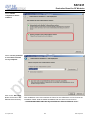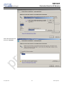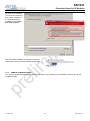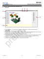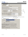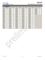
1
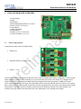
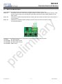
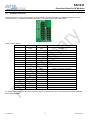
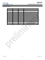
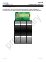
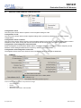
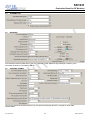
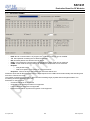
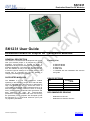
SK1231 Evaluation Board for RF Modules WIRELESS PRODUCTS SK1231 User Guide Evaluation board for Drop-In RF Transceiver Modules GENERAL DESCRIPTION The SK1231 is an advanced development tool to kick start your wireless project. It is powered by a strong STM32F4 microcontroller to support all kinds of applications what gives the developer high flexibility for possible applications. The board can be controlled via GUI, this software is easy to use and offers a fast way to find the right RF settings for a specific device. The second way of controlling the DP1231 Module is changing and debugging the firmware Packing List SUPPORTED MODULES DEVICE OPTIONS The DP1231 is a low cost transceiver module operating in the frequency ranges from 290-340 MHz, 424-510, 862-1020 MHz. The DP1231 is optimized for High Link Budget and for very small form factor. It incorporates a baseband modem with data rates up to 300 kb/s. Data handling features include a 66 byte FIFO, packet handling, automatic CRC generation and data whitening. All major RF communication parameters are programmable and most of them may be dynamically set. It complies with European (ETSI EN 300-220 V2.1.1) and North American (FCC part 15) regulatory standards. Part Version 02 preliminary - 2x EM1200 Board 2x EM1231 Board 2x Antennas 2x USB cable 1x CDROM with the installation files and the user guide SK1231C315 SK1231C433 SK1231C868 SK1231C915 Frequency band 290 - 340 MHz 424 - 510 MHz 862 - 902 MHz 902 - 1020 MHz RECOMMENDED READING - 1 Datasheet for DP1231 Datasheet for Semtech SX1231 www.anylink.de [email protected] SK1231 Evaluation Board for RF Modules WIRELESS PRODUCTS Table of Contents 1 2 EVALUATION BOARD OVERVIEW ......................................................................................... 3 1.1 Power supply options ........................................................................................................................................ 3 1.2 Button and LED description .............................................................................................................................. 4 1.3 RF-Module Connector ....................................................................................................................................... 5 1.4 MCU debugger/programmer ............................................................................................................................. 7 GETTING STARTED................................................................................................................. 8 2.1 STANDALONE MODE ...................................................................................................................................... 8 2.2 SAVING SETTINGS ON THE STARTERKIT ................................................................................................... 8 2.2.1 Save Register Setting on the Starterkit ..................................................................................................... 8 2.2.2 Load Register Setting on the Starterkit ..................................................................................................... 8 2.3 3 SOFTWARE INSTALLATION ........................................................................................................................... 8 2.3.1 EM12xx USER INTERFACE ..................................................................................................................... 8 2.3.2 EM1200 DRIVER SETUP ......................................................................................................................... 9 2.3.3 SAMPLE CONFIGURATIONS ................................................................................................................ 12 DP1231 USER INTERFACE DESCRIPTION .......................................................................... 13 3.1 OVERVIEW ..................................................................................................................................................... 13 3.2 SAVE AND LOAD REGISTER CONFIGURATIONS ...................................................................................... 14 3.3 COMMON ........................................................................................................................................................ 14 3.4 TRANSMITTER ............................................................................................................................................... 15 3.5 RECEIVER ...................................................................................................................................................... 15 3.6 PACKAGE FORMAT ....................................................................................................................................... 15 3.7 PACKET HANDLING ...................................................................................................................................... 16 3.8 TEMPERATURE SENSOR ............................................................................................................................. 16 3.9 REGISTERS.................................................................................................................................................... 17 3.10 DATA PROCESSING ...................................................................................................................................... 18 © Anylink 2014 2 www.anylink.de SK1231 Evaluation Board for RF Modules WIRELESS PRODUCTS 1 EVALUATION BOARD OVERVIEW 1: Power Supply 2: Reset 3: RF-Module 4: MCU debugger/programmer (ST-LINK/V2) 5: CAN (software not implemented) 6: LED indicator 7: USB / Full Speed 8: GPIO Buttons 9: RS232 (software not implemented) 10: Power via USB (only for power) 1.1 Power supply options Configure the jumper as the red marks show it. USB/ FS (7) Separate USB only for power (10) Extern 5 – 12 V The three pin header on the left side enable the user to setup the wanted power supply configuration. The pin header with the marking FS/HS decides if USB /FS (7) or power via USB (10) is used. If the Jumper (1) is plugged on the upper to pins Power is supplied from USB/FS (7) and if plugged on the lower pins power via USB (10) is used. For an external power supply the upper three pin header (3) has to be used marked with the red arrow. The marking BAT+ show the pin for positive power and the other two are grounded and can be used for the negative power supply. If this option is selected the three pin header (2) below has to be fitted with a jumper in the upper position. The marking on this pin header show USB / BAT for the two USB options or the external power supply. © Anylink 2014 3 www.anylink.de SK1231 Evaluation Board for RF Modules WIRELESS PRODUCTS 1.2 Button and LED description The evaluation board EM1200 has several buttons to interact with the firmware running on it. Button S1: The button saves the current running register setting for the RF chip to the MCU flash memory. If the board is reset by power off or pressing the reset button the MCU load the register setting from the flash memory. Button S2: This button is switching manually between master and slave modes see stand alone mode (Chapter 2.) for more details. Button S3: Initialization of a default register setting for the RF Chip in the GUI this function is called recommended settings. Furthermore the board has four LEDs to indicate RF processing and present USB connection. LED RED: RF missed packet LED GREEN1: RF data packet transmit LED GREEN2: RF data packet received LED GREEN3: USB is active © Anylink 2014 4 www.anylink.de SK1231 Evaluation Board for RF Modules WIRELESS PRODUCTS 1.3 RF-Module Connector The RF-Module connector is the interface to the RF-Modul. The Modul is held by an adaptor PCB that fit into the connector socket. For detailed information about the pinout have a look at the Tables below. Table of 20 Pin Socket: Pin no.: MCU GPIO DP1231 Description 1 PC10 SCK SPI clock 2 - VDD power supply VDD_MOD 3 PC12 MOSI SPI master out slave in 4 - GND power supply GND 5 PD3 DIO1 Digital I/O, software configured 6 PD2 DIO3 Digital I/O, software configured 7 PA15 NSS SPI chip select 8 PC11 MISO SPI master out slave in 9 PD5 DIO5 Digital I/O, software configured 10 PD4 RESET Manual reset 11 PD7 DIO4 Digital I/O, software configured 12 PD6 DIO0 Digital I/O, software configured 13 PE2 NC not connected 14 PB4 NC not connected 15 PE4 RXTX Indicator for RX or TX mode 16 PE3 NC not connected 17 PE6 DIO2 Digital I/O, software configured 18 PE5 NC not connected 19 PC14 NC not connected 20 PC13 NC not connected For the DP1231 Module just the 20 Pin socket is used for communication. The 14 Pin Socket is for further Modules and possible updates. © Anylink 2014 5 www.anylink.de SK1231 Evaluation Board for RF Modules WIRELESS PRODUCTS Table of 14 Pin Socket: © Anylink 2014 Pin no.: MCU GPIO DP1231 Description 1 2 3 4 5 6 7 8 9 10 11 12 13 14 PB7 PB6 - NC NC NC NC NC NC NC NC NC NC NC NC NC NC I2C SDA (optional) power supply VDD_ANA I2C SCL (optional) power supply GND not connected not connected not connected not connected not connected not connected not connected power supply GND not connected power supply VDD_FEM 6 www.anylink.de SK1231 Evaluation Board for RF Modules WIRELESS PRODUCTS 1.4 MCU debugger/programmer The debugger/programmer connector is the standard shipped with the ST-Link/v2. It allows the user to reprogram the microcontroller with its own custom firmware and also test the firmware that comes with the EM1200. The microcontroller code is open and can be flashed from a free IDE (COOCOX CoIDE) that is easy to install and run. © Anylink 2014 Pin no.: ST-LINK/V2 EM1200 1 2 3 4 5 6 7 8 9 10 11 12 13 14 15 16 17 18 19 20 VAPP VAPP TRST GND TDI GND TMS_SWDIO GND TCK_SWCLK GND NC GND TDO_SWO GND NRST GND NC GND VDD GND VDD NC GND GND GND GND SWDIO GND SWCLK GND NC GND SWO GND NRST GND NC GND NC GND 7 www.anylink.de SK1231 Evaluation Board for RF Modules WIRELESS PRODUCTS 2 2.1 GETTING STARTED STANDALONE MODE The stand alone mode is applied if power supply is connected and no USB connection is present. USB connection is indicated by the flashing led GREEN3 “no Flashing = no Data transfer”. In the Stand alone mode the device is programmed to work as Master device and transmitting data packets with a PING signature but also set itself in receive mode between the transmitting. If another Master device is present transmitting PING messages the first device to receive a PING switch in Slave mode Transmitting PONG messages. Switching between Master and Slave mode can also be done by pressing the s2 button. If a Master and Salve configuration is present the Master sends PING to Slave and is answered with PONG. As long as the Master is getting no PONG massage the RED LED is flashing. The LED GREEN1 show transmit and GREEN2 show receiving. Pressing button S1 will save the current RF setting on the EM1200 device. This setting is applied at every reset and power on reset. Even a long power off - power on is not deleting the saved settings. Just a new saving event can overwrite the old settings, because they are saved in the microcontroller flash memory. Pressing button S3 sets all RF setting to the software defined defaults equal to the GUI function Recommended Settings 2.2 SAVING SETTINGS ON THE STARTERKIT Having the ability to save different register settings on the Starter kit, can be a very helpful tool for every Developer. That for the EM1200 Start kit is able to save four different register setting for the RF Chip. This Setting can be accessed via the buttons during the startup procedure after every Reset event. 2.2.1 Save Register Setting on the Starterkit Start with creating a setting with the graphical user interface. If the GUI shows the right settings there is two ways how to save this setting. One is to use the “Save on device” function in the “Configuration” menu. Simply press it and watch the RED LED light up for a second. Now you saved the setting in position one to use a differed position press S3 while the RED LED is on and it jumps to GREEN1, GREEN2 and GREEN3. Every LED stands for a different save position. Saving at the same position twice overnights the old register setting. Second way to save is to press the Save button S1, the RED LED will also light up for a second with mean you saved at first position. Keeping the button S1 pressed and shortly pressing button S3 and you change the save position. 2.2.2 Load Register Setting on the Starterkit Loading the saved Register setting is done automatically in the reset procedure. Save position one (RED LED) is default and can be changed by pressing button S3 while the RED LED is on. The other LEDs will light up one after another, if you reached the required position just let it finish start up and you done. 2.3 SOFTWARE INSTALLATION 2.3.1 EM12xx USER INTERFACE Software installation on Windows 7. The installation media also contains also the Microsoft Visual Studio 2005 C Runtime that must be installed on the target computer. Installation can be started by running “vcdredist_x86/vcdredist_x86.exe” on the installation media. To install the User Interface starting the “EM1200 Software.msi” that can be found on the installation media. © Anylink 2014 8 www.anylink.de SK1231 Evaluation Board for RF Modules WIRELESS PRODUCTS 2.3.2 EM1200 DRIVER SETUP The driver can only be installed while the EM1200 is connected. The driver must be installed using the device manager. The device manager can be started from the Windows Start menu by running the command “devmgmt.msc” The EM1200 Board identifies itself as USB Input device. The EM1200 can be identified with the following Hardware ID’s. © Anylink 2014 9 www.anylink.de SK1231 Evaluation Board for RF Modules WIRELESS PRODUCTS Select “Brows computer for driver software” Select “Let me pick from a list of device drivers on my computer” Click on the “Hard disk” Button and brows to the EM1200 driver directory. © Anylink 2014 After installation of the User Interface the Driver for the USB Device can be found in the Installation Folder. With the default installation Path the driver can be found in. “%PROGRAMFILES%\ANYLINK Systems\EM1200 Software\EM1200 driver” 10 www.anylink.de SK1231 Evaluation Board for RF Modules WIRELESS PRODUCTS Select the EM1200 driver and click “Continue” © Anylink 2014 11 www.anylink.de SK1231 Evaluation Board for RF Modules WIRELESS PRODUCTS As the driver is unsigned, you will receive a warning during driver installation. To continue the driver installation click “Install this driver anyway”. After successful installation of the driver, the device should show up in the Device Manager as EM1200. 2.3.3 SAMPLE CONFIGURATIONS You can find sample configurations for different applications of the modules in the installation directory and on the installation media. © Anylink 2014 12 www.anylink.de SK1231 Evaluation Board for RF Modules WIRELESS PRODUCTS 3 3.1 DP1231 USER INTERFACE DESCRIPTION OVERVIEW 1. Connect Button – Blue indicates that the EM1200 is connected Gray indicates that the EM1200 is disconnected. 2. Settings Menu – Allows saving and loading of register settings. 3. Monitor Button – Enables/Disable register monitoring, if enabled all readable Register values are continually read from the module and the user interface is updated according to this values. 4. Documentation shortcuts can be found in this Dropdown menu 5. Configuration Sections – Gives access to the different configuration options for the module the first click will display the specified section, a second click will move the configuration options in a separate window. 6. Information – Gives information about the current selected configuration element. 7. Operation Mode and Interrupt Monitoring – Monitoring must be enabled © Anylink 2014 13 www.anylink.de SK1231 Evaluation Board for RF Modules WIRELESS PRODUCTS 3.2 SAVE AND LOAD REGISTER CONFIGURATIONS Configuration->Save This menu point can be used to export the current register settings to a file. Configuration->Load This menu point can be used to restore register settings from a previously saved file or one of the example configurations. Configuration->Save on Device This menu point can be used to save the current register settings on the device. The saved settings will be used in standalone mode. When testing with the EM1200 boards both should be set to the same configuration. Configuration->Reset Registers->Recommended Reset the Registers to the firmware default values. It might be necessary to change the Carrier frequency as the Software cannot distinguish between the Frequency variants of the used module. Configuration->Reset Registers->Power ON The Registers will be reset to the SX1231 Power ON Default values as listed in the Datasheet. 3.3 COMMON In the common settings section it is possible to change - Carrier frequency - Bitrate - Modulation type - Modulation Parameters FSK and OOK © Anylink 2014 14 www.anylink.de SK1231 Evaluation Board for RF Modules WIRELESS PRODUCTS 3.4 TRANSMITTER Here the transmitter settings can be changed. 3.5 RECEIVER This subsection allows modification of the LNA-, RX filter-, RSSI- (Receive Signal Strength Indicator), AFC(Automatic Frequency Cancelation) settings. 3.6 PACKAGE FORMAT This section describes the packet format e.g. the criteria for package detection, acceptance, CRC, data representation. © Anylink 2014 15 www.anylink.de SK1231 Evaluation Board for RF Modules WIRELESS PRODUCTS 3.7 PACKET HANDLING In this section the Listen Mode and Auto Mode can be configured. Also the timeout values for Packet reception can be configured here. Using these autonomous chip operation modes is recommended for applications that require energy efficient operation. 3.8 TEMPERATURE SENSOR This section gives access to the temperature sensor embedded in the SX1231. © Anylink 2014 16 www.anylink.de SK1231 Evaluation Board for RF Modules WIRELESS PRODUCTS 3.9 REGISTERS Here the raw register values of the SX1231 can be read and written. © Anylink 2014 17 www.anylink.de SK1231 Evaluation Board for RF Modules WIRELESS PRODUCTS 3.10 DATA PROCESSING The RF communication can be tested here, the following modes are supported: - IDLE: No RF communication is in progress, the TX Buffer on the µC can be modified. - TX: Send packets containing the TX Buffer as payload. - RX: Received packets are stored in the RX Buffer. - PING: in this mode the Communication in Standalone master mode can be observed. - PONG: in this mode the Communication in Standalone slave mode can be observed. - Request: o One packet is sent o Wait for reception of one packet or a receive timeout. - Response: After receiving a valid packet the TX Packet will be sent Please be aware that for Request/Response the time required for the USB Communication delays the switching time from RX to TX and vice versa. The register monitoring may disturb the firmware when handling larger payload sizes and higher bitrates. The monitoring should be disabled in this case. Restriction on the Firmware: - Continuous Mode is not supported. - Unlimited length package format is not supported. - Listen mode/Auto mode are not supported. - Packet format without Syncword recognition is not supported. © Anylink 2014 18 www.anylink.de SK1231 Evaluation Board for RF Modules WIRELESS PRODUCTS © Anylink 2014 All rights reserved. Reproduction in whole or in part is prohibited without the prior written consent of the copyright owner. The information presented in this document does not form part of any quotation or contract, is believed to be accurate and reliable and may be changed without notice. No liability will be accepted by the publisher for any consequence of its use. Publication thereof does not c onvey nor imply any license under patent or other industrial or intellectual property rights. Anylink assumes no responsibility or liability whatsoever for any failure or unexpected operation resulting from misuse, neglect improper installation, repair or improper handling or unusual physical or electrical stress including, but not limited to, exposure to parameters beyond the specified maximum ratings or operation outside the specified range. ANYLINK PRODUCTS ARE NOT DESIGNED, INTENDED, AUTHORIZED OR WARRANTED TO BE SUITABLE FOR USE IN LIFE-SUPPORT APPLICATIONS, DEVICES OR SYSTEMS OR OTHER CRITICAL APPLICATIONS. INCLUSION OF ANYLINK PRODUCTS IN SUCH APPLICATIONS IS UNDERSTOOD TO BE UNDERTAKEN SOLELY AT THE CUSTOMER’S OWN RISK. Should a customer purchase or use Anylink products for any such unauthorized application, the customer shall indemnify and hold Anylink and its officers, employees, subsidiaries, affiliates, and distributors harmless against all claims, costs damages and attorney fees which could arise. Version 01 preliminary 02 preliminary 03 preliminary Create Date: 03.11.14 18.12.14 19.12.14 Creator Changes Create new Datasheet Update with new Details Update with new Details Contact Information: Anylink Systems AG Ringlerstrasse 19 85057 Ingolstadt Germany Phone (+49) 841-881-1200 Fax: (+49) 841-881-1201 © Anylink 2014 19 www.anylink.de