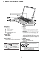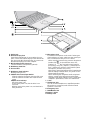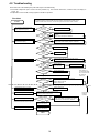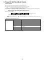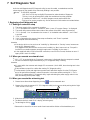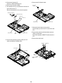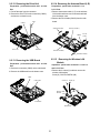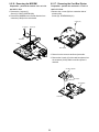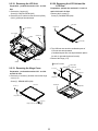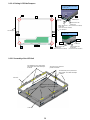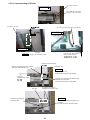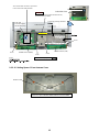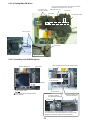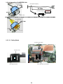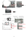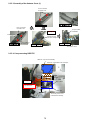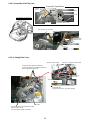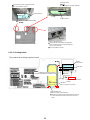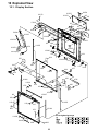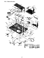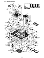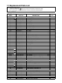
1
ORDER NO. CPD0610204C1㩷
Personal Computer
CF-W5
This is the Service Manual for
the following areas.
M …for U.S.A. and Canada
Model No. CF-W5LWEZZ1 2
1: Operation System
B: Microsoft® Windows® XP Professional
2: Area
M: Refer to above area table
© 2006 Matsushita Electric Industrial Co., Ltd. All rights reserved.
Unauthorized copying and distribution is a violation of law.
WARNING
For U.K.
This apparatus must be earthed for your safety.
To ensure safe operation the three-pin plug must be inserted only into a standard three-pin power point
which is effectively earthed through the normal household wiring.
Extension cords used with the equipment must be three-core and be correctly wired to provide connection to earth. Wrongly wired extension cords are a major cause of fatalities.
The fact that the equipment operates satisfactorily does not imply that the power point is earthed and
that the installation is completely safe.
For your safety, if you have any doubt about the effective earthing of the power point, consult a qualified electrician.
FOR YOUR SAFETY PLEASE READ THE FOLLOWING TEXT CAREFULLY
This appliance is supplied with a moulded three pin mains plug for your safety and convenience.
A 3 amp fuse is fitted in this plug.
Should the fuse need to be replaced please ensure that the replacement fuse has a rating of 3 amps and
that it is approved by ASTA or BSI to BS 1362.
Check for the ASTA mark
or the BSI mark
on the body of the fuse.
If the plug contains a removable fuse cover you must ensure that it is refitted when the fuse is replaced.
If you lose the fuse cover the plug must not be used until a replacement cover is obtained.
A replacement fuse cover can be purchased from your local Panasonic Dealer.
IF THE FITTED MOULDED PLUG IS UNSUITABLE FOR THE SOCKET OUTLET IN YOUR
HOME THEN THE FUSE SHOULD BE REMOVED AND THE PLUG CUT OFF AND DISPOSED
OF SAFELY.
THERE IS A DANGER OF SEVERE ELECTRICAL SHOCK IF THE CUT OFF PLUG IS INSERTED
INTO ANY 13 AMP SOCKET.
If a new plug is to be fitted please observe the wiring code as shown below.
If in any doubt please consult a qualified electrician.
Warning: THIS APPLIANCE MUST BE EARTHED.
Important
The wires in this mains lead are coloured in accordance with the following code:
Green-and-yellow:
Earth
Blue:
Neutral
Brown:
Live
As the colours of the wires in the mains lead of this apparatus may not correspond with the coloured
markings identifying the terminals in your plug, proceed as follows:
The wire which is coloured GREEN-and-YELLOW must be connected to the terminal in the plug
coloured GREEN or GREEN-andwhich is marked by the letter E or by the safety earth symbol
YELLOW.
The wire which is coloured Blue must be connected to the terminal which is marked with the letter N or
coloured BLACK.
The wire which is coloured Brown must be connected to the terminal which is marked with the letter L
or coloured RED.
The mains plug on this equipment must be used to disconnect the mains power.
Please ensure that a socket outlet is available near the equipment and shall be easily accessible.
How to replace the fuse
Open the fuse compartment with a screwdriver and replace the fuse.
Warnings
This equipment is not designed for connection to an IT power system.
(An IT system is a system having no direct connections between live parts and Earth; the exposed-conduciveparts of the electrical installation are earthed.
An IT system is not permitted where the computer is directly connected to public supply systems in the U.K.)
Disconnect the mains plug from the supply socket when the computer is not in use.
This equipment is produced to BS800/1983.
2
LASER SAFETY INFORMATION
For U.S.A.
Class 1 LASER-Product
This product is certified to comply with DHHS Rules 21 CFR Subchapter J.
This product complies with European Standard EN60825 (or IEC Publication 825)
For all areas
This equipment is classified as a class 1 level LASER product and there is no hazardous LASER radiation.
Caution:
(1) Use of controls or adjustments or performance of procedures other than those specified herein may result in
hazardous radiation exposure.
(2) The drive is designed to be incorporated into a computer-based system or unit which has an enclosing cover.
It should never be used as a stand alone drive.
Danger:
The serviceman should not remove the cover of drive unit and should not service because the drive unit is a nonserviceable part.
Please check DANGER label on PD-drive unit.
Unplug the AC power cord to the equipment before opening the top cover of the drive.
When the power switch it on, do not place your eyes close to the front panel door to look into the interior of the unit.
LASER Specification
Class 1 level LASER Product
Wave Length: DVD 658–8 nm
CD 775~815 nm
Laser safety information is appropriate only when drive with laser is installed.
3
4
5
CONTENTS
1. Specifications
7
2. Names and Functions of Parts
10
3. Block Diagram
12
4. Diagnosis Procedure
13
5. Power-On Self Test (Boot Check)
15
6. List of Error Codes <Only when the port replicator is connected>
16
7. Self Diagnosis Test
18
8. Wiring Connection Diagram
23
9. Disassembly/Reassembly
24
10. Exploded View
86
11. Replacement Parts List
89
1 Specifications
7
8
9
2 Names and Functions of Parts
A :Function Key
B :Keyboard
C :LED Indicator
: Caps lock
: Numeric key (NumLk)
: Scroll lock (ScrLk)
: Hard disk drive status
ECO : Economy Mode (ECO) status
: Battery status
D :Power Switch
Power Indicator
Off: Power off/Hibernation
Green: Power on
Blinking green: Standby
E : Wireless Switch
<Only for model with wireless LAN/wireless WAN>
F : Touch Pad
G :LCD
H :Speaker
I : LAN Port
If the Mini Port Replicator is connected to the computer,
connect the LAN cable to the LAN port on the Mini Port
Replicator. You cannot use the LAN port on the computer.
J : Modem Port
Be sure to use the included modem telephone cable,
and insert the end of the cable with the phyllite core
into the modem port on the computer.
K :Security Lock
You can connect a Kensington cable. Refer to the instruction manual of the cable. The security lock and cable is a
theft prevention device. Matsushita Electric Industrial Co.,
Ltd. will bear no responsibility in the event of theft.
L : USB Ports
M :Wireless LAN Antenna
<Only for model with wireless LAN>
N :CD/DVD Drive
CAUTION
Wireless WAN Antenna
When closing the disk
cover, press down
near the drive power/
open switch (position
of the arrow) to
ensure that the cover
is locked.
For model with EVDO or without wireless WAN:
The SIM card slot under this cover is not used for
this model. Do not open the cover.
For other models:
Refer to the additional instructions.
10
EXT.
M
N
A :DC-IN Jack
B :External Display Port
If the Mini Port Replicator is connected to the computer, connect the external display to the external display port on the Mini Port Replicator. You cannot use
the external display port on the computer.
C :Mini Port Replicator Connector
Connect the Mini Port Replicator (optional).
D :SD Memory Card Slot
E : PC Card Slot
F : SD Memory Card Indicator
Blinking: During access
G :CD/DVD Drive Power/Open Switch
Slide the switch to the right to open the disk cover.
Slide the switch to the left to turn on/off the drive
power.
CD/DVD Drive Indicator
Off: Drive power is off.
Green: Drive power is on, but the drive is not
accessed.
Blinking green: Drive power is on, and the drive is
being accessed.
H :Microphone Jack
A condenser microphone can be used. If other types
of microphones are used, audio input may not be possible, or malfunctions may occur as a result.
When recording in stereo using a stereo microphone:
Double-click
in the notification area, click
[Options] - [Properties], and add a check mark for
[Recording], click [OK] - [Options] - [Advanced Controls] - [Advanced], remove a check mark for [Mono
Microphone], and then click [Close].
When using a monaural microphone with a 2-terminal plug:
With the settings outlined above, only audio on the
left track will be recorded.
When monitoring the microphone audio using headphones, sounds on the left track cannot be heard,
regardless of the above settings. This is a result of the
computer s specifications, and is not a malfunction.
I : Latch
J : Headphone Jack
You can connect headphones or amplified speakers.
When they are connected, audio from the internal
speakers is not heard.
K :Emergency Hole
L : RAM Module Slot
M :Battery Latches
N :Battery Pack
11
3 Block Diagram
12
4 Diagnosis Procedure
4.1. Basic Procedures
13
4.2. Troubleshooting
Please take note of the following two points with regard to troubleshooting:
1. Know-how of diagnosis upon occurrence of heavy troubles, e.g. Set cannot be turned ON , Set fails to start , No display on
screen , etc.
2. Explanation of each trouble, mainly symptom of trouble in operation.
Flow Chart
START
START
Set cannot be supplied with current.
Power lamp fails to light up.
Pay attention to the following points when in pursuit of the cause of a troubleshooting.
1. Peripheral apparatus connected with the set should all be removed before operation check.
2. Make sure that cables, boards, etc. are not coming off, and recheck the contact condition.
NG
AC
Adaptor/Battery
Output voltage
Replace AC Adaptor/Battery
OK
NO
Power lamp
check
YES
Dark display on screen.
Screen fails to display.
NG
Inverter board
Check contact condition of power input terminal. Replace if
defective.
Check Power SW. Replace if defective.
Replace inverter board.
Check inverter cable continuity. Replace if defective
OK
NO
LCD back
light lighting
YES
NG
LCD unit
check
Replace LCD back light.
Replace LCD unit.
OK
Failure in starting
NO
BIOS operation
check
Replace main board (Check fuse at power source).
YES
NG
Result of
POST
OK
NG
Set-up utility
starting
Refer to POST
error code table.
Replace main board.
Replace main board.
OK
Return set-up utility setpoint to the state of delivery from factory .
NO
HDD access
YES
Not displayed properly on screen.
NG
Main board
check
Heavy trouble e.g.,
Set cannot be turned
ON , Set fails to start ,
No display on
screen , etc.
Check HDD cable connection and continuity.
Replace if defective.
Replace HDD & Reinstall.
Replace main board.
Replace main board
OK
Some or all keys cannot be input.
DVD/CD CALL not practicable.
Make sure of contact of K/B connector in use.
Replace keyboard or main board.
NO
Trouble
symptoms on some
of DVD or CD
YES
*Clean DVD-ROM drive with an applicator.
Replace DVD drive.
Replace main board.
Starts but operates unstably.
Reinstall HDD.
Replace main board.
START
END
14
Check if there are any flaws on DVD or CD
media. Since flaws may appear on specific
media, DVD or CD media can be defective.
Each kind of
trouble in
operation.
5 Power-On Self Test (Boot Check)
Outline of POST
The set has a boot check function called POST (Power-On Self Test) in it.
The condition of the main body is diagnosed by checking beep sound or error code.
Start .............Test begins automatically when power switch is set to ON.
Normal finish .....After memory checking, a beep sound is issued once and the set is placed into automatic stop.
Note: If no error occurs, nothing is displayed. (No display of OK, etc.)
Error Diagnosis by Checking Beep Signal Sound
The beep sound is as follows:
(1 (long sound) -2-3-4)
(Length of bar shows length of sound.)
= long sound (about 0.4 sec.),
= short sound (about 0.2 sec.), Length between sounds is about 0.1 sec.
Table of errors classified by beep sounds
Diagnosis
Main board
Beep signal sound
Error message
1(long sound)-2
BIOS ROM error
1-2-2-3
BIOS ROM error
1-3-1-1
RAM error
1-3-1-3
Keyboard controller error
1-3-4-1
RAM error
1-3-4-3
RAM error
1-4-1-1
RAM error
2-1-2-3
BIOS ROM error
2-2-3-1
Occurrence of unexpected offering
(Note) A beep sound is also issued in case of other I/O trouble.
15
6 List of Error Codes <Only when the port replicator is connected>
The following is a list of the messages that BIOS can display. Most of them occur during
POST. Some of them display information about a hardware device, e.g., the amount of memory
installed. Others may indicate a problem with a device, such as the way it has been configured.
Following the list are explanations of the messages and remedies for reported problems.
If your system displays one of except the messages marked below with an asterisk (*), write
down the message and contact Panasonic Technical Support. If your system fails after you
make changes in the Setup menus, reset the computer, enter Setup and install Setup defaults
or correct the error.
0200 Failure Fixed Disk
Fixed disk in not working or not configured properly. Check to see if fixed disk is attached
properly. Run Setup. Find out if the fixed-disk type is correctly identified.
0210 Stuck key
Stuck key on keyboard.
0211 Keyboard error
Keyboard not working.
0212 Keyboard Controller Failed
Keyboard controller failed test. May require replacing keyboard controller.
0213 Keyboard locked - Unlock key switch
Unlock the system to proceed.
0230 System RAM Failed at offset : nnnn
System RAM failed at offset nnnn of in the 64k block at which the error was detected.
0231 Shadow RAM Failed at offset : nnnn
Shadow RAM failed at offset nnnn of the 64k block at which the error was detected.
0232 Extended RAM Failed at offset : nnnn
Extended memory not working or not configured properly at offset nnnn.
0250 System battery is dead - Replace and run SETUP
The CMOS clock battery indicator shows the battery is dead. Replace the battery and run Setup
to reconfigure the system.
*0251 System CMOS checksum bad - Default configuration used
System CMOS has been corrupted or modified incorrectly, perhaps by an application program
that changes data stored in CMOS. The BIOS installed Default SETUP Values. If you do not
want these values, enter Setup and enter your own values. If the error persists, check the system
battery or contact Panasonic Technical Support.
0260 System timer error
The timer test failed. Requires repair of system board.
0270 Real time clock error
Real-time clock fails BIOS test. May require board repair.
*0280 Previous boot incomplete - Default configuration used
Previous POST did not complete successfully. POST loads default values and offers to run
Setup. If the failure was caused by incorrect values and they are not corrected, the next boot
will likely fail. On systems with control of wait states, improper Setup settings can also terminate POST and cause this error on the next boot. Run Setup and verify that the wait-state
configuration is correct. This error is cleared the next time the system is booted.
0281 Memory Size found by POST differed from EISA CMOS
Memory size found by POST differed from EISA CMOS.
16
17
Troubleshooting
02D0 System cache error - Cache disabled
Contact Panasonic Technical Support.
02F0: CPU ID:
CPU socket number for Multi-Processor error.
02F4: EISA CMOS not writable
ServerBIOS2 test error: Cannot write to EISA CMOS.
02F5: DMA Test Failed
ServerBIOS2 test error: Cannot write to extended DMA (Direct Memory Access) registers.
02F6: Software NMI Failed
ServerBIOS2 test error: Cannot generate software NMI (Non-Maskable Interrupt).
02F7: Fail - Safe Timer NMI Failed
ServerBIOS2 test error: Fail-Safe Timer takes too long.
device address Conflict
Address conflict for specified device.
Allocation Error for: device
Run ISA or EISA Configuration Utility to resolve resource conflict for the specified device.
Failing Bits : nnnn
The hex number nnnn is a map of the bits at the RAM address which failed the memory test.
Each 1 (one) in the map indicates a failed bit. See error 230,231 or 232 for offset address of the
failure in System, Extended or Shadow memory.
Invalid System Configuration Data
Problem with NVRAM (CMOS) data.
I/O device IRQ conflict
I/O device IRQ conflict error.
Operating System not found
Operating system cannot be located on either drive A: or drive C:. Enter Setup and see if fixed
disk and drive A: are properly identified.
Parity Check 1 nnnn
Parity error found in the system bus. BIOS attempts to locate the address and display it on the
screen. If it cannot locate the address, it displays ????. Parity is a method for checking errors
in binary data. A parity error indicates that some data has been corrupted.
Parity Check 2 nnnn
Parity error found in the I/O bus. BIOS attempts to locate the address and display it on the
screen. If it cannot locate the address, it displays ????.
Press <F1> to resume, <F2> to Setup
Displayed after any recoverable error message. Press <F1> to start the boot process or <F2> to
enter a Setup and change the settings. Write down and follow the information shown on the
screen.
7 Self Diagnosis Test
As for the self-diagnosis test(PC-Diagnostic utility) to use this model, a standard test and the
enhancing test by the module of the main body building in are possible.
Notes To skip BIOS password
Use <Ctrl>+<F10> key to skip BIOS password or authentication of fingerprint.
This key is only for entering DIAG mode. Not available to boot the computer.
If customer set "HDD Lock", the DIAG program cannot perform HDD test.
*This key is for service purpose only. Do not disclose this information to unrelated others.
1. Beginning of self-diagnosis test
1-1. Setting of content of setup
1.
2.
3.
4.
The power supply of the computer is turned on.
" F2 " is pushed on the screen of "Panasonic" while " press <F2 to enter Setup> " is displayed.
The setup utility starts and then takes notes of the content of the BIOS setup of present set.
" F9 " is pushed, " Yes" is selected on the screen of " Is the default value loaded? ", and " Enter"
is pushed.
5. " F10 " is pushed.
6. " Yes" is selected on the screen of the setup confirmation, and " Enter" is pushed.
7. The computer starts automatically.
Attention
If the device which can be set is set to "Invalidity" by "Advanced" or "Security" menu, becomes an
error by "PC-Diagnostic utility".
(It is judged that the device which can be set to "Invalidity" by "Main" menu such as "Flat pad" is
normal if the controller operates normally though sets to "Invalidity" by the setup. )
In the model with built-in DVD of the USB connection, even if DVD is normal, becomes an error if
legacy USB is set to "Invalidity"
1-2. When you execute an automatic test
1. "Ctrl" + "F7" is pushed while the "Panasonic" start screen is displayed after the computer is started.
2. The test of all devices begins automatically by "PC-Diagnostic utility"’s starting.
Attention
It is a test which the customer who bought PC can execute. (As for HDD, the enhancing test is also
possible.)
A flat pad does not work for a while after starting "PC-Diagnostic utility".
The movement of a flat pad might become abnormal If after RAM begins from the CPU/System
test, a flat pad will be operated in about 30 seconds. In that case,restarts pushing"Alt" + "Ctrl" +
"Del" key. Or, please start "PC-Diagnostic utility" again after doing the power supply switch in the
slide, and turning off the power supply.
1-3. When you execute the enhancing test
1. Please let me discontinue diagnosing clicking
to end an automatic test.
2. Please click on the character of "D" "PC-Diagnostic utility" on the screen while pushing both of right
"Shift" and left "Shift" keys.
D
3. All devices which can select the enhancing test make the setting of the enhancing test possible.
4. The district device is made"FULL" display (enhancing test).
5. The test begins clicking
.
*Please refer to item 4 for the error result of each test and the division of the breakdown part.
18
2. Operation of PC-Diagnostic Utility
-Only the device which can be inspected on the entire screen is displayed.
-The item does not appear when the device of wireless LAN etc. is not physically connected.
-The movement of the item must use an arrow key or a flat pad.
-As for the device under the diagnosis, blue and yellow are alternately displayed at the left of the icon.
- The diagnosis result of the device greens at the left of the icon when it is normal, and becomes red when
abnormal.
-When the test of all devices ends, the test result is displayed under the right of the screen.
-Please click
while diagnosing when being stop on the way by the time the test of all devices ends.
-Please click
when you restart "PC-Diagnostic utility".
*Each device is tested from the beginning, and it is not possible to restart on the way.
19
2-1. Selection of tested device
-To test only a specific device, "Test" and "Do not test" of each device can be selected.
-The device which can select the enhancing test changes in order of "The standard is tested" and "Do not
test" whenever the device icon is clicked.
Do not test
Start the standard test
Please begin testing clicking
if the selection of the tested device ends.
2-2. "PC-Diagnostic utility" End method
When
of "Close" on the right of the screen is clicked, the computer reactivates automatically. Or, the
power supply switch is done in the slide and the power supply is turned off.
2-3. The content of the setup is returned to the setting of the user
1. Turned on the computer.
2. "F2" is pushed on the screen while "Press<F2>to enter Setup" is displayed of "Panasonic".
3. Push "F10", and on the screen of "Is the change in the setting preserved and do end?"and then "Yes"
is selected, and "Enter" is pushed.
4. The computer reactivates automatically.
5. The end option is chosen by the start menu, and the power supply of the computer is turned off.
Standard at test time
All devices other than RAM and HDD
RAM standard test
HDD standard test
HDD enhancing test (60GB)
about 1 minute
1 - 2 minutes
2 - 3 minutes
about 40 minutes
Ex.The standard when the standard <all device> is tested becomes 1+2+3=6 minutes.
There is greatly a difference from RAM test when the memory is increased according to the performance of the memory occasionally.
Moreover, when the main body of PC under the test is a high temperature, it occasionally takes time.
There is greatly a difference from HDD according to the performance of the drive occasionally.
20
7.1. Test Item and Division of trouble
Test item Stanard Enhancing
Content of standard test
Content of enhancing test
Place with possibility of breakdown
CPU /
SYSTEM
CPU is shifted to protected mode, and
"Violation of the paging", "Operation of
the violation of a privileged instruction", and DMA, INT, TIMER, and the
RTC operation are confirmed.
CPU /
Main board
RAM
All memory space is tested in a special memory access pattern based on
"R.S.T . technology".
Memory / Mainboard
HDD
The record area frequently accessed
with Microsoft Windows XP to test in
about two minutes regardless of
points of HDD is emphatically tested.
MODEM
It is confirmed not to find abnormality
in the AC97 modem controller.
MODEM/ Mainboard
Wireless
LAN
It is confirmed not to find abnormality
in the Wireless LAN modem controller.
Wireless LAN
board /
Connector /
Mainboard
All record area is tested.
HDD /
Mainboard /
Cable /
Connector
Sound *5
USB
It is confirmed not to find abnormality
in the USB controller.
It is confirmed not to find abMainboard /
normality in the wiring beConnector
tween the USB controller and
the connector by confirming
the connection of the USB
equipment connected with the
USB connector.
It is confirmed not to find abnormality
in the LAN controller.
It is confirmed not to find abnormality in the wiring between the controller and the
connector by connecting to
HUB with LAN cable.
*1
LAN
*2
Mainboard /
Connector
PC Card
It is confirmed not to find abnormality
in the CardBus controller.
Mainboard
SD
It is confirmed not to find abnormality
in the SD controller.
Mainboard
Mainboard /
Keyboard
Keyboard
*3
It is confirmed not to find abnormality The key is actually input, and
in keyboard controller’s keyboard inter- the operation is displayed on
the screen.
face.
Touch Pad
*4
Whether keyboard controller’s mouse The operation is actually dis- Mainboard /
played on the screen by oper- Touch Pad
interface operates normally is conating the touch pad.
firmed.
DVD-ROM
*6
The drive is normally reset, and it is
accessible is confirmed.
21
It is confirmed to be able to
read media normally.
Mainboard /
Touch Pad
Test Item
Standard Enhanced
Content of Standard Test
It is confirmed not to find
abnormality in the USB
connection of Touch Screen.
This test cannot find
abnormality of Touch Screen.
It is confirmed not to find
abnormality in the connection
of Main board and Bluetooth
module.
It is confirmed not to find
abnormality in the connection
of Main board and Wireless
WAN module.
It is confirmed not to find
abnormality in the legacy FD
drive.
This test cannot find
abnormality of mechanical
breakdown. (e.g.. Head, Motor)
It is confirmed not to find
abnormality in access to
VRAM with VESA.
The PC which uses main
memory as VRAM may fail with
main memory failure.
It is confirmed not to find
abnormality in the connection
of Main board and GPS
It is confirmed not to find
abnormality in the IEEE1394
controller.
Touch Screen
Bluetooth
Wireless WAN
Floppy
Video
GPS
IEEE1394
Perform Touch Screen
functionality practically.
Operator has to judge
PASS/FAIL with test result.
Smart Card
It is confirmed not to find
abnormality in the Smart Card
controller.
Serial Port
*7
It is confirmed not to find
abnormality of Super I/O
UART function.
This test cannot find lack of
wiring between Super I/O and
Serial Connector.
*8
It is confirmed not to find
abnormality of Super I/O
parallel function.
This test cannot find lack of
wiring between Super I/O and
Parallel Connector.
*1
*2
*3
*4
*5
The place with possibility of
breakdown
Main board/
Touch Screen
Bluetooth cable
WWAN cable
FD Drive/
Main board (Super I/O)/
FDD cable
FDD connector
Main board
(Chipset, Graphic
Controller)/
Memory
GPS cable
Main board
(IEEE#394 Controller)
It is confirmed not to find
abnormality in the wiring
between Chipset and Express
Card.
Express Card
Parallel Port
Content of Extend Test
Main board (Chipset)/
Express Card Connector
Main board
(Smart Card Controller)
It is confirmed not to find
abnormality in the wiring
between Super I/O and Serial
Connector.
This test cannot find failure of
cable characteristic and device
problems.
It is confirmed not to find
abnormality in the wiring
between Super I/O and
Parallel Connector.
This test cannot find failure of
cable characteristic and device
problems.
Main board (Super I/O)/
Serial Connector
Main board (Super I/O)/
Parallel Connector
Please connect the USB device with the port (USB connector) which wants to test before the tests.
Please connect LAN port with LAN HUB with LAN cable before the tests.
The operator actually inputs the key, and the operator judges PASS/FAIL of the test.
The operator actually operates the mouse, and the operator judges PASS/FAIL of the test.
It is not abnormal though the sound is emitted from the speaker while testing.
When the test result is PASS, trouble is thought by not hearing of the sound under the test from
the speaker and the headphone by the wiring of the audio output system.
*6 Please set DVD/CD media in the drive before the tests.
*7 Please set a Special Loop Back Connector Tool at serial connector for Enhanced Test.
(This Connector Tool is same as the one used before.)
*8 Please set a Special Loop Back Connector Tool at parallel connector for Enhanced Test.
(This Connector Tools is same as the one used before.)
22
8 Wiring Connection Diagram
Connection by Cable
Connection Cable
1
PAD FFC
2
DRIVE FFC
3
LCD Cable
4
LAN Cable
5
MODEM Cable
6
MAIN SUB Cable
7
DC-IN Cable
8
SP Cable
9
Antenna PCB-L
10
Antenna PCB-R
11
PCB,HDD FPC UNIT
12
WM Cable
Direct connection Connectors
Parts on Bottom Side
Antenna Board
(R)
LCD
DFJK12U112BB
DFJK9000ZA
DFJS957ZA
DFJS979ZA
DFJ959ZC
DFJS960ZA
DFJS1020YA
DFJS962ZA
N1ZYYY000002
N1ZYYY000001
DL3UP1443AAA
DFJS1048ZA
WWAN Antenna Board
(R)
̪10
CN1501
Wireless
LAN Module
Battery Pack
̪12
WWAN
SIMM
Card
Speaker
̪9
WWAN Antenna Board
(L)
Antenna Board
(L)
Inverter Board
Keyboard
̪8
CN601
CN26
VGA
CN10
CN15
CN11
CN12
DC IN
Main Board
CN2
̪7
CN28
MDC MODEM
̪5
HDD
̪11
CN4
CN19
CN600
CN18
̪6
CN23
USB Board
CN903 USB
CN25
CN13
SD Card
CN902 USB
CN901
̪2
CD-RW,DVD-ROM Drive
CN14
CN16
CN3
CN21
PCMCIA
Slot
JK2
̪4
JK1
SW Board CN951
SW6
SW7
POWER SW W-LAN
ON/OFF SW
Headphone
Mic
Lithium Battery
̪1
̪4
DIMM memory
(Option)
LAN
Touch Pad
CF-BAW0512U
(PC2-4200)
23
SW951
Open SW
9 Disassembly instructions
9.1. Disassembly Flow Chart
Main Unit
9.2.1.
Preparation
1. End the Windows.
2. Turn off the Power, and then remove the AC Adaptor or Battery Pack.
3. Remove any optional DIMM Memory Cards or PCMCIA Cards.
4. Remove any other peripherals or Connected Devices.
9.2.2.
9.2.3.
HDD
Keyboard
9.2.4.
Top Case
9.2.5.
9.2.7.
SW Board
9.2.9.
Speaker
Touch Pad
9.2.6.
9.2.8.
Disk Cover
9.2.14.
Antenna Board
(L, R) / DC-IN
9.2.13.
Drive Unit
Main Board
9.2.15.
Solenoid
LCD Knob
9.2.12.
9.2.11.
9.2.10.
USB Board
9.2.16.
W-LAN Module
MODEM
9.2.17.
Card Bus ejector
Main replaceable parts
Display Unit
9.2.18.
LCD Unit
9.2.19.
Hinge Cover
9.2.20.
LCD Unit / LCD Rear
9.2.21.
Inverter Board
9.2.22.
WWAN Antenna (MAIN), (SUB)
9.2.1. -Battery Pack
-DIMM Cover
-Side Cover
9.2.2. -Keyboard
9.2.3. -HDD
-HDD FFC
-HDD Cover
9.2.4. -Top Case
9.2.5. -SW Board
-Disk Cover Open Knob
9.2.6. -Disk Cover
9.2.7. -Touch Pad
-Touch Pad Knob
-Touch Pad Ring
-PAD FFC
9.2.8. -LCD Knob
9.2.9. -Speaker
9.2.10.
9.2.11.
9.2.12.
9.2.13.
9.2.14.
9.2.15.
9.2.16.
9.2.17.
9.2.18.
9.2.19.
9.2.20.
9.2.21.
9.2.22.
9.2.23.
WWAN Board
9.2.23.
24
-Solenoid
-Main Board
-Drive Unit
-USB Board
-Antenna Board
-Antenna Cover(L, R)
-W - LAN Module
-Heat Spreader
-MODEM
-Card Bus ejector
-LCD Unit
-Hinge Cover
-Hinge (L, R)
-LCD Unit
-LCD Rear
-LCD Front
-Inverter Board
-LCD Cable
-WWAN Antenna
(MAIN), (SUB)
-WWAN Antenna Cover
-WWAN Board
9.2. Disassembly lnstructions
9.2.1. Preparation
Attention:
Before disassembly, be sure to perform the
following steps.
1. End the Windows.
2. Turn off the power and then remove the AC adaptor.
3. Slide the hooks (A) and then remove the battery
Pack.
4. Remove the screw (A) and then remove the DIMM
cover.
(Remove if the DIMM memory is equipped with)
Screw (A) : XSB2+4FNL (N17)
3. The LCD unit is opened up to about 90 °by operating
the LCD knob.
4. Remove the 6 hooks (B).
5. Open the keyboard from LCD side and then turn it
inside out on the top case.
LCD unit
Hook (B)
Battery Pack
Hook (A)
Hook (B)
LCD Knob
Screw (A)
DIMM cover
6. Remove the heat spreader from buttom of the
keyboard.
7. Remove the keyboard FFC from the connector
(CN15), (CN26) and then remove the keyboard.
Heat Spreader
9.2.2. Removing the Keyboard
Preparation : perform the section 9.2.1. first.
1. Remove the 4 screws (B).
Screw (B) : DXQT2+E12FNL (N11)
2. Remove the keyboard hook plates,and then remove
the hook of back side of keyboard with screwdriver.
CN26
Keyboard
Screw (B)
Screw (B)
Screw (B)
Keyboard Hook Plate
CN15
25
9.2.3. Removing the HDD
9.2.4. Removing the Top Case
Preparation : perform the section 9.2.1., 9.2.2.
first.
1. Remove the 2 screws (C).
Preparation : perform the section 9.2.1., 9.2.2.
first.
1. Insert a small screwdriver into the hole and slide the
look in the direction shown by arrow (C) to open the
disc cover.
2. The anttena cover (R) is rotated from the bottom
case side in the direction of arrow (A) and the
antenna cover (R) removed in the direction of arrow
(B).
Screw (C) : DFHE5025XA (N1)
2. The slide is done in the direction of the arrow and
the HDD cover is removed.
Screw (C)
HDD Cover
LCD unit
Antenna cover (R)
B
A
C
3. Lift up the HDD unit and remove FFC connector and
then remove the HDD unit.
4. HDD is taken out of the HDD case.
Note :
Back Side
Please do not bend pins of the HDD connector, at the
Small
screwdriver
Hole
time of removing HDD and FFCconnector.
HDD Case
HDD
FFC Connector
HDD Unit
HDD FFC
3. Remove the 3 screws (D), 2 screws (E) and 3
screws (F) from the bottom case.
Screw (D) : DRHM0092ZA (N4)
Screw (E) : DXHM0057ZA (N7)
Screw (F) : DXHM0039ZA (N6)
Screw (D)
Screw (D)
Screw (F)
Screw (D)
Screw (E)
Screw (E)
26
Screw (F)
Screw (F)
4. Remove the 3 screws (G), 2 screws (H), 2 screws
(I), 2 screws (J), 2 screws (K) and 1 screw (L) from
the top case.
Screw (G) : DXQT2+E6FNL (N13)
Screw (H) : DXQT26+D8FCL (N16)
Screw (I) : DXQT2+E6FCL (N12)
Screw (J) : DFHE5025XA (N1)
Screw (K) : DXQT2+E12FNL (N11)
Screw (L) : DXQT2+E6FNL (N13)
9.2.5. Removing the SW Board
Preparation : perform the section 9.2.1. to 9.2.3.
first.
1. Peel off the tape.
2. Remove the solenoid cable.
3. Remove the 1 screw (M) and then remove the SW
board.
Screw (M) : DXHM0057ZA (N7)
Note:
Note it that the disc eject knob comes off at the same
Screw (H) Disc Cover
time.
Screw (G)
Screw (I) Screw (I)
Screw (K)
Screw
(H)
Tape
Screw
(G)
Screw (Q)
Switch Board
Screw
(K)
Screw (J)
Screw
(S)
Disc Eject Knob
Screw (J)
Screw (G)
5. Lift up the top case, remove the pad FFC and then
remove the top case.
Solenoid Cable
Top Case
FFC (PAD)
FFC (SW)
27
Top Case
9.2.6. Removing the Disc Cover
9.2.7. Removing the Touch Pad
Preparation : perform the section 9.2.1. to 9.2.3.
first.
1. Remove the 1 screw (N) of the disk angle.
Preparation : perform the section 9.2.1. to 9.2.3.
first
1. Peel off the tape.
Screw (N) : DXHM0057(N7)
2. Slide the disc cover to the disc cover shaft and
remove the cover.
3. The disk cover shaft is pulled out while sliding and
removed it from the disk angle in the direction of the
touch pad.
2. The 5 hooks of the pad cover are depressed in the
direction of the center of the touch pad by using the
small screwdriver.
Tape
Hook
Top Case
Disc Cover
Hook
Disk Cover Shaft
Disc Cover Spring
Hook
Screw (N)
Disk Angle
PAD FFC
Top Case
Hook
3. Remove the hooks of the toutch pad and the Pad
button, and remove the touch pad.
PAD Cover
Touch Pad
PAD Button
Hook
28
9.2.8. Removing the LCD Knob
9.2.10. Removing the Solenoid
Preparation : perform the section 9.2.1. to 9.2.4.
Preparation : perform the section 9.2.1. to 9.2.4.
1. Remove the spring from the top case.
2. Remove the hook of LCD knob from the stopper rib
of the top case and then the LCD knob is removed.
1. Remove the 1 screw (O) and then remove the
Solenoid.
Screw (O) : DXQT2+F2FNL (N14)
Screw
Stopper Rib
Top Case
Latch
Spring
Solenoid
LCD Knob
9.2.11. Removing the Main Board
Location of the Spring
9.2.9. Removing the Speaker
Preparation : perform the section 9.2.1. to 9.2.4.
first.
1. Peel off the speaker box sheet.
2. Peel off the tape on the speaker and speakerring
and then remove the speaker.
Preparation : perform the section 9.2.1. to 9.2.4.
first.
1. Remove the 1 screw (P), (Q) and 2 screws (R), (S).
Screw (P) : DXQT2+E10FNL (N10)
Screw (Q) : DXQT2+D4FNL (N9)
Screw (R) : DFHE5035ZB (N2)
Screw (S) : K1YE50000022 (N500)
Speaker Box Sheet
Speaker
Speaker
Ring
Screw (R)
Screw (S)
Top Case
Screw (P)
29
Screw (Q)
2. Remove the 2 screws (T).
Screw (T) : DXQT2+E6FNL (N13)
3. Remove the connector (CN23)
4. The antenna cover (L) is inclined in the direction of
arrow A and remove it.
Remove theantenna cover (L) from the topcase.
6. Remove the DC-IN jack holder.
DC Jack
Holder
Antenna Cover (L)
A
Antenna PCB (L)
Screw (T)
Screw (T)
Main Board
Main Board
Bottom Case
CN23
Bottom Case
7. Returns the main board on the reverse.
Peel the tape (A) of the drive FFC and remove the
FFC.
8. Remove the connector (CN3) and the connector
(CN16) of LAN cable.
Peel off the tape (B) of HDD FFC and remove the
FFC.
9. Remove the main board.
5. Remove the connectors (CN10), (CN11) of LCD
cable and (CN28) of WWAN cable.
Tape (A)
LCD Cable
CN10
CN11
LAN
Cable
CN28
Lithium Battery
Cable
30
CN3
CN16
Tape (B)
9.2.12. Removing the Drive Unit
9.2.14. Removing the Antenna Board (L,R)
Preparation : perform the section 9.2.1. to 9.2.4.
first.
1. Peel off the tape from the connector.
Preparation : perform the section 9.2.1. to
9.2.11. first.
1. Remove the antenna cable (L, R) on the wireless
2. Remove the drive FFC from the connector (CN501)
and remove out the drive unit.
LAN module and then remove the antenna board
from the bottom case.
2. Remove the DC-IN cable (CN600) from the main
board.
Tape
CN501
Antenna Board(L)
Antenna Cable(L)
CN600
Drive unit
Drive FFC
DC-IN
Cable
Antenna Cable(R)
Antenna Board(R)
9.2.15 . Removing the Wireless LAN
Module
9.2.13. Removing the USB Board
Preparation : perform the section 9.2.1. to 9.2.4.
first.
1. Remove the connector (CN23) on the main board.
2. Remove the USB board from the bottom case.
reparation : perform the section 9.2.1. to 9.2.4.
and 9.2.14. first.
1. Remove the 2 screws (U) and then remove the
wireless LAN module.
Screw (U) : DXQT2+D25FNL (N8)
CN23
USB Cable
Screw (U) Screw (U)
Wireless LAN
Module
USB Board
Main Board
31
9.2.16. Removing the MODEM
9.2.17. Removing the Card Bus Ejector
Preparation : perform the section 9.2.1. to 9.2.4.
and 9.2.11. first.
1. Remove the 2 screws (V).
Preparation : perform the section 9.2.1. to 9.2.3.
and 9.2.11. first.
1. Remove the 1 screw (W) from connection side of
Screw (V) : DXQT2+D25FNL (N8)
2. Remove the MODEM to the vertical direction from
connector (CN18) on the main board.
wireless LAN.
Screw (W) : DFHE5025XA (N1)
Screw (W)
Screw (V)
Screw (V)
MODEM
CN18
Main Board
2. Return it on the revers to card bus ejector side.
3. Remove the 2 hooks (C) of the card bus ejector from
the connector (CN14) and the card bus ejector is
removed.
Card Bus Ejector
Hook(C)
Main Board
CN14
32
9.2.18. Removing the LCD Unit
Preparation : perform the section 9.2.1. to 9.2.4.
first.
1. Remove the 2 screws (X).
Screw (X) : DXQT26+D5FNL (N15)
2. Remove the LCD cable from the connector (CN10),
(CN11), (CN28) of the main board.
9.2.20. Removing the LCD Unit and the
LCD Rear
Preparation : perform the section 9.2.1. to 9.2.4.
and 9.2.18. to 9.2.19. first.
1. Remove the 2 screws (Z).
Screw (Z) : DXHM0076ZA (N18)
LCD Unit
Screw (Z)
Screw (X)
LCD Cable
Screw (X)
CN10
Screw (Z)
CN11
2. The LCD front case and the combination parts of
LCD rear case are separated.
(Combination parts are 6 the top and bottom places
for each, 4 right and left places for each)
3. Remove the Hinge (L, R).
Bottom Case
CN28
Hook Position
LCD Ruber
LCD Front
9.2.19. Removing the Hinge Cover
Screw (T)
Preparation : perform the section 9.2.1. to 9.2.4.
and 9.2.18. first.
1. Remove the 2 screws (Y) and then remove the hinge
cover (L, R).
Screw (Y) : DRHM0108ZA (N19)
Screw (Y)
Screw (T)
LCD Unit
HInge (L)
LCD Rear
LCD Unit
Hinge Cover (L)
Screw (Y)
Hinge Cover (R)
33
Hinge (R)
9.2.22. Removing the WWAN Antenna
Board (MAIN), (SUB)
9.2.21. Removing the Inverter Board
Preparation : perform the section 9.2.1., 9.2.2.,1
9.2.4. and 9.2.13. to 9.2.18. to 9.2.20. first.
1. Remove the LCD Cable from the Inverter.
2. Peel off the Tape for fixation from Inverter Case.
3. Remove the Inverter with the Inverter Case.
LCD Front Case
LCD Hook
Preparation : perform the section 9.2.1., 9.2.2.,1
9.2.4. and 9.2.13. to 9.2.18. to 9.2.20. and 9.2.22.
first.
1. Open the SIMM cover and then remove the 2
screws (a).
Screw (a) : DXHM0057ZA (N7)
2. Remove the antenna cover.
LCD High voltage
2pin Wire Rod
Screw (a)
Antenna Cover
SIMM Cover
LCD Rear
Inverter Box
Tape
Gasket Cloth
LCD Cable
3. Peel off the LCD hold sheet.
LCD Hold Sheet : DFHR3E92ZA (K1013)
4. Peel off the 2 cable fixed sheets and cable blind
sheet.
Cable Fixed Sheet : DFHR8526ZA (K1023)
Cable Blind Sheet : DFGX0475ZA (K1016)
5. Remove the each 2 screws (b) and then remove the
antenna board (MAIN), (SUB).
Screw (b) : DFHE5025XA (N1)
LCD Hold Sheet
Cable Fixed Sheet
Screw (V)
Cable Blind Sheet
LCD Rear
Antenna
Cable
Antenna
Cable
WWAN Antenna
Board (MAIN)
WWAN Antenna
Board (SUB)
34
9.2.23. Removing the WWAN Board
Preparation : perform the section 9.2.1., 9.2.2.,1
9.2.4. and 9.2.13. to 9.2.18. to 9.2.20. first.
1. Disconnect the WM cable from the connector
(CN1501).
WM Cable
WWAN Board
LCD Rear
CN1501
2. Remove the 6 screws (c) and then remove the
WWAN board.
Screw (c) : DFHE5025XA (N1)
Screw (W)
Screw (W)
LCD Rear
WWAN Board
35
9.3. Reassenbly instructions
9.3.1. Attention when CF-W5L series is repaired
- Please execute writing BIOS ID when you exchange the main board.
- Parts (sheet and rubber) etc.related various the conductive cloth and heat spreader cannot be recycled.Use
new parts.
9.3.2. Assembly knowhow of the LCD
9.3.2.1. Assembly of the LCD Front
Affixation of LCD rubber / LCD BATT rubber / LCD BATT rubber
LCD rubber
Put in the
length wall
Width:Largeness
Width:Smallness
LCD front Wan
Paste side
LCD front
Affixes between ribs
Be parallel after Affixes
LCD rubber
LCD side rubber
Running aground do not be in a surrounding rib
The above drawing
Drawing in the under
LCD side rubber
LCD front panel
LCD BATT rubber
Running aground do not be in a surrounding rib
36
The LCD rubber must not come in succession mutually.
Running aground do not be in a surrounding rib
The space among is 0.4-0.6mm.
9.3.2.2. Putting TP Flexible Protection Tape
LCD front tape A
From unit externals
From unit externals
Edge side match
From unit externals
Frame edge side match
Edge side match
From unit externals
From unit externals
LCD front tape A
LCD front tape A
LCD front tape A
LCD front tape A
Edge match of
polarized light board
Edge side match
Edge side match
Rib edge match
LCD front tape C
LCD
LCD front tape B
LCD front tape C
LCD front tape B
Rib edge match
Edge side match
Edge side match
LCD front tape B
LCD front tape B
Rubber holder edge match
9.3.2.3. Putting LCD Insulator
LCD
There is a possibility to destroy the prism lens
]when pressurizing too much when the both sided
tape is affixed
Board externals
standard
Frame externals
standard
LCD insulator
There is a possibility to destroy the prism lens
when pressurizing too much when the both sided
tape is affixed
LCD insulator
37
9.3.2.4. Putting LCD Side Dumpers
LCD damper B putting specification
in A and A’ part
The back of LCD
From the rib center
A
Side
Top
Top
Difference part
edge side
LCD damper B
Affixes between the
length walls
Affixes between the (There must not be overflow)
length walls
(There must not be overflow)
LCD damper B
LCD damper B
LCD damper B putting specification
Side
Side
in B and B’ part
Affixes
along shape Side
Bottom
LCD damper B
Bottom
B
Affixes between the
length walls
(There must not be overflow)
Affixes between the
length walls
(There must not be overflow)
9.3.2.5. Assembly of the LCD Unit
The dotted line part is pressurized
after installs and a both sided tape
is affixed
The LCD Front is moved in
parallel and affixes
The dotted line part is pressurized
after installs and a both sided tape
is affixed
LCD front
The dotted line part is pressurized
after installs and a both sided tape
is affixed
LCD unit
38
9.3.2.6. Assembly of the LCD Dumper
Paste side
Paste side
It is thin.
LCD damper B is affixed so that there is no space
between frame and LCD front .
(thing without the floatage. )
It is thin.
LCD damper B
Front difference part standard
Front difference part standard
damper B
The use of LCD damperB is divided into the half and used.
Bold
LCD damper B
Bold
LCD damper B
front
front
LCD damper B
LCD damper B
Magnet damper affixation
wall affixation
Affixation side
The magnet is applied.
Magnet fall prevention
LCD damper A
Safety Work Magnet fall prevention
LCD damper A
It is affixed along the shape of the magnet.
wall affixation
wall affixation
39
9.3.2.7. Connecting LCD Cable
Safety important parts
Connection
Inverter
LCD Cable
Connector externals match
Affixation standard
PET Tape
Safety Work
affixes in a connector externals
putting (wrapping) together.
Safety Work
The upper surface of the connector
Both sided tape
is pressurized and affixes.
Inverter box
Case
Inverter box
board
OK
NG
The board must not float hooking the side.
ICD / Inverter cable
Connection
Safety Work
The flaking off paper is peeled off
and then affixes on the connector.
(pressurizes by the finger. )
40
9.3.2.8. Assembly of the Inverter and Putting Inverter Tapes
Plinth externals standard
Safety Work
Inverter case is arranged in the dotted line part.
Two sided 3 tapes of the back are peeled off before affixes
Plinth externals
standard
Safety Work The corner part of the
case is pressurized.
Safety Work
The damper is pressurized.
Safety Work
The damper is pressurized.
The putting use
for the sheet is
the next.
Safety work
Inverter tape
Affixes along shape
Do not suppress the tab
Safety work
Rib root application
Affixes along shape
From the rib edge
Safety work
When inverter tape is affixed on the LCD reception desk rib side,
the treatment device is used.
41
9.3.2.9. Line processing LCD Cable
Connector connection
The built-in order
A blue, white line is prevented
from lying on top of one another
Peel off the LCD sheet
The cable is processed to the LCD frame clamping
m
The built-in order
The built-in order
PET tape
A red line of the cable is matched
to the LCD frame externals
Safety Work Overlaps on the connector and affixes
Insulation sheet edge match
After LCD sheet is turned over and conductive
cloth is put, a both sided tape is put.
Conductive cloth
Safety Work
All the signal lines are
processed the conductive cloth internally.
Connector
Externals edge match
Connector and conductive cloth wrapping part,
it affixation is surely kicked.
(The cable side is picked up and affixed)
PET tape
PET tape is processed in
parallel to the conductive cloth.
PET tape is put with along
LCD of the cable.
Safety Work
The cable is prevented being processed
on damper.
The room not done to the state is given.
42
The cable is prevented from
Safety work coming in succession mutually.
The tape is distributed at the
center and pasting applying.
Safety work
The cable is prevented from
running aground on the cushion.
Put on the
hinge surely.
The remainder is put
on the hinge side.
LCD damper C
Gasket cloth
Plinth externals match
Externals match of reflector
Hinge-R
Put the reflector
part surely.
LCD front is applied to the
Cable edge match
LCD frame externals
wall and pasting applying.
standard
Damper is prevented from
running aground in the cable.
9.3.2.10. Putting Tapes of LCD Cable
Hinge L
Damper is applied to the wall
of LCD front and affixes.
Safety work
Frame externals match
The cable must not be processed on the damper,
and give cable room.
Rear damper
43
9.3.2.11. Putting LCD Rear Cushions
LCD rear cushion
LCD rear cushion
LCD rear WAN
Affixation to the slope part
is affixed along shape.
Spacer is matched
to the wall and affixes.
Spacer is matched
to the wall and affixes.
LCD rear spacer
Affixation to the slope part
is affixed along shape.
Rear difference part
Rear difference part match
LCD rear spacer
9.3.2.12. Assembly of the WM Cable
Connector flat side
Conductive cloth is wrapped.
Black seat edge standard
Black seat edge standard
The two sided tape put when goods is delivered is peeled off.
Abandonment processing
conductive cloth
Filn Impedor is wrapped
Film impedor
WM cable
Conductive cloth
Finished
chart
Overlap affixation of about 5mm
from conductive cloth
Safety Work
Pet tape is wrapped.
A two sided tape is affixed
to the connector flat side
Two sided tape
from conductive cloth
A-ACross section
Conductive cloth
PET tape
Overlap affixation of about 5mm
44
Cover Filn Impedor completely
9.3.2.13. Assembly of the WWAN Board
LCD hook Wan installation standard
LCD hook WAN
The oreder of tightening screw (LCD hook WAN) :
The oreder of tightening screw (WWAN board) :
Rear wall application
Screw
WWAN board
There is no order specification
excluding a specified part.
Rear wall application
Screw
WM cable
Connection
9.3.2.14. Putting Tapes for WM Cable
The cable must not stretch.
A two sided tape of the cable after the cable position
of Figure 1 is put out is affixed (cable fixation)
fixation).
This is affixed along shape so that conduction
Conduction cloth
Cloth
should not float.
The convex part is
matched to a red line.
Edge side standard
of conduction cloth
Refer to Figure 1
Conduction cloth
Safety work
PET tape
45
Root fixation
Conductive cloth
must not hang to
PET tape
The coaxial cable connector is processed
in the corner hole of the substrate
Wall application affixation
Cable blind sheet
Safety work
After the cable is processed to the ditch of rear,
cable fixed sheet is affixed
Corner hole externals standard
Paper tape
The cable is fixed
with the paper tape
NEXT
Cable fixed sheet
This
This is
is clamped
clamped
in
in the
the upper
upper part
part
Clamp
Clamp
This
This is
is clamped
clamped on
on the
the right
right side
side
Screw
WWAN antenna (SUB)
WWAN antenna (MAIN)
Screw
Screw
Screw
The oreder of tighting screw:
9.3.2.16. Setting Spacer CU on Antenna Cover
Antenna cover
Spacer
SpacerCU
CU
Spacer CU is put on the boss before antenna cover is installed.
46
Screw
9.3.2.17. Assembly of the LCD Rear
Engages with LCD front
goods which have prepared
LCD rear
Refer to Figure 1
The fingernail in four places is inserted
Panasonic label
PANASONIC
LABEL
Refer to Figure 2
Antenna cover
Insertion
Lock engagement
Multiply the fingernail
in 16 all places surely
SIMM cover WAN
Cable drawing out route
Cable drawing out route
Safety work
The cable is drawn out
between front and rear.
Safety work
The cable is drawn out
between front and rear.
9.3.2.18. Assembly of the Hinge Cover (L), (R)
The order of tightening screw:a
Screw DRHM0076ZA
b
Safety work
(Note)
Because the fixed lock medicine is used,
the screw cannot be repeated and be used.
The cable is processed under
the axis . It is confirmed that
the cable does not narrow
between cabinets.
Hinge cover R
Screw
a
Screw
b
Screw
Screw
Safety work
a
TP cable
Hinge cover installation OK figure
The cover externals and the
front rib are parallel
(agreement).
Install the back pushing
Hinge cover installation NG figure
when you tighten the screw.
(Left side is similarly executed.)
(Space generation prevention
of cover)
b
Hinge cover L
The cover externals are not
parallel to the front rib. Inclines.
The cable is processed under the axis.
It is confirmed that the cable does not narrow
between cabinets.
47
9.3.3. Assembly knowhow of the Main Board
9.3.3.1. Putting tapes for Memory Sheet of top side
Removes with tweezers etc.
(note)
It is noted that there is no damage
of an internal terminal.
Main board
USB CN sheet
Connector root
application affixation
Capton tape removing
Top side memory sheet
Bond neatly for the memory heat
radiation purpose material
Safety work
It is confirmed that top side memory sheet does not run aground on
the switch.
Board slit externals match
0 1mm
There must not be running aground
48
Board slit externals match
9.3.3.2. Assembly of the MDC MODEM
Modem cable
Screw
MDC plate fixed
treatment device
Puts to the boss side
Hits to the treatmen
to device
MDC plate
Puts to the boss side
Affixes to the back
of board
MDC modem
Board’s edge match
0 1mm
10 3mm
PET tape
Safety
Safety work
work
Cover the connector part.
9.3.3.3. Putting PET tapes
The order of tightening screw :
Screw : DXQT2+D25FNL
Processes on the capacitor
Cable’s root is surely suppressed
Processes next to the connector
Screw a
PET tape
DAI externals match
Connector connection
Processes between capacitors
Affixes between DAI
Screw b
49
9.3.3.4. Putting Main PW Sheet
Corner hole part DAI of the CIP set is matched and affixes
Affix without running aground on CPU DAI.
Do not get on the
machine screw hole
MAIN PWB sheet 1 W5
Square hole
Square hole
Two sided tape putting
Main sub cable
USB b oard
Connector connection
Connector connection
9.3.3.5. Assembly of the PCMCIA Ejector
PCMCIA-MAIN sheet
Insert on the tip of the foot under of MDC board
Main board
Refer to the explanation
for the installation.
Touch the power SW edge
Board externals match
There must not be disarrangement from
board externals.
Card bus ejector
Explanation
The lever is drawn to
the right before building in
The lever is drawn to the
left before building in.
Square hole
Bend
Card bus ejector’s sheet metal bend part is inserted in
the corner hole part. (An opposite direction is also the same)
Multiply the hook surely. (There must not be floatage)
50
9.3.3.6. Assembly of the LAN Cable
From externals
Purpose :
Capton tape Resisting pressure cover
Safety work
Safety work
Protect the cable
completely.
Protect the cable
completely.
Safety work
Capton tape
The cable keeps parallel
to the case side and is put.
Purpose :
Resisting pressure
cover
From externals
9.3.3.7. Assembly of the DVD FFC
Turns on an opposite side
Both sided tape
Front
Back
DVD FFC gasket cloth
Turns on an opposite side
DVD FFC
The FFC corner is set to
the both sided tape corner After putting, the flaking off
paper on the surface is not
peeled off.
(Flakes off in a finished process. )
51
9.3.3.8. Screw tightening of Main Board
Safety work
Capacitor wall application
Safety work
Connector
root application
Screw
Screw
DFHE5025XA
DRQT2+G6FKL
Connector connection
DVD FCC
Insulation sheet
Blue side
(Reinforcement board)
Purpose : Resisting
pressure measures
9.3.3.9. Line processing LAN cable
Connector connection
Lithium battery
PET tape
Safety work
The tape is put along
the connector externals.
LAN cable Ass’y
NG processing
Processing on tape
(The tape is not fixed)
OK processing
52
9.3.3.10. Assembly of the W-LAN Module / Putting Memory Heat Sheet
Antenna PCB-L assy
Black line
W-LAN module
Screw
DXQT2+D25FNL
Connector direction
OK figure
Board edge
application
Connection
Antenna PCB-R assy
Gray line
Connector direction Screw
DXQT2+D25FNL
NG figure
Ferrite sheet
Connection
Connect the connection of antenna PCB-L Assy and
antenna PCB-R assy in the state of W-LAN module single goods.
The point of contact lubricant
is spread on the BATT terminal.
Terminal root
application
Direction of
character
From externals
Memory heat sheet
53
9.3.3.11. Assembly of theMODEM Cable
RJ cable sheet
Film Impedor wrapping
PET tape wrapping
Safety work
Modem cable
RJ cable sheet
LAN cable
9.3.3.12. Putting Sheets
Connector corner match
Grease (G-751)
Heat spleader bottom
A two sided tape is pressurized.
54
Between cushion and addable
memory Processing
3mm
3mm
5mm
Connector direction
change
Processes in the dotted line
Between cushion and coil
processing
From the coil
externals
1mm
SW cable sheet
Processes between the
connector and the coil
PET tape
PET tape
Heat cushion is affixed in the place without the chip
wireless LAN connector sideward.
Do not run aground in the chip on side.
It is unquestionable for the inclination as long as does
not run aground.
Heat sheet cushion
55
9.3.3.13. Assembly of the W-LAN Sheet
Sheet is lightly held by the finger and the fold
habit is applied.
When suppressing, the fold habit is applied so
as not to overflow the box sheet metal externals.
< Preparation of WLAN sheet >
WLAN sheet
(note)
The flaking off paper of a both
sided tape is peeled off and affixes.
WLAN sheet
Horizontal direction is a
suiting sheet copper part
externals.
Runs side
by side.
Vertical direction is a
suiting transparent sheet
part externals.
The cutting lack part is
inserted, and puts into
the state of the roll.
SW cable sheet
Vertical direction
Chip bottom match on board
Horizontal direction
Silk line match on board
9.3.3.14. Assembly of the HDD FPC
CPU cushion
Silk is made a
sign and affixes
Connection
Safety work
DC IN cable
56
The line is drawn out between the coil and
the connector, and the main line is prevented
from running aground in the coil and the connector.
Safety work
Safety work
HDD FPC edge sheet
a
The half is turned previously after putting and put.
The position is matched in this order.
a’
HDD FPC
Mountain
case
Mountain
case
Valley
case
b’
b
Corner
standard
Valley
case
Valley
case
LCD metal damper B
Connector insertion
OK photograph
Connector insertion
NG photograph
The silk line is parallel.
There is an inclination
in the silk line.
(Insertion is imperfect.)
Capacitor externals standard
HDD FPC
Capacitor externals
standard
Connection
Affixes along shape
57
PET Tape
9.3.3.15. Assembly of the DC-IN Cable
Ferrite sheet wrapping is unnecessary.
Safety work
Bends in the vicinity of the
connector root.
A
Ferrite sheet wrapping
is unnecessary.
Safety work
Bends in the vicinity of the tube root.
Safety work
The shrinkage tube is bent
from the root.
Do not give the terminal the load
while working.
B
(6)
(6)
Ferrite sheet wrapping
is unnecessary.
9.3.3.16. Setting the Main Board
Safety work
The cable is prevented from running aground
in the rib and the boss of bottom case.
Bottom case
Ext port connector
is previously inserted.
Main board
58
LAN cable
Boss
LAN cable
LAN cable is processed
to boss’s interior.
LAN cable is inserted under
LAN cable fix sheet.
Sheet is pulled in the direction
of the arrow and a two sided tape
is pasted.
HDD FPC is inserted
under the board.
It is confirmed that WLAN SW has
become turning off (left side) before
building in bottom case.
Main board
LAN cable
Boss A
WLAN SW
(OFF : Left side ON : Right side)
Boss B
LAN cable / antenna cable
is drawn out from the under
between boss A and B.
DVD FCC / coin battery cable
is drawn out from boss B the under.
It is confirmed that SW lever
has been surely inserted in
the ditch of knob.
LAN SW knob
Insertion after
installation of Main board
Bottom case
Bottom case
Insertion after installation
of Main board
Connector edge match
Connector edge match
Cover pad SW surely.
59
Pad button sheet
9.3.4. Assembly knowhow of the Top Case
9.3.4.1. Assembly of the DVD Cover
DVD cover click
Welding
Thing without floatage
Top case assy
Affixes on
the side
PCMCIA stopper
PCMCIA stopper
cushion
DVD PWB sheet
Case externals match
Do not overflow from case.
Management size : 0 1mm
Affixation within the range
of plane part of length wall
Affixes in the package corner match
Affixes in the package corner match
(Coming to the surface is 0.5mm or less)
(Coming to the surface is 0.5mm or less)
Refer to next page
9.3.4.2. Assembly of theBreak Lever
Brake lever built-in figure
Respect with shape is the above
Break spring
Break lever
Break pad
Brake completion chart
Break lever
Do not touch the bonding side when you put the
brake pad
The slide is done and is made to install
The back photograph
Be sure not to do the slide
with struck the rib
60
9.3.4.3. Putting Disk Cover Sheet
Keyboard tape
Keyboard tape
Affixes in the arrow frame
Disk cover sheet
Affixes to the concave part.
Disk cover cushion
Affixes to the concave part.
Disk cover cushion
Affixes to the concave part.
Disk cover cushion
Affixes to the concave part.
Disk cover cushion
9.3.4.4. Assembly of the Disk Cover Lock
There is directionality.
R shape is matched
The insertion order : 2
The fingernail is hooked
The fingernail is hooked
Disk cover lock
There is directionality.
R shape is matched
Disk lock bush
The insertion order : 1
Inserts in R shape part and
the slide in the left side
The fingernail is hooked
Thing without floatage
The insertion orde : 2
The fingernail is hooked
Disk lock bush
The insertion orde : 1
Inserts in R shape part and
the slide in the left side
Thing without floatage
61
Safety work
Processes between ribs
Solenoid cable
Safety work
It is done up that there is
no machine screw hole
Inserts under the rib
The spring is hooked after
whether disk cover lock assy
operates smoothly is confirmed.
Solenoid is made on
disk knob spring
The spring is hooked
Solenoid
Thing that running
aground is not in rib
Safety work
Disk cover lock assy
Inserts in the slide boss
Disk knob spring
Inserts in the slide boss
When installing and expanding because handles
or transforming, it is not possible to recycle.
9.3.4.5. Assembly of the SW Board
Valley bend
Safety work
Safety work
SW module flexible cable
It is a box shape externals putting together and a valley bend
Bends from externals to the inside of 0-2mm
On terminal side SW module
PET tape
Substrate externals suiting
Management size : 0 1mm
Connection
Safety work
To avoid gate (
),
the line is processed
PWB right adjust fixation
PIN central suiting
Management size : 0 1mm
Inserts in PIN
It is confirmed that the SW lever has been
surely inserted in the ditch of the knob.
Disk eject
knob assy
After concluding screw
It is confirmed to move smoothly.
62
9.3.4.6. Assembly of the Speaker
Speaker ring
Affix and kick according to the shape of the rib.
Note not running aground in the rib.
Speaker
Soldering
Soldering
Safety work
Marking of the safety distance confirmation is put.
The people other than the speaker affixation worker execute the safety distance.
Solder must not overflow
Board externals.
Red line
Speaker
Rib
Solder must not overflow
Board externals.
Rib
Black line
Rib
Inserts in the ditch
SP cable fix cushion
Speaker cable Safety work
Safety distance confirmation
Space securing in soldering part from rib
Management size : 2mm or more is secured.
Safety work
Processes along the wall.
Safety work
Rib
Safety distance confirmation
Space securing in soldering part from rib
Management size : 2mm or more is secured.
So as not to stretch, the
cable is processed
(Room is given)
Hits to the cable side
Edge side match
9.3.4.7. Line processing Speaker Cable and putting Speaker Sheet
Speaker cable sheet
OK processing
Convex externals match
Diagonally processes
Speaker sheet
NG processing
Plinth outside suiting
Management size : 0 1mm
Plinth outside suiting
Management size : 0 1mm
Speaker cable
Convex externals
match
Process so as not to hang
in the corner hole
Safety work
Speaker cable processing
Speaker cable sheet
Diagonally processes
Safety work
Affixes to the
length wall
processes by the
cabinet corner
match
The extra is affixed
to the inner wall
Safety work
63
Affixes to the Flat place
Thing in which beginning to see
does not exist in square opening.
9.3.4.8. Putting Hinge Buckup Sheet and LCD Knob Sheet etc.
From the point 0
1mm
Hinge backup sheet
Affixation within the range between ribs
Thing without running aground to rib
Boss externals match
Refer to next
page
BATT cushion
Concave part edge match
Corner hole externals
match
Boss root application
LCD knob sheet
9.3.4.9. Assembly of the LCD Knob
The seat under the knob point
must confirm no anger.
Back
Surface
Disk knob spring
The fingernail is hooked
The slide is done and inserts
Screw
LCD knob
The spring is hooked.
Whether the knob operates smoothly
after installing the spring is confirmed.
64
9.3.4.10. Assembly of the Touch Pad
PAD gasket
Puts in the ditch
Work 2
PIN Insertion
FFC (PAD)
After affixes, the flaking
off paper is peeled off
Double-faced tape
Corner hole externals match
No turnip in the corner hole
PAD button
Touch pad
Hole externals match
Concave part outer match
Do not run aground
The foot is inserted
PAD sheet
Work 3
The flaking off paper is peeled off
Work 4
Pressurizing
Touch pad is affixed
Work 1
Positioning
DOUBLE SIDE TAPE
Corner match
The fingernail is
inserted
PAD cover
The fingernail is
multiplied
The fingernail is hooked
Difference edge match
The fingernail is
inserted
Concave part outer match
Pressurizing
Work 5
FFC bend specification
From the tape edge side
180 degree bend
Mountain bend
From the tape center
180 degree bend
Valley bend
Bend
PET Tape
Order 2
Order 1
From the tape edge side
180 degree bend
Mountain bend
From the tape center
180 degree bend
Valley bend
Pad LED cushion
Order 3
Finished
chart
PET tape
65
Order 4
Three bond
Safety work
The angle and spring are fixed
Safety work
Three bond The angle and spring are fixed
9.3.4.11. Assembly of the Disk Cover
2. The slide is done and the pin
is inserted from the side.
Conduction cloth
1. The pin is inserted through
the inside diameter of the spring.
Disk CV shaft angle
Rib root standard
Disk cover arm spring
Disk cover arm spring
Rib root
standard
It is surely pasted to the plating
part along the shape in spring.
Inserts under
the fingernail
The installation order
The fingernail
is inserted.
Inserts under
the fingernail
The fingernail
is inserted.
Put the fingernail after
confirming the hanging
fingernail has been
surely inserted.
The fingernail
is hooked.
66
The hanging fingernail is inserted.
Insert in the interior so as not to cause
the space between the hanging fingernail
and disk cover.
Conduction cloth
The hanging fingernail is inserted.
Insert in the interior so as not to cause
the space between the hanging fingernail
and disk cover.
Disk angle MG
DFKE0817ZA : There is painting
DFKE0817YA : There is no painting
Disk angle sheet B
Disk angle sheet A
Wall root application
Disk angle sheet C
A-A
Cross section
Wall root application
Disk angle sheet A
Disk angle
sheet C
Disk angle
sheet B
Do not run aground in the rib.
Fingernail insertion
Disk angle MG
Wall application
Disk angle FPC cover
Externals match
Disk angle cushion
Concave part
Corner hole corner match
Sheet metal corner match
(note)
It is confirmed that the point of the machine
screw on an opposite side does not protrude
beyond the angle after tightening the machine
screw.
Wall application
Disk angle cushion
Round hole central distribution
Screw
DXQT2+D25FNL
Disk angle cushion
Disk angle FPC cover
externals match
67
From externals
PET tape
From externals
to not protruding
Disk angle
Order 2
The slide is done left and the point
is inserted under the angle.
Disk angle
Order 3
The pin is done in the slide
and inserts in the ditch.
Order 1
The fingernail is abolished at the right
of the angle switching off lack part.
Installation completion chart
68
The fingernail in three places
must been inserted.
9.3.5. Assembly knowhow of the Bottom Case
9.3.5.1. Putting RJ Cable Bling Sheet / Hinge Buck Up Sheet / Cable Fix Sheet
Hits to the bottom in the cabinet and putting.
Bottom cutting lack shape standard
Cable fix sheet
Bottom case ass’y
Puts only on this respect.
Other flaking off paper is not peeled off.
Hits to the cabinet corner and putting.
Both sided
tape putting
RJ cable
blind sheet
Both sided
tape putting
The cabinet heaven side is set
to the cushion heaven side.
Hinge backup sheet
The convex part is matched to
the shape of the cabinet and puts.
Left interior hinge part
9.3.5.2. Setting Antenna Board and Line processing (1)
<The tightening order>
It is confirmed that the screw hole of the board
is corresponding to the machine screw hole of bottom,
and tightens the screw.
DC jack is
installed
in bottom.
Screw
DXQT2+E6FNL
When the screw is tightened,
the VGA connector is drawn
on and tightened.
Board is placed between
Bottom Case and installs.
a
b
Safety work
Safety work
Processes with the boss
between ribs.
The board is made to
draw in the under and
screw is tightened.
Processes to the
ditch of bottom.
Safety work
It is confirmed that the
terminal becomes straight.
69
9.3.5.3. Assenbly of the Antenna Cover (L)
Hook is hooked to
the bottom case
Hook is hooked to
the bottom case
DC jack holder
installation
Safety work
Antenna cover
Antenna cover
It is confirmed
that the terminal
becomes straight.
Hook is hooked to
the bottom case
LCD cable fix sheet
9.3.5.4. Line processing HDD FPC
HDD FPC is processed internally.
HDD FPC is fixed with a two sided tape.
Safety work
FPC is fixed.
FPC must not run
aground in Pin.
PET tape
The vicinity of the root is
prevented from floating.
70
9.3.5.5. Putting Tape and Sheet
Processing
between bosses
FFC bend part
edge standard
Conduction cloth is processed
straight next to the boss.
Slack is processed
under the tape.
The part where conduction
cloth comes in succession
is firmly suppressed.
A both sided tape is fixed while installed in the
FFC positional putting out treatment device.
Screw
Boss central standard
Refer to the affixation
specification to Figure 2
B oth sided tape
The coaxial cable is processed
between the battery and the boss.
Convex side
The position of a red line
puts out the position with
a treatment device.
Screw
A remaining amount
is inserted under the
substrate.
Boss central
(Contact prevention Processing in the vicinity
standard
of Bottom difference root
with drive spacer)
Conduction cloth
Fixes while installed in the
FFC positional putting out
Antenna board R
treatment device.
Figure 1 Installation placed
between bottom case
Safety work
Refer to
Figure 1
Fixation after processing
not put on convex side of
bottom is done
Affixation matched to plinth
externals (left chart red line)
A curved surface side is affixed
to bottom case.
Fixes with the tape after
the cable is processed below.
(Securing of drive and clearance)
Figure 2
A remaining amount is inserted
under the substrate.
Do not process the cable under
MIC,H/P jack.
Modem connector installation
Inserts in positioning pin.
USB board installation
Safety work
Processing which passes side of connector
Slack is lost by processing the cable in the
direction of the arrow when slackening.
Inserts in positioning Pin.
The cable is drawn
out straight.
The PET tape wrapping part
of modem cable is processed
to the part HDD FPC.
RJ cable sheet
Safety work
Safety work
Processing of boss
to inside
The cable must not
run aground on the boss.
Processing of pin
to inside
Modem cable : Under
USB cable : Upper
Safety work
USB cable
spacer
Processing of pin to inside
Modem cable : Under
USB cable : Upper
Modem cable is prevented
from running aground to the boss. Cable positional accuracy is put
out about this size with a cable
positioning treatment device.
71
Bottom corner
standard
Putting
Safety work
Safety work
Processing of pin RJ cable sheet
to the under
LAN cable in the pin is processed.
A remaining amount is
Do not run aground
Do not run aground to the pin.
affixed on an opposite side.
to the pin.
Safety work
Safety work
LAN cable in the pin is processed.
Do not run aground to the pin.
Do not run
aground
to the pin.
The flaking off paper of sheet is
peeled off, sheet is put on bottom
and the cable is fixed.
The cable is rolled and
a two sided tape is put.
Safety work
The cable is processed
to the cutting lack part.
Safety work
Do not run
aground
to the pin.
Safety work
Do not run
aground
to the pin.
Safety work
Do not run
aground
to LAN connector
Neither WAN cable nor LAN
cable must come in succession.
Safety work
Be sure to bond a two sided tape picking
the board and the cable when you fix the tape.
Connector
connection
figure A
Safety work
Refer to the putting
specification of the
tape to figure A.
Safety work
LAN cable is processed
in the pin.
Processing of board
to the under
fixes with the tape by processing
the cable internally.
72
9.3.6. Assembly knowhow of the Body
9.3.6.1. Setting LCD
The order of tightening screw (DXQT26+D5FNL) : a
b
LCD unit
Screw
b
Screw
a
The hinge is drawn up and the screw is tightened.
9.3.6.2. Line processing LCD Cable (bottom case side)
The work order
Safety Work
Standard
Conductive cloth
Connection order
Inverter cable
Cable is processed under the
point hanging part.
(Floatage prevention)
Safety Work
Processes that cable should
not run aground on the DCjack holder.
Safety Work
Cable is processed to
the DC-jack holder.
Safety Work
Cable is processed
to the ditch.
Sheet’s edge and edge
are matched and put.
(The inclination part is
pressurized. )
LCD cable
Safety Work
Processes so that sheet should
not run aground in the screw
hole land.
(The figure below is state
after wiring)
Put the conductive cloth
It is not possible to
recycle when flaking off.
Safety Work
Sheet
VGA connector
Cable
Sheet must not
roll the holder.
Screw hole land
Main board
Safety Work
The space is secured.
Bottom case
73
9.3.6.3. Assembly of the Top Case
Preparation Specification
Gasket
cloth
Puts it on the drive bottom.
Puts it on the drive side.
Range which you may grip
DVD drive
DVD heat inslation sheet
The connector is connected.
Surely pressurizes
between Pin and
Pin.
The center of Pin is a standard.
9.3.6.4. Setting Disk Cover
Arranges it under Cable.
PET tape
Arranges it under Board.
Pressurizes tape at the time of the tape
pressurizing with the drive damper suppressed.
(When suppressing, with tools)
Distributes at
the center.
Connector externals match
The damper (3 places) must not float after
affixing the tape.
Suppress the part FFC again when floating.
DVD drive
The pick stopper is removed before the drive
damper is pressurized.
The removed pick stopper is annulled.
74
Safety Work
Safety Work
Does not run aground
in the bottom rib.
Safety Work
The tool is inserted between
the bottom cases with cable.
Tool insertion chart
Does not run
aground in
the rib.
Does not run
aground in the rib.
Top Case
engagement
Safety Work
Does not run
aground in the
LAN connector.
Safety Work
Does not run
aground in the
LAN connector.
Neither WAN cable nor LAN
cable come in succession.
The connector
is connected.
The connector
is connected.
Top case
Safety Work
It is confirmed that FFC is processed
straight when top case engages.
After connects the connector, and hinge
department Wiring is confirmed, top case is
installed in the bottom case.
9.3.6.5. Assembly of the Top Case
The order of tightening screw : a
J
When g is tightened, part
is suppressed and tightened.
Screw (DXQT2+E6FCL)
Screw
(DXQT26+D8FCL)
Screw
(DXQT26+D8FCL)
Screw
(DXQT2+E6FNL)
Screw
(DXQT2+E6FNL)
Safety Work Cable does not run
aground on pin.
Connection
Screw (DFHE5025XA)
Screw
(DXQT2+E6FNL)
Safety Work
Hook is hooked
Processes it
under the pin.
75
Safety Work
Cable does not
run aground.
9.3.6.6. Assembly of the Disk Cover and Antenna Cover R
The order of tightening screw :
Screw (DXQT2+E12FNL)
The disk angle is drawn
below and tightened.
The installation order : 2
Screw
(DXQT2+E6FNL)
The installation order : 1
Insert it in the positioning pin surely.
Screw (DXHM0057ZA)
Disk cover preparation goods
Installation completion chart
Antenna cover installation chart
Antenna cover R
Insert antenna cover in the
bottom side first and installs
pushing from the side.
9.3.6.7. Assembly of the Keyboard
Inclination 0.5m or less
Edge side match of hole of keyboard
Edge side
match of hole
Inclination 0.5m or less
of keyboard
Sheet
Keyboard
76
Edge match of hole of corner
Edge match of hole of corner
Keyboard edge sheet
Keyboard edge sheet
Over sheet bends from the
edge side of the keyboard and
pastes to the surface.
Keyboard FFC edge match
Over sheet bends from the
edge side of the keyboard and
pastes to the surface.
Order 2
Order 1
Two sided tape
Keyboard tape
Order 3
Edge match of press hole
Both sided tape
Keyboard sheet
Both sided tape
Edge match
of press hole
Keyboard FFC is bent.
With a pin of 1 or more the bend (bend on inside).
As for the bend, the possibility to disconnect is in 1
or less.
RCH rubber Affixation
Connection
Preparation goods of keyboard
77
9.3.6.8. Assembly of the Heat Spreader
Installs it in Top case’s dent part.
Does not run aground on the
keyboard installation side.
Heat radiation grease
Spread with a tool.
Heat spleader
Pressure is pressurized by
or more.
Over sheet is pasted
on an opposite side.
PET
tape
Arrangement
standard
Over sheet is pasted
on an opposite side.
Safety Work
Attention
There is a possibility to damage sheet and cable
when the part where aluminum is thin bends.
Returns it if bending. However, use not barehanded but the tool (pliers etc).
Safety Work
It is confirmed that edge part where on
keyboard FFC is surely covered with the
PET tape.
9.3.6.9. Setting Keyboard
The flaking off papersa (6 places A to F) of a two sided tape are peeled off.
78
Inserts in corner hole part of the top case
Insert under the top case
Hook is hooked
Hook is hooked
Insert between disk angle
and disk angle FPC cover
After the hook is inserted, KBD is drawn up.
Keyboard pressurizing point
Disk Cover is opened and keyboard FPC is confirmed.
OK
NG
It is confirmed that the keyboard hook
has been inserted in the angle.
Keyboard FPC protrude.
Keyboard FPC not protrude.
79
9.3.6.10. Setting DIMM Cover
DIMM cover is arranged
making not run aground
in screw tightening respect.
Do not run aground on the edge
of the DIMM cover surroundings
For the cutting lack part to get
on the boss and so as not to go
up, affixation
DIMM heat sheet
DIMM cover
Put the
DIMM thermal sponge
Rib application
(Space
)
DIMM cover sheet
The position where the DIMM cover and DIMM heat sheet
is put is this corner line match.
9.3.6.11. The tightening screw of Bottom Case
Screw (a) : DXHM0039ZA
Screw (b) : DXHM0057ZA
Screw (c) : DXQT2+E12FNL
Screw (d) : DXQT2+E10FNL
Screw (e) : DXQT2+D4FNL
Screw (f) : DRHM0092ZA
The order of tightening screw :
Screw (b)
Screw (d)
Screw (b)
Screw (e)
Screw (f)
~
When the screw is tightened, the bottom
case is held and the tool is used.
Screw (a)
Screw
J18 (c)
Keyboard hook
Does not run aground on the rib.
(Refer to a left chart)
OK
TOP
NG
Keyboard hook
It is confirmed that cable is not narrowing with top case
between the bottom cases. LCD cable is exchanged if
narrowing.
The order of tightening screw : a
d
b
Screw (K1YE50000022)
Screw (DFHE5035ZB)
80
9.3.6.12. Putting Sheet
- Affixes to the concave part.
(Does not begin to over from the concave part)
- The label does not float and there is no bubble.
Bottom sheet
Standard size
Space of 0.5mm
Affixation standard
Standard size
Space of 0.5mm
Safety Work
Product number : T1208Z
Figure 1
Product inside photograph
Figure 2
Both sides tape affixation
LAN cable fix sheet
Affixation position
standard tool
Has prepared DIMM cover
Tape affixation
The flaking off paper
is not peeled off.
(Peels off in a
finished process)
Figure 2
Product surface photograph
Edge side standard
in bottom opening
Sheet edge
side standard
Figure 1
screw (XSB2+4FNL)
LCD cable fix sheet
81
The flaking off paper
is not peeled off.
(Peels off in a
finished process)
Externals match
All aspects are firmly surely pressurized.
It is not possible to recycle.
Does not begin to see from externals.
Battery sheet A
Edge match
Battery sheet B
Top case’s metal mold line match
RJ rubber
Affixes in the denting part.
The paste does not overflow the edge side.
Does not begin to see from the denting part.
Does not run aground.
It is not possible to recycle.
9.3.6.13. Putting Labels
The product back ratings signature board
Model
name label
Direction of
character (top)
Direction of
character (top)
< affixation inclination standard >
The both ends difference is within 0.5mm.
S/N label
Left corner
of line match
Safety Work
Product number confirmation
: T1208Y
Direction of
character (top)
COA label
Affixes according to the ruled line.
COA lamination seal
Affixes according to the ruled line.
The direction of Microsoft of the hologram character
is set in the direction of the character of the COA
label.
82
Vista capable label is put, and Intel label and and Energy star label are put.
Vista capable label
Intel label
Label externals standard
Intel label externals standard
Direction of
character (top)
Energy star label
Intel label externals standard
< Labels affixation inclination standard >
The both ends difference is within 0.2mm.
Externals inspection after label is affixed
It is confirmed that the label paste has not overflowed.
9.3.6.14. Assembly of the HDD / HDD Cover
HDD is inserted in HDD case.
HDD
Connector connection
HDD case
Round externals standard
HDD installation chart
Fit against the
bottom edge
Pulls sheet who prevents
line being bitten out.
HDD dumper
PET tape
83
Tightens while suppressing the cover.
LCD LEG rubber
Affixes to the concave part.
HDD cover
Screw (DFHE5025XA)
9.3.6.15. Putting Tapes for WWAN Antenna Cable
The model of no module installation
The Antenna cable connector is processed
to the part of board’s square frame.
Line hold sheet
Screw (DFHE5025XA)
9.3.6.16. Assembly of the LCD Rear
SIMM cover is opened and the screw is tightened.
Screw (DXHM0057ZA)
LCD unit
A
B
Antenna cover
After the hook in the point part is
inserted (A), the opposite side is
pushed in (B).
Safety Work
It is confirmed that the both ends of
antenna cover and the center of
antenna cover are convex does not
over 0.3mm.
84
Screws are tightened.
Screw (DXHM0039ZA)
LCD rubber
Width : Large
Width : Small
LCD front
LCD rubber
Affixation
After affixes, it is parallel.
9.3.6.17. Assembly of the WWAN Module
<Notes when module is inserted>
The card shall be inserted and separated correctly according to the direction and the process as shown below.
1. The card shall be inserted or separated with the right parallel to or inclined up to
2. The card shall be inserted completely.
85
against the mounted board.
10 Exploded View
10.1. Display Section
K1024
K1025
K1013
N7
K1021
K8
K1021
E1001
N1
N1
E1002
N1
E1003
N1
E1004
N1
K1018
K1016
K1023
N1
K1003
K87
K1020
K1022
N1
K1005
K24
K1017
N19
K76
K1003
K1006
PET Tape
b
N15
K84
K5
K56
K25
K1006
N15
K49
K43
K6
E5
K49
K94
K49
K56
K1004
E26
K49
K1019
K50
K22
K26
K51
K36
E24
K50
N6
K1007
K30
K31
K30
N19
K57
K49
K19
K1005
N6
N18
K31
K1004
Screw tightening torque
K1008
K1008
K81
N18
86
K77
K36
10.2. Cabinet Section
E27
K53
K112
K10
K111
K1035
K114
K102
K18
K9
K1041
E2
E28
PET
Tape
K1029
K52
N13
K59
N11
N7
K1029 N12
K33
K69
K92
N1
K33
K89
K65
K67
K91
K33
K33
K117
K66
K1039
N1
K23
K18
K48
K104
N16
K1
K68
K18
N12
N13
N8
N8
N11
K80
N8
K45
K39
N16
K45
K45
K86
N14
K54
K62
K1028 N1
E23
K7
K55
K1031
K116
K17
N13
K95
K4
K115
E25
E10
K44
K42
K71
K118
a
a
E3
E13
K71
K88
N7
SW951
87
N13
K119
K120
Screw tightening torque
10.3. Bottom Section
N8
Screw tightening torque
K101
E22
E29
K96
CN12
CN13
CN14
K99
N8
K90
K106
K64
K1015
N13
CN601
CN22
b
SW6
SW7
SW5
E19
E11
CN28
K41
E18
JK1
JK2
K1037
K21
K93
N1
N8 N8
K108
K105
N5
K107
K1038
K1039
K28
K1032 K16
K1030
K1034
K15
K74
N500
N2
K82-5
K82-7
K98
A3
E4
E9
K98
E14
K61
K32
K1040
E6
K1040
K1040
N11
K1014
K82-4
K82-8
E7
K14
K1040
N7
N9
E8
N6
K2
K3
K82-1
K82-6
K82-3
K64
K1033
K82-5
CN902
K82-1
K82
CN903
K82-2
N4
K82-2 K82-1
E1
N11
K113
N11
N10
E12
N11
K109
N7 N6
K103
E16
K1009
K11
N6
K29
N1
K1012
N4
K75
E20
E21
N4
N1
K79
K1010
K1011
K1002
N17
88
K38
11 Replacement Parts List
Note : Important Safety Notice
Components identified by
mark have special characteristics important for safety.
When replacing any of these components, use only manufacturer's specified parts.
CF-W5LWEZZBM
REF. NO and
AREA
Main Block Unit
E1
E2
E3
E4
E5
E6
E7
E8
E9
E10
E11
E12
E13
E14
E16
E18
E19
E20
E21
E22
E23
E24
E25
E26
E27
E28
E29
E1001
E1002
E1003
E1004
Accessories
A1
A2
A3
A4
A5
A6
A7
Packing Material
P5
P6
P7
Mechanical Parts
K1
K2
PART NO.
DESCRIPTION
Q'TY
CR-2032/K5A
DFJK12U112BB
DFJK20T108BB
DFJK9000ZA
DFJS957ZA
DFJS979ZA
DFJS959ZC
DFJS960ZA
DFJS1020YA
DFJS962ZA
DL3U11534ABB
DL3U21534ABB
DL3U31534ABB
N1ZYYY000002
N1ZYYY000001
N5HZC0000019
UJDA769PD1-A
DL3UP1443AAA
N3CAYYY00006
K1YYZZ000060
L0AA01A00018
L5EDDYY00001
L9AAA5DB0010
N0GB1J000012
N2AZZJ000038
N2EAYYY00008
N5HAZ0000014
DL3UP1567LAA
DL3UP1577LAA
DL3UP1578LAA
DFJS1048ZA
COIN BATTERY
PAD FFC
SW PCB FFC
DRIVE FFC
LCD CABLE
LAN CABLE
MODEM CABLE
MAIN SUB CABLE
DC-IN CABLE
SP CABLE
PCB, MAIN
PCB, USB
PCB, SW
ANTENNA PCB-L ASS'Y
ANTENNA PCB-R ASS'Y
WIRELESS LAN MODULE
CD-R/RW&DVD-ROM DRIVE
PCB, HDD FPC UNIT
HDD (60GB)
CONNECTOR
SPEAKER
LCD
SOLENOID
INVERTOR
KEYBOARD US
TOUCH PAD
MDC MODEM
PCB, WWAN
PCB, WLAN ANTENNA UNIT(SUB)
PCB, WLAN ANTENNA UNIT(MAIN)
WM CABLE
CFAA1623AM9
K2CG3DR00003
NCR-B/602A
DFQX5617ZA
DFJS1070ZA
DFHR3E85ZA
DFHG1546ZB-0
AC ADAPTOR
AC CORD
LITHIUM ION BATTERY PACK
MANUAL
MODEM CABLE
EDGE PROTECTION SHEET A
LCD RUBBER
1
1
1
1
1
1
2
DFPK1194YA
DFPN0846ZA
DFPN0847ZA
PACKING CASE(OVERSEAS)
CUSHION B
CUSHION T
1
2
2
DFBC0314ZB-0
DFBD0180ZB-0
PAD BUTTON
POWER SWITCH KNOB
1
1
RTL
RTL
RTL
RTL
RTL
RTL
1
1
1
1
1
1
1
1
1
1
1
1
1
1
1
1
1
1
1
1
1
1
1
1
1
1
1
1
1
1
1
K3
K4
K5
K6
K7
K8
K9
K10
K11
K14
K15
K16
K17
K18
K19
K21
K22
K23
K24
K25
K26
K28
K29
K30
K31
K32
K33
K36
K38
K39
K41
K42
K43
K44
K45
K48
K49
K50
K51
K52
K53
K54
K55
K56
K57
K59
K61
K62
K64
K65
K66
K67
K68
K69
K71
K74
K75
K76
DFBD0182ZA-0
DFBD9006ZA-0
DFBH3056ZA
DFBH3057ZA
DFBS0076ZA-0
DFGB0089VB-0
DFGE0106ZB-0
DFGE0107ZB-0
DFGT1208YA
DFGX0425ZA-0
DFGX0428ZA-0
DFGX0429ZA-0
DFHE0215ZA
DFHE0416ZA
DFHE0436ZA
DFHE0835ZA
DFHE0843ZA
DFHE0844ZA
DFHE0862ZA
DFHE0943ZA
DFHE0945ZA
DFHE0957ZA
DFHG1471YA
DFHG1546ZB-0
DFHG1766ZA-0
DFHG1767ZA-0
DFHG1768XA-0
DFHG1773ZA
DFHG1936ZB
DFHG1778ZA
DFHG1786ZA
DFHG1787ZA
DFHG1797ZA
DFHG1800ZA
DFHG1833ZA
DFHP7180ZA
DFHP7208YA
DFHP7209ZA
DFHP7210ZA
DFHP7221YA
DFHP7226ZA
DFHR3A37ZB
DFHR3A38ZA
DFHR3A78ZA
DFHR3A95ZA
DFHR3B19ZA
DFHR3B86ZA
DFHR3C14ZA
DFHR3C33ZA
DFHR3C36ZA
DFHR3C37ZA
DFHR3C38ZA
DFHR3C39ZA
DFHR3C40ZA
DFHR6188ZA
DFKE0772ZA-0
DFKE0773ZA-0
DFKE0877ZA-0
LAN SWITCH KNOB
DISK EJECT KNOB ASS'Y
HINGE-L
HINGE-R
LCD KNOB T5 WAN1
PANASONIC LABEL
PAD COVER
PAD COVER RING
BOTTOM SHEET W5 WAN
RJ COVER
BATT SHEET
BATT SHEET L W4
SHEET
DOUBLE SIDE TAPE(KBD)
CLOTH LCD CABLE 1
DOUDENFU
LCD MAGNET
GASKET PAD
FILM IMPEDOR
GASKET CLOTH(LCD CABLE)
GASKET CLOTH(LCD)
GASKET CLOTH
LCD METAL DAMPER B
LCD RUBBER
LCD SIDE RUBBER
DC JACK HOLDER
DISK COVER CUSHION
LCD DAMPER C
HDD CASE WAN
PCMCIA STOPPER CUSHION
CPU CUSHION
MINI-PCI CUSHION
REAR DAMPER
BATT CUSHION(W4)
DISK ANGLE CUSHION
LCD TAPE E
LCD FRONT TAPE A
LCD FORNT TAPE B
LCD FRONT TAPE C
PAD SHEET
KB FPC TAPE
SPEAKER RING
SPEAKER BOX
LCD INSULATOR
INVERTER TAPE
HINGE BACKUP SHEET
DVD HEAT INSULATION PACK
LCD KNOB SPACER
LCD CABEL FIX SHEET
DISK ANGLE SHEET A
DISK ANGLE SHEET B
DISK ANGLE SHEET C
KB SHEET
DISK COVER SHEET
DISK LOCK BUSH
ANTENNA COVER-L
ANTENNA COVER-R
HINGE COVER L
1
1
1
1
1
1
1
1
1
1
1
1
1
3
1
1
1
1
1
1
1
1
1
2
2
1
4
2
1
1
1
1
1
1
3
1
5
2
1
1
1
1
1
2
1
1
1
2
2
1
1
1
1
1
2
1
1
1
K77
K79
K80
K81
K82
K82-1
K82-2
K82-3
K82-4
K82-5
K82-6
K82-7
K82-8
K84
K86
K87
K88
K89
K90
K91
K92
K93
K94
K95
K96
K98
K99
K101
K102
K103
K104
K105
K106
K107
K108
K109
K111
K112
K113
K114
K115
K116
K117
K118
K119
K120
K1002
K1003
K1004
K1005
K1006
K1007
K1008
K1009
K1010
K1011
K1012
K1013
DFKE0878ZA-0
DFKE0815ZA-0
DFKE0817ZA
DFKF0274ZA-0
DFKF8165XA-0
DFHG371ZA-1
DFHP7106YA
DFHR3B18ZA
DFHR3C13ZA
DFKL0029ZA-0
DFMX1174ZA
DFMX1251ZA
DFGL0138ZA-0
DFKM0523ZA-0
DFKM8170RA-0
DFMD1203ZA
DFMD1190YA
DFMD2165ZA
DFMD3121ZA
DFMD4057ZA
DFMD7A63ZA
DFMX0635ZB
DFMX1155ZA
DFMX1158ZA
DFMX1160ZA
DFMX1184ZA
DFMX1242ZA
DFMY0399ZA
DFMY0421ZA
DFMY0432ZA
DFMY3191YA
DFMY3192ZA
DFMY3206ZA
DFMY3208ZA
DFMY3230ZA
DFMY3231ZA
DFQT0045ZA
DFQT0046ZA
DFQT6342ZA
DFQT9983ZA
DFUD0037ZA
DFUD0040ZA
DFUN0078ZB
JDBC0044ZA
JDBG0032ZA
JDKJ0059ZA
DFHG1399XA-0
DFHG1944ZA
DFHG1945ZA
DFHG1946ZA
DFHG1947ZA
DFHG1949ZA
DFHG1953ZA
DFHG1835ZA
DFKE0883ZB-0
DFHR3C19ZA
DFHR3B99ZA
DFHR3E92ZA
HINGE COVER R
DIMM COVER LIGHT
DISK ANGLE
LCD FRONT WAN
BOTTOM CASE ASS'Y
FOOT RUBBER
BOTH SLDES TAPE
LINE HOLD SHEET
RJ CABLE SHEET
FOOT RUBBER BACK WAN
AUDIO JACK SHEET
BOTTOM CABLE SHEET
SD LENZ
LCD REAR WAN
TOP CASE ASS'Y
LCD HOOK WAN
DISK COVER LOCK
DISK CV SHAFT ANGLE
MDC PLATE
KB HOOK F999
DISK ANGLE FPC COVER
EDGE SHEET
INVERTER BOX
DVD PWB SHEET
PCMCIA-MAIN SHEET
SW CABLE SHEET
MAIN PWB SHEET1 W5
MCH RUBBER
HEAT SHEET KB LARGE
DIMM THERMAL SPONGE
HEAT SPREADER TOP
HEAT SPLEADER BOTTOM
MEMORY SHEET TOP
WLAN SHEET
MEMORY HEAT SHEET
DIMM HEAT SHEET
ENERGY STAR LABEL
VISTA CAPABLE LABEL
DIMM COVER SHEET T5
CENTRINO SOLO LABEL
DISK KNOB SPRING
LATCH SPRING
DISK COVER ARM SPRING
BREAK SPRING
BREAK PAD
BREAK LEVER
LCD LEG RUBBER
LCD REAR CUSHION
LCD SIDE CUSHION
LCD DAMPER B
LCD REAR SPACER
LCD DAMPER A
LCD BATT RUBBER WAN
HDD DAMPER
HDD COVER WAN
HDD FPC EDGE SHEET
RJ CABLE BLIND SHEET
LINE HOLD SHEET A
1
1
1
1
1
3
2
1
1
2
1
1
1
1
1
1
1
1
1
1
1
1
1
1
1
2
1
1
1
1
1
1
1
1
1
1
1
1
1
1
1
1
1
1
1
1
1
2
1
2
2
1
2
1
1
1
1
1
K1014
K1015
K1016
K1017
K1018
K1019
K1020
K1021
K1022
K1023
K1024
K1025
K1028
K1029
K1030
K1031
K1032
K1033
K1034
K1035
K1037
K1038
K1039
K1040
K1041
N1
N2
N4
N5
N6
N7
N8
N9
N10
N11
N12
N13
N14
N15
N16
N17
N18
N19
N500
DFHR3F77ZA
DFMX1259YA
DFGX0475ZA
DFHE0463ZA
DFHE1035ZA
DFHG1965ZA
DFHP7272ZA
DFHR3416ZA
DFHR5484ZA
DFHR8526ZA
DFKE0879ZA-0
DFKF0275ZB-0
DFHG1834ZA
DFHP7231ZA
DFHP7106ZA
DFHR3C12ZA
DFHR3C54ZA
DFHR3E90ZA
DFHR3F69ZA
DFKM0483PA-0
DFHE1029ZA
DFHE1030ZA
DFHP7106YA
DFHR3C13ZA
DFHR3C18ZA
DFHE5025XA
DFHE5035ZB
DRHM0092ZA
DRQT2+G6FKL
DXHM0039ZA
DXHM0057ZA
DXQT2+D25FNL
DXQT2+D4FNL
DXQT2+E10FNL
DXQT2+E12FNL
DXQT2+E6FCL
DXQT2+E6FNL
DXQT2+F2FNL
DXQT26+D5FNL
DXQT26+D8FCL
XSB2+4FNL
DRHM0076ZA
DRHM0108ZA
K1YE50000022
USB CABLE FIX SHEET 2
PAD BUTTON SHEET
CABLE BLIND SHEET
EMI SHEET 3
WWAN EMI SHEET
MAGNET SPACER
WWAN TAPE
SPACER CU
CLAMP
CABLE FIXED SHEET
SIMM COVER WAN
ANTENNA COVER
SP CABLE FIX CUSHION
KBD TAPE
K/B FIXED TAPE
SP CABLE SHEET
HINGE BACKUP SHEET
LINE HOLD SHEET(WM)
LAN HOLD SHEET
DISK COVER
DVD FFC GASKET CLOTH
FERRITE SHEET
BOTH SLDES TAPE
RJ CABLE SHEET
KB EDGE SHEET
SCREW
SCREW
SCREW
SCREW
SCREW
SCREW
SCREW
SCREW
SCREW
SCREW
SCREW
SCREW
SCREW
SCREW
SCREW
SCREW
SCREW
SCREW
SCREW, I/O PIN
1
1
1
1
1
1
1
2
2
1
1
1
1
2
1
1
1
1
1
1
1
1
2
4
2
20
2
3
1
5
6
8
1
1
6
2
6
1
2
2
1
2
2
2
Replacement Parts List
Note: Important Safety Notice
Components identified by
mark have special characteristics important for safety.
When replacing any of these components use only manufacturer's specified parts.
CF-W5LWEZZBM (06-11-16)
REF. NO and AREA
MAIN PCB
C 657
PART NO.
DESCRIPTION
Q'TY
EEFCD0D101ER
CAPACITOR, 2V, 100µF
2
EEFCX0D221R
CAPACITOR, 2V, 220µF
6
EEFCX0G151R
CAPACITOR, 2V, 150µF
2
EEFCX0J101R
CAPACITOR, 6.3V, 100µF
3
EEFSX0D331ER
CAPACITOR, 2V, 330µF
5
C 696
C 5
C 60
C 61
C 69
C 89
C 185
C 630
C 675
C 224
C 611
C 612
C 181
C 676
C 698
C 708
C 709
C 223
EEFUD0J151ER
CAPACITOR, 6.3V, 150µF
1
C 264
F1G0J224A001
CAPACITOR, 6.3V, 0.22µF
7
F1G1A104A014
CAPACITOR, 10V, 0.1µF
9
F1G1A474A018
CAPACITOR, 10V, 0.47µF
4
C 400
F1G1A683A014
CAPACITOR, 10V, 0.068µF
C 9
F1G1C104A042
CAPACITOR, 16V, 0.1µF
C 265
C 333
C 334
C 335
C 336
C 366
C 53
C 54
C 165
C 166
C 337
C 342
C 343
C 344
C 345
C 73
C 76
C 88
C 91
C 10
C 14
C 18
C 22
C 27
C 50
1
158
C 51
C 52
C 57
C 64
C 65
C 66
C 68
C 71
C 85
C 90
C 92
C 95
C 96
C 99
C 100
C 101
C 102
C 105
C 106
C 107
C 108
C 111
C 112
C 114
C 115
C 118
C 119
C 127
C 128
C 134
C 135
C 136
C 137
C 142
C 143
C 144
C 145
C 146
C 147
C 148
C 168
C 169
C 171
C 175
C 177
C 178
C 180
C 182
C 183
C 187
C 188
C 189
C 190
C 191
C 192
C 193
C 194
C 195
C 196
C 197
C 198
C 199
C 200
C 201
C 202
C 203
C 204
C 205
C 207
C 208
C 209
C 217
C 219
C 221
C 222
C 228
C 233
C 234
C 236
C 239
C 241
C 243
C 245
C 247
C 249
C 252
C 255
C 257
C 258
C 259
C 260
C 262
C 275
C 283
C 289
C 290
C 291
C 292
C 293
C 294
C 295
C 296
C 298
C 305
C 310
C 311
C 313
C 314
C 315
C 316
C 317
C 318
C 319
C 321
C 323
C 326
C 328
C 332
C 347
C 351
C 355
C 358
C 364
C 375
C 377
C 378
C 379
C 383
C 384
C 386
C 392
C 393
C 394
C 406
C 413
C 420
C 430
C 431
C 434
C 435
C 436
C 437
C 438
C 442
C 445
C 604
C 609
C 639
C 641
C 674
C 717
C 631
F1G1C473A004
CAPACITOR, 16V, 0.047µF
5
F1G1E103A062
CAPACITOR, 25V, 0.01µF
23
C 636
C 637
C 638
C 640
C 46
C 151
C 152
C 153
C 154
C 174
C 179
C 218
C 230
C 231
C 238
C 240
C 272
C 277
C 308
C 312
C 340
C 352
C 401
C 432
C 602
C 605
C 692
C 210
F1G1H100A544
CAPACITOR, 50V, 10pF
8
F1G1H1010005
CAPACITOR, 50V, 100pF
8
F1G1H102A496
CAPACITOR, 50V, 1000pF
33
C 211
C 212
C 404
C 415
C 416
C 418
C 419
C 306
C 307
C 362
C 363
C 385
C 615
C 664
C 691
C 225
C 229
C 256
C 266
C 267
C 268
C 269
C 270
C 271
C 273
C 274
C 276
C 278
C 360
C 361
C 387
C 388
C 389
C 403
C 405
C 443
C 619
C 622
C 626
C 644
C 647
C 663
C 665
C 670
C 682
C 689
C 714
C 716
C 642
F1G1H121A495
CAPACITOR, 50V, 120pF
1
C 701
F1G1H152A496
CAPACITOR, 50V, 1500pF
1
C 646
F1G1H182A496
CAPACITOR, 50V, 1800pF
1
C 159
F1G1H220A542
CAPACITOR, 50V, 22pF
8
F1G1H221A495
CAPACITOR, 50V, 220pF
9
F1G1H222A496
CAPACITOR, 50V, 2200pF
2
F1G1H330A542
CAPACITOR, 50V, 33pF
9
C 715
F1G1H331A496
CAPACITOR, 50V, 330pF
1
C 213
F1G1H3R0A543
CAPACITOR, 50V, 3pF
2
F1G1H3R3A543
CAPACITOR, 50V, 3.3pF
2
F1G1H470A542
CAPACITOR, 50V, 47pF
2
F1G1H471A496
CAPACITOR, 50V, 470pF
2
C 643
F1G1H561A496
CAPACITOR, 50V, 560pF
1
C 320
F1G1H5R0A543
CAPACITOR, 50V, 5pF
2
F1G1H8R0A544
CAPACITOR, 50V, 8pF
2
F1H0J1050022
CAPACITOR, 6.3V, 1µF
11
C 160
C 620
C 623
C 628
C 667
C 683
C 686
C 600
C 621
C 648
C 661
C 666
C 672
C 679
C 684
C 685
C 49
C 251
C 226
C 227
C 281
C 282
C 284
C 285
C 286
C 287
C 288
C 215
C 120
C 121
C 411
C 412
C 367
C 439
C 324
C 242
C 248
C 81
C 82
C 83
C 84
C 86
C 129
C 155
C 156
C 157
C 158
C 391
C 55
F1H1A1050015
CAPACITOR, 10V, 1µF
39
F1H1H103A748
CAPACITOR, 50V, 0.01µF
2
C 601
F1H1H104A731
CAPACITOR, 50V, 0.1µF
1
C 616
F1H1H104A748
CAPACITOR, 50V, 0.1µF
16
C 56
C 67
C 78
C 79
C 94
C 97
C 98
C 103
C 104
C 109
C 110
C 113
C 116
C 117
C 130
C 131
C 132
C 133
C 138
C 139
C 140
C 141
C 172
C 173
C 184
C 186
C 214
C 216
C 237
C 301
C 322
C 338
C 346
C 390
C 399
C 606
C 694
C 702
C 617
C 627
C 618
C 625
C 659
C 662
C 669
C 678
C 681
C 688
C 697
C 699
C 700
C 703
C 704
C 719
C 732
C 671
F1H1H182A748
CAPACITOR, 50V, 1800pF
2
C 645
F1H1H1830001
CAPACITOR, 50V, 0.018µF
1
C 720
F1H1H222A748
CAPACITOA, 50V, 2200pF
1
C 660
F1H1H472A748
CAPACITOR, 50V, 4700pF
2
F1J0J106A016
CAPACITOR, 6.3V, 10µF
30
F1J0J226A051
CAPACITOR, 6.3V, 22µF
8
F1J0J4750019
CAPACITOR, 6.3V, 4.7µF
11
C 680
C 690
C 45
C 48
C 58
C 59
C 62
C 63
C 70
C 72
C 74
C 87
C 93
C 167
C 176
C 206
C 244
C 246
C 250
C 254
C 297
C 303
C 304
C 325
C 339
C 368
C 395
C 441
C 446
C 447
C 668
C 695
C 3
C 13
C 15
C 29
C 33
C 34
C 37
C 41
C 77
C 80
C 149
C 150
C 279
C 330
C 341
C 370
C 372
C 373
C 374
C 235
F1J0J475A009
CAPACITOR, 6.3V, 4.7µF
6
C 263
F1J1A1050021
CAPACITOR, 10V, 1µF
1
C 608
F1J1E104A081
CAPACITOR, 25V, 0.1µF
1
C 607
F1J1E105A009
CAPACITOR, 25V, 1µF
1
C 650
F1J1H224A533
CAPACITOR, 50V, 0.22µF
1
C 614
F1K1E106A078
CERAMIC CAPACITOR
4
F1L0J107A016
CAPACITOR, 6.3V, 100µF
2
F1L1E106A021
CAPACITOR, 25V, 10µF
9
F1L3D102A003
CAPACITOR, 2000V, 1000pF
1
C 624
C 649
C 687
C 718
C 733
C 706
C 707
C 722
C 354
C 356
C 603
C 629
C 651
C 652
C 658
C 673
C 677
C 693
C 705
C 329
CF 1
D4CC1103A038
THERMISTOR
1
CN 2
K1MMH2B00003
CONNECTOR
1
CN 3
K1KA02BA0014
CONNECTOR
2
CN 4
K1MN45AA0044
CONNECTOR
1
CN 10
K1KA05BA0014
CONNECTOR
1
CN 16
K1KA08BA0014
CONNECTOR
1
CN 11
K1KB30AA0049
CONNECTOR
1
CN 12
K1FB315BA003
CONNECTOR
1
CN 13
K1NA09E00076
CONNECTOR
1
CN 14
K1NA68E00096
CONNECTOR
1
CN 15
K1MY26BA0001
CONNECTOR
1
CN 18
K1KB12A00099
CONNECTOR
1
CN 19
K1MY52BA0190
CONNECTOR
1
CN 21
K1MN12BA0134
CONNECTOR
1
CN 23
K1KA20BA0114
CONNECTOR
1
CN 22
K1FY150BA007
CONNECTOR
1
CN 25
K1MN60B00008
CONNECTOR
1
CN 28
K1KA12BA0014
CONNECTOR
1
CN 600
K1KA02B00247
CONNECTOR
1
CN 601
K1KA10B00233
CONNECTOR
1
D 7
B0ADDH000004
DIODE
6
CN 26
D 8
D 9
D 601
D 602
D 604
D 628
B0JCCE000008
DIODE
2
B0JCMD000014
DIODE
7
B0JCPD000023
DIODE
3
D 639
D 609
D 611
D 624
D 626
D 627
D 629
D 630
D 600
D 603
D 636
D 608
B0JCQD000001
DIODE
1
D 623
DEDRB081L20
DIODE
1
D 610
B0JDAE000004
DIODE
2
B0KB00000044
DIODE
2
D 620
B2ABAM000002
DIODE
1
D 10
B3ABB0000164
DIODE
4
D 20
B3ABB0000274
LED
1
D 16
B3ACB0000020
DIODE
2
D 15
B3AKB0000008
DIODE
1
D 1
MA2J72900L
DIODE
4
D 4
MA3J741E0L
DIODE
1
D 23
MA2S111-TX
DIODE
3
D 625
D 5
D 6
D 11
D 12
D 13
D 21
D 2
D 3
D 22
D 619
D 621
D 605
MAZ81200ML
DIODE
1
D 606
MAZ81800ML
DIODE
1
D 607
MA3S132E0L
DIODE
2
MAZ80510ML
DIODE
6
MAZ80620ML
DIODE
1
K5H2021A0003
FUSE, 2A
2
D 622
D 612
D 613
D 614
D 615
D 617
D 618
D 616
F 1
S
F 7
S
F 9
S
K5H402Z00003
FUSE, 4A
1
F 600
S
K5H632300002
FUSE, 6.3A
1
C0ABBA000093
IC, OP AMP
2
IC 53
IC 601
IC 608
C0ABZA000047
IC, AMP
1
IC 15
C0CBCAC00183
IC, REGULATOR
1
IC 19
C0CBCBC00137
IC, REGULATOR
1
IC 31
C0CBCBC00181
IC
1
IC 16
C0CBCBG00008
IC, REGULATOR
1
IC 600
C0DBALH00003
IC
4
IC 602
IC 609
IC 611
IC 605
C0DBAYY00155
IC, DC/DC
1
IC 607
C0DBDJH00009
IC, LINER
1
IC 606
C0DBEFH00002
IC, REGULATOR
1
IC 28
C0DBZYY00016
IC
1
IC 4
C0DBZYY00017
IC
1
IC 58
C0DBZYY00019
IC, POWER MANAGEMENT SWITCH
1
IC 21
C0DBZYY00026
IC, USB POWER SW
3
IC 610
C0EBE0000333
IC
1
IC 26
C0EBE0000460
IC
3
C0JBAA000344
IC, GATE LOGIC
6
C0JBAA000346
IC, LOGIC
4
C0JBAB000616
IC, LOGIC
3
IC 22
IC 71
IC 37
IC 38
IC 43
IC 44
IC 54
IC 55
IC 61
IC 614
IC 46
IC 47
IC 48
IC 49
IC 52
IC 603
IC 604
IC 42
C0JBAB000619
IC, GATE LOGIC
1
IC 45
C0JBAE000302
IC, LOGIC
2
C0JBAR000515
IC, Q-SWITCH
2
C0JBAZ002422
IC, FET SWITCH
2
IC 51
IC 27
IC 29
IC 25
IC 64
IC 70
C0JBAZ002422
IC, FET SWITCH
1
IC 13
C0JBZZ000388
IC, CLOCK GENERATOR
1
IC 69
C1BB00001025
IC, AUDIO AMP
1
IC 33
C1CB00002268
IC, SECURITY CHIP
1
IC 50
C1CB00002295
IC
1
IC 2
C1CB00002432
IC, CHIP SET
1
IC 30
C1CB00002449
IC, AUDIO CODEC
1
IC 20
C1CB00002540
IC, TEMPERATURE CENSOR IC
1
IC 17
C1DB00001182
IC, LAN CONTROLLER
1
IC 24
C1DB00001373
IC, USB-ATA CHIP
1
IC 3
C1DB00001541
IC, CHIPSET
1
IC 36
C2CBJA000003
IC, MICON
1
IC 1
C2GBC0000312
IC, CPU
1
IC 5
C3ABSG000029
IC, DDR2 SDRAM
8
IC 6
IC 7
IC 8
IC 9
IC 10
IC 11
IC 12
IC 18
C3EBCG000100
IC, EEPROM
1
IC 23
C3EBEC000061
IC, EEPROM
1
IC 34
C3FBLY000024
IC, SPI FLASH MEMORY
1
JK 1
K2HC1YYB0027
JACK
2
L 608
G1A160H00001
INDUCTOR
1
L 602
DDAZS100MT3T
INDUCTOR
1
L 1
G1C1R0MA0076
INDUCTOR
2
L 20
G1C1R0Z00002
INDUCTOR
1
L 605
G1C220MA0077
INDUCTOR
1
L 604
G1C2R8MA0022
INDUCTOR
1
L 601
G1C4R7MA0022
INDUCTOR
3
G1C91NM00001
INDUCTOR
1
JK 2
L 3
L 606
L 607
L 2
L 603
G1CR88ZA0140
INDUCTOR, COIL
1
L 17
J0JBC0000072
INDUCTOR, FILTER
3
L 25
DDB5Z024E-L
INDUCTOR
1
L 38
DDB5Z021C-Y
INDUCTOR
6
DDB5Z024C-L
IDUCTOR, FERRITE PARTS
4
J0JCC0000186
INDUCTOR
9
J0JHC0000074
INDUCTOR
3
L 18
L 19
L 39
L 40
L 41
L 42
L 43
L 34
L 35
L 36
L 37
L 13
L 14
L 27
L 28
L 29
L 30
L 31
L 32
L 33
L 5
L 7
L 26
L 4
J0JJC0000021
INDUCTOR
1
L 600
J0JKC0000007
INDUCTOR
1
L 57
J0MAB0000116
INDUCTOR
1
L 21
J0ZZB0000080
IDUCTOR, COMMON MODE FILTER
2
D4FB1R100009
SWITCH
3
L 22
PA 1
PA 2
PA 3
Q 614
B1CFGD000003
TRANSISTOR
2
B1CFGD000023
TRANSISTOR
8
Q 643
Q 6
Q 7
Q 27
Q 647
Q 654
Q 662
Q 663
Q 666
Q 602
B1CFMC000008
TRANSISTOR
1
Q 649
B1CFRD000013
FET
1
Q 612
B1CFRD000014
FET
2
B1CHRC000009
TRANSISTOR
2
B1CHRD000001
TRANSISTOR
2
B1DBGD000006
TRANSISTOR
5
Q 638
B1DFGD000032
TRANSISTOR
1
Q 11
B1DHDC000028
TRANSISTOR
5
B1DHFD000015
TRANSISTOR
2
B1GBCFJN0037
TRANSISTOR
14
Q 53
B1GBCFNL0017
TRANSISTOR
1
Q 29
B1GBCFNN0042
TRANSISTOR
7
B1GDCFNN0031
TRANSISTOR
4
Q 613
Q 622
Q 627
Q 607
Q 610
Q 637
Q 641
Q 642
Q 650
Q 656
Q 40
Q 626
Q 630
Q 633
Q 608
Q 655
Q 2
Q 3
Q 4
Q 43
Q 50
Q 604
Q 606
Q 619
Q 645
Q 646
Q 651
Q 652
Q 653
Q 657
Q 54
Q 601
Q 603
Q 605
Q 611
Q 624
Q 1
Q 41
Q 51
Q 52
Q 48
B1GFCFEN0003
TRANSISTOR
1
Q 28
B1MBDCA00004
TRANSISTOR
3
B1MBEDA00017
TRANSISTOR
2
Q 35
Q 37
Q 615
Q 644
Q 648
B1MBEDA00018
TRANSISTOR
1
Q 10
XP0421300L
TRANSISTOR
11
XP0421400L
TRANSISTOR
3
D1BDR018A099
RESISTOR, 1/3W, 0.018Ω
2
D1BDR0220001
RESISTOR, 1/8W, 0.022Ω
10
R 721
D1BDR0470002
RESISTOR, 1/8W, 0.047Ω
1
R 755
D1BDR0680001
RESISTOR, 1/8W, 0.068Ω
2
R 628
D1BDR1000002
RESISTOR, 1/8W, 0.1Ω
1
R 626
RL1220SR15F
RESISTOR, 1/8W, 0.15Ω
2
R 604
D1BDR4700001
RESISTOR, 1/8W, 0.47Ω
1
R 78
D1H81034A024
RESISTOR ARRAY
7
R 216
D1H84724A024
RESISTOR ARRAY
1
R 384
D1H84734A024
RESISTOR ARRAY
1
R 219
DEARA8AJ103M
RESISTOR ARRAY
7
Q 36
Q 38
Q 616
Q 621
Q 628
Q 631
Q 632
Q 634
Q 635
Q 636
Q 46
Q 47
Q 600
R 630
R 631
R 629
R 701
R 702
R 724
R 741
R 742
R 777
R 651
R 652
R 723
R 756
R 627
R 170
R 196
R 197
R 220
R 268
R 457
R 265
R 266
R 267
R 455
R 456
R 513
R 157
D1HA56080001
RESISTOR ARRAY
7
D1HG1008A001
RESISTOR ARRAY
8
R 158
R 159
R 160
R 161
R 162
R 163
R 99
R 100
R 101
R 102
R 127
R 128
R 129
R 130
R 602
D1ZZ00000046
RESISTOR, 1W, 5mΩ
1
R 700
D1ZZ00000093
RESISTOR, 1W, 1mΩ
1
R 647
ERA3YEB123V
RESISTOR, 1/16W, 12KΩ
1
R 643
ERA3YEB203V
RESISTOR, 1/16W, 20KΩ
2
ERA3YEB243V
RESISTOR, 1/16W, 24KΩ
2
ERA3YEB333V
RESISTOR, 1/16W, 33KΩ
3
R 731
R 732
R 792
R 646
R 753
R 793
R 730
ERA3YEB621V
RESISTOR, 1/16W, 620Ω
1
R 641
ERA3YEB622V
RESISTOR, 1/16W, 6.2KΩ
2
ERA3YKB104V
RESISTOR, 1/16W, 100KΩ
3
R 648
R 642
R 751
R 752
R 791
ERA3YKB513V
RESISTOR, 1/16W, 51KΩ
1
R 615
ERJ1TYJ331U
RESISTOR, 1W, 330Ω
2
ERJ2GE0R00X
RESISTOR, 1/16W, 0Ω
71
R 617
R 131
R 132
R 133
R 134
R 135
R 136
R 137
R 138
R 139
R 140
R 141
R 142
R 143
R 144
R 145
R 146
R 147
R 148
R 149
R 150
R 151
R 152
R 153
R 154
R 155
R 156
R 175
R 176
R 189
R 192
R 224
R 226
R 233
R 238
R 239
R 240
R 247
R 252
R 257
R 296
R 316
R 317
R 333
R 346
R 386
R 406
R 407
R 430
R 431
R 449
R 450
R 458
R 472
R 481
R 485
R 487
R 491
R 501
R 511
R 600
R 692
R 703
R 719
R 760
R 761
R 763
R 768
R 773
R 774
R 785
R 787
R 103
R 104
R 105
R 106
R 107
R 108
ERJ2GEJ100X
RESISTOR, 1/16W, 10Ω
37
R 109
R 110
R 111
R 112
R 113
R 114
R 115
R 116
R 117
R 118
R 119
R 120
R 121
R 122
R 123
R 124
R 125
R 126
R 341
R 636
R 637
R 649
R 650
R 705
R 706
R 716
R 717
R 725
R 726
R 737
R 738
R 13
R 14
R 65
R 203
R 237
R 332
R 350
R 362
R 391
R 478
R 486
R 502
R 504
R 508
R 518
R 608
R 609
R 667
R 668
R 673
R 676
R 677
R 678
R 679
R 697
ERJ2GEJ101X
RESISTOR, 1/16W, 100Ω
25
R 1
ERJ2GEJ102X
RESISTOR, 1/16W, 1KΩ
16
ERJ2GEJ103X
RESISTOR, 1/16W, 10KΩ
56
R 57
R 61
R 62
R 187
R 218
R 235
R 272
R 273
R 392
R 393
R 462
R 479
R 480
R 492
R 656
R 93
R 173
R 234
R 242
R 243
R 264
R 277
R 282
R 283
R 284
R 289
R 290
R 291
R 298
R 300
R 303
R 313
R 314
R 335
R 336
R 338
R 348
R 349
R 358
R 372
R 374
R 396
R 402
R 413
R 421
R 422
R 426
R 428
R 437
R 444
R 447
R 448
R 452
R 453
R 484
R 519
R 520
R 521
R 619
R 639
R 644
R 688
R 704
R 708
R 712
R 713
R 728
R 733
R 734
R 743
R 817
R 165
ERJ2GEJ104X
RESISTOR, 1/16W, 100KΩ
32
ERJ2GEJ105X
RESISTOR, 1/16W, 1MΩ
7
ERJ2GEJ106X
RESISTOR, 1/16W, 10MΩ
1
R 171
R 215
R 248
R 249
R 250
R 308
R 311
R 331
R 334
R 337
R 342
R 343
R 352
R 383
R 454
R 459
R 460
R 461
R 475
R 476
R 503
R 506
R 611
R 621
R 623
R 624
R 625
R 662
R 664
R 666
R 672
R 260
R 361
R 397
R 398
R 622
R 661
R 669
R 259
R 638
ERJ2GEJ153X
RESISTOR, 1/16W, 15KΩ
4
R 748
ERJ2GEJ154X
RESISTOR, 1/16W, 150KΩ
1
R 95
ERJ2GEJ201X
RESISTOR, 1/16W, 200Ω
4
R 707
R 727
R 816
R 96
R 97
R 98
R 258
ERJ2GEJ203X
RESISTOR, 1/16W, 20KΩ
1
R 522
ERJ2GEJ221X
RESISTOR, 1/16W, 220Ω
2
ERJ2GEJ222X
RESISTOR, 1/16W, 2.2KΩ
7
R 740
R 66
R 319
R 320
R 325
R 326
R 394
R 395
R 680
ERJ2GEJ223X
RESISTOR, 1/16W, 22KΩ
1
R 665
ERJ2GEJ225X
RESISTOR, 1/16W, 2.2MΩ
1
R 507
ERJ2GEJ273X
RESISTOR, 1/16W, 27KΩ
1
R 179
ERJ2GEJ330X
RESISTOR, 1/16W, 33Ω
20
R 181
R 183
R 184
R 185
R 186
R 191
R 217
R 271
R 368
R 404
R 419
R 424
R 493
R 494
R 495
R 496
R 497
R 498
R 499
R 525
ERJ2GEJ331X
RESISTOR, 1/16W, 330Ω
1
R 645
ERJ2GEJ333X
RESISTOR, 1/16W, 33KΩ
1
R 255
ERJ2GEJ334X
RESISTOR, 1/16W, 330KΩ
4
ERJ2GEJ390X
RESISTOR, 1/16W, 39Ω
2
ERJ2GEJ470X
RESISTOR, 1/16W, 47Ω
5
ERJ2GEJ471X
RESISTOR, 1/16W, 470Ω
2
R 280
R 355
R 653
R 79
R 80
R 221
R 222
R 295
R 443
R 473
R 401
R 757
ERJ2GEJ472X
RESISTOR, 1/16W, 4.7KΩ
3
ERJ2GEJ473X
RESISTOR, 1/16W, 47KΩ
19
ERJ2GEJ474X
RESISTOR, 1/16W, 470KΩ
7
ERJ2GEJ510X
RESISTOR, 1/16W, 51Ω
4
ERJ2GEJ560X
RESISTOR, 1/16W, 56Ω
3
ERJ2GEJ561X
RESISTOR, 1/16W, 560Ω
2
ERJ2GEJ562X
RESISTOR, 1/16W, 5.6KΩ
6
R 24
ERJ2GEJ680X
RESISTOR, 1/16W, 68Ω
1
R 663
ERJ2GEJ684X
RESISTOR, 1/16W, 680KΩ
1
R 451
ERJ2RHD103X
RESISTOR, 1/16W, 10KΩ
3
R 174
R 302
R 754
R 193
R 195
R 270
R 274
R 275
R 292
R 347
R 370
R 371
R 378
R 388
R 390
R 400
R 505
R 515
R 517
R 620
R 634
R 684
R 635
R 654
R 718
R 720
R 739
R 745
R 772
R 2
R 5
R 6
R 9
R 25
R 27
R 28
R 415
R 471
R 31
R 354
R 610
R 614
R 616
R 747
R 603
R 607
R 736
ERJ2RHD123X
RESISTOR, 1/16W, 12KΩ
1
R 749
ERJ2RHD302X
RESISTOR, 1/16W, 3KΩ
2
ERJ2RHD3652X
RESISTOR, 1/16W, 36.5KΩ
1
R 353
ERJ2RHD562X
RESISTOR, 1/16W, 5.6KΩ
1
R 744
ERJ2RKD114X
RESISTOR, 1/16W, 110KΩ
1
R 750
R 746
R 605
ERJ2RKD244X
RESISTOR, 1/16W, 240KΩ
2
ERJ2RKD364X
RESISTOR, 1/16W, 360KΩ
2
ERJ2RKF1000X
RESISTOR, 1/16W, 100Ω
3
ERJ2RKF1001X
RESISTOR, 1/16W, 1KΩ
2
R 613
R 606
R 612
R 38
R 40
R 42
R 15
R 696
R 63
ERJ2RKF1002X
RESISTOR, 1/16W, 10KΩ
1
R 689
ERJ2RKF1003X
RESISTOR, 1/16W, 100KΩ
1
R 632
ERJ2RKF1102X
RESISTOR, 1/16W, 11KΩ
1
R 633
ERJ2RKF1302X
RESISTOR, 1/16W, 13KΩ
1
R 83
ERJ2RKF1500X
RESISTOR, 1/16W, 150Ω
9
ERJ2RKF1501X
RESISTOR, 1/16W, 1.5KΩ
3
ERJ2RKF1502X
RESISTOR, 1/16W, 15KΩ
2
R 84
R 85
R 327
R 328
R 329
R 488
R 489
R 490
R 81
R 285
R 759
R 711
R 735
R 687
ERJ2RKF1603X
RESISTOR, 1/16W, 160KΩ
1
R 690
ERJ2RKF1800X
RESISTOR, 1/16W, 180Ω
1
R 693
ERJ2RKF1801X
RESISTOR, 1/16W, 1.80KΩ
1
R 41
ERJ2RKF2000X
RESISTOR, 1/16W, 200Ω
1
R 16
ERJ2RKF2001X
RESISTOR, 1/16W, 2KΩ
1
R 339
ERJ2RKF2002X
RESISTOR, 1/16W, 20KΩ
1
R 37
ERJ2RKF2210X
RESISTOR, 1/16W, 221Ω
1
R 39
ERJ2RKF2210X
RESISTOR, 1/16W, 221Ω
1
R 229
ERJ2RKF22R6X
RESISTOR, 1/16W, 22.6Ω
1
R 715
ERJ2RKF2402X
RESISTOR, 1/16W, 24KΩ
1
R 288
ERJ2RKF2431X
RESISTOR, 1/16W, 2.43KΩ
1
R 30
ERJ2RKF24R9X
RESISTOR, 1/16W, 24.9Ω
5
R 82
ERJ2RKF2550X
RESISTOR, 1/16W, 255Ω
1
R 19
ERJ2RKF27R4X
RESISTOR, 1/16W, 27.4Ω
2
R 34
R 35
R 86
R 228
R 21
R 446
ERJ2RKF3901X
RESISTOR, 1/16W, 3.9KΩ
1
R 305
ERJ2RKF3922X
RESISTOR, 1/16W, 39.2KΩ
1
R 286
ERJ2RKF39R0X
RESISTOR, 1/16W, 39Ω
2
R 287
R 695
ERJ2RKF4221X
RESISTOR, 1/16W, 4.22KΩ
1
R 694
ERJ2RKF4701X
RESISTOR, 1/16W, 4.7KΩ
2
R 758
ERJ2RKF4702X
RESISTOR, 1/16W, 47KΩ
1
R 356
ERJ2RKF49R9X
RESISTOR, 1/16W, 49.9Ω
4
R 710
R 357
R 359
R 360
R 369
ERJ2RKF5101X
RESISTOR, 1/16W, 5.1KΩ
1
R 714
ERJ2RKF5102X
RESISTOR, 1/16W, 51KΩ
1
R 18
ERJ2RKF51R0X
RESISTOR, 1/16W, 51Ω
1
R 20
ERJ2RKF54R9X
RESISTOR, 1/16W, 54.9Ω
4
R 22
R 32
R 33
R 771
ERJ2RKF6801X
RESISTOR, 1/16W, 6.80KΩ
1
R 74
ERJ2RKF80R6X
RESISTOR, 1/16W, 80.6Ω
2
ERJ3GEY0R00V
RESISTOR, 1/16W, 0Ω
7
ERJ3GEYJ100V
RESISTOR, 1/16W, 10Ω
4
R 75
R 294
R 382
R 385
R 423
R 767
R 775
R 776
R 640
R 709
R 729
R 818
R 766
ERJ3GEYJ101V
RESISTOR, 1/16W, 100Ω
1
R 246
ERJ3GEYJ121V
RESISTOR, 1/16W, 120Ω
1
R 523
ERJ3GEYJ151V
RESISTOR, 1/16W, 150Ω
2
ERJ3GEYJ1R0V
RESISTOR, 1/16W, 1Ω
8
R 26
ERJ3GEYJ201V
RESISTOR, 1/16W, 200Ω
1
R 91
ERJ3GEYJ220V
RESISTOR, 1/16W, 22Ω
1
R 376
ERJ3GEYJ330V
RESISTOR, 1/16W, 33Ω
2
ERJ3GEYJ3R3V
RESISTOR, 1/16W, 3.3Ω
1
R 524
R 166
R 167
R 168
R 169
R 245
R 699
R 762
R 769
R 377
R 618
R 601
ERJ3GEYJ562V
RESISTOR, 1/16W, 5.6KΩ
1
R 790
ERJ3RED754V
RESISTOR, 1/16W, 750KΩ
1
R 330
ERJ6GEY0R00V
RESISTOR, 1/10W, 0Ω
1
R 474
ERJ6GEYJ101V
RESISTOR, 1/10W, 100Ω
2
ERJ6GEYJ122V
RESISTOR, 1/10W, 1.2KΩ
2
ERJ6GEYJ222V
RESISTOR, 1/10W, 2.2KΩ
2
R 367
EXBV8V750JV
RESISTOR ARRAY
1
R 465
J0JBC0000107
RESISTOR, 150mA, 0.8Ω
4
R 483
R 681
R 821
R 682
R 683
R 467
R 469
R 470
SW 5
K0ZZ00000617
SW
1
SW 6
ESD165225
SLIDE SWITCH
1
SW 7
K0D112B00071
SW
1
SW 8
EVQPLDA15
SWITCH
2
SW 9
T 1
G5BYC0000015
TRANCE
1
X1
H0J143500058
OSCILLATOR, 14.318MHz
1
X4
H0J250500067
OSCILLATOR, 25MHz
1
X3
H0J300500018
CRYSTAL OSCILLATOR
1
X2
H0J327200115
OSCILLATOR, 32.768KHz
1
X5
H2D800400015
OSCILLATOR, 8MHz
1
ZA 1
DRHM0114ZA
SCREW
1
ZA 2
DRHM0113ZA
SCREW
1
ZA 3
K1YGZZ000060
SPACER
2
EEFUD0J151ER
CAPACITOR, 6.3V, 150µF
2
ZA 4
USB PCB
C 901
C 902
CN 901
K1KA12BA0014
CONNECTOR
1
CN 902
K1FB104B0062
USB CONNECTOR
2
B0KB00000044
DIODE
2
J0MAB0000116
INDUCTOR
2
J0JHC0000074
INDUCTOR
4
F1G1A104A014
CAPACITOR, 10V, 0.1µF
2
CN 903
D 901
D 902
L 901
L 902
L 903
L 904
L 905
L 906
SW PCB
C 952
C 953
C 954
F1G1E103A062
CAPACITOR, 25V, 0.01µF
1
CN 951
K1MY20BA0002
CONNECTOR
1
CN 952
K1KA02BA0181
CONNECTOR
1
D 951
B3ABB0000196
DIODE
1
D 952
MA2S111-TX
DIODE
1
IC 951
C0JBAA000346
IC, LOGIC
1
IC 952
C0EBE0000460
IC
1
Q 951
B1GBCFJN0037
TRANSISTOR
1
1
Q 952
B1DHFB000003
TRANSISTOR
R 951
ERJ3GEYJ101V
RESISTOR, 1/16W, 100Ω
1
R 954
ERJ2GEJ104X
RESISTOR, 1/16W, 100KΩ
1
SW 951
K0D113B00081
SW
1
SW 952
K0L1BA000115
SW
2
EEFCX0G151R
CAPACITOR, 2V, 150µF
2
F1G1C104A042
CAPACITOR, 16V, 0.1µF
5
F1G1H101A451
CAPACITOR, 50V, 100pF
1
SW 953
WWAN PCB
C 1524
C 1525
C 1502
C 1503
C 1504
C 1516
C 1528
C 1505
C 1520
F1G1H221A495
CAPACITOR, 50V, 220pF
1
C 1501
F1J0J106A016
CAPACITOR, 6.3V, 10µF
3
C 1523
C 1527
CN 1501
K1KA12BA0014
CONNECTOR
1
CN 1502
K1MY52BA0190
CONNECTOR
1
CN 1503
K1NA08E00007
CONNECTOR
1
D 1520
DEDRB081L20
DIODE
1
IC 1520
C0DBAYY00204
IC, DC/DC CONVERTER
1
L 1520
G1C2R7MA0273
INDUCTOR, COIL
1
Q 1520
B1CFGD000023
TRANSISTOR
1
Q 1522
B1DHFD000015
TRANSISTOR
1
Q 1521
B1GBCFNN0042
TRANSISTOR
1
R 1522
D1BDR0330001
RESISTOR, 1/8W, 0.033Ω
1
R 1527
D1BDR0470002
RESISTOR, 1/8W, 0.047Ω
1
R 1525
ERA3YEB303V
RESISTOR, 1/16W, 30KΩ
1
R 1503
ERJ2GE0R00X
RESISTOR, 1/16W, 0Ω
2
ERJ2GEJ101X
RESISTOR, 1/16W, 100Ω
2
ERJ2GEJ103X
RESISTOR, 1/16W, 10KΩ
2
1
R 1505
R 1502
R 1504
R 1521
R 1523
R 1526
ERJ2RKF1001X
RESISTOR, 1/16W, 1KΩ
R 1524
ERJ2RKF1002X
RESISTOR, 1/16W, 10KΩ
1
SW 1501
K0D211A00015
DIP SWITCH
1
ZA 1501
K1YGZZ000060
SPACER
2
ZA 1502