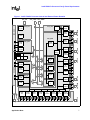
1
Intel® PXA27x Processor Family
Power Requirements
Application Note
Order Number: 280005-002
INFORMATION IN THIS DOCUMENT IS PROVIDED IN CONNECTION WITH INTEL® PRODUCTS. NO LICENSE, EXPRESS OR IMPLIED, BY
ESTOPPEL OR OTHERWISE, TO ANY INTELLECTUAL PROPERTY RIGHTS IS GRANTED BY THIS DOCUMENT. EXCEPT AS PROVIDED IN
INTEL'S TERMS AND CONDITIONS OF SALE FOR SUCH PRODUCTS, INTEL ASSUMES NO LIABILITY WHATSOEVER, AND INTEL DISCLAIMS
ANY EXPRESS OR IMPLIED WARRANTY, RELATING TO SALE AND/OR USE OF INTEL PRODUCTS INCLUDING LIABILITY OR WARRANTIES
RELATING TO FITNESS FOR A PARTICULAR PURPOSE, MERCHANTABILITY, OR INFRINGEMENT OF ANY PATENT, COPYRIGHT OR OTHER
INTELLECTUAL PROPERTY RIGHT. Intel products are not intended for use in medical, life saving, or life sustaining applications.
Intel may make changes to specifications and product descriptions at any time, without notice.
Designers must not rely on the absence or characteristics of any features or instructions marked “reserved” or “undefined.” Intel reserves these for
future definition and shall have no responsibility whatsoever for conflicts or incompatibilities arising from future changes to them.
The Intel® PXA27x processor may contain design defects or errors known as errata which may cause the product to deviate from published
specifications. Current characterized errata are available on request.
This document and the software described in it are furnished under license and may only be used or copied in accordance with the terms of the
license. The information in this document is furnished for informational use only, is subject to change without notice, and should not be construed as a
commitment by Intel Corporation. Intel Corporation assumes no responsibility or liability for any errors or inaccuracies that may appear in this
document or any software that may be provided in association with this document. Except as permitted by such license, no part of this document may
be reproduced, stored in a retrieval system, or transmitted in any form or by any means without the express written consent of Intel Corporation.
Contact your local Intel sales office or your distributor to obtain the latest specifications and before placing your product order.
Copies of documents which have an ordering number and are referenced in this document, or other Intel literature may be obtained by calling
1-800-548-4725 or by visiting Intel's website at http://www.intel.com.
Copyright © Intel Corporation, 2004
AlertVIEW, i960, AnyPoint, AppChoice, BoardWatch, BunnyPeople, CablePort, Celeron, Chips, Commerce Cart, CT Connect, CT Media, Dialogic,
DM3, EtherExpress, ETOX, FlashFile, GatherRound, i386, i486, iCat, iCOMP, Insight960, InstantIP, Intel, Intel logo, Intel386, Intel486, Intel740,
IntelDX2, IntelDX4, IntelSX2, Intel ChatPad, Intel Create&Share, Intel Dot.Station, Intel GigaBlade, Intel InBusiness, Intel Inside, Intel Inside logo, Intel
NetBurst, Intel NetStructure, Intel Play, Intel Play logo, Intel Pocket Concert, Intel SingleDriver, Intel SpeedStep, Intel StrataFlash, Intel TeamStation,
Intel WebOutfitter, Intel Xeon, Intel XScale, Itanium, JobAnalyst, LANDesk, LanRover, MCS, MMX, MMX logo, NetPort, NetportExpress, Optimizer
logo, OverDrive, Paragon, PC Dads, PC Parents, Pentium, Pentium II Xeon, Pentium III Xeon, Performance at Your Command, ProShare,
RemoteExpress, Screamline, Shiva, SmartDie, Solutions960, Sound Mark, StorageExpress, The Computer Inside, The Journey Inside, This Way In,
TokenExpress, Trillium, Vivonic, and VTune are trademarks or registered trademarks of Intel Corporation or its subsidiaries in the United States and
other countries.
*Other names and brands may be claimed as the property of others.
ii
Application Note
Intel® PXA27x Processor Family Power Requirements
Contents
Contents
1.0
Introduction....................................................................................................................................5
1.1
2.0
Naming Conventions ............................................................................................................ 5
Intel® PXA27x Processor Power Supply Domains..................................................................... 5
2.1
2.2
Power Domains and System Voltage/Current Requirements ...............................................8
2.1.1 Intel® PXA27x Processor Power Supplies .............................................................. 8
2.1.2 Power Supply Configuration in a Minimal System .................................................10
2.1.3 Intel® PXA27x Processor Supply Current for Each Power Domain ......................11
2.1.4 Intel® PXA27x Processor VCC_CORE Supply Current ........................................ 12
2.1.5 Default Reset Values ............................................................................................. 13
Batteries.............................................................................................................................. 14
2.2.1 Main Battery........................................................................................................... 14
2.2.2 Backup Battery ......................................................................................................14
2.2.3 Battery Chargers and Main Power......................................................................... 15
3.0
Intel® PXA27x Processor Low Power Operating Modes ......................................................... 17
4.0
Power Controller Interface Signals............................................................................................18
4.1
4.2
4.3
4.4
4.5
4.6
4.7
4.8
5.0
Power Mode Sequencing ............................................................................................................22
5.1
5.2
6.0
Power-On............................................................................................................................ 22
5.1.1 Cold-Start Power-On and Hardware Reset............................................................ 22
5.1.2 Initial Power Up and Deep Sleep Exit Sequence................................................... 23
5.1.3 Hardware Reset Behavior...................................................................................... 24
Sleep and Deep Sleep........................................................................................................27
5.2.1 Sleep Entry and Exit .............................................................................................. 27
5.2.2 Deep Sleep Entry and Exit.....................................................................................28
Dynamic Voltage Management (DVM) ....................................................................................... 29
6.1
6.2
6.3
6.4
7.0
Power Enable (PWR_EN)...................................................................................................19
System Power Enable (SYS_EN) / GPIO<2>.....................................................................19
Power Manager I2C Clock (PWR_SCL) / GPIO<3>...........................................................19
Power Manager I2C Data (PWR_SDA) / GPIO<4>)...........................................................20
System-Level Considerations for I2C ................................................................................. 20
On, Off, and RESET ........................................................................................................... 20
4.6.1 On and Off Control................................................................................................. 20
4.6.2 User-Initiated Hard Reset Input ............................................................................. 20
4.6.3 nRESET Output from PMIC to the Intel® PXA27x Processor ............................... 21
Universal Subscriber Identity Module (USIM).....................................................................21
Power Manager Capacitor Signals .....................................................................................21
VCC_CORE Regulator and Dynamic Voltage Management .............................................. 29
Intel® PXA27x Processor Voltage Manager....................................................................... 30
Power Manager I2C Interface............................................................................................. 31
DVM Sequencing................................................................................................................31
Fault Management .......................................................................................................................31
7.1
nVDD_FAULT..................................................................................................................... 31
Application Note
iii
Intel® PXA27x Processor Family Power Requirements
Contents
7.2
8.0
nBATT_FAULT ................................................................................................................... 32
Power Management Integrated Circuit Requirements ............................................................. 32
8.1
8.2
8.3
9.0
General PMIC Characteristics ............................................................................................ 32
Features of a PMIC............................................................................................................. 33
Programmable Voltage Control .......................................................................................... 34
8.3.1 DVM Control Register 1......................................................................................... 34
8.3.2 DVM Control Register 2......................................................................................... 34
8.3.3 DVM Control and Status Register 3....................................................................... 35
8.3.4 Other Aspects of an Integrated Power Controller .................................................. 35
Summary ...................................................................................................................................... 35
Figures
1
2
3
4
Intel® PXA27x Processor Internal and External Power Domains ................................................ 7
Typical Battery and External Regulator Configuration................................................................ 16
Overview of Power Management Operating Modes................................................................... 18
Intel® PXA27x Processor Power Manager Sleep Reset State Diagram .................................... 26
Tables
1
2
3
4
5
6
7
8
9
iv
External Power Supply Descriptions ............................................................................................ 6
Intel® PXA27x Processor Voltage Domains................................................................................. 9
Regulators Required to Power the Intel® PXA27x Processor.................................................... 11
Intel® PXA27x Processor Supply Current For Each Power Domain.......................................... 11
Intel® PXA27x Processor VCC_CORE Supply Current ............................................................. 13
Possible Backup Battery Configurations .................................................................................... 14
Intel® PXA27x Processor Operating Modes .............................................................................. 17
Power Controller Interface Signals ............................................................................................. 19
General PMIC Characteristics .................................................................................................... 33
Application Note
Intel® PXA27x Processor Family Power Requirements
1.0
Introduction
The Intel® PXA27x Processor Family (PXA27x processor) is a highly integrated system-on-chip
optimized for handheld battery-powered devices such as PDAs and 2.5G or 3G cell phones. The
PXA27x processor is ideal for products requiring substantial computing and multimedia capability
with very low power consumption.
The PXA27x processor combines a high-performance CPU with a variety of integrated peripheral
functions. The processor has separate power supply domains for the processor core, memory, and
peripherals to enable low-power system design. The PXA27x processor provides several dedicated
control signals as well as an I2C interface to connect to an external power management integrated
circuit.
Other system components, such as SDRAM and flash memory, audio codecs, touchscreen
controllers, and specialized companion chips, have with their own unique power requirements. In
many designs, a highly integrated power controller supplies power for these other components,
particularly those that interface directly to the PXA27x processor. An advanced power controller
can contain circuitry for charging batteries, powering the display panel, and include other analog
functions required by the system.
In any system design, factors such as operating conditions, application workload, environmental
considerations and the sophistication of the device’s power management software all play a role in
determining the amount of power consumed. When designing a system, manufacturers need to take
into account where the device is intended to be used (such as high temperature environments) and
what it is expected to do for an end user (such as play a game, a video or do simple email
transactions).
The Intel® PXA27x Processor Family EMTS provides manufacturers with a typical system power
consumption specification for all frequencies of the processor family. The purpose of this
application note is to provide guidance on how power consumption, in a typical environment can
change, based on different software workloads. In addition, this application note provides further
details on the requirements for providing power to the processor and for interfacing to its power
control signals, including behavioral requirements and typical system design examples under these
workloads.
The power numbers generated utilized Intel development platforms in lab conditions and the
information provided should be used as a guideline only.
1.1
Naming Conventions
In this document, active low items are prefixed with a lowercase “n”.
nRESET
Bits within a signal name are enclosed in angle brackets:
EXTERNAL_ADDRESS<31:0>
nCS<1>
Bits within a register bit field are enclosed in square brackets:
REGISTER_BITFIELD[3:0]
REGISTER_BIT[0]
Application Note
5
Intel® PXA27x Processor Family Power Requirements
The terms run mode and normal mode are used interchangeably, although normal mode comprises
both the run-mode and turbo-mode settings.
2.0
Intel® PXA27x Processor Power Supply Domains
Viewed externally, the main or backup battery powers ten power-supply domains. Additional
supply domains are present internally, but power for these is derived from the external supply
inputs.
All functional units within a power domain connect to the same power supply and are powered up
and down together. The PXA27x processor architecture, with its multiple power-supply domains,
provides flexibility in system configuration (including selection of I/O voltages for different
memory and peripherals) and efficient power management (for instance, flexibility in selecting
which peripherals are powered at the same time). Together, these let system designers make power/
complexity trade-offs and optimize a product for intended markets.
Product designers can also choose to strap certain supplies together (to power several domains
from a common regulator) to reduce complexity, cost, and the number of regulators in the system.
Guidelines showing which supplies can be combined are provided in this document.
A summary of the voltage and tolerance requirements for each external supply input is shown in
Table 1. Figure 1 shows the PXA27x processor internal and external power domains and their
connections.
Table 1.
External Power Supply Descriptions
Power Domain
Enable1
VCC_BATT
None
VCC_IO
Units
Specified Levels
(Volts)
Tolerance
(%)
Sleep-control subsystem, oscillators and
real-time clock
3.0
SYS_EN
Peripheral input/output
3.0, 3.3
VCC_LCD
SYS_EN
LCD input/output
1.8, 2.5, 3.0, 3.3
VCC_MEM
SYS_EN
Memory controller input/output
1.8, 2.5, 3.0, 3.3
VCC_BB
SYS_EN
Baseband interface
1.8, 2.5, 3.0, 3.3
VCC_USIM
SYS_EN
USIM interface
1.8, 3.0
VCC_USB
SYS_EN
Differential USB input/output
3.0, 3.3
±10
VCC_PLL
PWR_EN
Phase-locked loops
1.3
±10
VCC_SRAM
PWR_EN
Internal SRAM units
1.1
VCC_CORE
PWR_EN
CPU and other internal units
variable 0.85 –
± 25
±10 (@ 3.0 V
=10%, -10.3%)
+20,-5 (@ 1.8 V)
otherwise ±10
+20,-5 (@ 1.8 V)
otherwise ±10
+20,-5 (@ 1.8 V)
otherwise ±10
+20,-5 (@ 1.8 V)
otherwise ±10
±10
1.55 1
-5 +10
NOTE: SYS_EN and PWR_EN are PXA27x processor output control signals.
1. PXA27x processors have different maximum frequencies and VCC_CORE voltages. Refer to both of the Intel® PXA27x
Processor Family EMTSs for details.
6
Application Note
Intel® PXA27x Processor Family Power Requirements
Figure 1. Intel® PXA27x Processor Internal and External Power Domains
VCC_SRAM
CPU
MEM
Control
P-PLL
312 M
VCC_PER
VCC_OSC
LCD
Control
SRAM
Control
TXTAL
32.768 k
USB-H
48.000 M
DMA/
Bridge
DC-DC
VCC_R3
L1
SRAM
3
VCC_REG
CPM
32.768 k
ICP
48.000 M
VCC_RTC
VCC_R2
I2 S
prg. frq.
SRAM
2
RTC
32.768 k
MMC
19.500 M
VCC_R1
PWR_I2C
13 M
SRAM
1
VCC_PI
BB
48.000 M
VCC_R0
Timer
13 M
SRAM
0
USIM
48.000 M
JTAG
TCK
VCC_BATT
Application Note
KYBD
32.768 k
VCC_IO
Lin-Reg
SSPs
13 M
PWMs
13 M
I2C
32.842 M
UARTs
14.857 M
AC
(ext clk)
VCC_BB
V-Reg
USB-C
48.000 M
VCC_USIM
PXTAL
13 M
Intr
Control
VCC_MEM
VCC_CPU
VCC_LCD
VCC_PLL
MSHC
19.500 M
VCC_IO
VCC_OSC
C-PLL
prg. frq.
VCC_CORE
VCC_USB
VCC_PLL
7
Intel® PXA27x Processor Family Power Requirements
2.1
Power Domains and System Voltage/Current Requirements
The following sections document the power requirements for the PXA27x processor, but do not
include external support, memory, or other peripheral components.
The power consumption values shown in Table 5 are all worst-case numbers. These numbers give
the worst-case system power-supply requirements and do not reflect typical system power
consumption.
2.1.1
Intel® PXA27x Processor Power Supplies
Viewed externally, the processor can require up to nine independent voltages provided by regulated
supplies. In some cases, multiple voltage domains might be strapped together, reducing the number
of separate regulators to as few as four. Internally, there are more domains, but these are powered
from the externally supplied domains by on-chip regulators. The internal domains are documented
for informational purposes only; the external power controller does not have to consider them in its
design.
Table 2 shows the PXA27x processor voltage domains.
8
Application Note
Intel® PXA27x Processor Family Power Requirements
Table 2.
Intel® PXA27x Processor Voltage Domains (Sheet 1 of 2)
Voltage
VCC_BATT
Description
BATTERY VOLTAGE:
Voltage-limited power from the main battery, or directly from a backup battery, at
nominal 3.0 V (±25%). VCC_BATT must be supplied to start the power manager. When
the main battery is installed, VCC_BATT powers the real-time clock and power
management circuitry during initial power-on, sleep, deep sleep and sleep wake-up, so
it remains powered from the backup battery when the main power source has been
discharged or removed. See Section 2.2, “Batteries” on page 14 for information about
directly connecting VCC_BATT to the backup battery or main battery.
NOTE: The power management integrated circuit (PMIC) output drivers for logic
signals nRESET, nVDD_FAULT, nBATT_FAULT, PWR_SDA, GPIO0 and
GPIO1 must be powered from the VCC_BATT supply. This also applies to all
other digital outputs such as the JTAG signals driving PXA27x processor
inputs on the VCC_REG domain. Any devices that have a digital input driven
by a PXA27x processor digital output powered from the VCC_REG domain
must tolerate output high drive levels between 2.25 V and 3.75 V.
NOTE: VCC_BATT must be driven by a regulator whose output is matched to the
VCC_IO regulator so that VCC_IO and VCC_BATT remain within 200 mV of
each other when the VCC_IO regulator is enabled.
VCC_CORE
CORE VOLTAGE:
Dynamically variable core voltage of 0.85 V to 1.55 V. VCC_CORE also powers internal
peripheral logic blocks such as the memory controller, LCD controller, digital audio, and
serial ports. It does not power the internal SRAM. In a full featured system, this supply
is software controllable as described in Section 6.1, “VCC_CORE Regulator and
Dynamic Voltage Management” on page 29. In a simple system, this supply might be a
fixed voltage chosen to meet the minimum voltage requirement for the highest
frequency at which the PXA27x processor operates. In systems that use standby mode,
there must also be a provision to set VCC_CORE to 1.10 V (±10%) prior to entry into
standby mode. VCC_CORE must be enabled when PWR_EN is asserted and disabled
when PWR_EN is de-asserted.
VCC_PLL
PHASE-LOCK LOOP VOLTAGE:
1.3 V (±10%) for internal PLL circuits, fixed. VCC_PLL must not be connected to
VCC_CORE, even though they both may be at the same voltage: 1.3 V. A separate
low-noise voltage source is recommended to keep the PLL supply clean. This supply
must be enabled when PWR_EN is asserted and disabled when PWR_EN is
de-asserted.
VCC_SRAM
Application Note
Power for the internal SRAM during operation in run or turbo modes. This supply is
fixed at 1.1 V (±10%). If the core supply (VCC_CORE) is also fixed at 1.1V (no dynamic
voltage changes are used and the maximum core clock frequency is not supported),
these two supplies are connected together and powered by a common regulator. In
sleep and deep-sleep modes, VCC_SRAM is powered down and the internal SRAM
banks, under program control, are powered from an internal regulator connected to
VCC_BATT. Doing so retains their contents although no accesses are allowed.
VCC_SRAM must be enabled when PWR_EN is asserted and disabled when
PWR_EN is de-asserted.
9
Intel® PXA27x Processor Family Power Requirements
Table 2.
Intel® PXA27x Processor Voltage Domains (Sheet 2 of 2)
Voltage
VCC_IO
Description
Fixed 3.0 V or 3.3 V (±10%) for standard CMOS I/Os interfacing to external
components, which are also supplied from fixed 3.0 V or 3.3 V. The I/Os for external
components connected to the corresponding signals on the PXA27x processor must be
supplied from the same regulator. Driving VCC_BATT in this manner prevents forwardbiasing of protection diodes and inadvertent charging of the backup battery through
inputs on the PXA27x processor VCC_REG domain. The VCC_IO supply must be the
highest potential in the system (excluding VCC_BATT and VCC_USB) and must be
sequenced on at the same time or before the other supplies enabled by SYS_EN.
VCC_IO are connected to any of the VCC_LCD, VCC_MEM, VCC_BB or VCC_USIM
supplies as long as none of these supplies are driven at a voltage higher than VCC_IO.
VCC_IO must be enabled when SYS_EN is asserted and disabled when SYS_EN is
de-asserted.
NOTE: When the main battery is installed, VCC_BATT must be driven by a regulator
whose output is matched to the VCC_IO regulator so that VCC_IO and
VCC_BATT remain within 200 mV of each other when the VCC_IO regulator is
enabled.
VCC_LCD
Power for output drivers to LCD panel, 1.8 V (+20%, -5%), 2.5 V, 3.0V or 3.3 V (± 10%).
Optionally, these are strapped to one of the existing I/O supplies at 3.3 V, 2.5 V, or
1.8 V if appropriate for the panel used. This supply must be enabled when SYS_EN is
asserted and disabled when SYS_EN is de-asserted.
VCC_MEM
Power for memory/system bus I/O at 1.8 V (+20%, -5%), 2.5 V, 3.0V or 3.3 V (±10%);
fixed, strappable by input signals on the power controller to one of these voltages. The
power controller automatically powers up VCC_MEM to the voltage specified by its
input control signals when this regulator is enabled. Corresponding I/Os of the memory
components or companion chips must be powered from the same regulator. This
supply must be enabled when SYS_EN is asserted and disabled when SYS_EN is
de-asserted.
VCC_BB
Power for I/Os to an external baseband module or device, at 1.8 V (+20%, -5%), 2.5 V,
3.0V,or 3.3 V (±10%). Corresponding I/Os of the baseband device must be powered
from the same regulator. In systems that use PCMCIA or Compact flash and the
baseband interface, VCC_BB must be tied to VCC_MEM because some of the card
interface signals are multiplexed with baseband interface signals. This supply must be
enabled when SYS_EN is asserted and disabled when SYS_EN is de-asserted if any of
these GPIOs are used (as either a GPIO or as an alternate function): GPIO<48>,
GPIO<57:50>, GPIO<85:81>.
VCC_USIM
Power for I/Os to an external Universal Subscriber Identity Module (USIM) card. The
VCC_USIM voltage generated by the PMIC is software configurable at settings of 1.8 V
(+20%, -5%) or 3.0 V (± 10%) or disabled (0 V). The software voltage control is
implemented using I2C commands or the PMIC decodes the PXA27x processor UVS0,
nUVS1, and nUVS2 outputs. Refer to Section 4.7, “Universal Subscriber Identity
Module (USIM)” on page 21 for more information.
VCC_USB
Power for USB at 3.0 V or 3.3V (±10%) for standard differential USB I/Os interfacing to
external components, which are also supplied from fixed 3.0 V or 3.3 V.
NOTE: VCC_USB powers the I/O for the USB interfaces, the USB differential signals
D+. D- is out of compliance with the USB specification if VCC_USB is below
2.8 V.
NOTE: The +5 V VBUS source from USB host controller, which must be available for
bus-powered peripherals, must be supplied from an external source, but it is
not part of the PXA27x processor silicon.
2.1.2
Power Supply Configuration in a Minimal System
For minimal systems, only five (four if VCC_USIM is disabled) regulators are required to power
the PXA27x processor and its input/output interfaces, as shown in Table 3.
10
Application Note
Intel® PXA27x Processor Family Power Requirements
Table 3.
Regulators Required to Power the Intel® PXA27x Processor
Regulator
Description
1
Regulated main battery voltage, nominally 3.0 V (limited to a maximum of 3.75 V) to power
VCC_BATT and charge the optional backup battery also connected to VCC_BATT.
2
VCC_IO, VCC_LCD, VCC_MEM, VCC_BB, VCC_USB connected together (can be powered at
3.0V or 3.3 V (±10%)).
3
VCC_USIM at 1.8V and 3.0 V (±10%)
4
VCC_CORE and VCC_SRAM may be connected together, fixed at 1.1 V. Dynamic voltage
management cannot be used and the maximum core clock frequency is not supported using
this arrangement.
5
VCC_PLL at 1.3 V.
More complex systems might require further separation of supply domains and additional
regulators. Independent PXA27x power domains provide flexibility when supporting peripherals
with different I/O voltages, which makes it possible to reduce overall system power by supporting
1.8 V low-power memory with 3.0 V peripherals.
2.1.3
Modeling Intel PXA27x processor power consumption
This section provides guidelines for the power consumption required for the processor by varying
the software workload. In this analysis, the information is divided into two groups:
- Core (modeled as VCC_CORE) - Section 2.1.3.1
- All other power domains (such as memory controller, LCD, etc.) - Section 2.1.3.2
The core model section contains power consumption data with differing workloads. The model for
the remaining domains shows power consumption data for each domain.
Use the guidelines detailed in Section 2.1.3.1 and Section 2.1.3.2 in conjunction with the Power
Consumption Specifications listed in the Intel® PXA27x Processor Family EMTS.
2.1.3.1
Intel® PXA27x Processor VCC_CORE Supply Current
This section specifies the power consumption expected for VCC_CORE power supply domain
across differing workloads.
Table 4 shows the typical current consumption for the VCC_CORE power domain at room
temperature, at nominal voltage levels but with differing workloads. All data is taken using the
Intel PXA270 Processor Development Kit processor card running low level boot code, no
operating system (unless specified).
— Dhrystones 2.1 - Dhrystones workload. Configured to run 20,000,000 cycles with LCD
disabled.
— MPEG4 Decode - Frame rate unlimited, Intel® IPP Performance Suite v4.0 for the Intel
PXA270 processor for Linux, QVGA LCD with frame buffer in SRAM.
— Power Stress Test Code - Low level code executing a repetitive test case of back to back
64bit MAC instructions in an infinite loop. This stress code is written specifically to
exercise the core power domain to yield data at the higher end of usage. It does not
represent a real application.
Application Note
11
Intel® PXA27x Processor Family Power Requirements
Note:
Table 4.
The figures in Table 4 where taken from a system with no enhanced power management
optimization such as Intel Wireless Speedstep (which allows control over the PXA27x processors
low power modes and dynamically selectable frequency and voltage change capability).
Intel® PXA27x Processor VCC_CORE Supply Current
Frequency
Point @
voltage V
Dhrystones 2.1
Current (mA)
Power
(mW)
MPEG4 Decode
current (mA)
Power
(mW)
Power Stress
Test
Current (mA)
Power
(mW)
624 MHz
1.55 V
658
1019
622
964
1006
1559
503
729
475
689
767
1112
395
533
420
567
594
802
297
371
333
416
436
545
208
239
263
303
295
339
520 Mhz
1.45V
416 MHz
1.35V
312 MHz
1.25V
208 MHz
1.15V
NOTE: Core Frequency shown above/Internal bus = 208MHz/Memclk = 208MHz/SDCLK = 104MHz
Note:
Use these specifications as a guideline for power supply capacity. These typical guidelines will
vary across different platforms and software applications.
2.1.3.2
Supply Current For Each Power Domain
This section provides guidelines for the power consumption that could be seen for each power
supply domain when running a heavily loaded system. Focused workloads were used to exercise
each power supply domain separately. It is important to note that the workloads were designed to
push the power consumption on each domain to a higher than normal level given a typical
environment in order to show what the overall power envelope for these domains could look like.
In a real system, each domain will see varying amounts of power consumption based on the type of
workload run. For instance, an MPEG-4 decoder is going to utilize the memory controller much
more than performing simple email transactions would.
Guidance on the power consumption for each domain in order to show Table 5 lists power-supply
current for each PXA27x processor power domain except for VCC_CORE (Table 4 shows data for
VCC_CORE). The environment test conditions are at room temperature and the voltage levels are
specified below.
Note that the I/O domain regulator(s) (VCC_IO, VCC_LCD, VCC_MEM, VCC_BB,
VCC_USIM, VCC_USB) have additional loading from external devices attached to the PXA27x
processor. For example, when flash memory or SDRAM is connected to the system bus. These
loads must be added to those of PXA27x processor I/Os (if they are powered by the same
regulator) when specifying the total load to be provided by a given regulator.
12
Application Note
Intel® PXA27x Processor Family Power Requirements
Table 5.
Intel® PXA27x Processor Supply Current For Each Power Domain
Current (mA) @
voltage V
Power
(mW)
Power manager and real-time clock max. during power-on and
sleep wakeup
10 @ 3.75 V
37.5
Power manager and real-time clock typical during deep sleep
6 µA @ 3.0 V
20 µW
Name
VCC_BATT
VCC_IO
Functional Units
Peripheral input/output
25 @ 3.3 V
82.5
VCC_LCD
LCD input/output
11 @ 3.3 V
33
VCC_MEM
(3.3V)
Memory controller input/output
300 @ 3.3 V
1080
VCC_MEM1
(1.8V)
Memory controller input/output
150 @ 1.80 V1
2971
Baseband interface
9 @ 3.3 V
30
Differential USB interface
25 @ 3.3 V
82.5
VCC_BB
VCC_USB
VCC_USIM
VCC_PLL
VCC_SRAM
USIM interface
0.3 @ 3.0 V
1
Phase-locked loops
40 @ 1.3 V
52
Internal SRAM
50 @ 1.1 V
55
NOTE:
1. This data does not include the Intel® PXA27x Processor Family with Intel StrataFlash® memory power
requirements. Refer to the appropriate top package data sheet for power requirements and include this data when
sizing power regulators that will support the PXA27x processors with Intel StrataFlash® memory
For each I/O domain, maximum current draw and power use is highest at the 3.3 V supply as
shown. For lower voltages (2.5 V, or 1.8 V) maximum current draw and power use is reduced
following the P=CV2F relationship.
Note:
2.1.4
Use these specifications as a guideline for power supply capacity. These typical guidelines will
vary across different platforms and software applications.
Default Reset Values
Of the nine power domains besides VCC_BATT, two (VCC_SRAM and VCC_PLL) are fixed.
Five domains (VCC_MEM, VCC_IO, VCC_LCD, VCC_BB, and VCC_USB) can take one of
several possible values, but once powered up, remain fixed. VCC_CORE and VCC_USIM are
dynamically variable.
On power up, VCC_BATT is the first voltage supplied to the PXA27x processor; limit
VCC_BATT to a maximum of 3.75 V. Other voltages/power domains power up following a
predefined sequence as set by the control signals, PWR_EN and SYS_EN. Refer to the Intel®
PXA27x Processor Family Electrical, Mechanical, and Thermal Specification for a description of
the power-on sequence.
VCC_SRAM must power up and remain at 1.1 V. VCC_PLL must power up to and remain at
1.3 V. VCC_CORE must power up to any user-selected voltage between 0.85 and 1.55V.
VCC_USIM must default to 0 V at power up.
The five supplies that individually take one of several values are: VCC_IO, VCC_LCD,
VCC_MEM, VCC_BB, and VCC_USB. The voltages required for these domains are determined
by other components in the system and the I/O voltages they use. When the system powers up,
Application Note
13
Intel® PXA27x Processor Family Power Requirements
these supplies must come up at the required voltage to operate reliably and to avoid damage to the
external components. VCC_IO must be the highest potential of the system I/O supplies1. VCC_IO
can be connected to any of VCC_LCD, VCC_MEM, VCC_USIM, VCC_USB and VCC_BB, but
none of these supplies can exceed VCC_IO.
The power-up voltage requirement must be communicated by some input strapping mechanism on
the PMIC if a PMIC can provide more than one voltage level for any of these domains. This
ensures that each regulator powers up to its designated voltage without processor intervention.
Software must read this configuration information using an I2C command.
2.2
Batteries
The PXA27x processor supports a variety of system battery configurations with both a main
battery and backup battery, and a main battery alone.
In systems with only a main battery, the main battery must drive VCC_BATT directly or use a
regulator. In systems with a backup battery, the backup battery connects directly to VCC_BATT or
the backup battery can be connected to a power controller, which in turn drives the PXA27x
processor VCC_BATT.
2.2.1
Main Battery
The main battery is a rechargeable single cell (or multiple cells in parallel) using lithium-ion or
lithium-polymer technology. These batteries typically present a voltage as high as 4.2 V when fully
charged, declining to under 3.0 V as they discharge. A main battery capacity of 500 to 1200 mAh is
typical for most applications.
2.2.2
Backup Battery
The backup battery is a lithium or lithium-manganese coin cell with an output voltage of
approximately 3.0 V. The backup battery is a small rechargeable coin cell permanently mounted to
the printed circuit board (PCB) in many handset applications. The PMIC must include a regulator
and associated circuitry for recharging this type of backup battery. The two backup battery
configurations are shown in Table 6.
1.
14
excluding VCC_BATT and VCC_USB
Application Note
Intel® PXA27x Processor Family Power Requirements
Table 6.
Possible Backup Battery Configurations
Backup Battery
Connection
Description
VCC_BATT and PMIC
The backup battery connects to both the VCC_BATT input and PMIC charging
regulator (driven from the main battery or AC adaptor supply). Powering VCC_BATT
from a battery directly eliminates the inefficiency of an external regulator in the
PMIC, maximizing the battery life in sleep and deep sleep. In such a configuration,
ensure that the requirements for limiting current to the backup battery are observed,
regardless of whether it is a rechargeable or non-rechargeable type. Information on
battery current limits is available from the battery manufacturer. Series resistors and
diodes might be needed to limit intentional charging current, to prevent the backup
battery from being drained by a discharged main battery, and to prevent
unintentional backup battery charging by the PXA27x processor. These components
may be internal or external to the PMIC.
PMIC only
There is more flexibility in the number of cells and allowable charging voltage when
the backup battery is connected only to the PMIC and the PMIC drives VCC_BATT.
In this configuration, the PMIC must ensure that requirements for limiting current into
the backup battery are observed, regardless of whether it is a rechargeable or nonrechargeable type.
The system schematic in Figure 2 shows one recommended configuration for connecting the
PXA27x processor directly to the backup battery. In such a configuration, the regulated main
battery powers VCC_BATT through regulator U7, and the backup battery powers VCC_BATT
when the main battery discharges. Regulator U7 also charges the backup battery and its output
voltage must be chosen to ensure that VCC_BATT remains between 2.25 V and 3.75 V when
VCC_IO is disabled and within 200 mV of VCC_IO when VCC_IO is enabled. D1 protects
regulator U7 from back current when the backup battery drives VCC_BATT to a higher potential
than the output of U7. D3 and R2 are chosen to limit intentional charging current to the backup
battery. D2 and R1 prevent the PXA27x processor from driving unintended charging current into
the backup battery if an input signal on the VCC_REG domain is driven above the backup battery
voltage while the processor is powering the VCC_REG domain from VCC_BATT.
Signals from the PMIC to the processor on the VCC_REG domain must be powered from the
VCC_BATT supply voltage when SYS_EN de-asserts in deep-sleep mode. Doing so prevents
forward-biasing the PXA27x processor input protection diodes.
2.2.3
Battery Chargers and Main Power
The PMIC includes as an option a way of charging the main battery when the system is plugged
into an AC power outlet or through the USB port. An external power brick is often used to convert
the main voltage (90 VAC to 240 VAC) to a low DC voltage suitable for powering the regulators
and charging the batteries.
The PMIC must have an input (voltage detect) that can sense when AC power is supplied to the
system to manage main power. An output from the PMIC must make this information available to a
PXA27x processor GPIO at a suitable voltage (normally, 3.3 V CMOS logic levels). For GPIO<0>
or GPIO<1> to generate deep sleep wake-up events, the PMIC must make the input (voltage
detect) information available as an output to one of these GPIO signals.
Application Note
15
Intel® PXA27x Processor Family Power Requirements
Figure 2. Typical Battery and External Regulator Configuration
PXA27x Processor
16
Application Note
Intel® PXA27x Processor Family Power Requirements
3.0
Intel® PXA27x Processor Low Power Operating
Modes
The PXA27x processor provides several low-power operating modes that temporarily suspend or
power down the core or peripherals to reduce power consumption. The external power supplies are
disabled in some modes. Transitions between certain domains require a sequence of events and
handshakes between the PXA27x processor and the external power management integrated circuit
(PMIC) that are detailed in this section.
The PXA27x processor supports six operating modes, shown in Table 7.
Table 7.
Intel® PXA27x Processor Operating Modes
Operating Modes
Normal mode
(Run/Turbo mode)
Description
All external power supplies are enabled and all internal domains are powered. The CPU
core and peripherals are fully functional.
Idle mode
The clocks to the CPU are disabled but context is retained. The peripherals continue
normal operation. All power supplies are enabled. An interrupt assertion causes the
transition back to normal mode.
Deep Idle mode
The core frequency is at 13 MHz (CCCR[CDPIS] is set) and the processor is in idle
mode.
Standby mode
The clocks to the CPU are disabled and the CPU is placed in a low leakage state but
context is retained. All external power supplies are enabled. Each internal SRAM bank
can be independently placed in a low-power mode where the state is retained but no
activity is allowed under program control. The PLLs are disabled and peripheral
operation is suspended. An interrupt assertion causes the transition back to normal
mode.
Sleep mode
All internal power domains except VCC_RTC and VCC_OSC are optionally powered
down. All clock sources except the real-time clock (RTC) and power manager are
disabled, and all external low-voltage power supplies (VCC_CORE, VCC_PLL, and
VCC_SRAM) controlled by PWR_EN are disabled. Recovery is initiated by external
wake-up events or select internal wake-up events. A system reboot is required because
the program counter is invalid.
Deep sleep mode
All internal power domains except VCC_RTC and VCC_OSC are powered down. All
clock sources except the real-time clock (RTC) and power manager are disabled, and the
external low-voltage supplies (VCC_CORE, VCC_PLL, and VCC_SRAM) controlled by
PWR_EN are disabled. The high-voltage power supplies (VCC_IO, VCC_MEM,
VCC_LCD, VCC_BB and VCC_USIM) controlled by SYS_EN are disabled. The active
internal power domains are powered from one of three internal regulators driven from the
backup battery signal, VCC_BATT. Recovery is initiated by external or select internal
wake-up events and requires a system reboot, because the program counter is invalid.
NOTE: Refer to the Intel® PXA27x Processor Family Developers Manual, “Clocks and Power” section for
more information on low power modes
The state diagram in Figure 3 shows the transitions between operating modes and the events and
conditions that cause or enable transitions.
Application Note
17
Intel® PXA27x Processor Family Power Requirements
Figure 3. Overview of Power Management Operating Modes
Reset Mode
any reset
asserted
reset
de-asserted
Normal Mode
Idle
instruction
CPDIS=1
Interrupt
OR (Fault & xIDAE=1)
Idle
instruction
CPDIS=0
Standby
instruction
Interrupt
OR (Fault & xIDAE=1)
Deep Idle Mode
Idle Mode
Fault & xIDAE=0
Sleep
instruction
Wake-up event
OR (Fault & xIDAE=1)
Wake-up event
OR (Fault & xIDAE=1)
Wake-up event
OR (Fault & xIDAE=1)
Standby Mode
Sleep Mode
Fault & xIDAE=0
Fault & xIDAE=0
Fault & xIDAE=0
Deep Sleep
instruction OR
(Fault & xIDAE=0)
Deep Sleep Mode
4.0
Power Controller Interface Signals
The PXA27x processor has an internal power manager unit (PMU) and a set of I/O signals for
communicating with an external power management integrated circuit (PMIC). These signals are
active for initial power up, certain reset events, device on/off events, and transitions between some
operating modes. In addition, two fault signals are required from the PMIC to communicate the
onset of power supply problems to the processor. These signals and their function are described
fully in Section 7.0.
The PXA27x processor communicates to the power controller using the signals defined in Table 8.
18
Application Note
Intel® PXA27x Processor Family Power Requirements
Table 8.
Power Controller Interface Signals
Signal
Definition
Active State
Signal Direction1
PWR_EN
Power enable
high
Output
SYS_EN
System enable
high
Output
PWR_SCL
I2C bus clock
Clock
Output
2
PWR_SDA
I C bus data
—
Bidirectional
nRESET
Forces an unconditional hardware
reset
low
Input
nBATT_FAULT
Indicates main battery removed or
discharged
low
Input
nVDD_FAULT
Indicates one or more supplies are out
of regulation
low
Input
NOTE: 1. Input and output refers to the signal direction from the standpoint of the PXA27x processor
4.1
Power Enable (PWR_EN)
PWR_EN is an active-high output from the PXA27x processor (input to the PMIC) that enables the
external core power supplies (VCC_CORE, VCC_SRAM, and VCC_PLL). De-asserting
PWR_EN informs the external regulator that the processor is going into sleep mode, and that the
low-voltage core power supplies are to be shut down.
The PMIC turns on the core (low-voltage) supplies in response to PWR_EN assertion to resume
normal operation. The power controller must preserve, during sleep or deep sleep, the previous
state of its regulators including the voltage for the core, so that on resumption of core power, the
regulators return to their last known voltage levels.
4.2
System Power Enable (SYS_EN) / GPIO<2>
SYS_EN is an active-high output from the PXA27x processor (input to the PMIC) that enables the
external system power supplies. De-asserting SYS_EN informs the power supply that the processor
is going into deep-sleep mode, and that the high-voltage system power supplies (VCC_IO,
VCC_LCD, VCC_MEM, VCC_USIM, VCC_BB, and VCC_USB) are to be shut down. Assertion
and de-assertion of SYS_EN occurs in the correct sequence with PWR_EN to ensure the correct
sequencing of power supplies when powering on and off the various voltage domains.
To resume normal operation, the PMIC first turns on the system I/O (high-voltage) supplies in
response to SYS_EN assertion and then turns on the core (low-voltage) supplies in response to
PWR_EN assertion. The power controller must return all system I/O voltages to their pre-deep
sleep mode levels.
4.3
Power Manager I2C Clock (PWR_SCL) / GPIO<3>
The PWR_SCL signal is the power manager I2C clock in to the external PMIC. The I2C serial bus
must operate at a minimum 40 kHz and (optionally) be able to operate at a 160 kHz clock rate.
Application Note
19
Intel® PXA27x Processor Family Power Requirements
4.4
Power Manager I2C Data (PWR_SDA) / GPIO<4>)
The PWR_SDA signal is the power manager I2C data signal to the external PMIC. It functions like
an open-drain signal so either component can pull it down to a logic-low level.
4.5
System-Level Considerations for I2C
Both I2C signals have an alternate function on the PXA27x processor as GPIO signals. Following
cold-start power-on or a hard reset, both signals default to the GPIO mode of operation and are
configured as inputs. An internal (nominally 50 KΩ) pull-down resistor on each signal prevents
them from floating during reset or power-on events. To use the I2C capabilities after power-up or
reset, the PXA27x processor must, while under software control, configure these signals as I2C
signals and disconnect the internal pull-down resistor.
These I2C signals behave functionally like open-drain outputs and require an external pull-up
resistor on the system module in the 2 KΩ to 20 KΩ range1. A typical system uses approximately a
5 KΩ resistor connected to 3.3 V.
The I2C signals from the PXA27x processor are pulled low after power-up or reset events. The
PMIC must ignore those signals (logic low is the asserted or ON state for I2C bus) after either type
of event until the PXA27x processor has asserted PWR_EN and SYS_EN, and the system is
operating normally.
The I2C interface does not support the hardware general call, 10-bit addressing, high-speed mode
(Hs-mode, 3.4 Mbits/s), or CBUS compatibility. Although other compatible protocols, such as
SMBus, can be used with the PXA27x processor I2C interface, they have not been tested for
compatibility.
Refer to the I2C Bus Interface Unit section of the Intel® PXA27x Processor Family Developer’s
Manual for more information.
4.6
On, Off, and RESET
4.6.1
On and Off Control
User-initiated ON and OFF events are accomplished using a push button or similar type of system
power switch. The system power switch is a momentary-contact type; making contact shorts the
normally high input to GND.
The switch signal can be connected directly to a PXA27x processor GPIO input or, preferably, to
the PMIC, which debounces the input and forwards the clean signal to a PXA27x processor GPIO.
This process requires two signals on the PMIC; one input and one output. GPIO<0> or GPIO<1>
are recommended for this purpose because they can generate deep-sleep wake-up events.
4.6.2
User-Initiated Hard Reset Input
This signal from a momentary-contact push button switch connects to a power controller input for
user-initiated hard reset. Detection of hard reset forces assertion of the nRESET output from the
power controller IC to the PXA27x processor. The input must be debounced to cause clean
1.
20
See I2C-Bus Specification 2.1, dated January 2000, by Phillips Semiconductors, order #9398 358 10011, pp. 39-42.
Application Note
Intel® PXA27x Processor Family Power Requirements
assertion of nRESET for a minimum of 50 ms. This type of reset would be used only for a severe
and otherwise unrecoverable hardware or software problem, because it completely resets the state
of the processor and may result in lost data. Refer to the Intel® PXA27x Processor Family
Electrical, Mechanical, and Thermal Specification for the hardware reset timing specification.
4.6.3
nRESET Output from PMIC to the Intel® PXA27x Processor
nRESET is an active-low signal from the PMIC to the PXA27x processor that tells the processor to
enter the hardware-reset state. The assertion of nRESET cannot be gated and causes the PXA27x
processor to enter a complete and unconditional reset state. The nRESET signal contains an
internal resistive pull-up that is always active (no pull-up required on the system module or in the
PMIC).
nRESET is a hard reset that can cause the system to lose state or data when asserted. It is asserted
for a cold start power-on event, or if for any reason the user pushes the system reset button. The
power controller must assert nRESET for both events.
nRESET must remain asserted for at least 50 ms when asserted. When not asserted, nRESET is
pulled up internally to VCC_REG. VCC_REG is normally powered from VCC_IO, except when in
deep-sleep mode, where VCC_REG is powered from VCC_BATT.
All PXA27x processor internal registers and processes are held at their defined reset conditions
during hardware reset. While the nRESET signal is asserted, the only activity inside the PXA27x
processor is the stabilization of the 13.000 MHz oscillator and phase-locked loops. The remaining
internal clocks are stopped and the processor is fully static. Additionally, all signals assume their
reset conditions, and the nBATT_FAULT and nVDD_FAULT signals are ignored. The
nRESET_OUT signal from the PXA27x processor is asserted when the nRESET input signal is
asserted.
4.7
Universal Subscriber Identity Module (USIM)
The PXA27x processor provides signals to control an external regulator that powers the USIM card
interface used in many digital cell phones. The VCC_USIM regulator output voltage is set to 1.8 V
or 3.0 V or disabled (0 V) under software control. The software voltage control is implemented
either by using I2C commands or by decoding the PXA27x processor UVS0, nUVS1, and nUVS2
outputs in the PMIC.
The regulator must drive VCC_USIM to ground when UVS0 is driven high. The regulator must
drive VCC_USIM to 1.8 V when nUVS1 is driven low. The regulator must drive VCC_USIM to
3.0 V when nUVS2 is driven low. The PXA27x processor USIM interface asserts only one of these
signals at a time such that they can be used to control the gate of simple FET switches directly.
Note:
4.8
The regulator that generates VCC_USIM must be disabled using SYS_EN or an I2C command
when the PXA27x processor enters deep-sleep mode. During deep sleep, the UVS0, nUVS1, and
nUVS2 outputs are not driven and cannot control the VCC_USIM regulator.
Power Manager Capacitor Signals
This section describes connection of external capacitors to PXA27x processor signals. These
capacitors do not have a direct design impact on a PMIC but are included here for completeness.
Application Note
21
Intel® PXA27x Processor Family Power Requirements
The PXA27x processor has a low-power DC-to-DC converter that is enabled by software while in
sleep or deep-sleep mode. Enabling the low-power DC-to-DC converter further reduces power
consumption by shutting off the high-power regulators on the PMIC, eliminating losses in the
external power supply subsystem. Use of the sleep mode DC-to-DC converter requires three
external capacitors connected to the PXA27x processor PWR_CAP signals.
These capacitors are required for the DC-to-DC converter:
• A 0.1 µF capacitor connected between the PWR_CAP<0> and PWR_CAP<1> signals
• A 0.1 µF capacitor connected between the PWR_CAP<2> and PWR_CAP<3> signals
A 0.1 µF capacitor connected between the PWR_OUT signal and ground is always required. Use
ceramic, unpolarized capacitors with a low equivalent series resistance (ESR). No other
connections are allowed on the PWR_OUT and PWR_CAP<3:0> signals.
Note:
5.0
The PWR_CAP signals must not be shared with the GPIO<5:8> functions under any conditions.
Power Mode Sequencing
The PXA27x processor supply voltages must be powered up in a specific sequence to avoid
damage to the processor. Refer to the Intel® PXA27x Processor Family Electrical, Mechanical,
and Thermal Specification for power-on-reset timing specifications. In general, VCC_BATT must
be the first domain to be powered on, and the last to be powered off. After that, I/O voltages must
be powered on before internal voltages, and powered off after internal voltages are turned off.
I/O voltages are the higher voltages (1.8 V to 3.3 V) that power the I/O cells: VCC_IO,
VCC_LCD, VCC_MEM, VCC_BB, VCC_USB, VCC_USIM. These voltages must power on first
(after VCC_BATT powers up), and must be the last to power off (before VCC_BATT powers off).
Internal voltages are those that power the PXA27x processor core, the PLLs, and internal SRAM:
VCC_CORE, VCC_PLL, and VCC_SRAM. VCC_CORE ranges from 0.85 V to 1.55 V in normal
operation, while VCC_PLL and VCC_SRAM are fixed at 1.3 V and 1.1 V, respectively.
Within the I/O supply group, VCC_IO must be established at or before (but not after) any other
supply (except VCC_USB). Within the internal supply group, there is no specific sequencing
requirement within the internal supply group. The internal supplies can be turned on or off in any
order, or simultaneously. For powering on from a cold start, each domain must not exceed the
maximum (quickest) ramp rate specification and the power-on timing requirements should be
strictly observed. Refer to the Intel® PXA27x Processor Family EMTS for details.
5.1
Power-On
5.1.1
Cold-Start Power-On and Hardware Reset
Power-on reset occurs when power is first supplied to the backup battery signal VCC_BATT,
following a powered-off condition. All PXA27x processor internal units are reset to a known state
exactly like hardware reset. Power-on reset is a complete and total reset that occurs at initial poweron only.
22
Application Note
Intel® PXA27x Processor Family Power Requirements
5.1.2
Initial Power Up and Deep Sleep Exit Sequence
As shown in Figure 2, the external power management integrated circuit (PMIC) supplies both
high-voltage (I/O) and low-voltage (internal) power to the PXA27x processor. The external voltage
regulator also sources nBATT_FAULT and nVDD_FAULT signals to the PXA27x processor.
There are two power control signals:
• SYS_EN controls the high-voltage (I/O) supplies:
— VCC_IO
— VCC_LCD
— VCC_MEM
— VCC_BB
— VCC_USB
— VCC_USIM
• PWR_EN controls low-voltage (internal) supplies:
— VCC_CORE
— VCC_PLL
— VCC_SRAM
Typically, during system assembly, the fully-charged backup battery is soldered permanently into
the system. To prevent draining the backup battery prematurely, Intel recommends installing the
main battery at least temporarily at this time to prevent draining the backup battery prematurely.
With the backup battery in place, the PXA27x processor begins the initial cold-start, power-up
sequence, enabling its power manager unit and one of the oscillators. Refer to the Intel® PXA27x
Processor Family Electrical, Mechanical, and Thermal Specification for power-on-reset timing
specifications.
The PXA27x processor waits for the assertion of nBATT_FAULT from the PMIC. The PXA27x
processor internal power manager unit (PMU) also powers up its own section of low-power
circuitry with the installation of the backup battery. Doing so allows the PMU to monitor voltages
as they come up and generate the nBATT_FAULT and nVDD_FAULT signals. Because the main
battery is not installed and only VCC_BATT is supplying power to the PXA27x processor, the
PMIC initially must assert both nBATT_FAULT and nVDD_FAULT. (Note that the PMIC outputs
must be powered from the VCC_BATT supply at this time.) The PMIC must not de-assert
nBATT_FAULT until the main battery is inserted and charged.
Note:
When the backup battery is installed but the main battery is not installed, the PXA27x processor
draws approximately 1 mA from the backup battery on VCC_BATT. To preserve the backup
battery life, Intel recommends the temporary installation of a a main battery long enough to
complete an initial boot sequence and run software to configure the PXA27x processor to enter
deep-sleep mode using the internal DC-to-DC converter.
The GPIO pins on the PXA27x processor initially default to inputs, so they cannot be used for
power regulator control at initial power up, or for exiting deep-sleep mode unless they have been
programmed to respond to an edge or level change.
Application Note
23
Intel® PXA27x Processor Family Power Requirements
Note:
The nRESET signal must be asserted earlier in the reset sequence for the processor. Refer to the
Intel® PXA27x Processor Family Electrical, Mechanical, and Thermal Specification for power-on
reset timing specifications.
The sequence for initial (start-of-life) power-on reset is as follows:
1. VCC_BATT power is applied to the processor and reaches a stable voltage of at least 2.25 V
(initiating the power-on reset event) with nRESET asserted from PMIC to the processor.
2. The PMIC must assert nBATT_FAULT because the main battery is not installed.
3. The PMIC de-asserts nRESET after a minimum of 50 ms.
4. The PXA27x processor enables its internal PMU, which waits for the de-assertion of
nBATT_FAULT to indicate main battery installation.
5. The fully charged main battery is installed and the PMIC de-asserts nBATT_FAULT.
6. The PXA27x processor asserts SYS_EN to enable the system high-voltage I/O power
supplies. The PXA27x processor starts its SYS_DEL countdown timer set to the default
125 ms period.
7. The PMIC enables the regulators driving VCC_IO, and then VCC_LCD, VCC_MEM,
VCC_USIM, VCC_BB, and VCC_USB. The latter regulators power on and achieve
regulation in any order.
8. After the 125 ms SYS_DEL timer expires, the PXA27x processor asserts PWR_EN to enable
the PXA27x processor low-voltage power supplies. Refer to the Intel® PXA27x Processor
Family Electrical, Mechanical, and Thermal Specification for Power-On reset timing
specifications. The PXA27x processor starts its PWR_DEL countdown timer set to the default
125 ms period.
9. The PMIC enables the regulators driving VCC_CORE, VCC_PLL, and VCC_SRAM. These
regulators power on and achieve regulation in any order.
10. The PMIC de-asserts nVDD_FAULT when all supplies are stable and within regulation
specifications.
11. After the 125 ms PWR_DEL timer expires, the PXA27x processor samples the
nVDD_FAULT input. If nVDD_FAULT is asserted, the PXA27x processor returns to sleep or
deep-sleep mode; otherwise, the sequence continues.
12. The PXA27x processor continues its power up initialization by enabling the processor
(13.000 MHz) oscillator and internal PLLs and switching the I/O supply power for the internal
domains from VCC_BATT to VCC_IO.
13. The PXA27x processor de-asserts the nRESET_OUT signal and begins the execution of code
from the reset vector.
Refer to the Intel® PXA27x Processor Family Electrical, Mechanical, and Thermal Specification
for power-on reset timing specifications.
5.1.3
Hardware Reset Behavior
Hardware reset initiates when the PMIC asserts the nRESET signal low. On assertion of nRESET,
the PXA27x processor enters hardware reset state and asserts nRESET_OUT. The PMIC must hold
nRESET low long enough to allow internal stabilization and propagation of the reset state, which is
a minimum of 50 ms.
The sequence for hardware reset is as follows:
24
Application Note
Intel® PXA27x Processor Family Power Requirements
1. The PMIC asserts nRESET.
2. The PXA27x processor asserts the nRESET_OUT1 signal. The time between nRESET
assertion and nRESET_OUT assertion depends on whether this event the PXA27x processor
was previously running or whether this is an initial power up event.
3. The PMIC de-asserts nRESET after a minimum of 50 ms from nRESET assertion.
4. The internal processor PMU waits for the 13.000 MHz oscillator and internal PLLs to
stabilize, if needed.
5. The PXA27x processor de-asserts the nRESET_OUT signal.
The timing for hardware reset is shown in the Intel® PXA27x Processor Family Electrical,
Mechanical, and Thermal Specification. The PXA27x processor power manager sleep reset state is
shown in Figure 4. The timing between nRESET assertion and nRESET_OUT assertion is shown
in the Intel® PXA27x Processor Family Electrical, Mechanical, and Thermal Specification data
sheet.
Application Note
25
Intel® PXA27x Processor Family Power Requirements
Note:
1) nRESET_OUT assertion is software programmable during processor resets. Refer to the Intel®
PXA27x Processor Family Developer’s Manual.
Figure 4. Intel® PXA27x Processor Power Manager Sleep Reset State Diagram
Enable
PLL
pll_ok = 1
Normal
Run
Mode
(Software initiated
deep sleep) OR
nVDD_FAULT = 0
Initial
Power
Up
nBATT_FAULT = 0
clk_32k_ok = 1
Deep
Sleep
nBATT_FAULT = 1
Deep
nBATT_FAULT = 0
Sleep
wakeup = 1 &
nBATT_FAULT = 1
wakeup = 1 &
nBATT_FAULT = 0
wakeup = 1 &
nBATT_FAULT = 1
SYS_EN = 1
Wakeup
while
Batt Fault
de-asserted
Batt fault
wakeup = 1 &
nBATT_FAULT = 0
Wakeup
while
nBATT_FAULT = 1
Batt Fault
asserted
Count
Down
SYS_DEL
nBATT_FAULT = 0
(count_done = 1 & nBATT_FAULT = 1) OR
(all_vcc_hi = 1 & PSSD = 1 & nBATT_FAULT = 1)
PWR_EN = 1
All external IO pads use
VCC_IO or corresponding power
supply. Power manager continues
to use VCC_BATT
Assert
pwr_
enable
Count
Down
PWR_DEL
(nBATT_FAULT = 1 & nVDD_FAULT = 1) &
(count_done = 1 OR all_vcc_low = 1 & PSSD = 1)
nBATT_FAULT = 0
nBATT_FAULT = 0
(nVDD_FAULT = 0) & (count_done = 1)
= power manager powered by VCC_CORE
= power manager powered by VCC_BATT
26
Application Note
Intel® PXA27x Processor Family Power Requirements
5.2
Sleep and Deep Sleep
The sleep and deep-sleep modes reduce power consumption by powering down most units in the
PXA27x processor. However, the real-time clock, timekeeping oscillator (32.768 kHz), and PMU
circuits remain active. The processor oscillator (13.000 MHz), power manager I2C, and JTAG units
may also be active. One, two, or four banks of internal SRAM can (optionally) remain powered in
sleep mode to retain data, at the expense of approximately 100 µW per bank.
In sleep and deep-sleep modes, the PXA27x processor power supplies VCC_CORE, VCC_SRAM,
and VCC_PLL can be disabled to achieve greater system power savings. In deep- sleep mode, the
system power supplies VCC_IO, VCC_LCD, VCC_USIM, VCC_BB, VCC_USB, and
VCC_MEM can also be powered down for additional power savings. The PXA27x processor then
uses VCC_BATT to power an internal DC-to-DC converter, optimized for high efficiency at low
power, to create the internal supplies.
The penalty for removing power from VCC_CORE and VCC_SRAM is that the processor
execution state is lost. Once the processor activity has stopped, recovery from sleep and deep-sleep
modes must be through an external wakeup event or a real-time clock timer event that initiates a
sleep reset sequence to boot the PXA27x processor again.
Retaining SDRAM contents while in sleep and deep-sleep modes requires an additional, efficient
low-current supply powered from either the main or backup battery. Pull down the PXA27x
processor SDCKE signal to retain SDRAM contents while in sleep and deep sleep.
Before entering the sleep or deep-sleep modes, software must program the appropriate registers
within the PXA27x processor to:
• Set up delay timers
• Shut off internal functional blocks
• Specify the wakeup sources for exiting sleep or deep sleep
Software initiates entry into sleep or deep sleep (for example, the user presses the OFF button and
closes the unit cover), or by a hardware event such as assertion of the nVDD_FAULT or
nBATT_FAULT signals from the PMIC. See Section 7.0 for fault conditions and interaction
between the PXA27x processor and the PMIC during those events.
5.2.1
Sleep Entry and Exit
Prior to entering sleep mode, the PXA27x processor prepares the PMIC by specifying which
additional system regulators, if any, are to be disabled or shut down when the PMIC is commanded
to go into sleep mode. The set of regulators to be turned off can be fixed in PMIC hardware, or it
might be programmable. If programmable, a register in the PMIC is loaded via I2C to specify
which regulators turn off. For optimal power savings during sleep, enable and disable the
VCC_CORE, VCC_PLL, and VCC_SRAM regulators using PWR_EN, but other regulators in the
system may or may not require enabling/disabling, depending upon system design. For example, if
a memory device or peripheral must retain its contents during sleep under certain conditions, it may
require another regulator that is software controllable.
The PXA27x processor places DRAM memory into self-refresh mode. Note that in self-refresh
mode, the DRAM must still be powered, but power decreases substantially. Alternatively, if
DRAM contents do not need to be preserved, the processor places the DRAMs into deep-powerdown mode. Doing so reduces DRAM power to microamps, even though voltage from the PMIC is
still maintained on the DRAM power signals.
Application Note
27
Intel® PXA27x Processor Family Power Requirements
The processor commands entry into sleep mode by de-asserting PWR_EN to the PMIC once the
PMIC and system are prepared. The PMIC responds by turning off the specified set of supplies
along with VCC_CORE, VCC_PLL, and VCC_SRAM. For entry into sleep mode, there is no
requirement for how long these supplies require to shut down after de-assertion of PWR_EN.
(However, for entry into deep-sleep mode, these supplies must shut down before the de-assertion of
SYS_EN to ensure that supply sequencing requirements are met.)
A wakeup event must occur to exit sleep mode. For example, the wakeup event can be a transition
on one of the wakeup-capable GPIOs that has been programmed to respond to a level change, or it
can be an interrupt from a timer in the real-time clock unit. In response, the PXA27x processor
asserts PWR_EN to the PMIC and starts its PWR_DEL timer. The PMIC turns on all of its lowvoltage supplies (VCC_CORE, VCC_SRAM, and VCC_PLL) and when all supplies are stable and
within regulation, the PMIC de-asserts nVDD_FAULT. The PXA27x processor returns the system
to sleep mode if nVDD_FAULT is not de-asserted before the PWR_DEL timer expires. Otherwise
the PXA27x processor completes the sleep-reset boot sequence. See the Intel® PXA27x Processor
Family Electrical, Mechanical, and Thermal Specification data sheet for entry and exit sleep-mode
timings.
Note:
5.2.2
Upon exiting from sleep mode, the processor returns to the last clock frequency prior to sleep mode
entry. Likewise, the PMIC must also be able to return to the previous voltage level prior to entering
sleep mode. It is necessary for the PMIC to accommodate the appropriate voltage level upon
exiting. All wake-up events are ignored until nBATT_FAULT is de-asserted if the nBATT_FAULT
signal asserts in sleep or deep sleep.
Deep Sleep Entry and Exit
The PXA27x processor prepares the PMIC for deep sleep prior to entering deep sleep by
specifying which additional system regulators are to be disabled or shut down when the PXA27x
processor commands deep-sleep entry. The PXA27x processor controls deep-sleep entry by deassertion of the SYS_EN signal. The set of regulators to be turned off can be fixed in PMIC
hardware or it can be programmable. If programmable, a register in the PMIC is loaded via I2C to
specify which regulators turn off. The regulators for VCC_IO, VCC_LCD, VCC_MEM,
VCC_BB, VCC_USB, and VCC_USIM are enabled and disabled using SYS_EN, but other
regulators in the system may or may not need to be enabled/disabled, depending upon system
design.
The PXA27x processor places DRAM memory into self-refresh mode before entering deep sleep.
In self-refresh mode, the DRAM must still be powered, but power decreases substantially.
Alternatively, if DRAM contents do not need to be preserved, the PXA27x processor can place the
DRAMs into deep-power-down mode. Doing so reduces DRAM power to microamps, even though
voltage from the PMIC is still maintained on the DRAM power signals.
Note:
The PXA271 and PXA272 processors contain stacked memory which is supplied power via the
VCC_MEM power domain.
The PXA27x processor commands entry into deep-sleep mode by de-asserting PWR_EN once the
PMIC and system are prepared. The PMIC responds by turning off the set of low-voltage power
supplies designated either by the prior register setting, or fixed in PMIC hardware. After a delay to
allow the low-voltage supplies to shut down, the PXA27x processor de-asserts SYS_EN to the
PMIC, and the PMIC responds by turning off the necessary combination of high-voltage supplies.
Note that all power-supply sequencing requirements must be observed: low-voltage supplies must
power down before any high-voltage supplies power down. See the Intel® PXA27x Processor
Family Electrical, Mechanical, and Thermal Specification data sheet for entry and exit deep-sleep
mode timings.
28
Application Note
Intel® PXA27x Processor Family Power Requirements
Note:
If the PMIC does not disable VCC_CORE, VCC_PLL, or VCC_SRAM when PWR_EN is deasserted, the PMIC must not disable any of the regulators controlled by SYS_EN when SYS_EN is
de-asserted to ensure that supply sequencing requirements are satisfied.
A wakeup event must occur to exit deep sleep. The wakeup event can include the following:
• A transition on one of the deep sleep wakeup-capable GPIOs that has been programmed to
respond to an edge or level change
• An interrupt from a timer in the real-time clock unit
Upon exiting from deep-sleep mode, the processor returns to the last clock frequency prior to deepsleep mode entry. Likewise, the PMIC must also be able to return to the previous voltage level
prior to entering deep-sleep mode. The PMIC must accommodate the appropriate voltage level
upon exiting.
The PXA27x processor asserts SYS_EN to the PMIC and starts its SYS_DEL timer. The PMIC
turns on its high-voltage supplies (VCC_IO, VCC_LCD, VCC_USIM, VCC_BB, VCC_USB, and
VCC_MEM). After waiting the period set by SYS_DEL, the processor asserts PWR_EN to the
PMIC and starts its PWR_DEL countdown timer. The PMIC turns on the low-voltage supplies
(VCC_CORE, VCC_SRAM, and VCC_PLL) and de-asserts nVDD_FAULT when all supplies are
stable and within regulation. If nVDD_FAULT is not de-asserted before the PWR_DEL timer
expires, the PXA27x processor returns the system to deep-sleep mode; otherwise, the PXA27x
processor completes the sleep-reset boot sequence.
Note:
If the nBATT_FAULT signal asserts in sleep or deep sleep, all wake-up events are ignored until
nBATT_FAULT is de-asserted.
If the deep-sleep configuration is set and PSLR[PSSD] (sleep mode shorten wakeup delay disable
bit) is set, the PXA27x processor shortens the wakeup sequence by asserting PWR_EN as soon as
the PXA27x processor PMU detects all the corresponding power supplies have powered up, as
shown in Figure 4. Refer to the Intel® PXA27x Processor Family EMTS manual for deep-sleep
entry and exit timing specifications.
6.0
Dynamic Voltage Management (DVM)
The PXA27x processor has a number of features that enable the dynamic management of power
consumption, which is based on the computing power required at any particular time. These
features enable the processor to modify the core frequency voltage of the processor during
operation, dynamically matching the computing performance to the current computing workload.
A system combining the PXA27x processor, a power management integrated circuit (PMIC), and
supporting DVM software can run a wide range of applications using only a fraction of the battery
power that would be required running at the fixed frequency and voltage needed for the peak
computing workload.
6.1
VCC_CORE Regulator and Dynamic Voltage Management
The PMIC must have these minimum features for its VCC_CORE regulator to support dynamic
voltage and frequency management:
• High-efficiency I2C programmable buck1 converter output providing VCC_CORE in the
voltage range 0.85-1.55 V (-5%/10%) with a default/reset output in the same range.
Application Note
29
Intel® PXA27x Processor Family Power Requirements
• I2C programmable output voltage ramp rate with a default/reset ramp rate of 10mV/µs. Refer
to the Intel® PXA27x Processor Family EMTS for ramp rate specifications
The VCC_CORE regulator must support a minimum set of these six output voltages: 0.85, 0.95,
1.1, 1.2, 1.3, 1.4 and 1.55 V. It is preferable to provide more voltage steps by dividing the range
between 0.85 V and 1.55 V using a step size of 10 to 50 mV. The accuracy of each voltage set point
must be at least ± 1 voltage step. When using more than the minimum set of five steps it is not
necessary to support these five exact step values.
The VCC_CORE regulator must also support programming the voltage ramp rate over a onedecade range of the nominal default value (10mV per µs). Ramping is accomplished via a smooth
analog ramp driven by an internal ramp generator, or through a series of microsteps of 10-25 mV
per microstep, which are performed sequentially after a small delay to make up the requested
change in voltage. Faster ramp rates can, in practice, be limited by the capabilities of the regulator
and by the amount of bulk capacitance on the VCC_CORE supply.
Controlling the core voltage is accomplished by loading registers in the PMIC via the I2C serial
bus. The bus transfers data one byte at a time to the PMIC. Register loads are 8 bits wide, although
not all bits need be used by accompanying circuitry. If voltage ramps are comprised of a series of
microsteps, the step rate can be programmed as increments of the PMIC internal oscillator used by
its voltage converters. Many switching regulators use oscillators in the 500 kHz to 1 MHz range.
Section 8.0 contains more information on the recommended PMIC register set and bit fields.
The worst-case load, or maximum di/dt (from the slowest run mode setting to the fastest turbo
mode setting) expected is 200 mA per 10 ns.
Note:
6.2
It may be advantageous to allow scaling of the VCC_CORE domain above 1.55V for debug
purposes, which would require the PMIC and associated power circuitry being able to drive
VCC_CORE up to 2.0V.
Intel® PXA27x Processor Voltage Manager
The PXA27x processor power manager unit (PMU) includes an internal voltage manager unit with
a dedicated I2C interface and a command sequencer. The I2C interface provides the PXA27x
processor with dynamic and static voltage control capability, using an I2C module for
communicating with the external PMIC. The voltage manager provides these features:
•
•
•
•
Static (Halted) or dynamic (operational) voltage change
Up to 32 I2C commands automatically sent to I2C
Single and multi-byte I2C command support
The PXA27x processor I2C commands are user defined to match the format defined by the
PMIC.
• Programmable delay between commands
1.
30
A step-down, or voltage dropping converter
Application Note
Intel® PXA27x Processor Family Power Requirements
6.3
Power Manager I2C Interface
The PXA27x processor communicates with the PMIC using the I2C serial bus. The flexible I2C
controller in the processor can pre-load a buffer with a series of commands, or multi-byte
commands of any size, up to a total of 32 bytes of command address and data. The I2C controller
can be programmed to send a series of commands with programmable intervals between groups of
commands to accommodate a variety of different power controllers and regulators.
Refer to the Intel® PXA27x Processor Family EMTS for voltage change timing specifications.
The I2C interface runs in either standard mode at 40 kHz or fast mode at 160 kHz using standard 7bit addressing. The hardware general call and 10-bit extended addressing are not supported.
6.4
DVM Sequencing
The PMIC contains registers that enable, at a minimum, these functions:
• Programming a voltage change from the current voltage to a new voltage
• Programming a ramp rate at which the voltage change occurs
• A GO bit, which once set, triggers the requested voltage change
7.0
Fault Management
The PXA27x processor provides two digital status inputs (nBATT_FAULT and nVDD_FAULT)
driven by the external PMIC that indicate status of the main battery and the power-supply
regulators. These signals permit a combination of hardware and software management of power
fault conditions.
Both signals are asserted low to the PXA27x processor inputs. They can be used to place the
processor into sleep or deep sleep power-down modes to reduce power quickly and to preserve as
much system state or context as possible. Entry into sleep or deep sleep can be initiated directly by
the PXA27x processor PMU hardware upon assertion of nBATT_FAULT and nVDD_FAULT, or
these events can trigger a software exception handler that saves the system state and issues the
command to enter sleep or deep sleep. The PXA27x processor power manager PMCR[BIDAE] and
PMCR[VIDAE]1 control bits select between hardware or software handling of these respective
fault events.
7.1
nVDD_FAULT
nVDD_FAULT signals the PXA27x processor that one or more of its currently enabled supplies
are below the minimum regulation limit (supplies that are not enabled do not cause nVDD_FAULT
assertion). Functionally, nVDD_FAULT signals the processor when it is safe to exit sleep or when
it must enter sleep (using the mechanism selected by the PMCR[VIDAE] setting). nVDD_FAULT
is ignored after a wakeup event until the SYS_DEL and PWR_DEL timers expires. The PXA27x
processor also has a configuration bit2 that allows nVDD_FAULT to be ignored in sleep mode.
1.
2.
See the Intel® PXA27x Processor Family Developer’s Manual
The PSLR[IVF] bit; see the Intel® PXA27x Processor Family Developer’s Manual
Application Note
31
Intel® PXA27x Processor Family Power Requirements
System designers can include a software-controlled threshold level detection for nVDD_FAULT to
allow an optional SDRAM keep-alive capability.
7.2
nBATT_FAULT
nBATT_FAULT indicates that the main battery is low or has been removed from the device, giving
the PXA27x processor an indication that power will shortly cease. Until that time, the processor
can operate for a limited period from a lithium/lithium manganese coin-cell backup battery, or from
a super cap that can only supply the processor for a few cycles of full-run power.
In the event of nBATT_FAULT assertion, the PXA27x processor enters an emergency form of
sleep, where the only handshaking is with external SDRAM memory (putting it into self-refresh
mode) to ensure that memory contents are preserved if possible (obviously, the refresh current can
eventually deplete the super cap or backup battery, but not as quickly as the PXA27x processor in
run mode). Supporting these features must be understood at both the board-level design and by the
PMIC.
Note:
The PXA27x processor does not recognize a wakeup event while nBATT_FAULT is asserted.
If the system is powered from an AC main source (90 VAC to 240 VAC or equivalent) while
nBATT_FAULT is asserted, that fact may be used to gate off nBATT_FAULT and its normal
effects on the system. Recognition of this condition can be built into the PMIC, and a signal
indicating an AC power source is active is provided from the PMIC to the PXA27x processor
GPIO<0> or GPIO<1> signals.
8.0
Power Management Integrated Circuit
Requirements
This section provides guidelines for designing a power management integrated circuit (PMIC) for
the PXA27x processor.
8.1
General PMIC Characteristics
Table 9 shows the overall characteristics for a PXA27x processor PMIC.
32
Application Note
Intel® PXA27x Processor Family Power Requirements
Table 9.
General PMIC Characteristics
Characteristic
Highly Integrated,
Multi-Function
8.2
Description
Incorporating buck, boost, buck-boost, and LDO regulators for the PXA27x processor
and surrounding system elements, with dynamic voltage management (DVM) logic for
the core supply. It includes power-up, power-down, and sleep mode power sequencing,
and generates correct nRESET, nBATT_FAULT, and nVDD_FAULT outputs for the
system. Ideally, it also incorporates battery charger circuits and an output to notify the
system when AC power input is present; touchscreen and audio CODECs would be a
plus, if they can meet industry-standard noise and distortion requirements when
combined on the same silicon.
Low-Cost
High integration provides a packaged device that must be lower cost than the
alternative comprised of discrete power supply devices.
High Efficiency
Converters operate in the 85-95% efficiency range under all load conditions, and with
very low quiescent current and shutdown currents (off or sleep mode).
I2C Interface
Must be standard I2C interface operating at either 40 kHz standard mode or 160 kHz
fast-mode clock rate.
Stable and Accurate
Meets ± 3% accuracy or better at the PMIC output signals over input variation, load
variation, and temperature for all regulators and converter outputs. Switching
regulators must minimize noise propagated into regulator outputs.
Reliable
Current and thermal limiting on all regulators.
Features of a PMIC
The basic features of a PMIC for use with the PXA27x processor include:
•
•
•
•
•
•
•
•
Multiple channels of regulated power output
Dynamic voltage management (DVM) capability for the PXA27x processor core supply
Debounced push button ON/OFF and user-reset inputs
AC adapter detect capability
Power-on / user reset output to the PXA27x processor nRESET input
nBATT_FAULT signal, signifying main battery removed
nVDD_FAULT signal, indicating any power regulator out of spec
Automatic switch over from main battery to backup battery when main battery is discharged or
removed
• Responds to the PXA27x processor mode change requests by switching regulators on or off
• Control and Status registers accessible through I2C interface
• Provides USIM power FET control to supply 3.0 V or 1.8 V to USIM card
The features of a PMIC for battery charging also include:
•
•
•
•
Application Note
Charging capability for lithium-ion or lithium-polymer main battery
Support for either rechargeable or non-rechargeable backup battery
Digital output battery level monitor (“fuel gauge”) for main and backup batteries (optional)
Battery charging current and temperature monitoring, for fast charging of main battery
(optional)
33
Intel® PXA27x Processor Family Power Requirements
• USB on-the-go charge pump which generates +5.0 V (optional)
The following analog/mixed-signal features are required in many handheld or battery-powered
systems, and it is a good idea to provide them in a highly integrated PMIC:
•
•
•
•
•
•
•
•
•
•
8.3
Power supply for LCD panels or other display types
USB host VBUS (+5 V) power output
Power supply for CMOS or CCD image sensor
Touchscreen controller
Stereo audio CODEC
Headset amplifier
Buzzer/vibration motor driver
LED drivers
General purpose input/output (GPIO) signals
Temperature sensor
Programmable Voltage Control
Maintaining the functionality of the PXA27x processor during any VCC_CORE voltage change
(static or dynamic) requires a special external voltage regulator, which must have the features
described in Section 6.1. These features are configured through a set of control registers like those
described in the following subsections. The PMIC can contain additional registers to control
additional system regulators and to provide status bits for system regulators whose voltage is
configured by strapping hardware control signals.
8.3.1
DVM Control Register 1
This 8-bit register specifies the target voltage for VCC_CORE. The specific bit encoding is left to
the PMIC designer. The output of the regulator for VCC_CORE must not go below 0.85 V or
above 1.55 V (±10%) regardless of the value set in this register.
Note:
8.3.2
This regulator output threshold may be higher depending upon the scope of operation of the PMIC.
Refer to Section 6.1 of this document for more information.
DVM Control Register 2
This 4-bit to 8-bit register controls the voltage ramp rate. The specific bit encoding is left to the
PMIC designer. This register might contain a time delay value that controls the time between
output voltage microsteps in implementations that use a discrete voltage ramp rate mechanism.
During a voltage change, the regulator output is stepped from the initial voltage to the new set point
one microstep at a time to achieve a controlled voltage ramp rate. The input clock is expected to be
in the range of 500 kHz to 1 MHz, so it can count out intervals with a minimum of 2 µs for each
voltage microstep, but the exact delay depends upon the size of the voltage steps used.
34
Application Note
Intel® PXA27x Processor Family Power Requirements
8.3.3
DVM Control and Status Register 3
The Control and Status registers contain the GO bit which, once set, activates the voltage change
requested by the new voltage in DVM Control register 1, at the ramp rate specified in DVM
Control register 2. Additional bits can be added to this register to provide the status for system
regulators whose voltage is configured by strapping hardware control signals.
8.3.4
Other Aspects of an Integrated Power Controller
If a backup battery or supercap is available in the system, PMIC must be able to switch between the
main battery and backup system when the main battery is depleted to ensure VCC_BATT remains
powered and the PXA27x processor enters sleep or deep-sleep mode to maximize the life of the
backup system.
If the PMIC supports a rechargeable backup battery, the PMIC must be able to charge the backup
battery from the main battery until the backup battery reaches a threshold voltage or until the main
battery falls below a threshold voltage.
During the initial power-up or during a deep-sleep wakeup sequence when SYS_EN is asserted,
ensure that VCC_BATT is driven to the same potential (±200 mV) as VCC_IO. Doing so prevents
the PMIC from overdriving the PXA27x processor inputs nVDD_FAULT, nBATT_FAULT,
nRESET, GPIO<0>, and GPIO<1> using the VCC_IO supply while the PXA27x processor I/O
ring is initially powered from lower VCC_BATT supply. Such an overdriving condition is
particularly dangerous because it can result in sourcing current into a non-rechargeable backup
battery. Once the wakeup sequence is completed, the PXA27x processor does not draw current or
drive I/O from the VCC_BATT input, but this supply must remain available to support sleep and
deep-sleep wakeup and reset.
The PMIC must tolerate input voltages of up to 3.75 V on its SYS_EN and PWR_EN input signals
to prevent damage when these signals are driven by the PXA27x processor using the maximum
backup battery voltage.
9.0
Summary
The power management integrated circuit (PMIC) for the PXA27x processor is a highly integrated
device with both required and optional features to support the nine power domains on the PXA27x
processor, as well as dynamic voltage management features. The PMIC and the PXA27x processor
have specific signaling requirements and power-mode sequencing for initial power-on, hardware
reset, and sleep and deep sleep entry and exit.
Performance tests and ratings contained within this application note are measured using specific
computer systems and/or components and reflect the approximate performance of Intel products as
measured by those tests. Any difference in system hardware or software design or configuration
may affect actual performance. Buyers should consult other sources of information to evaluate the
performance of systems or components they are considering purchasing. For more information on
performance tests and on the performance of Intel products, reference www.intel.com/procs/perf/
limits.htm or call (U.S.) 1-800-628-8686 or 1-916-356-3104
§§
Application Note
35
Intel® PXA27x Processor Family Power Requirements
36
Application Note