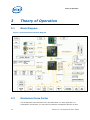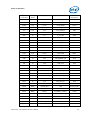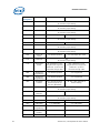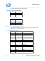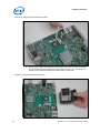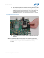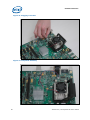
1
Intel® CoreTM 2 Duo processor
and Mobile Intel® GME965
Express Chipset
Development Kit User Manual
June 2007
Document Number: 316704-001
INFORMATION IN THIS DOCUMENT IS PROVIDED IN CONNECTION WITH INTEL® PRODUCTS. NO LICENSE, EXPRESS OR
IMPLIED, BY ESTOPPEL OR OTHERWISE, TO ANY INTELLECTUAL PROPERTY RIGHTS IS GRANTED BY THIS DOCUMENT. EXCEPT
AS PROVIDED IN INTEL'S TERMS AND CONDITIONS OF SALE FOR SUCH PRODUCTS, INTEL ASSUMES NO LIABILITY
WHATSOEVER, AND INTEL DISCLAIMS ANY EXPRESS OR IMPLIED WARRANTY, RELATING TO SALE AND/OR USE OF INTEL
PRODUCTS INCLUDING LIABILITY OR WARRANTIES RELATING TO FITNESS FOR A PARTICULAR PURPOSE, MERCHANTABILITY,
OR INFRINGEMENT OF ANY PATENT, COPYRIGHT OR OTHER INTELLECTUAL PROPERTY RIGHT. Intel products are not intended
for use in medical, life saving, life sustaining, critical control or safety systems, or in nuclear facility applications.
Intel may make changes to specifications and product descriptions at any time, without notice.
Intel Corporation may have patents or pending patent applications, trademarks, copyrights, or other intellectual property rights
that relate to the presented subject matter. The furnishing of documents and other materials and information does not provide
any license, express or implied, by estoppel or otherwise, to any such patents, trademarks, copyrights, or other intellectual
property rights.
Designers must not rely on the absence or characteristics of any features or instructions marked “reserved” or “undefined.” Intel
reserves these for future definition and shall have no responsibility whatsoever for conflicts or incompatibilities arising from
future changes to them.
Intel processor numbers are not a measure of performance. Processor numbers differentiate features within each processor
family, not across different processor families. See http://www.intel.com/products/processor_number for details.
The Intel® CoreTM 2 Duo processor and Mobile Intel® GME965 Express Chipset may contain design defects or errors known as
errata which may cause the product to deviate from published specifications. Current characterized errata are available on
request.
Contact your local Intel sales office or your distributor to obtain the latest specifications and before placing your product order.
Copies of documents which have an order number and are referenced in this document, or other Intel literature may be obtained
by calling 1-800-548-4725 or by visiting Intel's website at http://www.intel.com.
BunnyPeople, Celeron, Celeron Inside, Centrino, Centrino logo, Core Inside, Dialogic, FlashFile, i960, InstantIP, Intel, Intel logo,
Intel386, Intel486, Intel740, IntelDX2, IntelDX4, IntelSX2, Intel Core, Intel Inside, Intel Inside logo, Intel. Leap ahead., Intel.
Leap ahead. logo, Intel NetBurst, Intel NetMerge, Intel NetStructure, Intel SingleDriver, Intel SpeedStep, Intel StrataFlash, Intel
Viiv, Intel vPro, Intel XScale, IPLink, Itanium, Itanium Inside, MCS, MMX, Oplus, OverDrive, PDCharm, Pentium, Pentium Inside,
skoool, Sound Mark, The Journey Inside, VTune, Xeon, and Xeon Inside are trademarks or registered trademarks of Intel
Corporation or its subsidiaries in the United States and other countries.
*Other names and brands may be claimed as the property of others.
Copyright © 2007, Intel Corporation. All Rights Reserved.
2
316704-001 / Development Kit User’s Manual
Contents
1
About This Manual ............................................................................................6
1.1
1.2
1.3
1.4
1.5
1.6
2
Getting Started............................................................................................... 15
2.1
2.2
2.3
2.4
2.5
2.6
3
3.5
3.6
3.7
Block Diagram ..................................................................................... 24
Mechanical Form Factor......................................................................... 24
Thermal Management ........................................................................... 25
System Features and Operation.............................................................. 25
3.4.1
Mobile Intel® GME965 GMCH..................................................... 25
3.4.2
ICH8-M.................................................................................. 27
3.4.3
POST Code Debugger............................................................... 31
Clock Generation.................................................................................. 31
Power Management States..................................................................... 31
Power Measurement Support.................................................................. 33
Hardware Reference ........................................................................................ 39
4.1
4.2
4.3
4.4
4.5
4.6
Appendix A
Overview ............................................................................................ 15
2.1.1
Development Board Features .................................................... 15
Included Hardware and Documentation ................................................... 17
Software Key Features .......................................................................... 17
2.3.1
AMI BIOS ............................................................................... 18
Before You Begin.................................................................................. 18
Setting Up the Development Board ......................................................... 20
Configuring the BIOS ............................................................................ 22
Theory of Operation ........................................................................................ 24
3.1
3.2
3.3
3.4
4
Content Overview...................................................................................6
Text Conventions ...................................................................................6
Glossary of Terms and Acronyms ..............................................................8
Support Options ................................................................................... 13
1.4.1
Electronic Support Systems ...................................................... 13
1.4.2
Additional Technical Support ..................................................... 13
Product Literature................................................................................. 13
Related Documents............................................................................... 14
Primary Features.................................................................................. 39
Back Panel Connectors .......................................................................... 41
4.2.1
TV-Out D-Connector ................................................................ 42
Configuration Settings........................................................................... 43
Power On and Reset Buttons .................................................................. 47
LEDs .................................................................................................. 48
Other Headers, Slots and Sockets ........................................................... 49
4.6.1
H8 Programming Headers ......................................................... 49
4.6.2
Expansion Slots and Sockets..................................................... 50
. Heatsink Installation Instructions .................................................................... 64
316704-001 / Development Kit User’s Manual
3
Figures
Figure
Figure
Figure
Figure
Figure
Figure
Figure
Figure
Figure
Figure
Figure
Figure
Figure
Figure
Figure
1. Development Board Block Diagram....................................................... 24
2. Development Board Component Locations ............................................. 39
3. Back Panel Connector Locations ........................................................... 42
4. D-Connector to Component Video Cable ................................................ 43
5. D-Connector to Composite Video Cable ................................................. 43
6. D-Connector to S-Video Cable ............................................................. 43
7. Configuration Jumper and Switch Locations ........................................... 44
8. LED Locations ................................................................................... 48
9. Heatsink and Backplate ...................................................................... 64
10. Backplate Pins ................................................................................. 65
11. Applying the Thermal Grease ............................................................. 66
12. Squeezing Activation Arm.................................................................. 66
13. Installing the Heatsink ...................................................................... 67
14. Plugging in the Fan .......................................................................... 68
15. Completed Assembly ........................................................................ 68
Tables
Table
Table
Table
Table
Table
Table
Table
Table
Table
Table
Table
Table
Table
Table
Table
Table
Table
Table
Table
Table
Table
Table
Table
Table
Table
Table
Table
Table
Table
4
1. Text Conventions ..................................................................................7
2. Terms and Acronyms.............................................................................8
3. Acronyms ......................................................................................... 10
4. Intel Literature Centers........................................................................ 13
5. Related Documents ............................................................................. 14
6. Development Board feature Set Summary .............................................. 15
7. BIOS Location Strapping Options........................................................... 30
8. Primary System Clocks ........................................................................ 31
9. Power Management States ................................................................... 32
10. Power Management M-States .............................................................. 32
11. Sleep Signals and M-State Definition.................................................... 33
12. Development Board Voltage Rails ........................................................ 34
13. Development Board Component Location Legend ................................... 40
14. Back Panel Connector Definitions......................................................... 42
15. Supported Configuration Jumper/Switch Settings ................................... 44
16. LED Functions................................................................................... 48
17. Expansion Slots and Sockets............................................................... 50
18. PCI Express* (x16) Pinout (J6B2) ........................................................ 51
19. ADD2 Slot (J6B2) .............................................................................. 54
20. MEC Slot (J6B2)................................................................................ 57
21. PCI Express* (x1) Pinout (J6B1, J7B1, J8B4)......................................... 60
22. IDE Connector .................................................................................. 60
23. SATA Port 0 ‘Direct Connect’ Connector Pinout (J8J1) ............................. 61
24. SATA Ports 1 and 2 ‘Cable Connect’ Connector Pinout (J7J3, J7H1)........... 61
25. SATA Power Connection (J7H2) ........................................................... 62
26. Fan Connectors (J2B3, J2C1) .............................................................. 62
27. Fan Connector (J2F1) ........................................................................ 62
28. Front Panel Connector........................................................................ 62
29. USB Headers .................................................................................... 63
316704-001 / Development Kit User’s Manual
Revision History
Document
Number
Revision
Number
316704
001
Description
Initial public release.
Revision Date
June 2007
§
316704-001 / Development Kit User’s Manual
5
About This Manual
1
About This Manual
This user’s manual describes the use of the Intel® CoreTM 2 Duo processor and Mobile
Intel® GME965 Express Chipset development kit. This manual has been written for
OEMs, system evaluators, and embedded system developers. This document defines
all jumpers, headers, LED functions, and their locations on the development board,
along with subsystem features and POST codes. This manual assumes basic familiarity
in the fundamental concepts involved with installing and configuring hardware for a
personal computer system.
For the latest information about the Intel® CoreTM 2 Duo processor and Mobile Intel®
GME965 Express Chipset Development Kit, visit:
http://developer.intel.com/design/intarch/devkits/index.htm
For design documents related to this platform please visit:
Processor: http://developer.intel.com/design/intarch/core2duo/tech_docs.htm
Chipset:
1.1
http://www.intel.com/products/embedded/chipsets.htm
Content Overview
Chapter 1.0, “About This Manual” — This chapter contains a description of conventions
used in this manual. The last few sections explain how to obtain literature and contact
customer support.
Chapter 2.0, “Getting Started”— Provides complete instructions on how to configure
the development board and processor assembly by setting jumpers, connecting
peripherals and providing power.
Chapter 3.0, “Theory of Operation” — This chapter provides information on the system
design.
Chapter 4.0, “Hardware Reference”— This chapter provides a description of jumper
settings and functions, development board debug capabilities, and pinout information
for connectors.
Appendix A, “Heatsink Installation Instructions” gives detailed installation instructions
for the Intel® CoreTM 2 Duo processor heatsink.
1.2
Text Conventions
The notations listed in Table 1 may be used throughout this manual.
6
316704-001 / Development Kit User’s Manual
About This Manual
Table 1. Text Conventions
Notation
Definition
#
The pound symbol (#) appended to a signal name indicates that the signal
is active low. (e.g., PRSNT1#)
Variables
Variables are shown in italics. Variables must be replaced with correct
values.
Instructions
Instruction mnemonics are shown in uppercase. When you are
programming, instructions are not case-sensitive. You may use either
uppercase or lowercase.
Numbers
Units of Measure
A
GByte
KByte
KΩ
mA
MByte
MHz
ms
mW
ns
pF
W
V
µA
µF
µs
µW
Signal Names
Hexadecimal numbers are represented by a string of hexadecimal digits
followed by the character H. A zero prefix is added to numbers that begin
with A through F. (For example, FF is shown as 0FFH.) Decimal and binary
numbers are represented by their customary notations. (That is, 255 is a
decimal number and 1111 is a binary number. In some cases, the letter B
is added for clarity.)
The following abbreviations are used to represent units of measure:
amps, amperes
gigabytes
kilobytes
kilo-ohms
milliamps, milliamperes
megabytes
megahertz
milliseconds
milliwatts
nanoseconds
picofarads
watts
volts
microamps, microamperes
microfarads
microseconds
microwatts
Signal names are shown in uppercase. When several signals share a
common name, an individual signal is represented by the signal name
followed by a number, while the group is represented by the signal name
followed by a variable (n). For example, the lower chip-select signals are
named CS0#, CS1#, CS2#, and so on; they are collectively called CSn#.
A pound symbol (#) appended to a signal name identifies an active-low
signal. Port pins are represented by the port abbreviation, a period, and
the pin number (e.g., P1.0).
316704-001 / Development Kit User’s Manual
7
About This Manual
1.3
Glossary of Terms and Acronyms
Table 2 defines conventions and terminology used throughout this document.
Table 2. Terms and Acronyms
Term/Acronym
Definition
Aggressor
A network that transmits a coupled signal to another network.
Anti-etch
Any plane-split, void or cutout in a VCC or GND plane.
Assisted Gunning
Transceiver Logic+
The front-side bus uses a bus technology called AGTL+, or Assisted
Gunning Transceiver Logic. AGTL+ buffers are open-drain, and require
pull-up resistors to provide the high logic level and termination. AGTL+
output buffers differ from GTL+ buffers with the addition of an active
pMOS pull-up transistor to assist the pull-up resistors during the first clock
of a low-to-high voltage transition.
Asynchronous
GTL+
The processor does not utilize CMOS voltage levels on any signals that
connect to the processor. As a result, legacy input signals such as A20M#,
IGNNE#, INIT#, LINT0/INTR, LINT1/NMI, PWRGOOD, SMI#, SLP#, and
STPCLK# utilize GTL+ input buffers. Legacy output signals (FERR# and
IERR#) and non-AGTL+ signals (THERMTRIP# and PROCHOT#) also
utilize GTL+ output buffers. All of these signals follow the same DC
requirements as AGTL+ signals, however the outputs are not actively
driven high (during a logical 0 to 1 transition) by the processor (the major
difference between GTL+ and AGTL+). These signals do not have setup or
hold time specifications in relation to BCLK[1:0], and are therefore
referred to as “Asynchronous GTL+ Signals”. However, all of the
Asynchronous GTL+ signals are required to be asserted for at least two
BCLKs in order for the processor to recognize them.
Bus Agent
A component or group of components that, when combined, represent a
single load on the AGTL+ bus.
Crosstalk
The reception on a victim network of a signal imposed by aggressor
network(s) through inductive and capacitive coupling between the
networks.
Backward Crosstalk - Coupling that creates a signal in a victim network
that travels in the opposite direction as the aggressor’s signal.
Forward Crosstalk - Coupling that creates a signal in a victim network that
travels in the same direction as the aggressor’s signal.
Even Mode Crosstalk - Coupling from a signal or multiple aggressors when
all the aggressors switch in the same direction that the victim is switching.
Odd Mode Crosstalk - Coupling from a signal or multiple aggressors when
all the aggressors switch in the opposite direction that the victim is
switching.
Flight Time
Flight time is a term in the timing equation that includes the signal
propagation delay, any effects the system has on the TCO (time from
clock-in to data-out) of the driver, plus any adjustments to the signal at
the receiver needed to ensure the setup time of the receiver. More
precisely, flight time is defined as:
The time difference between a signal at the input pin of a receiving agent
crossing the switching voltage (adjusted to meet the receiver
8
316704-001 / Development Kit User’s Manual
About This Manual
Term/Acronym
Definition
manufacturer’s conditions required for AC timing specifications; i.e.,
ringback, etc.) and the output pin of the driving agent crossing the
switching voltage when the driver is driving a test load used to specify the
driver’s AC timings.
Maximum and Minimum Flight Time - Flight time variations are caused by
many different parameters. The more obvious causes include variation of
the board dielectric constant, changes in load condition, crosstalk, power
noise, variation in termination resistance, and differences in I/O buffer
performance as a function of temperature, voltage, and manufacturing
process. Some less obvious causes include effects of Simultaneous
Switching Output (SSO) and packaging effects.
Maximum flight time is the largest acceptable flight time a network will
experience under all conditions.
Minimum flight time is the smallest acceptable flight time a network will
experience under all conditions.
Infrared Data
Assoc.
The Infrared Data Association (IrDA) has outlined a specification for serial
communication between two devices via a bi-directional infrared data
port. The development board has such a port and it is located on the rear
of the platform between the two USB connectors.
IMVP6+
The Intel Mobile Voltage Positioning specification for the Intel® Core™ 2
Duo Processor. It is a DC-DC converter module that supplies the required
voltage and current to a single processor.
Inter-Symbol
Interference
Media Expansion
Card
Inter-symbol interference is the effect of a previous signal (or transition)
on the interconnect delay. For example, when a signal is transmitted down
a line and the reflections due to the transition have not completely
dissipated, the following data transition launched onto the bus is affected.
ISI is dependent upon frequency, time delay of the line, and the reflection
coefficient at the driver and receiver. ISI may impact both timing and
signal integrity.
The Media Expansion Card (MEC) provides digital display options through
the SDVO interface. The MEC card also incorporates video-in via a x1 PCI
Express* port.
Network
The network is the trace of a Printed Circuit Board (PCB) that completes
an electrical connection between two or more components.
Overshoot
The maximum voltage observed for a signal at the device pad, measured
with respect to VCC.
Pad
The electrical contact point of a semiconductor die to the package
substrate. A pad is only observable in simulations.
Pin
The contact point of a component package to the traces on a substrate,
such as the motherboard. Signal quality and timings may be measured at
the pin.
Power-Good
Ringback
“Power-Good,” “PWRGOOD,” or “CPUPWRGOOD” (an active high signal)
indicates that all of the system power supplies and clocks are stable.
PWRGOOD should go active at a predetermined time after system
voltages are stable and should go inactive as soon as any of these
voltages fail their specifications.
The voltage to which a signal changes after reaching its maximum
absolute value. Ringback may be caused by reflections, driver oscillations,
or other transmission line phenomena.
316704-001 / Development Kit User’s Manual
9
About This Manual
Term/Acronym
System Bus
Setup Window
Simultaneous
Switching Output
Definition
The System Bus is the microprocessor bus of the processor.
The time between the beginning of Setup to Clock (TSU_MIN) and the
arrival of a valid clock edge. This window may be different for each type of
bus agent in the system.
Simultaneous Switching Output (SSO) effects are differences in electrical
timing parameters and degradation in signal quality caused by multiple
signal outputs simultaneously switching voltage levels in the opposite
direction from a single signal or in the same direction. These are called
odd mode and even mode switching, respectively. This simultaneous
switching of multiple outputs creates higher current swings that may
cause additional propagation delay (“push-out”) or a decrease in
propagation delay (“pull-in”). These SSO effects may impact the setup
and/or hold times and are not always taken into account by simulations.
System timing budgets should include margin for SSO effects.
Stub
The branch from the bus trunk terminating at the pad of an agent.
Trunk
The main connection, excluding interconnect branches, from one end.
System
Management Bus
A two-wire interface through which various system components may
communicate.
Undershoot
The minimum voltage extending below VSS observed for a signal at the
device pad.
VCC (CPU core)
VCC (CPU core) is the core power for the processor. The system bus is
terminated to VCC (CPU core).
Victim
A network that receives a coupled crosstalk signal from another network is
called the victim network.
Table 3 defines the acronyms used throughout this document.
Table 3. Acronyms
Acronym
10
Definition
AC
Audio Codec
ACPI
Advanced Configuration and Power Interface
ADD2
Advanced Digital Display 2
ADD2N
Advanced Digital Display 2 Normal
AGTL
Assisted Gunning Transceiver Logic
AMC
Audio/Modem Codec.
ASF
Alert Standard Format
AMI
American Megatrends Inc. (BIOS developer)
ATA
Advanced Technology Attachment (disk drive interface)
ATX
Advance Technology Extended (motherboard form factor)
BGA
Ball Grid Array
316704-001 / Development Kit User’s Manual
About This Manual
Acronym
Definition
BIOS
Basic Input/Output System
CK-SSCD
Spread Spectrum Differential Clock
CMC
Common Mode Choke
CMOS
Complementary Metal-Oxide-Semiconductor
CPU
Central Processing Unit (processor)
DDR
Double Data Rate
DMI
Direct Memory Interface
ECC
Error Correcting Code
EEPROM
Electrically Erasable Programmable Read-Only Memory
EHCI
Enhanced Host Controller Interface
EMA
Extended Media Access
EMI
Electro Magnetic Interference
ESD
Electrostatic Discharge
EV
Engineering Validation
EVMC
Electrical Validation Margining Card
FCBGA
Flip Chip Ball Grid Array
FCPGA
Flip Chip Pin Grid Array
FIFO
First In First Out - describes a type of buffer
FS
Full-speed. Refers to USB
FSB
Front Side Bus
FWH
Firmware Hub
GMCH
Graphics Memory Controller Hub
HDA
High Definition Audio
HDMI
High Definition Media Interface
HS
High-speed. Refers to USB
ICH
I/O Controller Hub
IDE
Integrated Drive Electronics
IMVP
Intel Mobile Voltage Positioning
IP/IPv6
Internet Protocol/Internet Protocol version 6
IrDA
Infrared Data Association
ISI
Inter-Symbol Interference
KBC
Keyboard Controller
LAI
Logic Analyzer Interface
LAN
Local Area Network
LED
Light Emitting Diode
316704-001 / Development Kit User’s Manual
11
About This Manual
Acronym
12
Definition
LOM
LAN on Motherboard
LPC
Low Pin Count
LS
Low-speed. Refers to USB
LVDS
Low Voltage Differential Signaling
mBGA
Mini Ball Grid Array
MC
Modem Codec
MEC
Media Expansion Card
MHz
Mega-Hertz
OEM
Original Equipment Manufacturer
PCIe
PCI Express*
PCM
Pulse Code Modulation
POST
Power On Self Test
PLC
Platform LAN Connect
RAID
Redundant Array of Inexpensive Disks
RTC
Real Time Clock
SATA
Serial ATA
SIO
Super Input/Output
SKU
StockKeeping Unit
SMBus
System Management Bus
SODIMM
Small Outline Dual In-line Memory Module
SPD
Serial Presence Detect
SPI
Serial Peripheral Interface
SPWG
Standard Panels Working Group - http://www.spwg.org/
SSO
Simultaneous Switching Output
STR
Suspend To RAM
TCO
Total Cost of Ownership
TCP
Transmission Control Protocol
TDM
Time Division Multiplexed
TDR
Time Domain Reflectometry
µBGA
Micro Ball Grid Array
UDP
User Datagram Protocol
UHCI
Universal Host Controller Interface
USB
Universal Serial Bus
VGA
Video Graphics Adapter
VID
Voltage Identification
316704-001 / Development Kit User’s Manual
About This Manual
Acronym
Definition
VREG
Voltage Regulator
XDP
eXtended Debug Port
1.4
Support Options
1.4.1
Electronic Support Systems
Intel’s web site (http://www.intel.com/) provides up-to-date technical information and
product support. This information is available 24 hours per day, 7 days per week,
providing technical information whenever you need it.
1.4.2
Additional Technical Support
If you require additional technical support, please contact your Intel Representative or
local distributor.
1.5
Product Literature
In order to order hard copies of product literature the following instructions should be
followed:
1.
Determine the SKU Number
If you do not know the SKU # of the document you are ordering, please select
the back button to view the document again. The SKU # is the first 6 digits of
the number on the PDF file, such as: 12345612.pdf or at the bottom of the
download page for that document.
2.
Call, Mail or Email a request
Call: To place an order for a publication or text in hardcopy or CD form,
please contact our Intel® Literature Fulfillment Centers listed in Table 4.
Table 4. Intel Literature Centers
Location
Telephone Number
U.S. and Canada
1-800-548-4725
International
1-303-675-2148
Fax
1-303-675-2120
Mail a request to:
316704-001 / Development Kit User’s Manual
13
About This Manual
Intel Literature Fulfilment Center
P.O. Box 5937
Denver, Colorado 80217-9808
USA
Email a request to: [email protected]
Please make sure to include in your mailed/emailed request:
SKU #
Company Name
Your Name (first, last)
Full mailing address
Daytime Phone Number in case of questions
Note: Please be aware not all documents are available in all media types. Some may only be
available as a download.
1.6
Related Documents
Table 5 provides a summary of publicly available documents related to this
development kit. For additional documentation, please contact your Intel
Representative.
Table 5. Related Documents
Document Title
Location
Intel® Core™2 Duo Processor for Mobile
Intel® 965 Express Chipset Family
Datasheet
http://www.intel.com/design/mobile/datashts/316
745.htm
Mobile Intel® 965 Express Chipset Family
Datasheet
http://www.intel.com/design/mobile/datashts/316
273.htm
Intel® I/O Controller Hub 8 (ICH8) Family
Datasheet
http://www.intel.com/design/chipsets/datashts/3
13056.htm
Intel® Centrino® Pro processor technology
and Intel® Centrino® Duo processor
technology Design Guide For Intel®
Core™2 Duo Mobile Processor, Mobile
Intel® 965 Express Chipset Family and
Intel® 82801HBM ICH8M & Intel®
82801HEM ICH8M-E I/O Controller Hub
Based Systems
Contact your Intel representative for access to
this document
Intel® Core™2 Duo Mobile Processor,
Mobile Intel® 965 Express Chipset Family
and ICH8M I/O Controller Hub Schematics
Contact your Intel representative for access to
this document
§
14
316704-001 / Development Kit User’s Manual
Getting Started
2
Getting Started
This chapter identifies the development kit’s key components, features and
specifications. It also details basic development board setup and operation.
2.1
Overview
The development board consists of a baseboard populated with the Intel® CoreTM 2
Duo processor, the Mobile Intel® GME965 Express Chipset, other system board
components and peripheral connectors.
Note: The development board is shipped as an open system allowing for maximum flexibility
in changing hardware configuration and peripherals. Since the board is not in a
protective chassis, take extra precaution when handling and operating the system.
2.1.1
Development Board Features
Features of the development board are summarized in Table 6.
Table 6. Development Board feature Set Summary
Development Board
Implementation
Processor
Intel® CoreTM 2 Duo processor with
4 MByte L2 Cache on 65nm process
Comments
478 pin Flip Chip Pin Grid Array (MicroFCPGA) package
FSB 533/667/800 MHz support
Mobile Intel® GME965 Express
Chipset (GMCH)
1299-pin Micro-FCBGA Package
Intel® I/O Controller Hub 8-M
Enhanced (ICH8M-E)
676-pin BGA Package
A
T
Two DDR2 RAM SO-DIMM slots.
Maximum 4GB of DDR2 Memory (RAM)
using 1Gb technology and stacked SODIMMs.
F
E
U
R
Chipset
Memory
Supports DDR2 frequency of 533 or
667MHz
E
One PCI Express* Graphics Slot
One dual channel LVDS Connector
Video
One VGA Connector
One TV D-Connector supporting SVideo, Composite video and
Component video
PCI
One 5V PCI slot
316704-001 / Development Kit User’s Manual
The Mobile Intel® GME965 Express Chipset
(GMCH) has 2 video pipes which allows
support of dual independent display.
18-bpp and 24-bpp LVDS panel support
Support for two SDVO channels via x16
PCIe connector (through ADD2 or MEC
cards)
PCI revision 2.3 compliant (33MHz)
15
Getting Started
Development Board
Implementation
F
E
Comments
Three x1 connectors
Revision 1.1 compliant
One x16 connector
There are Five x1 PCI Express* slots but
slots 2 and 4 are not intended for use with
PCI Express* add-in cards. Only slots 1, 3
and 5 are supported.
On-Board LAN
10/100/1000 Mbps connectivity
from the Intel® 82566MM Gigabit
Platform LAN Connect component
The 82566MM is connected to the ICH via
the ICH’s GLCI and LCI interfaces.
SPI
Two 16Mbit devices
PCI Express*
A
T
U
R
E
PATA 33/66/100
1 Channel
3 SATA Ports
2 Cable Connector and 1 Direct Connect
Connector. RAID 0/1 support.
10 USB 2.0/1.1 Ports
Five ports provided on rear-panel, four
provided via headers (J6H3, J6H3) and
one via the PCI Express* docking
connector
LPC
One LPC slot
Includes sideband headers
BIOS
AMI BIOS installed in an 8Mb FWH
40-pin TSOP socket
Hitachi H8S/2104 micro-controller
ACPI compliant
ATA/Storage
USB
SMC/KBC
Two PS/2 ports
One scan matrix keyboard
connector
Clocks
CK-505 clock synthesizer and
DB800M clock buffer
Super I/O
SMSC SIO1007-JV
RTC
Battery-backed Real Time Clock
Thermal
Monitoring
Processor temperature sensor
Processor
Voltage
Regulator
IMVP-6+ for processor core
Power Supply
Supports IrDA and UART serial interfaces
Desktop Mode
ATX Power Supply
Mobile Mode
Battery Pack (smart battery support)
AC Mobile Brick
Debug
Interfaces
Intel® AMT
support
16
Port 80 display
Through Add-in card. Four seven-segment
displays
Extended Debug Port (XDP)
XDP connector
Intel® Active Management
Technology 2.5
Supported on the development board with
M0, M1, and M-off management states
316704-001 / Development Kit User’s Manual
Getting Started
Development Board
Implementation
ACPI Compliant
Comments
S0 – Power On
S3 – Suspend to RAM
S4 – Suspend to Disk
Power
Management
S5 – Soft Off
M0 – All Wells powered
M1 – Main Well down. Only ME power on
M-off – ME powered off
Form Factor
ATX 2.2 like form factor
10 layer board – 12” x 10.2”
Note: Review the document provided with the Development Kit titled “Important Safety and
Regulatory Information”. This document contains safety warnings and cautions that
must be observed when using this development kit.
2.2
Included Hardware and Documentation
The following hardware and documentation is included in the development kit:
2.3
•
One development board
•
One Intel® CoreTM 2 Duo processor with 4 MB L2 Cache on 65nm process in
the 478 pin Flip-Chip Pin Grid Array (Micro-FCPGA) package (Installed)
•
One Firmware Hub (FWH) (Installed)
•
One GMCH (GME965) heatsink (Installed)
•
One Type 2032, socketed 3 V lithium coin cell battery (Installed)
•
One 256 MByte DDR2 SODIMM (200 Pin)
•
One CPU thermal solution and CPU back plate (included in kit box – not
populated on board)
•
One cable kit
•
One Development Kit User’s Manual
•
One Port 80 add-in card
Software Key Features
The driver CD included in the kit contains all of the software drivers necessary for
basic system functionality under the following operating systems: Windows* XP/XP
Embedded, Vista and Linux*.
316704-001 / Development Kit User’s Manual
17
Getting Started
Note: While every care was taken to ensure the latest versions of drivers were provided on
the enclosed CD at time of publication, newer revisions may be available. Updated
drivers for Intel components can be found at:
http://developer.intel.com/design/intarch/software/index.htm
For all third-party components, please contact the appropriate vendor for updated
drivers.
Note: Software in the kit is provided free by the vendor and is only licensed for evaluation
purposes. Refer to the documentation in your evaluation kit for further details on any
terms and conditions that may be applicable to the granted licenses. Customers using
the tools that work with Microsoft* products must license those products. Any targets
created by those tools should also have appropriate licenses. Software included in the
kit is subject to change.
Refer to http://developer.intel.com/design/intarch/devkits for details on additional
software from other third-party vendors.
2.3.1
AMI BIOS
This development kit ships with AMI* BIOS pre-boot firmware from AMI* preinstalled. AMI* BIOS provides an industry-standard BIOS platform to run most
standard operating systems, including Windows* XP/XP Embedded, Linux*, and
others.
The AMI* BIOS Application Kit (available through AMI*) includes complete source
code, a reference manual, and a Windows-based expert system, BIOStart*, to enable
easy and rapid configuration of customized firmware for your system.
The following features of AMI* BIOS are enabled in the development board:
2.4
•
DDR2 SDRAM detection, configuration, and initialization
•
Mobile Intel® GME965 Express Chipset configuration
•
POST codes displayed to port 80h
•
PCI/PCI Express* device enumeration and configuration
•
Integrated video configuration and initialization
•
Super I/O configuration
•
CPU microcode update
•
Active Management Technology
•
RAID 0/1 Support
Before You Begin
The following additional hardware may be necessary to successfully set up and
operate the development board.
18
316704-001 / Development Kit User’s Manual
Getting Started
VGA Monitor: Any standard VGA or multi-resolution monitor may be used. The setup
instructions in this chapter assume the use of a standard VGA monitor, TV, or flat
panel monitor.
Keyboard: The development board can support either a PS/2 or USB style keyboard.
Mouse: The development board can support either a PS/2 or USB style mouse.
Hard Drives and Optical Disc Drives: Up to Three SATA drives and two IDE devices
(master and slave) may be connected to the development board. An optical disc drive
may be used to load the OS. All these storage devices may be attached to the board
simultaneously.
Video Adapter: Integrated video is output from the VGA connector on the back panel
of the development board. Alternately, a standard PCI Express* video adapter, ADD2
card or MEC video adapter may be used for additional display flexibility. Please contact
the respective vendors for drivers and necessary software for adapters not provided
with this development kit. Check the BIOS and the graphics driver, where appropriate,
for the proper video output settings.
Note: The enclosed driver CD includes drivers necessary for LAN, Integrated graphics, and
system INF utilities.
Network Adapter: A Gigabit network interface is provided on the development
board. The network interface will not be operational until after all the necessary
drivers have been installed. A standard PCI/PCI Express* adapter may be used in
conjunction with, or in place of, the onboard network adapter. Please contact the
respective vendors for drivers and necessary software for adapters not provided with
this development kit.
You must supply appropriate network cables to utilize the LAN connector or any other
installed network cards.
Power Supply: The development board has the option to be powered from two
different power sources: an ATX power supply or AC to DC adapter. The development
board contains all of the voltage regulators necessary to power the system.
There are two main supported power supply configurations, Desktop and Mobile. The
Desktop solution consists of only using the ATX power supply. The Mobile solution
consists of only using the AC to DC adapter.
Warning: The power supply cord is the main disconnect device to mains (AC power). The socket
outlet shall be installed near the equipment and shall be readily accessible.
Note: Desktop peripherals, including add-in cards, will not work in mobile power mode. If
desktop peripherals are used, the development board must be powered using desktop
power mode.
If using an ATX power supply, select a power supply that complies with the "ATX12V"
1.1 specification. For more information, refer to http://www.formfactors.org.
Note: If the power button on the ATX power supply is used to shut down the system, wait at
least five seconds before turning the system on again to avoid damaging the system.
316704-001 / Development Kit User’s Manual
19
Getting Started
Other Devices and Adapters: The development board functions much like a
standard desktop computer motherboard. Most PC-compatible peripherals can be
attached and configured to work with the development board.
2.5
Setting Up the Development Board
Once the necessary hardware (described in Section 2.4) has been gathered, follow the
steps below to set up the development board.
Note: To locate items discussed in the procedure below, please refer to Chapter 4.
1.
Create a safe work environment.
Ensure a static-free work environment before removing any components from
their anti-static packaging. The development board is susceptible to
electrostatic discharge (ESD) damage, and such damage may cause product
failure or unpredictable operation. A flame retardant work surface must also
be used.
Caution:
2.
It is recommended that an ESD wrist strap be used when handling the
development board.
Inspect the contents of your kit.
Check for damage that may have occurred during shipment. Contact your
sales representative if any items are missing or damaged.
20
Caution:
Since the development board is not in a protective chassis, use caution
when connecting cables to this product.
Caution:
Standby voltage is constantly applied to the development board. Remove
power before any hardware (peripherals, keyboards, mice, monitors,
accessories, add-in cards, etc) is added or removed from the board.
Note:
The development board is a standard ATX form factor. An ATX chassis may
be used if a protected environment is desired. If a chassis is not used,
standoffs must be used to elevate the development board off the working
surface to protect the memory and board components from any
accidental contact to metal objects.
3.
Check the jumper default position setting. Refer to Figure 7 for jumper location.
Jumper J5H2 is used to clear the CMOS memory. Make sure this jumper is set to
1-x for normal operation.
4.
Be sure to populate the following hardware on your development board:
•
One Intel® CoreTM 2 Duo processor
•
One processor thermal solution
•
One 256 MByte DDR2 667 SODIMM (200-pin) into connector J5P1.
316704-001 / Development Kit User’s Manual
Getting Started
Note:
Ensure that the processor has been locked into the socket by turning the
socket screw fully clockwise.
Note:
For proper installation of the CPU thermal solution, please refer
to Appendix A
5.
Connect a SATA or IDE hard disk drive.
6.
Connect any additional storage devices to the development board.
7.
Connect the keyboard and mouse.
Connect a PS/2-style or USB mouse and keyboard (see Figure 3 on page 38
for connector locations).
Note:
J1A1 (on the baseboard) is a stacked PS/2 connector. The bottom
connector is for the keyboard and the top is for the mouse.
8.
Connect an Ethernet cable (optional).
9.
Connect the monitor through the VGA connector.
10. Connect the power supply.
Connect an appropriate power supply to the development board. Make sure
the power supply is not plugged into an electrical outlet (turned off). After
connecting the power supply board connectors, plug the power supply cord
into an electrical outlet.
11. Power up the development board.
Power and Reset are implemented on the development board through buttons
located on SW1C1 and SW1C2, respectively. See Figure 7 for switch locations.
Turn on the power to the monitor and development board. Ensure that the
fansink on the processor is operating.
Note:
The power button may have to be pressed twice to turn the power on.
12. Install operating system and necessary drivers.
Depending on the operating system chosen, all necessary drivers for
components included in this development kit can be found on the enclosed
CD. Please see Section 2.3 for information on obtaining updated drivers.
2.6
Configuring the BIOS
AMI* BIOS is pre-loaded on the development board. The default BIOS settings may
need to be modified to enable/disable various features of the development board. The
BIOS settings are configured through a menu-driven user interface which is accessible
during the Power On Self Test (POST). The Delete key on the attached keyboard
should be pressed during POST to enter the interface. For AMI BIOS POST codes, visit:
http://www.ami.com
For BIOS Updates please contact your Intel Sales Representative.
§
316704-001 / Development Kit User’s Manual
21
Theory of Operation
3
Theory of Operation
3.1
Block Diagram
Figure 1. Development Board Block Diagram
3.2
Mechanical Form Factor
The development board conforms to the ATX form factor. For extra protection in a
development environment, you may want to install the development board in an ATX
22
316704-001 / Development Kit User’s Manual
Theory of Operation
chassis. Internal and rear panel system I/O connectors are described in Section 3.4.
An overview of connector and slot locations is provided in Chapter 4.
3.3
Thermal Management
The objective of thermal management is to ensure that the temperature of each
component is maintained within specified functional limits. The functional temperature
limit is the range within which the electrical circuits can be expected to meet their
specified performance requirements. Operation outside the functional limit can
degrade system performance and cause reliability problems.
The development kit is shipped with a heatsink thermal solution for installation on the
processor. This thermal solution has been tested in an open-air environment at room
temperature and is sufficient for development purposes. The designer must ensure
that adequate thermal management is provided for if the system is used in other
environments or enclosures.
3.4
System Features and Operation
The following section provide a detailed view of the system features and operation of
the development board.
3.4.1
Mobile Intel® GME965 GMCH
The Mobile Intel® GME965 Express Chipset GMCH provides the processor interface
optimized for Intel® CoreTM 2 Duo processors, system memory interface, DMI and
internal graphics. It provides flexibility and scalability in graphics and memory
subsystem performance. The following list describes the development board’s
implementation of the Mobile Intel® GME965 Express Chipset GMCH features.
A list of features follows:
•
1299-ball Micro-FCBGA package
•
533/667/800 MHz Front Side Bus
•
36-bit host bus addressing
•
System memory controller (DDR2 implemented)
o
Supports Dual Channel and Single Channel operation
o
Two 200-pin SODIMM slots
o
DDR2 533/667
•
Direct Media Interface (DMI)
•
Integrated graphics based on the Intel Graphics Media Accelerator X3100
o
Directly supports on-board VGA, TV D-Connector and LVDS interfaces.
316704-001 / Development Kit User’s Manual
23
Theory of Operation
•
SDVO interface via PCI Express* x16 connector provides maximum display
flexibility
o
3.4.1.1
Can drive up to two display outputs
System Memory
The development board supports DDR2 533/667 main memory. Two 200-pin SODIMM
connectors (one per channel) on the development board support unbuffered, non-ECC,
single and double-sided DDR2 533/667 MHz SODIMMs. These SODIMMs provide the
ability to use up to 1 Gbit technology for a maximum of 4 GBytes system memory.
Note: Memory that utilizes 128 MBit technology is not supported on the Mobile Intel®
GME965 Express Chipset.
Note: The SODIMM connectors are on the back side of the development board.
Caution:
3.4.1.2
Standby voltage may be applied to the SODIMM sockets when the system is in the
S3, S4 and S5 states. Therefore, do not insert or remove SODIMMs unless the
system is unplugged.
DMI
The Mobile Intel® GME965 Express Chipset GMCH’s Direct Media Interface (DMI)
provides high-speed bi-directional chip-to-chip interconnect for communication with
the ICH8-M.
3.4.1.3
Advanced Graphics and Display Interfaces
The development board has five options for displaying video: VGA, LVDS, TV-Out,
SDVO, or PCI Express* Graphics. SDVO and PCI Express* Graphics are multiplexed on
the same pins within the Mobile Intel® GME965 Express Chipset. The development
board contains one SDVO/PCI Express* Graphics Slot (J6B2) for a PCI Express*
compatible graphics card or an SDVO compatible graphics card, one LVDS connector
(J6F1), one TV-Out connector (J2A1), and one 15-pin VGA connector (J2A2).
3.4.1.3.1
VGA Connector
A standard 15 pin D-Sub connector on the rear panel provides access to the analog
output of the Mobile Intel® GME965 Express Chipset. This can be connected to any
capable analog CRT or flat panel display with compatible input.
When used in conjunction with the other display options, the displays can operate in
Dual Independent mode. This allows unique content to appear on each display at
unique refresh rates and timings.
3.4.1.3.2
LVDS Flat Panel Interface
The development board provides one 50-pin LVDS video interface connector. The
interface is compliant with the SPWG 3.5 (for 18-bpp panels) and proposed SPWG 4.0
(for 24-bpp panels) standards.
24
316704-001 / Development Kit User’s Manual
Theory of Operation
3.4.1.4
PCI Express x16 Slot
The development board provides access to one x16 PCI Express* connector. Any
industry standard x1 or x16 PCI Express* video adapter may be used with this
interface. Additionally, any industry standard non-graphics x1, x4 or x8 adapter may
also be used. x2 adapters are not part of the PCI Express* specification but x2 nongraphics devices are also supported.
Note: The AMI BIOS that is included with the development board is configured to allow x2,
x4 and x8 non-graphics support through the x16 PCI Express* connector. If the user
wishes to use another BIOS on the development board then the BIOS may need to be
modified to support this feature.
3.4.2
ICH8-M
The ICH8-M is a highly integrated multifunctional I/O controller hub that provides the
interface to the system peripherals and integrates many of the functions needed in
today’s PC platforms. The following sections describe the development board
implementation of the ICH8-M features, which are listed below:
3.4.2.1
•
Three PCI Express* (x1) connectors
•
One PCI connectors
•
LPC interface
•
System Bus Management
•
ACPI* 3.0 compliant
•
Real Time Clock
•
676-ball mBGA package
•
Three SATA drive connectors
•
One IDE connector
•
Ten Universal Serial Bus (USB) 2.0 ports (five ports provided on rear-panel,
four provided via headers (J6H3, J6H4) and one on the docking connector.
PCI Express* Slots
The development board has three x1 PCI Express* slots for add-in cards. The PCI
Express* interface is compliant to the PCI Express* Rev. 1.1 Specification.
Note: There are actually Five x1 PCI Express* slots but slots 2 and 4 are not intended for
use with PCI Express* add-in cards. Only slots 1, 3 and 5 are supported.
3.4.2.2
PCI Slots
The development board has one 5V PCI slot for add-in cards. The PCI bus is compliant
to the PCI Rev. 2.3 Specification at 32-bit/33 MHz
316704-001 / Development Kit User’s Manual
25
Theory of Operation
3.4.2.3
On-Board LAN
The development board has one RJ-45 interface – at connector J5A1 - through which
10/100/1000 ethernet is available. The ethernet MAC is located in the ICH8-M and the
PHY is located externally in the 82566MM LAN Connect Interface (LCI) device. The
82566MM is connected to the ICH8-M via two interfaces: LCI for 10/100 Mbps traffic
and GLCI (Gigabit LCI) for 1000Mbps traffic. Intel® Active Management Technology is
optionally supported through these components.
Information on Intel® Active Management Technology can be found at:
http://www.intel.com/technology/manage/iamt/
Note: Further details on the location of the RJ-45 interface can be found in Section 4.2.
3.4.2.4
High Definition Audio
Intel® High Definition Audio is not supported on the development board.
3.4.2.5
ATA/ Storage
The development board has one parallel ATA IDE connector and three serial ATA
connectors.
The parallel ATA IDE Connector is a standard 40-pin connector at J7J4. This connector
supports up to two Ultra ATA/100 hard drives; one master and one slave.
There are three SATA connectors on the development board – one ‘Direct Connect’
connector and two ‘Cable Connect’ connectors. The ‘Direct Connect’ connector, located
at J8J1, provides both signaling and power while the ‘Cable Connect’ connectors,
located at J7H1 and J7J3, only provides signals (the user typically uses an ATX power
supply for the drive power). A green LED at location CR6J1 indicates activity on the
ATA channel.
The development board also supports ‘ATA swap’ capability for both the parallel IDE
channel and the serial ATA channels. A device can be powered down by software and
the port can then be disabled, allowing removal and insertion of a new device. The
parallel IDE device should be powered from the power connector, J4J2, on the
development board to utilize the hot swap feature. This feature requires customerdeveloped software support.
Note: Desktop hard drives must be powered using the external ATX power supply, not the
onboard power supply.
The Mobile Intel® GME965 Express Chipset includes Intel® Matrix Storage Technology,
providing greater performance and reliability through features such as Native
Command Queuing (NCQ) and RAID 0/1. For more information about Intel® Matrix
Storage Technology, refer to Intel’s website at:
http://www.intel.com/design/chipsets/matrixstorage_sb.htm
3.4.2.6
USB Connectors
The ICH8-M provides a total of ten USB 2.0 ports. Three ports are routed to a triplestack USB connector at J3A1. Two ports are routed to a combination RJ-45/dual USB
26
316704-001 / Development Kit User’s Manual
Theory of Operation
connector at J5A1. Four ports are routed to USB front panel headers at J6H3 and
J6H4. The last is routed to the PCI-Express* docking connector at J9C1.
There are Five UHCI Host Controllers and two EHCI Host Controllers. Each UHCI Host
Controller includes a root hub with two separate USB ports each, for a total of ten
legacy USB ports. The first EHCI Host Controller includes a root hub that supports up
to six USB 2.0 ports and the second EHCI Host Controller includes a root hub that
supports up to four USB 2.0 ports.
The connection to either the UHCI or EHCI controllers is dynamic and dependant on
the particular USB device. As such, all ports support High Speed, Full Speed, and Low
Speed (HS/FS/LS).
3.4.2.7
LPC Super I/O (SIO)/LPC Slot
An SMSC SIO1007-JV serves as the SIO on the development board. Shunting the
jumper at J7D1 to the 2-3 positions can disable the SIO by holding it in reset. This
allows other SIO solutions to be tested in the LPC slot at J8E1. A sideband header is
provided at J9G1 for this purpose. This sideband header also has signals for LPC
power management. Information on this header is on sheet 44 of the development
board schematics.
3.4.2.8
Serial, IrDA
The SMSC SIO incorporates a serial port, and IrDA (Infrared), as well as general
purpose IOs (GPIO). The Serial Port connector is provided at J2A2, and the IrDA
transceiver is located at U4A1. The IrDA transceiver on the development board
supports SIR (slow IR), FIR (Fast IR) and CIR (Consumer IR). The option to select
between these is supported through software.
3.4.2.9
BIOS Firmware Hub (FWH)
An 8-Mbit Flash device used on the development board to store system and video. The
reference designator location of the FWH device is U8G1. The BIOS can be upgraded
using an MS-DOS* based utility called FWHFlash and is addressable on the LPC bus off
of the ICH8-M. FWHFlash is available on request from your Intel representative.
3.4.2.10
SPI
The Serial Peripheral Interface on ICH8-M is used to support two compatible flash
devices at locations U7E1 and U6D2. By default, the SPI flash is used to store
configuration data for the LAN controller. Optionally it may be used for BIOS and AMT
firmware storage.
It is necessary to set certain strapping options to enable either a FWH-based or SPIbased BIOS. Optionally, it is also possible to direct BIOS access to the PCI interface.
Table 7 describes these strapping options.
316704-001 / Development Kit User’s Manual
27
Theory of Operation
Table 7. BIOS Location Strapping Options
ICH8-M Signal
GNT#0
SPI_CS1#
BIOS Location
0
1
SPI
1
0
PCI
1
1
LPC (Default)
Note: GNT#0 is configurable via jumper J8E2. Further details on its location can be found in
Section 4.3. SPI_CS1# is configurable via stuffing option R7U12. By default R7U12 is
not stuffed resulting in a SPI_CS1# strapping value of 1.
3.4.2.11
System Management Controller (SMC)/Keyboard Controller
The Hitachi* H8S/2104RV serves as both SMC and KBC for the development board.
The SMC/KBC controller supports two PS/2 ports, battery monitoring and charging,
EMA support, wake/runtime SCI events, and power sequencing control. The two PS/2
ports on the development board are for legacy keyboard and mouse. The keyboard
plugs into the bottom jack and the mouse plugs into the top jack at J1A1. Scan matrix
keyboards can be supported via an optional connector at J9E1.
3.4.2.12
Clocks
The development board uses a CK-505 clock synthesizer and DB800 clock buffer
compatible solution. The FSB frequency is determined from decoding the processor
BSEL[2:0] pin settings. This pin settings may be strapped using the jumpers at J1G2,
J1G5 and J1G8. Refer to Figure 7 and Table 15 for further information on these
jumpers.
3.4.2.13
Real Time Clock
An on-board battery at BT5H1 maintains power to the real time clock (RTC) when in a
mechanical off state. A CR2032 battery is installed on the development board.
Warning: Risk of explosion if the lithium battery is replaced by an incorrect type. Dispose of
used batteries according to the vendor's instructions.
3.4.2.14
Thermal Monitoring
The processor has a thermal diode for temperature monitoring. The SMC throttles the
processor if it becomes hot. If the temperature of the processor rises too high, the
SMC alternately blinks the CAPS lock and NUM lock LEDs on the development board,
and the development board shuts down.
A 3-pin fan header J3C1 is provided to support Tachometer output measurement for
GMCH. The development board supports PWM based speed control. As part of the
thermal measurement, the speed of the fan is varied based on the temperature
measurement.
28
316704-001 / Development Kit User’s Manual
Theory of Operation
3.4.3
POST Code Debugger
A Port 80-83 Add-in card can be plugged into to the development board at the TPM
header (J9A1). This card decodes the LPC bus BIOS POST codes and displays them on
four 7-segment LED displays.
For AMI* BIOS POST codes, please visit: http://www.ami.com
3.5
Clock Generation
The development board uses a CK-505 and DB800 compatible solution. The FSB
frequency is determined from decoding the processor BSEL[2:0] pin settings.
The clock generator provides Processor, GMCH, ICH8-M, PCI, PCI Express*, SATA, and
USB reference clocks. Clocking for DDR2 is provided by the GMCH.
Table 8. Primary System Clocks
Clock Name
3.6
Speed
CPU
133 MHz @ 533 FSB Speed
166 MHz @ 667 FSB Speed
200 MHz @ 800 FSB Speed
DDR2
133 MHz @ 533 Memory Speed
166 MHz @ 667 Memory Speed
PCI Express* and DMI
100 MHz
SATA
100MHz
PCI
33MHz
USB
48MHz
Super I/O
14MHz
Power Management States
Table 9 and Table 10 lists the power management states that have been defined for
the baseboard.
The Manageability Engine (ME) operates at various power levels, called M-states. M0
is the highest power state, followed by M1 and M-off. The Manageability Engine
provides some of the functionality required to implement Intel® Active Management
Technology (iAMT) on the development board. Further information on iAMT can be
found here: http://www.intel.com/technology/manage/iamt/
Table 9. Power Management States
State
Description
G0/S0/C0
Full on
G0/S0/C2
STPCLK# signal active
316704-001 / Development Kit User’s Manual
29
Theory of Operation
State
Description
G0/S0/C3
Deep Sleep: DPSLP# signal active
G0/S0/C4
Deeper Sleep: DPRSLP# signal active
G1/S3
Suspend To RAM (all switched rails are turned off)
G1/S4
Suspend To Disk
G2/S5
Soft Off
G3
Mechanical Off
Table 10. Power Management M-States
MState
Description
M0
Full on. All
manageability
functions
supported
M1
M-off
Main
System
Memory
Subsystem1
Manageability
Subsystem2
Clocks
Powered
Powered and
active
Powered
Powered
Manageability
functions that only
require memory
are supported
Off
Powered - Self
refresh.
Powered
Only
BCLK pair
to MCH is
active3
Manageability is
disabled
Off
Off
Off
Off
NOTES:
1.
Memory subsystem is the memory and memory-related power supplies to the MCH.
2.
Manageability Subsystem includes manageability functions in the chipset, SPI flash, and
LAN devices.
3.
In M1 the clock is powered, however only the BCLK pair to the MCH is active.
Everything besides the PLL in the clock chip is disabled and powered down.
Note: While in an M-state other than M-off, the traditional hardware definition of the S-State
as defined by the SLP signals is overridden by the ICH8M. This allows devices
controlled by SLP_S3# and SLP_S4#, such as system memory, to be available to the
Manageability system as needed. Even though the SLP signals may be driven
differently in M-States, the S-State information is retained in the ICH8M for transition
to M-off. S4_STATE# is the new signal to indicate S4 transition.
Table 11 provides a truth table of the SLP signals in various system states and MStates. The ICH8M provides all of the SLP signals shown in the table below.
30
316704-001 / Development Kit User’s Manual
Theory of Operation
Table 11. Sleep Signals and M-State Definition
State
Signal
3.7
SLP_S3#
SLP_S4#
SLP_S5#
S4_STATE#
SLP_M#
S0/M0
High
High
High
High
High
S3/M1
Low
High
High
High
High
S4/M1
Low
High
High
Low
High
S5/M1
Low
High
Low
Low
High
S3/M-off
Low
High
High
High
Low
S4/M-off
Low
Low
High
Low
Low
S5/M-off
Low
Low
Low
Low
Low
S0 (Non-AMT)
High
High
High
High
High
S3 (Non-AMT)
Low
High
High
High
Low
S4 (Non-AMT)
Low
Low
High
Low
Low
S5 (Non-AMT)
Low
Low
Low
Low
Low
Power Measurement Support
Power measurement resistors are provided on the development board to measure the
power of most subsystems. All power measurement resistors have a tolerance of 1%.
The value of these power measurement resistors are 0.002Ω by default. Power on a
particular subsystem is calculated using the following formula:
P=
V2
R
R = value of the sense resistor (typically 0.002Ω)
V = the voltage difference measured across the sense resistor
Use of an oscilloscope or high precision digital multi-meter tool such as the Agilent*
34401A digital multi-meter is recommended. Meters such as this have 6½ digits of
accuracy and can provide a much greater accuracy in power measurement than a
common 3½ digit multi-meter.
Table 12 summarizes all the power measurement resistors located on the
development board. All resistors are 0.002 Ω unless otherwise noted. Reference
designators marked with an asterisk are “not stuffed” on the development board.
316704-001 / Development Kit User’s Manual
31
Theory of Operation
Table 12. Development Board Voltage Rails
32
Component
/ Interface
Voltage
Plane
Supply
Rail
Reference
Designator
CPU VR
5V
+V5S
+V5S_IMVP6
R1B1
CPU VR
Battery
+VBAT
+VDC_PHASE
R2P12
CPU VR
Variable
6208_1_PHASE_LOUT
+VCC_CORE
R3D1
CPU VR
Variable
6208_2_PHASE_LOUT
+VCC_CORE
R2D1
CPU VR
Variable
6208_3_PHASE_LOUT
+VCC_CORE
R2D2
CPU
1.05V
+V1.05S
+V1.05S_CPU
R3T2* and R3R7*
CPU
1.5V
+V1.5S
+VCCA_PROC
R3U1 (0.01Ω)
GMCH VR
Battery
+VBATA
1.5S_VIN
R5V3
GMCH VR
Battery
+VBATA
VGMCH_IN
R5F16
GMCH VR
5V
+V5S
+V5S_GVR
R3F12
GMCH VR
Battery
+VBAT
GVR_VBAT
R3V2
GMCH VR
3.3V
V3.3S_TVDAC_R2
+V3.3S_TVDAC
R3E2 (0.01Ω)
GMCH VR
Battery
+VBATA
V1.25M_VIN
R4V4
GMCH VR
1.05 V
+V1.05OUT
+V1.05M
R4F13 (0.01Ω)
GMCH
1.05V
+V1.05S
+VCC_GMCH
R6E1
GMCH
VCCP
(1.05V)
+V1.05S
+VCCP_GMCH
R5U26
GMCH
1.05V
+V1.05S
+VCC_PEG
R6T14
GMCH
1.25S
+V1.25S
+VCC_PEG
R6T13*
GMCH
1.05V
+V1.05S
+VCC_DMI
R6T11
GMCH
1.25S
+V1.25S
+VCC_DMI
R6E2*
GMCH
1.05V
+V1.05M
+VCC_AXM
R6R1
GMCH
V_GFX
(1.05S)
+VCC_GFXCORE
+VCC_GFX
R3F8
GMCH
1.25V
+V1.25S
+V1.25S_PEGPLL
R5E3
GMCH
1.25V
+V1.25M
+V1.25M_A_SM_CK
R5P5
GMCH
1.25V
+V1.25S
+V1.25S_DMI
R6D5
GMCH
1.25V
+V1.25S
+V1.25S_MCH_PLL
R5U24
GMCH
1.25V
+V1.25M
V1.25M_MCH_PLL2
R4D6
GMCH
1.25V
+V1.25M
+V1.25M_A_SM
R4R2
GMCH
1.25V
+V1.25M
+V1.25M_AXD
R4C27
GMCH
1.25V
+V1.25S
+V1.25S_AXF
R4F9
GMCH
1.5V
+V1.5S
TVDAC_FB
R5U8
316704-001 / Development Kit User’s Manual
Theory of Operation
Component
/ Interface
Voltage
Plane
Supply
Rail
Reference
Designator
GMCH
1.8V
+V1.8
+V1.8_GMCH
R5D1
GMCH
1.8V
+V1.8_GMCH
+V1.8_SM_CK
R5D2
GMCH
1.8V
+V1.8
+V1.8_TXLVDS
R5U25
GMCH
1.8V
+V1.8
+V1.8_DLVDS
R5E5
GMCH
3.3V
+V3.3S
+V3.3S_HV
R5U2
GMCH
3.3V
+V3.3S
+V3.3S_SYNC
R5F9
GMCH
3.3V
+VCCA_TVDAC
+V3.3S_DAC_BG
R5U19 (0.03Ω)
GMCH
3.3V
+V3.3S
+V3.3S_PEG_BG
R6E3
PCI-E Gfx
3.3V
+V3.3S
+V3.3S_PEG
R6C1
PCI-E Gfx
3.3V
+V3.3
+V3.3S_PEG
R6P2*
PCI-E Gfx
Battery
+VBATS
+V12S_PEG
R6N9
PCI-E Gfx
Battery
+VBAT_S4
+V12S_PEG
R6N5*
ICH
1.05V
+V1.05S
+V1.05S_ICH
R7F12
ICH
1.05V
+V1.05S
+V1.05S_ICH_IO
R6V11
ICH
1.25V
+V1.25S
+V1.25S_DMI_ICH
R6G3
ICH
1.5V
+V1.5S
+V1.5S_PCIE_ICH
R6F13
ICH
1.5V
+V1.5S
+V1.5S_SATA_ICH
R8G2
ICH
1.5V
+V1.5S
+V1.5S_USB_ICH
R8F7
ICH
1.5V
+V1.5S
+V1.5S_APLL_ICH
R8G2
ICH
3.3V
+V3.3S
+V3.3S_DMI_ICH
R6G4
ICH
3.3V
+V3.3S
+V3.3S_GLAN_ICH
R6F2
ICH
3.3V
+V3.3M
+V3.3M_ICH
R7U3
ICH
3.3V
+V3.3A
+V3.3A_ICH
R6V12
ICH
3.3V
+V3.3A
+V3.3A_USB_ICH
R8F4
ICH
3.3V
+V3.3S
+V3.3S_IDE_ICH
R8G1
ICH
3.3V
+V3.3S
+V3.3S_VCCPCORE_ICH
R8V14
ICH
3.3V
+V3.3M
+V3.3M_VCCPAUX
R7F1
ICH
3.3V
+V3.3S
+V3.3S_PCI_ICH
R8F5
ICH
3.3V
+V3.3S
+V3.3S_SATA_ICH
R8G7
ICH
3.3V
+V3.3S_1.5S_HDA_IO
+V3.3S_1.5S_HDA_IO_IC
H
R7V4 (0.022Ω)
Memory
Battery
+VBATA
1.8_VIN
R5N13
Memory
0.9 V
+V0.9
+V0.9_R
R4B13
Memory
1.8V
+V1.8
+V1.8_DIMM0
R5C2
316704-001 / Development Kit User’s Manual
33
Theory of Operation
34
Component
/ Interface
Voltage
Plane
Supply
Rail
Reference
Designator
Memory
1.8V
+V1.8
+V1.8_DIMM1
R5B10
Memory
3.3V
+V3.3M
+V3.3M_DIMM0
R4C1 (0.022Ω)
Memory
3.3V
+V3.3M
+V3.3M_DIMM1
R4B26 (0.022Ω)
LAN
3.3V
+V3.3M_LAN_SW
+V3.3M_LAN
R6A23
LAN
1.8V
+V1.8_LAN
+V1.8_LAN_M
R6M1
LAN
1V
+V1.0_LAN_M
+V1.0_LAN_M_IN
R6M3
PCI
3.3V
+V3.3S
+V3.3S_PCI
R9D2
PCI
3.3V
+V3.3
+V3.3_PCISLT3
R8C5*
PCI
3.3V
+V3.3S_PCI
+V3.3_PCISLT3
R9D3
PCI
5V
+V5S
+V5S_PCI
R9B1
PCI
5V
+V5
+V5_PCISLT3
R8B3*
PCI
5V
+V5S_PCI
+V5_PCISLT3
R9B2
PCI
5V
+V5
+V5_PCI
R9A11*
PCI
12V
+V12S
+V12S_PCI
R8B1
PCI-E
12V
+V12S
+V12S_PCIESLOT1
R7N11
PCI-E
12V
+V12S
+V12S_PCIESLOT2
R7C20
PCI-E
12V
+V12S
+V12S_PCIESLOT3
R8B2
PCI-E
12V
+V12S
+V12S_PCIESLOT4
R8C7
PCI-E
12V
+V12S
+V12S_PCIESLOT5
R7N9
PCI-E
3.3V
+V3.3S
+V3.3S_PCIESLOT1
R7N10
PCI-E
3.3V
+V3.3S
+V3.3S_PCIESLOT2
R7R1
PCI-E
3.3V
+V3.3S
+V3.3S_PCIESLOT3
R7N5
PCI-E
3.3V
+V3.3S
+V3.3S_PCIESLOT4
R8D2
PCI-E
3.3V
+V3.3S
+V3.3S_PCIESLOT5
R7N8
Audio
3.3 V
+V3.3S
+V3.3S_1.5S_HDA_IO
R7W5
Audio
1.5 V
+V1.5S
+V3.3S_1.5S_HDA_IO
R7H6*
Audio
1.5 V
+V1.5A_HDA_IO
+V3.3A_1.5A_HDA_IO
R8E8*
Audio
3.3 V
+V3.3A
+V3.3A_1.5A_HDA_IO
R8E7
Panel Bklt
5V
+V5S
+V5S_LVDS_BKLT
R6U8
Panel Bklt
Battery
+VBAT
+VCC_LVDS_BKLT
R6F1
Panel LVDS
3.3V
+V3.3S
+V3.3S_L
R6U13
Panel LVDS
5V
+V5S
+V3.3S_L
R6U16*
Panel LVDS
3.3V
+V3.3S
+V3.3S_LVDS_DDC
R6F9
316704-001 / Development Kit User’s Manual
Theory of Operation
Component
/ Interface
Voltage
Plane
Supply
Rail
Reference
Designator
Panel LVDS
5V
+V5S
+V3.3S_LVDS_DDC
R6U9*
CK505
3.3V
+V3.3M_CK505
VDD_CK505
R5G11
CK505
3.3V
+V3.3S
+V3.3S_DB800
R7C10
CK505
0.9V
IO_VOUT_D
+VDDIO_CLK
R5V11
LPC
3.3V
+V3.3
+V3.3_LPCSLOT
R8F2
LPC
5V
+V5
+V5_LPCSLOT
R8E2
TPM
5V
+V5
V5_R1_TPM
R9M7
TPM
3.3V
+V3.3S
V3.3S_R1_TPM
R9M8
TPM
3.3V
+V3.3A
V3.3A_R1_TPM
R9A8
SMC
3.3V
+V3.3A
+V3.3A_KBC
R8H1
PS2
5V
+V5
+V5_PS2
R1A1
SIO
3.3V
+V3.3S
+V3.3S_SIO
R7E1
IR
3.3V
+V3.3S
+V3.3S_IR
R4M3
FWH
3.3V
+V3.3S
+V3.3S_FWH
R8V17
USB
5V
+V5A
+V5A_USBPWR_IN1
R5W9
USB
5V
+V5A
+V5A_USBPWR_IN2
R7H7
USB
5V
+V5A
+V5A_USBPWR_IN3
R3B5
IDE
5V
+V5S
+V5S_PATA
R5Y6
IDE
12V
+V12S
+V12S_PATA
R3Y2
SPI
3.3V
+V3.3M
+V3.3M_SPI
R6D8
SATA
3.3V
+V3.3S
+V3.3S_SATA_P0
R8Y2
SATA
5V
+V5S
+V5S_SATA_P0
R8H6
SATA
12V
+V12S
+V12S_SATA_P0
R8W11
SATA
3.3V
+V3.3S
+V3.3S_SATA_P1
R7H9
SATA
5V
+V5S
+V5S_SATA_P1
R8H7
SATA
12V
+V12S
+V12S_SATA_P1
R8H2
System
Battery
+VCHGR_OUT
+VBS
R1W15 (0.02Ω)
System
Battery
+V_BC_OUT
+VBS
R2H5 (0.005Ω)
System
Battery
+VBATA
51120DRVH1_+VBATA
R3H20
System
Battery
+VBATA
51120DRVH2_+VBATA_Q
R3H5
System
3.3V
51120VBST2_LR
+V3.3A_MBL
R3G3
System
5V
‘51120_+V5A_MBL_QL
+V5A_MBL
R3J1
System
1.25V
+V1.25M_OUT
+V1.25M
R4V2
System
1.5V
+V1.5S
+V1.5S_SW
R5G23
316704-001 / Development Kit User’s Manual
35
Theory of Operation
Component
/ Interface
Voltage
Plane
Supply
Rail
Reference
Designator
System
ATX
+V5A
+V5_ATX
R4J1*
System
ATX
+V3.3A
+V3.3_ATX
R4W23*
System
ATX
+V12_ATX
+VBATA
R4Y1
System
ATX
-V12_ATX
-V12A
R4Y2
System
ATX
+V5SB_ATX
+V5SB_ATXA
R5H17
System
+VAC_B
RCK
+VAC_BRCK_IN
NEG_SENSE
R1G8
§
36
316704-001 / Development Kit User’s Manual
Hardware Reference
4
Hardware Reference
This section provides reference information on the hardware, including locations of
development board components, connector pinout information and jumper settings.
4.1
Primary Features
Figure 2 shows the major components of the development board and Table 13 gives a
brief description of each component.
Figure 2. Development Board Component Locations
316704-001 / Development Kit User’s Manual
37
Hardware Reference
Table 13. Development Board Component Location Legend
38
Reference
Designator
Function
BT5H1
CMOS Battery
J1C1
Reserved
J1D1
XDP Connector
J1F4
CPU FSB Sideband Signals
J1G1
Reserved
J1G3
Reserved
J1G4
Reserved
J1G6
AC Brick Connector
J1G7
Battery Connector B
J1H1
Battery Connector A
J2B3
CPU Fan Connector
J2F1
Reserved
J2F2
Reserved
J2G2
Reserved
J3C1
GMCH Fan Connector
J3J4
Reserved
J4J1
ATX Power Connector
J4J2
PATA Power Connector
J6B1
PCI Express Slot 1
J6B2
PCI Express x16 Graphics Port
J6C2
HDA Header for External HDMI Support
J6C3
Reserved
J6F1
LVDS Connector
J6H3
USB Ports 7 and 8
J6H4
USB Ports 2 and 4
J6H5
Front Panel Header
J6J1
Reserved
J7B1
PCI Express Slot 5
J7D2
Reserved
J7H1
SATA Port 2, Cable Connect
J7H2
SATA Power Connector
J7J3
SATA Port 1, Cable Connect
316704-001 / Development Kit User’s Manual
Hardware Reference
Reference
Designator
Function
J7J4
PATA Connector
J8A1
Reserved
J8A2
Reserved
J8B3
PCI Slot 3
J8B4
PCI Express Slot 3
J8D1
PCI Express Slot 4
J8E1
LPC Slot
J8G2
Extended Mobile Access Header
J8J1
SATA Port 0, Direct Connect
J9A1
Trusted Platform Module Header
J9C1
PCI Express Docking Interface
J9E1
Scan Matrix Key Board Connector
J9E2
HDA Header for MDC Interposer
J9E3
LPC Hot Docking Connector
J9E4
HDA Header for MDC Interposer
J9G1
LPC Side Band Header
S9B1
PCI-Edge Connector
U2E1
®
Intel CoreTM 2 Duo processor
U5E1
Mobile Intel® GME965 Express Graphics Memory Controller Hub
U6A1
82566MM Gigabit Ethernet Phy
U6D2
16Mb SPI Flash
U6H2
CK505 Clock Synthesizer
U7C2
DB800 Clock Buffer
U7E1
16Mb SPI Flash
U7E6
4.2
Super I/O
®
U7F1
Intel I/O Controller Hub 8-M (ICH8-M)
U8G1
Firmware Hub
U9G2
H8S/2104 KSC
Back Panel Connectors
This section describes the panel connectors on the development board. Figure 3 shows
these connectors.
316704-001 / Development Kit User’s Manual
39
Hardware Reference
Figure 3. Back Panel Connector Locations
n
o
s
p
q
r
t
u
Table 14. Back Panel Connector Definitions
4.2.1
Item
Description
Ref
Des
Item
Description
Ref Des
1
PS/2 Mouse
J1A1
5
RJ-45 LAN
J5A1
2
TV-Out D-Connector
J2A1
6
PS/2 Keyboard
J1A1
3
Serial Port
J2A2
7
VGA
J2A2
4
3 USB Ports
J3A1
8
2 USB Ports
J5A1
TV-Out D-Connector
The TV-Out D-connector supplies the necessary signals to support the Composite, SVideo, and Component TV standards. Component video (Figure 4) and Composite
video (Figure 5) is connected to the development board using D-connector to
Component Video cable (with three RCA receptacles at one end and D-mating
connector on other end). S-video (Figure 6) is connected to development board using
D-connector to S-Video cable (with 4-pin DIN connector one end and D-mating
connector on other end).
40
316704-001 / Development Kit User’s Manual
Hardware Reference
Figure 4. D-Connector to Component Video Cable
Figure 5. D-Connector to Composite Video Cable
Figure 6. D-Connector to S-Video Cable
4.3
Configuration Settings
Note: Do not move jumpers with the power on. Always turn off the power and unplug the
power cord from the computer before changing jumper settings. Failure to do so may
cause damage to the development board.
Figure 7 shows the location of the configuration jumpers and switches.
Table 15 summarizes the jumpers and switches and gives their default and optional
settings.
316704-001 / Development Kit User’s Manual
41
Hardware Reference
The unsupported jumpers must remain in their default position or the operation of the
development board is unpredictable. The development board is shipped with the
jumpers and switches shunted in the default locations.
Figure 7. Configuration Jumper and Switch Locations
Table 15. Supported Configuration Jumper/Switch Settings
42
Reference
Designator
Function
Default Setting
Optional Setting
J1G2
BSEL0
1-2: Processor BSEL Select
2-3: Tied to logic high
Empty: Tied to logic low
J1G5
BSEL1
1-2: Processor BSEL Select
2-3: Tied to logic low
Empty: Tied to logic high
J1G8
BSEL2
1-2: Processor BSEL Select
2-3: Tied to logic low
Empty: Tied to logic high
J1J1
Reserved
OUT
Do not alter jumper setting
J1J2
Reserved
OUT
Do not alter jumper setting
J2B2
CPU VID Code
OUT
15-16: Activate Override
316704-001 / Development Kit User’s Manual
Hardware Reference
Reference
Designator
Function
Default Setting
Override
Optional Setting
For each VID signal
IN: Tied to logic low
OUT: Tied to logic high
13 and 14 = VID0
11 and 12 = VID1
9 and 10 = VID2
7 and 8 = VID3
5 and 6 = VID4
3 and 4 = VID5
1 and 2 = VID6
J2F3
Reserved
J2G1
GFX VID Code
Override
OUT
Do not alter jumper setting
OUT
1-2: Activate Override
For each VID signal
IN: Tied to logic low
OUT: Tied to logic high
3 and 4 = VID0
5 and 6 = VID1
7 and 8 = VID2
9 and 10 = VID3
11 and 12 = VID4
13 and 14 = VR_ENABLE
15 and 16 = No Function
J2H1
Force
Shutdown
J2H2
Reserved
OUT
Do not alter jumper setting
J2H3
Reserved
OUT
Do not alter jumper setting
J2J1
Reserved
OUT
Do not alter jumper setting
J2J2
Reserved
OUT
Do not alter jumper setting
J2J3
Reserved
OUT
Do not alter jumper setting
J2J4
Reserved
OUT
Do not alter jumper setting
J2J5
Reserved
OUT
Do not alter jumper setting
J2J6
Reserved
OUT
Do not alter jumper setting
J3B2
Thermal
Diode
Connection
1-2 and 3-4: Normal operation
OUT: Disconnect CPU thermal
diode from thermal sensor
J3G1
Power On
Latch
OUT: Normal operation
IN: Latch the power on
316704-001 / Development Kit User’s Manual
OUT: Normal Operation
IN: Force the board to shutdown
43
Hardware Reference
44
Reference
Designator
Function
Default Setting
J3J1
Reserved
OUT
Do not alter jumper setting
J3J2
Reserved
OUT
Do not alter jumper setting
J3J3
Reserved
OUT
Do not alter jumper setting
J4H1
ME G3 to M1
J5H1
Reserved
J5H2
Clear CMOS
J6G1
Reserved
OUT
Do not alter jumper setting
J6H2
Reserved
IN
Do not alter jumper setting
J7D1
Super IO
Reset
J7J1
Reserved
J7J2
SATA Power
Enable
OUT: Normal operation
Optional Setting
IN: Jump power state from G3 to M1
OUT
Do not alter jumper setting
OUT: Normal operation
1-2: Normal operation
IN: Clear CMOS
2-3: Hold Super IO in reset
OUT
Do not alter jumper setting
IN: (SATA Port-1) Hot
Plug/Removal Supported
OUT: (SATA Port-1) Hot
Plug/Removal not Supported
(SATA Port -2) Device not
connected through cable
(SATA Port -2) Device
connected through cable
J8B1
Remote H8
Programming
1-2: Normal operation
2-3: Program H8
J8B2
Remote H8
Programming
1-2: Normal operation
2-3: Program H8
J8E2
Boot BIOS
Location
OUT: Normal operation.
Boot through LPC (If
R7U12 is NO STUFF)
IN: PCI or SPI (Depends on
R7U12 stuffing)
J8F1
Reserved
J8F2
BIOS
Recovery
J8G1
Reserved
J9F1
H8 Reset
1-2: Normal operation
2-3: Hold H8 in reset
J9F2
LAN Enable
1-2: LAN Enable
2-3: LAN Disable
J9G2
Boot Block
Programming
IN: Normal operation
OUT: Program H8
J9H1
Virtual
Docking
OUT: Normal operation
IN: Virtual docking enabled
J9H2
1Hz clock and
OUT: Normal operation, clock
IN: Clock disabled, enable H8
OUT
Do not alter jumper setting
OUT: Normal operation
IN: BIOS recovery
OUT
Do not alter jumper setting
316704-001 / Development Kit User’s Manual
Hardware Reference
Reference
Designator
Function
Default Setting
Optional Setting
H8
Programming
NMI
enabled
programming
J9H3
KBC Disable
OUT: Normal operation,
Keyboard Controller
enabled
IN: Keyboard Controller
disabled
J9H4
SMC MD0
IN: Normal operation.
External programming
allowed
OUT: No external programming
J9H5
SATA Device
Detect
IN: SATA device present
OUT: SATA device not present
J9H6
SMC MD2
OUT: Normal operation
IN: Advanced single chip mode
J9H7
SMC MD1
IN: Normal operation.
External programming
allowed
OUT: No external programming
J9H8
Lid Position
OUT: Lid Open
IN: Lid Closed
J9H9
Virtual
Battery
OUT: Normal operation
IN: Virtual battery mode
SW1C1
Power Button
N/A
N/A
SW1C2
Reset Button
N/A
N/A
SW8E1
Net Detect
N/A
N/A
SW9H1
Virtual
Docking
1-2: Normal operation
2-3: Virtual docking enabled
SW9H2
Virtual
Battery
1-2: Normal operation
2-3: Virtual battery mode
SW9J1
Lid Position
OUT: Lid Open
IN: Lid Closed
Note: A jumper consists of two or more pins mounted on the motherboard. When a jumper
cap is placed over two pins, it is designated as IN. When there are more than two
pins on the jumper, the pins to be shorted are indicated as 1-2 (to short pin 1 to pin
2), or 2-3 (to short pin 2 to pin 3). When no jumper cap is to be placed on the
jumper, it is designated as OUT. When a switch is designated as 1-2 the switch slide
is positioned such that pins 1 and 2 are shorted together.
4.4
Power On and Reset Buttons
The development board has two push buttons that implement POWER and RESET
functionality. The POWER button releases power to the entire development board,
causing the board to boot. The RESET button will force all systems to warm reset. The
two buttons are located near the CPU close to the edge of the development board. The
POWER button is located at SW1C1 and the RESET button is located at SW1C2.
Note: If the development board is powered from an external ATX power supply (not a power
brick), the Power button may need to be pressed twice to turn on the system.
316704-001 / Development Kit User’s Manual
45
Hardware Reference
4.5
LEDs
The development board has a number of LEDs. These LEDs provide status for various
functions on the development board. Figure 8 indicates the location of the LEDs and
Table 16 describes their function.
Figure 8. LED Locations
Table 16. LED Functions
Function
46
Reference
Designator
Keyboard Number Lock
CR9G1
Keyboard Scroll Lock
CR9G2
Keyboard Caps Lock
CR9G3
System State S0
CR5H5
System State S3
CR3G2
System State S4
CR5H3
System State S5
CR5H4
ATA Activity
CR6J1
316704-001 / Development Kit User’s Manual
Hardware Reference
Function
Reference
Designator
VID 0
CR1B1
VID 1
CR1B2
VID 2
CR1B3
VID 3
CR1B4
VID 4
CR1B5
VID 5
CR1B6
VID 6
CR1B7
M0/M1
CR4H1
System Power Good
CR5J1
Reserved
CR8G1
4.6
Other Headers, Slots and Sockets
4.6.1
H8 Programming Headers
The microcontroller firmware for system management/keyboard/mouse control can be
upgraded in two ways. The user can either use a special DOS* utility known as
KSCFlash (in-circuit) or use an external computer connected (remote) to the system
via the serial port on the development board. KSCFlash is available on request from
your Intel representative.
If the user chooses to use an external computer connected to the system via the serial
port, there are four jumpers that must be set correctly first. Please refer to Table 15
for a summary of these jumpers and refer to Figure 7 for the location of each jumper.
Required Hardware: one Null Modem Cable and a Host Unit with a serial COM port
(System used to flash the development board)
Here is the sequence of events necessary to program the H8 via the serial port.
1.
Extract all files (keep them in the same folder) to a single directory of your
choice on the host machine or on a floppy disk.
2.
Connect a NULL modem cable to the serial ports of each platform (host and
unit to be flashed).
3.
With the development board powered off, move the following jumpers to the
programming stuffing option.
a.
J9G2 (remove) (default: 1-2), Sets SMC_INIT_CLK high.
b.
J8B1 (2-3) (default: 1-2), link the Host Unit to on-board H8.
c.
J8B2 (2-3) (default: 1-2), link the Host Unit to on-board H8.
316704-001 / Development Kit User’s Manual
47
Hardware Reference
d.
J9H2 (1-2) (default: 1-X), disable 1 Hz Clock.
4.
Attach an ATX power supply or AC to DC adapter to the system and power up
the development board.
5.
From the directory where you extracted the files, run the “kscflash ksc.bin /
remote” command to program the H8 via the serial port.
6.
Follow the instructions the flash utility provides.
7.
With the development board powered off, return the jumpers to their default
setting.
Note: Make sure the development board is not powered on, and the power supply is
disconnected before moving any of the jumpers.
4.6.2
Expansion Slots and Sockets
Following is a list of the slots and sockets available for attaching additional devices.
Refer to Figure 2 for locations.
Table 17. Expansion Slots and Sockets
Reference
Designator
48
Slot/Socket Description
Detail
U2E1
478 Pin Grid Array (Micro-FCPGA) Processor Socket
J5P1
DDR2 - Channel 0 - SODIMM slot
J5N1
DDR2 - Channel 1 - SODIMM slot
J8F1
LVDS Graphics Interface
J6B2
PCI Express* (x16)
Table 18
J6B2
ADD2 Slot
Table 19
J6B2
Media Expansion Card Slot
Table 20
J8B4
PCI Express* (x1) Slot 3
Table 21
J7B1
PCI Express* (x1) Slot 5
Table 21
J6B1
PCI Express* (x1) Slot 1
Table 21
J8B3
PCI 2.3 Slot 3
J7J4
IDE Interface Connector
Table 22
J8J1
SATA ‘Direct Connect’ Connector
Table 23
J7J3, J7H1
SATA ‘Cable Connect’ Connector
Table 24
J6H3
SATA Desk Top Power Connector
Table 25
U8G1
Intel Firmware Hub Socket
BT5H1
Battery
J2B3, J2C1
Fan Connectors
Table 26
J2F1
Fan Connector
Table 27
316704-001 / Development Kit User’s Manual
Hardware Reference
Reference
Designator
4.6.2.1
Slot/Socket Description
Detail
J6H5
Front Panel Header
Table 28
J6H3, J6H4
USB Header
Table 29
478 Pin Grid Array (Micro-FCPGA) Socket
The pin locking mechanism on the CPU socket is released by rotating the screw on the
socket 180 degrees counter-clockwise. CPU pins are keyed so as to only allow
insertion in one orientation. DO NOT FORCE CPU into socket. Once the CPU is properly
seated into the socket, turn the screw 180 degrees clock-wise to secure the CPU in the
socket. Note that the slot on the screw aligns with the lock and unlock legend on the
case of the CPU socket.
Caution:
Please refer to the heatsink installation instructions in Appendix A prior to inserting
the heatsink as the CPU and socket can be easily damaged.
Caution:
Only insert Intel® CoreTM 2 Duo Mobile processors that are intended for operation
with the Mobile Intel® 965 Express Chipset Family into the development board.
These processors have a pinout known as Socket-P. Earlier Intel® CoreTM 2 Duo
Mobile processors that have a pinout known as Socket-M are mechanically
compatible with the processor socket but not electrically compatible. Insertion of
these processors will cause damage to the processor and the development board.
4.6.2.2
PCI Express* (x16)
The development board has one x16 lane PCI Express* Graphics slot and supports
either x1, x2, x4, x8 or x16 modes. The slot is wired “lane reversed” which connects
the Mobile Intel® GME965 Express Chipset lanes 0 through 15 to lanes 15 through 0
on the slot. The Mobile Intel® GME965 Express Chipset will internally un-reverse this
wiring since its CFG9 power-on strap is tied low.
Table 18. PCI Express* (x16) Pinout (J6B2)
Pin
Description
Pin
Description
A1
PRSNT1#
B1
+12V
A2
+12V
B2
+12V
A3
+12V
B3
+12V
A4
GND
B4
GND
A5
JTAG2 (TCK)
B5
SMCLK
A6
JTAG3 (TDI)
B6
SMDAT
A7
JTAG4 (TDO)
B7
GND
A8
JTAG5 (TMS)
B8
+3.3V
A9
+3.3V
B9
JTAG1 (TRST#)
A10
+3.3V
B10
+3.3VAUX
316704-001 / Development Kit User’s Manual
49
Hardware Reference
Pin
A11
Description
PERST#
Pin
B11
Description
WAKE#
Key
A12
GND
B12
RSVD
A13
REFCLK+
B13
GND
A14
REFCLK-
B14
LANE 0 (T+)
A15
GND
B15
LANE 0 (T-)
A16
LANE 0 (R+)
B16
GND
A17
LANE 0 (R-)
B17
PRSNT2*
A18
GND
B18
GND
End of x1 Connector
A19
RSVD
B19
LANE 1 (T+)
A20
GND
B20
LANE 1 (T-)
A21
LANE 1 (R+)
B21
GND
A22
LANE 1 (R-)
B22
GND
A23
GND
B23
LANE 2 (T+)
A24
GND
B24
LANE 2 (T-)
A25
LANE 2 (R+)
B25
GND
A26
LANE 2 (R-)
B26
GND
A27
GND
B27
LANE 3 (T+)
A28
GND
B28
LANE 3 (T-)
A29
LANE 3 (R+)
B29
GND
A30
LANE 3 (R-)
B30
RSVD
A31
GND
B31
PRSNT2#
A32
RSVD
B32
GND
End of x4 Connector
50
A33
RSVD
B33
LANE 4 (T+)
A34
GND
B34
LANE 4 (T-)
A35
LANE 4 (R+)
B35
GND
A36
LANE 4 (R-)
B36
GND
A37
GND
B37
LANE 5 (T+)
A38
GND
B38
LANE 5 (T-)
A39
LANE 5 (R+)
B39
GND
A40
LANE 5 (R-)
B40
GND
A41
GND
B41
LANE 6 (T+)
A42
GND
B42
LANE 6 (T-)
316704-001 / Development Kit User’s Manual
Hardware Reference
Pin
Description
Pin
Description
A43
LANE 6 (R+)
B43
GND
A44
LANE 6 (R-)
B44
GND
A45
GND
B45
LANE 7 (T+)
A46
GND
B46
LANE 7 (T-)
A47
LANE 7 (R+)
B47
GND
A48
LANE 7 (R-)
B48
PRSNT#2
A49
GND
B49
GND
End of x8 Connector
A50
RSVD
B50
LANE 8 (T+)
A51
GND
B51
LANE 8 (T-)
A52
LANE 8 (R+)
B52
GND
A53
LANE 8 (R-)
B53
GND
A54
GND
B54
LANE 9 (T+)
A55
GND
B55
LANE 9 (T-)
A56
LANE 9 (R+)
B56
GND
A57
LANE 9 (R-)
B57
GND
A58
GND
B58
LANE 10 (T+)
A59
GND
B59
LANE 10 (T-)
A60
LANE 10 (R+)
B60
GND
A61
LANE 10 (R-)
B61
GND
A62
GND
B62
LANE 11 (T+)
A63
GND
B63
LANE 11 (T-)
A64
LANE 11 (R+)
B64
GND
A65
LANE 11 (R-)
B65
GND
A66
GND
B66
LANE 12 (T+)
A67
GND
B67
LANE 12 (T-)
A68
LANE 12 (R+)
B68
GND
A69
LANE 12 (R-)
B69
GND
A70
GND
B70
LANE 13 (T+)
A71
GND
B71
LANE 13 (T-)
A72
LANE 13 (R+)
B72
GND
A73
LANE 13 (R-)
B73
GND
A74
GND
B74
LANE 14 (T+)
A75
GND
B75
LANE 14 (T-)
A76
LANE 14 (R+)
B76
GND
316704-001 / Development Kit User’s Manual
51
Hardware Reference
4.6.2.3
Pin
Description
Pin
Description
A77
LANE 14 (R-)
B77
GND
A78
GND
B78
LANE 15 (T+)
A79
GND
B79
LANE 15 (T-)
A80
LANE 15 (R+)
B80
GND
A81
LANE 15 (R-)
B81
PRST2#
A82
GND
B82
RSVD
ADD2/Media Expansion Card (MEC) Slot
When not being used for PCI Express*, the x16 slot can be used for Serial Digital
Video Out (SDVO). An ADD2N card can be inserted into the SDVO slot to enable the
use of third party vendor transmitters to output video formats such as DVI, TV, LVDS
and HDMI. Table 19 describes the ADD2N interface pin-out.
The SDVO interface will also support a Media Expansion Card (MEC), which provide TV
Capture over the PCI Express* x1 port in addition to the standard ADD2 card video
out capabilities. Table 20 describes the MEC interface pin-out.
Table 19. ADD2 Slot (J6B2)
Pin
Description
Pin
Description
A1
N/C
B1
12 V
A2
12 V
B2
12 V
A3
12 V
B3
Reserved
A4
GND
B4
GND
A5
N/C
B5
N/C
A6
TDI
B6
N/C
A7
TDO
B7
GND
A8
N/C
B8
3.3 V
A9
3.3 V
B9
N/C
A10
3.3 V
B10
N/C
A11
RESET
B11
N/C
Key
52
A12
GND
B12
Reserved
A13
N/C
B13
GND
A14
N/C
B14
SDVOB_Red+
A15
GND
B15
SDVOB_Red-
A16
SDVO_TVClkIn+
B16
GND
A17
SDVO_TVClkIn-
B17
SDVO_CtrlClk
316704-001 / Development Kit User’s Manual
Hardware Reference
Pin
A18
Description
GND
Pin
B18
Description
GND
End of x1 Connector
A19
Reserved
B19
SDVO_Green+
A20
GND
B20
SDVO_Green-
A21
SDVOB_Int+
B21
GND
A22
SDVOB_Int-
B22
GND
A23
GND
B23
SDVOB_Blue+
A24
GND
B24
SDVOB_Blue-
A25
SDVO_Stall+
B25
GND
A26
SDVO_Stall-
B26
GND
A27
GND
B27
SDVOB_Clk+
A28
GND
B28
SDVOB_Clk-
A29
N/C
B29
GND
A30
N/C
B30
Reserved
A31
GND
B31
SDVO_CtrlData
A32
Reserved
B32
GND
End of x4 Connector
A33
Reserved
B33
SDVOC_Red+
A34
GND
B34
SDVOC_Red-
A35
N/C
B35
GND
A36
N/C
B36
GND
A37
GND
B37
SDVOC_Green+
A38
GND
B38
SDVOC_Green-
A39
SDVOC_Int+
B39
GND
A40
SDVOC_Int-
B40
GND
A41
GND
B41
SDVOC_Blue+
A42
GND
B42
SDVOC_Blue-
A43
N/C
B43
GND
A44
N/C
B44
GND
A45
GND
B45
SDVOC_Clk+
A46
GND
B46
SDVOC_Clk-
A47
N/C
B47
GND
A48
N/C
B48
N/C
A49
GND
B49
GND
End of x8 Connector
316704-001 / Development Kit User’s Manual
53
Hardware Reference
Pin
54
Description
Pin
Description
A50
Reserved
B50
N/C
A51
GND
B51
N/C
A52
N/C
B52
GND
A53
N/C
B53
GND
A54
GND
B54
N/C
A55
GND
B55
N/C
A56
N/C
B56
GND
A57
N/C
B57
GND
A58
GND
B58
N/C
A59
GND
B59
N/C
A60
N/C
B60
GND
A61
N/C
B61
GND
A62
GND
B62
N/C
A63
GND
B63
N/C
A64
N/C
B64
GND
A65
N/C
B65
GND
A66
GND
B66
N/C
A67
GND
B67
N/C
A68
N/C
B68
GND
A69
N/C
B69
GND
A70
GND
B70
N/C
A71
GND
B71
N/C
A72
N/C
B72
GND
A73
N/C
B73
GND
A74
GND
B74
N/C
A75
GND
B75
N/C
A76
N/C
B76
GND
A77
N/C
B77
GND
A78
GND
B78
N/C
A79
GND
B79
N/C
A80
N/C
B80
GND
A81
N/C
B81
N/C
A82
GND
B82
Reserved
316704-001 / Development Kit User’s Manual
Hardware Reference
Table 20. MEC Slot (J6B2)
Pin
Description
Pin
Description
A1
N/C
B1
12 V
A2
12 V
B2
12 V
A3
12 V
B3
Reserved
A4
GND
B4
GND
A5
N/C
B5
N/C
A6
N/C
B6
N/C
A7
N/C
B7
GND
A8
N/C
B8
3.3 V
A9
3.3 V
B9
N/C
A10
3.3 V
B10
+3.3VA
A11
RESET
B11
WAKE#
Key
A12
GND
B12
Reserved
A13
REFCLK+
B13
GND
A14
REFCLK-
B14
Lane 0 (T+)
A15
GND
B15
Lane 0 (T-)
A16
Lane 0 (R+)
B16
GND
A17
Lane 0 (R-)
B17
SDVO_CtrlClk
A18
GND
B18
GND
End of x1 Connector
A19
Reserved
B19
N/C
A20
GND
B20
N/C
A21
N/C
B21
GND
A22
N/C
B22
GND
A23
GND
B23
N/C
A24
GND
B24
N/C
A25
N/C
B25
GND
A26
N/C
B26
GND
A27
GND
B27
N/C
A28
GND
B28
N/C
A29
N/C
B29
GND
A30
N/C
B30
Reserved
A31
GND
B31
SDVOB_CtrlData
A32
Reserved
B32
GND
316704-001 / Development Kit User’s Manual
55
Hardware Reference
Pin
Description
Pin
Description
End of x4 Connector
A33
Reserved
B33
N/C
A34
GND
B34
N/C
A35
N/C
B35
GND
A36
N/C
B36
GND
A37
GND
B37
N/C
A38
GND
B38
N/C
A39
N/C
B39
GND
A40
N/C
B40
GND
A41
GND
B41
N/C
A42
GND
B42
N/C
A43
N/C
B43
GND
A44
N/C
B44
GND
A45
GND
B45
N/C
A46
GND
B46
N/C
A47
N/C
B47
GND
A48
N/C
B48
MEC_Enable
A49
GND
B49
GND
End of x8 Connector
56
A50
Reserved
B50
SDVOC_CLK+
A51
GND
B51
SDVOC_CLK-
A52
N/C
B52
GND
A53
N/C
B53
GND
A54
GND
B54
SDVOC_Blue+
A55
GND
B55
SDVOC_Blue-
A56
N/C
B56
GND
A57
N/C
B57
GND
A58
GND
B58
SDVOC_Green+
A59
GND
B59
SDVOC_Green-
A60
SDVOC_Int+
B60
GND
A61
SDVOC_Int-
B61
GND
A62
GND
B62
SDVOC_Red+
A63
GND
B63
SDVOC_Red-
A64
N/C
B64
GND
A65
N/C
B65
GND
316704-001 / Development Kit User’s Manual
Hardware Reference
Pin
4.6.2.4
Description
Pin
Description
A66
GND
B66
SDVOB_Clk+
A67
GND
B67
SDVOB_Clk-
A68
N/C
B68
GND
A69
N/C
B69
GND
A70
GND
B70
SDVOB_Blue+
A71
GND
B71
SDVOB_Blue-
A72
SDVO_Stall+
B72
GND
A73
SDVO_Stall-
B73
GND
A74
GND
B74
SDVOB_Green+
A75
GND
B75
SDVOB_Green-
A76
SDVOB_Int+
B76
GND
A77
SDVOB_Int-
B77
GND
A78
GND
B78
SDVOB_Red+
A79
GND
B79
SDVOB_Red-
A80
SDVO_TVClkIn+
B80
GND
A81
SDVO_TVClkIn-
B81
N/C
A82
GND
B82
Reserved
PCI Express* (x1)
The three PCI Express* x1 connectors allow the use of any industry standard PCI
Express* device. The pin configuration of the connectors is given below.
Table 21. PCI Express* (x1) Pinout (J6B1, J7B1, J8B4)
Pin
Description
Pin
Description
A1
PRSNT1#
B1
+12V
A2
+12V
B2
+12V
A3
+12V
B3
+12V
A4
GND
B4
GND
A5
JTAG2 (TCK)
B5
SMCLK
A6
JTAG3 (TDI)
B6
SMDAT
A7
JTAG4 (TDO)
B7
GND
A8
JTAG5 (TMS)
B8
+3.3V
A9
+3.3V
B9
JTAG1 (TRST#)
A10
+3.3V
B10
+3.3VAUX
A11
PERST#
B11
WAKE#
316704-001 / Development Kit User’s Manual
57
Hardware Reference
Pin
Description
Pin
Description
Key
4.6.2.5
A12
GND
B12
RSVD
A13
REFCLK+
B13
GND
A14
REFCLK-
B14
LANE 0 (T+)
A15
GND
B15
LANE 0 (T-)
A16
LANE 0 (R+)
B16
GND
A17
LANE 0 (R-)
B17
PRSNT2*
A18
GND
B18
GND
IDE Connector
The IDE interface can support up to two devices, a master and a slave. Ensure that
the jumpers on the devices are properly selected for the given configuration. Mobile
devices with an IDE interface will require an adapter to connect to this port.
Table 22. IDE Connector
Pin
58
Signal
Pin
Signal
1
Reset
2
Ground
3
Data 7
4
Data 8
5
Data 6
6
Data 9
7
Data 5
8
Data 10
9
Data 4
10
Data 11
11
Data 3
12
Data 12
13
Data 2
14
Data 13
15
Data 1
16
Data 14
17
Data 0
18
Data 15
19
Ground
20
Key
21
DDRQ
22
Ground
23
I/O Write
24
Ground
25
I/O Read
26
Ground
27
I/O HRDY
28
Cable Select
29
DDACK
30
Ground
31
IRQ
32
No Connect
33
Address 1
34
DMA66_Detect
35
Address 0
36
Address 2
37
Chip Select 1
38
Chip Select 3
39
Activity
40
Ground
316704-001 / Development Kit User’s Manual
Hardware Reference
4.6.2.6
SATA Pinout
Up to three SATA devices may be supported by the SATA connectors on the
development board. Table 23 describes the SATA ‘Direct Connect’ connector and Table
24 describes the SATA ‘Cable Connect’ connectors.
Table 23. SATA Port 0 ‘Direct Connect’ Connector Pinout (J8J1)
Pin
Signal
2
TX
3
TX#
5
RX#
6
RX
8, 9, 10
+3.3V
14, 15, 16
+5V
20, 21, 22
+12V
1, 4, 7, 11
GND
12, 13, 17, 19
GND
Table 24. SATA Ports 1 and 2 ‘Cable Connect’ Connector Pinout (J7J3, J7H1)
Pin
Signal
2
TX
3
TX#
5
RX#
6
RX
1, 4, 7
GND
Table 25. SATA Power Connection (J7H2)
Pin
4.6.2.7
Signal
1, 3
+3.3V
3, 4
+5V
5
+12V
6, 7, 8, 9, 10
GND
Fan Connectors
The development board implements three fan connectors. The connectors at J2B3 and
J2C1 have a speed controlled power supply. The connector at J2F1 has a fixed power
supply.
316704-001 / Development Kit User’s Manual
59
Hardware Reference
Connector J2B3 is used to power the CPU fan. Connectors J2C1 and J2F1 are not used
in the default operation of the development board.
Table 26. Fan Connectors (J2B3, J2C1)
Pin
Signal
1
+V
2
TACH
3
GND
Table 27. Fan Connector (J2F1)
Pin
4.6.2.8
Signal
1
+5V
2
NC
3
GND
Front Panel Header (J6H5)
The front panel header allows connection of the LEDs and switches typically found in
an ATX chassis to the development board.
Table 28. Front Panel Connector
Pin
60
Signal
Definition
1
FRONT1
5 volt front panel LED supply
2
FRONT2
5 volt front panel LED supply
3
ATA_LED#
Indicates PATA or SATA activity –
Active Low
4
GND
Ground
5
GND
Ground
6
PWR_CONN_D
System Power – Active Low
7
RST_PUSH#_D
System Reset – Active Low
8
GND
Ground
9
+V5
5 volt supply
10
N/C
No Connect
11
N/C
No Connect
12
GND
Ground
13
GND
Ground
14
N/C
No Connect
15
Reserved
316704-001 / Development Kit User’s Manual
Hardware Reference
16
4.6.2.9
+V5
5 volt supply
USB Headers (J6H3, J6H4)
The USB headers implement 4 additional USB ports on the development board.
Connector J6H3 implements ports 7 and 8 and connector J6H4 implements ports 2
and 4.
Table 29. USB Headers
Pin
Signal
Definition
1
+V5A_L_USBPWR
5 volt – Always On
2
+V5A_L_USBPWR
5 volt – Always On
3
USB_PNx
Data- (USB Port x)
4
USB_PNy
Data- (USB Port y)
5
USB_PPx
Data+ (USB Port x)
6
USB_PPy
Data+ (USB Port y)
7
GND
Ground
8
GND
Ground
9
N/C
No Connect
10
N/C
No Connect
§
316704-001 / Development Kit User’s Manual
61
Hardware Reference
Appendix A . Heatsink Installation
Instructions
It is necessary for the Intel® CoreTM 2 Duo processor to have a thermal solution
attached to it in order to keep it within its operating temperature.
Caution:
An ESD wrist strap must be used when handling the board and installing the
heatsink/fan assembly.
A heatsink is included in the kit. To install the heatsink:
1.
Remove the heatsink from its package and separate the fan heatsink portion
from the heatsink backplate.
Figure 9. Heatsink and Backplate
62
2.
Examine the base of the heatsink, where contact with the processor die is
made. This surface should be clean of all materials and greases. Wipe the
bottom surface clean with isopropyl alcohol.
3.
Place the backplate on the underside of the development board so that the
pins protrude through the holes in the development board around the
processor.
316704-001 / Development Kit User’s Manual
Hardware Reference
Figure 10. Backplate Pins
4.
Clean the die of the processor with isopropyl alcohol before the heatsink is
attached to the processor. This ensures that the surface of the die is clean.
5.
Remove the tube of thermal grease from the package and use it to coat the
exposed die of the CPU with the thermal grease.
316704-001 / Development Kit User’s Manual
63
Hardware Reference
Figure 11. Applying the Thermal Grease
6.
Pick up the heatsink and squeeze the activation arm until it comes in contact
with the base plate that is attached to the heatsink base. This will cause the
springs on the heatsink attachment mechanism to compress.
Figure 12. Squeezing Activation Arm
64
316704-001 / Development Kit User’s Manual
Hardware Reference
7.
While keeping the activation arm compressed, place the heatsink over the pins
of the heatsink backplate. Lower the heatsink until the lugs have inserted into
the base of the heatsink. Slide the heatsink over the lugs on the backplate
pins so that the base is directly over the processor die and the pins on the
backplate have travelled the entire length of the channel in the heatsink base.
Slowly let go of the activation arm until the base of the heatsink makes
contact with the processor die. The heatsink base should be flat on top of the
processor die.
Figure 13. Installing the Heatsink
8.
Plug the fan connector for the heatsink onto the CPU fan header (J2B3) on the
motherboard.
Note: The CPU fan header (J2B3) is a 3-pin connector. This is a change from the Mobile
Intel® 945GM Express Chipset Development Kit which has a 2-pin CPU fan header. As
a result, it is not possible to use the heatsink from the Intel® 945GM Express Chipset
Development Kit even though the heatsink and backplate are mechanically
compatible.
316704-001 / Development Kit User’s Manual
65
Hardware Reference
Figure 14. Plugging in the Fan
Figure 15. Completed Assembly
66
316704-001 / Development Kit User’s Manual