1
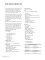
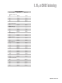
CS81 Series Standard Cell
▼
0.18µm CMOS Technology
Features
▼
•
•
•
•
•
•
•
•
•
•
•
•
•
•
•
0.13µm effective channel length
3 to 5 layers of metal interconnects
Very high density: 110K raw gates/mm2
Up to 28 million gates
Core power supply voltage: 1.8V to 1.1V
5 nW/gate/MHz power dissipation at 1.1V
11 ps gate delay at 1.8V and 1 fan-out
Junction temperature range: –40 to +125°C
I/Os: 3.3V, 2.5V, 1.8V, 5V tolerant
High-density diffused RAMs and ROMs
High-speed mixed-signal macros
Analog PLLs
Wide selection of advanced packaging options
Proven design methodology and tool support
Two cell libraries: high-performance and
high-density
CS81 I/O Interface Capabilities
1.8V Device
2.5V Device
3.3V Device
1.8V CMOS
2.5V CMOS
3.3V TTL
1.8V
CMOS
PLL
Clock Input
2.5V
CMOS
CS81
(1.8V)
T-LVTTL
P-CML
LVDS
SSTL
HSTL
High-Speed
Interface
High-Speed
Devices
Analog
Interface
3.3V
CMOS
PCI
AGP
USB
PCI Bus
AGP
USB Devices
ADC/DAC
Description
Fujitsu’s CS81, a 0.18µm (0.13µm Leff) standard-cell
product, is based on Fujitsu’s state-of-the-art CMOS
process technology, a deep sub-micron process designed
for today’s high-density and low-power SOC products.
The cell library, which is optimized for synthesis-based
designs, has accurate timing and power-characterized
data, cell areas, and statistical wire-load models. The
CS81 standard-cell library contains both high-performance and high-density cells, giving designers the
option of combining both types of standard cell blocks
on the same chip. The CS81 library supports popular
third-party tools and data-exchange file standards.
In addition to the traditional QFP packages, the CS81
family is available in TAB, EBGA, FBGA, and Flipchip BGA packages.
The CS81 chip cores can operate at 1.8V to 1.1V. The
I/Os, operating at 1.8V, 2.5V, 3.3V, or 5V tolerance, can
conveniently interface with various types of devices.
Interface options include low-swing, high-speed I/Os
and high-speed bus interface I/Os.
Design Methodology
Fujitsu’s design methodology ensures first-time silicon success by integrating proprietary point tools with popular,
sign-off-quality, industry-standard CAD tools such as:
Both inline and staggered I/O pad configurations are
available. Inline pads are available in both 70µm and
44µm pad pitch. The 70µm pads are wire bonded,
whereas the 44µm pads are used with TAB. The 66µm
wire-bond stagger pads can be used for optimizing the
die area of pad-limited designs.
CS81 offers a rich set of ADCs and DACs, PLLs, highspeed RAMs and ROMs, as well as a variety of other
embedded functions. The following blocks will be available in the near future:
• Special high-speed I/Os:
T-LVTTL, P-CML, LVDS, SSTL, and HSTL
• Special-purpose Interfaces:
PCI, AGP, and USB
• Logic design rule checker
• Delay calculator
• Quasi 3-D parasitic extraction tool
Fujitsu’s clock-driven design methodology is devised for low
power and low skew. The methodology identifies the bestsuited clock distribution strategy for a given design and
CS81 Series Standard Cell
predicts performance in advance. Fujitsu supports co-simulation, emulation and high-level floor-planning to optimize the power, timing, and size of the design. This
enables the designer to make effective architectural-level
decisions to achieve optimal design solutions.
Fujitsu’s design methodology supports cycle-based simulators and formal verification, as well as static timing analysis and the more conventional VHDL and Verilog simulators. Fujitsu’s design-for-test strategy includes boundary
scan (JTAG) and full and partial scan, as well as a built-in
self-test for memory.
Applications
CS81 offers high-density standard cells for very low-power
applications. Also provided in CS81 are high-performance
and area-optimized memories, mixed-signal blocks, analog functions, a rich set of IP Cores and Mega Macros,
and various I/O interfaces. The CS81 ASIC design kit,
combined with its supported EDA tool sets, is poised for
chip developments that require ease-of-tool use, proven
design flow and a quick time to market.
Mixed-Signal Macros
• A/D Converters
- 8-bit: 50 MS/s high-speed 3.3V
- 8-bit: 25 MS/s high-speed 3.3V
- 8-bit: 1 MS/s 3.3V
• D/A Converters
- 10-bit: 30 MS/s 3.3V
- 8-bit: 50 MS/s 3.3V
- 8-bit: 1 MS/s 3.3V
Multiplier Compiler
• Multiplicand (m): 4 ≤ m ≤ 32
• Multiplier (n): 4 ≤ n ≤ 32 (even numbers only)
Memory Macros
• SRAM Compiler: single and dual port (1RW/1R),
up to 72K bits per block
• High-speed SRAMs, up to 144K bits
• High-density SRAMs (1 RW)
512K ~ 1.1M bits (under development)
• Register files: 2R/2W
• ROM Compiler: up to 512K bits per block
Fujitsu Microelectronics, Inc.
Phase-Locked Loops
• Analog: up to 800 MHz
I/Os
• 1.8V, 2.5V, and 3.3V CMOS (2.5V is under
development)
• Slew-rate controlled
• Capable of driving large loads: 2, 4, 8, and 12 mA
sinking current
• Transceivers under development: P-CML, LVDS, PCI,
SSTL, and GTL
• AGP 2X and 4X
• 2.5 Gbps with clock recovery and
Serdes (under development)
• To be developed: 5V tolerant buffers
SOC IP Cores
• ARC 32-bit RISC
• 10/100 MAC
• 64/256 QAM
• MPEG2 Decoder/Demultiplexer
• 8VSB TV Demodulator
• AC3 Dolby Voice Decoder
• JPEG Encoder and Decoder
• PCI – 33/66 MHz, 32/64 bit cores
• USB Host Controller/Device
• I 2C
• IDE (ATA3) Host Controller
• Smart Card I/F
• IRDA I/R Interface
• To be developed:
- ARM 7TDMI Hard Macro
- Oak DSP Hard Macro
- More IPs are being added
ASIC Design Kit and EDA Support
Verilog Logic Simulators
from Cadence, Synopsys,
and Mentor
Verilog-XL, NC Verilog,
VCS, Model-sim (Verilog)
VHDL/VITAL Logic
Simulators from Synopsys,
Cadence, and Mentor
VSS, Model-sim (VHDL)
V-System, Leapfrog
Synthesis, DFT, and STA
tools from Synopsys
Design Compiler, Test
Compiler, and PrimeTime
Other EDA Tools
Chrysalis Design Verifyer
and Cadence DP
0.18µm CMOS Technology
No. of Pins/Balls
PACKAGE AVAILABILITY
Pin/Ball Pitch
Dimensions
TAB-BGA (Cavity-down)
304
352
480
560
660
720
0.8 mm
0.8 mm
1.0 mm
1.0 mm
1.0 mm
1.0 mm
21 mm
23 mm
31 mm
35 mm
40 mm
40 mm
1.27 mm
1.27 mm
40 mm
45 mm
0.50 mm
0.50 mm
0.40 mm
0.50 mm
28 mm
32 mm
28 mm
40 mm
0.50 mm
0.50 mm
14 mm
20 mm
0.50 mm
0.50 mm
0.50 mm
20 mm
24 mm
28 mm
0.80 mm
0.80 mm
0.80 mm
0.80 mm
0.80 mm
0.80 mm
0.50 mm
0.80 mm
0.75 mm
0.50 mm
0.80 mm
0.50 mm
10 mm
12 mm
12 mm
12 mm
14 mm
16 mm
10 mm
18 mm
18 mm
12 mm
18 mm
14 mm
1.27 mm
1.27 mm
1.27 mm
1.00 mm
1.00 mm
1.00 mm
42.4 mm
45.0 mm
47.5 mm
42.5 mm
45.0 mm
47.5 mm
EBGA (Cavity-down)
576
672
HQFP (Cavity-up)
208
240
256
304
TQFP (Cavity-up)
100
120
LQFP (Cavity-up)
144
176
208
FBGA (Cavity-up)
112
144
168
176
192
224
240
272
288
304
320
368
FC-BGA (Cavity-down)
1,089
1,225
1,369
1,681
1,849
2,116
Fujitsu Microelectronics, Inc.
FUJITSU MICROELECTRONICS AMERICA, INC.
Corporate Headquarters
1250 East Arques Avenue, Sunnyvale, California 94088-3470
Tel: (800) 866-8608 Fax: (408) 737-5999
E-mail: [email protected] Internet: http://www.fma.fujitsu.com
© 1999 Fujitsu Microelectronics, Inc.
All company and product names are trademarks or
registered trademarks of their respective owners.
Printed in the U.S.A. ASIC-FS-20820-10/99