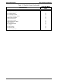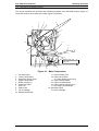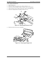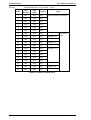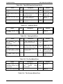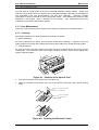
1
EPSON TERMINAL PRINTER EPL-5500 SERVICE MANUAL EPSON 4005431 - ii - NOTICE All rights reserved. Reproduction of any part of this manual in any form whatsoever without SEIKO EPSON’s express written permission is forbidden. The contents of this manual are subjects to change without notice. All efforts have been made to ensure the accuracy of the contents of this manual. However, should any errors be detected, SEIKO EPSON would greatly appreciate being informed of them. The above notwithstanding SEIKO EPSON can assume no responsibility for any errors in this manual or the consequence thereof. Epson is a registered trademark of Seiko Epson Corporation. General Notice: Other product names used herein are for identication purposes only and may be trademarks of their respective campanies. Copyright © 1995 by SEIKO EPSON CORPORATION Nagano, Japan -i- PRECAUTIONS Precautionary notations throughout the text are categorized relative to 1) personal injury and 2) damage to equipment. DANGER Signals a precaution which, if ignored, could result in serious or fatal personal injury. Great caution should be exercised in performing procedures preceded by DANGER Headings. WARNING Signals a precaution which, if ignored, could result in damage to equipment. The precautionary measures itemized below should always be observed when performing repair/ maintenance procedures. DANGER 1. ALWAYS DISCONNECT THE PRODUCT FROM BOTH THE POWER SOURCE AND PERIPHERAL DEVICES PERFORMING ANY MAINTENANCE OR REPAIR PROCEDURE. 2. NO WORK SHOULD BE PERFORMED ON THE UNIT BY PERSONS UNFAMILIAR WITH BASIC SAFETY MEASURES AS DICTATED FOR ALL ELECTRONICS TECHNICIANS IN THEIR LINE OF WORK. 3. WHEN PERFORMING TESTING AS DICTATED WITHIN THIS MANUAL, DO NOT CONNECT THE UNIT TO A POWER SOURCE UNTIL INSTRUCTED TO DO SO. WHEN THE POWER SUPPLY CABLE MUST BE CONNECTED, USE EXTREME CAUTION IN WORKING ON POWER SUPPLY AND OTHER ELECTRONIC COMPONENTS. WARNING 1. REPAIRS ON EPSON PRODUCT SHOULD BE PERFORMED ONLY BY AN EPSON CERTIFIED REPAIR TECHNICIAN. 2. MAKE CERTAIN THAT THE SOURCE VOLTAGE IS THE SAME AS THE RATED VOLTAGE, LISTED ON THE SERIAL NUMBER/RATING PLATE. IF THE EPSON PRODUCT HAS A PRIMARY AC RATING DIFFERENT FROM AVAILABLE POWER SOURCE, DO NOT CONNECT IT TO THE POWER SOURCE. 3. ALWAYS VERIFY THAT THE EPSON PRODUCT HAS BEEN DISCONNECTED FROM THE POWER SOURCE BEFORE REMOVING OR REPLACING PRINTED CIRCUIT BOARDS AND/OR INDIVIDUAL CHIPS. 4. IN ORDER TO PROTECT SENSITIVE MICROPROCESSORS AND CIRCUITRY, USE STATIC DISCHARGE EQUIPMENT, SUCH AS ANTI-STATIC WRIST STRAPS, WHEN ACCESSING INTERNAL COMPONENTS. 5. REPLACE MALFUNCTIONING COMPONENTS ONLY WITH THOSE COMPONENTS BY THE MANUFACTURE; INTRODUCTION OF SECOND-SOURCE ICs OR OTHER NONAPPROVED COMPONENTS MAY DAMAGE THE PRODUCT AND VOID ANY APPLICABLE EPSON WARRANTY. - ii - SAFETY INFORMATION This printer is a page printer which operates by means of a laser. There is no possibility of danger from the laser, provided the printer is operated according to the instructions in this manual provided. Since radiation emitted by the laser is completely confined within protective housings, the laser beam cannot escape from the machine during any phase of user operation. For United States Users; [Laser Safety] This printer is certified as a Class 1 Laser product under the U.S. Department of Health and Human Services (DHHS) Radiation Performance Standard according to the Radiation Control for Health and Safety Act of 1968. This means that the printer does not produce hazardous laser radiation. [CDRH Regulations] The Center for Devices and Radiological Health (CDRH) of the U.S. Food and Drug Administration implemented regulations for laser products on August 2, 1976. Compliance is mandatory for products marketed in the United States. The label shown below indicates compliance with the CDRH regulations and must be attached to laser products marketed in the United States. WARNING : Use of controls, adjustments or performance of procedures other than those specified in this manual may result in hazardous radiation exposure. [Internal Laser Radiation] Maximum Radiation Power: Wave Length: 5.0 × 10⁻⁴ (W) 790 ± 20 nm This is a Class IIIb Laser Diode Assay that has an invisible laser beam. The print head unit is NOT A FIELD SERVICE ITEM. Therefore, the print head unit should not be opened under any circumstances. For Other Countries Users; WARNING: Use of controls, adjustments or performance of procedures other than those specified in this manual may result in hazardous radiation exposure. This is a semiconductor laser. The maximum power of the laser diode is 5.0 × 10⁻⁴ W and the wavelength is 790 ± 20 nm. For Denmark Users; ADVARSEL Usynlig laserstråling ved åbning, når sikkerhedsafbrydere er ude af funktion. Undgå udsættelse for stråling. Klasse 1 laser produkt der opfylder IEC825 sikkerheds kravene. - iii - For Finland, Sweden Users; VAROITUS Laitteen käyttäminen muulla kuin tässä käyttöohjeessa mainitulla tavalla saattaa altistaa käyttäjän turvallisuusluokan 1 ylittävälle näkymättömälle lasersäteiylle. VARNING Om apparaten används på annat sätt än i denna bruksanvisning specificerats, kan användaren utsättas för osynlig laserstrålning, som överskrider gränsen för laser klass 1. For Finland, Sweden Service People VAROITUS Avattaessa ja suojalukitus ohitettaessa olet alttiina näkymättömälle lasersäteilylle. Älä katso säteeseen. VARNING Osynlig laserstrålning när denna del är öppnad och spärren är urkopplad. Betrakta ej strålen. For Norway Users; ADVARSEL Dersom apparatet brukes på annen måte enn spesifisert i denne bruksanvisning, kan brukeren utsettes for unsynlig laserstråling som overskrider grensen for laser klasse 1. Dette er en halvleder laser. Maksimal effeckt til laserdiode er 5.0 × 10⁻⁴ W og bølgelengde er 790 ± 20 nm. Laser Safety Labels [Label on rear printer case] A laser safety labels is attached on the outside of the printer shown below. For United State - iv - For Europe [Label inside printer] The following laser safety label will be attached inside the printer as shown below. For Denmark, Finland, Sweden, and Norway -v- PREFACE This manual describes functions, theory of electrical and mechanical operations, maintenance, and repair of EPL-5500. The instructions and procedures included herein are intended for the experience repair technician, and attention should be given to the precautions on the preceding page. The chapters are organized as follows: CHAPTER 1. GENERAL DESCRIPTION Provides a general product overview, lists specifications, and illustrates the main components of the printer. CHAPTER 2. OPERATING PRINCIPLES Describes the theory of printer operation. CHAPTER 3. DISASSEMBLY AND ASSEMBLY Includes a step-by-step guide for product disassembly and assembly. CHAPTER 4. ADJUSTMENTS Includes a step-by-step guide for adjustment. CHAPTER 5. TROUBLESHOOTING Provides Epson-approved techniques for adjustment. CHAPTER 6. MAINTENANCE Describes preventive maintenance techniques and lists lubricants and adhesives required to service the equipment. APPENDIX Describes connector pin assignments, circuit diagrams, circuit board component layout and exploded diagram. The contents of this manual are subject to change without notice. - vi - REVISION SHEET Revision Issue Date Revision Page Rev. A October 06, 1995 1st issue Revise the whole pages of the following chapters: Rev. B March 15, 1996 - vii - Chapter 1 Chapter 2 Chapter 3 Chapter 4 Chapter 5 Chapter 6 Chapter 1 General Description Table of Contents 1.1 FEATURES 1-1 1.2 SPECIFICATIONS 1-3 1.2.1 Basic Specification . . . . . . . . . . . . . . . . . . . . . . . . . . . . . . . . . . . . . . . . . . . 1-3 1.2.2 Electrical Specifications . . . . . . . . . . . . . . . . . . . . . . . . . . . . . . . . . . . . . . . 1-5 1.2.3 Reliability Specifications. . . . . . . . . . . . . . . . . . . . . . . . . . . . . . . . . . . . . . . 1-5 1.2.4 Environmental Conditions for Operating (Include Imaging Cartridge) . . . . 1-5 1.2.5 Environmental Conditions for Storage and Transportation . . . . . . . . . . . . 1-5 1.2.6 Applicable Standards . . . . . . . . . . . . . . . . . . . . . . . . . . . . . . . . . . . . . . . . . 1-6 1.2.7 Specifications for Consumable. . . . . . . . . . . . . . . . . . . . . . . . . . . . . . . . . . 1-6 1.2.8 Physical Specifications. . . . . . . . . . . . . . . . . . . . . . . . . . . . . . . . . . . . . . . . 1-6 1.2.9 Software Specifications . . . . . . . . . . . . . . . . . . . . . . . . . . . . . . . . . . . . . . . 1-7 1.3 INTERFACE SPECIFICATIONS 1-9 1.3.1 Parallel Interface. . . . . . . . . . . . . . . . . . . . . . . . . . . . . . . . . . . . . . . . . . . . . 1-9 1.3.1.1 Compatibility Mode of Parallel Interface . . . . . . . . . . . . . . . . . . . . 1-9 1.3.1.2 Reverse ModeMode Signal Timing . . . . . . . . . . . . . . . . . . . . . . . 1-11 1.3.2 Serial Interface . . . . . . . . . . . . . . . . . . . . . . . . . . . . . . . . . . . . . . . . . . . . 1-15 1.3.3 Optional LocalTalk Interface. . . . . . . . . . . . . . . . . . . . . . . . . . . . . . . . . . . 1-17 1.4 OPERATING INSTRUCTIONS 1.4.1 Control Panel . . . . . . . . . . . . . . . . . . . . . . . . . . . . . . . . . . . . . . . . . . . . . . 1.4.2 Printer Settings Functions . . . . . . . . . . . . . . . . . . . . . . . . . . . . . . . . . . . . 1.4.3 Service Mode . . . . . . . . . . . . . . . . . . . . . . . . . . . . . . . . . . . . . . . . . . . . . . 1.4.3.1 Heaxadecimal Dump Mode . . . . . . . . . . . . . . . . . . . . . . . . . . . . . 1.4.3.2 EEPROM Initialize Mode . . . . . . . . . . . . . . . . . . . . . . . . . . . . . . . 1.4.3.3 Factory Reset Mode . . . . . . . . . . . . . . . . . . . . . . . . . . . . . . . . . . 1.4.3.4 Default Setting Mode . . . . . . . . . . . . . . . . . . . . . . . . . . . . . . . . . . 1.4.4 Display of Messages . . . . . . . . . . . . . . . . . . . . . . . . . . . . . . . . . . . . . . . . 1.4.4.1 Status Messages . . . . . . . . . . . . . . . . . . . . . . . . . . . . . . . . . . . . . 1.4.4.2 Error Messages . . . . . . . . . . . . . . . . . . . . . . . . . . . . . . . . . . . . . . 1.4.4.3 Service Call Error Message . . . . . . . . . . . . . . . . . . . . . . . . . . . . . 1.4.5 Printer Sharing . . . . . . . . . . . . . . . . . . . . . . . . . . . . . . . . . . . . . . . . . . . . . 1.4.5.1 Port Fixed Mode . . . . . . . . . . . . . . . . . . . . . . . . . . . . . . . . . . . . . 1.4.5.2 Auto Sense Mode . . . . . . . . . . . . . . . . . . . . . . . . . . . . . . . . . . . . 1.4.6 Emulation Mode Switch Function . . . . . . . . . . . . . . . . . . . . . . . . . . . . . . . 1.4.6.1 Emulation Switch by SPL. . . . . . . . . . . . . . . . . . . . . . . . . . . . . . . 1.4.6.2 Intelligent Emulation Switch. . . . . . . . . . . . . . . . . . . . . . . . . . . . . 1.4.7 Bi Resolution Improvement Technology . . . . . . . . . . . . . . . . . . . . . . . . . 1.4.8 Toner Save Mode . . . . . . . . . . . . . . . . . . . . . . . . . . . . . . . . . . . . . . . . . . . 1.4.9 Optional Memory . . . . . . . . . . . . . . . . . . . . . . . . . . . . . . . . . . . . . . . . . . . 1-18 1-18 1-20 1-23 1-23 1-23 1-23 1-24 1-27 1-27 1-27 1-27 1-28 1-28 1-28 1-29 1-29 1-29 1-30 1-31 1-31 1.5 MAIN COMPONENTS 1.5.1 C169 MAIN-B Board. . . . . . . . . . . . . . . . . . . . . . . . . . . . . . . . . . . . . . . . . 1.5.2 PWB-E Board . . . . . . . . . . . . . . . . . . . . . . . . . . . . . . . . . . . . . . . . . . . . . . 1.5.3 PWB-F Board . . . . . . . . . . . . . . . . . . . . . . . . . . . . . . . . . . . . . . . . . . . . . . 1.5.4 Optical Unit . . . . . . . . . . . . . . . . . . . . . . . . . . . . . . . . . . . . . . . . . . . . . . . . 1.5.5 FUSING UNIT. . . . . . . . . . . . . . . . . . . . . . . . . . . . . . . . . . . . . . . . . . . . . . 1.5.6 Photoconductor Unit . . . . . . . . . . . . . . . . . . . . . . . . . . . . . . . . . . . . . . . . . 1-32 1-33 1-34 1-34 1-35 1-35 1-36 1.5.7 Developing Cartridge. . . . . . . . . . . . . . . . . . . . . . . . . . . . . . . . . . . . . . . . 1-36 1.5.8 Lower Paper Cassette Unit . . . . . . . . . . . . . . . . . . . . . . . . . . . . . . . . . . . 1-36 List of Figures Figure 1-1. Exterior View of the EPL-5500 . . . . . . . . . . . . . . . . . . . . . . . . . . . . . 1-1 Figure 1-2. Printable Area . . . . . . . . . . . . . . . . . . . . . . . . . . . . . . . . . . . . . . . . . . 1-4 Figure 1-3. Compatibility Mode Signal Timing . . . . . . . . . . . . . . . . . . . . . . . . . . 1-9 Figure 1-4. Parallel Interface State Switch Diagram . . . . . . . . . . . . . . . . . . . . . 1-12 Figure 1-5. Negotiation Timing Chart . . . . . . . . . . . . . . . . . . . . . . . . . . . . . . . . 1-13 Figure 1-6. Timing Chart of Data Transfer . . . . . . . . . . . . . . . . . . . . . . . . . . . . 1-13 Figure 1-7. Termination Timing Chart . . . . . . . . . . . . . . . . . . . . . . . . . . . . . . . . 1-14 Figure 1-8. Timing Chart of Interrupt . . . . . . . . . . . . . . . . . . . . . . . . . . . . . . . . . 1-14 Figure 1-9. Control Panel . . . . . . . . . . . . . . . . . . . . . . . . . . . . . . . . . . . . . . . . . 1-18 Figure 1-10. Port Fixed Mode . . . . . . . . . . . . . . . . . . . . . . . . . . . . . . . . . . . . . . 1-28 Figure 1-11. Auto Sense Mode . . . . . . . . . . . . . . . . . . . . . . . . . . . . . . . . . . . . . 1-28 Figure 1-12. Emulation Switch by SPL . . . . . . . . . . . . . . . . . . . . . . . . . . . . . . . 1-29 Figure 1-13. Intelligent Emulation Switch . . . . . . . . . . . . . . . . . . . . . . . . . . . . . 1-29 Figure 1-14. Effect of RITech . . . . . . . . . . . . . . . . . . . . . . . . . . . . . . . . . . . . . . 1-30 Figure 1-15. RITech Adjustment . . . . . . . . . . . . . . . . . . . . . . . . . . . . . . . . . . . . 1-30 Figure 1-16. Toner Save Mode . . . . . . . . . . . . . . . . . . . . . . . . . . . . . . . . . . . . . 1-31 Figure 1-17. Component Layout . . . . . . . . . . . . . . . . . . . . . . . . . . . . . . . . . . . . 1-32 Figure 1-18. C169 MAIN-B Board . . . . . . . . . . . . . . . . . . . . . . . . . . . . . . . . . . . 1-33 Figure 1-19. PWB-E Board . . . . . . . . . . . . . . . . . . . . . . . . . . . . . . . . . . . . . . . . 1-34 Figure 1-20. PWB-F Board . . . . . . . . . . . . . . . . . . . . . . . . . . . . . . . . . . . . . . . . 1-34 Figure 1-21. Optical Unit . . . . . . . . . . . . . . . . . . . . . . . . . . . . . . . . . . . . . . . . . . 1-35 Figure 1-22. Fusing Unit . . . . . . . . . . . . . . . . . . . . . . . . . . . . . . . . . . . . . . . . . . 1-35 Figure 1-23. Photoconductor Unit . . . . . . . . . . . . . . . . . . . . . . . . . . . . . . . . . . . 1-36 Figure 1-24. Developing Cartridge . . . . . . . . . . . . . . . . . . . . . . . . . . . . . . . . . . 1-36 List of Tables Table 1-1. Options for the EPL-5500. . . . . . . . . . . . . . . . . . . . . . . . . . . . . . . . . . 1-2 Table 1-2. Paper Feed Methods . . . . . . . . . . . . . . . . . . . . . . . . . . . . . . . . . . . . . 1-3 Table 1-3. Paper Types. . . . . . . . . . . . . . . . . . . . . . . . . . . . . . . . . . . . . . . . . . . . 1-3 Table 1-4. Usability of Special Papers . . . . . . . . . . . . . . . . . . . . . . . . . . . . . . . . 1-4 Table 1-5. Electrical Specifications . . . . . . . . . . . . . . . . . . . . . . . . . . . . . . . . . . . 1-5 Table 1-6. Differences between EPSON GL/2 and GL/2 in the HP LaserJet 4 Emulation. . . . . . . . . . . . . . . . . . . . . . . . . . . . . . . . . . . . . . . . . . . . . . . . . . . . . . . 1-7 Table 1-7. Built-in Fonts . . . . . . . . . . . . . . . . . . . . . . . . . . . . . . . . . . . . . . . . . . . 1-7 Table 1-8. Parallel Interface Pin Assignment . . . . . . . . . . . . . . . . . . . . . . . . . . 1-10 Table 1-9. Parallel Interface Pin Assignment . . . . . . . . . . . . . . . . . . . . . . . . . . 1-11 Table 1-10. Serial Interface Connector Pin Assignments . . . . . . . . . . . . . . . . . 1-15 Table 1-11. LocalTalk Connector Pin Assignments . . . . . . . . . . . . . . . . . . . . . 1-17 Table 1-12. Printer Settings. . . . . . . . . . . . . . . . . . . . . . . . . . . . . . . . . . . . . . . . 1-20 Table 1-13. Service MOde Select Timing . . . . . . . . . . . . . . . . . . . . . . . . . . . . . 1-23 Table 1-14. Default Settings Codes . . . . . . . . . . . . . . . . . . . . . . . . . . . . . . . . . 1-24 Table 1-15. Error Messages . . . . . . . . . . . . . . . . . . . . . . . . . . . . . . . . . . . . . . . 1-27 Table 1-16. Differences in Components for the C169 MAIN-B Board . . . . . . . 1-33 Rev. A 1-iii EPL-5500 Service Manual General Description 1.1 FEATURES The EPSON EPL-5500 is non-impact page printer that combines a semi-conductor laser with electrophotographic technology. This printer is small and light, and features high-speed, high-resolution printing. Maintenance is very easy as a result of various built-in diagnostic functions. The main features are: ❏ No ozone ❏ Printing speed — 6 ppm (pages per minute) ❏ Resolution — 600/300 dpi (dots per inch) ❏ Light weight — about 5 kg (11 lb) ❏ Small footprint ❏ Low running cost: separation of the development/toner cartridge and photoconductor unit ❏ HP LaserJet 4 emulation mode ❏ 22 built-in scalable fonts (8 Agfa and 14 TrueType fonts) ❏ High-performance controller (the controller’s CPU is a 22.5 MHz SPARKlite (MB86933H)) ❏ Bi Resolution Improvement Technology (BiRITech) refines the print quality by eliminating jagged edges from images and characters on 600 dpi and 300 dpi printing ❏ Memory Improvement Technology supported ❏ Optional EPSONScript Level 2 (PostScript compatible) module ❏ Optional WPS (Windows Printing System) ROM SIMM module ❏ Optional I239X, ESC/P 2 , and FX emulation ROM SIMM module ❏ EPSON Micro Gray Technology (EMGTech), which is available when using PCL and EPSONScript Level 2 mode, refines gray scale printing to be comparable to printing on a 1200-dpi printer ❏ Small and low-cost optional LocalTalk with serial interface module ❏ 1MB standard RAM and memory expansion available up to 32MB of RAM with the addition of optional SIMMs ❏ Bidirectional parallel interface ❏ Toner-saver mode supported ❏ A multi-user, multi-emulation mode ❏ IES (Intelligent Emulation Switch) allows switching between EPSONScript mode and another mode ❏ SPL (Shared Printer Language) enables switching of the printer mode by command Figure 1-1 shows an exterior view of the EPL-5500. Figure 1-1. Exterior View of the EPL-5500 Rev. B 1-1 General Description EPL-5500 Service Manual Table 1-1 lists the optional units available for the EPL-5500. Table 1-1. Options for the EPL-5500 Cat. No. Description C83218✽ Windows Printing System ROM SIMM — — C812491 Supports Windows Printing System EPSONScript Level 2 ROM SIMM Supports EPSONScript Level 2 mode (PostScript Level 2 compatible) fonts and commands (see Note 1) LQ/FX/I239X ROM SIMM Supports ESC/P 2, FX, 2390/2391 emulation modes NLSP Bitmap 2 font ROM Supports local NLSP bitmap fonts (see Note 2) NLSP Scalable font ROM Supports local NLSP scalable fonts (see Note 2) C83219✽ C83220✽ Note and IBM 250-sheet lower paper cassette for theLower paper cassette EPL-5500 (A4/B5) S050005 Developer cartridge Developer and toner cartridge S051029 Photoconductor unit — C82334✽ LocalTalk with serial I/F module (see Note 3) C83614✽ Interface cable RS-232C extension cable for C82334✽ C82335✽ Type-B EX box Type-B I/F card box (see Note 4) C82307✽/ 32 KB serial interface card C82308✽ C82310✽/ 32 KB parallel interface card C82311✽ (see Note 5) C82312✽ LocalTalk card (see Note 5) C82313✽ GPIB card (see Note 5) C82314✽ COAX interface card (see Note 5) C82315✽ TWINAX interface card (see Note 5) C82324✽ Ethernet interface card for NetWare (see Note 5) C82328✽ FAX card (see Note 5) C82331✽ Multi protocol Ethernet card (see Note 5) (see Note 5) Notes: 1. Requires added memory (RAM) over a total of 2 MB, including standard RAM. 2. NLSP font ROMs do not support ESC/P 2 and FX modes. 3. LocalTalk with serial I/F module (C82334✽) cannot be used with Type-B EX box (C82335✽). 4. Type-B EX box (C82335✽) cannot be used with LocalTalk with serial I/F module (C82334✽) . 5. Type-B EX box (C82335✽) must be installed while using the Type-B I/F card. 1-2 Rev. B EPL-5500 Service Manual General Description 1.2 SPECIFICATIONS This section provides statistical data for the EPL-5500. 1.2.1 Basic Specifications Printing method: Laser beam scanning and dry electrophotography Resolution: 600/300 dpi Printing speed: 6 ppm (letter/A4) First printing time (A4/LT): Less than 20 seconds (face-up output) Warm-up time: Less than 35 seconds (at rated current and 23° C (73° F) temperature) Paper supply: See Table 1-2. Table 1-2. Paper Feed Methods Capacity Using 20 lb. (75 g/m2) Paper Paper Supply Standard built-in paper tray Paper Size Usage Thickness (Ream Weight) 150 A5, B5, A4, LT,16 to 24 lb. GLT, EXE, LGL,(60 to 90 g/m2) GLG, F4, HL 5 to 10 Monarch, Envelopes made DL, C5, C6, of 20 to 24 lb. International B5, (75 to 90 g/m2) Commercial-10 paper Manual feed slot 1 Any size feedable (Note 2) 16 to 42 lb. (60 to 157 g/m2) Lower paper cassette (optional) 250 A4, B5 16 to 24 lb. (60 to 90 g/m2) Notes: 1. The weight in pounds (lb) is determined by the weight of 500 sheets cut to 17 × 22 inches; 1 g/m2 = 0.2659763 lb. 2. Paper size range: Paper types: width length 3 to 8.5 inches (76 to 216 mm) 5 to 14.0 inches (127 to 356 mm) See Table 1-3. Table 1-3. Paper Types Rev. B 1-3 General Description EPL-5500 Service Manual Standard paper Xerox 4024 DP paper 20 lb (75 g/m2) Normal paper Regular photocopier paper Bond paper Recycled paper 16 to 24 lb (60 to 90 g/m2) Special papers Card stock (90 to 157 g/m2) Envelopes Labels Letterhead Transparency (OHP) sheets Colored paper 4.0 mm Printable Area 4.0 mm 4.0 mm 4.0 mm Figure 1-2. Printable Area 1-4 Rev. B EPL-5500 Service Manual General Description Usability of special papers: See Table 1-4. Table 1-4. Usability of Special Papers Input OHP Envelopes Labels Card Stock Letterhead Standard built-in paper tray P P P P R Manual feed slot P P P P R Lower paper cassette N N N N P R: Reliable feeding and good image quality. P: Possible, but better avoided. N: Not supported. Paper feed alignment and direction: Center alignment for all sizes Paper ejection: Face down Output tray capacity: 100 sheets (face down) Printable area (standard paper): See Figure 1-2. Note: The actual printable area depends on the printer mode. Noise: Less than 35 dB(A), standby Less than 47 dB(A), operating Ozone density: Less than 0.01 ppm Toxicity: No toxicity exists in organic photoconductor (OPC), toner, or plastic materials Rev. B 1-5 General Description EPL-5500 Service Manual 1.2.2 Electrical Specifications Table 1-5. Electrical Requirements and Ranges Description Rated voltage Input voltage range 100 V Version 200 V Version 100 ∼ 120 VAC 220 ∼ 240 VAC 90 ∼ 132 VAC 198 ∼ 264 VAC Rated frequency range 50 ∼ 60 Hz Input frequency range 47 ∼ 63 Hz Power consumption Less than 500 W Power consumption while in standby mode Less than 600 W Less than 15 W (without option) 1.2.3 Reliability Specifications MPBF (Mean Prints Between Failures): Over 25,000 sheets Note: MPBF indicates average number of pages printed before occurrence of problem requiring replacement or service. MTBF (Mean Time Between Failures): Jam rate: Feed failure: Multiple paper feeds: Paper curl height: Leading edge bending (1 cm or more): MTTR (Mean Time To Repair): Durability: 3000 power on hours (POH) 1 out of 2,000 sheets or less (excluding multiple-sheet feeding) 1 out of 2,000 sheets or less (excluding multiple-sheet feeding) 1 out of 500 sheets or less 30 mm (1.2 inches) or less 1 out of 1,000 sheets 30 minutes or less 5 years or 180,000 sheets 1.2.4 Environmental Conditions for Operation (Including Imaging Cartridge) Temperature: 10 to 35° C (50 to 95° F) Humidity: 15 to 85% RH Altitude: 2,500 m (8,200 feet) or lower Levelness: 1° Illuminance: 3,000 lux or less (Must not be exposed to direct sunlight.) Surrounding space: Printer should have at least 100 mm of clearance on its sides and rear. 1.2.5 Environmental Conditions for Storage and Transportation Temperature: 0 to 35° C (32 to 95° F) Humidity: 30 to 85% RH Drop test: Clear to JIS Z0200-1987 Level 1 Vibration: Vibration frequency Acceleration Acceleration direction Resistance to atmospheric pressure: More than 61.3 KPa Storage life: 18 months (following date of manufacture) 1-6 5 to 100 Hz and 100 to 5 Hz 1G 3 direction Rev. B EPL-5500 Service Manual General Description 1.2.6 Applicable Standards Safety Standards 120 VAC model: 220/240 VAC model: UL 1950, CSA 22.2 No. 950 Deviation 3 EN 60950 (IEC950), NEMKO (IEC950), SETI (IEC950), SEMKO (IEC950), DEMKO (IEC950) Safety Regulations (Laser Radiation) 120 VAC model: 220/240 VAC model: FDA (NCDRH) Class 1 VDE 0837 (Laser Class 1) (IEC825), SETI (IEC825), SEMKO (IEC825), DEMKO (IEC825) EMI 120 VAC model: 220/240 VAC model: FCC Part 15 Subpart B Class B, DOC Class B Vfg 243 (VDE 0878 Part 3,30) EN55022 Class B (CISPR Pub.22 Class B) CE marking, EMC Others Toner: OPC: Ozone: Materials: No effect on human health (OSHA-TSCA, EINECS) No effect on human health (OSHA) Less than 0.01 mmp other UL478 (5th edition) SWISS environmental law (must contain no CdS) 1.2.7 Specifications for Consumables Life: Note: Developer and toner cartridge: 3,000 pages Photoconductor unit: 20,000 pages In continuous printing mode with A4/letter paper at a 5% image ratio (black/white ratio). The life varies, depending on the printing mode (continuous or intermittent) and/or the image ratio. Environmental Conditions for Storage and Transportation Temperature: 0 to 35° C (32 to 95° F) Humidity: 30 to 85% RH Drop test: Vibration: Resistance to atmospheric pressure: Storage term: Height 76 cm (30.4 inches) Same as printer More than 74 Kpa 18 months (following date of manufacture) 1.2.8 Physical Specifications Dimensions (Width × Depth × Height): Printer: Weight: Rev. B 352 × 264 × 299 mm (13.9 × 10.4 × 11.8 inches) Approx. 5 kg (11 lb), with consumables, excluding all options 1-7 EPL-5500 Service Manual General Description 1.2.9 Software Specifications HP LaserJet 4 emulation (PCL 5e) EPSON GL/2 mode (GL-like mode) EPSON GL/2 mode is similar to the GL/2 mode included in the HP LaserJet 4 emulation. Table 1-6 shows the differences between EPSON GL/2 mode and the LJ4 GL/2 mode. While in EPSON GL/2 mode, the operator can enter GL/2 mode without sending the ESC %#B (Enter GL/2 mode) command. If the operator’s application software cannot send the ESC %# B command, then use this mode. Built-in modes: Note: Table 1-6. Differences between EPSON GL/2 and GL/2 in the HP LaserJet 4 Emulation EPSON GL/2 Mode PCL mode Paper eject Auto eject Reduced printing Switch to PCL (ESC %#A) Reset (ESC E) Not available Supports PG, AF commands SelecType setting SelecType setting Not supported GL/2 for HP LaserJet 4 Emulation Mode Initial mode Supported in PCL Not available Available in PCL Supported Ejects paper and then initializes Ejects paper, switches to PCL, and then initializes Supported Supported Supported Not supported PJL, EJL, and ES Advance full page (PG, AF) The EPL-5500 GL/2 mode features all the commands of the LJ4-GL/2 mode, plus a few Note: additional commands. The GL/2 mode emulates some of the HP-GL plotter (HP 7475A, etc.) commands. If the application software uses unsupported commands for the GL/2 mode, print cannot be assured. Optional modes: EPSONScript Level 2 (PostScript Level 2 emulation) mode FX (FX-870/1170, LX-100) emulation mode ESC/P 2 (Stylus 800/1000) emulation mode WPS (Windows Printing System) mode Auxiliary software: Hex dump Status sheet Font sample Built-in fonts: See Table 1-7. Table 1-7. Built-in Fonts Resident Fonts Bitmap fonts Line Printer16.66 cpi(Portrait) Scalable fonts Dutch 801Roman SWC Dutch 801Bold SWC Dutch 801Italic SWC Dutch 801Bold Italic SWC Swiss 742SWC Swiss 742Bold SWC Swiss 742Medium Italic SWC S: Supported, NS: Not Supported Rev. B Applicable Mode HP LJ4, GL/2 S S S S S S S S 1-7 General Description EPL-5500 Service Manual Table 1-7. Built-in Fonts (Continued) Resident Fonts Scalable fonts Swiss 742Bold Italic SWC Swiss 721Roman SWM Swiss 721Bold SWM Swiss 721Oblique SWM Swiss 721Bold Oblique SWM Dutch 801Roman SWM Dutch 801Bold SWM Dutch 801Italic SWM Dutch 801Bold Italic SWM Symbol SetSWA More WingBatsSWM CourierSWC CourierBold SWC CourierItalic SWC CourierBold Italic SWC S: Supported, NS: Not Supported 1-8 Applicable Mode HP LJ4 GL/2 S S S S S S S S S S S S S S S Rev. B EPL-5500 Service Manual General Description 1.3 INTERFACE SPECIFICATIONS The EPL-5500 is equipped with the following external interfaces: ❏ Parallel interface ❏ Optional LocalTalk/serial interface ❏ Optional Type B interface with Type-B EX box 1.3.1 Parallel Interface The parallel interface has the following two modes: ❏ Compatibility mode (same as parallel interface for EPSON’s current page printer) ❏ Reverse mode 1.3.1.1 Parallel Interface Compatibility Mode System: Handshaking: Connector type: Applicable plug: Transfer speed: Signal timing: Signal description: STROBE synchronization, 8-bit parallel data transfer BUSY and ACKNLG signals P90-25027-1 (Amphenol) receptacle 57-30360 (Amphenol or equivalent) Approximately 400,000 bytes/second (max.) See Figure 1-3. See Table 1-8. 0.5 µ s 0.5 µ s (minimum) (minimum) DATA 1-8 VALID VALID 0.5 µ s (minimum) STR OBE 0.5 µ s (maximum) BU SY 0s 0.5 or 5 µ s (min.) (minimum) AC KN LG 1 or 10 µ s (typical) Figure 1-3. Compatibility Mode Signal Timing Rev. B 1-9 General Description EPL-5500 Service Manual Table 1-8. Parallel Interface Pin Assignments Pin No. Signal Name STROBE I/O IN 1 DATA 1-8 2-9 IN Description STROBE is a strobe pulse used to read data from the host computer. The pulse width must be more than 0.5 µsec. Normally it is HIGH, and data is latched at the trailing edge of this signal. DATA 1 to 8 are parallel data bits. When the signal is HIGH, the data bit is 1, and when it is LOW, the data bit is 0. The most significant bit (MSB) is DATA 8. The signal state must be maintained for 0.5 µsec. on either side of the STROBE signal active edge. ACKNLG ACKNLG is an acknowledge pulse with an approximate width OUT of 1 or 10 µsec. This signal goes LOW when the data reception is completed, which indicates that the printer can accept new data. Timing with the BUSY signal is specified through SelecType. BUSY OUT The BUSY signal informs the host computer of the printer state. When the signal is HIGH, the printer cannot accept data. PE The PE signal indicates paper empty for the standard tray OUT selected through SelecType or command, or for the optional paper cassette. Paper empty is indicated by HIGH. 13 SLCT OUT Used in reverse mode. 14 AUTO-FEED IN Not used. 15 NC — Not used. 16 GND — Logic ground level. 17 CHASSIS GND — Connected to the printer chassis. The printer chassis GND and the signal GND are connected to each other. 18 NC — Not connected. 19-30 GND — Ground level for the twisted pair return signal. INIT IN The STROBE signal is ignored when this signal is LOW. 10 11 12 31 ERROR 32 This level goes LOW when the printer is: • Out of paper OUT • Paper jam • In the error state • Off line 33 GND — Same as for pins 19 to 30. 34 NC — Not used. 35 +5 — Pulled up to +5 V through 1.0K-ohm resistance. 36 SLCT IN — Used in reverse mode. 1-10 Rev. B EPL-5500 Service Manual General Description 1.3.1.2 Reverse Mode Reverse mode for the EPL-5500 supports the IEEE-P1284 nibble mode. This printer can run in reverse mode, in which the printer can inform the computer of its status with EJL and PJL commands. System: IEEE-P1284 nibble mode Connector type: P90-25027-1 (Amphenol) receptacle Applicable plug: 57-30360 (Amphenol or equivalent) Signal description: See Table 1-9. Table 1-9. Parallel Interface Pin Assignment Pin No. 1 Signal Name STROBE I/O IN DATA 1-8 2-9 IN Description HostClk: This signal is a strobe pulse used to read extension request values from the host computer during negotiation. These signals are data bits of extension request values received during negotiation. This printer supports following values: 0000 0100: Request Device ID (sent in nibble mode) 0000 0000: Request nibble mode 10 ACKNLG OUT PtrClk: Printer sends clock data. 11 BUSY OUT PtrBusy: Printer sends data bits 3 and 7 during data transfer to host computer. PE OUT AckDataReq: Printer sends data bits 2 and 6 during data transfer to host computer. SLCT OUT Xflag: Printer sends data bits 2 and 6 during data transfer to host computer. 12 13 AUTO-FEED 14 IN HostBusy: This signal informs the printer of the host computer’s state. When the signal is HIGH, the host computer cannot accept data. 15 NC — Not used. 16 GND — Logic ground level. 17 CHASSIS GND — Connected to the printer chassis. The printer chassis GND and the signal GND are connected to each other. 18 NC — Not connected. — Ground level for the twisted pair return signal. IN nInit: Fixed at HIGH level. 19-30 GND 31 INIT 32 ERROR 33 GND — Same as for pins 19 to 30. 34 NC — Not used. 35 +5 — Pulled up to +5 V through 1.0K-ohm resistance. 36 SLCT IN IN 1284Active: If this signal is set to HIGH, this printer is actively in P1284 (reverse mode). Rev. B OUT nDataAvail: Printer sending data bits 0 and 4 during data transfer to host computer. 1-11 General Description EPL-5500 Service Manual Compatibility M ode Forward D ata Transfer S TROB E ACK and BUSY Forward Idle SLCT IN=HIGH ERR=HI GH No data sent Terminate Failed Negotiation Negotiation SLCT I N=LOW E RR=L O W Sending data E RR = L O W Sending data Host Busy Data Not Available ERR=HI GH No data sent Reverse Dat a Transfer A UT O FEED=LOW Reverse Idle A UT O FE ED=L OW Request to send data Host Busy Dat a Available A UT O FEED=HIG H ERR= LO W Interrupt Ho st Figure 1-4. Parallel Interface State Switch Diagram Figure 1-4 shows the switch diagram for the parallel interface state. 1-12 Rev. B EPL-5500 Service Manual General Description Figure 1-5 shows the negotiation timing chart. DATA 00h or 04h SEL-IN STROBE AUTO-FEED ACKNLG BUSY PE Peripheral Busy Status Current Peripheral Status Note1 SLCT ERROR Note 2 Current Peripheral Status Note1 Compatibility Negotiation HB DA or HB DNA (Note 3) Idle or Transfer Figure 1-5. Negotiation Timing Chart Notes: 1. This signal is set to HIGH when no data is being sent. This signal is set to LOW during sending of data. 2. This signal is set to HIGH if the extension request value was 04h. 3. HB DA: Host Busy Data is Available HB DNA: Host Busy Data is Not Available Figure 1-6 shows the data transfer timing chart. Notes: DATA SEL-IN STROBE AUTO-FEED ACKNLG BUSY Peripheral Busy Status Bit 3 Bit 7 PE Bit 2 Bit 6 Note 1 SLCT Bit 1 Bit 5 Note 2 ERROR Bit 0 Bit 4 Note 1 HB DA Peripheral Busy Status Negotiation Idle or Transfer HB DA or HB DNA (Note 3) Figure 1-6. Timing Chart for Data Transfer 1. 2. 3. This signal is set to HIGH when no data is being sent. This signal is set to LOW during sending of data. This signal is set to HIGH, if extension request value was 04h. HB DA: Host Busy Data is Available HB DNA: Host Busy Data is Not Available Rev. B 1-13 General Description EPL-5500 Service Manual Figure 1-7 shows the timing chart for termination. DATA SEL-IN STROBE AUTO-FEED Note 3 ACKNLG BUSY Peripheral Busy Status PE Note 1 SLCT Note 2 ERROR Note 1 HB DNA, Idle, or HB DA Peripheral Busy Status Current Peripheral Status Current Peripheral Status Termination Compatibility Figure 1-7. Termination Timing Chart Notes: 1. The signal is HIGH when HB DNA. The signal is LOW when HB DA. 2. The signal is set to HIGH, if the extension request value was 04h. 3. Idle = LOW. Figure 1-8 shows the timing chart for interrupts. DATA SEL-IN STROBE AUTO-FEED ACKNLG BUSY Peripheral Busy Status PE Note 1 SLCT ERROR Reverse Idle Interrupt HB DA Transfer Figure 1-8. Timing Chart for Interrupts Note: 1-14 The signal is set to HIGH, if the extension request value was 04h. Rev. B EPL-5500 Service Manual General Description 1.3.2 Serial Interface This printer can use the optional LocalTalk/serial interface module. Type: RS-232C/current loop Transfer system: Full duplex Synchronization: Asynchronous start-stop system Start-bit: 1 bit Stop-bit: 1 or 2 bits Data length: 7 bits or 8 bits Parity: Odd, even, or none Protocol: X-ON/X-OFF (can be combined with DTR control) DTR control (can be combined with X-ON/X-OFF) Transfer speed: 300, 600, 1200, 2400, 4800, 9600, 19200, 38400, or 57600 bps Error: Overrun error: Processed as missing data and replaced by “*” Parity error: Replaced by “*” Framing error: Replaced by “*” Breaking character: Ignored Signal description: See Table 1-10. Table 1-10. Serial Interface Pin Assignments Pin No. 1 Signal Name CHASSIS-GND TXD 2 I/O — Description Connected to the printer chassis. The printer chassis GND and signal GND are connected to each other. Serial ASCII data output by the printer. It maintains the OUT “MARK” state (LOW level) between transmitted character codes. Logic 0 is at HIGH level (SPACE) and logic 1 is at LOW level (MARK). 3 RXD IN Serial ASCII data input to the printer. It maintains “MARK” state (LOW level) between received character codes. 5 CTS IN Always ignored. 7 SIGNAL-GND — Ground. TTY-TXD Current loop signal: HIGH impedance (SPACE) between pins 17 and 24 or X-ON signal sent across pins 17 and 24 indicates OUT that the printer is ready to accept data; LOW impedance (MARK) or X-OFF signal being sent indicates that the printer is busy. DTR Signal output by printer. When the DTR signal is HIGH, the printer can receive the RXD signal. The SelecType settings do not specify DTR control, the signal level is HIGH while printer OUT power is on. When the SelecType setting is used for DTR control, DTR goes LOW in case of any error conditions. The data (RXD) from host computer must be stopped within 128 characters after DTR goes LOW. 17 20 23 TTY-RXD Return — Current loop signal: Current return for pin 17 24 TTY-TXD Return — Current loop signal: Input data current loop 25 TTY-RXD IN Current loop signal: Current return for pin 25 Note : Rev. B The DTR state can be selected through printer settings. 1-15 General Description EPL-5500 Service Manual Handshaking When the vacant area for data in the input buffer drops to 256 bytes, the printer outputs an X-OFF code or sets the DTR signal level to LOW, indicating that the printer cannot receive more data. Once the vacant area for data in the buffer recovers to 512 bytes, the printer outputs an X-ON code or sets the DTR flag to HIGH, indicating that the printer is again ready to receive data. Protocol There are two types of protocols, as listed below, and each of them can be designated by SelecType independently. ❏ DTR/DSR protocol SelecType is used to execute the DTR/DSR control protocol. The DTR signal is set to HIGH when the printer is ready to receive data, and to LOW when conditions indicate an error or that the receiving buffer is full. When the error is cleared and the printer returns to on-line mode, the signal returns to HIGH. When SelecType is used to set the DTR control OFF, DTR is always set to HIGH. The printer transmits TXD only when DSR is at the HIGH level (DSR is always considered HIGH when the SelecType setting for DSR is OFF). X-ON/X-OFF transmission is independent of the DSR state. ❏ X-ON/X-OFF (DC1/DC3) protocol SelecType is used to execute the X-ON/X-OFF protocol. The X-OFF (DC3) code is output if status indicates an error, and the printer warns the host to stop data transmission within 256 characters. No further X-OFF codes are sent in response to additional data received from the host after the X-OFF code has been sent once. The X-ON (DC1) code is output after all conditions given in the error are cleared. When the remaining capacity of the receive buffer reaches 512 characters, X-OFF (DC3) is output once. It is sent only once, even if there are multiple errors. The printer goes on line automatically at power on, and outputs an X-ON code. Transmission of X-ON/X-OFF codes can be defined by SelecType. 1-16 Rev. B EPL-5500 Service Manual General Description 1.3.3 Optional LocalTalk Interface This printer can use the optional LocalTalk/ serial interface module. Type: LocalTalk Signal level: Same as RS-422 signal level Protocol: X-ON/X-OFF (cannot be combined with DTR control) DTR control (cannot be combined with X-ON/X-OFF) Transfer speed: 230.4K bps Signal description: See Table 1-11. Table 1-11. LocalTalk Interface Pin Assignments Pin No. 1 Signal Name DTR 2 CTS TXD- 3 4 GND I/O Description Signal output by the printer. When the DTR signal is HIGH, the OUT printer can receive the RXD signal. IN Serial ASCII data output from the printer. HIGH level; when SD+ voltage is higher than the SD- voltage. OUT LOW level; when SD+ voltage is less than the SD- voltage. Logic 0 is SPACE and logic 1 is MARK. The state must be maintained between transmitted character codes. — Ground. IN Serial ASCII data input from computer. HIGH level; when RD+ voltage is higher than RD- voltage. LOW level; when RD+ voltage is less than RD- voltage. Logic 0 is “SPACE” and logic 1 is “MARK” state must be maintained between transmitted character codes. RXD5 The printer transmits the data through TXD while CTS is HIGH. 6 TXD+ 7 NC — No connect. 8 RXD+ IN Refer to RXD-. Rev. B OUT Refer to TXD-. 1-17 General Description EPL-5500 Service Manual 1.4 OPERATING INSTRUCTIONS This section describes functions performed through the control panel, such as printing a status sheet, hexadecimal dump, and printer settings functions. 1.4.1 Control Panel The printer control panel gives you easy control over most common printer operations. The panel consists of indicator lights and a button. LED (Yellow) LED (Red) Button Figure 1-9. Control Panel Indicator lights ❏ Yellow light ON: Communication with the host is possible. Fast flashing: Receiving data or warming up. Slow flashing: Received data is stored in the printer but has not been printed. OFF: Printer is power off. ❏ Red light ON: Paper jam or cover open. Fast flashing: Feed jam, paper empty. Slow flashing: One of these errors: SOFT ERROR, PRINT OVERRUN, MEMORY OVERFLOW, CHECK PAPER SIZE, IMAGE OPTIMUM OFF: No error condition. 1-18 Rev. B EPL-5500 Service Manual General Description Functions of Pressing the Button ❏ While the Red light flashes slowly: Function of button Operation Clears an error. Hold down the button until the yellow and Red lights both go on after release. The printer prints a status sheet indicating the error type. ❏ While the Red light flashes fast: Function of button Prints any of the following page. - Feed jam or paper empty page - Manual feed page Operation Load the paper or clear the jam, and then hold down the button until the yellow and Red lights go on, then release to continue printing. ❏ While yellow light is flashing slowly (except in EPSONScript mode): Function of button Prints out data in the printer’s memory. Operation Hold down the button until the yellow and red lights go on, then release the button to continue printing. ❏ While the yellow light is on (except in WPS mode): Function of button Prints a status sheet. Operation Hold down the button until the yellow and red lights go on, then release the button to continue printing. The yellow light flash while the status sheet is being printed. ❏ Reset (always effective except during warm up or status sheet printing): Function of button Clears current port. Operation Hold down the button until the yellow and red lights go on, and when these lights start flashing alternately, release the button. ❏ Warm boot (always effective except during warm up or status sheet printing): Function of button Warm boot (same as power on reset, except for engine initialization). Operation Hold down the button until the yellow and red lights start flashing at the same time, then release the button. Rev. B 1-19 General Description EPL-5500 Service Manual 1.4.2 Printer Settings Functions The printer settings function from the Remote Control Panel (software) lets the user control most of the printer’s functions, such as printing test pages, selecting a paper size, and changing the printer’s configuration. Table 1-12 shows the printer settings options. Table 1-12. Printer Settings Menu PRINTING LJ4 PS* ESCP2* Item Available Options COPIES 1 to 999 PAGE SIZE A4, A5, B5, LT, HLT, LGL, GLT, GLG, EXE, F4, MON, C10, DL, C5, IB5, CTM ORIENTATION PORT, LAND MANUAL FEED OFF, ON RITech OFF, LIGHT, MEDIUM, DARK TONER SAVE OFF, ON FONT SRC RESIDENT, SIMM, DOWNLOAD FONT NUMBER 0 to (available) PITCH 0.44 to 99.99 CPI (0.01 steps) HEIGHT 4.00 to 999.75 PT. (0.25 steps) SYMSET Roman-8, ECM94-1, 8859-2 ISO, 8859-2 ISO, IBM-US, IBM-DN, PcMultiling, PcE.Europe, PcTk437, WiAnsi, WiE.Europe, WiTurkish, DeskTop, PsText, VeInternati, VeUS, MsPublishin, Math-8, PsMath, VeMath, PiFont, Legal, UK, ANSI ASCII, Swedis2, Italian, Spanish, German, Norweg1, French2, Windows FORM 5 to 128 lines SRC SYMSET* 0 to 3199 DEST SYMSET* 0 to 3199 ERR SHEET OFF, ON MicroGray OFF, ON PROTECT LEVEL 1 to 5 Font Courier, Roman, Sans serif, Roman-T, Sans-H, Script Pitch 10 CPI, 12 CPI, 15 CPI, Prop Condensed OFF, ON T-Margin 0.40 to 1.50 Inch (0.05 steps) Text 1 to (available) lines CG Table Pc USA, Italic, PcMultilin, PcPortuguese, PcCanFrenc, PcNordic, PcTurk2, Pc.E.Europe, BpBRASCII, BpAbicomp Country USA, France, Germany, UK, Denmak, Sweden, Italy, Spain1, Japan, Norway, Denmark2, Spain2, LatinAmeric, Korea, Legal * With option Table 1-12. Printer Settings (Continued) Menu 1-20 Item Available Options Rev. B EPL-5500 Service Manual ESCP2 * (Continued) FX* I239X* General Description Auto CR ON, OFF Auto LF OFF, ON Bit Image Dark, Light, BarCode Zero Char 0, φ Font Courier, Prestige, Roman, Sans serif, Script Pitch 10 CPI, 12 CPI, 15 CPI, Prop Condensed OFF, ON T-Margin 0.40 to 1.50 Inch (0.05 steps) Text 1 to (available) lines CG Table Pc USA, Italic, PcMultilin, PcPortuguese, PcCanFrenc, PcNordic, PcTurk2, Pc.E.Europe, BpBRASCII, BpAbicomp Country USA, France, Germany, UK, Denmak, Sweden, Italy, Spain1, Japan, Norway, Denmark2, Spain2, LatinAmerica Auto CR ON, OFF Auto LF OFF, ON Bit Image Dark, Light, BarCode Zero Char 0, φ Font Courier, Prestige, Gothic, Orator Script, Presentor Pitch 10 CPI, 12 CPI, 15 CPI, 17 CPI, 20 CPI, 24 CPI, Prop Code Page 437, 850, 860, 863, 865 T-Margin 0.40 to 1.50 Inch (0.05 steps) Text 1 to (available) lines Auto CR OFF, ON Auto LF OFF, ON Alt.Graphics OFF, ON Bit Image Dark, Light, BarCode Zero Char 0, φ * With option Rev. B 1-21 General Description EPL-5500 Service Manual Table 1-12. Printer Settings (Continued) Menu JOB EMULATION CONFIG PARALLEL SERIAL TEST Item Available Options PAGE PROTECT AUTO, ON RESOLUTION 600, 300 IMAGE OPTIMUM AUTO, OFF, ON TIMEOUT 5 to 300 PARALLEL LJ4, ESCP2*, FX*, I239X*, PS*, GL2, AUTO* SERIAL* LJ4, ESCP2*, FX*, I239X*, PS*, GL2, AUTO* L/T* LJ4, ESCP2*, FX*, I239X*, PS*, GL2, AUTO* AUX* LJ4, ESCP2*, FX*, I239X*, PS*, GL2, AUTO* AUTO CONT OFF, ON STANDBY ENABLE, DISABLE DENSITY 3, 4, 5, 1, 2 INTERFACE AUTO, PARALLEL, SERIAL*, L/T*, AUX* TOP OFFSET 0 to 99 LEFT OFFSET 0 to 99 PAGE COUNT 0 to 262143 SPEED FAST, LOW BI-D ON, OFF WORD LENGTH 8, 7 BAUD RATE 9600, 19200, 38400, 57600, 300, 600, 1200, 2400, 4800 PARITY NONE, EVEN, ODD STOP BIT 1, 2 DTR ON, OFF XON/XOFF ON, OFF STATUS SHEET — PS STATUS SHEET* — PS FONT SAMPLE* — PS FACT SHEET* — EXT PRINTER INFO — * With option 1-22 Rev. B EPL-5500 Service Manual General Description 1.4.3 Service Mode This printer has the following four service modes: ❏ Hexadecimal dump mode ❏ EEPROM format mode ❏ Factory reset mode ❏ Default setting mode Each service mode can be activatted selectively, by turning the printer on while hold down the button and release it at the corresponding timing shown in table below. Table 1-13. Service Mode Select Timing Order Pattern LED (Yellow) LED (Red) Mode 1 Pattern 0-0 ON ON NA 2 Pattern 0-1 OFF OFF NA 3 Pattern 1 ON OFF Hexadecimal dump mode 4 Pattern 2 OFF ON EEPROM Initialize mode 5 Pattern 3 ON OFF Factory reset mode 6 Pattern 4 OFF OFF Default setting mode *1 *1: Can be performed by the user. 1.4.3.1 Hexadecimal Dump Mode Hexadecimal dump mode is a useful tool in troubleshooting data control problems. To enter hexadecimal dump mode, release the button at the mode select timing "Pattern-1". To quit the hexadecimal dump mode, turn off the printer or perform the warm-boot operation. 1.4.3.2 EEPROM Initialize Mode EEPROM initialize operations are required only when the main board or EEPROM is replaced and these operations are specified in the accompanying documentation. This mode resets all user settings to the factory default settings and clears the printer status information (page counter and jam counter). To perform EEPROM initialize mode, release the button at the mode select timing "Pattern-2" and press the bottun again within 2 seconds from the release. The LED lights flashes alternately during the initialization. If the button is not pressed within 2 seconds after release, the printer enters nomal state without initialize operation. 1.4.3.3 Factory Reset Mode The factory reset mode resets the printer settings to the factory default settings (the page counter and jam counter are not cleared). To enter factory reset mode, release the button at the mode select timing "Pattern-3" and press the button again within 2 seconds after release. The LED lights flashes alternately during the reset operation. If the button is not pressed within 2 seconds after release, the printer enters the nomal state without reset operation. Rev. B 1-23 General Description EPL-5500 Service Manual 1.4.3.4 Default Settings The default settings function is used to enter printer settings. The procedure for entering default settings is: 1. To enter the default settings mode, turn on the printer while holding down the button until yellow and red lights turn off and on and off. 2. Press the button the number of times for the 1st code, while the yellow light is flashing. 3. Press the button the number of times for the 2nd code, while the red light is flashing. 4. Press the button the number of times for the 3rd code, while all lights flash. 5. If you need end the default settings mode, return step 2 and input the "111" code. If you need set the other settings, return to step 2. Thable 1-14 shows default settings codes. Table 1-14. Default Settings Codes Menu Item Available Options End of default settings mode PARALLEL SPEED Bi-D SERIAL* WORD LENGTH BAUD RATE PARITY STOP BIT DTR XON/XOFF Default Settings Codes 1st 2nd 3rd Code Code Code 1 1 1 FAST 1 1 2 SLOW 1 1 3 ON 1 1 4 OFF 1 1 5 8 1 2 1 7 1 2 2 9600 1 2 3 19200 1 2 4 38400 1 2 5 27600 1 3 1 300 1 3 2 600 1 3 3 1200 1 3 4 2400 1 3 5 4800 1 4 1 NONE 1 4 2 EVEN 1 4 3 ODD 1 4 4 1 1 4 5 2 1 5 1 ON 1 5 2 OFF 1 5 3 ON 1 5 4 OFF 1 5 5 * With option Table 1-14. Default Settings Code (Continued) Menu 1-24 Item Available Options Default Settings Codes 1st 2nd 3rd Code Code Code Rev. B EPL-5500 Service Manual EMULATION PARALLEL SERIAL* General Description LJ4 2 1 1 ESCP2* 2 1 2 FX* 2 1 3 I239X* 2 1 4 PS* 2 1 5 GL2 2 2 1 AUTO* 2 2 2 LJ4 2 3 2 ESC/P2* 2 3 3 FX* 2 3 4 I239X* 2 3 5 PS* 2 4 1 GL/2 2 4 2 AUTO* 2 4 3 LT* AUX* SERIAL* LT* AUX* SERIAL* LT* AUX* SERIAL* LT* AUX* SERIAL* LT* AUX* SERIAL* LT* AUX* SERIAL* LT* AUX* * With option Rev. B 1-25 General Description EPL-5500 Service Manual Table 1-14. Default Settings Code (Continued) Menu ESC/P2* / FX* STATUS SHEET PRINTING Item CG Table LANGUAGE PAGE SIZE ORIENTATION MANUAL FEED TONER SAVER JOB CONFIG RESOLUTION AUTO CONT STANDBY INTERFACE Available Options PcUSA Deafult Settings Codes 1st 2nd 3rd Code Code Code 2 5 3 Italic 2 5 4 PcMultilin 2 5 5 PcPortugue 3 1 1 PcCanFrenc 3 1 2 PcNordic 3 1 3 PcTurkish 3 1 4 PcE.Europe 3 1 5 BpBRASCII 3 2 1 BpAbicomp 3 2 2 ENGLISH 3 2 3 FRENCH 3 2 4 GERMAN 3 2 5 ITALIAN 3 3 1 SPANISH 3 3 2 A4 3 5 1 LT 3 5 2 LGL 3 5 3 CTM 3 5 4 PORT 3 5 5 LAND 4 1 1 OFF 4 1 2 ON 4 1 3 OFF 4 1 4 ON 4 1 5 600 4 2 1 300 4 2 2 OFF 4 2 3 ON 4 2 4 ENABLE 4 2 5 DISABLE 4 3 1 AUTO 4 3 2 PARALLEL 4 3 3 SERIAL 4 3 4 LT 4 3 5 AUX 4 4 1 * With option 1-26 Rev. B EPL-5500 Service Manual General Description 1.4.4 Display of Messages This printer indicates three types of messages with the LED lights or status sheet: status messages, error messages, and the service call error message. 1.4.4.1 Status Messages The LED lights normally indicate the printer’s status. (Refer to Section 1.4.1.) 1.4.4.2 Error Messages If any of the following errors occurs, it will be printed on the status sheet (Refer to Section 1.4.2.). Clear the error immediately using the measures shown in the following table. Table 1-15. Error Messages Message SOFT ERROR PAPER JAM PRINTER OPEN MANUAL FEED PAPER SET PRINT OVERRUN MEM OVERFLOW CHECK PAPER SIZE IMAGE OPTIMUM Status Measures Printer detected a CPU error or soft— error. (Refer to Chapter 5.) A paper jam has occurred. Open the cover and remove the jammed paper. Then close the cover. Cover is open. Close the cover. Select manual feed and beginInsert paper and press button. printing data. No paper is left in either the Load paper in paper tray or optional standard tray or the optionalcassette and press button. cassette. Engine speed faster than print imagePress the button. processing. Data has filled the buffer. Confirm and press the button. And add optional SIMM. The paper size in the tray is differentChange the paper and print again. from the paper size chosen. The printer uses a lower printErase downloaded data or add a quality. SIMM. 1.4.4.3 Service Call Error Message The LED lights flash randomly, when the printer detects a service call error. (Refer to Chapter 5.). Rev. B 1-27 General Description EPL-5500 Service Manual 1.4.5 Printer Sharing This section describes printer sharing. This printer has two methods of printer sharing, port fixed mode and auto sense mode. These modes are selected by “INTERFACE” in the printer settings menu. 1.4.5.1 Port Fixed Mode When the printer is in port fixed mode, only one interface port is active. Data from other ports is ignored. 1.4.5.2 Auto Sense Mode M ode Ass ignment HP m ode ESC/ P2 m ode User 1 F X m ode Par allel GL2 m ode EPSONScr ipt m od e Switched by printer settings Input buffer M ode Ass ignment Memory HP m o d e ESC/ P2 m ode User 2 L/T or Serial or AUX F X m ode GL2 m ode EPSONScr ipt m od e Figure 1-10. Port Fixed Mode It is possible to allocate each mode to parallel, serial, L/T, and AUX. The entire memory will be allocated to the channels that are used. The interface that receives the data first will print first. M ode Ass ignment HP m ode ESC/ P2 m ode User 1 F X m ode Par allel GL2 m ode EPSONScr ipt m od e M ode Ass ignment Input buffer Auto Sense Memory HP m od e ESC/ P2 m ode User 2 Serial or L/T or AUX F X m ode GL2 m ode EPSONScr ipt m od e Input buffer Figure 1-11. Auto Sense Mode 1-28 Rev. B EPL-5500 Service Manual General Description 1.4.6 Emulation Mode Switch Function This section describes the emulation mode switch function. 1.4.6.1 Emulation Switch by SPL The two types of emulation switch function described below are available on this printer. Together they are referred to as SPL (Shared Printer Language). EJL: EPSON Job Language This is EPSON’s original language system. It is used to skip among various destinations, as shown in Figure 1-12. PJL: Printer Job Language This is HP’s original language, which is available with LaserJet 4 printer. It is used to skip among various destinations, as shown in Figure 1-12. The precise specifications for this language are based on HP LaserJet 4. The figure below shows three types of mode switching. Neither EJL nor PJL switches the mode directly. They first exit the current mode and return to EJL or PJL. Then they enter another mode. 1.4.6.2 Intelligent Emulation Switch LJ 4 EJL FX PJL ESC/P 2 EPSONScript EPSON GL/2 Figure 1-12. Emulation Switch by SPL Intelligent Emulation Switch (IES) automatically switches emulation mode, depending on the data sent from the host computer through one of the interface channels. It is able to switch between EPSONScript and other modes as shown in the figure below. 1.4.7 Bi Resolution Improvement Technology LJ4 ESC/P 2 EPSONScript FX EPSON GL/2 Figure 1-13. Intelligent Emulation Switch The EPL-5500 printer has BiRITech (Bi Resolution Improvement Technology), which is designed to improve print quality at 600 dpi and 300 dpi. By this method, the dot map data extracted from the image data is reassembled to improve print data. Rev. B 1-29 General Description EPL-5500 Service Manual The main improvement of this technique is in eliminating “jaggies” in diagonal lines. It is most effective when the dot map data fits the development characteristics of the printer mechanism well. It is therefore necessary to set appropriate values in printer settings. Note: BiRITech is not as effective for printing a mesh pattern or gray scale. In such cases, BiRITech must be set to OFF. (The default setting is MEDIUM.) Since the BiRITech effect depends on the toner condition, adjusted it when the imaging cartridge is replaced or after the imaging cartridge is used for a long time. 1 inch 1 2 3 4 600 1 2 3 4 5 1 inch 6 7 R 8 600 (When 600 DPI printing) Figure 1-14. Effect of BiRITech The following settings are available in printer settings for RITech: DARK, MEDIUM, LIGHT, OFF. The status sheet has the following RITech test image. When the toner density of area A is almost the same as that of area B (as shown in the figure below), the RITech setting is at its optimum setting. In other words, the optimum setting is achieved when it is difficult to distinguish the shape of area A from that of B. A B Figure 1-15. RITech Adjustment 1-30 Rev. B EPL-5500 Service Manual General Description 1.4.8 Toner Save Mode The Toner Save Mode uses about 50% less toner than normal. The printer saves toner by substiuting a gray shade for the black inside of characters. the outlines of the characters are still printed in full back. 1.4.9 Optional Memory U pper E dge Left Edge Figure 1-16. Toner save Mode If you have difficulty printing complex, graphics-intensive pages or if you regularly use downloaded fonts, you may need to install one of the optional SIMM sets on this printer’s controller board. The printer’s controller board comes with 1MB of RAM installed. By installing additional SIMMs, you can increase the printer’s memory to a total of 32MB, including the resident memory. EPSON supplies several types of memory option (SIMMs). Other SIMMs can be purchased from other vendors. Be sure the SIMM meets the requirements listed below. ❏ 72-pin type ❏ Capacity is one of the following: 1, 2, 4, 8, 16, 32MB ❏ Access speed is less than 70 ns. ❏ Within the following dimensional size 36 mm (height) × 108 mm (width) × 10 mm (depth) Rev. B 1-31 General Description EPL-5500 Service Manual 1.5 MAIN COMPONENTS To simplify maintenance and repair, the main components of the EPL-5500 have been designed for easy removal and replacement. The main components are: ❏ C169 MAIN-B Board Main board ❏ PWB-E Board Power supply circuit board ❏ PWB-F Board High-voltage supply circuit board ❏ Optical Unit Printhead unit ❏ Fusing Unit ❏ Photoconductor unit ❏ Developer cartridge ❏ Housing C 1 69 M AIN - B Boa r d Fusing Unit PWB-E Bo ard Optical Unit PWB-F Board Figure 1-17. Component Layout 1-32 Rev. B EPL-5500 Service Manual General Description 1.5.1 C169 MAIN-B Board The C169 MAIN-B board is a video controller and engine controller board. The primary functions of this board are receiving print data from the host, generating the print image (video), and sending the print image to the engine controller via the video interface. A 32-bit 22 MHz RISC MB86933H SPARKlite CPU in location IC1 is used, and the following memory chips and custom ICs are assigned to the 4GB memory space. ❏ Memory chips Code and font ROMs: four 4M-bit EPROMs (IC13, 14, 15, 16) or two 8M-bit mask ROMs (IC21, 22) Optional NLSP font ROM: 4M-bit or 8M-bit ROM (IC12). Not available in U.S. version. 4M-bit DRAMs (IC17, 18) EEPROM (IC11) ❏ Custom ICs ASIC E05A91 (IC2) ASIC E05A92 (IC3) ASIC E05A93 (IC4) ❏ Others Reset IC M51953BFP (IC6) The engine controller consists of an M3807x 8-bit CPU, including a MASK ROM. It controls laser scanning (the polygon mirror drive motor), image synchronization, laser beam pulse width, and power. There are two types of C169 MAIN-B boards used as after service parts. The following table shows differences between them. Table 1-16. Differences in Components for the C169 MAIN-B Board US version IC12 Jumper J20 None Open Other Version IC socket Short E05 A93 (IC4) (IC 12) M B8 6 9 3 3 H (IC1 ) (IC 16) (IC 14) (IC 15) E05 A91 (IC2) E05 A92 (IC3) (IC 13) M 3807 (IC201) Figure 1-18. C169 MAIN-B Board Rev. B 1-33 General Description EPL-5500 Service Manual 1.5.2 PWB-E Board The PWB-E is the power supply board, which consists of a switching regulator circuit. It converts the AC line voltage into +24 V and +5 VDC voltages. There are two types of power supply board, the 100/120 V type and 220/240 V type. The difference between the two circuits is only in the input section. CAUTION Do not touch VR1 on PWB-E board. This volume is for factory setting only. VR1 F1 Figure 1-19. PWB-E Board 1.5.3 PWB-F Board The PWB-F is the high-voltage supply circuit board. It converts the development bias, OPC drum charge bias, and image transfer bias. CAUTION Do not touch VR3 on the PWB-F board. These volumes are for factory setting only. VR3 Figure 1-20. PWB-F Board 1-34 Rev. B EPL-5500 Service Manual General Description 1.5.4 Optical Unit The optical unit consists of the laser diode (semi-conductor laser), the mirror motor (scanner motor) which drives the polygon mirror for laser scanning, and several mirrors and lenses. The laser beam generated by the laser diode is conducted to the OPC drum surface by way of the polygon mirror, as well as several mirrors and lenses, to create a latent electro-photographic image on the drum. Figure 1-21. Optical Unit 1.5.5 Fusing Unit The fusing unit fixes the toner to the paper using heat and pressure. This unit has a heater lamp, thermistor, and thermal fuse. There are two types of fusing units, the 120 V type and the 220/240 V type. The only difference between them is the heater lamp. Figure 1-22. Fusing Unit Rev. B 1-35 General Description EPL-5500 Service Manual 1.5.6 Photoconductor Unit Core mechanisms of the printing process, such as charging and imaging, are integrated into this unit. Figure 1-23. Photoconductor Unit 1.5.7 Developing Cartridge Core mechanisms of the printing process, such as developing, are integrated into this cartridge. 1.5.8 Lower Paper Casste Unit This optional paper cassete allows you to feed up an addtional 250 sheets of A4 or B5 paper into this printer. Figure 1-24. Developing Cartridge Note: 1-36 While you use A4/B5 paper, jumper JP1 on the circuit board of lower paper casstte unit should be set to 2-3. While you use letter/ executive paper, jumper JP1 should be set to 1-2. Jumper JP2 is fixed to 1-2. Rev. B Chapter 2 Operating Principles Table of Contents 2.1 ENGINE OPERATION 2-1 2.1.1 Print Process . . . . . . . . . . . . . . . . . . . . . . . . . . . . . . . . . . . . . . . . . . . . . . . 2-2 2.1.1.1 Paper Feeding . . . . . . . . . . . . . . . . . . . . . . . . . . . . . . . . . . . . . . . . 2-3 2.1.1.2 Drum Charge . . . . . . . . . . . . . . . . . . . . . . . . . . . . . . . . . . . . . . . . . 2-4 2.1.1.3 Laser Exposure . . . . . . . . . . . . . . . . . . . . . . . . . . . . . . . . . . . . . . . 2-5 2.1.1.4 Development . . . . . . . . . . . . . . . . . . . . . . . . . . . . . . . . . . . . . . . . . 2-5 2.1.1.5 Image Transfer . . . . . . . . . . . . . . . . . . . . . . . . . . . . . . . . . . . . . . . 2-6 2.1.1.6 Fusing . . . . . . . . . . . . . . . . . . . . . . . . . . . . . . . . . . . . . . . . . . . . . . 2-6 2.1.2 Engine Control . . . . . . . . . . . . . . . . . . . . . . . . . . . . . . . . . . . . . . . . . . . . . . 2-7 2.1.2.1 Main Motor Functions and Control . . . . . . . . . . . . . . . . . . . . . . . . 2-8 2.1.2.2 Paper Take-Up Sensor and Paper Exit Sensor. . . . . . . . . . . . . . . 2-9 2.1.2.3 Fuser Control . . . . . . . . . . . . . . . . . . . . . . . . . . . . . . . . . . . . . . . . 2-10 2.1.2.4 Scanner Mirror Motor Control . . . . . . . . . . . . . . . . . . . . . . . . . . . 2-11 2.1.2.5 Laser Diode Drive . . . . . . . . . . . . . . . . . . . . . . . . . . . . . . . . . . . . 2-12 2.1.2.6 Bias Voltages and Laser Drive Timing . . . . . . . . . . . . . . . . . . . . 2-13 2.1.2.7 Fan Motor Control . . . . . . . . . . . . . . . . . . . . . . . . . . . . . . . . . . . . 2-15 2.1.2.8 Power Supply Circuit Function and Safety Protection . . . . . . . . . 2-15 2.2 VIDEO CONTROLLER OPERATION 2-16 2.2.1 C169 MAIN-B Board Operation . . . . . . . . . . . . . . . . . . . . . . . . . . . . . . . . 2-16 2.2.1.1 Reset Circuit . . . . . . . . . . . . . . . . . . . . . . . . . . . . . . . . . . . . . . . . 2-19 2.2.1.2 Bus Control Circuit . . . . . . . . . . . . . . . . . . . . . . . . . . . . . . . . . . . . 2-19 2.2.1.3 Interrupt Control . . . . . . . . . . . . . . . . . . . . . . . . . . . . . . . . . . . . . . 2-20 2.2.1.4 DRAM Management . . . . . . . . . . . . . . . . . . . . . . . . . . . . . . . . . . 2-20 2.2.1.5 Parallel Interface Circuit. . . . . . . . . . . . . . . . . . . . . . . . . . . . . . . . 2-21 2.2.1.6 Video Interface. . . . . . . . . . . . . . . . . . . . . . . . . . . . . . . . . . . . . . . 2-22 List of Figures Figure 2-1. Main Components. . . . . . . . . . . . . . . . . . . . . . . . . . . . . . . . . . . . . . . 2-1 Figure 2-2. Print Process Diagram . . . . . . . . . . . . . . . . . . . . . . . . . . . . . . . . . . . 2-2 Figure 2-3. Paper Feeding from the Paper Feed Tray . . . . . . . . . . . . . . . . . . . . 2-3 Figure 2-4. Paper Feeding from the Lower Paper Cassette . . . . . . . . . . . . . . . . 2-4 Figure 2-5. Drum Charge. . . . . . . . . . . . . . . . . . . . . . . . . . . . . . . . . . . . . . . . . . . 2-4 Figure 2-6. Laser Exposure . . . . . . . . . . . . . . . . . . . . . . . . . . . . . . . . . . . . . . . . . 2-5 Figure 2-7. Development . . . . . . . . . . . . . . . . . . . . . . . . . . . . . . . . . . . . . . . . . . . 2-5 Figure 2-8. Image Transfer . . . . . . . . . . . . . . . . . . . . . . . . . . . . . . . . . . . . . . . . . 2-6 Figure 2-9. Fusing . . . . . . . . . . . . . . . . . . . . . . . . . . . . . . . . . . . . . . . . . . . . . . . . 2-6 Figure 2-10. Engine Controller Connecting Diagram . . . . . . . . . . . . . . . . . . . . . 2-7 Figure 2-11. Gear and Roller Positions . . . . . . . . . . . . . . . . . . . . . . . . . . . . . . . . 2-8 Figure 2-12. Main Motor Drive Circuit . . . . . . . . . . . . . . . . . . . . . . . . . . . . . . . . . 2-9 Figure 2-13. Paper Take-Up Sensor and Paper Exit Sensor On/Off Timing . . . 2-9 Figure 2-14. Fuser Control Circuit . . . . . . . . . . . . . . . . . . . . . . . . . . . . . . . . . . . 2-10 Figure 2-15. Temperature for Fuser Control Procedure . . . . . . . . . . . . . . . . . . 2-10 Figure 2-16. Scanner Motor Control Circuit. . . . . . . . . . . . . . . . . . . . . . . . . . . . 2-11 Figure 2-17. Laser Diode Drive Circuit . . . . . . . . . . . . . . . . . . . . . . . . . . . . . . . 2-12 Figure 2-18. LDATA Generation Circuit . . . . . . . . . . . . . . . . . . . . . . . . . . . . . . . 2-12 Figure 2-19. Laser Emission Power Adjustment Timing . . . . . . . . . . . . . . . . . . 2-12 Figure 2-20. Figure 2-21. Figure 2-22. Figure 2-23. Figure 2-24. Figure 2-25. Figure 2-26. Figure 2-27. Figure 2-28. Figure 2-29. Figure 2-30. Figure 2-31. High-Voltage Supply Block Diagram . . . . . . . . . . . . . . . . . . . . . . Print Process . . . . . . . . . . . . . . . . . . . . . . . . . . . . . . . . . . . . . . . . Print Sequence (Start) . . . . . . . . . . . . . . . . . . . . . . . . . . . . . . . . . Print Sequence (End). . . . . . . . . . . . . . . . . . . . . . . . . . . . . . . . . . Power Supply Circuit Block Diagram . . . . . . . . . . . . . . . . . . . . . . Video Controller Section . . . . . . . . . . . . . . . . . . . . . . . . . . . . . . . C169 MAIN-B Board Block Diagram . . . . . . . . . . . . . . . . . . . . . . Data Flow Diagram . . . . . . . . . . . . . . . . . . . . . . . . . . . . . . . . . . . Reset Circuit . . . . . . . . . . . . . . . . . . . . . . . . . . . . . . . . . . . . . . . . Bus Control Circuit . . . . . . . . . . . . . . . . . . . . . . . . . . . . . . . . . . . . DRAM Management . . . . . . . . . . . . . . . . . . . . . . . . . . . . . . . . . . Parallel Interface Circuit. . . . . . . . . . . . . . . . . . . . . . . . . . . . . . . . 2-13 2-14 2-14 2-14 2-15 2-16 2-16 2-18 2-19 2-19 2-20 2-21 List of Tables Table 2-1. Functions of C169 MAIN-B Board Main Elements . . . . . . . . . . . . . 2-17 EPL-5500 Service Manual Operating Principles 2.1 ENGINE OPERATION This section describes the functions and operating principles of the EPL-5500 engine. Figure 2-1 shows the locations and names of the main engine components. 4 7 5 6 3 8 2 1 9 19 10 11 18 17 12 Optional Second Paper Feeding Unit 16 15 14 13 Figure 2-1. Main Components 1. 2. 3. 4. 5. 6. 7. 8. 9. 10. Fan Motor (M3) Lower Fusing Roller Paper Exit Sensor (PC3) Upper Fusing Roller Heater Lamp (H1) Paper Exit Roller Print Tray Optical Unit Toner Cartridge Manual Feed Guide Rev. B 11. Paper Feeding Tray 12. Paper Lift-up Plate 13. Paper Empty Sensor (PI1) 14. Paper Take-up Roller 15. Paper Transport Roller 16. Paper Take-up Sensor (PC1) 17. Pre-image Transfer Roller 18. Electrode Comb 19. Drum Cartridge 2-1 Operating Principles EPL-5500 Service Manual 2.1.1 Print Process This section describes the print process from paper feeding to paper exit. Figure 2-2 shows a diagram of the print process. Optical Unit Print Exit Fusing Exposure Drum Cartridge Drum Charge Image Transfer Toner Hopper Development Toner Cartridge Paper Feeding Tray Second Paper Feeding Unit (optional) Manual Feed (1 sheet) Multi Feeding (150 sheets) Multi Feeding (250 sheets) Figure 2-2. Print Process Diagram 2-2 Rev. B EPL-5500 Service Manual Operating Principles 2.1.1.1 Paper Feeding Paper can be fed into the printer from the paper feed tray (150 sheets) or from the manual feed slot (1 sheet at a time). Installing an optional second paper feed unit (lower cassette, 250 sheets) adds another feeding method. Paper fed by the paper take-up roller is transported to the transport roller, pre-image transfer roller, and then exit roller. After this, the paper is fed out onto the print tray. The starting position of an image is decided by the paper take-up sensor (PC1). A photo sensor is used as the paper take-up sensor (PC1) and the paper exit sensor (PC3). Paper Feeding Tray (Standard Tray) When the paper take-up solenoid is energized, the main motor (M1) drive is transmitted to the paper take-up roller via the paper take-up clutch (a one-way clutch) to rotate the paper take-up roller one revolution. At the same time, the depression cam rotates and releases the paper lift-up plate to feed the top (first) paper. The fixed separating pad is used for the paper separation system. It prevents the second or later sheets from being fed together with the top paper. Upper Fusing Roller Lower Fusing Roller Paper Exit Roller Paper Exit Sensor (PC3) Paper Take-Up Roller Depression Cam PC Drum When SL1 is de-energized Pre-Image Transfer Roller Paper Lift-Up Plate When SL1 is energized Fixed Separating Pad Transport Roller Paper Take-Up Sensor (PC1) Paper TakeUp Clutch Paper Take-Up Solenoid (SL1) Paper Lift-Up Plate Paper Figure 2-3. Paper Feeding from the Paper Feed Tray Rev. B 2-3 Operating Principles EPL-5500 Service Manual Second Paper Feed Unit (Optional Lower Cassette) This unit contains no drive motor, so the main motor (M1) drive is transmitted to the paper take-up and transport sections in the unit via the drive transmission gear. Although the feeding method is the same as for the paper feed tray in the printer, this unit uses a corner separation system as its paper separating function. The paper take-up solenoid in the lower cassette is controlled by the printer via a circuit board in the optional unit. When the paper regulation plate is set to the inside position, switch S1 on the circuit board is automatically turned on, causing the printer to recognize that B5-size paper will be fed. On the other hand, when the paper regulation plate is set to the outside position, S1 remains off, causing the printer to recognize that A4-size paper will be fed. Paper Empty Sensor (P|1) PWB-A Paper Regulation Plate Paper Take-Up Roller Paper Take-Up Clutch Drive Transmission Gear Paper Lift-Up Plate Transport Roller Paper Take-Up Solenoid Corner Separation Plate Figure 2-4. Paper Feeding from the Lower Paper Cassette 2.1.1.2 Drum Charge The PC drum is charged with static electricity before laser exposure. The rotating charge brush and pre-film are used as the charging method. Less ozone is generated by the corona charge of the rotating charge brush and the pre-film, and the PC drum can be charged with low voltage because the charge is dirctly applied to the PC drum. The rotating charge brush is rotated by the drive of the M1 main motor via its gear. Drum Cartridge Drum Charging and Pre-film Bias C169 MAIN-B IC201 PWB-F Rotating Charge Brush PC Drum Protecting Shutter PC Drum Protecting Shutter Charged Surface: (approx. -800 V) A PC Drum B Pre-film A: Drum Charging Bias B: Drum Ground Figure 2-5. Drum Charge 2-4 Rev. B EPL-5500 Service Manual Operating Principles 2.1.1.3 Laser Exposure The laser beam, emitted from the optical unit, makes an invisible static image. The SOS (start of scan) sensor, installed on the laser diode control board (PWB-D), unifies the laser emission timing for each scan line. Charged Surface C169 MAIN-B Reflector Mirror IC201 CN210 1 5 Laser-Exposed Surface: (Approx. -50 V) CN205 PWB-D 1 M2 SOS Sensor Laser Diode 7 Figure 2-6. Laser Exposure 2.1.1.4 Development Toner is applied to the invisible static image on the PC drum and a toner image is created on the surface. When the PC drum starts to rotate (when the main motor is activated), the PC drum surface remains 0 V at the position between the rotating charge brush and sleeve roller. At this time, a specified positive voltage is applied to the sleeve roller to prevent toner from being attracted back onto the PC drum (reverse bias control). 2 4 3 Vs terminal VBL terminal VB terminal VB (Developing Bias) C169 MAIN-B VBL (Toner Blade Bias) PWB-F IC201 CN204 1 1 8 CN1F 8 Vs (Lower Seal Bias) Figure 2-7. Development 1. Toner hopper: Contains toner. 2. Toner agitating screw: Stirs the toner in the hopper and sends the toner to the toner transport roller. 3. Toner transport roller: Transports the toner to the sleeve roller. 4. Doctor blade: Spreads a thin, even coat of toner over the resin sleeve. The toner is negatively charged by passing between this blade and resin sleeve. 5. Sleeve roller: Rotates the resin sleeve. 6. Resin sleeve: Carries the toner to the PC drum surface for development. 7. Bias seal: Collects the toner remaining on the resin sleeve. 8. PC drum: Is exposed to the laser to create an invisible image and rotates to carry the developed image to the paper surface. Rev. B 2-5 Operating Principles EPL-5500 Service Manual 2.1.1.5 Image Transfer The electrode comb is an image transfer system that transfers the toner image on the PC drum onto the paper. Image Transfer Unit Housing Housing Electrode Comb Pre-Image Transfer Roller C169 MAIN-B Electrode Comb IC201 PWB-F PWB-S 1 CN204 1 1 8 8 Housing 1 Pre-Image Transfer Roller 8 CN1F 8 Housing Ground Image Transfer Bias Figure 2-8. Image Transfer 2.1.1.6 Fusing The toner image transferred onto the paper is fixed securely using a heat roller system as the fusing system. The upper fusing roller, which is heated by the heater lamp, fuses the toner image, which is securely fixed by the pressure between the upper and lower fusing rollers. Thermistor TH1 detects and controls the temperature of the upper fusing roller. Thermal fuse TF1 blows when the temperature exceeds 200° C, shutting down power to the heater lamp. Thermal Fuse Thermistor Upper Fusing Roller Lower Fusing Roller Heater Lamp Paper Figure 2-9. Fusing 2-6 Rev. B EPL-5500 Service Manual Operating Principles 2.1.2 Engine Control This section describes engine control, the power supply board, and the high-voltage supply board. The engine is controlled by the main board (C169 MAIN-B Board). Figure 2-10 shows the engine controller connecting diagram. C169 MAIN-B Board Main Motor (M1) PWB-D Laser Diode Drive Polygon Motor (M2) PWB-E Power Unit Fan Motor (M2) Heater Lamp Interlock Switch Exit Sensor (PC3) Paper Take-up Sensor (PC1) Paper Take-up Solenoid (SL1) Fusing Roller Thermistor (TH1) Image Transfer Housing Image Transfer Charger PWB-F High Voltage Unit Paper Take-up Solenoid (SL2) PWB-S PWB-A 2nd Paper Feeding Unit (Option) Figure 2-10. Engine Controller Connecting Diagram Rev. B 2-7 Operating Principles EPL-5500 Service Manual 2.1.2.1 Main Motor Functions and Control The M1 main motor transmits the drive to the printer rollers and the optional second paper feed unit (lower cassette) via each gear as shown below. Toner Cartridge Sleeve Roller A Paper Exit Roller Upper Fusing Roller Lower Fusing Roller PC Drum Pre-image Transfer Roller Main Motor (M1) A Optional Second Paper Feeding Unit Paper Take-Up Roller Paper Transport Roller Fig.2-11. Gear and Roller Positions 2-8 Rev. B EPL-5500 Service Manual Operating Principles Figure 2-12 shows the main motor drive circuit. The M1 main motor is a four-phase stepping motor controlled by the CPU (IC201) on the main board (C169 MAIN-B). This board has a stepping motor driver IC that drives the M1 main motor with a constant current. Main Board C169 MAIN-B Main Motor M1 C N 206 A A B B 1 2 3 4 Figure 2-12. Main Motor Drive Circuit 2.1.2.2 Paper Take-Up Sensor and Paper Exit Sensor The paper take-up sensor has three functions: 1. To detect the top edge of paper. The engine starts printing when the detection signal is received. 2. To detect paper size. The printer detects the time it takes for paper to pass the paper take-up sensor during paper feeding. If this time is long, longer paper is feeding; if the time is short, shorter paper is feeding. 3. To detect paper jams and feed jams. If the paper take-up sensor does not turn on for paper feeding, the printer detects a feed jam or no paper. A feed jam is a paper jam that occurs in the feed process. If any of the following conditions is detected, the printer detects a paper jam. A paper jam is a jam that occurs in the printing process area. • The paper take-up sensor (PC1) or the paper exit sensor (PC3) is on at power on or when the upper case is closed. • The paper take-up sensor (PC1) or the paper exit sensor (PC3) is not turned on/off within the specified time. (Refer to the following timing chart.) Take Up Solenoid ON PC1 (CN203-3) PC3 (CN208-3) 2.0 [seconds] 11.0 3.5-4.5 3.4-4.7 Figure 2-13. Paper Take-Up Sensor and Paper Exit Sensor On/Off Timing Rev. B 2-9 Operating Principles EPL-5500 Service Manual 2.1.2.3 Fuser Control The heater lamp, powered by AC voltage, heats the fuser. When the power supply board receives a FUSER signal from the main board (C169 MAIN-B), the power supply board (PWB-E) supplies the AC voltage to the heater lamp. This AC voltage is cut by an interlock switch when the case is open. Thermistor TH1 detects the surface temperature of the upper fusing roller and inputs that analog voltage to the 77-pin chip, IC201. Based on this temperature data, the heater lamp on/off signal (the FUSER signal) is output from the 54-pin chip, IC201, causing heater lamp H1 to turn on or off to control the fusing temperature. When the heater lamp is not turned off even if the thermistor detects a high temperature malfunction (which occurs if the surface temperature of the upper fusing roller exceeds 200º C), the signal from the 75-pin chip, IC201, changes from H to L to turn off the heater lamp forcibly. C169 MAIN-B Analog Voltage Detected by the Thermistor (TH1) IC201 CN202 1 2 77 5 VDC 54 75 H 2 H 3 L 5 6 H IC202B IC202A 1 H 4 3 TH1 Thermistor CN207 1 L 4 1 5 L CN3E 1 2 3 PWB-E 5 Heater Lamp H1 TF1 Thermal Fuse CN1E Heater Lamp ON/OFF Signal L H1:ON H H1:OFF Figure 2-14. Fuser Control Circuit The following figure shows the fuser temperature control procedure. When a print is made immediately after warm up Temperature (Degrees C) 172 156 112 Time Powe r On Warm up Standby Standby with Low Temperature Figure 2-15. Temperature for Fuser Control Procedure 1. Warm up: After printer initialization, printer warm up starts, and the heater lamp turns on until the upper fusing roller’s temperature reaches approximately 172º C. 2. Standby: In standby mode, the upper fusing roller’s temperature is controlled to maintain 156º C. When this condition continues for 3 minutes, the printer goes into standby mode at low temperature. 3. Print cycle: When the printer receives the printing command from the controller, the upper fusing roller is controlled to maintain 172º C. 4. Standby at low temperature: The upper fusing roller is controlled to maintain 112º C. 2-10 Rev. B EPL-5500 Service Manual Rev. B Operating Principles 2-11 Operating Principles EPL-5500 Service Manual If any of the following conditions are detected, the printer indicates a fuser error: 1. If the thermistor detects the temperature has not risen by 20º C for 50 msec. within 12 to 30 sec. after warm up. (This error applies only when the thermistor detects a temperature of 90º C or less.) 2. If the thermistor detects that the temperature has not reached 172º C within 60 sec. after warm up. 3. Except in pause mode (see the note below), if the thermistor detects that the temperature in the idle state has fallen to 80º C or lower for 50 msec., or the temperature during printing has fallen to 133º C or lower. 4. The thermistor detects that the temperature has exceeded 193º C for 50 msec. during temperature control. Note: Pause Mode: In this mode, the control temperature is decreased to save power in the idle state, the heater lamp is turned OFF. Thermo fuse TF1 cuts power if the temperature of the fusing section rises to an abnormally high level (over 200° C, 392° F). 2.1.2.4 Scanner Motor Control Figure 2-16 is the scanner motor (M2) control circuit. The scanner motor is driven while it receives the POLYGON CTL signal. Motor rotation speed is 8622 rpm Main Board (C169 MAIN-B) Scanner Motor M2 CN210 NC +24V GND2 +5V P_CTL 1 2 3 4 5 Figure 2-16. Scanner Motor Control Circuit If the any of following conditions are detected, the printer indicates a scanner motor error: 1. The SSCAN signal has not been given once within 1 sec. after the scanner motor is energized. 2. The number of scanner motor rotations has not stabilized within ± 0.5 rpm by 4.2 sec. after the motor is energized. 3. The number of scanner motor rotations has exceeded ± 3% for more than 0.5 sec. after the motor is energized, even if the rotation number stabilizes within ± 0.5 rpm. 2-12 Rev. B EPL-5500 Service Manual Operating Principles 2.1.2.5 Laser Diode Drive Figure 2-17 shows the laser diode drive circuit. Laser diode emission is controlled by three signals (LDATA, LDAPC1, and LDAPC2) from the main board (C169 MAIN-B). Laser Diode SSCAN LD_CTL LDAPC1 LDAPC2 SOS Mirror LD SOS (PWB-D) L DATA SOS Sensor Main Board (C169 MAIN-B) Figure 2-17. Laser Diode Drive Circuit The LDATA signal is the laser on/off signal. When it is LOW, the laser emits, and when it is HIGH, the laser stops emitting. LDATA is the combination of the two signals in the figure below. If the VIDEO or the FORCED LASER DIODE ON signal is activated (LOW), the LDATA signal will be active. The VIDEO signal is an image signal sent from the video controller circuit. The FORCED LASER DIODE ON signal is a laser emission signal to apply the laser beam to the SOS sensor. Forced Laser Diode ON L DAT A VIDEO from the Video Controller Circuit (C169 MAIN-B) Figure 2-18. LDATA Generation Circuit The laser diode is forcibly activated after scanner motor M2 turns on. At this time, laser emission power is adjusted. LDAPC1 and LDAPC2 are the laser emission power adjust signals; they are analog signals. LDAPC1 is a tuning, and LDAPC2 is a fine tuning. Scanner Motor On LDATA LDAPC1 LDAPC2 P_CTL Figure 2-19. Laser Emission Power Adjustment Timing If any of the following conditions are detected, the printer indicates a laser error: The LDAPC1 signal or LDAPC2 signal has been out of the specified range while laser power is adjusted. Rev. B 2-13 Operating Principles EPL-5500 Service Manual 2.1.2.6 Bias Voltages and Laser Drive Timing Figure 2-20 is a diagram of the drum charge bias voltage, image transfer bias voltage, and the developing bias voltage control circuit. These bias voltages are generated from the +24 VDC from the high-voltage supply board (PWB-F). If the printer detects a case-open condition, the interlock switch is set to off, which cuts the +24 VDC, which, in turn, cuts the bias voltages. These bias voltages are controlled by the main board (C169 MAIN-B). The HV-T signal is the image transfer bias voltage control. While this signal is LOW, the image transfer electrode comb is charged to from +3 to +6K VDC by the high-voltage supply circuit. HV SEL1 and HV SEL2 are image transfer bias level control signals. The HVB signal is the digital signal for developing bias voltage control. This signal controls the bias on/off. The BIAS MON signal controls the bias voltage level (–300 V to –375K VDC) using pulse data. The image density is controlled by the developing bias voltage level. Main Board (C169 MAIN-B) Power Supply Board (PWB-E) High Voltage Supply Board (PWB-F) PWB-S +24 VDC +24 VDC Interlock SW HV-C HV-T HV SEL1 HV SEL2 HV B BIAS MON Drum Charge -2.0 K VDC Image Transfer Bias 3K to 6 K VDC Developing Bias -270 to -370 VDC Doctor Toner Blade Bias -500 VDC Seal Bias -250 VDC Figure 2-20. High-Voltage Supply Block Diagram 2-14 Rev. B EPL-5500 Service Manual Operating Principles Figure 2-21 shows the print process. Brush Roller Charging Laser Exposure PC Drum Development Image Transfer Figure 2-21. Print Process Figure 2-22 shows the start print sequence. The printer’s engine starts printing when it receives the PRINT signal from the video controller circuit. M3 normal rotation Polygon Motor (M3) 20 1st: 790 to 1300 2nd: 2670 to 3080 Paper Take-up Sensor (PC1) Paper Take-up Solenoid (SL1/2) 500 Main Motor (M1) 150 Drum Charge Laser Exposure [m sec.] 4000 Print C o mm a n d 1st:770, 2nd:2820 2310 200 Development 260 500 480 300 Image Transfer 1st: 1510 2nd: 1680 Figure 2-22. Print Sequence (Start) Figure 2-23 is the end of the print sequence. [m sec.] Polygon Motor (M3) Paper Exit Sensor (PC3) 5160 Main Motor (M1) Drum Charge 850 480 Laser Exposure Development Image Transfer Figure 2-23. Print Sequence (End) Rev. B 2-15 Operating Principles EPL-5500 Service Manual 2.1.2.7 Fan Motor Control The fan motor (M3) rotates at engine initialization, and stops after 2 sec. The fan motor also rotates during printing. When printing ends, the fan motor stops after 3 min. If the following condition is detected, the printer indicates a Fan motor error. The voltage equivalent to the motor current of the fan motor remains 160 mV or lower for 2 sec. 2.1.2.8 Power Supply Circuit Function and Safety Protection The printer’s power supply board (PWB-E) supplies the +5 VDC and +24 VDC. The +24 VDC is used as the bias voltage supply, main motor (M1) drive, scanner motor (M2) drive, fan motor (M3) drive, and solenoid drive. For safety protection, the +24 VDC line is cut when the interlock switch (case open switch) is off. Interlock SW +24 VDC AC IN Power Supply Board (PWB-E) +5 VDC SG FG Figure 2-24. Power Supply Circuit Block Diagram 2-16 Rev. B EPL-5500 Service Manual Operating Principles 2.2 VIDEO CONTROLLER OPERATION The video controller section generates the video signals for received data. The video controller section is the C169 MAIN-B Board. C169 MAIN-B Board Video Controller Section Engine Controller Section Figure 2-25. Video Controller Section 2.2.1 C169 MAIN-B Board Operation Figure 2-26 shows a block diagram of video controller section of the C169 MAIN-B Board. The C169 MAIN-B Board contains the video controller, which consists of a MB86933H (SPARKlite, 22.5 MHz, 32-bit bus) RISC CPU; the standard cells developed for this printer; DRAMs; ROM; and an EEPROM. CPU M B86933H (IC1) RO M 16M (IC21, 22 or IC13, 14, 15, 16) E E PR O M (IC11) RO M 8 (IC12) A D D R ES S DATA CO NTRO L E05A91 (IC 2) E05A92 (IC3) E05A93 (IC4) I/O DATA A D D R ES S D R AM s (IC 17, 18) an d SI M M Option Video I/F Par allel I/F RS-232C Specific I/F LocalTalk Figure 2-26. C169 MAIN-B Board Block Diagram Rev. B 2-17 Operating Principles EPL-5500 Service Manual Table 2-1 lists the functions of the main elements of the video controller section in C169 MAIN-B Board. Table 2-1. Functions of C169 MAIN-B Board Main Elements Element MB86933H CPU Location RISCIC1 Function The CPU, which operates at 22.5 MHz, manages the video controller operation. E05A91 ASIC IC2 This ASIC contains the following functions: •Address decoding •DRAM management (refresh control, RAS/CAS control) E05A92 ASIC IC3 This ASIC contains the following functions: •Video signal processing •Toner save function •BiRITech •EMGTech E05A93 ASIC IC4 This ASIC contains the following functions: •Video interface •Bi-parallel interface •LocalTalk module control •Type-B EX interface box control Two 8M ROMs or four 4M ROMs IC21,22 or These ROMs are code and font ROMs. IC13,14,15,16 8M ROM IC12 This ROM is a local language (font) ROM option (except in the U.S. model). EEPROM IC11 This EEPROM stores the following: •Model type •Printed page counter value •Jam counter value •Printer setting DRAM IC17,18 These DRAMs are used as the working area of the CPU: input buffer, image buffer, etc. 2-18 Rev. B EPL-5500 Service Manual Operating Principles Print data and commands transmitted from the host computer via the parallel or optional interfaces are read using the CPU interrupt process and stored in the DRAM input buffer. Data and commands in the input buffer are processed by the CPU, which then stores the printing bitmap data (image data) in the V (video) -RAM (image buffer) area of the DRAM. The size of the V-RAM depends on the available DRAM size. A “PRINT OVERRUN” occurs when the V-RAM is so small that the CPU cannot process data faster than it is transmitted to the engine controller board. If such an error occurs, the user can increase the V-RAM using the printer setting “IMAGE OPTIMUM.” The E05A91 transmits image data stored in the V-RAM to the E05A92. The E05A92 changes the image data format from 32-bit parallel data to serial data, and stores it in the internal temporary buffer. The temporary buffer has a capacity equivalent to several lines. This is controlled by the E05A92, which synchronizes and transmits the temporary buffer’s data to the engine controller board. The E05A92 then manipulates the printer data based on the BiRITech, EMGTech, and toner saver settings. CPU MB86933H (IC1) E05A91 (IC2) E05A93 (IC4) Host Computer Temporary Buffer RITech EMGTech Toner save Video Dev elopm ent Parallel/Ser ial Convert er Input Buffer VR AM E05A92 (IC3) System Area DRAM Figure 2-27. Data Flow Diagram Rev. B 2-19 Operating Principles EPL-5500 Service Manual 2.2.1.1 Reset Circuit The entire system (CPU and external devices) can be initialized if the RESET signal (CPU pin 113) are active simultaneously. This circuit uses an M51938 IC to monitor the supply voltage if a voltage level less than 4.25 V is detected. The reset time is approximately 128 ms. +5 V +5 V Vcc OUT RSTIN M51938FP (IC6) + RESET RSTOUT E05A92 (IC3) C Figure 2-28. Reset Circuit 2.2.1.2 Bus Control Circuit The MB86930 CPU outputs the R/W (read/write) signal, AS (address strobe) signal, and the BE0, BE1, BE2, and BE3 signals (byte enables) to the ASIC E05A91. The ASIC E05A91 uses these signals to generate the RD (read strobe) signal, WR (write strobe) signal, and READY signal. R/W AS CPU MB86933H (IC1) BE0-3 READY Address Bus Data Bus E05A91 (IC2) RD WR Figure 2-29. Bus Control Circuit 2-20 Rev. B EPL-5500 Service Manual Operating Principles 2.2.1.3 Interrupt Control The ASIC E05A93 determines the priority level of the interrupt and outputs it to terminals IRL0 IRL3. Then an interrupt is sent to the CPU. When the IRL0-3 value is 1111b, the CPU process is a non-maskable interrupt process. When the IRL0-3 value is 0000b, the CPU process is a standard process. When the IRL0-3 is any other value, the CPU process is a maskable interrupt process. 2.2.1.4 DRAM Management The video controller uses DRAMs for the system RAM and for the V-RAM. In this printer, a standard two 512K × 16 DRAMs are mounted in locations IC17 and IC18, providing a total of 1MB. CN2 SIMM sockets are provided for optional SIMM memory modules. These SIMM sockets can use 1, 2, 4, 8, 16, and 32 MB SIMMs (32-bit bus). The DRAMs (including optional SIMMs) are managed by the ASIC E05A91. E05A91 outputs MA0-10 (memory address), RAS/CAS, and WE signals. RAS1,2 RAS0 DWE DRAM (IC17) E05A91 (IC2) DRAM (IC18) SIMM CAS0,1,2,3 MA0-10 CPU DATA BUS Figure 2-30. DRAM Management Rev. B 2-21 Operating Principles EPL-5500 Service Manual 2.2.1.5 Parallel Interface Circuit Figure 2-31 shows a circuit block diagram of the parallel interface. Data sent from the host computer is latched within the E05A93 by the STROBE signal. The E05A93 outputs a BUSY signal automatically to stop the host computer from sending additional data. The CPU resets the BUSY signal after reading the data from the E05A93, so that the printer is ready to receive more data from the host computer. DATA STROBE Latch E05A93 (IC4) BUSY Figure 2-31. Parallel Interface Circuit 2-22 Rev. B EPL-5500 Service Manual Operating Principles 2.2.1.6 Video Interface The ASIC E05A92 maps the SRAM into a memory space different from the system memory. The CPU transmits data from the V-RAM (in the system RAM) to the SRAM using the ASIC E05A92. The ASIC cell converts the image data in the SRAM from parallel to serial, synchronizes it, and then transmits it to the engine controller board. In other words, the SRAM is a temporary buffer used to transmit the image data to the engine controller board. This serial image data is called the VIDEO signal of video interface. The signal line of the internal video interface circuit (the C125 MAIN board and engine controller board) can be broadly divided into four groups. The first group (PRINT, CPRDY, EPRDY, and PRDY) gives the status of either the video controller or engine controller and indicates whether they are ready to communicate with each other or ready to start the printing operation. The second group (VSYNC, HSYNC) is the synchronizing signal for the printing operation. The third group (VIDEO) is the serial video data signal. The fourth group (CMD, SRCLK, CTBSY, and ETBSY) is used to transfer the commands (from the video controller) or the status (from the engine controller) for printer mechanism control. Except for VIDEO, PRINT, VSINC, and HSYNC, all signals are controlled by ASIC E05A93. This printer has BiRITech and EMGTech functions standard. These functions modify the VIDEO signal with the ASIC E05A92. Rev. B 2-23 Chapter 3 Disassembly and Assembly Table of Contents 3.1 GENERAL INFORMATION 3.1.1 Precautions for Disassembly/Assembly . . . . . . . . . . . . . . . . . . . . . . . . . . . 3.1.2 Tools. . . . . . . . . . . . . . . . . . . . . . . . . . . . . . . . . . . . . . . . . . . . . . . . . . . . . . 3.1.3 Small Parts . . . . . . . . . . . . . . . . . . . . . . . . . . . . . . . . . . . . . . . . . . . . . . . . . 3.1.4 Service Checks after Repair. . . . . . . . . . . . . . . . . . . . . . . . . . . . . . . . . . . . 3-1 3-1 3-1 3-2 3-3 3.2 DISASSEMBLY AND ASSEMBLY 3-4 3.2.1 Housing Removal . . . . . . . . . . . . . . . . . . . . . . . . . . . . . . . . . . . . . . . . . . . . 3-4 3.2.1.1 Case Removal . . . . . . . . . . . . . . . . . . . . . . . . . . . . . . . . . . . . . . . . 3-4 3.2.2 Removal of the Controller Section . . . . . . . . . . . . . . . . . . . . . . . . . . . . . . . 3-5 3.2.2.1 Main Board (C169 MAIN-B Board) Removal. . . . . . . . . . . . . . . . . 3-5 3.2.3 Disassembling the Engine . . . . . . . . . . . . . . . . . . . . . . . . . . . . . . . . . . . . . 3-6 3.2.3.1 Optical Unit Removal . . . . . . . . . . . . . . . . . . . . . . . . . . . . . . . . . . . 3-6 3.2.3.2 Image Transfer Unit Removal . . . . . . . . . . . . . . . . . . . . . . . . . . . . 3-7 3.2.3.3 Upper Unit Removal . . . . . . . . . . . . . . . . . . . . . . . . . . . . . . . . . . . 3-9 3.2.3.4 High-Voltage Supply Board (PWB-F) Removal . . . . . . . . . . . . . . 3-10 3.2.3.5 Power Supply Unit (PWB-E) Removal. . . . . . . . . . . . . . . . . . . . . 3-11 3.2.3.6 Fusing Unit Removal . . . . . . . . . . . . . . . . . . . . . . . . . . . . . . . . . . 3-12 3.2.3.7 Fusing Unit Disassembly . . . . . . . . . . . . . . . . . . . . . . . . . . . . . . . 3-15 3.2.3.8 Main Motor Removal . . . . . . . . . . . . . . . . . . . . . . . . . . . . . . . . . . 3-20 3.2.3.9 Paper Take-Up Sensor and Paper Take-Up Solenoid Removal. 3-21 3.2.3.10 Paper Take-Up Roller Removal . . . . . . . . . . . . . . . . . . . . . . . . . 3-22 List of Figures Figure 3-1. Removing the Housing . . . . . . . . . . . . . . . . . . . . . . . . . . . . . . . . . . . 3-4 Figure 3-2. Removing the Shield Case . . . . . . . . . . . . . . . . . . . . . . . . . . . . . . . . 3-5 Figure 3-3. Removing the C169 MAIN-B Board . . . . . . . . . . . . . . . . . . . . . . . . . 3-5 Figure 3-4. Removing the Optical Unit . . . . . . . . . . . . . . . . . . . . . . . . . . . . . . . . 3-6 Figure 3-5. Removing the Image Transfer Unit -1. . . . . . . . . . . . . . . . . . . . . . . . 3-7 Figure 3-6. Removing the Image Transfer Unit -2. . . . . . . . . . . . . . . . . . . . . . . . 3-7 Figure 3-7. Moving the Image Transfer Unit . . . . . . . . . . . . . . . . . . . . . . . . . . . . 3-8 Figure 3-8. Reinstalling the Electrode Comb . . . . . . . . . . . . . . . . . . . . . . . . . . . 3-8 Figure 3-9. Removing the Harness Cover. . . . . . . . . . . . . . . . . . . . . . . . . . . . . . 3-9 Figure 3-10. Removing the Upper Unit . . . . . . . . . . . . . . . . . . . . . . . . . . . . . . . . 3-9 Figure 3-11. Removing the PWB-F Cover. . . . . . . . . . . . . . . . . . . . . . . . . . . . . 3-10 Figure 3-12. Removing the PWB-F . . . . . . . . . . . . . . . . . . . . . . . . . . . . . . . . . . 3-10 Figure 3-13. Removing the PWB-E Cover . . . . . . . . . . . . . . . . . . . . . . . . . . . . 3-11 Figure 3-14. Removing the PWB-E . . . . . . . . . . . . . . . . . . . . . . . . . . . . . . . . . . 3-11 Figure 3-15. Gear and Spring Position . . . . . . . . . . . . . . . . . . . . . . . . . . . . . . . 3-12 Figure 3-16. Removing the Fusing Guide Plate . . . . . . . . . . . . . . . . . . . . . . . . 3-12 Figure 3-17. Removing the Harness Cover. . . . . . . . . . . . . . . . . . . . . . . . . . . . 3-13 Figure 3-18. Removing the Fusing Entrance Guide . . . . . . . . . . . . . . . . . . . . . 3-13 Figure 3-19. Removing the Fusing Unit. . . . . . . . . . . . . . . . . . . . . . . . . . . . . . . 3-14 Figure 3-20. Roller Position . . . . . . . . . . . . . . . . . . . . . . . . . . . . . . . . . . . . . . . . 3-14 Figure 3-21. Removing the Heater Lamp . . . . . . . . . . . . . . . . . . . . . . . . . . . . . 3-15 Figure 3-22. Removing the Thermistor . . . . . . . . . . . . . . . . . . . . . . . . . . . . . . . 3-16 Figure 3-23. Wiring . . . . . . . . . . . . . . . . . . . . . . . . . . . . . . . . . . . . . . . . . . . . . . 3-16 Figure 3-24. Figure 3-25. Figure 3-26. Figure 3-27. Figure 3-28. Figure 3-29. Figure 3-30. Figure 3-31. Figure 3-32. Figure 3-33. Figure 3-34. Figure 3-35. Removing the Paper Separator . . . . . . . . . . . . . . . . . . . . . . . . . . Paper Exit Sensor . . . . . . . . . . . . . . . . . . . . . . . . . . . . . . . . . . . . Removing the G-Rings. . . . . . . . . . . . . . . . . . . . . . . . . . . . . . . . . Removing the Upper Fusing Roller . . . . . . . . . . . . . . . . . . . . . . . Removing the Lower Fusing Roller . . . . . . . . . . . . . . . . . . . . . . . Removing the Thermal Fuse . . . . . . . . . . . . . . . . . . . . . . . . . . . . Removing the Motor Bracket . . . . . . . . . . . . . . . . . . . . . . . . . . . . Removing the Main Motor . . . . . . . . . . . . . . . . . . . . . . . . . . . . . . Removing the Ground Plate . . . . . . . . . . . . . . . . . . . . . . . . . . . . Removing the Paper Guide ASSY. . . . . . . . . . . . . . . . . . . . . . . . Removing the Gears . . . . . . . . . . . . . . . . . . . . . . . . . . . . . . . . . . Removing the Paper Take-Up Roller. . . . . . . . . . . . . . . . . . . . . . 3-17 3-17 3-18 3-18 3-19 3-19 3-20 3-20 3-21 3-21 3-22 3-22 List of Tables Table 3-1. Tools . . . . . . . . . . . . . . . . . . . . . . . . . . . . . . . . . . . . . . . . . . . . . . . . . 3-1 Table 3-2. Screw Types and Abbreviations . . . . . . . . . . . . . . . . . . . . . . . . . . . . 3-2 Table 3-3. Checks after Repair . . . . . . . . . . . . . . . . . . . . . . . . . . . . . . . . . . . . . 3-3 EPL-5500 Service Manual Disassembly and Assembly 3.1 GENERAL INFORMATION This chapter describes disassembly/assembly procedures to be used for replacing the main assemblies of the EPL-5500. 3.1.1 Precautions for Disassembly/Assembly Follow the precautions below when disassembling/assembling the printer. WARNING ❒ Disconnect the power cord before disassembling/assembling the printer. ❒ Be sure to handle the fusing unit carefully, because the unit remains hot for a while after the printer stops printing. ❒ If it is necessary to plug in the power cord and operate the printer after disassembling it, please be careful of the following: 1. Keep your hands and clothing well away from operating or rotating parts (such as rollers, fan motors, etc.). 2. Never touch electric terminals or high-voltage components (such as the charger and the high voltage unit). CAUTION ❒ Do not disassemble the photoconductor unit and toner cartridge. ❒ If the photoconductor unit is removed from the printer, do not place it in direct sunlight. ❒ Do not disassemble the optical unit. ❒ Never turn power on if the optical unit is not installed. ❒ To prevent damage to ICs from static electricity, do not touch the ICs on the circuit board or the terminals of peripheral electrical components with your hands. ❒ Use only the recommended tools to ensure safe and efficient maintenance work. Inappropriate tools may damage the machine. ❒ Never open the upper unit until the main motor stops completely. Otherwise, the gears may be damaged. ❒ When transporting the printer, remove the photoconductor unit and toner cartridge from the printer. ❒ When transporting the printer a long distance, pack up the printer using the original packing material. 3.1.2 Tools Use the tools listed in Table 3-1 for disassembling/assembling the printer and for troubleshooting. Table 3-1. Tools Name Rev. B Commercially Available? Part No. Philips screwdriver no. 2 Yes B743800200 Regular screwdriver Yes B743000100 Tweezers Yes B641000100 Soldering iron Yes B740200100 Round-nose pliers Yes B740400100 3-1 Disassembly and Assembly EPL-5500 Service Manual 3.1.3 Small Parts In the following sections, abbreviations are used for small parts, such as screws and washers. Tables 3-2 and 3-3 list these abbreviations. Table 3-2. Screw Types and Abbreviations Standard No. Type Appearance Size (mm) Length (mm) 4 8 3 6/8 3 6/8/14 3 6/8/10/12 3 8 3 8 3 8 CB #1 CB(S)(P1) #2 CBS #3 CCS #4 CCB #5 CBB #6 CBS(O) #7 Pin E-Ring 3-2 Rev. B EPL-5500 Service Manual Disassembly and Assembly 3.1.4 Service Checks after Repair Check the repaired unit using the following list on completion of servicing. Table 3-3. Checks after Repair Item Operation Adjustment Location Checkpoint Control panel Do all LEDs and button function normally? Heater lamp Does the heater lamp turn on normally? Test print (status sheet) Is the test print performed normally? Data print Does data print in all modes? Print position Is the gap between the top edge of the paper and the horizontal line in the status sheet print exactly 29.6 mm (1.17 inch). ROM version Is it the latest version? Cleaning Is toner and dust removed from the paper path? Is the paper take-up roller cleaned? Is the roller in the fusing unit cleaned? Is the outer surface of the printer clean? Packing Is the consumable removed from the printer? Is the unit packed securely? Are accessories packed also? Rev. B Check 3-3 Disassembly and Assembly EPL-5500 Service Manual 3.2 DISASSEMBLY AND ASSEMBLY This section describes and illustrates the procedures for removing and disassembling the components of the EPL-5500. Cleaning is described in Chapter 6. The assembly procedures are not described, except for special notes where necessary, because assembly can be accomplished by performing disassembly in reverse. 3.2.1 Housing Removal This section describes how to remove the cases and the rear frame. 3.2.1.1 Case Removal 1. Push the upper unit lock release button and open the upper unit. 2. Remove each cover in the following turn. ASSEMBLY POINTS When reinstalling each cover, securely insert the protrusions of the cover into the cutouts of the printer frame. 4. Rear Cover 3. Operation Cover Upper unit Upper unit lock release button 2. Front Cover 1. Left cover Figure 3-1. Removing the Housing 3-4 Rev. B EPL-5500 Service Manual Disassembly and Assembly 3.2.2 Removal of the Controller Section The control section is comprised of the controller board (the C169 MAIN-B Board). 3.2.1.1 Main Board (C169 MAIN-B Board) Removal CAUTION Before you remove the video controller board, make sure that you remove any optional LocalTalk/ serial board or Type-B EX box. 1. Turn the printer so that its right side faces you. 2. Remove the right cover. 3. Remove 2 screws (#3), and then remove the shield case. Figure 3-2. Removing the Shield Case 4. Disconnect all connectors on the C169 MAIN-B Board. 5. Remove the 5 screws (#4) for the C169 MAIN-B Board. 6. Remove the C169 MAIN-B Board. Figure 3-3. Removing the C169 MAIN-B Board Rev. B 3-5 Disassembly and Assembly EPL-5500 Service Manual 3.2.3 Disassembling the Engine This section describes disassembling the engine, including the high voltage unit (PWB-F) and power supply board (PWB-E). 3.2.3.1 Optical Unit Removal CAUTION ❒ Do not touch the optical unit except at the time of replacement. ❒ Do not open the unit under any conditions. ❒ Do not remove the circuit board from the optical unit under any conditions. 1. Open the top cover. 2. Remove the right cover, left cover, and front cover. (Refer to Section 3.2.1.1.) 3. Remove the cover shield plate. 4. Disconnect connector CN205 and CN210 from the C169 MAIN Board. 4. Remove the 6 screws (#4) from the optical unit. 5. Remove the optical unit. Figure 3-4. Removing the Optical Unit 3-6 Rev. B EPL-5500 Service Manual Disassembly and Assembly 3.2.3.2 Image Transfer Unit Removal 1. Open the top cover. 2. Remove the harness cover A. (Refer to Section 3.2.3.3.) 3. Remove the 2 screws (#5) and holders at both ends of the image transfer unit. Figure 3-5. Removing the Image Transfer Unit - 1 4. Disconnect the 2 connectors and remove the unit. Figure 3-6. Removing the Image Transfer Unit - 2 Rev. B 3-7 Disassembly and Assembly EPL-5500 Service Manual ASSEMBLY POINTS After reinstalling the image transfer unit, check that the unit smoothly moves up and down. Figure 3-7. Moving the Image Transfer Unit 5. Remove the remove the electrode comb. ASSEMBLY POINTS When reinstalling the electrode comb, be careful of the direction of installation. Install the electrode comb so that the terminal of the comb faces the image transfer roller drive gear. Figure 3-8. Reinstalling the Electrode Comb 3-8 Rev. B EPL-5500 Service Manual Disassembly and Assembly 3.2.3.3 Upper Unit Removal 1. Open the upper unit. 2. Remove the right cover and left cover. (Refer to Section 3.2.1.1.) 3. Disconnect connectors CN202, CN208, and CN211 from the C169 MAIN-B. 4. Remove harness covers A and B, and pull out the CN1 of the PWB-E board. 5. Remove the image transfer unit. (Refer to Section 3.2.3.2.) A B Figure 3-9. Removing the Harness Cover 6. Slide and remove the unit as in the illustration. Figure 3-10. Removing the Upper Unit Rev. B 3-9 Disassembly and Assembly EPL-5500 Service Manual 3.2.3.4 High-Voltage Supply Board (PWB-F) Removal 1. Open the top cover. 2. Remove 1 screw (#5) from the PWB-F cover. 3. Remove the PWB-F cover. Figure 3-11. Removing the PWB-F Cover 4. Remove the 4 screws (#5) from the PWB-F board. 5. Disconnect 2 connectors. 6. Remove the PWB-F board. Figure 3-12. Removing the PWB-F 3-10 Rev. B EPL-5500 Service Manual Disassembly and Assembly 3.2.3.5 Power Supply Unit (PWB-E) Removal 1. Remove the upper unit. (Refer to Section 3.2.3.3.) 2. Remove 6 screws (#4:2, #7:2), and remove the PWB-E cover. Figure 3-13. Remove the PWB-E Cover 3. Disconnect connector CN207 from the C169 MAIN-B Board. 4. Remove 4 screws (#4) and 2 screws (#6), and remove the PWB-E. Figure 3-14. Removing the PWB-E Rev. B 3-11 Disassembly and Assembly EPL-5500 Service Manual 3.2.3.6 Fusing Unit Removal 1. Open the top cover. (Refer to Section 3.2.3.3.) 2. Remove the image transfer unit. (Refer to Section 3.2.3.2.) 3. Remove 1 screw (#5), and remove the drive tension section of the fusing unit. 4. Remove the transport gear. 5. Release the hook of the spring and remove the drive gear section of the fusing unit. ASSEMBLY POINTS When rehooking the spring, be sure to hook it at the correct position. drive gear section of the Fusing unit drive transport gear hook of the spring drive tension section of the Fusing unit Figure 3-15. Gear and Spring Position 6. Remove 4 screws (#5), and remove fusing guide plate. Figure 3-16. Removing the Fusing Guide Plate 3-12 Rev. B EPL-5500 Service Manual 7. Disassembly and Assembly Remove the harness cover. Figure 3-17. Removing the Harness Cover 8. Remove the fusing entrance guide. Figure 3-18. Removing the Fusing Entrance Guide Rev. B 3-13 Disassembly and Assembly EPL-5500 Service Manual 10. Remove 4 screws (#5), and remove the fusing unit. Figure 3-19. Removing the Fusing Unit ASSEMBLY POINTS After reinstalling the fusing unit, check the direction of the bushings on the paper exit roller and the connection condition between the roller and the ground plate. Figure 3-20. Roller Position 3-14 Rev. B EPL-5500 Service Manual Disassembly and Assembly 3.2.3.7 Fusing Unit Disassembly This section describes how to remove the paper exit sensor, heater lamp, lower fusing roller, and upper fusing roller. Heater Lamp CAUTION Do not touch the glass surface of the lamp with your bare hands. 1. Remove the fusing guide plate. (Refer to Section 3.2.3.6.) 2. Pull the heater lamp out of the lamp holder from the front side. Figure 3-21. Removing the Heater Lamp ASSEMBLY POINTS When reinstalling the lamp, position its voltage indication to the left side (non-gear end.). Rev. B 3-15 Disassembly and Assembly EPL-5500 Service Manual Thermistor 1. Remove the fusing unit. (Refer to Section 3.2.3.6.) 2. Remove the 1 screw (#4), and remove the thermistor. Figure 3-22. Removing the Thermistor ASSEMBL POINTS When reinstalling the thermistor, wire the harness as shown below. Figure 3-23. Wiring 3-16 Rev. B EPL-5500 Service Manual Disassembly and Assembly Paper Separator 1. Remove the fusing unit. (Refer to Section 3.2.3.6.) 2. Release the lock of the holder and remove the 3 paper separator. Figure 3-24. Removing the Paper Separator ASSEMBLY POINTS When reinstalling the paper separators, be careful of these positions as the middle one differs from others. Paper Exit Sensor 1. Remove the fusing unit. (Refer to Section 3.2.3.6.) 2. Remove the paper exit sensor. Figure 3-25. Paper Exit Sensor Rev. B 3-17 Disassembly and Assembly EPL-5500 Service Manual Fusing Roller 1. Remove the fusing unit. (Refer to Section 3.2.3.6.) 2. Remove the 2 G-rings from the fusing unit. Figure 3-26. Removing the G-Rings CAUTION When reinstalling the G-rings: ❒ Be careful of the direction. ❒ Securely position them into the grooves of the fusing roller. 3. Remove the upper fusing roller drive gear. 4. Remove the upper fusing roller. Figure 3-27. Removing the Upper Fusing Roller 3-18 Rev. B EPL-5500 Service Manual 5. Disassembly and Assembly Take out the lower fusing roller. Figure 3-28. Removing the Lower Fusing Roller Thermal Fuse 1. Remove the fusing unit. (Refer to Section 3.2.3.6.) 2. Remove 2 screws (#5), and remove the thermal fuse. Figure 3-29. Removing the Thermal Fuse Rev. B 3-19 Disassembly and Assembly EPL-5500 Service Manual 3.2.3.8 Main Motor Removal 1. Remove the housing components. (Refer to Section 3.2.1.1.) 2. Remove 1 screw (#4) which fixing the motor bracket and the 2 screws (#2) which fixing the main motor, and remove the main motor together with the bracket. Motor bracket Screw (#2) Screw (#4) Figure 3-30. Removing the Motor Bracket Motor bracket Main motor Figure 3-31. Removing the Main Motor 3-20 Rev. B EPL-5500 Service Manual Disassembly and Assembly 3.2.3.9 Paper Take-Up Sensor and Paper Take-Up Solenoid Removal 1. Remove the housing components. (Refer to Section 3.2.1.1.) 2. Turn over the printer on its back. 3. Remove the 4 screws (#6), and remove the ground plate. 4. Turn up the lifting plate. Screw (#6) Ground plate Figure 3-32. Removing the Ground Plate ASSEMBLY POINT When turnning up the lifting plate, be carefull with the grounding plate which overlapping the lifting plate. 5. Remove the 2 screws (#6), and remove the paper guide assembly. 6. Remove the paper take-up sensor and the paper take-up solenoid from the assembly. Lifting plate Turn up the plate Screw (#6) Paper guide ASSY. Figure 3-33. Removing the Paper Guide ASSY. Rev. B 3-21 Disassembly and Assembly EPL-5500 Service Manual 3.2.3.10 Paper Take-Up Roller Removal 1. Remove the main motor. (Refer to Section 3.2.3.8.) 2. Remove the paper guide assembly. (Refer to Section 3.2.3.9.) 3. Remove the 6 screws (#4:2, #5:4), and remove the left frame. 4. Remove the 2 gears (GEAR 29/65T, GEAR 22/57T), specified in the figure below. Remove Gears (2) Paper Take-up Roller Shaft Slide out Figure 3-34. Removing the Gears 5. At the bottom of the printer, remove the E-ring fixing the paper take-up roller shaft. 6. Unhock the paper take-up roller and slide the shaft to the end of the shaft where the driven gear is attached, then remove the paper take-up roller. ASSEMBLY POINT When removing the paper take-up roller from the shaft, be sure not to lose the pin. Paper Take-up Roller E-Ring Paper Take-up Roller Shaft Figure 3-35. Removing the Paper Take-Up Roller 3-22 Rev. B Chapter 4 Adjustment Table of Contents 4.1 ADJUSTMENT 4-1 4.1.1 Print Position Adjustment . . . . . . . . . . . . . . . . . . . . . . . . . . . . . . . . . . . . . . 4-1 List of Figures Figure 4-1. Print Position Adjustment. . . . . . . . . . . . . . . . . . . . . . . . . . . . . . . . . . 4-1 EPL-5500 Service Manual Adjustments 4.1 ADJUSTMENTS This section describes the adjustment procedures for the EPL-5500. You must perform these adjustments after servicing the printer, especially when any component or part is replaced. 4.1.1 Print Position Adjustment You can adjust the vertical print position on a sheet of paper by turning the image synchronizing volume control on the main board (C169 MAIN-B). After replacing a main board, be sure to adjust the print position using the procedure below. 1. Print a status sheet. 2. Check that the registration gap between the leading edge of the sheet and the horizontal line printed on the page is within the following range: 29.6 ± 2.5 mm (1.17 ± 0.01 inches) for a status sheet page on A4/letter paper: If the gap is not correct, adjust the print position as described in the next few steps. 29.6 mm Leading Edge EPSON EPL-5500 Status Sheet Default Settings Figure 4-1. Print Position Adjustment 3. Turn printer power off. 4. Open the right cover and shield plate. (See Chapter 3.) 5. Adjust the image synchronizing adjustment volume (VR201) on the main board (C169 MAIN-B) so that the gap for the print position of the horizontal line (down from the top edge of the sheet) becomes 29.6 mm (1.17 inches) . •Turn VR201 clockwise to increase the gap for the print position of the horizontal line. •Turn VR201 counterclockwise to decrease the gap. 6. Turn on the printer. 7. Print a status sheet again to check the print position. 8. Repeat steps 5 to 7 until the print position is 29.6 mm (1.17 inches). 9. Reattach the shield plate and right case. Rev. B 4-1 Chapter 5 Troubleshooting Table of Contents 5.1 OVERVIEW 5-1 5.2 SELF-DIAGNOSTIC FUNCTION 5-1 5.2.1 SOFT ERROR . . . . . . . . . . . . . . . . . . . . . . . . . . . . . . . . . . . . . . . . . . . . . . 5-1 5.2.2 Service Call Error . . . . . . . . . . . . . . . . . . . . . . . . . . . . . . . . . . . . . . . . . . . . 5-2 5.3 TROUBLESHOOTING 5-4 5.3.1 Troubleshooting of Abnormal Operation . . . . . . . . . . . . . . . . . . . . . . . . . . 5-4 5.3.2 Print Quality Anomaly . . . . . . . . . . . . . . . . . . . . . . . . . . . . . . . . . . . . . . . . 5-13 List of Tables Table 5-1. SOFT ERROR Code List . . . . . . . . . . . . . . . . . . . . . . . . . . . . . . . . . . 5-1 Table 5-2. Service Call A Error . . . . . . . . . . . . . . . . . . . . . . . . . . . . . . . . . . . . . . 5-2 Table 5-3. Service Call B Error . . . . . . . . . . . . . . . . . . . . . . . . . . . . . . . . . . . . . . 5-3 Table 5-4. Symptoms and Reference Tables . . . . . . . . . . . . . . . . . . . . . . . . . . . 5-4 Table 5-5. The Printer Does Not Operate at All . . . . . . . . . . . . . . . . . . . . . . . . . 5-5 Table 5-6. Both LED Lights Do Not Come On. . . . . . . . . . . . . . . . . . . . . . . . . . . 5-5 Table 5-7. The LED Does Not Come On (1) . . . . . . . . . . . . . . . . . . . . . . . . . . . . 5-5 Table 5-8. The LED Does Not Come On (2) . . . . . . . . . . . . . . . . . . . . . . . . . . . . 5-6 Table 5-9. The LED Does Not Come On (3) . . . . . . . . . . . . . . . . . . . . . . . . . . . . 5-8 Table 5-10. The LED Does Not Come On (4) . . . . . . . . . . . . . . . . . . . . . . . . . . . 5-9 Table 5-11. Software Errors . . . . . . . . . . . . . . . . . . . . . . . . . . . . . . . . . . . . . . . . 5-9 Table 5-12. Fusing Unit Error . . . . . . . . . . . . . . . . . . . . . . . . . . . . . . . . . . . . . . . 5-9 Table 5-13. The Fan Motor Error. . . . . . . . . . . . . . . . . . . . . . . . . . . . . . . . . . . . . 5-9 Table 5-14. Scanner Motor Error. . . . . . . . . . . . . . . . . . . . . . . . . . . . . . . . . . . . . 5-9 Table 5-15. Laser Light Error . . . . . . . . . . . . . . . . . . . . . . . . . . . . . . . . . . . . . . 5-10 Table 5-16. Communication Error . . . . . . . . . . . . . . . . . . . . . . . . . . . . . . . . . . . 5-10 Table 5-17. EEPROM Write Error . . . . . . . . . . . . . . . . . . . . . . . . . . . . . . . . . . . 5-10 Table 5-18. Engine Initialize Error . . . . . . . . . . . . . . . . . . . . . . . . . . . . . . . . . . . 5-10 Table 5-19. C1000 or C1001 Error . . . . . . . . . . . . . . . . . . . . . . . . . . . . . . . . . . 5-10 Table 5-20. C1002 Error . . . . . . . . . . . . . . . . . . . . . . . . . . . . . . . . . . . . . . . . . . 5-10 Table 5-21. C1003 Error . . . . . . . . . . . . . . . . . . . . . . . . . . . . . . . . . . . . . . . . . . 5-11 Table 5-22. C1130 Error . . . . . . . . . . . . . . . . . . . . . . . . . . . . . . . . . . . . . . . . . . 5-11 Table 5-23. C1170 Error . . . . . . . . . . . . . . . . . . . . . . . . . . . . . . . . . . . . . . . . . . 5-11 Table 5-24. C1180 Error . . . . . . . . . . . . . . . . . . . . . . . . . . . . . . . . . . . . . . . . . . 5-11 Table 5-25. C1300 or C1310 Error . . . . . . . . . . . . . . . . . . . . . . . . . . . . . . . . . . 5-11 Table 5-26. C1320 Error . . . . . . . . . . . . . . . . . . . . . . . . . . . . . . . . . . . . . . . . . . 5-12 Table 5-27. C1990 Error . . . . . . . . . . . . . . . . . . . . . . . . . . . . . . . . . . . . . . . . . . 5-12 Table 5-28. Print Quality Anomaly. . . . . . . . . . . . . . . . . . . . . . . . . . . . . . . . . . . 5-13 EPL-5500 Service Manual Troubleshooting 5.1 OVERVIEW The EPL-5500 has a sophisticated, built-in, self-diagnostic function that reduces the troubleshooting time by identifying failed parts or components. This self-diagnostic test identifies the troubleshooting problems for page printers, in which even a trivial failure can result in a serious print quality problem. 5.2 SELF-DIAGNOSTIC FUNCTION This section describes the self-diagnostic function in which the controller automatically checks the operating conditions of each component. If any abnormality is detected, the printer prints an error message on the status sheet or displays a message with the LED lights. 5.2.1 SOFT ERROR When the printer detects an error relating to a software operation, the printer indicates it as "SOFT ERROR" by slowly flashing the red LED light. By pressing the button on the control panel, the printer prints the status sheet with error information. Table 5-1 lists the soft error codes. Table 5-1. SOFT ERROR Code List Error Code Error Condition C0001 CPU error (reserved) C0002 CPU error (programming command error) C0003 CPU error (illegal instruction) C0004 CPU error (unsupported FPU instruction) C0007 CPU error (address misalignment) C0009 CPU error (reserved) C0010 CPU error (tag overflow) C0017 to 31 CPU error (unsupported interrupt) C0036 CPU error (unsupported coprocessor instruction) C0128 to 254 CPU error (unimplemented instruction) C0255 CPU error (break error) Axxxx Software error Bxxxx Software error Dxxxx Software error Fxxxx to Zxxxx Software error Rev. B 5-1 Troubleshooting EPL-5500 Service Manual 5.2.2 Service Call Error If the printer detects a fatal error that unrecoverable by the user, the printer indicates it with the LED lights as "Service Call Error". There are two types of "Service Call Error" as explained below, and each error is indicated by the LED lights of the control panel in different manner. Service Call A Errors Indication: First, yellow and red LED lights go on and off twice alternately. Then, both yellow and red LED lights go on and off a number of times correspondning to the error number in the table 5-2. Example: "Fan motor error" (error number = 2) Order LED (Yellow) LED (Red) 1 ON OFF Short 2 OFF ON Short 3 ON OFF Short 4 OFF ON Short 5 OFF OFF Long 6 ON ON Short 7 OFF OFF Short 8 ON ON Short 9 OFF OFF Long Interval State Service call error indication Error code = "2" (LED on for 2 times) Table 5-2. Service Call A Error Error No. Error Code Error Condition 1 E0003 Fusing unit error 2 E0005 Fan motor error 3 E0006 Scanner mirror motor error 4 E0009 Laser light error 5 E0014 Communication error for engine controller and video controller 6 C1200 EEPROM write error 7 C1400 Engine initialize error Service call B error Indication: First, yellow and red LED lights go on and off three times alternately to indicate that the printer start to display "Service Call B Error". The error number of "Service Call B Error" consists of 4 digits number, and each LED light indicates corresponding number from 4th digit to 1st digit in the following order: Yellow LED: Red LED: Yellow LED: Red LED: 5-2 4th digit (X---) 3rd digit(-X--) 2nd digit (--X-) 1st digit (---X) Rev. B EPL-5500 Service Manual Troubleshooting Note that if any digit of corresponding error number is "0", both yellow and red LED lights go on and off once at the same time. Rev. B 5-3 Troubleshooting Example: EPL-5500 Service Manual "Standard ROM error" (error number = 1130) Order LED (Yellow) LED (Red) 1 ON OFF Short 2 OFF ON Short 3 ON OFF Short 4 OFF ON Short 5 ON OFF Short 6 OFF ON Short 7 OFF OFF Long 8 ON OFF Short 9 OFF OFF Long 10 OFF ON Short 11 OFF OFF Long 12 ON OFF Short 13 OFF OFF Short 14 ON OFF Short 15 OFF OFF Short 16 ON OFF Short 17 OFF OFF Long 18 ON ON Short 19 OFF OFF Long Interval State Service Call Error B indication 4th digit = "1" Error code = "1130" 3rd digit = "1" 2nd digit = "3" 1st digit = "0" Table 5-3. Service Call B Error 5-4 Rev. B EPL-5500 Service Manual Troubleshooting Error No. Error Code Error Condition 4 3 2 1 1 0 0 0 C1000 RAM Validation error 1 0 0 1 C1001 System RAM check error 1 0 0 2 C1002 Standard RAM error 1 0 0 3 C1003 Optional RAM (SIMM) error 1 1 3 0 C1130 Standard ROM error 1 1 7 0 C1170 Optional NLSP fonts ROM error 1 1 8 0 C1180 Optional ROM SIMM error 1 3 0 0 C1300 Optional Type-B I/F error 1 3 1 0 C1310 Unsupported Type-B I/F installed 1 3 2 0 C1320 LocalTalk I/F error 1 9 9 0 C1999 Other hardware error Rev. B 5-5 Troubleshooting EPL-5500 Service Manual 5.3 TROUBLESHOOTING This section describes troubleshooting abnormal operations and print quality problems. 5.3.1 Troubleshooting of Abnormal Operation This section describes how to detect malfunctions, and determine the cause, and it suggests what actions to take for various types of malfunctions. Each paragraph refers you to a detailed troubleshooting table. Table 5-4. Symptoms and Reference Tables Printer Condition Reference Table The heater lamp in fusing unit does not come on, and so neither LED light is on. 5-5 Yellow and LED lights do not comeThe heater lamp in the fusing unit comes on, but on the LED lights are not on. 5-6 LED light is on The LED light goes on after power on. 5-7 The LED light goes on when printing starts. 5-8 The LED light is on when printing starts from the lower paper cassette. 5-9 Paper jam. 5-10 Software error The printer indicates a software error on the status sheet. 5-11 Fusing unit error A fusing unit error is displayed. 5-12 Fan motor error A fan motor error is displayed. 5-13 Scanner motor error A scanner motor error is displayed. 5-14 Laser light error A laser light error is displayed 5-15 Communication error for engine A communication error is displayed. 5-16 EEPROM write error An EEPROM write error is displayed. 5-17 Engine initialize error An engine initialize error is displayed. 5-18 Error code C1000 or C1001 A C1000 or C1001 is displayed. 5-19 Error code C1002 A C1002 is displayed. 5-20 Error code C1003 A C1003 is displayed. 5-21 Error code C1130 A C1130 is displayed. 5-22 Error code C1170 A C1170 is displayed. 5-23 Error code C1180 A C1180 is displayed. 5-24 Error code C1300 or C1310 A C1300 or C1310 is displayed. 5-25 Error code C1320 A C1320 is displayed. 5-26 Error code C1990 A C1990 is displayed. 5-27 Symptom The printer does not operate at all 5-6 Rev. B EPL-5500 Service Manual Troubleshooting Table 5-5. The Printer Does Not Operate at All Cause Step Checkpoint Finding Solution Connector CN207 on the C169 MAIN-B Board may be disconnected. 1 Is connector CN207 on the C169 MAIN-B Board disconnected? Yes Connect CN207 on the board. The fuse on the PWB-E board may be blown. 2 Has the fuse blown on the PWB-E board? Yes 3 With power on, is there an output of +5 VDC between pin 4 (+) and pin 3 (–) for CN207 on C169 MAIN-B Board? PWB-E board may be dead. C169 MAIN-B Board may be dead. 4 — No — Replace the fuse. Replace the PWB-E board. Replace the C169 MAIN-B Board. Table 5-6. Both LED Lights Do Not Come On Cause Step Checkpoint Finding Solution The C169 MAIN-B Board may be dead. 1 If you change the C169 MAIN-B Board, do the LEDs come on? Yes Replace the C169 MAIN-B Board. Table 5-7. The LED Does Not Come On (1) Rev. B 5-7 Troubleshooting EPL-5500 Service Manual Cause Step Checkpoint Finding Solution The interlock switch lever is bad. 1 Does the switch turn on when the case is closed? No Replace the interlock lever. The interlock switch may be dead. 2 Does the switch toggle? (Check with a multimeter.) No Replace the interlock switch. 3 With power on, is there an output of +24 VDC between pin 1 (+) and pin 2 (–) for CN207 on C169 MAIN-B board? No The paper take-up sensor flag position may be incorrect. 4 Is the paper take-up sensor flag position OK? No Reposition the paper take-up sensor flag. The paper exit sensor flag position may be incorrect. 5 Is the paper exit sensor flag position OK? No Reposition the paper exit sensor flag. The paper take-up sensor connector may be disconnected. 6 Is the paper take-up sensor connector disconnected? Yes The paper connector disconnected. 7 Is the paper exit sensor connector disconnected? Yes The PWB-E board may be dead. exit may sensor be The paper exit sensor may be dead. 8 The paper take-up sensor may be dead. 9 5-8 — — Replace the PWB-E board. Connect it. Connect it. — — Replace it. Replace it. Rev. B EPL-5500 Service Manual Troubleshooting Table 5-8. The LED Does Not Come On (2) Cause Step Checkpoint Disconnect connector CN203 on the C169 MAIN-B Board and check the coil resistance between pin 5 and pin 6 on the dis- connected cable side of the connector, using a multimeter. Is the resistance approximately 80 ohms? The paper take-up solenoid coil may be open or shorted. 1 If the coil is shorted, check the solenoid drive circuit using the procedure below: 1. Set the multimeter for voltage. 2. Place the (–) terminal of the multimeter on pin 5 of connector CN207 on the C169 MAIN-B Board. 3. Place the (+) terminal of the multimeter on pin 6 (GND). With power on, does the multimeter detect any current? Finding Solution Replace the paper take-up solenoid. No Replace the paper take-up solenoid and the C169 MAIN-B Board. Yes Continued on next page Rev. B 5-9 Troubleshooting EPL-5500 Service Manual Table 5-8. The LED Does Not Come On (2) (Continued) Cause Step Disconnect connector CN206 on the C169 MAIN-B Board, and check the coil resistance between: pin 1 and pin 2; pin 3 and pin 4 (2 points total) on the disconnected cable side of the connector, using a multimeter. Pin 1 — Pin 2 Pin 3 — Pin 4 Are the resistances of all four points approximately 10 ohms? The main motor coil may be open or shorted. 2 Paper take-up sensor flag position may be incorrect. 3 Paper take-up roller may be bad. 4 5-10 Checkpoint Finding Solution Replace motor. the main No Replace the C169 MAIN-B Board. If any coil is shorted, check the main motor drive circuit using the following procedure: 1. Set the multimeter to voltage. 2. Place the (–) terminal of the multimeter on pins 1, 2, 3, or 6 of connector CN206 on the C169 MAIN-B board. 3. Place the (+) terminal on pin 2 of connector CN207 of the C169 MAIN-B Board (GND). With power on, does the multimeter detect current? Yes Is paper take-up sensor flag position incorrect? Yes Reseat the paper take-up sensor flag. — Replace the paper take-up roller. — Rev. B EPL-5500 Service Manual Troubleshooting Table 5-9. The LED Does Not Come On (3) Cause The standard problems. Step tray has 1 2 Rev. B Is the standard tray OK? Disconnect junction connector near the solenoid and check the coil resistance between pin 1 and pin 2 on the disconnected solenoid side of the connector, using a multimeter. Is the resistance approximately 80 ohms? The paper take-up solenoid coil for the lower paper cassette may be open or shorted. The paper take-up roller in the lower paper cassette may be bad. Checkpoint If the coil is shorted, check the solenoid drive circuit using the following procedure: 1. Set the multimeter to voltage. 2. Place the (–) terminal on pin of connector CN2 on the lower paper cassette board. 3. Place the (+) terminal on of ground of CN1. With power on, does the multimeter detect any current? Finding No Refer to Table 5-8. Replace the paper take-up solenoid. No Replace the paper take-up solenoid and circuit board of lower paper cassette. Yes — 3 Solution — Replace the paper take-up roller. 5-11 Troubleshooting EPL-5500 Service Manual Table 5-10. The LED Does Not Come On (4) Cause Step The consumables may not be installed. 1 The paper take-up roller may be bad. 2 The paper feed roller may be bad. The fusing unit may be bad. Checkpoint Finding Are the consumables installed? Solution No Install consumables. the Does paper always jam in paper take-up roller area? Yes Replace the paper take-up roller. 3 Does paper always jam in the paper feed roller area? Yes Replace the paper feed roller. 4 Does paper always jam in the fusing unit? Yes Replace it. Table 5-11. Software Errors Cause Step The C169 MAIN-B Board may be bad. 1 Checkpoint Finding — — Solution Replace it. Table 5-12. Fusing Unit Error Cause The connector for thermistor may disconnected. Step the be 1 The C169 MAIN-B Board may be dead. 2 The heater lamp or thermal fuse in the fusing unit may be bad. 3 The PWB-E board may be dead. 4 Checkpoint Is the connector for thermistor disconnected? Finding the Solution Connect it. Yes Does the heater lamp remain lit up until the error occurs? Does the heater lamp come on at power on? — Yes Replace the C169 MAIN-B Board. No Replace the heater lamp or thermal fuse in the fusing unit. — Replace the PWB-E board. Solution Table 5-13. The Fan Motor Error Cause Step Checkpoint Finding Connector CN211 on the C169 MAIN-B Board may be disconnected. 1 Is connector CN211 on the C169 MAIN-B Board disconnected? Yes The fan motor may be dead. 2 — Connect it. — Replace it. Table 5-14. The Scanner Motor Error 5-12 Rev. B EPL-5500 Service Manual Cause The optical unit may be bad. The C169 MAIN-B Board may be bad. Rev. B Troubleshooting Step 1 2 Checkpoint — — Finding Solution — Replace the optical unit. — Replace the C169 MAIN-B Board. 5-13 Troubleshooting EPL-5500 Service Manual Table 5-15. Laser Light Error Cause Step The optical unit may be dead. 1 The C169 MAIN-B Board may be dead. 2 Checkpoint Finding Solution — Replace the optical unit. — Replace the C169 MAIN-B Board. Finding Solution — Replace the C169 MAIN-B Board. Finding Solution — — Table 5-16. Communication Error Cause Step The C169 MAIN-B Board may be bad. 1 Checkpoint — Table 5-17. EEPROM Write Error Cause Step The EEPROM is may be bad. The C169 MAIN-B Board may be bad. Checkpoint — 1 — Replace EEPROM. — Replace the C169 MAIN-B Board. Finding Solution — Replace the C169 MAIN-B Board. — 2 the Table 5-18. Engine Initialize Error Cause Step The C169 MAIN-B Board may be bad. 1 Checkpoint — Table 5-19. C1000 or C1001 Error Cause Step Checkpoint Finding The optional SIMM may be bad. 1 Is operation OK after you remove the optional SIMM? Yes The C169 MAIN-B Board may be bad. 2 — Solution Replace the SIMM. Replace the MAIN-B Board. — C169 Table 5-20. C1002 Error Cause Step The C169 MAIN-B Board may be bad. 1 5-14 Checkpoint — Finding Solution — Replace the C169 MAIN-B Board. Rev. B EPL-5500 Service Manual Troubleshooting Table 5-21. C1003 Error Cause Step Checkpoint Finding The optional SIMM may be bad. 1 Is the operation OK after you remove the optional SIMM? Yes The C169 MAIN-B Board may be bad. — 2 Solution Replace the SIMM. — Replace the MAIN-B Board. C169 Table 5-22. C1130 Error Cause Step Checkpoint Finding Solution The program ROMs on the C169 MAIN-B Board may be bad. 1 Is operation OK after you replace the ROM? — Replace the program ROMs on the C169 MAIN-B Board. The C169 MAIN-B Board may be bad. 2 — Replace the MAIN-B Board. — C169 Table 5-23. C1170 Error Cause Step Checkpoint Finding Solution The ROM (IC11) on the C169 MAIN-B Board may be bad. 1 Is operation OK after you replace the ROM? — Replace the ROM (IC11) on the C169 MAIN-B Board. — Replace the MAIN-B Board. The C169 MAIN-B Board may be bad. 2 — C169 Table 5-24. C1180 Error Cause The ROM SIMM may be bad. The C169 MAIN-B Board may be bad. Step Checkpoint Finding 1 Is operation OK after you replace the ROM SIMM? — Replace SIMM. the ROM — Replace the MAIN-B Board. C169 2 — Solution Table 5-25. C1300 or C1310 Error Cause Step The optional interface card (Type-B) may be bad. 1 The C169 MAIN-B Board may be bad. Rev. B Checkpoint Finding Solution — Replace the optional interface card or Type-B EX box. — Replace the MAIN-B Board. — 2 — C169 5-15 Troubleshooting EPL-5500 Service Manual Table 5-26. C1320 Error Cause Step The optional interface card may be bad. 1 The C169 MAIN-B Board may be bad. 2 Checkpoint — — Finding Solution — Replace the optional interface card. — Replace the MAIN-B Board. C169 Table 5-27. C1990 Error Cause Step The C169 MAIN-B Board may be bad. 1 5-16 Checkpoint — Finding — Solution Replace the MAIN-B Board. C169 Rev. B EPL-5500 Service Manual Troubleshooting 5.4.2 Print Quality Anomalies This section describes how to isolate possible causes of a print quality problem . Table 5-28. Print Quality Anomalies Symptom Low image density Possible Cause Poor development PWB-F board Image problem Foggy background Part Name transferImage unit Check Item — Remedy Replace board. the PWB-F the transferCheck to see if theReplace surface of imagetransfer unit. transfer unit is damaged. image PWB-F board — Replace board. the Defective PC drum Photoconductor unit — Replace the photoconductor unit. Improper print— density setting — Adjust the print density using printer settings. Poor development Toner cartridge — Replace the cartridge. Improper charging Drum charge Replace board. — the PWB-F toner PWB-F the Check the wiring of theReplace PC drum charging biasphotoconductor unit. line. Improper print— density setting Rev. B — Adjust the print density in printer settings. 5-17 Troubleshooting EPL-5500 Service Manual Table 5-28. Print Quality Anomalies (Continued) Symptom Blank print Possible Cause Part Name Check whether toner cartridge installed properly. Poor development Imaging cartridge Remedy theReinstall iscartridge. the toner PWB-F board — Replace board. the PWB-F Improper charging PWB-F board — Replace board. the PWB-F transferCheck the surface ofReplace the the image transfer unit. transfer unit. image Poor transfer imageImage unit PWB-F board Black print Check Item — Replace board. Improper print— density setting — Adjust the print density in SelecType. Defective unit — Replace the optical unit. Improper charging Photoconductor unit — Replace the photoconductor unit. PWB-F board — Replace board. opticalOptical unit Poor development Toner cartridge — PWB-F board Replace cartridge. Replace board. the PWB-F the PWB-F the toner the PWB-F Improper print— density setting — Adjust the print density in SelecType Defective unit — Replace the optical unit. White/black lines andImproper charging Photoconducbands. tor unit — Replace the cartridge. imaging Poor development PWB-F board — Replace board. PWB-F opticalOptical unit Toner cartridge — Dirt on the fusingFusing roller roller 5-18 — Replace cartridge. the the toner Clean the fusing roller. Rev. B EPL-5500 Service Manual Troubleshooting Table 5-28. Print Quality Anomalies (Continued) Symptom Possible Cause Part Name Toner smudges onImproper charging PWB-F the back side of the sheet. Poor development PWB-F Check Item Remedy — Replace board. the PWB-F — Replace board. the PWB-F Improper fusing Fusing unit — Replace the fusing unit. Offset print Improper fusing Fusing unit — Replace the fusing unit. White spots Poor transfer imageImage unit PWB-F Rev. B transfer— — Replace the transfer unit. Replace board. the 5-19 image PWB-F Chapter 6 Maintenance Table of Contents 6.1 MAINTENANCE 6.1.1 User Maintenance . . . . . . . . . . . . . . . . . . . . . . . . . . . . . . . . . . . . . . . . . . . 6.1.1.1 Cleaning. . . . . . . . . . . . . . . . . . . . . . . . . . . . . . . . . . . . . . . . . . . . . 6.1.1.2 Replacement of Consumables . . . . . . . . . . . . . . . . . . . . . . . . . . . 6.1.2 Service Maintenance . . . . . . . . . . . . . . . . . . . . . . . . . . . . . . . . . . . . . . . . . 6.1.2.1 Periodic Service Maintenance . . . . . . . . . . . . . . . . . . . . . . . . . . . . 6.1.2.2 Cleaning. . . . . . . . . . . . . . . . . . . . . . . . . . . . . . . . . . . . . . . . . . . . . 6-1 6-1 6-1 6-2 6-2 6-2 6-2 List of Figures Figure 6-1. Position of the Special Tool . . . . . . . . . . . . . . . . . . . . . . . . . . . . . . . . 6-1 Figure 6-2. Cleaning the Electrode Comb . . . . . . . . . . . . . . . . . . . . . . . . . . . . . . 6-1 List of Tables Table 6-1. Periodic Service Maintenance. . . . . . . . . . . . . . . . . . . . . . . . . . . . . . . 6-2 Table 6-2. Cleaning Parts and Procedures . . . . . . . . . . . . . . . . . . . . . . . . . . . . . 6-2 6-ii Rev. A EPL-5500 Service Manual Maintenance 6.1 MAINTENANCE The EPL-5500 is a page printer that uses an electrophotographic printing method. Unlike most impact or ink-jet printers, the key components in the electrophotographic process are integrated into two expendable units (the photoconductor unit and toner cartridge). Therefore, periodic replacement of them is essential to ensure high-quality output. Other maintenance items are also described in this chapter, which is divided into two sections: user maintenance (preventive maintenance) and service maintenance (repair). 6.1.1 User Maintenance Users can achieve maximum print quality from the printer by following the procedures below: 6.1.1.1 Cleaning This section describes the cleaning required for optimal print quality. ❒ External Cleaning Be sure to disconnect the printer from the power outlet before cleaning it. Wipe the cover and external parts of the printer with a damp cloth that has been soaked in a neutral cleaning solution. ❒ Internal Cleaning Be sure the printer has been disconnected from the power supply and that the fusing unit has cooled down. If the electrode comb of the image transfer unit is dirty, clean it with a special tool, using the following steps: Figure 6-1. Position of the Special Tool 1. Pick up the electrode comb cleaner from the upper unit. 2. Wipe the electrode comb surface from end to end with the electrode comb cleaner several times. Electrode Comb Cleaner Cleaner section Pre-image Transfer Roller Image Transfer Rear Guide Figure 6-2. Cleaning the Electrode Comb Rev. B 6-1 Maintenance EPL-5500 Service Manual 6.1.1.2 Replacement of Consumables This printer uses a consumable photoconductor unit and toner cartridge. The life of photoconductor unit is 20,000 pages and the toner cartridge life is 3,000 pages, when printing on A4- or letter-size pages with a 5% print ratio. If printed images become faint, remove the toner cartridge and gently shake it. This will distribute the toner and may make the images darker. If the image is still too light, replace the toner cartridge cartridge. If the printed image remains faint after you have replaced the toner cartridge, change the photoconductor unit. 6.1.2 Service Maintenance This section describes the periodic service maintenance and the cleaning required. 6.1.2.1 Periodic Service Maintenance The following units need service maintenance periodically, because they are subject to functional deterioration as the total number of printed pages increases, resulting in bad print quality. Table 6-1. Periodic Service Maintenance Unit Service Interval Image transfer unit Approx. 50,000 pages Fusing unit Approx. 50,000 pages The service interval listed above is only a reference value. You do not need to perform service maintenance exactly at this time. 6.1.2.2 Cleaning Some parts of this printer require regular cleaning. Clean each part using the specified method and tools. (Refer to Chapter 3 for disassembly procedures.) Table 6-2. Cleaning Parts and Procedures Parts Name Cleaning Procedure Paper take-up roller Wipe the surface with a dry soft cloth. Upper fusing roller (in fusing unit) Dip a soft cloth in silicon oil and wipe the dust off. Lower fusing roller (in fusing unit) Thermistor (in fusing unit) Paper separator and rollers (in fusing unit) 6-2 Dip a soft cloth in denatured alcohol and wipe the dust off. Rev. B EPL-5500 Service Manual Rev. B Maintenance 6-3 Appendix A Reference Materials Table of Contents A.1 CONNECTOR PIN ASSIGNMENTS A-1 A.1.1 Main Board (C169 MAIN-B Board) . . . . . . . . . . . . . . . . . . . . . . . . . . . . . A-4 A.2 CIRCUIT DIAGRAM A-11 A.3 CIRCUIT BOARD COMPONENT LAYOUT A-16 List of Figures Figure A-1. Cable Connections for the Video Controller . . . . . . . . . . . . . . . . . . A-1 Figure A-2. Cable Connections for the Engine Controller . . . . . . . . . . . . . . . . . A-2 Figure A-3. C169 MAIN-B Circuit Diagram (1/2) . . . . . . . . . . . . . . . . . . . . . . . A-11 Figure A-4. C169 MAIN-B Circuit Diagram (2/2) . . . . . . . . . . . . . . . . . . . . . . . A-13 Figure A-5. PWB-E (120V) Circuit Diagram . . . . . . . . . . . . . . . . . . . . . . . . . . . A-14 Figure A-6. PWB-E (220/240V) Circuit Diagram . . . . . . . . . . . . . . . . . . . . . . . A-15 Figure A-7. C169 MAIN-B Component Layout (Front) . . . . . . . . . . . . . . . . . . . A-16 Figure A-8. C169 MAIN-B Component Layout (Rear) . . . . . . . . . . . . . . . . . . . A-17 List of Tables Table A-1. Board Connector Summary . . . . . . . . . . . . . . . . . . . . . . . . . . . . . . . A-3 Table A-2. CN2 Pin Assignments. . . . . . . . . . . . . . . . . . . . . . . . . . . . . . . . . . . . A-4 Table A-3. CN4 Pin Assignments. . . . . . . . . . . . . . . . . . . . . . . . . . . . . . . . . . . . A-5 Table A-4. CN5 Pin Assignments. . . . . . . . . . . . . . . . . . . . . . . . . . . . . . . . . . . . A-7 Table A-5. CN202 Pin Assignments. . . . . . . . . . . . . . . . . . . . . . . . . . . . . . . . . . A-8 Table A-6. CN203 Pin Assignments. . . . . . . . . . . . . . . . . . . . . . . . . . . . . . . . . . A-8 Table A-7. CN204 Pin Assignments. . . . . . . . . . . . . . . . . . . . . . . . . . . . . . . . . . A-9 Table A-8. CN205 Pin Assignments. . . . . . . . . . . . . . . . . . . . . . . . . . . . . . . . . . A-9 Table A-9. CN206 Pin Assignments. . . . . . . . . . . . . . . . . . . . . . . . . . . . . . . . . . A-9 Table A-10. CN207 Pin Assignments. . . . . . . . . . . . . . . . . . . . . . . . . . . . . . . . . A-9 Table A-11. CN208 Pin Assignments. . . . . . . . . . . . . . . . . . . . . . . . . . . . . . . . . A-9 Table A-12. CN209 Pin Assignments. . . . . . . . . . . . . . . . . . . . . . . . . . . . . . . . A-10 Table A-13. CN210 Pin Assignments. . . . . . . . . . . . . . . . . . . . . . . . . . . . . . . . A-10 Table A-14. CN211 Pin Assignments. . . . . . . . . . . . . . . . . . . . . . . . . . . . . . . . A-10 EPL-5500 Service Manual Appendix A.1 CONNECTOR PIN ASSIGNMENTS Figures A-1 and A-2 illustrate the interconnection of the primary components. Table A-1 gives the size and a description of each connector. C169 MAIN-B Boad Video Controller Section CN1 Parallel I/F CN2 RAM SIMM CN4 LocalTalk/Serial I/F module or Type-B EX ROM SIMM CN5 Figure A-1. Connections for the Video Controller Rev. A A-1 Appendix EPL-5500 Service Manual Main motor CN206 1 2 3 4 M1 Po lyg on mot or C N 1 M 1 2 M2 ϕA ϕA ϕB ϕB C169 MAIN-B Board CN2 10 5 4 3 2 1 3 4 Fan mot or POLYGON CTL DC 5V GND D C2 4V N . C. CN211 1 FA N 2 D C2 4V M3 Paper Exit sen sor C N3 S 3 CN2 08 1 A N OD E (PC 1 ) 2 1 2 GND 3 PC3 PC3 Paper Take-up sensor C N1 S 3 2 1 CN2 03 1 ANODE (PC1) 2 GND 3 PC1 PC1 4 N . C. 5 D C24V 6 F EE D 1 Paper Take-up solenoid CN205 CN2 S 1 2 2 1 SL 1 Fusing roller Thermistor P WB -F Image transfer housing Image transfer charger High voltage unit 7 6 5 4 3 2 S SCAN 1 CN204 8 7 6 5 4 3 2 1 CN 1 D 1 P WB -D 2 3 Laser diode drive board 4 5 6 7 CN202 1 T HER MOST OR 2 DC5 V TH1 CN1F 8 7 6 5 4 3 2 1 D C 5V L DATA GND L D APC 1 (L DV R1 ) LD APC1 (LDVR2) CO 1 2 3 4 5 6 7 8 P WB -S 1 2 3 4 5 6 7 8 HV C HV T HV SEL1 HV SEL2 HV B BIAS MON GN D D C2 4V C N1 A CN2 09 Paper Take-up solenoid P WB -A SL2 1 D C24V 2 FE ED 2 12 11 10 9 8 7 6 5 4 3 2 1 1 2 3 4 5 6 7 8 9 10 11 8 D C2 4V F EE D 2 N.C. DC5 V GND P E MP 2 PSIZE0 2 N D BI N mm/inc h UNIVERSAL C H EC K1 CH ECK 2 CN2 07 D C2 4V GN D GN D D C5 V 1 2 3 4 FUSE R LA MP 5 C N 1E 1 2 3 4 5 Fusing roller heater lamp C N3 E H EAT N 1 N.C. 2 HEA T L 3 H1 TF 1 P W B -E Pow er unit Fusing roller thermal fuse Inter lock switc h Inlet board Power S W Inlet 2nd paper feeding unit (option) Figure A-2. Cable Connections for the Engine Controller A-2 Rev. A EPL-5500 Service Manual Appendix Table A-1. Board Connector Summary Connector Description Pins Reference Main Board (C169 MAIN-B Board) CN1 Centronics parallel interface 36 pins Table 1-8 CN2 Connector for RAM SIMM 72 pins Table A-2 CN3 (Not used) 20 pins — CN4 Connector for LocalTalk/Serial I/F Module or Type-B EX 60 pins Table A-3 CN5 Connector for ROM SIMM 72 pins Table A-4 CN6 (Not used) 80 pins — CN7 (Not used) 40 pins — CN202 Connector for thermistor 2 pins Table A-5 CN203 Connector for paper take-up solenoid and paper take-up sensor 6 pins Table A-6 CN204 Connector for high-voltage supply board (PWB-S and PWB-F 8 pins board) Table A-7 CN205 Connector for optical unit 7 pins Table A-8 CN206 Connector for motor 4 pins Table A-9 CN207 Connector for power supply board (PWB-E board) 5 pins Table A-10 CN208 Connector for paper exit sensor 3 pins Table A-11 CN209 Connector for lower paper cassette 12 pins Table A-12 CN210 Connector for optical unit 5 pins Table A-13 CN211 Connector for fan 2 pins Table A-14 Power Supply Board (PWB-E Board) CN1 Connector for AC power inlet 4 pins — CN2 Connector for main board 5 pin Table A-11 CN3 Connector for heater lamp 3 pins — High-Voltage Supply Board (PWB-F Board) CN1 Connector for main board 8 pins Table A-7 CN2 Connector for paper take-up sensor 3 pins — Rev. A A-3 Appendix EPL-5500 Service Manual A.1.1 Main Board (C169 MAIN-B Board) Table A-2. CN2 Pin Assignments Pin No. 1 2 3 4 5 6 7 8 9 10 11 12 13 14 15 16 17 18 19 20 21 22 23 24 25 26 27 28 29 30 31 32 33 34 35 36 37 38 39 40 41 42 43 44 45 46 47 48 49 A-4 Signal Name Vss DQ0 DQ16 DQ1 DQ17 DQ2 DQ18 DQ3 DQ19 Vcc NC MA0 MA1 MA2 MA3 MA4 MA5 MA6 MA10 DQ4 DQ20 DQ5 DQ21 DQ6 DQ22 DQ7 DQ23 MA7 NC Vcc MA8 MA9 RAS3 RAS2 MP2 MP0 MP1 MP3 Vss CAS0 CAS2 CAS3 CAS1 RAS0 RAS1 NC WE NC DQ8 I/O — I/O I/O I/O I/O I/O I/O I/O I/O — — O O O O O O O O I/O I/O I/O I/O I/O I/O I/O I/O O — — O O O O — — — — — O O O O O O — O — I/O Description Ground Data bus bit 0 Data bus bit 16 Data bus bit 1 Data bus bit 17 Data bus bit 2 Data bus bit 18 Data bus bit 3 Data bus bit 19 +5 VDC Not connected Memory address bit 0 Memory address bit 1 Memory address bit 2 Memory address bit 3 Memory address bit 4 Memory address bit 5 Memory address bit 6 Memory address bit 10 Data bus bit 4 Data bus bit 20 Data bus bit 5 Data bus bit 21 Data bus bit 6 Data bus bit 22 Data bus bit 7 Data bus bit 23 Memory address bit 7 Not connected +5 VDC Memory address bit 8 Memory address bit 9 RAS 3 RAS 2 Not used Not used Not used Not used Ground CAS 0 CAS 2 CAS 3 CAS 1 RAS 0 RAS 1 Not connected Write enable Not connected Data bus bit 8 Rev. A EPL-5500 Service Manual Appendix Table A-2. CN2 Pin Assignments (Continued) Pin No. 50 51 52 53 54 55 56 57 58 59 60 61 62 63 64 65 66 67 68 69 70 71 72 Signal Name DQ24 DQ9 DQ25 DQ10 DQ26 DQ11 DQ27 DQ12 DQ28 Vcc DQ29 DQ13 DQ30 DQ14 DQ31 DQ14 NC PO1 PO2 PO3 PO4 NC Vss I/O I/O I/O I/O I/O I/O I/O I/O I/O I/O — I/O I/O I/O I/O I/O I/O — — — — — — — Description Data bus bit 24 Data bus bit 9 Data bus bit 25 Data bus bit 10 Data bus bit 26 Data bus bit 11 Data bus bit 27 Data bus bit 12 Data bus bit 28 +5 VDC Data bus bit 29 Data bus bit 13 Data bus bit 30 Data bus bit 14 Data bus bit 31 Data bus bit 14 Not connected Not used Not used Not used Not used Not connected Ground Table A-3. CN4 Pin Assignments Pin No. 1 2 3 4 5 6 7 8 9 10 11 12 13 14 15 16 17 18 19 20 Rev. A Signal Name PCLK RST GND GND GND GND DB0 DB1 DB2 DB3 DB4 DB5 DB6 DB7 AB0 AB1 AB2 AB3 AB4 CS I/O O O — — — — I/O I/O I/O I/O I/O I/O I/O I/O O O O O O O Description Clock Reset signal Ground Ground Ground Ground Data bus bit 0 Data bus bit 1 Data bus bit 2 Data bus bit 3 Data bus bit 4 Data bus bit 5 Data bus bit 6 Data bus bit 7 Address bus bit 0 Address bus bit 1 Address bus bit 2 Address bus bit 3 Address bus bit 4 Select signal A-5 Appendix EPL-5500 Service Manual Table A-3. CN4 Pin Assignments (Continued) Pin No. 21 22 23 24 25 26 27 28 29 30 31 32 33 34 35 36 37 38 39 40 41 42 43 44 45 46 47 48 49 50 51 52 53 54 55 56 57 58 59 60 A-6 Signal Name RD WR IREQ NMI DREQ DTCT VCC VCC VCC VCC TXD+ TXDRXD+ RXDDTR CTS NC NC LCD SWRD GND GND GND GND RESET INH CMREQ WRRDY RDREQ WRT RDT TYPB TXD READY RXD NC VCC VCC VCC VCC I/O O O O O O I — — — — — — — — — — — — — — — — — — O O I I I O O I — — — — — — — — Description Read strobe signal Write strobe signal Interrupt to option Non-maskable interrupt Data request LT option used/unused +5 VDC +5 VDC +5 VDC +5 VDC Not used Not used Not used Not used Not used Not used Not used Not used Not used Not used Ground Ground Ground Ground Reset signal I/F disabled Request command I/F ready Data read request Write enable Read enable Type-B I/F used/unused Not used Not used Not used Not connected +5 VDC +5 VDC +5 VDC +5 VDC Rev. A EPL-5500 Service Manual Appendix Table A-4. CN5 Pin Assignments Pin No. 1 2 3 4 5 6 7 8 9 10 11 12 13 14 15 16 17 18 19 20 21 22 23 24 25 26 27 28 29 30 31 32 33 34 35 36 37 38 39 40 41 42 43 44 45 46 47 48 49 Rev. A Signal Name Vss D0 D16 D1 D17 D2 D18 D3 D19 Vcc RD A0 A1 A2 A3 A4 A5 A6 A10 D4 D20 D5 D21 D6 D22 D7 D23 A7 A19 Vcc A8 A9 A20 EEP RESET A21 A22 A23 Vss A11 A13 A14 A12 CS0 CS1 A18 WR A17 D8 I/O — I/O I/O I/O I/O I/O I/O I/O I/O — O O O O O O O O O I/O I/O I/O I/O I/O I/O I/O I/O O O — O O O O O O O O — O O O O O O O O O I/O Description Ground Data bus bit 0 Data bus bit 16 Data bus bit 1 Data bus bit 17 Data bus bit 2 Data bus bit 18 Data bus bit 3 Data bus bit 19 +5 VDC Read strobe Address bit 0 Address bit 1 Address bit 2 Address bit 3 Address bit 4 Address bit 5 Address bit 6 Address bit 10 Data bus bit 4 Data bus bit 20 Data bus bit 5 Data bus bit 21 Data bus bit 6 Data bus bit 22 Data bus bit 7 Data bus bit 23 Address bit 7 Address bit 19 +5 VDC Address bit 8 Address bit 9 Address bit 20 Chip select Reset signal Address bit 21 Address bit 22 Address bit 23 Ground Address bit 11 Address bit 13 Address bit 14 Address bit 12 Chip select Chip select Address bit 18 Write enable Address bit 17 Data bus bit 8 A-7 Appendix EPL-5500 Service Manual Table A-4. CN5 Pin Assignments (Continued) Pin No. 50 51 52 53 54 55 56 57 58 59 60 61 62 63 64 65 66 67 68 69 70 71 72 Signal Name D24 D9 D25 D10 D26 D11 D27 D12 D28 Vcc D29 D13 D30 D14 D31 D14 A16 R/B NC NC NC A15 Vss I/O I/O I/O I/O I/O I/O I/O I/O I/O I/O — I/O I/O I/O I/O I/O I/O O — — — — O — Description Data bus bit 24 Data bus bit 9 Data bus bit 25 Data bus bit 10 Data bus bit 26 Data bus bit 11 Data bus bit 27 Data bus bit 12 Data bus bit 28 +5 VDC Data bus bit 29 Data bus bit 13 Data bus bit 30 Data bus bit 14 Data bus bit 31 Data bus bit 14 Address bit 7 Not used Not connected Not connected Not connected Address bit 15 Ground Table A-5. CN202 Pin Assignments Pin No. Signal Name +5 1 TH 2 I/O — I Description +5 VDC Fuser temperature Table A-6. CN203 Pin Assignments Pin No. 1 2 3 4 5 6 A-8 Signal Name PS1 GND1 PS1 NC +24V FEED1 I/O I — I — — O Description Paper take-up sensor Ground Paper take-up sensor No connected +24 VDC Paper take-up solenoid drive Rev. A EPL-5500 Service Manual Appendix Table A-7. CN204 Pin Assignments Pin No. 1 2 3 4 5 6 7 8 Signal Name HV-C HV-T HV-S HV-S2 HV-B BIAS-M GND2 +24 I/O — I — — O — — Description Ground +24 VDC Table A-8. CN205 Pin Assignments Pin No. 1 2 3 4 5 6 7 Signal Name SSCAN LD-CTL LDAPC2 LDAPC1 GND1 LDATA +5V I/O I I O O — O — Description Horizontal synchronous signal Laser power signal Laser power adjust 2 Laser power adjust 1 Ground Laser data +5 VDC Table A-9. CN206 Pin Assignments Pin No. 1 2 3 4 Signal Name A A B B I/O O O O O Description Motor phase A Motor phase A Motor phase B Motor phase B Table A-10. CN207 Pin Assignments Pin No. 1 2 3 4 5 Signal Name +24V GND2 GND1 +5V FUSER I/O — — — — O Description +24 VDC Ground Ground +5 VDC Heater lamp on Table A-11. CN208 Pin Assignments Pin No. Signal Name PS3 1 GND 2 PS3 3 Rev. A I/O I — I Description Paper exit sensor (+5V) Ground Paper exit sensor (SGL) A-9 Appendix EPL-5500 Service Manual Table A-12. CN209 Pin Assignments Pin No. 1 2 3 4 5 6 7 8 9 10 11 12 Signal Name +24 V FEED2 NC +5V GND1 PE2 PSIZ0 PSIZ1 PSIZE2 CHECK1 CHECK2 CHECK3 I/O — O — — — I Description +24 VDC Lower cassette solenoid on No connected +5 VDC Ground Lower cassette paper empty Table A-13. CN210 Pin Assignments Pin No. 1 2 3 4 5 Signal Name NC +24V GND2 +5V P-CTL I/O — — — — O Description Not connected +24 VDC Ground +5 VDC Polygon motor control Table A-14. CN211 Pin Assignments Pin No. Signal Name +24V 1 FAN 2 A-10 I/O — O Description +24 VDC Fan control Rev. A EPL-5500 Service Manual Appendix A.2 CIRCUIT DIAGRAMS A24 R30 A25 R69 A26 R70 A21 R108 10K 10K 10K 10K IRL[0..3] AD[0..7] IC1 VCC VCC VCC VCC VCC VCC VCC VCC VCC VCC VCC VCC VCC VCC VCC VCC VCC VCC VCC VCC VCC VCC VCC VCC C2 0.1U C3 0.1U C4 0.1U C47 0.1U C48 0.1U 153 150 145 138 136 131 119 114 110 105 97 86 79 77 75 67 56 51 48 39 36 33 27 21 7 VSS VSS VSS VSS VSS VSS VSS VSS VSS VSS VSS VSS VSS VSS VSS VSS VSS VSS VSS VSS VSS VSS VSS VSS VSS D0 D1 D2 D3 D4 D5 D6 D7 D8 D9 D10 D11 D12 D13 D14 D15 D16 D17 D18 D19 D20 D21 D22 D23 D24 D25 D26 D27 D28 D29 D30 D31 85 84 83 82 81 80 78 73 72 71 70 69 65 64 62 61 59 58 55 54 53 50 47 46 45 44 43 41 40 35 34 31 A2 A3 A4 A5 A6 A7 A8 A9 A10 A11 A12 A13 A14 A15 A16 A17 A18 A19 A20 A21 A22 A23 A24 A25 A26 A27 155 156 157 158 159 160 1 2 3 4 5 8 9 10 11 13 14 16 17 19 22 24 25 26 29 30 137 140 143 133 108 142 152 113 R111 R112 R113 R114 R115 R116 R117 R118 R119 R120 R121 R122 R123 R124 R125 R126 R127 R128 R129 R130 R131 R132 R133 R134 R135 R136 R31 10K N.C. N.C. N.C. N.C. N.C. BMODE8 BMODE16 TMS TRST TCK TDI TDO CLK_ECB 146 147 148 149 IRL0 IRL1 IRL2 IRL3 AS RD/WR READY SAMEPG TMR_OV LOCK ERROR MEXC BREQ BGRNT 91 92 89 99 120 93 96 88 90 94 XTAL1 XTAL2 CLKOUT1 CLKOUT2 RESET 115 112 116 117 134 PJ PJ J30 PJ 68 74F74 10K 8 7 6 5 RM12 1 2 3 4 8 7 6 5 10K RM11 1 2 3 4 68 DR0 DR1 DR2 DR3 DR4 DR5 DR6 DR7 DR8 DR9 DR10 DR11 DR12 DR13 DR14 DR15 DR16 DR17 DR18 DR19 DR20 DR21 DR22 DR23 DR24 DR25 DR26 DR27 DR28 DR29 DR30 DR31 2 3 4 5 6 7 8 9 12 13 14 15 16 17 18 19 22 23 24 25 26 27 28 29 32 33 34 35 36 37 38 39 IC2 D0 D1 D2 D3 D4 D5 D6 D7 D8 D9 D10 D11 D12 D13 D14 D15 D16 D17 D18 D19 D20 D21 D22 D23 D24 D25 D26 D27 D28 D29 D30 D31 A2 A3 A4 A5 A6 A7 A8 A9 A10 A11 A12 A13 A14 A15 A16 A17 A18 A19 A20 A21 A22 A23 A24 A25 48 49 50 51 52 53 54 55 56 57 58 59 60 61 62 63 64 65 66 67 68 69 70 88 A2 A3 A4 A5 A6 A7 A8 A9 A10 A11 A12 A13 A14 A15 A16 A17 A18 A19 A20 A21 A22 A23 A24 A25 89 A26 90 91 92 A28 A29 A30 A31 R110 68 R137 68 CSX0 R138 68 CSX1 R139 68 CSX2 R140 68 CSX3 CSX4 CSX5 R35 IRL0 IRL1 IRL2 IRL3 10K 100 102 103 104 106 107 CS0 CS1 CS2 CS3 CS4 CS5 J28 J29 R28 R71 68 126 127 128 129 CP 1 121 123 124 125 BE0 BE1 BE2 BE3 4 D S Q5 IC8A 6 RQ A2 A3 A4 A5 A6 A7 A8 A9 A10 A11 A12 A13 A14 A15 A16 A17 A18 A19 A20 A21 A22 A23 A24 A25 A26 A27 68 68 68 68 68 68 68 68 68 68 68 68 68 68 68 68 68 68 68 68 68 68 68 68 68 68 2 3 R109 ASI0 ASI1 ASI2 ASI3 42 57 60 122 141 D0 D1 D2 D3 D4 D5 D6 D7 D8 D9 D10 D11 D12 D13 D14 D15 D16 D17 D18 D19 D20 D21 D22 D23 D24 D25 D26 D27 D28 D29 D30 D31 10K R34 R143 68 R144 68 R38 J32 68 68 AD0 AD1 AD2 AD3 AD4 AD5 AD6 AD7 97 98 99 102 103 104 105 106 IOALE IOR/W IORDY IOREQA IOREQB IOREQC IOREQD EOP DMAIREQ 126 125 86 82 83 84 85 96 119 VDCSA VDREQA VDREQB VDDMA VDDMB VDNULL VDEOL 140 43 44 141 142 143 144 CAS0 CAS1 CAS2 CAS3 110 111 112 113 RAS0 RAS1 RAS2 RAS3 RAS4 154 155 156 157 158 AD0 AD1 AD2 AD3 AD4 AD5 AD6 AD7 R26 MA0 MA1 MA2 MA3 MA4 MA5 MA6 MA7 MA8 MA9 MA10 10K BE0 BE1 BE2 BE3 93 94 116 75 95 AS RD/WR READY TMR_OV LOCK 118 45 BREQ BGRNT 46 47 MCLK RESET 87 117 78 EXBREQ EXBGRNT RDYIN 123 124 115 RD WR EEP 76 77 TEST0 TEST1 VSS VSS VSS VSS VSS VSS VSS VSS VSS VSS VSS VSS VSS VSS VSS VSS C5 0.1U 160 159 146 133 122 121 109 107 101 80 79 42 41 31 21 11 1 2 3 4 RM13 8 7 6 5 A2 A3 A4 A5 A6 A7 A8 A9 A10 A11 A12 A13 A14 A15 A16 A17 A18 A19 A20 ASI0 910 ASI1 11 ASI2 12 ASI3 13 CS0 14 CS1 15 CS2 16 CS3 17 CS4 18 CS5 IRL0 IRL1 IRL2 IRL3 29 30 31 32 C S X [ 0 . . 5 ] CSX0 CSX1 CSX2 CSX3 CSX4 CSX5 IRL0 IRL1 IRL2 IRL3 AS 19 RD/WR 20 READY 27 SAMEPG 21 TMR_OV 22 LOCK 23 ERROR 24 28 MEXC 25 BREQ BGRNT 26 XTAL1 34 CLKOUT1 35 CLKOUT2 36 RESET 33 +5V 1 +5V 237 GND GND 38 GND 39 GND 40 CPU_BUS KX15-40K2D DR0 R75 68 D0 DR1 R76 68 D1 DR2 R77 68 D2 DR3 R78 68 D3 DR4 R79 68 D4 DR5 R80 68 D5 DR6 R81 68 D6 DR7 R82 68 D7 DR8 R83 DR9 68 D8 R84 68 D9 DR10 R85 68 D10 DR11 R86 68 D11 DR12 R87 68 D12 DR13 R88 68 D13 DR14 R89 68 D14 DR15 R90 68 D15 DR16 R91 68 D16 DR17 R92 68 D17 DR18 R93 68 D18 DR19 R94 68 D19 DR20 R95 68 D20 DR21 R96 68 D21 DR22 R97 68 D22 DR23 R98 68 D23 DR24 R99 68 D24 DR25 R100 68 D25 DR26 R101 68 D26 DR27 R102 68 D27 DR28 R103 68 D28 DR29 R104 68 D29 DR30 R105 68 D30 DR31 R106 68 D31 MA0 MA1 MA2 MA3 8 7 6 5 27 RM4 1 2 3 4 MA4 MA5 MA6 MA7 14 16 18 20 23 25 27 29 15 17 19 21 24 26 28 30 DR0 DR1 DR2 DR3 DR4 DR5 DR6 DR7 DR8 DR9 DR10 DR11 DR12 DR13 DR14 DR15 3 74AS08 2 DR0 DR1 DR2 DR3 DR4 DR5 DR6 DR7 DR8 DR9 DR10 DR11 DR12 DR13 DR14 DR15 DR16 DR17 DR18 DR19 DR20 DR21 DR22 DR23 DR24 DR25 DR26 DR27 DR28 DR29 DR30 DR31 8 74AS08 J25 J/3 IC23D 12 22 CE GND 12 OE W/B/V GND 31 EPROM8M*16 IC23C 9 10 31 MA8 MA9 MA10 6 5 R145 68 27 27 27 22 IC23B 4 MA0 MA1 MA2 MA3 MA4 MA5 MA6 MA7 MA8 MA9 MA10 11 13 74AS08 C43 0.1U IC23 +5 14 GND7 VCC_GND 1 3 R73 10K J2 2 J/3 A26 A27 Local Language IC12 A0 O0 A1 O1 A2 O2 A3 O3 A4 O4 A5 O5 A6 O6 A7 O7 A8 O8 A9 O9 A10 O10 A11 O11 A12 O12 A13 O13 A14 O14 A15 O15 A16 A17 VDD A18 N.C. 10 9 8 7 6 5 4 3 41 40 39 38 37 36 35 34 33 2 1 42 11 13 32 PJ CSX0 3 4 5 6 7 8 RM3 1 2 3 4 R18 R20 R21 R19 1 IC23A 74AS08 A2 A3 A4 A5 A6 A7 A8 A9 A10 A11 A12 A13 A14 A15 A16 A17 A18 A19 A20 DR0 DR1 DR2 DR3 DR4 DR5 DR6 DR7 DR8 DR9 DR10 DR11 DR12 DR13 DR14 DR15 DR16 DR17 DR18 DR19 DR20 DR21 DR22 DR23 DR24 DR25 DR26 DR27 DR28 DR29 DR30 DR31 5 7 9 11 13 15 17 19 21 23 25 27 29 31 33 35 6 8 10 12 14 16 18 20 22 24 26 28 30 32 34 36 CN6 D0 D1 D2 D3 D4 D5 D6 D7 D8 D9 D10 D11 D12 D13 D14 D15 D16 D17 D18 D19 D20 D21 D22 D23 D24 D25 D26 D27 D28 D29 D30 D31 A2 A3 A4 A5 A6 A7 A8 A9 A10 A11 A12 A13 A14 A15 A16 A17 A18 A19 A20 A21 A22 A23 A24 A25 49 50 51 52 53 54 55 56 57 58 59 60 61 62 63 64 65 66 67 68 69 70 71 72 A0 A1 A2 A3 A4 A5 A6 A7 A8 A9 A10 A11 A12 A13 A14 A15 A16 A17 A18 A19 A20 A21 A22 A23 CSX0 CSX1 12 11 10 9 8 7 6 5 27 26 23 25 4 28 29 3 2 30 31 22 24 MB86933H CN7 A26 A27 A28 A29 A30 A31 8 7 6 5 27 C17 0.1U 39 40 CSI0 CSI1 41 42 CSO0 CSO1 43 44 RD WR 45 47 46 48 BWE0 BWE1 BWE2 BWE3 73 74 RD/BY RESET 75 76 VPP VPP 1 2 3 4 VCC VCC VCC VCC 37 38 77 78 79 80 A2 A3 A4 A5 A6 A7 A8 A9 A10 A11 A12 A13 A14 A15 A16 A17 A18 A19 A20 12 11 10 9 8 7 6 5 27 26 23 25 4 28 29 3 2 30 31 22 24 A2 A3 A4 A5 A6 A7 A8 A9 A10 A11 A12 A13 A14 A15 A16 A17 A18 A19 A20 12 11 10 9 8 7 6 5 27 26 23 25 4 28 29 3 2 30 31 22 24 A2 A3 A4 A5 A6 A7 A8 A9 A10 A11 A12 A13 A14 A15 A16 A17 A18 A19 A20 12 11 10 9 8 7 6 5 27 26 23 25 4 28 29 3 2 30 31 22 24 IC13 A0 A1 A2 A3 A4 A5 A6 A7 A8 A9 A10 A11 A12 A13 A14 A15 A16 A17 A18 D0 D1 D2 D3 D4 D5 D6 D7 13 14 15 17 18 19 20 21 C51 0.1U DR0 DR1 DR2 DR3 DR4 DR5 DR6 DR7 C9 0.1U C7 0.1U CE OE GND 16 EPROM 4M*8/DIP IC14 A0 A1 A2 A3 A4 A5 A6 A7 A8 A9 A10 A11 A12 A13 A14 A15 A16 A17 A18 D0 D1 D2 D3 D4 D5 D6 D7 13 14 15 17 18 19 20 21 DR0 DR1 DR2 DR3 DR4 DR5 DR6 DR7 DR8 DR9 DR10 DR11 DR12 DR13 DR14 DR15 DR8 DR9 DR10 DR11 DR12 DR13 DR14 DR15 VPP 1 VDD 32 C8 D0 D1 D2 D3 D4 D5 D6 D7 13 14 15 17 18 19 20 21 DR16 DR17 DR18 DR19 DR20 DR21 DR22 DR23 DR24 DR25 DR26 DR27 DR28 DR29 DR30 DR31 DR16 DR17 DR18 DR19 DR20 DR21 DR22 DR23 2 3 4 5 7 8 9 10 31 32 33 34 36 37 38 39 11 12 15 30 VPP 1 VDD 32 C30 0.1U CE GND 16 OE EPROM 4M*8/DIP IC16 A0 A1 A2 A3 A4 A5 A6 A7 A8 A9 A10 A11 A12 A13 A14 A15 A16 A17 A18 2 3 4 5 7 8 9 10 31 32 33 34 36 37 38 39 11 12 15 30 0.1U CE GND 16 OE EPROM 4M*8/DIP IC15 A0 A1 A2 A3 A4 A5 A6 A7 A8 A9 A10 A11 A12 A13 A14 A15 A16 A17 A18 2 4 6 8 20 22 24 26 49 51 53 55 57 61 63 65 3 5 7 9 21 23 25 27 50 52 54 56 58 60 62 64 CN2 DQ0 DQ1 DQ2 DQ3 DQ4 DQ5 DQ6 DQ7 DQ8 DQ9 DQ10 DQ11 DQ12 DQ13 DQ14 DQ15 DQ16 DQ17 DQ18 DQ19 DQ20 DQ21 DQ22 DQ23 DQ24 DQ25 DQ26 DQ27 DQ28 DQ29 DQ30 DQ31 36 37 35 38 MP0 MP1 MP2 MP3 12 13 14 15 16 17 18 28 31 32 19 A0 A1 A2 A3 A4 A5 A6 A7 A8 A9 A10 11 29 46 48 66 71 N.C. N.C. N.C. N.C. N.C. N.C. 40 43 41 42 CAS0 CAS1 CAS2 CAS3 44 45 34 33 RAS0 RAS1 RAS2 RAS3 47 WE 10 30 59 VPP 1 VDD 32 D0 D1 D2 D3 D4 D5 D6 D7 13 14 15 17 18 19 20 21 A2 A3 A4 A5 A6 A7 A8 A9 A10 A11 A12 A13 A14 A15 A16 A17 A18 A19 A20 A21 DR24 DR25 DR26 DR27 DR28 DR29 DR30 DR31 VPP 1 VDD 32 10 9 8 7 6 5 4 3 41 40 39 38 37 36 35 34 33 2 1 42 11 13 32 C31 0.1U CE OE GND 16 EPROM 4M*8/DIP A2 A3 A4 A5 A6 A7 A8 A9 A10 A11 A12 A13 A14 A15 A16 A17 A18 A19 A20 A21 VSS VSS VSS VSS VSS VSS ROM_BUS 52819-0801 10 9 8 7 6 5 4 3 41 40 39 38 37 36 35 34 33 2 1 42 11 13 32 IC17 IO1 A0 16 17 IO2 A1 18 IO3 A2 IO4 A3 19 IO5 A4 22 IO6 A5 23 24 IO7 A6 25 IO8 A7 IO9 A8 26 IO10 IO11 RAS 14 29 IO12 LCAS 28 IO13 UCAS 13 IO14 WE 27 IO15 OE IO16 VCC1 NC VCC620 NC VCC NC NC VSS 21 VSS 35 VSS 40 DRAM4M*16/SOJ IC18 IO1 A0 16 IO2 A1 17 IO3 A2 18 IO4 A3 19 IO5 A4 22 IO6 A5 23 IO7 A6 24 IO8 A7 25 IO9 A8 26 IO10 IO11 RAS 14 IO12 LCAS 29 IO13 UCAS 28 IO14 WE 13 IO15 OE 27 IO16 VCC1 NC VCC620 NC VCC NC NC VSS 21 VSS 35 VSS 40 DRAM4M*16/SOJ IC21 A0 O0 14 A1 O1 16 A2 O2 18 20 A3 O3 23 A4 O4 A5 O5 25 A6 O6 27 A7 O7 29 A8 O8 15 A9 O9 17 A10 O10 19 A11 O11 21 A12 O12 24 A13 O13 26 A14 O14 28 A15 O15 30 A16 A17 VDD 22 A18 NC CE GND 31 OE BYTE GND 12 MROM8M*16 IC22 A0 O0 14 A1 O1 16 A2 O2 18 20 A3 O3 23 A4 O4 25 A5 O5 27 A6 O6 A7 O7 29 A8 O8 15 A9 O9 17 A10 O10 19 A11 O11 21 24 A12 O12 26 A13 O13 A14 O14 28 A15 O15 30 A16 A17 VDD 22 A18 NC MA0 MA1 MA2 MA3 MA4 MA5 MA6 MA7 MA8 CE RW READY IRL0 IRL1 IRL2 IRL3 53 54 MCLK RESET 41 42 43 44 PIRDY SIRDY TBRDY SCRDY 49 48 47 46 45 50 OPTI0 OPTI1 OPTI2 OPTI3 OPTI4 NMI MA1 MA2 MA3 C21 0.1U MA0 MA1 MA2 MA3 MA4 MA5 MA6 MA7 MA8 MA4 MA5 MA6 MA7 MA8 17 18 19 20 23 24 25 26 27 28 14 31 30 13 29 1 6 21 22 37 42 MA0 C20 0.1U DR0 DR1 DR2 DR3 DR4 DR5 DR6 DR7 DR8 DR9 DR10 DR11 DR12 DR13 DR14 DR15 VCC VCC VCC J27 J/3 2 IC19 A0 A1 A2 A3 A4 A5 A6 A7 A8 A9 MA1 MA2 MA3 MA4 MA5 MA6 MA7 MA8 17 18 19 20 23 24 25 26 27 28 14 31 30 13 29 1 6 21 C22 0.1U 2 3 4 5 7 8 9 10 33 34 35 36 38 39 40 41 N.C. N.C. N.C. N.C. N.C. 11 12 15 16 32 22 37 42 DR0 DR1 DR2 DR3 DR4 DR5 DR6 DR7 DR8 DR9 DR10 DR11 DR12 DR13 DR14 DR15 R7 68 R9 68 J31 IC20 A0 A1 A2 A3 A4 A5 A6 A7 A8 A9 IO1 IO2 IO3 IO4 IO5 IO6 IO7 IO8 IO9 IO10 IO11 RAS IO12 LCAS IO13 UCAS IO14 IO15 WE IO16 OE 2 3 4 5 7 8 9 10 33 34 35 36 38 39 40 41 N.C. N.C. N.C. N.C. N.C. 11 12 15 16 32 DR16 DR17 DR18 DR19 DR20 DR21 DR22 DR23 DR24 DR25 DR26 DR27 DR28 DR29 DR30 DR31 NFA41R00C470 R6 68 31 C18 88 80 81 82 79 87 86 85 83 84 TXD RXD RTS CTS SRXD BCLK 76 73 75 72 74 71 EPRDY CPRDY PRRDY PRINT PRFD ETBSY CTBSY SRCLK STS CMD VSREQ 121 112 120 111 110 119 113 114 118 117 122 LCD LED SWRD LCLK SWINT BZ 20 21 22 23 126 24 TYPB 108 RDT 107 WRT 106 INH 109 RDREQ 123 124 WRRDY 125 CMREQ EXTOUT0 60 59 EXTOUT1 58 EXTOUT2 105 EXT 104 RDE WRE 103 DB0 12 DB1 11 DB2 910 DB3 8 DB4 7 DB5 6 DB6 5 DB7 AB0 AB1 AB2 AB3 AB4 53 54 55 56 57 58 59 60 A0 A1 A2 A3 A4 A5 A6 A7 2 43 21 5678 56 78 C26 CS DMAREQ0 DMAREQ1 DMAMOD0 DMAMOD1 DNULL EOL 43 46 RSTOUT RSTIN 52 79 66 47 48 88 MCLK VCLKIN CLK12 CLK14 CLK18 CLK16 86 87 42 49 HSOUT VSYNC SDIN CLKOUT QR OUT 10 R13 100 9 IC7D 74LS07 8 R14 100 5 IC7C 74LS07 6 R15 100 3 IC7B 74LS07 4 100 1 IC7A 74LS07 2 C14 0.1U 1 36 14 31 STRBX SELINX AUTOX INITX 10 11 12 13 32 ACKX BUSY PE SELOT ERRX 35 17 15 18 34 +5V CG N.C. N.C. N.C. PIF IC7F 13 12 74LS07 C10 74LS07 IC7-7 0.1U IC7-14 TP2 TP DB0 DB1 DB2 DB3 DB4 DB5 DB6 DB7 19 18 17 16 15 R146 R147 R148 R149 R150 68 68 68 68 68 AB0 AB1 AB2 AB3 AB4 D B [ 0 . . 7 A ] B [ 0 . . 4 ] 4 DB0 2 3 J11 PJ J12 PJ J13 J14 PJ PJ J15 PJ J16 PJ CP 3.3K R61 3.3K 100P R62 3.3K C34 100P R63 3.3K C33 100P R64 C32 100P R65 R40 68 R41 68 R42 68 R43 68 R44 R45 68 68 3.3K 3.3K 5 13 4 11 7 10 12 8 9 6 3 14 CN3 EPRDY CPRDY PRRDY PRINT ETBSY CTBSY SRCLK STS CMD TOD HSYNC VIDEO 2 1 RESET DOTCLK 16 18 20 +5 +5 +5 15 17 19 R67 GND GND GND EIF DF11-20DP-2DSA LED1 LED Yellow IC10B D S Q9 CP DT2 FB1L3N R Q8 174F74 3 C41 IC10-7 R39 100P C35 DT1 FB1L3N 330 11 100P C36 D S Q5 1 0 DB1 12 C37 IC10A 6 RQ 74F74 1 10 20 31 41 50 64 81 91 100 0.1U IC10-14 R68 LED2 330 LED Red R1 10K R66 47K C24 1U/50V 1 2 3 4 6 7 IC11 CS VCC 8 SK DI DO ORG NC GND5 J5 PJ J6 PJ J7 PJ J8 PJ J9 J10 PJ PJ EPRDYX CPRDYX PRRDYX PRINTX ETBSYX CTBSYX SRCLKX STSX CMDX TODX HSYNCX VIDEOX RESETX Engin Controller SW2 PB C42 0.1U E05A92KA 3 1 OUT N.C. TH09502NA 1 3 FL1 C38 2 0.1U J24 J GND2 67.15472MHz R33 68 CR2 VCC 4 3 1 TH09502NA 1 3 FL2 2 C39 0.1U GND2 45.0000MHz OUT N.C. C46 0.1U 14 7 IC8 +5 R10 R32 R72 10K 10K 10K R50 R51 R52 57 58 59 60 CN4 VCC VCC VCC VCC 41 42 43 44 GND GND GND GND 45 46 47 48 49 50 51 52 RESET INH CMREQ WRRDY RDREQ WRT RDT TYPB 53 54 55 TXD READY RXD 56 NC 7 8 9 10 11 12 13 14 DB0 DB1 DB2 DB3 DB4 DB5 DB6 DB7 AB0 15 AB1 16 AB2 17 AB3 18 AB4 19 AB0 AB1 AB2 AB3 AB4 20 21 22 CS RD WR 24 23 25 1 26 2 NMI IREQ DREQ PCLK DTCT RST 31 32 33 34 35 36 TXD+ TXDRXD+ RXDDTR CTS 37 38 39 40 NC NC LCD SWRD 27 28 29 30 VCC VCC VCC VCC 3 4 5 6 GND GND GND GND 3.3K 3.3K 3.3K GND VCC_GND R2 C1 10 1U/50V Patern Only CUT THE FOLLOWS LINES IN MP BOARD. 1. IC1---126,127,129,116 PIN 2. IC3---49 PIN R12 100 11 VCC7 NC NC NC C5 NC GND4 M51953BFP CE GND 31 OE BYTE GND 12 MROM8M*16 IC7E 91 CR1 VCC 4 68 8 R17 1K IC6 NOT USE 21,22 PIN IN 4M*16. DATA1 DATA2 DATA3 DATA4 DATA5 DATA6 DATA7 DATA8 2 3 4 5 6 7 8 9 RM7 8 7 6 5 1 2 3 4 R16 1K RM5 1K 1 8 2 7 3 6 4 5 R8 1K AT93C46 R46 1 IC8B 0 QS D 12 CP 11 1 2 3 8 5 678 CN1 PJ 9 6 4 321 470P 16 19 20 21 22 23 24 25 26 27 28 29 30 33 R5 91 VSS 90 VSS 80 VSS 78 VSS 65 VSS 51 VSS 40 VSS 30 VSS 21 VSS 111 VSS C12 C49 0.1U 0.1U C16 C50 0.1U 0.1U C13 0.1U R/W READY 61 44 45 67 68 69 63 470P 470P R4 RCHK0 82 83 RCHK1 84 RCHK2 85 RCHK3 TEST1 71 TEST2 72 TEST3 73 TEST4 74 VDD VDD VDD VDD VDD VDD VDD VDD VDD C29 100 BL1 2012Z601 NOT USE C52 IN 16M*16. 1 2 3 4 68 RM2 8 7 6 5 R29 470P C27 68 C25 0.1U VSS VSS VSS DRAM16M*16/SOJ 1 2 3 4 RM1 8 7 6 5 PRINT 75 77 VSREQ 76 HSYNC VDOOUT 89 RTST0 92 RTST1 93 RTST2 94 RTST3 95 RTST4 96 97 RTST5 98 RTST6 99 RTST7 1 74F74 3 J28,29,30,31,32 ARE "CUT LAND PATTERN". A A A A A A A A A A A A A A A A A A A A A A A A D DD D D D D DD DDD DDD DD DDD DD DD D D DD DD DD 2 2 2 2 2 2 1 1 1 1 1 1 1 1 1 1 9 8 7 6 5 4 3 2 R RR R R R R RR RRR RRR RR RRR RR RR R R RR RR RR 3 32222222 222 111 11 111 11 987654 32 10 54 321 09 876543 210 1 09876543 210 987 65 432 10 IC3 D0 D1 D2 D3 D4 D5 D6 D7 D8 D9 D10 D11 D12 D13 D14 D15 D16 D17 D18 D19 D20 D21 D22 D23 D24 D25 D26 D27 D28 D29 D30 D31 N2012Z121 J25,J26,J27 1-2 4M*16 / 2-3 16M*16 DR16 DR17 DR18 DR19 DR20 DR21 DR22 DR23 DR24 DR25 DR26 DR27 DR28 DR29 DR30 DR31 DIR STRB SELIN AUTO INIT ACK BUSY PE SELOT ERR TEST0 TEST1 2 3 4 5 6 7 8 9 12 13 14 15 16 17 18 19 22 23 24 25 26 27 28 29 32 33 34 35 36 37 38 39 BL2 VSS VSS VSS DRAM16M*16/SOJ VCC VCC VCC GND GND GND GND GND GND GND GND GND GND 62 70 C52 0.1U IO1 IO2 IO3 IO4 IO5 IO6 IO7 IO8 IO9 IO10 IO11 RAS IO12 LCAS IO13 UCAS IO14 IO15 WE IO16 OE VCC VCC VCC 0.1U 3 14 25 36 51 67 78 89 100 116 A2 A3 A4 A5 A6 A7 A8 A9 J26 J/3 2 C23 0.1U J DR0 DR1 DR2 DR3 DR4 DR5 DR6 DR7 DR8 DR9 DR10 DR11 DR12 DR13 DR14 DR15 DR16 DR17 DR18 DR19 DR20 DR21 DR22 DR23 DR24 DR25 DR26 DR27 DR28 DR29 DR30 DR31 PD1 PD2 PD3 PD4 SIMM/72PIN 1 3 J J21 98 97 96 95 94 93 92 91 E05A93AA VSS VSS VSS 1 3 J20 EXRD EXWR 2 EXIN0 1 128 EXIN1 127 EXIN2 EXIN3 69 63 CTSL 64 N.C. 65 N.C. 66 N.C. 70 N.C. N.C. 4 13 VCC 26 VCC 35 VCC 52 VCC VCC 68 VCC 77 VCC 90 VCC 99 115 VCC VCC C15 62 61 67 68 69 70 MA9 10K 10K C11 0.1U 1 39 72 MA0 R59 R60 * DR[0..31] CSX2 CSX3 DATA1 DATA2 DATA3 DATA4 DATA5 DATA6 DATA7 DATA8 102 101 2 C6 0.1U IC4 AD0 AD1 AD2 AD3 AD4 AD5 AD6 AD7 40 39 38 37 33 33 33 33 68 68 68 RAS0 130 RAS1 CAS0 12 CAS1 15 CAS2 18 CAS3 23 DWE 95 R22 R23 R24 R25 34 33 32 31 30 29 28 27 55 56 57 IRL0 IRL1 IRL2 IRL3 E05A91KA 68 12 34 10K 149 147 152 153 151 148 VDD110 VDD VDD 20 VDD 30 VDD 40 VDD 81 VDD 100 108 VDD 114 VDD 120 VDD 132 VDD 145 VDD 87 65 R3 127 128 129 130 131 134 135 136 137 138 150 ICG ICDS ICRW ICM1 ICM0 ICA1 AD0 AD1 AD2 AD3 AD4 AD5 AD6 AD7 R11 RM6 10K 10K 10K R27 TP1 TP DWE 139 71 72 73 74 R36 R37 R107 4321 RM8 1K C28 A[2..27] 6 20 28 32 37 38 49 52 63 66 74 76 87 98 101 109 111 118 132 135 139 144 151 154 RM10 1K RM9 1K SW1 PB DB0 DB1 DB2 DB3 DB4 DB5 DB6 DB7 IOBUS/OPTIF 76 66 73 09 87 29 1 N NNR V V V C CC/ S S S B SS S 341 3 44 531 5 6 665 55 542222 6 66555552 222 71 4 54 33 332 44 674444 133 21 111 11 1 900 87 639 68 612130 921 88 765 43 2 4 20864207 531 975 35 317 53 196420 86 42 V V V R WR E C C A A A A A A A A A A A A A A A A A A A A A A A A D D D D D D D D D D D D D D D D D D D D D D D D D D D D D D D D CC C E R D E S S 2 2 2 2 1 1 1 1 1 1 1 1 1 1 9 8 7 6 5 4 3 2 1 0 3 3 2 2 2 2 2 2 2 2 2 2 1 1 1 1 1 1 1 1 1 1 9 8 7 6 5 4 3 2 1 0 P1 0 3 2 1 0 9 8 7 6 5 4 3 2 1 0 CC C S 109 87654321 098 76 543 21 0 E T CN5 ROM_SIMM Figure A-3. C169 MAIN-B Circuit Diagram (1/2) Rev. A A-11 Rev. A CN206 GN D1 + 5V + 24V GND2 1 A 2 A 3 B 4 B 3 4 1 2 5 2 1 TP TP 202 FUSER CN207 1 2 4 5 3 7 1 6 4 3 2 5 2 +5V 1 TH +24V FA N C N211 CN202 NC + 24V +5V P_CTL GND2 CN210 +5V SSCA N LDATA LDAP C1 LDAP C2 LD_C TL GN D1 CN205 1A R 207 R203 TP TP203 C201 220U /16V TP TP201 200m A 3.0K 1.0% 0.1U C243 0.1U C259 0.1U C258 33 680 R206 R253 0.01U C239 13 820P 56K 820P C211 R 218 C209 2.7 1/4W R225 R220 1K 1 1/ 2W 820P C208 R222 820P 56K R217 R219 1K 1 1/2W 2 10 15 1 1A 16 2 10 15 1 1A 16 0.1U C203 ULN 2003A 4 74HC02 IC202D IC 203D 6.8 1/ 4W R227 C210 2.7 1/4W R224 R221 IC202-7 13 1000P C206 PLACE NEAR CN210 PLAC E NE AR C N205 1K R254 4700P C253 2. 2K 11 14 6 11 14 4 GND 5 GND 12 G ND 13 G ND VCC VCC 3 8 PH 9 I0 7 I1 VM M VM M TEA3718SDP T C E MA MB 6 3 1 4 GND 5 GND 12 GND 13 GND VCC VCC VM M VM M 8 PH 9 I0 7 I1 C214 1000P TEA 3718SDP IC205 T C E MA MB IC204 IC202-14 47K R226 1A 1A 74HC02 IC 202A C 231 1000P 9 8 3 2 10K 10K R292 R293 C229 1000P C212 47U 35V C235 1000P C230 1000P C236 1000P 74HC 02 IC202C C237 1000P C232 1000P C238 1000P FB1L3N DT201 12 11 10 4 1000P C252 74HC02 IC202B R 210 3.0K R209 1.0K R238 R237 22P C204 22P 2 3 1 C205 6 5 10K R296 10K R 291 10K 10K CR 201 8MH z 10K R295 1000P C251 VR 201 10K 55 53 49 38 36 58 29 28 24 20 19 18 17 1 65 70 69 68 67 31 30 54 79 4 57 77 78 6 5 52 13 12 3 71 66 56 10 11 16 15 9 M3807X P01 P03 P07 P22 P24 P36 P40 P41 P43/IN T1 P47/SRD71 P50/ TOUT P51/INT2 P52/INT3 P62/AN7 P87/RTP5 P82/ RTP0 P83/ RTP1 P84/ RTP2 P85/ RTP3 XOUT XIN P02 AM POU T P77/AN4 P37 P64/AN10/ AM P- P63/ AN 9/AM P+ P75/AN2 P76/ AN3 P04 P56/DA1 P57/DA2 P60/ AN5 P81/ DA4 P86/RTP4 P00 P71/SO UT2 P70/SIN2 P53/IN T4 P54/CNTR0 P72/SCLK2 IC201 VSS AV SS CNAV SS P65/ AN11/ DAVREF VCC AM PVCC AD VREF P17 P74 P73 P05 P06 P55/CNTR1 P61/AN6 P80/ DA 3 P 25 P 26 P 27 P35 P13 P10 P11 P12 P14 P16 P34 P15 RE SE T P33 P30/RTP 6 P31/RTP 7 P32 P42/INT0 P20 P 21 P 23 P46/SCLK1 P45/TXD P44/RXD 8 7 2 32 75 26 73 80 74 76 41 51 50 14 72 35 34 33 59 45 48 47 46 44 42 60 43 27 61 64 63 62 25 40 39 37 21 22 23 1 2 3 8 R290 10K TP205 TP 0.1U C 215 1000P C217 6 TP204 TP 1000P C 202 0.1U R205 6.8K 1 R204 39K C218 C 216 0.01U 7 5 C 4 GN D V CC M 51953AFP NC NC NC NC O UT IC 251 16 1000P D 201 1SS 226 C219 U LN 2003A IC203A C254 0.01U 1000P C220 R 236 47K C255 0.01U C213 0.022U 6 3 5 2 100K R 223 IC203F IC 203C IC 203E IC 203B 7 1 2 3 4 8 7 6 5 47K R 216 400m A 47K R215 10 R233 R234 8 9 C233 2003X GND NC IC203 1000P U LN 2003A ULN2003A 11 ULN 2003A 14 ULN 2003A 12 15 ULN2003A IC203G R M202 4.7K R 214 R213 0.01U C256 400m A 4.7K 4.7K 220 1/4W 0.01U C240 220 1/ 4W R208 2.2K R211 10K C 228 1000P 0.1U C207 C241 0.01U 10P C 224 1000P C223 1000P 0.1U R M201 3.3K C226 1000P C222 1000P C242 C227 1000P 1 2 3 4 8 7 6 5 C257 1000P C 234 R212 2.2K C221 1000P 4 8 1 3 2 5 6 7 C225 1000P 1 4 3 6 7 8 9 2 10 11 12 5 1 3 2 5 4 1 3 6 2 H V_S2 + 24V HV_C HV_S HV_T HV_B BIAS _M GND2 CN204 + 24V + 5V NC PE 2 P SIZ0 PSIZ1 PSIZ2 FEED2 CHEC K1 CHEC K2 CHEC K3 GND 1 CN 209 PS 3 PS 3 G ND CN208 +24V NC PS 1 PS 1 FEED 1 GND1 CN203 RESE TX S RCLK X S TS X C MDX TODX EPRDYX PRRDYX ETBSYX CTBSYX CPRDYX P RINTX HSYN CX VIDEOX EPL-5500 Service Manual Appendix Figure A-4. C169 MAIN-B Circuit Diagram (2/2) A-13 L N 3 1 CN3 5 3 25 9 -0 32 0 N L F1 6.3 A , 12 5 V R1 4 70 K C1 0 .22 u F 1 25V NR 1 ENC2 71D -1 0 Z7D2 71 L1 Z 0 408 , Z 04 6 2 C4 C3 C3 , C 4 220 0pF 125 V C2 0.1u F 12 5V C5 2 20 0 pF 1 25 V BD 1 D 2 5 8A 50 D 2 S 86 0 T h1 10 0 -g, M 1 00 1 0C , M 1 00 0 7 C N T H9 D 1 0 0L A C5 3 30u F 2 00V + C8 6 80p 1 kV 5 00V R5 22 2W C19 0.01 u 25 0V L 10 R 24 1 0 0K 0 .5W D4 EU 2A, A GIC ER A22-06 Q1 2S K1 445 2S K1 446 R7 4.7 ZD2 H Z S15 R 11 68 K R4 22 0K -18 0K 0.25 W R5 390 K 0.25W R8 680 0 .5 W C 10 47 00p F 50 V R9 10K PC1 PC81 7 C9 0 .0 1uF 5 0V Q2 D 1 20 7 C 1 21 3 C 1 81 5 C7 0.1uF 125 V L 11 Z0 068 ZD 1 H ZS1 8 -20 R 10 22 K R 25 1 8K R2 4 .7 TR C T M 8 41 5 S M 8G Z 4 7 R3 33 T1 Z04 96 PC 2 S2 1M D4 V S2 1M E4F D2 Y G 90 1C 2 D 5LC 2 0U D3 Y G 8 01 C 4 D 5S C 4M F M B -24 M R 12 1K 0.25 W R 21 0 .25 W R 28 33 + C 17 3 30 0u F 1 0V SC R 1 T F 32 15 2 P 4M D1 ER AG1-2 1 1 SS8 1 R12 1.2K C 14 0 .0 47u F 5 0V + C1 6 100 0uF 35V + R1 5 47K R 27 1 .2K 0 .5W C1 3 0.1uF 50V C 21 1 uF , 50V R 30 33 ZD 3 H ZS6 C 15 10 00 uF 35 V ZD 4 H ZS 27 R29 33 PC 1 PC 917 R1 4 33 0 IC1 L 54 31 T L 43 1 u P C 10 9 3 H A 1 74 3 1 R 19 1.2K 0.5W R22 10 0 0.5W R 20 1 .2 K 0 .5 W VR1 1K R 15 1 .8K L9 R26 1 .2 K 0 .5 W SW 2 A M 51 66 2A 53 1 L7 Z0 400 CN1 +2 4V GN D +5 V G N D +24 V 3 H.L +5 .1 V 1 4 2 5 Rev. A A-14 EPL-5500 Service Manual Appendix Figure A-5. PWB-E (120 V) Circuit Diagram Rev. A 3 2 HE A TE R 36 0W L. 1 IN L1 3 N. L. HEA TE R 2 36 0W 1 C N2 SW1 W H2 W H1 C1 2 50 V 0 .3 3 u F F1 2 50V 5A VS1 4 70 V L1 C M 1 02 R2 1 /4W 4 70K R1 1 /4 W 4 70 K C3 2 50 V 2 20 0 p F C2 2 50 V L2 2 20 0p F C M 1 02 C4 250 V 0.1 u F RC1 6 0 0V , 1 .5A C7 4 0 0V 8 2 uF RT1 10 VS2 47 0 V R6 2W 10 0 + C9 1KV 1 00 pF C 21 2 50V 0 .1u F R1 2 4.7 K 1/4 W Q2 50 V 2A Q1 80 0V 3A C 22 0 .0 1u F R22 1/2W 33 C 11 0.0 4 7u F VR 1 200 R 10 39 0 R7 2W 16 D1 8 00 1A R4 1 /2 W 4 70 K C 10 0 .03 3 u F R5 3W 1 00 K R3 1/2 W 47 0 K D2 7 0V 0 .1 5A R21 1/2W 1K TH 1 6 00 V 5A R8 2W 16 D3 2 .0-2 .2V R9 2W 16 C8 63 0 V 0.0 1uF ZC P I6 1 D4 7 0V 0 .15 A 4 6 4 5 R 51 10 0 M51 2 1 T1 T M 19 9 P I5 1 R 11 1 00 2 1 R52 1K R C 51 2 00 V 1 0A R C51 20 0 V 10 A R 69 1W 1 .2 K C 51 4 .7 u F + N. R 54 1 .4 7 K 1% R63 1.58 K 1% C 62 3 5V 2 200 u F + R64 2W 1 .2K T H61 400V 5A + L 62 C L 08 6 C 65 50 V 10 u F C64 + 1 0V 2 20 0 u F R 63 2W 1 .2 K C 61 4 .7 u F + D 63 70V 0 .15 A D 62 2 8.2 2 9.6 V R61 1K R62 47 D 61 4 .7 4 .9 V D 65 1 9.5 -2 0.4 V D 64 7 0V 0 .1 5A R70 22 1 /4 W R 73 W IR E , P E S 7 4 M61 + - 8 5 6 C 66 0 .1 uF R 66 3W 33 R 72 3 .9 K R 71 1 00 S W 61 3 4 2 1 5 C N1 G N D(+ 5 .1V ) + 5.1 V G N D (+2 4V ) + 24 V FU S E R LA MP EPL-5500 Service Manual Appendix Figure A-6. PWB-E (220/240 V) Circuit Diagram A-15 Appendix EPL-5500 Service Manual A.3 CIRCUIT BOARD COMPONENT LAYOUT Figure A-7. C169 MAIN-B Component Layout (Front) A-16 Rev. A EPL-5500 Service Manual Appendix Figure A-8. C169 MAIN-B Component Layout (Rear) Rev. A A-17 EPSON OVERSEAS MARKETING LOCATIONS EPSON AMERICA, INC 20770 Madrona Avenue, P.O. Box 2842 Torrance, CA 90509-2842 Phone: (800) 922-8911 Fax: (310) 782-5220 EPSON DEUTCHLAND GmBH Zülipicher Straße 6, 40549 Düsseldorf Germany Phone: 0211-56030 Fax: 0211-504-7787 EPSON UK LTD. Campus 100, Maylands Avenue, Hemel Hempstead, Herts, HP2 7TJ, U.K. Phone: 1442-61144 Fax: 1442-227227 EPSON FRANCE S.A. 68 bis, rue Marjolin 92300, Levallois-Perret, France Phone: 02-262331 Fax: 02-2440750 EPSON IBERICA Avda. de Roma, 18-26 08290 Cerdanyola del Valles Barcelona, Spain Phone: 582.15.00 Fax: 582.15.55 EPSON ITALIA S.p.A. V. le F. lli Casiraghi, 427 20099 Sesto S. Giovanni MI, Italy Phone: 02-262331 Fax: 02-2440750 EPSON AUSTRALIA PTY. LTD. 1/70 Gibbes Street, Chatswood 2067 NSW, Australia Phone: 02-415-9000 Fax: 02-417-0077 EPSON (SINGAPORE) PTE, LTD. No. 1 Raffles Place #26-00 OUB Centre, Singapore 0104 Phone: 5330477 Fax: 5338119 EPSON HONG KONG LTD. 20/F, Harbour Centre, 25 Harbour Road, Wanchai, Hong Kong Phone: 585-4600 Fax: 827-4346 EPSON TAIWAN TECHNOLOGY & TRADING LTD. 10F, No.287 Nonking E. Road, Sec . 3, Taipei, Taiwan, R.O.C. Phone: 2-717-7360 Fax: 2-712-9164 SEIKO PRINTER 80 Harashinden, Hirooka Shiojiri-shi, Nagano-ken, 399-07, JAPAN Phone: 0263-52-2552 Fax: 0263-54-4007 Telex: 3342-214 (SEPSON J) As of October 1995 EPSON