1
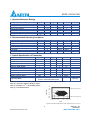
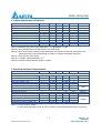
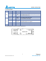
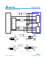
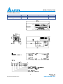
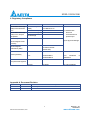
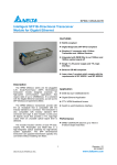
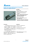
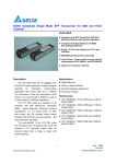
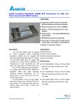
SFBD-155E2J1RM
Small Form Factor Bi-Directional Transceiver Module
for Fast Ethernet, ATM, SONET OC-3/SDH STM-1
FEATURES
RoHS compliant
2x5 Pin SFF Package with SC Receptacle
Single Mode Fiber, Bi-Directional
Transmission with 1310nm Transmitter and
1550nm Receiver
Link Distance up to 15km
Single +3.3V power supply and PECL logic
interface
Wave Solderable and Aqueous Washable
Bellcore GR-468 compliant
Laser Class 1 Product which comply with the
requirements of IEC 60825-1 and IEC 60825-2
Description
Application
DELTA’s SFF Bi-Directional transceiver is
designed for point-to-point Bi-Directional Optical
TTC TS-1000
ITU-T G.985
Network transmission. The module consists
multiple quantum well laser, InGaAs PIN,
Preamplifier and WDM filter in a high-integrated
optical sub-assembly, and it receives up to
155Mbps of continuous data at 1550nm, and
transmits 155Mbps of continuous data at 1310nm.
The module is contained in a 2x5 SFF
industry standard package with a SC receptacle
IEEE 802.3ah 100BASE-BX/ Fast Ethernet
SONET OC-3/SDH STM-1/ ATM Network
FTTx Broadband Access System
Performance
connector, and support LVTTL transmitter disable
input, LVPECL electrical signal Interface and
receiver signal detect output.
SFBD-155E2J1RM data link up to 15km in
9/125um single mode fiber.
1
DELTA ELECTRONICS, INC.
Revision: S0
12/20/2006
www.deltaww.com
SFBD-155E2J1RM
1. Absolute Maximum Ratings
Parameter
Storage Temperature
Storage Ambient Humidity
Power Supply Voltage
Signal Input Voltage
Optical Input Power (Peak)
Lead Soldering Temperature
Lead Soldering Time
Symbol
Ts
HA
VCC
Min.
-40
5
-0.5
-0.3
Typ.
Max.
85
95
5
Vcc+0.3
0
260
10
Unit
ºC
%
V
V
dBm
ºC
sec
Min.
0
5
3.13
Typ.
Max.
70
85
3.47
230
100
155.52
15
Unit
ºC
%
V
mA
mVp-p
Mbps
km
Max.
-8
-5
Unit
dBm
dBm
dB
nm
nm
ns
ns
dB
dB
dB/Hz
TSOLD
tSOLD
Note
2. Recommended Operating Conditions
Parameter
Ambient Operating Temperature
Ambient Humidity
Power Supply Voltage
Power Supply Current
Power Supply Noise Rejection
Data Rate
Transmission Distance
Symbol
TA
HA
VCC
ICC
3.3
10
Note
Without air flow
Non-condensing
100Hz to 1MHz
3. Optical Specification of Transmitter
Parameter
Average Launched Power
Launched power (Peak.)
Extinction Ratio
Center Wavelength
Spectrum Width (RMS)
Optical Rise/Fall Time
Total Jitter
Optical Transmitter Reflectance
Optical Return Loss Tolerance
Relative Intensity Noise
Output Eye Mask
Symbol
PO
Min.
-14
Typ.
-11
ER
λC
σ
tr/tf
tJ
8.5
1260
1310
1360
6
1.3
1
-14
ORLT
14
RIN
-116
Compliant with Bellcore TR-NWT-000253
and ITU recommendation G.957
Note
Note (1)
Note (2)
Note (3)
Note (4)
Note (1). Launched power (avg.) is power coupled into a 9/125um single mode fiber.
Note (2). These are unfiltered 20-80% values.
Note (3). Measure at 223-1 NRZ PRBS pattern.
Note (4). Eye Mask definition
1.20
Amplitude
1.00
Mean level of logical "1"
0.80
0.50
0.20
0.00
Mean level of logical "0"
-0.20
0.00 0.15
0.35
0.65
0.85 1.00
Time
Optical Pulse Mask with Bessel Filter Specified in ITU-T G.957
2
DELTA ELECTRONICS, INC.
Revision: S0
12/20/2006
www.deltaww.com
SFBD-155E2J1RM
4. Optical Specification of Receiver
Parameter
Input Optical Wavelength
Receiver Sensitivity
Input Saturation Power (Overload)
Signal Detect -Assert Power
Signal Detect -Deassert Power
Signal Detect Hysteresis
Optical Receiver Reflectance
Output Data Rise/Fall time
S/X Endurance
Optical Isolation
Symbol
λIN
PIN
PSAT
PA
PD
PA-PD
Min.
1480
-3
-44
0.5
Typ.
Max.
1600
-30
-30
2.5
6
-14
1.5
10
tr/tf
25
-10
Unit
nm
dBm
dBm
dBm
dBm
dB
dB
ns
dB
dB
Note
Note (1)
Note (2)
Note (3)
Note (4)
Note (5)
Note (6)
23
Note (1). Measured with 1520nm, ER=10dB; BER =<10 @PRBS=2 -1 NRZ
Note (2). When SD deasserted, the data output is Low-level (fixed)
Note (3). When the terminal is viewed from the optical path, the reflection toward the optical path of the
optical signal with a central wavelength of 1480nm to 1580nm transmitted to terminal.
Note (4). These are 20%~80% values
Note (5). X=10 MHz, Rectangular BER =10-10
Note (6). Receiver isolation between 1260nm ~1360nm
5. Electrical Interface Characteristics
Parameter
Transmitter
Total Supply Current
Differential line input Impedance
Differential Data Input Swing
Data Input Voltage- High
Data Input Voltage- Low
Transmitter Disable Input-High
Transmitter Disable Input-Low
Receiver
Total Supply Current
Differential Data Output Swing
Data Output Voltage-High
Data Output Voltage-Low
Signal Detect Output Voltage-High
Signal Detect Output Voltage-Low
Symbol
Min.
ICC
RIN
VDT
VIH-VCC
VIL-VCC
VDISH
VDISL
80
300
-1.165
-1.810
2
0
ICC
VDR
VOH-VCC
VOL-VCC
VOH-VCC
VOL-VCC
400
-1.085
-1.830
-1.085
-1.830
Typ.
100
Max.
Unit
Note
A
120
1600
-0.880
-1.475
VCC+0.3
0.8
mA
Ohm
mVp-p
V
V
V
V
Note (1)
B
2000
-0.880
-1.555
-0.880
-1.555
mA
mVp-p
V
V
V
V
LVPECL
LVTTL
Note (1)
LVPECL
Note (1). A (TX)+ B (RX) = 230mA
(A: Not include termination circuit; B: using a resister of 150Ω between Data-output and ground)
3
DELTA ELECTRONICS, INC.
Revision: S0
12/20/2006
www.deltaww.com
SFBD-155E2J1RM
6. Pin Description
Tx/Rx
Rx
Tx
Pin No.
I/O
Pin Name
Description
1
VeeR
Receiver Ground
2
VccR
+3.3V Receiver Power Supply
Normal Optical Input indicated by logic “High”, and No Optical
Input indicated by logic “Low”.
3
O
SD
4
O
RD(n)
Inverted Receiver Data Output
5
O
RD(p)
Non-Inverted Receiver Data Output
6
VccT
+3.3V Transmitter Power Supply
7
VeeT
Transmitter Ground
8
I
Tx_Dis
LVTTL Logic “High” to Disable Transmitter, and Enable
Transmitter by Logic “Low” or “Open”.
9
I
TD(p)
Non-Inverted Transmitter Data Input
10
I
TD(n)
Inverted Transmitter Data Input
MS
Mounting studs/ connect this pin to Chassis ground
Note. EMI shielding lead must be connected to Signal ground
MS
Bottom View
MS
4
DELTA ELECTRONICS, INC.
Revision: S0
12/20/2006
www.deltaww.com
SFBD-155E2J1RM
7. Recommended Interface Circuit
D E L T A S F F M odule
1u H
6. V ccT
3 .3 V
1 0u F
1 00 nF
1 00 n F
1u H
8 . T x _D is
T x _E nable
T ransm itter
9. T D (p)
T x-C oupled
interface
1 0 . T D (n )
7. V eeT
P rotocol IC
2 . V ccR
S erD es IC
1 0u F
10 0n F
5 . R D (p )
R x-C oupled
interface
4 . R D (n )
R eceiver
3. SD
SD
2 70 o hm
1. V eeR
D C - C o u p led in terface
3 .3 V
H o st
B o ard
82ohm
H o st
B o ard
Z 0=50ohm
DELTA
M o d u le
130ohm
130ohm
DELTA
M o d u le
Z0=50ohm
Z0=50ohm
3 .3 V
100nF
Z 0=50ohm
82ohm
130ohm
A C - C o u p led in terface
T x -C ou p led
in terface
RES0
100nF
RES0
82ohm
82ohm
130ohm
3 .3 V
3 .3 V
D C - C o u p led in terface
3 .3 V
R x-C o u pled
in terface
3 .3 V
130ohm
H o st
B o ard
RES1
RES2
82ohm
100nF
Z 0=50ohm
H o st
B o ard
Z 0=50ohm
Z 0=50ohm
DELTA
M o d u le
Z 0=50ohm
DELTA
M o d u le
100nF
RES1
130ohm
A C - C o u p led in terface
RES2
150ohm
150ohm
82ohm
3 .3 V
3 .3 V
R E S 0 , R E S 1 an d R E S 2 d ep en d o n S erD es ch ip u sed
5
DELTA ELECTRONICS, INC.
Revision: S0
12/20/2006
www.deltaww.com
SFBD-155E2J1RM
8. Outline Dimensions
Parameter
Mechanical Dimensions
Connector Type
Unit
mm
-
Description
Note
48.3x13.5x9.6
SC connector
IEC-61754-4
.
J
r
e
t
p
a
h
c
b
u
S
R
F
nC
o
i
t1
a2
i
ta
d
c
,
s
u
d
dr
r
Aa
o
d
r
Dn
P
F
a
rh
t
s
e
t
s
e
ai
wn
c
L
sa
1e
m
ir
l
sm
p
o
s
f
a
r
l
oe
C
C
p
W eek (52W eeks/Year) : 1月 2日 =01
6
DELTA ELECTRONICS, INC.
Revision: S0
12/20/2006
www.deltaww.com
SFBD-155E2J1RM
9. Regulatory Compliance
Feature
Electrostatic Discharge
Test Method
Reference
Performance
Human Body Model MIL-STD-883E Method 3015.7
(ESD) to the Electrical
Pins
(HBM)
Electrostatic Discharge
(ESD) to the Simplex
Receptacle
Contact Discharge
Machine Model (MM) EIA-JESD22-A115
Air Discharge
IEC/EN 61000-4-2
IEC/EN 61000-4-2
IEC/EN 61000-4-3
Radio Frequency
Electromagnetic Field
Immunity
(1) Satisfied with
electrical
characteristics of
product spec.
(2) No physical damage
FCC Part 15 Class B
EN 55022 Class B
(CISPR 22A)
Electromagnetic
Interference (EMI)
Laser Eye Safety
EIA-JESD22-A114
FDA/CDRH
FDA 21CFR 1040.10, 1040.11
CDRH File # 0420993
TUV
IEC/EN 60825-1
IEC/EN 60825-2
TUV
Certificate
R50032471
TUV
IEC/EN 60950
UL/CSA
UL 60950
#
Component Recognition
UL File # E239394
Appendix A. Document Revision
Version No.
S0
Date
2006-12-20
Description
Preliminary Datasheet
7
DELTA ELECTRONICS, INC.
Revision: S0
12/20/2006
www.deltaww.com