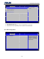
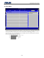
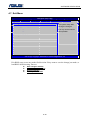
1
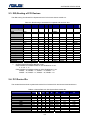
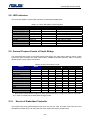
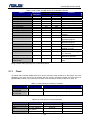
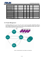
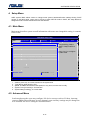
SOFTWARE PECIFICATION
6
Chapter
Software Specifications
Get to know more about the Z93E series Notebook with a detailed look at
the software specifications.
T
he information contained in the chapter can be quite useful when you are troubleshooting the
system’s hardware. Each item has its individual usage for you to understand the software side of
the notebook’s architecture.
6-1
SOFTWARE PECIFICATION
1.
Introduction
This BIOS specification describes the major features of key components and system BIOS, the usage of
general purpose input/output (GPIO) pins of south bridge (SB) and embedded controller (EC), the
hardware IRQ routing and resource allocation, setup menu, system power management mechanism,
system security policy, and so on.
The system BIOS is designed to comply with all industry standards, specifications, and design guides
of PC/AT system including:
z
z
z
z
z
z
z
z
z
z
z
z
z
z
z
z
z
PC 2001 System Design Guide, Version 1.0
Advanced Configuration and Power Interface (ACPI) Specification, Revision 1.0b & 2.0
Simple Boot Flag Specification, Revision 2.0
PCI BIOS Specification, Revision 2.0
Plug and Play BIOS Specification, Version 1.0A
Extended System Configuration Data (ESCD) Specification
System Management BIOS (SMBIOS, i.e. DMI) Reference Specification, Version 2.3
System Management Bus BIOS Interface Specification, Revision 1.0
BIOS Boot Specification
Multiprocessor Specification, Revision 1.4
Universal Serial Bus Specification, Revision 1.1 & 2.0
Universal Host Controller Design Guide
Universal Serial Bus PC Legacy Compatibility Specification
Enhanced Host Controller Interface Specification for Universal Serial Bus, Revision 1.0
PCI Express Base Specification, Revision 1.0
PCI Local Bus Specification, Revision 2.3
PCI Bus Power Management Interface Specification
6-2
SOFTWARE PECIFICATION
2. Hardware Overview
2.1. Key Components
The onboard key components and optional mini-PCI modules are listed at table 2-1 and 2-2.
Table 2-1 Key Component List
CPU
Item
Intel
Vendor
Part’s Name
Dothan
North Bridge
South Bridge
VGA
USB
LAN
Cardbus
IEEE1394
Azalia Audio
Intel
Intel
Intel
Intel
Realtek
Ricoh
Ricoh
Realtek
915-GM
ICH6-M
915-GM
ICH6-M
RTL8100CL
R5C841
R5C841
ALC880
Clock Gen.
Thermal
Azalia Modem
Super IO
Embedded
Controller
ICS
MAXIM
Realtek
ITE
Mitsubishi
ICS954213
MAX6657
ALC880
ITE8705
M38857
Features
Geyserville III Speed-Step
Thermal Monitor 2
Table 2-2 Optional Component List
Item
Wireless LAN
TV turn Card
FM module
Blue Tooth
Vendor
Intel
AVerMedia
MAOTEK
ASUS
Part’s Name
CalexicoChipset
M103 & M104
JFR-600
BT-183
Revision
2.2. Bus Number Allocation
The bus number allocation for PCI-to-PCI, PCI Express Graphic and CardBus bridges are listed at table
2-3.
Table 2-3 Bus Number Allocation
Device
Bus#
Dev#
Fun#
PCI-to-PCI
Bridge
CardBus Bridge
0
30
0
1
1
0
Primary Secondary Subordinate Onboard Devices On
Secondary Bus
Bus#
Bus#
Bus#
0
1
2
LAN; CardBus; 1394;
MiniPCI (WLAN)
1
2
2
P.E.G.* Bridge
X
X
X
X
X
*: P.E.G. – PCI Express Graphic
6-3
X
PCI Express Graphic
Controller
SOFTWARE PECIFICATION
2.3. IRQ Routing of PCI Devices
The IRQ routing of onboard PCI chipsets and mini-PCI slot are shown at table 2-4.
Table 2-4 IRQ Routing of Onboard PCI Chipsets and mini-PCI Slot
Device
Vendor
IDSEL
Bus#
Dev# Fun# INTA
P.E.G. Bridge
Intel
*
0
1
0
PIRQA
Intel
VGA
Azalia Controller Intel
*
*
0
0
2
27
0
0
PIRQA
PIRQA
Intel
*
0
29
0
PIRQH
USB #0
Intel
*
0
29
1
USB #1
Intel
*
0
29
2
USB #2
Intel
*
0
29
3
USB #3
Intel
*
0
29
7
PIRQH
EHCI
Intel
*
0
31
1
PIRQC**
IDE #0 (PATA)
Ricoh
AD17
1
1
0
Cardbus
Ricoh
AD17
1
1
1
1394
Ricoh
AD17
1
1
2
SD Card
PIRQB
Ricoh
AD17
1
1
3
PIRQB
Memory Stick
AD17
1
1
4
PIRQB
XD Picture Card Ricoh
Marvel
AD16
1
0
0
PIRQE
LAN
AD19
1
3
0
PIRQG
MiniPCI1
AD189
1
2
0
PIRQH
MiniPCI2
*:
Chipset Internal Routing
**: Chipset Internal Routing at NATIVE mode
IRQs Available for PIRQA~PIRQH on PIC-Enabled O.S. are:
3, 4, 5, 6, 7, 11
IRQs Available for PIRQA~PIRQH on APIC-Enabled O.S. are:
PIRQA – 16, PIRQB – 17, PIRQC – 18, PIRQD – 19
PIRQE – 20, PIRQF – 21, PIRQG – 22, PIRQH – 23
INTB
INTC
INTD
PIRQD
PIRQC
PIRQA
PIRQC
PIRQD
PIRQH
PIRQG
2.4. PCI Device IDs
The vendor/device and sub-system/sub-vendor IDs of onboard PCI devices are listed at table 2-5.
Table 2-5 Vendor/Device & Sub-System/Sub-Vendor IDs
Device
Host Bridge
VGA
LPC
PATA IDE
USB0
USB1
USB2
USB3
EHCI
Azalia controller
LAN
Cardbus
Vendor Bus
Intel
Intel
Intel
Intel
Intel
Intel
Intel
Intel
Intel
Intel
Realtek
Ricoh
0
0
0
0
0
0
0
0
0
0
1
1
Dev. Fun. Vendor Device
ID
ID
0
0
8086
2590
2
0
8086
2592
31
0
8086
2641
31
1
8086
266F
29
0
8086
2658
29
1
8086
2659
29
2
8086
265A
29
3
8086
265B
29
7
8086
265C
27
0
8086
2668
0
0
10EC
8139
1
0
1180
0476
6-4
Sub-Vendor
ID
1043
1043
1043
1043
1043
1043
1043
1043
1043
1043
1043
1043
Sub-System
ID
10B7
1882
10B7
10B7
10B7
10B7
10B7
10B7
10B7
10B3
1045
10B7
SOFTWARE PECIFICATION
1394
SD Card
Memory stick
XD Picture Card
Mini-PCI1
Mini-PCI2
Ricoh
Ricoh
Ricoh
Ricoh
Intel
Intel
1
1
1
1
1
1
1
1
1
1
3
2
1
2
3
4
0
0
1180
1180
1180
1180
option
option
0552
0822
0592
0852
option
option
1043
1043
1043
1043
1043
1043
10B7
10B7
10B7
10B7
10B7
10B7
The SSID/SVID of Modem is 1043/1966 in the codec.
2.5. Chipset Strapping
The strapping signals are used for static configuration. Table 2-6 and 2-7 show the strapping pins’ driven
states of SB and EC for the system.
GPIO I/O
Multiplex
Pin Type
W/ Pin
I REQ_5#
0
I REQ_6#
1
I PIRQE#
2
I PIRQF#
3
I PIRQG#
4
I PIRQH#
5
I BMBUSY#
6*
I None
7
I None
8
I OC4#
9
I OC5#
10
I SMBALERT#
11
I None
12
I None
13
I OC_6#
14
I OC_7#
15
O GNT6#
16
O GNT5#
17
O STP_PCI#
18*
O None
19
O STP_CPU#
20
O None
21
22** N/A N/A
O None
23
O None
24
O None
25
26
27
28
I
I
I
SATA0_GP
None
None
29
30
31
32
33
34
I
I
I
O
I
O
SATA1_GP
SATA2_GP
SATA3_GP
CLKRUN#
None
None
Table 2-6 ICH6 GPIO Definition
Usage
NOT USED
NOT USED
PIRQE#
NOT USED
PIRQG#
PIRQH#
BMBUSY#
NOT USED
EXTSMI#
OC4#
OC5#
NOT USED
KB_SCI#
SIO_SMI#
NOT USED
NOT USED
NOT USED
NOT USED
STP_PCI#
PWRLED_1HZ
STP_CPU#
BACK_OFF#
Description
N/A
N/A
Not as GPIO
Pull High 3V
Not as GPIO
Not as GPIO
No GPIO6
Pull High 3V
EC’s SMI event trigger pin
USB_OC_4#
USB_OC_5#
N/A
EC’s SCI event trigger pin
SIO’s SMI event trigger pin
Pull High 3V
Pull High 3V
N/A
N/A
Not as GPIO
Power LED will be blinking at suspending state.
Not as GPIO
Back light on/off control pin
LOW – On, HIGH - Off
N/A
N/A
FWH_WP#
Firmware Hub EEPROM write protection pin
802_LED_EN# Indicates that Wireless LAN is on
CB_SD#
Assert LOW to meet power sequence of Ricoh’s
Cardbus controller before entering S3 state and keep
asserted at S3.
SATA_DET#0 Not as GPIO
NOT USED
N/A
OP_SD#
Avoid the Audio noise
Before system runs the code of POST, pulls low.
Before the ACPI, pull high. After the ACPI, free it.
PCB_ID2
Main board revision identification pin#0
PCB_ID0
Main board revision identification pin#0
PCB_ID1
Main board revision identification pin#0
CLKRUN#
Not as GPIO
CPUFAN_SPD_A Indicate the CPU Fan speed
WLAN_ON#
WLAN on/off control pin
LOW – On, HIGH - Off
6-5
SOFTWARE PECIFICATION
35**
36**
37**
38**
39**
40
41
42**
43**
44**
45**
46**
47**
48
N/A
N/A
N/A
N/A
N/A
I
I
N/A
N/A
N/A
N/A
N/A
N/A
O
49
O
N/A
N/A
N/A
N/A
N/A
REQ4#
LDRQ1#
N/A
N/A
N/A
N/A
N/A
N/A
GNT4#
CPUPWRGD
N/A
N/A
N/A
N/A
N/A
PANEL_ID0
PANEL_ID1
N/A
N/A
N/A
N/A
N/A
N/A
GAIN_AMP_K#
H_PWRGD
N/A
N/A
N/A
N/A
N/A
Not needed for LCD supporting DDC
Not needed for LCD supporting DDC
N/A
N/A
N/A
N/A
N/A
N/A
Add the voltage for audio of DVD. Let the Audio have
loud volume.
LOW – 6v/v, HIGH - Normal
Not as GPIO
Table 2-7 M38859 GPIO Definition
Pin I/O
Type
2.0 O
Usage
Description
KBCRSM
Connected to power button for triggering power button press and release
events. Press 4 second turn off the system power.
KNC_P21
2.1 O
NOT USED, Pull High
BAT_LEARN
This pin is used for battery learning (refresh). Set it low for charging a
2.2 O
battery or batteries and high for discharging a battery or batteries.
DJ_LED
Indicates that is the Audio enable
2.3 I
SET_PLTRSTNS When setting this pin as high will gate the PCI_RST# signal from KBC,
2.4 O
LAN, CardBus devices. When setting this pin as low, those devices will
be reset by PCI_RST#.
CAP Lock Indicator.
2.5 O
CAP_LED
NUM_LED
Number Lock Indicator
2.6 O
SCROLL_LED# Scroll Lock Indicator
2.7 O
KBC_EXTSMI Any system management interrupt will be issued through this pin. It will
4.0 O
notify the system that some events happened.
EMAIL_LED
Email received indicator
4.1 O
WATCHDOG
Should create a event to EC, then clean the timer.
4.2 O
BT_ON
Blue Tooth On/Off detection pin;
4.3 O
LOW – Off, HIGH – On
KBCPURST_3Q CPU reset signal from KBC
4.4 O
KBC_GA20
This pin from KBC gates A20.
4.5 O
KBCSCI_3Q
SCI pin to notify system of runtime or wake up events from KBC.
4.6 O
CLKRUN#
4.7 I/O
Standard PCI clock run protocol
BAT_LLOW#
When the pin is set as low, it represents that battery is in very low
5.0 I
capacity.
FM_PSK#
FM Audio output pin;
5.1 I
LOW – Speaker, HIGH – head phone
5.2 I/O PWR_DJ_DETECT Power Button press detect pin.
LOW – Non_press, HIGH – Power button press
CLR_DJ#
Clear SWDJ_EN# status.
5.3 I
BAT_SEL
Indicates the battery type
5.4 I
HIGH – 8 Cell, LOW – 4 Cell
BAT1_IN_OC# Low level indicates that battery is existed.
5.5 I
FAN_DA1
5.6 O
It controls the FAN speed. S3 should pull Low
PORT_BAR_IN Set High For Port Bar
5.7 O
EMAIL#
It indicates that EMAIL button is pressed N/A
6.0 I
INTERNET#
It indicates that INTERNET button is pressed
6.1 I
MARATHON#
Read VID’s voltage
6.2 I
DISTP#
It indicates that Power4 Gear button is pressed. Can use for PAD Lock.
6.3 I
6-6
SOFTWARE PECIFICATION
6.4
6.5
I
I
6.6
I
6.7
7.0
7.1
7.2
7.3
7.4
7.5
7.6
7.7
O
I/O
I/O
I/O
I/O
I/O
I/O
I/O
I/O
ACIN
LID_KBC#
High level indicates that AC adapter is existed.
LID close/open detection pin;
LOW – closed, HIGH – open
SWDJ_EN#
If software DJ button is pressed, it will be latched on SWDJ_EN# and let
system know the software DJ have been launched. (GPI)
CHG_FULL_OC In AC mode only, indicates the battery is full charge.
TPAD_DAT
N/A
NC
N/A
NC
N/A
TPAD_CLK
N/A
NC
N/A
NC
N/A
BAT_SMD
N/A
BAT_SMC
N/A
2.6. System Management Bus Connections
The system has three independent system management bus (SMBus) interfaces on SB and EC chipsets,
respectively. The devices connected to these 3 host interfaces are shown at table 2-10 and 2-11.
Table 2-8 SMBus Connections on South Bridge
Device
1st DIMM Module
Address
1010000xb*
2nd DIMM Module
Clock Generator
1010001xb
1101001xb
Thermal Monitor
0101110xb
*:
Usage
Read DRAM timing and configuration stored on “Serial
Presence Detect” (SPD) device of a DIMM module for
determining memory size and optimum timing.
Ditto.
Disable unused clock source and enable spread
spectrum.
Set thermal trip and automatic fan on points; Provide
current temperature
Where x=1 – READ, x=0 – WRITE.
Table 2-9 SMBus Connections on Embedded Controller
Device
Smart Battery
Address
0001011xb
Usage
Access gas gauge for getting design/remaining
capacity, charging/discharging state, etc.
Smart battery is charged by the PIC, PIC16C534C. It is a processor, operating is independence.
2.7. Display Data Channels (DDC) and GMBus
The VGA controller supports display data channels (DDC) on LCD and CRT interfaces as well as SMBus
on SDVO. Thus, the VGA BIOS and driver could determine the resolution and timing of a display device
by reading its EDID data. The system BIOS doesn’t have to provide callback function for reporting LCD
type.
Table 2-10 DDC and GMBus Connections on VGA Controller
Device
LCD Panel
CRT Monitor
Address
Usage
Access EDID data for determining the resolution and
timing of the display device
Ditto.
6-7
SOFTWARE PECIFICATION
2.8. LED Indicators
The colors and states of system LED indicators are described at table below.
Table 2-11 Colors and States of LED Indicators
LED
Power
Power
Battery-Charging
Battery Low Power
Hard Disk
E-Mail
WLAN
AudioDJ
CAPS Lock
NUM Lock
SCROLL Lock
State
Steady On
Flashing
Steady On
Flashing
Flashing
Steady On
Steady On
Steady On
Steady On
Steady On
Steady On
Color
Indication
System power is supplied
S3 (suspend to RAM) state
Charge a battery or batteries
Battery capacity is below 10%
Access a hard drive
Have new E-mail(s)
Enable the WLAN
In the Audio DJ mode
2.9. General Purpose Events of South Bridge
The general-purpose inputs of the south bridge could trigger SCI, SMI, and/or wake-up events. These
inputs come from LID switch, EC, USB, LAN, modem, CardBus, and audio interfaces. Table 2-14 lists the
general-purpose event (GPE) connections.
Table 2-12 GPE Connections on SB
Source
GPE#
ACPI Mode
SMI
Wake
Legacy Mode
SCI
SMI
Wake**
V
V
V
SCI
Thermal (THRM#)
V
EC’s SCI Pin (GPI12)
V
EC’s SMI Pin (GPI8)
V
LAN’s PME*
V
Ring Indication (RI#)
V
V
Modem CODEC
Audio CODEC
V
USB0
V
USB1
V
USB2
V
USB3
V
EHCI
V
CardBus
V
V
*: PME – Power Management Event
**: Because the chipset doesn’t support S1 state and the BIOS do not support S3 state for none ACPI
O.S., either, it actually has no sleep state at legacy mode.
2.10.
Events of Embedded Controller
The internal keys and general-purpose input pins are the SCI, SMI, and WKI event sources of the
embedded controller (EC). The event sources of this system are shown at table below.
6-8
SOFTWARE PECIFICATION
Table 2-13 SCI, SMI, and WKI Events of Embedded Controller
Source
Notification
Code (Hex.)
Fn+F1 (FHK1)
Fn+F2 (FHK2)
Fn+F5 (FHK5)
Fn+F6 (FHK6)
Fn+F7 (FHK7)
Fn+F8 (FHK8)
Fn+F10 (FHK10)
Fn+F11 (FHK11)
Fn+F12 (FHK12)
E-Mail Button (P6.0)
Trigger Pin
ACPI Mode Legacy Mode
SCI
SMI
SCI
SMI
SCI
SMI
SCI
SMI
SCI
SMI
SCI
SMI
SCI
SMI
SCI
SMI
SCI
SMI
SCI
X
Function
Simulate a sleep button.
Switch wireless LAN on/off.
Decrease LCD brightness.
Increase LCD brightness.
Turn off LCD backlight.
Toggle display devices.
Turn audio volume on/off.
Decrease audio volume.
Increase audio volume.
Run E-Mail application
program.
Internet Button (P6.1)
SCI
X
Launch internet browser.
AP1 Button (P6.2)
SCI
X
Invoke a designated
application program.
AP2 Button (P6.3)
SCI
X
Invoke a designated
application program.
SMI
SMI
Fn+ESC (FHK13)
Break into debugger.
AC_IN (P6.4)
SCI
SMI
Notify if the AC power is
supplied or cut off.
LID Switch
SCI
SMI
Notify if the LID is closed
BAT_IN# (P5.5)
SCI
SMI
Notify if a battery is plugged
in or removed
DOCK_IN# (P?.?)
X
X
Notify if an IDE device is
attached or removed.
Any Key being pressed at
WKI
WKI
Wake up a system from sleep
suspend state
state.
NOTE: The WKI (KBCRSM) pin is connected to power button switch. So, it looks like a power button is
being pressed when typing any key of internal keyboard.
2.11.
Clock
To reduce EMI, it should disable these clock source not being used according. In the system, the clock
generator is the clock source for all chipsets and the memory controller provides the clock source for
DRAM DIMM modules. The connections of these clock sources are shown at table 2-14 and 2-15.
Table 2-14 Clock Source on Memory Controller
Source Pin(s)
Connected to
Control Register
DIMM #0
MCHBAR* + 18Ch[1-0]
SM_CK[4:3]
SM_CK[4:3]#
SM_CK[1:0]
DIMM #1
MCHBAR + 10Ch[1-0]
SM_CK[1:0]#
*: GMCH Register Range Base Address (Bus#0/Dev#0/Func#0/Reg#44h).
Table 2-15 Clock Source on Clock Generator
Source Pin(s)
96MhzT/C
27Mhz
48Mhz
REF0
Connected to
Control Register
DREFCLK
N/A
CLK_SIO_48M and
CLK_USB48
CLK_ICH14
Byte1 [7]
Byte1 [6]
Byte1 [5]
Byte1 [4]
6-9
Free Running
SOFTWARE PECIFICATION
REF1
CPUCLKT/C1
CPUCLKT/C0
PCICLK5
PCICLK4
PCICLK3
PCICLK2
PCICLK1
PCICLK0
PCICLK_F1
PCICLK_F0
CPUCLK2/SRCCLK5
SRCCLKT/C4
SRCCLKT/C3_STAT
SRCCLKT/C2
SRCCLKT/C1
SRCCLKT/C0
CLK_SSC_IN
CLK_CPU_BCLK
N/A
CLK_Mini PCI1
CLK_KBCPCI
CLK_LANPCI
CLK_CBPCI
CLK_MiniPCI2
CLK_SIOPCI
CLK_ICHPCI
CLK_FWHPCI
CLK_MCH_BCLK
CLK_MCH_3GPLL
N/A
CLK_PCIE_ICH
N/A
N/A
Byte1 [3]
Byte1 [2]
Byte1 [1]
Byte2 [7]
Byte2 [6]
Byte2 [5]
Byte2 [4]
Byte2 [3]
Byte2 [2]
Byte2 [1]
Byte1 [0]
Byte3 [7]
Byte3 [5]
Byte3 [4]
Byte3 [3]
Byte3 [2]
Byte3 [1]
6-10
Y
Y
Y
Y
N
Y
N
N
SOFTWARE PECIFICATION
3. BIOS Function
The main features of the BIOS are shown at table 3-1. It’s major change is not supporting APM function
because all supported Operating Systems except DOS are ACPI-Enabled and the core chipset doesn’t
support S1 sleep (power on suspend) state. It, thus, has no suspend state available at DOS.
Table 3-1 Features of System BIOS
Item
Description
AMI CORE8;
4Mbits Firmware Hub (FWH) EEPROM
CPU / Cache
Automatic frequency and cache size detection;
Dynamic CPU speed control at Windows XP (“Windows Native Processor
Performance Control”) and Windows 2000 (“Intel SpeedStep Technology Applet”);
Static CPU speed control during POST and at DOS.
DRAM
Sizing and timing detection by SPD.
HDD/CDROM
4-drive, Fast DMA, UDMA, fast PIO, block PIO, 32-bit IO, SMART disk, and INT
13 extensions support; automatic model typing, size detection, and parameters
setting (drive geometry, transfer mode, block size, LBA); bootable CDROM; hot
swapping.
FDD
N/A
Booting
Quiet boot; quick boot; multi-boot from HDD, CDROM, LAN (PXE), and USB
devices peripheral; boot sequence control at setup menu and pop-up boot
selection menu.
Setup Menu
Press F2 to enter setup menu during POST. For details, please refer to setup
menu section.
Boot Selection Menu Press ESC to pop-up this menu to select a boot device for one time.
Display
Multiple P.E.G. controller support; LCD, CRT, and TV presence detection and
toggle.
Keyboard
US/JP/EU internal keyboards and USB keyboard support.
Mouse
Internal touch pad, PS/2 mouse, and USB mouse Support.
Parallel port
N/A
Security
User & Supervisor password control for setup menu and boot;
Hard disk locking and password-freezing control;
USB, LAN, WLAN, MODEM, CardBus, and 1397 interfaces-disabling control.
PnP
Legacy ISA, PnP ISA, PCI and PCIExp devices auto-configuration;
PnP ISA and PCI run-time BIOS services support.
APM
Not support.
ACPI
C0, C1, C2, C3 (or C4), S0, S3, S4, and S5 power management states; control
method battery; proprietary on-screen display utility support.
SMBus
SMBus run-time BIOS services.
DDC
Display Data Channel is supported by built-in VGA BIOS.
SMBIOS (DMI)
System Management BIOS v.2.3 support.
Windows DMI data update interface support.
M-Mode
Dynamic CPU speed control.
Flash
EzFlash during POST; DOS and Windows flash interface support.
It provides a very simple boot flag register or variable that can be used by an operation
Simple Boot Flag
BIOS
system to communicate boot options to the system firmware and add-in card option ROMs.
This allows firmware and operation systems to automatically optimize their behavior and
boot performance base on the installed operation system and previous boots.
Others
Daylight savings time; Fast A20; 32-bit BIOS services; graphic setup menu
(English only).
3.1. Memory
The BIOS automatically detects the amount of memory in the system and configure the DRAM timing
based on the SPD data of DIMM module(s) at beginning of POST (Power-On-Self-Test).
6-11
SOFTWARE PECIFICATION
3.2. Display
In system BIOS, it includes several copies of VGA BIOS for Intel’s built-in P.E.G. controller. The BIOS will
automatically detect the VGA chipset vendor and load VGA BIOS accordingly. The VGA BIOS callback
function and/or MBI interface are also ready for each VGA controller to select boot display device(s) and
toggle them. The display device combinations of each VGA controller are shown at tables in this section.
Additionally, the resolutions and timings of display devices are determined by their EDID data.
Table 3-2 Display Device Combinations for Intel’s VGA
Display Device(s)
Pipe A
Pipe B
CRT
Y*
N
LCD
N
Y
TV
Y
Y
CRT + LCD
N
Y
CRT + TV
Y
N
LCD + TV
N
N
CRT + LCD + TV
N
N
*: Y – could display on the pipe; N – couldn’t display on the pipe.
3.3. Enhanced IDE
The BIOS supports the LBA re-mapping method to translate the geometry of a hard disk drive and the
INT 13 extension functions for removable devices and hard drives. On the system, it has two built-in IDE
controllers: one is parallel ATA (PATA) interface and the other is serial ATA (SATA) interface that could be
configured to run at legacy IDE mode or AHCI mode. Both controllers support only one channel, i.e. two
controllers totally support two channels. The BIOS will configure these two IDE controllers based on the
attached IDE drives and user’s selection at setup menu. The configurations are shown at table below.
Table 3-3 PATA and SATA Configurations
Configuration
Selection
Compatible
Compatible
Compatible
Enhanced
Present Device(s)
None or PATA only
SATA only
SATA & PATA
Any
Controller
PATA
SATA
Enabled
Disabled
Disabled
Disabled
Disabled
Disabled
Enabled
Disabled
Running Mode
PATA
SATA
Legacy
Legacy
Legacy
Legacy
Native/AHCI
Because none of current Windows Operation Systems (O.S.) supports AHCI mode for IDE drives, it
will run into a blue screen when installing a Windows or failure to boot up an installed Windows not
loading AHCI mode driver if selecting “Enhanced” configuration. Please check out the README file of
Intel’s IAA driver to load the AHCI mode driver when installing a Windows.
Additionally, the BIOS also supports the IDE hot swapping function for the drive on PATA controller if
the booting hard disk drive is on SATA controller.
6-12
SOFTWARE PECIFICATION
3.4. Legacy USB
In addition to USB keyboard and mouse, the BIOS also support USB 2.0 and 1.1 peripheral devices
including flash, hard disk, and optical drives for Operating Systems having no USB driver. In DOS, it
should load an ASUS’s proprietary USB driver to support DVDROM/CDROM drives.
3.5. Plug and Play
The BIOS supports the PnP, PCI, and ACPI specifications for dynamically allocating system resources.
The resource allocation of system board devices is listed at table below.
Table 3-4 System Resource Allocation
Device
Connect
Type
Resources
I/O (Hex)
DMA Controller
Static
00~0F, 81~8F
PIC Controller
Static
20~21, A0~A1
IRQ at
PIC
IRQ at
APIC
DMA
Memory (Hex)
Local APIC
Dynamic
FEE00000~FEEx
xxxx
IOAPIC
Dynamic
FEC00000~FECy
yyyy
System Timer
Static
40~43
0
0
RTC
Static
70~75
8
8
System Speaker
Static
61
System Board
Static
80
NB Chipset (System
Board)
Static
SB Chipset (System
Board)
Static
400~41F,
480~4BF,
800~87F
Embedded
Controller
Static
60, 62, 64, 66
1
1
Math Coprocessor
Static
F0~FF
13
13
Touch Pad / PS/2
Mouse
Video Controller
Static
12
12
Static
Serial Port
(NO)
Fast IR / IrDA
Static
2F8
ECP, Parallel port
Static
378
FDC
(NO)
PATA IDE Controller
(Compatible Mode)
E0000~FFFFF
E0000000~
EFFFFFFF,
FED14000~
FED17FFF,
FED18000~
FED18FFF,
FED19000~
FED19FFF
3B0~3BB,
3C0~3DF
DISABLED
6-13
FED1C000~
FED1FFFF
11
A0000~BFFFF,
C0000~CFFFF
SOFTWARE PECIFICATION
SATA IDE Controller
(Compatible Mode)
(NO)
PATA IDE Controller
(Enhanced Mode)
Static
SATA IDE Controller
(Enhanced Mode)
(NO)
CardBus Controller
Dynamic
1394 Controller
Dynamic
Audio Controller
Modem Controller
Dynamic
Dynamic
USB Host Controller
Dynamic
LAN Controller
Dynamic
1F0~1F7, 3F6
14
14
3E0~3E1
WLAN Controller
Dynamic
Note:
1. The dynamic resource of devices will be changed if users change the settings.
2. The system has no super I/O.
3.6. Power Management
The BIOS supports C0, C1, C2, C3 (or C4), S0, S3, S4, and S5 power management states for
ACPI-Enabled Operating Systems. In DOS, it has no power management because the SB chipset
doesn’t support S1 sleep state. It doesn’t support Advanced Power Management (APM), either. Figure 1
shows the global system power states and transitions.
Figure 1 Global System Power States and Transitions
6-14
SOFTWARE PECIFICATION
3.6.1. C States
To enhance system performance and save battery life, the BIOS uses the _CST control method to
dynamically report the supported “C States” when powered by AC or by DC.
z
z
Powered By AC:
Powered By DC:
C2.
C2, C4
In _CST control method, it reports “level 4” I/O port at C3 state package buffer to force system
entering C4 state when an O.S. puts CPU to C3 state because C4 state is not a standard “C” state of
ACPI specification and not implemented by current Windows O.S. The system supports C2 pop up and
pop down function. The C0 and C1 states are supported on all power sources. Any IRQ, SMI#, SCI, bus
master, or FERR# event will bring the system to C0 state from C1, C2, C3, or C4.
For those O.S. such as Windows Me doesn’t recognize _CST control method, the BIOS always
reports the system supports C2 and C3 at “Fixed ACPI” (FACP) description table. The worst-case
hardware latency times of C2 and C3 are 10 and 100 microseconds, respectively.
3.6.2. Sleep States
1. S0 state: The CPU and all devices are working.
2. S3 state: The CPU and PCI busses are powered off. All PCI devices must either be powered-off or
isolated and the embedded controller is put into suspend sate. However, the system
memory and graphic frame buffer are powered and refreshed by the memory controller
and the graphics controller, respectively. The system provides a 32kHz clock (SUSCLK)
in this suspend mode to support refresh of these memory subsystems. Only enabled
“resume event” such as internal keyboard, RTC alarm, power button, LAN, WLAN,
Modem, USB device(s) can bring the platform out of this sleep state.
3. S4 state: The context of entire system devices and memory are saved to disk. All components are
powered-off and all clocks are stopped. Any enabled “resume event” such as power
button, RTC, and/or LAN can bring the platform out of the S4 state.
4. S5 state: Same as S4 except not saving system context.
Table 3-5 Wake Up Events
Resume Event
S3
S4
S5
Screen
RTC Alarm (IRQ 8)
Y
Y
Y
OFF
Power Button
Y
Y
Y
ON
LID Switch
Y
ON
Modem RI#
Y
OFF
PCI PME# (LAN)
Y
Y
Y
OFF
Azalia # (Modem CODEC)
Y
OFF
USB
Y
ON
Any Key*
Y
ON
*: The EC’s “Any Key” wake-up event pin is connected to the power button switch.
3.7. CPU Speed Control
To fulfill the Geyserville III technology of Intel’s Pentium-M CPU, the BIOS implements the ACPI control
methods including _PDC, _PCT, _PSS, and _PPC for supporting “Windows Native Processor
Performance Control” to dynamically change CPU speed based on system loading and power scheme
selected in Windows XP.
6-15
SOFTWARE PECIFICATION
z _PDC:
z _PCT:
z _PSS:
z _PCT:
Called by native processor performance driver to pass it’s capabilities to BIOS; The
BIOS saves the capability flag for other control methods. This flag indicates if a
native performance processor driver is loaded.
If native driver is loaded, the processor native interface is used for the Performance
Control Object by declaring the CPU’s performance control and status registers as
functional fixed hardware objects. Otherwise, the SMI interface is used for the
Performance Control Object by declaring the ACPI command (0x82) and status
(0x83) ports as performance control and status ports.
If native driver is loaded, reports the control and status values based on CPU’s
performance control and status registers. Otherwise, these values are reported
based on ACPI command and status ports.
Report “0” as the highest state to allow all states to be used when running on both
AC adapter and battery (DC).
The BIOS also supports “Enhanced Intel SpeedStep Technology System Management Mode
Interface” for Intel’s SpeedStep Applet in Windows 2000. The O.S. and Intel’s SpeedStep Applet program
will issue software SMI to get BIOS support. The default SMI port is 0B2h at Intel’s Applet program. Here
are functions on this SMI interface:
z DISABLE:
z INITIALIZE:
z CONTROL:
z GET STATUS:
z SET STATE:
z SET SETUP:
z GET INFO:
z GET STATES:
SMI Port = OS Command value located in ACPI FADT table offset 55.
Called by the O.S. supporting native processor performance control. The CPU
speed transition should be controlled by the O.S. The BIOS only responds to
get status and reports to the applet.
SMI Port = 81h. Detect and identify operating states of onboard CPU.
SMI Port = 82h, EAX = 47534982h, EBX = 0.
Enable or disable SMI applet interface.
SMI Port = 82h, EAX = 47534982h, EBX = 1.
Reports to the applet software the current CPU state, the maximum number of
states supported, the current available number of states, the SpeedStep
capability of the CPU, the setup mode, the AC status, the revision of this SMI
interface, and the current state of CPU throttling.
SMI Port = 82h, EAX = 47534982h, EBX = 2.
Initiate a transition to the requested state.
SMI Port = 82h, EAX = 47534982h, EBX = 3.
Save changes of operating mode to the CMOS register location of the setup
menu item for Intel’s Applet control.
SMI Port = 82h, EAX = 47534982h, EBX = 4.
Reports to the applet software the highest and lowest performance states as
well as the duty cycle of throttling.
SMI Port = 82h, EAX = 47534982h, EBX = 5.
Reports the frequency of all supported states.
For details, please refer to the Intel’s orange document “RS – Geyserville Technology BIOS Porting
Guide”.
3.8. Thermal Management
To prevent a CPU from being over-heated, the BIOS implements the active cooling policy to keep CPU
and system temperatures as low as possible. Additionally, the thermal control circuit (TCC) of a CPU is
also enabled to let it perform an automatic performance state transition to a lower operating point as
specified in the GV_THERM control register if the CPU temperature is over the maximum operating
temperature or to assert THERMTRIP# signal to shutdown the system if the CPU temperature keeps
rising and reaches a temperature where permanent damage to the processor is imminent. The
temperatures of these two trip points are set at on-die digital thermal sensor of a CPU in a factory and
different among all family and/or stepping CPUs.
The thermal trip points of the system are shown at table 3-8. The control mechanism for both ACPI
and legacy modes is as follows:
1.
Set the lowest bus ratio to control register GV_THERM and enable TCC control of a CPU to let
6-16
SOFTWARE PECIFICATION
2.
3.
4.
CPU automatically transit CPU speed back and forth near maximum operating temperature.
Initialize the automatic fan control thermal sensor to drive fan on temperature to 40℃ and turn fan
off near 35℃ if it was on. The fan will be automatically turned on and off.
At initialization or whenever a thermal trip event occurs, do the action for the first true condition
listed from highest to lowest priorities at first column in table 3-9.
In ACPI-enabled O.S., reports _AC0, PSV, and _CRT temperatures listed at table 3-8 as well as
implementing thermal zone related control methods (_TMP, _TSP, _SCP, _TC1, _TC2), name
objects (_PSL, _AL0), fan device node “PNP0C0B”, fan’s power resource (_STA, _ON, _OFF), and
event handler (_L00).
Table 3-6 Thermal Transition States
Temperature
Trend
Fan Off
CPU Temperature (℃) at Transition State
Tran. Tran. To Throttling Throttling Critical
CPU
Speed Lowest
Off
On
Shutdown Thermal
Back
Speed
(_PSV)
(_CRT)
Trip
Up
40
> 90*
100
105
125*
Down
35
< 85
90
*: Dothan Processor. Please see the “EMTS” document of a processor to check out these two values.
Fan On
(_AC0)
Table 3-7 Thermal Control Actions
*: The thermal sensor and CPU will automatically turn on/off fan and transit CPU speed, respectively.
**: +/- 2℃ to/from high and low thermal trip limits to prevent the CPU temperature from frequently
jumping back and forth at a transition state and triggering too many thermal events.
For overall ACPI BIOS thermal control activity, the thermal management can be categorized into two
strategies:
1.
A thermal device triggers an event to ACPI BIOS, the BIOS notifies to the Operating System
to process such event. The event trigger temperature setting of the device has an upper and
lower limit, when the CPU temperature goes above the upper limit or below the lower limit, the
6-17
SOFTWARE PECIFICATION
2.
thermal event become active.
Operating System reads current temperature (through ACPI BIOS) periodically and process
the thermal handler depends on its thermal policy.
3.9. Brightness Control of LCD
LCD brightness is controlled via Intel DPST (Display Power Saving Technology). It’s a advance power
saving of LCD. BIOS will corporate with VGA driver to control LCD brightness for max power saving
without impact user view. Intel DPST will analyze display image produced by the OS or application. Intel
DPST applies an image-specific enhancement to increase image contrast, brightness and or attributes
with decrease to backlight brightness. This produces an image with similar user-perceived quality as the
original image.
Without VGA driver: If users press Fn-F5/Fn-F6 (brightness down/brightness up), BIOS invoke video
BIOS function call to change brightness. This will change LCD brightness directly.
With VGA driver: If users press Fn-F5/Fn-F6 (brightness down/brightness up), BIOS invoke video
BIOS function call to change brightness. VGA driver will read it and update some setting accordingly.
Then set LCD brightness.
INT 10h Backlight Brightness Interface
Calling Registers:
AX
5F61h, Local Flat Panel Support function
BH
08h, Set Backlight Control sub-function
BL
Brightness Level Setting (0-255), where 0=minimum brightness
and 255= maximum brightness
Calling Registers:
AX
005Fh, Function supported and successful AX
015Fh, Function supported but failed
3.10.
Embedded Controller
As well as keyboard controller, the embedded controller also includes the smart battery host controller
and ACPI embedded controller (EC).
3.10.1. Functional Events
To easily adjust some system hardware settings such as flat panel backlight, audio volume, display
device(s) or quickly bring up some predefined applications, the system implements the combination hot
keys and buttons. When pressing those hot keys or buttons, the EC triggers SCI or SMI events
depending on if ACPI mode is enabled or not. Additionally, the EC also triggers SCI or SMI event when
plugging-in or removing an AC power adapter, a battery, or an IDE device at swapping bay. For the event
codes and types, please refer to the section entitled “Events of Embedded Controller”.
For SMI events, the EC’s SMI handler of BIOS at SMM mode will query the SMI notification code of
the EC event being triggered and dispatch its corresponding handler to toggle display devices, adjust
LCD brightness, adjust audio volume, or change device in/out state and trigger polarity accordingly. For
SCI events, the EC driver will query the notification code, say 2Ah, and call the corresponding _Q control
method, say _Q2A, to handle the event. In turn, the _Q control method notify ASUS’s proprietary ATK
driver to show On-Screen-Display (OSD) icons and do actions accordingly. Please refer to the ATK driver
specification for the notification values of those events.
6-18
SOFTWARE PECIFICATION
3.10.2. Wake-Up Event
The EC will be put into suspend state and powered when a system enters S3 state. It will pulse its
wake-up pin when any key of the internal keyboard is pressed. Because the wake-up pin is connected to
the power button switch, it, thus, seems to press the power button to wake the system.
3.10.3. Battery System
The battery system includes a charger and two smart batteries. Both charger and batteries are connected
to the SMBus host interface of EC. A general-purpose pin is used to select one of two batteries to be
connected to the SMBus interface at a time. The working mechanism of the battery system is as follows:
z
The charger will stop charge the battery when the following condition is detected.
- The temperature of the system is too high.
- The battery voltage is too high.
z
Battery Life is around 4/2.5 Hours for 8 cells & 4cells.
Note that the battery life depends on different configuration running. (E.g. the battery life is shorter
with CDROM running, the battery life is longer with document keyin only; battery life is short while power
management is disabled, battery life is longer while power management is enabled.)
z
Battery reading methodology is through power meter applet of control panel in Windows. The
BIOS passes battery information to ACPI-enabled O.S. via control methods _BIF and _BST.
z
When the battery capacity remains 10%*, the charger will generate a battery warning SMI at
none ACPI-enabled O.S. environment or a SCI at ACPI-enabled O.S. environment.
When AC power is supplied, the battery system will do the following action:
z
- The charger will charge the Battery.
- The Battery Charging Indicator will turn on if the battery is in changing mode.
- The “Battery Low” warning condition will be removed.
When AC or battery power is supplied or removed, the EC will trigger events and the EC driver will
call the _Q control methods for AC and battery to handle these power events and notify O.S. to
re-emulate the state and information of the battery system.
3.11.
Security
To protect storage data and system, the BIOS implements several security mechanisms including setup
menu protection, booting prevention, hard disk lock, I/O peripheral interface disable, and optional TMP
module function.
3.11.1. Setup Menu and Booting Security
There are a supervisor and a user password for entering setup menu and booting a system. It could
select to check these passwords only when entering setup menu. Please refer to “Security Menu” section
for detail.
3.11.2. I/O Interface Security
The supervisor of a system could disable the modem, LAN, wireless LAN, USB, CardBus, 1394, and
6-19
SOFTWARE PECIFICATION
optical drive devices at setup menu and limit user’s access right to re-enable them.
3.11.3. Hard Disk Drive Protection
A user could set a password on a hard disk drive to lock it. At same time, a back door master password is
also set on the drive. The hard disk will be locked when it’s being hard reset. During POST, the BIOS will
ask a user to input a password to unlock the drive. This password could be the user or master hard disk
password. If the master password is input, the hard disk lock function will be disabled forever unless
being re-locked again. Additionally, the user and master passwords are frozen after the drive is unlocked
to prevent them from being changed by any application program. This input master password would be
different everyday.
3.11.4. Trusted Platform Module (TPM) Based Security
The TMP module is an optional device and functions like a smart card. The BIOS will initialize it and load
it’s driver accordingly. However, it needs other licensed application program to utilize it for security.
3.12.
Crisis Recovery
A proprietary debug card is used for doing crisis recovery. The steps are:
1.
2.
3.
4.
5.
6.
7.
8.
3.13.
Prepare one ISA EPROM with correct bios image.
Insert the ISA EPROM into a debug card
Select SW1:ON and SW3:OFF on debug card
Plug the debug card into a system.
Turn on the system.
The BIOS will execute normal POST and turn on screen before automatically recovering the
system BIOS.
The BIOS will shutdown the system after finishing recovery.
Take out the debug card and turn on system power to boot from system BIOS.
Supported Utility
The BIOS supports 3 flash utilities that are running during POST, at DOS, or at Windows. In addition, it also
supports a DOS and a Windows SMBIOS (DMI) utility for changing data of type 1, 2,and 3.
3.13.1. Extended 32 Bits Application Interface
6-20
SOFTWARE PECIFICATION
4. Setup Menu
A5EP system BIOS allows users to change some system hardware/function settings during POST
(power on self test) stage, users may hit F2 key to enter SETUP mode in POST, the setup feature is
categorized into 6 menus described in next few sections
4.1. Main Menu
Main menu describes system overall information with some user changeable setting, it contains
below items:
AMI BIOS Setup Utility
Main
Advanced
Display
Security
Power
System Overview
AMIBIOS
Version
Boot
Exit
Use [ENTER], [TAB] or
[SHIFT-TAB] to select at
field.
: 200
Use [+] or [-] to configure
system Time.
Processor
Type
: Intel(R) Pentium (R) M
Speed
: 2133MHZ
System
Size
: 1008MB
System Time
System Date
[08:15:59]
[Thu 05/03/2005]
V02.56 (C) Copyright 1985-2004, American Megatrends, Inc.
1.
2.
3.
4.
5.
Version: [xxxx.xxx] Å Current version for the system bios
Type [String]: What kind for CPU
Speed: The BIOS auto detect CPU speed, It’s only show, so user don’t modify
System Time: [hh/mm/ss] Å Current time
System Date [mm/dd/yy] Å Current date
4.2. Advanced Menu
In advanced menu the users may configure I/O device resource such as I/O base, interrupt
vector or DMA (Direct Memory Access) channel, some auxiliary settings may be changed as
well. Detailed I/O device setting are described below:
6-21
SOFTWARE PECIFICATION
AMI BIOS Setup Utility
Main
Advanced
Display
Security
Power
Advanced Settings
Warning: Setting wrong values in below Sections may cause
system to malfunction
Boot
Exit
Configure the IDE
devices
► IDE Configuration
Start Easy Flash
Internal Pointing Device
Internal Numeric Pad Lock
[Enabled]
[Enabled]
V02.36 (C) Copyright 1985-2002, American Megatrends, Inc
1. IDE configuration: See 5.2.1
2. Internal pointing device: [Enable] Å Touch Pad enable/disable you can choice
3. Internal Numeric Pad Lock [Enable] Å Num LK (Number Lock) enable/disable
4.2.1. IDE Configuration
AMI BIOS Setup Utility
Advanced
IDE Configuration
► Primary IDE Master
► Primary IDE Slave
:
:
[Hard Disk]
[ATAPI CDROM]
V02.36 (C) Copyright 1985-2002, American Megatrends, Inc
6-22
While entering setup, BIOS
auto detect the presence of
IDE devices. This displays
the status of auto detection
of IDE devices.
SOFTWARE PECIFICATION
4.2.2. Primary Master/Slave IDE
AMI BIOS Setup Utility
Advanced
Select the type of device
connected of the system
Primary IDE Master
Device
Vendor
Size
LBA Mode
Block Mode
PIO Mode
Async DMA
Ultra DMA
S.M.A.R.T.
: Hard Disk
: HTS541080G9AT00
: 80.0GB
: Supported
: 16Sectors
:4
: Multiword DMA-2
: Ultra DMA-5
: Supported
Type
LBA/Large Mode
Block (Multi-Sector Transfer)
PIO Mode
DMA Mode
S.M.A.R.T.
32Bit Data Transfer
[Auto]
[Auto]
[Auto]
[Auto]
[Auto]
[Auto]
[Enabled]
V02.36 (C) Copyright 1985-2002, American Megatrends, Inc
At system boot, the Intel Ultra ATA Storage Driver configures each ATA/ATAPI device to transfer data at
particular transfer modes. These transfer modes are defined by ATA standards, and are either
Programmed I/O (PIO) or Direct Memory Access (DMA or UltraDMA) type transfers. The Intel Ultra ATA
Storage Driver usually configures devices for their fastest capable transfer modes; however, there may
be times when a different (perhaps slower) transfer mode is appropriate for a particular device or system
configuration.
For hard disk and CD-ROM drives BIOS detect them automatically. The users may enter the selected
(highlighted) item to get more detailed information, which contains 3 selectable setting:
[Auto]: BIOS default setting.
[User Type HDD]: Users may configure the disk geometry by changing below item:
z
Translation Methods
z
Cylinders
z
Head
z
Sector
z
Multi-Sector Transfer
z
Smart Monitoring
z
PIO Mode
z
Ultra DMA Mode
[None]: Hide the drive.
6-23
SOFTWARE PECIFICATION
4.3. Display Menu
AMI BIOS Setup Utility
Main
Advanced
Display
Security
Power
Boot
Exit
Select Boot display
devices(s).
Configure advance settings for displays
Boot Display devices:
[CRT+LCD]
TV Standard
[NTSC]
V02.36 (C) Copyright 1985-2002, American Megatrends, Inc
Boot Display devices: [LFP / CRT / CRT+LCD ]←Select boot display device, default mode is LFP&CRT
mode.
TV Standard: [NTSC/PAL/PAN_M/PAL_60/NTSC_J/PAL_CM/PAL_N/SCART_RGB]
6-24
SOFTWARE PECIFICATION
4.4. Security Menu
AMI BIOS Setup Utility
Main
Advanced
Display
Security
Security Settings
Supervisor Password
User Password
Power Saving
Boot
The password for this hard
drive can be set or cleared
here. Power must be cycled
for the hard drive to lock
: Not Installed
: Not Installed
Change Supervisor Password
Change User Password
Clear User Password
Boot Sector Virus Protection
I/O Interface Security
Exit
[Disable]
Hard Drive Security
Hard Disk Password: Not Installed
Primary Master HD Password
V02.36 (C) Copyright 1985-2002, American Megatrends, Inc
6-25
SOFTWARE PECIFICATION
AMI BIOS Setup Utility
Main
Advanced
Display
Security
Power Saving
Security Settings
Supervisor Password
User Password
Boot
Exit
The password for this hard
drive can be set or cleared
here. Power must be cycled
for the hard drive to lock
: Not Installed
: Not Installed
Change Supervisor Password
Change User Password
Clear User Password
Boot Sector Virus Protection
I/O Interface Security
[Disable]
Hard Drive Security
Hard Disk Protection
[Disabled]
V02.36 (C) Copyright 1985-2002, American Megatrends, Inc
BIOS supports two levels of password for security protection:
1.
2.
3.
Supervisor password:
Users may set, change or erase system password, the password data is saved in non-volatile
device (CMOS), system password check is done during POST (Power On Self Test). The
BIOS will prompt a dialog message to ask user for password check when:
The system has password stored, and
“Password on boot” setting in BIOS SETUP is enabled.
If password verification fails for 3 times, the system BIOS will halt the machine to inhibit users
from operating.
User Password
If other has modified your setting of BIOS, you can setting the function [Enable],
And type in your password and confirm, don’t modify BIOS setting if no password.
Hard disk password:
Users may set, change or erase hard disk password, the password data is stored in the drive
itself, the BIOS prompts a dialog message for hard disk password verification whenever it finds
the hard disk locked in POST.
If hard disk password verification fails for 3 times, the system BIOS will halt the machine to
inhibit users from operating.
6-26
SOFTWARE PECIFICATION
4.5. Power Menu
AMI BIOS Setup Utility
Main
Advanced
Display
Power management Setting
LCD Power Saving
Wake-up On LAN
Security
[Enabled]
[Disabled]
Power
Boot
Exit
Press Enter to start
calibrating a battery. The
calibration should charge
the battery to full and then
discharge it to empty.
► Start Battery Calibration
V02.31 (C) Copyright 1985-2002, American Megatrends, Inc
1
2
3
LCD Power Saving: LCD exhausts the most part of power while the system is operating. A5EP
notebook system BIOS support auto backlight saving mode. When the system BIOS detects AC
adapter removal, the LCD brightness is tuned down to 80﹪of its original setting, and back to normal
when AC adapter is back inserted.
Wake-Up On LAN: Enable it, system can wake up form magic package from Ethernet.
Battery refresh: After long time incomplete charge/discharge cycles, the battery meter becomes
less and less accurate (the total power capacity is not significantly affected, however). Battery gauge
needs to “learn”, this item helps users to recalibrate the battery gauge. In the learning process,
users need to follow system BIOS instruction to I Insert/remove the AC adapter so that a complete
reset and learning cycle may start.
6-27
SOFTWARE PECIFICATION
4.6. Boot Menu
AMI BIOS Setup Utility
Main
Advanced
Display
Security
Boot Settings
Power Saving
Boot
Exit
Configure Settings during
system Boot
► Boot Setting Configuration
► Boot Device Priority
► Hard Disk Drives
► Removable Drives
► ATAPI CDROM Drives
Onboard LAN BOOT ROM
[Disabled]
V02.31 (C) Copyright 1985-2002, American Megatrends, Inc
In this menu users can decide the boot sequence, as long as the device with highest boot priority
exists, system BIOS will boot from it, device boot priority is adjusted by pressing “+”,”-“ or
space key on the selected (highlighted) item. 4 bootable devices for A5EP system are listed in
this menu (BIOS default boot sequence):
1.
2.
3.
4.
Removable device: ← Legacy floppy.
IDE Hard Drive: ← hard disk.
ATAPI CD-ROM: ← CD-ROM
Network Boot: ← LAN
6-28
SOFTWARE PECIFICATION
4.7. Exit Menu
AMI BIOS Setup Utility
Main
Advanced
Display
Security
Exit Options
Power Saving
Boot
Exit
Exit system setup after
saving the changes.
Save Changes and Exit
Discard Changes and Exit
F10 key can be used for
this operation.
Discard Changes
Load Optimal Defaults
V02.36 (C) Copyright 1985-2002, American Megatrends, Inc
Exit BIOS setup, users may make final decision if they want to save the change just made, or
load BIOS default setting, lists are:
z
z
z
z
Save changes and Exit
Discard changes and Exit
Discard Changes
Load Optimal Defaults
6-29