1
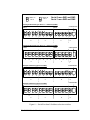
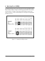
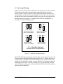
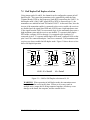
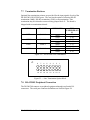
DS-200/300
Two Channel RS-422/485 Asynchronous
Enhanced Serial Adapter
for ISA compatible machines
INTERFACE CARDS FOR IBM PC/AT AND PS/2
User's Manual
QUATECH, INC.
5675 Hudson Industrial Parkway
Hudson, Ohio 44236
TEL: (330) 655-9000
FAX: (330) 655-9010
http://www.quatech.com
Warranty Information
Quatech Inc. warrants the
DS-200/300
to be free of defects for one (1) year from the
date of purchase. Quatech Inc. will repair or replace any adapter that fails to perform under normal operating
conditions and in accordance with the procedures outlined in this document during the warranty period. Any
damage that results from improper installation, operation, or general misuse voids all warranty rights.
The authors have taken due care in the preparation of this document and any associated software
program(s). In no event will Quatech Inc. be liable for damages of any kind, incidental or consequential, in
regard to or arising out of the performance or form of the materials presented herein and in the program(s)
accompanying this document. No representation is made regarding the suitability of this product for any
particular purpose.
Quatech Inc. reserves the right to edit or append to this document or the product(s) to which it
refers at any time and without notice.
Please complete the following information and retain for your records. Have this information available when
requesting warranty service.
Date of purchase:
Model Number:
DS-200/300
Product Description:
Two Channel RS-422/485 Asynchronous Enhanced Serial Adapter
Serial Number:
DS-200/300 User's Manual
i
© 1998, Quatech, Inc.
NOTICE
The information contained in this document cannot be reproduced in any
form without the written consent of Quatech, Inc. Likewise, any software
programs that might accompany this document can be used only in accordance
with any license agreement(s) between the purchaser and Quatech, Inc. Quatech,
Inc. reserves the right to change this documentation or the product to which it
refers at any time and without notice.
The authors have taken due care in the preparation of this document and
every attempt has been made to ensure its accuracy and completeness. In no event
will Quatech, Inc. be liable for damages of any kind, incidental or consequential,
in regard to or arising out of the performance or form of the materials presented in
this document or any software programs that might accompany this document.
Quatech, Inc. encourages feedback about this document. Please send any
written comments to the Technical Support department at the address listed on the
cover page of this document.
MicrosoftÒ and WindowsÒ 95 are registered trademarks of Microsoft Corporation.
IBM PCTM, PC-ATTM, PS/2™, and Micro Channel™ are trademarks of International Business
Machines Corporation.
ii
Quatech Inc.
(This Page Intentionally Left Blank)
DS-200/300 User's Manual
iii
Table of Contents
1. General Information . . . . . . . . . . . . . . . . . . . . . . . . . . . . . . . . . . . . . 1-1
2. Installation . . . . . . . . . . . . . . . . . . . . . . . . . . . . . . . . . . . . . . . . . . . . . . 2-1
3. Windows 95 Configuration . . . . . . . . . . . . . . . . . . . . . . . . . . . . . . . 3-1
8.
9.
3.1 Using the Add New Hardware
Wizard . . . . . . . . . . . . . . . . . . . . . . . . . . . . . . . . . . . . . . . . . . . . . . . . . . . . 3-1
3.2 Viewing and Changing
Resources with Device Manager . . . . . . . . . . . . . . . . . . . . . . . . . . . . . . . . 3-3
Addressing Ports . . . . . . . . . . . . . . . . . . . . . . . . . . . . . . . . . . . . . . . . . 4-1
4.1 Setting the address . . . . . . . . . . . . . . . . . . . . . . . . . . . . . . . . . . . . . . . . 4-1
4.2 Enabling or disabling ports . . . . . . . . . . . . . . . . . . . . . . . . . . . . . . . . . 4-4
Data Rate Multiplier . . . . . . . . . . . . . . . . . . . . . . . . . . . . . . . . . . . . . 5-1
5.1 Data Rate Multiplier Jumper
Block . . . . . . . . . . . . . . . . . . . . . . . . . . . . . . . . . . . . . . . . . . . . . . . . . . . . . 5-1
5.2 Options Register . . . . . . . . . . . . . . . . . . . . . . . . . . . . . . . . . . . . . . . . . 5-1
Interrupt Level (IRQ) . . . . . . . . . . . . . . . . . . . . . . . . . . . . . . . . . . . . 6-1
6.1 Interrupt Sharing . . . . . . . . . . . . . . . . . . . . . . . . . . . . . . . . . . . . . . . . . 6-2
6.2 Interrupt Status Register . . . . . . . . . . . . . . . . . . . . . . . . . . . . . . . . . . . . 6-3
Output Configuration . . . . . . . . . . . . . . . . . . . . . . . . . . . . . . . . . . . . 7-1
7.1 RTS/CTS handshake . . . . . . . . . . . . . . . . . . . . . . . . . . . . . . . . . . . . . . 7-2
7.2 RCLK . . . . . . . . . . . . . . . . . . . . . . . . . . . . . . . . . . . . . . . . . . . . . . . . . 7-2
7.3 XCLK . . . . . . . . . . . . . . . . . . . . . . . . . . . . . . . . . . . . . . . . . . . . . . . . . 7-3
7.4 AUXIN/AUXOUT Loopback . . . . . . . . . . . . . . . . . . . . . . . . . . . . . . . 7-3
7.5 Half Duplex/Full Duplex
selection . . . . . . . . . . . . . . . . . . . . . . . . . . . . . . . . . . . . . . . . . . . . . . . . . . . 7-4
7.6 Factory Default Configuration of
DS-200/300 . . . . . . . . . . . . . . . . . . . . . . . . . . . . . . . . . . . . . . . . . . . . . . . . 7-5
7.7 Termination Resistors . . . . . . . . . . . . . . . . . . . . . . . . . . . . . . . . . . . . . 7-6
7.8 RS-422/485 Peripheral
Connection . . . . . . . . . . . . . . . . . . . . . . . . . . . . . . . . . . . . . . . . . . . . . . . . . 7-6
Specifications . . . . . . . . . . . . . . . . . . . . . . . . . . . . . . . . . . . . . . . . . . . . 8-1
Troubleshooting . . . . . . . . . . . . . . . . . . . . . . . . . . . . . . . . . . . . . . . . . 9-1
iv
Quatech Inc.
4.
5.
6.
7.
1. General Information
The Quatech, Inc. DS-200/300 provides two RS-422/RS-485 asynchronous serial
communication interfaces for IBM-compatible personal computer systems using
the 16-bit ISA (Industry Standard Architecture) expansion bus.
The DS-200/300's serial ports are implemented using 16550 or 16750 Universal
Asynchronous Receiver/Transmitters (UARTs). The 16550 UARTs enable the
DS-200/300 to transmit and receive data at a rate of up to 230.4 kbaud; the 16750
UARTs enable data rates of up to 921.6 kbaud. The data rate can be altered either
through hardware or software. The 16550 contains a 16-byte hardware buffer that
reduces processing overhead; the 16750 contains a 64-byte hardware buffer. To
use the 16550/16750's buffering capabilities, the software must be aware of the
UART's presence. Otherwise, it will act as a 16450 UART. The 16750 is
suggested for heavy multitasking environments and for applications involving
high data rates.
The DS-200/300 uses Quatech’s new Enhanced Serial Adapter design. This
allows the user to access higher data rates by either setting a jumper on the board
or by programming a special register. The register also allows the board to be
identified as a Quatech Enhanced Serial Adapter. This enables specially written
software to take advantage of the added features.
The DS-200/300 is highly flexible with respect to addressing and interrupt level
use. The serial ports are individually addressed and can be placed anywhere
within the range of 0000 hex to FFF8 hex at 0008 hex intervals. Available
interrupt levels include IRQ2 to IRQ7, IRQ10 to IRQ12, IRQ14, or IRQ15.
Both ports on the DS-200/300 can share one interrupt level or an interrupt level
can be shared with another Quatech adapter that supports interupt sharing. A
special Interrupt Status Register is provided to allow controlling software to
manage the shared interrupt level. The shared interrupt feature minimizes the
system resources consumed by the adapter.
In order to support the use of the shared interrupt feature and the higher data rates
of the DS-200/300, Quatech has developed device drivers for several popular
operating systems and environments. The sales department can be contacted for
details on current offerings.
DS-200/300 User's Manual
1-1
(This Page Intentionally Left Blank)
1-2
Quatech Inc.
2. Installation
If the default address and interrupt settings are sufficient, the DS-200/300 can be
quickly installed and put to use. The factory defaults are listed in Figure 1.
PORT
ADDRESS
IRQ
ENABLED
Serial 0
3F8 hex
4
YES
Serial 1
2F8 hex
3
YES
Figure 1 --- Default address and IRQ settings for DS-200/300
The output of the DS-200/300 is two 9-pin D-connectors labeled CN1 (serial 0)
and CN2 (serial 1).
1. If the default settings are correct, skip to step 2, otherwise refer to sections
4 and 6 of this document for detailed information on how to set the
address and IRQ level.
2. Turn off the power of the computer system in which the DS-200/300 is to
be installed.
3. Remove the system cover according to the instructions provided by the
computer manufacturer.
4. Install the DS-200/300 in any vacant expansion slot. The board should be
secured by installing the Option Retaining Bracket (ORB) screw.
5. Replace the system cover according to the instructions provided by the
computer manufacturer.
6. Attach and secure the cable connectors to the desired equipment.
DS-200/300 User's Manual
2-1
Figure 2 --- Photo of DS-200/300
2-2
Quatech Inc.
3. Windows 95 Configuration
Windows 95 maintains a registry of all known hardware installed in your
computer. Inside this hardware registry Windows 95 keeps track of all of your
system resources, such as I/O locations, IRQ levels, and DMA channels. The
"Add New Hardware Wizard" utility in Windows 95 was designed to add new
hardware and update this registry.
An “INF” configuration file is included with the DS-200/300 Enhanced Serial
Adapter to allow easy configuration in the Windows 95 environment . Also, a
custom Windows 95 serial device driver is included with the DS-200/300 to
support the use of the FIFOs on the 16550 and 16750 UARTs. Windows 95 uses
the “INF” file to determine the system resources required by the DS-200/300,
searches for available resources to fill the requirements of the board, and then
updates the hardware registry with an entry that allocates these resources.
Windows 95 will not automatically configure the DS-200/300. The user is
required to manually configure the hardware to match the resources that Windows
95 allocates to the DS-200/300. Another option is to use the “Device Manager” in
Windows 95 to change the system resources allocated to match the configuration
of the hardware. See section 3.2 for information on changing resources within
Windows 95.
3.1 Using the Add New Hardware Wizard
The following instructions provide step-by-step instructions on installing the
DS-200/300 Enhanced Serial Adapter in Windows 95 using the “Add New
Hardware” wizard. Select Start|Help from within Windows 95 for additional
information on this utility.
1. Start the “Add New Hardware Wizard” utility. The icon for this utility is
located in the Windows 95 control panel. Double-click the “My
Computer” icon, double-click the “Control Panel” icon, and double-click
the “Add New Hardware” icon.
2. A dialog box should appear explaining the “Add New Hardware Wizard”
utility. Click the “Next” button to continue.
3. An option box appears providing the choice of having Windows 95
automatically detect your new hardware. Click the “No” option. The
dialog in the box recommends selecting the “Yes” option, but unless the
hardware is installed at some standard I/O and IRQ levels, this option will
fail. Click the “Next” button to continue.
DS-200/300 User's Manual
3-1
4. A hardware types list box should appear. Find the “Multi-function
Adapters” type on the list and click it. Click the “Next” button to
continue.
5. A list box opens with Manufacturers on the left and the associated board
Models on the right. Click the “Have Disk” button.
6. An Install From Disk dialog box should pop up. Insert the diskette with the
Quatech INF files on it, select the correct drive letter, and click the “OK”
button. Windows 95 automatically browses the root directory for an INF
file that defines configurations for Multi-function Adapters. If no INF
files are found, click the “Browse” or “Other Location” button,
double-click the Win95 sub directory on the installation diskette, and
choose “OK”. The edit box should now read “A:\WIN95”. If it does,
choose “OK”. You are not required to select the file name. After finding
the directory containing the INF files, Windows 95 will choose the correct
file.
7. Your computer should read the INF file on the diskette and display a list of
Quatech Multi-function Adapter models supported by Windows 95. Select
the DS-200/300 Enhanced Serial Adapter Model Name from the list and
click the Next button to continue.
8. A dialog box will appear with an unused I/O range and IRQ resources that
Windows 95 has found available in the registry. Windows 95 has assigned
these resources to the DS-200/300. Review these settings carefully before
proceeding. You should either take notes of these resources being
allocated to your new hardware, or have Windows 95 print a copy. You
are required to manually configure the DS-200/300 to match these
resources. Windows 95 will not automatically configure a DS-200/300
board, it will only assign an available I/O range and IRQ.
9. The “Add New Hardware” utility now asks for your Windows 95
installation disks. Serial communication ports require two drivers
supplied by Microsoft to function: SERIAL.VXD and SERIALUI.DLL.
Insert the disk or CD and click “OK”.
NOTE:
You may be able to skip step 9 if you are certain that your system has the
latest version of these files installed. If you do not have your Windows 95
install disks immediately available, click “OK” anyway. A dialog box appears
with an option to Skip the files. Click the Skip button and the files will not be
installed. This is all right if the latest version of these drivers are currently in
the SYSTEM directory.
3-2
Quatech Inc.
10. Another dialog box will open to tell you that the installation is complete.
Click the “Finish” button to end the software part of the installation.
11. Windows 95 now instructs you to shut down your computer and install the
hardware. Click “Yes” to shut down your computer. Wait until Windows
95 informs you that it is safe to turn your computer off. When this
message appears, power down your computer.
12. You are required to manually configure the DS-200/300 to match the
resources allocated by Windows 95. Another option is to use the “Device
Manager” in Windows 95 to change the system resources allocated in
Windows 95 to match your preferences. See chapter 2 for information on
installing and configuring the DS-200/300.
3.2 Viewing and Changing Resources with Device Manager
The following instructions provide step-by-step instructions on viewing and
changing resources of the DS-200/300 in Windows 95 using the “Device
Manager” utility. Select Start|Help from within Windows 95 for additional
information on this utility.
1. Double click the “System” icon inside the Control Panel folder. This
opens up the System Properties box.
2. Click the “Device Manager” tab located along the top of the System
Properties box. This lists all hardware devices registered inside the
Windows 95 registry. Additional information is available on any of these
devices by clicking on the device name and then selecting the “Properties”
button.
3. Double click the device group “Multi-function Adapters”. The
DS-200/300 Enhanced Serial Adapter model name should appear in the
list of Multi-function adapters.
DS-200/300 User's Manual
3-3
Figure 3--- Windows 95 Device Manager
4. Double click the DS-200/300 Enhanced Serial Adapter model name and a
properties box should open for the hardware adapter.
5. Click the “Resources” tab located along the top of the properties box.
Confirm that the resources Windows 95 has allocated for the DS-200/300
match the hardware configuration. To modify any of the resource settings
click the resource name and click the “Change Setting” button. If the
“Automatic Settings” option is selected, it will have to be unselected to
access the “Change Settings” option. This is accomplished by pointing the
mouse at the check next to “Automatic Settings” and clicking on it. Click
“Cancel” to exit without making changes.
6. If the “Change Settings” button was selected an Edit Resource window
will open up. Inside these Edit Resource windows click on the up/down
arrows to the right of the resource value. This scrolls you through all of
the allowable resources for your hardware. Pay attention to the Conflict
Information at the bottom of the window. Do not select a resource that
causes a conflict with any other installed hardware. Click “OK” to save
your changes, or “Cancel” to abort.
3-4
Quatech Inc.
7. The DS-200/300 serial ports are also listed under the group Ports (Com
and LPT). Windows 95 does not assign COM1 - COM4 to ports
addressed at nonstandard locations. The DS-200/300 ports will be
enumerated starting with COM5 (or higher) even if lower logical numbers
are available.
8. Select any of the Quatech Serial Ports listed under the group Port (Com
and LPT) and click the “Properties” button. This action opens a properties
dialog for the specific COM port on the DS-200/300.
9. Click the “Port Settings” tab and then click the “Advanced” button. The
DS-200/300 driver will display a custom Advanced Port Settings control,
which allows the ports UART compatibility mode and FIFO levels to be
configured. Note that the FIFO option for each of the two ports of the
DS-200/300 is configured independently.
Figure 4 --- Windows 95 Device Manager
10. Use the Logical COM Ports numbers to access the serial ports on your
DS-200/300 through your software applications. Note: The Logical COM
Port name is assigned to your ports by Windows 95. This name is required
by a Windows 95 application when accessing a particular port.
DS-200/300 User's Manual
3-5
4. Addressing Ports
4.1 Setting the address
The base address of each port of the DS-200/300 is set using two DIP switch
packs. When setting the address selection switches, a switch in the "ON" position
specifies that the corresponding address line must be a logic 0 for the port to be
selected. Similarly, a switch in the "OFF" position forces the corresponding
address line to be a logic 1 for the port to be selected.
A full sixteen bit address decode is implemented to reduce the chance of address
conflicts with other adapters in the system. Each serial port on the DS-200/300
uses 8 consecutive I/O locations. The two ports reside in their own independent
block of I/O space in eight byte increments.
Switches SW1 and SW2 select address lines A15 through A3 for Serial 0 and
switches SW3 and SW4 select address lines A15 through A3 for Serial 1. The
remaining address lines (A2, A1 and A0) are used by the UART to select the
register being accessed. The sixth position on SW2 is used to enable or disable
Serial 0 and the sixth position on SW4 is used to enable or disable Serial 1.
Figure 5 shows how the switches on the DS-200/300 represent the address values
for serial ports. This figure can be used to explain the examples shown in Figure
6.
A serial port's address is a 16-bit quantity that is most often expressed
in four hexadecimal (base 16) digits. A hex digit can hold a value from 0 to
15 (decimal), and is made up of four binary bits given weights of eight, four,
two, and one, hence the maximum value of 8+4+2+1 = 15.
A possible serial port address is 5220 hex. The example below shows
how the hex digits are broken down into binary bits.
Binary bits
0 1 0 1
0 0 1 0
0 0 1 0
0 0 0 0
Bit weight
8 4 2 1
8 4 2 1
8 4 2 1
8 4 2 1
Sum of bits
0+4+0+1
0+0+2+0
0+0+2+0
0+0+0+0
Hex digits
5
2
2
0
These address bits are set by the switches.
All other bits are considered to be zero.
0 1 0 1
0 0 1 0
0 0 1 0
0 0 0 0
Figure 5 --- Examination of a serial port base address
DS-200/300 User's Manual
4-1
Switch on
bit = 0
Serial 0 uses SW1 and SW2
Serial 1 uses SW3 and SW4
Switch off
bit = 1
Factory default setting for Serial 1 --- 03F8 hex (COM1)
SW1
SW2
ON
ON
enable/disable
1
2
3
4
5
6
7
8
1
2
3
4
5
0
0
0
0
0
0
2
1
8
4
2
1
8
F
3
0
6
8
Factory default setting for Serial 2 --- 02F8 hex (COM2)
SW3
SW4
ON
ON
enable/disable
1
2
3
4
5
6
7
8
1
2
3
4
5
0
0
0
0
0
0
2
0
8
4
2
1
8
F
2
0
6
8
enable/disable
Example: 03E8 hex (typical for COM3)
ON
ON
1
2
3
4
5
6
7
8
1
2
3
4
5
0
0
0
0
0
0
2
1
8
4
2
0
8
E
3
0
6
8
enable/disable
Example: 02E8 hex (typical for COM4)
ON
ON
1
2
3
4
5
6
7
8
1
2
3
4
5
0
0
0
0
0
0
2
0
8
4
2
0
8
0
2
E
6
8
Figure 6 --- Serial Port base I/O address selection switches
DS-200/300 User's Manual
4-2
The standard addresses for serial ports COM1 and COM2 are listed in Figure 7.
Recommended addresses for serial ports COM3 and COM4 are also listed. The
switch settings for these addresses are shown in Figure 6.
PORT
TYPICAL I/O ADDRESS
NOTES
COM1
03F8 hex
Factory default for Serial 0.
COM2
02F8 hex
Factory default for Serial 1.
COM3
03E8 hex
COM4
02E8 hex
Recommendations only. No official standards
exist for COM3 and COM4.
Figure 7 --- Recommended addresses for serial ports
4.2 Enabling or disabling ports
Each port of the DS-200/300 may be individually enabled or disabled. To enable
a port, move the appropriate switch to the "ON" position. To disable a port, move
the switch to the "OFF" position. This is illustrated in Figure 8 below.
The factory default configuration is both serial ports enabled.
SW2 or SW4
SW2 or SW4
ON
ON
1
Serial 1 uses SW2
Serial 2 uses SW4
Disabled
Enabled
2
3
4
Disabled
5
6
1
2
3
4
5
6
Enabled
(default)
Figure 8 --- Enabling and disabling ports
DS-200/300 User's Manual
4-3
5. Data Rate Multiplier
A standard RS-422/485 serial port operates at a clock speed of 1.8432 MHz. In
order to achieve higher data rates, the DS-200/300 Enhanced Serial Adapter can
operate at two times, four times (16750 UART only), or even eight times (16750
UART only) this standard clock speed. The user can set this speed, known as the
data rate multiplier, in two different ways: by modifying hardware jumper settings
or by writing to a DS-200/300 register known as the Options Register.
5.1 Data Rate Multiplier Jumper Block
The data rate multiplier jumper block (J9) is used to set the data rate multiplier if
software is not available to do so. This jumper block contains five positions
(three positions with the 16550 UARTs): X8 (16750 UART only), X4 (16750
UART only), X2, SW, and SP. Placing a jumper in the X2, X4, or X8 positions
sets the data rate multiplier accordingly. Placing a jumper in the SW position tells
the board to fetch its data rate multiplier from the Options Register. The SP
jumper position determines access to two special registers on the DS-200/300: the
Interrupt Status Register (ISR) and the Options Register (OR). Virtually no
commercially available software makes use of the Scratchpad Register (SCR) on
the UART at [base address+7]. By co-locating the new DS-200/300 registers at
this address, the use of additional I/O memory locations has been avoided. If the
SP jumper is installed, the SCR of the UART will be accessed at [base
address+7], as in a standard serial port. However, if the SP jumper is removed,
then either the ISR (see Section 6) or the OR will be accessed at [base address+7].
5.2 Options Register
The DS-200/300 is equipped with an Options Register which has two functions: a
two-bit rate register which allows software to set the data rate multiplier and a
two-bit ID register which allows software to identify the DS-200/300. The
register is located at [base address+7], and requires that the SP jumper be removed
and the DLAB bit in the Line Control Register (LCR) of the UART be set to 1.
See Figure 9 for the structure of the OR.
The ID register provides a means for software applications to identify the board as
a DS-200/300. It does this by performing logic on the bits written to these
locations so that the values read out of these locations will not necessarily be the
values that were written to these locations. When performing a write-read
operation to the ID register, the software can identify a DS-200/300 board by
recognizing the pattern read back from the ID bits (seeFigure 10).
BIT
7
6
NAME
ID1
ID0
DS-200/300 User's Manual
DESCRIPTION
ID register bit 1
ID register bit 0
5-1
5
4
3
2
1
0
OR5
OR4
OR3
OR2
RR1
RR0
not used
not used
not used
not used
rate register bit 1
rate register bit 0
Figure 9--- Options Register bit definitions
WRITE
ID1
ID0
0
0
0
1
1
0
1
1
READ
ID1
0
0
0
1
ID0
0
1
1
0
Figure 10 --- ID bit write/read table
The rate register allows software applications to check and set the data rate
multiplier. As long as the SW jumper is installed in jumper block J9, the
DS-200/300 gets the data rate multiplier from the value stored in the rate register
portion of the OR.
RR1
RR0
0
0
1
1
0
1
0
1
DATA RATE
MULTIPLIER
x1
x2
x4
x8
UART CLOCK SPEED
MAX DATA RATE
1.8432 MHz
3.6864 MHz
7.3728 MHz
14.7456 MHz
115.2 kbaud
230.4 kbaud
460.8 kbaud *
921.6 kbaud *
* - with 16750 UART only
Figure 11 --- Rate Register bit definition
A read of this register will return the value for the data rate multiplier that the
board is actually operating at, regardless of what is written to the register. In other
words, even when the data rate multiplier is being controlled by the hardware
jumper setting, the value read from this register will correspond to that hardware
jumper setting. This allows applications software to detect the actual rate at
which the board is running.
At power on and reset, the rate register is initialized at 00. This means that the
DS-200/300 will power up in the x1 mode as long as the SW jumper is installed.
The DS-200/300 ships from the factory with the SW jumper installed.
5-2
Quatech Inc.
(This Page Intentionally Left Blank)
DS-200/300 User's Manual
5-3
6. Interrupt Level (IRQ)
IRQ11
IRQ12
IRQ14
IRQ15
20
21
22
9
10
11
IRQ5
IRQ6
IRQ7
12 13
14
15
16
3
4
5
6
7
8
IRQ10
IRQ10
17 18 19
IRQ4
Serial 0
J3
IRQ3
IRQ2
The DS-200/300 allows the use of any interrupt level in the range IRQ2 to IRQ7,
IRQ10 to IRQ12, IRQ14, or IRQ15, selected using jumper block J3 (for Serial 0)
or J4 (for Serial 1). In Figure 12, the factory default settings for Serial 0 and
Serial 1 are shown. To select a different IRQ, move the jumper to the appropriate
position on J3 or J4.
IRQ11
IRQ12
IRQ14
IRQ15
22
9
10
11
IRQ7
21
IRQ6
20
IRQ5
17 18 19
IRQ4
2
IRQ3
Serial 1
J4
1
IRQ2
Default is IRQ 4
12 13
14
15
16
3
4
5
Default is IRQ 3
1
2
6
7
8
Figure 12 --- Interrupt level (IRQ) selection
6-1
Quatech Inc.
6.1 Interrupt Sharing
Both ports on the DS-200/300 can share the same interrupt level or they can share
their interrupt with another Quatech adapter supporting sharable interrupts.
Jumper J2 can be used to connect the UART generated interrupt directly to the
selected IRQ or to enable the interrupt sharing circuit. In either case, the software
driving the serial ports must determine which port or ports are requesting service
when an interrupt is generated. To maintain 100% ISA bus compatibility, J2
should be set in the non-sharable mode.
1
4
1
4
2
5
2
5
3
6
3
6
Serial 0 non-sharable
Serial 1 non-sharable
Serial 0 non-sharable
Serial 1 sharable
1
4
1
4
2
5
2
5
3
6
3
6
Serial 0 sharable
Serial 1 non-sharable
Serial 0 sharable
Serial 1 sharable
J2 --- Sharable interrupt
jumper block configurations
Figure 13--- Sharable interrupt selection
The DS-200/300 signals a hardware interrupt when any port requires service. The
interrupt signal is maintained until no port requires service. Because the ISA bus
is edge-sensitive, this behavior forces the interrupt service routine to ensure that
all ports are checked before exiting. A way to do this is to poll each port until an
interrupting port is found. After servicing the port, all ports should be checked
again. If any interrupting port is left unserviced the DS-200/300 will be unable to
signal any further interrupts.
DS-200/300 User's Manual
6-2
6.2 Interrupt Status Register
The DS-200/300 is equipped with an Interrupt Status Register (ISR) which can be
used to simplify the servicing of shared interrupts. This register is located at [base
address+7] along with the Options Register. Like the OR, the SP jumper must be
removed to access the ISR. To further indicate an access to this register, the
DLAB bit in the LCR of the UART must be set to 0. The ISR is read-only.
When a hardware interrupt occurs, reading the ISR will return the interrupt status
of both ports on the DS-200/300, as shown in Figure 14. Individual bits are
cleared as the interrupting ports are serviced. The interrupt service routine must
ensure that the ISR reads zero before exiting, or the DS-200/300 will be unable to
signal subsequent interrupts.
BIT
DESCRIPTION
7 (MSB)
0 (not used)
6
0 (not used)
5
0 (not used)
4
0 (not used)
3
0 (not used)
2
0 (not used)
1
Serial 1 --- 1 if interrupt pending
0
Serial 0 --- 1 if interrupt pending
Figure 14 --- Interrupt Status Register contents
6-3
Quatech Inc.
(This Page Intentionally Left Blank)
DS-200/300 User's Manual
6-4
7. Output Configuration
The DS-200/300 provides four differential communication signals per channel.
The two output signals are Transmit Data (TxD) and Auxiliary Output
(AUXOUT). The two input signals are Receive Data (RxD) and Auxiliary Input
(AUXIN). A ground signal is also provided.
The DS-200/300 allows the user to select whether handshaking signals or clock
signals are transmitted over the auxiliary lines. The available input signals for
AUXIN are Clear To Send (CTS) and the Receive Clock (RCLK). The available
output signals for AUXOUT are Request To Send (RTS), the Transmit Clock
(XCLK), and the AUXIN signal (for loopback). Configuration is done using
jumpers J5 and J7.
Either half-duplex or full-duplex operation can be selected for each
communications channel. If half-duplex operation is selected, one of the UART's
signals (either DTR or RTS) is used to enable the transmitter drivers (TXEN).
The inverse of the transmitter enable (/TXEN) is used to enable the receiver
drivers (RXEN). This insures that the driver and the receiver are not enabled at
the same time. Configuration is done using jumpers J6 and J8.
JUMPER
CHANNEL
J5
Serial 0
J6
Serial 0
J7
Serial 1
J8
Serial 1
FULL/HALF
DUPLEX
AUX SIGNAL
X
X
X
X
Figure 15 --- Jumper/Channel/Function correspondence
Figure 16 illustrates how connecting adjacent pins on the jumper pack routes
communication signals.
XCLK
AUXOUT
RTS
CTS
AUXIN
/TXEN
TXEN
TXEN
4
5
6
4
5
6
1
2
3
1
2
3
RCLK
J5, J7
DTR
RTS
RXEN
J6, J8
Figure 16 --- Pinout of jumpers J5-J8
7-1
Quatech Inc.
7.1 RTS/CTS handshake
Transmission of RTS, combined with reception of CTS, allows for hardware
handshaking (data flow control) between the UART and the external device. RTS
is transmitted on AUXOUT by connecting pins 4 and 5 of the jumper pack. CTS
is received on AUXIN by connecting pins 1 and 2 of the jumper pack. If
RTS/CTS handshaking is not desired, the RTS output can be looped back to the
CTS input by connecting pins 1 and 4 of the jumper pack. Figure 17 shows how
to select the RTS/CTS mode.
AUXOUT
RTS
XCLK
AUXOUT
RTS
XCLK
5
6
6
5
5
6
1
2
3
1
2
3
CTS
AUXIN
RCLK
CTS
AUXIN
Transmit RTS on AUXOUT
Receive CTS on AUXIN
RCLK
Loopback RTS to CTS
Figure 17 --- RTS/CTS selection on J5, J7
7.2 RCLK
This is the clock signal used by the receiver portion of the UART. It is generally
provided by connecting it to the UART's own transmit clock output (XCLK).
This is done by connecting pins 3 and 6 of the jumper pack. If desired, RCLK can
be received from an external source over the AUXIN line by connecting pins 2
and 3 of the jumper pack. Figure 18 shows how to select the RCLK mode.
AUXOUT
RTS
XCLK
AUXOUT
RTS
XCLK
4
5
7
4
5
6
1
2
3
1
2
3
CTS
AUXIN
RCLK
Loopback XCLK to RCLK
CTS
AUXIN
RCLK
Receive RCLK on AUXIN
Figure 18 --- RCLK selection on J5, J7
7.3 XCLK
DS-200/300 User's Manual
7-2
This is the output clock signal used by the transmitter portion of the UART. It is
generally connected to the UART's own receive clock input (RCLK). This is done
by connecting pins 3 and 6 of the jumper pack. If desired, XCLK can be
transmitted to an external source over the AUXOUT line by connecting pins 5 and
6 of the jumper pack. Figure 19 shows how to select the XCLK mode.
AUXOUT
RTS
XCLK
AUXOUT
RTS
XCLK
4
5
7
4
6
7
1
2
3
1
2
3
CTS
AUXIN
CTS
AUXIN
RCLK
RCLK
Transmit XCLK on AUXOUT
Loopback XCLK to RCLK
Figure 19 --- XCLK selection on J5, J7
7.4 AUXIN/AUXOUT Loopback
The AUXIN signal is an input from the external device, and connecting it to the
AUXOUT signal provides for a loopback mode of operation. In other words,
whatever signal is transmitted by the external device over the AUXIN line will be
fed back to the external device over the AUXOUT line. This mode is
accomplished by connecting pins 2 and 5 of the jumper pack. Figure 20 shows
how to select this loopback mode.
AUXOUT
RTS
CTS
AUXIN
XCLK
4
6
6
1
2
3
RCLK
Loopback AUXOUT to AUXIN
Figure 20 --- AUXIN/AUXOUT loopback on J5, J7
7-3
Quatech Inc.
7.5 Half Duplex/Full Duplex selection
Using jumper packs J6 and J8, the channels can be configured to operate in half
duplex mode. This causes the transmitters to be controlled by either the Data
Terminal Ready (DTR) or the Request to Send (RTS) output from the UART. In
half duplex mode, if the UART signal (DTR or RTS) is asserted (logic 1), the
transmitters are enabled for both TxD and AUXOUT. At the same time, since the
inverse of the transmitter enable is connected to the receiver enable, the receivers
are disabled and the signal lines RXD and AUXIN enter a high-impedence state.
If the signal from the UART is not asserted (logic 0), the transmitter lines enter a
high-impedance state and the receivers are enabled. To operate in half-duplex
DTR mode, configure J6/J8 so that pin 1 is connected to pin 4 and pin 3 is
connected to pin 6. To operate in half-duplex RTS mode, configure J6/J8 so that
pins 2 and 5 are connected and pins 3 and 6 are connected. The transmitters and
receivers are always enabled in full duplex mode. Figure 21 shows how to select
half or full duplex operation.
/TXEN
TXEN
TXEN
DTR
RTS
/TXEN
TXEN
TXEN
/TXEN
TXEN
TXEN
5
4
4
5
6
2
1
1
2
3
RXEN
Half-Duplex(DTR) Operation
DTR
RTS
DTR
RXEN
Half-Duplex(RTS) Operation
J6/J8 J6 = Serial0
RTS
RXEN
Full-Duplex Operation
J8 = Serial1
Figure 21 --- Half or Full Duplex selection on J6, J8
WARNING: When operating in half duplex mode, the transmitters must
be disabled before receiving any data. Failure to do so may result in
multiple active output drivers being connected together, which may cause
damage to the board, the computer, and the external device.
DS-200/300 User's Manual
7-4
AUXOUT
4
5
6
1
2
3
XCLK
RTS
CTS
RCLK
DTR
DSR
DCD
RI
RS-422 or
RS-485
Driver
+
-
TXEN
4
5
6
1
2
3
-1
RS-422 or
RS-485
Receiver
AUXIN
+
-
RXEN
Figure 22 --- Output control block diagram
7.6 Factory Default Configuration of DS-200/300
The DS-200/300 is shipped from the factory with each channel configured as
shown in Figure 23.
AUXOUT
RTS
XCLK
TXEN
TXEN
/TXEN
5
6
7
4
5
6
1
2
3
1
2
3
CTS
AUXIN
RCLK
J5, J7
Loopback RTS to CTS
Loopback AUXOUT to AUXIN
Loopback XCLK to RCLK
DTR
RTS
RXEN
J6, J8
Full Duplex Operation
Figure 23 --- Factory Default Configuration on J5-J8
7-5
Quatech Inc.
7.7 Termination Resistors
Optional line termination resistors are provided for the input signals of each of the
DS-200/300’s RS-422/485 ports. The user has the option of selecting RS-422
termination (100W), RS-485 termination (120W), or no termination. Line
termination may be selected or removed using jumper block J1. The board is
shipped with no termination selected.
SIGNAL
CHANNEL
TERM SIZE
RXD
Serial 0
AUXIN
Serial 0
RXD
Serial 1
AUXIN
Serial 1
100W
120W
100W
120W
100W
120W
100W
120W
PINS
JUMPERED ON
J1
1-9
2-10
3-11
4-12
5-13
6-14
7-15
8-16
Figure 24 --- RS-422/485 Line Termination
J1
8
7
16 15
6
5
4
14
13
12 11 10 9
3
2
1
Figure 25 --- Line Termination Option Block
7.8 RS-422/485 Peripheral Connection
The DS-200/300 connects to peripheral equipment through two female D-9
connectors. The serial port connector definitions are listed in Figure 28.
DS-200/300 User's Manual
7-6
PIN
1
2
3
4
5
6
7
8
9
SIGNAL
AUXOUT+
TXD+
GND
RXD+
AUXIN+
AUXOUTTXDRXDAUXIN-
DESCRIPTION
Auxiliary channel output (positive)
Serial data output (positive)
Chassis ground
Serial data input (positive)
Auxiliary channel input (positive)
Auxiliary channel output (negative)
Serial data output (negative)
Serial data input (negative)
Auxiliary channel input (negative)
Figure 26 --- DS-200/300 connector definitions for RS-422/485
1
6
2
7
3
4
5
8
9
D-9 connector
(CN1 and CN2)
Figure 27 --- DS-200/300 Output connectors
7-7
Quatech Inc.
(This Page Intentionally Left Blank)
DS-200/300 User's Manual
7-8
8. Specifications
BAUD RATES:
921.6 kbps with 16750 UARTs
230.4 kbps with 16550 UARTs
UARTs: Two 16550 UARTs with 16-byte FIFOs or two 16750 UARTs with 64
byte FIFOs
TRANSCEIVERS: MAX491 or compatible
DRIVER RISE OR FALL TIME: 5 ns minimum
15 ns typical
25 ns maximum
MAXIMUM DATA RATE:
2.5 Mbps
BASE ADDRESS RANGE: 0000 hex to FFF8 hex
INTERRUPT OPTIONS: 2-7, 10-12, 14-15
CONNECTORS: Two DB-9 female connectors
SLOT REQUIREMENTS: One 16-bit ISA slot
DIMENSIONS: 7.050” x 3.900”
POWER REQUIREMENTS:
+5 volts
849 mA
TEMPERATURE: Operating 0° to 70°
Storage -50° to 80°
HUMIDITY: 10% to 90%
OS SUPPORT: Windows 95, Windows 3.1, Windows NT 4.0, OS/2 2.0, DOS
6.22, UNIX
8-1
Quatech Inc.
(This Page Intentionally Left Blank)
8-2
Quatech Inc.
9. Troubleshooting
Listed here are some common problems and frequent causes of those problems.
Suggestions for corrective action are given. If the information here does not
provide a solution, contact Quatech Customer Service for technical support.
Any unauthorized repairs or modifications will void the DS-200/300's warranty.
Computer will not boot up.
1. Is the DS-200/300 properly inserted? Remove the card and try again.
Perhaps try a different expansion slot.
2. Is the base address correctly set? Check for address conflicts with other
devices in the system. Remember that each port on the DS-200/300
requires 8 bytes of I/O space. Set a different address if necessary.
3. The DS-200/300 may be defective. Contact Quatech Customer Service for
instructions.
Cannot communicate with other equipment.
1. Are the cable connections correct? Are the cables securely attached?
2. Are the base address and interrupt level (IRQ) correctly set? Check for
address and IRQ conflicts with other devices in the system. Change the
settings if necessary.
3. If you are trying to communicate with a DTE, a null-modem cable may be
required.
4. If possible, use a loopback connector to test the port. This loopback needs
to connect the following signals on a D-9 connector:
TxD+ and RxD+ (pins 2 and 4)
TxD- and RxD- (pins 7 and 8)
AUXOUT+ and AUXIN+ (pins 1 and 5)
AUXOUT- and AUXIN- (pins 6 and 9)
Sample Code and a detailed description of the DS-200/300's UARTs is
available on Quatech's BBS (330)434-2481.
9-1
Quatech Inc.
DS-200/300
User's Manual
Revision 3.11
March 2004
P/N: 940-0049-311