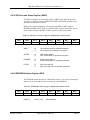
1
HighWire HW400c/2 User Reference Guide Rev 1.0
___________________HighWire HW400c/2
User Reference Guide
M8275, Rev 0.5
October 10, 2006
Copyright 2006, SBE, Inc.
Page i
HighWire HW400c/2 User Reference Guide Rev 1.0
Copyright ©2006 by SBE, Inc. All rights reserved.
No part of this manual may be reproduced by any means without written
permission from SBE, Inc., except that the purchaser may copy necessary
portions for internal use only.
While every effort has been made to ensure the accuracy of this manual, SBE
cannot be held responsible for damage resulting from information herein. All
specifications are subject to change without notice.
SBE, Inc. and the SBE logo are trademarks of SBE, Inc.
All other trademarks and copyrights are owned by their respective companies.
About SBE, Inc. SBE designs and provides IP-based networking solutions for
an extensive range of applied computing applications. SBE delivers a portfolio
of scalable, standards-based hardware and software products, including iSCSI
and VoIP, designed to enable optimal performance and rapid deployment
across a wide range of next generation communications and storage systems.
SBE is based in San Ramon, California, and can be reached at 925-355-2000
or online at http://www.sbei.com.
October 10, 2006
Copyright 2006, SBE, Inc.
Page ii
HighWire HW400c/2 User Reference Guide Rev 1.0
Revision History
Revision
1.0
October 10, 2006
Date
Changes
October 10, 2006
Initial Release
Copyright 2006, SBE, Inc.
Page iii
HighWire HW400c/2 User Reference Guide Rev 1.0
THIS PAGE IS INTENTIONALLY LEFT BLANK
October 10, 2006
Copyright 2006, SBE, Inc.
Page iv
HighWire HW400c/2 User Reference Guide Rev 1.0
Table of Contents
Revision History............................................................................................................................iii
Table of Contents .......................................................................................................................... v
List of Figures ...............................................................................................................................ix
List of Tables.................................................................................................................................ix
Conventions .................................................................................................................................xii
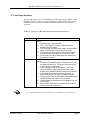
1 About This Manual...................................................................................................................... 1
2 Introduction ................................................................................................................................. 2
2.1 Product Description............................................................................................................... 2
2.2 Unpacking Instructions ......................................................................................................... 3
2.3 Handling Procedures ............................................................................................................. 4
2.4 Hardware Installation of the HW400c/2 ............................................................................... 4
2.5 Returns/Service ..................................................................................................................... 5
2.6 Operating Environment......................................................................................................... 5
2.7 Mean Time Between Failures (MTBF)................................................................................. 6
2.8 Regulatory Agency Certifications......................................................................................... 7
2.8.1 Safety........................................................................................................................... 7
2.8.2 US and Canadian Emissions........................................................................................ 7
2.8.3 European Emissions and Immunity............................................................................. 7
2.9 Agency Compliance.............................................................................................................. 7
2.10 Physical Properties.............................................................................................................. 8
2.10.1 HW400c/2 Front Panel .............................................................................................. 9
2.10.2 Part number and serial number................................................................................ 10
2.10.3 Bus Keying .............................................................................................................. 10
2.10.3.1 Compact PCI ........................................................................................................ 10
2.10.3.2 PTMC Site ............................................................................................................ 10
2.10.4 Power Requirements................................................................................................ 11
2.10.5 Switches................................................................................................................... 12
2.10.6 Product Configurations............................................................................................ 12
3 Functional Blocks ...................................................................................................................... 13
3.1 PowerPC Processor ............................................................................................................. 13
3.1.1 MPC744X Development/Debug Support.................................................................. 13
3.1.2 Console port............................................................................................................... 14
3.1.3 Pushbutton Reset / Interrupt ...................................................................................... 14
3.1.4 COP/JTAG Port......................................................................................................... 16
3.1.5 Special Purpose Jumper Block .................................................................................. 16
3.1.5.1 Jumper Pins ............................................................................................................ 17
October 10, 2006
Copyright 2006, SBE, Inc.
Page v
HighWire HW400c/2 User Reference Guide Rev 1.0
3.2 MV64462 System Controller .............................................................................................. 17
3.2.1 System Bus ................................................................................................................ 17
3.2.2 Dual Data Rate (DDR) SDRAM ............................................................................... 17
3.2.3 Host PCI Bus ............................................................................................................. 18
3.2.3.1 Operation Without CompactPCI Bus ..................................................................... 18
3.2.4 Local PCI Bus............................................................................................................ 18
3.2.5 Serial EEPROM......................................................................................................... 19
3.2.6 MV64462 Ethernet Interface ..................................................................................... 22
3.2.7 MV64462 Device Interface ....................................................................................... 22
3.2.7.1 SRAM Device ........................................................................................................ 22
3.2.7.2 Boot PROM ............................................................................................................ 22
3.2.7.3 Disk-on-Chip .......................................................................................................... 22
3.2.7.4 CT Bus Controller .................................................................................................. 23
3.2.7.5 CPLD...................................................................................................................... 23
3.2.8 Watchdog Timer........................................................................................................ 23
3.2.9 Reset .......................................................................................................................... 23
3.2.10 Multi-Purpose Port (MPP) Usage............................................................................ 24
3.3 Computer Telephony Bus Controller .................................................................................. 25
3.3.1 H.110 Interface (T8110L).......................................................................................... 25
3.3.2 T8110L Clocking Interface (T8110L)....................................................................... 25
3.3.3 Operation in Non-H.110 Backplane .......................................................................... 27
3.4 Layer 2 Ethernet Switch...................................................................................................... 27
3.4.1 Switch Registers Initialization and Monitoring......................................................... 28
3.4.2 MV64462 System Controller Ethernet Interface....................................................... 28
3.4.3 Front Panel (RJ-45) Ethernet Interface...................................................................... 28
3.4.4 PT5MC Ethernet Ports .............................................................................................. 29
3.4.5 CompactPCI Packet Switch Backplane (cPSB) Ports ............................................... 29
3.4.5.1 CompactPCI Connector J3, power and ground ...................................................... 29
3.4.6 On-board Ethernet Indicator LEDs............................................................................ 30
3.5 Mezzanine Card Sites.......................................................................................................... 32
3.5.1 PT5MC Type Mezzanine Cards ................................................................................ 32
3.5.2 PT2MC Type Mezzanine Cards ................................................................................ 32
3.5.3 PMC Type Mezzanine Cards..................................................................................... 32
3.5.4 Mezzanine Card Power.............................................................................................. 33
3.5.5 PTMC/PMC Connector Summary............................................................................. 33
3.5.6 PTMC Jn1 and Jn2 PCI Connectors .......................................................................... 34
3.5.7 PTMC Jn3 CT Bus Connector................................................................................... 35
3.5.8 PTMC Jn4 LAN/User I/O Connector........................................................................ 36
3.5.8.1 PTMC Site A Jn4.................................................................................................... 36
3.5.8.2 PTMC Site B Pn4 ................................................................................................... 38
3.5.9 PTMC Site Voltage Keying....................................................................................... 39
3.6 IPMI System Management.................................................................................................. 39
3.6.1 IPMI Controller ......................................................................................................... 39
3.6.2 Temperature and Voltage Monitor ............................................................................ 40
3.6.3 Hot Swap Ejector Latch Detection ............................................................................ 41
3.6.4 Blue (Hot Swap) LED Control .................................................................................. 41
3.6.5 Boot Status Monitor .................................................................................................. 41
3.6.6 Board Reset via IPMI ................................................................................................ 42
October 10, 2006
Copyright 2006, SBE, Inc.
Page vi
HighWire HW400c/2 User Reference Guide Rev 1.0
3.6.7 IPMI System Power Supply ...................................................................................... 42
3.6.8 IPMI Firmware EEPROMs ....................................................................................... 42
3.6.9 Zircon PM Reset........................................................................................................ 43
3.6.10 IMPI Get Device ID ................................................................................................ 43
3.7 Hot Swap Support ............................................................................................................... 44
3.7.1 Hot Swap on J1 and J2 .............................................................................................. 44
3.7.2 Hot Swap on J3.......................................................................................................... 44
3.7.3 Hot Swap on J4.......................................................................................................... 44
3.7.4 Hot Swap on J5.......................................................................................................... 44
3.7.5 Hot Swap Sequence................................................................................................... 45
4 Programming Information ......................................................................................................... 46
4.1 HW400c/2 Memory Map .................................................................................................... 46
4.2 CPLD Registers .................................................................................................................. 47
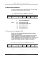
4.2.1 Clock Select Register (CSR) ..................................................................................... 48
4.2.2 Board Status Register (BSR) ..................................................................................... 49
4.2.3 LED Register A (LEDA)........................................................................................... 49
4.2.4 Memory Option Register (MOR) .............................................................................. 50
4.2.5 Geographic Addressing Register (GAR) ................................................................... 50
4.2.6 PTMC Reset Register (PRR)..................................................................................... 51
4.2.7 PTMC Control Register (PCR).................................................................................. 51
4.2.8 Board Option Register (BOR) ................................................................................... 52
4.2.9 General Purpose Register (GPR)............................................................................... 52
4.2.10 PCI Status Register (PSR) ....................................................................................... 53
4.2.11 Extended Type Register (ETR) ............................................................................... 53
4.2.12 Hardware Revision Register (HRR) ........................................................................ 54
4.2.13 PLL Configuration Register A (PLLA)................................................................... 54
4.2.14 PLL Configuration Register B (PLLB) ................................................................... 55
4.2.15 LED Register B (LEDB) ......................................................................................... 56
4.2.16 Device Control Register (DCR) .............................................................................. 57
4.2.17 CPU Timer Register (CTR)..................................................................................... 57
4.2.18 Warm Reset Register (WRR) .................................................................................. 58
4.2.19 SPI Page Register (SPR) ......................................................................................... 58
4.2.20 SPI Address Register (SAR).................................................................................... 58
4.2.21 SPI Read Byte Offset Register (SOR)..................................................................... 59
4.2.22 Read Byte Count Register (RBC)............................................................................ 59
4.2.23 Write Byte Count Register (WBC).......................................................................... 60
4.2.24 SPI Data Registers (SDR0 – SDR7)........................................................................ 60
4.2.25 SPI Error and Status Register (SESR)..................................................................... 61
4.2.26 EEPROM Address Register (EAR)......................................................................... 61
4.2.27 EEPROM Operation/Status Register (EOSR) ......................................................... 62
4.2.28 EEPROM Data Registers (EDR0 – EDR1) ............................................................. 63
4.3 Accessing the Serial EEPROM........................................................................................... 63
4.3.1 Reading an EEPROM Address.................................................................................. 63
4.3.2 Writing an EEPROM Address................................................................................... 64
4.4 Accessing the SPI Interface ................................................................................................ 64
4.4.1 Registers in the CPLD ............................................................................................... 64
4.4.2 BCM5388 Registers Access Rules ............................................................................ 64
October 10, 2006
Copyright 2006, SBE, Inc.
Page vii
HighWire HW400c/2 User Reference Guide Rev 1.0
4.4.3 Reading BCM5388 Register...................................................................................... 65
4.4.4 Writing a BCM5388 Register.................................................................................... 65
5 Linux on the HW400c/2 and Host system................................................................................. 67
5.1 Host Hardware and Software Requirements ....................................................................... 67
5.2 Network and System Configuration.................................................................................... 68
5.3 Installing Linux on your host system .................................................................................. 68
5.4 Configuring the Host System.............................................................................................. 69
5.4.1 Modifying the Host Path ........................................................................................... 69
5.4.2 Configuring the Host NFS Server ............................................................................. 69
5.4.3 Configuring Host tftp services................................................................................... 70
5.4.4 Configuring tftp with inetd ........................................................................................ 71
5.4.5 Configuring tftp with xinetd ...................................................................................... 73
5.4.6 Configuring a bootp Server ....................................................................................... 74
5.5 Booting the HW400c/2 ....................................................................................................... 75
5.5.1 U-boot, Universal Bootloader.................................................................................... 76
5.5.1.1 U-boot commands .................................................................................................. 76
5.5.1.2 U-boot environment variables ................................................................................ 77
5.5.1.3 Power up call trace ................................................................................................. 79
5.5.2 Booting with tftp........................................................................................................ 80
5.5.2.1 U-boot parameters for tftp with bootp .................................................................... 80
5.5.2.2 U-boot parameters for tftp with static IP address ................................................... 81
5.5.2.3 Boot console ........................................................................................................... 81
5.5.3 Booting with Disk on Chip........................................................................................ 84
5.5.3.1 Loading the Disk on Chip....................................................................................... 84
5.5.3.2 Creating a uRamdisk Image ................................................................................... 85
5.5.3.3 Booting from DoC .................................................................................................. 85
5.6 Compiling the Kernel (uImage) .......................................................................................... 86
5.6.1 Gentoo Application Packages Management.............................................................. 87
5.6.1.1 Emerge.................................................................................................................... 87
5.6.1.2 Enable remote login with ssh ............................................................................... 88
5.6.1.3 Starting network services; xinetd ....................................................................... 88
5.6.1.4 Starting ftp services; vsftpd ............................................................................. 88
5.7 Linux Device Drivers.......................................................................................................... 89
Appendix A IPMI GetDeviceID........................................................................................ 90
Appendix B U-Boot Environment variables...................................................................... 91
October 10, 2006
Copyright 2006, SBE, Inc.
Page viii
HighWire HW400c/2 User Reference Guide Rev 1.0
List of Figures
Figure 1. HW400c/2 Block Diagram ........................................................................................................... 3
Figure 2. The HW400c/2 PTMC Processing Platform ................................................................................ 8
Figure 3. HW400c/2 Front Panel ................................................................................................................. 9
Figure 4. Console port pin out .................................................................................................................... 14
Figure 5. J8, J9 Reset/NMI header............................................................................................................. 14
Figure 6. J8 and J9 with optional Reset/NMI cable ................................................................................... 15
Figure 7. Optional Reset/NMI switch ........................................................................................................ 16
Figure 8. COP/JTAG Pinout ...................................................................................................................... 16
Figure 9. J7 Special purpose jumper block ................................................................................................ 16
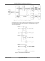
Figure 10. Local CT Bus Clocking Block Diagram................................................................................... 26
Figure 11. Local CT Bus Clock Generation .............................................................................................. 26
Figure 12. Front panel Ethernet RJ-45 LEDs ............................................................................................. 28
Figure 13. IPMI Block Diagram ................................................................................................................ 40
Figure 14. HW400c/2 Network and System environment .......................................................................... 67
List of Tables
Table 1. HW400c/2 Operating Environment ............................................................................................... 5
Table 2. HW400c/2 Physical Dimensions ................................................................................................... 8
Table 3. HW400c/2 power requirements VIO = 5.0V ............................................................................... 11
Table 4. HW400c/2 power requirements VIO = 3.3V ............................................................................... 11
Table 5. HW400c/2 Order time options...................................................................................................... 12
Table 6. HW400c/2 Processor Options...................................................................................................... 13
Table 7. J8 and J9 pin out .......................................................................................................................... 15
Table 8. J7 pin functions............................................................................................................................. 17
Table 9. Microwire EEPROM Contents, Factory Area ............................................................................. 20
Table 10. Microwire EEPROM Contents, Uboot Area............................................................................... 21
Table 11. MV64462 Multi-Purpose Port Assignments.............................................................................. 24
Table 12. LSC Assignments ...................................................................................................................... 25
Table 13. LREF [3:2] Assignments ........................................................................................................... 27
October 10, 2006
Copyright 2006, SBE, Inc.
Page ix
HighWire HW400c/2 User Reference Guide Rev 1.0
Table 14. Layer 2 Switch Port Assignments.............................................................................................. 27
Table 15. Compact PCI connector J3 pin out ............................................................................................. 30
Table 16. Mezzanine Card Power Budget ................................................................................................. 33
Table 17. PTMC/PMC Connector Summary ............................................................................................. 33
Table 18. PTMC Jn1 and Jn2 Connector Pin Assignments ....................................................................... 34
Table 19. PTMC Configuration #2/#5 Pn3 Connector Pin Assignment .................................................... 35
Table 20. PTMC Site A Configuration #2/#5 Pn4 Connector Pin Assignment......................................... 37
Table 21. PTMC Site B Configuration #2/#5 Pn4 Connector Pin Assignment ......................................... 38
Table 22. GPIO Port Assignments for IPMI.............................................................................................. 40
Table 23. Voltage Monitor A/D Port Assignments for IPMI..................................................................... 41
Table 24. HW400c/2 Temperature Sensor Locations ................................................................................ 41
Table 25. Firmware EEPROM Addresses ................................................................................................. 42
Table 26. Product ID number..................................................................................................................... 43
Table 27. Overview of Hot Swap Insertion/Extraction Sequences............................................................ 45
Table 28. HW400c/2 Memory Map........................................................................................................... 46
Table 29. CPLD Registers ......................................................................................................................... 47
Table 30. Clock Select Register (CSR) Offset Address 0x04.................................................................... 48
Table 31. Board Select Register (BSR) Offset Address 0x05 ................................................................... 49
Table 32. LED Register A (LEDA) Offset Address 0x06 ......................................................................... 49
Table 33. Memory Option Register (MOR) Offset Address 0x07............................................................. 50
Table 34. Geographic Addressing Register (CSR) Offset Address 0x08 .................................................. 50
Table 35. PTMC Reset Register (PRR) Offset Address 0x09 ................................................................... 51
Table 36. PTMC Control Register (PCR) Offset Address 0x0A ............................................................... 51
Table 37. Board Option Register (BOR) Offset Address 0x0D................................................................. 52
Table 38. General Purpose Register (GPR) Offset Address 0x0E............................................................. 52
Table 39. PCI Status Register (PSR) Offset Address 0x0F ....................................................................... 53
Table 40. Extended Type Register (ETR) Offset Address 0x10................................................................ 53
Table 41. Hardware Revision Register (HRR) Offset Address ................................................................. 54
Table 42. PLL Configuration Register A (PLLA) Offset Address 0x12 ................................................... 54
Table 43. PLL Configuration Register B (PLLB) Offset Address 0x13.................................................... 55
Table 44. LED Register B (LEDB) Offset Address 0x14.......................................................................... 56
Table 45. On-board LED functions as determined by LEDB [1:0] ........................................................... 56
Table 46. Device Control Register (CSR) Offset Address 0x15 ............................................................... 57
Table 47. CPU Timer Register (CTR) Offset Address 0x16 ..................................................................... 57
October 10, 2006
Copyright 2006, SBE, Inc.
Page x
HighWire HW400c/2 User Reference Guide Rev 1.0
Table 48. Warm Reset Register (WRR) Offset address 0x17..................................................................... 58
Table 49. SPI Page Register (SPR) Offset Address 0x1A ......................................................................... 58
Table 50. SPI Address Register (SAR) Offset Address 0x1B ................................................................... 58
Table 51. SPI Read Byte Offset Select Register (SOR) Offset Address 0x1C.......................................... 59
Table 52. Read Byte Count Register (RBC) Offset Address 0x1D ........................................................... 59
Table 53. Write Byte Count Register (WBC) Offset Address 0x1E.......................................................... 60
Table 54. SPI Data Registers (SDRn) Offset Address 0x20-0x27............................................................. 60
Table 55. SPI Error and Status Register (SESR) Offset Address 0x1F ..................................................... 61
Table 56. EEPROM Address Register (EAR) Offset Address 0x28 ......................................................... 61
Table 57. EEPROM Operation/Status Register (EOSR) Offset Address 0x29 ......................................... 62
Table 58. EEPROM Data Registers (EDRn) Offset Address 0x2A-0x2B ................................................ 63
October 10, 2006
Copyright 2006, SBE, Inc.
Page xi
HighWire HW400c/2 User Reference Guide Rev 1.0
Conventions
The following conventions are used in this document:
A # following a signal name, e.g., INTA#, represents an active low signal.
A / preceding a signal name, e.g., /INTA represents an active low signal.
0x preceding a number represents a Hexadecimal value.
A number in “ ” preceded by H represents a Hexadecimal value.
A number in “ ” preceded by B represents a Binary value.
A register or bit name that ends with _EN indicates an enable function
A register or bit name that ends with _N indicates an asserted low function
Typeface courier is used to designate code and/or terminal input.
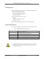
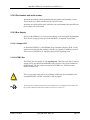
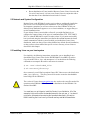
Draws attention to important information related to the nearby text.
!
October 10, 2006
Refers to information about potential hazards to equipment or personnel.
Copyright 2006, SBE, Inc.
Page xii
HighWire HW400c/2 User Reference Guide Rev 1.0
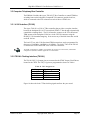
1 ABOUT THIS MANUAL
This manual is technical reference for the HighWire HW400c/2 Gigabit Switched
PTMC Processing Platform for CompactPCI. This manual is intended for those who
are installing the HW400c/2 into a system.
The HighWire HW400c/2 User Reference Manual includes the following:
• Introduction and background on the HighWire HW400c/2
• Hardware reference material
• Hardware installation instructions
• Programming information
• Physical characteristics and specifications
• Operating System Software environment and installation
October 10, 2006
Copyright 2006, SBE, Inc.
Page 1
HighWire HW400c/2 User Reference Guide Rev 1.0
2 INTRODUCTION
The HW400c/2 is a flexible high-performance core processing platform for building
powerful processor enabled CompactPCI (CPCI) telephony and data communications
I/O solutions. Advanced features on the HW400c/2 include two PCI Telecom
Mezzanine Card (PTMC) sites for CT Bus enabled I/O interfaces that are
interconnected through a high-speed Layer 2 Gigabit Ethernet switch to the dual node
CompactPCI Packet Switched Backplane (cPSB). The HighWire core architecture
utilizes the Freescale MPC7447A PowerPC processor and Marvell Discovery™ III
system controller to provide a powerful computing environment for addressing a
wide range of communications applications.
The HW400c/2 is optimized for packet-based switch fabric system architectures and
is fully compliant with the PICMG 2.16 cPSB specification. The cPSB standard
provides a switched fabric backplane interconnection using Ethernet technology
overlaid on the standard CPCI J3 connector. Dual Gigabit Ethernet interfaces are
provided on the HW400c/2 cPSB interface to support both the high availability dual
node and reduced cost single node configurations.
Full CPCI compliance and interoperability are maintained including Hot Swap,
H.110 CT Bus and rear I/O support.
2.1 Product Description
The HW400c/2 is built on SBE’s advanced HighWire core architecture, and features
the MPC7447A PowerPC processor, Marvell Discovery III system controller, up to
1GB DDR SDRAM and Disk-on-Chip flash file system storage to meet the
demanding needs of today’s telecom and datacom applications. Additional developer
features including a serial console port and a COP emulator port help speed code
development. The HW400c/2 also fully supports the Intelligent Platform
Management Interface (IPMI) standard (PICMG 2.9) for system management.
The two expansion sites accept both CT Bus enabled PTMC modules and standard
PMC modules. PT2MC modules have access to the on-board local CT Bus and
timeslot interchange fabric allowing flexible routing of TDM timeslots both between
the PTMC sites and the H.110 backplane CT Bus. PT5MC modules also include
Gigabit Ethernet connectivity to platform resources. The HW400c/2 automatically
detects each module type to provide full mix and match support for using PT2MC,
PT5MC or PMC modules in either site.
The 32-bit 33-133 MHz PCI/PCI-X interface supports 3.3V signaling modules with
full support for both front and rear I/O access per PICMG 2.3 mapping.
In addition, a 10/100/1000 Ethernet port for system management and application
flexibility is included through a front panel RJ45 connector on the board.
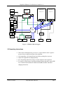
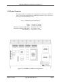
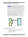
Figure 1 shows the block diagram of the HW400c/2.
October 10, 2006
Copyright 2006, SBE, Inc.
Page 2
HighWire HW400c/2 User Reference Guide Rev 1.0
Processor
Motorola
MPC7447A
SDRAM
PTMC Site A
PTMC Site B
Config #2 or #5
Config #2 or #5
SDRAM
I2C
Config.
ROM
System Controller
Discovery III
Console
RJ45
Enet
MAC
CPLD
PCI-X
TDM
GigE or
Rear I/O
PCI-X
TDM
GigE or
Rear I/O
Microwire
Serial
EEPROM
Boot
ROM
Phy
Phy
SRAM
Disk on
Chip
Enet
RJ45
Temp
Temp
Sensors
Sensors
Layer 2
Ethernet
Switch
10/100/
1000
Phy
Flash
Flash
Memor
Memory
H.110L
Controller
IPMI
Controller
Hot Swap
Controller
J1
PCI
J2
PCI-64
J3
PSB
J4
H.110
J5
Rear I/O
Figure 1. HW400c/2 Block Diagram
2.2 Unpacking Instructions
October 10, 2006
•
If the carton is damaged when you receive it, request that the carrier's agent be
present when you unpack and inspect the equipment.
•
After unpacking, verify that all items listed in the packing list are present.
•
Inspect the equipment for shipping damage.
•
Save all packing material for storage or return shipment of the equipment.
•
For repairs or replacement of equipment damaged during shipment, contact SBE,
Inc. to obtain a Return Materials Authorization (RMA) number and further
shipping instructions.
Copyright 2006, SBE, Inc.
Page 3
HighWire HW400c/2 User Reference Guide Rev 1.0
2.3 Handling Procedures
The HW400c/2 board uses CMOS components that can be easily damaged by static
electrical discharge. To avoid damage, familiarize yourself with electrostatic
discharge (ESD) procedures, which include the following precautions:
•
The board should be handled only by trained service personnel at an approved
ESD workstation.
•
Refer to ANSI/IPC-A-610 developed by the Institute for Interconnecting and
Packaging Electronic Circuits (IPC).
•
Keep the board in a sealed conductive plastic bag while in transit.
•
When installing the board in the field, ground yourself to the system chassis
before removing the board from the sealed conductive plastic bag (the power
plug must be installed on the system for this to be effective).
•
Any equipment used to work on the board must be grounded. Any person
handling the board must be grounded.
•
Check alignment and polarization of cables and connectors before applying
power.
•
Do not apply external voltages to any devices on the board with power removed
from the board.
•
Do not attempt to straighten any part soldered to the board, as pin breakage or
internal damage could occur.
2.4 Hardware Installation of the HW400c/2
The HW400c/2 is designed for use in a 6U CompactPCI enclosure.
!
October 10, 2006
Be sure to follow safe ESD procedures when handling electronic hardware.
•
Remove the HW400c/2 from the protective bag.
•
Slide the HW400c/2 into an available peripheral board slot in the CompactPCI
chassis. Check that the board is aligned properly on the card guides.
•
Completely insert the board until the top and bottom board ejectors lock into
place. If chassis power is on the blue hot swap LED will blink and turn off.
•
Tighten top and bottom screws to secure the HW400c/2 in place.
Copyright 2006, SBE, Inc.
Page 4
HighWire HW400c/2 User Reference Guide Rev 1.0
2.5 Returns/Service
Before returning any equipment for service, you must obtain a Return Material
Authorization (RMA) number from SBE:
TEL: 800-925-2666 (Toll free, USA)
TEL: +925-355-2000 (Outside of USA)
FAX: +925-355-2020
Ship all returns to SBE’s USA service center:
SBE, Inc.
4000 Executive Parkway, Suite 200
San Ramon, CA 94583
SBE’s Technical Support Department can be reached at 800-444-0990.
2.6 Operating Environment
The HW400c/2 is designed to function within the environment shown in Table 1.
Table 1. HW400c/2 Operating Environment
Storage temperature -40 to +85 C (-40 to +185 °F)
Operating temperature: 0 to 55 °C (32 to 131 °F) ambient temperature with a minimum
of 200 LFM airflow (basic configuration)
Operating humidity: 10% to 90% non-condensing
Storage humidity: 5% to 95% non-condensing
Power requirements: 36.5 Watts max. (estimated, basic configuration)
Voltages: 5V +5%/-3%, 3.3V +5%/-3%, 12V ±5% (all required)
!
October 10, 2006
Bring the HW400c/2 board to operating temperature in a non-condensing
environment. The rate of change in board temperature should not exceed
2 °C (35.6 °F) per minute.
Copyright 2006, SBE, Inc.
Page 5
HighWire HW400c/2 User Reference Guide Rev 1.0
2.7 Mean Time Between Failures (MTBF)
The Mean Time Between Failure (MTBF) of SBE, Inc’s HW400c/2 was
calculated per Telcordia Technical Reference TR-332 Issue 6, December
1997.
The following specific parameters were used:
Prediction method:
Application conditions:
Environment:
Component quality factors:
Ambient temperature:
Method I (Parts count procedure)
Case 1 (<1 hr burn-in, 50% electrical stress)
Controlled, fixed, ground (mult. factor = 1.0)
Quality level II parts (level I on Rs, Cs and LEDs)
50 C
Calculated MTBF:
>150,000 hours (not including installed PMC or PTMC modules)
October 10, 2006
Copyright 2006, SBE, Inc.
Page 6
HighWire HW400c/2 User Reference Guide Rev 1.0
2.8 Regulatory Agency Certifications
The HW400c/2 complies with the requirements listed below.
2.8.1 Safety
•
•
•
•
IEC60950
International product safety
IEC60950
UL60950
Certified Body (CB) Report
pending
pending
pending
pending
2.8.2 US and Canadian Emissions
•
•
FCC Part 15 Class B
Industry Canada CS-003
pending
pending
2.8.3 European Emissions and Immunity
•
•
EN 50082-1
pending
EN 300386-2 (supercedes EN55022)
to include EN61000-4-6: 10kHz-80MHz, 80%AM 1kHz
pending
CE Mark approval is included.
2.9 Agency Compliance
The HW400c/2 is designed to comply with the following agency requirements.
•
•
October 10, 2006
NEBS
VCC
Copyright 2006, SBE, Inc.
Page 7
HighWire HW400c/2 User Reference Guide Rev 1.0
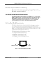
2.10 Physical Properties
The Highwire 400c/2 is compliant with the mechanical specifications of PCMIG 2.0.
Table 2 lists the physical dimensions of the HW400c/2 product. Figure 2 shows the
physical profile of the HW400c/2 board.
Table 2. HW400c/2 Physical Dimensions
Length:
Width:
Maximum component height (front):
Maximum component height (back):
Board thickness:
9.2 inches (233.68 mm)
6.3 inches (160.02 mm)
0.540 inches (13.72 mm)
0.079 inches (2 mm)
0.062 inches (1.57 mm)
Figure 2. The HW400c/2 PTMC Processing Platform
October 10, 2006
Copyright 2006, SBE, Inc.
Page 8
HighWire HW400c/2 User Reference Guide Rev 1.0
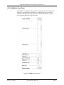
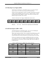
2.10.1 HW400c/2 Front Panel
The HW400c/2 CompactPCI front panel has custom cut outs with the appropriate
thickness to accommodate two PTMC bezels (with EMC gaskets), two RJ-45
connectors, blue Hot Swap LED, green power LED, and status LEDs. Figure 3
below shows an illustration of the front panel.
Figure 3. HW400c/2 Front Panel
October 10, 2006
Copyright 2006, SBE, Inc.
Page 9
HighWire HW400c/2 User Reference Guide Rev 1.0
2.10.2 Part number and serial number
All boards are marked with the manufacturing part number and assembly revision.
This is marked on a label and affixed to the top of the board.
All boards are serialized physically with a bar code serial number label and affixed to
the secondary side of the board.
2.10.3 Bus Keying
Keying on the HW400c/2 is used to prevent damage to the card and/or the backplane.
There are two keying systems used on the HW400c/2, CompactPCI and PTMC.
2.10.3.1 Compact PCI
As defined in PICMG 2.10, the HW400c/2 has a Strawberry Red key, RAL # 3018,
installed in J4 signifying the existence of the H.110 Computer Telephony bus on J4.
There is no key installed in J1, signifying universal PCI signaling levels.
2.10.3.2 PTMC Site
The PTMC Sites are capable of 3.3v signaling only. Therefore cards with 5v only IO
signals will be prevented from installation by the presence of key posts installed on
the HW400c/2. The key posts are located at each PTMC site, with the location
defined in IEEE 1386.
!
The key posts must not be removed, or damage could result from installation of an
incompatible PMC or PTMC card with 5v only IO signals.
The host PCI bus (CompactPCI) and local PCI bus (PTMC Sites) are independent of one another, and
may operate at different speeds and bus widths (see Sections 3.2.3 and 3.2.4).
October 10, 2006
Copyright 2006, SBE, Inc.
Page 10
HighWire HW400c/2 User Reference Guide Rev 1.0
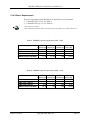
2.10.4 Power Requirements
The power requirements of the HW400c/2 are defined for two environments:
• CompactPCI VIO of 5.0v (see Table 3)
• CompactPCI VIO set 3.3v (see Table 4).
1. All voltages are required.
2. The CompactPCI VIO has no effect on the local PCI bus VIO (PTMC sites), which is fixed at 3.3v.
Table 3. HW400c/2 power requirements VIO = 5.0V
3.3V
5.0V
12V
Total
Current (A) Current (A) Current (A) Power (W)
HW400c/2 alone
PTMC site A capacity
PTMC site B capacity
HW400c/2 with PTMC A&B
2.26
4.54
4.54
11.34
6.135
2.8
2.8
11.735
0.05
0.92
0.92
1.89
38.73
40.02
40.02
118.78
Table 4. HW400c/2 power requirements VIO = 3.3V
3.3V
5.0V
12V
Total
Current (A) Current (A) Current (A) Power (W)
HW400c/2 alone
PTMC site A capacity
PTMC site B capacity
HW400c/2 with PTMC A&B
October 10, 2006
5.04
4.54
4.54
14.12
4.3
2.8
2.8
9.9
Copyright 2006, SBE, Inc.
0.05
0.92
0.92
1.89
38.73
40.02
40.02
118.78
Page 11
HighWire HW400c/2 User Reference Guide Rev 1.0
2.10.5 Switches
The HW400c/2 contains single switch that is necessary for normal operation. The
switch is an integral part of the lower ejector handle inside the front panel, and is
used along with the blue LED (see Figure 3) and the Linear Systems LTC1644, for
hot swap. The switch is connected to the PC board at J10 near the lower ejector
handle.
For debugging purposes an optional reset/NMI toggle switch and cable is available
(see Section 3.1.3). Please contact SBE Technical Support for details.
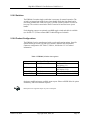
2.10.6 Product Configurations
The HW400c/2 can be manufactured with several configuration options. Specific
options include processor type and speed, memory amount, and CompactPCI
connector configuration. See Table 6, Table 16, and Section 3.2.3 for related
information.
Table 5. HW400c/2 Order time options
CPU Speed
Standard Configuration
1.0 GHz
DDR RAM
256MB
H.110 CT bus
CompactPCI bus
Installed
Installed
Options
1.4 Ghz, 1.7Ghz
(see Section 3.1)
512MB, 1GB
(see Section 3.2.2)
Uninstalled (see Section 3.3.3)
Uninstalled (See Section 3.2.3)
Options or modifications are available upon request. Please call SBE Sales for option
availability, and/or modification requests.
Build options have significant impact on power consumption.
October 10, 2006
Copyright 2006, SBE, Inc.
Page 12
HighWire HW400c/2 User Reference Guide Rev 1.0
3 FUNCTIONAL BLOCKS
The HW400c/2 has six major functional blocks – the PowerPC processor, system
controller, CT Bus interface, Ethernet switch, PTMC expansion sites, and the IPMI
controller. The following sections describe these functional blocks in greater detail.
Additional features such as the connector pin outs and JTAG development support
are also described.
3.1 PowerPC Processor
The standard configuration for the HW400c/2 includes the Freescale MPC7447A
PowerPC Processor running at 1000 MHz (1 GHz) with a corresponding system bus
speed of 166 MHz. There are two additional processor variants available for the
board, which utilize the Freescale MPC7448 PowerPC Processor with a 200 MHz
system bus speed.
The operating frequency and power consumption for each processor variant is shown
in Table 6.
Table 6. HW400c/2 Processor Options
Processor Type
Operating
Frequency
(Maximum)
System Bus
Frequency
(Maximum)
Core Power
Consumption
(Typical/Maximum)
MPC7447A
1.0 GHz
166 MHz
8.0 / 11.5 W
MPC7448
1.4 GHz
200 MHz
8.0 / 15.9 W
MPC7448
1.7 GHz
200 MHz
21 / 29.8 W
3.1.1 MPC744X Development/Debug Support
The HW400c/2 provides external access to the MPC744X processor COP port, reset
and interrupt signals at headers J6, Jx6, J7, J8, and J9 (See Figure 2). A console port
is also provided on the front panel of the board though an RJ45 modular connector
(see Figure 4, and Section 3.1.2).
October 10, 2006
Copyright 2006, SBE, Inc.
Page 13
HighWire HW400c/2 User Reference Guide Rev 1.0
3.1.2 Console port
The front panel console port is connected through the MV64462 via a Linear Systems
LTC1386 EIA-562 (low voltage EIA-232) transceiver. The console port is an RJ45
modular connector mounted on the front panel using three wire (Tx, Rx, GND) EIA232 at 9600 baud, 8N1 (8 bits, No parity, 1 stop bit). Figure 4 shows the console port
pin out.
Pin 1
1
2
3
4
5
6
7
8
n/c
n/c
Tx
Rx
CONSOLE
Shield
Figure 4. Console port pin out
3.1.3 Pushbutton Reset / Interrupt
An optional external pushbutton reset is provided as a 6-pin header (part of J8, J9, see
Figure 2, Figure 5, and Table 7) on the board that accepts the standard SBE
developer’s debug cable with toggle switch. Contact SBE Technical Support for
additional details on obtaining a developer’s debug cable.
The same toggle switch is also used to generate a non-maskable interrupt (NMI), by
pushing it in the opposite direction. The pushbutton interrupt signal is connected to a
GPIO port of the Marvell Discovery III System Controller, which can be configured
to route it to the MPC744X if desired. See Table 11 for the GPIO port number.
Indicates location of Pin 1
RST
J9
I2C2 I2C2
O NMI
J8
O
(-) SDA SCL
This row (even numbered pins)
reserved for factory use
Figure 5. J8, J9 Reset/NMI header
October 10, 2006
Copyright 2006, SBE, Inc.
Page 14
HighWire HW400c/2 User Reference Guide Rev 1.0
Table 7 describes the pin out of J8 and J9. Some of the pins listed are for Factory use
only.
Table 7. J8 and J9 pin out
Header
J8
J9
Pin
1
2
3
4
5
Label
O
SCL
none
SDA
NMI
6
1
(-)
O
2
3
none
none
4
I2C2
5
RST
6
I2C2
Usage
N/C. The “o” indicates pin one
TWSI IPMB SCL, for Factory use only
N/C. Just below the “J8” header title.
TWSI IPMB SDA, for Factory use only
Ground. Used in conjunction with J9, 1, holds
microprocessor Non Maskable Interrupt (NMI) active.
When used with optional reset/NMI cable toggles NMI.
Ground. Used with TWSI cable, for Factory use only
Non Maskable Interrupt (NMI). The “o” indicates pin
one. Used in conjunction with J8, 5, holds
microprocessor Non Maskable Interrupt (NMI) active.
N/C
Reset to the microprocessor. Used in conjunction with
J9, 5, holds microprocessor in reset. When used with
optional reset/NMI cable toggles reset line.
Select I2C2, Used with J9-6 to select I2C3 mode. For
Factory use only.
Ground. In conjunction with J9-3 to hold microprocessor
in reset.
Ground. Used with J9-4 to select I2C3 mode. For
Factory use only.
Bottom row of J8 and J9 reserved for Factory use only.
Figure 6. J8 and J9 with optional Reset/NMI cable
October 10, 2006
Copyright 2006, SBE, Inc.
Page 15
HighWire HW400c/2 User Reference Guide Rev 1.0
Figure 7. Optional Reset/NMI switch
3.1.4 COP/JTAG Port
A 16-pin header (J6, see Figure 2, and Figure 8) and a 6-pin header (JX6) are
provided on the HW400c/2 board for connecting to the processor’s COP (Common
On-chip Processor) port for factory development purposes. The J6 header can also
be used to access the JTAG chain for the entire board.
The COP/JTAG port uses 3.3V signaling.
Figure 8. COP/JTAG Pinout
3.1.5 Special Purpose Jumper Block
Jumper block J7, located along the top of the board, is used for diagnostic and other
special purposes. Under normal operating circumstances these jumpers will remain
uninstalled. The IGNP jumper is necessary when in standalone test mode (no PCI
bus is present, or no PCI Slot One Master installed). See Figure 9 and Table 8, below.
Pin 1
Figure 9. J7 Special purpose jumper block
October 10, 2006
Copyright 2006, SBE, Inc.
Page 16
HighWire HW400c/2 User Reference Guide Rev 1.0
Table 8. J7 pin functions
3.1.5.1 Jumper Label
Pins
1-2
PWR
3-4
IGNP
5-6
FAC
7-8
LPCI
9-10
IRST
11-12
IWE
13-14
ZJT
15-16
TRST
Usage
Forces board “late power” to switch “ON” at power-up
Forces board to operate as if no Host PCI bus is
present
a) Sets “FACT” bit in BSR register for use by software
b) Enables writes to Microwire EEPROM lower
addresses
Limits Local PCI bus (PTMC sites) to 100MHz
maximum frequency
Holds IPMI Controller (U92) in reset state. (Required
when programming IPMI EEPROMs on-board via the
System Controller TWSI interface, see Table 7).
Enables writes to the I2C Configuration ROM (U30)
Connects only IPMI Controller (U92) to JTAG/COP
header (J6/JX6)
Forces JTAG Reset signal inactive (Required when
using Altera ByteBlaster)
3.2 MV64462 System Controller
The HW400c/2 uses the Marvell Discovery III (MV64462) PowerPC System
Controller, which acts as the interface between the processor, memory, PCI and
device busses (see Figure 1). This section outlines the devices and functions
interfaced to the MV64462.
3.2.1 System Bus
The system bus interface between the Freescale MPC744X processor and Marvell
MV64462 system controller is a 64-bit bus, operating at a speed of 166 MHz or 200
MHz depending on the processor system bus frequency (see Table 6).
3.2.2 Dual Data Rate (DDR) SDRAM
One 200-pin SODIMM module is used for the DDR SDRAM. The module is located
under one of the PTMC mezzanine cards using a low-profile SODIMM socket.
The HW400c/2 supports DDR SDRAM densities of 256 MB, 512 MB, and 1 GB as
order time options. Memory speeds of up to 200 MHz are supported for MPC7448
processors. The memory speed is the same as the processor bus speed, and therefore
the memory speed for the standard MPC7447A (1 GHz) configuration is 166 MHz
(see Table 6).
October 10, 2006
Copyright 2006, SBE, Inc.
Page 17
HighWire HW400c/2 User Reference Guide Rev 1.0
3.2.3 Host PCI Bus
The Marvell Discovery III (MV64462) host PCI bus (PCI bus 0) provides an
interface between the processor and CompactPCI host, as well as between the PTMC
sites and the CompactPCI host. The MV64462 device acts as a PCI-to-PCI bridge
between the two PCI buses.
The HW400c/2 supports a 64-bit-wide bus operating at 33 or 66 MHz. PCI-X
operation at 66 MHz is supported; however 100/133 MHz operation is not supported.
3.2.3.1 Operation Without CompactPCI Bus
The HW400c/2 supports the PICMG 2.16 R1.0 specification’s requirement that a
PICMG 2.16 compliant node card must have the ability to operate without the
presence of the CPCI bus. CPCI connectors J1 and J2 are present as they provide
power and geographic addressing information; however pin B6 of J1 is redefined as
signal PCI_PRSNT# in PICMG 2.16. When the PCI bus is present on the backplane,
this pin is defined as GND. If the PCI bus is not present on the backplane, then it
must leave this pin floating (there is a 10K pull-up on the node).
The state of the PCI_PRSNT# signal is sensed at power-up (or hot-swap) and, if
inactive, the backplane PCI signals are ignored, enabling the board to boot up
normally. The primary PCI signals from the MV64462 are tri-stated in this case, and
the precharge voltage is switched from 1.0V to VIO (3.3V or 5V) to prevent floating
signals. The PCI Status Register (PSR) provides the status of the PCI bus (see
Section 4.2.10). The software must read this register to determine whether the PCI
bus is present or not and configure the board appropriately.
The HW400c/2 can also boot up without the slot 1 card in a CompactPCI chassis. A
jumper enables this feature, regardless of the state of the PCI_PRSNT# pin on J1.
This jumper is labeled IGNP (part of J7, see Section 3.1.5), and when installed, the
PCI reset and clock signals for MV64462 PCI bus 0 are generated internally.
!
If a Slot 1 card is present and the IGNP jumper is installed, the HW400c/2 will not be
able to communicate with the Slot 1 card.
3.2.4 Local PCI Bus
The Marvell Discovery III (MV64462) local PCI bus (PCI bus 1) provides an
interface between the processor and the two PTMC sites. The local PCI bus is 32bits wide and operates in PCI mode at 33-66 MHz, or PCI-X mode at 66-133 MHz.
The PCI-X 133 MHz speed is allowed when only one PTMC module is installed, and
it must be installed at Site B. If two PCI-X capable modules are installed, or a PCI-X
capable module is installed at Site A, the bus frequency is automatically forced to
100 MHz.
October 10, 2006
Copyright 2006, SBE, Inc.
Page 18
HighWire HW400c/2 User Reference Guide Rev 1.0
If a PCI-X 133 card is installed in Site B, it may be forced to 100 MHz, by installing the LPCI jumper at
J7 (see Section 3.1.5).
Module presence is detected by the state of the BUSMODE1 pin. Interrupts from
either of the two sites are fed through the MV64462 GPIO pins, and can be routed to
either the on-board processor or through the host PCI bus to the CompactPCI host
processor. The local PCI bus is independent of the host PCI bus, that is, the two
buses can operate at different speeds and bus widths.
!
The local PCI Bus I/O voltage is connected to 3.3 volts only. Therefore, PTMC
modules with 5-volt only I/O signals cannot be used on the HW400c/2, and are
prevented from being installed by a voltage key residing at each site (see Section
2.10.3).
3.2.5 Serial EEPROM
The HW400c/2 includes a 4 K-bit non-volatile EEPROM for storing small items such
as IP addresses and board serial numbers. This device is the Atmel AT93C66A,
which is organized in a 256 x 16-bit format. The EEPROM is accessed through
CPLD registers, which control a read/write state machine within the CPLD. See
Sections 4.2.25 to 4.2.28 for details on accessing the EEPROM.
Table 9 and Table 10 summarize the contents of the EEPROM. The first 16
addresses (0x00-0x0F) are written by SBE when the boards are manufactured, and
must not be modified. Space is reserved in the next 32 addresses (0x10-0x2F) for a
total of 16 IP Addresses, beginning with the board IP address and the Gateway IP
address. U-boot use the remaining addresses (0x30-0xFF) for boot parameters.
Boot software must read the MAC address from the serial EEPROM and subsequently assign the value
to the MV64462 Ethernet Port 0 registers. In Table 9, the MAC address is represented by the sample
number 00:A0:D6:12:34:56.
October 10, 2006
Copyright 2006, SBE, Inc.
Page 19
HighWire HW400c/2 User Reference Guide Rev 1.0
Table 9. Microwire EEPROM Contents, Factory Area
Word
Address
Bits 15-8 (MSB)
Typical
Value
Bits 7-0 (LSB)
Typical
Value
0x00
Payload Length (words)
0x20
Format
0x03
0x01
CRC32 Byte 2
0xCC
CRC32 for address 0x00
and 0x02-0x0F
0xCC
0x02
CRC32 Byte 4
0xCC
CRC32 Byte 3
0xCC
0x03
Subsystem Vendor ID
0x76
Subsystem Vendor ID
0x11
0x04
Subsystem ID
0x01
Subsystem ID
0x0D
0x05
SBE MAC Address
Header Byte 2
0xA0
SBE MAC Address
Header Byte 1
0x00
0x06
Board Serial Number
(BCD) Byte 1
0x12
SBE MAC Address
Header Byte 3
0xD6
0x07
Board Serial Number
(BCD) Byte 3
0x56
Board Serial Number
(BCD) Byte 2
0x34
0x08
Reserved
0x01
Reserved
0x43
0x09
Reserved
0x40
Reserved
0xD5
0x0A
Reserved
0x00
Reserved
0x00
0x0B
Reserved
0x00
Reserved
0x00
0x0C
Reserved
0x00
Reserved
0x00
0x0D
Reserved
0x00
Reserved
0x00
0x0E
Reserved
0x00
Reserved
0x00
0x0F
Reserved
0x00
Reserved
0x00
Shaded areas indicate addresses reserved for programming by SBE at the time the boards are
manufactured.
October 10, 2006
Copyright 2006, SBE, Inc.
Page 20
HighWire HW400c/2 User Reference Guide Rev 1.0
Table 10. Microwire EEPROM Contents, Uboot Area
Word
Address
Bits 15-8 (MSB)
Typical
Value
Bits 7-0 (LSB)
Typical
Value
0x10
Board IP Address byte 1
0xA8
Board IP Address byte 0
0xC0
0x11
Board IP Address byte 3
0x0A
Board IP Address byte 2
0x01
0x12
Gateway IP Address byte 1
0xA8
Gateway IP Address byte 0
0xC0
0x13
Gateway IP Address byte 3
0x0A
Gateway IP Address byte 2
0x01
0x14
Server IP Address byte 1
0xA8
Server IP Address byte 0
0xC0
0x15
Server IP Address byte 3
0x0A
Server IP Address byte 2
0x01
0x16 –
0x2D
Reserved for other
IP Addresses
0xFF
Reserved for other
IP Addresses
0xFF
0x2E
Netmask byte 1
0xFF
Netmask byte 0
0xFF
0x2F
Netmask byte 3
0x00
Netmask byte 2
0xFF
0x30
Baud byte 1
0x36
Baud byte 0
0x39
0x31
Baud byte 3
0x30
Baud byte 2
0x30
0x32
Baud byte 1
0x30
Baud byte 0
0x00
0x33
CRC32 byte 3
N/A
CRC32 byte 2
N/A
0x34
CRC32 byte 1
N/A
CRC32 byte 0
N/A
0x35 –
0x3A
Reserved
0xFF
Reserved
0xFF
0x3B
Load Address byte 1
Load Address byte 0
0x3C
Load Address byte 3
0x3D
Load Address byte 5
0x3E
Load Address byte 7
0x3F
Boot Delay byte 1
0xFF
0xFF
0xFF
0xFF
0x00
Boot Delay byte 0
0xFF
0xFF
0xFF
0xFF
0x35
0x40 –
0x5F
Boot Filename (32 bytes)
N/A
Boot Filename (32 bytes)
N/A
0x60 –
0xAF
Boot Arguments (80 bytes)
N/A
Boot Arguments (80 bytes)
N/A
0xB0 –
0xFF
Boot Command (80 bytes)
N/A
Boot Command (80 bytes)
N/A
Load Address byte 2
Load Address byte 4
Load Address byte 6
Addresses are typically modified by the user through the U-boot software.
October 10, 2006
Copyright 2006, SBE, Inc.
Page 21
HighWire HW400c/2 User Reference Guide Rev 1.0
3.2.6 MV64462 Ethernet Interface
The MV64462 contains an Ethernet MAC, which provides a MAC-to-MAC
connection to port 7 of the on-board Broadcom BMC5388 layer 2 Ethernet switch
(see Table 14). The connection is made via the RGMII ports on each device. The
operating speed of the RGMII port is 125 MHz.
3.2.7 MV64462 Device Interface
The Discovery III Device Interface connects the following functional elements:
•
SRAM Device
•
Boot PROM
•
Disk-on-Chip
•
CT Bus Controller
•
CPLD
The device bus is a 32-bit interface with a default operating frequency of 100 MHz.
The following sections provide additional detail for each of the functional elements.
3.2.7.1 SRAM Device
The HW400c/2 includes a 512 KB SRAM device with a 32-bit wide data bus
necessary for the processor to boot. The device supports burst reads and writes.
3.2.7.2 Boot PROM
A 4 Mbit (512 KB) Boot PROM device is supported in a PLCC socket (XU4) that is
located underneath PTMC site B. The device allows for easy upgrade of boot and/or
diagnostic code. The socket also accepts most EPROM emulator cables. Burst
reads/writes to the boot ROM are not supported.
3.2.7.3 Disk-on-Chip
A Disk-on-Chip (DoC) flash file system device is used on the HW400c/2 for data
storage. DoC is a high-density flash device manufactured by M-Systems
Incorporated, with a data bus width of 16 bits. The 128 MB device is standard on the
HW400c/2, with the option of populating other devices for OEM configurations.
Burst reads/writes to the DoC are not possible due to the maximum input clock
frequency of the device (33 MHz) being slower than the 100 MHz device bus clock.
October 10, 2006
Copyright 2006, SBE, Inc.
Page 22
HighWire HW400c/2 User Reference Guide Rev 1.0
3.2.7.4 CT Bus Controller
The Agere T8110L CT bus controller on the HW400c/2 board is accessed and
programmed via the device bus. It also has a data bus width of 16 bits. Burst
reads/writes are not supported by the T8110L. See Section 3.3 for details about the
CT Bus Controller functions.
3.2.7.5 CPLD
The Complex Programmable Logic Device (CPLD) registers are also accessed via
the device bus, using an 8-bit data bus width. Miscellaneous signals such as resets
and mezzanine card selection logic are monitored and controlled by the CPLD
registers. The CPLD supports burst reads and writes. See Section 4.2 for details
about CPLD register functions.
3.2.8 Watchdog Timer
The Marvell MV64462 Discovery III system controller contains an internal 32-bit
Watchdog Timer that can be configured as a source of interrupt to either the
MPC744X processor or to the CompactPCI host through the PCI interrupt output.
The IPMI controller can also detect a Watchdog timeout by checking the appropriate
GPIO bit (see Table 22 in Section 3.6).
3.2.9 Reset
The following types of reset are available:
•
•
•
•
•
October 10, 2006
Power–on reset. Resets the entire board during hot-swap or power-up.
Optional external pushbutton reset. See Section 3.2.9 for details.
Host PCI reset. This reset is routed through the Early Power CPLD, allowing
the host on the CompactPCI bus to reset all devices on the HW400c/2 board.
Individual device reset. The PTMC sites, the T8110L, the Ethernet Switch
and PHYs and the Disk on Chip can all be individually reset via the CPLD
register bits (see Section 4.2.16)
Software reset (warm reset). Initiated by writing to the CPLD’s Warm Reset
Register (WRR, see Section 4.2.18), resets the CPU, System Controller, and
all on board devices. Host PCI reset signal is not affected by warm reset.
Copyright 2006, SBE, Inc.
Page 23
HighWire HW400c/2 User Reference Guide Rev 1.0
3.2.10 Multi-Purpose Port (MPP) Usage
The MV64462 Discovery III includes a 32-bit Multi-Purpose Port (MPP) that can be
used for a variety of possible functions. The HW400c/2 board uses the MPP for the
serial Console Port signals (front-panel RJ-45), REQ and GNT signals for the local
PCI bus, I2C EEPROM activity indicator (used during boot*), and as a detector for
the various on-board interrupt sources.
Interrupts from the PTMC sites, the T8110L, the Ethernet PHYs, the Disk-on-Chip,
and the optional external pushbutton are connected individually to GPIO ports of the
Discovery III, which can then be configured to route them either to the MPC744X, or
to the host through the PCI interrupt output.
Table 11 lists the MV64462 MPP pin connections on the HW400c/2 board.
Table 11. MV64462 Multi-Purpose Port Assignments
MPP
Pin
MPP0
MPP1
MPP2
MPP3
MPP4
MPP5
MPP6
MPP7
MPP14
MPP15
MPP16
MPP17
MPP18
MPP19
MPP20
MPP21
MPP22
MPP23
MPP24
MPP25
MPP26
MPP27
MPP28
MPP29
MPP30
MPP31
Multiplex
Number
0x2
0x2
0x1
0x1
0x1
0x1
0x0
0x4
0x0
0x0
0x4
0x0
0x0
0x0
0x0
0x0
0x0
0x0
0x0
0x0
0x0
0x0
0x0
0x0
0x0
0x0
Pin Function
S0_TXD
S0_RXD
PCI1_GNTn[0]
PCI1_REQn[0]
PCI1_GNTn[1]
PCI1_REQn[1]
GPIO6
INITACT
GPIO14
GPIO15
WD_NMIn
GPIO17
GPIO18
GPIO19
GPIO20
GPIO21
GPIO22
GPIO23
GPIO24
GPIO25
GPIO26
GPIO27
GPIO28
GPIO29
GPIO30
GPIO31
In/Out of
Disco III
Out
In
Out
In
Out
In
Out
Out
In
In
Out
In
In
In
In
In
In
In
In
In
In
In
In
In
In
In
Active
High/Low
High
High
Low
Low
Low
Low
Low
High
Low
Low
Low
Low
Low
Low
Low
Low
Low
Low
Low
High
High
Low
Low
Low
Low
Low
Signal Description
Console Port (RJ-45) TXD
Console Port (RJ-45) RXD
GNT to PTMC Site A
REQ from PTMC Site A
GNT to PTMC Site B
REQ from PTMC Site B
Disk-on-Chip Lock
I2C EEPROM Active*
Pushbutton Interrupt
CPU Temp Sensor TCRIT
Watchdog Signal to IPMI
INTA from PTMC site A
INTB from PTMC site A
INTC from PTMC site A
INTD from PTMC site A
INTA from PTMC site B
INTB from PTMC site B
INTC from PTMC site B
INTD from PTMC site B
T8110L Clock Error
T8110L System Error
PHY A Interrupt
PHY B Interrupt
PHY R Interrupt (RJ-45)
Disk-on-Chip Interrupt
Disk-on-Chip Busy Signal
* By default, the HW400c/2 uses the I2C EEPROM during boot. The EEPROM
must contain the appropriate register setting to configure MPP7 as the INITACT
output. This signal is then pulled low after the EEPROM loads to initiate the
processor boot
October 10, 2006
Copyright 2006, SBE, Inc.
Page 24
HighWire HW400c/2 User Reference Guide Rev 1.0
3.3 Computer Telephony Bus Controller
The HW400c/2 includes the Agere T8110L CT Bus Controller to control TDM bus
switching between the backplane (CompactPCI J4 connector) and the local bus,
which is connected to the JN3 connector on each of the two PTMC sites.
3.3.1 H.110 Interface (T8110L)
The Agere T8110L is a H.110 CT Bus controller that provides a complete interface
between the backplane H.110 CT bus and local PTMC CT bus through a dynamically
controllable switching fabric. The H.110 interface connects to all 32 bi-directional
TDM streams of the backplane H.110 bus via the CPCI J4 connector using the
PICMG 2.5 R1.0 standard mapping. It can access any of the 4096 time slots carried
on the H.110 bus.
The local CT bus, with 32 bi-directional TDM connections, can be programmed for
data rates of 2.048Mb/s, 4.092Mb/s or 8.192Mb/s. The local CT bus of the T8110L
is connected to each of the PTMC sites via the JN3 connectors.
The PTMC configuration 2 (PT2MC) type modules only support 20 CT bus streams, while PTMC
configuration 5 (PT5MC) modules support all 32 CT bus streams.
3.3.2 T8110L Clocking Interface (T8110L)
The T8110L LSC [3:0] output pins are connected to the PTMC Output Clock Drivers
located in the CPLD. The LSC[3:0] pins are programmed as shown in Table 6.
Table 12. LSC Assignments
LSC output
LSC0
LSC1
LSC2
LSC3
Signal Assignment
CT_C8
CT Frame
NETREF1
NETREF2
Figure 10 shows the local CT Bus clocking signals and how they are routed.
October 10, 2006
Copyright 2006, SBE, Inc.
Page 25
HighWire HW400c/2 User Reference Guide Rev 1.0
Figure 10. Local CT Bus Clocking Block Diagram
Control for the local “A” and “B” bus drivers is provided by bits 4, 5, 6, and 7 in the
Clock Select Register (CSR). Refer to Section 4.2.1 for further details. Figure 11
shows the implementation.
Figure 11. Local CT Bus Clock Generation
October 10, 2006
Copyright 2006, SBE, Inc.
Page 26
HighWire HW400c/2 User Reference Guide Rev 1.0
The T8110L can be programmed such that its local frame reference (LREF [3:2])
inputs are used to generate all of the TDM bus clocks and syncs. The T8110L Local
Clock Reference Inputs have been assigned to the PTMC JN3 H.110 clock pins as
shown in Table 13.
Table 13. LREF [3:2] Assignments
LREF input
LREF2
LREF3
Assigned to Clock
PT_NETREF1
PT_NETREF2
3.3.3 Operation in Non-H.110 Backplane
The default HW400c/2 configuration has the H.110 interface installed. However, in
the event that the HW400c/2 board is used in a PICMG 2.16 chassis that does not
have an H.110 bus or the H.110 interface is not installed, the CT_EN pin on J4 (pin
C23) is not grounded. The state of the CT_EN pin is stored in bit 7 of the CPLD
BSR register for access by software (see 4.2.2). If H.110 is not present, the H.110
interface should not be enabled.
Even if the H.110 bus is not available on the CompactPCI backplane, the local CT
Bus connections are still valid and therefore PTMC Site A and PTMC Site B can
communicate via the CT Bus that is local to the HW400c/2 board.
3.4 Layer 2 Ethernet Switch
The Broadcom BCM5388 Layer 2 Ethernet switch connects to the various devices on
the HW400c/2 board. The BCM5388 has four Gigabit Ethernet ports with integral
MAC/PHYs, and four additional Gigabit MACs with external RGMII connections.
Three of the additional MACs are connected to Broadcom BCM5461S external
PHYs, and one is connected directly to the MV64462 MAC port as shown in Table
14.
Table 14. Layer 2 Switch Port Assignments
Switch Port
7
6
2
4
3
5
0
1
October 10, 2006
Device or Port
MV64462 System Controller
Front Panel RJ-45
PT5MC Slot A, Link Port A
PT5MC Slot A, Link Port B
PT5MC Slot B, Link Port A
PT5MC Slot B, Link Port B
PSB Link Port A
PSB Link Port B
PHY Address
N/A
00110
N/A
00100
N/A
00101
N/A
N/A
Copyright 2006, SBE, Inc.
Connection Type
MAC-to-MAC RGMII
1 External PHY
1 Integral PHY
1 External PHY
1 Integral PHY
1 External PHY
1 Integral PHY
1 Integral PHY
Page 27
HighWire HW400c/2 User Reference Guide Rev 1.0
3.4.1 Switch Registers Initialization and Monitoring
The switch is initialized and its registers polled by utilizing its SPI bus interface.
This interface is connected through the CPLD. For a description of how to access the
SPI interface, please refer to Section 4.4.
3.4.2 MV64462 System Controller Ethernet Interface
The Marvell MV64462 System Controller on the HW400c/2 can be accessed via the
BCM5388 Ethernet switch. The connection speed must be set to 1000 Mbps and is a
MAC-to-MAC connection with the clock sourced from the Ethernet switch. The
transmitter signals from the switch are connected to the receiver signals on the
system controller, and vice-versa for a direct MAC-to-MAC connection.
3.4.3 Front Panel (RJ-45) Ethernet Interface
The HW400c/2 board includes a fully shielded RJ-45 (with integrated transformer
and two green LEDs) located at the front panel that provides an Ethernet LAN
interface. The port is auto-negotiating and auto-sensing, and operates at 10/100/1000
Mbps. The left LED (looking at the port) indicates Link/Activity/Speed and the right
LED indicates collision detection (See Figure 12).
The Link/Activity/Speed LED indication is as follows:
•
solid green when the network link is up;
•
blinking at 3 Hz for 10 Mb/s Tx or Rx;
•
blinking at 6 Hz for 100 Mb/s Tx or Rx;
•
and blinking at 12 Hz for 1000 Mb/s Tx or Rx.
Link/activity/speed
Collision
Ethernet
Figure 12. Front panel Ethernet RJ-45 LEDs
October 10, 2006
Copyright 2006, SBE, Inc.
Page 28
HighWire HW400c/2 User Reference Guide Rev 1.0
3.4.4 PT5MC Ethernet Ports
Each of the two PT5MC sites on the HW400c/2 have two 10/100/1000 Mbps ports
connected to the Ethernet switch. The signals conform to PICMG ECN 2.15-1.0001, using the first 24 pins of the respective JN4 connectors.
The JN4 Ethernet connections are switched to the CompactPCI J3 connector using a
FET switch specially designed for signals such as Gigabit Ethernet. The PTID bits
control the FET, when a PT5MC module is installed in either mezzanine card site.
Should a non-PT5MC module be installed in one of the sites, the JN4 signals for that
site are routed to the CompactPCI J5 connector as user I/O according to PICMG 2.3
R1.0.
!
JN4 pins 5, 6, 11, 12, 17, 18, 23 and 24 are switched to ground through discrete FETs
at the JN4 connector when a PT5MC module is installed. This has the effect of
grounding the respective connections at the CompactPCI J5 connector as well, so
caution must be exercised not to damage circuitry on an installed RTM.
!
PT5MC cards with network connections through Pn4, must be transformer coupled or
the link to the layer 2 switch will not be established.
3.4.5 CompactPCI Packet Switch Backplane (cPSB) Ports
Two of the 10/100/1000BaseT ports of the Ethernet switch, Port 0 and Port 1, are
routed to the CompactPCI J3 connector as specified for Packet Switching Backplane
(PSB) in PICMG 2.16. See Table 14 and Table 15. The HW400c/2 is configured as a
PCIG 2.16 Node card.
3.4.5.1 CompactPCI Connector J3, power and ground
!
October 10, 2006
The HW400c/2 uses some of the J3 pins, designated by the PICMG 2.16 as User I/O,
as power and ground pins in order to provide enough current to handle some of the
more power hungry PTMC cards. These power pins cannot be disconnected. This can
damage to some Rear Transition Modules (RTM). The SBE assigned power and
ground pins are shown in bold in Table 15.
Copyright 2006, SBE, Inc.
Page 29
HighWire HW400c/2 User Reference Guide Rev 1.0
Table 15. Compact PCI connector J3 pin out
1
2
3
4
5
6
7
8
9
10
11
12
13
14
15
16
17
18
19
A
+5.0v
+5.0v
N/C
LED Clock
N/C
LED Data
N/C
+3.3v
+3.3v
+3.3v
N/C
N/C
N/C
GND
LPb DB+
LPb DA+
LPa DB+
LPa DA+
GND
B
+5.0v
+12v
N/C
N/C
N/C
N/C
N/C
N/C
N/C
N/C
GND
N/C
N/C
GND
LPb DBLPb DALPa DBLPa DAGND
C
N/C
N/C
N/C
N/C
N/C
N/C
N/C
GND
N/C
N/C
GND
N/C
N/C
GND
GND
GND
GND
GND
GND
D
N/C
N/C
N/C
N/C
N/C
N/C
N/C
GND
N/C
N/C
N/C
N/C
N/C
GND
LPb DD+
LPb DC+
LPa DD+
LPa DC+
GND
E
N/C
N/C
N/C
N/C
N/C
GND
N/C
N/C
GND
N/C
N/C
N/C
N/C
GND
LPb DDLPb DCLPa DDLPa DCGND
3.4.6 On-board Ethernet Indicator LEDs
The HW400c/2 includes eight on-board LEDs for monitoring the status of the various
Ethernet ports. The LEDs are labeled L0-L8 and are located near CompactPCI
connector J5.
The BCM5388 has a serial LED interface, from which the status of all eight ports can
be extracted. The serial LED signal is routed to the CPLD, which contains a state
machine that decodes the LED states for each port. The eight status LEDs on the top
edge of the HW400c/2 board can be configured to show the status for all eight
Ethernet ports. Each status LED gives the status for its corresponding port in the
Link/Activity/Speed format. The CPLD LED registers control the selection of
Ethernet status, boot status, or general debug modes for the eight LEDs.
The serial LED interface signals are also routed to the RTM through CompactPCI
connector J3.
LEDMODE settings on the BCM5388 are hardwired to “101” (see Serial LED Interface section in the
BCM5388 datasheet).
October 10, 2006
Copyright 2006, SBE, Inc.
Page 30
HighWire HW400c/2 User Reference Guide Rev 1.0
The Link/Activity/Speed LED indication is as follows:
•
solid green when the network link is up
•
blinking at 3 Hz for 10 Mb/s Tx or Rx;
•
blinking at 6 Hz for 100 Mb/s Tx or Rx;
•
blinking at 12 Hz for 1000 Mb/s Tx or Rx.
An optional front panel 2-high LED is provided as a status indicator for the Ethernet
ports. The optional LEDs are shown as LEDs C and D in Figure 3, and by default are
not present. The left LED indicates Link/Activity/Speed and the right LED indicates
Collision detection for the selected port. A port is selected by setting the appropriate
CPLD bit. The default selection (when present) is the Marvell MV64462 System
Controller MAC.
See Section 4.2 for details on setting the LED modes.
October 10, 2006
Copyright 2006, SBE, Inc.
Page 31
HighWire HW400c/2 User Reference Guide Rev 1.0
3.5 Mezzanine Card Sites
The HW400c/2 board supports I/O expansion using either one or two industrystandard PTMC and/or PMC modules. This section provides technical details for
these expansion sites.
3.5.1 PT5MC Type Mezzanine Cards
The PT5MC mezzanine card support includes connection to the local PCI bus (32-bit,
33-133 MHz PCI or PCI-X), the local 32 TDM stream H.110 bus, two Gigabit
Ethernet ports, and 31 pins of User I/O connected to the CompactPCI J5 backplane
connector.
!
PT5MC cards with network connections through Pn4, must be transformer coupled or
the link to the layer 2 switch will not be established.
3.5.2 PT2MC Type Mezzanine Cards
The PT2MC mezzanine card support includes connection to the local PCI bus (32-bit,
33-133 MHz PCI or PCI-X), the local 20 TDM stream H.110 bus, and 55 pins of
User I/O connected to the CompactPCI J5 backplane connector. RMII signals are not
supported, therefore these lines cannot be used by the PT2MC cards.
3.5.3 PMC Type Mezzanine Cards
The PMC mezzanine card support includes connection to the local PCI bus (32-bit,
33-133 MHz PCI or PCI-X), and 55 pins of User I/O connected to the CompactPCI
J5 backplane connector.
PMC cards have specified Jn3 as user defined I/O or 64 bit PCI. However, on the HW400c/2, these lines
are assigned only to the CT bus and RGMII bus, so when a PMC card is installed the signals on Jn3 are
tri-stated (see Table 17).
October 10, 2006
Copyright 2006, SBE, Inc.
Page 32
HighWire HW400c/2 User Reference Guide Rev 1.0
3.5.4 Mezzanine Card Power
Each of the two mezzanine card sites on the HW400c/2 is allotted a portion of the
total power budget for the board. For the standard version, the mezzanine power
budget is 16.2 Watts for each slot, while the optional high-power version allows 26.4
Watts for each slot. The power budget is divided between the 3.3V, 5V, and 12V
power rails as shown in Table 16.
Table 16. Mezzanine Card Power Budget
Power (per site)
HW400c/2
Version
Mezzanine Card
Total Power
(per site)
3.3V power
(Per slot)
5V power
(Per slot)
12V power
(Per slot)
Standard
without J4
16.2 Watts
10 Watts
5 Watts
1.2 Watts
Standard
with J4
29.4 Watts
15 Watts
12 Watts
2.4 Watts
Optional High
Power with J4
26.4 Watts
16.5 Watts
7.5 Watts
2.4 Watts
The standard version with additional power supplied from the CompactPCI J4
connector yields the highest power rating for the mezzanine card slots, because that
version has a lower power processor than the optional high-power version.
3.5.5 PTMC/PMC Connector Summary
Table 17 summarizes the mezzanine card connections for each supported type. Both
sites A and B support the same array of connections. Connector pin outs are shown in
Sections 3.5.6, 3.5.7, and 3.5.8
Table 17. PTMC/PMC Connector Summary
Mezzanine
Card Type
JN1/JN2
JN3
JN4
PMC
PCI or
PCI-X
Not Used (tri-stated)
55 Pins User I/O
PT2MC
PCI or
PCI-X
Local CT Bus
(20-bit)
55 Pins User I/O
PT5MC
PCI or
PCI-X
Local CT Bus
(32-bit)
2 LAN Ports
31 Pins User I/O
October 10, 2006
Copyright 2006, SBE, Inc.
Page 33
HighWire HW400c/2 User Reference Guide Rev 1.0
3.5.6 PTMC Jn1 and Jn2 PCI Connectors
Communication using the local PCI bus is done across two PTMC/PMC connectors,
JN1 and JN2. Table 18 shows the 32-bit PCI connector pin assignment for JN1 and
JN2 on the HW400c/2 as defined by the PMC specification IEEE P1386.1.
Table 18. PTMC Jn1 and Jn2 Connector Pin Assignments
Pn1 32-Bit PCI
Pin
#
Pn2 32-Bit PCI
Pin
#
Pin
#
Signal Name
Signal Name
1
TCK
-12V
2
3
Ground
INTA#
4
5
INTB#
INTC#
7
BUSMODE1#
9
Pin
#
Signal Name
Signal Name
1
+12V
TRST#
2
3
TMS
TDO
4
6
5
TDI
Ground
6
+5V
8
7
Ground
PCI-RSVD*
8
INTD#
PCI-RSVD*
10
9
PCI-RSVD*
PCI-RSVD*
10
11
Ground
3.3Vaux
12
11
BUSMODE2#
+3.3V
12
13
CLK
Ground
14
13
RST#
BUSMODE3#
14
15
Ground
GNT#
16
15
+3.3V
BUSMODE4#
16
17
REQ#
+5V
18
17
PME#
Ground
18
19
V (I/O)
AD[31]
20
19
AD[30]
AD[29]
20
21
AD[28]
AD[27]
22
21
Ground
AD[26]
22
23
AD[25]
Ground
24
23
AD[24]
+3.3V
24
25
Ground
C/BE[3]#
26
25
IDSEL
AD[23]
26
27
AD[22]
AD[21]
28
27
+3.3V
AD[20]
28
29
AD[19]
+5V
30
29
AD[18]
Ground
30
31
V (I/O)
AD[17]
32
31
AD[16]
C/BE[2]#
32
33
FRAME#
Ground
34
33
Ground
PMC-RSVD
34
35
Ground
IRDY#
36
35
TRDY#
+3.3V
36
37
DEVSEL#
+5V
38
37
Ground
STOP#
38
39
Ground
LOCK#
40
39
PERR#
Ground
40
41
PCI-RSDV*
PCI-RSVD*
42
41
+3.3V
SERR#
42
43
PAR
Ground
44
43
C/BE[1]#
Ground
44
45
V (I/O)
AD[15]
46
45
AD[14]
AD[13]
46
47
AD[12]
AD[11]
48
47
M66EN
AD[10]
48
49
AD[09]
+5V
50
49
AD[08]
+3.3V
50
51
Ground
C/BE[0]#
52
51
AD[07]
PMC-RSVD
52
53
AD[06]
AD[05]
54
53
+3.3V
PMC-RSVD
54
55
AD[04]
Ground
56
55
PMC-RSVD
Ground
56
57
V (I/O)
AD[03]
58
57
PMC-RSVD
PMC-RSVD
58
59
AD[02]
AD[01]
60
59
Ground
PMC-RSVD
60
61
AD[00]
+5V
62
61
ACK64#
+3.3V
62
63
Ground
REQ64#
64
63
Ground
PMC-RSVD
64
October 10, 2006
Copyright 2006, SBE, Inc.
Page 34
HighWire HW400c/2 User Reference Guide Rev 1.0
3.5.7 PTMC Jn3 CT Bus Connector
Table 19 shows the PTMC Pn3 CT Bus connector pin assignment for the HW400c/2
for both Configuration #2 (PT2MC) and Configuration #5 (PT5MC). The signal
definitions for Pn3 are per the PICMG 2.15 specification.
Table 19. PTMC Configuration #2/#5 Pn3 Connector Pin Assignment
Pn3 PT2MC
Pin
#
Signal Name
1
3
Pn3 PT5MC
Signal Name
Pin
#
Pin
#
Signal Name
Signal Name
Pin
#
Hi Z
Ground
2
1
LCT D26
Ground
2
Ground
STX (N/C)
4
3
Ground
STX (N/C)
4
5
Hi Z
SRX (N/C)
6
5
LCT D24
SRX (N/C)
6
7
Hi Z
Ground
8
7
LCT D22
Ground
8
9
PTID2
Hi Z
10
9
PTID2
LCT D31
10
11
PTGNDZ
Hi Z
12
11
PTGNDZ
LCT D29
12
13
Hi Z
Ground
14
13
LCT D20
Ground
14
15
Ground
Hi Z
16
15
Ground
LCT D27
16
17
LCT FA
Hi Z
18
17
LCT FA
LCT D25
18
19
LCT FB
Ground
20
19
LCT FB
Ground
20
21
PTID0
Hi Z
22
21
PTID0
LCT D23
22
23
PTGNDZ
Hi Z
24
23
PTGNDZ
LCT D21
24
25
LCT C8A
Ground
26
25
LCT C8A
Ground
26
27
Ground
LCT D19
28
27
Ground
LCT D19
28
29
LCT D18
LCT D17
30
29
LCT D18
LCT D17
30
31
LCT D16
Ground
32
31
LCT D16
Ground
32
33
Ground
NETREF2
34
33
Ground
NETREF2
34
35
LCT D14
Hi Z
36
35
LCT D14
LCT D30
36
37
LCT D12
Ground
38
37
LCT D12
Ground
38
39
PTENB#
Hi Z
40
39
PTENB#
LCT D28
40
41
PTGNDZ
NETREF1
42
41
PTGNDZ
NETREF2
42
43
LCT C8B
Ground
44
43
LCT C8B
Ground
44
45
Ground
LCT D15
46
45
Ground
LCT D15
46
47
LCT D10
LCT D13
48
47
LCT D10
LCT D13
48
49
LCT D8
LCT D11
50
49
LCT D8
LCT D11
50
51
Ground
LCT D9
52
51
Ground
LCT D9
52
53
LCT D6
LCT D7
54
53
LCT D6
LCT D7
54
55
LCT D4
Ground
56
55
LCT D4
Ground
56
57
PTID1
LCT D5
58
57
PTID1
LCT D5
58
59
LCT D2
LCT D3
60
59
LCT D2
LCT D3
60
61
LCT D0
Ground
62
61
LCT D0
Ground
62
63
Ground
LCT D1
64
63
Ground
LCT D1
64
For PT2MC cards, the PT2MC MII signals are tri-stated (Hi Z), as they are hard wired to the CTbus for
PT5MC use.
PTMC Serial Port signals (STX and SRX) are not connected on the HW400c/2.
October 10, 2006
Copyright 2006, SBE, Inc.
Page 35
HighWire HW400c/2 User Reference Guide Rev 1.0
3.5.8 PTMC Jn4 LAN/User I/O Connector
Table 20 (Site A) and Table 21 (Site B) show the PTMC Pn4 LAN and/or User I/O
connector pin assignment for the HW400c/2 for both Configuration #2 (PT2MC User
I/O only) and Configuration #5 (PT5MC LAN and User I/O).
3.5.8.1 PTMC Site A Jn4
This table shows the connections from PTMC Site A Jn4, to the Compact PCI
connector J5 and, for PT5MC, the signals for the Ethernet ports, Link Ports A and B.
LPa (Link Port A) and LPb (Link Port B) for PTMC Site A go to the Ethernet Switch ports 2 and 4
respectively. See Table 14.
!
October 10, 2006
PT5MC cards with network connections through Pn4, must be transformer coupled or
the link to the layer 2 switch will not be established.
Copyright 2006, SBE, Inc.
Page 36
HighWire HW400c/2 User Reference Guide Rev 1.0
Table 20. PTMC Site A Configuration #2/#5 Pn4 Connector Pin Assignment
Pn4 PT2MC
Pin
#
Signal Name
1
3
Pn4 PT5MC
Signal Name
Pin
#
Pin
#
Signal Name
Signal Name
Pin
#
cPCI J5 E22
cPCI J5 D22
2
1
LPa DA+
LPa DC+
2
cPCI J5 C22
cPCI J5 B22
4
3
LPa DA-
LPa DC-
4
5
cPCI J5 A22
cPCI J5 E21
6
5
Ground
Ground
6
7
cPCI J5 D21
cPCI J5 C21
8
7
LPa DB+
LPa DD+
8
9
cPCI J5 B21
cPCI J5 A21
10
9
LPa DB-
LPa DD-
10
11
cPCI J5 E20
cPCI J5 D20
12
11
Ground
Ground
12
13
cPCI J5 C20
cPCI J5 B20
14
13
LPb DA+
LPb DC+
14
15
cPCI J5 A20
cPCI J5 E19
16
15
LPb DA-
LPb DC-
16
17
cPCI J5 D19
cPCI J5 C19
18
17
Ground
Ground
18
19
cPCI J5 B19
cPCI J5 A19
20
19
LPb DB+
LPb DD+
20
21
cPCI J5 E18
cPCI J5 D18
22
21
LPb DB-
LPb DD-
22
23
cPCI J5 C18
cPCI J5 B18
24
23
Ground
Ground
24
25
cPCI J5 A18
cPCI J5 E17
26
25
cPCI J5 A18
cPCI J5 E17
26
27
cPCI J5 D17
cPCI J5 C17
28
27
cPCI J5 D17
cPCI J5 C17
28
29
cPCI J5 B17
cPCI J5 A17
30
29
cPCI J5 B17
cPCI J5 A17
30
31
cPCI J5 E16
cPCI J5 D16
32
31
cPCI J5 E16
cPCI J5 D16
32
33
cPCI J5 C16
cPCI J5 B16
34
33
cPCI J5 C16
cPCI J5 B16
34
35
cPCI J5 A16
cPCI J5 E15
36
35
cPCI J5 A16
cPCI J5 E15
36
37
cPCI J5 D15
cPCI J5 C15
38
37
cPCI J5 D15
cPCI J5 C15
38
39
cPCI J5 B15
cPCI J5 A15
40
39
cPCI J5 B15
cPCI J5 A15
40
41
cPCI J5 E14
cPCI J5 D14
42
41
cPCI J5 E14
cPCI J5 D14
42
43
cPCI J5 C14
cPCI J5 B14
44
43
cPCI J5 C14
cPCI J5 B14
44
45
cPCI J5 A14
cPCI J5 E13
46
45
cPCI J5 A14
cPCI J5 E13
46
47
cPCI J5 D13
cPCI J5 C13
48
47
cPCI J5 D13
cPCI J5 C13
48
49
cPCI J5 B13
cPCI J5 A13
50
49
cPCI J5 B13
cPCI J5 A13
50
51
cPCI J5 E12
cPCI J5 D12
52
51
cPCI J5 E12
cPCI J5 D12
52
53
cPCI J5 C12
cPCI J5 B12
54
53
cPCI J5 C12
cPCI J5 B12
54
55
cPCI J5 A12
N/C
56
55
cPCI J5 A12
N/C
56
57
N/C
N/C
58
57
N/C
N/C
58
59
N/C
N/C
60
59
N/C
N/C
60
61
N/C
N/C
62
61
N/C
N/C
62
63
N/C
N/C
64
63
N/C
N/C
64
October 10, 2006
Copyright 2006, SBE, Inc.
Page 37
HighWire HW400c/2 User Reference Guide Rev 1.0
3.5.8.2 PTMC Site B Pn4
This table shows the connections from PTMC Site B Jn4 to the Compact PCI
connector J5 and, for PT5MC, the signals for the Ethernet ports, Link Ports A and B.
LPa (Link Port A) and LPb (Link Port B) for PTMC Site A go to the Ethernet Switch ports 3 and 5
respectively. See Table 14.
PT5MC cards with network connections through Pn4, must be transformer coupled or
the link to the layer 2 switch will not be established.
!
Table 21. PTMC Site B Configuration #2/#5 Pn4 Connector Pin Assignment
Pn4 PT2MC
Pn4 PT5MC
Signal Name
Pin
#
Pin
#
Signal Name
Signal Name
Pin
#
cPCI J5 E11
cPCI J5 D11
2
1
LPa DA+
LPa DC+
2
cPCI J5 C11
cPCI J5 B11
4
3
LPa DA-
LPa DC-
4
5
cPCI J5 A11
cPCI J5 E10
6
5
Ground
Ground
6
7
cPCI J5 D10
cPCI J5 C10
8
7
LPa DB+
LPa DD+
8
9
cPCI J5 B10
cPCI J5 A10
10
9
LPa DB-
LPa DD-
10
11
cPCI J5 E9
cPCI J5 D9
12
11
Ground
Ground
12
13
cPCI J5 C9
cPCI J5 B9
14
13
LPb DA+
LPb DC+
14
15
cPCI J5 A9
cPCI J5 E8
16
15
LPb DA-
LPb DC-
16
17
cPCI J5 D8
cPCI J5 C8
18
17
Ground
Ground
18
19
cPCI J5 B8
cPCI J5 A8
20
19
LPb DB+
LPb DD+
20
21
cPCI J5 E7
cPCI J5 D7
22
21
LPb DB-
LPb DD-
22
23
cPCI J5 C7
cPCI J5 B7
24
23
Ground
Ground
24
25
cPCI J5 A7
cPCI J5 E6
26
25
cPCI J5 A7
cPCI J5 E6
26
27
cPCI J5 D6
cPCI J5 C6
28
27
cPCI J5 D6
cPCI J5 C6
28
29
cPCI J5 B6
cPCI J5 A6
30
29
cPCI J5 B6
cPCI J5 A6
30
31
cPCI J5 E5
cPCI J5 D5
32
31
cPCI J5 E5
cPCI J5 D5
32
33
cPCI J5 C5
cPCI J5 B5
34
33
cPCI J5 C5
cPCI J5 B5
34
35
cPCI J5 A5
cPCI J5 E4
36
35
cPCI J5 A5
cPCI J5 E4
36
37
cPCI J5 D4
cPCI J5 C4
38
37
cPCI J5 D4
cPCI J5 C4
38
39
cPCI J5 B4
cPCI J5 A4
40
39
cPCI J5 B4
cPCI J5 A4
40
41
cPCI J5 E3
cPCI J5 D3
42
41
cPCI J5 E3
cPCI J5 D3
42
43
cPCI J5 C3
cPCI J5 B3
44
43
cPCI J5 C3
cPCI J5 B3
44
45
cPCI J5 A3
cPCI J5 E2
46
45
cPCI J5 A3
cPCI J5 E2
46
47
cPCI J5 D2
cPCI J5 C2
48
47
cPCI J5 D2
cPCI J5 C2
48
49
cPCI J5 B2
cPCI J5 A2
50
49
cPCI J5 B2
cPCI J5 A2
50
51
cPCI J5 E1
cPCI J5 D1
52
51
cPCI J5 E1
cPCI J5 D1
52
53
cPCI J5 C1
cPCI J5 B1
54
53
cPCI J5 C1
cPCI J5 B1
54
55
CPCIJ5 A1
N/C
56
55
cPCI J5 A1
N/C
56
57
N/C
N/C
58
57
N/C
N/C
58
59
N/C
N/C
60
59
N/C
N/C
60
61
N/C
N/C
62
61
N/C
N/C
62
63
N/C
N/C
64
63
N/C
N/C
64
Pin
#
Signal Name
1
3
October 10, 2006
Copyright 2006, SBE, Inc.
Page 38
HighWire HW400c/2 User Reference Guide Rev 1.0
3.5.9 PTMC Site Voltage Keying
Voltage key posts are installed at each PTMC site in accordance with IEEE 1386. See
Section 2.10.3.
!
The HW400c/2 local PCI bus I/O voltage is 3.3 volts only. Therefore, PTMC and
PMC modules with 5 volt only I/O signals cannot be used on the HW400c/2
board, and are prevented from being installed by a key post residing at each site.
3.6 IPMI System Management
The HW400c/2 board includes an IPMI controller that interfaces to the System
Management Bus (SMB) as defined by the PICMG 2.9 specification. The IPMI
information is only accessible through an IPMI Shelf Manager, and is used to
monitor and report the health of the HW400c/2.
An IPMI Shelf manager may not be present in the system, and IPMI may, in fact, not even have power.
In either case, the IPMI circuitry on board is for monitoring purposes only and, if disabled or not used,
has no affect the normal operation of the HW400c/2.
3.6.1 IPMI Controller
The IPMI controller on the HW400c/2 is the QLogic Zircon PM with board-specific
firmware. The Zircon PM complies with PICMG hot-swap requirements.
The Zircon PM communicates with the System Management device (residing on the
slot 0 or other card) through its I2C Port 0, connected through the CompactPCI J1
connector. It also connects to the Geographical Address bits from the CompactPCI
J2 or J4 connector for reading the physical slot address. Figure 13 shows the major
functions of the Zircon PM controller. Table 22 lists the GPIO port functions.
October 10, 2006
Copyright 2006, SBE, Inc.
Page 39
HighWire HW400c/2 User Reference Guide Rev 1.0
Figure 13. IPMI Block Diagram
Table 22. GPIO Port Assignments for IPMI
GPIO Port
I/O
GPIO_00
GPIO_01
GPIO_07
GPIO_12
GPIO_13
Input
Input
Output
Input
Output
GPIO_14
Input
GPIO_15 – GPIO_19
GPIO_20 – GPIO_23
Inputs
Inputs
Description
/PWRON monitor (active low)
HEALTHY monitor (active high)
Blue LED control (low = on, high = off)
Watchdog Timer Expired (active low)
Board Reset control (active low)
Ejector Latch monitor, L_STAT
(low = closed, high = open)
Geographical Address bits 4 – 0
Boot Status bits 3 – 0
3.6.2 Temperature and Voltage Monitor
IPMI functions implemented on the HW400c/2 include board temperature sensors
TS0 and TS1 connected to I2C Port 1 on the Zircon PM. The 1.1V (MPC744X core
voltage), 2.5V, 3.3V, 5V and other supply voltages are connected to A/D input ports
on the Zircon PM through precision voltage-divider networks. These connections
(see Table 23 and Table 24) allow remote monitoring of the temperatures and
voltages on the HW400c/2 by a system management device (shelf manager).
October 10, 2006
Copyright 2006, SBE, Inc.
Page 40
HighWire HW400c/2 User Reference Guide Rev 1.0
Table 23. Voltage Monitor A/D Port Assignments for IPMI
Supply Voltage Monitor
A/D Port
5-Volt
3.3-Volt
1.1-Volt (CPU core)
1.5-Volt (System controller core)
2.5-Volt (SDRAM)
A2D1
A2D2
A2D3
A2D4
A2D5
Table 24. HW400c/2 Temperature Sensor Locations
Device
Location
I2C Port 1 Address
TS0 (U84)
MV64462 System
Controller
0
TS1 (U83)
CPU Internal Temperature
1
3.6.3 Hot Swap Ejector Latch Detection
The IPMI controller has the capability to read the state of the hot swap ejector switch,
otherwise known as the L_STAT signal. This signal is connected to a GPIO pin on
the Zircon PM (see Table 22). L_STAT = 0 indicates the ejector latch is closed,
L_STAT = 1 indicates it is open, and that the board is about to be removed
3.6.4 Blue (Hot Swap) LED Control
The IPMI controller has the capability to turn on the Blue Front Panel LED. A GPIO
pin on the Zircon PM is connected through the CPLD to the LED (see Table 22).
3.6.5 Boot Status Monitor
There are four (4) register bits in the CPLD reserved for indicating the boot status
level from the processor. These bits are connected to the Zircon PM GPIO port as
shown in Table 22. The power-up default value of these bits is “0000.” All other
values are reserved for SBE use.
October 10, 2006
Copyright 2006, SBE, Inc.
Page 41
HighWire HW400c/2 User Reference Guide Rev 1.0
3.6.6 Board Reset via IPMI
The IPMI controller has the capability to issue a board reset. A GPIO port on the
Zircon PM (see Table 22) is connected to the CPLD and OR’ed with the /P_RST
reset signal from the Host CompactPCI bus. A standard IPMI command is issued to
initiate the board reset. IPMI commands are issued through an IPMI Shelf Manager
3.6.7 IPMI System Power Supply
The Vsm supply pin on the CompactPCI J1 connector delivers 5V to the IPMI
circuit. The PICMG 2.9 specification sets the maximum current drawn from the Vsm
pin at 100mA. The Zircon PM, together with all its supporting devices, draws about
60mA maximum continuous current. However, due to power-up inrush or a short
circuit, the current could exceed 100mA. Therefore, a current-limiting switch is
connected at the Vsm pin.
3.6.8 IPMI Firmware EEPROMs
There are two Atmel AT24C512 (64 KB) EEPROMs connected to I2C Port 2 on the
Zircon PM. The EEPROM at U90 is for storage of the runtime firmware. The
EEPROM at U87 is for boot code, as well as storage of information related to Field
Replaceable Units (FRU), such as serial number. These assignments are shown in
Table 25.
The EEPROMs can be pre-programmed (default), or they can be programmed onboard via the MV64462 Two-Wire Serial Interface (TWSI), See Table 7.
!
The IPMI EEPROMs pre-programmed at the factory should always be used.
Programming on board is usually unnecessary, and is recommended only for expert
users, as misconfiguration could result in unpredictable behavior.
When programming the EEPROMs on-board, the Zircon PM must be held in the reset state by installing
the IRST jumper on the J7 header (see Table 8). Table 25 shows the I2C addresses of each EEPROM.
Table 25. Firmware EEPROM Addresses
October 10, 2006
EEPROM Function
EEPROM Type
I2C Port 2 Address
Boot/FRU (U87)
AT24C512
0
Runtime (U90)
AT24C512
1
Copyright 2006, SBE, Inc.
Page 42
HighWire HW400c/2 User Reference Guide Rev 1.0
3.6.9 Zircon PM Reset
At power-up, the Zircon PM is held in reset state until the 3.3V supply voltage is
within tolerance.
3.6.10 IMPI Get Device ID
The response to the IPMI command “GetDeviceID” from the Shelf Manager is of the
standard format. See Appendix A for the complete response format to
GetDeviceID.” Unique Product ID numbers (byte offsets 11 and 12) are assigned as
shown in Table 26
The three least significant bits of the Product ID numbers for the HW400c/2 board
are always “111” to maintain continuity with the earlier HW400 Product ID
assignment scheme. The LSB value is also reflected in the Extended Type Register
(ETR) in the CPLD register bank. See Section 4.2.11 for details.
Table 26. Product ID number
October 10, 2006
HW400c/2 Product Features
(see Table 5)
Product ID number
(MSB, LSB)
Standard Version
0x00, 0x07
Copyright 2006, SBE, Inc.
Page 43
HighWire HW400c/2 User Reference Guide Rev 1.0
3.7 Hot Swap Support
The HW400c/2 complies with the PICMG 2.1 specification for full hot swap in
CompactPCI systems as defined by the PICMG 2.1 R2.0 specification. Hot swap
functions, such as power FET control, are provided by a Linear Technologies
LTC1664 Hot Swap Controller.
3.7.1 Hot Swap on J1 and J2
All signals to and from the CompactPCI backplane connectors J1 and J2 are
precharged to a voltage of 1.0V. This voltage is derived from the 3.3V early power
source.
3.7.2 Hot Swap on J3
The Ethernet PSB signals on J3 do not require a precharge voltage for hot swap
operation.
There are power pins assigned to palces that would normally be User I/O on J3 (see
Section 3.4.5.1). These pins are part of “late power” and are switched on and off by
the Hot Swap controller.
3.7.3 Hot Swap on J4
Signals to and from the J4 H.110 CT Bus connector are precharged to a voltage of
0.7V. This voltage is derived from the 3.3V early power source.
3.7.4 Hot Swap on J5
The J5 rear I/O signals are not bussed on the backplane. Any special hot swap
considerations must be handled by the PTMC modules and/or RTM making use of
the J5 rear I/O connector.
October 10, 2006
Copyright 2006, SBE, Inc.
Page 44
HighWire HW400c/2 User Reference Guide Rev 1.0
3.7.5 Hot Swap Sequence
The hot swap sequence is a coordination between the operator, the hardware on the
HW400c/2 board, and the host system board that is capable of basic, full, or highavailability hot swap. Table 27 outlays the Hot Swap insertion and extraction
sequences.
Table 27. Overview of Hot Swap Insertion/Extraction Sequences
Sequence Type
Sequence Process
INSERTION
When the board is inserted into the enclosure, the following
occurs:
1. Hardware turns on the blue LED.
2. The L_STAT signal is forced to a high state that is
sensed by the PCI bridge.
3. The PCI bridge informs the host system via the ENUM#
signal to indicate that a board has been inserted.
4. The host system board initializes the HW400c/2 board
and instructs the PCI bridge to turn off the blue LED.
5. The off state of the blue LED assures the operator that
the board is functional.
When the board is extracted from the enclosure, the following
occurs:
1. The bottom CompactPCI ejector is flipped down to start
the extraction sequence. The ejector switch forces the
L_STAT signal to a high state.
2. The PCI bridge senses the change in L_STAT and
causes ENUM# to toggle, informing the host system
board that the HW400c/2 board is about to be extracted.
3. The operator then waits for the blue LED to turn on
before attempting to fully eject the HW400c/2 board.
4. The host system halts all applications associated with the
HW400c/2 board that is about to be extracted.
5. The host system then instructs the PCI bridge to turn on
the blue LED.
6. After the blue LED turns on, the operator can continue
with the extraction of the board.
EXTRACTION
For a complete description of all hot swap functions, see the PICMG 2.1 R2.0 specification.
October 10, 2006
Copyright 2006, SBE, Inc.
Page 45
HighWire HW400c/2 User Reference Guide Rev 1.0
4 PROGRAMMING INFORMATION
The HW400c/2 memory map and programmable register information is provided in
this section.
4.1 HW400c/2 Memory Map
Table 28 shows the memory map for the HW400c/2 board.
Table 28. HW400c/2 Memory Map
Address
Start (Hex)
Address
End (Hex)
Device
Device No.
0
0
0
0
0FFF FFFF
1FFF FFFF
3FFF FFFF
7FFF FFFF
SDRAM 256MB
SDRAM 512MB
SDRAM 1GB
SDRAM 2GB
Mem0/Mem1
Mem0/Mem1
Mem0/Mem1
Mem0/Mem1
E000 0000
E100 0000
E200 0000
E000 FFFF
E100 FFFF
E20F FFFF
Disk-on-Chip
CPLD
T8110L
Dev 0
Dev 1
Dev 2
F100 0000
F100 0850
F100 8000
F100 FFFF
MV64462 Reg
MV64462 Timer
MV64462 UART
FF00 0000
FF80 0000
FF7F FFFF
FFFF FFFF
Boot Rom
Boot SRAM
October 10, 2006
Device Size
Memory
Window Size
256 MB
512 MB
1 GB
2 GB
256 MB
512 MB
1 GB
2 GB
128MB – 8GB
< 100 Bytes
64 KB
64 KB
1 MB
64 KB
Dev 3
Dev Boot
Copyright 2006, SBE, Inc.
512 KB
512 KB
8 MB
8 MB
Page 46
HighWire HW400c/2 User Reference Guide Rev 1.0
4.2 CPLD Registers
All CPLD (Complex Programmable Logic Device) registers are 8-bit registers that
are accessible by the system controller.
1: All reserved locations and bits are set to zero after a reset to the CPLD.
2: Check individual register descriptions for default register values after reset.
Table 29. CPLD Registers
Name
RES0-3
CSR
BSR
LEDA
MOR
GAR
PRR
PCR
RESB-C
BOR
GPR
PSR
ETR
HRR
PLLA
PLLB
LEDB
DCR
CTR
WRR
RES18-19
SPR
SAR
SOR
RBC
WBC
SESR
SDR
EAR
EOSR
EDR
RES2CFF
October 10, 2006
Offset
Address
(Hex)
Function
Reserved (Legacy HW400 Registers)
Clock Select Register
Board Status Register
LED Register A
Memory Option Register
Geographic Addressing Register
PTMC Reset Register
PTMC Control Register
Reserved (Legacy HW400 Registers)
Board Option Register
General Purpose Register
PCI Status Register
Extended Type Register
Hardware Revision Register
PLL Configuration Register A
PLL Configuration Register B
LED Register B
Device Control Register
CPU Timer Register
Warm reset Register
Reserved for future use
SPI Page Register
SPI Address Register
SPI Read Byte Offset Register
Read Byte Count Register
Write Byte Count Register
SPI Error and Status Register
SPI Data Registers
EEPROM Address Register
EEPROM Operation/Status Register
EEPROM Data Registers
00-03
04
05
06
07
08
09
0A
0B-0C
0D
0E
0F
10
11
12
13
14
15
16
17
18-19
1A
1B
1C
1D
1E
1F
20-27
28
29
2A-2B
Reserved
Read/Write
Read/Write
Read/Write
Read Only
Read Only
Read/Write
Read/Write
Reserved
Read Only
Read/Write
Read Only
Read Only
Read Only
Read Only
Read Only
Read/Write
Read/Write
Read Only
Read/Write
Reserved
Read/Write
Read/Write
Read/Write
Read/Write
Read/Write
Read Only
Read/Write
Read/Write
Read/Write
Read/Write
Reserved for future use
2C-FF
Reserved
Description
Copyright 2006, SBE, Inc.
Page 47
HighWire HW400c/2 User Reference Guide Rev 1.0
4.2.1 Clock Select Register (CSR)
The Clock Select Register (CSR) is a Read/Write register. This register selects
whether or not the H.110 Controller (T8110L) drives the H.110 and local CT bus
sync and clock. The register bit definitions are shown in Table 30.
Table 30. Clock Select Register (CSR) Offset Address 0x04
Bit 7
L_N2SRC
Bit 6
L_N1SRC
Bit 5
L_C8ASRC
Bit 4
L_C8BSRC
Bit 3
H_C8ASRC
Bit 2
H_C8BSRC
Bit 1
Bit 0
Reserved
Reserved
The backplane H.110 Bus “A” and “B” clocks can be generated by either the HW400c/2 board or from
the H.110 backplane. Therefore, the H_C8A-SRC and H_C8B-SRC settings must match the
programming of the H.110 Bus Controller (T8110L).
Alternatively, the local CT Bus “A” and “B” clocks can be enabled onto the local CT bus via the
L_C8A-SRC and L_C8B-SRC bits. The T8110L LSC[3:0] pins should be programmed properly prior
to enabling the clock onto the local CT bus. See Section 3.3.2 for clock routing details. L_N1-SRC and
L_N2-SRC enable NETREF1 and NETREF2 onto the local CT bus.
L_N2-SRC
=0
=1
Local CT Bus NETREF2 (PT_NETREF2) not driven by T8110L
Local CT Bus NETREF2 (PT_NETREF2) driven by T8110L
L_N1-SRC
=0
=1
Local CT Bus NETREF1 (PT_NETREF1) not driven by T8110L
Local CT Bus NETREF1 (PT_NETREF1) driven by T8110L
L_C8A-SRC
=0
Local CT Bus “A” clocks (C8A and FRAMEA) not driven by
T8110L
Local CT Bus “A” clocks (C8A and FRAMEA) are driven by
T8110L
=1
L_C8B-SRC
=0
=1
October 10, 2006
Local CT Bus “B” clocks (C8B and FRAMEB) not driven by
T8110L
Local CT Bus “B” clocks (C8B and FRAMEB) are driven by
T8110L
H_C8A-SRC
=0
=1
H.110 “A” clocks (C8A and FRAMEA) not driven by T8110L
H.110 “A” clocks (C8A and FRAMEA) are driven by T8110L
H_C8B-SRC
=0
=1
H.110 “B” clocks (C8B and FRAMEB) not driven by T8110L
H.110 “B” clocks (C8B and FRAMEB) are driven by T8110L
Copyright 2006, SBE, Inc.
Page 48
HighWire HW400c/2 User Reference Guide Rev 1.0
4.2.2 Board Status Register (BSR)
The Board Status Register (BSR) is a Read/Write register. This register reflects the
presence of the CT bus (H.110, see Section 3.3.3), the state of the FACT (Factory)
jumper in J7 (see Figure 9), and can control and report the state of two of the status
LEDS on the front panel (see Figure 3).
Table 31. Board Select Register (BSR) Offset Address 0x05
Bit 7
Bit 6
Bit 5
Bit 4
Bit 3
Bit 2
Bit 1
Bit 0
CT_EN_STAT
R
FACT
R
Reserved
-
DARK
R/W
Reserved
-
Reserved
-
STLEDB
R/W
STLEDA
R/W
CT_EN_STAT
=0
=1
H.110 present
H.110 not present
FACT
=0
=1
Normal operation
Reserved
DARK
=0
=1
Normal LED operation
Dark Office (all front panel LEDs turned off)
STLEDB
=0
=1
Status LED B off
Status LED B on
STLEDA
=0
=1
Status LED A off
Status LED A on
4.2.3 LED Register A (LEDA)
LED Register A (LEDA) is a Read/Write register. When the “LEDB[1:0]” bits in
LED Register B (see Section 4.2.15) are set to “11”, the contents of LEDA become
active and drive the on-board surface-mount LEDs (near cPCI connector J5). When
active, setting any of the bits to a “1” turns ON the corresponding LED.
Table 32. LED Register A (LEDA) Offset Address 0x06
Bit 7
Bit 6
Bit 5
Bit 4
Bit 3
Bit 2
Bit 1
Bit 0
LEDA7
LEDA6
LEDA5
LEDA4
LEDA3
LEDA2
LEDA1
LEDA0
October 10, 2006
Copyright 2006, SBE, Inc.
Page 49
HighWire HW400c/2 User Reference Guide Rev 1.0
4.2.4 Memory Option Register (MOR)
The Memory Option Register (MOR) is a Read-Only register. This register reports
the presence and size of the M-Systems Disk on Chip device.
Table 33. Memory Option Register (MOR) Offset Address 0x07
Bit 7
Bit 6
Bit 5
Bit 4
Bit 3
Bit 2
Bit 1
Bit 0
DOC3
DOC2
DOC1
DOC0
Reserved
Reserved
Reserved
Reserved
DOC3
=0
=1
Disk-on-Chip de-populated
Disk-on-Chip populated (default)
DOC[2:0]
= 000
= 001
= 010
= 011
= 100
= 101
= 110
= 111
Disk-on-Chip Size is 64 MB
Disk-on-Chip Size is 128 MB (default)
Disk-on-Chip Size is 256 MB
Disk-on-Chip Size is 512 MB
Disk-on-Chip Size is 1 GB
Disk-on-Chip Size is 2 GB
Disk-on-Chip Size is 4 GB
Disk-on-Chip Size is 8 GB
4.2.5 Geographic Addressing Register (GAR)
The Geographic Addressing Register (GAR) is a Read Only register. This register
shows the value of the Geographic Address Bits as read from the CompactPCI
backplane connectors J2 and/or J4.
Geographical Addressing Bits define a physical location (slot) in the CompactPCI
backplane. The settings of J2 and J4 should be identical. The reason for both
connectors mirroring the bits is that in some configurations (e.g. a non-PCI backplane
or a non H.110 backplane) one or the other connector may not be present. For a
definition of the Geographic Address Bits, see PICMG 2.0 and PICMG 2.5.
Table 34. Geographic Addressing Register (CSR) Offset Address 0x08
Bit 7
Bit 6
Bit 5
Bit 4
Bit 3
Bit 2
Bit 1
Bit 0
Reserved
Reserved
Reserved
GA4
GA3
GA2
GA1
GA0
GA[4:0]
October 10, 2006
=
Geographic Address Bits as read from CompactPCI J2
and/or J4 (backplane) connectors
Copyright 2006, SBE, Inc.
Page 50
HighWire HW400c/2 User Reference Guide Rev 1.0
4.2.6 PTMC Reset Register (PRR)
PTMC Reset Register (PRR) is a Read/Write register that asserts and de-asserts reset
to the individual PTMC sites. The Reset pulse applied to the PTMC modules must
conform to the PCI standard, that is, it must be at least 10 PCI clock cycles long.
Table 35. PTMC Reset Register (PRR) Offset Address 0x09
Bit 7
Bit 6
Bit 5
Bit 4
Bit 3
Bit 2
Bit 1
Bit 0
Reserved
PMCRSTB
PMCRSTA
Reserved
Reserved
Reserved
Reserved
Reserved
PMCRSTB
=0
=1
De-assert PMC Site B RESET (default state)
Assert PMC Site B RESET
PMCRSTA
=0
=1
De-assert PMC Site A RESET (default state)
Assert PMC Site A RESET
4.2.7 PTMC Control Register (PCR)
The PTMC Control Register (PCR) is a Read/Write register. The interoperability of
each PTMC mezzanine card can be detected by reading this register. After reading
each card’s PTID bits, the processor can enable the card by setting the site’s PTEN
bit to “1”. No processor intervention is required for PTIDx[2:0] = 010 or 101, which
are the codes for PT2MC and PT5MC, respectively. When either of these codes is
detected by the CPLD, the PTEN bit for the site is set to “1” automatically, and the
card in that site is enabled.
Table 36. PTMC Control Register (PCR) Offset Address 0x0A
Bit 7
Bit 6
Bit 5
Bit 4
Bit 3
Bit 2
Bit 1
Bit 0
PTENB
R/W
PTIDB2
R
PTIDB1
R
PTIDB0
R
PTENA
R/W
PTIDA2
R
PTIDA1
R
PTIDA0
R
October 10, 2006
PTENB
=0
=1
PTMC Site B Disabled
PTMC Site B Enabled
PTIDB[2:0]
= 000
= 010
= 101
= 111
Site B is 32-bit PMC type, or is not present
Site B is PT2MC type
Site B is PT5MC type
Site B is 64-bit PMC type, or PT7MC type
PTENA
=0
=1
PTMC Site A Disabled
PTMC Site A Enabled
PTIDB[2:0]
= 000
= 010
= 101
= 111
Site A is 32-bit PMC type, or is not present
Site A is PT2MC type
Site A is PT5MC type
Site A is 64-bit PMC type, or PT7MC type
Copyright 2006, SBE, Inc.
Page 51
HighWire HW400c/2 User Reference Guide Rev 1.0
4.2.8 Board Option Register (BOR)
The Board Option Register (BOR) is a Read Only register. This register indicates the
configuration and product type. Bit 5, bit 2, bit 1 and bit 0 are always “1” for the
HW400c/2 board.
Table 37. Board Option Register (BOR) Offset Address 0x0D
Bit 7
Bit 6
Bit 5
Bit 4
Bit 3
Bit 2
Bit 1
Bit 0
BUSMD1B
BUSMD1A
1
Reserved
Reserved
1
1
1
BUSMD1B
=0
=1
PTMC Site B PCI Incapable
PTMC Site B PCI Capable
BUSMD1A
=0
=1
PTMC Site A PCI Incapable
PTMC Site A PCI Capable
4.2.9 General Purpose Register (GPR)
The General Purpose Register (GPR) is a Read/Write register that can be used to
indicate boot status information to the IPMI controller. The HW400c/2 boot status
can also be indicated by the on board surface-mount LEDs during the boot process
(LEDB[1:0] = 00).
Table 38. General Purpose Register (GPR) Offset Address 0x0E
Bit 7
Bit 6
Bit 5
Bit 4
Bit 3
Bit 2
Bit 1
Bit 0
BTST3
BTST2
BTST1
BTST0
Reserved
Reserved
Reserved
Reserved
BTST[3:0]
October 10, 2006
= 0000
= 0001
= 0010
= 0011
= 0100
….
= 1111
Boot status level = 0 (default)
Boot status level = 1
Boot status level = 2
Boot status level = 3
Boot status level = 4
….
Boot status level = 15
Copyright 2006, SBE, Inc.
Page 52
HighWire HW400c/2 User Reference Guide Rev 1.0
4.2.10 PCI Status Register (PSR)
The PCI Status Register (PSR) is a Read-Only register and indicates the status of the
host and local PCI buses. The bits of this register are defined as follows.
Table 39. PCI Status Register (PSR) Offset Address 0x0F
Bit 7
Bit 6
Bit 5
Bit 4
Bit 3
Bit 2
Bit 1
Bit 0
Reserved
Reserved
Reserved
LPCI2
LPCI1
LPCI0
Reserved
NOPCI
LPCI
=0
=1
Local PCI Bus running in PCI mode
Local PCI Bus running in PCI-X mode
LPCI[1:0]
= 00
= 01
= 10
= 11
Local PCI Bus running at 33 MHz
Local PCI Bus running at 66 MHz
Local PCI Bus running at 100 MHz
Local PCI Bus running at 133 MHz
NOPCI
=0
=1
Host PCI Bus is present (cPCI backplane has PCI)
No Host PCI bus on cPCI backplane
4.2.11 Extended Type Register (ETR)
The Extended Type Register (ETR) is a Read-Only register that indicates the type of
board. It is only used in the case when bits 0-2 in the Board Option Register (BOR)
is set to “111”. The ETR[2:0] bits are permanently set to “111”, while ETR[7:3]
represents the board type.
Table 40. Extended Type Register (ETR) Offset Address 0x10
Bit 7
Bit 6
Bit 5
Bit 4
Bit 3
Bit 2
Bit 1
Bit 0
ETR7
ETR6
ETR5
ETR4
ETR3
1
1
1
ETR[7:3]
October 10, 2006
= 00000
= 00001
= 00010
HW400c/2 Standard Version
Reserved for future versions
Reserved for future versions
Copyright 2006, SBE, Inc.
Page 53
HighWire HW400c/2 User Reference Guide Rev 1.0
4.2.12 Hardware Revision Register (HRR)
The Hardware Revision Register (HRR) is a Read-Only register. It contains the
current major and minor (optional) hardware revision for the board.
Table 41. Hardware Revision Register (HRR) Offset Address
Bit 7
Bit 6
Bit 5
Bit 4
Bit 3
Bit 2
Bit 1
Bit 0
HRR7
HRR6
HRR5
HRR4
HRR3
HRR2
HRR1
HRR0
HRR[7:4]
= xxxx
HW400c/2 Major Revision
HRR[3:0]
= yyyy
HW400c/2 Minor Revision
4.2.13 PLL Configuration Register A (PLLA)
The PLL Configuration Register A (PLLA) is a Read-Only register. It contains the
settings for the CPU PLL. Reading this register (along with PLLB) can help software
determine the CPU operating frequency. Please refer to either the MPC7447A or
MPC7448 Hardware Specifications documents, in the PLL Configuration section, for
a table of all possible values.
Table 42. PLL Configuration Register A (PLLA) Offset Address 0x12
Bit 7
Bit 6
Bit 5
Bit 4
Bit 3
Bit 2
Bit 1
Bit 0
Reserved
Reserved
CPLL5
CPLL4
CPLL3
CPLL2
CPLL1
CPLL0
CPLL[5:0]
October 10, 2006
= 0x0B
Default setting for HW400c/2 Standard Version
(CPU core clock is 1.0 GHz when system bus clock is
166 MHz)
Copyright 2006, SBE, Inc.
Page 54
HighWire HW400c/2 User Reference Guide Rev 1.0
4.2.14 PLL Configuration Register B (PLLB)
The PLL Configuration Register B (PLLB) is a Read-Only register. It contains the
settings for the System bus and Device bus (external) PLLs. Reading this register
(along with PLLA) can help software determine the CPU operating frequency, as
well as the Device bus operating frequency.
Table 43. PLL Configuration Register B (PLLB) Offset Address 0x13
Bit 7
Bit 6
Bit 5
Bit 4
Bit 3
Bit 2
Bit 1
Bit 0
Reserved
Reserved
SPLL1
SPLL2
Reserved
Reserved
DPLL1
DPLL0
SPLL[1:0]
= 00
= 01
= 10
= 11
DPLL[1:0]
= 00
= 01
= 10
= 11
October 10, 2006
System bus clock is 100 MHz
System bus clock is 133 MHz
System bus clock is 166 MHz (Default for HW400c/2
standard version)
System bus clock is 200 MHz
Device bus clock is 100 MHz
Device bus clock is 133 MHz (Default for HW400c/2
standard version)
Reserved
Reserved
Copyright 2006, SBE, Inc.
Page 55
HighWire HW400c/2 User Reference Guide Rev 1.0
4.2.15 LED Register B (LEDB)
The LED Register B (LEDB) is a Read/Write register. It contains controls for the
eight on-board surface-mount LEDs as well as the optional LAN status LEDs.
Table 44. LED Register B (LEDB) Offset Address 0x14
Bit 7
Bit 6
Bit 5
Bit 4
Bit 3
Bit 2
Bit 1
Bit 0
STLEDD
STLEDC
LAN2
LAN1
LAN0
LEDB2
LEDB1
LEDB0
STLEDD
=0
=1
Status LED D off
Status LED D on
STLEDC
=0
=1
Status LED C off
Status LED C on
LAN[2:0]
= 000
= 001
= 010
….
= 111
Status LEDs C and D indicate Port 0 Status
Status LEDs C and D indicate Port 1 Status
Status LEDs C and D indicate Port 2 Status
….
Status LEDs C and D indicate Port 7 Status
LEDB2
=0
Status LEDs C and D controlled by register bits STLEDC
and STLEDD
Status LEDs C and D indicate LAN Status for port
defined by LAN[2:0]
=1
LEDB[1:0]
= 00
= 01
= 10
= 11
On-Board LEDs indicate Boot Status (default)
On-Board LEDs indicate LAN Status
On-Board LEDs indicate BCM5388 Ethernet Switch Load
Status
On-Board LEDs controlled by LED Register A
On-Board LED (L7 – L0) functions determined by LEDB[1:0] are further explained below in Table 45.
Table 45. On-board LED functions as determined by LEDB [1:0]
LEDB
[1:0]
L7
L6
L5
L4
L3
L2
L1
L0
ZIRC_BOOT
RESET
INITACT
BTST3
BTST2
BTST1
BTST0
LAN6
LAN5
LAN4
LAN3
LAN2
LAN1
LAN0
01
BCM5388
LEDERR
LAN7
10
LOAD7
LOAD6
LOAD5
LOAD4
LOAD3
LOAD2
LOAD1
LOAD0
11
LEDA7
LEDA6
LEDA5
LEDA4
LEDA3
LEDA2
LEDA1
LEDA0
00
October 10, 2006
Copyright 2006, SBE, Inc.
Page 56
HighWire HW400c/2 User Reference Guide Rev 1.0
4.2.16 Device Control Register (DCR)
The Device Control Register (DCR) is a Read/Write register, which controls the CPU
timer enable and three resets.
The Reset pulse applied to any device must conform to the specifications of that particular device.
Please refer to the applicable device manual for details.
Table 46. Device Control Register (CSR) Offset Address 0x15
Bit 7
Bit 6
Bit 5
Bit 4
Bit 3
Bit 2
Bit 1
Bit 0
Reserved
Reserved
CTREN
Reserved
Reserved
DOCRST
T8110L_RST
ETHRST
CTREN
=0
=1
CPU Timer disabled (default state)
CPU Timer enabled
DOCRST
=0
=1
De-assert Disk-on-Chip RESET (default state)
Assert Disk-on-Chip RESET
T8110L_RST
=0
=1
De-assert T8110L RESET (default state)
Assert T8110L RESET
ETHRST
=0
=1
De-assert Ethernet Switch & PHY RESET (default state)
Assert Ethernet Switch & PHY RESET (minimum 5us)
4.2.17 CPU Timer Register (CTR)
The CPU Timer Register is a Read-Only register. It is used for measuring CPU
performance. The register value increments once for each tick of the (1.5625 MHz)
SPI serial clock, i.e. once every 640 ns.
The CPU Timer Register is enabled by writing a “1” to DCR bit 5 (CTREN, see
Section 4.2.16). Otherwise, it is held to a count value of 0x00 when DCR bit 5 is “0.
Table 47. CPU Timer Register (CTR) Offset Address 0x16
Bit 7
Bit 6
Bit 5
Bit 4
Bit 3
Bit 2
Bit 1
Bit 0
CTR7
CTR6
CTR5
CTR4
CTR3
CTR2
CTR1
CTR0
October 10, 2006
CTR[7:0]
= 0x00 –> 0xFF
(when DCR bit 5 = 1)
CTR[7:0]
= 0x00
(when DCR bit 5 = 0)
Copyright 2006, SBE, Inc.
Page 57
HighWire HW400c/2 User Reference Guide Rev 1.0
4.2.18 Warm Reset Register (WRR)
The Warm Reset Register is a Read/Write Register. Writing a value of 0x77 to the
Warm Reset Register initializes a Warm Reset. The actual reset signal is driven by
the CPLD 1-2 milliseconds after writing 0x77 to the WRR. The CPU, System
Controller, CPLD registers, T8110, Disk on Chip, Ethernet Switch and PHYs, and
local PCI (PCI1) are all reset. Host PCI (PCI0) reset is not affected. Writing a value
other than 0x77 to the WRR has no effect, except the value is latched and readable.
Table 48. Warm Reset Register (WRR) Offset address 0x17
Bit 7
Bit 6
Bit 5
Bit 4
Bit 3
Bit 2
Bit 1
Bit 0
WRR7
WRR6
WRR5
WRR4
WRR3
WRR2
WRR1
WRR0
WRR[7:0]
WRR[7:0]
= 0x77
≠ 0x77
Warm reset
No effect, value is latched
4.2.19 SPI Page Register (SPR)
The SPI Page Register is a Read/Write register. It is used for selecting the desired
page when accessing the BCM5388 Ethernet Switch SPI port.
Table 49. SPI Page Register (SPR) Offset Address 0x1A
Bit 7
Bit 6
Bit 5
Bit 4
Bit 3
Bit 2
Bit 1
Bit 0
SPR7
SPR6
SPR5
SPR4
SPR3
SPR2
SPR1
SPR0
SPR[7:0]
= 0x00 – 0xFF
4.2.20 SPI Address Register (SAR)
The SPI Address Register is a Read/Write register. It is used for selecting the desired
register address (within each page) when accessing the BCM5388 Ethernet Switch
SPI port.
Table 50. SPI Address Register (SAR) Offset Address 0x1B
Bit 7
Bit 6
Bit 5
Bit 4
Bit 3
Bit 2
Bit 1
Bit 0
SAR7
SAR6
SAR5
SAR4
SAR3
SAR2
SAR1
SAR0
SPR[7:0]
October 10, 2006
= 0x00 – 0xFF
Copyright 2006, SBE, Inc.
Page 58
HighWire HW400c/2 User Reference Guide Rev 1.0
4.2.21 SPI Read Byte Offset Register (SOR)
The SPI Byte Offset Select Register is a Read/Write register. It is used for selecting
the desired byte offset (within the register selected by the SAR) when reading from
the BCM5388 Ethernet Switch SPI port. In the case where the entire register is not
being read, the SOR can be set to a non-zero value to index to the desired starting
byte.
Table 51. SPI Read Byte Offset Select Register (SOR) Offset Address 0x1C
Bit 7
Bit 6
Bit 5
Bit 4
Bit 3
Bit 2
Bit 1
Bit 0
Reserved
Reserved
Reserved
Reserved
Reserved
SOR2
SOR1
SOR0
SOR[2:0]
= 000
= 001
= 010
….
= 111
No byte offset (Select 1st byte)
Select 2nd byte
Select 3rd byte
….
Select 8th byte
4.2.22 Read Byte Count Register (RBC)
The Read Byte Count Register is a Read/Write register. It is used for setting the
number of bytes to be read when reading from the BCM5388 SPI port. When this
register is written, the internal SPI Read State Machine is initiated. After all
requested bytes are read from the BCM5388, the RBC value is cleared.
Table 52. Read Byte Count Register (RBC) Offset Address 0x1D
Bit 7
Bit 6
Bit 5
Bit 4
Bit 3
Bit 2
Bit 1
Bit 0
Reserved
Reserved
Reserved
Reserved
RBC3
RBC2
RBC1
RBC0
RBC[3:0]
October 10, 2006
= 0x1 – 0x8
Read from one to eight bytes from the BCM5388
Copyright 2006, SBE, Inc.
Page 59
HighWire HW400c/2 User Reference Guide Rev 1.0
4.2.23 Write Byte Count Register (WBC)
The Write Byte Count Register is a Read/Write register. It is used for setting the
number of bytes to be written when writing to the BCM5388 SPI port.
All bytes in a given register must be written; for example, if the register to be written
contains 3 bytes, then WBC[3:0] must be set to 0011. When this register is written,
the internal SPI Write State Machine is initiated. After all bytes are written to the
BCM5388 register, the WBC value is cleared.
Table 53. Write Byte Count Register (WBC) Offset Address 0x1E
Bit 7
Bit 6
Bit 5
Bit 4
Bit 3
Bit 2
Bit 1
Bit 0
Reserved
Reserved
Reserved
Reserved
WBC3
WBC2
WBC1
WBC0
WBC[3:0]
= 0x1 – 0x8
Write from one to eight bytes from the BCM5388
4.2.24 SPI Data Registers (SDR0 – SDR7)
The SPI Data Registers are Read/Write registers. They are used for holding data
bytes to be read from or written to the BCM5388 SPI port.
Written values cannot be read back. They are written to the BCM5388 during an SPI
write operation. Similarly, read values are not affected by writes. They are read
from the BCM5388 after an SPI read operation, and remain until the next operation.
In the case of a single-byte read or write, only SDR0 (offset 0x20) is used. In the
case of a multi-byte read or write, SDR0 is the least significant data byte (LSB) and
the remaining one to seven bytes are written to SDR1- SDR7 (last byte is MSB - up
to eight bytes total).
Table 54. SPI Data Registers (SDRn) Offset Address 0x20-0x27
October 10, 2006
Register
Offset
Byte
SDR0
0x20
LSB
SDR1
0x21
MSB (2-byte register)
SDR2
0x22
MSB (3-byte register)
SDR3
0x23
MSB (4-byte register)
SDR4
0x24
MSB (5-byte register)
SDR5
0x25
MSB (6-byte register)
SDR6
0x26
MSB (7-byte register)
SDR7
0x27
MSB (8-byte register)
Copyright 2006, SBE, Inc.
Page 60
HighWire HW400c/2 User Reference Guide Rev 1.0
4.2.25 SPI Error and Status Register (SESR)
The SPI Error Register is a Read Only register. SBSY clears when the previous
operation is completed, and the SPIFER, RACKER, and BYTER error flags clear
when the next operation is started.
SBSY can be polled immediately after writing to the RBC or WBC registers.
SPIFER, RACKER and BYTER are valid after SBSY=0 (Interface Ready), but are
cleared when writing to the RBC or WBC registers for the next operation.
Table 55. SPI Error and Status Register (SESR) Offset Address 0x1F
Bit 7
Bit 6
Bit 5
Bit 4
Bit 3
Bit 2
Bit 1
Bit 0
Reserved
Reserved
Reserved
Reserved
BYTER
RACKER
SPIFER
SBSY
SBSY
=0
=1
SPI Interface ready for read/write operation
SPI Interface busy; operation in progress
SPIFER
=0
=1
SPIF Check passed
SPIF Check failed; no operation performed
RACKER
=0
=1
RACK Check passed
RACK Check failed; no operation performed
BYTER
=0
=1
Byte count was OK
Byte count was zero; no operation performed
4.2.26 EEPROM Address Register (EAR)
The EEPROM Address Register is a Read/Write register. It is used for selecting the
desired (16-bit word) address when accessing the serial EEPROM.
Table 56. EEPROM Address Register (EAR) Offset Address 0x28
Bit 7
Bit 6
Bit 5
Bit 4
Bit 3
Bit 2
Bit 1
Bit 0
EAR7
EAR6
EAR5
EAR4
EAR3
EAR2
EAR1
EAR0
EAR[7:0]
October 10, 2006
= 0x00 – 0xFF
(Word Address)
Copyright 2006, SBE, Inc.
Page 61
HighWire HW400c/2 User Reference Guide Rev 1.0
4.2.27 EEPROM Operation/Status Register (EOSR)
The EEPROM Operation and Status Register is a Read/Write register. It is used for
initiating a read or write operation to the EEPROM, and checking the programming
status after a write operation.
Bits 0-3 are self-clearing, and bit 7 clears when the next operation is started.
Attempting to write EEPROM word addresses 0x00-0x0F without the FAC jumper
installed results in a write error, setting WERR bit. These addresses are reserved for
SBE board ID identification and are programmed by SBE during board
manufacturing.
Table 57. EEPROM Operation/Status Register (EOSR) Offset Address 0x29
Bit 7
Bit 6
Bit 5
Bit 4
Bit 3
Bit 2
Bit 1
Bit 0
WERR
Reserved
Reserved
EBSY
ERD
EWDS
EWR
EWEN
R
R
R
R
W
W
W
W
EWEN:
Writing a “1” to this bit initiates a EWEN cycle, required before a write.
EWR:
Writing a “1” to this bit initiates a write, using the EAR address and
EDR data.
EWDS:
Writing a “1” to this bit initiates a EWDS cycle, required after a write.
ERD:
Writing a “1” to this bit initiates a read, using the EAR address and
EDR data.
EBSY
=0
=1
EEPROM is ready for next write operation
EEPROM is busy writing (no reads or writes allowed)
WERR
=0
=1
Write operation completed successfully
Write error, operation not completed
For more information on the serial EEPROM, consult the device data sheets. Devices supported include
Atmel AT93C66A, Microchip 93LC66C, and ST Microelectronics M93C66.
October 10, 2006
Copyright 2006, SBE, Inc.
Page 62
HighWire HW400c/2 User Reference Guide Rev 1.0
4.2.28 EEPROM Data Registers (EDR0 – EDR1)
The EEPROM Data Registers are Read/Write registers. They are used for holding
data bytes to be read from or written to the serial EEPROM.
Values written to EDR0-1 are stored in an internal shift register and cannot be read
back by reading EDR0-1. They are written to the EEPROM during a write operation.
Reading EDR0-1 returns serial data obtained from the most recent EEPROM ERD
operation.
All read/write operations are 2-bytes, since the EEPROM is organized in a x16
format. EDR0 is the least significant data byte (LSB) and EDR1 is the most
significant data byte (MSB).
Table 58. EEPROM Data Registers (EDRn) Offset Address 0x2A-0x2B
Register
Offset
Byte
EDR0
0x2A
LSB
EDR1
0x2B
MSB
4.3 Accessing the Serial EEPROM
The serial EEPROM (Atmel AT93C66A and other manufacturers) is organized with
256 words of 2 bytes each. One word address is accessed per operation using the
CPLD state machine.
4.3.1 Reading an EEPROM Address
A. Set to EEPROM Address Register (EAR, see Section 4.2.25) to the desired word
address.
B. Check the EBSY flag in the EEPROM Operation/Status Register (EOSR, see
Section 4.2.26). If set to “0”, proceed to the next step.
C. Write a “0x08” to the EOSR. This starts the read operation, which typically
takes 35 us to complete.
D. Check the EBSY flag. If set to “0”, the data is ready – proceed to the next step.
E. Read the data bytes from the EEPROM Data Registers EDR0 (LSB) and EDR1
(MSB). See section 4.2.27 for the register description.
October 10, 2006
Copyright 2006, SBE, Inc.
Page 63
HighWire HW400c/2 User Reference Guide Rev 1.0
4.3.2 Writing an EEPROM Address
A. Check the EBSY flag in the EEPROM Operation/Status Register (EOSR, see
Section 4.2.26). If set to “0”, proceed to the next step.
B. Write a “0x01” to the EOSR. This starts the Write Enable operation (EWEN).
C. Check the EBSY flag. If set to “0”, EWEN is complete – proceed to the next
step.
D. Set the EEPROM Address Register (EAR, see Section 4.2.25) to the desired
word address.
E. Write data bytes to the EEPROM Data Registers EDR0 (LSB) and EDR1 (MSB).
F. Write a “0x02” to the EOSR. This starts the write operation, which typically
takes 3 ms to complete.
G. Check the EBSY flag. If set to “0”, proceed to the next step.
H. Check the WERR flag. If set to “0”, the write was successful. Otherwise, a write
protect or other error prevented the write operation from completing.
I.
If writing more data, repeat steps [D] through [H]. If finished writing, proceed to
the next step.
J.
Write a “0x04” to the EOSR. This starts the Write Disable operation (EWDS).
4.4 Accessing the SPI Interface
This is a description of the interface in the CPLD on the HW400c/2 board for
accessing the read and write registers of the BCM5388 Ethernet switch. The CPLD
acts as a simplified wrapper for customer and test access to the complex, multi-state
serial SPI interface of the Ethernet switch. The switch has up to 255 pages of
registers and up to 255 registers per page. The registers vary in length from 1 to 8
bytes, and are byte addressed
4.4.1 Registers in the CPLD
Refer to Sections 4.2.18 to 4.2.24 for CPLD register details. These are the registers
within the CPLD used to access the registers of the BCM5388 Ethernet switch.
(These are NOT the Ethernet switch registers. See the BCM5388 User Guide for full
description, page addresses, register addresses and byte lengths of each of its
registers).
4.4.2 BCM5388 Registers Access Rules
There are a few rules for accessing the BCM5388 registers that must be followed for
successful reads and writes. For writes, the exact register size must be written to the
WBC register, or the write operation will not be completed. For reads, setting the
October 10, 2006
Copyright 2006, SBE, Inc.
Page 64
HighWire HW400c/2 User Reference Guide Rev 1.0
RBC to a size that exceeds the actual register size will result in an incorrect read
value.
No error flags will be set to indicate these types of errors.
!
When reading or writing the BCM5388 registers, ensure that the register size values
are in strict accordance with the BCM5388 data sheet.
4.4.3 Reading BCM5388 Register
A. Check the SBSY flag in the SPI Error and Status Register, bit 0 (SESR, see
Section 4.2.24). If set to “0”, proceed to the next step.
B. Set the SPI Page Register (SPR, see Section 4.2.18) to the desired register page
of the Ethernet switch.
C. Set the SPI Address Register (SAR, see Section 4.2.19) to the desired register
base byte address within the selected page.
D. Set the SPI Read Byte Address Offset Register (SOR, see Section 4.2.20) to the
first byte to be read of the Ethernet switch register:
‘0’ for the first byte, bits 0-7 (LSB) of the register
‘1’ for the 2nd byte, bits 8-15, and so on.
E. Set the Read Byte Count Register (RBC, see Section 4.2.21) to the count of bytes
to read. This step initiates reading from the switch to the CPLD.
!
An incorrect read value will result if this count exceeds the size of the Ethernet
switch register. There are no error flags to indicate this type of error.
F. Poll the SBSY flag until it equals “0”.
G. Check the SESR for any error flags. If no errors, proceed to the next step.
H. Read each byte out of the SPI Data Registers (SDR0-7, see Section 4.2.23). The
first byte is LSB.
4.4.4 Writing a BCM5388 Register
A. Check the SBSY flag in the SPI Error and Status Register, bit 0 (SESR, see
Section 4.2.24). If set to “0”, proceed to the next step.
B. Set the SPI Page Register (SPR, see Section 4.2.18) to the desired register page
of the Ethernet switch.
C. Set the SPI Address Register (SAR, see Section 4.2.20) to the desired register
base byte address within the selected page. (There is no byte offset for writing.)
October 10, 2006
Copyright 2006, SBE, Inc.
Page 65
HighWire HW400c/2 User Reference Guide Rev 1.0
D. Write the bytes to be written into the SPI Data Registers (SDR0-7, see Section
4.2.24), beginning with LSB in SDR0.
E. Set the Write Byte Count Register (WBC, see Section 4.2.23) to the count of
bytes to write. This step initiates writing to the Ethernet switch.
!
The register will not be written if this count differs from the size of the Ethernet
switch register. There are no error flags to indicate this type of error.
F. Poll the SBSY flag until it equals “0”.
G. Check the SESR for any error flags. If no errors, the operation is complete.
October 10, 2006
Copyright 2006, SBE, Inc.
Page 66
HighWire HW400c/2 User Reference Guide Rev 1.0
5 LINUX ON THE HW400C/2 AND HOST SYSTEM
The HW400c/2 uses an off the shelf 2.6.9 PPC Linux kernel distribution from Gentoo
(www.gentoo.org) with some additional files added specific to the HW400c/2, and
with the GenericHDLC WAN stack enabled. The Gentoo Linux kernel may be
delivered as a generic compressed archive that can be downloaded, or on a CD-ROM
available from SBE. The compressed image is the tar gzip (.tgz) format, the form
typically used for software obtained from the SBE website at http://www.sbei.com.
To summarize, the Linux kernel for the HW400c/2 is installed on a host system that
also runs Linux. See Figure 14. The root file system for the HW400c/2 is installed on
the host system in the /opt/gentoo/ directory and must be made available to the
HW400c/2 board via NFS. After correctly configuring the network interface on the
HW400c/2 with U-boot (the Boot ROM program), the Gentoo Linux kernel is
downloaded to the HW400c/2 board using tftp. You can then boot the Linux kernel,
which mounts the NFS root file system. The PPC version of the Gentoo Linux
distribution contains the necessary PPC architecture to allow the kernel and all
drivers to be compiled natively on the HW400c/2, eliminating the need to for a crosscompile development environment on the host system.
The next few sections list the requirements and explains the processes required for
installing Gentoo Linux for the SBE HighWire 400c/2 on a host Linux system.
Section 5.5 explains how to configure your HW400c/2 and how to boot the Linux
kernel.
HW400c/2
U-boot
ASCII
terminal
Network connection
Console port
9600 8n1
Linux 2.6
Host System
Services:
nfs
tftp
bootp
PPC OS:
/opt/gentoo
Figure 14. HW400c/2 Network and System environment
5.1 Host Hardware and Software Requirements
In order to install Gentoo Linux as a development environment on a host Linux
system, the host system must satisfy the following minimum requirements:
• Intel Pentium or compatible processor
• 64 Mbytes (or better) RAM
• 750 Mbytes available disk space
• Ethernet
October 10, 2006
Copyright 2006, SBE, Inc.
Page 67
HighWire HW400c/2 User Reference Guide Rev 1.0
•
Recent distribution of Linux installed. Because Gentoo Linux is based on the
2.6 series Linux kernel, it is best to use Gentoo Linux in conjunction with a
host that has a Linux distribution based on the 2.6 kernel.
5.2 Network and System Configuration
Booting Linux on the HW400c/2 requires services that are traditionally installed as
part of a server or development Linux installation. If you are putting together a
development system that you will use to host one or more HW400c/2s and your
desktop Linux distribution supports a server-class installation, we suggest that you
use this installation class.
If your desktop Linux system includes a firewall, you might find that it is preconfigured to suppress many of the types of communications (FTP, TFTP, DHCP,
NFS, etc.) that the HW400/c2 requires in order to boot. If you cannot successfully
boot your board using the instructions provided in this section because the board
cannot communicate with the system on which you installed the Gentoo Linux
distribution, make sure that you have either disabled any default firewall installation,
or that you have at least enabled the specific services necessary to boot Linux as
described in this chapter.
5.3 Installing Linux on your host system
For simplicity, the following instructions assume that you are installing from a
downloaded copy Gentoo Linux for the SBE HW400c/2 from SBE’s ftp archive.
Copy the archive file to /opt and uncompress it. You should use the following
commands to uncompress the archive and extract its contents:
# tar -zxvf <downloaded_file>
# cd <extracted_directory>
Once extracted, you will find a complete Gentoo PPC Linux source code distribution
under /opt/gentoo. This file system will be used to create the downloadable
kernel image for the HW400c/2.
!
The version of Gentoo from www.gentoo.org does not have the extra files needed for
operation on the HW400c/2. The Gentoo Linux distribution for the HW400c/2 be
obtained from SBE.
You must have root privileges to install the Gentoo Linux distribution. All of the
examples in this section show the standard prompt for the root user, #. You should
not type the # character when entering the commands described in this section.
Before installing the Linux kernel you should read any available Release Notes.
October 10, 2006
Copyright 2006, SBE, Inc.
Page 68
HighWire HW400c/2 User Reference Guide Rev 1.0
5.4 Configuring the Host System
The next few sections describe daemons and system services that must be installed
and correctly activated in order to boot the Linux kernel on the HW400c/2 and
subsequently compile applications for the HW400c/2.
5.4.1 Modifying the Host Path
Since all software is compiled natively on the HW400c/2, there is no need to modify
the host’s path.
5.4.2 Configuring the Host NFS Server
The Linux kernel is a ready-to-run root file system for your target architecture,
enabling you to boot your target embedded system over the network using the
exported file system as the target’s root file system. Although you might eventually
want to use a small, specific root file system as an initial disk-on-chip image for your
final product, having access to a complete Linux distribution and tool set for your
target system provides you with access to a wide range of Linux software for testing
and debugging purposes.
To export the root file system, you will need to edit the /etc/exports file on
your host machine, adding an entry for that file system that looks something like the
following:
#
/opt/gentoo 10.0.0.10(rw,no_root_squash)
This entry consists of two fields:
•
•
The full pathname of the directory being exported by the host system as the
root file system for the target system
Access information for the exported file system. This consists of the IP
address of the system that you want to be able to access the exported file
system, followed by a description of the type of access that the target system
will have to the exported file system, enclosed within parentheses.
The IP address of the target system depends on the IP address that is assign to the
HW400c/2 board. The value shown in the previous example is a commonly used
non-routable IP address, and is the IP address used in the examples in this section.
You should specify the IP address that you have assigned to your HW400c/2 board,
or you can simply enter a * in order to grant access to the exported file system to any
host.
!
October 10, 2006
Using * to specify the IP addresses of hosts permitted to access an exported file
system is extremely insecure and should only be done if you are on a trusted, private,
non-routable network and the system exporting the file system is not exposed to the
Internet.
Copyright 2006, SBE, Inc.
Page 69
HighWire HW400c/2 User Reference Guide Rev 1.0
The parenthesized access privilege values shown in the previous example should be
sufficient. These access privileges specify that the target system at the specified IP
address will have read/write access to the exported file system, and that the user ID
(UID) of the root user on the target system will not be prevented from writing or
modifying files in the NFS mounted file system.
After adding appropriate entries to the /etc/exports file on the host system, you
will then need to restart (or start) the NFS daemon on your host system, which can
usually be accomplished by using the following commands:
# /etc/rc.d/init.d/nfslock restart
# /etc/rc.d/init.d/nfs stop
# /etc/rc.d/init.d/nfs start
You should separately start and stop the NFS service rather than simply restarting it
because the nfs restart only restarts the rpc.mountd wrapper service,
rather than the mountd and nfsd daemons.
The commands shown in the previous listing are for a Red Hat Linux system running on the Host. If you
are using another Linux distribution such as Mandrake, Debian, or others, the commands to start, stop,
or restart the NFS lock and mount daemons may be different.
For more information about NFS, see the following:
•
•
The NFS FAQ at http://nfs.sourceforge.net/
The NFS HOWTO at http://nfs.sourceforge.net/nfs-howto/
5.4.3 Configuring Host tftp services
One of the ways the SBE HW400c/2 boots is by using the Trivial File Transfer
Protocol (TFTP) to download a kernel image to the board. This requires that a TFTP
server be available on the system on which you are hosting the Gentoo Linux kernel.
On most modern Linux systems, the TFTP server is installed as a part of a networkcapable system installation, but is usually deactivated. This section explains how to
activate the TFTP server on your Linux system and how to copy the Gentoo Linux
kernel into the area from which the TFTP server can deliver the kernel to the
HW400c/2.
If a TFTP server is not available on your Linux distribution or installed system, you can obtain a binary
version for most Linux distributions from http://www.rpmfind.net/ by searching for the string tftpd.
Before configuring the TFTP daemon itself, make sure that the entries for the TFTP
protocol are not commented out in the /etc/services file. This file is typically
consulted by each network service in order to determine the network ports that it
should use. You must be root to edit this file. Entries in this file are commented out if
they are preceded with a hash-mark (#) in the file - to activate them, use your favorite
October 10, 2006
Copyright 2006, SBE, Inc.
Page 70
HighWire HW400c/2 User Reference Guide Rev 1.0
text editor to remove the hash mark on each line that contains the string tftp. Active
TFTP entries in /etc/services should look like the following:
tftp 69/tcp
tftp 69/udp
Depending on the Linux distribution and version you are using on the host, Linux
systems typically use one of two mechanisms to activate and manage network servers
such as TFTP servers. These are the Extended Internet Services Daemon, xinetd,
and the older Internet Services Dameon, inetd. Both the xinetd and inetd
manage a variety of network services by monitoring various network ports and
starting the appropriate daemon in response to a valid request. The xinetd is the
more modern of these two mechanisms, and is generally viewed as being more secure
than the older inetd.
To determine which of these mechanisms your system uses to manage Internet
services, you can use the system’s ps (process status) command, as in the following
example:
# ps alxww | grep inet
5 0 2486 1
4 0 13205 13183
16
17
0
0
2844
5472
872 Ss
668 pipe_w S+
?
pts/6
0:00 xinetd .. .
0:00 grep inet
This example shows that the system is using the xinetd server to manage Internet
services. In this case, you should follow the instructions in Section 5.4.5. If the output
from this command on your system shows that it is running the inetd, proceed to
the next section, Section 5.4.4.
5.4.4 Configuring tftp with inetd
The servers that can be managed by the inetd are listed in the file
/etc/inetd.conf. Each line in this file contains the entry for a specific server.
To enable the TFTP server, edit the file /etc/inetd.conf as the root user on
your system, and locate the line that looks like the following:
#tftp dgram udp wait root /usr/sbin/tcpd in.tftpd
Uncomment (remove the hash mark) from the beginning of this line, save the
modified file, and exit the editor.
Add the option and value -s /tftpboot to the end of this line. This specifies the
directory in which the TFTP server will look for files. This is the directory in which
you will put the compiled Gentoo Linux kernel image (uImage) that the SBE
HighWire HW400c/2 will download and boot.
Next, force the inetd to reread its configuration file. Because all Linux
distributions use different mechanisms for starting and stoppping system processes,
the easiest way to do this is to send the HUP signal to the running inetd process.
To do this, you must first locate the process ID of the inetd process that is
currently running on your system using the ps (process status) command, as in the
following example:
October 10, 2006
Copyright 2006, SBE, Inc.
Page 71
HighWire HW400c/2 User Reference Guide Rev 1.0
# ps alxww | grep inet
140 0
578
1
0 0 1152 356 do_select S ? 0:00 inetd
0
500 13361 13336 18 0 1360 508 pipe_read S ? 0:00 grep -i inet
The alxww options to ps cause the command to display all system processes in an
extremely wide listing. The grep then searches for the string inet in the resulting
output. Each line of the output from the command shown in this example therefore
displays information about a running command whose name or arguments contain the
string inet. Of these, the first is the actual inetd process, and the third whitespaceseparated field in this output is its process ID (578 in this example), which is the
information that you will need to restart the process.
After collecting this information, you can cause the inetd process to reread its
configuration file by executing a command like the following:
# kill -HUP 578
After executing this command, the TFTP server will be started on your system in
response to incoming TFTP requests.
If the system is running a Linux distribution such as Red Hat Linux that starts and stops system
processes using rc scripts, you may simply restart the inetd by invoking these scripts in the following
way:
# /etc/rc.d/init.d/inet restart
This command will stop and then restart all of the Internet services on the Linux system. You may not
want to do this if your system is running Internet services on which other systems depend, as it will
cause a slight interruption in those services.
The final step in configuring the TFTP server on the host Linux system is to copy the
Gentoo Linux kernel that the SBE HighWire HW400c/2 will download and boot
from into the /tftpboot directory so that the board can access it:
•
If the /tftpboot directory does not already exist, create it as the root user
on the host system with the mkdir /tftpboot command.
# mkdir /tftpboot
•
Copy the compiled Gentoo Linux kernel file, uImage, into the
/tftpboot directory from the top level of the directory structure that was
created when unpacking the files of the downloaded Gentoo Linux archive.
# cp /opt/gentoo/usr/src/linux/arch/ppc/boot/images/uImage\
/tftpboot/.
You can now proceed to the Section 5.4.6 to set up communications with your SBE
HW400c/2 board to download and boot Gentoo Linux.
October 10, 2006
Copyright 2006, SBE, Inc.
Page 72
HighWire HW400c/2 User Reference Guide Rev 1.0
5.4.5 Configuring tftp with xinetd
The servers that can be managed by the xinetd are each listed in a server-specific
configuration file located in the directory /etc/xinetd.d. The file for the TFTP
server is aptly named tftp, and looks like the following:
#
#
#
#
#
default: off
description: The tftp server serves files using the Trivial File Transfer \
Protocol. The tftp protocol is often used to boot diskless \
workstations, download configuration files to network-aware printers, \
and to start the installation process for some operating systems.
service tftp
{
disable
socket_type
protocol
wait
user
server
server_args
per_source
cps
flags
}
=
=
=
=
=
=
=
=
=
=
no
dgram
udp
yes
root
/usr/sbin/in.tftpd
-s /tftpboot
11
100 2
IPv4
To enable the TFTP server, edit this file (as root), changing the line that reads
disable = yes so that it reads disable = no.
Next, force the xinetd to reread its configuration files. Because all Linux
distributions use different mechanisms for starting and stopping system processes, the
easiest way to do this is to send the HUP signal to the running xinetd process. To
do this, you must first locate the process ID of the xinetd process that is currently
running on your system using the ps (process status) command, as in the following
example:
# ps -eal | grep xinet
5 S
0
2292
1
0
76
0 -
946 -
?
00:00:00 xinetd
The example line shows the xinetd process ID number, in the fourth whitespaceseparated field (2292 in this example), which is the information that you will need to
restart the process. After collecting this information, you can cause the xinetd
process to reread its configuration files by executing a command like the following:
# kill -HUP 2292
After executing this command, the TFTP server will be started on your system in
response to incoming TFTP requests.
If your system is running a Linux distribution such as Red Hat Linux that starts and stops system
processes using rc scripts, you can simply restart the xinetd by invoking these scripts in the following
way:
# /etc/rc.d/init.d/xinetd stop
Then;
# /etc/rc.d/init.d/xinetd start
October 10, 2006
Copyright 2006, SBE, Inc.
Page 73
HighWire HW400c/2 User Reference Guide Rev 1.0
This command will stop and then start all of the Internet services on your Linux system. You may not
want to do this if your system is running Internet services on which other systems depend, as it will
cause a slight interruption in those services.
The final step in configuring the TFTP server on your Linux system is to copy the
compiled Gentoo Linux kernel image uImage, into the /tftpboot directory so
that the HW400c/2 can download it and boot:
•
If the /tftpboot directory does not already exist, create it (as root) on
your system using the mkdir command:
# mkdir /tftpboot
•
Copy the compiled Gentoo Linux kernel, uImage, into the /tftpboot
directory from top level of the directory structure that was created when you
unpacked the files in the downloaded SBE Gentoo Linux archive.
# cp
/opt/gentoo/usr/src/linux/arch/ppc/boot/images/uIma
ge/tftpboot/.
You can now proceed to Section 5.4.6 to set up communications with your SBE
HighWire HW400c/2 board and download and boot the Linux kernel.
5.4.6 Configuring a bootp Server
If you are not assigning a static IP address to be stored in the HW400c/2 non-volatile
memory, it is necessary to configure a bootp server. Bootp (a precursor to DHCP)
will assign an IP address to a device with a specific MAC address based on what is
found in a look up table called bootptab. At power up, the HW400c/2 will
broadcast a BOOTP_REQUEST over the network. If a server is actively running
bootpd, that server will look through its bootptab for a matching MAC address. If a
matching MAC address is found, the server will send a BOOTP_REPLY to the
HW400c/2’s MAC address and assign the IP address found in the bootptab file.
A bootp server has two prerequisites; an actively running bootp daemon, bootpd, and
a bootp look up table, bootptab. To check if bootpd is running on your system, enter:
ps-eaf |grep bootpd
If bootpd is running, you should see something similar to the following;
October 10, 2006
root
15278 25183
0
2005 pts/1
root
20587 20484
0 15:27 pts/8
Copyright 2006, SBE, Inc.
00:00:18 bootpd -d 4 -s
00:00:00 grep bootpd
Page 74
HighWire HW400c/2 User Reference Guide Rev 1.0
If you don’t already have one, the easiest way to create a bootp server is to have it
reside on the same LAN subnet as the HW400c/2. Creating bootp relay agents for
bootp servers on different LAN segments is beyond the scope of this document.
To set up a server with BOOTP with TFTP ability in a standard Linux box,
uncomment (or add) these two lines in inetd.conf)
tftp
bootps
dgram
dgram
udp
udp
wait
wait
root
root
/usr/sbin/tcpd
/usr/sbin/tcpd
in.tftpd
bootpd -d 4
You may also run bootpd from the command line by entering;
bootpd –i –d 4
See the man page bootpd(8) for details. To run bootpd from the command line it
will be necessary to disable the bootpd service if it has already been enabled and
running through some other mechanism.
If one does not already exist, it will be necessary to create a bootp table, bootptab,
in the /etc directory. See the man page bootptab(5), and the example below.
Example /etc/bootptab
.default:\
:hd=/usr/boot:bf=null:\
:ds=10.0.0.200:\
:sm=255.255.255.0:\
:gw=10.0.0.2:\
:hn:
johnboy:ht=1:ha=00a0d6123456:ip=10.0.100.2:ef=:bf=uImage:gw=10.0.0.120
borgus:ht=1:ha=000012342222:ip=10.0.100.3:ef=:bf=uImage:gw=10.0.0.120
neumann:ht=1:ha=000012343333:ip=10.0.100.4:ef=:bf=uImage:gw=10.0.0.120
5.5 Booting the HW400c/2
There are three ways to boot the Linux OS on the HW400c/2,
•
•
•
Download a tftp image with bootp
Download a tftp image with a static IP address
Boot a kernel from the on board Disk on Chip
This section describes the processes necessary to boot using each of the three
methods. In each case, the boot firmware U-boot, loaded in on-board flash, is
necessary to initialize the HW400c/2. The boot instructions for three methods
mentioned above diverge slightly from that point.
October 10, 2006
Copyright 2006, SBE, Inc.
Page 75
HighWire HW400c/2 User Reference Guide Rev 1.0
5.5.1 U-boot, Universal Bootloader
The HW400c/2 uses a boot ROM based on Das U-boot. U-boot (Universal
Bootloader) is an off-the-shelf freeware package found on Sourceforge.net. Many
commands and environment variables are available in U-boot to facilitate the loading
of the Linux kernel from various locations.
5.5.1.1 U-boot commands
There are four basic U-boot commands that are used to configure the environment
variables for the boot environment. All commands are available at the debug>
prompt. A complete list of U-boot environment variables can be found in Appendix
B.
help
List all commands and environment variables
printenv
Print a list of all valid environment variables that are currently in use.
This command can be shortened to print.
In the printenv command, Parameters that are not set (unused), have no value assigned, or an
incorrect value, will not be displayed.
setenv <variable_name> <value>
Set an environment variable_name to value. Can be shortened to
set.
saveenv
October 10, 2006
Save environment variable(s) to non-volatile memory. Can be
shortened to save.
Copyright 2006, SBE, Inc.
Page 76
HighWire HW400c/2 User Reference Guide Rev 1.0
5.5.1.2 U-boot environment variables
U-boot has large number of environment variables and commands. While most can
be used with the HW400c/2, only a few are necessary for the boot process. A
complete list of U-boot environment variables can be found in Appendix B .
List of basic boot variables:
bootargs
Boot arguments. Arguments passed to the kernel. Configures the
HW400c/2 console (debug) port for the Linux kernel, the location of
the IP address, if not static, the NFS device, and the NFS root path.
Multiple bootargs need only be separated by a space (see Section
5.5.2.1). Sample bootargs;
console=ttyMM0,9600n8
Console port configuration for
the Linux kernel. Console tty is
ttyMM0, 9600 baud, 8 bits, no
parity.
1. Without the console bootarg, most of the Linux boot messages will not be displayed.
2. bootarg lines of around 250 characters can be executed, however, storing the bootargs in flash
memory is limited to 80 characters. See Table 10. If you need extra room for bootargs, please call
SBE Technical Support.
ip=bootp
If bootp is used, get the IP
address from there. Other
settings apply. See section
5.5.2.2 for setting static IP
addresses
nfsroot=/opt/gentoo
NFS root file path.
root=/dev/nfs rw
NFS root device.
bootfile
The name of the bootfile, e.g. uImage
bootcmd
Boot commands executed during automatic boot (autoboot). Multiple
commands must be separated by a semi colon followed by a space,
followed by the next command.
The semi colon must be backslash escaped or the second command will not be recorded. Example;
# set bootcmd tftpboot\; bootm
bootdelay
October 10, 2006
The delay time in seconds until autoboot (executes bootcmd)
begins. A countdown is displayed on the command line. Any
Copyright 2006, SBE, Inc.
Page 77
HighWire HW400c/2 User Reference Guide Rev 1.0
keystroke will stop the countdown and drop into the U-boot debug
shell.
baudrate
Baud rate of the HW400c/2 console (debug) port
ethaddr
This unit’s MAC address.
The MAC address is assigned by SBE at the time of manufacture, stored in non-volatile memory, and
must not be altered. Any attempt to change the MAC address will be ignored.
ipaddr
This unit’s static IP address (if used) in dot notation. If not used,
should be set to 0.0.0.0 for clarification. When using bootp, this
address is ignored.
serverip
The tftp server’s IP address in dot notation. If not used, should be set
to 0.0.0.0 for clarification. When using bootp, this address is
ignored.
gatewayip
The gateway system’s IP address in dot notation. If not used, should
be set to 0.0.0.0 for clarification. When using bootp, this address is
ignored.
netmask
This unit’s netmask in dot notation. If not used, should be set to
0.0.0.0 for clarification. When using bootp, the mask is ignored.
Fixed environment variables.
These variables will be displayed and cannot be changed.
October 10, 2006
stdin
Source of the HW400c/2’s standard input (keyboard).
Default=serial (debug port).
stdout
Destination of the HW400c/2’s standard output (terminal screen).
Default= Cannot be deleted (debug port).
stderr
Destination of the HW400c/2’s standard error (console error
messages). Default=serial (debug port).
ethact
Active MAC port. Default=mv_eth0
Copyright 2006, SBE, Inc.
Page 78
HighWire HW400c/2 User Reference Guide Rev 1.0
5.5.1.3 Power up call trace
For reference purposes, this is a summary of the power up calls after U-boot runs and
jumps to _start.
_start (…/arch/ppc/kernel/head.S)
early_init (…/arch/ppc/kernel/setup.c)
start_here (…/arch/ppc/kernel/head.S)
machine_init (…/arch/ppc/kernel/setup.c)
platform_init (…/arch/ppc/platforms/gigateak.c)
start_kernel (…/init/main.c)
setup_arch (…/arch/ppc/kernel/setup.c)
gigateak_setup_arch (…/arch/ppc/platforms/gigateak.c)
gigateak_setup_bridge
gigateak_setup_peripherals
gigateak_setup_ethernet
gigateak_enable_ipmi
1. “gigateak” is the HW400c/2 platform.
2. U-boot jumps to address _start. Normally _start is at address 0. See System.map
3. The call to gigateak_setup_arch() is made via the function pointer
ppc_md.setup_arch(). This function pointer is initialized in platform_init().
4. gigateak.c is the extra file needed for Gentoo to boot on the HW400c/2
October 10, 2006
Copyright 2006, SBE, Inc.
Page 79
HighWire HW400c/2 User Reference Guide Rev 1.0
5.5.2 Booting with tftp
Tftp boot requires a tftp boot server and an NFS mounted file system. If a static IP
address is not assigned to the HW400c/2 through the boot console, a bootp server
may also be necessary. The bootp server, tftp server, and the NFS server functions
may or may not be the same machine.
5.5.2.1 U-boot parameters for tftp with bootp
The following example shows U-boot parameters necessary for a tftp download and
boot using a IP address obtained from a bootp server. The bootp server will assign an
IP address, a gateway IP address, and a boot file image name from its bootptab.
Assignments are based on the HW400c/2’s MAC address. The IP addresses listed in
the printenv dump (from non-volatile memory) are ignored. Here the unused IP
addresses are set to 0.0.0.0 to avoid confusion and show that they are not in use.
# debug> printenv
bootargs=console=ttyMM0,9600n8 ip=bootp nfsroot=/opt/gentoo \
root=/dev/nfs rw
bootcmd=bootp; bootm
bootdelay=5
baudrate=9600
ethaddr=00:a0:d6:12:34:56
ipaddr=0.0.0.0
serverip=0.0.0.0
gatewayip=0.0.0.0
netmask=255.255.255.0
stdin=serial
stdout=serial
stderr=serial
ethact=mv_enet0
Environment size: 288/4092 bytes
October 10, 2006
Copyright 2006, SBE, Inc.
Page 80
HighWire HW400c/2 User Reference Guide Rev 1.0
5.5.2.2 U-boot parameters for tftp with static IP address
The following example shows U-boot parameters necessary for a tftp download and
boot with a static IP address assigned using the U-boot command:
# set ipaddr <ip address>
Using this method, the gateway IP address (gatewayip), the tftp server IP address
(serverip), netmask (netmask), and boot file name (bootfile) must also be
assigned using the u-boot command set. The IP address and Server IP address
strings must then added to the bootargs line. When all variables are configured,
use the save command to store the variables in non-volatile memory.
# debug> print
bootargs=console=ttyMM0,9600n8 ip=$(ipaddr):$(serverip) \
nfsroot=/opt/gentoo root=/dev/nfs rw
bootfile=uImage
bootcmd=tftpboot; bootm
bootdelay=5
baudrate=9600
ethaddr=00:a0:d6:12:34:56
ipaddr=10.0.0.10
serverip=10.0.0.5
gatewayip=10.0.0.2
netmask=255.255.255.0
stdin=serial
stdout=serial
stderr=serial
ethact=mv_enet0
Environment size: 320/4092 bytes
5.5.2.3 Boot console
During the boot process, a large number of messages appear on the console terminal
(stdout). The following is a typical console boot screen:
# U-boot boot output to console
# HW400c/2
U-Boot 1.1.2 (Apr 4 2006 - 14:01:43)
SBE HW400c/2
Copyright 2006 SBE, Inc.
CPU:
MPC7447A v1.1 @ 999.999 MHz
BOARD: HW400c/2
DRAM: Total SDRAM memory is 256 MB
pci status register = 02
Copyright 2006 SBE, Inc.
ETH0: 00:a0:d6:12:34:563
IP: 10.0.0.10
BOOTARGS: console=ttyMM0,9600n8 ip=bootp nfsroot=/opt/gentoo root=/dev/nfs rw
Hit any key to stop autoboot:
Using mv_enet0 device
October 10, 2006
0
Copyright 2006, SBE, Inc.
Page 81
HighWire HW400c/2 User Reference Guide Rev 1.0
TFTP from server 10.0.0.5; our IP address is 10.0.0.10
Filename 'uImage'.
Load address: 0x400000
Loading: #################################################
#################################################
#################################################
#################################################
###############################
done
Bytes transferred = 1551015 (17aaa7 hex)
## Booting image at 00400000 ...
Image Name:
Linux-2.6.9
Image Type:
PowerPC Linux Kernel Image (gzip compressed)
Data Size:
1550951 Bytes = 1.5 MB
Load Address: 00000000
Entry Point: 00000000
Verifying Checksum ... OK
Uncompressing Kernel Image ... OK
## Transferring control to Linux (at address 00000000) ...
setup_arch: enter
setup_arch: bootmem
gigateak_setup_arch: enter
gigateak_setup_arch: calling setup_bridge
IGNP jumper is installed
Host PCI is not present
mv64x60 initialization
mv64x60 initialization done
gigateak_setup_peripherals: enter
gigateak_intr_setup: enter
gigateak_intr_setup: exit
gigateak_setup_peripherals: exit
In gigateak_setup_ethernet
gigateak_setup_arch: exit
arch: exit
mv64460_init_irq: enter
mv64460_init_irq: exit
Total memory = 256MB; using 512kB for hash table (at 80400000)
Linux version 2.6.9 (root@localhost) (gcc version 3.4.4 (Gentoo 3.4.4- r1,
ssp-3.4.4-1.0, pie-8.7.8)) #2 Wed Apr 12 13:16:54 6PCI#1: first=0 last=0
SBE Gigateak HW400c/2 port
Built 1 zonelists
Kernel command line: console=ttyMM0,9600n9 ip=bootp nfsroot=/opt/gentoo
root=/dev/nfs rw
PID hash table entries: 2048 (order: 11, 32768 bytes)
time_init: decrementer frequency = 41.666666 MHz
Console: colour dummy device 80x25
Dentry cache hash table entries: 65536 (order: 6, 262144 bytes)
Inode-cache hash table entries: 32768 (order: 5, 131072 bytes)
Memory: 255104k available (2388k kernel code, 1212k data, 128k init, 0k
highmem)
Mount-cache hash table entries: 512 (order: 0, 4096 bytes)
NET: Registered protocol family 16
PCI: Probing PCI hardware
gigateak_map_irq 14F1:8474 slot=1 pin=1 irq=81
gigateak_map_irq 14F1:8474 slot=1 pin=2 irq=82
SCSI subsystem initialized
Installing knfsd (copyright (C) 1996 [email protected]).
Initializing Cryptographic API
MV64x60 watchdog driver
ipmi message handler version v33
ipmi device interface version v33
IPMI System Interface driver version v33, KCS version v33, SMIC version v33,
BT version v33
ipmi_si: Trying "kcs" at I/O port 0xca2
ipmi_si: Trying "smic" at I/O port 0xca9
ipmi_si: Trying "bt" at I/O port 0xe4
ipmi_si: Unable to find any System Interface(s)
IPMI Watchdog: driver version v33
Copyright (C) 2004 MontaVista Software - IPMI Powerdown via sys_reboot version
v33.
Serial: MPSC driver $Revision: 1.00 $
ttyMM0 at MMIO 0xf1008000 (irq = 36) is a MPSC
ttyMM1 at MMIO 0xf1009000 (irq = 38) is a MPSC
RAMDISK driver initialized: 16 RAM disks of 4096K size 1024 blocksize
loop: loaded (max 8 devices)
MV-643xx 10/100/1000 Ethernet Driver
eth0: port 0 with MAC address 00:a0:d6:62:39:03
eth0: RX NAPI Enabled
October 10, 2006
Copyright 2006, SBE, Inc.
Page 82
HighWire HW400c/2 User Reference Guide Rev 1.0
HDLC support module revision 1.17
Cronyx Ltd, Synchronous PPP and CISCO HDLC (c) 1994
Linux port (c) 1998 Building Number Three Ltd & Jan "Yenya" Kasprzak.
Loading Adaptec I2O RAID: Version 2.4 Build 5go
Detecting Adaptec I2O RAID controllers...
megaraid cmm: 2.20.2.0 (Release Date: Thu Aug 19 09:58:33 EDT 2004)
megaraid: 2.20.4.0 (Release Date: Mon Sep 27 22:15:07 EDT 2004)
mice: PS/2 mouse device common for all mice
i2c /dev entries driver
NET: Registered protocol family 2
IP: routing cache hash table of 2048 buckets, 16Kbytes
TCP: Hash tables configured (established 16384 bind 32768)
ip_conntrack version 2.1 (2048 buckets, 16384 max) - 336 bytes per conntrack
ip_tables: (C) 2000-2002 Netfilter core team
ipt_recent v0.3.1: Stephen Frost <[email protected]>.
http://snowman.net/projects/ipt_recent/
arp_tables: (C) 2002 David S. Miller
NET: Registered protocol family 1
NET: Registered protocol family 17
Sending BOOTP requests . OK
IP-Config: Got BOOTP answer from 10.0.0.5, my address is 10.0.0.10
IP-Config: Complete:
device=eth0, addr=10.0.0.10, mask=255.255.255.0, gw=10.0.0.2,
host=10.0.0.10, domain=, nis-domain=(none),
bootserver=10.0.0.5, rootserver=10.0.0.5, rootpath=
Looking up port of RPC 100003/2 on 10.0.0.5
Looking up port of RPC 100005/1 on 10.0.0.5
VFS: Mounted root (nfs filesystem).
Freeing unused kernel memory: 128k init
INIT: version 2.86 booting
Gentoo Linux; http://www.gentoo.org/
Copyright 1999-2005 Gentoo Foundation; Distributed under the GPLv2
*
*
*
*
*
*
*
*
*
*
*
*
*
*
*
*
*
*
*
Mounting proc at /proc ...
[ ok ]
Mounting sysfs at /sys ...
[ ok ]
Mounting /dev for udev ...
[ ok ]
Populating /dev with saved device nodes ...
[ ok ]
Seeding /dev with needed nodes ...
[ ok ]
Setting up proper hotplug agent ...
Setting /sbin/udevsend as hotplug agent ...
[ ok ]
Starting udevd ...
[ ok ]
Populating /dev with existing devices with udevstart ...
[ ok ]
Letting udev process events ...
[ ok ]
Finalizing udev configuration ...
[ ok ]
Mounting devpts at /dev/pts ...
[ ok ]
Activating (possible) swap ...
[ ok ]
Remounting root filesystem read/write ...
[ ok ]
Setting hostname to localhost ...
[ ok ]
Calculating module dependencies ...
[ ok ]
Checking all filesystems ...
[ ok ]
Mounting local filesystems ...
[ ok ]
Activating (possibly) more swap ...swapon: /dev/sda2: No such device or
address
[ !! ]
* Setting system clock using the hardware clock [UTC] ...
[ ok ]
* Configuring kernel parameters ...
[ ok ]
* Updating environment ...
[ ok ]
* Cleaning /var/lock, /var/run ...
[ ok ]
* Cleaning /tmp directory ...
[ ok ]
* Caching service dependencies ...
[ ok ]
* Caching service dependencies ...
[ ok ]
* Caching service dependencies ...
[ ok ]
* Loading key mappings ...
[ ok ]
* Setting terminal encoding to UTF-8 ...
[ ok ]
* net.eth0: cannot start until the runlevel boot has completed
* Starting lo
*
Bringing up lo ...
[ ok ]
* Initializing random number generator ...
[ ok ]
INIT: Entering runlevel: 3
* Caching service dependencies ...
[ ok ]
* Starting eth0
[ ok ]
*
Keeping current configuration for eth0
[ ok ]
[ ok ]
* Setting system clock ...Sat Jan 1 01:01:00 PST 2005
[ ok ]
* Starting sshd ...
[ ok ]
[ ok ]
* Starting local ...
[ ok ]
This is localhost.(none) (Linux ppc 2.6.9) 11:09:54
localhost login:
October 10, 2006
Copyright 2006, SBE, Inc.
Page 83
HighWire HW400c/2 User Reference Guide Rev 1.0
5.5.3 Booting with Disk on Chip
A Disk-on-Chip (DoC) flash file system device is used on the HW400c/2 for data
storage. DoC is a high-density flash device manufactured by M-Systems
Incorporated, and has a data bus width of 16 bits. The 128 MB device is standard on
the HW400c/2, with the option of populating other devices for OEM configurations.
Burst reads/writes to the DoC are not possible due to the maximum input clock frequency of the device
(33 MHz) being slower than the 100 MHz device bus clock.
The Disk-on-Chip may also be used for storing a Linux kernel, which in turn can be
used for booting, making the HW400c/2 a true stand-alone blade. Limitations to the
kernel size are in direct proportion to the size of the RAM.
5.5.3.1 Loading the Disk on Chip
Loading the DoC requires that the HW400c/2 is booted. You may do this with the
standard tftp image. See Section 5.5.2
Loading the DoC with necessary images requires the following files, all must be
located in the same directory.
A. docshell
A binary DoC configuration utility from M-Systems
B. fmt
A script that invokes docshell to do the low-level
formatting of the disk-on-chip and to create two binary
partitions.
C. wr0
A script that invokes docshell to write uImage (kernel
image) to binary partition 0.
D. wr1
A script that invokes docshell to write uRamdisk to
binary partition 1.
E. uImage
The kernel image.
F. uRamdisk The ramdisk image.
The sequence of commands to load the DoC (where # is the prompt) is as follows:
# ./fmt
# ./wr0
# ./wr1
October 10, 2006
Copyright 2006, SBE, Inc.
Page 84
HighWire HW400c/2 User Reference Guide Rev 1.0
5.5.3.2 Creating a uRamdisk Image
uRamdisk is a tiny kernel image needed to boot uImage from the Disk on Chip.
uRamdisk has the same intent as a ramdisk on other linux platforms. It brings up
necessary drivers needed to access the real kernel image (uImage). After booting
the HW400c/2, the following commands will create uRamdisk.
# dd if=/dev/zero of=ramdisk.image bs=1024 count=32768
# /sbin/mkfs.ext2 ramdisk.image
# mkdir -p /mnt/ramdisk
# mount -o loop ramdisk.image /mnt/ramdisk
Copy everything that is needed in the ramdisk to /mnt/ramdisk. Then...
# umount /mnt/ramdisk
# gzip ramdisk.image
# mkimage -T ramdisk -C gzip -d ramdisk.image.gz uRamdisk
uRamdisk can be written to disk-on-chip with the docshell utility.
5.5.3.3 Booting from DoC
In U-boot, the bootargs variable should be set as follows:
# set bootargs ip=bootp root=/dev/ram0 rw console=ttyMM0,9600n8
ramdisk_size=65536
# saveenv
# Save the U-Boot variables to NVRAM
Then boot from disk-on-chip as follows:
# docload
# bootm 400000 800000
Alternately, reset the card and let auto boot run.
October 10, 2006
Copyright 2006, SBE, Inc.
Page 85
HighWire HW400c/2 User Reference Guide Rev 1.0
5.6 Compiling the Kernel (uImage)
Unlike other some other Linux distributions, the Gentoo kernel can be natively
compiled on the HW400c/2 following standard Linux kernel build procedures.
Rebuilding the kernel is necessary when changing the kernel configuration
parameters.
These are the basic steps necessary to compile the kernel natively on the HW400c/2;
1. As root, change to the kernel source directory
# cd /usr/src/linux-2.6.9-gigateak
2. Set the date (see man date) MMDDHHmmYYYY
Where
MM =
2 digit month
DD
=
2 digit day
HH
=
2 digit hour
mm
=
2 digit minutes
YYYY =
4 digit year
# date 031310002006
3. Clean up old .config files
# make mrproper
4. Create a new .config file by copying the config-save file to
.config
# cp config-save .config
5. Create the changes in the .config file
# make oldconfig
6. Compile the kernel
# make
7. Create the kernel binary (uImage)
# make uImage
8. On the host machine, copy uImage to /tftpboot
# cp uImage /tftpboot/.
ASCII terminals, such as Minicom and Hyperterminal, may not run menu driven kernel configuration
utilities such as menuconfig properly from the HW400c/2 console. There two options here, ssh to
the HW400c/2 from the host and use menuconfig from the host path:
/opt/gentoo/usr/src/linux, then finish the compile from the HW400c/2, or on the
HW400c/2, use the config utility (make config), which will step through each option individually.
October 10, 2006
Copyright 2006, SBE, Inc.
Page 86
HighWire HW400c/2 User Reference Guide Rev 1.0
5.6.1 Gentoo Application Packages Management
“Portage” is the name of Gentoo's package management system. All Gentoo
packages can be found under /usr/portage. If a package is needed, for example,
firewall or ftp services, it can be found in the portage directory. Some of the package
names are a bit obscure (for example, ssh is found under net-misc, while
xinetd is found under sys-apps), so some research may be necessary to locate
the needed package.
xinetd is not automatically installed and activated under Gentoo as under some Linux distributions
(e.g.Redhat, Suse). Use the emerge function to install these packages to gain network access.
To query the running status of services, from the HW400c/2 console use the command:
# rc-status --all
For more information about Portage see the man page portage(5), and
www.gentoo.org.
There are several HOW-TO’s for various applications and services located at
http://gentoo-wiki.com/Index:HOWTO
5.6.1.1 Emerge
Emerge is the command-line interface to the Portage system run natively on the
HW400c/2. Emerge is primarily used for installing packages, and can automatically
handle any dependencies that the desired package has. Emerge can also update the
portage tree, making new and updated packages available. Emerge gracefully handles
updating installed packages to newer releases as well. It handles both source and
binary packages, and it can be used to create binary packages for distribution. It is
similar in function to yum and BSD ports.
Emerge is not a root-user only program. You will only need root's permissions to install, uninstall, and
sync. Normal users can use commands to query what's installed, settings, etc. However, with this in
mind, there are packages that should only be installed as root.
For more information see the man page emerge(1).
October 10, 2006
Copyright 2006, SBE, Inc.
Page 87
HighWire HW400c/2 User Reference Guide Rev 1.0
5.6.1.2 Enable remote login with ssh
Gentoo Linux installs sshd by default, but it is not enabled. Before starting up an
ssh server look through the configuration file at /etc/ssh/sshd_config. One
thing that you should consider setting is PermitRootLogin no. This disables
logins as root, which means that in order to log in, an attacker first must login as a
regular user (in the wheel group) and then su. This would require knowing two
passwords as well as a username with su access making brute force attacks nearly
impossible. To start sshd on the HW400c/2 console as root:
# /etc/init.d/sshd start
If you want to add sshd as a default daemon on every start up:
# rc-update add sshd default
5.6.1.3 Starting network services; xinetd
A lot of services depend on having the xinetd service running. Unlike sshd,
Gentoo Linux does not install xinetd by default. Use the emerge utility to install
xinetd and its dependencies from the HW400c/2 console as root:
# emerge xinetd
Wait for the console messages to stop and return to a prompt.
To start xinetd on the HW400c/2 console:
# /etc/init.d/xinetd start
If you want to add xinetd as a default daemon on every start up:
# rc-update add xinetd default
5.6.1.4 Starting ftp services; vsftpd
For ftp, Gnetoo Linux uses the standard Linux ftp daemon, vsftpd. Use the
emerge utility to load the vsftpd daemon package. As root from the HW400c/2
console:
# emerge vsftpd
Wait for the console messages to stop and return to a prompt.
To start vsftp on the HW400c/2 console:
# /etc/init.d/vsftpd start
If you want to add xinetd as a default daemon on every start up:
October 10, 2006
Copyright 2006, SBE, Inc.
Page 88
HighWire HW400c/2 User Reference Guide Rev 1.0
# rc-update add vsftpd default
You may also want to modify your /etc/vsftpd/vsftpd.conf file
configuration and security parameters.
Some of the basic parameters in /etc/vsftpd/vsftpd.conf can be:
dirmessage_enable=YES
# banner_file=/etc/vsftpd/vsftpd.banner # edit banner first
chown_uploads=NO
xferlog_enable=YES
idle_session_timeout=600
data_connection_timeout=120
ascii_upload_enable=NO
ascii_download_enable=NO
chroot_list_enable=YES
background=YES
listen=YES
ls_recurse_enable=NO
More information on ftp can be found at: http://gentoo-wiki.com/HOWTO_vsftpd
5.7 Linux Device Drivers
SBE supplies Linux device drivers with each of its adapter cards. Installation of a
Linux device driver will be detailed in the manuals for those products.
!
October 10, 2006
The HW400c/2 local PCI bus I/O voltage is 3.3 volts only. Therefore, PTMC and
PMC modules with 5 volt only I/O signals cannot be used on the HW400c/2
board, and are prevented from being installed by a voltage key residing at each site.
Copyright 2006, SBE, Inc.
Page 89
HighWire HW400c/2 User Reference Guide Rev 1.0
Appendix A
IPMI GetDeviceID
Response message data to IPMI GetDeviceID request. Values in bold are changes
from default Zircon firmware response message.
Byte
offset
Description
IPMI Definition
SBE value
1
Completion code
N/A
2
Device ID
(returned in message,
not part of data)
00=unspecified
3
Device Revision
0 (no SDRs
available)
4
Firmware
Revision 1
5
Firmware
Revision 2
[7]: SDR
[6-4]: Rsvd, must be 0
[3:0]: device revision,
binary encoded
[7] 0=normal;
1=firmware/SDR
update in progress
[6-0] Major firmware
rev, binary encoded
Minor Firmware
revision, BCD encoded
6
IPMI version
BCD encoded
7
Additional Device
support
8
Manufacturer ID,
LSB
Manufacturer ID
Each bit indicates
additional capabilities
beyond ‘normal’ IPMI.
IANA number
9
10
IANA number
HW400c/2 uses Zircon default value
0x04 (Zircon
default is 0x03,
e.g. 0.3)
0x01 (Zircon
default)
0x29 (Zircon
default)
Indicates Zircon stock firmware
modification level (not processor boot
ROM).
HW400c/2 uses Zircon default value,
(e.g. IPMI 1.0).
HW400c/2 uses Zircon default value
meaning event generator, FRU
inventory, and SDR repository.
SBE IANA number, LSB
0x1F (Zircon
default is 0)
0x04 (Zircon
default is 0)
0x00 (Zircon
default is 0)
0x75 (Zircon
default is 0)
11
12
Product ID, MSB
13
Auxiliary Firmware
Revision Info 1
Manufacturer specific
0x46 (Zircon
default is N/A)
14
Auxiliary Firmware
Revision Info 2
Manufacturer specific
0x1E (Zircon
default is N/A)
15
Auxiliary Firmware
Revision Info 3
Manufacturer specific
0x57 (Zircon
default is N/A)
16
Auxiliary Firmware
Revision Info 4
Manufacturer specific
0xD4 (Zircon
default is N/A)
Manufacturer-specific:
0x0000=unspecified,
0xffff=reserved
Manufacturer specific
Implements standard IPMI commands;
see product ID bytes to uniquely
determine product.
[3-0] can be incremented if hardware
changes.
0x82 (Zircon
default)
Manufacturer ID,
MSB
Product ID, LSB
October 10, 2006
IANA number
0
Comments
0x03 (Zircon
default is 0)
Copyright 2006, SBE, Inc.
SBE IANA number, MSB.
SBE IANA number is only two bytes
PLD Board Option Register (BOR)
value (legacy HW400c/R with IPMI and
PSB).
PLD Port Option Register (POR) value;
e.g. 8 ports (legacy HW400c/R with
IPMI and PSB).
[7-4] VxWorks boot ROM version
number BCD (e.g. 4)
[3-0] VxWorks boot ROM version
number BCD (e.g. 6)
(legacy HW400c/R with IPMI and PSB).
[7-5] reserved, zero
[4-0] day of boot ROM release, binary
(1-31) (e.g. 30)
(legacy HW400c/R with IPMI and PSB).
[7-4] month of boot ROM release,
binary (1-12) (e.g. 5)
[3-0] MS 4 bits of year, binary (e.g.
2004 = 0x7D4)
(legacy HW400c/R with IPMI and PSB).
LS 8 bits of year, binary (e.g. 2004 =
0x7D4)
(legacy HW400c/R with IPMI and PSB).
Page 90
HighWire HW400c/2 User Reference Guide Rev 1.0
Appendix B
U-Boot Environment variables
Das U-boot was created by Wolfgang Denk as an open source boot and debug firmware. A
complete U-boot manual can be found at http://www.denx.de/wiki/bin/view/DULG/Manual.
This appendix is a brief list of known U-boot environment variables accessed by entering the
command help or ? at the debug prompt.
Note:
Some commands may not work on the SBE HW400c/2.
?
askenv
autoscr
base
bdinfo
boot
bootd
bootm
bootp
cmp
coninfo
cp
cpld
crc32
dcache
docload
echo
eeprom
erase
flinfo
fsinfo
fsload
go
help
icache
icrc32
iloop
imd
iminfo
imls
imm
imw
inm
iprobe
itest
loadb
loads
loop
ls
md
mm
October 10, 2006
- alias for 'help'
- get environment variables from stdin
- run script from memory
- print or set address offset
- print Board Info structure
- boot default, i.e., run 'bootcmd'
- boot default, i.e., run 'bootcmd'
- boot application image from memory
- boot image via network using BootP/TFTP protocol
- memory compare
- print console devices and information
- memory copy
- Microwire EEPROM Access Subsystem
- checksum calculation
- enable or disable data cache
- load boot image from disk-on-chip
- echo args to console
- EEPROM sub-system
- erase FLASH memory
- print FLASH memory information
- print information about filesystems
- load binary file from a filesystem image
- start application at address 'addr'
- print online help
- enable or disable instruction cache
- checksum calculation
- infinite loop on address range
- i2c memory display
- print header information for application image
- list all images found in flash
- i2c memory modify (auto-incrementing)
- memory write (fill)
- memory modify (constant address)
- probe to discover valid I2C chip addresses
- return true/false on integer compare
- load binary file over serial line (kermit mode)
- load S-Record file over serial line
- infinite loop on address range
- list files in a directory (default /)
- memory display
- memory modify (auto-incrementing)
Copyright 2006, SBE, Inc.
Page 91
HighWire HW400c/2 User Reference Guide Rev 1.0
mtest
mw
nfs
nm
pci
ping
printenv
protect
rarpboot
reset
run
saveenv
setenv
sleep
tftpboot
version
October 10, 2006
- simple RAM test
- memory write (fill)
- boot image via network using NFS protocol
- memory modify (constant address)
- list and access PCI Configuraton Space
- send ICMP ECHO_REQUEST to network host
- print environment variables
- enable or disable FLASH write protection
- boot image via network using RARP/TFTP protocol
- Perform RESET of the CPU
- run commands in an environment variable
- save environment variables to persistent storage
- set environment variables
- delay execution for some time
- boot image via network using TFTP protocol
- print monitor version
Copyright 2006, SBE, Inc.
Page 92