1
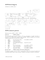
PC Engines ALIX.2 / ALIX.3 / ALIX.6 series system boards 2007-2009 PC Engines GmbH. All rights reserved. PC Engines GmbH www.pcengines.ch tinyBIOS and PC Engines are trademarks of PC Engines GmbH. All other marks and brands are property of their respective owners. ALIX system board 2 5/5/2010 Table of contents Federal Communications Commission Statement 4 CE Declaration of Conformity 4 Compliance information 5 Recycling / disposal 5 Introduction / features 6 OEM options 6 ALIX.2 series 7 ALIX.3 series 8 ALIX.6 series 9 Setup options 10 BIOS upgrade 11 PXE boot 11 Power over Ethernet 11 Hardware compatibility 11 High power radio cards 12 Operating system compatibility 12 FreeBSD 12 FreeDOS, MS-DOS 5.0 12 Linux 12 NetBSD 12 OpenBSD 12 ALIX block diagram 13 ALIX connector pinouts 13 Status LEDs 20 Mode switch 20 Low level programming 20 BIOS POST codes 21 ALIX system board 3 5/5/2010 Federal Communications Commission Statement This device complies with Part 15 of the FCC Rules. Operation is subject to the following two conditions: (1) this device may not cause harmful interference, and (2) this device must accept any interference received, including interference that may cause undesired operation. This equipment has been tested and found to comply with the limits for a Class B digital device, pursuant to Part 15 of the FCC Rules. These limits are designed to provide reasonable protection against harmful interference in a residential installation. This equipment generates, uses and can radiate radio energy. If this equipment is not installed and used in accordance with the manufacturer’s instructions, it may cause harmful interference to radio communications. However, there is no guarantee that interference will not occur in a particular installation. If this equipment does cause harmful interference to radio or television reception, which can be determined by turning the equipment off and on, the user is encouraged to correct the interference by one or more of the following measures: • Reorient or relocate the receiving antenna. • Increase the separation between the equipment and receiver. • Connect the equipment to an outlet on a circuit different from that to which the receiver is connected. • Consult the dealer or an experienced radio/TV technician for help. This board is designed for installation in a shielded enclosure (metal or plastic with conductive coating). Shielded cables are required on LAN and serial ports to assure compliance with FCC regulations. A copy of the test report will be provided on request. CE Declaration of Conformity We, PC Engines GmbH, declare that ALIX.2, ALIX.3 and ALIX.6 series boards, when installed in PC Engines metal enclosures. (case1c1 / case1c2 / box2c), are in conformance with: - EN 61000-6-3 (2005) (emissions, residential and industrial) - EN 61000-6-2 (ESD, susceptibility, residential and industrial) The unit under test is in conformity with the standards mentioned above. A copy of the test report will be provided on request. ALIX system board 4 5/5/2010 Compliance information For FCC, ALIX has been tested as a CPU board, installed in an enclosure, with the top cover removed. No further testing should be required if the board is used with other FCC tested modular components. Please see http://www.fcc.gov/oet/ for more details. The responsible party for FCC is the importer. Testing for CE mark must be done at the level of the complete product, possibly including the wireless cards. Please contact PC Engines for assistance and documentation. For satisfactory resistance to electrostatic discharge events (ESD), the ALIX board should be grounded (e.g. through the mounting holes, or the serial port connector). The USB port on ALIX.2B / ALIX.3B boards is sensitive to ESD events, spurious overcurrent events may be detected in this version. Recycling / disposal Do not discard electronic products in household trash! All waste electronics equipment should be recycled according to local regulations. Information for the recycler: Please cut off Lithium battery, if present, for separate recycling. PC Engines enclosures are made of aluminium. ALIX system board 5 5/5/2010 Introduction / features PC Engines ALIX boards are small form factor system boards optimized for wireless routing and network security applications. • AMD Geode LX CPU, 433 Mhz (LX700) or 500 MHz (LX800) 5x86 CPU, • 256 KB cache (64K data + 64K instruction + 128K L2) • 1 to 3 Ethernet channels (Via VT6105M, 10 / 100 Mbit/s) • 1 or 2 miniPCI sockets for 802.11 wireless cards and other expansion • 1 miniPCI Express socket for GSM / UMTS cards (ALIX.6) • 128 or 256 MB DDR SDRAM, 64 bit wide for high memory bandwidth • 512 KB flash for PC Engines tinyBIOS • CompactFlash + optional 44 pin IDE header for user’s operating system and application • 7 to 18V (absolute maximum) DC supply through DC jack or passive power over Ethernet • 1 serial port (DB9 male, RXD / TXD only) • 2 USB 2.0 ports (optional) • Header for LPC bus (use for flash recovery or I/O expansion) OEM options The following options can be configured for larger orders: • DRAM size (128 MB, 256 MB) • CPU speed (LX700 / LX800 / LX900) • Delete I/O not required by customer • CMOS level serial port (RXD / TXD only) • Optional header for I2C bus • Optional buzzer for “beeps” • Optional RTC battery • ALIX.3: optional AC97 audio codec (headphone + mic) • ALIX.3: optional VGA video • ALIX3: optional pushbutton switch ALIX system board 6 5/5/2010 ALIX.2 series Configuration 2 LAN / 2 miniPCI, or 3 LAN / 1 miniPCI Power supply 7 to 20V DC, about 3 to 4W at Linux idle, peak about 6W without miniPCI cards and USB devices. Suggest a 18V / 15W supply. Center pin = positive, sleeve = ground, 2.1 mm diameter. Temperature range 0 to 50°C. Dimensions 6 x 6” (152.4 x 152.4 mm) ALIX system board 7 5/5/2010 ALIX.3 series Configuration 1 LAN / 2 miniPCI Power supply 7 to 20V DC, about 2.5 to 3.5W at Linux idle, peak about 5W without miniPCI cards and USB devices. Suggest a 18V / 15W supply. Center pin = positive, sleeve = ground, 2.1 mm diameter. Temperature range 0 to 50°C. Dimensions 100 x 160 mm ALIX system board 8 5/5/2010 ALIX.6 series Configuration 2 LAN / 1 miniPCI / 1 miniPCI express (USB only, no PCI Express support) Power supply 7 to 20V DC, about 3 to 4W at Linux idle, peak about 6W without miniPCI cards and USB devices. Suggest a 18V / 15W supply. Center pin = positive, sleeve = ground, 2.1 mm diameter. Temperature range Dimensions 0 to 50°C. 6 x 6” (152.4 x 152.4 mm) ALIX system board 9 5/5/2010 Getting started… - Install a bootable CF card. Hot swap of CF cards is not supported! - Connect serial port to a PC through null modem cable (RXD / TXD crossed over). Set terminal emulator to 38400 8N1, flow control = none or xon-xoff. - Connect Ethernet as needed. - Connect a 18V DC power supply to the DC jack. Power supply should be able to supply at least 12W for some margin. To avoid arcing, please plug in the DC jack first, then plug the adapter into mains. The board should now power on. All three LEDs will light during BIOS POST, then the system will try to boot, and turn off two of the LEDs. ALIX.6B2: one of the LEDs is driven by the miniPCI express card, normally not lit. You should see tinyBIOS startup messages, memory size, CF disk geometry on the serial console. ALIX.3*3 is different, uses Award BIOS. Press Delete to enter setup, Escape to get the boot menu. Setup options To enter setup, type S during the memory test. You should see something like the following: PC Engines ALIX.2 v0.98j 640 KB Base Memory 261120 KB Extended Memory 01F0 Master 848A CF 128MB Phys C/H/S 1002/8/32 Log C/H/S 1002/8/32 BIOS setup: (9) *C* (M) (P) *R* (E) (X) (Q) 9600 baud (2) 19200 baud *3* 38400 baud (5) 57600 baud (1) 115200 baud CHS mode (L) LBA mode (W) HDD wait (V) HDD slave (U) UDMA enable MFGPT workaround late PCI init Serial console enable PXE boot enable Xmodem upload Quit 9 2 3 4 1 sets baud rate to 9600 baud sets baud rate to 19200 baud sets baud rate to 38400 baud sets baud rate to 57600 baud sets baud rate to 115200 baud C L W V U sets CF / HDD to CHS mode sets CF / HDD to LBA mode toggles HDD delay – HDD takes more time to spin up toggles HDD slave – HDD slave detection takes time, normally disabled toggles UDMA enable – use at your own risk M toggles MFGPT workaround – may be required to support high speed timer. See AMD CS5536 data book section 5.16.3 for the gory details. The system may hang during boot if you get it wrong… ALIX system board 10 5/5/2010 P toggles late PCI init – use for FPGA based miniPCI cards that take a long time to come up. Symptom: no interrupt assigned. R toggles serial console enable. Push the switch S1 during startup to get into setup when the serial console is disabled. E toggles PXE boot enable. Defaults to disable as the PXE module has a 60 second time-out. X Xmodem upload – start upload of an executable binary. Intended for flash BIOS update, ask for more information if necessary. Q quit – asks whether to write back the changes to flash (Y) or not (N). Then the system will restart. BIOS upgrade The current BIOS can always be found at www.pcengines.ch/alix2.htm . To upgrade, boot from a CF card to FreeDOS (see www.pcengines.ch/freedos.htm) , then execute the flash upgrader (sb.com). Please do NOT rename the BIOS files, sb.com will automatically pick the correct one for your board. Do not turn off power while the flash upgrade is running, otherwise the flash BIOS may be corrupted. If this happens, the board can be revived using an LPC adapter available from PC Engines. PXE boot PXE boot can be activated either through the E option in setup (always), or by pressing N during memory test (one time). PC Engines cannot provide technical support for the PXE module, too many possible failure points (Intel / Via PXE module, DHCP server, TFTP server, boot image etc). To avoid premature link failure on cold start, please also enable HDD delay in BIOS setup. Power over Ethernet ALIX implements a passive power over Ethernet scheme, using the unused pairs of LAN1 for power. Power can be injected using a passive POE splitter such as PC Engines POE.1A. . ALIX is NOT compatible with 48V / IEEE 802.3af POE. Please use an external splitter if required. When power is fed in through POE, it is possible to “steal” unregulated power through the DC jack. Please note that this port is not fused. The POE input diode is rated for a current of 2A. Hardware compatibility The Commell MP-541D dual port Gigabit Ethernet card uses non-standard PCI ID select assignment. Ask for a modified BIOS if required, use in the primary miniPCI socket only. Alix.2c / alix.3c: High power radio cards require implementation of ECN.027 (see below). ALIX system board 11 5/5/2010 High power radio cards Earlier production boards don’t react kindly to the abuse dished out by high power radio cards. Change the following component values: ALIX.2C R83 = 2.2K ohm (was 1.0K / marking 01B) C98 = 4.7 nF (was no stuff) ALIX.3C R73 = 2.2K ohm (was 1.0K / marking 01B) C93 = 4.7 nF (was no stuff) 2.2K ohm resistors are marked 222 (5%) or 34B. Parts can be supplied to customers on request. Operating system compatibility Please keep in mind that ALIX.2 and ALIX.3 boards do not include a keyboard controller. Some boot loaders may hang and need to be modified. For best performance, include support for AMD Geode LX / CS5536, and use a current driver for the Via VT6105M LAN controller (which supports TCP/IP checksumming and byte aligned transmit buffers, unlike earlier Via Rhine parts). Reboot is best triggered by port 92h. FreeBSD Current versions of FreeBSD may panic due to issues in the EHCI configuration. Disable EHCI driver if problems appear. FreeDOS, MS-DOS 5.0 Tested ok, booting from CF card. Linux Try www.imedialinux.com for a kernel preconfigured with Geode LX drivers. Time drift ? Depending on the system you may need to install the package adj-timex. NetBSD Not yet tested. OpenBSD OpenBSD 4.0-stable and later versions should support AMD Geode LX.GPIO supported by glxpcib(4) driver. Please upgrade to BIOS 0.99 or later to resolve problems with the serial console. ALIX system board 12 5/5/2010 ALIX block diagram Schematics are available online ! ALIX connector pinouts References refer to ALIX.2 / ALIX.3 / ALIX.6. J5/J3/ J5 COM1 serial port The standard PC pinout is used. To connect to a PC, use a null modem or “Laplink” cable. Due to limitations of the AMD CS5536 companion chip, only RXD / TXD are available for your software; handshake signals cannot be observed or controlled ! 1 2 3 4 5 6 7 8 9 DCD RXD# TXD# DTR GND DSR RTS CTS RI J14 / J17 / J19 data carrier detect (input) receive data (input) transmit data (output) data terminal ready (output) ground data set ready (input) ready to send (output) clear to send (input) ring indicator (input) - not available on CS5536 - always driven active - not available on CS5536 - always driven active - not available on CS5536 - not available on CS5536 COM1 serial port (3.3V levels, build option) This header is available on alix.2d / alix.3d / alix.6b and later. This port is connected in parallel with the MAX3243 RS-232 driver, remove this part if CMOS level serial port is desired as an alternative. ALIX system board 13 5/5/2010 1 2 3 4 V3 TXD RXD GND J12 / J4 / J12 3.3V supply transmit data (output) receive data (input) ground COM2 serial port (build option) As an option, the board can be configured with a 4 or 5 pin header with 3.3V CMOS signal levels instead of the normal RS-232 serial port. On alix.2c / alix.3c boards, this port is connected in parallel to COM1, need to remove MAX3243 serial driver to use. Alix.2c / alix.2d -> please add a 1K or 2.2K ohm pull-up resistor to 3.3V on the TXD line. 1 2 3 4 5 V3 TXD RXD GND VCC J3/J1 / J3 3.3V supply transmit data (output) receive data (input) ground 5V supply Ethernet port 1 RJ45 connectors with integrated magnetics are used. This port implements a passive power over Ethernet scheme over the two unused pairs. Do not exceed 20V as the TVS protection diode may start clamping above this voltage. 1 2 3 4 5 6 7 8 TX+ TXRX+ VIN VIN RXGND GND J1, J2 / - / J1 transmit positive transmit negative receive positive power supply (nominal 7 to 20V) “ receive negative power return “ Ethernet ports 2, 3 RJ45 connectors with integrated magnetics are used. These ports do NOT support power over Ethernet. Same pinout as above, but pins 4,5 and 7,8 are not connected. J6/J9 / J6 USB jack Dual USB 2.0 connections. As a build option, 4 pin headers can be installed instead of the USB connector. 1 2 3 4 5 6 7 8 VCC DATA2DATA2+ GND VCC DATA1DATA1+ GND ALIX system board switched +5V supply negative data positive data ground switched +5V supply negative data positive data ground 14 5/5/2010 J19 / - / - USB header (build option) Install to get access to additional USB ports inside the enclosure. 1,2 3 4 5 6 7,8 9 10 VCC DATA4DATA3DATA4+ DATA3+ GND Key GND J4/J2 / J2 +5V supply (not switched / fused) negative data negative data positive data positive data ground key pin ground DC power jack This is a generic DC jack connector with a 2.1mm center pin. Recommended input voltage is +18V. center VIN sleeve GND Positive input voltage Ground J7, J8 / J5, J14 / J8 miniPCI socket These sockets implement the miniPCI interface. Please see schematic for pinout. J9 / - / J9 IDE header (build option) IDE cannot be supported by alix.2*0 / alix.2*1 boards – 5V supply too weak. IDE can be added to alix.2c2 / alix.2c3 / alix.6*2 boards by adding the header, and a 470 ohm resistor in location R50. Please upgrade to the latest BIOS. 1 2 3 4 5 6 7 8 9 10 11 12 13 14 15 16 17 18 19 20 21 22 23 24 25 HDRST# GND HDD7 HDD8 HDD6 HDD9 HDD5 HDD10 HDD4 HDD11 HDD3 HDD12 HDD2 HDD13 HDD1 HDD14 HDD0 HDD15 GND key HDRQ GND HDIOW# GND HDIOR# ALIX system board IDE reset ground IDE data 7 IDE data 8 IDE data 6 IDE data 9 IDE data 5 IDE data 10 IDE data 4 IDE data 11 IDE data 3 IDE data 12 IDE data 2 IDE data 13 IDE data 1 IDE data 14 IDE data 0 IDE data 15 ground key pin (missing) IDE DMA request ground IDE I/O write ground IDE I/O read 15 5/5/2010 26 27 28 29 30 31 32 33 34 35 36 37 38 39 40 41 42 43 44 GND HDIORDY CSEL HDACK# GND HDIRQ nc HDA1 HDPDIA# HDA0 HDA2 HDCS0# HDCS1# HDLED# GND VCC VCC GND GND J10 / J15 / J10 ground IDE I/O ready cable select (pull down) IDE DMA acknowledge ground IDE interrupt no connect IDE address 1 IDE diagnostic, 80 pin cable ID IDE address 0 IDE address 2 IDE chip select 0 IDE chip select 1 IDE led output ground 5V power 5V power ground ground CompactFlash The CompactFlash card is used in True IDE mode. Hot insertion is not supported – please power off the unit before inserting a CF card. 1 2 3 4 5 6 7 8 9 10 11 12 13 14 15 16 17 18 19 20 21 22 23 24 25 26 27 GND D3 D4 D5 D6 D7 CS0# A10 ATASEL# A9 A8 A7 VCC A6 A5 A4 A3 A2 A1 A0 D0 D1 D2 IO16# CD2# CD1# D11 ALIX system board ground IDE data IDE data IDE data IDE data IDE data IDE decode (1F0..1F7) ground ground to select true IDE mode ground ground ground +3.3V power supply ground ground ground ground IDE address IDE address IDE address IDE data IDE data IDE data 16 bit decode, not connected card detect, not connected card detect. not connected IDE data 16 5/5/2010 28 29 30 31 32 33 34 35 36 37 38 39 40 41 42 43 44 45 46 47 48 49 50 D12 D13 D14 D15 CS1# VS1# IOR# IOW# WE# IRQ VCC CSEL# VS2# RESET# IORDY INPACK# REG# DASP# PDIAG# D8 D9 D10 GND IDE data IDE data IDE data IDE data IDE decode (3F6..3F7) not connected IDE read strobe IDE write strobe connected to +3.3V IDE interrupt +3.3V power supply cable select, ground = master not connected IDE reset, active low IDE ready IDE DMA request IDE DMA acknowledge pulled up pulled up IDE data IDE data IDE data ground The CompactFlash specification can be found at www.compactflash.org. J11 / J6 / J11 LPC expansion The LPC port is used in the factory to connect an alternate flash BIOS to start the board when the on-board flash is corrupted or blank. Use PC Engines adapter LPC.1A for this purpose if needed. The LCP port can also be used to connect a super I/O device. Unlike SC1100 based WRAP boards, this port cannot be reprogrammed as GPIO pins. Contact PC Engines for sample schematics if required. 1 2 3 4 5 6 7 8 9 10 11 12 13 14 15 16 17 LCLK0 GND LAD0 GND LAD1 GND LAD2 GND LAD3 GND LFRAME# GND PCIRST# CLK48 ISP VCC GND ALIX system board LPC clock (33 MHz) ground LPC data 0 ground LPC data 1 ground LPC data 2 ground LPC data 3 ground LPC frame ground reset (active low) super I/O clock (48 MHz) high to use LPC flash, low to use on-board flash, pulled low by resistor +5V supply ground 17 5/5/2010 18 19 20 V3 SERIRQ LDRQ# J13 / J8 +3.3V supply serial interrupt LPC DMA request I2C bus (build option) This optional header can be used to connect user specific hardware, e.g. a front panel microcontroller, or for a licensing dongle. See AMD CS5536 data sheet for programming details. 1 2 3 4 +3.3V SMB_SCL SMB_SDA GND power supply I2C clock I2C data ground Starting with alix.2d and alix.6c versions, the following pins have been added: 5 6 7 8 MODESW# RLED1# RLED2# RLED3# same as switch S1 cathode of LED1 cathode of LED2 cathode of LED3 - / J12 / - Headphone out (build option) - / J13 / - Microphone in (build option) Only populated on alix.3*3 version. Starting with alix.3d3, this connector can also be configured to connect to line in. Please see schematics for details, parts marked with – are not populated. - / J11 / - VGA (build option) Only populated on alix.3*3 version. 1 2 3 4 5 6 7 8 9 10 11 12 13 14 15 VGAR VGAG VGAB nc GND GND GND GND USBVCC GND nc DDCDAT HS VS DDCCLK BT1 / BT1 / BT1 VGA red VGA green VGA blue no connect ground ground ground ground +5V supply (fused) ground no connect DDC data horizontal sync vertical sync DDC clock RTC battery (build option) Footprint for CR2032 Lithium battery. Please observe correct polarity, top side of the battery is + positive terminal. For alix.3d and later, also add a jumper on J16 pins 1 to 2. This is the CMOS reset jumper for alix.3d3. ALIX system board 18 5/5/2010 Specification: CR2032, horizontal mount, 20.4 mm lead spacing, for example Renata CR2032FH1 or Panasonic BR2032-1HE. BU1 / BU1 / - Buzzer (build option) Optional audio transducer. The footprint fits a Hycom HY-05 or equivalent. On alix.2c / alix.3d, the driver circuit is not populated, please see page 7 of the schematics for details if you want to add this function. - / - / J18 miniPCI Express The Geode LX CPU, and thus alix.6b2, only supports USB mode, not PCI Express mode. This means that typical GSM / UMTS and WIMAX cards should work, Wifi cards will not. See the schematics for detailed pinout. Please note that LED3# is driven by the miniPCI express card by default. GPIO27 controls the W_DIS# radio inhibit signal instead. Drive low (0) to inhibit, high (1) to enable the miniPCI express radio. Change configuration resistors R140 / R142 / R143 if different behavior is desired. The board has two SIM sockets. J17 is primary, accessed if GPIO1 / ACBEEP is low. J20 on the bottom side is secondary, accessed if GPIO1 is high. Keep in mind that the radio card needs to be reset (e.g. AT+CFUN=1,1) to recognize the new SIM settings. GPIO1 is not initialized properly by the current BIOS, see www.pcengines.ch/file/alixllc.zip / gpio1.8 for sample code to control this pin. ALIX system board 19 5/5/2010 Status LEDs Status LEDs are all turned on by the BIOS on power up. The BIOS will turn off LEDs 2 and 3 before booting the operating system. Location GPIO read port write port LED1 (left) G6 port 06100h bit 6 port 06100h bit 6 / 22 LED2 (middle) G25 port 06180h bit 9 port 06180h bit 9 / 25 LED3 (right) G27 port 06180h bit 11 port 06180h bit 11 / 27 The CS5536 GPIO ports are programmed by 32 bit atomic writes. This avoids the need for read / modify / write operations and the locking issues they entail. For example, to turn off LED1 (high), write 0000’0040h to port 06100h. To turn on LED1 (low), write 0040’0000h. Multiple port bits can be changed at the same time. On ALIX.6, please note that LED3# is driven by the miniPCI express card by default. GPIO27 controls the W_DIS# radio inhibit signal instead. Drive low (0) to inhibit, high (1) to enable the miniPCI express radio. Mode switch The mode switch can be accessed by software as follows: Location GPIO read port MODESW# G24 port 061b0h bit 8 (active low, 0 = switch pressed) Low level programming Please see www.pcengines.ch/file/alixllc.zip for sample code. ALIX system board 20 5/5/2010 BIOS POST codes tinyBIOS writes POST / diagnostic codes to port 80h. To make these codes visible, use a miniPCI POST card such as PC Engines POST.5A. POST codes are: 01 02 03 04 05 06 07 08 09 0a 0b 0c 0d 0e 0f 10 11 12 13 14 15 16 17 18 19 1a 1b 1c 1d 1e 1f 20 21 22 23 24 25 26 27 00 reset entry chipset initialization detect base memory size initialize shadow RAM init mono video disable PCI devices test low 64KB of DRAM initialize stack BIOS checksum super I/O initialization RTC test refresh / 8254 test speed-dependent chipset regs test 8237 DMA test DMA page registers test 8254 registers test keyboard controller init timer, DMA, 8259... test 8259 mask registers test low 640KB init vectors PCI plug & play shadow video BIOS look for VGA BIOS sign-on prompt second keyboard test extended memory test enable interrupts test / init RTC init floppy disk option ROM scan test parallel ports test serial ports enable coprocessor floppy init hard disk init PS/2 mouse detect timer/RTC check OEM boot decision point boot 33 F7 NMI low 64KB memory test failed ALIX system board 21 5/5/2010