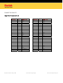
1
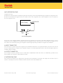
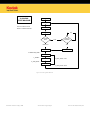
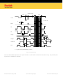
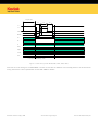
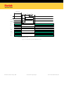
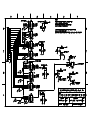
USERS MANUAL
Revision 8.0 MTD/PS-0215
January 2, 2008
KODAK KAF SERIES CCD DIGITAL REFERENCE
EVALUATION BOARD USERS MANUAL
TABLE OF CONTENTS
Introduction................................................................................................................................................................................. 5
Overview ...................................................................................................................................................................................... 5
Specifications .............................................................................................................................................................................. 6
Outputs: .......................................................................................................................................................................................6
Inputs: TTL.................................................................................................................................................................................6
Architecture Overview ................................................................................................................................................................. 7
Master Clock ...............................................................................................................................................................................7
PLD1 ............................................................................................................................................................................................7
PLD2 ............................................................................................................................................................................................7
CCD Clock Drivers.......................................................................................................................................................................7
CCD Bias Voltages.......................................................................................................................................................................8
CCD Image Sensor ......................................................................................................................................................................8
A/D Converter: Analog Devices AD9816 .....................................................................................................................................8
Emitter Follower .........................................................................................................................................................................8
AC Coupling Capacitor ................................................................................................................................................................8
Power on Clear / Reset ...............................................................................................................................................................8
JTAG Header................................................................................................................................................................................8
Unit Integration Time ..................................................................................................................................................................9
J6 Input Connector ......................................................................................................................................................................9
J4 Output Connector ...................................................................................................................................................................9
J7 Integration Sync......................................................................................................................................................................9
J1, J2 Imager Board Connectors..............................................................................................................................................10
Power Supplies..........................................................................................................................................................................10
J5 Power Connector..................................................................................................................................................................10
Board Requirements:................................................................................................................................................................ 11
Power Supply.............................................................................................................................................................................11
Inputs .........................................................................................................................................................................................11
Outputs ......................................................................................................................................................................................11
JTAG Programming...................................................................................................................................................................11
Configuration Modes................................................................................................................................................................. 12
Line/Switches Modes ................................................................................................................................................................12
Still/Free-Run Modes................................................................................................................................................................12
AD_IN/EX Modes .......................................................................................................................................................................13
EXT: ........................................................................................................................................................................................13
INT:.........................................................................................................................................................................................13
Adjustments...............................................................................................................................................................................14
CCD Modes ................................................................................................................................................................................14
Binning Modes...........................................................................................................................................................................14
Integration Modes .....................................................................................................................................................................14
Frame Grabber Diagnostic Modes ...........................................................................................................................................14
Power Supply Modes.................................................................................................................................................................15
Switching Power Supply ........................................................................................................................................................15
External Supply Operation ....................................................................................................................................................15
Functionality ..........................................................................................................................................................................15
CCD Imager Boards .................................................................................................................................................................. 16
Adjustments...............................................................................................................................................................................16
Fixed Bias Voltages: ..............................................................................................................................................................16
Variable Bias Voltages:..........................................................................................................................................................16
©Eastman Kodak Company, 2008
www.kodak.com/go/imagers
Revision 8.0 MTD/PS-0215 p2
Output Selection for Sensors with Two Outputs ......................................................................................................................17
Timing........................................................................................................................................................................................ 18
Fixed Timing: .............................................................................................................................................................................18
Variable Timing: ........................................................................................................................................................................18
Other Parameters ..................................................................................................................................................................... 18
Fixed Parameters:.....................................................................................................................................................................18
Variable Parameters: ................................................................................................................................................................18
Figures, Tables, Timing Diagrams, and Performance Data..................................................................................................... 19
System Noise Floor Vs. Operating Frequency .........................................................................................................................35
Connector Pinouts.....................................................................................................................................................................37
Imager Board Connectors J1, J2 ..........................................................................................................................................37
Input Connector J6 ................................................................................................................................................................38
Output Connector J4..............................................................................................................................................................39
Integrate Sync Connector J7.................................................................................................................................................40
Power Connector J5 ..............................................................................................................................................................40
JTAG Connector J8 ................................................................................................................................................................40
References ................................................................................................................................................................................ 41
Ordering Information ................................................................................................................................................................ 41
Warning: Life Support Applications Policy............................................................................................................................... 41
Revision Changes...................................................................................................................................................................... 41
Appendix.................................................................................................................................................................................... 42
Appendix1:
Part Number Availability ................................................................................................................................42
Appendix 2:
Parts List.........................................................................................................................................................43
Appendix 3:
Imager Board Schematics..............................................................................................................................46
©Eastman Kodak Company, 2008
www.kodak.com/go/imagers
Revision 8.0 MTD/PS-0215 p3
TABLE OF TABLES
Table 1: Board Inputs, Outputs, Switches....................................................................................................................................22
Table 2: CCD Modes......................................................................................................................................................................23
Table 3: Binning Modes ................................................................................................................................................................23
Table 4: Binning Modes when Configured for use with the KAF-16801E/LE ............................................................................24
Table 5: KAF-4301E SW2 Pixel Rate Settings ..............................................................................................................................24
Table 6: Integration Time Modes..................................................................................................................................................25
TABLE OF FIGURES
Figure 1: System Block Diagram .................................................................................................................................................19
Figure 2: Clocking State Machine ................................................................................................................................................20
Figure 3: AD9816 Register Configuration ....................................................................................................................................21
Figure 4: Pixel Rate Timing ..........................................................................................................................................................26
Figure 5: Line Rate Timing for KAF-0261E, 0402E, 1001E, 1301E, 1402E, .................................................................................27
Figure 6: Line Rate Timing for KAF-16801E/LE Sensors ............................................................................................................28
Figure 7: Frame rate timing for the KAF-0261E, 0402E, 1001E, 1301E, 1402E,.........................................................................29
Figure 8: Frame Timing for the KAF-3200ME Sensor.................................................................................................................30
Figure 9: Pixel Rate Timing for the KAF-3200ME, KAF-16801E, KAF-16801LE Sensors ..........................................................31
Figure 10: Still Mode: Flush and Integration Timing...................................................................................................................32
Figure 11: Free Run Mode: Integration Timing............................................................................................................................32
Figure 12: Binning Mode Timing (2x2 binning shown).................................................................................................................33
Figure 13: Measured Linearity .....................................................................................................................................................34
Figure 14: Measured Performance: Noise Floor.........................................................................................................................34
Figure 15: Measured Performance: Dynamic Range ..................................................................................................................35
Figure 16: Measured Performance: A/D Programmable Gain ...................................................................................................36
©Eastman Kodak Company, 2008
www.kodak.com/go/imagers
Revision 8.0 MTD/PS-0215 p4
INTRODUCTION
The Kodak Digital Science TM KAF Series CCD Digital Reference Evaluation Board provides a powerful platform to quickly
and easily implement a Kodak Digital Science Full Frame or Blue Plus Full Frame CCD image sensor in a prototype
imaging system.
The Evaluation Board also serves as a useful reference design that will save considerable time and cost in the
development of a product prototype. The programmable logic architecture, bias supplies, clock drivers and analog signal
processing chain can be readily used, with application specific modifications, in a camera production design.
The Evaluation Board is designed to be flexible, and has the ability to operate many different Kodak Full Frame image
sensors at different operating frequencies. Consult Image Sensor Solutions (ISS) to obtain information for optimizing the
reference design to operate a specific image sensor at a specific operating frequency.
OVERVIEW
The KAF Series Digital Reference Evaluation Board serves as a complete, self-contained, CCD image acquisition subsystem. The user simply applies power, and an IMAGE_AQUIRE TTL pulse to begin capturing digital images. Differential
TTL frame grabber sync pulses (Frame, Pixel and Line rate) are provided to facilitate easy connection to a frame grabber.
In the still capture mode, application of the IMAGE_ACQUIRE signal results in flushing of the CCD, then integration, then
clocking out of a full frame of image data. In free-run mode, an acquisition signal is not needed; the board is free running
and continuous frames of 12 bit information stream out.
12 Bit Output
Image_Acquire
©Eastman Kodak Company, 2008
CCD Reference
Evaluation Board
www.kodak.com/go/imagers
Revision 8.0 MTD/PS-0215 p5
SPECIFICATIONS
Maximum Data Rate
6MHz
Resolution
12 Bits
Frame Rate
Depends on Data Rate, CCD Array size, and Integration time.
OUTPUTS:
D[11..0]
Differential TTL
Frame Grabber Syncs
Differential TTL
Integration Sync
TTL
INPUTS: TTL
Serial Clock
10 MHz Maximum
PGA Gain Range
1X to 6X
PGA Gain Resolution
256 steps
Offset Range
-100mV to +100mV
Offset Resolution
256 steps
Temperature Range Board
0 - 70°C
Temperature Range CCD
-50 to +70°C typical
Power Supplies
Typical Current
Switching Power Supply
Supply
+5V
+18V
-18V
Minimum
+4.9V
+17V
-20V
Nominal
+5V
+18V
-18V
Maximum
+5.1V
+20V
-13V
Disabled
1000mA
120mA
100mA
Enabled
1500mA
-
Electrons per A/D count
29.2 @ 5MHz, 2.5X Gain setting (Assuming on-chip CCD amplifier gain CCD of
10µV/electron)
RMS Dark Noise
1.9 LSB typical @ 5MHz, 2.5X Gain setting
System Noise Floor
56 electrons @ 5MHz, 2.5X Gain setting (Assuming on-chip CCD amplifier gain of
10µV/electron)
©Eastman Kodak Company, 2008
www.kodak.com/go/imagers
Revision 8.0 MTD/PS-0215 p6
ARCHITECTURE OVERVIEW
A complete Block Diagram of the CCD Digital Reference Evaluation Board is shown in .
MASTER CLOCK
The Master Clock runs at eight times the Pixel clock frequency. The maximum pixel clock frequency is 6 MHz, which yields
a maximum system clock frequency of 48 MHz. For slower Pixel clock frequencies, decrease the master clock frequency.
The Default setting of the evaluation board is a 40 MHz system clock, with a pixel clock frequency of 5 MHz.
The KAF-4301E is an exception to this. It provides pixel frequencies of 2.5MHz and 1.25 MHz by dividing the 40MHz master
clock by 16 and 32. The pixel frequency is selected using SW2. This is an 8-position switch that usually selects a CCD
binning mode (see section Binning Modes). The KAF-4301E timing program does not support binning at this time and,
instead, uses this switch to select the pixel rate (see Table 5: KAF-4301E SW2 Pixel Rate Settings). The pixel rate is 1.25
MHz when SW2 is set to position 0 and 2.5 MHz when set in any other position.
PLD1
PLD1 contains the Clocking State Machine that controls the operational flow of the evaluation board (Figure 2: Clocking
State Machine). PLD1 generates the CCD clock timing, A/D converter timing and frame grabber sync signals. The PLD1
controls the image line and frame length [dependent upon the CCD switch settings], as well as the horizontal and vertical
CCD clock timing [dependent upon the binning mode BIN switch settings.]
PLD2
PLD2 controls the integration timing, which is dependent upon the INT switch settings. PLD2 also programs the AD9816’s
registers to a default condition upon power up via a three wire serial interface. Additionally, if the user chooses to adjust
the AD9816’s register settings, the PLD2 controls the programming of these registers.
CCD CLOCK DRIVERS
Elantec clock drivers, designed to drive the large capacitance loads presented by the clock gates of the CCD, are used to
generate the horizontal and vertical clocks. The Elantec drivers accept TTL inputs, and level shift to the required peak-topeak voltage swing of the CCD clocks. The peak-to-peak swing of the clocks is adjustable. The outputs of the drivers are
AC coupled, providing adjustable offset of the clocks from the negative rail to the positive rail. Using a separate IC for each
vertical clock (V1,V2), a maximum 4 amp output drive current per vertical clock channel is available. A single IC is used to
drive H1, and H2, giving a maximum 2A output drive current per Horizontal clock channel.
The reset clock driver utilizes two fast switching transistors, designed for a fast switching input signal with a narrow pulse
width. The peak-to-peak voltage swing and the offset voltage are adjustable.
©Eastman Kodak Company, 2008
www.kodak.com/go/imagers
Revision 8.0 MTD/PS-0215 p7
CCD BIAS VOLTAGES
CCD bias voltages (VRD, VOG, VLG) are supplied by filtered outputs of adjustable potentiometers. Fixed CCD bias voltages
(LOD, VSS, GUARD) are supplied by filtered outputs of voltage dividers.
CCD IMAGE SENSOR
This evaluation board supports the following Kodak Full Frame (KAF) CCD image sensors:
KAF-0261E, KAF-0402E, KAF-0402ME, KAF-0401LE, KAF-1001E, KAF-1301E, KAF-1301LE, KAF-1402E, KAF-1402ME, KAF1602E, KAF-1602LE, KAF-3200E, KAF-3200ME, KAF-4202, KAF-6303E, KAF-6302LE, KAF-16801E, KAF-16801LE, KAF4301E
A/D CONVERTER: ANALOG DEVICES AD9816
The AD9816 is a 12 bit, 6 MSPS CCD analog signal processor. The IC provides an integrated correlated double sampling
(CDS), 8 bit programmable gain, and 8 bit DC offset adjust. Timing signals are provided by PLD1. Default register values
are downloaded from PLD2 upon power up. Alternate programming of its registers can be achieved via external serial
interface or by manually setting the address and data switches on the board and pressing the capture button.
EMITTER FOLLOWER
The video out of the CCD is buffered using a bipolar junction transistor in the emitter follower configuration.
AC COUPLING CAPACITOR
A 1200pF input coupling capacitor removes the DC component of the video signal.
POWER ON CLEAR / RESET
Resets and initializes the board on power up or when the Reset button in pressed.
JTAG HEADER
A 10-pin header provides the user with the ability to reprogram the Altera 7000S PLDs in system via Altera’s ByteBlaster
programming hardware.
©Eastman Kodak Company, 2008
www.kodak.com/go/imagers
Revision 8.0 MTD/PS-0215 p8
UNIT INTEGRATION TIME
Integration Timing:
The amount of time the CCD is exposed to light before clocking out the accumulated charge is called the integration time.
An RC circuit and Schmitt trigger inverter are used to set the unit integration time. Total integration time is a multiple of
the unit integration time.
Altera Timing
Rpot
INTEGRATE
C1
Set Unit Integration
The circuit is set to toggle at 100 Hz, providing a fixed unit integration time of 10ms. The actual integration time is set to a
multiple of the unit integration time using an internal integration counter in PLD2. The user can choose an integration time
from 10ms to 10 seconds by setting the integration switches appropriately (see Table 6: Integration Time Modes)
J6 INPUT CONNECTOR
This connector is used to input control signals to the evaluation board. This is an optional feature; all control lines can be
set via on-board switches. Images can be acquired using the on-board image capture button. No external digital inputs are
needed to acquire images.
J4 OUTPUT CONNECTOR
The J4 output connector provides 12 bits of video data in RS422 differential TTL format. J4, additionally, provides three
frame grabber sync signals in differential TTL format.
J7 INTEGRATION SYNC
This connector provides a sync signal that is high during the integration time period. The signal can be used to sync a
shutter or LED light source to the evaluation board, and can source up to 80mA at 5V.
©Eastman Kodak Company, 2008
www.kodak.com/go/imagers
Revision 8.0 MTD/PS-0215 p9
J1, J2 IMAGER BOARD CONNECTORS
CCD Daughter Boards plug into these connectors. The daughter boards route the clock and bias traces from the timing
board to the proper pins of the CCD.
POWER SUPPLIES
An onboard switching supply provides all of the voltages necessary to operate the CCD Digital Reference Evaluation Board,
from a single +5V source.
Switching supplies can, however, be a source of low-level asynchronous noise. If asynchronous noise is present and
objectionable in an application, the internal switching supply can be disabled and external low-noise linear supplies can be
used to power the board. The procedure for configuring the board to accept external supplies is detailed Under Power
Supply Modes
J5 POWER CONNECTOR
The power connector is a 5-pin connector with +5V, +18V, -18V and two AGND connections. If the switching power supply
is used to generate the +15 and -10V supplies, then only an external +5V supply needs to be brought in through J5.
Otherwise, all three power supplies must be connected to the board via J5.
©Eastman Kodak Company, 2008
www.kodak.com/go/imagers
Revision 8.0 MTD/PS-0215 p10
BOARD REQUIREMENTS:
POWER SUPPLY
The board requires only a single +5V, 1.5 Amp or greater power supply to operate. An on board switching power supply
generates the necessary +15V, 120mA and –10V, 120mA power supplies from the 5V input. Although extensive filtering is
done on board, the power supplied to the board must be quiet and stable in order to achieve the best possible
performance.
(See Power Supply Modes, for an alternative way to power the board.)
INPUTS
In the Free-Run mode, the evaluation board requires no input signals to begin acquiring images.
In Still mode, the evaluation board will acquire a single image on the falling edge of the Image_Acquire control line. This
can be accomplished via the push button (S4) or, remotely, by utilizing the Image_Acquire control line.
See Section Still/Free-Run Modes for more information on Still and Free-Run modes.
See Sections Line/Switches Modes and section AD_IN/EX Modes for information on additional optional inputs.
OUTPUTS
D[11..0] (+/-)
12 bits of Differential TTL Digital information
INTEGRATE
A signal provided to allow the user to synchronize the strobing of LED illuminators or opening of a
shutter, during the integration period.
FRAME (+/-)*
Differential TTL Frame grabber vertical sync signal.
LINE (+/-)*
Differential TTL Frame grabber horizontal sync signal.
PIX (+/-)*
Differential TTL Frame grabber pixel sync
Note: These sync signals can be modified if necessary to accommodate different Frame Grabbers.
JTAG PROGRAMMING
Altera 7000S In System Programmable (ISP) PLD’s are used on this board. A ten-pin header (J8) is provided to allow for
the programming of these PLD’s. Since these parts are re-programmable, custom digital logic can be implemented for
timing and mode adjustments or additions. Any custom implementation can be made quickly and easily to via the JTAG
programming interface provided by this connector.
©Eastman Kodak Company, 2008
www.kodak.com/go/imagers
Revision 8.0 MTD/PS-0215 p11
CONFIGURATION MODES
The following modes of operation are available to the user:
LINE/SWITCHES MODES
The Line/Switches Jumper (SW5) Selects whether some of the board settings will be controlled externally through the J6
connector (Line), or via the on-board switches (Switches). If this switch is set to Line, then the integration time and the
binning mode must be set remotely via digital I/O. The still/free-run mode switch (SW3, 3-position switch) can also be set
externally when the Line mode is selected. Set SW3 to the middle position if it is desired to control this line externally.
STILL/FREE-RUN MODES
The “Still/Free-Run” switch (SW3) is a three-position switch that selects whether the board will operate in the still mode,
or a free-running mode.
If SW3 is placed in the middle position (“LINE”), the image capture mode is determined by the voltage on the STILL/FREERUN pin on the input connector (J6-27). Setting this line LOW selects the free-run mode, and setting it HIGH selects the
still mode.
In still mode, the Image_Acquire control line must be strobed in order to acquire a single image. This is accomplished by
either pressing the on-board acquire button (S4) or, remotely, by bringing the Image_Acquire line low and then back high.
The detection of the falling edge of this signal starts the image acquisition process.
The still mode acquisition process is as follows:
1.
The CCD is flushed of all accumulated charge.
2.
The CCD is exposed to light during the integration time.
3.
The image is clocked out of the CCD. The system then waits for the next Image_Acquire signal.
In the Free-Run mode, the system will continuously capture images and clock them out. No flushing is done, as the
clocking out of the previous image serves this same purpose.
See Figure 2: Clocking State Machine for the Clocking State Machine Diagram.
©Eastman Kodak Company, 2008
www.kodak.com/go/imagers
Revision 8.0 MTD/PS-0215 p12
AD_IN/EX MODES
The board comes with an Analog Devices AD9816 12 bit A/D converter on board. This A/D has several features, such as
multiple configurations, programmable gain, and offset registers which require initialization and/or programming on
power up. The programming of these registers is done via a three wire serial interface.
EXT:
A three wire serial interface is provided on the J6 connector of the board, and the AD9816 registers can be controlled
remotely via these when the A/D_IN/EX Jumper (SW4) is set to EXT. See Figure 3: AD9816 Register Configuration for
AD9816 serial timing diagrams and information.
INT:
If it is not desired to control the programming of the A/D’s registers remotely, set Jumper SW4 to INT. PLD2 contains a
state machine that serially loads in the following default values to these registers upon power up.
A/D Default Register Settings:
No. of channels:
1
Mode:
CDS Mode
Input Span:
3V
Channel Selected:
Green
Red PGA Gain*:
1
Green PGA Gain:
1
Blue PGA Gain*:
1
Red Offset*:
0mv
Green Offset:
0mv
Blue Offset*:
0mv
Note: Although the Red and Blue channels are not used, these registers are still initialized to these default settings
©Eastman Kodak Company, 2008
www.kodak.com/go/imagers
Revision 8.0 MTD/PS-0215 p13
ADJUSTMENTS
Adjustments can be made to the A/D registers during operation of the board by utilizing the DATA dipswitch (SW10), the
ADDRESS switch (SW9), and the Image_Acquire control line. After setting SW9 to the desired Address, and SW10 to the
desired Data, send an Image_Acquire signal either by pressing the Image_Acquire button or remotely via the J6 connector
control line. This will load the new value into PLD2 and a state machine inside the PLD will then serial load the new data
into the A/D’s register. This is true whether or not the board is running in Still or Free Run Mode. (See Figure 3: AD9816
Register Configuration for more information on the AD9816 registers.)
CCD MODES
The CCD Select switch (SW1) setting determines the line and frame length timing.
This switch is pre-set at the ISS. (See Table 2: CCD Modes)
BINNING MODES
The BIN Select switch (SW2) setting determines the Binning mode operation. (Table 3: Binning Modes)
INTEGRATION MODES
The INT Select switches (SW6, SW7) settings determine the Integration Time.
SW6 is the Coarse Adjust. SW7 is the Fine Adjust. (Table 6: Integration Time Modes)
FRAME GRABBER DIAGNOSTIC MODES
When set to ENABLE, the Sync_Test_Enable switch (SW12) tri-states the 12-bit output bus out of the A/D converter, and
enables the output of either the pixel number or the line number onto the output bus, depending on how the
Sync_Test_pix/line Jumper is set (SW11). This provides a diagnostic test to make certain the Frame Grabber is
synchronized correctly with the board.
The line counter in PLD1 is a binary up-counter, therefore the line count that is output to the output bus will increment
sequentially (0,1,2,3,4,5.....) until the last line in the frame.
The pixel counter in PLD1 is a gray code up counter, therefore the pixel count that is output to the output bus will
increment in gray code transition counts (0,1,3,2,6,7,5,4......) until the last pixel in the line.
©Eastman Kodak Company, 2008
www.kodak.com/go/imagers
Revision 8.0 MTD/PS-0215 p14
POWER SUPPLY MODES
Power can be supplied to the board in one of two ways:
Switching Power Supply
The board comes supplied with a 500 kHz switching power supply (Linear Technologies LT1372). If it is desired to utilize the
on-board switching supply, the board should be configured as follows:
1.
Connect a 5V, 1.5A or greater lab supply to the J5 power connector.
2.
Install Jumper 6 and Jumper 4.
3.
Remove Jumper 7 and Jumper 5.
4.
Set Jumper 1 to the ON position.
External Supply Operation
To disable the on-board switching supply and operate using external supplies:
1.
Remove Jumpers 4 and 6;
2.
Install Jumpers 5 and 7;
3.
Move Jumper 1 to the “OFF” position to disable the switching power supply;
4.
Connect +18V, -18V, and +5V to power input connector J5.
Functionality
The switching supply generates +15V and –10V supply “islands”. The same is true for the +15V and –10 V regulators on the
board. Jumpers 4 and 6 connect the switcher supplies to the +15V, -10V power plane. Jumpers 5 and 7 connect the
regulated outputs to the +15V, -10V power plane. Jumper 1 either enables or disables the LT1372 Switcher.
©Eastman Kodak Company, 2008
www.kodak.com/go/imagers
Revision 8.0 MTD/PS-0215 p15
CCD IMAGER BOARDS
Each CCD has an imager board. The imager boards route the bias voltage traces from the timing board through
connectors J1 and J2 to the appropriate pins on the device. The imager boards contain the Horizontal and Reset clock
driver ICs as well as the emitter-follower circuit that buffers and drives the video signal down to the timing board.
ADJUSTMENTS
Fixed Bias Voltages:
Fixed Voltages:
VDD
+15V
LOD/GUARD
+10V
VSUB
0V
VSS
0 to +2.1V*
Note: The VSS bias voltage is set by the inclusion of up to three series diodes on the imager board. Therefore 0V is
achieved by shorting across all three diode positions. This bias is preset at the factory depending on the appropriate CCD
specification.
Variable Bias Voltages:
Variable Voltage:*
VOG
VRD
VLG
V_PP
VCLK
H_PP
HCLK
R_PP
RCLK
Function
Adjustment Potentiometer
(vertical clk peak to peak swing )
(vertical clk level adjust)
(horizontal clk peak to peak swing )
(horizontal clk level adjust)
(reset clk peak to peak swing)
(reset clk level adjust)
R12
R11
R13
R17
R67
R64 (imager board)
R14 (imager board)
R18 (imager board)
R27 (imager board)
Note: These voltages are optimized for the particular KAF Series image sensor being used and are fixed at the factory
according to the image sensor specification. Adjustments should not be made to them without consulting the ISS.
©Eastman Kodak Company, 2008
www.kodak.com/go/imagers
Revision 8.0 MTD/PS-0215 p16
OUTPUT SELECTION FOR SENSORS WITH TWO OUTPUTS
The KAF-1001E, KAF-0261E, and KAF-4301E sensors have two video outputs. The outputs have different gain and one of
them is selected depending on the application. The imager daughter boards for these sensors have two jumpers that must
be set correctly to enable the desired output.
To select the high gain output, Vout2:
Set J3 to the VID2 position:
1
VID
2
J3
Set the two jumpers on J4 as follows:
J4
Bias
H21
H2
H22
Bias
To select the low gain output, Vout1:
Set J3 to the VID1 position:
1
VID
2
J3
Set the two jumpers on J4 as follows:
J4
Bias
H21
H2
H22
Bias
Note: The schematic for the KAF-1001 imager daughter board contains an error. The library element for the imager
indicates that pin 5 is Vout1 and pin 12 is Vout2. These are incorrect and are reversed in that part of the schematic.
However, the labeling on the imager board is correct. Only the pin labeling on the schematic is incorrect.
©Eastman Kodak Company, 2008
www.kodak.com/go/imagers
Revision 8.0 MTD/PS-0215 p17
TIMING
FIXED TIMING:
H1, H2
VARIABLE TIMING:
V1, V2 (binning modes)
RESET (binning modes)
CLAMP (binning modes)
SAMPLE (binning modes)
A/D Clock (binning modes)
See Timing Diagram 1 – Figure 4: Pixel Rate Timing
See Timing Diagram 3 -Figure 12: Binning Mode Timing (2x2 binning shown)
Note: Not available with the KAF-16801E, KAF-16801LE and KAF-4301E image sensors.
OTHER PARAMETERS
FIXED PARAMETERS:
Flush Duration: (4000 lines)
VARIABLE PARAMETERS:
Pixel frequency: The pixel frequency is 1/8 the master clock. The maximum pixel frequency is 6MHz. To run the board at a
slower pixel rate, decrease the system clock frequency, keeping in mind the 1/8 relationship. (e.g. for a 4 MHz pixel rate,
use a 32 MHz system clock)
Line length
(Depends on CCD mode)
Frame length
(Depends on CCD mode)
Vwidth (Depends on pixel frequency, 64 pixel counts wide)
Unit Integration:The integration clock frequency is set by a RC circuit of R6 and C6 and is adjusted to 100Hz at the factory,
creating a unit integration time of 10ms. By adjusting R6, the unit integration time can be varied. Because all of the
integration time settings in Table 6: Integration Time Modes are multiples of this unit integration time, the values would
need to be recalculated for any new unit integration time.
©Eastman Kodak Company, 2008
www.kodak.com/go/imagers
Revision 8.0 MTD/PS-0215 p18
FIGURES, TABLES, TIMING DIAGRAMS, AND PERFORMANCE DATA
J5
+5V
7414
C
10uF
-18V
J8
R
1K
-10V
+18V
Unit Integration Time
+5V
+15V
LT1372
Switching
Supply
10 pin JTAG
Header
Power_on_clear
J6
34 pos
VDD
VRD
J1 24 position connector
Vclks Driver
CCD Daughter Board
Altera
7000S
PLD 2
Capture Button
Hclks Driver
CCD
Sensor
Rclk Driver
8 bit
Line
Drivers
Still/FreeRun
Int[5..0]
Bin[2..0]
VCC
Emitter
Follower
Altera
7000S
PLD 1
J2 24 position connector
Guard
8 bit
Line
Drivers
VOG
40 Mhz
Clock
VSS, VLG
VSUB
1200 pF
VCC
SW1
J4 (40 pos Connecter)
Switch_CCD[3..0]
CDSCLK1
CDSCLK2
SW2
ADCCLK
Switch_Bin[2..0]
Video in
AD9816
12 Bits
Line/Switches
VCC
SW3
Pixclk
Frame
Line
SCLK
SDATA
SLOAD
Switch_Int[5..0]
SW4
2X
Octal
Latch
4X
Diff
TTL
Line
Drivers
J7
A/D_in/ex
(LED/Shutter Sync)
Figure 1: System Block Diagram
©Eastman Kodak Company, 2008
www.kodak.com/go/imagers
Revision 8.0 MTD/PS-0215 p19
CLOCKING
STATE MACHINE
Power ON
CLEAR_ALL
CLOCK = EIGHTH CLOCK
SET-UP
RESET = POWER ON CLEAR
INITIALIZE
STILL/FREERUN?
NO
STILL
IMAGE
ACQUIRE?
FREE-RUN
YES
INTEGRATION
FLUSH
INTEGRATION_DONE
V_TRANSFER
V_ENABLE
H_TRANSFER
V_XFER_DONE = LOW
H_XFER_DONE
LINE_CHECK
V_XFER_DONE = HIGH
Figure 2: Clocking State Machine
©Eastman Kodak Company, 2008
www.kodak.com/go/imagers
Revision 8.0 MTD/PS-0215 p20
Address
Register
Function
0
Configuration Register
bit 7 MSB
bit 6
bit 5
Default
Programming
1
2
3
4
5
6
7
bit 4
bit 3
bit 2
bit 1
bit 0
MUX Register
bit 7
bit 6
bit 5
bit 4
bit 3
bit 2
bit 1
bit 0
Red PGA Register
Green PGA Register
Blue PGA Register
Red Offset Register
Green Offset Register
Blue Offset Register
test mode bit
test mode bit
CDS mode bit
input span
input span
channel mode
channel mode
test mode bit
test mode bit
channel sequence
channel sequence
channel select
channel select
channel select
test mode bit
test mode bit
always 0
always 0
High for CDS
Low for SHA mode
High for 3V
High for 1.5V
High for 3 channel
High for I channel
Always 0
0
0
1
always 0
High for BGR
High for RGB
High for Red
High for Green
High for Blue
always 0
always 1
1X to 6X*
1X to 6X*
1X to 6X*
-100mv to 100mv**
-100mv to 100mv**
-100mv to 100mv**
0
0
0
0
1
0
0
1
0 (1X)
0 (1X)
0 (1X)
0 (0mV)
0 (0mV)
0 (0mV)
1
0
0
1
0
Note: PGA Gain = 1+(gain code/ 51.2) ** 01111111 = +100mV, 00000000 = 0 mV, 11111111 = -100mV
R/W* A2
A0
D7
D0
SLOAD
SDATA
SCLK
3 Wire Serial Interface Timing
* R/W Low for Write, High for Read
Figure 3: AD9816 Register Configuration
©Eastman Kodak Company, 2008
www.kodak.com/go/imagers
Revision 8.0 MTD/PS-0215 p21
Switches
Inputs
Line/Switches
Select where control of modes comes from
Switch_Int[5..0]
Switch_Bin[2..0]
Switch_CCD[3..0]
Still/Free-Run
A/D_in/ex
Sync_test_pix/line
Sync_test_enable
Integration timing control lines
Binning mode control lines
Device Select (KAF 0400, KAF1600 ... )
Selects mode of operation
Select how A/D programming is controlled
Select frame grabber diagnostic to be performed
Enable/Disable frame grabber sync test
System_clk
8X Pixel clock (48 MHz maximum)
integrate_clk
Image_Acquire
Unit Integration Time clock
Still mode image acquisition command line, OR,
Capture button input
Integration timing control lines
Binning mode control lines
For A/D use
For A/D use
For A/D use
10-pin header for ISP
Int[5..0]
Bin[2..0]
Serial Clock
Serial Data
Serial Load
JTAG Header
Outputs
Dout[11..0](+/-)
12 Bits Differential TTL Digital information
FRAME (+/-)
LINE (+/-)
PIX (+/-)
INTEGRATE
Differential TTL frame grabber frame sync signal
Differential TTL frame grabber line sync signal
Differential TTL frame grabber pixel sync signal
Active high signal indicates when in integration state. Can be used to
sync LED’s or shutter with this state.
Table 1: Board Inputs, Outputs, Switches
©Eastman Kodak Company, 2008
www.kodak.com/go/imagers
Revision 8.0 MTD/PS-0215 p22
CCD Switch Setting
CCD
Pixels/Line
Lines/Frame
0*
1
2
3
4
5
6
7
8
9
A
B
C
Test Mode1 or KAF-16801E/LE
KAF-1401E
Test Mode 2
KAF-1301E, KAF-1301LE
KAF-4202
KAF-1602E, KAF-1602LE
KAF-6303E, KAF-6302LE
KAF-0401E, KAF-0401LE
KAF-3200ME
KAF-1001E
KAF-0261E
KAF-16800
KAF-4301E
100
1500
10
1500
2300
1700
3300
1000
2300
1200
700
4300
2300
2
1200
4
1200
2150
1100
2150
650
1600
1150
650
4200
2200
Table 2: CCD Modes
Note: In order to operate the KAF-16801E/LE sensor using the KAF Series CCD Digital Reference Evaluation Board, the
board is configured with a unique PLD program. This is the switch setting for the KAF-16801E and KAF-16801LE for that
case. When the board is configured for the KAF-16801E/LE, this mode will produce 4300 pixels per line and 4200 lines per
frame. For all the other sensors, this is a test mode as described in the table.
Bin Switch Setting
Binning Mode
1
2
3
4
5
6
7
0
1x1 (No Binning)
2x2
3x3
4x4
5x5
6x6
8x8
10x10
Table 3: Binning Modes
Note: Binning Mode is not included in the timing program for the KAF-16801E, KAF-16801LE and KAF-4301E image
sensors.
©Eastman Kodak Company, 2008
www.kodak.com/go/imagers
Revision 8.0 MTD/PS-0215 p23
Bin Switch (SW2) Setting
Binning Mode
1
2
3
4
5
6
7
0
1x1 (No Binning)
1x1 (No Binning)
1x1 (No Binning)
1x1 (No Binning)
1x1 (No Binning)
1x1 (No Binning)
1x1 (No Binning)
1x1 (No Binning)
Table 4: Binning Modes when Configured for use with the KAF-16801E/LE
Note: In order to operate the KAF-16801E/LE sensor using the KAF Series CCD Digital Reference Evaluation Board, the
board is configured with a unique PLD program. That PLD program does not support binning modes other than 1x1
(normal full resolution readout).
KAF-4301E SW2 Setting
Pixel rate
0
1 .. 7
1.25 MHz
2.5 MHz
Table 5: KAF-4301E SW2 Pixel Rate Settings
©Eastman Kodak Company, 2008
www.kodak.com/go/imagers
Revision 8.0 MTD/PS-0215 p24
SW7 Switch Setting
INT 5-3 Switch
Integration Time
(Coarse)
(Coarse)
(Seconds)
0
1
2
3
4
5
6
7
000
001
010
011
100
101
110
111
0
1
2
3
4
5
7
9
SW6 Switch Setting
Integration Time
(Fine)
INT 2-0 Switch Setting
Fine
0
1
2
3
4
5
6
7
000
001
010
011
100
101
110
111
0*
20
50
100
200
300
500
800
(ms)
Table 6: Integration Time Modes
Note: If both SW7 and SW6 are set to zero, the integration time is set to 10ms.
©Eastman Kodak Company, 2008
www.kodak.com/go/imagers
Revision 8.0 MTD/PS-0215 p25
Vdark+Voffset
Vsat
Vpix
Video
1 count = 8t
1t
Reset
H1
8t
H2
1t
Clamp
3t
Sample
4t
A/D clock
3t
PIX
t = 1/system clock (Default Setting = 200ns)
Figure 4: Pixel Rate Timing
Note: The KAF-4301E implements 16t = 1pixel and 32t = 1 pixel modes instead of the 8t=1pixel timing. This provides pixel
frequencies of 2.5 MHz and 1.25 MHz.
©Eastman Kodak Company, 2008
www.kodak.com/go/imagers
Revision 8.0 MTD/PS-0215 p26
Integration Time
64 t
64 t
64 t
5t
V1
V2
LINE*
140t
2t
FRAME*
12t
50t
25t
H1
222t
H2
R
Clamp
Sample
A/D clk
PIX*
t = 1/system clock (Default Setting = 200ns)
Figure 5: Line Rate Timing for KAF-0261E, 0402E, 1001E, 1301E, 1402E,
Note: The line rate timing for the KAF-4301E is similar to this with the addition of an overlap period in the vertical clock
timing. Consult the current specification for the KAF-4301E for details.
©Eastman Kodak Company, 2008
www.kodak.com/go/imagers
Revision 8.0 MTD/PS-0215 p27
Integration Time
100 t
100 t
100 t
4t
V2
V1
LINE*
248t
2t
FRAME*
50t
25t
H2
329t
H1
R
Clamp
Sample
A/D clk
PIX*
t = 1/system clock (Default Setting = 200ns)
Figure 6: Line Rate Timing for KAF-16801E/LE Sensors
©Eastman Kodak Company, 2008
www.kodak.com/go/imagers
Revision 8.0 MTD/PS-0215 p28
Frame Timing
(KAF 0261,0401,1001,1302,1401,1602,2001,4202,4300,6303,16800)
Integration Time
tReadout
1 Frame = N Lines
V1
V2
Line
0
1
N-1
N
LINE*
FRAME*
H1
H2
R
Clamp
Sample
A/D clk
PIX*
Figure 7: Frame rate timing for the KAF-0261E, 0402E, 1001E, 1301E, 1402E,
Note: Default Frame Grabber Settings
©Eastman Kodak Company, 2008
www.kodak.com/go/imagers
Revision 8.0 MTD/PS-0215 p29
Frame Timing
(KAF3040, KAF 3200)
Integration Time
tReadout
1 Frame = N Lines
V2
V1
Line
0
1
N-1
N
LINE*
FRAME*
H2
H1
R
Clamp
Sample
A/D clk
PIX*
Figure 8: Frame Timing for the KAF-3200ME Sensor
©Eastman Kodak Company, 2008
www.kodak.com/go/imagers
Revision 8.0 MTD/PS-0215 p30
Vdark+Voffset
Vsat
Vpix
Video
1 count = 8t
1t
Reset
H2
8t
H1
Clamp
1t
3t
Sample
4t
A/D clock
3t
PIX
t = 1/system clock (Default Setting = 200ns)
Figure 9: Pixel Rate Timing for the KAF-3200ME, KAF-16801E, KAF-16801LE Sensors
©Eastman Kodak Company, 2008
www.kodak.com/go/imagers
Revision 8.0 MTD/PS-0215 p31
Still Mode: Flush and Integration Timing
Flush Timing
IMAGE ACQUIRE
CCD Readout Time
Integration Time
T = 128t
5t
5t
66t**
V1
Line 0
V2
Line N
4000 T
INTEGRATE
LINE*
7t
FRAME*
PIX*
Figure 10: Still Mode: Flush and Integration Timing
Free Run Mode: Integration Timing
CCD Readout Time
CCD Readout Time
Integration Time
Frame N
1 Frame = N Lines
Frame N+1
1 Frame = N Lines
INTEGRATE
5t
V1
Line N-1
V2
Line N
Line 0
Line 1
3t
LINE*
7t
FRAME*
PIX*
Figure 11: Free Run Mode: Integration Timing
t = 1/system clock (Default Setting = 200ns)
Note: Default Frame Grabber Settings
©Eastman Kodak Company, 2008
www.kodak.com/go/imagers
Revision 8.0 MTD/PS-0215 p32
Vpixbinned
Video
1 count = 8*(bin mode)*t
1t
t = 1/system clock
(Default Setting =200ns)
Reset
H1
8t
H2
1t
Clamp
3t
Sample
4t
A/D clock
3t
PIX
Pixel Rate Timing
Figure 12: Binning Mode Timing (2x2 binning shown)
In Binning Modes, the Frequency of the Reset, Clamp, Sample, A/D, and PIX clocks are decreased in order to allow charge
to accumulate on the output node of the CCD before being reset. See Application Note MTD/PS-0900 KAF Series FullFrame CCD Series Binning Mode Operation for more details on Full Frame CCD Binning.
V1
V2
Number of pulses = bin mode +1
Number of pulses = bin mode
Line Rate Timing
In Binning Modes, additional lines of charge are summed in the CCD’s horizontal register before being clocked to the
output node.
©Eastman Kodak Company, 2008
www.kodak.com/go/imagers
Revision 8.0 MTD/PS-0215 p33
Linearity
18 000 0
16 000 0
Electron s
14 000 0
12 000 0
10 000 0
Li ne arity Cu rve
80 000
60 000
Fu ll Wel l = 11 500 0 Ele ctrons
40 000
20 000
0
0
20 00
40 00
60 00
80 00
10 000
Integration Time (ms)
Figure 13: Measured Linearity
(Measurements taken using KAF-1600 sensor)
Photon Transfer Curve (5MHz, Gain = 2.5)
Noise (A/D Counts)
10 00
10 0
Sl op e = El/ADU = 2 9.2
el ectron s
No ise Fl oor = 1.92 Co unts
= 56 e le ctro ns
10
1
1
10
10 0
10 00
10 000
Signal (A/D Counts)
Figure 14: Measured Performance: Noise Floor
(Measurements taken using KAF-1600 sensor)
©Eastman Kodak Company, 2008
www.kodak.com/go/imagers
Revision 8.0 MTD/PS-0215 p34
SYSTEM NOISE FLOOR VS. OPERATING FREQUENCY
Frequency
Noise Floor
Dynamic Range*
Dynamic Range*
El/ADU System Gain
(MHz)
(Electrons)
(Bits)
(dB)
1
40
11.49
69.17
29.2
2.5X
2
48
11.23
67.59
29.2
2.5X
3
50
11.17
67.23
29.2
2.5X
4
54
11.06
66.57
29.2
2.5X
5
56
11.00
66.25
29.2
2.5X
6
58
10.95
65.95
29.2
2.5X
Noise Floor (Electrons)
Note: Dynamic Range Calculated using KAF1600 Sensor, Full Well = 115000 Electrons Measured
60
50
40
30
20
10
0
0
1
2
3
4
5
6
7
Frequency (MHz)
12
Bits
11.6
11.2
10.8
10.4
10
0
1
2
3
4
5
6
7
Frequency (MHz)
Figure 15: Measured Performance: Dynamic Range
©Eastman Kodak Company, 2008
www.kodak.com/go/imagers
Revision 8.0 MTD/PS-0215 p35
Linearity of Programmable Analog Gain
800
A/D Units
600
400
200
0
0
15
30
45
60
75
90 105 120 135 150 165 180 195 210 225 240 255
Programmable Gain Code
Measured Gain
PGA Gain
7
6
5
4
3
2
1
0
0
15
30
45
60
75
90
105 120 135 150 165 180 195 210 225 240 255
Programmable Gain Code
1.1
Incremental Gain
1.05
Ideal Delta = 1.019
1
Measured
0.95
0.9
0
15 30
45
60 75
90 105 120 135 150 165 180 195 210 225 240 255
Programmable Gain Code
Figure 16: Measured Performance: A/D Programmable Gain
©Eastman Kodak Company, 2008
www.kodak.com/go/imagers
Revision 8.0 MTD/PS-0215 p36
CONNECTOR PINOUTS
Imager Board Connectors J1, J2
Connector
Pin
Assignment
Connector
Pin
Assignment
J1
1
N.C.
J2
1
VSUB
J1
2
VSUB
J2
2
RESET
J1
3
N.C.
J2
3
VSUB
J1
4
VSUB
J2
4
N.C.
J1
5
N.C.
J2
5
VSUB
J1
6
VSUB
J2
6
N.C.
VSUB
J1
7
VLG
J2
7
J1
8
VSUB
J2
8
N.C.
J1
9
N.C.
J2
9
VSUB
J1
10
VSUB
J2
10
N.C.
J1
11
VDD
J2
11
VSUB
J1
12
VSUB
J2
12
H2
J1
13
VDD
J2
13
VSUB
J1
14
VSUB
J2
14
H1
J1
15
N.C.
J2
15
VSUB
J1
16
VSUB
J2
16
Video
VSUB
J1
17
LOD/GAURD
J2
17
J1
18
VSUB
J2
18
VOG
J1
19
N.C.
J2
19
VSUB
J1
20
VSUB
J2
20
VRD
J1
21
N.C.
J2
21
VSUB
J1
22
VSUB
J2
22
V2
J1
23
Neg 10V trace
J2
23
VSUB
J1
24
VSUB
J2
24
V1
©Eastman Kodak Company, 2008
www.kodak.com/go/imagers
Revision 8.0 MTD/PS-0215 p37
Input Connector J6
©Eastman Kodak Company, 2008
Pin
Assignment
Pin
Assignment
1
INT0
2
GND
3
INT2
4
GND
5
INT3
6
GND
7
INT5
8
GND
9
IMAGE_ACQUIRE
10
GND
11
BIN0
12
GND
13
BIN1
14
GND
15
SCLOCK
16
GND
17
INT1
18
GND
19
SLOAD
20
GND
21
INT4
22
GND
23
BIN2
24
GND
25
SDATA
26
GND
27
STILL/FREE-RUN
28
GND
29
N.C.
30
GND
31
N.C.
32
GND
33
N.C.
34
GND
www.kodak.com/go/imagers
Revision 8.0 MTD/PS-0215 p38
Output Connector J4
©Eastman Kodak Company, 2008
Connector
Pin
Assignment
Comment
J4
1
DIG0+
RS422
J4
2
DIG0-
RS422
J4
3
DIG1+
RS422
J4
4
DIG1-
RS422
J4
5
GND
J4
6
DIG2+
RS422
J4
7
DIG2-
RS422
J4
8
DIG3+
RS422
J4
9
DIG3-
RS422
J4
10
GND
J4
11
DIG4+
RS422
J4
12
DIG4-
RS422
J4
13
DIG5+
RS422
J4
14
DIG5-
RS422
J4
15
GND
J4
16
DIG6+
RS422
J4
17
DIG6-
RS422
J4
18
DIG7+
RS422
J4
19
DIG7-
RS422
J4
20
GND
J4
21
DIG8+
RS422
J4
22
DIG8-
RS422
J4
23
DIG9+
RS422
J4
24
DIG9-
RS422
J4
25
GND
J4
26
DIG10+
RS422
J4
27
DIG10-
RS422
J4
28
DIG11+
RS422
J4
29
DIG11-
RS422
J4
30
GND
J4
31
FRAME+
RS422
J4
32
FRAME-
RS422
J4
33
LINE+
RS422
J4
34
LINE-
RS422
J4
35
GND
J4
36
PIX+
RS422
J4
37
PIX-
RS422
J4
38
N.C.
J4
39
N.C.
J4
40
N.C.
www.kodak.com/go/imagers
Revision 8.0 MTD/PS-0215 p39
Integrate Sync Connector J7
Connector
Pin
Assignment
Comment
J7
J7
1
2
Integrate
GND
TTL
Connector
Pin
Assignment
J5
J5
J5
J5
J5
1
2
3
4
5
+18V
SUPPLY GND
-18V
SUPPLY GND
+5V
Connector
Pin
Assignment
J8
J8
J8
J8
J8
J8
J8
J8
J8
J8
1
2
3
4
5
6
7
8
9
10
TCK
GND
TDO
+5V
TMS
N.C.
N.C.
N.C.
TDI
GND
Power Connector J5
JTAG Connector J8
©Eastman Kodak Company, 2008
www.kodak.com/go/imagers
Revision 8.0 MTD/PS-0215 p40
REFERENCES
Analog Devices AD9816 Specification Sheet
Linear Technology LT1372 Specification Sheet
KAF Series Device Performance Specifications
ISS Application Note on KAF Series Binning Mode Operation (DS 02-009)
ORDERING INFORMATION
The Kodak Digital Reference Evaluation Board may be ordered directly from:
Eastman Kodak Company,
Image Sensor Solutions
Rochester, NY 14650-2010
Tel. No. (585) 722-4385
Fax No. (585) 477-4947
Web:
http://www.kodak.com/go/imagers
E-mail: [email protected]
Kodak reserves the right to change any information contained herein without notice. All information furnished by Kodak is
believed to be accurate.
WARNING: LIFE SUPPORT APPLICATIONS POLICY
Kodak image sensors are not authorized for and should not be used within Life Support Systems without the specific
written consent of the Eastman Kodak Company. Product warranty is limited to replacement of defective components
and does not cover injury to persons or property or other consequential damages.
REVISION CHANGES
Revision No.
6.0
7.0
Description of Changes
Added Section 7.2.
Updated Table 2.
Inserted new Table 3 and changed subsequent table numbers.
Inserted new Figure 6 and changed subsequent figure numbers.
Figure 8 (formerly Figure 7) caption changed - Frame Timing for KAF-3200ME.
(KAF-16801E/LE removed because of new Figure 6.)
©Eastman Kodak Company, 2008
www.kodak.com/go/imagers
Revision 8.0 MTD/PS-0215 p41
APPENDIX
APPENDIX1: PART NUMBER AVAILABILITY
Note:
This appendix may be updated independent of the performance specification.
Contact Eastman Kodak Company for the latest revision.
Evaluation Kit Number
Description
Supports
4H0081
4H0077
4H0075
4H0074
4H0078
4H0080
4H0088
4H0076
4H0090
4H0079
4H0281
4H0082
KAF-0261 Reference Evaluation System
KAF-0402 Reference Evaluation System
KAF-1301 Reference Evaluation System
KAF-1402 Reference Evaluation System
KAF-1602 Reference Evaluation System
KAF-1001 Reference Evaluation System
KAF-3200 Reference Evaluation System
KAF-4202 Reference Evaluation System
KAF-4301 Reference Evaluation System
KAF-6303 Reference Evaluation System
KAF-6302LE Reference Evaluation System
KAF-16801 Reference Evaluation System
KAF-0261E
KAF-0402E, KAF-0402LE
KAF-1301E, KAF-1301LE
KAF-1402E
KAF-1602E, KAF-1602LE
KAF-1001E
KAF-3200E, KAF-3200ME
KAF-4202
KAF-4301E
KAF-6303E
KAF-6303LE
KAF-16801E, KAF-16801LE
Digital Reference Evaluation Kit includes:
1.
Timing Board (1)
2.
Imager Board (1)
3.
Power connector (1)
4.
Connectors for digital input and frame grabber interface
©Eastman Kodak Company, 2008
www.kodak.com/go/imagers
Revision 8.0 MTD/PS-0215 p42
APPENDIX 2: PARTS LIST
PART
DESCRIPTION
PACKAGE
QTY.
BOARD REFERENCE # MANUFACTURER
BLM11P600SPT
FERRITE
FERRITE 0603
51
FB1-15, FB17-18, FB20-53
MURATA ERIE
06035A151JAT2A
150pF 50VDC
CAP 0603
1
C62
AVX
06035C102KAT4A
1000pF 50VDC
CAP 0603
3
C9, C43-44
AVX
08055A122KATMA
1200pF 50VDC
CAP 0805
3
C29, C91-92
AVX
06035C103KAT4A
.01uF 50VDC
CAP 0603
36
AVX
0603YC104MAT4A
.1uF 16V
CAP 0603
13
12063E334MATMA
0.33uF 25VDC
CAP 1206
2
C1-4, C7, C31-32, C49-59,
C66, C68, C70, C72, C74,
C76-78, C80-83, C86, C94,
C98, C100, C101,
C103
C8, C10, C15, C30, C33,
C35, C48, C79, C89, C93,
C95, C97, C99
C45-46
1206YC105MATRA
1uF 16VDC
CAP 1206
2
C90, C96
AVX
1206YG335ZATSA
3.3uF 16V
CAP 1206
6
C38-40, C42, C60, C64
AVX
TAJC475K035R
4.7uF 35VDC
CAP C CASE
3
C14, C106-107
AVX
TMC-MC1D106MTR
10 uF 20V
CAP C CASE
13
HITACHI
TPSE107M016S0125
100uF 16VDC
CAP E CASE
6
MMBD914LT1
DIODE
SOT-23
1
C5-6, C20, C34, C65,
C67, C69, C71, C73,
C75, C85, C88, C102
C28, C36, C37, C41,
C61, C63
D1
MBRS130T3
DIODE
SMB
2
D9-10
MOTOROLA
AVX
AVX
AVX
MOTOROLA
HSMS-2805
DIODE
SOT-143
1
DP5
HEWLETT-PACKARD
MMBT100A
TRANSISTOR
SOT-23
1
Q1
FAIRCHILD
MMBT3640LT1
TRANSISTOR
SOT-23
1
Q2
MOTOROLA
0 OHM
RES 0603
2
R14-15
RK73H2AT1R0F
1 OHM 1%
RES 0805
1
R51
KOA SPEER
CRCW0805-5R1-JT
5.1 OHM 5%
RES 0805
2
R16, R18
DALE
CRCW0603-221-JT
220 OHM 5%
RES 0603
16
DALE
CRCW0603-4750-FT
475 OHM 1%
RES 0603
1
R10, R22, R36-38, R41,
R43-47, R54,R57-60
R49
CRCW0603-102-JT
1K OHM 5%
RES 0603
5
R7-9, R19, R29
DALE
3266W-1-102
1K POT
THRU-HOLE
1
R17
BOURNS
CRCW0603-1501-FT
1.5K OHM 1%
RES 0603
1
R32
DALE
CRCW0603-222-JT
2.2K OHM 5%
RES 0603
1
R21
DALE
CRCW0603-332-JT
3.3K OHM 5%
RES 0603
1
R50
DALE
CRCW0603-6191-FT
6.19K OHM 1%
RES 0603
1
R34
DALE
©Eastman Kodak Company, 2008
www.kodak.com/go/imagers
DALE
Revision 8.0 MTD/PS-0215 p43
CRCW0603-1002-FT
10K OHM 1%
RES 0603
25
4310R-101-103
10K SIP
10 POS THRU
1
R1-5, R20, R24-27, R30-31,
R48, R52, R61-62, R64,
R68, R70, R72-76, R78
R28
DALE
3266W-1-103
10K POT
THRU-HOLE
4
R11-13, R67
BOURNS
3296W-1-503
50K POT
THRU-HOLE
1
R6
BOURNS
CRCW0603-6982-FT
69.8K OHM 1%
RES 0603
1
R33
DALE
CRCW0603-8062-FT
80.6K OHM 1%
RES 0603
1
R35
DALE
CRCW0603-1003-FT
100K OHM 1%
RES 0603
2
R65-66
DALE
DALE
SN74HC244DW
OCTAL BUFF
SOL-20
4
U1-2, U10-11
TEXAS INSTRUMENTS
SN74HC14D
HEX INV
S0-14
1
U4
TEXAS INSTRUMENTS
SN74HC00D
NAND GATES
S0-14
1
U5
TEXAS INSTRUMENTS
SN74F574DW
DFF'S
SOL-20
2
U12-13
TEXAS INSTRUMENTS
AM26LS31CD
RS422 DRIVER
S0-16
4
U14-17
TEXAS INSTRUMENTS
LM7815CT
15V REG
TO-220
1
U19
NATIONAL
LM337T
NEG REG
TO-220
1
U22
NATIONAL
S0-8
1
U20
LINEAR TECHNOLOGY
LT1372CS8
EL7202CS
DRIVER
S0IC-8
2
U21, U24
ELANTEC
EPM7160STC100-10
EPLD
100 PIN TQFP
2
U3, U18
ALTERA
AD9816JS
A/D
QFP-44
1
U9
ANALOG DEVICES
C01100-40.000MHZ
CLOCK
14 PIN DIP
1
OSC1
Raltron
0555-015012027100
SINGLE PINS
THRU HOLE
4
OSC1 SOCKET PINS
MILL MAX
CTX33-3
INDUCTOR
SMT
1
L8
COILTRONICS
BNX002-01
PI FILTER
THRU-HOLE
3
L1-3
MURATA ERIE
BP08KT
8 POS DIP
THRU-HOLE
1
SW10
C&K
TPA11CGPC0
SWITCH
SPST
2
S4, SW8
AUGAT
94HCB16
HEX SWITCH
HEX SW
1
SW1
GRAYHILL
94HCB08
OCTAL SWITCH
OCTAL SW
4
SW2, SW6-7, SW9
GRAYHILL
1101M2S3CBE2
SWITCH
on-none-on
1
SW12
C&K
SW3
1103M2S3CBE2
SWITCH
on-off-on
1
947701-01
SWITCH KNOB
KNOB
5
SL90-5 (123506)
BOARD MOUNT
5 PIN PWR
1
BL5 (125946)
PLUG CONNECTOR 5 PIN PWR
1
5-826632-0
BREAKAWAY STRIP
636-4041
40 PIN CONNECTOR FEMALE
HEADER 40
5-826632-0
BREAKAWAY STRIP
636-3441
34 PIN CONNECTOR FEMALE
©Eastman Kodak Company, 2008
HEADER 34
1
J5
WEIDMULLER
WEIDMULLER
J4
1
1
C&K
GRAYHILL
AMP
T&B
J6
1
www.kodak.com/go/imagers
AMP
T&B
Revision 8.0 MTD/PS-0215 p44
5-826632-0
BREAKAWAY STRIP
HEADER 24
2
J1,J2
AMP
5-826632-0
BREAKAWAY STRIP
HEADER 10
1
J8
AMP
5-826632-0
BREAKAWAY STRIP
HEADER 2
1
J7
AMP
5-826632-0
BREAKAWAY STRIP
JUMPER
9
AMP
5-826926-0
BREAKAWAY STRIP
TEST POINT
27
JMP1, JMP3-7, SW4-5,
SW11
TP1, TP4-5, TP10, TP12,
TP14-17, TP22, TP24-28,
TP31-39, TP44-46
©Eastman Kodak Company, 2008
www.kodak.com/go/imagers
AMP
Revision 8.0 MTD/PS-0215 p45
APPENDIX 3: IMAGER BOARD SCHEMATICS
©Eastman Kodak Company, 2008
www.kodak.com/go/imagers
Revision 8.0 MTD/PS-0215 p46
This page intentionally left blank.
©Eastman Kodak Company, 2008
www.kodak.com/go/imagers
Revision 8.0 MTD/PS-0215 p55
©Eastman Kodak Company, 2008. Kodak and Pixelux are trademarks.