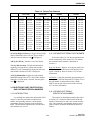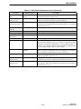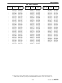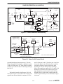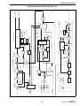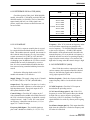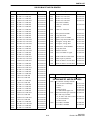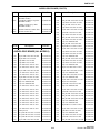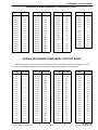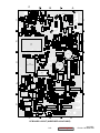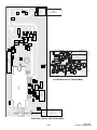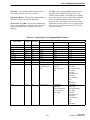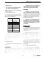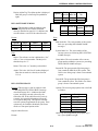
1
SERVICE
MANUAL
LTR ® MOBILE
984X SERIES (UHF)
988X SERIES (800 MHZ)
989X SERIES (900 MHZ)
98XX SERIES (DATA)
LTR MOBILE
®
25 or 40 Watts (UHF); 15 or 30 Watts (800/900 MHz)
13.6 VDC
Part No. 242-98xx-2xx
High Tier
Low Tier
Remote-Mount
High-Tier
Second Issue
April 2001
Supersedes: Part No. 001-9800-200; 9/99
98xx-SERIES
FM TWO-WAY RADIO
SERVICE MANUAL
13.6 VDC
25 or 40 Watts, UHF
15 or 30 Watts, 800/900 MHz
Part No. 242-984x-2xx (UHF)
Part No. 242-988x-2xx (800 MHz)
Part No. 242-989x-2xx (900 MHz)
Copyright © 2001by the E.F. Johnson Company
The E.F. Johnson Company, which was founded in 1923, provides wireless communication
systems solutions for public safety, government, and commercial customers. The company
designs, manufactures, and markets conventional and trunked radio systems, mobile and
portable subscriber radios, repeaters, and Project 25 digital radio products.
Viking Head/EFJohnson logo, LTR®, LTR-Net™, Multi-Net®, and Call Guard® are trademarks
of the E.F. Johnson Company. SMARTNET™ and SmartZone® are trademarks of Motorola,
Inc. All other company and/or product names used in this manual are trademarks and/or registered trademarks of their respective manufacturer.
Information in this manual is subject to change without notice.
TABLE OF CONTENTS
TABLE OF CONTENTS
1
GENERAL INFORMATION
3
OPERATION
SCOPE OF MANUAL . . . . . . . . . . . . . . . . . . . . 1-1
TRANSCEIVER DESCRIPTION . . . . . . . . . . .1-1
General . . . . . . . . . . . . . . . . . . . . . . . . . . . . . . . . 1-1
Available Frequency Bands . . . . . . . . . . . . . . . . 1-1
Low And High Tier Models . . . . . . . . . . . . . . . . 1-1
Data Models . . . . . . . . . . . . . . . . . . . . . . . . . . . . 1-2
Front and Remote Mounting . . . . . . . . . . . . . . . 1-2
NPSPAC Models (800 MHz Only) . . . . . . . . . . 1-2
Programming . . . . . . . . . . . . . . . . . . . . . . . . . . . 1-3
Transceiver Alignment . . . . . . . . . . . . . . . . . . . . 1-3
1.3
PART NUMBER BREAKDOWN . . . . . . . . . . .1-3
1.4
TRANSCEIVER IDENTIFICATION . . . . . . . .1-3
1.5
ACCESSORIES . . . . . . . . . . . . . . . . . . . . . . . . . 1-4
1.6
PRODUCT WARRANTY . . . . . . . . . . . . . . . . . 1-5
1.7
FACTORY CUSTOMER SERVICE . . . . . . . .1-5
1.8
FACTORY RETURNS . . . . . . . . . . . . . . . . . . .1-6
1.9
REPLACEMENT PARTS . . . . . . . . . . . . . . . . . 1-6
1.10 INTERNET HOME PAGE . . . . . . . . . . . . . . . . . 1-6
3.1
3.2
UHF 984x SPECIFICATIONS . . . . . . . . . 1-7
800 MHz 988x SPECIFICATIONS . . . . . 1-8
900 MHz 989x SPECIFICATIONS . . . . . 1-9
3.5
FEATURES . . . . . . . . . . . . . . . . . . . . . . . . . . . . 3-1
CONTROLS. . . . . . . . . . . . . . . . . . . . . . . . . . . . 3-3
Low Tier Controls . . . . . . . . . . . . . . . . . . . . . . . . 3-3
High Tier Controls and Indicator . . . . . . . . . . . . 3-3
Rear Panel Jacks and Connectors . . . . . . . . . . . . 3-4
DISPLAY DESCRIPTION . . . . . . . . . . . . . . . . 3-4
Low Tier Display. . . . . . . . . . . . . . . . . . . . . . . . . 3-4
High Tier Display . . . . . . . . . . . . . . . . . . . . . . . . 3-5
GENERAL OPERATION. . . . . . . . . . . . . . . . . 3-5
Power-Up Sequence . . . . . . . . . . . . . . . . . . . . . . 3-5
Determining Volume Level. . . . . . . . . . . . . . . . . 3-5
Backlight Operation . . . . . . . . . . . . . . . . . . . . . . 3-6
System/Group Display Information . . . . . . . . . . 3-6
Selecting Systems And Groups . . . . . . . . . . . . . . 3-6
Setting Squelch Control. . . . . . . . . . . . . . . . . . . . 3-7
LTR and Conventional Operating Modes . . . . . . 3-8
Placing and Receiving Standard (Dispatch) Calls 3-9
Placing and Receiving Telephone Calls . . . . . . . 3-9
GENERAL FEATURES . . . . . . . . . . . . . . . . . 3-10
AUX (Auxiliary) Switch(es) . . . . . . . . . . . . . . . 3-10
Bank Select (High Tier Only) . . . . . . . . . . . . . . 3-10
Call Indicator . . . . . . . . . . . . . . . . . . . . . . . . . . . 3-10
Companding . . . . . . . . . . . . . . . . . . . . . . . . . . . 3-11
Data System/Groups . . . . . . . . . . . . . . . . . . . . . 3-11
Emergency Switch (High Tier Only) . . . . . . . . 3-11
Encryption . . . . . . . . . . . . . . . . . . . . . . . . . . . . . 3-11
Function Switch (High Tier Only) . . . . . . . . . . 3-12
Home System/Group Select . . . . . . . . . . . . . . . 3-12
Horn Alert . . . . . . . . . . . . . . . . . . . . . . . . . . . . . 3-12
Option Select . . . . . . . . . . . . . . . . . . . . . . . . . . . 3-13
Power Turn-Off Delay. . . . . . . . . . . . . . . . . . . . 3-13
Proceed (Clear-To-Talk) Tone . . . . . . . . . . . . . 3-14
Programmable Power Output . . . . . . . . . . . . . . 3-14
Stealth Mode (High Tier Only) . . . . . . . . . . . . . 3-14
Time-Out Timer . . . . . . . . . . . . . . . . . . . . . . . . 3-14
Tone Select . . . . . . . . . . . . . . . . . . . . . . . . . . . . 3-15
Transmitter Thermal Foldback . . . . . . . . . . . . . 3-15
OPTION SWITCHES AND MENU MODE . 3-15
Using Option Switches . . . . . . . . . . . . . . . . . . . 3-15
Using Menu Mode. . . . . . . . . . . . . . . . . . . . . . . 3-15
Using Menu Mode. . . . . . . . . . . . . . . . . . . . . . . 3-17
A/D (Scan List Programming) . . . . . . . . . . . . . 3-17
Backlight Adjust . . . . . . . . . . . . . . . . . . . . . . . . 3-17
Bank Select . . . . . . . . . . . . . . . . . . . . . . . . . . . . 3-17
Call Guard Squelch Disable . . . . . . . . . . . . . . . 3-17
Emergency Switch. . . . . . . . . . . . . . . . . . . . . . . 3-17
Encryption On-Off . . . . . . . . . . . . . . . . . . . . . . 3-17
Function Select (High Tier Models) . . . . . . . . . 3-18
Home System/Group Select . . . . . . . . . . . . . . . 3-18
Horn Alert . . . . . . . . . . . . . . . . . . . . . . . . . . . . . 3-18
LTR System Search Select . . . . . . . . . . . . . . . . 3-18
1.1
1.2
2
INSTALLATION
2.1
GENERAL. . . . . . . . . . . . . . . . . . . . . . . . . . . . . . 2-1
Scope of Instructions . . . . . . . . . . . . . . . . . . . . . 2-1
Performance Tests . . . . . . . . . . . . . . . . . . . . . . . 2-1
Transceiver Programming . . . . . . . . . . . . . . . . . 2-2
Required Power Source . . . . . . . . . . . . . . . . . . . 2-2
MOUNTING THE TRANSCEIVER . . . . . . . . . 2-2
Selecting A Mounting Location . . . . . . . . . . . . . 2-2
Installation Components . . . . . . . . . . . . . . . . . . . 2-2
Attaching Mounting Bracket . . . . . . . . . . . . . . . 2-2
POWER CABLE INSTALLATION . . . . . . . . . 2-3
ACCESSORY CABLE INSTALLATION . . . . 2-4
General . . . . . . . . . . . . . . . . . . . . . . . . . . . . . . . . 2-4
Accessory Pigtail Installation . . . . . . . . . . . . . . . 2-5
Connecting Ignition Sense Wire. . . . . . . . . . . . . 2-5
Connecting Horn Alert Wire . . . . . . . . . . . . . . . 2-6
Other Accessory Cable Outputs . . . . . . . . . . . . . 2-6
REMOTE CONTROL UNIT INSTALLATION 2-6
General . . . . . . . . . . . . . . . . . . . . . . . . . . . . . . . . 2-6
Mounting Remote Control Unit . . . . . . . . . . . . . 2-6
USING AN EXTERNAL SPEAKER . . . . . . . . 2-7
DATA CABLE INSTALLATION . . . . . . . . . . . 2-7
General . . . . . . . . . . . . . . . . . . . . . . . . . . . . . . . . 2-8
Data Cable Installation . . . . . . . . . . . . . . . . . . . . 2-8
KEY CAP KITS . . . . . . . . . . . . . . . . . . . . . . . . . 2-8
2.2
2.3
2.4
2.5
2.6
2.7
2.8
3.3
3.4
3.6
ii
February 2001
Part No. 001-9800-001
TABLE OF CONTENTS
TABLE OF CONTENTS (CONT’D)
3.12 ELECTRONIC PART, IDENTIFICATION, AND
SOFTWARE VERSION NUMBERS . . . . 3-37
Introduction . . . . . . . . . . . . . . . . . . . . . . . . . . . . 3-37
Viewing Electronic Part Number . . . . . . . . . . . 3-37
Viewing Electronic Identification Number . . . . 3-38
Viewing Software Version Number . . . . . . . . . 3-38
Menu Mode Select . . . . . . . . . . . . . . . . . . . . . . 3-18
Monitor Mode Select . . . . . . . . . . . . . . . . . . . . 3-18
Option Select . . . . . . . . . . . . . . . . . . . . . . . . . . 3-18
Priority Sampling Select. . . . . . . . . . . . . . . . . . 3-18
Scan On-Off . . . . . . . . . . . . . . . . . . . . . . . . . . . 3-18
Scan Type Select . . . . . . . . . . . . . . . . . . . . . . . 3-18
Scan Continue Select . . . . . . . . . . . . . . . . . . . . 3-18
Scan List Save Mode . . . . . . . . . . . . . . . . . . . . 3-19
Stealth Mode Select . . . . . . . . . . . . . . . . . . . . . 3-19
Squelch Adjust . . . . . . . . . . . . . . . . . . . . . . . . . 3-19
System/Group Display Mode . . . . . . . . . . . . . . 3-19
Talk-Around Select . . . . . . . . . . . . . . . . . . . . . 3-19
Tone Type Select . . . . . . . . . . . . . . . . . . . . . . . 3-19
3.7
SYSTEM AND GROUP SCAN . . . . . . . . . . . 3-19
General . . . . . . . . . . . . . . . . . . . . . . . . . . . . . . . 3-19
Scan List Programming . . . . . . . . . . . . . . . . . . 3-20
Scan Delay and Continue Timers . . . . . . . . . . . 3-21
Transmitting In The Scan Mode. . . . . . . . . . . . 3-22
Fixed Transmit In Scan . . . . . . . . . . . . . . . . . . 3-22
Scanning LTR Systems . . . . . . . . . . . . . . . . . . 3-23
Scanning Conventional Systems . . . . . . . . . . . 3-23
3.8
LTR FEATURES . . . . . . . . . . . . . . . . . . . . . . . 3-23
Systems. . . . . . . . . . . . . . . . . . . . . . . . . . . . . . . 3-23
Groups . . . . . . . . . . . . . . . . . . . . . . . . . . . . . . . 3-23
Receive Priority ID Codes . . . . . . . . . . . . . . . . 3-24
LTR Standard Calls . . . . . . . . . . . . . . . . . . . . . 3-24
LTR Telephone Calls . . . . . . . . . . . . . . . . . . . . 3-25
Transmit Inhibit . . . . . . . . . . . . . . . . . . . . . . . . 3-26
Busy Queuing . . . . . . . . . . . . . . . . . . . . . . . . . . 3-26
System Search . . . . . . . . . . . . . . . . . . . . . . . . . 3-27
Transpond . . . . . . . . . . . . . . . . . . . . . . . . . . . . . 3-27
3.9
CONVENTIONAL MODE FEATURES . . . .3-27
Monitor Mode. . . . . . . . . . . . . . . . . . . . . . . . . . 3-27
Transmit Disable On Busy . . . . . . . . . . . . . . . . 3-27
Receive-Only Groups . . . . . . . . . . . . . . . . . . . . 3-28
Talk-Around . . . . . . . . . . . . . . . . . . . . . . . . . . . 3-28
Call Guard Squelch. . . . . . . . . . . . . . . . . . . . . . 3-28
Priority Group Sampling . . . . . . . . . . . . . . . . . 3-29
External Encoders and Decoders . . . . . . . . . . . 3-30
3.10 SUPERVISORY TONES AND DISPLAY
MESSAGES . . . . . . . . . . . . . . . . . . . . . . . . . 3-31
General Tones. . . . . . . . . . . . . . . . . . . . . . . . . . 3-31
LTR Telephone Call Tones . . . . . . . . . . . . . . . 3-32
Display Messages . . . . . . . . . . . . . . . . . . . . . . . 3-32
Menu Mode Messages (High Tier Only) . . . . . 3-33
3.11 TEST MODE . . . . . . . . . . . . . . . . . . . . . . . . . . .3-34
High Tier Option Switch Identification . . . . . . 3-34
Entering Test Mode . . . . . . . . . . . . . . . . . . . . . 3-34
Exiting Test Mode . . . . . . . . . . . . . . . . . . . . . . 3-35
Test Mode Default Conditions . . . . . . . . . . . . . 3-35
Test Channel Selection . . . . . . . . . . . . . . . . . . . 3-35
Modulation Selection . . . . . . . . . . . . . . . . . . . . 3-35
Miscellaneous . . . . . . . . . . . . . . . . . . . . . . . . . . 3-35
4
PROGRAMMING
4.1
GENERAL . . . . . . . . . . . . . . . . . . . . . . . . . . . . . 4-1
Programming Setup. . . . . . . . . . . . . . . . . . . . . . . 4-1
Minimum Computer Requirements. . . . . . . . . . . 4-1
RPI Cables. . . . . . . . . . . . . . . . . . . . . . . . . . . . . . 4-2
Remote Programming Interface (RPI) . . . . . . . . 4-2
EEPROM Data Storage . . . . . . . . . . . . . . . . . . . . 4-2
Hardware Hookup . . . . . . . . . . . . . . . . . . . . . . . . 4-2
Powering Up a Data Transceiver. . . . . . . . . . . . . 4-2
SOFTWARE INSTALLATION
INFORMATION . . . . . . . . . . . . . . . . . . . . . . . 4-3
General . . . . . . . . . . . . . . . . . . . . . . . . . . . . . . . . 4-3
Minimum Free Memory Required . . . . . . . . . . . 4-3
Software Installation . . . . . . . . . . . . . . . . . . . . . . 4-3
Starting The Program . . . . . . . . . . . . . . . . . . . . . 4-4
MISCELLANEOUS PROGRAM
INFORMATION . . . . . . . . . . . . . . . . . . . . . . . 4-4
Header Information . . . . . . . . . . . . . . . . . . . . . . . 4-4
Special Keys . . . . . . . . . . . . . . . . . . . . . . . . . . . . 4-5
PROGRAMMING PROCEDURE . . . . . . . . . . 4-5
MAIN MENU . . . . . . . . . . . . . . . . . . . . . . . . . . . 4-8
Introduction . . . . . . . . . . . . . . . . . . . . . . . . . . . . . 4-8
Set Up New Configuration File. . . . . . . . . . . . . . 4-8
Open Configuration File . . . . . . . . . . . . . . . . . . . 4-8
Modify Current Configuration File . . . . . . . . . . . 4-9
Upload Configuration From Radio . . . . . . . . . . . 4-9
Download Configuration To Radio. . . . . . . . . . . 4-9
Print Current Configuration File . . . . . . . . . . . . . 4-9
Modify Printer/Serial Ports . . . . . . . . . . . . . . . . . 4-9
Configuration File Utilities . . . . . . . . . . . . . . . . 4-10
MODIFY RADIO FILE MENU . . . . . . . . . . . . 4-10
Introduction . . . . . . . . . . . . . . . . . . . . . . . . . . . . 4-10
Edit Main Radio Parameters . . . . . . . . . . . . . . . 4-10
Define Option Buttons. . . . . . . . . . . . . . . . . . . . 4-12
Setup Menu Functions. . . . . . . . . . . . . . . . . . . . 4-12
Create/Edit/Copy/Delete System. . . . . . . . . . . . 4-12
Create/Edit/Delete Bank . . . . . . . . . . . . . . . . . . 4-14
Setup Prestored Numbers . . . . . . . . . . . . . . . . . 4-15
Setup/Change Unique ID. . . . . . . . . . . . . . . . . . 4-16
Change Model/Band/Range/Tier. . . . . . . . . . . . 4-16
ADDITIONAL PROGRAMMING
INFORMATION . . . . . . . . . . . . . . . . . . . . . . 4-16
Repeater Number Programming . . . . . . . . . . . . 4-16
Channel Number Programming. . . . . . . . . . . . . 4-16
Specifying RIC-Equipped Repeaters. . . . . . . . . 4-16
4.2
4.3
4.4
4.5
4.6
4.7
iii
February 2001
Part No. 001-9800-001
TABLE OF CONTENTS
TABLE OF CONTENTS (CONT’D)
4.8
4.9
UPDATING RADIO SOFTWARE . . . . . . . . . 4-16
Introduction . . . . . . . . . . . . . . . . . . . . . . . . . . . 4-16
Data File . . . . . . . . . . . . . . . . . . . . . . . . . . . . . . 4-17
I/O LINE PROGRAMMING . . . . . . . . . . . . . . 4-17
Introduction . . . . . . . . . . . . . . . . . . . . . . . . . . . 4-17
Transceiver and Programming Software
Required . . . . . . . . . . . . . . . . . . . . . . . . . . . . 4-18
Programming For Options . . . . . . . . . . . . . . . . 4-18
Programming I/O Interface Options . . . . . . . . . 4-18
5
CIRCUIT DESCRIPTION
5.1
GENERAL TRANSCEIVER DESCRIPTION 5-1
Introduction . . . . . . . . . . . . . . . . . . . . . . . . . . . . 5-1
Circuit Protection (Fuses). . . . . . . . . . . . . . . . . . 5-1
Synthesizer . . . . . . . . . . . . . . . . . . . . . . . . . . . . . 5-1
Audio/Logic Board . . . . . . . . . . . . . . . . . . . . . . . 5-1
Receiver . . . . . . . . . . . . . . . . . . . . . . . . . . . . . . . 5-2
Transmitter . . . . . . . . . . . . . . . . . . . . . . . . . . . . . 5-2
POWER DISTRIBUTION AND SWITCHING 5-2
Power Switching Control . . . . . . . . . . . . . . . . . . 5-2
Supply Switching . . . . . . . . . . . . . . . . . . . . . . . . 5-2
AUDIO/LOGIC BOARD DIGITAL CIRCUIT . 5-4
Microcontroller (U101) . . . . . . . . . . . . . . . . . . . 5-4
Memory and Latch Programming . . . . . . . . . . . 5-6
RECEIVE AUDIO/DATA PROCESSING. . . . 5-7
Amplifier (U301B) . . . . . . . . . . . . . . . . . . . . . . . 5-7
Receive Audio Processing . . . . . . . . . . . . . . . . . 5-8
Receive Data Processing . . . . . . . . . . . . . . . . . . 5-9
Squelch Circuit (U304A, U304B) . . . . . . . . . . . 5-9
TRANSMIT AUDIO/DATA PROCESSING . 5-10
Microphone Amplifier (U303B), High-Pass
Filter (U303C) . . . . . . . . . . . . . . . . . . . . . . . 5-10
Summing Amplifier (U303D), Pre-Emphasis/
Limiter (U303A) . . . . . . . . . . . . . . . . . . . . . 5-10
Splatter Filter (U302B, U302C) . . . . . . . . . . . . 5-10
Transmit Data Circuit (U302D, U302A) . . . . . 5-11
DISPLAY BOARDS . . . . . . . . . . . . . . . . . . . . 5-11
SYNTHESIZER CIRCUIT DESCRIPTION
(UHF MODELS) . . . . . . . . . . . . . . . . . . . . . . 5-12
Introduction . . . . . . . . . . . . . . . . . . . . . . . . . . . 5-12
Voltage-Controlled Oscillator . . . . . . . . . . . . . 5-12
Active Filter (Q800), Buffer Amplifier (Q801) 5-14
VCO and TCXO Modulation . . . . . . . . . . . . . . 5-15
Synthesizer Integrated Circuit (U804) . . . . . . . 5-15
Lock Detect . . . . . . . . . . . . . . . . . . . . . . . . . . . 5-17
Charge Pump . . . . . . . . . . . . . . . . . . . . . . . . . . 5-17
Shift Register (U800, U801) and Digital
Potentiometer (U802) Programming . . . . . . 5-17
RECEIVER CIRCUIT DESCRIPTION (UHF
MODELS) . . . . . . . . . . . . . . . . . . . . . . . . . . . . 5-17
Front End Filter . . . . . . . . . . . . . . . . . . . . . . . . 5-17
RF Amplifier (Q201) . . . . . . . . . . . . . . . . . . . . 5-18
5.2
5.3
5.4
5.5
5.6
5.7
5.8
First Mixer (Q202), Injection Amplifier (Q204) 5-18
Second Mixer/Detector (U201) . . . . . . . . . . . . . 5-18
5.9
TRANSMITTER CIRCUIT DESCRIPTION
(UHF MODELS) . . . . . . . . . . . . . . . . . . . . . . 5-19
First and Second Amplifiers . . . . . . . . . . . . . . . 5-19
Third Amp and Predriver . . . . . . . . . . . . . . . . . 5-20
Driver (Q600), Final (Q601) . . . . . . . . . . . . . . . 5-21
Antenna Switch . . . . . . . . . . . . . . . . . . . . . . . . . 5-21
Directional Coupler, Low-Pass Filter . . . . . . . . 5-21
Power Control (U500A/B, Q500-Q503) . . . . . . 5-22
5.10 SYNTHESIZER CIRCUIT DESCRIPTION
(800/900 MHz MODELS) . . . . . . . . . . . . . . 5-24
Introduction . . . . . . . . . . . . . . . . . . . . . . . . . . . . 5-24
Voltage-Controlled Oscillator . . . . . . . . . . . . . . 5-24
VCO and TCXO Modulation . . . . . . . . . . . . . . 5-25
Active Filter (Q800) . . . . . . . . . . . . . . . . . . . . . 5-26
Buffer Amplifier (Q801), Tx/Tx Switch
(CR801/CR802) . . . . . . . . . . . . . . . . . . . . . . 5-26
Synthesizer Integrated Circuit (U804) . . . . . . . 5-27
Lock Detect . . . . . . . . . . . . . . . . . . . . . . . . . . . . 5-28
Charge Pump . . . . . . . . . . . . . . . . . . . . . . . . . . . 5-28
Shift Register (U800, U801) and Digital
Potentiometer (U802) Programming. . . . . . . 5-28
5.11 RECEIVER CIRCUIT DESCRIPTION
(800/900 MHz MODELS) . . . . . . . . . . . . . . 5-28
Front End Filter . . . . . . . . . . . . . . . . . . . . . . . . . 5-28
RF Amplifier (Q201). . . . . . . . . . . . . . . . . . . . . 5-28
First Mixer (Q202), Crystal Filter (Z204) . . . . . 5-29
Second Mixer/Detector (U201) . . . . . . . . . . . . . 5-29
5.12 TRANSMITTER CIRCUIT DESCRIPTION
(800/900 MHz MODELS) . . . . . . . . . . . . . . 5-30
Predriver (Q506), Driver (Q507). . . . . . . . . . . . 5-30
Power Amplifier Module (U600), Final (Q651) 5-31
Antenna Switch . . . . . . . . . . . . . . . . . . . . . . . . . 5-31
Directional Coupler, Low-Pass Filter . . . . . . . . 5-31
Power Control (U500A/B, Q500-Q503) . . . . . . 5-32
6
SERVICING
6.1
GENERAL . . . . . . . . . . . . . . . . . . . . . . . . . . . . .
Periodic Checks. . . . . . . . . . . . . . . . . . . . . . . . . .
Schematic Diagrams and Component Layouts . .
Replacement Parts . . . . . . . . . . . . . . . . . . . . . . . .
Configuring Transceiver for Testing . . . . . . . . . .
SURFACE MOUNTED DEVICES (SMDs) . .
Servicing Techniques . . . . . . . . . . . . . . . . . . . . .
Identifying SMD Resistors . . . . . . . . . . . . . . . . .
SMD Capacitor Identification . . . . . . . . . . . . . . .
SMD Inductor Identification . . . . . . . . . . . . . . . .
Transistor/Diode Identification . . . . . . . . . . . . . .
SYNTHESIZER TROUBLESHOOTING . . . .
Introduction . . . . . . . . . . . . . . . . . . . . . . . . . . . . .
Reference Oscillator (U806) . . . . . . . . . . . . . . . .
6.2
6.3
iv
6-1
6-1
6-1
6-1
6-1
6-1
6-1
6-1
6-2
6-3
6-3
6-3
6-3
6-4
February 2001
Part No. 001-9800-001
TABLE OF CONTENTS
TABLE OF CONTENTS (CONT’D)
6.4
6.5
6.6
VCO Module . . . . . . . . . . . . . . . . . . . . . . . . . . . 6-4
Synthesizer IC (U804) . . . . . . . . . . . . . . . . . . . . 6-4
Determining Synthesizer Counter Divide
Numbers . . . . . . . . . . . . . . . . . . . . . . . . . . . . . 6-5
RECEIVER SERVICING . . . . . . . . . . . . . . . . . . 6-5
TRANSMITTER SERVICING . . . . . . . . . . . . . 6-5
AUDIO/LOGIC BOARD SERVICING . . . . . . . 6-5
Digital Circuits . . . . . . . . . . . . . . . . . . . . . . . . . . 6-5
Analog Circuits. . . . . . . . . . . . . . . . . . . . . . . . . . 6-5
Exploded Views
High Tier Front Panel . . . . . . . . . . . . . . . . . .
Low Tier Front Panel . . . . . . . . . . . . . . . . . .
Front And Top Mechanical Parts . . . . . . . . .
Bottom Mechanical Parts . . . . . . . . . . . . . . .
Remote Control Unit Mechanical Parts . . . .
Remote Transceiver Mechanical Parts . . . . .
9
7
ALIGNMENT PROCEDURE AND
PERFORMANCE TESTS
7.1
GENERAL. . . . . . . . . . . . . . . . . . . . . . . . . . . . . . 7-1
Introduction . . . . . . . . . . . . . . . . . . . . . . . . . . . . 7-1
Test Mode . . . . . . . . . . . . . . . . . . . . . . . . . . . . . . 7-1
Test Setup . . . . . . . . . . . . . . . . . . . . . . . . . . . . . . 7-2
USING TUNE SOFTWARE . . . . . . . . . . . . . . . 7-2
General . . . . . . . . . . . . . . . . . . . . . . . . . . . . . . . . 7-2
Installation . . . . . . . . . . . . . . . . . . . . . . . . . . . . . 7-2
Program Operation . . . . . . . . . . . . . . . . . . . . . . . 7-2
Tune Radio Screen . . . . . . . . . . . . . . . . . . . . . . . 7-3
ADJUSTMENT PROCEDURE . . . . . . . . . . . . 7-4
Preliminary . . . . . . . . . . . . . . . . . . . . . . . . . . . . . 7-4
Frequency and Bias Adjustment. . . . . . . . . . . . . 7-4
Modulation Peak Frequency (UHF Models
Only). . . . . . . . . . . . . . . . . . . . . . . . . . . . . . . . 7-4
Power Output . . . . . . . . . . . . . . . . . . . . . . . . . . . 7-4
Modulation Balance . . . . . . . . . . . . . . . . . . . . . . 7-5
Transmit Audio Limiting . . . . . . . . . . . . . . . . . . 7-5
Transmit Data Level . . . . . . . . . . . . . . . . . . . . . . 7-5
Receiver IF Adjustment . . . . . . . . . . . . . . . . . . . 7-5
Squelch Level Adjust . . . . . . . . . . . . . . . . . . . . . 7-6
RECEIVER PERFORMANCE TESTS . . . . . . 7-7
TRANSMITTER PERFORMANCE TESTS . . 7-7
Checking Power Output . . . . . . . . . . . . . . . . . . . 7-7
Checking Frequency . . . . . . . . . . . . . . . . . . . . . . 7-7
Checking Deviation . . . . . . . . . . . . . . . . . . . . . . 7-7
7.2
7.3
7.4
7.5
8
8-33
8-34
8-32
8-32
8-33
8-33
SCHEMATIC DIAGRAMS AND
COMPONENT LAYOUTS
Transistor and Diode Basing Diagrams. . . . . . . . 9-1
Amplified Dynamic Microphone . . . . . . . . . . . . 9-2
Transceiver Top Photo . . . . . . . . . . . . . . . . . . . . 9-3
Transceiver Bottom Photo. . . . . . . . . . . . . . . . . . 9-3
High Tier Interconnect Schematic. . . . . . . . . . 9-4
High Tier Interface Board Layout. . . . . . . . . . 9-4
High Tier Display Board
Top View. . . . . . . . . . . . . . . . . . . . . . . . . . . . . 9-5
Bottom View . . . . . . . . . . . . . . . . . . . . . . . . . . 9-5
RPI (P.N. 023-9800-000)
RPI (P.N. 023-9800-000) Board Layout. . . . . 9-6
Programming Cable . . . . . . . . . . . . . . . . . . . . 9-6
RPI (P.N. 023-9800-000) Schematic . . . . . . . 9-6
Component Locator Guides
RF Board (UHF) . . . . . . . . . . . . . . . . . . . . . . . 9-7
RF Board (800/900 MHz) . . . . . . . . . . . . . . . 9-10
Audio/Logic Board . . . . . . . . . . . . . . . . . . . . 9-12
PARTS LIST
Front Panel Assembly And Mechanical Parts . . 8-1
UHF RF And PA Boards . . . . . . . . . . . . . . . . . . 8-3
800/900 MHz RF And PA Boards . . . . . . . . . . 8-18
Audio/Logic Board (All Models) . . . . . . . . . . . 8-26
9800-Series Radio Mounting Kit . . . . . . . . . . . 8-31
9800-Series Remote Mounting Kit. . . . . . . . . . 8-31
DC Power Cable And Hardware Kit . . . . . . . . 8-31
Accessory Wire Kit . . . . . . . . . . . . . . . . . . . . . 8-31
Amplified Dynamic Microphone . . . . . . . . . . . 8-31
15 Watt, 4.7-Ohm Speaker (Black) . . . . . . . . . 8-32
430-470 MHz RF
RF Board Schematic (Revised). . . . . . . . . . .
PA Board Schematic (25W) . . . . . . . . . . . . .
RF Board Layout. . . . . . . . . . . . . . . . . . . . . .
VCO Board Layout . . . . . . . . . . . . . . . . . . . .
PA Board Layout (25W) . . . . . . . . . . . . . . . .
PA Board Schematic (40W) . . . . . . . . . . . . .
PA Board Layout (40W) . . . . . . . . . . . . . . . .
RF Board Schematic (Unrevised) . . . . . . . . .
RF Board Layout (Unrevised). . . . . . . . . . . .
9-15
9-15
9-16
9-17
9-17
9-18
9-19
9-20
9-21
470-512 MHz RF
RF Board Schematic . . . . . . . . . . . . . . . . . . .
PA Board Schematic (25W) . . . . . . . . . . . . .
RF Board Layout . . . . . . . . . . . . . . . . . . . . .
VCO Board Layout . . . . . . . . . . . . . . . . . . . .
PA Board Layout (25W) . . . . . . . . . . . . . . . .
PA Board Schematic (40W) . . . . . . . . . . . . .
PA Board Layout (40W) . . . . . . . . . . . . . . . .
9-22
9-22
9-23
9-24
9-24
9-25
9-26
800/900 MHz RF
RF Board Schematic . . . . . . . . . . . . . . . . . . . 9-27
PA Board Schematic (15W) . . . . . . . . . . . . . 9-27
v
February 2001
Part No. 001-9800-001
TABLE OF CONTENTS
TABLE OF CONTENTS (CONT’D)
9-28
9-29
9-30
9-30
9-31
9-32
B.4
High Tier Audio/Logic Board
Schematic . . . . . . . . . . . . . . . . . . . . . . . . . . . 9-33
Board Layout . . . . . . . . . . . . . . . . . . . . . . . . 9-34
B.6
Low Tier Interconnect and Display Boards
Display Board (Back View) . . . . . . . . . . . . . 9-35
Interconnect Schematic . . . . . . . . . . . . . . . . 9-36
C
REVISION SUMMARY
C.1
C.2
C.3
C.4
OPERATING SOFTWARE REVISIONS . . . C-1
PROGRAMMING SOFTWARE REVISIONS C-1
TUNING SOFTWARE REVISIONS . . . . . . . . C-2
REVISION LETTER CHANGES . . . . . . . . . . C-2
General . . . . . . . . . . . . . . . . . . . . . . . . . . . . . . . C-2
Squelch Change. . . . . . . . . . . . . . . . . . . . . . . . . C-2
LTR-Net Upgradable Models . . . . . . . . . . . . . . C-2
ADDITIONAL CHANGES MADE SINCE
LAST PRINTING . . . . . . . . . . . . . . . . . . . . . . C-3
RF Board Layout (800 MHz) . . . . . . . . . . . .
RF Board Layout (900 MHz) . . . . . . . . . . . .
VCO Board Layout . . . . . . . . . . . . . . . . . . .
PA Board Layout (15W) . . . . . . . . . . . . . . .
PA Board Schematic (30W). . . . . . . . . . . . .
PA Board Layout (30W) . . . . . . . . . . . . . . .
B.5
Low Tier/Data Only Audio/Logic Board
Board Layout . . . . . . . . . . . . . . . . . . . . . . . . 9-37
Schematic . . . . . . . . . . . . . . . . . . . . . . . . . . . 9-38
A
DATA INTERFACE DESCRIPTION
A.1
GENERAL INFORMATION . . . . . . . . . . . . . .
Introduction . . . . . . . . . . . . . . . . . . . . . . . . . . . .
Software Version Required . . . . . . . . . . . . . . . .
ELECTRICAL SPECIFICATIONS . . . . . . . .
SIGNAL FUNCTIONS . . . . . . . . . . . . . . . . . . .
Introduction . . . . . . . . . . . . . . . . . . . . . . . . . . . .
Definitions . . . . . . . . . . . . . . . . . . . . . . . . . . . . .
Input Functions . . . . . . . . . . . . . . . . . . . . . . . . . .
Output Functions . . . . . . . . . . . . . . . . . . . . . . . .
DATA MODEM OPERATION . . . . . . . . . . . .
Data Group Support . . . . . . . . . . . . . . . . . . . . . .
Data ARQ Mode. . . . . . . . . . . . . . . . . . . . . . . . .
C.5
A.2
A.3
A.4
A-1
A-1
A-1
A-1
A-3
A-3
A-3
A-3
A-4
A-8
A-8
A-8
B
EXTERNAL SERIAL CONTROL
PROTOCOL
B.1
INTRODUCTION . . . . . . . . . . . . . . . . . . . . . . . B-1
Goals of This Protocol . . . . . . . . . . . . . . . . . . . . B-1
Protocol Layers. . . . . . . . . . . . . . . . . . . . . . . . . . B-1
MESSAGE FRAMING AND FORMATTING B-1
Frame Format . . . . . . . . . . . . . . . . . . . . . . . . . . . B-1
Frame Encoding/Decoding Examples . . . . . . . . B-2
Frame Addressing. . . . . . . . . . . . . . . . . . . . . . . . B-4
Frame Types . . . . . . . . . . . . . . . . . . . . . . . . . . . . B-4
Frame Acknowledgment . . . . . . . . . . . . . . . . . . B-4
Packet Collision . . . . . . . . . . . . . . . . . . . . . . . . . B-5
Error Handling . . . . . . . . . . . . . . . . . . . . . . . . . . B-6
Multiple Frame Support . . . . . . . . . . . . . . . . . . . B-6
UNREGISTERED MODE . . . . . . . . . . . . . . . . B-6
Introduction . . . . . . . . . . . . . . . . . . . . . . . . . . . . B-6
Message Formats . . . . . . . . . . . . . . . . . . . . . . . . B-7
B.2
B.3
POWER DOWN MODE . . . . . . . . . . . . . . . . . . B-8
Introduction . . . . . . . . . . . . . . . . . . . . . . . . . . . . B-8
Message Formats. . . . . . . . . . . . . . . . . . . . . . . . B-8
STANDARD COMMAND MODE . . . . . . . . . B-10
Introduction . . . . . . . . . . . . . . . . . . . . . . . . . . . B-10
User Interface Messages . . . . . . . . . . . . . . . . . B-10
Operational Control Messages . . . . . . . . . . . . B-21
REMOTE COMMAND MODE . . . . . . . . . . . B-25
Introduction . . . . . . . . . . . . . . . . . . . . . . . . . . . B-25
Command Messages . . . . . . . . . . . . . . . . . . . . B-26
LIST OF TABLES
1-1
1-3
1-2
2-1
3-1
3-2
3-3
3-4
4-1
4-2
4-3
4-4
4-5
6-1
6-2
A-1
A-2
B-1
B-2
B-3
B-4
B-5
B-6
C-1
vi
Part Number Breakdown . . . . . . . . . . . . . . . . . . 1-3
98xx Accessories . . . . . . . . . . . . . . . . . . . . . . . . 1-4
Identification Number Breakdown . . . . . . . . . . . 1-4
Data Cable Wire Chart . . . . . . . . . . . . . . . . . . . . 2-8
Low and High Tier Features . . . . . . . . . . . . . . . . 3-2
Menu Mode and Option Switch Functions . . . . 3-16
Test Mode Modulation Schemes . . . . . . . . . . . 3-35
Default Test Channels . . . . . . . . . . . . . . . . . . . 3-36
Main Radio Parameters Screen . . . . . . . . . . . . 4-19
Create/Edit Bank Parameters Screen . . . . . . . . 4-21
LTR System Parameters . . . . . . . . . . . . . . . . . . 4-22
Conventional System Parameters . . . . . . . . . . . 4-25
Call Guard Codes and Tones . . . . . . . . . . . . . . 4-28
Ceramic SMD Capacitor Identification . . . . . . . 6-2
SMD Inductor Identification . . . . . . . . . . . . . . . 6-3
Data Interface Line Electrical Specifications . . . A-1
Input/Output Line Programmable Functions . . . A-5
Control Character Replacement Index . . . . . . . . B-1
Message Format . . . . . . . . . . . . . . . . . . . . . . . . . B-2
Opcode Summary . . . . . . . . . . . . . . . . . . . . . . . . B-3
Command UI Notifications Flags . . . . . . . . . . . B-12
Info Radio StatuS Conditions . . . . . . . . . . . . . . B-24
Command Remote Notifications Flags . . . . . . B-27
Revision Letter of Upgraded Models . . . . . . . . . C-2
February 2001
Part No. 001-9800-001
TABLE OF CONTENTS
TABLE OF CONTENTS (CONT’D)
LIST OF FIGURES
1-1
2-1
2-2
2-3
2-4
2-5
2-6
3-1
3-2
3-3
3-4
4-1
4-2
4-3
4-4
4-5
4-6
4-7
5-1
5-2
5-3
5-4
5-5
5-6
5-7
6-1
7-1
7-2
7-3
7-4
B-1
B-2
B-3
B-4
B-5
Data Transceiver. . . . . . . . . . . . . . . . . . . . . . . . . 1-2
Front Mount Installation Components . . . . . . . . 2-1
Remote Mount Installation Components . . . . . . 2-3
Accessory Cable Installation . . . . . . . . . . . . . . . 2-4
Accessory Cable Connector . . . . . . . . . . . . . . . . 2-5
R170 Location Diagram . . . . . . . . . . . . . . . . . . . 2-5
Data Cable Installation (-001 Cable Shown) . . . 2-7
Frt Panel Controls and Indicators (Low-Tier) . . 3-1
Front Panel Controls and Indicators (High-Tier) 3-1
Low Tier Display and Indicators . . . . . . . . . . . . 3-4
High Tier Display . . . . . . . . . . . . . . . . . . . . . . . . 3-5
Programming Setup . . . . . . . . . . . . . . . . . . . . . . 4-1
Main Menu . . . . . . . . . . . . . . . . . . . . . . . . . . . . . 4-7
Modify Radio File Screen . . . . . . . . . . . . . . . . 4-11
Define Option Buttons Screen . . . . . . . . . . . . . 4-13
Setup Menu Functions Screen . . . . . . . . . . . . . 4-13
Channel Display Screen (Low Tier Only) . . . . 4-15
I/O Interface Options Screen . . . . . . . . . . . . . . 4-17
Power Distribution and Switching . . . . . . . . . . . 5-3
Power On-Off Control Circuit . . . . . . . . . . . . . . 5-3
Audio/Data Processing Circuitry Block Diagram 5-8
RF Block Diagram (UHF Models) . . . . . . . . . . 5-13
Synthesizer Chip U804 Block Diagram . . . . . . 5-16
Limiter/Detector U201 Block Diagram . . . . . . 5-19
RF Block Diagram (800/900 MHz Models). . . 5-23
Simplified Synthesizer Block Diagram . . . . . . . 6-3
Alignment Setup . . . . . . . . . . . . . . . . . . . . . . . . . 7-1
Tune Program Opening Screen. . . . . . . . . . . . . . 7-3
Radio Tuner Menu . . . . . . . . . . . . . . . . . . . . . . . 7-3
Alignment Points Diagram . . . . . . . . . . . . . . . . . 7-5
Ext Device Access To Subscriber Logic Cntrlr B-6
Power-Down Request Accepted. . . . . . . . . . . . B-9
Broadcast Power-Down . . . . . . . . . . . . . . . . . . B-9
Power-Down Request Denied . . . . . . . . . . . . . B-9
Addressed Power-Off . . . . . . . . . . . . . . . . . . . . B-9
vii
February 2001
Part No. 001-9800-001
GENERAL INFORMATION
SECTION 1 GENERAL INFORMATION
1.1 SCOPE OF MANUAL
800 MHz Models
This service manual contains installation, operation, programming, alignment, and service information
for E.F. Johnson LTR® 984x UHF, 988x 800 MHz,
and 989x 900 MHz transceivers. Information is
included for low and high tier versions of these transceivers, and also for both UHF frequency bands (430470 and 470-512 MHz).
•
Full band (806-824 MHz) operation.
•
All currently available models are dual bandwidth
(12.5/25 kHz).
•
High power (30W) and medium power (15W)
models available.
This manual replaces Part No. 001-9800-200 and
the -201/-202 revisions, and Part No.s 001-9880-200
and 001-9840-203. However, the -9800- manuals do
not cover discontinued mid tier models or early unrevised boards, so you may want to retain your copies of
the -9880- or -9840- manuals for that information.
900 MHz Models
In addition, this manual does not cover operation, programming, and alignment of LTR-Net™,
SMARTNET™, or SmartZone® 98xx models. It also
does not cover operation and programming of MultNet® models. This information is located in other
manuals.
•
Full band (896-902 MHz) operation.
•
Only narrow band (12.5 kHz) models are available
because the 900 MHz band has always had a 12.5
kHz channel spacing.
•
High power (30W) and medium power (15W)
models available.
1.2.3 LOW AND HIGH TIER MODELS
Each UHF, 800 MHz, or 900 MHz model is available in a low or high tier version. The tier determines
operating features, and the highlights of each tier are
as follows. Refer to Section 3.1 for more information
on the operating features.
1.2 TRANSCEIVER DESCRIPTION
1.2.1 GENERAL
The 98xx-series transceivers combine the latest
two-way radio features and technology into a rugged
and dependable package for the business, industrial,
and public safety markets. These transceivers are digitally synthesized, microcomputer-controlled, and field
programmable. All LTR models can be programmed
for both LTR and conventional operation.
NOTE: Mid tier models are no longer available. For
information on mid tier features, see Section 1.1.
Low Tier Models
•
Up to 16 system/group combinations (channels)
programmable. These combinations can be
programmed from up to 16 systems with up to 16
groups each.
•
A 1.5-digit LED type display indicates the selected
system/group combination (channel) from 1-16.
1.2.2 AVAILABLE FREQUENCY BANDS
UHF Models
•
430-470 MHz or 470-512 MHz models available.
•
All currently available models are dual bandwidth
(12.5/25 kHz). Therefore, they can be programmed
to operate on both types of channels.
•
Each system/group combination can be scanned and
the scan list is programmable. Group-only scanning
is not available.
•
High power (40W) or medium power (25W) models
available.
•
The front panel and logic board assemblies are
unique to this model.
1-1
April 2001
Part No. 001-9800-203
GENERAL INFORMATION
•
Same specifications as high tier models.
conventional or LTR systems and group IDs can be
programmed, and scanning can be used to prevent
missed calls.
High Tier Models
•
Up to 100 systems are programmable, and each
system can be programmed with up to 16 groups.
However, because of memory limitations, it is not
possible to program 100 16-group systems. The
total number of systems that can be programmed
decreases as the number of groups in each system
increases. In addition, the system type (LTR or
conventional) and the size of the channel table also
affect the number that can be programmed.
The data equipment is connected to the transceiver via a pigtail cable extending from the back
panel (see Section 2.7). The front panel jack is used
for programming. The data interface and serial
protocol are described in Appendix A and Appendix B
of this manual. In general, the data transceiver has the
operating, data interface, and data protocol features of
standard high tier models.
CAUTION
For example, up to 100 1-group systems can be
programmed, and the maximum number decreases
to approximately 40 16-group systems. As data is
entered using the personality programming software, a running indication of the amount of memory
remaining is displayed (see Section 4.3.1).
•
•
•
DO NOT apply power a transceiver that has one of the
data cables installed without first properly terminating
the wires of that cable. These wires carry differing
potentials and transceiver damage may result if they
inadvertently contact each other with power applied.
1.2.5 FRONT AND REMOTE MOUNTING
Up to 16 banks of systems are programmable.
All five option switches are programmable.
The front panel and logic board assemblies are
unique to this model.
High tier models are available in both front- and
remote-mount versions, and low tier models are available in a front mount version only. Remote mount
versions are intended to be mounted in a remote location up to approximately 17 feet away from the control
unit such as the vehicle’s trunk. Front mount versions
are intended to be mounted within reach of the
operator.
The control unit connects to the remote pigtail
cable coming from the back panel of the transceiver.
This cable is standard with remote mount models and
optional with front mount models. The remote control
unit uses the high tier front panel assembly. A Remote
Conversion Kit is available for converting a front
mount high tier model to remote mounting (see Table
1-3). The transceiver does not have dual-control capability. Therefore, either the front panel or a remote
control unit can be used for control, but not both.
Figure 1-1 Data Transceiver
1.2.4 DATA MODELS
A data version of this transceiver is available in
each frequency range (see Section 1.3). Both medium
and high power models are available. This transceiver
has a blank front panel (see Figure 1-1) and uses the
same RF and PA boards as standard models. However,
the audio/logic board is an enhanced version of the
low-tier model minus display- related components.
The data transfer rate is 4800 bits per second over a 25
kHz channel. As with standard models, operation on
1.2.6 NPSPAC MODELS (800 MHZ ONLY)
All 800 MHz 988x transceivers capable of operating on 25 kHz channels meet the stricter specifications established by NPSPAC (National Public Safety
Panel Advisory Committee) for public safety frequencies from 821-824 and 866-869 MHz. Since deviation
is less on NPSPAC channels, an additional screen is
1-2
April 2001
Part No. 001-9800-203
GENERAL INFORMATION
may be displayed by the tuning software with 800
MHz models for setting NPSPAC deviation. Then
when a public safety channel is selected, the deviation
automatically changes to the level set in this screen.
digitally. The desired setting is selected using the
computer, and it is then automatically stored in the
transceiver memory. If the manual adjustments do not
need to be readjusted, transceiver alignment can
usually be performed without removing the covers.
Refer to Section 7 for more alignment information.
1.2.7 PROGRAMMING
Transceiver programming is performed using a
PC-compatible computer, the EFJohnson Remote
Programming Interface (RPI), and EFJohnson
programming software (see Table 1-3).
1.3 PART NUMBER BREAKDOWN
The breakdown of the part number used to
identify this transceiver is shown in Table 1-1. This
number is also stored electronically and can be read as
described in Section 3.12.
Three types of programming can be performed
with 9800 series transceivers and they are (1) Personality, (2) Flash, and (3) Tune. Personality and Flash
programming are described in the following information and Tune programming is described in Section
1.2.8.
Table 1-1 Part Number Breakdown
242 - 9 8 x x -x x x x
Band
1 = VHF*
4 = UHF
8 = 800 MHz
9 = 900 MHz
Standard Personality programming sets the
parameters that can be different for each transceiver.
This includes channel frequencies, system and group
information, and operating features. This programming is performed using the Personality programming software listed in Table 1-3.
Type
1 = Low tier, dual BW
2 = Mid tier, dual BW*
3 = High tier, dual BW
4 = Low tier, 12.5 kHz
5 = Mid tier, 12.5 kHz*
6 = High tier, 12.5 kHz
8 = High tier rem, dual BW
0 = High tier rem, 12.5 kHz
Version 204 or later personality programming
software is required to program high tier models, and
Version 205 or later is required to program UHF 470512 MHz models. Refer to Sections 4.1 - 4.7 for more
information on personality programming.
Signaling
Flash programming updates the operating software of the transceiver. A reprogrammable Flash
EPROM is used to store the operating software (and
most of the personality information). Flash programming allows the operating software to be easily
updated in the field without the need for replacing
expensive microprocessors or memory devices. This
programming is performed using the standard Personality programming setup and special Flash programming software listed in Table 1-3. Refer to Section 4.8
for more information on Flash programming.
2 = LTR*
3 = SMARTNET
4 = Multi-Net
5 = Smartzone
6 = LTR-Net
8 = Data LTR
9 = Data M-Net
0 = Conv only*
Options [1]
B/N = Comp/Data
C/O = Compander
D/P = Data Cable
E/Q = Enc/Comp
F/T = Enc/Comp/Dat
G/U = Comp/Acsry
H/V = Horn/Acsry
I/W = Enc/Comp/
Acsry Cable
[1] N-W models are
LTR-Net upgradable
Config.
2 =Mid Pwr std
3 = High Pwr std
7 = M.P. no acc
8 = H.P. no acc
Freq Range
0 = Full band (800/
900 MHz)
3 = 430-470 MHz
5 = 470-512 MHz
* These configurations are currently not available
1.4 TRANSCEIVER IDENTIFICATION
1.2.8 TRANSCEIVER ALIGNMENT
The transceiver identification number is printed
on a label that is attached to the chassis. The information is contained in this number is shown in Table 1-2.
This number is also stored electronically and can be
read using the programming software as described in
Section 3.12.
Alignment is performed using the standard
Personality programming setup and special Radio
Tune software. There are only two or three adjustments that are made by physically adjusting a component on the PC board. All other adjustments are set
1-3
April 2001
Part No. 001-9800-203
GENERAL INFORMATION
Table 1-2 Identification Number Breakdown
Model
From P.N.
98xx
Table 1-3 98xx Accessories
Accessory
Revision Manufacture
Warranty
Plant Number
Letter
Date
x
A
Type
1 = Low pwr LTR
2 = High pwr LTR
3 = High pwr Data MN
4 = Low pwr LTR-Net
5 = High pwr LTR-Net
6 = Low pwr Multi-Net
7 = High pwr Multi-Net
8 = Low pwr Data LTR
9 = High pwr Data LTR
0 = Low pwr Data MNet
A = SMARTNET/SmartZone
10 0
A
Part No.
Mounting Accessories
Front mounting kit
Remote mounting kit
10 ft. DC power cable and hardware kit
22-ft. DC power cable and hardware
Standard mounting bracket
Low-profile mounting bracket
Standard Key Cap Kits (5 key caps)
Optional Key Cap Kits (20+ key caps)
(see Section 2.8 for more keycap info)
Microphones
Standard amplified dynamic
Standard DTMF w/lighted keypad
WR 805 DTMF (weather resistant)
Desk-type
Remote Speaker, 5”, 15W, 4.7 ohm
Remote conversion kit
12345
A = Waseca
Last Digit of Year
Week No. of Year
NOTE: Low power = 25W
UHF, 15W 800/900 MHz;
High power = 40W UHF,
30W 800/900 MHz)
1.5 ACCESSORIES
Remote control extension cable, 11 ft.
Remote control pigtail cable (for xcvr)
Accessory cable components
Accessory pigtail cable
Accessory wire kit
Data/accessory cable kit (both cables
included, w/o data connector)
Data pigtail cable (data cable only w/o data
connector)
The accessories available for this transceiver are
listed in Table 1-3. The following is a brief description
of most of these accessories.
Mounting Accessories - The -030 mounting kit
contains mounting knobs and four self-drilling screws.
The -610 kit contains mounting knobs, a remote
mounting bracket, and four self drilling screws. The
10- and 22-ft. cable kits include a fused power cable
and microphone hanger with a ground wire.
Compander kit
Encryption kit, Transcrypt® SC20-4xx
Desktop Power Supply
15 A, 117 VAC
15 A, 230 VAC
Wedge mounting pedestal kit (includes
10 ft. power cable)
Key Cap Kit - A key cap kit which includes five caps
labeled for common functions is standard with each
transceiver. Optional kits are also available. Refer to
Section 2.8 for more key cap information.
Microphones and Speaker - The microphones have
an impedance of 620 ohms, and all DTMF models
have backlighted keypad but no memory for storing
numbers. The WR805 microphone is environmentally
sealed against such things as rain, sand, and dust. The
desk microphone has a monitor button that can be
locked down if desired.
Programming Accessories
Remote Programming Interface (RPI)
Cable, RPI to transceiver
Cable, RPI to computer, 6 ft.
(DB9F to DB9M)
Programming software, supplied on
3-1/2”, 1.44M diskette only
Personality Programming Software
Flash Programming Software
Radio Tuning Software
The remote 15-watt speaker can be used instead
of the internal speaker. It is non-amplified and weather
resistant, and has a 6-ft. cable. It plugs into the
external speaker jack in the back panel (with both
1-4
023-9800-030
023-9800-040
023-9800-410
023-9800-422
017-2229-005
017-2229-010
587-9840-001
587-9840-004
250-0740-300
250-0751-021
589-0016-029
250-0742-010
250-0151-010
250-9800-001
597-9800-009
597-9800-011
597-9800-003
023-9750-011
597-9800-001
597-9800-005
250-9800-310
SC20-4xx
239-0226-113
239-0226-213
023-8610-914
023-9800-000
597-2002-200
597-5900-002
023-9998-414
023-9998-432
023-9998-416
April 2001
Part No. 001-9800-203
GENERAL INFORMATION
front and remote mount applications), and the internal
speaker is automatically disabled when it is used.
a microphone audio signal and monitoring receive
audio when aligning the transceiver. Earlier RPIs
(such as 023-9750-000 and 023-5810-000) can be used
to program personality information if desired.
Remote Mounting Components - The remote
conversion kit converts the front panel of a front
mount high tier transceiver to a remote control unit. It
includes a blank front cover for the transceiver, a
housing and 5-ft. control cable for the front panel, and
a 1-ft. pigtail cable for connecting the control unit to
the transceiver. If the control unit is to be mounted
more than approximately 6 feet from the transceiver,
the 11-ft. extension cable is required (see Figure 2-2).
1.6 PRODUCT WARRANTY
The warranty statement for this transceiver is
available from your product supplier or from the
Warranty Department, E.F. Johnson Company, 299
Johnson Avenue, P.O. Box 1249, Waseca, MN 560930514. This information may also be requested from the
Warranty Department by phone as described in
Section 1.7. The Warranty Department may also be
contacted for Warranty Service Reports, claim forms,
or any other questions concerning warranties or
warranty service.
Accessory Cable - The -003 pigtail cable installs in
the transceiver, and the wire kit is used to connect
accessories to this cable. Included in the wire kit are
two 22-ft. and three 2-ft. wire assemblies that can be
used as desired. The accessory cable is required if such
things as ignition switch control of power or the horn
alert are used. Refer to Section 2.4 for installation
information.
1.7 FACTORY CUSTOMER SERVICE
The Customer Service Department of the E.F.
Johnson Company provides customer assistance on
technical problems and the availability of local and
factory repair facilities. Regular Customer Service
hours are 7:30 a.m. - 5:30 p.m. Central Time,
Monday - Friday. The Customer Service Department
can be reached at the following telephone numbers:
Data/Accessory Cable - The -001 cable assembly
includes a data pigtail cable that plugs into J301 on the
audio/logic board and also the accessory pigtail
described above. The -005 cable assembly is a data
cable only without the accessory cable. Neither cable
includes the connector that interfaces with the data
equipment, so it must be user supplied and installed.
Installation of this cable is described in Section 2.7.
Toll-Free: 1-800-328-3911
(From within continental United States only)
International: (507) 835-6911
FAX: (507) 835-6969
E-Mail: [email protected]
Compandor and Encryption Kits - The compandor
kit includes a board assembly that installs in the option
wire-outs on the audio/logic board to provide
companding. Likewise, the encryption kit includes a
board assembly that connects to the other option wireouts on the audio/logic board. Contact your sales
representative for more information on available
encryption options.
NOTE: Emergency 24-hour technical support is also
available at the 800 and preceding numbers during off
hours, holidays, and weekends.
When your call is answered, you will hear a brief
message informing you of numbers that can be entered
to reach various departments. This number may be
entered during or after the message using a tone-type
telephone. When you enter some numbers, another
number is requested to further categorize the type of
information you need.
Desktop Accessories - The -113 and -213 power
supplies include a pedestal for mounting the transceiver and also include an internal speaker. The wedge
mounting pedestal includes a 10-ft power cable. Also
required when this pedestal is used is one of the power
supplies and the -010 low profile mounting bracket.
Programming Accessories - This RPI has design
enhancements required for Flash programming the
9800-series transceivers. It also has jacks for injecting
You may also contact the Customer Service
Department by mail. Please include all information
1-5
April 2001
Part No. 001-9800-203
GENERAL INFORMATION
that may be helpful in solving your problem. The
mailing address is as follows:
Service Department. RA numbers are required for
exchange units or if the Field Service Department
wants to be aware of a specific problem. If you have
been given an RA number, reference this number on
the Factory Repair Request Form sent with the unit.
The repair lab will then contact the Field Service
Department when the unit arrives.
E.F. Johnson Company
Customer Service Department
299 Johnson Avenue
P.O. Box 1249
Waseca, MN 56093-0514
For more information on factory service, contact
the Depot Service Department at the following E-mail
address: [email protected]
1.8 FACTORY RETURNS
Repair service is normally available through local
authorized EFJohnson Land Mobile Radio Service
Centers. If local service is not available, the equipment
can be returned to the factory for repair. However, it is
recommended that you contact the Customer Service
Department before returning equipment. A service
representative may be able to suggest a solution to the
problem making return of the equipment unnecessary.
1.9 REPLACEMENT PARTS
EFJohnson replacement parts can be ordered
directly from the Service Parts Department. To order
parts by phone, dial the toll-free number as described
in Section 1.7. When ordering, please supply the part
number and quantity of each part ordered. EFJohnson
dealers also need to give their account number. If there
is uncertainty about the part number, include the designator (C512, for example) and the model number of
the equipment the part is from.
Be sure to fill out a Factory Repair Request Form
#271 for each unit to be repaired, whether it is in or
out of warranty. These forms are available free of
charge by calling Customer Service (see Section 1.7)
or by requesting them when you send a unit in for
repair. Clearly describe the difficulty experienced in
the space provided and also note any prior physical
damage to the equipment. Include this form in the
shipping container with each unit. Your telephone
number and contact name are important as there are
times when the technicians may have specific questions that need to be answered in order to completely
identify and repair a problem.
You may also send your order by mail or FAX.
The mailing address is as follows and the FAX number
is shown in Section 1.7.
E.F. Johnson Company
Service Parts Department
299 Johnson Avenue
P.O. Box 1249
Waseca, MN 56093-0514
When returning equipment for repair, it is also a
good idea to use a PO number or some other reference
number on your paperwork in case you need to call the
repair lab about your unit. These numbers are referenced on the repair order making it easier and faster to
locate your unit in the lab.
1.10 INTERNET HOME PAGE
The E.F. Johnson Company has a site on the
World Wide Web that can be accessed for information
on the company about such things as products,
systems, and regulations. The address is as follows:
http://www.efjohnson.com
Return Authorization (RA) numbers are not
necessary unless you have been given one by the Field
1-6
April 2001
Part No. 001-9800-203
GENERAL INFORMATION
UHF 984x SPECIFICATIONS
The following are general specifications intended for use in testing and servicing this transceiver. For current
advertised specifications, refer to the specification sheet available from your sales representative. Specifications
are subject to change without notice.
GENERAL
Frequency Range
Operating Modes
Systems and Groups Selectable
Mounting Location
Transmit/Receive Separation
Channel Spacing
Frequency Stability
Dimensions
Weight
Power Requirement
Current Drain
FCC Compliance
430-470 MHz and 470-512 MHz
LTR (trunked) and Conventional (non-trunked)
Low Tier: Up to 16 system/group combinations
High Tier: Variable from 100 1-group systems up to 40 16-group systems
Dash (low tier), Dash or Remote (high tier)
Any frequency within the range
12.5 kHz (2.5 kHz maximum deviation)
25 kHz (5 kHz maximum deviation)
(12.5 kHz or dual bandwidth models available)
2.0 PPM from –22° to +140° F (–30° to +60° C)
2.1” x 6.0” x 7.5” (HxWxD)
3.5 lbs (1.59 kg)
13.6 volts DC nominal, negative ground
300 mA maximum (receive standby)
1.5 A maximum (receive, rated audio output)
10.0 A maximum (transmit, 25 W output)
15.0 A maximum (transmit, 40 W output)
Parts 15 and 90
RECEIVER
Sensitivity (12 dB SINAD)
Selectivity
Spurious and Image Rejection
Intermodulation
Hum and Noise
Maximum Frequency Spread
Audio Power Output
Audio Distortion
Audio Response
RF Input Impedance
0.35 µV
–70 dB at 25 kHz, –60 dB at 12.5 kHz
–70 dB
–70 dB
–45 dB at 25 kHz, –40 dB at 12.5 kHz
Any spread within the range
5 watts (external 4.7-ohm speaker), 3 watts (internal 8-ohm speaker)
Less than 5% at 1 kHz with 60% deviation
+1, –3 dB per octave de-emphasis per standard TIA
50 ohms
TRANSMITTER
RF Power Output
Spurious and Harmonic Emissions
FM Hum and Noise
Audio Modulation
Audio Distortion
Audio Frequency Response
Maximum Frequency Spread
RF Output Impedance
Duty Cycle
25W Version - 25 watts (adjustable to 2-25 watts)
40W Version - 40 watts (adjustable to 10-40 watts)
–70 dB
–40 dB (25 kHz), –35 dB (12.5 kHz)
25 kHz - 16K0F3E (voice) 16K0F1D (data)
Less than 3% at 1 kHz with 40% modulation
6 dB per octave pre-emphasis per standard TIA
Any spread within the band
50 ohms
20% standard TIA
1-7
April 2001
Part No. 001-9800-203
GENERAL INFORMATION
800 MHz 988x SPECIFICATIONS
The following are general specifications intended for use in testing and servicing this transceiver. For current
advertised specifications, refer to the specification sheet available from your sales representative. Specifications
are subject to change without notice.
GENERAL
Frequency Range
Operating Modes
Systems and Groups Selectable
Mounting Location
Transmit/Receive Separation
Channel Spacing
Frequency Stability
Dimensions
Weight
Power Requirement
Current Drain
FCC Compliance
Transmit - 806-824 MHz Std., 851-869 MHz conv. talk-around
Receive - 851-869 MHz
LTR (trunked) and Conventional (non-trunked)
Low Tier: Up to 16 system/group combinations
High Tier: Variable from 100 1-group to approx. 40 16-group systems
Dash (low tier), Dash or Remote (high tier)
45 MHz standard, 0 MHz conventional talk-around
12.5 kHz (2.5 kHz maximum deviation)
25 kHz (5 kHz max deviation std, 4 kHz max NPSPAC)
1.5 PPM from –22° to +140° F (–30° to +60° C)
2.1” x 6.0” x 7.5” (HxWxD)
3.5 lbs (1.59 kg)
13.6 volts DC nominal, negative ground
300 mA maximum (receive standby)
1.5 A maximum (receive, rated audio output)
7.0 A maximum (transmit, 15 W output)
11.0 A maximum (transmit, 30W output)
Parts 15 and 90
RECEIVER
Sensitivity (12 dB SINAD)
Selectivity
Spurious and Image Rejection
Intermodulation
Hum and Noise
Maximum Frequency Spread
Audio Power Output
Audio Distortion
Audio Response
RF Input Impedance
0.35 µV
–70 dB at 25 kHz, –60 dB at 12.5 kHz
–70 dB
–70 dB
–40 dB at 25 kHz, –35 dB at 12.5 kHz
Any spread within the range
5 watts (external 4.7-ohm speaker), 3 watts (internal 8-ohm speaker)
Less than 5% at 1 kHz with 60% deviation
+1, –3 dB per octave de-emphasis per standard TIA
50 ohms
TRANSMITTER
RF Power Output
Spurious and Harmonic Emissions
FM Hum and Noise
Audio Modulation
Audio Distortion
Audio Frequency Response
RF Output Impedance
Duty Cycle
Medium power version - 15 watts (adjustable to 2-15 watts)
High power version - 30 watts (adjustable to 10-30 watts)
–70 dB
–45 dB (25 kHz), –38 dB (12.5 kHz)
25 kHz - 16K0F3E (voice) 19K6F1D (data)
NPSPAC - 14K0F3E (voice) 17K6F1D (data)
Less than 5% at 1 kHz with 40% modulation
6 dB per octave pre-emphasis per standard TIA
50 ohms
20% standard TIA
1-8
April 2001
Part No. 001-9800-203
GENERAL INFORMATION
900 MHz 989x SPECIFICATIONS
The following are general specifications intended for use in testing and servicing this transceiver. For current
advertised specifications, refer to the specification sheet available from your sales representative. Specifications
are subject to change without notice.
GENERAL
Frequency Range
Operating Modes
Systems and Groups Selectable
Mounting Location
Transmit/Receive Separation
Channel Spacing
Frequency Stability
Dimensions
Weight
Power Requirement
Current Drain
FCC Compliance
Transmit - 896-902 MHz Std., 935-941 MHz conv. talk-around
Receive - 935-941 MHz
LTR (trunked) and Conventional (non-trunked)
Low Tier: Up to 16 system/group combinations
Mid Tier: Up to 16 systems with up to 16 groups each
High Tier: Variable from 100 1-group to approx. 40 16-group systems
Dash (low tier), Dash or Remote (high tier)
39 MHz standard, 0 MHz talk-around
12.5 kHz
1.5 PPM from –22° to +140° F (–30° to +60° C)
2.1” x 6.0” x 7.5” (HxWxD)
3.5 lbs (1.59 kg)
13.6 volts DC nominal, negative ground
300 mA maximum (receive standby)
1.5 A maximum (receive, rated audio output)
7.0 A maximum (transmit, 15 W output)
11.0 A maximum (transmit, 30W output)
Parts 15 and 90
RECEIVER
Sensitivity (12 dB SINAD)
Selectivity
Spurious and Image Rejection
Intermodulation
Hum and Noise
Maximum Frequency Spread
Audio Power Output
Audio Distortion
Audio Response
RF Input Impedance
0.35 µV
–65 dB
–70 dB
–70 dB
–38 dB
Any spread within the range
5 watts (external 4.7-ohm speaker), 3 watts (internal 8-ohm speaker)
Less than 5% at 1 kHz with 60% deviation
+1, –3 dB per octave de-emphasis per standard TIA
50 ohms
TRANSMITTER
RF Power Output
Spurious and Harmonic Emissions
FM Hum and Noise
Audio Modulation
Audio Distortion
Audio Frequency Response
Maximum Frequency Spread
RF Output Impedance
Duty Cycle
Medium power version - 15 watts (adjustable to 2-15 watts)
High power version - 30 watts (adjustable to 10-30 watts)
–70 dB
–40 dB
12.5 kHz - 11K0F3E (voice) 11K6F1D (data)
Less than 5% at 1 kHz with 40% modulation
6 dB per octave pre-emphasis per standard TIA
Any spread within the band
50 ohms
20% standard TIA
1-9
April 2001
Part No. 001-9800-203
GENERAL INFORMATION
1-10
April 2001
Part No. 001-9800-203
INSTALLATION
SECTION 2 INSTALLATION
2
3
10 ft
1
8
7
4
Antenna
Install
15A Fuse
10
6
2
Optional
5
6 ft
11
9
Optional
Speaker
Miniature UHF
Jack
Item
No.
1
2
3
4
5
6
Description
Item
No.
Part No.
Amplified dynamic microphone
250-0740-300
Tri-knob (2)
547-0016-008
Standard mounting bracket
017-2229-005
Microphone hanger
023-3514-001
Screw, 4-24 x 5/16” sheet metal (3) 575-3604-010
Hanger grounding wire assembly 023-7171-911
7
8
9
10
11
Description
Part No.
Screw, No. 10 self-drilling (4)
575-9077-545
10-ft. DC power cable & hardware 023-9800-410
Accessory pigtail cable (optional) 597-9800-003
Accessory wire kit (optional)
023-9750-011
5”, 4.7 ohm external spkr (optional) 250-0151-010
Figure 2-1 Front Mount Installation Components
2.1 GENERAL
2.1.2 PERFORMANCE TESTS
2.1.1 SCOPE OF INSTRUCTIONS
Although each transceiver is carefully tested and
aligned at the factory, it is good practice to verify
transceiver performance before it is placed in service.
Performance tests are located in Sections 7.5 and 7.6.
Since each installation is somewhat unique, the
installation instructions which follow are intended
only as a general guide to installing this transceiver.
2-1
April 2001
Part No. 001-9800-203
INSTALLATION
2.1.3 TRANSCEIVER PROGRAMMING
addition, do not place any other objects in the
deployment area.
The transceiver needs to be programmed before it
is placed in service unless it was ordered as factory
programmed. Programming is described in Section 4.
Transceivers are normally shipped with preprogrammed factory test channels and test parameters.
2.2.2 INSTALLATION COMPONENTS
The following mounting kits are used to install
the transceiver. These components and other components are shown in Figure 2-1.
2.1.4 REQUIRED POWER SOURCE
Mounting Kit, Part No. 023-9800-030
This transceiver is designed for installation in
vehicles which have a nominal 12-volt, negative
ground electrical system (negative battery terminal
connected directly to the chassis). If the vehicle has
some other type of electrical system, a voltage
converter is required.
•
2.2 MOUNTING THE TRANSCEIVER
•
•
•
•
Universal Cable and Hardware Kit
Part No. 023-9800-410 (10 ft)
Part No. 023-9800-422 (22 ft)
2.2.1 SELECTING A MOUNTING LOCATION
Either Standard Mounting Bracket, Part No. 0172229-005, or Low Profile Mounting Bracket, Part No.
017-2229-010, can be used to mount the transceiver.
Proceed as follows:
1. Check the area underneath the selected mounting
surface for such things as wires, electrical components, and brake and gas lines that could be
damaged when the mounting bracket screws are
installed. Then install the mounting bracket using
the included self-tapping screws or other screws if
desired.
WARNING
The mounting location of the transceiver or control
unit can affect safe operation of the vehicle. Follow
these precautions when mounting this transceiver:
•
Mount it where it does not interfere with operation
of the vehicle controls.
2. Install the transceiver in the bracket using the
included knobs.
Mount it where the operator can easily see the
display and reach the controls.
•
Mount it where it will be least likely to cause injury
in case of an accident.
•
Airbags deploy with great force. Therefore, do not
mount it anywhere near the deployment area. In
10 ft or 22 ft fused power cable
Microphone clip and ground wire
One 7A and one 15A fuse (7A not used)
2.2.3 ATTACHING MOUNTING BRACKET
Front mount transceivers are designed for
mounting in a location within convenient reach of the
operator such as the dash, console, or floor. Remote
mount models are designed for mounting in a remote
location such as under a seat or in the trunk that is up
to 6 feet (or up to 17 feet with optional extension
cable) from the control unit.
•
Two tri-knobs for attaching the transceiver to the
mounting bracket
Four No. 10 self-drilling screws
3. With front mount transceivers, install the included
microphone hanger in a convenient location using
the included sheet metal screws or others. For
proper operation of functions such as the monitor
mode and scan, the hanger must be connected to
chassis ground. If required, ground the hanger using
the included ground wire.
2-2
April 2001
Part No. 001-9800-203
INSTALLATION
7
+
G
NE
S
PO
6 ft.
9
6
8
10
11
t.
2f
t.
5
Antenna
4
1f
13
15
10
17
5f
2
or
t.
12
Miniature
UHF Jack
14
16
11 ft.
2
1
3
Item
No.
1
2
3
4
5
6
7
8
Description
Item
No.
Part No.
Low profile mounting bracket
017-2229-010
Screw, No. 10 self-drilling (4)
575-9077-545
Tri-knob (2)
547-0016-008
Accessory pigtail cable (optional) 597-9800-003
Accessory wire kit (optional)
023-9750-011
10-ft. DC power cable & hardware 023-9800-410
22-ft DC power cable & hardware 023-9800-422
Microphone hanger
023-3514-001
Screw, 4-24 x 5/16” sheet metal (3) 575-3604-010
9
10
11
12
13
14
15
16
17
Description
Part No.
Hanger ground wire assembly
023-7171-911
Amplified dynamic microphone
250-0740-300
Remote control unit
--Tri-knob (2)
547-0016-008
Mounting bracket, control unit
017-2227-057
Screw, No. 10 self-drilling (4)
575-9077-545
Flat washer, vulcanized (2)
596-6400-030
Extension control cable, 11 ft (opt.) 597-9800-009
5”, 4.7 ohm external spkr (optional) 250-0151-010
Figure 2-2 Remote Mount Installation Components
2.3 POWER CABLE INSTALLATION
NOTE: With LTR-Net models, do not connect the
power cable to a switched power source such as the
ignition switch or a relay. Always use the front panel
power switch or the ignition sense input described in
Section 2.4.3 to switch power. When power is switched
externally with LTR-Net models, the de-registration
message cannot be sent and the current user settings
are not saved.
It is recommended that both wires of the power
cable be connected directly to the vehicle battery.
Connection of either wire to other points may result in
increased interference from the vehicle’s electrical
system. If noise is still a problem with both wires
connected to the battery, a noise filter should be used.
2-3
April 2001
Part No. 001-9800-203
INSTALLATION
J101
Strain Relief Grommet
Accessory Pigtail Cable
R170
Figure 2-3 Accessory Cable Installation
Proceed as follows to install the power cable:
6. Plug the power cable into the transceiver and reconnect the negative battery cable.
1. Before beginning power cable installation, remove
the negative cable from the battery to prevent
damage from accidental short circuits.
7. Install the antenna according to the manufacturer’s
instructions. This transceiver has a miniature UHF
connector. If the antenna has some other type, an
adapter is required. Check VSWR. Reflected power
should be less than 4% of forward power (VSWR
less than 1.5 to 1).
2. Route the red and blue wires of the power cable to
the vehicle battery. You may need to cut the cable if
it must be routed through an opening that is not
large enough to clear the fuseholder. The -422 kit
includes butt splice connectors that can be used to
splice the cable back together.
2.4 ACCESSORY CABLE INSTALLATION
2.4.1 GENERAL
3. Connect the red power cable to the positive (+)
battery terminal. To minimize the chance of a short
circuit occurring in an unfused part of the power
cable, the fuseholder should be as close as possible
to the battery terminal.
If transceiver power is to be controlled by the
vehicle’s ignition switch, a horn alert installed,
or other accessory connector outputs utilized, the
optional accessory pigtail cable is installed in the
transceiver (see Figure 2-1). Also required is the
accessory wire kit which includes two 8-pin connectors which plug into the pigtail cable, two 22-ft and
three 2-ft wire assemblies, and a fuseholder assembly.
These components are installed as required for each
application. Proceed as follows to install this cable.
4. Connect the blue power cable wire to the negative
(–) battery terminal.
5. Both 7- and 15-ampere fuses are included with the
power cable. Install the 15-ampere fuse in this
application.
2-4
April 2001
Part No. 001-9800-203
INSTALLATION
Pin
1
2
3
4
5
6
7
8
Function
Accessory Cable
From Transceiver
Speaker Out*
Sw Bat Out
NC
Horn Alert
Ground
Ign Sense
Output D
NC
Pin 8
Insert Pin With
Tang Up
* This is a low level output (see
Section 2.4.5)
Pin 1
Figure 2-4 Accessory Cable Connector
2.4.2 ACCESSORY PIGTAIL INSTALLATION
•
The horn alert (LTR-Net/Multi-Net) may be automatically disabled when the ignition switch is on.
1. Remove the bottom cover of the transceiver to
access the audio/logic board.
•
2. Plug the pigtail cable from the kit into J101 as
shown in Figure 2-3. The plug can be inserted only
one way.
A transceiver power turn-off delay can be
programmed. Standby current (receive mode, audio
squelched) is about 1 ampere.
•
With LTR-Net models, the de-registration message
is sent and settings saved (see NOTE on page 2-3).
3. Position the strain relief in the external speaker jack
slot of the chassis (see Figure 2-3).
Removing R170
4. If installing the ignition sense function, proceed to
the next section to remove R170. Otherwise,
reinstall the bottom cover.
When the ignition sense function is used, resistor
R170 on the audio/logic board must be removed. The
general location of this resistor is shown in Figure 2-3,
and the exact location is shown in Figure 2-5. Carefully remove R170, taking care not to damage board
traces or adjacent components.
2.4.3 CONNECTING IGNITION SENSE WIRE
NOTE: If the ignition sense function is not used, no
transceiver modifications are required and this
section can be skipped. However, then be sure that the
Ignition Sense Delay Time is set to “Forever/Infinite”.
If it is not, improper transceiver operation may result
when starting the vehicle.
J301
R170
General
When the ignition sense line is connected, the
following additional functions are provided:
•
The transceiver turns on and off with the vehicle
ignition switch (if the front panel power switch is
on).
Figure 2-5 R170 Location Diagram
2-5
April 2001
Part No. 001-9800-203
INSTALLATION
Installing Ignition Sense Wire Assembly
For this output to operate properly, the audio
amplifier requires an 8-ohm load. Therefore, if not
using the internal speaker and no speaker is connected
to the external speaker jack, connect an 8-ohm, 5-watt
resistor to the external speaker jack.
The ignition sense input is connected using the
connector with the 22-foot red wire pre-installed in pin
6. The white jumper between pins 1 and 3 is not used
with this transceiver, so it can be clipped off or left as
is. It is used only Summit® or Viking® HT/GT transceivers to route audio to the internal speaker. The other
connector and wire assemblies in the kit can also be
used if desired.
Sw Bat Out (pin 2) - This output can provide a
switched battery output current of up to 1.5 A
(including the current supplied to the microphone
connector). This current is limited by fuse F100 on the
audio/logic board. CAUTION: Do not change this fuse
to one with a higher current rating because PC board
damage may result.
The red wire from pin 6 (see Figure 2-4) is
connected to a 13.6-volt source that is switched by the
vehicle ignition switch. Connect this wire using the
included fuseholder and 1-amp fuse. Be sure to install
the fuse as close as possible to the connection point so
that it provides optimum short circuit protection.
Horn Alert (pin 4) - See Section 2.4.4.
Ignition Sense (pin 6) - See Section 2.4.3.
2.4.4 CONNECTING HORN ALERT WIRE
Output D (pin 7) - This output is available with LTRNet/Multi-Net models only. It is controlled by the
menu OPTION parameter or by an option switch
programmed for that function. It can also be controlled
by several I/O functions (see Appendix B).
NOTE: The horn alert feature is not available with
SMARTNET/SmartZone models.
To utilize the horn alert, the horn alert output of
the accessory connector is connected and special
programming is required. When the horn alert sounds,
pin 4 of the accessory connector goes low. The
disabled condition is a high impedance state.
2.5 REMOTE CONTROL UNIT INSTALLATION
2.5.1 GENERAL
NOTE: Install the remote mount transceiver, power
cable, and accessory cable as described in Sections
2.2, 2.3, and 2.4, respectively.
Maximum sink current of the horn alert output is
500 mA. Therefore, some type of horn alert driver
circuit is usually required. If connecting to a relay, a
diode should be connected across the relay coil with
the cathode toward the battery side. This protects
Q100 on the audio/logic board when the relay deenergizes.
No special control unit programming or PC board
modifications are required prior to installing the
remote control unit. An diagram showing a remote
installation is located in Figure 2-2. As indicated in
this diagram, the control unit has a 5-ft pigtail cable
and the transceiver has a 1-ft pigtail cable. These
cables can be directly connected if the control unit is
mounted within approximately 6-ft of the transceiver.
Otherwise, the optional 11-ft extension cable can be
used to allow a mounting distance of up to approximately 17 feet.
The horn alert output is connected by using one
of the 22- or 2-foot wire assemblies included in the
Accessory Wire Kit. Insert the pin of the wire
assembly into the pin 4 slot of the connector as shown
in Figure 2-4. Then connect the other end to the horn
alert driver.
2.4.5 OTHER ACCESSORY CABLE OUTPUTS
2.5.2 MOUNTING REMOTE CONTROL UNIT
Speaker Output (pin 1) - This is a low-level, volume
controlled, speaker output. It provides drive to an
external device such as an audio power amplifier. The
input impedance of the external device should be
greater than 20k ohms.
1. Check the area underneath the selected mounting
surface for such things as wires, electrical components, and brake and gas lines that could be
damaged when the mounting bracket screws are
2-6
April 2001
Part No. 001-9800-203
INSTALLATION
Data Pigtail Cable
Two User-Definable Wires
Strain Relief
Accessory
Pigtail Cable
J701
J301
Figure 2-6 Data Cable Installation (-001 Cable Shown)
installed. Then install the mounting bracket using
the included self-tapping screws or other screws if
desired.
internal speaker is automatically disabled when an
external speaker is used.
The impedance of the external speaker must not
be less than 4.0 ohms. Using a speaker with an impedance less than 4.0 ohms could result in audio amplifier U306 overheating and does not provide 5 watts of
power. Therefore, to allow for tolerances, a speaker
with a nominal impedance of 4.7 ohms is recommended. The E.F. Johnson remote speaker listed in
Figure 2-1 or Table 1-3 meets this requirement. This
speaker has a 6-ft cable, and in some applications
(such as remote mounting) an extension cable may be
required to connect it to the transceiver.
2. Install the control unit in the bracket using the
included knobs and vulcanized washers (the
washers are installed between the bracket and
control unit).
3. Install the included microphone hanger in a convenient location using the included sheet metal screws
or other screws. For proper operation of functions
such as the monitor mode and scan, the hanger must
be connected to chassis ground. If required, ground
the hanger using the included ground wire.
2.7 DATA CABLE INSTALLATION
2.6 USING AN EXTERNAL SPEAKER
CAUTION
Power output with the internal 8-ohm speaker in
the front panel or remote control unit is approximately
3 watts. For up to 5 watts of power, a 4.7-ohm external
speaker can be used. This speaker is plugged into the
external speaker jack on the back of the transceiver.
This is a standard 1/8”, two-conductor phone jack. The
DO NOT apply power a transceiver that has one of the
data cables installed without first properly terminating
the wires of that cable. These wires carry differing
potentials and transceiver damage may result if they
inadvertently contact each other.
2-7
April 2001
Part No. 001-9800-203
INSTALLATION
Table 2-1 Data Cable Wire Chart
2.7.1 GENERAL
J301 Pin No.
The optional data pigtail cable is supported by
Multi-Net versions only. It is installed when a modem
or some other type of data device is to be connected to
the transceiver. This cable connects the data equipment to data connector J301 on the audio/logic board.
Two data cables are available (see Table 1-3), and
descriptions of each follow.
1
2
3
4
5
6
7
8
9
10
11
12
13
NC
NC
Data/Accessory Pigtail Cable, Part No. 597-9800-001
This cable is a combination data and accessory
pigtail cable. It does not include a connector for interfacing with the data equipment. The wires are unterminated and connected to a user-supplied connector as
desired. The cable has 15 conductors. All 13 pins of
J301 are brought out, and there are two additional
wires that can be connected inside the transceiver as
desired.
Function
Wire Color
Sw Bat Out
Rx Filt Out
Tx Filt In
TxD
RxD
Transmit
IN2
Ext Serv Req
Option 1
Output C
Ext Pwr Sw
8V Out
Ground
User Defined
User Defined
White
Green
Yellow
Blue
Orange
Gray
Brown
White/Red
White/Green
White/Black
White/Blue
Red
Black
Purple
Pink
Data Pigtail Cable, Part No. 597-9800-005
This is a data cable only (it does not include the
accessory cable). The data cable is similar to the one
included with the -001 cable. It has 15 unterminated
wires, and a user supplied connector is installed as
desired.
2.8 KEY CAP KITS
NOTE: To remove a key cap, insert a tool with a sharp
tip in the slot on the bottom of the cap and carefully
pry against the front panel to release the cap.
2.7.2 DATA CABLE INSTALLATION
Key Cap Kit, Part No. 587-9840-001, is standard
with each LTR and Multi-Net transceiver and includes
the five caps indicated below.
1. Remove the bottom cover of the transceiver to
access the audio/logic board.
2. Refer to Figure 2-6 and plug the 13-pin connector of
the data cable into J301. If also installing the accessory cable, plug the 7-pin connector into J701. Refer
to Section 2.4 for more accessory cable installation
information.
FCN
3. Refer to the wiring chart in Table 2-1 and connect
the data cable wires to the user supplied connector
as required for the data equipment being used.
FCN
TA
C/G
CPND
EMER
(Blank)
SCAN
A/D
TA
AUX
An optional key cap kit, Part No. 587-9840-004,
is also available which includes all of the caps in the
following list:
4. If required, install the purple and pink wires to the
desired points in the transceiver.
SCAN
AUX
PRI
MHNG
ENCPT
(Blank)
A/D
HOME
USR1
STLH
Rx PA
ROAM
PAGE
USR2
MICPA
CALL
TEL
HORN
MON
BANK
5. Position the strain relief grommet of the accessory/
data cable in the external speaker jack slot of the
chassis as shown in Figure 2-6 and reinstall the
bottom cover.
2-8
April 2001
Part No. 001-9800-203
OPERATION
SECTION 3 OPERATION
NOTE: This section describes the operation of LTR models. The operation of LTR-Net models is different and is
described in a separate addendum.
Power Switch
Indicators and Display
Microphone
Volume Up/Down Switch
Jack
Speaker
Option Switches
Channel Up/Down Switch
Figure 3-1 Front Panel Controls and Indicators (Low-Tier)
Microphone
Jack
Speaker
Option Switches
Transmit/Busy
Indicator
On-Off/Volume
(Press/Rotate)
Select Switch
(Press/Rotate)
Display
Figure 3-2 Front Panel Controls and Indicators (High-Tier)
3.1 FEATURES
operation is selected. Likewise, the conventional
features are available when a system programmed for
conventional operation is selected. Most features can
be enabled or disabled by programming.
The features available with low and high tier
transceivers are shown in Table 3-1. The LTR features
are available when a system programmed for LTR
3-1
April 2001
Part No. 001-9800-203
OPERATION
Table 3-1 Low and High Tier Features
Feature
Low Tier High Tier
General Features
Up to 16 system/group combinations programmable
Up to approximately 40 16-group systems or 100 1-group systems programmable
Up to 126 different channels programmable
Up to 378 different channels programmable
Each system programmable for LTR or conventional operation
1.5-digit LED display
Large 2-line x 8-character liquid crystal display (LCD) with backlight
Unique 8-character group alpha tags
Numeric system/group display mode
Alpha tag system/group display mode and display mode user selectable
System Scan
Group Scan
User programmable scan list(s)
Bank Select (up to 16 banks of systems programmable)
Two programmable option switches (AUX1/AUX2)
All five option switches programmable
Menu mode
Emergency switch
Stealth mode to disable LED, tones, and backlight
Proceed (clear-to-talk) tone
Time-out timer with penalty timer
Call indicator
Receive-only channels
Horn alert with fixed on-off times and cycles
Horn alert with programmable on-off times and cycles
Companding (optional)
Encryption (optional)
Two accessory option slots
One of two power output levels programmable for each system
One of five power output levels programmable for each system
Limited I/O line programmability; external serial transceiver control not available
Complete I/O line programmability; external serial transceiver control standard
X
X
X
X
X
X
X
X
X
X
X
X
X
X
X
X
X
X
X
X
X
X
X
X
X
X
X
X
X
X
X
X
X
X
X
X
X
X
X
X
X
X
LTR Features
Busy queuing (telephone calls only)
System search (telephone calls only)
Transpond
Transmit inhibit
Receive priority ID codes
X
X
X
X
X
X
X
X
X
X
X
X
X
X
X
X
X
X
X
X
X
X
Conventional Features
Each group selects a radio channel
Each channel programmable for tone (CTCSS) or digital (CDCSS) Call Guard, carrier, or “ANDed” external squelch control
First and second priority channel sampling with Call Guard squelch detect
User-adjustable squelch level
Busy indicator
Transmit disable on busy
Monitor mode
Repeater talk-around
3-2
X
X
X
April 2001
Part No. 001-9800-203
OPERATION
•
•
3.2 CONTROLS
Squelch adjust
Talk-around
3.2.1 LOW TIER CONTROLS
Microphone Jack - Connection point for the microphone and also the RPI programming interface when
programming the transceiver.
The low tier transceiver is shown in Figure 3-1,
and the controls operate as follows.
PWR Switch - Pressing this switch turns power on
and off. The current state of this switch is stored by a
capacitor for approximately a week. Therefore, if
power is removed from the transceiver (such as if
power is switched by a relay), the selected state does
not change. The vehicle ignition switch may also
control power as described in Section 3.5.12.
Microphone Push-To-Talk (PTT) Switch - Keys the
transmitter.
VOL Up-Down Switch - Pressing the upper part of
this switch increases the volume by one step and
pressing the lower part decreases it by one step. Holding the switch down causes the function to repeat. The
volume is adjustable in 64 steps (see Section 3.4.2).
3.2.2 HIGH TIER CONTROLS AND INDICATOR
Speaker - A speaker is located behind the grille. An
optional speaker can be connected to the external
speaker jack (see Section 3.2.3). The internal speaker
is disabled when an external speaker is used.
The high tier transceiver is shown in Figure 3-2.
The high tier option switches are all programmable, so
the function of each switch can vary from those
shown. The controls and indicators operate as follows:
CHL Up-Down Switch - Pressing the upper part of
this switch increases the selected channel (system/
group) by one and pressing the lower part decreases it
by one. After the highest programmed channel is
displayed, the wrap-around tone sounds and the
display rolls over to the lowest programmed channel
and vice versa. Holding the switch down causes the
function to repeat.
On-Off/Volume - Pressing the knob turns power on
and off. The vehicle ignition switch may also control
power as described in Section 3.5.12. Rotating this
knob sets the volume level (see Section 3.4.2).
Select Switch - This switch changes the selected
system or group and is also used in the menu mode
(see Section 3.6) and other times. When changing the
system/group, turning this switch clockwise increases
the selected system or group, and turning it counterclockwise decreases the selected system or group. To
switch between system and group select, press this
switch. Refer to Section 3.4.5 for more information.
NOTE: Any of the following four switches can be
disabled by programming if desired.
Scan Switch - Turns system scanning on and off (see
Section 3.7).
This control also has two alternate functions that
are selected by first pressing the FCN option switch.
Refer to Section 3.5.8 for more information.
A/D (Add/Delete) Switch - Programs the system scan
list. The displayed system/group is not in the scan list
(not scanned) when “–” is indicated on the left side of
the display (see Section 3.7.2).
Tri-Color Indicator - Indicates the following
conditions:
Red - Transmitter keyed, normal power output
Orange - Transmitter keyed, power reduced by
thermal foldback circuit
Green - Busy conventional channel (carrier detected).
If this indication appears but no message is
heard and Call Guard squelch is
programmed, a call for someone else was
probably detected.
AUX1, AUX2 (Auxiliary) Switches - These switches
can be programmed to control two of the following
features (see Section 3.5.1):
•
•
•
•
•
•
Encryption
Horn alert
Home system/group
Monitor
Option (dealer installed)
Priority sampling (conventional only)
3-3
April 2001
Part No. 001-9800-203
OPERATION
Power Jack - Connection point for a nominal 12-volt,
negative ground power source.
Microphone Jack - Connection point for the microphone and also the RPI programming interface when
programming the transceiver.
Microphone Push-To-Talk (PTT) Switch - Keys the
transmitter.
Speaker Jack - Connection point for an external
4.7-ohm, 5-watt speaker. The internal speaker is
disabled when a speaker is connected to this jack.
Speaker - A speaker is located behind the grille. An
optional speaker can be connected to the external
speaker jack described in Section 3.2.3. The internal
speaker is disabled when an external speaker is used.
Accessory Cable (Not Shown) - This optional pigtail
cable installs in the speaker jack opening and is used
to connect the ignition sense, horn alert, and other
outputs (see Section 2.4).
Data Cable (Not Shown) - This optional cable also
installs in the speaker jack opening, and it is used to
connect data equipment such as a modem to the transceiver (see Section 2.7).
Option Switches
As previously mentioned, all high tier option
switches are programmable, and the functions that can
be programmed are as follows. Refer to Section 3.6 for
more information on option switch and menu
functions:
3.3 DISPLAY DESCRIPTION
3.3.1 LOW TIER DISPLAY
•
•
•
•
•
•
•
•
•
•
•
•
•
Add/delete (system and group scan list prog)
Call Guard squelch disable
Emergency
Encryption
Function (see following description)
Horn alert
Monitor
Option (dealer installed)
Priority sampling (conventional only)
Scan on-off
Stealth mode select
Talk-around (conventional only)
Not used (disabled)
Scan Occurring
Transmit (Red)
Call (Yellow)
AUX1
Scan (Green)
Antenna
Jack
AUX2
Scan List Status
Figure 3-3 Low Tier Display and Indicators
Channel Display - This 1.5-digit LED display indicates the selected system (channel) from 1-16. It also
indicates certain error conditions. The left digit
can display only “1” as shown above.
3.2.3 REAR PANEL JACKS AND
CONNECTORS
Power
Jack
Channel
(System)
No.
Transmit Indicator (Red) - Indicates that the
transmitter is keyed.
Ext. Speaker
Jack
Call Indicator (Yellow) - Indicates that a call has
been received on a channel programmed for a call
indicator (see Section 3.5.3). To turn this indication
off, press any key.
Scan Indicator (Green) - Indicates that system scanning has been enabled (see Section 3.7).
+ "- Indicates that scanning is occurring.
" – "- Indicates that the displayed system/group
"
Antenna Jack - Miniature UHF jack for connecting
the antenna.
(channel) is not in the scan list (not scanned).
3-4
April 2001
Part No. 001-9800-203
OPERATION
Upper Decimal Point - Indicates that the function
controlled by the AUX1 switch is enabled.
- Indicates that a call has been received on a
group programmed for a call indicator (see Section
3.5.3). To turn this indication off, press any key.
Lower Decimal Point - Indicates that the function
controlled by the AUX2 switch is enabled.
- Indicates that the monitor mode is enabled. This
mode disables Call Guard squelch and other squelch
control features so that all messages are heard on
conventional systems (see Section 3.9.1).
3.3.2 HIGH TIER DISPLAY
Sys Scan Phone
ID
List
Scan
Selected
Call
- When only
is displayed, the selected or
displayed conventional group is scanned as a first
priority group. When
is displayed, it is scanned as a
second priority group (see Section 3.9.6).
Priority Grp Scan
Groups
List
3.4 GENERAL OPERATION
3.4.1 POWER-UP SEQUENCE
When transceiver power is turned on by pressing
the front panel power switch or turning the ignition
switch on, the following start-up sequence occurs:
Encryption
Horn
Alert
16-Character Option
Message Area
Monitor
Low Tier Models
Figure 3-4 High Tier Display
1. All segments and indicators in the display are
enabled for 1 second.
16-Character Message Area - Indicates the selected
system and group (see Section 3.4.4), error conditions, and status information (see Section 3.10.3).
2. A beeps sounds (if tones are enabled) and the
transceiver is ready to be used.
- Indicates that the displayed system is in the scan
list (scanned normally).
High Tier Models
1. The backlight turns on.
- Indicates that the displayed group is in the scan
list (scanned normally).
2. All segments in the display are briefly enabled.
3. The last seven digits of the transceiver part number
(see Section 1.3) are displayed on the top line very
briefly. For example, a high tier, 800 MHz, 30-watt,
LTR transceiver is indicated as “9883203”. The
eighth display digit is reserved for future use and is
always “0”.
- Indicates that the selected group is programmed
for telephone calls (LTR systems only).
- Indicates that optional encryption is enabled (see
Section 3.5.7).
- Indicates that the horn alert is enabled (see
Section 3.5.10).
4. A beeps sounds (if tones are enabled) and the
transceiver is ready to be used.
- Indicates that scanning is enabled (see Section 3.7).
3.4.2 DETERMINING VOLUME LEVEL
- When an option switch is programmed to control
a dealer installed accessory (option), indicates that it is
enabled (see Section 3.5.11).
The relative volume setting can be determined by
noting the position of the index on the volume knob
3-5
April 2001
Part No. 001-9800-203
OPERATION
(high tier models only). It may also be possible to
enable a reference tone or audio for setting the volume
level using one of the following methods:
•
If key press tones have been enabled as described in
Section 3.5.17, a short tone can be enabled by
rotating the select switch (high tier models) or
pressing an option switch.
•
If a conventional system is selected, take the microphone off-hook to enable the monitor mode. If
someone is talking, audio is then heard. If nobody is
talking, the squelch control can also be adjusted as
described in Section 3.4.6 and noise should be
heard. Refer to Section 3.9.1 for more information
on the monitor mode. When an LTR system is
selected, the receiver cannot be manually
unsquelched.
High Tier Models
Up to 100 systems and up to 16 groups per
system can be selected by high tier models. Either the
numeric display mode or the alpha tag mode can be
selected. The display mode is user selectable if the S/G
DISPLAY menu parameter is enabled (see Section
3.6.2). Otherwise, it is fixed by programming.
When the numeric mode is selected, the selected
system and group numbers are indicated on the top
line of the display as Sxx and Gxx, and the group
alpha tag (up to eight characters) is displayed on the
bottom line. For example, System 1, Group 2 (CAR
220) is displayed as follows:
System Number
Group Number
Group Alpha Tag
3.4.3 BACKLIGHT OPERATION
Numeric Display Mode
With high tier models, the display and keypad
backlight can be controlled by the menu BACKLIGHT parameter. The three states that can be selected
are Bright, Dim, and Off. It is in the selected condition
whenever power is turned on. If this menu parameter
has been disabled by programming, the backlight is
fixed in one of these states (see Section 3.6.5).
When the alpha tag mode is selected, the system
alpha tag is displayed on the top line, and the group
alpha tag is displayed on the bottom line. For example,
a “SECURITY” system and “Car 220” group are
displayed as follows:
System Alpha Tag
3.4.4 SYSTEM/GROUP DISPLAY
INFORMATION
Group Alpha Tag
Low Tier Models
Alpha Tag Display Mode
The display indicates the selected system/group
combination from 1-16. These combinations are also
referred to as channels with this transceiver. Any 16
combinations of up to 16 systems with up to 16 groups
each can be programmed. There is no separate group
select function.
3.4.5 SELECTING SYSTEMS AND GROUPS
Low Tier Models
As stated in the preceding section, sixteen
system/group combinations are selectable, and each is
indicated by a number in the display. To change the
selected system/group, press the CHL up/down switch.
Pressing the upper switch increases the number, and
pressing the lower switch decreases the number.
Holding a switch down causes the function to repeat.
The specific system/group selected by each
display number is assigned by programming a channel
table. For example, “1” may select System 1/Group 1,
“2” System 2/Group 1, “3” System 1/Group 2, and so
on. Group alpha tags are not displayed with this
transceiver.
3-6
April 2001
Part No. 001-9800-203
OPERATION
After the highest programmed number is displayed,
wrap-around to the lowest programmed number occurs
and vice versa. The wrap-around tone sounds when
this occurs (if tones are enabled).
Programming of the “Select Knob Default”
parameter determines if the transceiver reverts to the
system or group select mode. For example, if it is
programmed for the group select mode, it is in the
group select mode when power is turned on and
returns to that mode when the programmed delay timer
expires. This timer starts when a change is made, and
it is programmable for 0-15 seconds. When “0” is
programmed, the transceiver remains in the last
selected mode until power is cycled. Then default
mode is then selected.
High Tier Models
The front panel Select switch is used to change
the system and group. Rotating this switch clockwise
increases the system or group, and rotating it counterclockwise decreases the system or group. After the
highest system or group is selected, wrap-around to
the lowest system or group occurs and vice versa. The
wrap-around tone sounds when this occurs (if tones
are enabled).
3.4.6 SETTING SQUELCH CONTROL
The squelch level for LTR operation is set during
transceiver alignment and cannot be reset by the user.
However, the squelch level for conventional systems
can be set by the user as described in the following
information. If the squelch level cannot be changed by
the user (not recommended), a default level is used.
With low tier models, the squelch level can be set by
the user if the AUX1 or AUX 2 switch is programmed
for the Squelch function. With high tier models, the
FCN switch must be enabled.
Pressing the Select switch toggles between the
system and group select modes. With the numeric
display mode (see preceding section), the active mode
is indicated by an arrow in the display. This arrow
points to “Sxx” when the system select mode is
enabled, and to “Gxx” when the group select mode is
selected (see following example).
System Select
Mode
Group Select
Mode
With dual band (12.5/25 kHz) models, separate
levels are maintained for each band. Adjusting the
squelch with a 12.5 kHz channel selected sets the 12.5
kHz level, and adjusting it with a 25 kHz channel
selected sets the 25 kHz level. Proceed as follows:
Select Mode Indicator (Numeric Display Mode)
1. Select a conventional system, and a non-busy group
programmed for carrier squelch. If the group is
programmed for Call Guard squelch, the monitor
mode described in Section 3.9.1 must also be
enabled.
If the alpha tag display mode is selected (high tier
models only), the system or group select mode is indicated by an underline in the left-most character position. This underline is on the system alpha tag line
when the system select mode is selected, and on the
group alpha tag line when the group select mode is
selected (see following example).
System Select
Mode
2. With low tier models, press AUX1 or AUX2
(whichever is programmed for squelch adjust) so the
appropriate decimal point is lighted. Then within 8
seconds, press the CHL down switch until noise is
heard and then press the CHL up switch until the
noise just mutes.
Group Select
Mode
3. With high tier models, press the FCN switch and
then within 8 seconds rotate the Select switch as you
would a normal squelch control. Rotate it counterclockwise until noise is heard and then rotate it
clockwise slightly past where the noise just mutes.
The squelch adjust mode is indicated by
Select Mode Indicator (Alpha Tag Display Mode)
3-7
April 2001
Part No. 001-9800-203
OPERATION
“SQUELCH” on the top line of the display, and the
relative squelch level is indicated by a bar graph on
the bottom line.
mation on LTR features, refer to Section 3.8 and LTR
Application Note, Part No. 009-0001-020, rev. 8 or
later.
4. To select the current level and exit the mode, press
the AUX1/AUX2 (low tier) or Select (high tier)
switch again. This also occurs automatically 2
seconds after a change is made or 8 seconds after no
activity.
Conventional Operation
In the conventional mode, selecting a system
selects a block of up to sixteen channels, and selecting
a group selects the channel. Each channel (group) can
be programmed for a different squelch control technique (CTCSS, CDCS, external decoder, or carrier)
and other parameters. The squelch level must be
adjusted as described in Section 3.4.6 to properly
receive conventional calls.
NOTE: Some readjustment may be required if weak
messages are not heard or unsquelching occurs when
no messages are present.
3.4.7 LTR AND CONVENTIONAL OPERATING
MODES
With conventional operation, a busy condition is
detected automatically if the Transmit Disable On
Busy feature is used (see Section 3.9.2). Otherwise, it
must be detected manually as follows. An out-of-range
condition is not indicated by a special tone or display
message because there is no data handshake with a
repeater that allows this condition to be detected.
Refer to Section 3.9 for more information on conventional operation.
Introduction
This transceiver can be programmed to operate in
the LTR and conventional modes. Each selectable
system can be programmed for either of these modes.
The operation that is programmed is determined by the
type of repeater equipment being used. The differences
in operation are described in the following information
and also noted elsewhere as required.
To manually monitor a channel before transmitting to determine if it is being used by someone else,
proceed as follows:
LTR Operation
NOTE: The busy indicator and monitor mode icon are
not available with low tier models.
The LTR mode provides automatic channel selection (trunking) and monitoring before transmitting.
Special tones and display messages indicate busy and
out-of-range conditions, and telephone calls can be
placed almost as conveniently as with your home telephone. The types of calls that can be placed are standard (mobile-to-mobile) and telephone. Standard calls
are described in Section 3.8.4, and telephone calls are
described in Section 3.8.5.
Using Busy Indicator (high tier only) - With scanning disabled and the squelch control adjusted as
described in Section 3.4.6, note if the indicator on the
front panel is lighted green. If it is, a carrier is being
detected on the currently selected conventional group
(channel). If this indication is not present, the channel
is not busy and the message can be transmitted.
In the LTR mode, selecting a system selects a
collection of groups and other information. Selecting a
group selects transmit and receive ID codes and other
information pertaining to that group such as Call indicator and horn alert operation. The ID codes determine
the type of call (mobile-to-mobile or telephone) and
the mobile or group of mobiles being called and what
calls are received. The system may also be
programmed with priority and block ID codes that
allow additional calls to be received. For more infor-
Using Monitor Mode - If scanning, take the microphone off-hook to disable scanning and enable the
monitor mode (indicated by
in the high tier
display). The monitor mode can also be enabled by
pressing an option switch programmed for the monitor
function. The monitor mode disables squelch control
features so that all messages are heard. If none are
heard, the channel is free and the message can be
transmitted. Refer to Section 3.9.1 for more information on monitoring.
3-8
April 2001
Part No. 001-9800-203
OPERATION
If the transceiver is programmed to not detect an
off-hook condition, taking the microphone off-hook
does not disable scanning or enable the monitor mode.
The option switch or the Transmit Disable On Busy
feature must then be used to perform monitoring.
3.4.8 PLACING AND RECEIVING STANDARD
(DISPATCH) CALLS
•
If an out-of-range condition exists, the intercept
tone sounds and “OUT-RNGE” is indicated on
the lower line of the display (high tier only). No
more access attempts are made when this indication appears. Drive closer to the radio system or
away from shielding structures and try again.
•
When responding, busy or out-of-range conditions may also occur as when placing a call
because the system is accessed for each
transmission.
NOTE: The following procedure applies to both
LTR and conventional operating modes.
Standard (dispatch) calls are between two or more
mobile or control station transceivers. Unlike telephone calls, no number is dialed when the call is
placed. Proceed as follows to place and receive a
standard call:
Conventional Operation
•
If the channel is busy and the Transmit Disable
On Busy feature is programmed (see Section
3.9.2), “DSBL BSY” is indicated on the lower
line of the display (high tier only), the busy tone
sounds, and the transmitter is disabled.
•
Otherwise, busy and out-off-range conditions are
not indicated (see Section 3.4.7) and speaking can
begin when the PTT switch is pressed. If the
proceed tone is enabled, it indicates when
speaking can begin but does not indicate that a
repeater has been successfully accessed (see
Section 3.5.13).
Placing a Standard Call
1. Turn transceiver power on and set the volume and
squelch as described in Sections 3.4.1 and 3.4.2.
With conventional operation, also set the squelch as
described in Section 3.4.6.
2. Select the system and group of the mobile being
called as described in Section 3.4.5.
3. If a conventional call is being placed, monitor the
channel manually or automatically as described in
the preceding section.
5. When the call is finished, place the microphone
back on-hook.
Receiving a Standard Call
4. The microphone PTT (push-to-talk) switch must be
pressed (and held) to talk and released to listen.
Operation with LTR and conventional systems is as
follows:
1. Turn transceiver power on and set the volume and
squelch as described in Sections 3.4.1 and 3.4.2.
2. Select or scan (see Section 3.7) the system and
group programmed for the call you want to receive.
LTR Operation
•
If the proceed tone is enabled, it sounds when the
system is successfully accessed. The proceed tone
(and other tones) can be disabled if desired by the
Tones menu parameter (high tier only) or by
programming (see Section 3.5.17).
3. When the message is received, take the microphone
off-hook and press the PTT switch to talk and
release it to listen. If scanning, a response may not
automatically occur on the group of call. Refer to
Section 3.7.4 for more information.
•
If all repeaters are busy, the busy tone sounds (see
Section 3.10) and “BUSY” is indicated on the
lower line of the display (high tier only). If the
PTT switch continues to be pressed, the system is
accessed when it becomes available.
3.4.9 PLACING AND RECEIVING TELEPHONE
CALLS
The procedure for placing LTR telephone calls is
described in Section 3.8.5. If telephone calls can be
3-9
April 2001
Part No. 001-9800-203
OPERATION
placed in the conventional mode, the procedure used
depends on the specific interconnect equipment being
used.
Select switch to change the bank. The alpha tag of the
current bank is displayed on the bottom line.
Any programmed system can be assigned to a
bank, and the system numbering can be different for
each bank. Only the systems in the currently selected
bank are selected or scanned, and at least one bank is
always programmed. Unique bank parameters include
the default emergency system/group (see Section
3.5.6) and Home system/group (see Section 3.5.9).
3.5 GENERAL FEATURES
3.5.1 AUX (AUXILIARY) SWITCH(ES)
Low Tier Models
The front panel AUX1 and AUX2 switches can
each be programmed to control one of the features
listed below. The other two option switches have fixed
functions (SCAN and A/D) or are disabled by
programming. When the function controlled by AUX1
is enabled, the upper decimal point is lighted, and
when the function controlled by AUX2 is enabled, the
lower decimal point is lighted.
•
•
•
•
•
•
•
•
When a different bank is selected, the last
selected system in that bank is displayed, and the
displayed group is the last selected group of that
system. These are the only user selected functions that
are stored on a per bank basis.
3.5.3 CALL INDICATOR
Encryption (see Section 3.5.7)
Home system/group (see Section 3.5.9)
Horn Alert (see Section 3.5.10)
Monitor (see Section 3.9.1)
Option, dealer-installed (see Section 3.6.16)
Priority channel sampling (see Section 3.9.6)
Squelch adjust (see Section 3.4.6)
Talk-around (see Section 3.9.4)
With low tier models, the call indicator is the
yellow LED to the left of the channel display (see
Figure 3-1). With high tier models, it is “C” in the
upper part of the display as shown in the following
illustration.
Call
Indicator
High Tier Models
All five front panel option switches are programmable for any of the available functions. Any switch
can also be disabled if desired. Refer to Section 3.6 for
more information.
The purpose of this indication is to show that a
call was received while the user was away from the
vehicle. It is turned off by pressing any button or
turning transceiver power off and then on. If scanning
and the “last received” configuration is programmed
(see Section 3.7.4), the system and group of the last
call are displayed. Otherwise, the currently selected
system/group is displayed.
3.5.2 BANK SELECT (HIGH TIER ONLY)
Up to sixteen banks can be programmed with
high tier models. With low tier models, only one bank
can be programmed, so multiple bank select is not
available. Banks are collections of systems that have
been set up by programming. For example, one bank
could be programmed for operation in Minneapolis
and another for operation in Milwaukee. Each bank is
identified by a unique alpha tag.
With LTR systems, each selectable and the two
fixed priority ID codes can be programmed to enable
the call indicator. With conventional systems, each
group can be programmed to enable it. The Call indicator is activated if the transceiver unsquelches for 2
seconds or longer. Therefore, if Call Guard squelch is
programmed on a group, it must also be detected for
the call indication to appear (unless it is disabled by
the monitor mode).
Banks are selected by the BANK menu parameter
(see Section 3.6.2). Rotate the Select switch to display
“BANK SEL” on the top line, and then press the
3-10
April 2001
Part No. 001-9800-203
OPERATION
3.5.4 COMPANDING
or last selected voice group is selected. Refer to
Appendix A.4 for more information on operation with
a modem.
The companding feature is optional with this
transceiver. It is a separate module that installs in
Option Slot 2 (or 1) on the audio/logic board.
Companding improves audio quality by decreasing the
amount of noise present in the audio signal. It does
this by providing a 2:1 compression of the audio signal
on the transmit end and a 1:2 expansion on the receive
end. Companding is especially recommended for 12.5
kHz bandwidth channels because audio quality
improvement is usually significant.
3.5.6 EMERGENCY SWITCH (HIGH TIER ONLY)
The Emergency option switch is available with
high tier models only, and it is used to set up a high
priority call. When the emergency switch is pressed,
the emergency mode is indicated by “EMERGNCY”
on the lower line of the display (this message can be
disabled by programming if desired). The transceiver
then looks at the emergency call information
programmed in the currently selected system (or revert
system if scanning). If there is no emergency information programmed for that system, it looks at the default
emergency information programmed for that bank. It
then switches to the specified emergency system/
group.
If this feature is used, it must be utilized in both
the transmitting and receiving mobile. The best results
are obtained if companding is also used in the
repeater; however, improvement also results if it is
only used in the mobile and handheld transceivers.
With telephone calls, companding must be utilized at
the repeater if it is used in the mobile. Viking VX
repeaters with the TIC module support companding,
but others may not.
No automatic transmissions occur with LTR
transceivers. However, the chance that the system will
be busy when a call is placed is minimized as much as
possible. The transceiver locks onto the emergency
system/group (other system/groups cannot be selected)
and scanning is disabled. The only calls received are
those occurring on the emergency system/group (calls
are not received on the selectable, fixed priority, or
block ID codes). To exit the emergency mode and
resume normal transceiver operation, transceiver
power must be cycled.
Each LTR and conventional system can be individually programmed for companding. Then whenever
a call is received or transmitted on one of these
systems, companding is automatically enabled.
Companding is not selectable by the user, and the
companding status is not indicated in the display. The
control line for this function (Output A or B) also must
be programmed for “Compand” and active high as
described in Section 4.9.
3.5.7 ENCRYPTION
3.5.5 DATA SYSTEM/GROUPS
Voice encryption is an optional feature that
prevents conversations from being monitored by
casual eavesdropping and analog scanners. This is
accomplished by encrypting the voice signal so that it
can be understood only by someone using a transceiver equipped with similar encryption device. To
have this feature, a separate encryption module is
installed in the Option Slot 1 on the audio/logic board.
The control line for this function is programmed as
described in Section 4.9.
Digital equipment such as a mobile data terminal
or modem can be connected to this transceiver. An
optional data interface cable (see Table 1-3) connects
this equipment to J301 on the audio/logic board.
Installation of this cable is described in Section 2.7.
When data equipment is used, the transceiver can
be programmed so that data transmissions automatically occur on data system/groups. Each LTR and
conventional group can be programmed for data transmissions. If the selected system/group is not
programmed for data transmissions, the first selectable
data group in the current system or the bank data
system/group is selected. Likewise, if the PTT switch
is pressed with a data system/group selected, the revert
Each LTR and conventional group can be individually programmed for encryption. Then when one of
these groups is selected, encryption is automatically
enabled or disabled. When encryption is enabled with
high tier models,
is indicated in the display as
3-11
April 2001
Part No. 001-9800-203
OPERATION
3.5.9 HOME SYSTEM/GROUP SELECT
shown below. With low tier models, if one of the
auxiliary switches is programmed for encryption (see
next paragraph), the display decimal point associated
with that switch is the encryption indicator.
The Home Select feature quickly selects the
preprogrammed home system/group. With low tier
models, this is done by pressing the AUX1 or AUX2
switch programmed for this feature. With the high tier
models, the home system/group is selected by first
pressing the FCN switch and then the Select switch.
The home system/group is then displayed and it
becomes the selected system/group (it is not temporarily selected).
Encryption
Indicator
Encryption can also be manually enabled or
disabled by the ENCRYPT menu parameter (high tier
only) an option switch if it is programmed for encryption. This allows the user to override the group encryption programming. Selecting another system or group
causes encryption to revert to the status PC
programmed for that group.
If the home system/group is selected while scanning, scanning halts for the programmed scan delay
period. With high tier models, if the home system is
programmed but the group is left blank, the last
selected group in that system is selected. If no home
system is programmed or the FCN switch is disabled,
the home select feature is not available. With low tier
models, the home system/group must be one that is
selectable, and both the system and group must be
programmed.
Encrypted calls are received even if encryption is
not enabled. However, encryption must be enabled to
transmit an encrypted call. When transmitting an
encrypted call, wait approximately 1 second before
speaking. This gives the receiving encryption device
time to establish synchronization which ensures that
all of the first word is received. If the proceed tone is
used (see Section 3.5.13), speaking can begin as soon
as it sounds because it is delayed for the required time.
3.5.10 HORN ALERT
General
This feature activates an external alert such as the
vehicle's horn or lights when calls are received on
selectable groups or priority ID codes programmed for
this feature. With high tier models, when enabled
either manually or automatically as described in the
following information,
is displayed as shown in
the following illustration. With low tier models, if an
AUX1/AUX2 switch is programmed for horn alert, the
decimal point for that switch is the horn alert indicator.
If no horn switch is programmed, there is no indicator.
3.5.8 FUNCTION SWITCH (HIGH TIER ONLY)
The FCN (function) switch performs the
following functions. If this switch is not programmed
or is disabled, these functions are not available. When
the function select mode is active, “FCN” is displayed
on the lower line of the display. This mode is automatically exited if no additional activity occurs within 8
seconds.
Horn Alert
Enabled
Menu Mode Select - Pressing FCN twice selects the
menu mode described in Section 3.6.
Home System/Group Select - Pressing FCN and then
the Select switch selects the home system/group as
described in Section 3.5.9.
With low tier models, the horn alert on-off times
and number of cycles is fixed. When a call is received
that enables the horn alert, it turns on for 0.5 second
and off for 0.5 second for three cycles (3 seconds). It
then goes back to the disabled state. With high tier
models, the on and off times are each programmable
Squelch Adjust - Pressing FCN and then rotating the
Select switch sets the conventional mode squelch level
as described in Section 3.4.6.
3-12
April 2001
Part No. 001-9800-203
OPERATION
by programming the horn alert default to “ON”.
Operation in each mode is then as follows:
for .25, .50, .75 or 1.0 second, and the cycles are
programmable for 1-8. Horn alert installation is
described in Section 2.4.
Mode A - If the horn alert is to be always enabled, this
mode could be used.
Operation in Modes A and B
The horn alert is programmed to operate in Mode
A or Mode B (descriptions follow). The on or off
condition that is automatically selected by these modes
can be changed using the HRN ALRT menu parameter
(high tier models only) or an option switch
programmed for the horn function (see Section 3.5.1).
For example, when power is turned on in Mode B, the
horn alert automatically turns off. It could then be
enabled by pressing the option switch.
Mode B - This mode could be used if the ignition
switch controls power. The horn alert is then always
disabled when the ignition switch is on and always
enabled during the turn-off delay when it is off. If the
ignition switch does not control power, this mode
cannot be used because the horn alert turns off the first
time power is turned on and there is then no way to
turn it back on.
NOTE: A programmed default condition remains in
effect only until the first time it is manually or automatically changed.
A “power-off delay” can be PC programmed to
occur when power is turned off by the ignition switch
(see Section 3.5.12). The horn alert can then remain
active for a time after the ignition is turned off. If the
ignition switch does not control transceiver power,
only the front panel power switch affects operation in
the following modes.
3.5.11 OPTION SELECT
A programmable option switch (see Section
3.5.1) or the OPTION menu parameter (see Section
3.6.16) can be used to control some type of dealerdefined accessory such as a DTMF decoder. When the
switch is used, the enabled condition is indicated by
the decimal point for the switch (low tier models) or
in the display (high tier models).
Mode A (Manual On/Off)
The current horn alert mode does not change
when power is turned on or off by either the ignition
switch or power switch. Therefore, the horn alert is
totally controlled by the option switch or menu
parameter.
If this function is used, the I/O line controlling
the option (such as the Output D line of accessory
connector J101) must be programmed for the Accessory Option as described in Section 4.9. These are
CMOS outputs with a 470-ohm series resistance and a
typical maximum source and sink current of 2 mA.
Therefore, some type of driver circuit may be required.
Mode B (Automatic On/Off)
Ignition Switch - The horn alert always turns off when
the ignition switch is turned on, and always turns on
when the ignition switch is turned off (if there is a
power-off delay programmed).
3.5.12 POWER TURN-OFF DELAY
Power Switch - The horn alert is always off when the
power switch is turned on.
The transceiver can be installed so that the
vehicle ignition switch as well as the front-panel
power switch controls transceiver power. This is done
by installing the ignition switch cable and removing
R170 on the audio/logic board (see Section 2.4.3).
Turn-off delays of Immediate, 10, 20, 30, 40, or 50
minutes, 1, 2, 4, 8, 10, 12, or 16 hours or Forever can
then be programmed. The delay can be overridden at
any time by turning power off using the front-panel
power switch or turning the ignition switch back on.
NOTE: The preceding automatic operation overrides
an on or off condition that may have been selected by
the menu mode or option switch.
Permanently Enabling Horn Alert
If neither an option switch nor menu parameter is
programmed, this feature can be permanently enabled
3-13
April 2001
Part No. 001-9800-203
OPERATION
3.5.14 PROGRAMMABLE POWER OUTPUT
A turn-off delay allows features such as the horn
alert and call indicator to remain active for the
programmed delay time after the ignition switch is
turned off. At the same time, advantages of ignition
switch control can be utilized such as preventing
battery discharge that may occur if the transceiver is
accidentally left on for an extended period.
With low tier models, one of two power output
levels can be PC programmed for each LTR and
conventional system. With high tier models, one of
five levels can be programmed. The actual power
output at each of these levels is set during transceiver
alignment described in Section 7.3.4. For example, the
high power level could be set for maximum rated
power, low 1 for 20 watts, low 2 for 15 watts, and so
on. Power output is not user selectable, and the
currently selected level is not indicated.
3.5.13 PROCEED (CLEAR-TO-TALK) TONE
This is a short tone that sounds shortly after the
PTT switch is pressed to indicate that the system has
been accessed and speaking can begin. It is always
available on LTR systems and can be enabled and
disabled on all conventional systems by programming. This and other tones can also be enabled or
disabled by the Tones menu parameter (high tier only)
or programming as described in Section 3.5.17. There
is also a programmable option to select a standard or
loud (two-pitch) tone.
3.5.15 STEALTH MODE (HIGH TIER ONLY)
The stealth mode disables the following tones and
indicators so that they do not reveal that the transmitter has been keyed or the presence of someone
using the transceiver. However, the receive (speaker)
audio and display remain enabled in the stealth mode.
•
•
•
If the radio system is busy when making an LTR
call, the busy tone sounds instead of the proceed tone
and “BUSY” is indicated on the bottom line of the
display (high tier only, see Section 3.10). If the PTT
switch is held down, the system is accessed and the
proceed tone sounds when it is available. If an out-ofrange condition occurs, the intercept tone sounds and
“OUT-RNGE” is indicated in the display (high tier
only). The PTT switch must then be released and
pressed again to make another call attempt.
All supervisory tones (see Section 3.5.17)
The front panel tri-color indicator
Display backlight
The stealth mode is available with high tier
models only, and is selected by the Stealth option
switch or menu STEALTH parameter (see Section
3.6.2). The above functions are disabled immediately
when the switch is pressed, and there is no special
indication that this mode is selected. With the menu
mode, the tones and indicator are disabled immediately when “ON” is selected, and the backlight
remains enabled until the menu mode is exited. If the
stealth mode is not selectable by a switch or the menu,
it is fixed in the on or off condition by programming.
On conventional systems, no data handshake with
a repeater occurs, so a busy or out-of-range condition
cannot be detected from data. The Transmit Disable
On Busy feature can be used to automatically perform
monitoring (see Section 3.9.2). If the channel is then
busy, the proceed tone does not sound unless the transmitter is keyed by quickly releasing and then pressing
the PTT switch. Otherwise, the proceed tone sounds (if
enabled) even if the channel is busy.
3.5.16 TIME-OUT TIMER
General
The time-out timer disables the transmitter if it is
keyed continuously for longer than the programmed
time. It is programmed in half-minute increments from
0.5 - 5.0 minutes or it can be disabled. If the transmitter is keyed continuously for longer than the
programmed time, the transmitter is disabled,
“TIMEOUT” is indicated on the lower line of the
display (high tier models only), and the conversation
time-out tone sounds. The timer and tone are reset by
releasing the PTT switch. Ten seconds before time-out
With all operating modes, if encryption is
programmed, a 0.9-second delay occurs and two beeps
sound instead of one. With conventional operation, if
Call Guard squelch or an external decoder is
programmed on the group, there is a 0.5-second delay
before the proceed tone sounds. These delays give the
receiving mobile time to detect the encryption or Call
Guard signal which prevents the partial loss of the first
word of the transmitted message.
3-14
April 2001
Part No. 001-9800-203
OPERATION
occurs, the return time warning tone sounds to indicate
that time-out is approaching.
If temperature continues to increase at the low
power setting to the point where more serious damage
could occur (this should seldom happen), the transmitter is disabled, a warning tone sounds, and “NO
POWER” is displayed (high tier models only). The
transmitter remains disabled until temperature
decreases to the first temperature limit. Power output
is then produced at the preset low setting. The temperature limits and low power level are fixed in software.
One use of this feature is to prevent a repeater
from being kept busy for an extended period by an
accidentally keyed transmitter. It can also prevent
possible damage to the transmitter caused by transmitting for an excessively long period.
Penalty Timer
The supply voltage applied the transceiver is also
monitored in the transmit mode. If this voltage rises
above 18.5 volts DC, the transmitter is disabled and
the same indications are produced as described in the
preceding paragraph. This prevents possible damage to
transistors in the transmitter.
There is also a penalty timer that can be
programmed. If the time-out timer disables the transmitter, this timer prevents the transmitter from being
keyed again for the programmed time. This prevents a
user from simply releasing the PTT switch and
pressing it again to continue a call. This timer can be
programmed for 0-60 seconds in 1-second steps. It is
available with all models, and starts when the PTT
switch is released. If the PTT switch is pressed during
the penalty time, the time-out indication occurs again.
3.6 OPTION SWITCHES AND MENU MODE
3.6.1 USING OPTION SWITCHES
The option switch availability for the various
models is as follows. If a function is controlled by an
option switch, it is not available as a menu function
and vice versa (high tier models only). Any switch can
also be disabled if desired. Descriptions of switch
functions start with Section 3.6.9.
3.5.17 TONE SELECT
If the TONES menu parameter is enabled by
programming (high tier models only), the user can
select the tones that sound. Otherwise, the tone mode
is selected by programming. The following choices are
available:
Low Tier Models - Four option switches are available
(see Figure 3-1). The top two have fixed functions
(SCAN and A/D) and the bottom two (AUX1 and
AUX2) are programmable for the functions listed in
Table 3-2.
SILENT - All tones are disabled.
KEY BEEP - Only the Select switch (low tier models
only) and key press tones are enabled.
ALERT - All tones except the preceding Key Beep
tones are enabled.
ALL TONE - Both the preceding Key Beep and Alert
tones are enabled.
High Tier Models - Five option switches are available
(see Figure 3-2) and all are programmable for any of
the functions listed in Table 3-2. A key cap kit is
supplied with the transceiver that contains key caps
with labels for all available functions.
3.5.18 TRANSMITTER THERMAL FOLDBACK
3.6.2 USING MENU MODE
The temperature of the power amplifier is monitored by the control logic when transmitting. If a
temperature is detected that could damage the power
amplifier module or other devices, power is automatically cut back to a preset low level. After sufficient
cooling occurs, power output returns to the normal
level. This provides hysteresis so that power is not cut
back again after only a short transmission. With the
low tier models, there is no indication that power is cut
back. With high tier models, the transmit LED is
orange instead of red (no message is displayed).
NOTE: The menu mode is not available with low tier
models. Therefore, menu functions are either fixed in a
default condition by programming or not available.
The menu mode is selected by pressing the FCN
option switch twice within 8 seconds. If this switch has
been disabled or is not programmed, the menu mode is
not available. The functions that can be controlled by
the menu mode are indicated in the “Menu Items”
3-15
April 2001
Part No. 001-9800-203
OPERATION
Table 3-2 Menu Mode and Option Switch Functions
Function
Menu Items
(High Tier Only)
Add/delete (scan list prg)
Backlight adjust
Bank select
Call Guard sq. disable
Emergency
Encryption on-off
Function select
Home sys/grp select
BACKLGHT
BANK SEL
ENCRYPT
-
Horn Alert on-off
LTR system search
Menu mode select
Monitor mode select
Option select
Priority sampling on-off
Scan on-off
Scan type select
Scan continue on-off
Scan list save mode
Stealth mode select
HRN ALRT
SYS SRCH
OPTION
PRIORITY
SCN TYPE
SCN CONT
SCN SAVE
STEALTH
(high tier only)
-
Squelch adjust
Option Switch
Fixed
-
A/D
CG
EMER
ENCPT
FCN
FCN then press
Sel Sw
HORN
FCN (twice)
MON
AUX
PRI
SCAN
STLH
AUX1/AUX2
AUX1/AUX2
AUX1/AUX2
AUX1/AUX2
Fixed
AUX1/AUX2
-
FCN then
rotate Sel Sw
-
AUX1/AUX2
-
TA
-
programming the default condition in the menu for
the desired mode. However, if a parameter can be
changed by an option switch or menu parameter or
is automatically changed (such as the horn alert
described in Section 3.5.10), the programmed
default condition is maintained only until the first
time it is changed.
column of Table 3-2. Some functions can also be
controlled by programmable option switches (see
preceding section). Other highlights of menu mode
operation are as follows. Individual descriptions of
menu mode functions start with Section 3.6.5.
•
High Tier
AUX1/AUX2
AUX1/AUX2
System/group display
S/G DISPL
mode select
(high tier only)
Talk-around on-off
TALKARND
Tone type select
TONES
NOTE: Parameters left blank are not available.
•
Low Tier
Programming determines what functions are
displayed in the menu mode. If a function is
controlled by a menu parameter, it cannot be
controlled by the option switch and vice versa.
Some functions can be set in a fixed condition by
disabling the option switch and menu item and then
3-16
•
Calls cannot be received or transmitted while in the
menu mode.
•
Pressing any control other than the select switch
while in the menu mode produces an error tone.
April 2001
Part No. 001-9800-203
OPERATION
3.6.3 USING MENU MODE
in Section 3.4.3. If this feature is not controlled by the
menu mode, the default condition is usually
programmed Bright or Dim so that it is always in that
state when transceiver power is on.
To use the menu mode, proceed as follows:
1. Press the FCN option switch twice within 8 seconds
to select the menu mode. The top line indicates the
function being edited, and the bottom line indicates
the current status as follows.
3.6.6 BANK SELECT
With high tier models only, if two or more banks
or systems are programmed, the BANK SEL menu
parameter can be used to select banks. Refer to
Section 3.5.2 for more information.
2. To display the various functions that are controllable
by the menu mode (top line indication), rotate the
Select switch. The currently selected status is
displayed for each function.
3.6.7 CALL GUARD SQUELCH DISABLE
The CG option switch disables both receive and
transmit Call Guard squelch on the selected system/
group. Refer to Section 3.9.5 for more information.
Function
Status
3.6.8 EMERGENCY SWITCH
Menu Mode Display
Pressing the EMER switch sets up a high priority
call as described in Section 3.5.6.
3. To change the selected status, press the Select
switch. Information displayed for each menu
parameter is shown in Section 3.10.4.
3.6.9 ENCRYPTION ON-OFF
The ENCRYPTION menu parameter or an option
switch programmed for encryption allows the user to
override the encryption mode that has been
programmed on the selected group. When the menu
mode is used, the enabled condition is indicated by
“ON” and the disabled mode by “OFF”. When encryption is enabled,
is indicated in the display (high
tier only). Refer to Section 3.5.7 for more information.
4. To display another menu function, rotate the Select
switch. Then change the status if desired as
described in the preceding step.
5. The selected configurations for the various functions are saved when the menu mode is exited in one
of the following ways:
•Pressing the FCN option switch again
•Pressing the PTT switch
•Automatically when time-out occurs 2 seconds
3.6.10 FUNCTION SELECT (HIGH TIER
MODELS)
after a change is made or 8 seconds after no
changes are made.
The FCN (function) switch of high tier models
performs the following functions. If this switch is not
programmed or is disabled, these functions are not
available. Refer to Section 3.5.8 for more information.
3.6.4 A/D (SCAN LIST PROGRAMMING)
The A/D option switch is used to add and delete
systems or groups from the scan list. Pressing this
switch changes the status of the displayed system or
group. Refer to Section 3.7.2 for more information.
Menu Mode Select - FCN/FCN
Home Sys/Grp Select - FCN/press Select switch
Squelch Level Adjust - FCN/rotate Select switch
3.6.5 BACKLIGHT ADJUST
3.6.11 HOME SYSTEM/GROUP SELECT
The menu BACKLGHT parameter can be used to
set the backlight for Bright, Dim, or Off as described
With high tier models, the home system/group is
selected by pressing FCN and then the Select switch.
3-17
April 2001
Part No. 001-9800-203
OPERATION
3.6.17 PRIORITY SAMPLING SELECT
With low tier models, it is selected by pressing the
AUX1 or AUX2 switch programmed for that function.
Refer to Section 3.5.9 for more information.
The PRIORITY menu parameter or an option
switch programmed for that function enables or
disables priority group sampling on conventional
systems. Refer to Section 3.9.6 for more information.
3.6.12 HORN ALERT
When an external alert such as the vehicle’s horn
or lights is used to signal an incoming call, the menu
HRN ALRT parameter or an option switch
programmed for horn alert can be used to turn this
feature on and off. Refer to Section 3.5.10 for more
information.
3.6.18 SCAN ON-OFF
The SCAN option switch enables and disables
scanning. With high tier models, the type of scanning
is selected by the SCN TYPE menu parameter or
programming. Refer to Section 3.7 for more
information.
3.6.13 LTR SYSTEM SEARCH SELECT
3.6.19 SCAN TYPE SELECT
The menu SYS SRCH parameter allows the LTR
system search feature to be turned on and off by the
user. When it is on, the transceiver automatically
searches for another system when an out-of-range
condition occurs when making an LTR telephone call.
Refer to Sections 3.8.5 and 3.8.8 for more
information.
The SCN TYPE menu parameter selects the type
of scanning that occurs when it is enabled by the
SCAN option switch. The following types are available. Refer to Section 3.7 for more information.
3.6.14 MENU MODE SELECT
SYS-GRP - Both system and group
GRP ONLY - Group scanning only
OFF - Both system and group scanning off
The menu mode is selected by pressing the FCN
switch twice within 8 seconds. Refer to Section 3.6.2
for more information.
3.6.20 SCAN CONTINUE SELECT
A scan continue timer can be programmed which
limits the amount of time spent monitoring a message.
The menu SCN CONT parameter can be used to turn
this feature on and off. When “ON” is selected, this
timer is enabled, and when “OFF” is selected, entire
messages are always received. Refer to Section 3.7.3
for more information.
3.6.15 MONITOR MODE SELECT
When a conventional system is selected, an
option switch programmed for the monitor function
selects the monitor mode described in Section 3.9.1.
This mode disables Call Guard squelch or other
squelch control features so that all messages occurring
on a channel are heard. The monitor mode is indicated
by
in the display (high tier only).
3.6.21 SCAN LIST SAVE MODE
The SCN SAVE menu parameter determines if
changes made to the system and group scan lists are
saved as they are made. Changes are saved when
“ON” is selected, and they are not saved when “OFF”
is selected. See Section 3.7.2 for more information.
3.6.16 OPTION SELECT
The OPTION menu parameter or an option switch
programmed for option select can be used to control
some type of dealer-defined accessory. When the
menu parameter is used, “ON” selects the enabled
condition and “OFF” selects the disabled condition
( is not displayed). Refer to Section 3.5.11 for more
information.
3.6.22 STEALTH MODE SELECT
The Stealth option switch or menu STEALTH
parameter enables or disables the stealth mode available with high tier models only. This mode disables
3-18
April 2001
Part No. 001-9800-203
OPERATION
the tones, tri-color indicator, and backlight. Refer to
Section 3.5.15 for more information.
System/group scanning is turned on and off by
the Scan option switch. When system/group scanning
is enabled, the green scan indicator is lighted, and
when scanning is actually occurring, the “+” indicator
is lighted (see following illustration).
3.6.23 SQUELCH ADJUST
Refer to Section 3.4.6 for information on setting
the conventional mode squelch level.
Scan Occurring
3.6.24 SYSTEM/GROUP DISPLAY MODE
Scan Selected
(Green)
With high tier models only, the S/G DISPL menu
parameter selects either the numeric or alpha tag
display mode. Refer to Section 3.4.4 for more
information.
Scan List Status
Low Tier Scan Indicators
3.6.25 TALK-AROUND SELECT
High Tier Scan Modes
The talk-around menu parameter (high tier
models only) or an option switch programmed for that
feature can be used to turn the conventional mode talkaround feature on and off. Refer to Section 3.9.4 for
more information.
System Scan - The system scan feature detects calls on
all selectable systems if they are in the system scan
list. When system scan is not used, calls are detected
on only the currently selected system.
3.6.26 TONE TYPE SELECT
Group Scan - The group scan feature detects calls on
the selectable groups in the current or scanned systems
that are in the group scan list. When group scanning is
not used, calls are detected on only the currently
selected group (or on the last selected group of each
system if system scanning).
The TONES menu parameter selects the types of
tones that sound when switches are pressed or busy or
out-of-range conditions occur. The following tones can
be selected. Refer to Section 3.5.17 for more
information.
System and/or group scanning are turned on and
off by the Scan option switch. When system and/or
group scanning is enabled,
is displayed, and when
system or group scanning is actually occurring, a
scrolling underline is displayed on the upper line (see
following illustration).
SILENT - All tones are disabled.
KEY BEEP - Only the Select switch and key press
tones are enabled.
ALERT - All tones except the preceding Key Beep
tones are enabled.
ALL TONE - Both the preceding Key Beep and Alert
tones are enabled.
System Scan List
Group Scan List
3.7 SYSTEM AND GROUP SCAN
3.7.1 GENERAL
Low Tier Scan Modes
Only the programmed system/group combinations selected by each display number are scanned if
they are in the scan list (see Section 3.7.2). Separate
system and group scan functions are not available.
System or Group
Scanning Selected
System or Group
Scanning Occurring
High Tier Scan Indicators
3-19
April 2001
Part No. 001-9800-203
OPERATION
Other Scan Information
With low tier models, if the Scan option switch is
disabled, scanning is fixed in the programmed default
condition. With high tier models, the following configurations can also be programmed:
With all models, calls on the priority and block
ID codes are detected regardless of group scan
programming. All that is required is that the system
with those codes be selected or scanned.
The microphone must be on-hook for scanning to
occur (unless off-hook detection has been disabled by
programming). Scanning is sequential through the
programmed systems and groups that are in the scan
list (see Section 3.7.2). With the low tier models, scanning is in system order, not display number order.
When a message is detected that the transceiver is
programmed to receive, scanning stops and the
message is received. Shortly after the message is
complete, scanning resumes (unless it has been
disabled). The length of this delay is set as described
in Section 3.7.3. The selected system and group (if
applicable) can be changed while scanning in the
normal manner. Scanning resumes shortly after the
change is made.
•
If the Scan switch is disabled, the SCN TYPE menu
parameter can be used to select one of the preceding
three modes.
•
If both the Scan switch and menu parameter are
disabled, scanning is fixed in the programmed
default condition.
•
If the SCN TYPE menu parameter is disabled, the
user can enable only the type of scanning selected
by programming.
With high tier models, group scanning can be
disabled on systems by programming Group Scan =
“No”. It then does not occur on those systems even if
it is enabled as described. Calls are then received on
only the last selected group of those systems.
3.7.2 SCAN LIST PROGRAMMING
When scanning is occurring (see preceding illustrations), transmissions always occur on the displayed
system/group. However, when a message is received,
scanning temporarily stops and the display changes to
the system/group of the call (see Section 3.8.3 for a
possible exception). A response may then occur on the
displayed or selected group, depending on the
programming described in Section 3.7.4
NOTE: Calls are always detected on the revert
(selected) system/group while scanning, even if it is
deleted from the scan list.
The scan list can be programmed without
selecting the scan mode. Operation with the different
models is as follows:
Scan Types
Low Tier Models
The type of scanning is determined by the menu
SCN TYPE parameter (high tier only) or default
programming. The available types are as follows:
Only the selectable groups can be added to or
deleted from the scan list. To change the status of the
displayed system/group combination, press the A/D
option switch. The displayed system/group is not in
the scan list (not scanned) when “–” is displayed (see
preceding illustration). If the A/D switch has been
disabled by programming, scan list programming is
not available.
Low Tier Models
SYS-GRP - System/group scanning enabled
OFF - System/group scanning disabled, SCAN
switch non-functional
The status of individual systems cannot be
changed. For example, if two or more groups of the
same system can be selected, only the group that is
displayed is deleted. Assume “1” selects System 1/
Group 1 and “2” selects System 1/Group 2. Deleting
the “1” system/group does not delete the “2” group
even though it belongs to the same system.
High Tier Models
SYS-GRP - Both system and group enabled
GRP ONLY - Group scanning only enabled
OFF - Both system and group scanning disabled,
SCAN switch non-functional
3-20
April 2001
Part No. 001-9800-203
OPERATION
High Tier Models
saved and the scan list returns to the same state when
power is turned back on. Conversely, if “OFF” is
programmed, they are not saved and it reverts to the
programmed default status.
The system and group scan lists are user
programmable using the A/D (add/delete) option
switch. If this switch is not programmed or disabled,
scan list programming is not available. The displayed
system is in the scan list and scanned normally when
is displayed. Likewise, the displayed group is in
the scan list and scanned normally when
is
displayed (see illustration in Section 3.7.1).
With high tier models, if the SCN SAVE menu
parameter is selectable and “ON” is selected, changes
are saved until “OFF” is selected. Further changes are
then not saved. Therefore, to store a list, select “ON”,
program the list, then select “OFF”. Then when power
is cycled, the scan list returns to the state that existed
when “OFF” was selected.
The system/group select mode described in
Section 3.4.5 also controls if the system or group scan
list is changed when the A/D switch is pressed. If the
switch is pressed with the system select mode enabled,
the status of the displayed system is changed. Then if
it is pressed with the group select mode enabled, the
status of the group is changed. For example, to change
the status of the displayed system, press the Select
switch if necessary so that the system select mode is
indicated and then press the A/D switch.
3.7.3 SCAN DELAY AND CONTINUE TIMERS
NOTE: The following timers are also used in some
circumstances when not scanning, such as when LTR
priority or block ID calls are received as described in
Section 3.8.3.
Receive Delay
When a message is received while scanning, there
is a programmable delay of 0-7 seconds before scanning resumes. This delay is called the Receive Delay
Time, and it prevents another message from being
received before a response can be made. This delay is
also in effect if a control is changed while scanning
such as selecting another system/group. This timer is
reset each time another call is received.
As described in the preceding section, group scan
list programming is disabled if group scanning is
disabled on the current system. If an attempt is made
to program the group scan list on one of these systems,
the error tone sounds, “GSCN DIS” is flashed in the
display, and no change in the scan list occurs.
Deleting a system only temporarily deletes the
groups associated with that system. When a system is
added back into the scan list, the original group scan
list is again active. Systems and groups can be deleted
from the scan list while listening to a message on the
system or group by pressing the A/D switch in the
normal manner. Scanning resumes shortly after the
system or group is deleted.
NOTE: Scanning does not resume if it is disabled,
such as by taking the microphone off-hook.
Call Delay Time
The receive delay time controls the scan delay
until the transmitter is keyed and then the Call Delay
Time controls the delay. This time is programmable
for 0-7 seconds, and it ensures that a response to your
message is heard instead of some other message occurring on another system/group. The Call Delay Timer
remains active for the remainder of the conversation,
and controls when normal scanning resumes, even if
additional responses are received.
Saving Current Scan List Changes
The menu SCN SAVE parameter (high tier only)
or programming determines if changes to the system
and group scan list are saved. If “ON” is selected,
changes are saved to permanent memory as they are
made and the scan list does not change when power is
cycled. If “OFF” is selected, changes are not saved to
permanent memory.
Scan Continue Timer
There is also a scan continue timer that can be
programmed. This timer controls the maximum time
Therefore, with low tier models, if the default
scan list save mode is programmed “ON”, changes are
3-21
April 2001
Part No. 001-9800-203
OPERATION
that a call is received before scanning resumes. This
prevents scanning from being delayed for long periods
by lengthy calls. This time can be programmed for
0-60 seconds in 1-second steps. If “0” is programmed,
there is no time limit and the entire message is always
received. If the menu SCN CONT parameter is available, this feature can be turned on and off by the user
(see Section 3.6.20).
Last Received - The selected system/group changes to
the system/group of a call. Therefore, you can always
respond to a call without having to manually change
the system/group. To return to the previously selected
system/group, the CHL or Select switch must be used
to manually select it.
Temporary Last Received - The display changes to
the system/group of a call for only the duration of the
scan delay period described in Section 3.7.3. Then
when the delay expires and scanning resumes (if not
disabled, for example, by taking the microphone offhook), the selected system/group is again displayed.
Therefore, you can respond to a call without changing
the selected system/group as long as you do so before
scanning resumes.
3.7.4 TRANSMITTING IN THE SCAN MODE
When the transmitter is keyed in the scan mode,
programming of the “Scan Revert Mode” radio parameter determines if the transmission occurs on the last
selected, last received, or a fixed system/group. In
addition, if the selected system/group changes, this
programming also affects which system/group is
selected when the scan mode is exited by pressing the
SCAN switch.
3.7.5 FIXED TRANSMIT IN SCAN
If a system and group are entered for the “Fixed
System/Group Transmit During Scan” bank parameter,
this programming may take precedence over the
programming just described. If this is programmed
and the transmitter is keyed while scanning is occurring (“+” or scrolling underline displayed), transmissions always occur on that system/group. In addition,
it becomes the selected system/group.
If the fixed transmit system/group bank parameter
is programmed, it may override the following
programming. Refer to Section 3.7.5 for more information. The display usually indicates the system./
group on which a transmission would occur. The
exceptions may be when receiving a call with “last
selected” programmed and when using the fixed
transmit function just mentioned.
Since taking the microphone off-hook normally
disables scanning (unless off-hook detection is
disabled), the microphone must usually be on-hook
when the transmitter is keyed. If the transmitter is
keyed with scanning halted or if no system/group is
programmed for this function, the programming
described in the preceding section takes precedence.
The three programmable Scan Revert Mode
configurations are as follows. When an LTR priority
call is received (see Section 3.8.3), this programming
also determines if a transmission occurs on the
displayed or selected group, even if scanning is
disabled.
3.7.6 SCANNING LTR SYSTEMS
Last Selected System/Group - Transmissions always
occur on the last system/group that was selected manually by the CHL (low tier) or Select (high tier) switch.
To respond to a call not on the selected system/group,
one of the following methods can be used:
•
Select the system/group of the call manually using
the Select switch.
LTR systems are monitored each scan cycle for
only as long as necessary to detect all calls. If fixed
priority or block ID codes are programmed, calls on
those codes are detected regardless of which group is
selected or group scan programming. All that is
required is the system programmed for those codes
must be selected or scanned.
•
Before scanning resumes, exit the scan mode by
pressing the SCAN switch. The system/group of
the call then becomes the selected system/group
and it is not necessary to change it manually.
With low tier models, the programmed system/
groups are scanned in system sequence. Scanning is in
display number sequence only if system/groups were
assigned in order. If several positions are programmed
3-22
April 2001
Part No. 001-9800-203
OPERATION
with the same system number, system information is
loaded only once. Therefore, there is no delay with to
change systems which results in very efficient scanning of those positions. The group select and group
scan functions are not available with this transceiver.
Decode (Receive)
Encode (Transmit)
Fixed
2
N/A
Selectable
1 (low tier)
16 (high tier)
3.7.7 SCANNING CONVENTIONAL SYSTEMS
1 (low tier)
16 (high tier)
Block
As described in Section 3.4.7, conventional
systems select blocks of up to sixteen channels, and
groups select a channel within that block. With the low
tier models, each display number programmed for
conventional operation selects a specific radio
channel, and channels are scanned in system sequence
(see preceding section). With high tier models, group
scanning determines whether calls are received on all
channels (groups) or only the last selected channel of
selected or scanned systems.
Up to all 250
N/A
3.8.2 GROUPS
NOTE: Receive-only LTR groups are programmed by
an encode ID of “0”.
The group select function chooses the selectable
encode and decode ID codes (high tier only). Only the
selected encode ID code is sent when transmitting (it
is not possible to place a call to more than one code).
Calls are received on the selected ID code plus any
fixed priority and block decode codes. The group scan
feature (high tier only) determines if calls are received
on all or only the selected ID code of a selected or
scanned system.
With all models, Call Guard squelch is detected if
the monitor mode is disabled (see Section 3.9.1). If the
monitor mode is enabled, all calls occurring on a
channel (group) are received. Priority group sampling
is also available with scanning. Refer to Section 3.9.6
for more information.
As previously stated, low tier models can be
programmed with up to sixteen system/group combinations. In addition, the group select (and therefore
group scan) features are not available. Refer to Section
3.7 for more information.
A feature called Adaptive Tone Scan (ATS) is
used when scanning conventional channels. If no
carrier is detected, the channel is scanned for only 40
ms. If a carrier is detected, searching for Call Guard
signaling occurs (if programmed). If the tone type of
Call Guard squelch is programmed, the channel is
monitored for 180-420 ms. The shorter time is when
the tone is outside certain limits, and the longer time is
if it is at or near the programmed value. If digital type
is programmed, approximately 350 ms is required to
determine an invalid code (less time is usually
required to detect valid codes).
3.8.3 RECEIVE PRIORITY ID CODES
General
With standard (dispatch) calls, the fixed, selectable, and block ID codes have a priority order so that
an incoming call with a higher priority ID code can
interrupt a lower priority call in progress. Conventional systems can have another type of priority which
is described in Section 3.9.6.
3.8 LTR FEATURES
3.8.1 SYSTEMS
When a system is programmed for LTR operation, information such as repeater channel numbers,
home repeater, and all encode and decode ID codes are
specified. The ID codes can be fixed, selectable, and
block types. The types of ID codes and the number
that can be programmed in each category are shown in
the following table. Any combination of codes can be
programmed and all codes can be different.
One use of receive priority is to allow someone
such as a dispatcher to interrupt calls in progress with
an important “all call” message. If the transceiver
detects a call with a higher priority ID than the one it
is receiving, it immediately drops the current call and
switches to another repeater to receive the higher
priority call. Telephone calls are not interrupted by
3-23
April 2001
Part No. 001-9800-203
OPERATION
priority calls. The priority order of the decode ID
codes is as follows:
1.
2.
3.
4.
Transmit Disable On Block IDs
Each bank can now be programmed so that transmitting is inhibited while a call is being received on a
block ID code. This operation is selected on the
Create/Edit Bank screen by programming “Inhibit
Transmit During Block Decode = Yes”. The transmitter can be keyed immediately after the call is
complete (there is no 5-second delay as with the
transmit inhibit feature). When this parameter is
programmed “No”, the transmitter can be keyed while
receiving a call on a block ID. This feature is available
with operating (Flash) software Version 211 or later,
and programming software version 210 or later.
Fixed Priority ID Code 1
Fixed Priority ID Code 2
Selectable ID Codes
Block ID codes
For example, if a call is being received on selectable group 4 and a call is detected on fixed priority ID
2, the call on group 4 is immediately dropped and the
transceiver switches to the call on fixed priority ID 2.
With high tier models only, when a call is detected on
fixed priority ID code 1, “PRIORTY1” is indicated on
the bottom line of the display. Likewise, when a call is
received on priority ID 2, “PRIORTY2” is displayed.
3.8.4 LTR STANDARD CALLS
The selectable ID codes are checked to see if any
are the same. If a match is found, the transceiver
changes to that group. If no match is found, it does not
change and a response cannot be made using that ID
code. When a call is received on a block ID code,
“BLK CALL” is displayed on the bottom line but the
display does not change.
LTR standard calls are between mobiles or groups
of mobiles using the standard group ID codes from 1250 that are assignable to each LTR home repeater. A
standard call is placed by simply selecting a group
programmed with the ID code of the mobile being
called. No number is dialed as with telephone calls. To
receive a standard call, the mobile must be
programmed to decode the ID code being transmitted.
Refer to Section 3.4.8 for more information on placing
and receiving standard calls.
If a change to a selectable group occurs, the scan
revert mode programming described in Section 3.7.4
determines if the change to the new group is temporary or permanent and if a transmission occurs on the
new group. In addition, if the change is not permanent,
the programming of the scan delay described in
Section 3.7.3 determines how long the transceiver
stays on the priority group.
3.8.5 LTR TELEPHONE CALLS
General
To place and receive LTR telephone calls, the
transceiver must be programmed with a block of telephone ID codes. This block of codes may include from
one ID code up to all 250 ID codes assignable on a
home repeater. When an ID code within this block is
decoded (received) or selected to be encoded (transmitted), the transceiver enters the telephone operating
mode. An optional DTMF microphone is required to
dial the telephone number.
With LTR operation, incoming call information is
received on only the home repeater. Therefore, priority
calls are not detected while trunked to some other
repeater. To reach most mobiles with a priority
message in this case, the operator can key the transmitter and then not begin speaking for several seconds.
This allows trunked-out mobiles time to finish the
transmission and return to the home repeater.
This still may not reach mobiles making telephone calls because they hold a repeater for the duration of a conversation (instead of the duration of the
transmission as with dispatch calls). Other times when
priority calls could be missed are when some other
system not programmed with the priority ID is being
monitored and while transmitting.
Operation is half-duplex which means that the
PTT switch must be pressed to talk and released to
listen (the same time as with a dispatch call). Therefore, the mobile user cannot hear the landside caller
while transmitting or speak to the landside caller while
receiving.
3-24
April 2001
Part No. 001-9800-203
OPERATION
Placing an LTR Telephone Call
pressed to talk and released to listen, the same as
with a standard calls.
1. Turn transceiver power on and set the volume as
described in Sections 3.4.1 and 3.4.2.
6. When the call is finished, press the # key to terminate the call. Three beeps indicate that the call has
been terminated. Terminating the call in this manner
prevents extra billing that may occur for the time
required for the system to automatically detect the
end of the call.
2. Select the system and group programmed for telephone calls. With high tier models, when a group
programmed for telephone calls is selected, the telephone symbol
is displayed.
3. Briefly press the PTT switch to obtain a dial tone. A
successful access and busy or out-of-range conditions are indicated as described in Section 3.4.8. The
following are additional features available when
making telephone calls:
Receiving a Telephone Call
1. Turn transceiver power on and set the volume as
described in Sections 3.4.1 and 3.4.2.
2. Select or scan the system and group programmed for
telephone calls. When a group programmed for telephone calls is selected, the telephone symbol
is
displayed (high tier only).
NOTE: The display messages and menu parameters
mentioned in the following information are not available with low tier models.
Busy - If the system is busy (busy tone sounding)
and the Busy Queuing feature is PC programmed
on the selected system, it is automatically selected
when the PTT switch is released. The display indicates “IN QUEUE” when this mode is selected.
Refer to Section 3.8.7 for more information.
3. When “ringing” is heard, press the PTT switch and
respond. The PTT switch must be pressed to talk and
released to listen as with a dispatch call.
Out-of-Range - If an out-of-range condition exists,
it is indicted by an intercept tone and “OUT-RNGE”
in the display. If the System Search feature has been
enabled by the menu SYS SRCH parameter or programming, it is automatically selected when the
PTT switch is released. The display indicates “SYS
SRCH” when this mode is selected. Refer to Section
3.8.8 for more information.
Placing a Landside-To-Mobile Telephone Call
4. When the call is finished, it should be terminated as
in step 6 of the preceding section.
Calls can be placed from a landside telephone to a
mobile transceiver (if the transceiver and radio system
have this capability). With most systems, a mobile
user can be called directly (each has a unique telephone number). With others, the mobile being called
must be specified as follows:
1. Dial the number of the radio system in which the
mobile transceiver is operating.
4. When a dial tone is heard, enter the number to be
called in one of the following ways:
•
•
Enter it directly using the 0-9 keys. If too much
time elapses between digits, the call is
terminated.
If the microphone has a memory, it may be
possible to recall the number from memory and
dial it automatically.
2. When the system answers, a short tone sounds to
indicate that the number of the mobile being called
should be dialed. This number is five digits long and
must be dialed using a tone-type telephone. The first
two digits are the home repeater number of the
mobile, and the last three digits are a telephone
group ID code of that mobile. With LTR interconnect equipment, the first digit must be dialed within
5 seconds of hearing the tone, and no more than 5
seconds must elapse between digits or the call is
terminated.
5. After the number is sent, landside ringing should be
heard (a landside busy condition could also be indicated). When the other party answers, press the PTT
switch and respond. The PTT switch must be
3-25
April 2001
Part No. 001-9800-203
OPERATION
3. Ringing is then heard by the landside caller while
the mobile is being rung.
random delay minimizes the chance of collisions with
other transceivers in queue.
3.8.6 TRANSMIT INHIBIT
If an access attempt is unsuccessful, another
attempt is made after another random delay. This
continues until an attempt is successful. A beep then
sounds and the dial tone is heard. The number can then
be dialed if desired. If a number is not dialed soon
after the dial tone sounds, the call is automatically
terminated.
This feature prevents the transmitter from keying
if the mobile being called is busy with another call. To
enable this feature, the LTR system is PC programmed
with a block of transmit inhibit ID codes that can
include up to all 250. If a code within this block is
detected up to 5 seconds before the PTT switch is
pressed, the transmitter does not key, the intercept tone
sounds, and “TX INHIB” is displayed.
The queue mode is exited before placing the call
if any of the following occur (with high tier models,
“IN QUEUE” is no longer displayed when exit
occurs).
To make another call attempt, the PTT switch
must be released and then pressed again. Although the
5-second timer does count down while the PTT switch
is pressed, it is not possible to complete the call by
holding the PTT switch down until the intercept tone
stops sounding.
•
•
•
•
The PTT switch is pressed
Any call is received
Any option switch is pressed
Power is turned off
Calls are received normally in the queue mode;
however, the queue mode is exited as indicated above.
Group scanning remains enabled while in the queue
mode, but system scanning is temporarily disabled.
One use of this feature is to prevent the accidental
interruption of a call in progress. This could happen
when the other transmitting party unkeys or if an ID
code with a higher priority is transmitted. Another use
of this feature is to provide an indication that the
mobile being called is busy. A similar Transmit
Disable On Busy feature is available on conventional
systems.
3.8.8 SYSTEM SEARCH
If an out-of-range condition exists when
attempting an LTR telephone call, this feature automatically searches for a system within range. With the
high tier models, the system search feature can be
enabled and disabled by the user if the menu SYS
SRCH parameter is selectable (see Section 3.6.13).
Otherwise, it is enabled or disabled on all LTR
systems by programming.
3.8.7 BUSY QUEUING
NOTE: This feature replaces Free System Ringback
used in some earlier LTR transceivers.
The busy queuing feature places a telephone call
in a queue if the radio system is busy when it is placed.
Then when the system becomes available, it is automatically accessed. Dispatch (mobile-to-mobile) calls
are not queued by this feature. Busy queuing is
enabled or disabled on each LTR system by PC
programming. It is not selectable by the user.
The system search mode is automatically entered
when the PTT switch is released. The bottom line of
the display indicates “SYS SRCH” (high tier only) and
a tone sounds when this mode is selected. The transceiver then attempts to access, in succession, other
systems that have any group programmed for telephone calls. As each system is searched, a beep
sounds. Each system is accessed only once.
If queuing is programmed and a busy condition is
encountered, the queue mode is entered automatically
when the PTT switch is released. The queue mode is
indicated by “IN QUEUE” on the bottom line of the
display (high tier models). Then when the radio
system becomes available, the transceiver waits a
random time and attempts to access the repeater. This
If no system could be accessed, the intercept tone
sounds, “NO PHONE” is displayed (high tier only),
the system/group does not change, and the feature
deactivates. If a system is accessed, the new system/
3-26
April 2001
Part No. 001-9800-203
OPERATION
group is selected and a dial tone sounds. The number
must then be sent by the user within a few seconds or
normal operation resumes. This mode can be canceled
at any time by pressing any option switch.
system selected, NOT CONV is displayed (high tier
only) and monitoring is not selected. If the microphone is taken off-hook with an LTR system selected,
scanning halts (unless off-hook detection is disabled)
but monitoring is not selected.
3.8.9 TRANSPOND
With high tier models, Call Guard squelch also
can be disabled on the selected system/group by the
CG switch (see Section 3.9.5). This switch disables
both receive and transmit squelch control, while the
monitor mode disables only receive squelch control.
The transpond feature indicates if the mobile
being called is in service. Transponding is enabled by
programming it in the transceiver being called. Each
selectable group of an LTR system can be
programmed for transpond. Then if a call is received
on one of these groups, the transceiver automatically
transmits two data messages with the second
containing the turn-off code. This causes the transceiver placing the call to briefly unsquelch and the call
indicator to turn on (if it is programmed on the
selected group). This feature is not available on fixed
priority and block ID codes.
3.9.2 TRANSMIT DISABLE ON BUSY
The Transmit Disable On Busy feature automatically disables the transmitter if the channel is busy
(carrier present) when the PTT switch is pressed. It is
enabled or disabled on each conventional group by
programming. If this feature is not used, the transmitter keys even if the group is busy.
3.9 CONVENTIONAL MODE FEATURES
NOTE: For more information on conventional operation, refer to Section 3.4.7.
When the transmitter is disabled by this feature,
the busy tone sounds briefly and “DSBL BSY” is indicated on the lower line of the display (high tier only).
The monitor mode (see preceding section) is then
enabled while the PTT switch is pressed so that
activity on the channel can be monitored. It is not
possible to access a channel by holding down the PTT
switch (it must be released to make another attempt).
3.9.1 MONITOR MODE
The monitor mode allows all activity on a
channel to be monitored when Call Guard squelch or
other types of squelch control are used (such as
external DTMF or two-tone decoders). The monitor
mode disables these features so that all messages on
the channel are heard. To select the monitor mode,
take the microphone off-hook or press the MON
option switch (see Section 3.6.15). The monitor mode
is indicated by
in the display (high tier only).
Some repeaters may have delayed drop-out (hang
time) which causes this feature to disable the transmitter even though no busy condition exists. If this is a
problem, there is the option with this feature to allow
transmitting if the correct receive Call Guard tone or
code is detected. Alternatively, the transmitter can
always be keyed by releasing the PTT switch and then
pressing it again within 1 second.
If microphone off-hook detection has been
disabled by programming, the MON switch must
always be used to select the monitor mode or the
Transmit Disable On Busy feature must be
programmed (see next section). Scanning halts when
the microphone is off-hook (unless off-hook detection
is disabled). However, the monitor switch is not
detected when scanning, so the microphone must
always be used to select monitoring while scanning.
3.9.3 RECEIVE-ONLY GROUPS
Conventional groups can be PC programmed so
that transmitting is disabled (monitoring only is
allowed). This is done by not programming a transmit
frequency. If the PTT switch is pressed with one of
these groups selected, the intercept tone sounds and
“TX DSBL” is displayed (high tier only).
A conventional system must be selected to enable
monitoring. If the MON switch is pressed with an LTR
3-27
April 2001
Part No. 001-9800-203
OPERATION
3.9.4 TALK-AROUND
The Call Guard squelch feature eliminates
distracting messages intended for others using the
channel. This is done by using a subaudible tone or
digital code to control the squelch. This tone or code is
unique to a user or a group on that channel. This tone
or code is transmitted with the voice signal but is not
heard because it is in the subaudible range and is attenuated by a filter. Call Guard squelch must be used in
both the transmitting and receiving transceiver to be
functional.
Normally, all transmissions go through a repeater.
However, there may be times when a user is out of
range of the repeater system and unable to talk to
anyone even though the mobile being called may be
only a short distance away. In this situation, the
repeater talk-around feature can be used to transmit on
the receive frequency so that the transmission does not
have to go through a repeater.
Any conventional group can be programmed for
talk-around (if talk-around is enabled at the system
level). Talk-around is then enabled by simply selecting
one of those groups. There is no talk-around indicator
when it is automatically selected in this manner unless
it is indicated by the group alpha tag (high tier only).
CG Option Switch (High Tier Models)
With high tier models only, a CG option switch
can be programmed. This switch disables both receive
and transmit Call Guard squelch on the selected
system/group (the monitor mode disables only receive
squelch control). It does not affect squelch control on
other system/groups, or the operation of external
decoders. When Call Guard squelch is disabled by this
switch, “CG OFF” is momentarily displayed.
Conversely, when it is enabled, “CG ON” is displayed.
The CG On mode is automatically re-enabled when
the selected system/group is changed or transceiver
power is cycled.
With high tier models, talk-around can also be
selected by the TA option switch if the selected group
is programmed “Talk-Around = No”. When talkaround is enabled by this switch, “TA ON” is flashed
in the display, and when it is disabled, “TA OFF” is
flashed. If the selected group is programmed TalkAround = Yes, talk-around cannot be turned off by the
switch. This would be indicated if neither “TA ON” or
“TA OFF” is flashed when the switch is pressed.
Tone Call Guard Squelch
Tone-type Call Guard squelch utilizes subaudible
CTCSS tones from 67-254.1 Hz. Although there are
42 tones assigned, those above 33 are normally not
used because of their close proximity to the voice band
which starts at 300 Hz. In addition, tones 11, 39, 40,
41, and 42 are normally not used because they may
cause interference with adjacent tones (see Table 4-5).
A reverse burst can be transmitted when the push-totalk switch is released to eliminate the squelch tail
(noise burst) in the receiving transceiver. However,
both the transmitting and receiving transceiver must be
equipped with this feature for it to be utilized. The
reverse burst is a 180-degree phase reversal for a
period of time determined by the tone frequency.
When another system or group is selected, transceiver power is cycled, or scanning is enabled, talkaround always reverts to the default condition
programmed for the group. If talk-around is disabled
at the system level, it cannot be selected by the TA
switch (“NO TALK” is flashed if it is pressed) and it
cannot be programmed on any of the groups in that
system.
3.9.5 CALL GUARD SQUELCH
Introduction
Tone, digital, or inverted digital Call Guard
squelch can be programmed on each transmit and
receive channel in any order desired. There is also an
option to disable the reverse burst or turn-off code on
transmit channels programmed with Call Guard
squelch. The reverse burst and turn-off code are
always detected on receive channels programmed with
Call Guard squelch (if it is sent).
Digital Call Guard Squelch
Digital Call Guard squelch (CDCSS) uses digital
data instead of subaudible tones to control the squelch.
This data consists of continuous repetitions of 23-bit
words. No bit or word synchronization information is
3-28
April 2001
Part No. 001-9800-203
OPERATION
used. When the push-to-talk switch is released, a turnoff code is transmitted which eliminates the squelch
tail similar to the reverse burst.
•
Although there are thousands of possible code
combinations with 23 bits, only 83 are unique with the
data scheme used. The number specified when the
code is programmed is actually a seed for a special
algorithm used to generate the 23-bit data word. The
data is transmitted at a rate of 134.4 bits per second.
Therefore, approximately six words are transmitted
each second. When the data is decoded, 23-bit samples
are taken and then the bits are rotated to determine if a
valid code was received.
NOTE: The display messages and menu parameter
mentioned in the following information are not available with low tier models.
When a first priority group is selected or
displayed,
is indicated in the display. Likewise,
when a second priority group is selected or displayed,
is indicated. When scanning, these symbols are
displayed only when a call is received on the particular
priority group. When a message is detected on the first
priority group, a tone sounds (if tones are enabled),
“PRIORTY1” is indicated on the bottom line for 2
seconds, and the priority message is received. Likewise, if a message is received on a priority 2 group, a
tone sounds and “PRIORTY2” is displayed.
Digital Call Guard squelch can be programmed as
normal or inverted. The only difference is that the
waveform is inverted when “iDCG” is selected. The
inverted type may need to be programmed if the signal
is inverted by the repeater or another transceiver. If
digital Call Guard squelch does not function, try
changing to the other type.
If the menu PRIORITY parameter is available
(high tier models only) or an option switch is
programmed for the priority function, priority
sampling can be turned on and off by the user (see
Section 3.6.17). When priority sampling is enabled by
this switch, “PRI ON” is flashed in the display, and
when it is disabled, “PRI OFF” is flashed.
3.9.6 PRIORITY GROUP SAMPLING
NOTE: Conventional priority groups are not sampled
while listening to an LTR call, when both system and
group scanning are off, or when transmitting.
When a first priority system/group is sampled
while listening to a message on some other system/
group, a series of “ticks” may be heard. These ticks are
brief interruptions of the audio signal that occur when
sampling takes place. In some cases, the length of
these interruptions may increase to the point that
makes understanding a message difficult. This is especially true if Call Guard squelch is being detected. The
interruption could then be up to 420 ms. If a carrier
and incorrect Call Guard signal are detected on the
first priority group, the first priority sampling rate
changes to 2 seconds. This is called Adaptive Hole
Scan (AHS). Refer to the ATS description in Section
3.7.7 for more information.
The priority group sampling feature ensures that
messages on conventional priority groups are not
missed while listening to messages on conventional
non-priority groups. The sampling frequency of the
first priority group is programmable for 500 ms or 1 or
2 seconds. The second priority group is scanned at
least every 2 seconds. Call Guard squelch or external
squelch control is detected on each if it is
programmed. The first priority group is sampled while
listening to a message on a second priority group, but
not vice versa. When the message on the priority
group is complete, the transceiver returns to the
previous system/group, and if a message is still
present, it is received.
3.9.7 EXTERNAL ENCODERS AND
DECODERS
Priority groups can be programmed as follows:
•
Fixed first and/or second priority system/groups can
be designated by programming.
•
The first or second priority system/group can be
programmed to follow the selected system/group.
No priority system/groups can be programmed. A
second priority group cannot be programmed if
there is no first priority group.
General
Groups in conventional systems can be
programmed to operate with an external encoder/
decoder such as a two-tone or DTMF type. The
3-29
April 2001
Part No. 001-9800-203
OPERATION
pressed, program the applicable conventional group
for AND EXT = “Yes” (TX CCG category). As in the
receive mode, the Call Guard and external decoder
functions are “ANDed”. Therefore, if transmit Call
Guard squelch is programmed, it is also transmitted.
squelch control output from the decoder is the IN2/IN3
wire-outs of the option slots on the audio/logic board.
Outputs which may control a decoder or encoder are
the OUTPUT A and B wire-outs. These are CMOS
outputs with a 470-ohm series resistance and a typical
maximum source and sink current of 2 mA.
The output control line that is used (Output A or
B) then must be programmed for the “Send Call Guard
Sq” function and the desired active state. Then when
the transmitter is keyed, this line goes to the active
state and shortly after, the Transmit line goes high.
These lines then go back to the inactive state when the
transmitter is unkeyed.
To program the transceiver for external encoder
or decoder operation, the I/O lines just described must
be programmed for the desired function and active
state as described in Section 4.9. In addition, the applicable conventional group must be programmed for
AND EXT = Yes as described in the following information.
Scanning With An External Decoder
Decoder (Receive Mode) Operation
Groups programmed for both Call Guard squelch
and an external decoder are scanned for the normal
period (see Section 3.7.7). If only an external decoder
is programmed on a group, it is scanned for a fixed
period of 200 ms to determine if the correct code is
detected. If an external decoder is programmed on a
priority group, the external decoder is not detected.
If an external decoder is to be used, program the
applicable conventional group for AND EXT = “Yes”.
(RX CCG category). The Call Guard and external
decoder functions are “ANDed” which means that
both Call Guard squelch (if programmed) “and” an
external decoder must detect the proper code for the
receiver to unsquelch. If “None” is entered for the Call
Guard type then only the proper external decoder code
is required.
3.10 SUPERVISORY TONES AND DISPLAY
MESSAGES
The input control line that is used (IN2 or IN3)
then must be programmed for the “Ext Call Guard Sq”
function (see preceding paragraph). If the active state
of this line is programmed “high”, a high output from
the decoder unsquelches the receiver (unmutes the
audio). Conversely, if the active state is low, a low
signal unsquelches the receiver.
3.10.1 GENERAL TONES
NOTE: The display messages and menu parameters
mentioned in the following information are not available with low tier models.
Once the receiver unsquelches, it remains in that
condition until the control line from the decoder
changes states or a carrier is no longer detected. To use
the microphone hanger as a decoder reset line, an
output line such as Output A or B can be programmed
for the “Monitor Hanger” function. If the active condition is “high”, this line is high when the microphone is
on-hook and low when it is off-hook. Operation of this
line is not affected when off-hook detection is
disabled, and the Monitor option switch does not
control this function.
The following tones are heard at various times
when operating this transceiver. Some or all of these
tones can be disabled by the user if the menu
“TONES” parameter is available (see Section 3.6.26).
If the menu parameter is not available, these tones can
be selected only by the PC programmer.
Busy Tone - This tone is similar to the standard telephone busy tone, and it indicates that the LTR radio
system is currently busy. It is produced by turning
combined 480 and 620 Hz tones on and off at a 4 Hz
rate. This tone sounds with all types of LTR calls
(even if the proceed tone is enabled), and “BUSY” is
indicated on the lower line of the display when it
sounds. It does not sound on conventional systems.
Encoder (Transmit Mode) Operation
If an external encoder or encoder/decoder is used
to transmit a special sequence when the PTT switch is
3-30
April 2001
Part No. 001-9800-203
OPERATION
Repeated access attempts are made while the PTT
switch is pressed with this tone sounding. Therefore, it
is not necessary to release the PTT switch to access the
system.
Proceed (Clear-To-Talk) Tone - This is a short (700
Hz, 50 ms) tone which sounds after the push-to-talk
switch is pressed to indicate when talking can begin
(see Section 3.5.13).
Intercept Tone - This is a siren-like tone (alternating
high and low tones) consisting of 700 Hz and 800 Hz
tones alternating at approximately a 2 Hz rate. This
tone indicates the following out-of-range and error
conditions:
Key Press Tone - This is a short (700 Hz, 50 ms) tone
that sounds to indicate when an option switch is
pressed (in all modes). It is also used to confirm that
the System Search mode has been selected.
•
•
•
•
Priority Call Tone - This is a 1050 Hz, 50 ms tone
that sounds when a call is received on a conventional
first or second priority channel (see Section 3.9.6).
Out-Of-Range - If this tone sounds 2-3 seconds after
pressing the PTT switch and “OUT RNGE” is
displayed, the data handshake with the repeater
could not be completed. The usual cause is an outof-range condition. Six attempts are made before
this tone sounds. No more access attempts are then
made until the PTT switch is released and then
pressed again.
Wrap-Around Tone - A 700 Hz, 80 ms tone followed
by an 800 Hz, 80 ms tone which indicates that the
highest or lowest programmed system or group was
displayed and that wrap-around has occurred (see
Section 3.4.5).
Error Tone - A 1050 Hz, 80 ms tone followed by a
700 Hz, 80 ms tone which indicates that an error
condition occurred.
Time-Out Timer - If this tone sounds after the transmitter has been keyed for an extended period and
“TIMEOUT” is displayed, the transmitter has been
disabled by the Time-Out Timer feature (see Section
3.5.16). This tone sounds in all operating modes.
Ten seconds before this tone sounds, a single high
beep (1400 Hz) sounds to indicate that time-out will
soon occur.
3.10.2 LTR TELEPHONE CALL TONES
The following tones are generated by the LTR
interconnect equipment and are heard when making
LTR telephone calls.
Transmit Inhibit - If this tone sounds as soon as the
PTT switch is pressed with an LTR system selected
and “TX INHIB” is displayed, the transmitter has
been disabled by the Transmit Inhibit feature (see
Section 3.8.6).
Reorder Tone - Three beeps which indicate that the
call has been terminated by the system.
Return Time Warning Tone - Two beeps which warn
that you have not transmitted for an extended period.
If you do not transmit within 5 seconds, the call is
automatically terminated by the system. The time
between transmissions is one of the parameters used
by the system to detect the end of a call when the #
character is not sent.
Transmit Disable On Busy - If this tone sounds as
soon as the push-to-talk switch is pressed with a
conventional group selected and “DSBL BSY” is
displayed, the channel is busy and the transmitter
was disabled by the Transmit Disable On Busy
feature (see Section 3.9.2).
•
Receive-Only Channel - If “TX DSBL” is displayed
when this tone sounds, a conventional receive-only
channel is selected (see Section 3.9.3).
Conversation Time-Out Tone - Calls are limited to a
certain length by the system. Thirty seconds before
this time is reached, a “tick” begins sounding each
second. When the 30-second time expires, the call is
automatically terminated by the system.
•
Tx While Receiving Call - If the push-to-talk switch
is pressed while receiving an LTR call, this tone
sounds and “DSBL BSY” is displayed.
Turn-Around Tone - This is a single beep which may
be used to indicate to the landside party when to
respond to your transmission. It sounds when you
3-31
April 2001
Part No. 001-9800-203
OPERATION
release the PTT switch, and you may partially hear this
tone.
BLK CALL - Indicates that the call is being received
on an LTR block ID code (see Section 3.8.3).
Proceed Tone - This tone consists of two beeps and it
tells the landside caller when to enter the five-digit
number specifying the mobile being called. Dialing of
this number must be started within 5 seconds of
hearing this tone, and a tone-type telephone must be
used.
BUSY - Indicates that the LTR radio system is
currently busy (see “Busy Tone” in Section 3.10.1).
CG ON or OFF - Indicates the Call Guard squelch
was just enabled or disabled by the CG option switch
(see Section 3.9.5).
DATA GRP - Indicates that no valid voice group can
be found for the transmission (see Appendix A.4.1).
3.10.3 DISPLAY MESSAGES
Low Tier Display Messages
DSBL BSY - Indicates that the transmitter is disabled
by the conventional Transmit Disable On Busy feature
(see Section 3.9.2). It also indicates that the transmitter
was keyed while receiving an LTR call.
Error conditions are indicated by the LED
display as follows:
“–” - If only the middle segment in the right sevensegment number display is on, it indicates that the
synthesizer is unlocked. The transceiver is nonfunctional until lock is re-established.
EMERGNCY - Indicates that the emergency switch
has been pressed (see Section 3.5.6).
FCN - Indicates that the function select mode is
selected by the FCN switch (see Section 3.5.8).
“U” - If an uppercase “U” is displayed in the sevensegment display, it indicates that the transceiver is on a
system/group that is not programmed for any of the
displayed channel numbers. Unassigned system/
groups are not permitted with low tier models. Refer to
Section 4.6.5 for more information. If making data
transmissions, this indicates that either no data group
or no voice group is available (see Appendix A.4.1).
GSCN DIS - Indicates that an attempt was made to
delete a group from the scan list with group scanning
disabled (see Section 3.7.2).
IN QUEUE - Indicates that the call has been placed in
queue by the LTR Busy Queuing feature (see Section
3.8.7).
“17” - This indicates a type error. It is displayed after
programming to indicate that the transceiver is
programmed with a file type intended for a different
model or tier. Reprogram the transceiver with the
correct file type. If this problem persists, flash ROM
U108 or microcontroller U101 may be defective.
Model - The last seven digits of the transceiver part
number (see Section 1.3) are displayed very briefly on
the top line of the display when transceiver power is
turned on. The eighth display digit is reserved for
future use and is always “0”. For example, a high tier,
800 MHz, 30 watt, LTR transceiver is displayed as
“98832203”.
“19” - This indicates a programming error. Try reprogramming the transceiver. If the problem persists,
flash ROM U108 may be defective.
NO DT GP - Indicates that no valid data group could
be found for the transmission (see Appendix A.4.1).
High Tier Display Messages
NO PHONE - Indicates that the LTR system search
mode could not access a system programmed for telephone calls (see Section 3.8.8).
The following messages appear in the display of
high tier models to indicate various operating modes
and error conditions. Selected system/group information appears in this display during normal operation
(see Section 3.4.4).
NO POWER - Indicates that the transmitter temperature is excessive and the transmitter has been shut
down (see Section 3.5.18).
3-32
April 2001
Part No. 001-9800-203
OPERATION
NO TALK - Indicates that talk-around has been
disabled on the selected conventional system by
programming (see Section 3.9.4).
TX INHIB - Indicates that the transmitter has been
disabled by the Transmit Inhibit feature (see Section
3.8.6).
NOT CONV - Indicates that an attempt was made to
enable a conventional mode feature on an LTR
system.
3.10.4 MENU MODE MESSAGES (HIGH TIER
ONLY)
The following messages are displayed in the
menu mode that is described starting on page 15.
“ON” is displayed to indicate enabled or yes, and
“OFF” is displayed to indicate disabled or no. The
menu mode is not available with low tier models.
OUT-LOCK - Indicates that the synthesizer is
unlocked. The transceiver is nonfunctional until lock
is re-established.
OUT-RNGE - Indicates an out-of-range condition.
Once this indication appears, no more access attempts
are made until the PTT switch is released and then
pressed again (see Section 3.10.1).
BCKLHGT - Backlight
• BRIGHT
• DIM
• OFF
PRI ON or OFF - Indicates that priority sampling
was just enabled or disabled by the PRI option switch
(see Section 3.9.6).
BANK SEL - Bank select
• Alpha tag of programmed banks
ENCRYPT - Encryption on-off
• ON or OFF
PRIORTY1 or 2 - Indicates that an LTR or conventional call is being received on one of the priority ID
codes or groups (see Sections 3.8.3 and 3.9.6).
HRN ALRT - Horn alert
• ON or OFF
PROG ERR - Indicates an EEPROM read error.
Check transceiver programming or the EEPROM if
this condition persists.
OPTION - Option on-off
• ON or OFF
PRG MODE - Indicates that the transceiver is being
programmed.
PRIORITY - Conventional priority group sampling
• ON or OFF
SQUELCH - Indicates that the conventional squelch
adjust mode is selected (see Section 3.4.6).
SCN CONT - Scan continue on-off
• ON or OFF
SYS SRCH - Indicates that the LTR System Search
mode has been entered (see Section 3.8.8).
SCN SAVE - Scan list save
•ON = save, OFF = not saved
TA ON or OFF- Indicates that talk-around was just
enabled or disabled by the TA option switch (see
Section 3.9.4).
SCN TYPE - Selects type of scanning
• SYS-GRP - Both system and group
• GRP ONLY - Group scanning only
• OFF - Scanning off, switch disabled
TIMEOUT - Indicates that the transmitter has been
disabled by the Time-Out Timer (see Section 3.5.16).
S/G DISPL - Sys/grp display mode (high tier only)
• ON or OFF
TX DSBL - Indicates that the selected conventional
system is programmed for monitoring only (see
Section 3.9.3).
STEALTH - Stealth mode select (high tier only)
• ON or OFF
3-33
April 2001
Part No. 001-9800-203
OPERATION
SYS SRCH - LTR system search
• ON or OFF
When power comes up in the test mode, the last
Channel (low tier) or System and Group (high tier)
selected in the test mode is displayed. In addition, with
the high tier only, the bottom line indicates the software version number as “00312xx0” (see Section
3.12.4). To display the frequency on the bottom line
(and the next channel), rotate the Select switch one
click or press the PTT switch.
TALKARND - Conv. talk-around mode select
• ON or OFF
TONES - Tone type select
• SILENT - No tones sound
• KEY BEEP - Only the Select switch (high tier
only) and key press tones sound
• ALERT - All tones except preceding Key Beep
tones sound
• ALL TONE - The preceding Key Beep and
Alert tones sound
3.11.3 EXITING TEST MODE
To exit the test mode, turn radio power off and on
without any front panel switches pressed.
3.11 TEST MODE
3.11.4 TEST MODE DEFAULT CONDITIONS
3.11.1 HIGH TIER OPTION SWITCH
IDENTIFICATION
The radio goes into the following conditions
when powered up in test mode:
Option switches are used in the test mode to
select various functions. Since all five switches are
programmable with high tier models, the labels may
vary. Therefore, they will be referred to by the
numbers indicated in the following illustration.
•
•
•
•
•
•
Sw 1
Sq Adj (once)
Soft Ver (twice)
Sw 2
Power Sel
Sw 3
LCD Test
Test Channel - Last Selected (System 1-16)
Test Modulation - Last Selected (Group 1-7)
Receiver is on and in carrier squelch mode
Transmitter is off, set for high power
Channel bandwidth is set to 25 kHz
Selector switch defaults to system select.
3.11.5 TEST CHANNEL SELECTION
Sw 4
Talk-Ard
When in test mode, 16 programmable test
frequencies are available. Test frequencies are selected
by the System (Channel) select function in the normal
manner. Test channels are programmed using the PC
programmer (see Section 4.6.2). If the default test
frequencies are not changed, the channels shown in
Table 3-4 are programmed.
Sw 5
Bndwdth
High Tier Option Switch Numbering
3.11.6 MODULATION SELECTION
3.11.2 ENTERING TEST MODE
Low Tier Models
The test mode is selected by turning power on
with the following option switch(es) pressed:
In the test mode, various modulation schemes are
chosen by pressing the A/D switch and then the CHL
up/down switches. The modulation select mode is
indicated by “+” in the display. A modulation mode
remains selected as long as the test mode is selected
(even if the channel is changed or power is cycled).
The modulation type selected by each display number
is shown in Table 3-3.
Low Tier Models - A/D switch
High Tier Models - Switches “2” and “3”
NOTE: The test mode cannot be selected by turning
power on with the TxD and RxD lines of the microphone connector shorted together.
3-34
April 2001
Part No. 001-9800-203
OPERATION
Table 3-3 Test Mode Modulation Schemes
High Tier Models
Test mode modulation is chosen by selecting
groups in the normal manner. The modulation type
selected by each group is shown in Table 3-3.
Group
Modulation Scheme
1
No subaudible signaling, microphone audio is
enabled in transmit mode, carrier squelch is
enabled in receive mode.
134 Hz square wave signal transmitted with the
transmit data filter enabled, microphone audio
muted (data deviation test mode).
200 Hz square wave is transmitted with the transmit data filter bypassed, microphone audio muted
(modulation balance test mode).
67 Hz tone Call Guard signal transmitted, microphone audio is enabled, 67 Hz tone is also
decoded in receive mode (tone Call Guard
squelch test mode).
210.7 Hz tone Call Guard signal transmitted,
microphone audio is enabled, 210.7 Hz tone is
also decoded in receive mode (tone Call Guard
squelch test mode).
Digital Call Guard code 532 is transmitted,
microphone audio enabled, code 532 is also
decoded in receive mode (digital Call Guard
squelch test mode).
A valid LTR word is transmitted and received to
allow LTR word testing in an LTR test system
(LTR test mode)
Enable compandor using I/O line and active state
programmed for companding as described in
Section 4.9. Modulation same as Group 1.
Enable encryption using I/O line and active state
programmed for encryption as described in
Section 4.9. Modulation same as Group 1.
2
3.11.7 MISCELLANEOUS
When in test mode, normal operation is halfduplex with the Rx audio controlled by the carrier
squelch circuit. The only exception to this is on
Groups 4, 5, 6, and 7 when the Rx audio is controlled
by the reception of the proper Call Guard signal.
3
4
To transmit in test mode, the PTT switch is
pressed. The receiver is disabled when in the transmit
mode. The volume is adjustable in the normal manner
by pressing the VOLUME buttons or rotating the
volume knob. The squelch can also be adjusted in the
normal manner as described in Section 3.4.6 (press
AUX1 with low tier models).
5
6
Low Tier Models
7
The other two option switches on the front panel
perform the following functions in the test mode:
8
SCAN (High/Low Power) - Toggles between high
and low transmitter power. Low power = green Scan
LED is lighted.
9
A/D (Modulation Select) - Enables the modulation
select mode as described in Section 3.11.6.
AUX1 (Squelch Adjust) - Selects the squelch adjust
mode. When this mode is selected, the AUX1 decimal
point is lighted.
around mode is indicated by the “–” indicator (scan
list status).
High Tier Models
NOTE: With low tier models, when the preceding
squelch adjust mode is selected, the modulation set
mode (indicated by “+”) is disabled.
The option buttons on the front panel perform the
following operations in the test mode. The high tier
option switch reference number is shown in brackets
([ ]). Refer to Section 3.11.1 for more information.
AUX2 (Bandwidth) - Toggles the radio channel bandwidth setting between 12.5 and 25 kHz channels.
When the 12.5 kHz mode is selected, the AUX2
decimal point is lighted.
FCN [1] (Squelch Set/Version No.) - Pressing FCN
once displays “FCN” on the lower line of the display.
Then rotating the Select switch within 8 seconds sets
the squelch level in the normal manner (see Section
3.4.6). Pressing FCN twice displays the software
version number.
Talk-Around Select - The talk-around mode is
toggled in the modulation select mode when the
display “rolls over” from group “9” to “1” or vice
3-35
April 2001
Part No. 001-9800-203
OPERATION
Table 3-4 Default Test Channels
430-470 MHz
Sys (Chnl)
1
2
3
4
5
6
7
8
9
10
11
12
13
14
15
16
470-512 MHz
800 MHz
900 MHz
Rx Freq
Tx Freq
Rx Freq
Tx Freq
Rx Freq
Tx Freq
Rx Freq
Tx Freq
430.000
435.000
440.000
440.00625
447.99375
448.99375
449.000
449.00625
450.000
450.00625
452.000
452.00625
460.000
460.00625
465.000
470.000
430.000
435.000
440.000
445.00625
447.99375
448.99375
454.000
449.00625
450.000
450.00625
452.000
452.00625
460.000
465.00625
465.000
470.000
470.000
470.00625
475.000
480.000
480.00625
485.000
490.99375
491.000
491.00625
495.000
498.000
502.000
502.00625
507.000
511.99375
512.000
470.000
470.00625
475.000
480.000
480.00625
485.000
490.99375
491.000
491.00625
495.000
498.000
502.000
502.00625
507.000
470.000
470.00625
851.000
852.000
853.000
854.000
855.000
856.000
857.000
858.000
860.000
861.000
863.000
864.000
865.000
867.000
868.000
870.000
806.000
807.000
808.000
809.000
810.000
811.000
812.000
813.000
815.000
816.000
818.000
819.000
820.000
822.000
823.000
825.000
935.000
935.250
935.500
935.750
936.000
936.250
936.500
937.000
937.500
938.000
938.500
939.000
939.500
940.000
940.500
941.000
896.000
896.250
896.500
896.750
897.000
897.250
897.500
898.000
898.500
899.000
899.500
900.000
900.500
901.000
901.500
902.000
3.12.2 VIEWING ELECTRONIC PART NUMBER
SCAN [2] (High/Low Power) - Toggles between high
and low transmitter power. The low power mode is
indicated when the priority icon
is displayed.
Proceed as follows to view the part number that is
stored electronically in the transceiver. The information contained in this number is described in
Section 1.3.
A/D [3] (LCD Test) - Initiates a test of the display.
T/A [4] (Talk-Around) - The talk-around mode is
toggled by pressing this key. When talk-around is
enabled, TA ON is momentarily displayed, and when
talk-around is disabled, TA OFF is displayed.
High Tier Models - Digits 4-10 of the part number are
briefly displayed on the top line of the display when
power is turned on. Refer to Section 3.4.1 for more
information.
AUX [5] (Bandwidth) -Toggles the radio channel
bandwidth setting between 12.5 and 25 kHz channels.
When the 12.5 kHz mode is selected, the encryption
icon
is displayed.
All Models - Using the personality programming software, upload a file from the transceiver. Digits 4-10 of
the part number are then indicated after “Radio
Model” near the top of the screen. Refer to Section
4.5.5 for more information.
3.12 ELECTRONIC PART, IDENTIFICATION,
AND SOFTWARE VERSION NUMBERS
3.12.1 INTRODUCTION
3.12.3 VIEWING ELECTRONIC
IDENTIFICATION NUMBER
Low and high tier and also the data models of this
transceiver have the part number, identification
number, and operating software version number
permanently stored in memory on the audio/logic
board. The information which follows describes how
these numbers are viewed.
The transceiver identification number described
in Section 1.4 is located on labels on the inside and
outside of the transceiver and is also stored electronically. The personality programming software can be
used to read the electronic identification number as
follows:
3-36
April 2001
Part No. 001-9800-203
OPERATION
Connect the transceiver as described in Section 4
and then press the F7 key from the Main Menu screen.
A screen is then displayed which indicates the information in this number. Refer to Section 4.5.1 for more
information on this function.
Using Display Test Function (Low Tier Only)
Both low and high tier models have a display test
function that individually enables the various
segments and icons in the display. This display test
function is enabled by turning power on with the
following option switches pressed:
Low Tier Models - A/D and AUX1
High Tier Models - “3” and “5” (see Section 3.11.1).
3.12.4 VIEWING SOFTWARE VERSION
NUMBER
With low tier models only, in addition to enabling
each segment, the software version number is flashed
by the right-most digit of the display at the end of the
test sequence. After hyphens are indicated by each
display, the display flashes “00312xx0” in sequence. A
breakdown of this number is shown in the preceding
description.
The version number of the operating (Flash) software contained in a transceiver can be determined as
follows:
Using Test Mode (High Tier Only)
When the test mode is selected by turning power
on with option switches 2 and 3 pressed (see Section
3.11), the software version number is indicated as
“003x2xx0” on the bottom line of the display. The
breakdown of this number is as follows:
Using Personality Programming Software
With all models including low and high tier and
data, the tier and software version number are
displayed in the lower left corner of the Upload screen
while uploading data. Refer to Section 4.5.5 for more
information.
003x 2xx 0
0030 = High Tier
0031 = Low Tier
0032 = Mid Tier
0033 = Data Tier
Always “0”
With data models, this is the only method that can
be used to determine the software version number
since they do not have a display. The tier of these
transceivers is indicated as “DT” (Data Tier).
Software Version
Number
3-37
April 2001
Part No. 001-9800-203
PROGRAMMING
SECTION 4 PROGRAMMING
Remote Programming Interface (RPI)
To
Battery
To
Ign Sense
To
Antenna
Figure 4-1 Programming Setup
4.1 GENERAL
4.1.2 MINIMUM COMPUTER REQUIREMENTS
NOTE: This section describes the -414 software that is
used to program LTR models. LTR-Net models are
programmed with different software (-457) that is
described in a separate addendum.
The programming software is designed to run on
an IBM PC or compatible computer that meets the
following minimum requirements:
•
•
NOTE: Version 205 or later personality programming
software is required to program 470-512 MHz LTR
models, and Version 207 or later is required to
program data models.
•
4.1.1 PROGRAMMING SETUP
640K of memory
286 or faster microprocessor. Computers with 8086/
8088 microprocessors cannot be used (such as XT
compatibles).
The personality program and help file use about
540K of disk space and are supplied on a 3-1/2”
1.44 M diskette only. Therefore, a computer with a
hard disk drive and 3-1/2” (1.44M) floppy drive is
required:
MS-DOS version 5.0 or higher (Windows 3.1/95/
98/NT not required)
One unused serial port
Monochrome or color monitor
The following items are required to program the
transceiver. The part numbers of this equipment are
shown in Table 1-3 in Section 1. A programming setup is shown above.
•
•
•
Although the program uses color to highlight
certain areas on the screen, a monochrome (black and
white) monitor also provides satisfactory operation.
An unused serial port is required to connect the RPI to
the computer. One or two serial ports are standard with
most computers. One port may be used by the mouse.
•
•
•
•
IBM® PC or compatible personal computer
EFJohnson Remote Programming Interface (RPI),
Part No. 023-9800-000.
Cables from the RPI to the computer and radio.
EFJohnson programming software for 9800series transceiver (see “NOTE” above).
4-1
April 2001
Part No. 001-9800-203
PROGRAMMING
4.1.3 RPI CABLES
With some remote mount transceivers (not 9800
series), this switch is used to turn transceiver power on
and off. A separate 9-16 VDC, 200 mA power supply
(such as P.N. 563-0001-005) must then be plugged into
the RPI power jack to provide power to the RPI.
The cables from the RPI to the computer and
transceiver are not included with the RPI. The RPI has
a female DB9 connector, and most computer serial
ports have a male DB9 or male DB25 serial connector.
Therefore, a male DB9 to female DB9 or female DB25
cable is usually required. This is a standard cable
available at most electronic and computer supply
stores. Suitable cables are also available from the
EFJohnson Company (see Table 1-3).
4.1.5 EEPROM DATA STORAGE
Most personality information programmed in the
following sections is stored in the Flash memory
device (U108). An EEPROM that is part of the microcomputer chip is used to store such things as alignment parameters and current switch settings. Both
Flash and EEPROM devices store data indefinitely
without the need for a constant power supply. The
transceiver can be removed from the vehicle or even
stored on a shelf indefinitely without affecting
programming. They are also reprogrammable which
eliminates the need for a new device if personality
information or the operating program is changed.
The cable from the RPI to the transceiver has
modular telephone-style connectors on each end. It
plugs into the microphone jack on the front panel of
the transceiver or remote control unit. The cable for
this application is also listed in Table 1-3.
4.1.4 REMOTE PROGRAMMING INTERFACE
(RPI)
If the operating program needs to be updated,
reprogramming is performed using the same setup and
special Flash programming software. The procedure
for reprogramming the Flash memory is described in
Section 4.8.
The RPI provides the required interface between
the computer and transceiver. It converts the RS-232
logic levels from the computer to the TTL logic levels
required by the transceiver microprocessor and vice
versa.
4.1.6 HARDWARE HOOKUP
A new RPI (Part No. 023-9800-000) has been
designed for this transceiver. This RPI is backward
compatible, so it can also be used to program other
EFJohnson transceivers which require an RPI (see
next paragraph for more information). This new RPI is
required for Flash programming described in Section
4.8. It also has a phone jack that is required for
injecting the transmit audio signal during alignment
(see Section 7). To perform the standard personality
programming described in most of this section, earlier
RPI’s such as Part No. 023-5810-000 or 023-9750-000
can be used.
The programming setup is shown in Figure 4-1.
The cable from the RPI to the transceiver is connected
from the modular jack of the RPI to the microphone
jack on the front panel of the transceiver or remote
control unit. Data transceivers are also programmed
using the jack on the front panel.
The RPI has a switch which selects standard or
Flash modes with 9800-series models. Make sure that
the standard mode (position away from the LED) is
selected. This mode is indicated by a green LED when
power is applied.
When programming both front and remote
models of this transceiver, the switch on the front
panel of the RPI selects either the standard or Flash
programming mode. The standard mode is selected
when it is away from the LED and the indicator is
green, and the Flash mode is selected when it is
toward the LED and the indicator is amber. The standard mode should be selected for all but Flash
programming.
4.1.7 POWERING UP A DATA TRANSCEIVER
Data transceivers do not have any front panel
controls as shown in Figure 1-1. Therefore, there is no
power switch to turn power on and off for programming. One method that can be used to turn power on is
to jumper two pins of the 10-pin connector on the RPI.
Connect a jumper from Pin 1 to Pin 2 as shown in the
4-2
April 2001
Part No. 001-9800-203
PROGRAMMING
following illustration. The following components can
be used to fabricate a jumper if desired:
To check the amount of memory available, use the
DOS MEM command if available.
Connector housing (2-pin) - P.N. 515-7020-102
Connector pins (2 req’d) - P.N. 517-7110-001
9
1
10
2
To make more memory available, the DOS
MEMMAKER program can be run to automatically
optimize your memory configuration. A DOS boot
disk may also be used to start the computer without
loading non-essential programs into memory. Refer to
the documentation included with your computer for
more information on how to make more memory
available.
If you have at least 515K of free memory, the
program can be run if the help information is not
loaded. To run the program in this mode, type
PLATFORM NOHELP on the DOS command line
when the program is started (see Section 4.2.4).
RPI 10-Pin Connector Numbering
NOTE: With 9800 series transceivers, the switch on
the RPI cannot be used to switch power because it
selects the standard or Flash programming modes as
described earlier.
NOTE: Adequate memory space may not be available
even if the computer is equipped with several megabytes of memory. This is because most DOS programs
run in only the 640k block of conventional memory.
4.2 SOFTWARE INSTALLATION INFORMATION
4.2.1 GENERAL
4.2.3 SOFTWARE INSTALLATION
The Personality, Flash, and Radio Tune programs
run from the DOS operating system. Therefore, if they
are run from within the Windows 3.x, 95, or NT operating system, they run in the DOS mode. The Personality programming software can probably be run from
Windows 95 and NT, but not 3.x. Flash programming
usually must be performed from DOS. If the program
does not run correctly in Windows, select the DOS
mode, not the DOS prompt (Windows 95), reboot in
the DOS mode (NT), or exit Windows (3.x). The
program is then run from the DOS prompt (such as
C:\>).
Making a Backup Copy
When you receive the programming software,
make a backup copy and store the master in a safe
place. To make a copy of the distribution disk with
Windows 95 Explorer, right click the floppy drive icon
and select Copy Disk. With Windows 3.1 File
Manager, select Copy Disk from the Disk menu. With
DOS, use the DISKCOPY command. For example,
type DISKCOPY A: A: with single floppy drive
systems, or DISKCOPY A: B: with dual drive
systems.
4.2.2 MINIMUM FREE MEMORY REQUIRED
Creating a Separate Directory
NOTE: With Windows 95 and NT, memory management is handled automatically and the following does
not apply.
You may want to create a separate directory on
your hard disk for programming. This can be done
using Windows Explorer, File Manager, or DOS. For
example, to create from DOS a directory called
RADIOPRG on drive C:, type C: (Enter) to make it
the current directory if necessary. Then type MD
\RADIOPRG (Enter). To change to that directory, type
CD \RADIOPRG.
Approximately 585K of free conventional
memory is required to run this program with help
information. If you have at least 640K of memory and
not enough is available, there may be other programs
that are also being loaded into conventional memory.
4-3
April 2001
Part No. 001-9800-203
PROGRAMMING
Copying Files to Hard Drive
Starting Without Help Files
The Personality, Flash, and Radio Tune programs
are not compressed. Therefore, they can be run
directly without the need for any type of conversion.
The name of the personality program is
PLATFORM.EXE and the associated help file is
PLATFORM.HLP. These files are approximately
448K and 92K in size, respectively.
If the amount of free memory available is greater
than 515K but less than 585K (see Section 4.2.2), the
program can be run if help information is not loaded.
To run it in this mode, type PLATFORM NOHELP. If
not enough free memory is available, an error message
is displayed when the program is started.
4.3 MISCELLANEOUS PROGRAM
INFORMATION
The program can be run from the floppy disk, but
you will probably want to copy these files to the
programming directory of your hard disk. To do this,
use Windows Explorer or File Manager or the DOS
COPY command.
4.3.1 HEADER INFORMATION
The following information is contained in the
header area near the top of the screen (see Figure 4-2).
Creating a Windows Shortcut or Program Icon
FREE SPACE (AAAA/BBB) - Displays the amount of
space remaining in the various nonvolatile memory devices (see following) if the transceiver was programmed with the current information. With high tier
models, the maximum number of systems that can be
programmed is limited to approximately 40-100 as described in Section 1.2.3. If either of these two numbers
reach zero before all data is entered, fewer systems,
groups, or channels need to be programmed. If a third
number is displayed, it is not used and is always “0”.
If you want to try and run the program from
Windows 95, a shortcut icon can be created that can
then be double clicked to start the program. To create
this shortcut icon, select Start, Settings, Taskbar. Then
select the Start Menu Programs tab and click the Add
button. Information is then displayed to guide you
through the process. If Windows 3.1 can be used (see
Section 4.2.1), select File, New from the program
manager and follow the instructions to create an icon
for starting the program.
AAAA = Space remaining in user personality
portion of Flash memory U108 and also EEPROM
U102 with high tier models. These are the primary
storage areas for personality information.
4.2.4 STARTING THE PROGRAM
General
If your computer is running one of the Windows
operating systems, double click the icon for the
program. If the program does not run properly,
Windows must be exited and the program run from the
DOS prompt (see Section 4.2.1). When running it
from the DOS prompt, make sure the current directory
is the one containing the program (see preceding information) and then type PLATFORM to start the
program.
BBB = Space remaining in the microcontroller
EEPROM. This space is used mainly for storing
tune data.
RADIO MODEL - Displays the specific transceiver
configuration that has been selected for the file being
edited. The last seven digits of the transceiver part number are used to indicate this information (see
Section 1.3).
The configuration is specified when a new file is
created by the “Set Up Configuration File” function
described in Section 4.5.2. Before data is downloaded,
the program checks to make sure that the transceiver is
the same type as is specified in the program. If it is
not, the information cannot be downloaded. This radio
type information specified for the current data file
Starting in Monochrome Mode
The program can be started in the monochrome
mode if necessary by typing PLATFORM M. This
may be necessary if the program does not automatically detect a monochrome video card and the screen
is difficult to view.
4-4
April 2001
Part No. 001-9800-203
PROGRAMMING
4.4 PROGRAMMING PROCEDURE
information can be changed by the “Change Model/
Band/Range/Tier” function described in Section 4.6.9.
This may be done, for example, to use the current file
as a basis to program a different 98xx model.
Introduction
The following is a general procedure that can be
used to program a 98xx-series transceiver. More
detailed information on the screens displayed by the
program is located in Sections 4.5 - 4.7.
File Name - Displays the name of the transceiver configuration file that is currently being edited. If a new file
is created and it has not yet been saved, it is called
“NEW”.
Getting Started
4.3.2 SPECIAL KEYS
The Main Menu (see Figure 4-2) that is displayed
when the program is started should be on the screen.
Proceed as follows:
Escape - The Escape key or F9 key is pressed to go
back to the preceding screen. If information was
changed in the current screen, the changes on that
screen are saved in a buffer but not to a disk file.
1. Choose the file to be edited using one of the
following methods:
•When the program is started, the last file edited is
Return - Pressing the Return key (or ENTER on some
keyboards) usually executes the changes made to a parameter or screen. The change is saved in a buffer but
not to a disk file.
automatically loaded if it is in the current directory. If this file is to be edited, proceed to step 2.
•If a file stored on disk is to be edited or used as a
basis for programming another file, select “Open
Configuration File” (see Section 4.5.3). The F5
and F6 keys can be pressed to change and display
directories.
Arrow Keys - The arrow keys are usually used to move
the cursor or highlight bar to the next or previous
parameter.
Numbers/Letters Preceding Description - An alternative method for quickly selecting screens or functions is to press the number or letter key preceding the
description when applicable.
•If a new programming file is to be created, select
“Set Up New Configuration File”. Enter the radio
information described in Section 4.5.2. When the
required information has been entered, the
“Modify Radio File” menu is automatically
displayed. Proceed to “Main Radio Parameters”.
F1 (Help Select) - Displays help information on the selected parameter.
2. Select “Modify Current Configuration File” to display the “Modify Radio File” menu (see Section
4.5.4).
F2 (Help Screen) - Displays help information on the
displayed screen.
F3. F4, F5, F6, F7, F8 - Use varies according to the
screen that is selected. Refer to the separate screen descriptions for more information.
Main Radio Parameters
The “Modify Radio File” screen shown in Figure
4-3 should be displayed. Proceed as follows:
F9 (Prove Menu) - Returns to the previous menu or
screen.
1. Select “Edit Main Radio Parameters” and the screen
in Figure 4-4 is displayed. Program the parameters
in this screen as described in Section 4.6.2 and
Table 4-1.
F10 (Exit Program) - Exits the program and returns
to the operating system. Before exit occurs, a prompt
appears to allow the current file to be saved. If it is not
saved in this manner or has not been previously saved
using “Configuration File Utilities” screen, all changes
will be lost.
2. Press the F6 key to display the channel table. All
channel frequencies used for LTR and conventional
4-5
April 2001
Part No. 001-9800-203
PROGRAMMING
systems and groups must first be entered in this
table. FCC channel numbers are not used. With high
tier models, up to three 126-channel tables can be
created for a total of 378 channels.
Create/Edit/Copy/Delete an LTR System
The “Modify Radio File” screen shown in Figure
4-3 should be displayed. Proceed as follows:
3. If you want to change any of the default channels
selected in the test mode, press the F7 key to display
and change the test channel table (see Section 3.11).
1. To create a new LTR system, select “Create LTR
System” and the screen in Table 4-3 is displayed. To
edit an already created system, select “Edit System”,
to copy another system, select “Copy System”, and
to delete a system, select “Delete System”.
4. When all applicable information on the screen has
been entered, press F9 or ESC to return to the “Modify Radio File” screen.
2. Program the information in this screen as described
in Section 4.6.5 and Table 4-3. Press F4 and F5 to
jump between the top and bottom sections of the
screen.
Option Switches
The “Modify Radio File” screen shown in Figure
4-3 should be displayed. Proceed as follows:
3. To display the group table for the system, press F6
and the screen in Table 4-3 is displayed. Program the
parameters in this screen as described in Table 4-3.
1. Select “Define Option Buttons” and the screen in
Figure 4-4 is displayed. This screen displays a likeness of the front panel of the transceiver.
4. When finished programming the group parameters,
return to the “Modify Radio File” screen by pressing
F9 or ESC. If creating another LTR system, repeat
this section.
2. Program the option switches as described in Section
4.6.3. If a function is assigned to an option switch, it
cannot be assigned as a menu function and vice
versa.
3. When the switches have been programmed as
desired, press F9 or ESC to return to the “Modify
Radio File” screen.
Create/Edit/Copy/Delete a Conventional System
The “Modify Radio File” screen shown in Figure
4-3 should be displayed. Proceed as follows:
Menu Mode
The “Modify Radio File” screen shown in Figure
4-3 should be displayed. Proceed as follows:
1. To create a new conventional system, select “Create
Conventional System” and the screen in Table 4-4 is
displayed. To edit an already created system, select
“Edit System”, to copy another system, select
“Copy System”, and to delete a system, select
“Delete System”.
1. Select “Setup Menu Functions” and the screen in
Figure 4-5 is displayed. Program the information in
this screen as described in Section 4.6.4.
2. When all desired information in the screen has been
entered, return to the “Modify Radio File” screen by
pressing F9 or ESC.
2. Program the information in this screen as described
in Section 4.6.5 and Table 4-4.
3. To display Group Table 1 for that system, press F6
and the screen in Table 4-4 is displayed. Program the
parameters in this screen as described in this table
and then press F9 or ESC to return to the system
screen.
NOTE: The channel numbers used to program the following LTR systems and conventional groups are from
the channel table(s) programmed in the preceding
“Main Radio Parameters” section.
4-6
April 2001
Part No. 001-9800-203
PROGRAMMING
Figure 4-2 Main Menu
4. To display Group Table 2 for that system, press F7
and the screen in Table 4-4 is displayed. Program the
parameters in this screen as described in this table.
Linking Systems to the Bank
The programmed LTR and conventional systems
must be linked to a bank to make them selectable.
This also assigns the system number. Press F6
from the Create/Edit Bank screen and link the
systems as described in Section 4.6.6.
5. When finished programming the group parameters,
return to the “Modify Radio File” screen by pressing
F9 or ESC. If creating another conventional system,
repeat this section.
Linking Display Numbers to System/Groups
(Low Tier Models Only)
Create/Edit/Delete Bank
With the low tier models, all programmed system/
group combinations must be linked to a display
number using the Channel Display screen shown
in Figure 4-6. To display this screen, press the F7
key from the Create/Edit Bank screen. Refer to
Section 4.6.6 for more information.
One bank must be created with all models even if
bank select is not available or not used. The “Modify
Radio File” screen shown in Figure 4-3 should be on
the screen. Proceed as follows:
1. To create a bank, select “Create Bank” and the
screen in Table 4-2 is displayed. To edit an already
created bank, select “Edit Bank”, and to delete a
bank, select “Delete Bank”. With high-tier models
which can have up to sixteen banks, another bank
can be copied by selecting “Copy Bank”.
Programming Transceiver
When all the programming described in the
preceding sections is complete, the data is ready to be
downloaded to the transceiver. Press F9 or ESC to
return to the Main Menu in Figure 4-2. Select “Download Configuration File To Radio” and follow the onscreen prompts. The program performs error checking,
2. Program the information in this screen as described
in Section 4.6.6 and Table 4-2.
4-7
April 2001
Part No. 001-9800-203
PROGRAMMING
4.5.2 SET UP NEW CONFIGURATION FILE
so if some fields are unprogrammed or improperly
programmed, an error message is displayed. Refer to
Section 4.5.6 for more information.
This function is used to create a new configuration file. The type of radio is selected by specifying
the following information. After this configuration
information is selected, the Modify Radio File menu
described in Section 4.6 is displayed.
4.5 MAIN MENU
4.5.1 INTRODUCTION
Radio Band - 400, 800, or 900 MHz
Radio Range - 430-470 or 470-512 MHz
Radio Type - Low, Mid, or High Tier LTR
Low or High Tier LTR-Net upgradable
High Tier Multi-Net®
LTR or Multi-Net Data
IF Bandwidth - Dual (25 and 12.5 kHz),
Narrowband (12.5 kHz only)
The Main Menu screen shown in Figure 4-2
appears when the program is started. This screen is
used to select the function to be performed. It determines if a new configuration file is to be created, an
old file edited, or the current file is to be printed, saved
or downloaded to a radio. It is also used to upload a
file from a radio, and to copy, rename, or delete a disk
file. The functions that can be selected in this screen
are described in the following information.
The frequency range is displayed only with 400
MHz models because 800 and 900 MHz models are
full band. Also, the IF bandwidth screen is not
displayed with 900 MHz models because they are
always narrow band. LTR transceivers which are LTRNet upgradable have a “6” as the fifth digit of the part
number (see next paragraph). The LTR-Net type must
then be chosen to prevent a type error from occurring
when the transceiver is programmed. LTR-Net operation is not actually programmed by this software.
The following function keys perform special
functions in this menu. Other function keys active in
this menu are described in the preceding section.
F5 (Change Dir) - Displays the screen that changes
the current directory. When a configuration file is
loaded from or saved to disk, it is always from or to
the current directory. Therefore, if you need to change
this directory, select this screen.
The preceding information can be derived from
the screen that is displayed by the F7 key (see Section
4.5.1). In addition, with high tier models, it can be
derived from the transceiver part number that is briefly
displayed when power is turned on (see Section 3.4.1).
Refer to Sections 1.3 and 1.4 for more information on
warranty and part numbers.
F6 (Show Files) - Displays the names of all radio
configuration files that are in the current directory.
F7 (Warranty Info) - Displays the following screen
which indicates the transceiver identification number
described in Section 1.4. This number is stored in
memory on the audio/logic board and cannot be
changed. The “RF Power” parameter in this screen is
the same as the “Type” number described in
Section 1.4.
The radio type specified for a file can be changed
using the Change Model/Band/Range/Tier parameter
as described in Section 4.6.9. This allows, for
example, one file to be used as a basis for programming another. This eliminates the need to re-enter
some information when programming a similar
transceiver.
4.5.3 OPEN CONFIGURATION FILE
This function is selected to open a configuration
file stored on disk and load it into the computer
memory. The files in the current directory are
displayed and then the arrow and Return keys are used
4-8
April 2001
Part No. 001-9800-203
PROGRAMMING
to select the desired file. If the file is in another directory, press the Escape or F9 key and then F5 to change
the current directory (see Section 4.5.1). After the file
is opened, it can be edited, downloaded, printed,
saved, copied, or renamed using the functions
described in the next sections.
in a transceiver. If any characters are entered in this
field when the transceiver is programmed, the information in the transceiver cannot be uploaded unless
the same characters are re-entered. It is recommended
that only alphanumeric characters (numbers and
letters) be entered. Case is not considered (“A” is the
same as “a”). Leading spaces and spaces between
characters are valid characters, but trailing spaces are
ignored. Programming an upload key does not affect
the ability to download (overwrite) data stored in a
transceiver (see next section).
4.5.4 MODIFY CURRENT CONFIGURATION
FILE
This function is selected to edit the file currently
residing in the computer memory. This file must have
been previously loaded from disk as described in the
preceding section or from a transceiver as described in
the next section. If there is no file currently in
memory, a message is displayed. This function
displays the Modify Radio File menu described in
Section 4.6. When the program is started, the last file
edited is automatically loaded if it is in the current
directory.
4.5.6 DOWNLOAD CONFIGURATION TO
RADIO
NOTE: It is normal for the programming software to
take up to 10 seconds to establish communication with
the transceiver before sending or receiving data.
This function is selected to program the transceiver with the configuration file that is currently in
memory. Follow the instructions on the screen. If
some data is incorrect or has not been entered, or if the
radio type information specified is not the same as that
stored in the transceiver (see Section 4.5.2), a message
is displayed and the file is not downloaded. When
programming is occurring, “PROG MODE” is
displayed by the transceiver.
4.5.5 UPLOAD CONFIGURATION FROM RADIO
General
This function is selected to copy (upload) a file
stored in a transceiver into the computer memory. It
can be used to check transceiver programming or use
the data stored in one transceiver as a basis for
programming another transceiver. The screen
displayed by this function follows. Note that the tier
and the software version number of the transceiver
(see Section 3.12) are indicated in the lower left
corner. See “Note” in the next section for information
on a delay that may occur.
If an Upload Key is programmed (see preceding
section), the information downloaded to the transceiver cannot be read back without entering the proper
key. However, this does not affect the ability to download a file to the transceiver.
4.5.7 PRINT CURRENT CONFIGURATION FILE
This function is selected to print the information
in the current file. The computer port used for the
printer can be selected as described in the next section.
The file information can also be printed to a disk file
instead of the printer. It is always printed to a file
called PRINTOUT.PRN. Therefore, if there is already
a file by that name in the current directory, it is overwritten.
Upload Key
4.5.8 MODIFY PRINTER/SERIAL PORTS
There is an eight-character “Upload Key” that
can be programmed on the Main Radio Parameters
screen (see Table 4-1). The purpose of this key is to
prevent unauthorized uploading of information stored
This function is used to specify the computer port
used by the printer and RPI (see Section 4.1.3). The
printer can be connected to parallel port LPT1 or
4-9
April 2001
Part No. 001-9800-203
PROGRAMMING
LPT2, and the RPI can be connected to serial port
COM1 or COM2. There is also an option to either
save or not save the selected configuration for the next
time that the program is run. The screen displayed by
this function is shown below. Use the arrow keys and
spacebar to display the desired configuration and then
press Return with “Save Changes” highlighted to
select that configuration.
New” and “Modify Current” configuration file functions described in Sections 4.5.2 and 4.5.4 select this
screen. The following keys have special functions in
this screen. Other special keys are described in
Section 4.3.2.
F5 (Show Banks) - Displays the alpha tag of the banks
programmed in the current file (see Section 4.6.6).
F6 (Show Systems) - Displays the alpha tag and type
of all systems programmed in the current radio file.
“L” = LTR and “C” = conventional.
4.6.2 EDIT MAIN RADIO PARAMETERS
General
4.5.9 CONFIGURATION FILE UTILITIES
This function selects the Main Radio Parameters
screen which is used to program transceiver parameters that are the same for all systems. This screen and
a description of each parameter it programs are
described in Table 4-1. Parameters followed by “N/A”
(not applicable) are not available with this transceiver.
This function is selected to save, copy, rename, or
delete a radio configuration file. The “Save” function
saves the current configuration file to disk. This function should be used periodically while editing a file to
ensure that all data is not lost if a power failure occurs
or program execution is interrupted for some other
reason.
I/O Options (F3)
Pressing F3 displays the I/O Interface Options
screen. Refer to Section 4.9 for more information.
Channel Table (F6)
4.6.1 INTRODUCTION
All channels to be assigned to LTR systems and
conventional groups must be entered into a channel
table. This table is displayed by pressing the F6 key
from Main Radio Parameters menu (an example
follows). With high tier models, up to three tables of
channels can be programmed, so a menu is first
displayed to select which table to program. The
channel number assigned in this table is used to assign
that channel in the system or group programming
screen (FCC or programming channel numbers are not
used). Up to 126 channels can be programmed in each
table. Therefore, up to 126 different channels can be
programmed with low tier models and up to 378 with
high tier models.
The Modify Radio File screen is used to select
other screens which program the various types of
configuration information. This screen is shown in
Figure 4-3, and the screens it selects are described in
the following information. The Main Menu “Set Up
The receive frequency is entered and then the
transmit frequency is automatically displayed. With
UHF and 800 MHz channels, the bandwidth (12.5 or
25 kHz) must also be entered. The 900 MHz channels
are always 12.5 kHz. Conventional mode talk-around
The copy, rename, and delete functions are
performed on disk files. The files in the current directory are listed and then the arrow and Return keys are
used to select the file. When copying a file, it must be
given a new name and/or destination in the destination
box. The screen displayed by this function follows.
4.6 MODIFY RADIO FILE MENU
4-10
April 2001
Part No. 001-9800-203
PROGRAMMING
Figure 4-3 Modify Radio File Screen
is selected by group programming or the T/A option
switch. Channels can be entered into this table and not
assigned to a system or group if desired. The F5 and
F6 keys are pressed to go to the previous or next page,
respectively, and F8 clears all the channels on a page.
With the UHF screen, the F3 or F4 key can be pressed
to automatically enter a transmit frequency 5 MHz
above or below the receive frequency.
Test Channel Table (F7)
The test channel table which follows (800 MHz
version shown) is selected by pressing F7 to change
the test channels used in the test mode described in
Section 3.11. The sixteen default test channels shown
in the tables in that section are programmed unless
they are changed in this table. To return to the default
frequency, enter “0” and it is reloaded the next time
the table is displayed.
Edit Channel Table (UHF Shown)
Edit Test Channel Table (800 MHz Shown)
4-11
September 1999
Part No. 001-9800-200
PROGRAMMING
4.6.3 DEFINE OPTION BUTTONS
Programming System/Groups With Low Tier Models
The Define Option Buttons screen shown in
Figure 4-4 programs the option buttons on the front
panel of the transceiver. With low tier models, the
AUX1 and AUX2 buttons are programmable, and with
high tier models, all five buttons are programmable.
Any button can also be disabled if desired.
With the low-tier models, up to 16 system/group
combinations can be programmed. These 16 combinations are then assigned to display channel numbers by
the Channel Display table (see Figure 4-6). This table
is selected by pressing F7 in the Create/Edit Bank
screen (see Section 4.6.6). All programmed systems
and groups should be assigned to a display number in
this table. If some systems are not assigned, be sure
they are not linked to a bank. Likewise, if some groups
in an assigned system are unassigned, they must be
programmed “ASN = No”.
The arrow keys select the button to be
programmed and the Return key is pressed to move to
the box on the right which lists the available choices
for that button. Use the arrow keys to move the highlight block to the desired choice and select that choice
by pressing the Return key. To exit a key without
making any changes, press Escape. Refer to Section
3.5.1 for more information on the auxiliary switches.
Create System
The Create System functions are used to create
new LTR or conventional systems. Up to sixteen
systems can be created with low tier models, and up to
100 systems can be created with high tier models (see
Section 1.2.3).
4.6.4 SETUP MENU FUNCTIONS
The Setup Menu screen shown in Figure 4-5 is
used to select which menu items can be selected by the
user in the menu mode (available with high tier only).
In addition, with all models, it is used to set the default
condition of parameters not controlled by the menu
mode or an option switch. If a function is programmed
for an option switch, it cannot be programmed as a
menu item and vice versa.
The alpha tag for the new system is entered (up to
eight characters) and then the Create/Edit System
screen is displayed. With low tier models, the system
alpha tag is used for programming only, and is not
displayed by the transceiver. With high tier models, it
is displayed if the alpha tag display mode is selected
(see Section 3.4.4).
If an item is programmed as not selectable
(Include = No) or is not available (Include = N/A), it is
fixed in the condition displayed in the Default column.
For example, if Tones = No or N/A and Default = All
Tone, the TONES menu parameter is not selectable (if
applicable) and all tones always sound.
Edit System
The Edit System function is used to program the
current system parameters. The system to be edited is
selected from a list of the current systems that is
displayed. The arrow and Return keys are used to
select the desired system. “L” indicates an LTR
system, and “C” indicates a conventional system. The
LTR and conventional screens and parameter descriptions are shown in the following tables:
If a menu item is selectable by the menu mode or
an option switch, the default condition exists only until
that function is changed (or changes automatically as
can occur with the horn alert). The last selected and
not the default condition is selected when power is
turned on. Use the arrow keys and spacebar to select
the desired parameter in each column. Refer to Section
3.6 for more Menu Mode information.
LTR Systems and Groups - Table 4-3
Conventional Systems and Groups - Table 4-4
4.6.5 CREATE/EDIT/COPY/DELETE SYSTEM
NOTE: The channel numbers entered in the LTR and
conventional screens are from the channel table that is
programmed by pressing F6 in the Main Radio
Parameters screen. FCC channel numbers are not
used. Refer to Section 4.7.2 for more information.
NOTE: At least one bank must always be programmed
even if bank select is not used or not available. All
systems to be selected must then be linked to a bank as
described later in this section.
4-12
April 2001
Part No. 001-9800-203
PROGRAMMING
Figure 4-4 Define Option Buttons Screen (High Tier Shown)
Figure 4-5 Setup Menu Functions Screen (High Tier Shown)
4-13
April 2001
Part No. 001-9800-203
PROGRAMMING
The following function keys are used in the
Create/Edit System screen to perform special
functions:
4.6.6 CREATE/EDIT/DELETE BANK
F3 (Lookup Freq) - This key displays the applicable
channel table when programming a channel number.
With the channel table displayed, the cursor can then
be moved to the desired channel and F7 (Select Freq)
pressed to redisplay the screen and enter the highlighted channel number.
Although only high tier models have a bank
select feature, at least one bank must be created with
all models (see Section 3.5.2). The programmed
systems must then be assigned a bank. If a
programmed system is not linked to a bank, it is not
selectable and cannot be scanned.
F4 (Edit Channels) - Moves the cursor to the channel
table at the bottom of the screen (LTR only).
The process of linking a system to a bank also
assigns the system number that is used to program the
low tier Channel Display table (see description which
follows) or is displayed when a high tier system is
selected. Therefore, first create a bank and then link
the programmed systems to that bank. More information follows.
Introduction
F5 - (Edit System) - Moves the cursor to the system
information table at the top of the screen (LTR only).
F6 (Setup Groups) - Displays the group programming
screens shown in Tables 4-3 (LTR) and 4-4 (conventional).
Create Bank
The Create Bank function is used to create a new
bank. As previously stated, at least one bank always
must be created. Banks are identified by an alpha tag
which can have up to eight characters. With low tier
models, if a bank already exists, another cannot be
created until the current bank is deleted (see “Delete
Bank” which follows).
F7 (Group Options) - With conventional systems
only, displays the second Group Options screen shown
in Table 4-4 (two screens are required to program all
the conventional group parameters). Changing the
Assign (ASN) or alpha tag in one screen also changes
it in the other.
F8 (A/D Bank) - Each system must be linked to a
bank. Refer to Section 4.6.6 for more information.
After the bank alpha tag is entered, the Create/
Edit Bank screen is displayed. This screen is used to
edit information unique to a bank. This screen and the
parameters it programs are described in Table 4-2.
Copy System
This screen is used to create a new system by
copying information from another. The system to be
copied is selected from a list and then the alpha tag for
the new system is entered. This function does not copy
anything to a disk file; it only copies to a new system
in the buffer.
Edit Bank
The Edit Bank function is used to change parameters of the previously created bank. The bank to be
edited is selected and the Create/Edit Bank screen is
then displayed (see preceding “Create Bank”
description).
Delete System
Copy Bank
This screen is used to delete a current system.
The system to be deleted is selected from a list. This
function does not delete anything on disk; it only
deletes the selected system in the buffer.
With high tier models which can have more than
one bank, this screen is used to create a new bank by
copying information from another bank.
4-14
April 2001
Part No. 001-9800-203
PROGRAMMING
Delete Bank
This function is used to delete the current bank.
The bank to be deleted is selected and it is then
deleted. This also unassigns all systems currently
linked to that bank. This does not delete anything on
disk; only the selected bank in the buffer is deleted.
Linking Systems To A Bank
Systems are created using the Create System or
Copy System functions as described in Section 4.6.5.
The programmed systems must then be linked to a
bank. This can be done from the System programming
screens described in Section 4.6.5 or from the Create/
Edit Bank screen described in this section.
Figure 4-6 Channel Display Screen
(Low Tier Only)
When systems are created, they are identified by
alpha tags, and numbers are not assigned until they are
linked to a bank. To link a system to a bank, proceed
as follows:
assigns the system/group selected by each display
number. Up to sixteen system/group combinations can
be selected. If a number is left unprogrammed, it is not
displayed.
1. When system information is being programmed, the
bank name is displayed on the right side of the
screen by pressing F8. Likewise, when bank information is being programmed, the system numbers
are indicated (see Table 4-2). If the system is
assigned to the bank, there is a system number to the
right of the name. If it is not assigned, “XX” is
indicated.
The system number is assigned when the system
is linked to the bank as described in the preceding
information. Any combination of up to 16 systems
with up to 16 groups each that have been previously
programmed can be assigned. All programmed
systems and groups should be assigned to a display
number. Refer to “Programming System/Groups With
Low Tier Models” in Section 4.6.5 for more
information.
2. To add or delete the current system, press the F8 key
and then use the arrow keys to highlight the desired
system (if applicable). To add the system to the
bank, press the “A” key, and to delete it press the
“D” key.
3. If a system was added, the highlight bar moves to
the system number column. This column programs
the number of that system. Enter the desired number
from 1-99. Press the Return key once to make the
change and press it again to go back to editing system or bank information.
Functions such as scanning are more efficient if
system information does not need to be loaded to scan
each position. Therefore, if the system information is
the same for several groups, assign the groups to the
same system, not several identical systems. For example, to program three groups with the same system
information, program them as System 1, Groups 1, 2,
and 3; not System 1/Group 1, System 2/Group 1, and
System 3/Group1.
Channel Display Table (Low Tier Models)
4.6.7 SETUP PRESTORED NUMBERS
With low tier models only, pressing the F7 key
from the Create/Edit Bank screen displays the Channel
Display Table screen shown in Figure 4-6. This screen
This function is not available with 98xx transceivers. It is used to program prestored telephone
numbers.
4-15
April 2001
Part No. 001-9800-203
PROGRAMMING
4.6.8 SETUP/CHANGE UNIQUE ID
With low tier models, one channel table can be
programmed, and with high tier models up to three
tables (378 channels) can be programmed. The channels assigned to a system must come from the same
table. Therefore, with high tier models, the channel
table used by the system is one of the programmable
system parameters. The 12.5/25 kHz IF bandwidth
parameter applies to only 800 MHz channels because
900 channels are always 12.5 kHz.
This function is not available with LTR 98xx
transceivers. It is used to program the unique ID in
Multi-Net models.
4.6.9 CHANGE MODEL/BAND/RANGE/TIER
This function allows a file programmed for one
type of transceiver to be converted for use as a basis
for programming another type. Any parameters that
may no longer be valid such as bandwidth or channel
frequencies are automatically changed to valid values.
4.7.3 SPECIFYING RIC-EQUIPPED REPEATERS
When programming the channel numbers of LTR
and conventional systems, you can specify if the
repeater is equipped with an EFJohnson repeater interconnect (RIC) or telephone interconnect (TIC)
controller. If a system with a transmit ID code
programmed for interconnect is then selected, the
transceiver will attempt to access only repeaters specified as equipped with this controller. This allows both
interconnect and non-interconnect repeaters to be
programmed in each selectable system.
4.7 ADDITIONAL PROGRAMMING
INFORMATION
4.7.1 REPEATER NUMBER PROGRAMMING
Each LTR repeater site can have up to 20
repeaters. The repeaters at the same site are assigned a
unique number from 1-20. Although these numbers
can be assigned arbitrarily, for maximum system efficiency a scheme should be used which equalizes, as
much as possible, the gaps between numbers. For
example, a five-repeater system should use numbers 1,
5, 9, 13, and 17. The number assigned to a repeater is
programmed in the repeater and the mobiles assigned
to that home repeater.
4.8 UPDATING RADIO SOFTWARE
4.7.2 CHANNEL NUMBER PROGRAMMING
4.8.1 INTRODUCTION
NOTES:
The transceiver operating software (firmware)
can be updated in the field without replacing the
microcontroller or a memory device such as an
EPROM. For example, the radio software may be
updated to correct software bugs or add feature
enhancements. This is made possible by the use of a
reprogrammable Flash memory device (see Section
1.2.7).
Without this feature, the transceiver may trunk to
a repeater not equipped with an interconnect controller
when a telephone call is made. No dial tone or other
supervision is then returned when the PTT switch is
released which may be confusing to the user.
FCC channel numbers are not used to program this
transceiver.
Never program transmit frequencies in the 406-406.1
band which is reserved for distress beacons.
The channel numbers used to program this transceiver come from the channel table. This table is
programmed by pressing the F6 key in the Main Radio
Parameters screen described in Section 4.6.2 and then
entering frequencies for the desired channels. Each
table is four pages long and can be programmed with
up to 126 channels. Other pages are displayed by
pressing the F5 and F6 keys.
The same basic hardware used to program
personality information is also used to update radio
software. One difference may be the Remote Programming Interface (RPI). To update the radio software,
RPI, Part No. 023-9800-000, is required. Earlier RPI’s
such as the 023-9750-000 or 023-5810-000 do not
work.
4-16
April 2001
Part No. 001-9800-203
PROGRAMMING
Figure 4-7 I/O Interface Options Screen
Programming is performed using separate Flash
programming software (see Table 1-3). This program
is run by typing PLATUPD at the DOS prompt (the
DOS mode must usually be used). The program
requires a special data file which contains the updated
radio software (see next section). Follow the instructions on the screen to perform the actual updating.
If you do not know your login ID or have questions or would like to sign up for service on this
system, call 1-800-328-3911, extension 7 (USA and
Canada) or 507-835-6222, extension 2100 (international). Once the data file is obtained, it must be
copied to the directory containing the program. Refer
to Section 4.2.3 for information on how to copy files.
4.8.2 DATA FILE
4.9 I/O LINE PROGRAMMING
To update the radio software, the data file
containing the new radio software is required. The
filename of this data file is 98xtsXzz.S19. The “t” is
the type number and “s” the signaling type from the
transceiver part number (7th and 8th digits, respectively, as described in Section 1.3). The “zz” characters indicate the feature level of the software in the
file.
4.9.1 INTRODUCTION
The audio/logic board has several input/output
lines that can be used for operation with an external
data modem or other devices such as compandor and
encryption modules. These lines are brought out of the
transceiver by cables connected to J301 and/or J101
(see Sections 2.4 and 2.7). In addition, several are
accessed at the Option Slot 1 and 2 wire-outs.
Contact your Customer Service or your sales
representative concerning the availability of software
updates for this transceiver. They may be available on
the EFJohnson ACES® Bulletin Board System for
downloading. To access this system, dial toll-free from
the U.S. and Canada 1-800-227-3997 (N, 8, 1, ANSI).
From other countries, dial 507-835-8607.
Some of these lines can be programmed for
various functions as described in Section 4.9.4 and
others have fixed functions. Refer to Appendix A for a
complete description of input/output line functions.
4-17
April 2001
Part No. 001-9800-203
PROGRAMMING
4.9.2 TRANSCEIVER AND PROGRAMMING
SOFTWARE REQUIRED
Disable IO Bus - This function applies to high tier
models only. Programming “Yes” disables all the
input/output lines shown on the bottom of the screen
and also the serial bus commands. This can be used to
prevent unauthorized access through the serial bus to
information stored in the transceiver. The other part of
this protection is the “Upload Key” described in
Section 4.5.5 which prevents unauthorized uploading
of information using the programming software.
The input/output and serial bus functions are
available only in transceivers with software Version
205 or later. The software version can be determined
as described in Section 3.12.
To program these input/output lines, programming software Version 204 or later is required. The
software version number is displayed on the top of
most programming screens.
Remote CMD Only - Sets up the serial bus for operation with an intelligent remote control unit. The standard configuration programmed by “No” allows the
use of a local control panel, with most functions being
controlled by the transceiver. The remote configuration programmed by “Yes” allows an intelligent
remote control unit or computer to control most transceiver functions. The transceiver control logic functions mostly as an interface with the external device.
4.9.3 PROGRAMMING FOR OPTIONS
The following accessories utilize programmable
I/O lines. Therefore, if any are installed, the particular
input and/or output line used must also be
programmed for that function.
•Compandor Module (Section 3.5.4)
•Encryption Module (Section 3.5.7)
•External Encoder/Decoder (Section 3.9.7)
Multi-Drop Mode - Programming “Yes” configures
the serial bus so that several control units can be connected to the transceiver in a multi-drop configuration.
The TxD and RxD lines are tied together in this mode.
In addition, the Option 1 line is forced to be the multidrop bus Busy line (see MD BUS BUSY in Appendix
A.3.3).
For example, if a compandor module is installed
in Option Slot 2 and controlled by Output B, that I/O
line must be programmed for “Compand”. This
programming is performed in the Inputs/Outputs
section of the I/O screen in Figure 4-7. This is in addition to system or group programming for that function
if applicable. The only time I/O programming is not
required is if the transceiver has early software that
does not support I/O bus programming (Version 204 or
earlier). Only system or group programming is then
required.
NOTE: To perform reprogramming once the MultiDrop Mode is selected, the TxD and RxD lines must be
disconnected and the transceiver powered up in the
test mode.
Speaker Enable - Programming “No” closes audio
gate U307C (mutes the audio) and allows it to be
opened only by the proper remote (serial) command.
Mic Enable - Programming “No” closes transmit
audio gate U308B (mutes microphone signal) and
allows it to be opened only by the proper remote
(serial) command.
4.9.4 PROGRAMMING I/O INTERFACE
OPTIONS
The screen used to program the I/O lines is shown
in Figure 4-7, and it is displayed by pressing F3 from
the Main Radio Parameters screen described in
Section 4.6.2. The screen in Figure 4-7 shows the
default condition of the various parameters. More
information on these parameters follows:
Inputs/Outputs - Programs the configuration of the
various input and output lines. Both the function and
active state can be programmed for each. Refer to
Appendix A for a complete description of these lines
and the functions that are available for each.
4-18
April 2001
Part No. 001-9800-203
PROGRAMMING
NOTE: Refer to Section 4.6.2 for more information on programming the parameters in the following table.
Table 4-1 Main Radio Parameters Screen
Parameter
Receive Delay Time
Call Delay Time
Scan Continue Time
Available Responses
0, 1, 2, 3, 4, 5, 6, or 7
seconds
0, 1, 2, 3, 4, 5, 6, or 7
seconds
0-60 seconds
Description
Time before scanning resumes after a message is received (Section 3.7.3).
Time before scanning resumes after message is transmitted (Section 3.7.3).
Maximum time that a call is monitored before scanning resumes (Section
3.7.3).
Scan Revert Mode
Last Selected, Temporary, Selects the system/group that is selected when the transmitter is keyed in
Last Received
the scan mode or the scan mode is exited (Section 3.7.4).
Ignition Sense Delay Immediate, 10, 20, 30, 40, Selects the power turn-off delay. If the ignition sense input is not used,
Time
50 minutes, 1, 2, 4, 8, 10, always select “Forever” (Sections 2.4 and 3.5.12).
12, 16 hours, Forever
Conv Proceed to Talk Disabled, Enabled
Enables or disables the proceed-to-talk tone on conventional systems. It is
Tone
always enabled on LTR systems if tones are enabled (Section 3.5.13).
Proceed Tone Type
Standard, Loud
Selects if a standard or loud proceed tone sounds (Section 3.5.13).
Transmit Time-Out
0.5-5 minutes in 0.5Programs the Time-Out Timer (Section 3.5.16). See also penalty TOT
Time
minute steps, Off
which follows.
Mic Hanger
Enabled, Disabled
When “Disabled” is programmed, taking the microphone off-hook does
not enable the monitor mode or disable system and group scanning.
Display Emergency
Yes, No
When “No” is programmed, the display does not indicate “EMERGNCY”
(high tier only)
when the Emergency switch is pressed (Section 3.5.6).
4-19
September 1999
Part No. 001-9800-200
PROGRAMMING
Table 4-1 Main Radio Parameters Screen (Continued)
Parameter
Available Responses
Description
Priority 1 Sampling
Time
Select Knob Default
(high tier only)
Select Knob Return
Time (high tier only)
Disabled, 500 ms, 1 or 2 Selects how often the Priority 1 system/group (if programmed) is sampled
seconds
on conventional systems (Section 3.9.6).
Systems or Groups
Programs if the system or group select mode is enabled when power is
turned on or the return time expires (see next parameter).
0-15 seconds in 1-second Programs the delay after a change is made before the arrow/underline
steps
again indicates the default display mode programmed above. “0” programs
no return (Section 3.4.5).
Radio Has Encryption Yes, No
“Yes” is programmed if encryption is installed (Section 3.5.7).
Installed
Horn Honk Mode
Mode A or Mode B
Programs the horn alert operating mode (Section 3.5.10).
Radio Can Be Disabled N/A
This feature is not available with LTR models of this transceiver.
Radio Can Be
N/A
This feature is not available with LTR models of this transceiver.
Interrogated
Status Definitions
N/A
Status messaging is not available with LTR models of this transceiver.
Digital Volume
0-63
Sets the volume level of data transceivers which do not have an external
volume control. In addition, with low tier models, it sets the initial volume
setting that is selected after programming. “0” selects minimum and “63”
maximum (“20” is default). This is not used with high tier models because
they use an analog volume control to set the volume.
Upload Key
Up to eight alphanumeric If one or more characters are entered, information programmed into the
characters
transceiver cannot be uploaded unless the same characters are re-entered.
If this is left blank, no upload lock is used (see Section 4.5.5).
Penalty TOT
0-60 seconds in 1-second Programs how long transmitting is inhibited after the time-out timer
steps
disables the transmitter (Section 3.5.16).
Honk Count
1-8
Programs the number of times the horn alert sounds when it is enabled.
(high tier only)
This parameter is fixed at “3” with low tier models (Section 3.5.10).
Horn On/Off Time
250, 500, 750 ms, 1 sec Programs the on and off times of each horn alert cycle (count). Each time
(high tier only)
can be different. With low tier models, the on and off times are both fixed
at 500 ms (Section 3.5.10).
4-20
April 2001
Part No. 001-9800-203
PROGRAMMING
NOTE: Refer to Section 4.6.6 for more information on programming the parameters in the following table.
Table 4-2 Create/Edit Bank Parameters Screen
Parameter
Available Responses
Description
Alpha Tag
Up to eight alphanumeric Changes the alpha tag for the selected bank. With low tier models, this is
characters
used only for bank identification during programming because banks are
not selectable or displayed. With high tier models, it is displayed when
selecting banks if multiple bank selection is programmed (Section 3.5.2).
Number of Systems in 1-16
The number of systems that have been assigned to that bank. Systems are
Bank
assigned by pressing F6 (see Section 4.6.6).
Inhibit Transmit
Yes, No
“Yes” disables the transmitter while a call is being received on a block ID
During Block Decode
(see Section 3.8.3).
OPTIONAL FIELDS
Scan Select
N/A
This feature does not apply to LTR versions of this transceiver.
Wide Area Group
N/A
This feature does not apply to LTR versions of this transceiver.
Tracking
Home System/ Group Any selectable system/
Programs the system/group that is selected by the Home select feature
group assigned to bank
(Section 3.5.9). With low tier models, a selectable system/group must be
entered.
Priority 1 System/
Type = Disabled,
If priority group sampling is used on conventional systems, programs the
Group
Selected, Fixed
Priority 1 system/group. “Selected” = The priority sys/grp is always the
System/Group = The
one selected by the transceiver. “Fixed” = The priority system/group is
number of any selectable always the one programmed on this screen. “Disabled” = No priority sysconventional system/
tem/group is programmed (Section 3.9.6).
group in the bank
Priority 2 System/
Same as for priority 1
If Priority 1 above is “Disabled”, Priority 2 sampling is not available.
Group
above
Also, either Priority 1 or 2 can be “Selected”, but not both (Section 3.9.6).
4-21
September 1999
Part No. 001-9800-200
PROGRAMMING
Table 4-2 Create/Edit Bank Parameters Screen (Continued)
Parameter
Available Responses
Description
Fixed System/ Group Any system/group
Transmit During Scan assigned to the bank
If a system/group is entered, it takes precedence over the Scan Revert
Mode programming on the Main Radio Parameters screen if the
transmitter is keyed while scanning is occurring (Section 3.7.5).
Data System/Group
Any system/group in the Programs the default system/group that is selected for a data transmission
bank
if the selected group is not programmed for data (Section 3.5.5).
Programs the emergency system/group that is selected if no emergency
Emergency System/
Type = always “fixed”
system/group is programmed for the currently selected system. The Tab/
Group (high tier only) with LTR models
System/Group = System shift Tab keys are used to select/deselect the system from those in the bank
alpha tag/group number (Section 3.5.6).
NOTE: Refer to Section 4.6.5 for more information on programming the parameters in the following table.
Table 4-3 LTR System Parameters
Parameter
Available Responses
Alpha Tag
A-Z, 0-9, etc.
Home
1-20
Area
0, 1
Repeater Interconnect 1-250
Description
Changes the eight-character alpha tag for the selected system. The system
alpha tag is displayed only by high tier models which have the alpha tag
display mode enabled (Section 3.4.4).
Programs the number of the home repeater of the transceiver (Section
4.7.1).
Selects the area of the LTR system. “0” is usually programmed unless two
systems are close enough to interfere with each other. One is then programmed “0” and the other “1”.
Programs the block of Repeater Interconnect ID codes up to all 250. If an
ID code within this block is selected or decoded, the transceiver enters the
interconnect operating mode and telephone calls can be placed or received.
4-22
April 2001
Part No. 001-9800-203
PROGRAMMING
Table 4-3 LTR System Parameters (Continued)
Parameter
Available Responses
Transmit Inhibit ID
1-250
Block Decode
1-250
Power Level
Description
Programs the block of transmit inhibit ID codes up to all 250. If an ID code
within this block is decoded up to 5 seconds before the PTT switch is
pressed, the transmitter does not key (Section 3.8.6).
Programs a block of ID codes up to all 250 that are decoded regardless of
the group selected (Section 3.8.1).
Programs the output power selected by the system. The power output produced by these levels is set during alignment (Section 3.5.14).
Low tier - High, Low
High tier - High, Low 1,
Low 2, Low 3, Low 4
Busy Queue
Yes, No
Programs if Busy Queuing is enabled on the system (Section 3.8.7).
Group Scan
Enabled, Disabled
Programs if group scanning occurs on the system. If “Disabled” is
programmed, it cannot be selected (Section 3.7.1).
Scan List
Yes, No
Programs the default scan list status of the system. This programming is
overridden by A/D key if it is enabled (Section 3.7.2).
Companding
Yes, No
Programs if optional companding is used on the system (Section 3.5.4).
The output line controlling companding must also be programmed for that
function (Section 4.9).
Priority 1/2 Decode
1-250
Programs the priority decode (receive) ID codes (Section 3.8.3).
Priority 1/2 Call Light Yes, No
Programs if the Call indicator lights when a call is received on that priority
ID code (Section 3.5.3).
Priority 1/2 Horn
Yes, No
Programs if the horn sounds when a call is received on that ID code
(Section 3.5.10).
Priority 1/2 Encrypt
Yes, No
Programs if encryption is used on calls received on that ID code (Section
3.5.7).
Channel Table
1 only - Low tier
With low tier models, only one channel table is available, so this number is
1-3 - High tier
always “1”. With high tier models, up to three tables can be programmed,
and this number selects the table used by the system (Section 4.7.2).
Emergency System/
Any programmed system/ Emergency calls are available only with high tier models. This programs
Group; Automatic
group. Automatic = N/A the system/group used for emergency calls on the system. If no system/
(high tier only)
group is programmed, the bank system/group is used. Automatically transmitted calls are not available with LTR 98xx models (Section 3.5.6).
NO./CHN
Any channel number from Programs the channels of the LTR repeaters accessed by the system. These
(Number/Channel)
channel table
are the channels assigned in the above channel table, not FCC channel
numbers. Press F3 to display the channel table (Sections 4.7.1 and 4.7.2).
RIC
Yes, No
Programs if the repeater is equipped with an interconnect controller
(Section 4.7.3).
4-23
September 1999
Part No. 001-9800-200
PROGRAMMING
Table 4-3 LTR System Parameters (Continued)
LTR GROUP PARAMETERS
(The Group Parameter screen is selected by pressing F6.)
Parameter
Available Responses
Asn (Assigned)
Alpha Tag
Yes, No
A-Z, 0-9, etc.
Group Enc/Dec
(Encode/Decode)
Call Light
1-250
Horn
Enabled, Disabled
Encrypt
Enabled, Disabled
Scan List
Yes, No
Transpond
Enabled, Disabled
Data
Yes, No
Enabled, Disabled
Description
Specifies if the group will be selectable.
With the high tier models, specifies the eight-character alpha tag that is
displayed when the group is selected. With low tier models, the group
alpha tag is used only for programming and is not displayed by the transceiver (Section 3.4.4).
Specifies the encode (transmit) and decode (receive) ID codes for that
selectable group.
Programs if the Call indicator lights when a call is received on that group
(Section 3.5.3).
Programs if the horn sounds when a call is received on that group (Section
3.5.10).
Programs if encryption is used on calls received and transmitted on that ID
code (Section 3.5.7). The output line controlling encryption must also be
programmed for that function (Section 4.9).
Programs the default scan list status of the group (“Yes” = in scan list).
This programming can be overridden by A/D key if it is enabled (Section
3.7.2).
Programs if transponding occurs when a call is received on that group
(Section 3.8.9).
Programs if that group can be used for data transmissions (Section 3.5.5).
4-24
April 2001
Part No. 001-9800-203
PROGRAMMING
NOTE: Refer to Section 4.6.5 for more information on programming the parameters in the following table.
Table 4-4 Conventional System Parameters
Parameter
Alpha Tag
Available Responses
Description
A-Z, 0-9, etc.
Changes the eight-character alpha tag for the selected system. The system
alpha tag is displayed only by high tier models which have the alpha tag
display mode enabled (Section 3.4.4).
Channel Table
1 only - Low tier
With low tier models, only one channel table is available, so this number is
1-3 - High tier
always “1”. With high tier models, up to three tables can be programmed
and this number selects the one used by the system (Section 4.7.2).
Scan List
Yes, No
Programs the default scan list status of the system. This programming can
be overridden by A/D key if it is enabled (Section 3.7.2).
Group Scan
Enabled, Disabled
Programs if group scanning occurs on the system. If “Disabled” is
programmed, it cannot be selected (Section 3.7.1).
Emergency System/
Any programmed system/ Emergency calls are available only with high tier models. This programs
Group; Automatic
group. Automatic = N/A the system/group used for emergency calls on the system. If no system/
(high tier only)
group is programmed, the bank system/group is used. Automatically transmitted calls are not available with LTR 98xx models (Section 3.5.6).
Power Level
Low tier - High, Low
Programs the output power selected by this system. The power output proHigh tier - High, Low 1, duced by these levels is set during alignment (Section 3.5.14).
Low 2, Low 3, Low 4
Companding
Yes, No
Programs if optional companding is used on the system (Section 3.5.4).
The output line controlling companding must also be programmed for that
function (Section 4.9).
Talk-Around Allowed Yes, No
Programs if talk-around can be programmed on any of the groups in the
system (Section 3.9.4).
4-25
April 2001
Part No. 001-9800-203
PROGRAMMING
Table 4-4 Conventional System Parameters (Continued)
CONVENTIONAL GROUP PARAMETERS 1
(Group Following Parameter Screen 1 is selected by pressing F6 from the Conventional System Screen)
Parameter
Asn
Available Responses
Description
Yes, No
Specifies if the group will be selectable. This also changes this parameter
on the second group parameter screen.
Alpha Tag
A-Z, 0-9, etc.
With the high tier models, specifies the eight-character alpha tag that is
displayed when the group is selected. With low tier models, the group
alpha tag is used only for programming and is not displayed by the transceiver (Section 3.4.4).
CHN (Channel)
Any channel number from Programs the channel selected by the group. These are the channels
channel table
assigned in the above channel table, not FCC channel numbers. Press F3 to
display the channel table (Sections 4.7.1 and 4.7.2).
RIC
Yes, No
Programs if the repeater is equipped with an interconnect controller
(Section 4.7.3).
Tx CG
None, TCG, DCG, IDCG Programs the type of transmit Call Guard squelch for the indicated group
(Sections 3.9.5 and 3.9.7).
TCG = Tone (CTCSS), DCG = digital (CDCSS), IDCG = Inverted digital
CG Value (Tx)
Tone number or digital
If CG was selected, the tone number from 1-42 is entered. If digital was
code
selected, the digital code is selected. These numbers are listed in
Table 4-5.
AND Ext (Tx)
Yes, No
If “Yes” is programmed, an External encoder is “ANDed” with the Call
Guard squelch signal if one is programmed (Section 3.9.7).
Rx CG
None, TCG, DCG, IDCG Programs the type of Receive Call Guard squelch for the indicated group
(Sections 3.9.5 and 3.9.7).
4-26
April 2001
Part No. 001-9800-203
PROGRAMMING
Table 4-4 Conventional System Parameters (Continued)
Parameter
Available Responses
CG Value (Rx)
Tone number or digital
code
AND Ext (Rx)
Yes, No
Description
If CG was selected, the tone number from 1-42 is entered. If digital was
selected, the digital code is selected. These numbers are listed in
Table 4-5.
If “Yes” is programmed, an External decoder is “ANDed” with the Call
Guard squelch signal if one is programmed (Section 3.9.7).
CONVENTIONAL GROUP PARAMETERS 2
(Group Parameter Screen 2 is selected by pressing F7 from the Conventional System Screen)
Parameter
Available Responses
Asn
Yes, No
Alpha Tag
A-Z, 0-9, etc.
Send T/O (Transmit
Turn-Off Code)
T/A (Talk-Around)
Yes, No
Yes, No
Call LGT (Light)
Yes, No
HRN (Horn)
Yes, No
Description
Specifies if the group will be selectable. This also changes this parameter
on the first group parameter screen.
With the high tier models, specifies the eight-character alpha tag that is
displayed when the group is selected. With low tier models, the group
alpha tag is used only for programming and is not displayed by the transceiver (Section 3.4.4).
If “yes” is programmed, the Call Guard turn-off code is sent when the PTT
switch is released (Section 3.9.5).
If “yes” is programmed, transmission is on the receive frequency (Section
3.9.4). In addition, if equipped with a T/A option switch, talk-around cannot be turned off by that switch on the group. “NA” is displayed if talkaround was disabled on the system screen.
Programs if the Call indicator lights when a call is received on that group
(Section 3.5.3).
Programs if the horn sounds when a call is received on that group (Section
3.5.10).
4-27
September 1999
Part No. 001-9800-200
PROGRAMMING
Table 4-4 Conventional System Parameters (Continued)
Parameter
ENC (Encryption)
Available Responses
Description
Yes, No
Programs if optional encryption is used on calls received and transmitted
on that group (Section 3.5.7). The output line controlling encryption must
also be programmed for that function (Section 4.9).
TX OPTION
Always, Disable Bsy, On Always = Tx enabled, TDOB (Transmit Disable On Busy) disabled
Valid CG, Disable
Disable Busy = Tx and TDOB enabled, no transmit w/valid Call Guard
On Valid CG = Tx and TDOB enabled, transmit allowed w/valid CG
Disabled = Tx disabled (receive-only channel)
(Sections 3.9.2 and 3.9.3).
MON OFH (Monitor Yes, No
Programs if monitoring is enabled when the microphone is taken off-hook
Off-Hook)
(Section 3.9.1).
SCN LST (Scan List) Yes, No
Programs the default scan list status of the group (“Yes” = in scan list).
This programming can be overridden by A/D key if it is enabled (Section
3.7.2).
Data
Yes, No
Programs if that group can be used for data transmissions (Section 3.5.5).
Table 4-5 Call Guard Codes and Tones
Recommended Tone Call Guard Codes
Code
Freq
Code
Freq
Code
Freq
Code
Freq
09
91.5
18
123.0
27
167.9
01
67.0
10
94.8
19
127.3
28
173.8
02
71.9
11**
97.4
20
131.8
29
179.9
03
74.4
12
100.0
21
136.5
30
186.2
04
77.0
13
103.5
22
141.3
31
192.8
05
79.7
14
107.2
23
146.2
32
203.5
06
82.5
15
110.9
24
151.4
33
210.7
07
85.4
16
114.8
25
156.7
34*
218.1
08
88.5
17
118.8
26
162.2
35*
225.7
* These tones normally are not used because of their close proximity to the voice frequencies.
** This tone is normally not used because it may cause interference with adjacent tones.
Code
Freq
36*
37*
38*
39**
40**
41* **
42* **
233.6
241.8
250.3
69.3
206.5
229.1
254.1
654
662
664
703
712
723
731
732
734
743
754
Recommended Digital Call Guard Codes
023
025
026
031
032
043
047
051
054
065
071
072
073
074
114
115
116
125
131
132
134
143
152
155
156
162
165
172
174
205
223
226
243
244
245
251
261
263
265
271
306
311
315
331
343
346
351
364
365
371
411
412
413
423
4-28
431
432
445
464
465
466
503
506
516
532
546
565
606
612
624
627
631
632
April 2001
Part No. 001-9800-203
PROGRAMMING
800 MHz Channels
FCC Chan. Mobile Rx Mobile Tx
No. [1]
Freq.
Freq
1
2
3
4
5
6
7
8
9
10
11
12
13
14
15
16
17
18
19
20
21
22
23
24
25
26
27
28
29
30
31
32
33
34
35
36
37
38
39
40
41
42
43
44
45
46
47
851.0125
851.0375
851.0625
851.0875
851.1125
851.1375
851.1625
851.1875
851.2125
851.2375
851.2625
851.2875
851.3125
851.3375
851.3625
851.3875
851.4125
851.4375
851.4625
851.4875
851.5125
851.5375
851.5625
851.5875
851.6125
851.6375
851.6625
851.6875
851.7125
851.7375
851.7625
851.7875
851.8125
851.8375
851.8625
851.8875
851.9125
851.9375
851.9625
851.9875
852.0125
852.0375
852.0625
852.0875
852.1125
852.1375
852.1625
806.0125
806.0375
806.0625
806.0875
806.1125
806.1375
806.1625
806.1875
806.2125
806.2375
806.2625
806.2875
806.3125
806.3375
806.3625
806.3875
806.4125
806.4375
806.4625
806.4875
806.5125
806.5375
806.5625
806.5875
806.6125
806.6375
806.6625
806.6875
806.7125
806.7375
806.7625
806.7875
806.8125
806.8375
806.8625
806.8875
806.9125
806.9375
806.9625
806.9875
807.0125
807.0375
807.0625
807.0875
807.1125
807.1375
807.1625
FCC Chan. Mobile Rx Mobile Tx
No. [1]
Freq.
Freq
48
49
50
51
52
53
54
55
56
57
58
59
60
61
62
63
64
65
66
67
68
69
70
71
72
73
74
75
76
77
78
79
80
81
82
83
84
85
86
87
88
89
90
91
92
93
94
852.1875
852.2125
852.2375
852.2625
852.2875
852.3125
852.3375
852.3625
852.3875
852.4125
852.4375
852.4625
852.4875
852.5125
852.5375
852.5625
852.5875
852.6125
852.6375
852.6625
852.6875
852.7125
852.7375
852.7625
852.7875
852.8125
852.8375
852.8625
852.8875
852.9125
852.9375
852.9625
852.9875
853.0125
853.0375
853.0625
853.0875
853.1125
853.1375
853.1625
853.1875
853.2125
853.2375
853.2625
853.2875
853.3125
853.3375
807.1875
807.2125
807.2375
807.2625
807.2875
807.3125
807.3375
807.3625
807.3875
807.4125
807.4375
807.4625
807.4875
807.5125
807.5375
807.5625
807.5875
807.6125
807.6375
807.6625
807.6875
807.7125
807.7375
807.7625
807.7875
807.8125
807.8375
807.8625
807.8875
807.9125
807.9375
807.9625
807.9875
808.0125
808.0375
808.0625
808.0875
808.1125
808.1375
808.1625
808.1875
808.2125
808.2375
808.2625
808.2875
808.3125
808.3375
FCC Chan. Mobile Rx Mobile Tx
No. [1]
Freq
Freq
95
96
97
98
99
100
101
102
103
104
105
106
107
108
109
110
111
112
113
114
115
116
117
118
119
120
121
122
123
124
125
126
127
128
129
130
131
132
133
134
135
136
137
138
139
140
141
853.3625
853.3875
853.4125
853.4375
853.4625
853.4875
853.5125
853.5375
853.5625
853.5875
853.6125
853.6375
853.6625
853.6875
853.7125
853.7375
853.7625
853.7875
853.8125
853.8375
853.8625
853.8875
853.9125
853.9375
853.9625
853.9875
854.0125
854.0375
854.0625
854.0875
854.1125
854.1375
854.1625
854.1875
854.2125
854.2375
854.2625
854.2875
854.3125
854.3375
854.3625
854.3875
854.4125
854.4375
854.4625
854.4875
854.5125
808.3625
808.3875
808.4125
808.4375
808.4625
808.4875
808.5125
808.5375
808.5625
808.5875
808.6125
808.6375
808.6625
808.6875
808.7125
808.7375
808.7625
808.7875
808.8125
808.8375
808.8625
808.8875
808.9125
808.9375
808.9625
808.9875
809.0125
809.0375
809.0625
809.0875
809.1125
809.1375
809.1625
809.1875
809.2125
809.2375
809.2625
809.2875
809.3125
809.3375
809.3625
809.3875
809.4125
809.4375
809.4625
809.4875
809.5125
[1] Do not use the FCC channel number to program a channel. Use the channel number from the
channel table selected by pressing F6 in the Main Radio Parameters screen (see Section 4.7.2).
4-29
April 2001
Part No. 001-9800-203
PROGRAMMING
800 MHz Channels
FCC Chan. Mobile Rx Mobile Tx
No. [1]
Freq.
Freq
142
143
144
145
146
147
148
149
150
151
152
153
154
155
156
157
158
159
160
161
162
163
164
165
166
167
168
169
170
171
172
173
174
175
176
177
178
179
180
181
182
183
184
185
186
187
188
854.5375
854.5625
854.5875
854.6125
854.6375
854.6625
854.6875
854.7125
854.7375
854.7625
854.7875
854.8125
854.8375
854.8625
854.8875
854.9125
854.9375
854.9625
854.9875
855.0125
855.0375
855.0625
855.0875
855.1125
855.1375
855.1625
855.1875
855.2125
855.2375
855.2625
855.2875
855.3125
855.3375
855.3625
855.3875
855.4125
855.4375
855.4625
855.4875
855.5125
855.5375
855.5625
855.5875
855.6125
855.6375
855.6625
855.6875
809.5375
809.5625
809.5875
809.6125
809.6375
809.6625
809.6875
809.7125
809.7375
809.7625
809.7875
809.8125
809.8375
809.8625
809.8875
809.9125
809.9375
809.9625
809.9875
810.0125
810.0375
810.0625
810.0875
810.1125
810.1375
810.1625
810.1875
810.2125
810.2375
810.2625
810.2875
810.3125
810.3375
810.3625
810.3875
810.4125
810.4375
810.4625
810.4875
810.5125
810.5375
810.5625
810.5875
810.6125
810.6375
810.6625
810.6875
FCC Chan. Mobile Rx Mobile Tx
No. [1]
Freq.
Freq
189
190
191
192
193
194
195
196
197
198
199
200
201
202
203
204
205
206
207
208
209
210
211
212
213
214
215
216
217
218
219
220
221
222
223
224
225
226
227
228
229
230
231
232
233
234
235
855.7125
855.7375
855.7625
855.7875
855.8125
855.8375
855.8625
855.8875
855.9125
855.9375
855.9625
855.9875
856.0125
856.0375
856.0625
856.0875
856.1125
856.1375
856.1625
856.1875
856.2125
856.2375
856.2625
856.2875
856.3125
856.3375
856.3625
856.3875
856.4125
856.4375
856.4625
856.4875
856.5125
856.5375
856.5625
856.5875
856.6125
856.6375
856.6625
856.6875
856.7125
856.7375
856.7625
856.7875
856.8125
856.8375
856.8625
810.7125
810.7375
810.7625
810.7875
810.8125
810.8375
810.8625
810.8875
810.9125
810.9375
810.9625
810.9875
811.0125
811.0375
811.0625
811.0875
811.1125
811.1375
811.1625
811.1875
811.2125
811.2375
811.2625
811.2875
811.3125
811.3375
811.3625
811.3875
811.4125
811.4375
811.4625
811.4875
811.5125
811.5375
811.5625
811.5875
811.6125
811.6375
811.6625
811.6875
811.7125
811.7375
811.7625
811.7875
811.8125
811.8375
811.8625
FCC Chan. Mobile Rx Mobile Tx
No. [1]
Freq
Freq
236
237
238
239
240
241
242
243
244
245
246
247
248
249
250
251
252
253
254
255
256
257
258
259
260
261
262
263
264
265
266
267
268
269
270
271
272
273
274
275
276
277
278
279
280
281
282
856.8875
856.9125
856.9375
856.9625
856.9875
857.0125
857.0375
857.0625
857.0875
857.1125
857.1375
857.1625
857.1875
857.2125
857.2375
857.2625
857.2875
857.3125
857.3375
857.3625
857.3875
857.4125
857.4375
857.4625
857.4875
857.5125
857.5375
857.5625
857.5875
857.6125
857.6375
857.6625
857.6875
857.7125
857.7375
857.7625
857.7875
857.8125
857.8375
857.8625
857.8875
857.9125
857.9375
857.9625
857.9875
858.0125
858.0375
811.8875
811.9125
811.9375
811.9625
811.9875
812.0125
812.0375
812.0625
812.0875
812.1125
812.1375
812.1625
812.1875
812.2125
812.2375
812.2625
812.2875
812.3125
812.3375
812.3625
812.3875
812.4125
812.4375
812.4625
812.4875
812.5125
812.5375
812.5625
812.5875
812.6125
812.6375
812.6625
812.6875
812.7125
812.7375
812.7625
812.7875
812.8125
812.8375
812.8625
812.8875
812.9125
812.9375
812.9625
812.9875
813.0125
813.0375
[1] Do not use the FCC channel number to program a channel. Use the channel number from the
channel table selected by pressing F6 in the Main Radio Parameters screen (see Section 4.7.2).
4-30
April 2001
Part No. 001-9800-203
PROGRAMMING
800 MHz Channels
FCC Chan. Mobile Rx Mobile Tx
No. [1]
Freq.
Freq
283
284
285
286
287
288
289
290
291
292
293
294
295
296
297
298
299
300
301
302
303
304
305
306
307
308
309
310
311
312
313
314
315
316
317
318
319
320
321
322
323
324
325
326
327
328
329
858.0625
858.0875
858.1125
858.1375
858.1625
858.1875
858.2125
858.2375
858.2625
858.2875
858.3125
858.3375
858.3625
858.3875
858.4125
858.4375
858.4625
858.4875
858.5125
858.5375
858.5625
858.5875
858.6125
858.6375
858.6625
858.6875
858.7125
858.7375
858.7625
858.7875
858.8125
858.8375
858.8625
858.8875
858.9125
858.9375
858.9625
858.9875
859.0125
859.0375
859.0625
859.0875
859.1125
859.1375
859.1625
859.1875
859.2125
813.0625
813.0875
813.1125
813.1375
813.1625
813.1875
813.2125
813.2375
813.2625
813.2875
813.3125
813.3375
813.3625
813.3875
813.4125
813.4375
813.4625
813.4875
813.5125
813.5375
813.5625
813.5875
813.6125
813.6375
813.6625
813.6875
813.7125
813.7375
813.7625
813.7875
813.8125
813.8375
813.8625
813.8875
813.9125
813.9375
813.9625
813.9875
814.0125
814.0375
814.0625
814.0875
814.1125
814.1375
814.1625
814.1875
814.2125
FCC Chan. Mobile Rx Mobile Tx
No. [1]
Freq.
Freq
330
331
332
333
334
335
336
337
338
339
340
341
342
343
344
345
346
347
348
349
350
351
352
353
354
355
356
357
358
359
360
361
362
363
364
365
366
367
368
369
370
371
372
373
374
375
376
859.2375
859.2625
859.2875
859.3125
859.3375
859.3625
859.3875
859.4125
859.4375
859.4625
859.4875
859.5125
859.5375
859.5625
859.5875
859.6125
859.6375
859.6625
859.6875
859.7125
859.7375
859.7625
859.7875
859.8125
859.8375
859.8625
859.8875
859.9125
859.9375
859.9625
859.9875
860.0125
860.0375
860.0625
860.0875
860.1125
860.1375
860.1625
860.1875
860.2125
860.2375
860.2625
860.2875
860.3125
860.3375
860.3625
860.3875
814.2375
814.2625
814.2875
814.3125
814.3375
814.3625
814.3875
814.4125
814.4375
814.4625
814.4875
814.5125
814.5375
814.5625
814.5875
814.6125
814.6375
814.6625
814.6875
814.7125
814.7375
814.7625
814.7875
814.8125
814.8375
814.8625
814.8875
814.9125
814.9375
814.9625
814.9875
815.0125
815.0375
815.0625
815.0875
815.1125
815.1375
815.1625
815.1875
815.2125
815.2375
815.2625
815.2875
815.3125
815.3375
815.3625
815.3875
FCC Chan. Mobile Rx Mobile Tx
No. [1]
Freq
Freq
377
378
379
380
381
382
383
384
385
386
387
388
389
390
391
392
393
394
395
396
397
398
399
400
401
402
403
404
405
406
407
408
409
410
411
412
413
414
415
416
417
418
419
420
421
422
423
860.4125
860.4375
860.4625
860.4875
860.5125
860.5375
860.5625
860.5875
860.6125
860.6375
860.6625
860.6875
860.7125
860.7375
860.7625
860.7875
860.8125
860.8375
860.8625
860.8875
860.9125
860.9375
860.9625
860.9875
861.0125
861.0375
861.0625
861.0875
861.1125
861.1375
861.1625
861.1875
861.2125
861.2375
861.2625
861.2875
861.3125
861.3375
861.3625
861.3875
861.4125
861.4375
861.4625
861.4875
861.5125
861.5375
861.5625
815.4125
815.4375
815.4625
815.4875
815.5125
815.5375
815.5625
815.5875
815.6125
815.6375
815.6625
815.6875
815.7125
815.7375
815.7625
815.7875
815.8125
815.8375
815.8625
815.8875
815.9125
815.9375
815.9625
815.9875
816.0125
816.0375
816.0625
816.0875
816.1125
816.1375
816.1625
816.1875
816.2125
816.2375
816.2625
816.2875
816.3125
816.3375
816.3625
816.3875
816.4125
816.4375
816.4625
816.4875
816.5125
816.5375
816.5625
[1] Do not use the FCC channel number to program a channel. Use the channel number from the
channel table selected by pressing F6 in the Main Radio Parameters screen (see Section 4.7.2).
4-31
April 2001
Part No. 001-9800-203
PROGRAMMING
800 MHz Channels
FCC Chan. Mobile Rx Mobile Tx
No. [1]
Freq.
Freq
424
425
426
427
428
429
430
431
432
433
434
435
436
437
438
439
440
441
442
443
444
445
446
447
448
449
450
451
452
453
454
455
456
457
458
459
460
461
462
463
464
465
466
467
468
469
470
861.5875
861.6125
861.6375
861.6625
861.6875
861.7125
861.7375
861.7625
861.7875
861.8125
861.8375
861.8625
861.8875
861.9125
861.9375
861.9625
861.9875
862.0125
862.0375
862.0625
862.0875
862.1125
862.1375
862.1625
862.1875
862.2125
862.2375
862.2625
862.2875
862.3125
862.3375
862.3625
862.3875
862.4125
862.4375
862.4625
862.4875
862.5125
862.5375
862.5625
862.5875
862.6125
862.6375
862.6625
862.6875
862.7125
862.7375
816.5875
816.6125
816.6375
816.6625
816.6875
816.7125
816.7375
816.7625
816.7875
816.8125
816.8375
816.8625
816.8875
816.9125
816.9375
816.9625
816.9875
817.0125
817.0375
817.0625
817.0875
817.1125
817.1375
817.1625
817.1875
817.2125
817.2375
817.2625
817.2875
817.3125
817.3375
817.3625
817.3875
817.4125
817.4375
817.4625
817.4875
817.5125
817.5375
817.5625
817.5875
817.6125
817.6375
817.6625
817.6875
817.7125
817.7375
FCC Chan. Mobile Rx Mobile Tx
No. [1]
Freq.
Freq
471
472
473
474
475
476
477
478
479
480
481
482
483
484
485
486
487
488
489
490
491
492
493
494
495
496
497
498
499
500
501
502
503
504
505
506
507
508
509
510
511
512
513
514
515
516
517
862.7625
862.7875
862.8125
862.8375
862.8625
862.8875
862.9125
862.9375
862.9625
862.9875
863.0125
863.0375
863.0625
863.0875
863.1125
863.1375
863.1625
863.1875
863.2125
863.2375
863.2625
863.2875
863.3125
863.3375
863.3625
863.3875
863.4125
863.4375
863.4625
863.4875
863.5125
863.5375
863.5625
863.5875
863.6125
863.6375
863.6625
863.6875
863.7125
863.7375
863.7625
863.7875
863.8125
863.8375
863.8625
863.8875
863.9125
817.7625
817.7875
817.8125
817.8375
817.8625
817.8875
817.9125
817.9375
817.9625
817.9875
818.0125
818.0375
818.0625
818.0875
818.1125
818.1375
818.1625
818.1875
818.2125
818.2375
818.2625
818.2875
818.3125
818.3375
818.3625
818.3875
818.4125
818.4375
818.4625
818.4875
818.5125
818.5375
818.5625
818.5875
818.6125
818.6375
818.6625
818.6875
818.7125
818.7375
818.7625
818.7875
818.8125
818.8375
818.8625
818.8875
818.9125
FCC Chan. Mobile Rx Mobile Tx
No. [1]
Freq
Freq
518
519
520
521
522
523
524
525
526
527
528
529
530
531
532
533
534
535
536
537
538
539
540
541
542
543
544
545
546
547
548
549
550
551
552
553
554
555
556
557
558
559
560
561
562
563
564
863.9375
863.9625
863.9875
864.0125
864.0375
864.0625
864.0875
864.1125
864.1375
864.1625
864.1875
864.2125
864.2375
864.2625
864.2875
864.3125
864.3375
864.3625
864.3875
864.4125
864.4375
864.4625
864.4875
864.5125
864.5375
864.5625
864.5875
864.6125
864.6375
864.6625
864.6875
864.7125
864.7375
864.7625
864.7875
864.8125
864.8375
864.8625
864.8875
864.9125
864.9375
864.9625
864.9875
865.0125
865.0375
865.0625
865.0875
818.9375
818.9625
818.9875
819.0125
819.0375
819.0625
819.0875
819.1125
819.1375
819.1625
819.1875
819.2125
819.2375
819.2625
819.2875
819.3125
819.3375
819.3625
819.3875
819.4125
819.4375
819.4625
819.4875
819.5125
819.5375
819.5625
819.5875
819.6125
819.6375
819.6625
819.6875
819.7125
819.7375
819.7625
819.7875
819.8125
819.8375
819.8625
819.8875
819.9125
819.9375
819.9625
819.9875
820.0125
820.0375
820.0625
820.0875
[1] Do not use the FCC channel number to program a channel. Use the channel number from the
channel table selected by pressing F6 in the Main Radio Parameters screen (see Section 4.7.2).
4-32
April 2001
Part No. 001-9800-203
PROGRAMMING
800 MHz Channels
FCC Chan. Mobile Rx Mobile Tx
No. [1]
Freq.
Freq
565
566
567
568
569
570
571
572
573
574
575
576
577
578
579
580
581
582
583
584
585
586
587
588
589
590
591
592
593
594
595
596
597
598
599
600
601
602
603
604
605
606
607
608
609
865.1125
865.1375
865.1625
865.1875
865.2125
865.2375
865.2625
865.2875
865.3125
865.3375
865.3625
865.3875
865.4125
865.4375
865.4625
865.4875
865.5125
865.5375
865.5625
865.5875
865.6125
865.6375
865.6625
865.6875
865.7125
865.7375
865.7625
865.7875
865.8125
865.8375
865.8625
865.8875
865.9125
865.9375
865.9625
865.9875
866.0000
866.0125
866.0250
866.0375
866.0500
866.0625
866.0750
866.0875
866.1000
866.1125
866.1250
820.1125
820.1375
820.1625
820.1875
820.2125
820.2375
820.2625
820.2875
820.3125
820.3375
820.3625
820.3875
820.4125
820.4375
820.4625
820.4875
820.5125
820.5375
820.5625
820.5875
820.6125
820.6375
820.6625
820.6875
820.7125
820.7375
820.7625
820.7875
820.8125
820.8375
820.8625
820.8875
820.9125
820.9375
820.9625
820.9875
821.0000
821.0125
821.0250
821.0375
821.0500
821.0625
821.0750
821.0875
821.1000
821.1125
821.1250
FCC Chan. Mobile Rx Mobile Tx
No. [1]
Freq.
Freq
610
611
612
613
614
615
616
617
618
619
620
621
622
623
624
625
626
627
628
629
630
631
632
633
634
635
636
637
638
639
640
641
642
643
644
645
646
647
648
649
650
651
652
653
654
866.1375
866.1500
866.1625
866.1750
866.1875
866.2000
866.2125
866.2250
866.2375
866.2500
866.2625
866.2750
866.2875
866.3000
866.3125
866.3250
866.3375
866.3500
866.3625
866.3750
866.3875
866.4000
866.4125
866.4250
866.4375
866.4500
866.4625
866.4750
866.4875
866.5000
866.5125
866.5250
866.5375
866.5500
866.5625
866.5750
866.5875
866.6000
866.6125
866.6250
866.6375
866.6500
866.6625
866.6750
866.6875
866.7000
866.7125
821.1375
821.1500
821.1625
821.1750
821.1875
821.2000
821.2125
821.2250
821.2375
821.2500
821.2625
821.2750
821.2875
821.3000
821.3125
821.3250
821.3375
821.3500
821.3625
821.3750
821.3875
821.4000
821.4125
821.4250
821.4375
821.4500
821.4625
821.4750
821.4875
821.5000
821.5125
821.5250
821.5375
821.5500
821.5625
821.5750
821.5875
821.6000
821.6125
821.6250
821.6375
821.6500
821.6625
821.6750
821.6875
821.7000
821.7125
FCC Chan. Mobile Rx Mobile Tx
No. [1]
Freq
Freq
655
656
657
658
659
660
661
662
663
664
665
666
667
668
669
670
671
672
673
674
675
676
677
678
679
680
681
682
683
684
685
686
687
688
689
690
691
692
693
694
695
696
697
698
699
866.7250
866.7375
866.7500
866.7625
866.7750
866.7875
866.8000
866.8125
866.8250
866.8375
866.8500
866.8625
866.8750
866.8875
866.9000
866.9125
866.9250
866.9375
866.9500
866.9625
866.9750
866.9875
867.0000
867.0125
867.0250
867.0375
867.0500
867.0625
867.0750
867.0875
867.1000
867.1125
867.1250
867.1375
867.1500
867.1625
867.1750
867.1875
867.2000
867.2125
867.2250
867.2375
867.2500
867.2625
867.2750
867.2875
867.3000
821.7250
821.7375
821.7500
821.7625
821.7750
821.7875
821.8000
821.8125
821.8250
821.8375
821.8500
821.8625
821.8750
821.8875
821.9000
821.9125
821.9250
821.9375
821.9500
821.9625
821.9750
821.9875
822.0000
822.0125
822.0250
822.0375
822.0500
822.0625
822.0750
822.0875
822.1000
822.1125
822.1250
822.1375
822.1500
822.1625
822.1750
822.1875
822.2000
822.2125
822.2250
822.2375
822.2500
822.2625
822.2750
822.2875
822.3000
[1] Do not use the FCC channel number to program a channel. Use the channel number from the
channel table selected by pressing F6 in the Main Radio Parameters screen (see Section 4.7.2).
4-33
April 2001
Part No. 001-9800-203
PROGRAMMING
800 MHz Channels
FCC Chan. Mobile Rx Mobile Tx
No. [1]
Freq.
Freq
700
701
702
703
704
705
706
707
708
709
710
711
712
713
714
715
716
717
718
719
720
721
722
723
724
725
726
727
728
729
730
731
732
733
734
735
736
737
738
739
740
741
742
743
744
867.3125
867.3250
867.3375
867.3500
867.3625
867.3750
867.3875
867.4000
867.4125
867.4250
867.4375
867.4500
867.4625
867.4750
867.4875
867.5000
867.5125
867.5250
867.5375
867.5500
867.5625
867.5750
867.5875
867.6000
867.6125
867.6250
867.6375
867.6500
867.6625
867.6750
867.6875
867.7000
867.7125
867.7250
867.7375
867.7500
867.7625
867.7750
867.7875
867.8000
867.8125
867.8250
867.8375
867.8500
867.8625
867.8750
867.8875
822.3125
822.3250
822.3375
822.3500
822.3625
822.3750
822.3875
822.4000
822.4125
822.4250
822.4375
822.4500
822.4625
822.4750
822.4875
822.5000
822.5125
822.5250
822.5375
822.5500
822.5625
822.5750
822.5875
822.6000
822.6125
822.6250
822.6375
822.6500
822.6625
822.6750
822.6875
822.7000
822.7125
822.7250
822.7375
822.7500
822.7625
822.7750
822.7875
822.8000
822.8125
822.8250
822.8375
822.8500
822.8625
822.8750
822.8875
FCC Chan. Mobile Rx Mobile Tx
No. [1]
Freq.
Freq
745
746
747
748
749
750
751
752
753
754
755
756
757
758
759
760
761
762
763
764
765
766
767
768
769
770
771
772
773
774
775
776
777
778
779
780
781
782
783
784
785
786
787
788
789
867.9000
867.9125
867.9250
867.9375
867.9500
867.9625
867.9750
867.9875
868.0000
868.0125
868.0250
868.0375
868.0500
868.0625
868.0750
868.0875
868.1000
868.1125
868.1250
868.1375
868.1500
868.1625
868.1750
868.1875
868.2000
868.2125
868.2250
868.2375
868.2500
868.2625
868.2750
868.2875
868.3000
868.3125
868.3250
868.3375
868.3500
868.3625
868.3750
868.3875
868.4000
868.4125
868.4250
868.4375
868.4500
868.4625
868.4750
822.9000
822.9125
822.9250
822.9375
822.9500
822.9625
822.9750
822.9875
823.0000
823.0125
823.0250
823.0375
823.0500
823.0625
823.0750
823.0875
823.1000
823.1125
823.1250
823.1375
823.1500
823.1625
823.1750
823.1875
823.2000
823.2125
823.2250
823.2375
823.2500
823.2625
823.2750
823.2875
823.3000
823.3125
823.3250
823.3375
823.3500
823.3625
823.3750
823.3875
823.4000
823.4125
823.4250
823.4375
823.4500
823.4625
823.4750
FCC Chan. Mobile Rx Mobile Tx
No. [1]
Freq
Freq
790
791
792
793
794
795
796
797
798
799
800
801
802
803
804
805
806
807
808
809
810
811
812
813
814
815
816
817
818
819
820
821
822
823
824
825
826
827
828
829
830
-
868.4875
868.5000
868.5125
868.5250
868.5375
868.5500
868.5625
868.5750
868.5875
868.6000
868.6125
868.6250
868.6375
868.6500
868.6625
868.6750
868.6875
868.7000
868.7125
868.7250
868.7375
868.7500
868.7625
868.7750
868.7875
868.8000
868.8125
868.8250
868.8375
868.8500
868.8625
868.8750
868.8875
868.9000
868.9125
868.9250
868.9375
868.9500
868.9625
868.9750
868.9875
869.0000
869.0125
869.0250
869.0375
869.0500
869.0625
823.4875
823.5000
823.5125
823.5250
823.5375
823.5500
823.5625
823.5750
823.5875
823.6000
823.6125
823.6250
823.6375
823.6500
823.6625
823.6750
823.6875
823.7000
823.7125
823.7250
823.7375
823.7500
823.7625
823.7750
823.7875
823.8000
823.8125
823.8250
823.8375
823.8500
823.8625
823.8750
823.8875
823.9000
823.9125
823.9250
823.9375
823.9500
823.9625
823.9750
823.9875
824.0000
824.0125
824.0250
824.0375
824.0500
824.0625
[1] Do not use the FCC channel number to program a channel. Use the channel number from the
channel table selected by pressing F6 in the Main Radio Parameters screen (see Section 4.7.2).
4-34
April 2001
Part No. 001-9800-203
PROGRAMMING
800 MHz Channels
FCC Chan. Mobile Rx Mobile Tx
No. [1]
Freq.
Freq
-
869.0750
869.0875
869.1000
869.1125
869.1250
869.1375
869.1500
869.1625
869.1750
869.1875
869.2000
869.2125
869.2250
869.2375
869.2500
869.2625
869.2750
869.2875
869.3000
869.3125
869.3250
869.3375
869.3500
869.3625
869.3750
824.0750
824.0875
824.1000
824.1125
824.1250
824.1375
824.1500
824.1625
824.1750
824.1875
824.2000
824.2125
824.2250
824.2375
824.2500
824.2625
824.2750
824.2875
824.3000
824.3125
824.3250
824.3375
824.3500
824.3625
824.3750
FCC Chan. Mobile Rx Mobile Tx
No. [1]
Freq.
Freq
-
869.3875
869.4000
869.4125
869.4250
869.4375
869.4500
869.4625
869.4750
869.4875
869.5000
869.5125
869.5250
869.5375
869.5500
869.5625
869.5750
869.5875
869.6000
869.6125
869.6250
869.6375
869.6500
869.6625
869.6750
869.6875
824.3875
824.4000
824.4125
824.4250
824.4375
824.4500
824.4625
824.4750
824.4875
824.5000
824.5125
824.5250
824.5375
824.5500
824.5625
824.5750
824.5875
824.6000
824.6125
824.6250
824.6375
824.6500
824.6625
824.6750
824.6875
FCC Chan. Mobile Rx Mobile Tx
No. [1]
Freq
Freq
-
869.7000
869.7125
869.7250
869.7375
869.7500
869.7625
869.7750
869.7875
869.8000
869.8125
869.8250
869.8375
869.8500
869.8625
869.8750
869.8875
869.9000
869.9125
869.9250
869.9375
869.9500
869.9625
869.9750
869.9875
824.7000
824.7125
824.7250
824.7375
824.7500
824.7625
824.7750
824.7875
824.8000
824.8125
824.8250
824.8375
824.8500
824.8625
824.8750
824.8875
824.9000
824.9125
824.9250
824.9375
824.9500
824.9625
824.9750
824.9875
[1] Do not use the FCC channel number to program a channel. Use the channel number from the
channel table selected by pressing F6 in the Main Radio Parameters screen (see Section 4.7.2).
4-35
April 2001
Part No. 001-9800-203
PROGRAMMING
900 MHz Channels
FCC Chan. Mobile Rx Mobile Tx
No. [1]
Freq.
Freq
1
2
3
4
5
6
7
8
9
10
11
12
13
14
15
16
17
18
19
20
21
22
23
24
25
26
27
28
29
30
31
32
33
34
35
36
37
38
39
40
41
42
43
44
45
46
47
935.0125
935.0250
935.0375
935.0500
935.0625
935.0750
935.0875
935.1000
935.1125
935.1250
935.1375
935.1500
935.1625
935.1750
935.1875
935.2000
935.2125
935.2250
935.2375
935.2500
935.2625
935.2750
935.2875
935.3000
935.3125
935.3250
935.3375
935.3500
935.3625
935.3750
935.3875
935.4000
935.4125
935.4250
935.4375
935.4500
935.4625
935.4750
935.4875
935.5000
935.5125
935.5250
935.5375
935.5500
935.5625
935.5750
935.5875
896.0125
896.0250
896.0375
896.0500
896.0625
896.0750
896.0875
896.1000
896.1125
896.1250
896.1375
896.1500
896.1625
896.1750
896.1875
896.2000
896.2125
896.2250
896.2375
896.2500
896.2625
896.2750
896.2875
896.3000
896.3125
896.3250
896.3375
896.3500
896.3625
896.3750
896.3875
896.4000
896.4125
896.4250
896.4375
896.4500
896.4625
896.4750
896.4875
896.5000
896.5125
896.5250
896.5375
896.5500
896.5625
896.5750
896.5875
FCC Chan. Mobile Rx Mobile Tx
No. [1]
Freq.
Freq
48
49
50
51
52
53
54
55
56
57
58
59
60
61
62
63
64
65
66
67
68
69
70
71
72
73
74
75
76
77
78
79
80
81
82
83
84
85
86
87
88
89
90
91
92
93
94
935.6000
935.6125
935.6250
935.6375
935.6500
935.6625
935.6750
935.6875
935.7000
935.7125
935.7250
935.7375
935.7500
935.7625
935.7750
935.7875
935.8000
935.8125
935.8250
935.8375
935.8500
935.8625
935.8750
935.8875
935.9000
935.9125
935.9250
935.9375
935.9500
935.9625
935.9750
935.9875
936.0000
936.0125
936.0250
936.0375
936.0500
936.0625
936.0750
936.0875
936.1000
936.1125
936.1250
936.1375
936.1500
936.1625
936.1750
896.6000
896.6125
896.6250
896.6375
896.6500
896.6625
896.6750
896.6875
896.7000
896.7125
896.7250
896.7375
896.7500
896.7625
896.7750
896.7875
896.8000
896.8125
896.8250
896.8375
896.8500
896.8625
896.8750
896.8875
896.9000
896.9125
896.9250
896.9375
896.9500
896.9625
896.9750
896.9875
897.0000
897.0125
897.0250
897.0375
897.0500
897.0625
897.0750
897.0875
897.1000
897.1125
897.1250
897.1375
897.1500
897.1625
897.1750
FCC Chan. Mobile Rx Mobile Tx
No. [1]
Freq
Freq
95
96
97
98
99
100
101
102
103
104
105
106
107
108
109
110
111
112
113
114
115
116
117
118
119
120
121
122
123
124
125
126
127
128
129
130
131
132
133
134
135
136
137
138
139
140
141
936.1875
936.2000
936.2125
936.2250
936.2375
936.2500
936.2625
936.2750
936.2875
936.3000
936.3125
936.3250
936.3375
936.3500
936.3625
936.3750
936.3875
936.4000
936.4125
936.4250
936.4375
936.4500
936.4625
936.4750
936.4875
936.5000
936.5125
936.5250
936.5375
936.5500
936.5625
936.5750
936.5875
936.6000
936.6125
936.6250
936.6375
936.6500
936.6625
936.6750
936.6875
936.7000
936.7125
936.7250
936.7375
936.7500
936.7625
897.1875
897.2000
897.2125
897.2250
897.2375
897.2500
897.2625
897.2750
897.2875
897.3000
897.3125
897.3250
897.3375
897.3500
897.3625
897.3750
897.3875
897.4000
897.4125
897.4250
897.4375
897.4500
897.4625
897.4750
897.4875
897.5000
897.5125
897.5250
897.5375
897.5500
897.5625
897.5750
897.5875
897.6000
897.6125
897.6250
897.6375
897.6500
897.6625
897.6750
897.6875
897.7000
897.7125
897.7250
897.7375
897.7500
897.7625
[1] Do not use the FCC channel number to program a channel. Use the channel number from the
channel table selected by pressing F6 in the Main Radio Parameters screen (see Section 4.7.2).
4-36
April 2001
Part No. 001-9800-203
PROGRAMMING
900 MHz Channels
FCC Chan. Mobile Rx Mobile Tx
No. [1]
Freq.
Freq
142
143
144
145
146
147
148
149
150
151
152
153
154
155
156
157
158
159
160
161
162
163
164
165
166
167
168
169
170
171
172
173
174
175
176
177
178
179
180
181
182
183
184
185
186
187
188
936.7750
936.7875
936.8000
936.8125
936.8250
936.8375
936.8500
936.8625
936.8750
936.8875
936.9000
936.9125
936.9250
936.9375
936.9500
936.9625
936.9750
936.9875
937.0000
937.0125
937.0250
937.0375
937.0500
937.0625
937.0750
937.0875
937.1000
937.1125
937.1250
937.1375
937.1500
937.1625
937.1750
937.1875
937.2000
937.2125
937.2250
937.2375
937.2500
937.2625
937.2750
937.2875
937.3000
937.3125
937.3250
937.3375
937.3500
897.7750
897.7875
897.8000
897.8125
897.8250
897.8375
897.8500
897.8625
897.8750
897.8875
897.9000
897.9125
897.9250
897.9375
897.9500
897.9625
897.9750
897.9875
898.0000
898.0125
898.0250
898.0375
898.0500
898.0625
898.0750
898.0875
898.1000
898.1125
898.1250
898.1375
898.1500
898.1625
898.1750
898.1875
898.2000
898.2125
898.2250
898.2375
898.2500
898.2625
898.2750
898.2875
898.3000
898.3125
898.3250
898.3375
898.3500
FCC Chan. Mobile Rx Mobile Tx
No. [1]
Freq.
Freq
189
190
191
192
193
194
195
196
197
198
199
200
201
202
203
204
205
206
207
208
209
210
211
212
213
214
215
216
217
218
219
220
221
222
223
224
225
226
227
228
229
230
231
232
233
234
235
937.3625
937.3750
937.3875
937.4000
937.4125
937.4250
937.4375
937.4500
937.4625
937.4750
937.4875
937.5000
937.5125
937.5250
937.5375
937.5500
937.5625
937.5750
937.5875
937.6000
937.6125
937.6250
937.6375
937.6500
937.6625
937.6750
937.6875
937.7000
937.7125
937.7250
937.7375
937.7500
937.7625
937.7750
937.7875
937.8000
937.8125
937.8250
937.8375
937.8500
937.8625
937.8750
937.8875
937.9000
937.9125
937.9250
937.9375
898.3625
898.3750
898.3875
898.4000
898.4125
898.4250
898.4375
898.4500
898.4625
898.4750
898.4875
898.5000
898.5125
898.5250
898.5375
898.5500
898.5625
898.5750
898.5875
898.6000
898.6125
898.6250
898.6375
898.6500
898.6625
898.6750
898.6875
898.7000
898.7125
898.7250
898.7375
898.7500
898.7625
898.7750
898.7875
898.8000
898.8125
898.8250
898.8375
898.8500
898.8625
898.8750
898.8875
898.9000
898.9125
898.9250
898.9375
FCC Chan. Mobile Rx Mobile Tx
No. [1]
Freq
Freq
236
237
238
239
240
241
242
243
244
245
246
247
248
249
250
251
252
253
254
255
256
257
258
259
260
261
262
263
264
265
266
267
268
269
270
271
272
273
274
275
276
277
278
279
280
281
282
937.9500
937.9625
937.9750
937.9875
938.0000
938.0125
938.0250
938.0375
938.0500
938.0625
938.0750
938.0875
938.1000
938.1125
938.1250
938.1375
938.1500
938.1625
938.1750
938.1875
938.2000
938.2125
938.2250
938.2375
938.2500
938.2625
938.2750
938.2875
938.3000
938.3125
938.3250
938.3375
938.3500
938.3625
938.3750
938.3875
938.4000
938.4125
938.4250
938.4375
938.4500
938.4625
938.4750
938.4875
938.5000
938.5125
938.5250
898.9500
898.9625
898.9750
898.9875
899.0000
899.0125
899.0250
899.0375
899.0500
899.0625
899.0750
899.0875
899.1000
899.1125
899.1250
899.1375
899.1500
899.1625
899.1750
899.1875
899.2000
899.2125
899.2250
899.2375
899.2500
899.2625
899.2750
899.2875
899.3000
899.3125
899.3250
899.3375
899.3500
899.3625
899.3750
899.3875
899.4000
899.4125
899.4250
899.4375
899.4500
899.4625
899.4750
899.4875
899.5000
899.5125
899.5250
[1] Do not use the FCC channel number to program a channel. Use the channel number from the
channel table selected by pressing F6 in the Main Radio Parameters screen (see Section 4.7.2).
4-37
April 2001
Part No. 001-9800-203
PROGRAMMING
900 MHz Channels
FCC Chan. Mobile Rx Mobile Tx
No. [1]
Freq.
Freq
283
284
285
286
287
288
289
290
291
292
293
294
295
296
297
298
299
300
301
302
303
304
305
306
307
308
309
310
311
312
313
314
315
316
317
318
319
320
321
322
323
324
325
326
327
328
329
938.5375
938.5500
938.5625
938.5750
938.5875
938.6000
938.6125
938.6250
938.6375
938.6500
938.6625
938.6750
938.6875
938.7000
938.7125
938.7250
938.7375
938.7500
938.7625
938.7750
938.7875
938.8000
938.8125
938.8250
938.8375
938.8500
938.8625
938.8750
938.8875
938.9000
938.9125
938.9250
938.9375
938.9500
938.9625
938.9750
938.9875
939.0000
939.0125
939.0250
939.0375
939.0500
939.0625
939.0750
939.0875
939.1000
939.1125
899.5375
899.5500
899.5625
899.5750
899.5875
899.6000
899.6125
899.6250
899.6375
899.6500
899.6625
899.6750
899.6875
899.7000
899.7125
899.7250
899.7375
899.7500
899.7625
899.7750
899.7875
899.8000
899.8125
899.8250
899.8375
899.8500
899.8625
899.8750
899.8875
899.9000
899.9125
899.9250
899.9375
899.9500
899.9625
899.9750
899.9875
900.0000
900.0125
900.0250
900.0375
900.0500
900.0625
900.0750
900.0875
900.1000
900.1125
FCC Chan. Mobile Rx Mobile Tx
No. [1]
Freq.
Freq
330
331
332
333
334
335
336
337
338
339
340
341
342
343
344
345
346
347
348
349
350
351
352
353
354
355
356
357
358
359
360
361
362
363
364
365
366
367
368
369
370
371
372
373
374
375
376
939.1250
939.1375
939.1500
939.1625
939.1750
939.1875
939.2000
939.2125
939.2250
939.2375
939.2500
939.2625
939.2750
939.2875
939.3000
939.3125
939.3250
939.3375
939.3500
939.3625
939.3750
939.3875
939.4000
939.4125
939.4250
939.4375
939.4500
939.4625
939.4750
939.4875
939.5000
939.5125
939.5250
939.5375
939.5500
939.5625
939.5750
939.5875
939.6000
939.6125
939.6250
939.6375
939.6500
939.6625
939.6750
939.6875
939.7000
900.1250
900.1375
900.1500
900.1625
900.1750
900.1875
900.2000
900.2125
900.2250
900.2375
900.2500
900.2625
900.2750
900.2875
900.3000
900.3125
900.3250
900.3375
900.3500
900.3625
900.3750
900.3875
900.4000
900.4125
900.4250
900.4375
900.4500
900.4625
900.4750
900.4875
900.5000
900.5125
900.5250
900.5375
900.5500
900.5625
900.5750
900.5875
900.6000
900.6125
900.6250
900.6375
900.6500
900.6625
900.6750
900.6875
900.7000
FCC Chan. Mobile Rx Mobile Tx
No. [1]
Freq
Freq
377
378
379
380
381
382
383
384
385
386
387
388
389
390
391
392
393
394
395
396
397
398
399
400
401
402
403
404
405
406
407
408
409
410
411
412
413
414
415
416
417
418
419
420
421
422
423
939.7125
939.7250
939.7375
939.7500
939.7625
939.7750
939.7875
939.8000
939.8125
939.8250
939.8375
939.8500
939.8625
939.8750
939.8875
939.9000
939.9125
939.9250
939.9375
939.9500
939.9625
939.9750
939.9875
940.0000
940.0125
940.0250
940.0375
940.0500
940.0625
940.0750
940.0875
940.1000
940.1125
940.1250
940.1375
940.1500
940.1625
940.1750
940.1875
940.2000
940.2125
940.2250
940.2375
940.2500
940.2625
940.2750
940.2875
900.7125
900.7250
900.7375
900.7500
900.7625
900.7750
900.7875
900.8000
900.8125
900.8250
900.8375
900.8500
900.8625
900.8750
900.8875
900.9000
900.9125
900.9250
900.9375
900.9500
900.9625
900.9750
900.9875
901.0000
901.0125
901.0250
901.0375
901.0500
901.0625
901.0750
901.0875
901.1000
901.1125
901.1250
901.1375
901.1500
901.1625
901.1750
901.1875
901.2000
901.2125
901.2250
901.2375
901.2500
901.2625
901.2750
901.2875
[1] Do not use the FCC channel number to program a channel. Use the channel number from the
channel table selected by pressing F6 in the Main Radio Parameters screen (see Section 4.7.2).
4-38
April 2001
Part No. 001-9800-203
PROGRAMMING
900 MHz Channels
FCC Chan. Mobile Rx Mobile Tx
No. [1]
Freq.
Freq
424
425
426
427
428
429
430
431
432
433
434
435
436
437
438
439
440
441
442
940.3000
940.3125
940.3250
940.3375
940.3500
940.3625
940.3750
940.3875
940.4000
940.4125
940.4250
940.4375
940.4500
940.4625
940.4750
940.4875
940.5000
940.5125
940.5250
901.3000
901.3125
901.3250
901.3375
901.3500
901.3625
901.3750
901.3875
901.4000
901.4125
901.4250
901.4375
901.4500
901.4625
901.4750
901.4875
901.5000
901.5125
901.5250
FCC Chan. Mobile Rx Mobile Tx
No. [1]
Freq.
Freq
443
444
445
446
447
448
449
450
451
452
453
454
455
456
457
458
459
460
461
940.5375
940.5500
940.5625
940.5750
940.5875
940.6000
940.6125
940.6250
940.6375
940.6500
940.6625
940.6750
940.6875
940.7000
940.7125
940.7250
940.7375
940.7500
940.7625
901.5375
901.5500
901.5625
901.5750
901.5875
901.6000
901.6125
901.6250
901.6375
901.6500
901.6625
901.6750
901.6875
901.7000
901.7125
901.7250
901.7375
901.7500
901.7625
FCC Chan. Mobile Rx Mobile Tx
No. [1]
Freq
Freq
462
463
464
465
466
467
468
469
470
471
472
473
474
475
476
477
478
479
940.7750
940.7875
940.8000
940.8125
940.8250
940.8375
940.8500
940.8625
940.8750
940.8875
940.9000
940.9125
940.9250
940.9375
940.9500
940.9625
940.9750
940.9875
901.7750
901.7875
901.8000
901.8125
901.8250
901.8375
901.8500
901.8625
901.8750
901.8875
901.9000
901.9125
901.9250
901.9375
901.9500
901.9625
901.9750
901.9875
[1] Do not use the FCC channel number to program a channel. Use the channel number from the
channel table selected by pressing F6 in the Main Radio Parameters screen (see Section 4.7.2).
4-39
April 2001
Part No. 001-9800-203
CIRCUIT DESCRIPTION
SECTION 5 CIRCUIT DESCRIPTION
5.1 GENERAL TRANSCEIVER DESCRIPTION
(F100, 2A) limits the current of the switched battery
supply fed to accessory connector J101, the microphone jack, and also the display board (mid/high tier
only). The other fuse (F300, 0.6A) limits the current
of the 8-volt supply fed to modem jack J301. For
information on power distribution and switching, refer
to Section 5.2.
5.1.1 INTRODUCTION
NOTE: A block diagram of the audio and data
processing circuitry on the audio/logic board is
located in Figure 5-3, and block diagrams of the RF
boards are located in Figures 5-4 and 5-7.
5.1.3 SYNTHESIZER
The 9800-series transceivers contain the PC
board assemblies listed below. Components are
mounted on only the top side of all boards. Therefore,
most components can be changed without removing
the board from the chassis.
The synthesizer output signal is the transmit
frequency in the transmit mode and the receive first
injection frequency in the receive mode. The synthesizer also provides the receiver second injection signal
by tripling the TCXO frequency.
Audio/Logic - Control logic and audio processing.
Channels are selected by programming the main
divider in synthesizer integrated circuit U804 to divide
by a certain number. This programming is provided by
microcontroller U101 on the audio/logic board. The
minimum frequency resolution is 6.25 or 10 kHz. The
frequency stability of the synthesizer is determined by
the stability of TCXO U806 (Temperature Compensated Crystal Oscillator). The TCXO has a frequency
stability of ± 2.0 PPM (UHF) or ± 1.5 PPM (800/900
MHz) from –22° to +140° F (–30 to +60° C).
Display - With low tier models, this board contains
LED display and driver, key switches, and encoder.
With high tier models, it contains the LCD display and
controller and interface microcontroller.
Interface - This small board is used in high tier
models only. It provides the electrical connections
between the display and audio/logic boards, and
contains the front panel rotary controls and microphone jack.
5.1.4 AUDIO/LOGIC BOARD
RF Board - Receiver, synthesizer, and exciter.
5.1.2 CIRCUIT PROTECTION (FUSES)
Microcontroller U101 on the audio/logic board
provides transceiver control functions including
synthesizer programming, system and group scan,
data encoding and decoding, squelch, and gating of
audio and data signals. The audio/logic board also has
analog circuitry which provides filtering, amplification, and other processing of the audio, data, and Call
Guard signals.
Circuit protection is provided by a 15-ampere inline power cable fuse, 4-ampere fuse F500 on the RF
board (in the unswitched battery supply line from the
PA board), and by voltage regulators which automatically limit current. The 15-ampere power cable fuse
protects the power amplifier module and final stages
on the power amplifier board, and the 4-ampere fuse
protects the remainder of the circuitry. In addition,
there are two fuses on the audio/logic board. One fuse
The U101 operating program is stored in Flash
EPROM U108. This type of memory can be reprogrammed in the field using the standard programming
setup and special programming software. This allows
the operating software to be easily updated without the
need to change a microprocessor or EPROM. Flash
EPROM memory devices retain data indefinitely
without the need for battery backup, and can be reprogrammed many times.
PA Board - Transmitter power amplifier.
General descriptions of the main sections such as
the receiver, synthesizer, and exciter follow, and
detailed descriptions are located in later sections.
5-1
April 2001
Part No. 001-9800-203
CIRCUIT DESCRIPTION
POWER DISTRIBUTION (ALL MODELS)
Parameters which change from transceiver to
transceiver such as programmed system and groups
and option key programming are also stored in the
Flash EPROM and also EEPROM U102 which is used
only in high tier and data models. This information is
programmed when data is downloaded to the transceiver by the programming software described in
Section 4.
for each system. The microcontroller also monitors
power amplifier ambient temperature and voltage and
cuts back power or disables the transmitter if either
are excessive.
5.2 POWER DISTRIBUTION AND SWITCHING
5.2.1 POWER SWITCHING CONTROL
With high tier models, a second microcontroller
(U2) on the display board controls the front panel
display and tri-color indicator and also detects the
option switch, Select switch, and microphone on/off
hook state. Control information is exchanged between
U101 and this microcontroller via a serial bus. The use
of a second microcontroller minimizes the number of
interconnections that are required between the audio/
logic and display boards. The operating program for
this microcontroller is permanently stored on the chip
and cannot be changed.
A diagram of the power distribution and
switching circuits is shown in Figure 5-1. The main
power switching is performed on the RF board by
Q510 and other transistors. This switch is controlled
by the front panel power switch, the ignition sense
input, and the microcontroller as shown in Figure 5-2.
For the front panel on-off switch to be detected, Q109
must be turned on by a high signal applied through
R170 or from the ignition switch. R170 is installed if
the ignition switch is not used to control power. Q107
and Q108 provide power switch on and ignition on
signals to the microcontroller so that it can sense those
conditions.
5.1.5 RECEIVER
The receiver is a double conversion type with the
following intermediate frequencies:
Q110 allows the microcontroller to hold power
on for a time after it has been turned off by the power
or ignition switch. For example, when the microcontroller senses that power was switched off by the front
panel switch, it holds power on for a short time so that
switch settings can be saved to memory. It also holds
power on when a power-off delay is used. Once power
turns off, power is also removed from the microcontroller. Therefore, power can be turned on only by the
power and ignition switches.
UHF Models - 45 MHz and 450 kHz
800 MHz Models - 52.950 MHz and 450 kHz
900 MHz Models - 45 MHz and 450 kHz
Two bandpass filters in the front end attenuate
the image, half IF, injection, and other frequencies
outside the selected receive band. Receiver selectivity
is enhanced by a four-pole crystal filter and two 450
kHz ceramic filters.
5.1.6 TRANSMITTER
NOTE: The front panel power switch of low tier
models is a momentary push-button type, and the
power switch of high tier models is a push on, push off
type (pressing it toggles between open and closed). It
is not a momentary switch like low tier models.
The transmitter amplifies the synthesizer signal
to produce a power output of up to either 25 or 40
watts (UHF) or 15 or 30 watts (800/900 MHz) at the
antenna jack. Frequency modulation of the transmit
signal is performed by modulating the synthesizer
TCXO and VCO frequencies. A control circuit senses
forward power to maintain constant power output. It
also senses final amplifier current and cuts back power
if it becomes excessive. The use of a digital potentiometer allows the power output to be set from the
front panel when the test mode is selected and also
allows two different power levels to be programmed
5.2.2 SUPPLY SWITCHING
Low Tier On-Off Toggle
Since low tier models have a momentary-type
power switch, a latch is required to hold power on
after the switch is released. When the power switch is
pressed, the base of Q113 on the audio/logic board is
5-2
April 2001
Part No. 001-9800-203
CIRCUIT DESCRIPTION
POWER DISTRIBUTION (ALL MODELS)
Power Amplifier
Board
Unsw Bat
RF Board
Unsw Bat
4
Power
Cable
15A
Fuse
Transceiver
Power
Connector
R533
Unsw Bat
J600
J501
1
CR600
8V
Regulator
On-Off Sw
Chassis
Ground
Low Tier
Sw Bat
11 15
8V Tx
Switch
On-Off
Latch
(A/L Bd)
F100
2A
8V
U501
11 12
8V Tx
5.5V
Regulator
From Latch
U112 A/L Bd
High
Tier Only
5.5V
Sw Bat
R2
J2
J1
J1
2
5
Microphone
Jack
Sw Bat
U502
J100
J3
Interface
Board
Q504
From Shift
Reg U801
Vcc
U105
10 5
8V
Front Panel
On-Off Sw
+
Vehicle
Battery
Sw Bat
High Tier
Transient
Suppressor
5V
Regulator
Sw Bat
Q510
2
2
Sw Bat
Switch
F500
4A
Audio/Logic
Board
J201 J302
Display Board
Figure 5-1 Power Distribution and Switching
Audio/Logic Board
Interface Board
(High Tier Only)
Power Switch
Sense
Q107
Front Panel
On-Off Sw
RF Board
Ignition On
Sense
To uC,
Pin 60
Q108
Supply
Switching
Circuit
To uC,
Pin 62
Sw Bat
Unsw Bat
Q510
J3
J100
Q109
J302
1 20
J201
18 5
Power On-Off Latch
U113A-D
Low Tier Only
Q110
Unsw Bat
R170
Power Hold
From Shift Reg
U111, Q7
From Ignition
Switch
This Resistor Installed If
Ignition Sense Not Connected
Note: Arrows Indicate Signal Flow.
Figure 5-2 Power On-Off Control Circuit
grounded which turns that transistor on. C125 then
charges through R185 and applies a high pulse to pins
2 and 4 of NAND gate U113. Then when the switch is
released, Q113 turns off and C125 discharges through
R183-R185.
and U113B (pins 1 and 5). Therefore, pins 1 and 5 are
always the opposite state. When the power switch is
pressed, the output of the gate with a logic high
applied goes low (the other gate does not change
states). This toggles the outputs of U113C and U113D.
When power is turned on, the output on pin 8 goes
high and Q309 is turned on by the current flowing
through R189. Q114 then turns on and grounds the
emitter of Q109. When power is turned off, the opposite occurs.
The latch is formed by NAND gates U113A-D.
The outputs of gates U113C and U113D are always the
opposite state and are fed back to an input of U113A
5-3
April 2001
Part No. 001-9800-203
CIRCUIT DESCRIPTION
AUDIO/LOGIC DESCRIPTION (ALL MODELS)
5.3 AUDIO/LOGIC BOARD DIGITAL CIRCUIT
RC networks R186/C124 and R187/C126 have a
longer time constant than R185/C125 so that the new
logic level applied to pins 1 and 5 is delayed for at
least the duration of the high pulse applied to pins 2
and 4. This prevents oscillation. Q112 provides a
5-volt supply to the latch. C123 stores enough power
to provide supply voltage to the latch for up to a week.
Therefore, if power is removed from the transceiver,
such as by a relay used to switch power, the on-off
mode is the same mode when power is reapplied.
5.3.1 MICROCONTROLLER (U101)
General
The control logic is based on an MC68HCllF1
eight-bit microcontroller (U101). This device has an
internal 1K-byte static RAM and 512-byte EEPROM
but no internal ROM or EEPROM. Therefore, all
program memory is contained in the external flash
memory device (U108). In addition, the microcontroller has several general purpose input and output
pins, an eight-channel A/D converter, and synchronous
(SPI) and asynchronous (SCI) serial ports. The A/D
converter port allows analog signals to be monitored
such as the power amplifier temperature, RSSI signal,
and vehicle battery voltage.
Supply Switching on RF Board
When power is turned on by the front panel
power switch, the base of Q514 on the RF board is
grounded through Q109 on the audio/logic board by
Q114 (low tier) or the power switch (high tier). Q514
then turns on which also turns on the Darlington
amplifier formed by Q511 and Q512. These transistors
are turned on by a 13.6-volt signal applied through
R535. Series-pass transistor Q510 is then turned on
and 13 volts appears on its collector. The diodes in
CR505 and CR506 become forward biased only if the
8-volt supply applied to the collector of Q514 becomes
shorted. This provides current limiting which prevents
damage to the transistors.
Separate buses are used for data and memory
addressing. The data bus consists of D0-D7, and the
address bus consists of A0-A15. The operating speed
of the microcontroller is set by crystal Y100. The 9.38
MHz frequency of this crystal is divided by an internal
divider to produce a lower internal operating
frequency.
Memory
The operating program and most of the personality information used by the microcontroller is stored
in 128K x 8 Flash EPROM U108. The use of a Flash
memory device allows the program to be conveniently
updated using the standard programming setup and
special Flash programming software. This eliminates
the need to replace the microcontroller or a memory
device such as an EPROM. To reprogram the Flash
device, the microcontroller is placed in a special bootstrap mode by turning power on with the MODA/
MODB inputs pulled low. This is done by the RPI by
applying 20 volts to the PTT pin of the microphone
jack.
Q513 controls the Q511 base current in order to
maintain approximately a 0.8-volt drop across the
emitter and collector of Q510. This provides noise
filtering of the 13.6-volt supply. The emitter of Q513
is biased at about 4.5 volts by R538 and R542 (with a
battery voltage of 13.6 volts). CR504 mirrors the baseemitter voltage of Q513, and the voltage across R541
is the same as the voltage across R542 when the
voltage applied to R536 is approximately 12.8 volts.
Noise pulses less than 1.6 volt P-P then do not
appear on the output of Q510 because of the emitter
voltage filtering provided by C565. This reduces the
amount of noise applied to circuits powered by the
switched 13.6-volt supply such as audio power amplifier U306. Additional filtering of the switched and
unswitched battery supplies is provided by C548C553. Resistor R534 turns Q514 off when power is
turned off.
Radio tuning information is stored in the 512byte EEPROM in microcontroller U101. External 4K
x 8 EEPROM U102 is used in high tier and data
models to store additional personality information. An
EEPROM can be programmed many times, does not
require a constant power supply, and retains data
indefinitely.
5-4
April 2001
Part No. 001-9800-203
CIRCUIT DESCRIPTION
AUDIO/LOGIC DESCRIPTION (ALL MODELS)
Temporary data storage is provided by an internal
1K x 8 RAM in microcontroller U101 and with high
tier and data models, by external 8K x 8 RAM U107.
These devices are used as a “scratchpad” during
program execution.
Address Bus
The address bus consisting of A0-A15 is used for
addressing the memory location in U107 or U108 that
data is being written to or read from. In addition, it
provides chip select signals to latches U110-U112.
Refer to Section 5.3.2 for more information on
memory and I/O addressing.
Reset
The microcontroller resets when power is turned
on and also when the 5-volt supply drops below the
normal range. Reset clears several internal registers
and restarts the operating program. This prevents
improper operation which may result during low voltage conditions.
A/D Converter Inputs
VRH/VRL - These inputs provide the reference voltages for the A/D converter circuitry. R115 and C105
attenuate noise present in the 5-volt supply applied to
VRH.
The microcontroller resets itself automatically for
4064 clock cycles when power is applied to the VCC
input. Low-voltage reset is triggered by low-voltage
sensor U100. When the 5-volt supply drops to approximately 4.25 volts, the RESET output goes low. This
resets the microcontroller and also inhibits operation
for as long as it is low. The microcontroller also has
internal reset circuits which trigger reset if problems
occur with the clock signal, illegal op codes, or the
watchdog timer circuit.
PE0 - RSSI (Receive Signal Strength Indicator) input
from limiter/detector U201 in the receiver. This signal
is used along with the squelch signal to determine
when valid data may be present and when to unmute
the receive audio.
Reset is also triggered when the transceiver is
Flash programmed. A low pulse is created by C363
and R421 when the MODA/MODB inputs of the
microcontroller are pulled low to initiate this programming. This automatically places the microcontroller in
the flash programming mode. However, reset does not
occur when flash programming is complete, so power
must be turned off and then on again to resume normal
operation.
PE2 - Power amplifier temperature input from thermistor R601 on the PA board. The DC voltage of this
signal decreases as temperature increases.
PE1 - Battery voltage input. The switched 13.6-volt
supply is divided down by R161 and R168 to provide
a 0-5 volt input. If the battery voltage is excessively
high, the transmitter is disabled.
PE3 - Lock detect input from synthesizer IC U804. If
this signal is high (near 5 volts) the synthesizer is
locked on frequency (see Section 5.7.6).
PE4 - Power switch sense input. This input is high
when the power switch is on and low when it is off.
When the off condition is sensed, the microcontroller
saves the current settings and then powers down the
transceiver by turning Q110 off (see Section 5.2.1).
Data Bus
A bi-directional data bus consisting of D0-D7 is
used to transfer data in and out of the microcontroller.
It is used to transfer parallel data in and out of memory
chips U107 (high tier only) and U108, and also
program latches U110-U112. The logic level on the
R/W pin determines the direction of data on the data
bus. If it is high, data is read into U101, and if it is low,
data is written out. The E output goes high to indicate
when data on the data bus is valid or when an external
device can place data on the data bus.
PE5 - Ignition switch sense input. This input is low
when the ignition switch is on and high when it is off.
The microcontroller senses the ignition switch to
control such features as the power-off delay and horn
alert.
PE6 - This input senses the voltage on the IN2 pin of
data modem connector J301 and Option 2 slot wire-out
W311.
5-5
April 2001
Part No. 001-9800-203
CIRCUIT DESCRIPTION
AUDIO/LOGIC DESCRIPTION (ALL MODELS)
PE7 - This input senses the voltage on the IN3 pin of
Option 1 slot wire-out W301.
return-to-zero (NRZ) format consisting of one start bit,
eight or nine data bits, and one stop bit.
Serial Peripheral Interface Port (SPI), OR Gate (U103)
This port is used to provide data communication
with the computer used to program the transceiver.
Connection is made via the front panel microphone
connector. Another use for this port is data communication with an external data device such as a modem.
Connection is made via connector J301. Communication cannot occur simultaneously over both of these
paths.
This serial port is formed by the MOSI, MISO,
and SCK pins (31, 30, 32) of the microcontroller. It is
a synchronous port which means that a clock signal is
used to indicate when data on the data line is valid.
This port has both master and slave configurations and
in this application, the master configuration is always
used. In the master configuration the microcontroller
generates the clock and other signals.
Other General Purpose Inputs and Outputs
MOSI (Master Out, Slave In) - This is the serial data
output for the port.
The PA0-PA7 pins are used for general purpose
inputs and outputs as follows:
MISO (Master In, Slave Out) - This is the serial data
input for this port.
PA0 - Input for PTT signal from the microphone jack
and W302/W312 option slot wire-outs. This signal is
low when the transmitter is keyed.
SCK - Serial clock output. This pin provides the clock
signal to all devices served by this port.
PA1 - Input for the receive LTR or Call Guard data
signal.
This port provides two-way serial data communication with EEPROM U102 (high tier and data
models) and microcontroller U2 on the display board
(high tier only). In addition, it provides programming
data to the RF board for shift registers U800 and
U801, digital potentiometer U802, and synthesizer IC
U804 (see Section 5.7.8). It also provides programming data to shift register U305 (on the audio/logic
board) which controls the squelch level.
PA2 - Service request input from microcontroller U2
on the display board. This tells U101 that it has data to
send on the SPI bus described previously.
PA3 - Input from the Option 1 pin of modem
connector J301.
PA4/PA5 - Transmit LTR/Call Guard data output.
These two outputs are used to create a pseudo sinewave signal. See Section 5.5.4 for more information.
OR gates U103A-D provide routing of the serial
port signals to the RF and display boards. When the
PD5 output (pin 33) of the microcontroller goes low,
U103A and U103B route the data and clock signals to
the RF board and shift register U305. Then when the
Q4 output (pin 15) of latch U110 goes low, U103D
routes the clock signal to the display board and U103C
routes the display board data signal to the MISO pin.
When communicating with the display board, PD5
goes high to block the data path through U103A and
U103B.
PA6 - Output for supervisory tones generated by the
microcontroller such as busy and out-of-range.
PA7 - Input from the squelch circuit (see Section
5.4.4). When the received signal strength increases to
the squelch threshold level, this input goes high. The
microcontroller uses this information to determine
when receive data is valid and to control audio
muting.
5.3.2 MEMORY AND LATCH PROGRAMMING
Asynchronous Serial Communications Interface (SCI)
RAM U107 (High Tier and Data Models)
This is a full duplex serial port formed by the
RxD (data input) and TxD (data output) pins (28, 29)
of the microcontroller. This port uses a standard non-
When a data read or write to U107 occurs, the
location in U107 is selected by address lines A0-A12,
5-6
April 2001
Part No. 001-9800-203
CIRCUIT DESCRIPTION
AUDIO/LOGIC DESCRIPTION (ALL MODELS)
and the data appears on data bus lines D0-D7. Chip
select is performed by pulling the CE1 input (pin 20)
low. The CE2 input is always pulled high by R114.
The A13 and A14 address lines can be connected by
changing jumpers if a 16K or 32K part is required.
Data is read from U107 by pulling the OE input (pin
22) low. Likewise, data is written by pulling the WE
input (pin 27) low. See the U104 description which
follows for more information.
NAND gates U104A and U104D provide gating
of the write signal to U108. Data is written to this
device only during Flash programming. Therefore,
when Flash programming occurs, the Q3 output (pin
16) of shift register U111 goes high which enables
U104A. A double inversion of the write signal then
occurs and it is applied to the WE input of U108.
Flash EPROM (U108)
Decoder U106 provides chip select to octal
latches U110, U111, and U112. When data is written
to U106 address space, a low signal is applied to chip
select input G2A (pin 4) and a high signal is applied to
chip select input G1 (pin 6). The three address bits
applied to the A, B, and C inputs of U106 select one of
the eight outputs. When an output is selected, it goes
low.
Latch Programming (U106, U110-U112)
As described in Section 5.3.1, U108 can store up
to 128K bytes of data. The memory space is arranged
as 32K of common code space and twelve 8K blocks
of bank code space. The A15 line of the microcontroller determines if common or bank code space is
selected. When A15 is high, common space is
selected, and when it is low, bank space is selected.
Data is latched by U110-U112 on a rising edge of
a clock signal from U106. Therefore, when the U106
output is disabled, data is latched. The outputs of the
latches are enabled when the OC input (pin 1) is low,
and the outputs are a high impedance state when it is
high.
The A15 line controls the four two-input multiplexers in U109. When A15 is low, the A input is
connected to Y which routes the PG0-PG3 outputs of
the microcontroller to U108. PG0-PG3 then select the
desired bank. Then when A15 is high, the B input is
routed to Y and the A13-A15 address lines of the
microcontroller are routed to U108.
5.4 RECEIVE AUDIO/DATA PROCESSING
Therefore, when a data read or write to U108
occurs, the lower 13 bits of the address are specified
by address lines A0-A12 and the rest of the address is
specified as just described. The data appears on data
bus lines D0-D7. Data is read from U108 by pulling
the OE input (pin 24) low, and data is written by
pulling the WE input (pin 31) low. Refer to the
following U104 description for more information.
Chip select is provided by pulling the CE input (pin
22) low.
NOTE: A block diagram of the audio and data
processing circuitry is shown in Figure 5-3.
5.4.1 AMPLIFIER (U301B)
The demodulated receive audio/data signal from
limiter/detector U201 in the receiver is applied to
amplifier U301B. The gain of this amplifier is
controlled by analog switch U307B. The gain is higher
for narrow-band (12.5 kHz) channels to compensate
for the lower detected signal level that results from the
lower deviation used with those channels. The gain is
approximately four with narrowband channels and two
with wideband (25 kHz) channels.
Read/Write Strobe Select (U104A-D)
NAND gates U104C and U104B select the read
and write signals applied to U107 and U108. When a
memory read occurs, the R/W output of the microcontroller goes high. This signal is inverted by U104C and
applied to the OE of U108. When a memory write
operation occurs, the R/W output of the microcontroller goes low. U104B is then enabled by the high
output of U104C, and the high E signal is inverted by
U104B and applied to the WE pin of U107 and to
U104D.
The control input of U307B (pin 5) is low for
narrowband channels and high for wideband channels. When it is high, the switch is closed and R327 is
switched into the circuit. This adds more feedback
which decreases the gain. The control signal comes
from the Q0 output (pin 19) of latch U111. Transistor
Q305 inverts this signal and also provides level
5-7
April 2001
Part No. 001-9800-203
CIRCUIT DESCRIPTION
AUDIO/LOGIC DESCRIPTION (ALL MODELS)
Rx Audio Gate Control
Supervisory Tones
RECEIVE AUDIO Bandpass Filter/
From
Receiver
From
Logic
Rx Audio/Data
Summing
Amplifier
Audio
Amplifier
U301A
U306
U307C
U301C,
U301D
U301B
Gain Adjust
Q301
De-Emphasis
300-3000 Hz
Amplifier
Q302
RECEIVE DATA
Low-Pass Filter
< 140/211 Hz
Data
Detector
Front Panel
Volume Control
(9842)
U309
Audio Mute Control
Digital Receive Data
U300D,
U300A
U300B,
U300C
Speaker
8V
Rx Audio
Gate
U307B
Filter Bandwidth Control
Q300
Bandpass Filter
Comparator
U304A
U304B
Serial Data
TRANSMIT AUDIO
Microphone
High Pass Filter
> 300 Hz
U303B
From
Logic
TRANSMIT DATA
Data
From
Logic
From
Logic
Low Pass Filter
< 140/211 Hz
Mic Audio
Gate
Amplifier
U303D
U303C
Q307
Mic Audio Gate Control
From Logic
To Logic
From Logic
To Logic
Digital
Squelch
Control
U305
Microphone
Amplifier
Digital Volume
Control
(98x1)
SQUELCH
Squelch Signal
From
Logic
From
Logic
Pre-Emphasis/
Limiter
Splatter Filter
> 3 kHz
U303A
U302B,
U302C
Tx
Audio
To Synthesizer
U308B
Tx
Data
Gate
Analog Transmit Data
U304A
To Synthesizer
Tx Audio Gate Control
Figure 5-3 Audio and Data Processing Circuitry Block Diagram
attenuates frequencies below 300 Hz such as LTR data
and Call Guard signaling, and frequencies above 3
kHz such as noise. These stages also provide 6 dB per
octave de-emphasis to remove the pre-emphasis that
was added to the signal when it was transmitted.
translation from 5-volt logic levels of U111 to the 8volt logic levels of U307B.
From U301B the receive audio/data signal is fed
to audio, data, and squelch circuits. Refer to the
following descriptions for more information.
Mute Gate (U307C), Summing Amplifier (U301A)
5.4.2 RECEIVE AUDIO PROCESSING
The receive audio signal is then routed via the
option wireouts to mute gate U307C. This gate mutes
the signal when no carrier is being received or if the
message is intended for someone else. It is controlled
by the Q5 output (pin 14) of latch U110. When the
Bandpass Filter (U301C, U301D)
U301C and U301D form a bandpass filter which
passes frequencies in the 300-3000 Hz range. This
5-8
April 2001
Part No. 001-9800-203
CIRCUIT DESCRIPTION
AUDIO/LOGIC DESCRIPTION (ALL MODELS)
audio signal is muted, this output is high. This signal is
then inverted by Q301 resulting in a low signal on the
control input (pin 6) of gate U307C.
The passband of this filter is controlled by the Q1
output (pin 18) of latch U111. When LTR or digital
Call Guard data or low-frequency Call Guard tones are
received, this output goes high which turns Q300 on.
This switches additional capacitance into the circuit
and the filter cut-off frequency decreases to approximately 150 Hz. Then when high-frequency Call Guard
tones are received, the output goes low and turns Q300
off. This increases the cut-off frequency to approximately 220 Hz.
U301A is a summing amplifier which combines
the supervisory tone signal from microcontroller pin
36 (PA6) with the receive audio signal. Supervisory
tones include the busy and intercept tones and other
beeps that are heard by the user. C320 provides additional feedback of the higher frequencies present in the
square-wave output of the microcontroller. C323 and
R352 also provide shaping of this signal.
From U300C the data signal is fed to a DC restoration circuit formed by U300D and U300A. This
circuit converts it from an analog signal floating at half
supply to a digital signal at 0 and 5 volt levels that can
be detected by the microcontroller. U300D is a standard noninverting amplifier with a gain set by R308,
R316, and R317 (R317 is AC grounded by C309).
Audio Power Amplifier (U306)
The output signal from U301A is fed to the
microphone connector through C321 and to audio
power amplifier U306. This is a 5-watt (with an 8-ohm
load) bridge-type amplifier. Therefore, both outputs
are connected directly to the speaker and neither
speaker terminal is grounded. This device is internally
protected from damage resulting from shorting either
output to ground or B+, or shorting across the outputs.
Two attenuation levels are selected by gate
U307D similar to gate U307B described in Section
5.4.1. When wideband (25 kHz) channels are selected,
the control input (pin 12) of U307D is high and R317
is effectively shorted which increases gain. The gain
of U300D is approximately 3 with wideband channels
and 2 with narrow-band channels. This compensates
for excess amplification of the data signal in the
narrowband mode by U301B.
Pin 5 is the input of an internal gain control stage.
Gain increases in proportion to increases in the DC
voltage on this pin. With the low tier models, volume
control is provided by a D/A converter formed by shift
register U309 and several resistors. The six-bit output
controls the volume in 64 steps. U309 is programmed
by the SPI bus described in Section 5.3.1. With the
mid and high tier models, the front panel volume
control is part of a voltage divider which includes
R356 and R426.
The CR301 diodes charge and discharge C309 to
establish a DC reference on pin 2 of comparator
U300A. This reference voltage is the average of the
positive and negative alternations of the data signal.
When pin 3 of U300A rises above the reference on pin
2, the output goes high (8 volts) and vice versa.
Voltage divider R304/R311 provides the 5-volt level
required by the microcontroller.
If the voltage on pin 5 falls below approximately
0.4 volt DC, the output is muted. Speaker muting is
controlled by the Q7 output (pin 12) of latch U110.
When this output goes high, inverter/level translator
Q302 turns on which grounds the volume control input
of U306 and mutes the speaker.
5.4.4 SQUELCH CIRCUIT (U304A, U304B)
The microcontroller uses the output from the
squelch circuit and also the RSSI output of the limiter/
detector (see Section 5.8.4) to determine when to mute
and unmute the receive audio and also when valid data
may be present. The squelch circuit is controlled by
the amount of noise present in the receive audio signal.
When no signal or a weak signal is being received,
there is a large amount of noise present. Conversely,
when a strong signal is received, there is very little
noise present.
5.4.3 RECEIVE DATA PROCESSING
The receive audio/data signal from amplifier
U301B is applied to a low-pass filter formed by
U300B and U300C. This filter attenuates voice and
harmonic frequencies occurring above the data band.
5-9
April 2001
Part No. 001-9800-203
CIRCUIT DESCRIPTION
AUDIO/LOGIC DESCRIPTION (ALL MODELS)
The receive audio, data, and noise signal from
amplifier U301B is applied to a bandpass filter and
amplifier formed by U304A and other components.
This stage attenuates voice frequencies and LTR and
Call Guard signaling so that only noise frequencies in
the range of approximately 7-8 kHz are passed. The
output signal of U304A is applied across a resistor
network which sets the input level to a rectifier. Thermistor R318 provides temperature compensation of
this network.
several other components. This filter attenuates
frequencies below 300 Hz that could cause interference with LTR data and Call Guard signals.
Gate U308B blocks the microphone signal when
microphone audio is not transmitted such as during the
data handshake to set up the call. A high signal on pin
5 closes the gate and passes the signal. This gate is
controlled by the Q6 output (pin 13) of latch U110.
Transistor Q307 functions as an inverter and level
translator.
C304 charges through the forward biased diode in
CR300 and discharges through R306. C303 discharges
through the other diode in CR300. When the voltage
on pin 6 of comparator U304B rises above the reference on pin 5, the output goes low. For example, when
received signal strength is low, more noise is rectified
which causes the voltage on pin 6 of U304B to
increase and the output on pin 7 to go low (squelched
condition). A voltage divider formed by R416 and
R417 reduces the 8-volt output of U304B to the 5-volt
level required by the microcontroller.
5.5.2 SUMMING AMPLIFIER (U303D), PREEMPHASIS/LIMITER (U303A)
U303D amplifies the transmit audio signal and
also the transmit data signal from an optional modem
if one is used. Jumper R398 is installed to route the
modem signal to U303D and the filtering circuitry, or
jumper R399 is installed to route a wideband signal
directly to the synthesizer so that it bypasses the
filtering circuitry. U308A closes when wideband (25
kHz) channels are selected. This bypasses R403 which
provides a higher deviation level with those channels.
The squelch threshold level is set by a D/A
converter formed by shift register U305 and several
resistors. The eight-bit output of U305 can control the
reference voltage applied to U304B in 256 steps. U305
is programmed by the SPI serial port described in
Section 5.3.1. R310 provides hysteresis to the
threshold level to prevent intermittent squelching
when receiving a weak or fading signal.
NOTE: If the wideband data input is used, the external
device must provide FCC-approved modulation
limiting and splatter filter circuitry and a stable DC
level.
The output signal from U303D is then routed via
the option wireouts to U303A which provides limiting
and 6 dB per octave pre-emphasis. This stage is an
amplifier which limits by saturating. Limiting prevents
over-modulation caused by high-level input signals.
R370 and R378 set the input level to the next stage,
and C334 provides DC blocking.
5.5 TRANSMIT AUDIO/DATA PROCESSING
NOTE: A block diagram of the audio and data
processing circuitry is shown in Figure 5-3.
5.5.1 MICROPHONE AMPLIFIER (U303B),
HIGH-PASS FILTER (U303C)
5.5.3 SPLATTER FILTER (U302B, U302C)
The microphone audio signal is coupled by C349
to amplifier U303B which provides a gain of approximately two. R410, R414, and C354 provide a bias
voltage of approximately 3.2 volts on the noninverting input. An 8-volt supply voltage to the microphone amplifier is provided by R401, C348, and R406.
U302B and U302C form a five-pole, low-pass
splatter filter which attenuates frequencies above
3 kHz. This prevents adjacent channel interference.
Frequencies over 3 kHz may be produced if limiting
occurs in the limiter stage just described. The signal is
then fed to digital potentiometer U802 on the RF
board which sets the deviation level. Refer to Section
5.7.4 for more information.
From U303B the microphone signal is coupled by
C350 to a high-pass filter formed by U303C and
5-10
April 2001
Part No. 001-9800-203
CIRCUIT DESCRIPTION
DISPLAY DESCRIPTION
5.5.4 TRANSMIT DATA CIRCUIT (U302D,
U302A)
Display driver U2 controls displays DS1 and DS2
and also LEDs CR1-CR3. Display data is loaded into
U2 serially on the Data line (pin 5). It is clocked in by
a high-to-low transition on the Clock line (pin 15). The
data is latched when the Enable line (pin 14) goes
high.
The transmit LTR data and Call Guard tone/data
signals are generated by the microcontroller on pins 37
and 38. The four logic combinations possible with
these two outputs are applied to a resistor network
consisting of R389, R392, R386, and R395. This
network creates a four-step pseudo sine wave from the
digital outputs. This signal is applied to a low-pass
filter formed by U302D and U302A. This filter attenuates harmonics present in the signal which provides
smoothing of the stepped sine wave.
Since several devices are controlled by the same
output lines of U2, the display is multiplexed which
means that DS2, DS1, and CR1-CR3 are enabled individually by a high pulse on digital enable outputs II,
III, and IV (I is not used). A non-overlapping clock
enables each output in succession. Therefore, each is
enabled one-fourth of the time. The frequency of this
clock is determined by C6, and the refresh rate is made
high enough to ensure that no flickering is noticed.
The passband of this filter is controlled by Q306
which switches additional capacitance into the circuit.
When LTR or digital Call Guard data or lowfrequency tone Call Guard signaling is being transmitted, Q306 is turned on and the cut-off frequency
decreases to approximately 150 Hz. Then when a
high-frequency tone Call Guard signal is being transmitted, Q306 is turned off and the cut-off frequency
increases to approximately 220 Hz. Q306 is controlled
by the same signal used to control Q300 in the receive
data circuit (see Section 5.4.3).
Encoder U1 produces a three-bit output code
which indicates which of the eight switches on the
inputs are pressed. For example, if input D0 is pulled
high by pressing the AUX2 switch, 001 appears on the
Q2-Q0 outputs. The three-bit parallel output of U1 is
then converted to serial data by parallel-serial
converter U3 so that it can be read by the microcontroller using the SPI serial bus. The microphone
hanger signal is applied to the D6 input of U3 and read
with the switch information.
U308C provides gating of the transmit data
signal. When the control input (pin 6) is high, the gate
is closed and the signal is passed. Test gate U307A is
used in the test mode to bypass the data filter to
provide the wideband data signal required for setting
modulation balance. Q303 and Q308 provide level
translation and inversion. The transmit data signal is
then fed to digital potentiometer U802 on the RF
board which sets the data deviation level. Refer to
Section 5.7.4 for more information.
High Tier Display Board
Control of most display board functions is
provided by microcontroller U2. This device contains
a 2K byte ROM and 128 byte RAM and has 20 I/O
lines. It communicates with microcontroller U101 on
the audio/logic board via the SPI serial bus consisting
of SCK, MOSI, and MISO lines (see Section 5.3.1).
When there is data to send to the audio/logic board,
such as if an option switch is pressed, U2 issues a
service request on the Service Request Out line (J1,
pin 6).
5.6 DISPLAY BOARDS
Low Tier Display Board
The low tier display board contains a 1.5-digit
LED display and driver circuit and also circuitry
which converts key press information into serial data.
Display DS1 is a standard seven-segment display with
decimal point. Display DS2 has only “b” and “c”
segments to display “1” and also decimal point, “+”,
and “–” indicators. The common cathode of the
internal LEDs is pins 1 and 6.
The functions controlled by U2 are as follows:
•
•
•
•
•
•
5-11
Display controller U1 programming
Backlight control
Transmit/Busy indicator CR4 control
Front panel option switch detection
Front panel Select switch detection
Microphone hanger off-hook detection.
April 2001
Part No. 001-9800-203
CIRCUIT DESCRIPTION
UHF SYNTHESIZER DESCRIPTION
The use of a separate microcontroller on the
display board minimizes the number of interconnections required with the audio/logic board because
separate lines are not required for each of the
preceding functions.
divider are programmed for each channel to produce
an input frequency to the phase detector (fV) that is
the same as the 50 kHz reference frequency (fR) when
the VCO is oscillating on the correct frequency. Refer
to Section 5.7.5 for more information on U804
operation.
When the front panel Select switch is pressed, the
two PBNO lines are shorted together. Then when it is
rotated clockwise, low pulses appear on the CW line,
and when it is rotated counterclockwise, low pulses
appear on the CCW line. The contrast and viewing
angle of the display are set by potentiometer R46.
5.7.2 VOLTAGE-CONTROLLED OSCILLATOR
Introduction
The VCO module is a separate assembly that is
soldered directly to the RF board and covered by a
metal shield. It uses a ceramic substrate that can easily
be damaged by excessive heat; therefore, it is recommended that modules which have been removed using
a standard soldering iron not be reused. In addition, the
VCO center frequency is set by laser tuning ceramic
resonator L101. Therefore, it is not possible to adjust
this frequency if it changes as the result of changing a
part. For these reasons, the VCO is considered not field
serviceable.
5.7 SYNTHESIZER CIRCUIT DESCRIPTION
(UHF MODELS)
5.7.1 INTRODUCTION
The synthesizer block diagram is part of the RF/
PA board diagram shown in Figure 5-4. The synthesizer output signal is produced by a VCO (Voltage
Controlled Oscillator) located in a separate module
attached to the RF board. The frequency of the VCO is
controlled by a DC voltage from the phase detector in
synthesizer integrated circuit U804.
Oscillator (Q102)
The VCO is formed by bipolar transistor Q102,
ceramic resonator L101, and several capacitors and
varactor diodes. It oscillates at the transmit frequency
in the transmit mode and 45 MHz below the receive
frequency in the receive mode (the first injection
frequency).
The phase detector senses the phase and
frequency difference between a highly stable signal
from the reference oscillator (fR) and a frequency
produced by dividing down the VCO signal (fV).
When the signal from the VCO is the same as the reference frequency, the VCO is on the correct frequency. If
the VCO-derived signal is not the same, the VCO
control voltage increases or decreases to change the
VCO frequency until they are the same. The VCO is
then “locked” on frequency.
Biasing of Q102 is provided by R108 and R112,
and stabilization is provided by R114. Inductor L102
functions as an RF choke, and an AC voltage divider
formed by C112, C115, and C119 starts and maintains
oscillation and matches Q102 to the tank circuit.
The reference input (fR) to the phase detector is
produced by dividing down the signal from reference
oscillator U806. The fR input is 50 kHz for all UHF
channels. Therefore, the reference divider in U804
divides the 14.850 MHz reference oscillator signal by
297. The TCXO frequency stability is 2.0 PPM, so this
is also the stability of the synthesizer (and the second
injection signal which is derived from the TCXO
frequency).
The tank circuit consists of laser tuned inductor
L101, varactor diodes CR101, CR103-CR106, and
several capacitors. Inductor L101 is laser trimmed to
set the VCO to the center of the operating band when
the control voltage is at its midpoint.
The output signal on the collector of Q102 is
coupled by C108 to a cascode buffer amplifier formed
by Q100 and Q101. This is a shared-bias amplifier
which provides amplification and also isolation
between the VCO and stages which follow. C113
provides impedance matching on the input, and the
The VCO-derived input to the phase detector (fV)
is the VCO frequency divided down by programmable
dividers in synthesizer U804. The prescaler and main
5-12
April 2001
Part No. 001-9800-203
5-13
U802B
U802A
R821
Antenna
Channel
Programming
Tx
Audio
Tx
Data
WB
Data
Level Adjust
Tx Modulation
Harmonic
Filter
Power
Amplifier
Directional
Coupler
Balance Adj
U802C
U806
14.850 MHz
TCXO
Q202
CR601,
CR603
Antenna
Switch
Q204
Q601
Final
Battery
64/65
Prescaler
Injection
Amplifier
14.850 MHz
Q207
Tripler
44.550
MHz
Q600
Driver
fV
fR
Q509
Predriver
Power
Adj
Delayed
Transmit
Q512
(470-512 MHz)
Current
Sense
Z202
NB
450 kHz
Ceramic Filter
Z205
Tx Audio/Data
8V Transmit
Switch
Q511
(470-512 MHz)
Q508
Q506
First
Amplifier
Exciter
VCO
Module
Pin
Shift
Q801
Buffer Amplifier
Tx Freq
RSSI To
Audio/Logic Bd
Rx Audio
To Audio/Logic Bd
Rx Freq - 45 MHz
Q509
Q510
(470-512 MHz) (470-512 MHz)
Q507
Q504/
U801
Q505
Third
Second
Amplifier Amplifier
From A/L Bd
Charge
Current
Adjust
U802D
Lock
Detect
VCO Control
Synthesizer
450 kHz
Ceramic Filters
Power Control
Forward
Power
WB
Z206
U201
Second Mixer/Detector
Phase
Detector
Switching
Tx Modulation
Prescaler
Control
Main
Divider
Reference
Divider
U804
Synthesizer IC
Q205/
Q206
Switch/Inverter
Z204
45 MHz Four Pole
Crystal Filter
Rx Freq - 45 MHz
Mixer
Receiver
Frequency
Control
L204/L206
Two-Pole
Bandpass Filter
Power Amplifier Board
U803
Summing Amp
Q1
Shift Register
Q2
Q3
Control From
Q4
Audio/Logic Bd
U800
Q0
Frequency
Control
Q201
L200/L201
Frequency
Control
RF Amp
Two-Pole
Bandpass Filter
CIRCUIT DESCRIPTION
UHF SYNTHESIZER DESCRIPTION
Figure 5-4 RF Block Diagram (UHF Models)
April 2001
Part No. 001-9800-203
CIRCUIT DESCRIPTION
UHF SYNTHESIZER DESCRIPTION
resistors in the circuit provide biasing and stabilization
(R100 also provides current limiting). C100, C101,
and C106 are RF decoupling capacitors, and C105
provides an AC ground on the base of Q100.
CR104 and C107/C123. The control line is isolated
from tank circuit RF by choke L105 and decoupling
capacitor C104. The Shift 1 and Shift 2 logic signals
for each band segment are listed in Section 6.3.3.
The output signal on the collector of Q101 is
directly coupled to the emitter of Q100. Impedance
matching on the output of Q100 is provided by L100,
C102, and C103. Resistor R102 lowers the Q of L100
to make is less frequency selective. The VCO signal is
then fed to buffer Q801 and synthesizer chip U804 on
the RF board.
Frequency Control and Modulation
Fine VCO frequency control is performed by
varying the DC voltage across varactor diodes CR103
and CR106 (coarse control is provided as described in
the preceding description). As the DC voltage applied
to a reverse-biased varactor diode increases, its capacitance decreases. Therefore, the VCO frequency
increases as the control voltage increases and vice
versa. The amount of frequency change produced by
CR103 is set by series capacitor C118 and varactor
diode CR106. The control line is isolated from tank
circuit RF by L103 and C122.
VCO Frequency Shifting
In a particular UHF band, the VCO must be
capable of producing frequencies from the receiver
first injection frequency for the lowest channel up to
the transmit frequency for the highest channel. Since
the first injection frequency is 45 MHz below the
receive frequency and the frequency band could be up
to approximately 42 MHz wide, this results in a
required VCO frequency spread of up to 87 MHz. If
this large frequency shift was achieved only by
varying the VCO control voltage, the VCO gain would
be undesirably high. Instead, capacitance is switched
in and out of the tank circuit to provide a coarse shift
in frequency and fine shift is provided by the control
voltage.
The VCO is frequency modulated in a similar
manner. Another capacitance leg of the tank circuit is
formed by C116 and CR101. The audio and data
modulation signal is applied across varactor diode
CR101, and a fixed bias from a voltage divider formed
by R853 and R854 is applied through R851 to pin 5.
Isolation and filtering of this DC supply is provided by
C838, C839, C840, and R852. Refer to Section 5.7.4
for more information on modulation.
5.7.3 ACTIVE FILTER (Q800), BUFFER
AMPLIFIER (Q801)
This switching is provided by PIN diodes CR104
and CR105 and controlled by a logic signal from the
Q0 and Q1 outputs (pins 4 and 5) of shift register
U800. When a PIN diode is forward biased, it presents
a very low impedance to RF signals. Conversely, when
it is reverse biased, it presents a very high impedance
to RF signals.
Q800 functions as a capacitance multiplier to
provide a filtered 5.5-volt supply to the VCO. Resistor
R827 provides bias, and C814 provides the capacitance that is multiplied. CR800 decreases the time
required to charge C814 when power is turned on. If a
noise pulse or other voltage change appears on the
collector, the base voltage does not change significantly because of C814. Therefore, base current does
not change and the voltage on the emitter remains
constant.
Forward biasing one of these PIN diodes adds
capacitance to the tank circuit which lowers its resonant frequency. Capacitance is added to the circuit
when the control signal is low. Therefore, the lowest
frequency is selected when both control lines are low,
and the highest frequency is selected when both are
high.
Part of the VCO output signal is fed out of the
VCO on pin 2 and applied to a second harmonic filter
formed by C842 and L802. A 50-ohm load is provided
by R855, with C841 providing impedance matching.
For example, when Shift 1 goes low, CR104 is
forward biased by current flowing through R103 and
L105. Capacitor C111, which is part of the tank
circuit, is then effectively AC grounded through
Part of the VCO signal is also fed out of the VCO
on pin 1 and applied to a 50-ohm, 3 dB pad formed by
5-14
April 2001
Part No. 001-9800-203
CIRCUIT DESCRIPTION
UHF SYNTHESIZER DESCRIPTION
R842, R839, and R843. The signal is then fed to buffer
amplifier Q801. Impedance matching is provided by
C822, C826, and L801, and temperature-compensated
bias is provided by R830, R833, R844, and CR801.
Transistor Q801 provides isolation and also amplifies
the signal to produce an output level of approximately
0 dBm. Capacitors C817 and C813 decouple RF
signals, and L800, C818, C827, R836, R837, and
R847 provide impedance matching and the proper
signal levels to the receiver and exciter. R832 lowers
the Q of L800 to make it less frequency selective.
These variable resistors set the modulation level
of the audio and data signals and also allow the microcontroller to provide frequency compensation. This
compensation is required because modulation tends to
increase as the VCO frequency increases (tank circuit
capacitance decreases).
The output signals on pins 23 and 3 of U802 are
then combined with the wideband data signal and
applied to summing amplifier U803. The output signal
from U803 is then applied to the reference oscillator
on pin 1 and also to a potentiometer on pin 19 of
U802. The output on pin 18 of U802 is applied to the
VCO on pin 5. This modulates both the reference
oscillator and VCO, and the potentiometer in U802
adjusts the balance of these signals.
5.7.4 VCO AND TCXO MODULATION
NOTE: If the wideband data input is used, the external
device must provide FCC-approved modulation limiting and splatter filter circuitry and a stable 2.5 VDC
reference level.
5.7.5 SYNTHESIZER INTEGRATED CIRCUIT
(U804)
Introduction
Both the reference oscillator and VCO are modulated in order to provide the required frequency
response. If only the VCO was modulated, the phase
detector in U804 would sense the frequency change
and change the control voltage to counteract the
change, especially at the lower audio frequencies. If
only the reference oscillator was modulated, the VCO
frequency would not change fast enough, especially at
the higher audio frequencies. By modulating both, a
relatively flat response is provided to all modulation
frequencies.
A block diagram of synthesizer IC U804 is shown
in Figure 5-5. This integrated circuit contains the
following stages. The basic operation of U804 is
described in Section 5.7.1.
•
•
•
•
•
Reference divider
Main divider
Prescaler (÷64/65)
Phase and lock detectors
Charge pump and divider programming circuitry.
Channel Programming
Separate audio, data, and wideband data modulation signals are applied to the synthesizer on J201, pins
18, 17, and 16, respectively. The data signal includes
LTR and Call Guard signaling, while the wideband
data signal comes directly from an external device
such as a modem without passing through the limiting
and filtering circuitry.
Channels are selected by programming the main
divider in U804 to divide by a certain number. This
programming is performed by the microcontroller over
the SPI serial data bus which consists of CLOCK,
DATA, and STROBE lines (see Section 5.3.1). As
previously described, this divider is programmed so
that when the VCO is oscillating on the correct
frequency, the fR and fV inputs to the phase detector
are the same frequency.
The levels of the audio and data signals are set by
digitally controlled variable resistors in U802. These
resistors are adjusted in 256 steps by serial data from
the microcontroller (see Section 5.3.1). The transmit
audio signal is applied to pins 2 and 4 which are the
wiper and one leg of a potentiometer. It is fed out on
pin 3 which is the other leg of the potentiometer (see
Figure 5-4). Likewise, the data signal is fed in on pins
22 and 24 and out on pin 23.
Operation
As stated in Section 5.7.1, the fR input to the
main phase detector is 50 kHz for all channels (either
6.25 or 10 kHz channel spacing). The 14.850 MHz
5-15
April 2001
Part No. 001-9800-203
CIRCUIT DESCRIPTION
UHF SYNTHESIZER DESCRIPTION
(1) CLOCK
(2) DATA
(3) STROBE
Serial Input + Program Latches
÷N
(4, 12) Vss
(5) RFIN
(6) RFIN
÷64/65
Prescaler
VDD (7, 15, 20)
FMOD
÷A
F INC
Fractional
Accumulator
Main Dividers
RF (17)
RN (16)
(19) TEST
fV
Normal
Output
Charge
Pump
Main
Phase
Detector
PHP (14)
fR
Speed-Up
Output
Charge
Pump
Main
Reference
Select
(8) REFIN
Prescaler
Modulus
Control
Reference Divider
÷2
÷2
Integral
Output
Charge
Pump
÷2
PHI (13)
÷R
LOCK (18)
(10) AUXIN
PHA (11)
RA (9)
VDDA
VSSA
Figure 5-5 Synthesizer Chip U804 Block Diagram
reference oscillator frequency is divided by 297 to
produce this signal. Fractional-N division with modulo
5 or 8 selection allows the loop frequency to be 5 or 8
times the channel spacing. Modulo 8 is used to allow
6.25 kHz (12.5 kHz) channel spacing.
The main divider begins counting down from the
“A” number. Then when zero is reached, it begins
counting down from the “N” number until zero is
reached. The cycle then repeats. While it is counting
down the “A” number, the prescaler divides by 65, and
while it is counting down the “N” number, it divides
by 64.
The fV input is produced by dividing down the
VCO frequency applied to the RF IN input. The first
divider is a prescaler which is a special counter
capable of operating at relatively high frequencies.
This counter divides by 64 and 65 in this application.
This divides a signal in the 400 MHz range down to
approximately 6 MHz. For each main divider output
pulse, the prescaler divides by 65 for a certain number
of pulses and then 64 for an additional number of
pulses. The number counted in each mode is determined by the programming of the “N” and “A” divide
numbers. The basic operation is as follows:
To illustrate the operation of these dividers, an
example will be used. Assume a transmit frequency of
450.750 MHz is selected. Since the VCO oscillates on
the transmit frequency in the transmit mode, this is the
frequency that must be produced by the VCO. To
produce this frequency, the “N” and “A” divide
numbers are programmed as follows:
N = 83
5-16
A = 55
April 2001
Part No. 001-9800-203
CIRCUIT DESCRIPTION
UHF SYNTHESIZER DESCRIPTION
To determine the overall divide number of the
prescaler and main divider, the number of input pulses
required to produce one main divider output pulse can
be determined. Although the programmed “N” number
is 83 in this example, the divide number is always two
higher (85) because of reset cycles and other effects.
Therefore, the prescaler divides by 65 for 55 x 65 or
3575 input pulses. It then divides by 64 for 85 x 64 or
5440 input pulses. The overall divide number K is
therefore 3575 + 5440 or 9015. The VCO frequency of
450.750 MHz divided by 9015 equals 50 kHz which is
the fR input to the phase detector.
adjusting transmitter power. In addition, the Q7 output
of U801 provides the transmit/receive signal. U802
contains four digitally controlled potentiometers that
are also adjustable in 256 steps.
These devices are cascaded together on the serial
bus so that data is shifted out of one device into
another. Programming is performed using the SPI
serial port of the microcontroller described in Section
5.3.1. The input to the internal shift register of these
devices is the DATA pin (U800/U801) or SDI pin
(U802), and the output of the last shift register stage in
U800 and U801 is the QS pin. Therefore, serial data
on the Data line from the audio/logic board (J201, pin
14) is first shifted into U801, then U800, and then
U802.
If the VCO frequency is not evenly divisible by
50 kHz, there is also a fractional-N number
programmed that provides the required fractional
divide number. Refer to the 800/900 MHz description
in Section 5.10.6 for more information.
Data is clocked through the devices by the
CLOCK signal (J201, pin 13) when the STROBE
input (J201, pin 12) is high and latched when it goes
low. Synthesizer IC U804 is also programmed by the
SPI port. However, data does not pass through the
other devices, and it is controlled by different
STROBE signal (J201, pin 1).
NOTE: The formulas for calculating the N and A
divide numbers are described in Section 6.3.5.
5.7.6 LOCK DETECT
When the synthesizer is locked on frequency, the
LOCK output of U804 (pin 18) is a logic high voltage.
Then when the synthesizer is unlocked, this voltage is
low. A locked condition exists when the phase difference at the TCXO input is less than one cycle.
5.8 RECEIVER CIRCUIT DESCRIPTION (UHF
MODELS)
NOTE: The receiver block diagram is shown in
Figure 5-4.
5.7.7 CHARGE PUMP
5.8.1 FRONT END FILTER
The charge pump circuit in U804 charges and
discharges C833-C836 in the loop filter to produce the
VCO control voltage. Resistors connected to the RN
and RF pins set the charge current. The RF pin resistance is set by a digitally controlled potentiometer in
U802. This resistance changes with the frequency
band in order to minimize fractional-N spurious
signals. The loop filter provides low-pass filtering
which controls synthesizer stability and lockup time
and suppresses the loop reference frequency (50 kHz).
The receive signal is fed from the antenna switch
circuit on the PA board to the receiver front end on the
RF board. The signal is fed through a section of
microstrip that is part of a quarter-wave line for the
antenna switch. Also part of the antenna switch circuit
is C201, CR200, and R200. Refer to Section 5.9.4 for
more antenna switch information.
The receive signal is applied to a two-pole bandpass filter formed by ceramic resonators L200 and
L201, several capacitors, and PIN diodes CR201 and
CR202. The function of this filter is to attenuate
frequencies outside the receive band such as the first
injection, image, and half IF frequencies. The passband frequency of the filter is shifted in four steps
using PIN diodes. These diodes are controlled by
microcontroller through the Q2 and Q3 outputs of shift
5.7.8 SHIFT REGISTER (U800, U801) AND
DIGITAL POTENTIOMETER (U802)
PROGRAMMING
Shift register U800 functions as an I/O port
expander, and shift register U801 functions as a D/A
converter to provide a 256-step output voltage for
5-17
April 2001
Part No. 001-9800-203
CIRCUIT DESCRIPTION
UHF RECEIVER DESCRIPTION
register U800. The control signals for each of four
band segments are listed in Section 6.4.
5.8.3 FIRST MIXER (Q202), INJECTION
AMPLIFIER (Q204)
The PIN diodes present a very low impedance at
RF frequencies when forward biased and a very high
impedance when reverse biased. This allows them to
be used to switch capacitance in and out of the filter.
For example, when the lowest segment of the
frequency band is selected, both control signals are
high and the diodes are forward biased by current
flowing through R201-R204. Therefore, C207, C208,
C218, and C219 are effectively connected to ground
through CR201 and CR202 which lowers the passband
frequency of the filter.
Q202 is a dual-gate MOSFET mixer. Impedance
matching at one gate is provided by C245, R214, and
L207. The first injection frequency from the synthesizer is applied to the other gate. Since the first IF is 45
MHz and low-side injection is used, the injection
frequency is 45 MHz below the receive frequency.
The signal from the synthesizer is amplified by
Q204. A 3 dB pad on the output, consisting of R225R227, sets the input level to the mixer. A low-pass
filter network formed by C262-C264 and L211 attenuates spurious frequencies occurring above the injection
frequency band. Q203 provides a stable bias current
similar to Q200 described in Section 5.8.2. Temperature compensation is provided by CR206 which
mirrors the voltage drop across the base-emitter junction of Q204.
Ceramic resonators L200 and L201 have a very
high Q and therefore cause very little receive signal
loss. Capacitors on the input and output of the filter
provide impedance matching with the adjoining
stages.
Impedance matching on the output of mixer Q202
is provided at 45 MHz by L208, C251, and C252. The
signal is then fed to Z204 which is a four-pole crystal
filter with a nominal –3 dB bandwidth of 15 kHz. This
filter attenuates wideband noise, adjacent channels,
frequencies resulting from intermodulation, and other
undesired frequencies. Impedance matching on the
input is provided by C251, C252, C266, C268, and
L213; impedance matching on the output is provided
by C270, C271, C272, L215, and R228.
5.8.2 RF AMPLIFIER (Q201)
RF amplifier Q201 improves and stabilizes
receiver sensitivity and also recovers filter losses.
Several capacitors on the input and also L202 provide
impedance matching. CR203 protects the base-emitter
junction of Q201 from damage caused by high level
input signals.
5.8.4 SECOND MIXER/DETECTOR (U201)
The bias current of Q201 is fixed at a constant
level by Q200. The collector current of Q201 flows
through R207. The voltage drop across that resistor
(and therefore the current) is set by R205 and R206.
For example, if current through R207 attempts to
increase, the emitter voltage of Q200 decreases. Q200
then conducts less and turns Q201 off slightly to maintain a constant bias current. This provides a stable bias
over changes in temperature.
Second Mixer
U201 contains second mixer, IF amplifier,
detector, RSSI, and audio amplifier stages as shown in
Figure 5-6. The 45 MHz IF signal is applied to pin 2
which is the input of an internal IF amplifier stage.
From the IF amplifier the signal is internally fed to the
mixer which combines it with the 44.550 MHz second
injection frequency to produce a second IF of 450
kHz.
The output signal of Q201 is fed to another twopole bandpass filter similar to the one on the input of
Q201 as described in the preceding section. Impedance matching with the filter is provided by L203,
C227, C228, C234, and C235. Resistor R209 lowers
the Q of L203 to make it less frequency selective.
C222-C226 decouple various unwanted AC signals
from the circuit.
The 44.550 MHz injection frequency on pin 4 is
produced by tripling the 14.850 MHz frequency of
reference oscillator U806. To do this, a portion of the
reference oscillator signal is applied to Q207 which is
an amplifier with the output tuned for the third
5-18
April 2001
Part No. 001-9800-203
CIRCUIT DESCRIPTION
UHF RECEIVER DESCRIPTION
attenuation of wideband noise. The loss introduced by
each ceramic filter is approximately 12 dB.
Limiter/Detector
The signal from Z205 is applied to an internal
limiter connected to pin 14. The limiter amplifies the
450 kHz signal and then limits it to a specific value to
remove amplitude variations. From the limiter, the
signal is fed internally to the quadrature detector. An
external phase shift network connected to pin 10 shifts
the phase of one of the detector input signals 90° at
450 kHz (the other input is unshifted in phase). When
modulation occurs, the frequency of the IF signal
changes at an audio rate as does the phase of the
shifted signal. The detector, which has no output with
a 90° phase shift, converts this phase shift into an
audio signal. Inductor L219 is tuned to provide
maximum undistorted output from the detector.
Figure 5-6 Limiter/Detector U201 Block Diagram
harmonic of the reference oscillator frequency. This
output tuning is provided by a two-pole bandpass filter
formed by L219, C287, C288, L217, and C290. The
output level of this filter is approximately 0.25 V rms.
Ceramic Filters (Z202/Z206, Z205)
The 450 kHz output of the internal mixer is fed
out of U201 on pin 20. It is then routed through
ceramic filter Z202 for narrow-band (12.5 kHz) channels and through Z206 for wideband (25 kHz) channels. Z202 has a nominal bandwidth at the –3 dB
points of 8 kHz, and Z206 has a nominal bandwidth of
15 kHz. The function of this filter is to attenuate wideband noise present in the IF signal.
The audio signal is then fed internally to an audio
amplifier. The gain of this stage is set at about three by
R255 and R256. The audio output signal on pin 8 is
then fed to the audio/logic board.
Also in U201 is an RSSI detector which provides
a temperature compensated RSSI (Receive Signal
Strength Indicator) signal on pin 5. This is a low
impedance (2k ohm) output with a dynamic range of
70 dB. It provides an indication of IF signal strength
which changes in proportion to changes in signal
strength. It is routed to an A/D input of the microcontroller (pin 59) and used along with the squelch signal
to determine receive signal strength. R259/C304 and
R258/C303 provide low pass filtering, and C305 and
C306 decouple RF on the audio and RSSI output lines.
Routing of the IF signal to the appropriate filter is
provided by Q205 and Q206, PIN diodes CR207CR210, and several resistors and capacitors. It is
controlled by the microcontroller through the Q4
output of shift register U800. This output is low for
narrow-band channels and high for wideband
channels.
If a narrow-band channel is selected, a low signal
is applied to the base of Q205. That transistor then
turns off and inverter Q206 turns on. CR209/CR210
are then forward biased and CR207/CR208 reverse
biased. This routes the 450 kHz IF signal through
Z202 and blocks it from Z206. If a wideband channel
is selected, the opposite occurs. For more information
on the operation of PIN diodes, refer to Section 5.8.1.
5.9 TRANSMITTER CIRCUIT DESCRIPTION
(UHF MODELS)
The filtered 450 MHz IF signal is then applied to
pin 18, amplified by an internal amplifier, and then fed
back out on pin 16 and applied to ceramic filter Z205.
This filter is identical to Z206 and provides additional
The input signal to the exciter is the transmit
frequency from buffer amplifier Q801 in the synthesizer. It is at a level of approximately 0 dBm and is
applied to first amplifier Q506. Impedance matching
NOTE: A transmitter block diagram is in Figure 5-4.
5.9.1 FIRST AND SECOND AMPLIFIERS
430-470 MHz Models
5-19
April 2001
Part No. 001-9800-203
CIRCUIT DESCRIPTION
UHF TRANSMITTER DESCRIPTION
Impedance matching with Q507 is provided by L503,
C571, C533, C538, L504, L507, C579, and C539.
Biasing is provided by R5542, R555, and R532.
on the input of Q506 is provided by C529, C537,
L505, and C530. The input level is set by R528 and
R530. Biasing is provided by R520 and R525, and
C525/C526 and C520/C521 decouple RF signals.
Impedance matching on the output is provided by
L502, C570, C531, L506, and C532. Second amplifier
Q507 is similar in design to Q506. These stages
together produce about 20 dB of gain.
Impedance matching between Q508 and Q509 is
provided by L501, several capacitors, and two sections
of microstrip. Microstrip is a form of transmission line
with distributed series inductance and shunt capacitance. The characteristic impedance is determined by
the width of the microstrip and the PC board material
and thickness (distance from ground plane). Resistor
R523 lowers the Q of L501 to make it less frequency
selective. Q508 is powered by the switched battery
supply. AC signals are decoupled from this supply by
C517-C519 and ferrite bead EP500.
The 8-volt supply to Q506 and Q507 is switched
on in the transmit mode by Q505 and Q504. This
switch is controlled by the microcontroller through the
Q7 output (pin 11) of shift register U801. This output
is high in the transmit mode and low in the receive
mode. This signal also controls the antenna switch
circuit on the PA board described in Section 5.9.4.
Predriver Q509 is an RF power MOSFET. The
gate is biased at approximately one-half the drain
voltage by R519 and R522. Capacitors C512-C516,
C522, and C523 provide decoupling of AC signals.
R524 and R527 lower the Q of the input matching
circuit which improves stability.
This transmit 8V supply is not delayed which
allows Q506 and Q507 and the transmitter frequency
to stabilize before power is produced. The delayed
PTT signal is applied to the RF board on J201, pin 2.
This signal controls the power control circuit
described in Section 5.9.6. The emitters of Q503 and
Q505 are grounded through Q517. That transistor is
turned off when the logic is in an undetermined state
such as during Flash programming. This ensures that
the transmitter is turned off during these times.
Supply voltage to Q509 is from the power control
circuit described in Section 5.9.6. This circuit varies
the supply voltage to change the power output of Q509
in order to maintain constant transmitter power output.
RF choke L500, ferrite bead EP501, and several
capacitors isolate the power control circuit from RF
signals. Several capacitors and sections of microstrip
on the drain of Q509 provide an output impedance of
50 ohms to the power amplifier board. This stage
provides a gain of approximately 10 dB, resulting in a
power input to the PA board of up to approximately 8
watts.
470-512 MHz Models
The input signal to the exciter is the transmit
frequency from buffer amplifier Q801 in the synthesizer. It is at a level of approximately 0 dBm and is
applied to first amplifier Q509. Impedance matching
on the input of Q509 is provided by C540, C552,
L503, C550, C551, and L504. Biasing is provided by
R531 and R535, and C526/C527 and C521/C523
decouple RF signals. Impedance matching on the
output is provided by L501, C541, C555, and C556.
Second amplifier Q510 is similar in design to Q509.
These stages together produce about 20 dB of gain.
Power to Q509 is switched by Q506 similar to the
430-470 MHz version just described.
470-512 MHz Models
430-470 MHz Models
From Q510 the signal is fed to third amplifier
Q511 which is a power MOSFET that provides
approximately 10 dB of gain. Impedance matching
with Q510 is provided by L502, C542, C557. L505,
and C543. Resistors R532 and R534 lower the Q of
the input matching circuit which improves stability.
The gate of Q511 is biased by R527 and R528. Decoupling of RF signals is provided by C528/C529 and
C516/C517.
From Q507 the signal is fed to third amplifier
Q508 which provides approximately 10 dB of gain.
Supply voltage to Q511 is from the power control
circuit described in Section 5.9.6. This circuit varies
5.9.2 THIRD AMP AND PREDRIVER
5-20
April 2001
Part No. 001-9800-203
CIRCUIT DESCRIPTION
UHF TRANSMITTER DESCRIPTION
the supply voltage to change the power output of Q511
in order to maintain constant transmitter power output.
and current flows from the collector of final amplifier
Q601 through L601, CR601/R602, L606, R608/
CR603, R609, and R610.
Impedance matching with between Q511 and
predriver Q512 is provided by several capacitors and
sections of microstrip (microstrip is described in the
preceding section). Class C biasing of Q512 is
provided by L506 and ferrite bead EP2. Several more
capacitors and sections of microstrip on the output of
Q512 provide matching with the 50-ohm input impedance of the power amplifier. This stage provides a gain
of approximately 10 dB, resulting in a power input to
the PA board of up to approximately 8 watts.
Diodes CR601 and CR603 are PIN diodes like
those in the receiver front end (see Section 5.8.1).
When a PIN diode is forward biased, it presents a very
low impedance. Therefore, the transmit signal has a
low-impedance path through CR601 to the directional
coupler and C614. With CR603 also forward biased, it
effectively connects L606 to AC ground through
C652. A parallel resonant circuit is then formed by
L606 and C643 which presents a high impedance into
the receiver for the transmit signal.
5.9.3 DRIVER (Q600), FINAL (Q601)
Further receiver isolation in the transmit mode is
provided by a grounded quarter-wave line. This
quarter-wave line is formed by the section of microstrip connected to C650/C651 and another section on
the RF board. The receiver end of this quarter-wave
line is AC grounded by PIN diode CR200 on the RF
board. This diode is forward biased in the transmit
mode by the 8-volt transmit supply applied through
R200. When one end of a quarter-wave line is
grounded, the other end presents a high impedance to
the quarter-wave frequency (the transmit frequency
band in this case). C650 and C651 on the PA board
provide impedance matching.
Driver Q600 on the power amplifier board is used
with high power (40 watt) versions only. It is matched
to the 50 ohms by several capacitors and sections of
microstrip on the input. Class C self bias is provided
by L608 and ferrite bead EP603. From Q600 the signal
is fed to final amplifier Q601 which is similar in
design to Q600. Each stage has a gain of approximately 5 dB, resulting in an output power from Q601
of approximately 55 watts.
The supply voltage to these stages is the
unswitched battery supply. Therefore, power is applied
even when transceiver power is turned off. Two RF
chokes, a ferrite bead, and several capacitors isolate
this supply from RF signals. Current to final amplifier
Q601 flows through R600, and the power control
circuit monitors transmitter current by sensing the
voltage drop across it.
In the receive mode, all three PIN diodes are
reverse biased. Therefore, CR601 presents a high
impedance into the transmitter for the receive signal,
L606 presents a low impedance because it is no longer
resonant, and the quarter-wave line presents a low
impedance because it is no longer grounded by
CR200.
5.9.4 ANTENNA SWITCH
5.9.5 DIRECTIONAL COUPLER, LOW-PASS
FILTER
The antenna switch circuit consists of Q602,
CR601, CR603, several other components, and also a
section of microstrip and CR200 on the RF board. This
circuit switches the antenna to the receiver in the
receive mode and the transmitter in the transmit mode.
The transmit signal is fed to a directional coupler
formed by adjacent sections of microstrip. The
forward component of output power is rectified by
CR602 and developed across R607 and fed to the
power control circuit. Reverse power is not detected in
this transceiver.
Switching transistor Q602 is controlled by the
transmit signal from the Q7 output (pin 11) of shift
register U807. This is the same signal that controls
transmit 8-volt supply switch Q506/Q507. This signal
is high in the transmit mode and low in the receive
mode. Therefore, Q602 turns on in the transmit mode
From the directional coupler the transmit signal is
fed to a low-pass harmonic filter formed by L602L604 and several capacitors. This filter attenuates
5-21
April 2001
Part No. 001-9800-203
CIRCUIT DESCRIPTION
UHF TRANSMITTER DESCRIPTION
harmonic frequencies occurring above the transmit
band. R603 dissipates static buildup on the antenna.
voltage on pin 3 which sets the power output of the
transmitter.
The ambient power amplifier temperature is
sensed by thermistor R601. The resistance of a thermistor decreases as temperature increases. R601 and
R143 on the audio/logic board form a voltage divider,
and the voltage across this divider is monitored by an
A/D converter input of the microcontroller (pin 63). If
the PA temperature increases above limits set in software, the power is first cut back. Then if it continues
to rise, the transmitter is turned off. Refer to Section
3.5.18 for more information.
U500A is a difference amplifier which amplifies
the difference between the reference voltage on pin 3
and the forward power signal on pin 3. The turn-on
time of U500A is controlled by the time constant of
C502 and R508. Negative AC feedback to prevent
oscillation is also provided by C502. This circuit operates as follows: Assume the output power attempts to
increase. The DC voltage applied to U500A, pin 2
then increases which causes the output voltage on pin
1 to decrease. Transistors Q502 and Q500 then turn off
slightly which decreases the supply voltage to
predriver Q509 (or third amplifier Q511). The output
power then decreases to maintain a constant power
output. R510 and R513 limit the voltage gain of Q500
and Q503 to approximately two.
5.9.6 POWER CONTROL (U500A/B, Q500-Q503)
Introduction
The power control circuit maintains a constant
power output as changes occur in temperature and
voltage. It does this by varying the supply voltage to
predriver Q509 (430-470 MHz) or third amplifier
Q511 (470-512 MHz). This changes the power output
of that stage which in turn controls the power output of
the transmitter. The power control circuit senses
forward power to control power output. The current to
final amplifier Q601 is also sensed, but it affects
power output only if it becomes excessive. Gradual
power shutdown then occurs.
Delayed PTT
Transistor Q503 is used to delay power output for
a short time after the transmitter is keyed. This allows
the synthesizer and the exciter to stabilize so that the
transmitter does not transmit off-frequency. The signal
which controls Q503 is from the Q2 output (pin 17) of
latch U111 on the audio/logic board. In the receive
mode this output is low, so Q503 is off. Pin 2 of
U500A is then pulled high by the 8-volt supply
applied through R505 and CR503. This causes the
output on pin 1 of U500A to go low which shuts off
power to Q509 (or Q511). Then when the transmitter
is keyed, the Q503 control signal goes high after a
short delay. Q503 then turns on and diode CR503 is
reverse biased. Only the forward power signal is then
applied to pin 2 of U500A.
The power output level is set in 127 steps by D/A
converter U801 that is controlled by the microcontroller. This allows power to be adjusted from the front
panel using the test mode and also different power
levels to be programmed for each system. In addition,
it allows the microcontroller to cut back power when
power amplifier temperature is excessive as just
described (see Section 5.9.5).
Over Current Shutdown
Current to final amplifier Q601 on the PA board
is monitored by sensing the voltage drop across R680.
Pins 5 and 6 of U500B are effectively connected
across this resistor. As current increases, the voltage
on U500B, pin 6 decreases which causes the output
voltage on pin 7 to increase. The gain of each U500B
input is set at ten by R509/R504 and R507/R502.
U500A, Q500/Q502 Operation
The forward power signal from the directional
coupler is applied to pin 2 of amplifier U500A. This is
a DC signal that increases in proportion to forward
power. The other input to U500A is a DC voltage from
a D/A converter formed by shift register U801 and
several resistors. This stage is similar in design to D/A
converter U305 described in Section 5.4.4. Programming of U801 is described in Section 5.7.8. The
voltage from this D/A converter sets the reference
Emitter biasing for Q501 is provided by R506
and R511. Normally, the output voltage of U500B is
5-22
April 2001
Part No. 001-9800-203
5-23
U802B
U802A
R821
Antenna
Channel
Programming
Tx
Audio
Tx
Data
WB
Data
Level Adjust
Tx Modulation
Harmonic
Filter
Power
Amplifier
Directional
Coupler
Balance Adj
U802C
U806
14.850 MHz
TCXO
Q202
CR601,
CR603
Antenna
Switch
Q204
14.850 MHz
Q601
Final
Battery
64/65
Prescaler
Injection
Amplifier
Q207
Tripler
44.550
MHz
Q600
Driver
fV
fR
Q509
Predriver
Power
Adj
Delayed
Transmit
Q512
(470-512 MHz)
Current
Sense
NB
Z202
Z205
450 kHz
Ceramic Filter
Tx Audio/Data
8V Transmit
Switch
Q511
(470-512 MHz)
Q508
Q506
First
Amplifier
Exciter
VCO
Module
Pin
Shift
Q801
Buffer Amplifier
Tx Freq
RSSI To
Audio/Logic Bd
Rx Audio
To Audio/Logic Bd
Rx Freq - 45 MHz
Q509
Q510
(470-512 MHz) (470-512 MHz)
Q507
Q504/
U801
Q505
Third
Second
Amplifier Amplifier
From A/L Bd
Charge
Current
Adjust
U802D
Lock
Detect
VCO Control
Synthesizer
450 kHz
Ceramic Filters
Power Control
Forward
Power
WB
Z206
U201
Second Mixer/Detector
Phase
Detector
Switching
Tx Modulation
Prescaler
Control
Main
Divider
Reference
Divider
U804
Synthesizer IC
Q205/
Q206
Switch/Inverter
Z204
45 MHz Four Pole
Crystal Filter
Rx Freq - 45 MHz
Mixer
Receiver
Frequency
Control
L204/L206
Two-Pole
Bandpass Filter
Power Amplifier Board
U803
Summing Amp
Q1
Shift Register
Q2
Q3
Control From
Q4
Audio/Logic Bd
U800
Q0
Frequency
Control
Q201
L200/L201
Frequency
Control
RF Amp
Two-Pole
Bandpass Filter
CIRCUIT DESCRIPTION
800/900 MHz SYNTHESIZER DESCRIPTION
Figure 5-7 RF Block Diagram (800/900 MHz Models)
April 2001
Part No. 001-9800-203
CIRCUIT DESCRIPTION
800/900 MHz SYNTHESIZER DESCRIPTION
5.10.2 VOLTAGE-CONTROLLED OSCILLATOR
not high enough to turn on Q501. However, if current
becomes excessive, for example because of an antenna
mismatch, Q501 begins turning on. This decreases the
base voltage of Q502 which turns off Q500 slightly
and cuts back power output.
Introduction
The VCO module is a separate assembly that is
soldered directly to the RF board and covered by a
metal shield. It uses a ceramic substrate that can easily
be damaged by excessive heat; therefore, it is recommended that modules which have been removed using
a standard soldering iron not be reused. In addition, the
VCO center frequency is set by laser tuning ceramic
resonator L907. Therefore, it is not possible to adjust
this frequency if it changes as the result of changing a
part. For these reasons, the VCO is considered not field
serviceable.
5.10 SYNTHESIZER CIRCUIT DESCRIPTION
(800/900 MHz MODELS)
5.10.1 INTRODUCTION
The synthesizer block diagram is part of the RF/
PA board diagram shown in Figure 5-7. The synthesizer output signal is produced by a VCO (Voltage
Controlled Oscillator) located on a separate module
attached to the RF board. The frequency of the VCO is
controlled by a DC voltage from the phase detector in
synthesizer integrated circuit U804.
Oscillator (Q902)
The VCO is formed by bipolar transistor Q902,
ceramic resonator L907, and several capacitors and
varactor diodes. It oscillates at the transmit frequency
in the transmit mode and 52.950 (800 MHz) or 45
MHz (900 MHz) below the receive frequency in the
receive mode (the first injection frequency).
The phase detector senses the phase and
frequency difference between a highly stable signal
from the reference oscillator (fR) and a frequency
produced by dividing down the VCO signal (fV).
When the signal from the VCO is the same as the
reference frequency, the VCO is on the correct
frequency. If the VCO-derived signal is not the same,
the VCO control voltage increases or decreases to
change the VCO frequency until they are the same.
The VCO is then “locked” on frequency.
Biasing of Q902 is provided by R906 and R908,
and stabilization is provided by R912. Inductor L906
functions as an RF choke, and C924 is an AC bypass
capacitor. An AC voltage divider formed by C913,
C917, and C921 starts and maintains oscillation and
matches Q902 to the tank circuit.
The reference input (fR) to the phase detector is
produced by dividing down the signal from reference
oscillator U806. The fR input is 50 kHz for all 800 and
900 MHz channels. Therefore, with 900 MHz models,
the reference divider in U804 divides the 14.850 MHz
reference oscillator signal by 297, and with 800 MHz
models, it divides the 17.500 MHz reference oscillator
signal by 350. The TCXO frequency stability is 1.5
PPM, so this is also the stability of the synthesizer
(and the second injection signal which is derived from
the TCXO frequency).
The tank circuit consists of laser tuned inductor
L907, varactor diodes CR902-CR904, and several
capacitors. Inductor L907 is laser trimmed to set the
VCO to the center of the operating band when the
control voltage is at its midpoint.
The output signal on the collector of Q902 is
coupled by C911 to a buffer amplifier formed by Q901
and Q903. This is a shared-bias amplifier which
provides amplification and also isolation between the
VCO and stages which follow. C918 provides impedance matching on the input, and the resistors in the
circuit provide biasing and stabilization (R913 also
provides current limiting). C901, C902, and C908 are
RF decoupling capacitors, and C909 and C919 provide
an AC ground on the emitters of Q901 and Q903.
The VCO-derived input to the phase detector (fV)
is the VCO frequency divided down by programmable
dividers in synthesizer U804. The prescaler and main
divider are programmed for each channel to produce
an input frequency to the phase detector (fV) that is
the same as the 50 kHz reference frequency (fR) when
the VCO is oscillating on the correct frequency. Refer
to Section 5.10.6 for more information on U804
operation.
The output signal on the collector of Q903 is fed
through C914 to synthesizer U804. A 50-ohm load is
5-24
April 2001
Part No. 001-9800-203
CIRCUIT DESCRIPTION
800/900 MHz SYNTHESIZER DESCRIPTION
provided by R855, and C841, C842, and C849 provide
impedance matching. Likewise, the output signal on
the collector of Q901 is fed through C904 to buffer
amplifier Q801 (see Section 5.10.5). Resistor R902
lowers the Q of L903 to make is less frequency
selective.
Frequency Control and Modulation
Fine VCO frequency control is performed by
varying the DC voltage across varactor diodes CR903
and CR904 (coarse control is provided as described in
the preceding description). As the DC voltage applied
across a reverse-biased varactor diode increases, its
capacitance decreases. Therefore, the VCO frequency
increases as the control voltage increases and vice
versa. The amount of frequency change produced by
CR903 and CR904 is set by series capacitor C922. A
DC ground is provided by L908, and the control line is
isolated from tank circuit RF by L909 and C925.
VCO Frequency Shifting
In the applicable 800 or 900 MHz band, the VCO
must be capable of producing frequencies from the
lowest receiver first injection frequency up to the
highest talk-around mode transmit frequency. At 800
MHz, the lowest VCO frequency is 798.0625 MHz
(52.950 MHz below the lowest receive frequency of
851.0125 MHz) and the highest talk-around frequency
is 869.9875 MHz. Therefore, the VCO frequency band
spread is approximately 72 MHz. If this large
frequency shift was achieved only by varying the VCO
control voltage, the VCO gain would be undesirably
high. Instead, capacitance is switched in and out of the
tank circuit to provide a coarse frequency shift.
The VCO is frequency modulated in a similar
manner. Another capacitance leg of the tank circuit is
formed by C915, C920, and varactor diode CR902.
The audio and data modulation signal is applied across
CR902, and a fixed bias from a voltage divider formed
by R853 and R854 is applied through R851 to pin 5.
Isolation and filtering of this DC bias is provided by
C838, C839, C840, and R852. Refer to the next
section for more information on modulation.
5.10.3 VCO AND TCXO MODULATION
This switching is provided by PIN diode CR901
which is controlled by the logic signals from the Q0
and Q1 outputs (pins 4 and 5) of shift register U800.
Q803 and Q804 function as inverters and drivers.
When a PIN diode is forward biased, it presents a very
low impedance to RF signals. Conversely, when it is
reverse biased, it presents a very high impedance.
NOTE: If the wideband data input is used, the external
device must provide FCC-approved modulation
limiting and splatter filter circuitry and a stable 2.5
VDC reference level.
Both the reference oscillator and VCO are modulated in order to provide the required frequency
response. If only the VCO was modulated, the phase
detector in U804 would sense the frequency difference
and change the control voltage to counteract it, especially at the lower audio frequencies. Conversely, if
only the reference oscillator was modulated, the VCO
frequency would not change fast enough, especially at
the higher audio frequencies. By modulating both, a
relatively flat response is provided for all modulation
frequencies.
Forward biasing of PIN diode CR901 adds capacitance to the tank circuit which lowers its resonant
frequency. The diode is forward biased in the normal
mode and reverse biased in the talk-around mode (both
800 and 900 MHz). The logic levels on pins 3 and 4 of
the VCO are as follows:
Normal Mode
Talk-Around Mode
Pin 3
Pin 4
H (5.5V)
L (0V)
L (0V)
H (5.5V)
Separate audio, data, and wideband data modulation signals are applied to the synthesizer on J201, pins
18, 17, and 16, respectively. The data signal includes
LTR and Call Guard signaling, and the wideband data
signal (if used) comes directly from an external device
such as a modem and does not pass through the
limiting and filtering circuitry.
In the normal mode, CR901 is forward biased by
current flowing through R903, L905, CR901, and
L902. Capacitors C907 and C912 are then effectively
AC grounded through CR901 and C905. The control
lines are isolated from tank circuit RF by L902/C903,
L905/C906, C811, C812, C823, and C824.
5-25
April 2001
Part No. 001-9800-203
CIRCUIT DESCRIPTION
800/900 MHz SYNTHESIZER DESCRIPTION
The levels of the audio and data signals are set by
digitally controlled variable resistors in U802. These
resistors are adjusted in 256 steps by serial data from
the microcontroller (see Section 5.3.1). The transmit
audio signal is applied to pins 2 and 4 which are the
wiper and one end of a potentiometer. It is fed out on
pin 3 which is the other end of the potentiometer (see
Figure 5-7). Likewise, the data signal is fed in on pins
22 and 24 and out on pin 23. These variable resistors
set the modulation level of the audio and data signals
and also allow the microcontroller to provide
frequency compensation. This compensation is
required because modulation tends to increase as the
VCO frequency increases (tank circuit capacitance
decreases).
thickness (distance from ground plane). This stage
provides isolation and also amplifies the signal to
produce an output level of approximately 0 dBm.
The bias current of Q801 is fixed at a constant
level by Q802. The collector current of Q801 flows
through R830. The voltage drop across that resistor
(and therefore the current) is set by R836 and R837.
For example, if current through R830 attempts to
increase, the emitter voltage of Q802 decreases. Q802
then conducts less and turns Q801 off slightly to maintain a constant bias current. This provides a stable bias
over changes in temperature.
Capacitors C813, C817, C827, and C844
decouple RF signals, and a section of microstrip and
C818 provide impedance matching with the transmit/
receive switch. R832 lowers the Q of the microstrip to
make it less frequency selective.
The output signals on pin 23 and 3 are then
combined with the wideband data signal and applied to
summing amplifier U803. The output signal from
U803 is then applied to the reference oscillator on pin
1 and also across the potentiometer connected to pin
19 of U802. The output on pin 18 is applied to the
VCO on pin 5. This modulates both the reference
oscillator and VCO. The resistor across pins 19 and 18
of U802 adjusts the balance of these signals.
The transmit/receive switch formed by CR801,
CR802, and several other components switches the
VCO signal to the receiver in the receive mode and the
transmitter in the transmit mode. CR801 and CR802
are PIN diodes similar to CR901 described in Section
5.10.2. Therefore, they present a very low impedance
when forward biased and a very high impedance when
reverse biased.
5.10.4 ACTIVE FILTER (Q800)
Q800 functions as a capacitance multiplier to
provide a filtered 7.0-volt supply to the VCO. Resistor
R827 provides bias, and C814 provides the capacitance
that is multiplied. CR800 decreases the time required
to charge C814 when power is turned on. If a noise
pulse or other voltage change appears on the collector,
the base voltage does not change significantly because
of C814. Therefore, base current does not change and
the voltage on the emitter remains constant.
These diodes are controlled by the Q2 signal from
shift register U800. This signal is high in the transmit
mode and low in the receive mode. Therefore, when
the transmitter is keyed, both Q805 and Q806 turn on
and CR801 and CR802 are forward biased by the
current flowing through Q806, R856, L800, CR801,
CR802, R857, and Q805.
This effectively AC grounds the receiver end of
the quarter-wave line through CR802 and C847. When
one end of a quarter-wave line is grounded, the other
end presents a high impedance to the quarter-wave
frequency. Therefore, the VCO signal is blocked from
the receiver by the quarter-wave line and has a low
impedance path through CR801 to the transmitter.
5.10.5 BUFFER AMPLIFIER (Q801), TX/TX
SWITCH (CR801/CR802)
The output signal on pin 2 of the VCO is applied
to buffer amplifier Q801. Impedance matching on the
input is provided by C822, a section of microstrip, and
C826. Microstrip is a form of transmission line with
distributed series inductance and shunt capacitance.
The characteristic impedance is determined by the
width of the microstrip and the PC board material and
In the receive mode, both diodes are reverse
biased. The quarter-wave line is then no longer
grounded and provides a low impedance path to the
receiver while CR802 provides a high impedance into
5-26
April 2001
Part No. 001-9800-203
CIRCUIT DESCRIPTION
800/900 MHz SYNTHESIZER DESCRIPTION
the transmitter. L801/C846 and L800/C845 improve
isolation by neutralizing the slight capacitance of
CR801 and CR802 when they are reverse biased.
pulse (fV), the prescaler divides by 65 for a certain
number of pulses and then 64 for an additional number
of pulses. The number counted in each mode is determined by the programming of the “N” and “A”
numbers. The basic operation is as follows:
5.10.6 SYNTHESIZER INTEGRATED CIRCUIT
(U804)
The main divider begins counting down from the
“A” number. Then when zero is reached, it begins
counting down from the “N” number until zero is
reached. The cycle then repeats. While it is counting
down the “A” number, the prescaler divides by 65, and
while it is counting down the “N” number, it divides
by 64.
Introduction
A block diagram of synthesizer IC U804 is shown
in Figure 5-5 on page 5-16. This integrated circuit
contains the following stages. The basic operation of
U804 was described in Section 5.10.1.
•Reference (R) divider
•Main divider
•Prescaler (÷64/65)
•Phase and lock detectors
•Charge pump and divider programming circuitry
To illustrate the operation of these dividers, an
example will be used. Assume a transmit frequency of
813.4875 MHz is selected (800 MHz FCC channel
300). Since the VCO oscillates on the transmit
frequency in the transmit mode, this is the frequency
that must be produced by the VCO. To produce this
frequency, the “N” and “A” divide numbers are
programmed as follows:
Channel Programming
Channels are selected by programming the main
divider in U804 to divide by a certain number. This
programming is performed by the microcontroller over
the SPI serial data bus which consists of CLOCK,
DATA, and STROBE lines (see Section 5.3.1). As
previously described, this divider is programmed so
that when the VCO is oscillating on the correct
frequency, the fR and fV inputs to the phase detector
are the same frequency.
N = 239
A = 13
To determine the overall divide number of the
prescaler and main divider, the number of prescaler
input pulses required to produce one main divider
output pulse can be determined. Although the “N”
number is 239 in this example, the actual divide
number is always two higher (241) because of reset
cycles and other effects. Therefore, the prescaler
divides by 65 for 13 x 65 or 845 input pulses. It then
divides by 64 for 241 x 64 or 15,424 input pulses.
Operation
As stated in Section 5.10.1, the fR input to the
main phase detector is 50 kHz for all channels. The
reference oscillator frequency is divided by 350 (800
MHz) or 297 (900 MHz) to produce this signal. Fractional-N division with modulo 5 or 8 selection allows
the loop frequency to be 5 or 8 times the channel
spacing. With 800 and 900 MHz channels, modulo 8 is
used to allow 6.25 kHz (12.5 kHz) channel spacing.
Since the VCO frequency is not evenly divisible
by 50 kHz, there is also a fractional-N number
programmed that provides the required fractional
divide number. In this example the fractional-N increment is .75 x 8 (modulo N) or 6. This causes the prescaler to divide by 65 for one additional output pulse
for 6 of 8 main divider cycles. This produces a divide
number that is .75 higher. Therefore, with the
preceding example, the overall divide number K is 845
+ 15,424 + .75 or 16,269.75. The VCO frequency of
813.4875 MHz divided by 16,269.75 equals 50 kHz
which is the fR input to the phase detector.
The fV input is produced by dividing down the
VCO frequency applied to the RF IN input. The first
divider which divides this signal is a prescaler which
is a special counter capable of operating at relatively
high frequencies. The prescaler divides by 64 and 65
which reduces a signal in the 800 MHz range down to
approximately 12 MHz. For each main divider output
NOTE: The formulas for calculating the “N” and “A”
divide numbers are described in Section 6.3.5.
5-27
April 2001
Part No. 001-9800-203
CIRCUIT DESCRIPTION
800/900 MHz RECEIVER DESCRIPTION
5.10.7 LOCK DETECT
5.11 RECEIVER CIRCUIT DESCRIPTION
(800/900 MHz MODELS)
When the synthesizer is locked on frequency, the
LOCK output of U804 (pin 18) is a logic high voltage.
Then when the synthesizer is unlocked, this voltage is
low. A locked condition exists when the phase difference at the TCXO input is less than one cycle.
NOTE: The receiver block diagram is in Figure 5-7.
5.11.1 FRONT END FILTER
5.10.8 CHARGE PUMP
The receive signal is fed from the antenna switch
circuit on the PA board to the receiver front end on the
RF board. The signal is fed through a quarter-wave
line that is part of the antenna switch as are C202,
CR200, and R200. Refer to Section 5.12.3 for more
antenna switch information. The receive signal is then
applied to bandpass filter Z200. With 800 MHz
models, this is a three-pole filter with a center
frequency of 860 MHz and a bandwidth of 18 MHz.
With 900 MHz models, it is a two-pole filter with a
center frequency of 938 MHz and a bandwidth of 6
MHz. This filter attenuates frequencies outside the
receive band such as the first injection, image, and half
IF frequencies.
The charge pump circuit in U804 charges and
discharges C833-C837 in the loop filter to produce the
VCO control voltage. Resistors connected to the RN
and RF pins set the charge current. The RF pin resistance is set by a digitally controlled potentiometer in
U802. This resistance changes with the frequency
band in order to minimize fractional-N spurious
signals. The loop filter provides low-pass filtering
which controls synthesizer stability and lockup time
and suppresses the loop reference frequency (50 kHz).
5.10.9 SHIFT REGISTER (U800, U801) AND
DIGITAL POTENTIOMETER (U802)
PROGRAMMING
5.11.2 RF AMPLIFIER (Q201)
Shift register U800 functions as an I/O port
expander, and shift register U801 functions as a D/A
converter to provide a 256-step output voltage for
adjusting transmitter power. In addition, the Q7 output
of U801 provides the delayed transmit signal. U802
contains four digitally controlled potentiometers that
are adjustable in 256 steps.
RF amplifier Q201 improves and stabilizes
receiver sensitivity and also recovers filter losses. A
section of microstrip and C214 provide impedance
matching on the input. CR203 protects the baseemitter junction of Q201 from damage caused by high
level input signals.
The bias current of Q201 is fixed at a constant
level by Q200. The collector current of Q201 flows
through R207, and the voltage drop across that resistor
(and therefore the current) is set by R205 and R206.
For example, if current through R207 attempts to
increase, the emitter voltage of Q200 decreases. Q200
then conducts less and turns Q201 off slightly to maintain a constant bias current. This provides a stable bias
over changes in temperature.
These devices are cascaded together on the serial
bus so that data is shifted out of one device into
another. Programming is performed using the SPI
serial port of the microcontroller described in Section
5.3.1. The input to the internal shift register of these
devices is the DATA (U800/U801) or SDI (U802) pin,
and the output of the last shift register stage in U800
and U801 is the QS pin. Therefore, serial data on the
Data line from the audio/logic board (J201, pin 14) is
first shifted into U801, then U800, and then U802.
The output signal of Q201 is fed to another bandpass filter similar to the one on the input described in
the preceding section. Impedance matching with the
filter is provided by a section of microstrip on the
collector and C227. Resistor R209 lowers the Q of the
microstrip to make it less frequency selective. C222C226 decouple various unwanted AC signals from the
circuit.
Data is clocked through the devices by the
CLOCK signal (J201, pin 13) when the STROBE
input (J201, pin 12) is high and latched when it goes
low. Synthesizer IC U804 is also programmed by the
SPI port. However, data does not pass through the
other devices because it is controlled by a different
STROBE signal (J201, pin 1).
5-28
April 2001
Part No. 001-9800-203
CIRCUIT DESCRIPTION
800/900 MHz RECEIVER DESCRIPTION
5.11.3 FIRST MIXER (Q202), CRYSTAL
FILTER (Z204)
Second Mixer
From the IF amplifier the signal is internally fed
to the mixer which combines it with the 52.500 MHz
(800 MHz models) or 44.550 MHz (900 MHz models)
second injection frequency to produce a second IF of
450 kHz.
The signal from Z201 is then applied to mixer
Q202. A 3-dB pad on the output of Z201 formed by
R215-R217 sets the input level to the mixer. Impedance matching between the pad and mixer is provided
by a section of microstrip and C245.
The injection frequency on pin 4 is produced by
tripling the frequency of reference oscillator U806. To
do this, part of the reference oscillator signal is applied
to tripler Q207. This stage is an amplifier with the
output tuned for the third harmonic of the reference
oscillator frequency. This output tuning is provided by
a two-pole bandpass filter formed by L219, C287,
C288, L217, and C290. The output level of this filter
is approximately 0.25 V rms.
Q202 is biased by constant current source Q203
similar to Q200 described in the preceding section.
The injection signal is applied to the emitter of Q202
and is at a level of approximately 10 dBm. With 800
MHz models, the injection frequency is 52.950 MHz
below the receive frequency, and with 900 MHz
models, it is 45 MHz below the receive frequency.
Filtering of the injection signal is provided by twopole bandpass filter Z203. With 800 MHz models, it
has a center frequency of 807 MHz and a bandwidth of
18 MHz; and with 900 MHz models, it has a center
frequency of 893 MHz and a bandwidth of 6 MHz.
Ceramic Filters (Z202/Z206, Z205)
The 450 kHz output of the internal mixer is fed
out of U201 on pin 20 and routed to ceramic filter
Z202 for all 900 MHz and 800 MHz narrow-band
(12.5 kHz) channels, or Z206 for 800 MHz wideband
(25 kHz) channels. Z202 has a nominal bandwidth at
the –3 dB points of 8 kHz, and Z206 has a bandwidth
of 15 kHz. The function of these filters is to attenuate
wideband noise present in the IF signal.
The 52.950 or 45.000 MHz output signal of mixer
Q202 is then applied to crystal filter Z204. Impedance
matching between Q202 and 50-ohm, 3 dB pad R210R212 is provided by L220, C231, and C232. Resistor
R214 lowers the Q of L220 to make it less frequency
selective. Matching between the pad and Z204 is
provided by C265, C266, C268, and L213.
Routing of the IF signal to the appropriate filter is
provided by Q205 and Q206, PIN diodes CR207CR210, and several resistors and capacitors. It is
controlled by the microcontroller through the Q4
output of shift register U800. This output is low for
narrow-band channels and high for wideband
channels.
Z204 is a four-pole crystal filter. With 800 MHz
models it has a center frequency of 52.950 MHz and a
-3 dB bandwidth of 15 kHz, and with 900 MHz
models it has a center frequency of 45 MHz and a -3
dB bandwidth of 7.5 kHz. This filter attenuates wideband noise, adjacent channels, frequencies resulting
from intermodulation, and other undesired frequencies. Impedance matching between this filter and
U201 is provided by C271, C272, L215, and R228.
If a narrowband channel is selected, a low signal
is applied to the base of Q205. That transistor is then
turned off and inverter Q206 turned on. CR209/CR210
are then forward biased and CR207/CR208 reverse
biased. This routes the 450 kHz IF signal through
Z202 and blocks it from Z206. If a wideband channel
is selected, the opposite occurs. For more information
on the operation of PIN diodes, refer to Section 5.11.1.
5.11.4 SECOND MIXER/DETECTOR (U201)
Introduction
U201 contains second mixer, IF amplifier,
detector, RSSI, and audio amplifier stages as shown in
Figure 5-6 on page 5-19. The IF signal is applied to
pin 1 which is the input of an internal IF amplifier
stage.
The filtered 450 MHz IF signal is then applied to
pin 18, amplified by an internal amplifier, and fed
back out on pin 16 and applied to ceramic filter Z205.
5-29
April 2001
Part No. 001-9800-203
CIRCUIT DESCRIPTION
800/900 MHz RECEIVER DESCRIPTION
sizer. It is at a level of approximately 0 dBm and is
applied to predriver Q506. Impedance matching on the
input of Q506 is provided by C529, C515, two
sections of microstrip (see description in Section
5.10.5), R518, and C516. Biasing is provided by
R519, R520, R522, and R523. Various AC signals are
decoupled from the DC supply by C520, C525, C526,
C528, and C531.
This filter is identical to Z206 and provides additional
attenuation of wideband noise. The loss introduced by
each ceramic filter is approximately 12 dB.
Limiter/Detector
The signal from Z205 is applied to an internal
limiter connected to pin 14. The limiter amplifies the
450 kHz signal and then limits it to a specific value to
remove amplitude variations. From the limiter, the
signal is fed internally to the quadrature detector. An
external phase shift network connected to pin 10 shifts
the phase of one of the detector input signals 90° at
450 kHz (the other input is unshifted in phase). When
modulation occurs, the frequency of the IF signal
changes at an audio rate as does the phase of the
shifted signal. The detector, which has no output with
a 90° phase shift, converts this phase shift into an
audio signal. L218 is tuned to provide maximum
undistorted output from the detector.
The 8-volt supply voltage to this stage is switched
on in the transmit mode by Q505 and Q504. This
switch is controlled by the microcontroller through the
Q7 output (pin 11) of shift register U801. This output
is high in the transmit mode and low in the receive
mode. This signal also controls the antenna switch
circuit on the PA board described in Section 5.12.3.
This transmit 8V supply is not delayed which
allows Q505 and the transmitter frequency to stabilize
before power is produced. The delayed PTT signal is
applied to the RF board on J201, pin 2. This signal
controls the power control circuit described in Section
5.12.5. The emitters of Q503 and Q505 are grounded
through Q509. That transistor is turned off when the
logic is in an undetermined state such as during Flash
programming. This ensures that the transmitter is
turned off during these times.
The audio signal is then fed internally to an audio
amplifier. The gain of this stage is set at about three by
R255 and R256. The audio signal is then fed out on
pin 8 and routed to the audio/logic board.
Also in U201 is an RSSI detector which provides
a temperature compensated RSSI (Receive Signal
Strength Indicator) signal on pin 5. This is a low
impedance (2k ohm) output with a dynamic range of
70 dB. The DC voltage of this output changes in
proportion to IF signal strength. This signal is routed
to an A/D input of the microcontroller (pin 59) and
used along with the squelch signal to determine
receive signal strength. R259/C304 and R258/C303
provide low pass filtering of the audio and RSSI
signals, and C305 and C306 decouple RF.
From Q506 the transmit RF output signal is then
applied to driver Q507. Impedance matching between
Q506 and Q507 is provided by several capacitors and
sections of microstrip and L501. Resistor R521 lowers
the Q of the parallel microstrip which makes it less
frequency selective. Q507 is biased for class C operation by L504 and ferrite bead EP501.
Supply voltage to Q507 is from the power control
circuit described in Section 5.12.5. This circuit varies
the supply voltage of Q507 which changes its power
output to maintain constant transmitter power output.
RF chokes L502 and L503, ferrite bead EP502, and
several capacitors isolate the power control circuit
from RF signals.
5.12 TRANSMITTER CIRCUIT DESCRIPTION
(800/900 MHz MODELS)
NOTE: The transmitter block diagram is located in
Figure 5-7.
A 50-ohm, 3 dB pad formed by R529-R531
provides an output impedance of 50 ohms at the J602.
Impedance matching between Q507 and this pad is
provided by two sections of microstrip, C524, and
C527. Power output at J602 is typically up to 250
milliwatts.
5.12.1 PREDRIVER (Q506), DRIVER (Q507)
The input signal to the exciter is the transmit
frequency from buffer amplifier Q801 in the synthe-
5-30
April 2001
Part No. 001-9800-203
CIRCUIT DESCRIPTION
800/900 MHz TRANSMITTER DESCRIPTION
5.12.2 POWER AMPLIFIER MODULE (U600),
FINAL (Q651)
CR200, CR602 and CR604 are PIN diodes like
CR901 described in Section 5.10.2. When a PIN diode
is forward biased, it presents a very low impedance.
Therefore, in the transmit mode the transmit signal has
a low-impedance path to the antenna through CR602
and coupling capacitor C621.
Power amplifier module U600 on the PA board
has approximately 19 dB of gain. Pins 2, 3, and 4 of
U600 are the supply voltage inputs to three separate
gain stages. The supply voltage on pin 2 (VS1) is
switched by Q600 and limited to 12 volts by CR601
and R600. Switch Q600 is controlled by the same
signal used to control 8V transmit switch Q505/Q504
(see Section 5.12.1).
The supply voltage applied to pins 3 and 4 (VS2/
VS3) is the unswitched battery from the power jack
fed through R601. Therefore, power is applied to these
pins of U800 even when transceiver power is turned
off. The power control circuit senses transmitter
current by monitoring the voltage drop across R601.
The signal is blocked from the receiver by two
grounded quarter-wave lines. A discrete quarter-wave
line is formed by C635, C622, and L604 is effectively
AC grounded on the receiver end by CR604 and C633.
When one end of a quarter-wave line is grounded, the
other end presents a high impedance to the quarterwave frequency. Therefore, this line presents a high
impedance into the receiver for the transmit signal.
Further receiver isolation is provided by another
quarter-wave line in the receiver. This line is grounded
through C202 by CR200.
The output signal on U600, pin 5 is then applied
to Q651 (30 watt models only). With lower power
models, Q651 is not used. Amplifier Q651 provides
approximately 5 dB of gain. The output impedance on
U600, pin 5 is 50 ohms, and it is matched to Q651 by a
section of microstrip, C651, C652, and C653. Class C
bias of Q651 is provided by L651. The unswitched
battery supply applied to Q651 is isolated from RF by
L602, EP601, and several capacitors. Impedance
matching is provided on the output by C654-C656,
C614, and two sections of microstrip.
In the receive mode, all three PIN diodes are
reverse biased. Therefore, CR602 presents a high
impedance into the transmitter for the receive signal,
and since the two quarter-wave lines into the receiver
are no longer grounded, there is a low-impedance path
into the receiver. L604 presents a low impedance
because it is no longer grounded by CR604, and the
quarter-wave line presents a low impedance because it
is no longer grounded by CR200. Resistors R602 and
R608 improve the isolation provided by CR602 and
CR604 when they reverse biased (receive mode).
5.12.3 ANTENNA SWITCH
5.12.4 DIRECTIONAL COUPLER, LOWPASS FILTER
The antenna switch circuit consists of Q602,
CR602, CR604, several other components, and also a
quarter-wave section of microstrip and CR200 on the
RF board. This circuit switches the antenna to the
receiver in the receive mode and the transmitter in the
transmit mode.
A directional coupler is formed by adjacent
sections of microstrip near C621. The forward component of output power is rectified by CR603 and developed across R606 and then fed to the power control
circuit. Reverse power is not detected in this
transceiver.
Switching transistor Q602 is controlled by the
transmit signal from the Q7 output (pin 11) of shift
register U801. This is the same signal that controls
transmit 8-volt supply switch Q505/Q504. This signal
is high in the transmit mode and low in the receive
mode. Therefore, Q602 turns on in the transmit mode
and current flows from the collector of Q601 through
R610, R609, CR604, L604, CR602/R602, and L602.
In addition, 8 volts is applied through R200 to CR200
located at the input of the receiver on the RF board.
From the directional coupler the transmit signal is
fed to a low-pass harmonic filter formed by C624C627 and several sections of microstrip. This filter
attenuates harmonic frequencies occurring above the
transmit band. R607 dissipates static buildup on the
antenna.
The ambient power amplifier temperature is
sensed by thermistor R601. The resistance of a ther-
5-31
April 2001
Part No. 001-9800-203
CIRCUIT DESCRIPTION
800/900 MHz TRANSMITTER DESCRIPTION
mistor decreases as temperature increases. This thermistor forms a voltage divider with R143 on the audio/
logic board, and the voltage across this divider is
monitored by an A/D converter input of the microcontroller (pin 63). If the PA temperature increases above
limits set in software, the power is first cut back. Then
if it continues to rise, the transmitter is turned off.
Refer to Section 3.5.18 for more information.
5.12.5 POWER CONTROL (U500A/B, Q500Q503)
The turn-on time of U500A is controlled by the
time constant of C502 and R508. Negative AC feedback to prevent oscillation is also provided by C502.
This circuit operates as follows: Assume the output
power attempts to increase. The DC voltage applied to
U500A, pin 2 then increases which causes the output
voltage on pin 1 to decrease. Transistors Q502 and
Q500 then turn off slightly which decreases the supply
voltage to driver Q507. The output power then
decreases to maintain a constant power output. R510
and R513 limit the voltage gain of Q500 and Q503 to
approximately two.
Introduction
Delayed PTT
The power control circuit maintains a constant
power output as changes occur in temperature and
voltage. It does this by varying the supply voltage to
driver Q507. This changes the power output of that
stage which in turn controls the power output of the
transmitter.
Transistor Q503 is used to delay power output for
a short time after the transmitter is keyed. This allows
the synthesizer, Q506 in the exciter, and the first stage
of PA module U600 to stabilize so that the transmitter
does not transmit off-frequency. The signal which
controls Q503 is from the Q2 output (pin 17) of latch
U111 on the audio/logic board. In the receive mode,
this output is low which turns Q503 off. U500A, pin 2,
is then pulled high by 8 volts applied through R505
and CR503. The output of U500A on pin 1 is then low
which shuts off power to Q507. Then when the transmitter is keyed, Q503 turns on after a short delay and
diode CR503 is no longer forward biased. Only the
forward power signal is then applied to pin 2 of
U500A.
The primary signal sensed to control power
output is forward power from the directional coupler.
The current to final amplifier Q601 is also sensed, but
it affects power output only if it becomes excessive.
Gradual power shutdown then occurs.
The power output level is set in 127 steps by the
microcontroller through D/A converter U801. This
allows power to be adjusted from the front panel using
the test mode and also different power levels to be
programmed for each system. In addition, it allows the
microcontroller to cut back power when power amplifier temperature or transceiver voltage is excessive as
just described in Section 5.12.4.
Over Current Shutdown
Current to the second and third amplifier stages in
power module U600 on the PA board is monitored by
sensing the voltage drop across R601. Pins 5 and 6 of
U500B are effectively connected across this resistor.
As current increases, the voltage on U500B, pin 6
decreases which causes the output voltage on pin 7 to
increase. The gain of each U500B input is set at about
ten by R509/R504 and R502/R507.
U500A, Q500/Q502 Operation
U500A is a differential amplifier which amplifies
the difference between the reference voltage on pin 3
and the forward power signal on pin 2. The forward
power signal from the directional coupler is a DC
signal that increases in proportion to forward power.
The reference input is a DC voltage from the D/A
converter formed by shift register U801 and several
resistors. This stage is similar to U305 described in
Section 5.4.4, and programming of U801 is described
in Section 5.10.9. This reference voltage effectively
sets the power output of the transmitter.
Emitter biasing for Q501 is provided by R506 and
R511. Normally, the output voltage of U500B is not
high enough to turn on Q501. However, if current
becomes excessive, for example because of an antenna
mismatch, Q501 begins turning on. This decreases the
base voltage of Q502 which turns off Q500 slightly and
cuts back power output. Over-current shutdown is
disabled in 15-watt models because CR500 is not used.
5-32
April 2001
Part No. 001-9800-203
SERVICING
SECTION 6 SERVICING
6.1 GENERAL
6.1.4 CONFIGURING TRANSCEIVER FOR
TESTING
CAUTION
This transceiver has a test mode which can be
selected to perform testing. The test mode is described
in Section 3.11, and it permits the transceiver to be
operated manually. To select the test mode, turn power
on with the following option switch(es) pressed. The
test mode is especially useful when only LTR operation is programmed because the receiver and transmitter are then inhibited until a handshake is
completed with a repeater.
LTR-Net™ models (see Sections 1.3 and 1.4) may
automatically transmit during normal operation and
at power off to send registration and de-registration
messages. Therefore, to prevent accidental damage to
a signal generator attached to these models, be sure to
use an adequate isolation pad.
6.1.1 PERIODIC CHECKS
This transceiver should be placed on a periodic
maintenance schedule to ensure that it continues to
operate properly. Important checks are receiver sensitivity and transmitter frequency, deviation, and power
output. Performance tests are located in Sections 7.4
and 7.5.
Low Tier Models - Top (A/D) switch
High Tier Models - Top two switches (to right of
display)
If adjustments must be made to the various audio
and data levels, the programming setup and special
Radio Tune software are required as described in
Section 1.2.7. The procedure for aligning the transceiver is located in Section 7.
6.1.2 SCHEMATIC DIAGRAMS AND
COMPONENT LAYOUTS
Schematic diagrams and component layouts for
the various PC boards used in this transceiver are
located in the back of this manual. Included are RF
and audio/logic board and interconnect schematics.
6.2 SURFACE MOUNTED DEVICES (SMDs)
6.2.1 SERVICING TECHNIQUES
Most of the components used in this transceiver
are the surface mounted type. Since these components
and the circuit traces on which they are mounted are
very small in size, special care must be used when
they are replaced. Multi-leaded components such as
integrated circuits must usually be removed using a
heat gun or some other type of heat source that heats
the entire device. Take care so that nearby components
are not damaged. Surface mounted components should
not be reused since they may be damaged by the
unsoldering process.
The component layouts permit easy location of
components and measurement points. For the RF and
audio/logic boards, a component locator guide and
grid around the boards are provided to aid in locating
components. All boards in this transceiver have
components mounted on one side only. Therefore,
most servicing can be done without removing the
board from the chassis.
6.1.3 REPLACEMENT PARTS
A replacement parts list for this transceiver is
located in Section 8. The main listing includes the RF
board and chassis parts and another listing includes
the audio/logic board parts. Parts are listed alphanumerically according to designator. For information on
ordering parts, refer to Section 1.9. An exploded view
of the transceiver is also included at the end of Section
8 to show the various mechanical parts.
6.2.2 IDENTIFYING SMD RESISTORS
The value of resistors is indicated by a number
printed on the resistor. A three-digit number is used to
identify ±5% and ±10% resistors, and a four-digit
number is used to identify ±1% resistors. Refer to the
following information.
6-1
April 2001
Part No. 001-9800-203
SERVICING
± 5% And ± 10% Resistors (P.N. 569-0105-xxx)
coefficients are indicated by this bar. For example,
“A2” indicates a 100 pF NPO capacitor.
The three-digit number used to identify ±5% and
±10% resistors corresponds to the last three digits of
the EFJohnson part number. This number is derived as
follows. For example, “273” indicates a 27k ohm
resistor and “339” indicates a 3.3 ohm resistor.
XX = NPO
XX = N150
XX = N220
XX = N330
XX = N470
XX = N750
|XX = X7R
X X X
Value in ohms
Table 6-1 Ceramic SMD Capacitor Identification
Multiplier
0=0
1 =10
2 = 100
3 = 1000
4 = 10,000
5 = 100,000
6 = 1,000,000
7 = 10,000,000
8 = .01
9 = .1
American EIA Standard Japanese EIA Standard
± 1% Resistors (P.N. 569-0111-xxx)
Some resistors with a ±1% tolerance are identified by a four-digit number and others may not have a
marking. When identified with a four-digit number,
the first three digits are the value and the fourth is the
multiplier. For example, “5761” indicates a 5.76k ohm
resistor.
6.2.3 SMD CAPACITOR IDENTIFICATION
Ceramic SMD Capacitors (P.N. 510-36xx-xxx)
Ceramic SMD capacitors are identified using
either an American or Japanese EIA standard. The
American standard uses a single letter or number to
indicate the value, and the color of this letter or
number to indicate the multiplier. The Japanese standard uses a letter to indicate the value followed by a
number to indicate the multiplier. The values for both
standards are shown in the following table. For
example, if there is a single black “E” on the capacitor,
it uses the American standard and its value is 15 pF.
The same value is identified with the Japanese standard by “E1”.
First Letter/
Number
Value
(pF)
First Letter/
Number
Value
(pF)
A
B
C
D
E
H
I
J
K
L
N
O
R
S
T
V
W
X
Y
Z
3
4
7
9
10
11
12
13
15
16
18
20
22
24
27
30
33
36
39
43
47
51
56
62
68
75
82
91
A
B
C
D
E
F
G
H
J
K
L
M
N
P
Q
R
S
T
U
V
W
X
Y
Z
1.0
1.1
1.2
1.3
1.5
1.6
1.8
2.0
2.2
2.4
2.7
3.0
3.3
3.6
3.9
4.3
4.7
5.1
5.6
6.2
6.8
7.5
8.2
9.1
Color
Multiplier
Second
Number
Multiplier
0.1
1
10
100
1000
10,000
0
1
2
3
4
5
1
10
100
1000
10,000
100,000
Orange
Black
Green
Blue
Violet
Red
The Japanese standard may also utilize a bar to
indicate the temperature coefficient. The following
6-2
April 2001
Part No. 001-9800-203
SERVICING
U804
Synthesizer IC
14.850 MHz
TCXO
U806
¸ 64/65
Prescaler
Reference
Counter
fR
N
Counter
fV
Phase
Detector
Prescaler
Control
VCO
Control
Buffer
Amplifier
VCO
Module
Q801
To Rx
and Tx
Lock
Detect
Figure 6-1 Simplified Synthesizer Block Diagram
Table 6-2 SMD Inductor Identification
Tantalum SMD Capacitors (P.N. 510-26xx-xxx)
Tantalum SMD capacitor identification varies
with vendor and physical size of the capacitor. The
positive (+) end is usually indicated by a colored band
or beveled edge. The value and voltage may be
indicated by printing on the capacitor or by using a
special code.
6.2.4 SMD INDUCTOR IDENTIFICATION
SMD inductors (P.N. 542-9000-xxx) use three
colored dots to indicate the value. The two dots on the
left side indicate the first and second digits of the
value in nanohenries, and the single dot on the right
side indicates the multiplier (see Table 6-2). For
example, brown, black, and red dots indicate a value
of 10 nH x 100 which is 1000 nH (1.0 µH). The last
three digits of the part number are also the value and
multiplier.
Color
1st Digit
2nd Digit
Black
Brown
Red
Orange
Yellow
Green
Blue
Violet
Gray
White
0
1
2
3
4
5
6
7
8
9
0
1
2
3
4
5
6
7
8
9
Multiplier
(Last PN Digit)
1 (7)
10 (8)
100 (9)
1000 (0)
10,000 (1)
100,000 (2)
------0.1 (6)
segment display (low tier) or “OUT-LOCK” (high
tier) and disables both the transmitter and receiver.
6.2.5 TRANSISTOR/DIODE IDENTIFICATION
When the VCO is unlocked, the fR and fV inputs
to the phase detector in U804 are usually not the same
frequency (see Figure 6-1). The phase detector in
U804 then causes the VCO control voltage to go to the
high or low end of its operating range. This, in turn,
causes the VCO to oscillate at the high or low end of
its frequency range.
Surface mounted transistors and diodes are identified by a special number. Refer to page 9-1 for more
information.
6.3 SYNTHESIZER TROUBLESHOOTING
6.3.1 INTRODUCTION
As shown in Figure 6-1, a loop is formed by the
VCO and the prescaler, N counter, and phase detector
in U804. Therefore, if any of these components malfunction, improper signals appear throughout the loop.
However, correct operation of the counters can still be
verified by measuring the input and output frequencies
to check the divide number. Proceed as follows:
When there is a synthesizer malfunction, the
VCO is usually not locked on frequency. When the
VCO is unlocked, the LOCK output on U804, pin 18,
is low. This is detected by the logic which then
displays only the middle segment of the seven-
6-3
April 2001
Part No. 001-9800-203
SERVICING
6.3.2 REFERENCE OSCILLATOR (U806)
Mode
Check the signal at U806, pin 8. With 800 MHz
models, it should be 17.500 MHz, and with UHF and
900 MHz models, 14.850 MHz. The level should be
approximately 400 mV rms. If this signal is not
present, replace the reference oscillator because it is
not serviceable.
Shift 1
(Pin 4)
Shift 2
(Pin 3)
UHF MODELS
Rx Mode 430-449 MHz
L
449-470 MHz
H
470-491 MHz
L
491-512 MHz
H
Tx Mode 430-449 MHz
L
449-470 MHz
H
470-491 MHz
L
491-512 MHz
H
800/900 MHz MODELS
Normal Mode
H
Talk-around Mode
L
6.3.3 VCO MODULE
L
L
L
L
H
H
H
H
L
H
Frequency - If the VCO is locked on frequency, in the
receive mode the output frequency should be the
receive frequency – 52.950 MHz (800 MHz models)
or the receive frequency – 45 MHz (UHF and 900
MHz models). In the transmit mode it should be the
transmit frequency. If it is not locked on frequency, it
should be near the low end of its operating frequency
range when the control voltage is low and near the
high end of its range when the control voltage is high.
The VCO is a separate assembly that is covered
by a metal shield and soldered directly to the RF PC
board. This module cannot be repaired. One reason for
this is that the center frequency is set by laser tuning
ceramic resonator L101 (UHF) or L907 (800/900
MHz) and cannot be readjusted if it changes as a result
of changing a part. In addition, the VCO has a ceramic
substrate that can easily be damaged by excessive
heat. It is also recommended that modules that have
been removed using a standard soldering iron not be
reused.
6.3.4 SYNTHESIZER IC (U804)
Since U804 does not have output pins from the
various counters, their operation cannot be checked.
However, the following signals can be checked to
verify proper operation of U804.
Perform the following checks on the VCO
module to determine if it is defective.
Ref Osc In (pin 8) - Check the reference oscillator
output frequency and level as described in Section
6.3.2.
Supply Voltage - The supply voltage at pin 15 should
be 5.0 VDC (UHF) or 7.0 VDC (800/900 MHz).
Output Level - The output level on pins 1 or 2 can be
measured with an RF voltmeter or some other type of
high-impedance meter. The typical output level at
these points should be 0 dBm.
VCO RF In (pin 6) - Check the VCO output as
described in the preceding section.
VCO Control Voltage (pins 13, 14) - If the VCO
frequency is too low, the signal on these pins should
be high with very narrow negative-going pulses.
Conversely, if the VCO frequency is too high, the
signal should be low with very narrow positive-going
pulses.
Control Voltage - Check the DC voltage on pin 7
with a channel near the middle of the band selected. If
the VCO is locked on frequency, it should be a steady
voltage between 1.1 and 5.2 volts. If it is not locked
on frequency, it should be near the lower (1.1 V) or
upper (5.2 V) end of its range.
Lock Detect Output (pin 18) - This output should be
high when the synthesizer is locked on frequency and
low when it is unlocked.
Frequency Shift Inputs - The pin shift signals on
pins 4 and 3 should be as follows (L = 0V, H = 5V):
6-4
April 2001
Part No. 001-9800-203
SERVICING
6.3.5 DETERMINING SYNTHESIZER COUNTER
DIVIDE NUMBERS
6.5 TRANSMITTER SERVICING
NOTE: For more information on the operation of the
counters in U801, refer to Section 5.7.5.
To isolate a transmitter problem to a specific
stage, check the DC and RF voltages shown on the
schematic diagram.
Overall Div No. (K) = VCO freq ÷ .050
6.6 AUDIO/LOGIC BOARD SERVICING
6.6.1 DIGITAL CIRCUITS
Example: 813.4875 ÷ .050 = 16,269.75
Because of the complexity and dynamic operation
of the digital portion of the audio/logic board,
servicing may be difficult. Special test equipment and
knowledge of the operating software are usually
needed to isolate a problem. Therefore, if a problem is
suspected with the digital circuitry, it may be best to
first make sure that the proper supply voltages are
present and then replace the audio/logic board.
“A” Divide No. = 64 x Fraction (Integer K ÷ 64)
Example: 16,269 ÷ 64 = 254.20312
Fraction 254.20312 = 0.20312
64 x 0.20312 = 13
“N” Divide No. = Integer [K ÷ 64] – A
Example: Integer 254.20312 = 254
254 – 13 = 241
6.6.2 ANALOG CIRCUITS
The analog circuits on the audio/logic board can
be checked by measuring the AC and DC voltages
shown on the schematic diagram.
Fractional-N Div No. = (Fraction K) x 8
Example: Fraction 16,269.75 = 0.75
0.75 x 8 = 6
6.4 RECEIVER SERVICING
To isolate a receiver problem to a specific section,
check the DC and RF voltages shown on the schematic
diagram.
With UHF models only, the front end filter
frequency shift inputs on U800, pins 6 and 7 should be
as follows (L = 0V, H = 5V):
Frequency
Shift F1
(Pin 6)
Shift F2
(Pin 7)
430-440 MHz
440-450 MHz
450-460 MHz
460-470 MHz
470-480 MHz
480-491 MHz
491-502 MHz
502-512 MHz
H
L
H
L
H
L
H
L
H
H
L
L
H
H
L
L
6-5
April 2001
Part No. 001-9800-203
ALIGNMENT PROCEDURE AND PERFORMANCE TESTS
SECTION 7 ALIGNMENT PROCEDURE AND PERFORMANCE TESTS
Remote Programming Interface (RPI)
Part No. 023-9800-000
4.7-ohm
13.6 VDC
Speaker Load Power Supply
Ign Sense
(Optional)
Wattmeter
Audio
Generator
PC-Compatible
Computer
50-ohm
Load
Signal Generator/
Comm. Monitor
Figure 7-1 Alignment Setup
7.1 GENERAL
computer/RPI setup used to program personality
information are required. This equipment is shown in
the above illustration and described in Section 4.1.
Only Remote Programming Interface, Part No. 0239800-000, can be used for tuning because it is the only
RPI that has the miniature phone jack for injecting the
microphone audio signal.
7.1.1 INTRODUCTION
The following alignment should be performed if
repairs are made that could affect the factory alignment. In addition, before a transceiver is initially
placed in service, the performance tests in Sections 7.4
and 7.5 should be performed.
7.1.2 TEST MODE
NOTE: The test mode is required only for the performance tests described in Sections 7.4 and 7.5.
Depending on the model, there are only two,
three, or four adjustments that are made manually. All
others are set digitally by the microcontroller and then
the settings are stored in memory. Since the manual
adjustments seldom need to be reset, the transceiver
can usually be aligned without removing the covers.
To select the test mode, turn power on with the
following option switch(es) pressed:
Low Tier Models - Top (A/D) switch
High Tier Models - Top two switches (to right of
display)
To perform transceiver alignment, special Tune
software (see Section 7.2) and the same basic
7-1
April 2001
Part No. 001-9800-203
ALIGNMENT PROCEDURE AND PERFORMANCE TESTS
In the test mode, test channels and various modulation signals can be manually selected. The test channels are either default channels or others can be
programmed as described in Section 4.6.2. For a
complete description of test mode features and operation, refer to Section 3.11.
Computer and RPI - The RPI is connected to the
computer and transceiver as described in Section
4.1.6.
7.2 USING TUNE SOFTWARE
7.2.1 GENERAL
NOTE: Tuning software Version 203 or later is
required to tune LTR-Net upgradable models running
Version 209 or later operating software (the version
number is displayed briefly on the opening screen).
Refer to Appendix C for more information.
7.1.3 TEST SETUP
Connect the test setup shown in Figure 7-1. The
following is additional information on equipment in
this setup.
The special Tune software listed in Table 1-3 of
Section 1 is required to perform most adjustments in
this section. The only adjustments that could be
performed without this software are the manual adjustments described in Sections 7.3.2 and 7.3.8.
RF Signal Generator - When connecting the generator to the antenna jack, use at least a 6 dB pad
between the generator and transceiver. This protects
the generator in case the transmitter is accidentally
keyed and also ensures that a 50-ohm load exists. The
generator output levels in the following procedure are
input levels into the transceiver, not into a 6 dB pad.
The Tune program is a relatively small DOS
program and therefore can be run on computers which
may have limited memory or processor power (by
today’s standards). However, at least MS-DOS 5 and a
286 processor are required as described in Section
4.1.2. If your computer is equipped with Windows 3.x,
95, or NT, it may run properly under that operating
system. If it does not, run it in the DOS mode.
Power Supply - It must provide at least 15 amperes
with 30 and 40 watt models and 7 amperes with 15 and
25 watt models. The input voltage must be 13.6 VDC
at the transceiver.
Wattmeter/Load - Must be capable of measuring and
dissipating up to 50 watts.
7.2.2 INSTALLATION
The Tune program comes uncompressed on a
single floppy disk. The file is called PLATTUNE.
EXE and it is about 400K in size. No other files are
required with this program. To install this software on
your hard drive, use the procedure in Section 4.2.3 as a
general guide. The program defaults to serial port 1
(COM1). If the RPI is connected to serial port 2
instead, it must be changed in the program as
described in the next section.
Audio Generator - The RPI has a miniature phone
jack (similar to the transceiver external speaker jack)
for connecting the transmit audio signal.
Speaker Load - It should be 4.7 ohms and capable of
dissipating at least 5 watts.
NOTE: The speaker outputs are floating. Therefore,
make sure any meter connected across the speaker
load has floating inputs. (Although the audio amplifier
is internally protected from damage caused by
shorting either output to ground or B+, doing so
should be avoided.)
7.2.3 PROGRAM OPERATION
To start the program from DOS, make the directory of the program the current directory and type
PLATTUNE. From Windows 95, double click the
shortcut icon for the program if one has been created.
The opening screen is shown in Figure 7-2. Use the
arrow keys or the indicated number keys to highlight
the desired function and then select it by pressing the
Ignition Sense - If the transceiver is equipped with the
optional accessory pigtail and senses the ignition
switch, the ignition sense input must be connected to
13.6 VDC for the transceiver to operate. Refer to
Section 2.4 for more information.
7-2
April 2001
Part No. 001-9800-203
ALIGNMENT PROCEDURE AND PERFORMANCE TESTS
Enter key. The following information describes the
functions that can be selected.
1. Radio Serial Number - Reads the serial number
stored in permanent memory of the transceiver. This
number cannot be changed and is the same as the identification number described in Section 1.4.
2. Tune Radio - Displays the Radio Tuner menu
shown in Figure 7-3. Refer to Section 7.2.4 for more
information on the functions in this menu.
3. Change COM Port - Displays a screen that selects
the port that is connected to the RPI. The default is
COM1. If this must be changed (COM2 is used
instead), this function needs to be used only the first
time the program is run. The selected COM port and
color mode (see following F9 description) are stored in
the RADIOTUN.CFG file which is loaded each time
the program is started.
Figure 7-2 Tune Program Opening Screen
7.2.4 TUNE RADIO SCREEN
When transceiver alignment is to be performed,
“Tune Radio” is selected in the Figure 7-2 screen as
described in the preceding section. The screen in
Figure 7-3 is then displayed.
4. Display Tune Parameters - Uploads the current
tune parameters stored in the transceiver and displays
them in a table similar to the one shown below.
If you want to have the program automatically go
from one adjustment to the next, select “Radio Tune”.
Conversely, if you want to manually select adjustments one at a time, select them individually from
items 2-9.
5. Quit - Exits program.
F9 - Toggles between the monochrome and color
modes.
ESC - To exit out of the current menu or function,
press the Escape key.
Figure 7-3 Radio Tuner Menu
7-3
April 2001
Part No. 001-9800-203
ALIGNMENT PROCEDURE AND PERFORMANCE TESTS
7.3 ADJUSTMENT PROCEDURE
7.3.3 MODULATION PEAK FREQUENCY
(UHF MODELS ONLY)
7.3.1 PRELIMINARY
1. Manually select “Peak Modulation Frequency” or
automatically select “Tune Modulation Peak
Frequency”.
The following adjustments are made with the
computer and RPI connected to the transceiver as
described in Section 7.1. Proceed as follows:
2. Apply a 1 kHz, 1 volt rms, AC coupled signal to the
transmit audio input jack of the RPI as shown in
Figure 7-1.
1. Connect this test setup described in Section 7.1.3,
turn transceiver power on, and start the Tune
program as described in Section 7.2.3.
3. Monitor the transmit modulation signal with a
communications monitor. If applicable, set the
monitor high-pass filter for 50 kHz and the low-pass
filter for 15 kHz.
2. The opening screen shown in Figure 7-2 is then
displayed. From this screen select “Tune Radio” to
automatically go from one adjustment to the next, or
select the adjustments one at a time.
4. Follow the instructions on the screen to select the
frequency with the highest deviation. Remove the
1 kHz injection signal.
7.3.2 FREQUENCY AND BIAS ADJUSTMENT
1. Remove the top cover to access the RF board.
Connect a 50-ohm load to the antenna jack and
monitor the transmit frequency with a communication monitor.
7.3.4 POWER OUTPUT
This adjustment sets the power output selected by
the power output setting programmed for each system.
With low tier models, high and low settings are available, and with high tier models, high, low 1, low 2,
low 3, and low 4 setting are available.
2. Manually select “TCXO Frequency Adjustment” or
automatically select “Reference Frequency
Adjustment”.
1. Connect a wattmeter and antenna load to the
antenna jack as shown in Figure 7-1.
3. Manually adjust the variable capacitor in reference
oscillator U806 for the displayed frequency ±100
Hz (see Figure 7-4).
2. Manually select “Power Output” or automatically
select “High Power Output”.
4. With UHF 470-512 MHz models only, connect a DC
voltmeter to the junction of L505 and C529 (see
following illustration). Then adjust R527 for a meter
reading of 3.00 volts (with transmitter keyed).
R527
L505/C529
C
R537
25 Watt UHF
40 Watt UHF
2-25 Watts
10-40 Watts
15 Watt 800/900 MHz
30 Watt 800/900 MHz
2-15 Watts
10-30 Watts
B
C559
C538
L506
EP3
C524
R527
C525
C517
C
R847
C544
Power Setting Range
C55
R528
C516
C528
C529
C813
B
Q80
R8
C
Q8
L801
C822
R830
R83
L800
C807
C808
C826 R833
C817
R522 Q506
B E
C
Q507 R521 CR801
B E
R523
R844
D
Q511
R532
C522
C552
C518
C527
C
C531
L505
C523
C521
G
R534
C530
C53
C539
C543
L501
C526
C558
L502
E
R529
C550
CR800
R827
B
C540
C542
E
S
R530
R531
C551
Q510
B
C557
R536 R533
Q509
B
L504
L503
C555
R535
C553
1
C
C580
C556
E
Model*
B
E C
C541
3. Follow the instructions on the screen and set the
High Power Level on the low and high channels for
a value within the range which follows (both channels must be set the same).
* The transceiver power output is indicated by the fifth
digit of the transceiver identification (serial) number
as follows: 0/1/4/6/8 = 15 or 25W, 2/3/5/7/9 = 30 or
40W (see Section 1.4).
EP2
C511
C514
C515
UHF 470-512 MHz Adjustment Points
7-4
April 2001
Part No. 001-9800-203
ALIGNMENT PROCEDURE AND PERFORMANCE TESTS
4. Continue with the instructions on the screen to set
the Low Power Level for a value within the
preceding ranges. One low power level can be
programmed with low tier models, and four levels
can be programmed with high tier models.
Ref Osc Freq.
J201
Pin 20 Pin 19
7.3.5 MODULATION BALANCE
1. Manually select “Modulation Balance” or automatically select “Tune Modulation Balance”.
2. Connect a 50-ohm load to the antenna jack and view
the transmit modulation waveform on the CRT of a
communication monitor. If applicable, set the
monitor for de-emphasis off, high-pass filter off,
low-pass filter 3 kHz, and FM peak detection active.
3. Set the monitor for the indicated frequency and
follow the instructions to adjust for the best demodulated square wave with minimum tilt and overshoot. Repeat for the other standard and talk-around
frequencies indicated.
7.3.6 TRANSMIT AUDIO LIMITING
1. Manually select “Audio Deviation” or automatically select “Transmitter Audio Deviation”.
L218
2. Apply a 1 kHz, 1 volt rms, AC coupled signal to the
transmit audio input jack of the RPI as shown in
Figure 7-1.
L215
L213
Figure 7-4 Alignment Points Diagram
2. Continue monitoring the transmit modulation signal
with a communications monitor set the same as in
the preceding section.
3. Monitor the transmit modulation signal with a
communications monitor. If applicable, set the
monitor high-pass filter for 50 kHz and the low-pass
filter for 15 kHz.
3. Follow the instructions on the screen and set the
wideband (UHF and 800 MHz only) deviation for
1000 Hz ±50 Hz and the narrowband deviation for
800 Hz ±50 Hz on the low and high channels.
4. Follow the instructions on the screen and set wideband (UHF and 800 MHz only) deviation for 3.7
kHz ±50 Hz and narrowband deviation for 1.5 kHz
±50 Hz on the low and high channels. With 800
MHz models, the NPSPAC channel deviation is also
set for 2.9 kHz ±50 Hz. Remove the 1 kHz injection
signal.
7.3.8 RECEIVER IF ADJUSTMENT
1. Manually or automatically select “Receiver
Adjustment”.
7.3.7 TRANSMIT DATA LEVEL
2. Connect an RF signal generator to the antenna jack
using a 6 dB or greater pad. Set the generator output
for the displayed frequency, modulated with 1 kHz
at 3 kHz deviation.
1. Manually select “Data Deviation” or automatically
select “Transmitter Data Deviation”.
7-5
April 2001
Part No. 001-9800-203
ALIGNMENT PROCEDURE AND PERFORMANCE TESTS
3. Remove the top cover. Connect a DC voltmeter to
J201, pin 19 (see Figure 7-4).
2. Connect an RF signal generator to the antenna jack
(see Section 7.1.3). Set the generator output for the
displayed frequency, output level, and modulation.
4. Set the generator output level for –80 dBm (22 µV)
at the antenna jack. Manually adjust L213 and L215
for a maximum meter reading.
3. Connect a 4.7-ohm speaker load to the external
speaker jack as shown in Figure 7-1. Connect a
SINAD meter across the load (make sure it has
floating inputs).
5. Set the generator output level for –47 dBm (1.0 mV)
at the antenna jack. Connect the DC voltmeter to
J201, pin 20. Manually adjust L218 for a meter
reading of 2.9 V ±0.1 V.
4. Adjust the volume control to approximately 1/3 of
maximum. Adjust the generator output level for
SINAD level indicated on the screen.
7.3.9 SQUELCH LEVEL ADJUST
5. Follow the instructions on the screen to complete
the squelch adjustment.
The tune software automatically detects if the
transceiver has the improved RSSI squelch or standard
squelch and then selects the applicable squelch tuning
procedure (see “NOTE” in Section 7.2.1). Proceed as
follows:
1. Manually select “Squelch Adjustments” or
automatically select “Receiver Squelch Setting”.
7-6
April 2001
Part No. 001-9800-203
ALIGNMENT PROCEDURE AND PERFORMANCE TESTS
PERFORMANCE TESTS
NOTE: The computer and RPI are not required to
perform the following tests.
low end of the band and Group 1 so that no
subaudible signaling is generated.
7.4 RECEIVER PERFORMANCE TESTS
3. Select high power output by pressing the SCAN key
(upper option key). High power output is indicated
with low tier models when the green LED is off and
with high tier models when is not displayed. Key
the transmitter and note the power output. It should
be the level set as described in Section 7.3.4, step 3,
–0 watt, +4 watts.
1. Connect the RF signal generator to the antenna jack
and a 4.7 ohm speaker load to the external speaker
jack (see Section 7.1.3 for more test setup
information).
2. Select the test mode by turning power on with the
A/D switch pressed (low tier) or with the upper two
option switches pressed (high tier). Select a channel
on the low end of the band, the narrowband mode,
and Group 1 for normal carrier squelch operation.
Refer to Section 3.11 for more test mode
information.
4. Press the SCAN/upper key to select low power. It
should be the low level set as described in Section
7.3.4, step 4, –0 watt, +0.5 watt.
5. Also check power output on middle and high
channels.
3. Set the generator for the channel frequency with an
output level of 1 mV (–47 dbm) modulated with
1 kHz at 1.5 kHz deviation. Adjust the volume
control for 4.85 V rms across the 4.7-ohm load.
Distortion should be less than 3%.
7.5.2 CHECKING FREQUENCY
Monitor the transmit frequency with a communications monitor. It should be within 1.5 PPM (at room
temperature, it should be within ± 200 Hz). This also
checks the receive frequency.
4. Decrease the generator output to obtain 12 dB
SINAD. The generator output should be 0.35 µV
(–116 dBm) maximum.
7.5.3 CHECKING DEVIATION
5. Also check the channels near the middle and high
end of the band. If the transceiver can also be used
for wideband channels, change the generator modulation to 3 kHz, select the wideband mode (see
Section 3.11), and repeat the preceding tests.
1. Select a channel on the low end of the band, the
narrowband mode, and Group 2 to generate 134 Hz
data modulation signal (refer to Section 3.11 for
more test mode information).
2. Key the transmitter and monitor the deviation with
a communications monitor. Deviation should be 800
Hz ±100 Hz. Select the wideband mode (800 MHz
only) and deviation should be 1000 Hz ±100 Hz.
7.5 TRANSMITTER PERFORMANCE TESTS
7.5.1 CHECKING POWER OUTPUT
1. Connect the wattmeter and antenna load to the
antenna jack. See Section 7.1.3 for additional test
setup information.
3. Reselect Group 1 and speak into the microphone.
Typical deviation should be 1.2 kHz ±100 Hz in the
narrowband mode and 3.0 kHz ±100 Hz in the wideband mode.
2. If applicable, select the test mode as described in
step 2 of preceding section. Select a channel on the
4. Also check deviation on middle and high channels.
7-7
April 2001
Part No. 001-9800-203
PARTS LIST
SECTION 8 PARTS LIST
Ref No
Description
Part No.
Ref No
FRONT PANEL ASSEMBLY AND
MECHANICAL PARTS
A 101
A 400
A 475
A 700
C 001
C 002
C 003
C 004
C 005
C 006
C 007
C 008
CR 001
CR 002
CR 003
CR 004
Plastic front panel assembly
(low tier)
Display PC board assembly,
complete board (high tier)
Display wire harness (all tiers)
Plastic front panel assembly
(high tier)
587-9840-101
1.0 µF 10V tantalum smd
0.1 µF X7R ±10% 50V smd
(low tier)
1.0 µF 10V tantalum smd
(high tier)
0.1 µF X7R ±10% 50V smd
(low tier)
1.0 µF 10V tantalum smd
(high tier)
0.1 µF X7R ±10% 50V smd
(low tier)
.01 µF X7R ±10% 50V smd
(high tier)
.22 µF X7R ±10% 50V smd
(low tier)
10 pF ±5% NPO 50V smd
(high tier)
.0068 µF X7R ±10% 50V
(low tier)
0.1 µF X7R ±10% 50V smd
(high tier)
24 pF ±5% NPO 50V cer smd
.01 µF X7R ±10% 50V cer smd
510-2624-109
510-3606-104
Green LED
Yellow LED
Red LED
Switching diode (low tier)
LED, dual color, red/grn (included
in A400), high tier
549-4001-203
549-4001-202
549-4001-201
523-1504-002
549-4001-215
DS 001 7-segment display, .3” (low tier)
LED green (high tier)
585-3000-340
023-9800-475
See MP700
Description
Part No.
DS 002 1-digit LED display (low tier)
LED green smd (high tier)
DS 003 LED green smd
DS 004 LED green smd
DS 005 LED green smd
549-4002-019
549-4001-145
549-4001-145
549-4001-145
549-4001-145
EP 010 Ferrite noise suppressor (J201/
J302)
515-9034-065
HW 001 Screw, 4-40 x 1/4” flt hd (rem hd) 575-8204-008
Nut, RF hex .375 x 24
560-9060-010
HW 002 Screw, #2-56 x 3/4 ss phil ph
575-9902-024
HW 003 Screw, 6-32 pan Torx
575-0006-008
HW 004 Screw, No. 4 x 3/16” flt hd zps
575-1204-006
HW 005 Screw, 4-40 x 5/16” pan hd zps
575-1604-010
Screw, 4-40 x 1/4” pan hd (UHF) 575-1604-008
HW 006 Insert, 2-56 RF brd
537-2501-031
HW 007 Lockwasher, No. 2
596-2102-006
HW 008 Washer, split lock No. #4
596-1304-008
HW 009 Screw, 6-32 x .1875 rd hd Torx
575-9406-406
HW 010 Screw, 4-40 x 1/8 pan hd zps (spkr) 575-1604-004
Screw, 4-40 x 1/4” pan hd (low
575-0604-008
tier)
HW 011 No. 4 washer
596-1104-008
Screw, 6-32 x 5/16” pan hd Torx 575-0006-010
HW 012 No. 4 swage spacer
574-5100-116
Screw, 4-40 x 1/4” pan hd
575-0604-008
HW 701 Washer, .438 x.274 x.030
596-9410-010
HW 702 Screw, 4-20 x 1/4” (low tier)
575-5604-008
Spanner nut, 3/8 x 7mm
013-1313-018
(high tier)
HW 703 Screw, 2-28 x 1/4” ph phil cps
575-5602-008
510-2624-109
510-3606-104
510-2624-109
510-3606-104
510-3605-103
510-3606-224
510-3615-100
510-3605-682
510-3606-104
510-3615-240
510-3605-103
J 001
J 002
549-4002-020
549-4001-145
J 003
8-1
Connector housing, 2-pin (speaker 515-9031-281
jk)
Connector, 12-pin (low/high tier 515-7111-287
display boards)
Connector, 12-pin (display har515-7100-928
ness)
Modular jack, 8-pin spec (mic jack) 515-2006-040
Connector, 12-pin (interface bd)
515-7100-946
Connector, 12-pin (display har515-7100-928
ness)
Connector, 20-pin (interface bd)
515-7100-945
April 2001
Part No. 001-9800-203
PARTS LIST
FRONT PANEL ASSEMBLY AND MECHANICAL PARTS (CONT’D)
Ref No
J 701
Description
Part No.
Ref No
Connector housing, 2-pin (speaker 515-9031-281
jk)
Description
Part No.
LS 001 Speaker, 3 x 2 8-ohm
(high tier)
LS 701 Speaker, 3 x 2 8-ohm (low tier)
589-1015-003
MP 705 Block, acoustic (high tier)
Speaker bracket (low tier)
MP 706 Speaker gasket (low tier)
MP 900 Can-VCO
589-1015-003
P 001
MP 001 Chassis, metal (800/900 MHz)
Chassis, metal (UHF)
Display cover (remote head)
MP 002 Speaker box/bracket
1/4 in. coil shield
Cable housing (remote head)
MP 003 TO-220 clip
Speaker plate (remote head)
MP 004 Foam mounting pad
MP 005 Mounting bracket, 98xx
MP 006 Acoustic insert
MP 007 Low pass filter shield
Foam mounting pad (remote head)
MP 008 RF shield, PA cavity (except following)
RF shield, PA cavity (430-470
MHz, low power only)
MP 010 Cover, top
MP 011 Cover, bottom
MP 012 Insulator (under RF bd)
MP 013 Alum clad foam shield (on cover)
MP 014 Alum clad foam pad
MP 015 Foam, RF cavity
MP 016 RF cavity shield
MP 020 Grafoil, .650
MP 107 Rubber keypad (low tier)
MP 509 Heat sink sleeving (Q509)
MP 600 Jumper strap
MP 700 Front panel assembly
Standard plastic for high tier
Data models
Remote mount models
MP 701 Elastomeric key pad (high tier)
MP 702 Key cap set, LTR (5 caps)
Key cap set, optional (25 caps)
MP 703 Control knob
MP 704 Membrane speaker (high tier)
Foam pad, over spkr wires (low
tier)
015-0980-002
015-0980-004
017-2227-051
017-2226-024
578-0003-001
017-2227-053
017-2226-022
017-2227-055
018-1134-105
017-2229-005
574-3002-140
017-2229-003
018-1134-105
017-2229-012
035-9800-400
Q 001
Q 002
Q 003
Q 004
Q 005
Q 006
Q 007
Q 100
NPN general purpose
NPN general purpose
NPN general purpose
NPN general purpose
NPN general purpose
NPN general purpose
NPN general purpose
NPN UHF low noise
576-0003-658
576-0003-658
576-0003-658
576-0003-658
576-0003-658
576-0003-658
576-0003-658
576-0003-651
R 001
47k ohm ±5% 1/8W smd (low tier)
Pot 50k ohm w/push-on sw
(high tier)
47k ohm ±5% 1/8W smd (low tier)
22 ohm ±10% 2W wire-wound
(high tier)
47k ohm ±5% 1/8W smd
47k ohm ±5% 1/8W smd
47k ohm ±5% 1/8W smd
47k ohm ±5% 1/8W smd
47k ohm ±5% 1/8W smd
47k ohm ±5% 1/8W smd
47k ohm ±5% 1/8W smd
10k ohm ±5% 1/8W smd
200 ohm ±5% 1/8W smd (low tier)
10k ohm ±5% 1/8W smd
(high tier)
200 ohm ±5% 1/8W smd (low tier)
10k ohm ±5% 1/8W smd
(high tier)
200 ohm ±5% 1/8W smd (low tier)
10k ohm ±5% 1/8W smd
(high tier)
200 ohm ±5% 1/8W smd (low tier)
10k ohm ±5% 1/8W smd
(high tier)
569-0105-473
562-0018-075
R 002
R 003
R 004
R 005
R 006
R 007
R 008
R 009
R 010
R 011
587-9840-005
017-2227-010
017-2227-059
032-0793-007
587-9840-001
587-9840-004
032-0792-010
018-1136-124
018-1134-135
R 012
R 013
R 014
8-2
515-7100-602
PC 400 PC board, display, incld in A400)
(high tier)
PC 450 PC board, interface (high tier)
017-2229-013
017-2227-001
017-2227-003
018-1132-018
574-3001-035
574-3001-036
574-3001-037
017-2227-007
018-1007-108
032-0793-107
016-2229-001
017-2224-340
Connector, 2-pin right angle
(high tier speaker harness)
574-3002-141
017-2224-126
018-1136-126
017-2225-752
035-9800-450
569-0105-473
569-2004-220
569-0105-473
569-0105-473
569-0105-473
569-0105-473
569-0105-473
569-0105-473
569-0105-473
569-0105-103
569-0105-201
569-0105-103
569-0105-201
569-0105-103
569-0105-201
569-0105-103
569-0105-201
569-0105-103
April 2001
Part No. 001-9800-203
PARTS LIST
UHF RF AND PA BOARDS
Ref No
Description
Part No.
569-0105-201
569-0105-103
R 020
R 021
R 023
R 024
R 025
R 026
R 027
R 029
R 030
R 031
R 032
R 033
R 034
R 035
R 036
R 037
R 038
R 039
R 040
R 041
R 042
R 043
R 044
R 046
R 047
R 048
R 049
R 050
200 ohm ±5% 1/8W smd (low tier)
10k ohm ±5% 1/8W smd
(high tier)
200 ohm ±5% 1/8W smd (low tier)
10k ohm ±5% 1/8W smd
(high tier)
200 ohm ±5% 1/8W smd (low tier)
10k ohm ±5% 1/8W smd
(high tier)
200 ohm ±5% 1/8W smd (low tier)
10k ohm ±5% 1/8W smd
(high tier)
10k ohm ±5% 1/8W smd
10k ohm ±5% 1/8W smd
4.7k ohm ±5% 1/8W smd
4.7k ohm ±5% 1/8W smd
4.7k ohm ±5% 1/8W smd
4.7k ohm ±5% 1/8W smd
4.7k ohm ±5% 1/8W smd
1.0k ohm ±5% 1/8W smd
1.0k ohm ±5% 1/8W smd
1.0k ohm ±5% 1/8W smd
1.0k ohm ±5% 1/8W smd
180 ohm ±5% 1/8W smd
180 ohm ±5% 1/8W smd
68 ohm ±5% 1/8W smd
68 ohm ±5% 1/8W smd
22 ohm ±5% 1/8W smd
22 ohm ±5% 1/8W smd
22 ohm ±5% 1/8W smd
22 ohm ±5% 1/8W smd
10k ohm ±5% 1/8W smd
10k ohm ±5% 1/8W smd
Thermistor, 10k ohm ±5%
95.3k ohm ±1% 1/8W smd
4.7k ohm trimmer smd
8.06k ohm ±1% 1/8W smd
1.0k ohm ±5% 1/8W smd
1.0k ohm ±5% 1/8W smd
10k ohm ±5% 1/8W smd
S 001
Switch, rotary and push
583-2042-001
U 001
8-bit priority encoder 4532
(low tier)
544-3016-532
R 015
R 016
R 017
R 018
Ref No
U 002
569-0105-201
569-0105-103
U 003
569-0105-201
569-0105-103
569-0105-201
569-0105-103
U 004
Description
Part No.
LCD controller HD66710
(high tier)
7-seg. LED dsply drvr 4499
(low tier)
Microcontroller, 68HC705P9
(high tier)
8-bit shift register 74HC165
(low tier)
Regulator, 5V 1/2A 78M05
(high tier)
Scmitt trigger/invrtr TC7S14
W 001 Rem pigtail cable, control unit 5 ft
Data/accessory pigtail cable, 1 ft
Data only pigtail cable, 1 ft
W 003 Rem pigtail cable, transceiver 1 ft
569-0105-103
569-0105-103
569-0105-472
569-0105-472
569-0105-472
569-0105-472
569-0105-472
569-0105-102
569-0105-102
569-0105-102
569-0105-102
569-0115-181
569-0115-181
569-0115-680
569-0115-680
569-0115-220
569-0115-220
569-0115-220
569-0115-220
569-0105-103
569-0105-103
569-3013-007
569-0111-495
562-0138-472
569-0111-388
569-0105-102
569-0105-102
569-0105-103
Ref No.
Description
544-2027-014
544-3016-499
023-9998-401
544-3766-165
544-2003-079
544-3123-014
597-9800-007
597-9800-001
597-9800-005
597-9800-011
Part No.
UHF RF AND PA BOARDS
A 533
A 900
C 201
C 202
C 203
C 204
C 205
8-3
Q600 Stabilizer Bd Assembly, 430- 023-9800-531
470 MHz, 40W only, includes:
.01 µF X7R ±10% 50V cer smd 510-3606-103
33 ohm 1W resistor
569-0175-330
33 ohm resistor
VCO module
023-9840-931
(430-470 MHz)
VCO module
023-9840-951
(470-512 MHz)
33 pF ±5% NPO 50V cer smd
(430-470 MHz)
27 PF ±5% NPO 50V cer smd
(470-512 MHz)
100 pF NPO ±5% 50V cer smd
5.6 pF ±5% NPO 50V cer smd
(430-470 MHz)
3.6 pF ±5% NPO 50V cer smd
(470-512 MHz)
6.8 pF NPO ±5% 50V cer smd
(430-470 MHz)
5.1 pF NPO ±5% 50V cer smd
(470-512 MHz)
47 pF NPO ±5% 50V cer smd
510-3615-330
510-3615-270
510-3601-101
510-3615-569
510-3615-369
510-3601-689
510-3615-519
510-3601-470
April 2001
Part No. 001-9800-203
PARTS LIST
UHF RF AND PA BOARDS (CONT’D)
Ref No.
C 206
C 207
C 208
C 209
C 210
C 211
C 212
C 213
C 214
C 215
C 216
C 217
Description
(430-470 MHz)
39 pF ±5% NPO 50V cer smd
(470-512 MHz)
2.7 pF ±5% NPO 50V cer smd
(430-470 MHz)
3.3 pF ±5% NPO 50V cer smd
(470-512 MHz)
1.8 pF ±5% NPO 50V cer smd
(430-470 MHz)
1.5 pF ±5% NPO 50V cer smd
(470-512 MHz)
3.3 pF NPO ±5% 50V cer smd
(430-470 MHz)
2.4 pF ±5% NPO 50V cer smd
(470-512 MHz)
100 pF NPO ±5% 50V cer smd
100 pF NPO ±5% 50V cer smd
6.8 pF NPO ±5% 50V cer smd
(430-470 MHz)
3.6 pF ±5% NPO 50V cer smd
(470-512 MHz)
2.2 pF ±5% NPO 50V cer smd
(430-470 MHz)
1.6 pF ±5% NPO 50V cer smd
(470-512 MHz)
47 pF ±5% NPO 50V cer smd
(430-470 MHz)
39 pF ±5% NPO 50V cer smd
(470-512 MHz)
6.8 pF NPO ±5% 50V cer smd
(430-470 MHz)
5.1 pF ±5% NPO 50V cer smd
(470-512 MHz)
5.6 pF ±5% NPO 50V cer smd
(430-470 MHz)
3.6 pF ±5% NPO 50V cer smd
(470-512 MHz)
6.8 pF NPO ±5% 50V cer smd
(430-470 MHz)
4.3 pF ±5% NPO 50V cer smd
(470-512 MHz)
2.7 pF ±5% NPO 50V cer smd
(430-470 MHz)
Part No.
Ref No.
510-3615-390
C 218
510-3615-279
510-3615-339
C 219
510-3601-189
510-3615-159
C 220
C 221
C 222
C 223
C 224
C 225
C 226
C 227
510-3601-339
510-3615-249
510-3601-101
510-3601-101
510-3601-689
510-3615-369
C 228
510-3601-229
510-3615-169
C 229
C 230
C 231
510-3601-470
510-3615-390
510-3601-689
C 232
510-3615-519
510-3615-569
C 233
510-3615-369
510-3601-689
C 234
510-3615-439
510-3615-279
C 235
8-4
Description
Part No.
3.3 pF ±5% NPO 50V cer smd
(470-512 MHz)
3.3 pF NPO ±5% 50V cer smd
(430-470 MHz)
2.4 pF ±5% NPO 50V cer smd
(470-512 MHz)
1.8 pF ±5% NPO 50V cer smd
(430-470 MHz)
1.5 pF ±5% NPO 50V cer smd
(470-512 MHz)
100 pF NPO ±5% 50V cer smd
6.8 pF NPO ±5% 50V cer smd
.01 µF X7R ±10% 50V cer smd
.01 µF X7R ±10% 50V cer smd
100 pF NPO ±5% 50V cer smd
.01 µF X7R ±10% 50V cer smd
100 pF NPO ±5% 50V cer smd
22 pF ±5% NPO 50V cer smd
(430-470 MHz)
10 pF ±5% NPO 50V cer smd
(470-512 MHz)
8.2 pF ±5% NPO 50V cer smd
(430-470 MHz)
4.7 pF ±5% NPO 50V cer smd
(470-512 MHz)
100 pF NPO ±5% 50V cer smd
100 pF NPO ±5% 50V cer smd
3.0 pF ±5% NPO 50V cer smd
(430-470 MHz)
2.4 pF ±5% NPO 50V cer smd
(470-512 MHz)
3.3 pF NPO ±5% 50V cer smd
(430-470 MHz)
2.4 pF ±5% NPO 50V cer smd
(470-512 MHz)
1.8 pF ±5% NPO 50V cer smd
(430-470 MHz)
1.6 pF ±5% NPO 50V cer smd
(470-512 MHz)
4.3 pF ±5% NPO 50V cer smd
(430-470 MHz)
3.3 pF ±5% NPO 50V cer smd
(470-512 MHz)
6.8 pF NPO ±5% 50V cer smd
(430-470 MHz)
510-3615-339
510-3601-339
510-3615-249
510-3601-189
510-3615-159
510-3601-101
510-3601-689
510-3605-103
510-3605-103
510-3601-101
510-3605-103
510-3601-101
510-3615-220
510-3615-100
510-3615-829
510-3615-479
510-3601-101
510-3601-101
510-3601-309
510-3615-249
510-3601-339
510-3615-249
510-3601-189
510-3615-169
510-3601-439
510-3615-339
510-3601-689
April 2001
Part No. 001-9800-203
PARTS LIST
UHF RF AND PA BOARDS (CONT’D)
Ref No.
C 236
C 237
C 238
C 239
C 240
C 241
C 242
C 243
C 244
C 245
C 246
C 247
C 248
C 249
C 251
C 252
Description
5.6 pF ±5% NPO 50V cer smd
(470-512 MHz)
22 pF ±5% NPO 50V cer smd
(430-470 MHz)
18 pF ±5% NPO 50V cer smd
(470-512 MHz)
10 pF ±5% NPO 50V cer smd
(430-470 MHz)
7.5 pF ±5% NPO 50V cer smd
(470-512 MHz)
3.3 pF NPO ±5% 50V cer smd
1.8 pF ±5% NPO 50V cer smd
(430-470 MHz)
1.5 pF ±5% NPO 50V cer smd
(470-512 MHz)
3.3 pF NPO ±5% 50V cer smd
(430-470 MHz)
2.7 pF ±5% NPO 50V cer smd
(470-512 MHz)
22 pF ±5% NPO 50V cer smd
(430-470 MHz)
18 pF ±5% NPO 50V cer smd
(470-512 MHz)
6.8 pF NPO ±5% 50V cer smd
(430-470 MHz)
5.6 pF ±5% NPO 50V cer smd
(470-512 MHz)
4.3 pF ±5% NPO 50V cer smd
(430-470 MHz)
3.3 pF ±5% NPO 50V cer smd
(470-512 MHz)
10 pF ±5% NPO 50V cer smd
(430-470 MHz)
6.8 pF ±5% NPO 50V cer smd
(470-512 MHz)
8.2 pF ±5% NPO 50V cer smd
(430-470 MHz)
5.6 pF ±5% NPO 50V cer smd
(470-512 MHz)
3.9 pF NPO ±5% 50V cer smd
.01 µF X7R ±10% 50V cer smd
.01 µF X7R ±10% 50V cer smd
.01 µF X7R ±10% 50V cer smd
18 pF NPO ±5% 50V cer smd
150 pF NPO ±5% 50V cer smd
Part No.
Ref No.
510-3615-569
C 253
C 255
C 256
C 258
C 259
C 260
510-3615-220
510-3615-180
510-3615-100
510-3615-759
C 261
510-3601-339
510-3601-189
510-3615-159
C 262
C 263
510-3601-339
510-3615-279
C 264
C 266
C 268
C 269
C 270
C 271
C 272
C 274
C 275
C 276
C 277
C 278
C 281
C 282
C 283
C 284
C 285
C 286
C 287
C 288
C 289
C 290
C 291
C 292
C 293
C 294
C 295
510-3615-220
510-3615-180
510-3601-689
510-3615-569
510-3601-439
510-3615-339
510-3615-100
510-3615-689
510-3615-829
510-3615-569
510-3601-399
510-3605-103
510-3605-103
510-3605-103
510-3601-180
510-3601-151
8-5
Description
Part No.
.01 µF X7R ±10% 50V cer smd
100 pF NPO ±5% 50V cer smd
6.8 pF NPO ±5% 50V cer smd
.01 µF X7R ±10% 50V cer smd
100 pF NPO ±5% 50V cer smd
9.1 pF ±5% NPO 50V cer smd
(430-470 MHz)
8.2 pF ±5% NPO 50V cer smd
(470-512 MHz)
9.1 pF ±5% NPO 50V cer smd
(430-470 MHz)
6.8 pF ±5% NPO 50V cer smd
(470-512 MHz)
3.3 pF NPO ±5% 50V cer smd
2.7 pF ±5% NPO 50V cer smd
(430-470 MHz)
2.4 pF ±5% NPO 50V cer smd
(470-512 MHz)
7.5 pF ±5% NPO 50V cer smd
27 pF NPO ±5% 50V cer smd
150 pF NPO ±5% 50V cer smd
5.6 pF ±5% NPO 50V cer smd
22 pF ±5% NPO 50V cer smd
27 pF NPO ±5% 50V cer smd
.01 µF X7R ±10% 50V cer smd
.001 µF X7R ±10% 50V cer smd
.01 µF X7R ±10% 50V cer smd
.01 µF X7R ±10% 50V cer smd
.01 µF X7R ±10% 50V cer smd
.01 µF X7R ±10% 50V cer smd
.01 µF X7R ±10% 50V cer smd
.01 µF X7R ±10% 50V cer smd
.01 µF X7R ±10% 50V cer smd
.01 µF X7R ±10% 50V cer smd
.01 µF X7R ±10% 50V cer smd
.01 µF X7R ±10% 50V cer smd
47 pF NPO ±5% 50V cer smd
7.5 pF ±5% NPO 50V cer smd
.01 µF X7R ±10% 50V cer smd
36 pF NPO ±5% 50V cer smd
.01 µF X7R ±10% 50V cer smd
.01 µF X7R ±10% 50V cer smd
.01 µF X7R ±10% 50V cer smd
47 µF 10V tantalum smd
.1 µF X7R ±10% 50V cer smd
510-3605-103
510-3601-101
510-3601-689
510-3605-103
510-3601-101
510-3601-919
510-3615-829
510-3601-919
510-3615-689
510-3601-339
510-3615-279
510-3615-249
510-3601-759
510-3601-270
510-3601-151
510-3615-569
510-3615-220
510-3601-270
510-3605-103
510-3605-102
510-3605-103
510-3605-103
510-3605-103
510-3605-103
510-3605-103
510-3605-103
510-3605-103
510-3605-103
510-3605-103
510-3605-103
510-3601-470
510-3601-759
510-3605-103
510-3601-360
510-3605-103
510-3605-103
510-3605-103
510-2624-470
510-3606-104
April 2001
Part No. 001-9800-203
PARTS LIST
UHF RF AND PA BOARDS (CONT’D)
Ref No.
C 296
C 297
C 298
C 299
C 300
C 301
C 302
C 303
C 304
C 305
C 306
C 307
C 500
C 501
C 502
C 503
C 504
C 505
C 506
C 507
C 508
C 509
C 510
C 511
C 512
Description
Part No.
.01 µF X7R ±10% 50V cer smd
.01 µF X7R ±10% 50V cer smd
.01 µF X7R ±10% 50V cer smd
.01 µF X7R ±10% 50V cer smd
.01 µF X7R ±10% 50V cer smd
10 pF ±5% NPO 50V cer smd
.01 µF X7R ±10% 50V cer smd
.33 µF X7R ±10% 16V cer smd
.01 µF X7R ±10% 50V cer smd
100 pF NPO ±5% 50V cer smd
100 pF NPO ±5% 50V cer smd
3.9 pF NPO ±5% 50V cer smd
(430-470 MHz)
4.3 pF ±5% NPO 50V cer smd
(470-512 MHz)
510-3605-103
510-3605-103
510-3605-103
510-3605-103
510-3605-103
510-3602-100
510-3605-103
510-3631-334
510-3605-103
510-3601-101
510-3601-101
510-3601-399
100 pF NPO ±5% 50V cer smd
(unrevised 430-470 MHz)
.1 µF X7R ±10% 50V cer smd
(all others)
.1 µF X7R ±10% 50V cer smd
(unrevised 430-470 MHz)
100 pF NPO ±5% 50V cer smd
(all others)
.01 µF X7R ±10% 50V cer smd
(unrevised 430-470 MHz)
100 pF NPO ±5% 50V cer smd
(all others)
100 pF NPO ±5% 50V cer smd
(unrevised 430-470 MHz)
.01 µF X7R ±10% 50V cer smd
(all others)
.1 µF X7R ±10% 50V cer smd
.01 µF X7R ±10% 50V cer smd
100 pF NPO ±5% 50V cer smd
100 pF NPO ±5% 50V cer smd
100 pF NPO ±5% 50V cer smd
100 pF NPO ±5% 50V cer smd
100 pF NPO ±5% 50V cer smd
100 pF NPO ±5% 50V cer smd
(unrevised 430-470 MHz)
6.8 µF 35V tantalum smd
(all others)
10 µF 25V tantalum smd
(unrevised 430-470 MHz)
510-3601-101
Ref No.
C 513
C 514
C 515
510-3615-439
C 516
510-3606-104
C 517
510-3606-104
510-3601-101
C 518
C 519
C 520
C 521
C 522
C 523
510-3605-103
510-3601-101
510-3601-101
510-3605-103
C 524
510-3606-104
510-3605-103
510-3601-101
510-3601-101
510-3601-101
510-3601-101
510-3601-101
510-3601-101
C 525
C 526
C 527
C 528
510-2635-689
510-2627-100
8-6
Description
Part No.
100 pF NPO ±5% 50V cer smd
(all others)
.1 µF X7R ±10% 50V cer smd
(unrevised 430-470 MHz)
100 pF NPO ±5% 50V cer smd
(all others)
.1 µF X7R ±10% 50V cer smd
(unrevised 430-470 MHz)
10 µF 25V tantalum smd
(all others)
100 pF NPO ±5% 50V cer smd
(unrevised 430-470 MHz)
.1 µF X7R ±10% 50V cer smd
(all others)
.01 µF X7R ±10% 50V cer smd
(unrevised 430-470 MHz)
100 pF NPO ±5% 50V cer smd
(all others)
10 µF 25V tantalum smd
(unrevised 430-470 MHz)
.01 µF X7R ±10% 50V cer smd
(all others)
100 pF NPO ±5% 50V cer smd
.01 µF X7R ±10% 50V cer smd
100 pF NPO ±5% 50V cer smd
100 pF NPO ±5% 50V cer smd
.01 µF X7R ±10% 50V cer smd
100 pF NPO ±5% 50V cer smd
(unrevised 430-470 MHz)
.01 µF X7R ±10% 50V cer smd
(all others)
220 pF ±5% NPO 50V cer smd
(unrevised 430-470 MHz)
100 pF NPO ±5% 50V cer smd
(all others)
100 pF NPO ±5% 50V cer smd
(unrevised 430-470 MHz)
.01 µF X7R ±10% 50V cer smd
(all others)
.01 µF X7R ±10% 50V cer smd
100 pF NPO ±5% 50V cer smd
.01 µF X7R ±10% 50V cer smd
(unrevised 430-470 MHz)
100 pF NPO ±5% 50V cer smd
(all others)
510-3601-101
510-3606-104
510-3601-101
510-3606-104
510-2627-100
510-3601-101
510-3606-104
510-3605-103
510-3601-101
510-2627-100
510-3605-103
510-3601-101
510-3605-103
510-3601-101
510-3601-101
510-3605-103
510-3601-101
510-3605-103
510-3615-221
510-3601-101
510-3601-101
510-3605-103
510-3605-103
510-3601-101
510-3605-103
510-3601-101
April 2001
Part No. 001-9800-203
PARTS LIST
UHF RF AND PA BOARDS (CONT’D)
Ref No.
C 529
C 530
C 531
C 532
C 533
C 534
C 535
C 536
C 537
C 538
Description
12 pF NPO ±5% cer smd
(unrevised 430-470 MHz)
.01 µF X7R ±10% 50V cer smd
(all others)
39 pF NPO ±5% 50V cer smd
(unrevised 430-470 MHz)
.01 µF X7R ±10% 50V cer smd
(all others)
5.6 pF ±5% NPO 50V cer smd
(unrevised 430-470 MHz)
100 pF NPO ±5% 50V cer smd
(all others)
51 pF ±5% NPO 50V cer smd
(unrevised 430-470 MHz)
12 pF ±5% NPO 50V cer smd
(revised 430-470 MHz)
10 pF ±5% NPO 50V cer smd
(470-512 MHz)
43 pF NPO ±5% 50V cer smd
(unrevised 430-470 MHz)
12 pF ±5% NPO 50V cer smd
(revised 430-470 MHz)
10 pF ±5% NPO 50V cer smd
(470-512 MHz)
56 pF ±5% NPO 50V cer smd
(unrevised 430-470 MHz)
12 pF 250V mini mica
(revised 430-470 MHz)
11 pF 250V mini mica
(470-512 MHz)
100 pF NPO ±5% 50V cer smd
(unrevised 430-470 MHz)
39 pF 250V mini mica
(revised 430-470 MHz)
33 pF 250V mini mica
(470-512 MHz)
10 pF ±5% NPO 50V cer smd
(unrevised 430-470 MHz)
100 pF ±10% 50V hi Q smd
(all others)
15 pF ±5% NPO 50V cer smd
(unrevised 430-470 MHz)
12 pF ±5% NPO 50V cer smd
(revised 430-470 MHz)
Part No.
Ref No.
510-3601-120
510-3605-103
C 539
510-3601-390
510-3605-103
510-3615-569
C 540
510-3601-101
510-3601-510
C 541
510-3615-120
510-3615-100
510-3601-430
C 542
510-3615-120
510-3615-100
510-3615-560
C 543
510-0019-120
510-0019-110
C 544
510-3601-101
510-0019-390
C 545
510-0019-330
510-3615-100
C 546
510-3663-101
510-3615-150
510-3615-120
8-7
Description
Part No.
10 pF ±5% NPO 50V cer smd
(470-512 MHz)
6.8 pF NPO ±5% 50V cer smd
(unrevised 430-470 MHz)
12 pF ±5% NPO 50V cer smd
(revised 430-470 MHz)
10 pF ±5% NPO 50V cer smd
(470-512 MHz)
3.9 pF ±5% NPO 50V cer smd
(unrevised 430-470 MHz)
100 pF NPO ±5% 50V cer smd
(all others)
24 pF ±5% NPO 50V cer smd
(unrevised 430-470 MHz)
16 pF ±5% NPO 50V cer smd
(revised 430-470 MHz)
15 pF ±5% NPO 50V cer smd
(470-512 MHz)
20 PF ±5% NPO 50V cer smd
(unrevised 430-470 MHz)
10 pF ±5% NPO 50V cer smd
(revised 430-470 MHz)
8.2 pF ±5% NPO 50V cer smd
(470-512 MHz)
22 pF ±5% NPO 50V cer smd
(unrevised 430-470 MHz)
100 pF ±5% NPO 50V cer smd
(all others)
30 pF ±5% NPO 50V cer smd
(unrevised 430-470 MHz)
100 pF ±5% NPO 50V cer smd
(all others)
24 pF ±5% NPO 50V cer smd
(unrevised 430-470 MHz)
12 pF 250V mini mica
(revised 430-470 MHz)
11 pF 250V mini mica
(470-512 MHz)
24 pF ±5% NPO 50V cer smd
(unrevised 430-470 MHz)
12 pF ±5% NPO 50V cer smd
(revised 430-470 MHz)
10 pF ±5% NPO 50V cer smd
(470-512 MHz)
510-3615-100
510-3601-689
510-3615-120
510-3615-100
510-3615-399
510-3601-101
510-3602-240
510-3615-160
510-3615-150
510-3615-200
510-3615-100
510-3615-829
510-3615-220
510-3615-101
510-3615-300
510-3615-101
510-3602-240
510-0019-120
510-0019-110
510-3602-240
510-3615-120
510-3615-100
April 2001
Part No. 001-9800-203
PARTS LIST
UHF RF AND PA BOARDS (CONT’D)
Ref No.
C 547
C 548
C 549
C 550
C 551
C 552
C 553
C 554
Description
24 pF ±5% NPO 50V cer smd
(unrevised 430-470 MHz)
12 pF ±5% NPO 50V cer smd
(revised 430-470 MHz)
10 pF ±5% NPO 50V cer smd
(470-512 MHz)
10 µF 25V tantalum smd
(unrevised 430-470 MHz)
5.1 pF ±5% NPO 50V cer smd
(revised 430-470 MHz)
4.7 pF ±5% NPO 50V cer smd
(470-512 MHz)
470 µF 25V electrolytic
(unrevised 430-470 MHz)
7.5 pF ±5% NPO 50V cer smd
(revised 430-470 MHz)
6.8 pF ±5% NPO 50V cer smd
(470-512 MHz)
.01 µF X7R ±10% 50V cer smd
(unrevised 430-470 MHz)
13 pF ±5% NPO 50V cer smd
(revised 430-470 MHz)
12 pF ±5% NPO 50V cer smd
(470-512 MHz)
100 pF NPO ±5% 50V cer smd
(unrevised 430-470 MHz)
13 pF ±5% NPO 50V cer smd
(revised 430-470 MHz)
12 pF ±5% NPO 50V cer smd
(470-512 MHz)
10 µF 25V tantalum smd
(unrevised 430-470 MHz)
13 pF ±5% NPO 50V cer smd
(revised 430-470 MHz)
12 pF ±5% NPO 50V cer smd
(470-512 MHz)
470 µF 25V electrolytic
(unrevised 430-470 MHz)
100 pF NPO ±5% 50V cer smd
(unrevised 430-470 MHz)
43 pF 250V mini mica
(revised 430-470 MHz)
33 pF 250V mini mica
(470-512 MHz)
Part No.
Ref No.
510-3602-240
C 555
510-3615-120
510-3615-100
510-2627-100
C 556
510-3615-519
510-3615-479
510-4064-471
C 557
510-3615-759
510-3615-689
510-3605-103
C 558
510-3615-130
510-3615-120
C 559
510-3601-101
510-3615-130
510-3615-120
C 560
510-2627-100
510-3615-130
C 561
510-3615-120
510-4064-471
C 562
510-3601-101
510-0019-430
C 563
510-0019-330
8-8
Description
Part No.
100 pF NPO ±5% 50V cer smd
(unrevised 430-470 MHz)
5.1 pF ±5% NPO 50V cer smd
(revised 430-470 MHz)
4.7 pF ±5% NPO 50V cer smd
(470-512 MHz)
4.7 µF 10V tantalum smd
(unrevised 430-470 MHz)
5.1 pF ±5% NPO 50V cer smd
(revised 430-470 MHz)
4.7 pF ±5% NPO 50V cer smd
(470-512 MHz)
.01 µF X7R ±10% 50V cer smd
(unrevised 430-470 MHz)
2.0 pF ±5% NPO 50V cer smd
(revised 430-470 MHz)
1.0 pF ±5% NPO 50V cer smd
(470-512 MHz)
100 pF NPO ±5% 50V cer smd
(unrevised 430-470 MHz)
10 pF ±5% NPO 50V cer smd
(all others)
100 pF NPO ±5% 50V cer smd
(unrevised 430-470 MHz)
12 pF ±5% NPO 50V cer smd
(revised 430-470 MHz)
10 pF ±5% NPO 50V cer smd
(470-512 MHz)
100 pF NPO ±5% 50V cer smd
(unrevised 430-470 MHz)
10 µF 25V tantalum smd
(all others)
4.7 µF 10V tantalum smd
(unrevised 430-470 MHz)
470 µF 25V electrolytic
(all others)
100 pF NPO ±5% 50V cer smd
(unrevised 430-470 MHz)
.01 µF X7R ±10% 50V cer smd
(all others)
.01 µF X7R ±10% 50V cer smd
(unrevised 430-470 MHz)
100 pF NPO ±5% 50V cer smd
(all others)
510-3601-101
510-3615-519
510-3615-479
510-2624-479
510-3615-519
510-3615-479
510-3605-103
510-3615-209
510-3615-109
510-3601-101
510-3615-100
510-3601-101
510-3615-120
510-3615-100
510-3601-101
510-2627-100
510-2624-479
510-4064-471
510-3601-101
510-3605-103
510-3605-103
510-3601-101
April 2001
Part No. 001-9800-203
PARTS LIST
UHF RF AND PA BOARDS (CONT’D)
Ref No.
C 564
C 565
C 566
C 567
C 568
C 569
C 570
C 571
C 572
C 573
C 574
C 575
Description
100 pF NPO ±5% 50V cer smd
(unrevised 430-470 MHz)
10 µF 25V tantalum smd
(all others)
10 µF 25V tantalum smd
(unrevised 430-470 MHz)
470 µF 25V electrolytic
(all others)
.01 µF X7R ±10% 50V cer smd
(unrevised 430-470 MHz)
100 pF NPO ±5% 50V cer smd
(all others)
33 pF ±5% NPO 50V cer smd
(unrevised 430-470 MHz)
100 pF NPO ±5% 50V cer smd
(all others)
15 pF ±5% NPO 50V cer smd
(unrevised 430-470 MHz)
4.7 µF 10V tantalum smd
(all others)
15 pF ±5% NPO 50V cer smd
(unrevised 430-470 MHz)
.01 µF X7R ±10% 50V cer smd
(all others)
2.7 pF ±5% NPO 50V cer smd
(unrevised 430-470 MHz)
100 pF NPO ±5% 50V cer smd
(all others)
1.5 pF ±5% NPO 50V cer smd
(unrevised 430-470 MHz)
100 pF NPO ±5% 50V cer smd
(all others)
20 PF ±5% NPO 50V cer smd
(unrevised 430-470 MHz)
100 pF NPO ±5% 50V cer smd
(all others)
24 pF ±5% NPO 50V cer smd
(unrevised 430-470 MHz)
4.7 µF 10V tantalum smd
(all others)
22 pF ±5% NPO 50V cer smd
(unrevised 430-470 MHz)
100 pF NPO ±5% 50V cer smd
(all others)
10 pF ±5% NPO 50V cer smd
(unrevised 430-470 MHz)
Part No.
Ref No.
510-3601-101
510-2627-100
C 576
510-2627-100
510-4064-471
C 577
510-3605-103
510-3601-101
C 578
510-3615-330
510-3601-101
C 579
510-3602-150
510-2624-479
510-3602-150
C 581
510-3605-103
C 600
C 601
C 602
C 603
C 604
C 605
510-3615-279
510-3601-101
510-3601-159
C 606
510-3601-101
C 607
C 608
C 609
510-3615-200
510-3601-101
510-3615-240
C 610
C 611
C 612
C 613
C 614
C 615
510-2624-479
510-3615-220
510-3601-101
510-3615-100
8-9
Description
Part No.
.01 µF X7R ±10% 50V cer smd
(all others)
15 pF ±5% NPO 50V cer smd
(unrevised 430-470 MHz)
100 pF NPO ±5% 50V cer smd
(all others)
15 pF ±5% NPO 50V cer smd
(unrevised 430-470 MHz)
10 µF 25V tantalum smd
(all others)
15 pF ±5% NPO 50V cer smd
(unrevised 430-470 MHz)
.01 µF X7R ±10% 50V cer smd
(all others)
100 pF NPO ±5% 50V cer smd
(unrevised 430-470 MHz)
7.5 pF ±5% NPO 50V cer smd
(revised 430-470 MHz)
6.8 pF ±5% NPO 50V cer smd
(470-512 MHz)
0.1 µF X7R ±10% 50V cer smd
.01 µF X7R ±10% 50V cer smd
470 pF X7R ±10% 50V cer smd
68 pF ±5% NPO 50V cer smd
.01 µF X7R ±10% 50V cer smd
68 pF ±5% NPO 50V cer smd
6.8 µF 35V tantalum smd
(470-512 MHz, 40 watt)
100 pF ±5% NPO 50V cer smd
(470-512 MHz, 40 watt)
6.8 µF 35V tantalum smd
100 pF ±5% NPO 50V cer smd
.01 µF X7R ±10% 50V cer smd
(40 watt)
4.7 pF ±5% NPO 50V cer smd
(25 watt)
100 pF ±5% NPO 50V cer smd
68 pF ±5% NPO 50V cer smd
.01 µF X7R ±10% 50V cer smd
100 pF ±5% NPO 50V cer smd
100 pF ±10% 50V hi Q cer smd
56 pF 250V mini mica
(430-470 MHz)
47 pF 250V mini mica
(470-512 MHz)
510-3605-103
510-3602-150
510-3601-101
510-3602-150
510-2627-100
510-3615-150
510-3605-103
510-3601-101
510-3615-759
510-3615-689
510-3605-104
510-3605-103
510-3605-471
510-3601-680
510-3605-103
510-3601-680
510-2635-689
510-3601-101
510-2635-689
510-3601-101
510-3605-103
510-3615-479
510-3601-101
510-3601-680
510-3605-103
510-3601-101
510-3663-101
510-0019-560
510-0019-470
April 2001
Part No. 001-9800-203
PARTS LIST
UHF RF AND PA BOARDS (CONT’D)
Ref No.
C 616
C 617
Description
33 pF ±5% NPO 50V cer smd
(430-470 MHz, 25 watt)
24 pF ±5% NPO 50V cer smd
(430-470 MHz, 40 watt)
47 pF ±5% NPO 50V cer smd
(470-512 MHz, 25 watt)
24 pF ±5% NPO 50V cer smd
(470-512 MHz, 40 watt)
47 pF 250V mini mica
Part No.
Ref No.
C 619
C 620
C 621
C 622
C 623
C 624
C 625
C 626
C 627
5.6 pF ±5% NPO 50V cer smd
(430-470 MHz)
4.3 pF ±5% NPO 50V cer smd
(470-512 MHz)
5.1 pF ±5% NPO 805 smd
(430-470 MHz)
4.3 pF ±5% NPO 50V cer smd
(470-512 MHz)
2.7 pF ±5% NPO 50V cer smd
2.7 pF ±5% NPO 50V cer smd
(430-470 MHz)
5.1 pF ±5% NPO 50V cer smd
(430-470 MHz)
3.3 pF ±5% NPO 50V cer smd
(470-512 MHz)
4.7 pF ±5% NPO 50V cer smd
(430-470 MHz)
3.3 pF ±5% NPO 50V cer smd
(470-512 MHz)
4.7 pF ±5% NPO 50V cer smd
(430-470 MHz)
3.3 pF ±5% NPO 50V cer smd
(470-512 MHz)
2.7 pF ±5% NPO 50V cer smd
5.6 pF ±5% NPO 50V cer smd
(430-470 MHz)
4.3 pF ±5% NPO 50V cer smd
(470-512 MHz)
33 pF ±5% NPO 50V cer smd
(430-470 MHz, 25 watt)
27 pF ±5% NPO 50V cer smd
(430-470 MHz, 40 watt)
47 pF ±5% NPO 50V cer smd
(470-512 MHz, 25 watt)
27 pF ±5% NPO 50V cer smd
(470-512 MHz, 40 watt)
Part No.
510-3615-330
C 628
510-3615-240
510-3615-470
C 629
510-3615-240
510-0019-470
C 630
C 618
Description
510-3615-569
510-3615-439
C 631
C 632
510-3615-519
510-3615-439
510-3615-279
510-3615-279
C 633
510-3615-519
C 634
510-3615-339
510-3615-479
C 635
510-3615-339
510-3615-479
C 636
510-3615-339
C 637
510-3615-279
510-3615-569
510-3615-439
C 638
510-3615-330
510-3615-270
C 640
C 641
C 642
510-3615-470
510-3615-270
8-10
3.9 pF ±5% NPO 50V cer smd
(430-470 MHz)
3.0 pF ±5% NPO 50V cer smd
(470-512 MHz)
3.9 pF ±5% NPO 50V cer smd
(430-470 MHz)
3.0 pF ±5% NPO 50V cer smd
(470-512 MHz)
2.2 pF ±5% NPO 50V cer smd
(430-470 MHz)
1.5 pF ±5% NPO 50V cer smd
(470-512 MHz)
33 pF ±5% NPO 50V cer smd
56 pF 250V mini mica
(430-470 MHz, 40 watt)
27 pF 250V mini mica
(470-512 MHz, 40 watt)
47 pF 250V mini mica
(430-470 MHz, 40 watt)
43 pF 250V mini mica
(470-512 MHz, 40 watt)
2.2 pF ±5% NPO 50V cer smd
(430-470 MHz)
2.7 pF ±5% NPO 50V cer smd
(470-512 MHz)
3.3 pF ±5% NPO 50V cer smd
(430-470 MHz)
2.7 pF ±5% NPO 50V cer smd
(470-512 MHz)
3.3 pF ±5% NPO 50V cer smd
(430-470 MHz)
18 pF 250V mini mica
(430-470 MHz, 40W)
15 pF 250V mini mica
(470-512 MHz, 40W)
56 pF 250V mini mica
(430-470 MHz)
47 pF 250V mini mica
(470-512 MHz)
47 pF 250V mini mica
33 pF ±5% NPO 50V cer smd
6.8 pF ±5% NPO 50V cer smd
(430-470 MHz, 25 watt)
56 pF 250V mini mica
(430-470 MHz, 40 watt)
510-3615-399
510-3615-309
510-3615-399
510-3615-309
510-3615-229
510-3615-159
510-3615-330
510-0019-560
510-0019-270
510-0019-470
510-0019-430
510-3615-229
510-3615-279
510-3615-339
510-3615-279
510-3615-339
510-0019-180
510-0019-150
510-0019-560
510-0019-470
510-0019-470
510-3615-330
510-3615-689
510-0019-560
April 2001
Part No. 001-9800-203
PARTS LIST
UHF RF AND PA BOARDS (CONT’D)
Ref No.
C 643
C 644
C 645
C 646
C 647
C 648
C 649
C 650
C 651
C 652
C 653
C 655
C 657
C 658
C 800
Description
4.7 pF ±5% NPO 50V cer smd
(470-512 MHz, 25 watt)
27 pF 250V mini mica
(470-512 MHz, 40 watt)
3.9 pF ±5% NPO 50V cer smd
(430-470 MHz)
2.7 pF ±5% NPO 50V cer smd
(470-512 MHz)
12 pF ±5% NPO 50V cer smd
(430-470 MHz, 40 watt)
6.8 pF ±5% NPO 50V cer smd
(470-512 MHz, 40 watt)
47 pF 250V mini mica
(430-470 MHz, 40 watt)
39 pF 250V mini mica
(470-512 MHz, 40 watt)
10 pF ±5% NPO 50V cer smd
(430-470 MHz, 25 watt)
43 pF 250V mini mica
(430-470 MHz, 40 watt)
27 pF 250V mini mica
(470-512 MHz, 25 watt)
27 pF 250V mini mica
(470-512 MHz, 40 watt)
12 pF ±5% NPO 50V cer smd
100 pF ±5% NPO 50V cer smd
68 pF ±5% NPO 50V cer smd
12 pF ±5% NPO 50V cer smd
(25 watt)
22 pF ±5% NPO 50V cer smd
(40 watt)
2.2 pF ±5% NPO 50V cer smd
30 pF ±5% NPO 50V cer smd
68 pF ±5% NPO 50V cer smd
3.3 pF ±5% NPO 50V cer smd
(430-470 MHz)
3.0 pF ±5% NPO 50V cer smd
(470-512 MHz)
15 pF ±10% 50V hi Q cer smd
(430-470 MHz, 40W)
7.5 pF ±5% NPO 50V cer smd
(470-512 MHz, 40W)
4.7 pF ±5% NPO 50V cer smd
(470-512 MHz, 40W)
100 pF NPO ±5% 50V cer smd
Part No.
Ref No.
510-3615-479
C 801
C 802
C 803
C 804
C 805
C 807
C 808
C 809
C 810
C 811
C 812
C 813
C 814
C 815
C 816
C 817
C 818
510-0019-270
510-3615-399
510-3615-279
510-3615-120
510-3615-689
510-0019-470
510-0019-390
510-3615-100
510-0019-430
510-0019-270
C 819
C 820
C 821
C 822
C 823
C 824
C 825
C 826
C 827
510-0019-270
510-3615-120
510-3615-101
510-3601-680
510-3615-120
510-3615-220
510-3615-229
510-3615-300
510-3601-680
510-3615-339
C 828
C 829
C 830
C 831
C 832
C 833
C 834
C 835
C 836
C 837
C 838
C 839
C 840
510-3615-309
510-3663-150
510-3615-759
510-3601-479
510-3601-101
8-11
Description
Part No.
100 pF NPO ±5% 50V cer smd
100 pF NPO ±5% 50V cer smd
100 pF NPO ±5% 50V cer smd
100 pF NPO ±5% 50V cer smd
100 pF NPO ±5% 50V cer smd
.01 µF X7R ±10% 50V cer smd
100 pF NPO ±5% 50V cer smd
150 pF NPO ±5% 50V cer smd
100 pF NPO ±5% 50V cer smd
.01 µF X7R ±10% 50V cer smd
100 pF NPO ±5% 50V cer smd
.01 µF X7R ±10% 50V cer smd
4.7 µF 10V tantalum smd
.01 µF X7R ±10% 50V cer smd
.001 µF X7R ±10% 50V cer smd
100 pF NPO ±5% 50V cer smd
9.1 pF ±5% NPO 50V cer smd
(430-470 MHz)
8.2 pF ±5% NPO 50V cer smd
(470-512 MHz)
1.0 µF 10V tantalum smd
100 pF NPO ±5% 50V cer smd
.001 µF X7R ±10% 50V cer smd
100 pF NPO ±5% 50V cer smd
.01 µF X7R ±10% 50V cer smd
100 pF NPO ±5% 50V cer smd
1.0 µF 10V tantalum smd
6.8 pF NPO ±5% 50V cer smd
9.1 pF ±5% NPO 50V cer smd
(430-470 MHz)
6.8 pF ±5% NPO 50V cer smd
(470-512 MHz)
.01 µF X7R ±10% 50V cer smd
100 pF NPO ±5% 50V cer smd
.01 µF X7R ±10% 50V cer smd
1.0 µF 10V tantalum smd
.01 µF X7R ±10% 50V cer smd
100 pF NPO ±5% 50V cer smd
.22 µF X7R ±10% 50V cer smd
.01 µF NPO ±2% 50V cer smd
4700 pF NPO ±2% 50V cer smd
.01 µF NPO ±2% 50V cer smd
4.7 µF 10V tantalum smd
100 pF NPO ±5% 50V cer smd
.01 µF X7R ±10% 50V cer smd
510-3601-101
510-3601-101
510-3601-101
510-3601-101
510-3601-101
510-3605-103
510-3601-101
510-3601-151
510-3601-101
510-3605-103
510-3601-101
510-3605-103
510-2624-479
510-3605-103
510-3605-102
510-3601-101
510-3601-919
510-3615-829
510-2624-109
510-3601-101
510-3605-102
510-3601-101
510-3605-103
510-3601-101
510-2624-109
510-3601-689
510-3601-919
510-3615-689
510-3605-103
510-3601-101
510-3605-103
510-2624-109
510-3605-103
510-3601-101
510-3607-224
510-3617-103
510-3616-472
510-3617-103
510-2624-479
510-3601-101
510-3605-103
April 2001
Part No. 001-9800-203
PARTS LIST
UHF RF AND PA BOARDS (CONT’D)
Ref No.
C 841
C 842
CR 200
CR 201
CR 202
CR 203
CR 204
CR 205
CR 206
CR 207
CR 208
CR 209
CR 210
CR 211
CR 212
CR 500
CR 501
CR 502
CR 503
CR 504
CR 505
CR 506
CR 507
CR 600
CR 601
CR 602
CR 603
CR 800
CR 801
CR 802
Description
Part No.
.001 µF X7R ±10% 50V cer smd
3.9 pF ±5% NPO 50V cer smd
(revised 430-470 MHz)
8.2 pF ±5% NPO 50V cer smd
(all others)
510-3605-102
510-3615-399
Pin switching diode
Band switching diode
Band switching diode
Switching diode SOT-23
Band switching diode
Band switching diode
Switching diode SOT-23
Pin switching diode
Pin switching diode
Pin switching diode
Pin switching diode
Dual switching diode SOT-23
Dual switching diode SOT-23
Switching diode SOT-23
Dual switching diode SOT-233
Dual switching diode SOT-23
Switching diode SOT-23
Switching diode SOT-23
(unrevised 430-470 MHz)
5.1V zener SOT-23
(revised 430-470 MHz)
4.7V zener SOT-23
(470-512 MHz, 40W only)
Dual switching diode SOT-23
(470-512 MHz)
Switching diode SOT-23
(470-512 MHz)
Dual switching diode SOT-23
(470-512 MHz)
Transient suppressor
Pin diode
HC diode
Pin diode
Switching diode SOT-23
Switching diode SOT-23
5.1V zener SOT-23
(unrevised 430-470 MHz)
523-1504-001
523-1504-035
523-1504-035
523-1504-002
523-1504-035
523-1504-035
523-1504-002
523-1504-001
523-1504-001
523-1504-001
523-1504-001
523-1504-023
523-1504-023
523-1504-002
523-1504-023
523-1504-023
523-1504-002
523-1504-002
EP 001 Transistor ground tab
Ref No.
510-3615-829
523-2016-519
523-2016-479
058-0053-515
517-2503-010
517-2503-010
517-2503-010
517-2503-010
517-2002-006
F 500
4 amp fuse smd very fast blow
534-5000-140
J 201
J 501
J 600
J 601
Connector, 2 x 10 pin male (RF bd) 515-7100-944
Connector 1 x 8 pin male (RF bd) 515-7100-942
Connector, 8-pin female
515-7102-115
Antenna jack, right angle
515-3011-020
L 200
L 201
L 202
0.5in long smd resonator
0.5in long smd resonator
15 nH inductor
(430-470 MHz)
12 nH inductor
(470-512 MHz)
12 nH inductor
0.5in long smd resonator
47 nH inductor
(430-470 MHz)
56 nH inductor
(470-512 MHz)
0.5in long smd resonator
15 nH inductor
.68 µH smd inductor
12 nH inductor
22 nH inductor
12 nH inductor
.68 µH smd inductor
.68 µH smd inductor
L 203
L 204
L 205
523-1504-023
523-2906-001
523-1504-032
523-1504-016
523-1504-032
523-1504-002
523-1504-002
523-2016-519
L 206
L 207
L 208
L 209
L 210
L 211
L 213
L 215
017-2225-527
8-12
Part No.
EP 001 Ferrite bead smd
(470-512 MHz)
EP 002 Ferrite bead smd
(470-512 MHz)
EP 003 Ferrite bead smd
(470-512 MHz)
EP 200 Mini crystal pin insulator
EP 500 Ferrite bead smd
(430-470 MHz)
EP 501 Ferrite bead smd
(430-470 MHz)
EP 501 .055 ID x .015 teflon tubing
EP 600 Ferrite bead smd
EP 601 Ferrite bead smd
EP 602 Ferrite bead smd
EP 603 Ferrite bead smd
EP 606 Ferrite bead, .296 x.296
523-1504-023
523-1504-002
Description
517-2503-010
517-2503-010
517-2503-010
010-0345-280
517-2503-001
517-2503-010
542-9004-005
542-9004-005
542-9003-157
542-9003-127
542-9003-127
542-9004-005
542-9003-477
542-9003-567
542-9004-005
542-9003-157
542-9000-688
542-9003-127
542-9003-227
542-9003-127
542-9000-688
542-9000-688
April 2001
Part No. 001-9800-203
PARTS LIST
UHF RF AND PA BOARDS (CONT’D)
Ref No.
Description
Part No.
L 217
L 218
L 219
L 220
.27 µH ±5% smd inductor
455 kHz variable with cap
.22 µH ±5% smd
Smd inductor
542-9000-278
542-1012-010
542-9000-228
542-9003-277
L 500
5T 18.5 nH smd air core inductor
(unrevised 430-470 MHz)
6T 17.5 nH smd air core inductor
(all others)
5T 18.5 nH smd air core inductor
(unrevised 430-470 MHz)
3T 24 AWG .080 id inductor
(revised 430-470 MHz)
2T 24 AWG .080 id inductor
(470-512 MHz)
12.5 nH smd air core inductor
(unrevised 430-470 MHz)
3T 24 AWG .080 id inductor
(revised 430-470 MHz)
2T 24 AWG .080 id inductor
(470-512 MHz)
9T 35.5 nH smd air core inductor
(unrevised 430-470 MHz)
2T 24 AWG .080 id inductor
(all others)
1T 2.5 nH smd air core inductor
8.0 nH smd air core inductor
(unrevised 430-470 MHz)
2T 24 AWG .080 id inductor
(all others)
8.0 nH smd air core inductor
(unrevised 430-470 MHz)
9T 35.5 nH smd air core inductor
(all others)
8.0 nH smd air core inductor
(430-470 MHz)
4T .1 ID inductor
4T .1 ID inductor
4T .080 ID inductor
3T .060 ID inductor
(430-470 MHz)
3T .1 ID inductor
(470-512 MHz)
3T .1 ID inductor
(430-470 MHz)
542-0030-005
L 501
L 502
L 503
L 504
L 505
L 506
L 507
L 600
L 601
L 602
L 603
L 604
Ref No.
L 605
L 606
L 607
542-0030-006
L 608
L 800
L 801
L 802
542-0030-005
542-0030-003
542-0030-002
Description
Part No.
3T .12 ID inductor
(470-512 MHz)
4T .1 ID inductor
3T .1 ID inductor
7T 35.5 nH air core inductor
(430-470 MHz, 40W)
9T 35.5 nH air core inductor
(all others)
9T 35.5 nH air core inductor
22 nH inductor
12 nH inductor
39 nH inductor
MP 013
MP 131
MP 208
MP 213
MP 215
MP 509
542-0030-004
542-0030-003
542-0030-002
016-0020-053
542-0020-044
542-0020-043
542-0030-007
542-0030-009
542-0030-009
542-9003-227
542-9003-127
542-9003-397
.120 isodamp foam
Shim substrate
1/4 in. coil shield
1/4 in. coil shield
1/4 in. coil shield
Heat sink sleeving
(430-470 MHz)
MP 900 Can, VCO
018-1132-019
010-0345-450
578-0003-001
578-0003-001
578-0003-001
016-2229-001
P 001
023-4110-012
017-2225-752
542-0030-009
Power connector assembly, dual
542-0030-002
PC 200 PC board, RF
Unrevised 430-470 MHz
All others
PC 600 PC board, PA
430-470 MHz, 25 watt
470-512 MHz, 25 watt
All 40 watt
035-9843-500
035-9843-550
035-9844-520
542-0020-044
542-0020-044
542-0020-034
542-0020-013
Q 200
Q 201
Q 202
Q 203
Q 204
Q 205
Q 206
Q 207
PNP general purpose
NPN low noise medium power
N-channel dual MOSFET
PNP general purpose
NPN low noise med power amp
NPN digital w/resistors
NPN digital w/resistors
VHF/UHF amp
576-0003-612
576-0003-636
576-0006-234
576-0003-612
576-0003-636
576-0003-616
576-0003-616
576-0003-634
542-0020-043
Q 500
PNP power Darlington
(unrevised 430-470 MHz)
NPN low noise amp
(all others)
576-0007-013
542-0030-001
542-0030-003
542-0030-002
542-0030-003
542-0030-009
542-0030-003
542-0020-043
8-13
035-9840-200
035-9840-250
576-0001-300
April 2001
Part No. 001-9800-203
PARTS LIST
UHF RF AND PA BOARDS (CONT’D)
Ref No.
Q 501
Q 502
Q 503
Q 504
Q 505
Q 506
Q 507
Q 508
Q 509
Q 510
Q 511
Q 512
Q 513
Description
NPN general purpose
(unrevised 430-470 MHz)
PNP power Darlington
(all others)
NPN general purpose
NPN general purpose
(unrevised 430-470 MHz)
PNP general purpose
(all others)
PNP general purpose
(unrevised 430-470 MHz)
NPN general purpose
(all others)
NPN general purpose
NPN low noise amp
(unrevised 430-470 MHz)
PNP general purpose
(all others)
NPN low noise amp
(unrevised 430-470 MHz)
NPN general purpose
(all others)
NPN UHF 1.5W amp
(unrevised 430-470 MHz)
NPN gernal purpose
(all others)
N-channel FET UHF 7W amp
(unrevised 430-470 MHz)
NPN low noise amp
(all others)
PNP med power switch
(unrevised 430-470 MHz)
NPN low noise amp
(all others)
N-channel RF power MOSFET
(470-512 MHz)
NPN high current amp
(unrevised 430-470 MHz)
NPN UHF 10W amp
(all others)
NPN low noise amp
(unrevised 430-470 MHz)
PNP med power switch
(all others)
Part No.
Ref No.
576-0003-658
Q 514
576-0007-013
576-0003-658
576-0003-658
Q 515
576-0003-612
Q 516
576-0003-612
576-0003-658
Q 517
576-0003-658
576-0003-618
576-0003-612
Q 600
Q 601
Q 602
Q 800
Q 801
576-0003-618
576-0003-658
Description
Part No.
PNP general purpose
(unrevised 430-470 MHz)
NPN low noise amp
(all others)
NPN low noise amp
(unrevised 430-470 MHz)
NPN high current amp
(all others)
PNP general purpose
(unrevised 430-470 MHz)
NPN low noise amp
(all others)
NPN general purpose
(unrevised 430-470 MHz)
PNP general purpose
(all others)
NPN 50W amplifier
NPN 50W amplifier
NPN general purpose amp
NPN low noise amp
NPN low noise med power amp
576-0003-612
576-0001-300
576-0001-300
576-0006-027
576-0003-612
576-0001-300
576-0003-658
576-0003-612
576-0004-402
576-0004-402
576-0003-658
576-0001-300
576-0003-636
576-0004-401
R 200
R 201
R 202
R 203
R 204
R 205
R 206
R 207
R 208
R 209
R 210
R 211
R 212
R 213
R 214
576-0003-658
576-0006-120
576-0003-618
576-0002-057
576-0003-618
576-0006-450
576-0006-027
576-0002-070
R 215
R 216
R 217
R 218
576-0001-300
576-0002-057
8-14
1.0k ohm ±5% 1/8W smd
10k ohm ±5% 1/8W smd
10k ohm ±5% 1/8W smd
10k ohm ±5% 1/8W smd
10k ohm ±5% 1/8W smd
1.0k ohm ±5% 1/8W smd
3.9k ohm ±5% 1/8W smd
100 ohm ±5% 1/8W smd
4.7k ohm ±5% 1/8W smd
470 ohm ±5% 1/8W smd
10k ohm ±5% 1/8W smd
10k ohm ±5% 1/8W smd
10k ohm ±5% 1/8W smd
10k ohm ±5% 1/8W smd
330 ohm ±5% 1/8W smd
(430-470 MHz)
270 ohm ±5% 1/8W smd
(470-512 MHz)
10k ohm ±5% 1/8W smd
390 ohm ±5% 1/8W smdl
47k ohm ±5% 1/8W smd
10k ohm ±5% 1/8W smd
569-0105-102
569-0105-103
569-0105-103
569-0105-103
569-0105-103
569-0105-102
569-0105-392
569-0105-101
569-0105-472
569-0105-471
569-0105-103
569-0105-103
569-0105-103
569-0105-103
569-0105-331
569-0105-271
569-0105-103
569-0105-391
569-0105-473
569-0105-103
April 2001
Part No. 001-9800-203
PARTS LIST
UHF RF AND PA BOARDS (CONT’D)
Ref No.
R 219
R 220
R 221
R 222
R 223
R 224
R 225
R 226
R 227
R 228
R 229
R 231
R 232
R 233
R 234
R 237
R 238
R 239
R 240
R 241
R 242
R 243
R 244
R 245
R 246
R 247
R 248
R 249
R 250
R 251
R 252
R 253
R 254
R 255
R 256
R 257
R 258
R 259
R 260
R 261
R 500
R 501
Description
Part No.
100 ohm ±5% 1/8W smd
100 ohm ±5% 1/8W smd
1.0k ohm ±5% 1/8W smd
3.3k ohm ±5% 1/8W smd
4.7k ohm ±5% 1/8W smd
1.0k ohm ±5% 1/8W smd
270 ohm ±5% 1/8W smd
18 ohm ±5% 1/8W smd
270 ohm ±5% 1/8W smd
8.2k ohm ±5% 1/8W smd
Zero ohm ±5% 1/8W smd
4.7k ohm ±5% 1/8W smd
4.7k ohm ±5% 1/8W smd
22k ohm ±5% 1/8W smd
22k ohm ±5% 1/8W smd
20k ohm ±5% 1/8W smd
20k ohm ±5% 1/8W smd
510 ohm ±5% 1/8W smd
510 ohm ±5% 1/8W smd
20k ohm ±5% 1/8W smd
20k ohm ±5% 1/8W smd
10 ohm ±5% 1/8W smd
15k ohm ±5% 1/8W smd
680 ohm ±5% 1/8W smd
390 ohm ±5% 1/8W smd
4.7k ohm ±5% 1/8W smd
180 ohm ±5% 1/8W smd
47 ohm ±5% 1/8W smd
390 ohm ±5% 1/8W smd
100 ohm ±5% 1/8W smd
100 ohm ±5% 1/8W smd
3.3k ohm ±5% 1/8W smd
2.2k ohm ±5% 1/8W smd
56k ohm ±5% 1/8W smd
27k ohm ±5% 1/8W smd
62k ohm ±5% 1/8W smd
10k ohm ±5% 1/8W smd
330 ohm ±5% 1/8W smd
100 ohm ±5% 1/8W smd
(430-470 MHz)
10 ohm ±5% 1/8W smd
(430-470 MHz)
569-0105-101
569-0105-101
569-0105-102
569-0105-332
569-0105-472
569-0105-102
569-0105-271
569-0105-180
569-0105-271
569-0105-822
569-0105-001
569-0105-472
569-0105-472
569-0105-223
569-0105-223
569-0105-203
569-0105-203
569-0105-511
569-0105-511
569-0105-203
569-0105-203
569-0105-100
569-0105-153
569-0105-681
569-0105-391
569-0105-472
569-0105-181
569-0105-470
569-0105-391
569-0105-101
569-0105-101
569-0105-332
569-0105-222
569-0105-563
569-0105-273
569-0105-623
569-0105-103
569-0105-331
569-0115-101
2.2k ohm ±5% 1/8W smd
10k ohm ±5% 1/8W smd
569-0105-222
569-0105-103
Ref No.
R 502
R 503
R 504
R 505
R 506
R 507
R 508
R 509
R 510
R 511
R 512
R 513
R 514
R 515
R 516
569-0115-100
R 517
8-15
Description
Part No.
10k ohm ±5% 1/8W smd
10k ohm ±5% 1/8W smd
(430-470 MHz)
1.0k ohm ±5% 1/8W smd
(430-470 MHz)
10k ohm ±5% 1/8W smd
(470-512 MHz)
10k ohm ±5% 1/8W smd
1.0k ohm ±5% 1/8W smd
(unrevised 430-470 MHz)
10k ohm ±5% 1/8W smd
(all others)
1.0k ohm ±5% 1/8W smd
220k ohm ±5% 1/8W smd
(unrevised 430-470 MHz)
10k ohm ±5% 1/8W smd
(all others)
10k ohm ±5% 1/8W smd
1.2k ohm ±5% 1/8W smd
(unrevised 430-470 MHz)
10k ohm ±5% 1/8W smd
(all others)
120 ohm ±5% 1/8W smd
(unrevised 430-470 MHz)
680 ohm ±5% 1/8W smd
(all others)
47k ohm ±5% 1/8W smd
(unrevised 430-470 MHz)
1.0k ohm ±5% 1/8W smd
(all others)
1.0k ohm ±5% 1/8W smd
(unrevised 430-470 MHz)
220k ohm ±5% 1/8W smd
(all others)
47k ohm ±5% 1/8W smd
(unrevised 430-470 MHz)
10k ohm ±5% 1/8W smd
4.7k ohm ±5% 1/8W smd
(unrevised 430-470 MHz)
1.2k ohm ±5% 1/8W smd
(all others)
10k ohm ±5% 1/8W smd
(unrevised 430-470 MHz)
120 ohm ±5% 1/8W smd
(all others)
569-0105-103
569-0105-103
569-0105-102
569-0105-103
569-0105-103
569-0105-102
569-0105-103
569-0105-102
569-0105-224
569-0105-103
569-0105-103
569-0105-122
569-0105-103
569-0105-121
569-0105-681
569-0105-473
569-0105-102
569-0105-102
569-0105-224
569-0105-473
569-0105-103
569-0105-472
569-0105-122
569-0105-103
569-0105-121
April 2001
Part No. 001-9800-203
PARTS LIST
UHF RF AND PA BOARDS (CONT’D)
Ref No.
R 518
R 519
R 520
R 521
R 522
R 523
R 524
R 525
R 526
R 527
R 528
Description
100 ohm ±5% 1/8W smd
(unrevised 430-470 MHz)
47k ohm ±5% 1/8W smd
(all others)
2.7k ohm ±5% 1/8W smd
(unrevised 430-470 MHz)
1.0k ohm ±5% 1/8W smd
(all others)
47 ohm ±5% 1/8W smd
(unrevised 430-470 MHz)
47k ohm ±5% 1/8W smd
(all others)
47 ohm ±5% 1/8W smd
(unrevised 430-470 MHz)
4.7k ohm ±5% 1/8W smd
(all others)
1.2k ohm ±5% 1/8W smd
(unrevised 430-470 MHz)
4.7k ohm ±5% 1/8W smd
(all others)
270 ohm ±5% 1/8W smd
(unrevised 430-470 MHz)
10k ohm ±5% 1/8W smd
(all others)
47 ohm ±5% 1/8W smd
(unrevised 430-470 MHz)
47k ohm ±5% 1/8W smd
(all others)
10k ohm ±5% 1/8W smd
(unrevised 430-470 MHz)
47k ohm ±5% 1/8W smd
(all others)
10k ohm ±5% 1/8W smd
(unrevised 430-470 MHz)
3.3k ohm ±5% 1/8W smd
(all others)
10 ohm ±5% 1/8W smd
(unrevised 430-470 MHz)
5k ohm smd top adj
(all others)
47 ohm ±5% 1/8W smd
(unrevised 430-470 MHz)
10k ohm ±5% 1/8W smd
(all others)
Part No.
Ref No.
569-0105-101
R 529
569-0105-473
569-0105-272
R 530
569-0105-102
569-0105-470
R 531
569-0105-473
569-0105-470
R 532
569-0105-472
569-0105-122
R 533
569-0105-472
569-0105-271
R 534
569-0105-103
569-0105-470
R 535
569-0105-473
569-0105-103
R 536
569-0105-473
569-0105-103
R 537
569-0105-332
569-0105-100
R 538
562-0135-502
569-0105-470
R 539
569-0105-103
8-16
Description
Part No.
10 ohm ±5% 1/8W smd
(unrevised 430-470 MHz)
68 ohm ±5% 1/8W smd
(all others)
1.8k ohm ±5% 1/8W smd
(unrevised 430-470 MHz)
68 ohm ±5% 1/8W smd
(all others)
1.8k ohm ±5% 1/8W smd
(unrevised 430-470 MHz)
10k ohm ±5% 1/8W smd
(all others)
18 ohm ±5% 1/8W smd
(unrevised 430-470 MHz)
15 ohm ±5% 1/8W smd
(all others)
510 ohm ±5% 1/8W smd
(unrevised 430-470 MHz)
10k ohm ±5% 1/8W smd
(all others)
100k ohm ±5% 1/8W smd
(unrevised 430-470 MHz)
33 ohm ±5% 1/8W smd
(all others)
100k ohm ±5% 1/8W smd
(unrevised 430-470 MHz)
1.5k ohm ±5% 1/8W smd
(all others)
100k ohm ±1% 1/8W smd
(unrevised 430-470 MHz)
1.2k ohm ±5% 1/8W smd
(all others)
1.0k ohm ±5% 1/8W smd
(unrevised 430-470 MHz)
51 ohm ±5% 1W smd
(all others)
17.8k ohm ±1% 1/8W smd
(unrevised 430-470 MHz)
510 ohm ±5% 1/8W smd
(all others)
42.2k ohm ±1% 1/8W smd
(unrevised 430-470 MHz)
100k ohm ±5% 1/8W smd
(all others)
569-0105-100
569-0115-680
569-0105-182
569-0115-680
569-0105-182
569-0105-103
569-0105-180
569-0115-150
569-0105-511
569-0105-103
569-0105-104
569-0105-330
569-0105-104
569-0105-152
569-0111-501
569-0105-122
569-0105-102
569-0175-510
569-0111-425
569-0105-511
569-0111-461
569-0105-104
April 2001
Part No. 001-9800-203
PARTS LIST
UHF RF AND PA BOARDS (CONT’D)
Ref No.
R 540
R 541
R 542
R 543
R 544
R 545
R 546
R 547
R 548
R 549
R 550
R 551
R 552
R 553
R 554
R 555
R 556
R 557
R 558
Description
10k ohm ±5% 1/8W smd
(unrevised 430-470 MHz)
100k ohm ±5% 1/8W smd
(all others)
54.9k ohm ±1% 1/8W smd
(unrevised 430-470 MHz)
100k ohm ±1% 1/8W smd
(all others)
7.5k ohm ±1% 1/8W smd
(unrevised 430-470 MHz)
100 ohm ±5% 1/8W smd
(all others)
12.1k ohm ±1% 1/8W smd
(unrevised 430-470 MHz)
1.0k ohm ±5% 1/8W smd
(all others)
10 ohm ±5% 1/8W smd
17.8k ohm ±1% 1/8W smd
100 ohm ±5% 1/8W smd
(unrevised 430-470 MHz)
42.2k ±1% 1/8W smd
(all others)
10k ohm ±5% 1/8W smd
54.9k ohm ±1% 1/8W smd
7.5k ohm ±1% 1/8W smd
10k ohm ±5% 1/8W smd
(unrevised 430-470 MHz)
12.1k ohm ±1% 1/8W smd
(all others)
10k ohm ±5% 1/8W smd
(unrevised 430-470 MHz)
10k ohm ±5% 1/8W smd
(unrevised 430-470 MHz)
10k ohm ±5% 1/8W smd
(unrevised 430-470 MHz)
150 ohm ±5% 1/8W smd
(unrevised 430-470 MHz)
180 ohm ±5% 1/8W smd
(unrevised 430-470 MHz)
47k ohm ±5% 1/8W smd
(unrevised 430-470 MHz)
47k ohm ±5% 1/8W smd
(unrevised 430-470 MHz)
2.2k ohm ±5% 1W smd
(unrevised 430-470 MHz)
Part No.
Ref No.
569-0105-103
Description
Part No.
R 559
2.2k ohm ±5% 1W smd
(unrevised 430-470 MHz)
569-0175-222
R 600
R 601
R 602
R 603
R 604
R 605
R 606
.030 ohm ±5% 2W WW smd
10k ohm ±5% thermistor
220k ohm ±5% 1/8W smd
220k ohm ±5% 1/8W smd
100 ohm ±5% .75W smd
330 ohm ±5% 1/8W smd
100k ohm ±5% 1/8W smd
(430-470 MHz, 40W)
68k ohm ±5% 1/8W smd
(all others)
100k ohm ±5% 1/8W smd
(all 25W)
75k ohm ±5% 1/8W smd
(430-470 MHz 40W)
56k ohm ±5% 1/8W smd
(470-512 MHz 40W)
220k ohm ±5% 1/8W smd
100 ohm ±5% .75W smd
100 ohm ±5% .75W smd
4.7k ohm ±5% 1/8W smd
330 ohm ±5% 1W smd
(430-470 MHz 40W)
100 ohm ±5% 1W smd
(470-512 MHz 40W)
470 ohm ±5% 1W smd
(25 watt and 470-512 MHz 40W)
100 ohm ±5% 1W smd
(430-470 MHz 40 watt)
330 ohm ±5% 1W smd
(430-470 MHz 40 watt)
330 ohm ±5% 1W smd
(430-470 MHz 40 watt)
330 ohm ±5% 1W smd
(430-470 MHz 40 watt)
569-2019-307
569-3013-007
569-0105-224
569-0105-224
569-0135-101
569-0105-331
569-0105-104
569-0105-104
569-0111-472
569-0111-501
569-0111-385
569-0115-101
569-0111-409
R 607
569-0105-102
569-0115-100
569-0111-425
569-0105-101
R 608
R 609
R 610
R 611
R 612
569-0111-461
569-0105-103
569-0111-472
569-0111-385
569-0105-103
R 613
569-0111-409
569-0105-103
569-0105-103
R 614
569-0105-103
R 615
569-0105-151
R 616
569-0105-683
569-0105-104
569-0105-753
569-0105-563
569-0105-224
569-0135-101
569-0135-101
569-0105-472
569-0175-331
569-0175-101
569-0175-471
569-0175-101
569-0175-331
569-0175-331
569-0175-331
569-0105-181
R 800
R 801
R 802
R 803
R 804
R 805
R 806
569-0105-473
569-0105-473
569-0175-222
8-17
20k ohm ±5% 1/8W smd
20k ohm ±5% 1/8W smd
10k ohm ±5% 1/8W smd
20k ohm ±5% 1/8W smd
4.7k ohm ±5% 1/8W smd
10k ohm ±5% 1/8W smd
20k ohm ±5% 1/8W smd
569-0105-203
569-0105-203
569-0105-103
569-0105-203
569-0105-472
569-0105-103
569-0105-203
April 2001
Part No. 001-9800-203
PARTS LIST
800/900 MHz RF AND PA BOARDS
Ref No.
R 807
R 808
R 809
R 810
R 811
R 812
R 813
R 814
R 815
R 816
R 817
R 818
R 819
R 820
R 821
R 822
R 823
R 824
R 825
R 826
R 827
R 828
R 829
R 830
R 831
R 832
R 833
R 834
R 835
R 836
R 837
R 838
R 839
R 840
R 841
R 842
R 843
R 844
R 845
R 846
R 847
R 848
R 849
R 850
R 851
Description
4.7k ohm ±5% 1/8W smd
10k ohm ±5% 1/8W smd
20k ohm ±5% 1/8W smd
4.7k ohm ±5% 1/8W smd
10k ohm ±5% 1/8W smd
20k ohm ±5% 1/8W smd
10k ohm ±5% 1/8W smd
20k ohm ±5% 1/8W smd
10k ohm ±5% 1/8W smd
20k ohm ±5% 1/8W smd
10k ohm ±5% 1/8W smd
10k ohm ±5% 1/8W smd
Zero ohm ±5% 1/8W smd
Zero ohm ±5% 1/8W smd
Zero ohm ±5% 1/8W smd
10k ohm ±5% 1/8W smd
33k ohm ±5% 1/8W smd
Zero ohm ±5% 1/8W smd
100 ohm ±5% 1/8W smd
10k ohm ±5% 1/8W smd
4.7k ohm ±5% 1/8W smd
Zero ohm ±5% 1/8W smd
4.7k ohm ±5% 1/8W smd
100 ohm ±5% 1/8W smd
100 ohm ±5% 1/8W smd
1.0k ohm ±5% 1/8W smd
15k ohm ±5% 1/8W smd
12k ohm ±5% 1/8W smd
100 ohm ±5% 1/8W smd
18 ohm ±5% 1/8W smd
68 ohm ±5% 1/8W smd
24k ohm ±5% 1/8W smd
39 ohm ±5% 1/8W smd
10k ohm ±5% 1/8W smd
10k ohm ±5% 1/8W smd
150 ohm ±5% 1/8W smd
150 ohm ±5% 1/8W smd
1.0k ohm ±5% 1/8W smd
10 ohm ±5% 1/8W smd
5.6k ohm ±5% 1/8W smd
18 ohm ±5% 1/8W smd
18k ohm ±5% 1/8W smd
470k ohm ±5% 1/8W smd
100 ohm ±5% 1/8W smd
47k ohm ±5% 1/8W smd
Part No.
Ref No.
569-0105-472
569-0105-103
569-0105-203
569-0105-472
569-0105-103
569-0105-203
569-0105-103
569-0105-203
569-0105-103
569-0105-203
569-0105-103
569-0105-103
569-0105-001
569-0105-001
569-0105-001
569-0105-103
569-0105-333
569-0105-001
569-0105-101
569-0105-103
569-0105-472
569-0105-001
569-0105-472
569-0105-101
569-0105-101
569-0105-102
569-0105-153
569-0105-123
569-0105-101
569-0105-180
569-0105-680
569-0105-243
569-0105-390
569-0105-103
569-0105-103
569-0105-151
569-0105-151
569-0105-102
569-0105-100
569-0105-562
569-0105-180
569-0105-183
569-0105-474
569-0105-101
569-0105-473
R 852
R 853
R 854
R 855
Description
Part No.
569-0105-102
569-0105-103
569-0105-103
569-0105-151
R 856
1.0k ohm ±5% 1/8W smd
10k ohm ±5% 1/8W smd
10k ohm ±5% 1/8W smd
150 ohm ±5% 1/8W smd
(revised 430-470 MHz)
47 ohm ±5% 1/8W smd
(all others)
82 ohm ±5% 1/8W smd
U 201
U 500
U 501
U 502
U 800
U 801
U 802
U 803
U 804
U 806
FM IF system SA676DK
Op amp, dual 2904
Regulator, 8V 0.5A 78M08
Regulator, adj 180mA TK11900
Shift register, 8-stage 4094
Shift register, 8-stage 4094
Potentiometer, 4-chnl AD8403
Op amp, dual 2904
Synthesizer SA7025
TCXO, 14.85 MHz ±2.0 ppm
544-2002-037
544-2019-004
544-2003-081
544-2603-093
544-3016-094
544-3016-094
544-0004-211
544-2019-004
544-3954-027
518-7009-523
Z 202
Z 204
Z 205
Z 206
450 kHz 9 kHz bw ceramic filter
45 MHz 4-pole crystal filter
450 khz, 20 kHz bw ceramic filter
450 khz, 20 kHz bw ceramic filter
532-2006-034
532-0009-027
532-2004-013
532-2004-013
Description
Part No.
Ref No
569-0105-470
569-0105-820
800/900 MHZ RF AND PA BOARDS
A 020
A 533
A 900
8-18
Pwr connector assembly includes:
.001 µF 500V feedthrough
Contact (2)
Shield
Connector body
13 AWG tinned copper wire
Stabilization board, Q651 (800/900
MHz, 30W only) includes:
.01 µF X7R ±10% 50V cer smd
.01 µH smd inductor
33 ohm resistors
VCO module, 800 MHz
VCO module, 900 MHz
510-3151-102
515-9033-006
017-2227-031
515-9033-012
597-0271-013
023-9884-531
510-3606-103
542-9001-107
023-9880-901
023-9890-901
April 2001
Part No. 001-9800-203
PARTS LIST
800/900 MHz RF AND PA BOARDS (CONT’D)
Ref No
C 202
C 214
C 222
C 223
C 224
C 225
C 226
C 227
C 231
C 232
C 244
C 245
C 246
C 247
C 248
C 249
C 250
C 255
C 264
C 265
C 266
C 268
C 269
C 270
Description
12 pF NPO ±5% cer smd
(800 MHz models)
10 pF ±5% NPO 50V cer smd
(900 MHz models)
8.2 pF ±5% NPO 50V cer smd
.01 µF X7R ±10% 50V cer smd
.01 µF X7R ±10% 50V cer smd
39 pF ±5% NPO 50V cer smd
.01 µF X7R ±10% 50V cer smd
39 pF ±5% NPO 50V cer smd
1.8 pF ±5% NPO 50V cer smd
(800 MHz models)
2.2 pF ±5% NPO 50V cer smd
(900 MHz models)
39 pF NPO ±5% 50V cer smd
56 pF NPO ±5% 50V cer smd
.01 µF X7R ±10% 50V cer smd
100 pF ±5% NPO 50V cer smd
30 pF ±5% NPO 50V cer smd
(800 MHz models)
16 pF NPO ±5% 50V cer smd
(900 MHz models)
39 pF ±5% NPO 50V cer smd
.01 µF X7R ±10% 50V cer smd
39 pF ±5% NPO 50V cer smd
.01 µF X7R ±10% 50V cer smd
100 pF NPO ±5% 50V cer smd
3.9 pF NPO ±5% 50V cer smd
(800 MHz models)
3.3 pF NPO ±5% 50V cer smd
(900 MHz models)
47 pF NPO ±5% 50V cer smd
11 pF NPO ±5% 50V cer smd
(800 MHz models)
30 pF NPO ±5% 50V cer smd
(900 MHz models)
39 pF NPO ±5% 50V cer smd
(800 MHz models)
150 pF NPO ±5% 50V cer smd
(900 MHz models)
15 pF NPO ±5% 50V cer smd
(900 MHz models only)
6.8 pF NPO ±5% 50V cer smd
(800 MHz models)
27 pF NPO ±5% 50V cer
(900 MHz models)
Part No.
Ref No
510-3601-120
C 271
510-3615-100
510-3615-829
510-3605-103
510-3605-103
510-3615-390
510-3605-103
510-3615-390
510-3615-189
C 272
C 274
C 275
C 276
C 277
C 278
C 280
C 281
C 282
C 283
C 284
C 285
C 286
C 287
510-3615-229
510-3601-390
510-3601-560
510-3605-103
510-3615-101
510-3615-300
510-3601-160
510-3615-390
510-3605-103
510-3615-390
510-3605-103
510-3601-101
510-3601-399
C 288
C 289
C 290
510-3601-339
C 291
C 292
C 293
C 294
C 295
C 296
C 297
C 298
C 299
C 300
C 301
C 302
C 303
C 304
C 305
C 306
510-3601-470
510-3601-110
510-3601-300
510-3601-390
510-3601-151
510-3601-150
510-3601-689
510-3601-270
8-19
Description
Part No.
15 pF NPO ±5% 50V cer smd
(800 MHz models)
27 pF NPO ±5% 50V cer smd
(900 MHz models)
100 pF NPO ±5% 50V cer smd
(800 MHz models)
.01 µF X7R ±10% 50V cer smd
(900 MHz models)
.001 µF X7R ±10% 50V cer smd
.01 µF X7R ±10% 50V cer smd
.01 µF X7R ±10% 50V cer smd
.01 µF X7R ±10% 50V cer smd
.01 µF X7R ±10% 50V cer smd
.01 µF X7R ±10% 50V cer smd
.01 µF X7R ±10% 50V cer smd
.01 µF X7R ±10% 50V cer smd
.01 µF X7R ±10% 50V cer smd
.01 µF X7R ±10% 50V cer smd
.01 µF X7R ±10% 50V cer smd
.01 µF X7R ±10% 50V cer smd
33 pF NPO ±5% 50V cer smd
(800 MHz models)
47 pF NPO ±5% 50V cer smd
(900 MHz models)
7.5 pF ±5% NPO 50V cer smd
.01 µF X7R ±10% 50V cer smd
24 pF NPO ±5% 50V cer smd
(800 MHz models)
36 pF NPO ±5% 50V cer smd
(900 MHz models)
.01 µF X7R ±10% 50V cer smd
.01 µF X7R ±10% 50V cer smd
.01 µF X7R ±10% 50V cer smd
47 µF 10V tantalum smd
.1 µF X7R ±10% 50V cer smd
.01 µF X7R ±10% 50V cer smd
.01 µF X7R ±10% 50V cer smd
.01 µF X7R ±10% 50V cer smd
.01 µF X7R ±10% 50V cer smd
.01 µF X7R ±10% 50V cer smd
10 pF ±5% NPO 50V cer smd
.01 µF X7R ±10% 50V cer smd
.33 µF X7R ±10% 16V cer smd
.01 µF X7R ±10% 50V cer smd
100 pF NPO ±5% 50V cer smd
100 pF NPO ±5% 50V cer smd
510-3601-150
510-3601-270
510-3601-101
510-3605-103
510-3605-102
510-3605-103
510-3605-103
510-3605-103
510-3605-103
510-3605-103
510-3605-103
510-3605-103
510-3605-103
510-3605-103
510-3605-103
510-3605-103
510-3601-330
510-3601-470
510-3601-759
510-3605-103
510-3601-240
510-3601-360
510-3605-103
510-3605-103
510-3605-103
510-2624-470
510-3606-104
510-3605-103
510-3605-103
510-3605-103
510-3605-103
510-3605-103
510-3602-100
510-3605-103
510-3631-334
510-3605-103
510-3601-101
510-3601-101
April 2001
Part No. 001-9800-203
PARTS LIST
800/900 MHz RF AND PA BOARDS (CONT’D)
Ref No
C 500
C 501
C 502
C 503
C 504
C 505
C 511
C 513
C 514
C 515
C 516
C 517
C 518
C 519
C 520
C 522
C 523
C 524
C 525
C 526
C 527
C 528
C 529
C 530
C 531
C 532
C 547
C 548
C 549
C 550
C 551
C 552
C 553
C 554
C 555
C 556
C 557
C 558
C 559
C 561
C 562
C 563
C 564
C 565
C 566
Description
39 pF NPO ±5% 50V cer smd
.1 µF X7R ±10% 50V cer smd
.01 µF X7R ±10% 50V cer smd
39 pF NPO ±5% 50V cer smd
.1 µF X7R ±10% 50V cer smd
.01 µF X7R ±10% 50V cer smd
39 pF NPO ±5% 50V cer smd
.1 µF X7R ±10% 50V cer smd
39 pF NPO ±5% 50V cer smd
5.6 pF NPO ±5% 50V cer smd
16 pF NPO ±5% 50V cer smd
39 pF NPO ±5% 50V cer smd
1.6 pF ±5% NPO 50V cer smd
6.8 pF NPO ±5% 50V cer smd
39 pF NPO ±5% 50V cer smd
4.3 pF NPO ±5% 50V cer smd
10 pF NPO ±5% 50V cer smd
39 pF NPO ±5% 50V cer smd
39 pF NPO ±5% 50V cer smd
.01 µF X7R ±10% 50V cer smd
1.6 pF ±5% NPO 50V cer smd
.01 µF X7R ±10% 50V cer smd
39 pF NPO ±5% 50V cer smd
39 pF NPO ±5% 50V cer smd
1 µF ±10% 50V X7R cer smd
1 µF 16V tantalum smd
.01 µF X7R ±10% 50V cer smd
10 µF 25V tantalum smd
470 µF 25V electrolytic
.01 µF X7R ±10% 50V cer smd
39 pF NPO ±5% 50V cer smd
10 µF 25V tantalum smd
470 µF 25V electrolytic
39 pF NPO ±5% 50V cer smd
39 pF NPO ±5% 50V cer smd
4.7 µF 10V tantalum smd
.01 µF X7R ±10% 50V cer smd
39 pF NPO ±5% 50V cer smd
39 pF NPO ±5% 50V cer smd
4.7 µF 10V tantalum smd
39 pF NPO ±5% 50V cer smd
.01 µF X7R ±10% 50V cer smd
39 pF NPO ±5% 50V cer smd
10 µF 25V tantalum smd
.01 µF X7R ±10% 50V cer smd
Part No.
Ref No
510-3601-390
510-3606-104
510-3605-103
510-3601-390
510-3606-104
510-3605-103
510-3601-390
510-3606-104
510-3601-390
510-3601-569
510-3601-160
510-3601-390
510-3615-169
510-3615-689
510-3601-390
510-3615-439
510-3601-100
510-3601-390
510-3601-390
510-3605-103
510-3615-169
510-3605-103
510-3601-390
510-3601-390
510-3606-105
510-2625-109
510-3605-103
510-2627-100
510-4064-471
510-3605-103
510-3601-390
510-2627-100
510-4064-471
510-3601-390
510-3601-390
510-2624-479
510-3605-103
510-3601-390
510-3601-390
510-2624-479
510-3601-390
510-3605-103
510-3601-390
510-2627-100
510-3605-103
Part No.
C 599
.047 µF X7R ±10% 50V cer smd
510-3605-473
C 600
C 601
C 603
C 604
C 605
C 606
C 607
C 608
C 609
C 610
C 611
C 612
C 613
C 614
.018 µF X7R ±10% cer smd
39 pF ±5% NPO 50V cer smd
1 µF ±10% 16V 50V cer smd
39 pF ±5% NPO 50V cer smd
.018 µF X7R ±10% 50V cer smd
1 µF ±10% 16V 50V cer smd
39 pF ±5% NPO 50V cer smd
.018 µF X7R ±10% 50V cer smd
39 pF ±5% NPO 50V cer smd
.018 µF X7R ±10% 50V cer smd
1 µF ±10% 16V 50V cer smd
.01 µF X7R ±10% 50V cer smd
56 pF ±10% 50V high q smd
4 pF 250V mini mica
(30W 800/900 MHz models)
1 µF ±10% 16V 50V cer smd
1 µF ±10% 16V 50V cer smd
1.0 pF ±5% NPO 50V cer smd
56 pF ±10% 50V high q smd
1.8 pF ±5% NPO 50V cer smd
12 pF ±5% NPO 50V cer smd
3.9 pF ±10% 50V high q smd
7.5 pF ±10% 50V high q smd
7.5 pF ±10% 50V high q smd
3.9 pF ±10% 50V high q smd
39 pF ±5% NPO 50V cer smd
.01 µF X7R ±10% 50V cer smd
39 pF ±5% NPO 50V cer smd
39 pF ±5% NPO 50V cer smd
39 pF ±5% NPO 50V cer smd
10 pF ±5% NPO 50V cer smd
(15W 800 MHz/30W 900 MHz)
12 pF ±5% NPO 50V cer smd
(15W 900 MHz)
56 pF ±10% 50V high q smd
(30W, 800 MHz)
39 pF ±5% NPO 50V cer smd
1.8 pF ±5% NPO 50V cer smd
39 pF ±5% NPO 50V cer smd
.018 µF X7R k50V cer smd
39 pF ±5% NPO 50V cer smd
3.6 pF ±5% NPO 50V cer smd
2.2 µF 16V tantalum smd
510-3605-183
510-3615-390
510-3606-105
510-3615-390
510-3605-183
510-3606-105
510-3615-390
510-3605-183
510-3615-390
510-3605-183
510-3606-105
510-3605-103
510-3653-560
510-0019-409
C 615
C 619
C 620
C 621
C 622
C 623
C 624
C 625
C 626
C 627
C 628
C 629
C 630
C 631
C 632
C 633
C 634
C 635
C 636
C 637
C 638
C 639
C 640
8-20
Description
510-3606-105
510-3606-105
510-3615-109
510-3653-560
510-3615-189
510-3615-120
510-3653-399
510-3663-759
510-3663-759
510-3653-399
510-3615-390
510-3605-103
510-3615-390
510-3615-390
510-3615-390
510-3615-100
510-3615-120
510-3653-560
510-3615-390
510-3615-189
510-3615-390
510-3605-183
510-3615-390
510-3615-369
510-2625-229
April 2001
Part No. 001-9800-203
PARTS LIST
800/900 MHz RF AND PA BOARDS (CONT’D)
Ref No
C 651
C 652
C 653
C 654
C 655
C 656
C 657
C 807
C 808
C 809
C 811
C 812
C 813
C 814
C 815
C 816
C 817
C 818
C 819
C 820
C 821
C 822
C 823
C 824
C 825
C 826
C 827
C 828
C 829
C 830
C 831
C 832
Description
3.0 pF ±5% NPO 50V cer smd
10 pF 250V mini mica
12 pF 250V mini mica
18 pF 250V mini mica
(30W, 800 MHz)
12 pF 250V mini mica
(30W, 900 MHz)
18 pF 250V mini mica
(30W, 800 MHz)
15 pF 250V mini mica
(30W, 900 MHz)
1.0 to 4.5 pF smd var
3.3 pF ±10% 50V high q smd
(800 MHz models only)
.01 µF X7R ±10% 50V cer smd
100 pF NPO ±5% 50V cer smd
330 pF NPO ±5% 50V cer smd
(800 MHz models)
150 pF NPO ±5% 50V cer smd
(900 MHz models)
.01 µF X7R ±10% 50V cer smd
100 pF NPO ±5% 50V cer smd
.01 µF X7R ±10% 50V cer smd
10 µF 16V tantalum smd
.01 µF X7R ±10% 50V cer smd
.001 µF X7R ±10% 50V cer smd
100 pF NPO ±5% 50V cer smd
5.6 pF NPO ±5% 50V cer smd
1.0 µF 10V tantalum smd
100 pF NPO ±5% 50V cer smd
.001 µF X7R ±10% 50V cer smd
39 pF ±5% NPO 50V cer smd
.01 µF X7R ±10% 50V cer smd
100 pF NPO ±5% 50V cer smd
1.0 µF 10V tantalum smd
12 pF NPO ±5% cer smd
(800 MHz models)
5.6 pF NPO ±5% 50V cer smd
(900 MHz models)
39 pF ±5% NPO 50V cer smd
.01 µF X7R ±10% 50V cer smd
39 pF ±5% NPO 50V cer smd
.01 µF X7R ±10% 50V cer smd
1.0 µF 10V tantalum smd
.01 µF X7R ±10% 50V cer smd
Part No.
Ref No
510-3615-309
510-0019-100
510-0019-120
510-0019-180
C 833
C 834
C 835
C 836
C 838
C 839
C 840
C 841
C 842
510-0019-120
510-0019-180
510-0019-150
512-1008-001
510-3653-339
C 843
C 844
C 845
C 846
C 847
C 848
C 849
510-3605-103
510-3601-101
510-3601-331
510-3601-151
510-3605-103
510-3601-101
510-3605-103
510-2625-100
510-3605-103
510-3605-102
510-3601-101
510-3601-569
510-2624-109
510-3601-101
510-3605-102
510-3615-390
510-3605-103
510-3601-101
510-2624-109
510-3601-120
C 850
CR 200
CR 203
CR 207
CR 208
CR 209
CR 210
CR 500
CR 501
CR 502
CR 503
CR 504
CR 505
CR 506
CR 600
CR 601
CR 602
CR 603
CR 604
CR 603
CR 800
510-3601-569
510-3615-390
510-3605-103
510-3615-390
510-3605-103
510-2624-109
510-3605-103
8-21
Description
Part No.
39 pF ±5% NPO 50V cer smd
0.1 µF X7R ±5% 50V cer smd
.01 µF NPO ±2% 50V cer smd
4700 pF NPO ±2% 50V cer smd
4.7 µF 10V tantalum smd
39 pF ±5% NPO 50V cer smd
.01 µF X7R ±10% 50V cer smd
.001 µF X7R ±10% 50V cer smd
39 pF ±5% NPO 50V cer smd
(800 MHz models)
27 pF ±5% NPO 50V cer smd
(900 MHz models)
5.6 pF NPO ±5% 50V cer smd
.01 µF X7R ±10% 50V cer smd
10 pF NPO ±5% 50V cer smd
10 pF NPO ±5% 50V cer smd
4.7 pF NPO ±5% 50V cer smd
39 pF ±5% NPO 50V cer smd
47 pF NPO ±5% 50V cer smd
(800 MHz models)
27 pF ±5% NPO 50V cer smd
(900 MHz models)
39 pF ±5% NPO 50V cer smd
PIN switching diode
Switching diode SOT-23
PIN switching diode
PIN switching diode
PIN switching diode
PIN switching diode
Switching diode SOT-23
(30W models only)
Switching diode SOT-23
Switching diode SOT-23
Switching diode SOT-23
Switching diode SOT-23
Dual sw diode SOT-23
Dual sw diode SOT-23
Transient suppressor
Zener diode 12V
PIN diode
HC diode
PIN diode
PIN diode
Switching diode SOT-23
510-3615-390
510-3610-104
510-3617-103
510-3616-472
510-2624-479
510-3615-390
510-3605-103
510-3605-102
510-3615-390
510-3601-270
510-3601-569
510-3605-103
510-3601-100
510-3601-100
510-3601-479
510-3615-390
510-3601-470
510-3601-270
510-3615-390
523-1504-001
523-1504-002
523-1504-001
523-1504-001
523-1504-001
523-1504-001
523-1504-002
523-1504-002
523-1504-002
523-1504-002
523-1504-002
523-1504-023
523-1504-023
523-2906-001
523-2016-120
523-1504-032
523-1504-016
523-1504-032
523-1504-032
523-1504-002
April 2001
Part No. 001-9800-203
PARTS LIST
800/900 MHz RF AND PA BOARDS (CONT’D)
Ref No
Description
CR 801 PIN switching diode
CR 802 PIN switching diode
CR 803 5.1V zener SOT-23
Part No.
523-1504-001
523-1504-001
523-2016-519
EP 010 Ferrite noise suppressor
(J201/J302)
EP 200 Crystal pin insulator
EP 500 .055” x .015” teflon tubing
EP 501 Ferrite bead
EP 502 .03” teflon tubing
EP 502 Ferrite bead
EP 600 Ferrite bead smd
EP 601 Ferrite bead smd
010-0345-280
058-0053-515
517-2503-002
058-0053-510
517-2503-002
517-2503-010
517-2503-010
F 500
Fuse, 4A smd very fast blow
534-5000-140
J 201
J 501
J 600
J 601
Connector, 2 x 10 pin male (RF bd) 515-7100-944
Connector 1 x 8 pin male (RF bd) 515-7100-942
Connector, 8-pin female (PA bd) 515-7102-115
Antenna jack, right angle
515-3011-020
L 200
12 nH smd inductor
(800 MHz models only)
39 µH smd inductor
(800 MHz models only)
.047 µH smd inductor
Variable inductor
(800 MHz models)
.68 µH smd inductor
(900 MHz models)
3.9 µH inductor
(800 MHz models)
Variable inductor
(800 MHz models)
.68 µH smd inductor
(900 MHz models)
.27 µH smd inductor
455 kHz variable w/cap
.22 µH inductor
0.39 µH smd inductor
8 nH smd inductor
8 nH smd inductor
9T 35.5 nH inductor
12.5 nH smd inductor
9T 35.5 nH inductor
.033 µH smd inductor
L 201
L 207
L 213
L 214
L 215
L 217
L 218
L 219
L 220
L 501
L 502
L 503
L 504
L 601
L 602
Ref No
515-9034-065
542-9003-127
542-9003-397
542-9001-477
542-1012-015
542-9000-688
542-9000-399
542-1012-015
542-9000-688
542-9000-278
542-1012-010
542-9000-228
542-9001-398
542-0030-003
542-0030-003
542-0030-009
542-0030-004
542-0030-009
542-9001-337
8-22
Description
Part No.
L 603
L 604
L 651
L 800
L 801
(15W models)
8T 22 AWG .090 ID inductor
(30W models)
.033 µH smd inductor
8.0 nH smd inductor
8T 22 AWG .090 ID inductor
.047 µH smd inductor
.047 µH smd inductor
542-9001-337
542-0030-003
542-0016-008
542-9001-477
542-9001-477
MP 002
MP 509
MP 600
MP 601
P 001
1/4 in. coil shield
Heat sink sleeving (Q509)
Jumper strap
RF shield (900 MHz)
Power connector, dual
578-0003-001
016-2229-001
017-2224-340
537-5001-008
See A020
542-0016-008
PC 200 PC board, RF
800 MHz models (rev 2)
900 MHz models (rev 2)
PC 500 PC board, power amp
800/900 MHz 15W (rev 2)
800/900 MHz 30W (rev 3)
Q 200 PNP switching
Q 201 NPN low noise high freq
Q 202 NPN low noise high freq
Q 203 PNP switching
Q 205 NPN digital w/resistors
Q 206 NPN digital w/resistors
Q 207 VHF/UHF amp
Q 500 PNP power Darlington
Q 501 NPN general purpose
Q 502 NPN general purpose
Q 503 NPN general purpose
Q 504 PNP switching
Q 505 NPN general purpose
Q 506 NPN low noise amp
Q 507 NPN 750 mW UHF/800 MHz amp
Q 508 PNP switching
Q 509 NPN general purpose
Q 510 PNP med power amp/switch
Q 511 NPN low noise amp
Q 512 NPN high current
Q 513 NPN low noise amp
Q 514 PNP switching
035-9882-500
035-9884-500
576-0003-612
576-0003-618
576-0003-618
576-0003-612
576-0003-616
576-0003-616
576-0003-634
576-0007-013
576-0003-658
576-0003-658
576-0003-658
576-0003-612
576-0003-658
576-0003-604
576-0004-098
576-0003-612
576-0003-658
576-0002-057
576-0001-300
576-0006-027
576-0001-300
576-0003-612
Q 600
576-0003-612
PNP switching xstr
035-9880-200
035-9890-200
April 2001
Part No. 001-9800-203
PARTS LIST
800/900 MHz RF AND PA BOARDS (CONT’D)
Ref No
Description
Part No.
Q 602
Q 651
Q 800
Q 801
Q 802
Q 803
Q 804
Q 805
Q 806
NPN general purpose
NPN 806-870 MHz 45W amp
NPN low noise amp
NPN low noise high freq
PNP switching
NPN digital w/resistors
NPN digital w/resistors
NPN digital w/resistors
PNP switching
576-0003-658
576-0004-817
576-0001-300
576-0003-618
576-0003-612
576-0003-616
576-0003-616
576-0003-616
576-0003-612
R 200
R 205
R 206
R 207
R 208
R 209
R 210
R 211
R 212
R 213
R 214
R 215
1.0k ohm ±5% 1/8W smd
4.7k ohm ±5% 1/8W smd
10k ohm ±5% 1/8W smd
100 ohm ±5% 1/8W smd
4.7k ohm ±5% 1/8W smd
220 ohm ±5% 1/8W smd
18 ohm ±5% 1/8W smd
270 ohm ±5% 1/8W smd
270 ohm ±5% 1/8W smd
4.7k ohm ±5% 1/8W smd
560 ohm ±5% 1/8W smd
150 ohm ±5% 1/8W smd
(800 MHz models)
270 ohm ±5% 1/8W smd
(900 MHz models)
39 ohm ±5% 1/8W smd
(800 MHz models)
18 ohm ±5% 1/8W smd
(900 MHz models)
150 ohm ±5% 1/8W smd
(800 MHz models)
270 ohm ±5% 1/8W smd
(900 MHz models)
180 ohm ±5% 1/8W smd
(800 MHz models)
100 ohm ±5% 1/8W smd
(900 MHz models)
100 ohm ±5% 1/8W smd
2.2k ohm ±5% 1/8W smd
4.7k ohm ±5% 1/8W smd
Zero ohm jumper
8.2k ohm ±5% 1/8W smd
Zero ohm jumper
4.7k ohm ±5% 1/8W smd
4.7k ohm ±5% 1/8W smd
22k ohm ±5% 1/8W smd
569-0105-102
569-0105-472
569-0105-103
569-0105-101
569-0105-472
569-0105-221
569-0105-180
569-0105-271
569-0105-271
569-0105-472
569-0105-561
569-0105-151
R 216
R 217
R 218
R 219
R 221
R 222
R 226
R 228
R 229
R 231
R 232
R 233
Ref No
R 234
R 237
R 238
R 239
R 240
R 241
R 242
R 243
R 244
R 245
R 246
R 247
R 248
R 249
R 250
R 251
R 252
R 253
R 254
R 255
R 256
R 257
569-0105-271
569-0105-390
R 258
R 259
R 500
R 501
569-0105-180
569-0105-151
R 502
569-0105-271
569-0105-181
569-0105-101
R 503
R 504
R 505
R 506
R 507
R 508
R 509
569-0105-101
569-0105-222
569-0105-472
569-0105-001
569-0105-822
569-0105-001
569-0105-472
569-0105-472
569-0105-223
R 510
8-23
Description
Part No.
22k ohm ±5% 1/8W smd
20k ohm ±5% 1/8W smd
20k ohm ±5% 1/8W smd
510 ohm ±5% 1/8W smd
510 ohm ±5% 1/8W smd
20k ohm ±5% 1/8W smd
20k ohm ±5% 1/8W smd
10 ohm ±5% 1/8W smd
15k ohm ±5% 1/8W smd
680 ohm ±5% 1/8W smd
390 ohm ±5% 1/8W smd
4.7k ohm ±5% 1/8W smd
180 ohm ±5% 1/8W smd
47 ohm ±5% 1/8W smd
390 ohm ±5% 1/8W smd
100 ohm ±5% 1/8W smd
100 ohm ±5% 1/8W smd
3.3k ohm ±5% 1/8W smd
2.2k ohm ±5% 1/8W smd
56k ohm ±5% 1/8W smd
27k ohm ±5% 1/8W smd
62k ohm ±5% 1/8W smd
(800 MHz models)
47k ohm ±5% 1/8W smd
(900 MHz models)
10k ohm ±5% 1/8W smd
330 ohm ±5% 1/8W smd
2.2k ohm ±5% 1/8W smd
10k ohm ±5% 1/8W smd
569-0105-223
569-0105-203
569-0105-203
569-0105-511
569-0105-511
569-0105-203
569-0105-203
569-0105-100
569-0105-153
569-0105-681
569-0105-391
569-0105-472
569-0105-181
569-0105-470
569-0105-391
569-0105-101
569-0105-101
569-0105-332
569-0105-222
569-0105-563
569-0105-273
569-0105-623
11.0k ohm ±1% 1/8W smd
(800 MHz models)
10.0k ohm ±1% 1/8W smd
(900 MHz models)
10k ohm ±5% 1/8W smd
1.15k ohm ±1% 1/8W smd
10k ohm ±5% 1/8W smd
1.0k ohm ±5% 1/8W smd
1.15k ohm ±1% 1/8W smd
220k ohm ±5% 1/8W smd
11.0k ohm ±1% 1/8W smd
(800 MHz models)
10.0k ohm ±1% 1/8W smd
(900 MHz models)
1.2k ohm ±5% 1/8W smd
569-0101-405
569-0105-473
569-0105-103
569-0105-331
569-0105-222
569-0105-103
569-0101-401
569-0105-103
569-0101-307
569-0105-103
569-0105-102
569-0101-307
569-0105-224
569-0101-405
569-0101-401
569-0105-122
April 2001
Part No. 001-9800-203
PARTS LIST
800/900 MHz RF AND PA BOARDS (CONT’D)
Ref No
R 511
R 512
R 513
R 514
R 515
R 516
R 517
R 518
R 519
R 520
R 521
R 522
R 523
R 524
R 525
R 526
R 527
R 528
R 529
R 530
R 531
R 533
R 534
R 535
R 536
R 537
R 538
R 539
R 540
R 541
R 542
R 543
R 546
R 547
R 548
R 549
R 600
R 601
Description
56 ohm ±5% 1/8W smd
(800 MHz models)
120 ohm ±5% 1/8W smd
(900 MHz models)
47k ohm ±5% 1/8W smd
1.0k ohm ±5% 1/8W smd
47k ohm ±5% 1/8W smd
4.7k ohm ±5% 1/8W smd
4.7k ohm ±5% 1/8W smd
10k ohm ±5% 1/8W smd
51 ohm ±5% 1/8W smd
5.1k ohm ±5% 1/8W smd
1.2k ohm ±5% 1/8W smd
100 ohm ±5% 1/8W smd
100 ohm ±5% 1/8W smd
100 ohm ±5% 1/8W smd
10k ohm ±5% 1/8W smd
10k ohm ±5% 1/8W smd
100 ohm ±5% 1/8W smd
10 ohm ±5% 1/8W smd
100 ohm ±5% 1/8W smd
680 ohm ±5% 1/8W smd
10 ohm ±5% 1/8W smd
680 ohm ±5% 1/8W smd
510 ohm ±5% 1/8W smd
100k ohm ±5% 1/8W smd
100k ohm ±5% 1/8W smd
100k ohm ±1% 1/8W smd
1.0k ohm ±5% 1/8W smd
17.8k ohm ±1% 1/8W smd
42.2k ohm ±1% 1/8W smd
10k ohm ±5% 1/8W smd
54.9k ohm ±1% 1/8W smd
7.5k ohm ±1% 1/8W smd
12.1k ohm ±1% 1/8W smd
47k ohm ±5% 1/8W smd
47k ohm ±5% 1/8W smd
1.0k ohm ±5% 1/8W smd
1.0k ohm ±5% 1/8W smd
470 ohm ±5% 1/8W smd
.030 ohm 2W ±5% smd ww
(all 15W, 800 MHz 30W)
.015 ohm 2W ±5% smd ww
(900 MHz, 30W)
Part No.
Ref No
569-0105-560
R 602
R 603
R 604
R 605
R 606
R 607
R 608
R 609
R 610
R 611
R 612
R 613
R 614
R 615
569-0105-121
569-0105-473
569-0105-102
569-0105-473
569-0105-472
569-0105-472
569-0105-103
569-0105-510
569-0105-512
569-0105-122
569-0105-101
569-0105-101
569-0105-101
569-0105-103
569-0105-103
569-0115-101
569-0115-100
569-0115-101
569-0115-681
569-0115-100
569-0115-681
569-0105-511
569-0105-104
569-0105-104
569-0111-501
569-0105-102
569-0111-425
569-0111-461
569-0105-103
569-0111-472
569-0111-385
569-0111-409
569-0105-473
569-0105-473
569-0105-102
569-0105-102
569-0115-471
569-2019-307
569-2019-157
8-24
Description
Part No.
569-0105-224
569-0105-331
569-0135-101
569-0105-104
569-0105-224
569-0105-224
569-0105-224
569-0135-101
569-0135-101
569-0105-472
569-0115-102
569-0115-103
569-0175-331
569-0105-101
R616
R617
R618
R619
220k ohm ±5% 1/8W smd
330 ohm ±5% 1/8W smd
100 ohm ±5% .75W smd
100k ohm ±5% 1/8W smd
220k ohm ±5% 1/8W smd
220k ohm ±5% 1/8W smd
220k ohm ±5% 1/8W smd
100 ohm ±5% .75W smd
100 ohm ±5% .75W smd
4.7k ohm ±5% 1/8W smd
1k ohm ±5% 1/8W smd
10k ohm ±5% 1/8W smd
330 ohm ±5% 1W smd
100 ohm ±5% 1/8 smd
(15W models)
2k ohm ±5% 1W smd
(30W models)
100 ohm ±5% 1/8 smd
430 ohm ±5% 1/8 smd
10 ohm ±5% 1/8 smd
430 ohm ±5% 1/8 smd
R 800
R 801
R 802
R 803
R 804
R 805
R 806
R 807
R 808
R 809
R 810
R 811
R 812
R 813
R 814
R 815
R 816
R 817
R 818
R 819
R 820
R 821
20k ohm ±5% 1/8W smd
20k ohm ±5% 1/8W smd
10k ohm ±5% 1/8W smd
20k ohm ±5% 1/8W smd
4.7k ohm ±5% 1/8W smd
10k ohm ±5% 1/8W smd
20k ohm ±5% 1/8W smd
4.7k ohm ±5% 1/8W smd
10k ohm ±5% 1/8W smd
20k ohm ±5% 1/8W smd
4.7k ohm ±5% 1/8W smd
10k ohm ±5% 1/8W smd
20k ohm ±5% 1/8W smd
10k ohm ±5% 1/8W smd
20k ohm ±5% 1/8W smd
10k ohm ±5% 1/8W smd
20k ohm ±5% 1/8W smd
10k ohm ±5% 1/8W smd
10k ohm ±5% 1/8W smd
Zero ohm jumper
Zero ohm jumper
Zero ohm jumper
569-0105-203
569-0105-203
569-0105-103
569-0105-203
569-0105-472
569-0105-103
569-0105-203
569-0105-472
569-0105-103
569-0105-203
569-0105-472
569-0105-103
569-0105-203
569-0105-103
569-0105-203
569-0105-103
569-0105-203
569-0105-103
569-0105-103
569-0105-001
569-0105-001
569-0105-001
569-0175-202
569-0105-101
569-0115-431
569-0115-100
569-0115-431
April 2001
Part No. 001-9800-203
PARTS LIST
AUDIO/LOGIC BOARD
Ref No
R 822
R 823
R 824
R 825
R 826
R 827
R 828
R 829
R 830
R 831
R 832
R 833
R 834
R 835
R 836
R 837
R 838
R 839
R 840
R 841
R 845
R 846
R 848
R 849
R 850
R 851
R 852
R 853
Description
4.7k ohm ±5% 1/8W smd
(800 MHz models)
100k ohm ±5% 1/8W smd
(900 MHz models)
100k ohm ±5% 1/8W smd
Zero ohm jumper
560 ohm ±5% 1/8W smd
4.7k ohm ±5% 1/8W smd
(800 MHz models)
10k ohm ±5% 1/8W smd
(900 MHz models)
4.7k ohm ±5% 1/8W smd
Zero ohm jumper
15k ohm ±5% 1/8W smd
(800 MHz models)
10k ohm ±5% 1/8W smd
(900 MHz models)
100 ohm ±5% 1/8W smd
100 ohm ±5% 1/8W smd
180 ohm ±5% 1/8W smd
15k ohm ±5% 1/8W smd
12k ohm ±5% 1/8W smd
560 ohm ±5% 1/8W smd
33k ohm ±5% 1/8W smd
68k ohm ±5% cer smd
27k ohm ±5% 1/8W smd
(800 MHz models)
24k ohm ±5% 1/8W smd
(900 MHz models)
Zero ohm jumper
10k ohm ±5% 1/8W smd
10k ohm ±5% 1/8W smd
10 ohm ±5% 1/8W smd
10k ohm ±5% 1/8W smd
(800 MHz models)
11k ohm ±5% 1/8W smd
(900 MHz models)
15k ohm ±5% 1/8W smd
470k ohm ±5% 1/8W smd
100 ohm ±5% 1/8W smd
100k ohm ±5% 1/8W smd
(800 MHz models)
47k ohm ±5% 1/8W smd
(900 MHz models)
1.0k ohm ±5% 1/8W smd
10k ohm ±5% 1/8W smd
Part No.
Ref No
569-0105-472
R 854
R 855
R 856
R 857
R 858
R 859
R 860
R 861
569-0105-104
569-0105-104
569-0105-001
569-0115-561
569-0105-472
Part No.
10k ohm ±5% 1/8W smd
47 ohm ±5% 1/8W smd
1.0k ohm ±5% 1/8W smd
1.0k ohm ±5% 1/8W smd
4.7k ohm ±5% 1/8W smd
10k ohm ±5% 1/8W smd
4.7k ohm ±5% 1/8W smd
15 ohm ±5% 1/8W smd
(800 MHz models)
0 ohm jumper
(900 MHz models)
22k ohm ±5% 1/8W smd
22k ohm ±5% 1/8W smd
569-0105-103
569-0105-470
569-0105-102
569-0105-102
569-0105-472
569-0105-103
569-0105-472
569-0105-150
RT 601 10k ohm ±5% thermistor
569-3013-007
S 001
U 201
U 500
U 501
U 502
U 600
Switch, rotary and push
FM IF system SA676DK
Op amp, dual 2904
Regulator, 8V 0.7A 78M08
Regulator, adjust 180 mA
Power module, 20W 870 MHz
(800 MHz models)
Power module, 18W 900 MHz
(900 MHz models)
Shift register, 8-stage 4094
Shift register, 8-stage 4094
Potentiometer, 4-ch AD8403
Op amp, dual 2904
Synthesizer SA7025
17.5 MHz TCXO ±1.5 ppm
(800 MHz models)
14.85MHz TCXO ±1.0 ppm
(900 MHz models)
583-2042-001
544-2002-037
544-2019-004
544-2003-081
544-2603-093
544-4001-127
860 MHz 20 MHz bw 3-p filter
(800 MHz models)
938 MHz 6 MHz bw 3-p filter
(900 MHz models)
860 MHz 20 MHz bw 3-p
(800 MHz models)
938 MHz 6 MHz bw 3-p filter
(900 MHz models)
450 kHz 9 kHz bw ceramic filter
807 MHz 18 MHz bw 2-p filter
(800 MHz models)
532-2007-011
569-0105-103
569-0105-472
569-0105-001
569-0105-153
Description
R 862
R 863
569-0105-001
569-0105-223
569-0105-223
569-0105-103
569-0105-101
569-0105-101
569-0105-181
569-0105-153
569-0105-123
569-0115-561
569-0105-333
569-0105-683
569-0105-273
U 800
U 801
U 802
U 803
U 804
U 806
569-0105-243
569-0105-001
569-0105-103
569-0105-103
569-0105-100
569-0105-103
569-0105-113
Z 200
569-0105-153
569-0105-474
569-0105-101
569-0105-104
Z 201
569-0105-473
Z 202
Z 203
569-0105-102
569-0105-103
8-25
544-4001-008
544-3016-094
544-3016-094
544-0004-211
544-2019-004
544-3954-027
518-7009-521
518-7009-524
532-2007-012
532-2007-011
532-2007-012
532-2006-034
532-2006-011
April 2001
Part No. 001-9800-203
PARTS LIST
AUDIO/LOGIC BOARD (CONT’D)
Ref No
Z 204
Z 205
Z 206
Ref No
Description
888 MHz 3-pole ceramic filter
(900 MHz models)
52.95 MHz 15 kHz bw 4-p filter
(800 MHz models)
45 MHz 7.5 kHz bw 4-p filter
(900 MHz models)
450 kHz 9 kHz bw ceramic filter
450 kHz ceramic filter
Description
Part No.
Ref No
.01 µF X7R ±10% 50V cer smd
470 pF NPO ±5% cer smd
22 pF NPO ±5% cer smd
22 pF NPO ±5% cer smd
.1 µF X7R ±10% 50V cer smd
.1 µF X7R ±10% 50V cer smd
.22 µF X7R ±10% 50V cer smd
.1 µF X7R ±10% 50V cer smd
.1 µF X7R ±10% 50V cer smd
470 pF NPO ±5% 50V cer smd
.01 µF X7R ±10% 50V cer smd
10 µF 16V tantalum smd
10 µF 16V tantalum smd
.1 µF X7R ±10% 50V cer smd
.1 µF X7R ±10% 50V cer smd
.1 µF X7R ±10% 50V cer smd
.1 µF X7R ±10% 50V cer smd
.1 µF X7R ±10% 50V cer smd
.1 µF X7R ±10% 50V cer smd
.1 µF X7R ±10% 50V cer smd
.1 µF X7R ±10% 50V cer smd
.1 µF X7R ±10% 50V cer smd
.1 µF X7R ±10% 50V cer smd
47000 µF 5.5V
.047 µF X7R ±10% 50V cer smd
.047 µF X7R ±10% 50V cer smd
.047 µF X7R ±10% 50V cer smd
.01 µF X7R ±10% 50V cer smd
Part No.
532-2006-042
C 128
220 µF X7R ±10% 50V cer smd
510-3606-224
532-0009-009
C 300
C 301
C 302
C 303
C 304
C 305
C 306
C 307
C 308
C 309
C 310
C 311
C 312
C 313
C 314
C 315
C 316
C 317
C 318
C 319
C 320
C 321
C 322
C 323
C 324
C 325
C 326
C 327
C 328
C 329
C 330
C 331
C 332
C 333
C 334
C 335
C 336
C 337
C 338
C 339
C 340
C 341
C 342
.0012 µF X7R ±10% 50V cer smd
.01 µF X7R ±10% 50V cer smd
.0012 µF X7R ±10% cer smd
.01 µF X7R ±10% 50V cer smd
.033 µF X7R ±10% 50V cer smd
.1 µF X7R ±10% 50V cer smd
.01 µF X7R ±10% 50V cer smd
.0033 µF X7R ±10% 50V cer smd
.01 µF X7R ±10% 50V cer smd
4.7 µF 16V tantalum smd
.0022 µF X7R ±10% 50V smd
820 pF NPO ±5% 50V cer smd
.039 µF X7R ±10% 50V cer smd
.01 µF X7R ±10% 50V cer smd
.01 µF X7R ±10% 50V cer smd
4.7 µF 10V tantalum smd
.0018 µF X7R ±10% 50V cer smd
.01 µF X7R ±10% 50V cer smd
.01 µF X7R ±10% 50V cer smd
1.0 µF 35V tantalum smd
680 pF ±5% NPO 50V cer smd
.047 µF X7R ±10% 50V cer smd
4.7 µF 16V tantalum smd
.047 µF X7R ±10% 50V cer smd
4.7 µF 16V tantalum smd
.047 µF X7R ±10% 50V cer smd
220 µF 25V electrolytic
.1 µF X7R ±10% 50V cer smd
1.0 µF 35V tantalum smd
.047 µF X7R ±10% 50V cer smd
.1 µF X7R ±10% 50V cer smd
.0033 µF X7R ±10% 50V cer smd
.0047 µF X7R ±10% 50V cer smd
.0068 µF X7R ±10% 50V cer smd
4.7 µF 16V tantalum smd
4.7 µF 16V tantalum smd
560 pF NPO ±5% 50V cer smd
.047 µF X7R ±10% 50V cer smd
56 pF NPO ±5% 50V cer smd
4.7 µF 16V tantalum smd
.01 µF X7R ±10% 50V cer smd
.1 µF X7R ±10% 50V cer smd
.0033 µF X7R ±10% 50V cer smd
510-3605-122
510-3605-103
510-3605-122
510-3605-103
510-3606-333
510-3606-104
510-3605-103
510-3605-332
510-3605-103
510-2625-479
510-3605-222
510-3601-821
510-3605-393
510-3605-103
510-3605-103
510-2624-479
510-3605-182
510-3605-103
510-3605-103
510-2628-109
510-3601-681
510-3605-473
510-2625-479
510-3605-473
510-2625-479
510-3605-473
510-4425-221
510-3606-104
510-2628-109
510-3605-473
510-3606-104
510-3605-332
510-3605-472
510-3605-682
510-2625-479
510-2625-479
510-3601-561
510-3605-473
510-3601-560
510-2625-479
510-3605-103
510-3606-104
510-3605-332
532-0009-028
532-2006-034
532-2004-016
Part No.
AUDIO/LOGIC BOARD (ALL MODELS)
C 100
C 101
C 102
C 103
C 104
C 105
C 106
C 107
C 108
C 109
C 110
C 111
C 112
C 113
C 114
C 115
C 116
C 117
C 118
C 119
C 120
C 121
C 122
C 123
C 124
C 125
C 126
C 127
Description
510-3605-103
510-3601-471
510-3601-220
510-3601-220
510-3606-104
510-3606-104
510-3606-224
510-3606-104
510-3606-104
510-3601-471
510-3605-103
510-2625-100
510-2625-100
510-3606-104
510-3606-104
510-3606-104
510-3606-104
510-3606-104
510-3606-104
510-3606-104
510-3606-104
510-3606-104
510-3606-104
510-4056-001
510-3605-473
510-3605-473
510-3605-473
510-3605-103
8-26
April 2001
Part No. 001-9800-203
PARTS LIST
AUDIO/LOGIC BOARD (CONT’D)
Ref No
Description
Part No.
Ref No
Description
C 343
C 344
C 345
C 346
C 347
C 348
C 349
C 350
C 351
C 352
C 353
C 354
C 355
C 356
C 357
C 358
C 359
C 360
C 361
C 362
C 363
C 364
C 365
.01 µF X7R ±10% 50V cer smd
.0022 µF X7R ±10% 50V cer smd
470 pF NPO ±5% 50V cer smd
.22 µF X7R ±10% 50V cer smd
.01 µF X7R ±10% 50V cer smd
4.7 µF 16V tantalum smd
.047 µF X7R ±10% 50V cer smd
.01 µF X7R ±10% 50V cer smd
.01 µF X7R ±10% 50V cer smd
.22 µF X7R ±10% 50V cer smd
.22 µF X7R ±10% 50V cer smd
4.7 µF 16V tantalum smd
.1 µF X7R ±10% 50V cer smd
.1 µF X7R ±10% 50V cer smd
.1 µF X7R ±10% 50V cer smd
.1 µF X7R ±10% 50V cer smd
.1 µF X7R ±10% 50V cer smd
.1 µF X7R ±10% 50V cer smd
.1 µF X7R ±10% 50V cer smd
.1 µF X7R ±10% 50V cer smd
.1 µF X7R ±10% 50V cer smd
470 pF X7R ±10% 50V cer smd
.1 µF X7R ±10% 50V cer smd
510-3605-103
510-3605-222
510-3601-471
510-3606-224
510-3605-103
510-2625-479
510-3605-473
510-3605-103
510-3605-103
510-3606-224
510-3606-224
510-2625-479
510-3606-104
510-3606-104
510-3606-104
510-3606-104
510-3606-104
510-3606-104
510-3606-104
510-3606-104
510-3606-104
510-3605-471
510-3606-104
CR 122
CR 123
CR 124
CR 125
CR 126
CR 127
CR 128
CR 129
18V zener SOT-23
18V zener SOT-23
5.6V zener SOT-23
5.6V zener SOT-23
Switching diode SOT-23
5.6V zener SOT-23
Switching diode SOT-23
5.6V zener SOT-23
523-2016-180
523-2016-180
523-2016-569
523-2016-569
523-1504-002
523-2016-569
523-1504-002
523-2016-569
CR 300 Dual sw diode SOT-23
CR 301 Dual sw diode SOT-23
(early versions)
Switching diode SOT-23
(later versions w/separate diodes)
CR 302 3.3V zener SOT-23
(early versions)
Switching diode SOT-23
(later versions)
CR 303 18V zener SOT-23
CR 304 Switching diode SOT-23
CR 305 Dual diodes-com anodes
523-1504-023
523-1504-023
DS 003 LED, green
DS 004 LED, red
549-4003-011
549-4003-012
CR 100
CR 101
CR 102
CR 103
CR 104
CR 105
CR 106
CR 107
CR 108
CR 109
CR 110
CR 111
CR 112
CR 113
CR 114
CR 115
CR 116
CR 118
CR 119
CR 120
CR 121
18V zener SOT-23
5.6V zener SOT-23
5.6V zener SOT-23
5.6V zener SOT-23
5.6V zener SOT-23
5.6V zener SOT-23
Switching diode SOT-23
5.6V zener SOT-23
5.6V zener SOT-23
5.6V zener SOT-23
5.6V zener SOT-23
5.6V zener SOT-23
5.6V zener SOT-23
5.6V zener SOT-23
Switching diode SOT-23
5.6V zener SOT-23
5.6V zener SOT-23
Switching diode SOT-23
5.6V zener SOT-23
Switching diode SOT-23
Switching diode SOT-23
523-2016-180
523-2016-569
523-2016-569
523-2016-569
523-2016-569
523-2016-569
523-1504-002
523-2016-569
523-2016-569
523-2016-569
523-2016-569
523-2016-569
523-2016-569
523-2016-569
523-1504-002
523-2016-569
523-2016-569
523-1504-002
523-2016-569
523-1504-002
523-1504-002
F 100
F 300
Fuse, 2.0 A smd
Fuse, 0.6A smd
534-5001-009
534-5001-002
J 100
Connector, 12-pin (low tier)
Connector, 20-pin (high tier)
Connector, 6-pin male
Connector, 13-pin male
Connector, 20-pin female
3.6mm spkr jack enclosed
Modular jack, 8-pin spec (mic jk)
Connector, 2-pin speaker (low tier)
515-7111-287
515-7111-286
515-7111-255
515-7111-262
515-7111-230
515-2001-011
515-2006-040
515-9031-201
J 101
J 301
J 302
J 303
J 304
J 305
8-27
Part No.
523-1504-012
523-2016-339
523-1504-012
523-2016-180
523-1504-002
523-1504-024
MP 101 Isodamp foam
MP 450 Shim substrate
018-1132-019
010-0345-450
PC 100 PC board, audio/logic
Low tier models
High tier models
Q 100 N-channel MOSFET DPAK
Q 101 NPN general purpose
035-9800-120
035-9800-100
576-0006-114
576-0003-658
April 2001
Part No. 001-9800-203
PARTS LIST
AUDIO/LOGIC BOARD (CONT’D)
Ref No
Description
Part No.
Q 102
Q 103
Q 104
Q 105
Q 106
Q 107
Q 108
Q 109
Q 110
Q 111
Q 112
Q 113
Q 114
Q 115
Q 300
Q 301
Q 302
Q 303
Q 304
Q 305
Q 306
Q 307
Q 308
Q 309
NPN general purpose
PNP low noise amp
NPN digital, w/resistors
PNP low noise amp
NPN digital w/resistors
PNP low noise amp
NPN general purpose
NPN general purpose
NPN general purpose
NPN digital, w/resistors
NPN general purpose
PNP low noise amp
NPN general purpose
NPN general purpose
NPN general purpose
NPN digital, w/resistors
NPN digital, w/resistors
NPN digital, w/resistors
NPN digital, w/resistors
NPN digital, w/resistors
NPN general purpose
NPN digital, w/resistors
NPN digital, w/resistors
NPN general purpose
576-0003-658
576-0003-657
576-0003-616
576-0003-657
576-0003-616
576-0003-657
576-0003-658
576-0003-658
576-0003-658
576-0003-616
576-0003-658
576-0003-657
576-0003-658
576-0003-658
576-0003-658
576-0003-616
576-0003-616
576-0003-616
576-0003-616
576-0003-616
576-0003-658
576-0003-616
576-0003-616
576-0003-658
R 100
R 101
R 102
R 103
R 104
R 105
R 106
R 107
R 108
R 109
R 110
R 111
R 112
R 113
R 114
R 115
R 116
R 117
R 118
R 119
1.0k ohm ±5% 1/8W smd
47k ohm ±5% 1/8W smd
10k ohm ±5% 1/8W smd
1.0k ohm ±5% 1/8W smd
47k ohm ±5% 1/8W smd
10k ohm ±5% 1/8W smd
4.7k ohm ±5% 1/8W smd
47k ohm ±5% 1/8W smd
680k ohm ±5% 1/8W smd
47k ohm ±5% 1/8W smd
1M ohm ±5% 1/8W smd
10k ohm ±5% 1/8W smd
10k ohm ±5% 1/8W smd
10k ohm ±5% 1/8W smd
Zero ohm smd jumper
10k ohm ±5% 1/8W smd
47k ohm ±5% 1/8W smd
47k ohm ±5% 1/8W smd
470 ohm ±5% 1/8W smd
10k ohm ±5% 1/8W smd (low tier)
569-0105-102
569-0105-473
569-0105-103
569-0105-102
569-0105-473
569-0105-103
569-0105-472
569-0105-473
569-0105-684
569-0105-473
569-0105-105
569-0105-103
569-0105-103
569-0105-103
569-0105-001
569-0105-103
569-0105-473
569-0105-473
569-0105-471
569-0105-103
Ref No
R 120
R 121
R 122
R 123
R 124
R 125
R 126
R 127
R 128
R 129
R 130
R 131
R 132
R 133
R 134
R 135
R 136
R 137
R 138
R 139
R 140
R 141
R 142
R 143
R 144
R 145
R 146
R 147
R 148
R 149
R 150
R 151
R 152
R 153
R 154
R 155
R 156
R 157
R 158
R 159
R 160
R 161
R 162
8-28
Description
Part No.
47k ohm ±5% 1/8W smd (high tier) 569-0105-473
4.7k ohm ±5% 1/8W smd
569-0105-472
10k ohm ±5% 1/8W smd
569-0105-103
10k ohm ±5% 1/8W smd
569-0105-103
47k ohm ±5% 1/8W smd
569-0105-473
10k ohm ±5% 1/8W smd
569-0105-103
47k ohm ±5% 1/8W smd
569-0105-473
1M ohm ±5% 1/8W smd
569-0105-105
10k ohm ±5% 1/8W smd
569-0105-103
1.0k ohm ±5% 1/8W smd
569-0105-102
10k ohm ±5% 1/8W smd
569-0105-103
47k ohm ±5% 1/8W smd
569-0105-473
10k ohm ±5% 1/8W smd
569-0105-103
10k ohm ±5% 1/8W smd
569-0105-103
47k ohm ±5% 1/8W smd
569-0105-473
47k ohm ±5% 1/8W smd
569-0105-473
47k ohm ±5% 1/8W smd
569-0105-473
10k ohm ±5% 1/8W smd
569-0105-103
470 ohm ±5% 1/8W smd
569-0105-471
10k ohm ±5% 1/8W smd
569-0105-103
47k ohm ±5% 1/8W smd
569-0105-473
47k ohm ±5% 1/8W smd (low tier) 569-0105-473
470 ohm ±5% 1/8W smd (high tier) 569-0105-471
10k ohm ±5% 1/8W smd
569-0105-103
10k ohm ±5% 1/8W smd
569-0105-103
2.7k ohm ±5% 1/8W smd
569-0105-272
1.0k ohm ±5% 1/8W smd
569-0105-102
10k ohm ±5% 1/8W smd
569-0105-103
470 ohm ±5% 1/8W smd
569-0105-471
47k ohm ±5% 1/8W smd
569-0105-473
10k ohm ±5% 1/8W smd
569-0105-103
10k ohm ±5% 1/8W smd
569-0105-103
470 ohm ±5% 1/8W smd
569-0105-471
470 ohm ±5% 1/8W smd
569-0105-471
470 ohm ±5% 1/8W smd
569-0105-471
10k ohm ±5% 1/8W smd
569-0105-103
470 ohm ±5% 1/8W smd
569-0105-471
10k ohm ±5% 1/8W smd
569-0105-103
470 ohm ±5% 1/8W smd
569-0105-471
47k ohm ±5% 1/8W smd
569-0105-473
470 ohm ±5% 1/8W smd
569-0105-471
10k ohm ±5% 1/8W smd
569-0105-103
10k ohm ±5% 1/8W smd
569-0105-103
24.3k ohm ±1% 1/8W smd
569-0111-438
10k ohm ±5% 1/8W smd
569-0105-103
April 2001
Part No. 001-9800-203
PARTS LIST
AUDIO/LOGIC BOARD (CONT’D)
Ref No
R 164
R 165
R 166
R 167
R 168
R 169
R 170
R 171
R 172
R 173
R 174
R 175
R 176
R 177
R 178
R 179
R 180
R 181
R 182
R 183
R 184
R 185
R 186
R 187
R 189
R 190
R 191
R 192
R 193
R 194
R 196
R 197
Description
Part No.
R 198
R 199
R 200
10k ohm ±5% 1/8W smd
569-0105-103
47k ohm ±5% 1/8W smd
569-0105-473
10k ohm ±5% 1/8W smd
569-0105-103
47k ohm ±5% 1/8W smd
569-0105-473
3.40k ohm ±1% 1/8W smd
569-0111-352
22k ohm ±5% 1/8W smd
569-0105-223
4.7k ohm ±5% 1/8W smd
569-0115-472
10k ohm ±5% 1/8W smd
569-0105-103
22k ohm ±5% 1/8W smd
569-0105-223
22k ohm ±5% 1/8W smd
569-0105-223
4.7k ohm ±5% 1/8W smd
569-0105-472
4.7k ohm ±5% 1/8W smd
569-0105-472
10k ohm ±5% 1/8W smd
569-0105-103
100 ohm ±5% 1/8W smd
569-0105-101
47k ohm ±5% 1/8W smd
569-0105-473
100 ohm ±5% 1/8W smd
569-0115-101
100 ohm ±5% 1/8W smd
569-0115-101
10k ohm ±5% 1/8W smd
569-0105-103
10k ohm ±5% 1/8W smd
569-0105-103
4.7k ohm ±5% 1/8W smd
569-0105-472
4.7k ohm ±5% 1/8W smd
569-0105-472
4.7k ohm ±5% 1/8W smd
569-0105-472
20k ohm ±5% 1/8W smd
569-0105-203
20k ohm ±5% 1/8W smd
569-0105-203
100k ohm ±5% 1/8W smd
569-0105-104
10k ohm ±1% 1/8W smd
569-0101-401
470 ohm ±5% 1/8W smd
569-0105-471
1k ohm ±5% 1/8W smd
569-0105-102
4.7k ohm ±5% 1/8W smd
569-0105-472
10k ohm ±5% 1/8W smd
569-0105-103
10k ohm ±5% 1/8W smd
569-0105-103
10k ohm ±5% 1/8W smd (high tier) 569-0115-103
1.0k ohm ±5% 1/8W smd (low tier) 569-0105-102
Zero ohm smd jumper
569-0105-001
10k ohm ±5% 1/8W smd
569-0115-103
1.0k ohm ±5% 1/8W smd
569-0105-102
R 300
R 301
R 302
R 303
R 304
R 305
R 306
R 307
6.8k ohm ±5% 1/8W smd
4.7k ohm ±5% 1/8W smd
620 ohm ±5% 1/8W smd
100k ohm ±5% 1/8W smd
10k ohm ±5% 1/8W smd
390k ohm ±5% 1/8W smd
180k ohm ±5% 1/8W smd
5.6k ohm ±5% 1/8W smd
Ref No
R 308
R 310
R 311
R 312
R 313
R 314
R 315
R 316
R 317
R 318
R 319
R 320
R 321
R 322
R 323
R 324
R 325
R 326
R 327
R 328
R 329
R 330
R 331
R 332
R 333
R 334
R 335
R 336
R 337
R 338
R 339
R 340
R 341
R 342
R 343
R 344
R 345
R 346
R 347
R 348
R 349
R 350
569-0105-682
569-0105-472
569-0105-621
569-0105-104
569-0105-103
569-0105-394
569-0105-184
569-0105-562
8-29
Description
Part No.
100k ohm ±5% 1/8W smd
(early versions)
150k ohm ±5% 1/8W smd
(later versions)
150k ohm ±5% 1/8W smd
20k ohm ±5% 1/8W smd
47k ohm ±5% 1/8W smd
47k ohm ±5% 1/8W smd
100k ohm ±5% 1/8W smd
100k ohm ±5% 1/8W smd
47k ohm ±5% 1/8W smd
27k ohm ±5% 1/8W smd
Thermistor, 10k ohm ±5%
330k ohm ±5% 1/8W smd
62k ohm ±5% 1/8W smd
470 ohm ±5% 1/8W smd
10k ohm ±5% 1/8W smd
62k ohm ±5% 1/8W smd
33k ohm ±5% 1/8W smd
5.6k ohm ±5% 1/8W smd
33k ohm ±5% 1/8W smd
33k ohm ±5% 1/8W smd
62k ohm ±5% 1/8W smd
33k ohm ±5% 1/8W smd
62k ohm ±5% 1/8W smd
33k ohm ±5% 1/8W smd
47k ohm ±5% 1/8W smd
62k ohm ±5% 1/8W smd
390k ohm ±5% 1/8W smd
33k ohm ±5% 1/8W smd
62k ohm ±5% 1/8W smd
33k ohm ±5% 1/8W smd
62k ohm ±5% 1/8W smd
10k ohm ±5% 1/8W smd
47k ohm ±5% 1/8W smd
47k ohm ±5% 1/8W smd
33k ohm ±5% 1/8W smd
27k ohm ±5% 1/8W smd
560k ohm ±5% 1/8W smd
62k ohm ±5% 1/8W smd
62k ohm ±5% 1/8W smd
10k ohm ±5% 1/8W smd
150k ohm ±5% 1/8W smd
1.5k ohm ±5% 1/8W smd
5.6k ohm ±5% 1/8W smd
569-0105-104
569-0105-154
569-0105-154
569-0105-203
569-0105-473
569-0105-473
569-0105-104
569-0105-104
569-0105-473
569-0105-273
569-3013-007
569-0105-334
569-0105-623
569-0105-471
569-0105-103
569-0105-623
569-0105-333
569-0105-562
569-0105-333
569-0105-333
569-0105-623
569-0105-333
569-0105-623
569-0105-333
569-0105-473
569-0105-623
569-0105-394
569-0105-333
569-0105-623
569-0105-333
569-0105-623
569-0105-103
569-0105-473
569-0105-473
569-0105-333
569-0105-273
569-0105-564
569-0105-623
569-0105-623
569-0105-103
569-0105-154
569-0105-152
569-0105-562
April 2001
Part No. 001-9800-203
PARTS LIST
Ref No
R 351
R 352
R 353
R 354
R 355
R 356
R 357
R 358
R 359
R 360
R 362
R 363
R 364
R 365
R 366
R 367
R 368
R 369
R 370
R 371
R 372
R 373
R 374
R 375
R 376
R 377
R 378
R 379
R 380
R 381
R 382
R 383
R 384
R 385
R 386
R 387
R 388
R 389
R 390
R 391
R 392
R 393
R 394
R 395
R 397
Description
1.0k ohm ±5% 1/8W smd
820k ohm ±5% 1/8W smd
18k ohm ±5% 1/8W smd
Zero ohm smd jumper
100k ohm ±5% 1/8W smd
180k ohm ±5% 1/8W smd
Zero ohm smd jumper
4.7k ohm ±5% 1/8W smd
4.7k ohm ±5% 1/8W smd
470 ohm ±5% 1/8W smd
Zero ohm smd jumper
Zero ohm smd jumper
Zero ohm smd jumper
470k ohm ±5% 1/8W smd
Zero ohm smd jumper
470k ohm ±5% 1/8W smd
Zero ohm smd jumper
5.6k ohm ±5% 1/8W smd
470 ohm ±5% 1/8W smd
39k ohm ±5% 1/8W smd
82k ohm ±5% cer smd
3.3k ohm ±5% 1/8W smd
68k ohm ±5% cer smd
150k ohm ±5% 1/8W smd
Zero ohm smd jumper
4.7k ohm ±5% 1/8W smd
470 ohm ±5% 1/8W smd
6.8k ohm ±5% 1/8W smd
1.0k ohm ±5% 1/8W smd
1.0k ohm ±5% 1/8W smd
4.7k ohm ±5% 1/8W smd
Zero ohm smd jumper
4.7k ohm ±5% 1/8W smd
4.7k ohm ±5% 1/8W smd
27k ohm ±5% 1/8W smd
47k ohm ±5% 1/8W smd
47k ohm ±5% 1/8W smd
82k ohm ±5% cer smd
100k ohm ±5% 1/8W smd
100k ohm ±5% 1/8W smd
330k ohm ±5% 1/8W smd
330k ohm ±5% 1/8W smd
10k ohm ±5% 1/8W smd
27k ohm ±5% 1/8W smd
10k ohm ±5% 1/8W smd
Part No.
Ref No
569-0105-102
569-0105-824
569-0105-183
569-0115-001
569-0105-104
569-0105-184
569-0115-001
569-0105-472
569-0105-472
569-0105-471
560-0105-001
560-0105-001
560-0105-001
569-0105-474
560-0105-001
569-0105-474
560-0105-001
569-0105-562
569-0105-471
569-0105-393
569-0105-823
569-0105-332
569-0105-683
569-0105-154
560-0105-001
569-0105-472
569-0105-471
569-0105-682
569-0105-102
569-0105-102
569-0105-472
569-0115-001
569-0105-472
569-0105-472
569-0105-273
569-0105-473
569-0105-473
569-0105-823
569-0105-104
569-0105-104
569-0105-334
569-0105-334
569-0105-103
569-0105-273
569-0105-103
R 399
R 400
R 401
R 402
R 403
R 404
R 405
R 406
R 407
R 408
R 409
R 410
R 411
R 412
R 413
R 414
R 415
R 416
R 417
R 418
R 419
R 420
R 421
R 422
R 423
R 424
R 425
R 426
R 427
R 428
R 429
R 430
R 431
R 432
R 433
R 434
R 435
R 436
R 437
R 438
R 439
R 440
R 441
R 442
R 443
8-30
Description
Part No.
Zero ohm smd jumper
20k ohm ±5% 1/8W smd
620 ohm ±5% 1/8W smd
330k ohm ±5% 1/8W smd
20k ohm ±5% 1/8W smd
120k ohm ±5% 1/8W smd
10k ohm ±5% 1/8W smd
620 ohm ±5% 1/8W smd
10k ohm ±5% 1/8W smd
150k ohm ±5% 1/8W smd
10k ohm ±5% 1/8W smd
6.8k ohm ±5% 1/8W smd
22k ohm ±5% 1/8W smd
1.0k ohm ±5% 1/8W smd
1.0k ohm ±5% 1/8W smd
4.7k ohm ±5% 1/8W smd
10k ohm ±5% 1/8W smd
10k ohm ±5% 1/8W smd
27k ohm ±5% 1/8W smd
10k ohm ±5% 1/8W smd
10k ohm ±5% 1/8W smd
10k ohm ±5% 1/8W smd
10k ohm ±5% 1/8W smd
1.0k ohm ±5% 1/8W smd
4.7k ohm ±5% 1/8W smd
1.0k ohm ±5% 1/8W smd
4.7k ohm ±5% 1/8W smd
7.5k ohm ±5% 1/8W smd
820k ohm ±5% 1/8W smd
10k ohm ±5% 1/8W smd
100k ohm ±5% 1/8W smd
10k ohm ±5% 1/8W smd
4.7k ohm ±5% 1/8W smd
10k ohm ±5% 1/8W smd
4.7k ohm ±5% 1/8W smd
10k ohm ±5% 1/8W smd
4.7k ohm ±5% 1/8W smd
10k ohm ±5% 1/8W smd
4.7k ohm ±5% 1/8W smd
10k ohm ±5% 1/8W smd
33k ohm ±5% 1/8W smd
10k ohm ±5% 1/8W smd
4.7k ohm ±5% 1/8W smd
10k ohm ±5% 1/8W smd
820k ohm ±5% 1/8W smd
569-0115-001
569-0105-203
569-0105-621
569-0105-334
569-0105-203
569-0105-124
569-0105-103
569-0105-621
569-0105-103
569-0105-154
569-0105-103
569-0105-682
569-0105-223
569-0105-102
569-0105-102
569-0105-472
569-0105-103
569-0105-103
569-0105-273
569-0105-103
569-0105-103
569-0105-103
569-0105-103
569-0105-102
569-0105-472
569-0105-102
569-0105-472
569-0105-752
569-0105-824
569-0105-103
569-0105-104
569-0105-103
569-0105-472
569-0105-103
569-0105-472
569-0105-103
569-0105-472
569-0105-103
569-0105-472
569-0105-103
569-0105-333
569-0105-103
569-0105-472
569-0105-103
569-0105-824
April 2001
Part No. 001-9800-203
PARTS LIST
Ref No
Description
Part No.
RT 301 10k ohm thermistor
569-3013-007
U 100
U 101
U 102
U 103
U 104
U 105
U 106
U 107
U 108
544-2003-074
544-5001-018
544-5001-416
544-3766-032
544-3766-000
544-2003-079
544-3766-138
544-5002-115
544-5001-211
U 109
U 110
U 111
U 112
U 113
U 300
U 301
U 302
U 303
U 304
U 305
U 306
U 307
U 308
U 309
Y 100
Ref No
Low volt sensor MC33164D
Microcomputer, MC68HC11
4k x 8 bit serial EEPROM X25320
OR, 2-input quad 74HC32
NAND, 2-input quad 74HC00
Regulator, 5V .5A 78M05
Demux, 10 of 8 74HC138
8k x 8 CMOS static RAM AT3864
EPROM, Flash 128k x 8
AT29C010
Mux, 2-input quad 74HC157
D-flip flop octal 74HC574
D-flip flop octal 74HC574
D-flip flop octal 74HC574
2-input NAND, quad 74HC00
Op amp, quad MC3303
Op amp, quad MC3303
Op amp, quad MC3303
Op amp, quad MC3303
Op amp, dual 2904
Shift reg. 8-stage MC4094
Audio amp, 3W w/vol control
Bilateral switch, quad MC4066
Bilateral switch, quad MC4066
Shift register, 8-stage 4094
9.8304 MHz crystal
Description
Ref No
544-3766-157
544-3766-574
544-3766-574
544-3766-574
544-3766-000
544-2020-008
544-2020-008
544-2020-008
544-2020-008
544-2019-004
544-3016-094
544-2006-025
544-3016-066
544-3016-066
544-3016-094
A 001
Mic clip ground wire assembly
023-7171-911
EP101
EP104
EP105
F 201
FH101
Power connector contact (2)
Ring term, 3/8” 10-12 AWG (1)
Ring term, 3/4" 10-12 AWG (1)
Fuse kit, 15A and 7A
Fuseholder assembly
includes:
Body
Knob w/washer
Contact, 14-16 AWG (2)
Spring
Screw, 4-24 x 5/16"sheet metal (3)
HD mic clip
Power connector housing, dual
Wire, 12 AWG stranded red
Wire, 12 AWG stranded blue
515-9033-006
586-0001-019
586-0001-036
534-0003-100
HW201
MP201
P 101
W 101
W 103
534-1004-031
534-1004-032
534-1004-037
534-1004-035
575-3604-010
023-3514-001
515-9033-012
597-7021-202
597-7021-206
ACCESSORY WIRE KIT
PART NO. 023-9750-011
F 001 Fuse, 1A 250V FB AGC
FH001 Fuseholder includes:
Fuse contact, 16-20 AWG (2)
Body
Knob
Spring
HW001 Crimp pin contact (7)
P 100 Receptacle housing, 8-pin (2)
521-0009-830
Part No.
534-0003-020
586-9004-001
534-1004-031
534-1004-032
534-1004-035
515-1501-055
515-1501-050
AMPLIFIED DYNAMIC MICROPHONE
PART NO. 250-0740-300
575-9077-545
547-0016-008
C 001
C 002
EP001
EP002
EP004
HW001
HW004
MK001
MP001
MP002
9800-SERIES REMOTE MOUNTING KIT
PART NO. 023-9800-040
HW 001 Screw, No. 10 self drilling (4)
HW 002 Flat washer, vulcanized (2)
MP 004 Mounting bracket, rem ctrl unit
MP 001 Tri knob (2)
Part No.
DC POWER CABLE AND HARDWARE KIT
PART NO. 023-9800-410 (10 Ft)
PART NO. 023-9800-422 (22 Ft)
9800-SERIES RADIO MOUNTING KIT
PART NO. 023-9800-030
HW 001 Screw, No. 10 self drilling (4)
MP 001 Tri knob (2)
Description
575-9077-545
596-6400-030
017-2227-057
547-0016-008
8-31
3.3 µF 16V tantalum chip
220 pF ±5% NPO 50V cer chip
Contact .038" diameter
Mic cord w/mod connector
Terminal (on hanger)
Screw 4-20 x 3/8
Screw 2-56 x 3/8
Dynamic mic cartridge
Case front black
Case back black
510-2625-339
510-3602-221
586-9008-100
597-2002-113
022-0069-011
575-5604-012
575-1602-012
589-1011-003
032-0426-100
032-0427-100
April 2001
Part No. 001-9800-203
PARTS LIST
Ref No
MP003
MP004
MP005
MP006
MP007
MP008
MP009
MP010
MP011
MP012
MP020
NP001
PC001
Q 001
R 001
R 002
S 001
Description
Actuator black
Cartridge gasket
Blast filter
Switch bracket
Hanger button
Crimp retainer
Rubber bumper
Backing plate
Strain relief, mic cord
Shim support, rubber bumper
Foam support
Nameplate
PC board, amplifier
NPN amplifier SOT-23
51k ohm ±5% 1/8W chip
18 ohm ±5% 1/8W chip
Leaf switch SPST
Part No.
032-0428-050
032-0429-075
018-1033-002
017-1885-030
013-1216-005
017-2222-005
018-0798-009
015-0876-026
032-0429-085
017-2222-007
018-0798-012
559-0039-026
035-0441-020
576-0003-658
569-0115-513
569-0115-180
583-1004-031
15 WATT, 4.7-OHM SPEAKER (BLACK)
PART NO. 250-0151-010
HW000
HW001
HW003
HW005
HW006
LS001
MP000
MP000
MP001
MP002
NP001
P 001
W 001
Screw, self-drilling
Strain relief (in case back)
Screw, 4-20 x 1/2 pan head
Foam gasket
Retaining washer
Speaker, 5'' 15W 4.7 ohm
Mounting bracket (black)
Tri knob 10-32
Case front (black)
Case back (black)
Overlay, speaker front
Miniature phone plug
Cable, 2-cond 18 AWG
575-9077-543
574-0003-008
575-5604-016
018-1126-001
596-9210-012
589-1016-004
032-0760-004
547-0016-004
032-0758-004
032-0759-004
559-0072-010
515-0020-003
597-2006-100
8-32
April 2001
Part No. 001-9800-203
PARTS LIST
A475
HW703 (3)
MP701
MP700
Interface
Board
HW701 (2)
MP702 (5)
Display Board
(A400)
MP705
MP703 (2)
MP704
HW701 (2)
HW702 (2)
HIGH TIER FRONT PANEL EXPLODED VIEW
8-33
April 2001
Part No. 001-9800-203
PARTS LIST
HW703
HW702
MP705
J701
Display Board
MP107
LS701
MP706
A101
LOW TIER FRONT PANEL EXPLODED VIEW
8-34
April 2001
Part No. 001-9800-203
MP014
MP015
HW009 (2)
HW009 (2)
MP010
HW009 (2)
MP016
HW009 (2)
MP013
MP003
HW006 (2)
MP011
MP012
RF Board
HW003 (7)
MP008
HW003 (7)
J001
MP007
HW001
MP006
MP001
(Chassis)
HW004 (2)
HW002 (2)
HW007 (2)
Power Amplifier
Board
MP1
(Part of -030 Mtg Kit)
MP004
MP005
LS001
MP002
(Speaker Box/Bracket)
HW001 (4)
(Part of -030 Mtg Kit)
HW010 (4)
Audio/Logic
Board
MP705
A700
HW003 (5)
HW004 (2)
FRONT AND TOP MECHANICAL PARTS
8-32
BOTTOM MECHANICAL PARTS
April 2001
Part No. 001-9800-203
HW009 (2)
MP010
MP001
(Chassis)
W003
MP001
(Part of -040 Mtg Kit)
HW009 (2)
MP004
(Part of -040 Mtg Kit)
MP011
HW001
(Part of -040 Mtg Kit)
HW009 (2)
HW002
(Part of -040 Mtg Kit)
MP001
(Display Cover)
HW009 (2)
MP001
(Part of -030 Mtg Kit)
MP700
HW004 (2)
HW001 (4)
HW001 (4)
(Part of -030 Mtg Kit)
HW001 (2)
MP005
REMOTE TRANSCEIVER MECHANICAL PARTS
MP705
A700
MP002
(Cable Housing)
W001
MP003
MP007 (Foam Mtg Pad)
MP006 (Acoustic Insert)
LS001
MP002
(Speaker Box/Bracket)
HW010
8-33
REMOTE CONTROL UNIT MECHANICAL PARTS
April 2001
Part No. 001-9800-203
SCHEMATIC DIAGRAMS AND COMPONENT LAYOUTS
SECTION 9 SCHEMATIC DIAGRAMS AND COMPONENT LAYOUTS
TRANSISTOR AND DIODE BASING DIAGRAMS
TRANSISTORS
Part Number
Basing Diagram
Identification
1
2
3
4
1
1
5
1
1
1
1
1
4
6
7
8
9
10
11
12
11
2
1R
3604
2T
26
10
3B
R25
24
2A
1A
MO
-
576-0001-300
576-0002-057
576-0002-070
576-0003-604
576-0003-612
576-0003-616
576-0003-618
576-0003-634
576-0003-636
576-0003-651
576-0003-657
576-0003-658
576-0004-098
576-0004-401
576-0004-402
576-0004-817
576-0006-027
576-0006-114
576-0006-120
576-0006-234
576-0006-450
576-0007-013
TOP
VIEW
B
E
-
C
2
E B B E
OUT
E
C
TOP
VIEW
B
IN
4
E
C
E
TOP
VIEW
E
B
E
3
GND
TOP
VIEW
E C C E
TOP
VIEW
B
E
1
C
E
E
TOP
VIEW
E
GND
B
5
6
B C B
C
TOP
VIEW
TOP
VIEW
E
B
B E B
7
8
C
E
9
G1
D
G2
D
TOP
VIEW
S
D
G
G
DIODES
-
E
B
Number on Schematic
523-1504-001
523-1504-002
523-1504-016
523-1504-023
523-1504-024
523-1504-032
523-1504-035
523-2016-120
523-2016-180
523-2016-339
523-2016-519
523-2016-569
C
C
S
10
4D
5A
5F
A7
A1
AS
Y2
Y6
W6 or Z14
Z2
Z3
9-1
TOP
VIEW
TOP
VIEW
S
11
D
12
April 2001
Part No. 001-9800-203
AMPLIFIED DYNAMIC MICROPHONE SCHEMATIC AND MECHANICAL PARTS
Part No. 250-0740-300
9-2
April 2001
Part No. 001-9800-203
RF
Board
TRANSCEIVER TOP PHOTO (800 MHZ SHOWN)
Audio/
Logic
Board
PA
Board
TRANSCEIVER BOTTOM PHOTO (800 MHZ, 30W SHOWN)
9-3
April 2001
Part No. 001-9800-203
DISPLAY BOARD
U2
MC68HC05
MICROCONTROLLER
5V
28
PA BOARD
RF BOARD
J600
P1
POWER
JACK
+
_
J201
J501
AUDIO / LOGIC BOARD
J302
UNSW BAT
1
UNSW BAT
TRANSMIT
2
1
TRANSMIT
SPKR (+)
1
UNSW BAT
2
UNSW BAT
UNSW BAT
4
2
UNSW BAT
SPKR (-)
2
19
GND
3
GND
GND
6
3
GND
GND
3
18
GND
4
GND
GND
8
4
GND
4
17
TEMP
5
TEMP
CUR SENSE
6
CUR SENSE
TRANSMIT
7
TRANSMIT
8
RX RF
10
5
SW BAT
RF STROBE
12
6
RF STROBE
SERIAL DATA
14
7
SERIAL DATA
TX WB DATA
16
8
TX WB DATA
DISPLAY DATA OUT
6
15
7
14
VOL WIPER
GND
8
13
GND
J1
SP1
DATA
5
OFF
50k
J2
TX AUDIO
9
12
RX AUDIO
RESET
10
11
11
RSSI
SW BAT
11
10
2
13
TX DATA
17
12
TX DATA
SW BAT
12
9
LOCK DET
15
13
LOCK DET
13
8
SERIAL CLOCK
15
8V
TX ON
9
GND
16
TX ON
7
17
GND
ON - OFF CTRL
5
18
ON - OFF CTRL
TEMP
3
19
TEMP
1
20
SYNTH STROBE
7
15
6
RX AUDIO
16
5
GND
17
4
PTT / PROG 1
18
3
MIC AUDIO
19
2
POWER SW
20
1
RESET
SW BAT
11
CWW
GND 1
SW BAT
RX FILTER
MIC AUDIO 2
3
TX FILTER
HANGER 3
4
TxD
5
RxD
6
TRANSMIT
7
INPUT 2
WHT/RED
8
EXT SERV RQST
9
OPTION 1
WHT/BLK
10
OUTPUT C
WHT/BLU
11
POWER SW
RED
12
8V
BLK
13
GND
1
J2
PA7
PA2
PC5
PA3
PA4
1
PBNO B
12
CW
9
CCW
10
R18
10k
8
PA5
12
PC4
R21
10k
PC3
R6
R7
47k
10
PC2
25
9
PD7
PC1
2
IRQ
PC0
47k
DISPLAY HARNESS
PART NO. 023-9800-047
63
10
9
62
8
61
7
68
6
69
5
70
4
71
E
72
73
22
55
W301
DB5
DB6
DB7
EXT
TEST
GND
SEG21
SEG22
SEG23
SEG24
R15
10k
R13
10k
SEG25
SEG26
SEG29
SEG30
SEG31
SEG32
S4
SEG33
SEG34
NOTES:
PTT
W313
TRANSMIT
RX OUT 1
W304
W314
RX OUT 2
RX IN 1
W305
W315
RX IN 2
TX OUT 1
W306
W316
TX OUT 2
W317
8V
W308
W318
8V
W309
W319
OUTPUT B
GND
W310
W320
GND
74
SW BAT
U3
MC78M05
VIN
2
IGN SENSE
2
6
OUTPUT D
3
7
J101
SPKR OUT
4
1
5
4
+
C3
1
C4
.01
C6
.1
49
GND
6
50
J1
3
NC
8
5V
51
VIEW ANGLE ADJUST
RT43
10k
52
Q6
3658
R42
10k
54
C1
1 +
C8
.01
COM10
COM11
COM14
COM15
COM16
COM17
57
+
CAUTION: LTR-Net models may automatically transmit
at any time (see Section 6.1).
V4
R27
4.7k
R46
4.7k
COM6
COM7
COM8
COM9
COM12
COM13
58
HIGH TIER INTERFACE BOARD LAYOUT
V3
R26
4.7k
5
NC
COM4
COM5
V2
R25
4.7k
TO EXTERNAL ACCESSORY
1 3 5 8B
7A 2 4 6
COM2
COM3
V1
R24
4.7k
VOUT
ACCESSORY WIRE KIT
PART NO. 023-9750-011
HORN HONK
COM1
48
SOURCE
5V
GND
Q7
DISPLAY
56
C2
1
59
60
A2
VK2360
75
1
76
77
2
3
78
79
4
5
80
81
82
83
6
7
8
9
84
85
10
11
86
87
12
13
88
89
90
14
15
91
92
93
16
17
18
19
94
95
20
21
96
97
22
23
98
99
24
25
100
1
26
27
2
3
28
29
4
5
30
31
6
7
8
9
32
33
34
35
10
11
36
37
12
13
38
39
14
40
46
45
44
43
50
51
52
53
42
41
54
55
40
39
15
16
56
57
48
47
17
18
46
45
19
20
44
43
21
22
42
41
38
39
SEG1
SEG2
C
59
SEG3
SEG4
SEG5
SEG6
SEG7
SEG8
5V
SEG9
SEG10
SEG11
SEG12
SEG13
SEG14
SEG15
SEG16
R37
22
A
R38
22
58
SEG17
SEG18
SEG19
SEG20
SEG21
SEG22
SEG23
SEG24
SEG25
SEG26
SEG27
SEG28
SEG29
SEG30
SEG31
SEG32
SEG33
SEG34
SEG35
SEG36
SEG37
SEG38
SEG39
SEG40
VCC
R23
4.7k
5V REGULATOR
ACCESSORY CABLE
PART NO. 597-9800-003
OR 597-9800-001
1
SW BAT
SEG37
SEG38
SEG39
SEG40
5V
TX IN 2
OUTPUT A
SEG35
SEG36
S5
1. WITH SOME MICROCONTROLLERS, R45 IS USED INSTEAD
OF THE COMPONENTS INSIDE THE DOTTED LINES.
INPUT 2
W312
R1
R17
10k
S3
S1
OPTION 2
WIRE - OUTS
W303
W307
R16
10k
SEG27
SEG28
J303
W302
SEG15
SEG16
SEG19
SEG20
5V
KEYPAD
EXT SPKR JACK
PTT
SEG9
SEG10
SEG11
SEG12
SEG13
SEG14
SEG17
SEG18
R14
10k
W311
SEG5
SEG6
SEG7
SEG8
DB4
19
21
SEG3
SEG4
RS
18
20
SEG1
SEG2
R/W
TxD B
12
1
17
7
RX AUDIO 6
TRANSMIT
TX IN 1
R4
S2
OPTION 1
WIRE - OUTS
INPUT 3
PA1
3
8
R36
68
R50
10k
TX (RED)
DISPLAY DRIVER
U1
HD66710
PA0
R20
10k
DS5
R10
10k
R49
1k
Q5
3658
R12
10k
5V
DS4
180
1k
SOURCE
SW BAT
2
R40
22
Q3
3658
5V
Q4
3658
R32
R39
22
R30
1k
CR4
BUSY (GRN)
PTT 4
WHT/GRN
NC
2
3
15
DS3
Q2
3658
R29
1k
R34
RESET
DS2
R35
68
C7
24pF
SW BAT 5
BRN
J3
5
CW
PBNO A
DS1
180
R11
10k
SDI
5V
8
R31
1k
PA6
4
J301
PINK
16
47k
RxD A
NC
HANGER
7
MICROPHONE
JACK
J1
PURPLE
PC6
3
R47
1
SELECT SWITCH
S1
2
GRY
SERV RQST
6
1
BLU
24
BACKLIGHT
5V
2
8.06k
SDO
12
5
R41
10k
GRN
ORN
2
14
TCMP
R2
47
WHT
YEL
DEALERCONFIGURED
CONNECTOR
TxD
SERV RQST
23
SCK
11
4
RX RF
14
PD5
5
4
C5
10pF
R45
PC7
9
11
11
26
J1
3
1
10
ON
GND
1
R1
ON-OFF
VOLUME
CONTROL
CLOCK
DATA
4
19
13
OSC2
INTERNAL
SPEAKER
+
_
3
20
RxD
GND
U4
TC7S14
5V
R48
1k
1
R33
J2
18
PART OF DATA CABLE
PART NO. 597-9800-001/-005
R2
16
2
RSSI
SYNTH STROBE
2
1
5
1
TX AUDIO
8V
20
DISPLAY DATA IN
J1
RX AUDIO
SERIAL CLOCK
19
DISPLAY CLOCK
P1
EXCITER RF
J601
ANTENNA
JACK
SW BAT
FORWARD
PWR
EXCITER RF
S1
J3
20
FORWARD PWR
P1
J100
27
VCC
14
INTERFACE BOARD
OSC1
COM1
COM2
COM3
COM4
COM5
COM6
COM7
COM8
COM9
COM10
COM11
COM12
COM13
COM14
COM15
COM16
COM17
V5
V5OUT2
VCI
C2
C1
OSC1
0SC2
R44
95.3k
HIGH TIER INTERCONNECT SCHEMATIC
9-4
April 2001
Part No. 001-9800-203
41
49
48
57
CR4
OPT SW S2
A
C
A401
OPT SW S3
OPT SW S1
OPT SW S4
40
1
OPT SW S5
HIGH TIER DISPLAY BOARD TOP VIEW
R33
U1
R12
4
U4
R48
5
U3
15
31
28
B
E
B
E
C
DS2
R47
U2
100
R32
1
C3
DS2
R37
R21
3
R10
R18
C
Q4
1
Q2
C
14
E
R38
R30
B
R6
E
Q3
81
12
B
R7
1
R29
C
51
R11
J1
R34
R40
R39
DS1
R25
R44
C4
Q5
R4
R41
R20
C7
R26
R27
C6
C5
C2
C1
R31
C8
R35
Q6
C
R46
R16
R42
R43
R49
DS3
B
E
R50
R23
B
E
R36
R24
R13
DS4
R17
R14
1
R15
R45
Q7
C
HIGH TIER DISPLAY BOARD BOTTOM VIEW
9-5
April 2001
Part No. 001-9800-203
2
B C E
R17 C7
R18 R16
C
B
A
1
2
3
2
C4
J6
4
3
R10
1
3
R6
R5
U2
5
4
C12
7A
1
2
J5
3
8
R7
5
4
5
R19
6
8B
J7
1
C8
U3
1
4
C13
CR8
6
C15 C17
1
16
R8
PROGRAMMING
CABLE
(P.N. 597-2002-200)
R4
B
1
1
C14
U4
C3
S1
8
R25
R20
R21
R22
R11
8
8
J2
9
R13
CR6
R9
7
9
R23
DS1
1
4
5
6
B
Blue
Grey
Brown
1
C16
L1
CR5
C
4
5
6
B
J8
C11
Q1 E
Green
Yellow
CR7
1
C6
Black
Red
C10
C5
C18
C9
A
1
2
3
R27
Q3
Q2
E
Orange
J1
U1
R12
J4
CR9
R26
C
CR10
9
R15 R14
10
5
CR1
J3
CR2
R2
R24
R1
CR3
CR4
RPI (P.N. 023-9800-000) BOARD LAYOUT
P3
RS - 232 / TTL CONVERTER
HANGER
1
5
1
OUT
IN
9
4, 5
R19
1
J4
7
5
3
1
10 8
6
4
2
TO TRANSCEIVER
2
6
B
R1 IN
V POS
V NEG
J2
DCD
15
TxD
13
RxD
6
C2 POS
C1 POS
4
+
+
3
9
4
5
C1 NEG
C2 NEG
R2 OUT
R2 IN
T2 IN
C16
+ 10
C14
4.7
SG
DSR
8
RTS
7
CTS
T2 OUT
VCC
CR6
R13
SOURCE
VCC
22k
3
+
C10
10
2
OUT
6
7
8
9
1
J7
IN
+
2
J3
DC POWER JACK
CR1
1
GND
C4
.1
4
5
3
U1
MC78M05
C6
.1
3
P5
5V REGULATOR
R24
SI
1
2
10k
BATTERY
C18
10
C11
10
+
C5
.1
CR2
CR4
VCC
CR3
RXD
R27
1k
GND
CURRENT
LIMITER
MIC AUDIO OUT
HANGER
4
T1 IN
R12
10k
10K
4
3
5
GND
SERIAL PORT
CR7
14
R23
4
C13
1
Q1
3658
1
R1 OUT
10
CR8
J5
1
C15
4.7
R25
10K
2, 3, 6, 7
NC
+
+
12V VPP
10
C17
10
8
GND
GND
TI OUT
J6
DTR
VCC
TxD
8
VCC
2
U3
LM7L12
GND
7
A
12
R21
470
12V REGULATOR
NC
6
9
16
11
BATTERY
1
VCC
GND
4
2
2
U004
MAX232
R20
10k
R22
470
RxD
3
P4
3
4
VCC
GND
2
TO TRANSCEIVER
C3
.1
DB9 TO COMPUTER
J4
20V PROG
R26
1
CR9
Q3
6026
4
R1
22k
R2
22k
L1
20nH
RX AUDIO IN
R14
100k
1
62
CR10
+
C17
22k
C8
47
2
R8
47.5k
Q2
3657
TxD
5
J5
C7
.01
A123456B
R16
22k
R18
1k
RED
U2
MC33063
R15
CR5
BATTERY
R9
1k
DC - DC CONVERTER
R7
3.01k
3
SC
SE
CI
TC
VCC
IS
DC
GND
DS1
6
GRN
R4
7
8
R11
180
4
C9
.001
1
R5
S1
+
C12
4.7
R10
1k
J8
RX AUDIO OUT
1
R6
1
J1
MIC AUDIO IN
NOTES:
1. All Resistors Are In Ohms and All Capacitors Are In
Microfarads Unless Otherwise Specified.
2. DCE (Default) 2-4, 1-3
DTE - 1-2, 3-4
3. J7, 1-2 Jumper Normally Not Installed. This Jumper Is
Used Only When The RPI Power Supply Must Provide
The Battery Supply To The External Device Connected
To J4 or J5.
4. R2, R23, And R24 Can Provide These Options:
Option 1 (Default) - R2, R25 In, R23, R24 Out
Option 2 - R23 In, R2, R24, R25 Out
Option 3 - R24, R25 In, R2, R23 Out
RPI (P.N. 023-9800-000) SCHEMATIC
9-6
April 2001
Part No. 001-9800-203
COMPONENT LOCATOR GUIDES
RF BOARD COMPONENT LOCATOR GUIDE (UHF)
The following guide can be used to locate components on the 430-470 and 470-512 MHz RF board layouts on
pages 9-16 and 9-21. Refer to the grid around the board to determine the approximate location of a component.
NOTE: When the location of a component is different on the board unrevised 430-470 MHz board, the location on
the unrevised board is listed first and the location on the revised 430-512 MHz board is listed second.
Comp.
Location
A 900
C 201
C2
A4
C 202
C 203
C 204
C 205
C 206
C 207
C 208
C 209
C 210
C 211
C 212
C 213
C 214
C 215
C 216
C 217
C 218
C 219
C 220
C 221
C 222
C 223
C 224
C 225
C 226
C 227
C 228
C 229
C 230
C 231
C 232
C 233
C 234
C 235
C 236
C 237
C 238
C 239
C 240
A5
A4
A4
A4
A4
A4
A4
A4
A4
A4
A4
A4
A4
A4
A4
A4
A4
A4
A5
A5
A5
A5
A5
A5
A5
A5
A5
B5
B5
A5
A5
A5
B5/A5
B5
B5
B5
B5
B5
B5
Comp.
C 241
C 242
C 243
C 244
C 245
C 246
C 247
C 248
C 249
C 251
C 252
C 253
C 255
C 256
C 258
C 259
C 260
C 261
C 262
C 263
C 264
C 266
C 268
C 269
C 270
C 271
C 272
C 274
C 275
C 276
C 277
C 278
C 281
C 282
C 283
C 284
C 285
C 286
C 287
C 288
C 289
Location
B5
B5
B5
B5
B5
B5
B5
B5
B4
B5
B5
B5
B4
B4
B4
B4
B4
B4
B4
B4
B4
B5
B5
C5
C5
C5
C5
C5
C4
C4
C4
C5
C5
C5
B4
C4
B4
C4
C4
B4
C5
9-7
Comp.
Location
Comp.
Location
C 290
C 291
C 292
C 293
C 294
C 295
C 296
C 297
C 298
C 299
C 300
C 301
C 302
C 303
C 304
C 305
C 306
C 307
C 500
C 501
C 502
C 503
C 504
C 505
C 506
C 507
C 508
C 509
C 510
C 511
C 512
C 513
C 514
C 515
C 516
C 517
C 518
C 519
C 520
C 521
C 522
C4
C5
B4
C5
B5
C5
C5
C5
C5
C4
C4
C4
C4
B4
B5
A3
A3
B5
B2
A2/B2
B2
A2
A2
A2
A3
A4
A4
A3
A4
A3/B2
A1/A4
A2/A3
B1/B2
A1/B2
A1/C1
B1/B2
B1/C1
B1/A1
C1/A1
C1
A1/C1
C 523
C 524
C 525
C 526
C 527
C 528
C 529
C 530
C 531
C 532
C 533
C 534
C 535
C 536
C 537
C 538
C 539
C 540
C 541
C 542
C 543
C 544
C 545
C 546
C 547
C 548
C 549
C 550
C 551
C 552
C 553
C 554
C 555
C 556
C 557
C 558
C 559
C 560
C 561
C 562
C 563
A1/C1
A1/B1
C1/B1
C1
C1
C1/B1
C1/B1
C1
C1
C1/A1
C1/A1
B1/A1
A1
B1
C1/A1
C1/B1
B1
B1/C1
B2/C1
B1/C1
B1
B1
A1
A1
A1
A3A1
A3/A1
A3/C1
A3/C1
B3/C1
B3/C1
A3/B1
A3/C1
B4/C1
B4/C1
B4/B1
A4/B1
A3
B4/A3
B3/A3
B3/A3
February 2001
Part No. 001-9800-001
COMPONENT LOCATOR GUIDES
UHF RF BOARD COMPONENT LOCATOR GUIDE (CONT’D)
Comp.
Location
Comp.
Location
C 564
C 565
C 566
C 567
C 568
C 569
C 570
C 571
C 572
C 573
C 574
C 575
C 576
C 577
C 578
C 579
B3
A2/B3
B3/A3
B1/A3
A1/B4
A1/B4
C1/B4
C1A3
B1/A3
B1/B4
B1/B3
B1/B3
A1/B3
A1/A2
B1/B3
B1/A1
C 800
C 801
C 802
C 803
C 805
C 807
C 808
C 809
C 810
C 811
C 812
C 813
C 814
C 815
C 816
C 817
C 818
C 819
C 820
C 821
C 822
C 823
C 824
C 825
C 826
C 827
C 828
C 829
C 830
A3
A3
A3
A4
A3
C2
C2
C4
A3
C3
C3
C1
C2
B3
C3
C1
C2
C3
C4
B3
C2
C3
C3
C4
C2/C1
C2
C3
C3
B3
C 831
C 832
C 833
C 834
C 835
C 836
C 837
C 838
C 839
C 840
C 841
C 842
CR200
CR201
CR202
CR203
CR204
CR205
CR206
CR207
CR208
CR209
CR210
CR211
CR212
CR500
CR501
CR502
CR503
CR504
CR505
CR506
CR507
CR800
CR801
CR802
B2
B3
B3
B2
B2
B2
B2
B2
B2
B2
B3
C3
A5
A4
A4
B5
A5
B5
B4
C5
C5
C5
C5
A3
A2
A2
A2
A2
B2
A2
A3
A2
A2
C1
C1
B2
EP001
EP002
EP003
EP500
EP501
A2
B1
B1
B1
A1
F 500
A3
J 201
A3
Comp.
9-8
Location
J 501
A3
L 200
L 201
L 202
L 203
L 204
L 205
L 206
L 207
L 208
L 209
L 210
L 211
L 213
L 215
L 217
L 218
L 219
L 220
L 500
L 501
L 502
L 503
L 504
L 505
L 506
L 507
L 800
L 801
L 802
A4
B4
A5
A5
A5
B5
B5
B5
B5
B4
B4
B4
B5
C5
C4
C4
B4
B5
A1
B1/C1
C1
C1
C1
C1
C1/B1
B1
C2
C2
C3
Q 200
Q 201
Q 202
Q 203
Q 204
Q 205
Q 206
Q 207
Q 500
Q 501
Q 502
Q 503
Q 504
Q 505
A5
A5
B5
B4
B4
C4
C4
B4
A2
A2
A2
B2/A2
C1/A2
C1/B2
Comp.
Location
Q 506
Q 507
Q 508
Q 509
Q 510
Q 511
Q 512
Q 513
Q 514
Q 515
Q 516
Q 517
Q 800
Q 801
C1
C1
B1/A3
A1/C1
A2/C1
A2/B1
A2/A1
A2
A2
A2
A2
A3/A2
C2
C2
R 200
R 201
R 202
R 203
R 204
R 205
R 206
R 207
R 208
R 209
R 210
R 211
R 212
R 213
R 214
R 215
R 216
R 217
R 218
R 219
R 220
R 221
R 222
R 223
R 224
R 225
R 226
R 227
R 228
R 229
R 231
A4
A4
A4
A4
A4
A5
A5
A5
A5
A5
B5
A5
B5
B5
B5
B5
B5
B5
B5
B4
B4
B4
B4
B4
B4
B4
B4
B4
C5
C5
C4
February 2001
Part No. 001-9800-001
COMPONENT LOCATOR GUIDES
UHF RF BOARD COMPONENT LOCATOR GUIDE (CONT’D)
Comp.
Location
Comp.
Location
Comp.
R 232
R 233
R 234
R 237
R 238
R 239
R 240
R 241
R 242
R 243
R 244
R 245
R 246
R 247
R 248
R 249
R 250
R 251
R 252
R 253
R 254
R 255
R 256
R 257
R 258
R 259
R 260
R 261
R 500
R 501
R 502
R 503
R 504
R 505
R 506
R 507
R 508
R 509
R 510
R 511
C4
C5
C5
C5
C5
C5
C5
C5
C5
B4
B4
C4
C4
C4
C4
B4
B4
B4
C5/B5
C5
C5
C5
C4/B5
C4
C4
B4
A2
A2
B2
A2/B2
A2
B2
A2
B2/A2
A2/B2
A2/B2
B2/A2
B2/A2
A2/B2
A2
R 512
R 513
R 514
R 515
R 516
R 517
R 518
R 519
R 520
R 521
R 522
R 523
R 524
R 525
R 526
R 527
R 528
R 529
R 530
R 531
R 532
R 533
R 534
R 535
R 536
R 537
R 538
R 539
R 540
R 541
R 542
R 543
R 544
R 545
R 546
R 547
R 548
R 549
R 550
R 551
B2/A2
A2/B2
B2/A2
C1/B2
C1/A2
C1/A2
A1/B2
B1/A2
C1/B2
C1
B1/C1
B1/C1
B1/A3
C1/A3
C1/B2
B1
C1/B1
C1
C1
C1
B1
A3/C1
A3/B1
A2/C1
A2/C1
A2/A1
A2/A3
B3
B3/A2
A2
A2
B3/A2
B2
A2
C1/B3
B3
A2
A2
A2/B3
A2
R 552
R 553
R 554
R 555
R 556
R 557
R 800
R 801
R 802
R 803
R 804
R 805
R 806
R 807
R 808
R 809
R 810
R 811
R 812
R 813
R 814
R 815
R 816
R 817
R 818
R 819
R 820
R 821
R 822
R 823
R 824
R 825
R 826
R 827
R 828
R 829
R 830
R 831
R 832
R 833
9-9
Location
A2
A2
B1
B1
A3
A3
B2
A2
B2
B2
A2
B2
B2
A2
B2
B2
A2
B3
A3
B3
B3
B3
B3
C4
C3
C4
A3
C4
A3
B3
C4
C3
C4
C2
A3
B3
C1
C3
C2
C1
Comp.
Location
R 834
R 835
R 836
R 837
R 838
R 839
R 840
R 841
R 842
R 843
R 844
R 845
R 846
R 847
R 848
R 849
R 850
R 851
R 852
R 853
R 854
R 855
R 856
C4
C3
C2
C2
B3
C2
C4
C4
C2
C2
C1
B3
B3
C2
B3
B2
C4
B2
B2
B2
B2
B3
B2
U 201
U 500
U 501
U 502
U 800
U 801
U 802
U 803
U 804
U 806
C5
B2
B4
B3
C4
B3
B4
C4
B3
C3
Z 202
Z 204
Z 205
Z 206
C5
C5
C5
C5
February 2001
Part No. 001-9800-001
COMPONENT LOCATOR GUIDES
RF BOARD COMPONENT LOCATOR GUIDE (800/900 MHZ)
The following guide can be used to locate components on the 800 MHz RF board layout on page 9-28 and the
900 MHz RF board layout on page 9-29. Refer to the grid around the board to determine the approximate location
of a component.
Comp.
Location
Comp.
Location
Comp.
Location
Comp.
Location
A 900
C 202
C 214
C 222
C 223
C 224
C 225
C 226
C 227
C 228
C 231
C 232
C 244
C 245
C 246
C 247
C 248
C 249
C 250
C 255
C 264
C 265
C 266
C 267
C 268
C 269
C 270
C 271
C 272
C 273
C 274
C 275
C 276
C 277
C 278
C 280
C 281
C 282
C 283
C 284
C 285
C 286
A2
C4
C5
C5
B5
C5
C5
C5
C5
C5
B5
B5
B5
B5
B5
B5
B5
B5
B5
B4
B5
B5
B5
B5
B5
A5
A5
A5
A5
A5
A5
A4
A4
A4
A5
A5
A5
A5
B4
B4
B4
B4
C 287
C 288
C 289
C 290
C 291
C 292
C 293
C 294
C 295
C 296
C 297
C 298
C 299
C 300
C 301
C 302
C 303
C 304
C 305
C 306
C 500
C 501
C 502
C 503
C 504
C 505
C 506
C 507
C 508
C 509
C 510
C 511
C 512
C 513
C 514
C 515
C 516
C 517
C 518
C 519
C 520
C 521
B4
B4
A5
B4
A5
B4
A5
B5
A5
A5
A5
A5
A4
A4
A4
A4
B4
B4
C3
C3
B2
C2
B2
C2
C2
C2
C3
C4
C4
C3
C4
C3
C2
C1
C1
A1
B1
B1
B1
B1
B1
B1
C 522
C 523
C 524
C 525
C 526
C 527
C 528
C 529
C 530
C 531
C 532
C 537
C 547
C 548
C 549
C 550
C 551
C 552
C 553
C 554
C 555
C 556
C 557
C 558
C 559
C 560
C 561
C 562
C 563
C 564
C 565
C 566
C 599
C 800
C 801
C 802
C 803
C 804
C 805
C 806
C 807
C 808
B1
B1
C1
B1
B1
C1
B1
A1
C1
B1
C1
A1
B2
C3
C3
C3
C3
B3
B3
C3
C3
B4
B4
B4
C3
C3
B4
B3
B3
B3
C2
B3
C2
C3
C3
C3
C4
C3
C3
C3
A1
A1
C 809
C 810
C 811
C 812
C 813
C 814
C 815
C 816
C 817
C 818
C 819
C 820
C 821
C 822
C 823
C 824
C 825
C 826
C 827
C 828
C 829
C 830
C 831
C 832
C 833
C 834
C 835
C 836
C 837
C 838
C 839
C 840
C 841
C 842
C 843
C 844
C 845
C 846
C 847
C 848
C 849
C 850
A4
C3
A3
A3
A1
A2
B3
B3
A1
A1
B3
A4
B3
A2
A3
A3
A4
A2
A1
A3
A3
B3
B2
B3
B3
B2
B2
B2
B2
B2
B2
B2
A3
A3
A3
A1
A1
B1
B1
A1
A3
A2
9-10
February 2001
Part No. 001-9800-001
COMPONENT LOCATOR GUIDES
800/900 MHz RF BOARD COMPONENT LOCATOR GUIDE (CONT’D)
Comp.
Location
CR 200
CR 203
CR 207
CR 208
CR 209
CR 210
CR 500
CR 501
CR 502
CR 503
CR 504
CR 505
CR 506
CR 800
CR 801
CR 802
CR 803
C4
C5
A5
A5
A5
A5
C2
C2
C2
B2
C2
C2
C2
A1
A1
B2
B2
EP 501
EP 502
B1
C1
F 500
C3
J 201
J 501
C3
C3
L 200
L 201
L 207
L 213
L 214
L 215
L 217
L 218
L 219
L 220
L 501
L 502
L 503
L 504
L 800
L 801
Q 200
Q 201
Q 202
Q 203
C4
B4
B5
B5
A5
A5
B4
A4
B4
B5
B1
C1
C1
B1
A1
B2
C5
C5
B5
B5
Comp.
Location
Comp.
Location
Comp.
Location
Q 205
Q 206
Q 207
Q 500
Q 501
Q 502
Q 503
Q 504
Q 505
Q 506
Q 507
Q 508
Q 509
Q 510
Q 511
Q 512
Q 513
Q 514
Q 800
Q 801
Q 802
Q 803
Q 804
Q 805
Q 806
A4
A4
B4
C2
C2
C1
B2
B1
B2
B1
C1
C2
C3
C2
C2
C2
C2
C3
A2
A1
A1
A3
A3
B1
B1
R 200
R 205
R 206
R 207
R 208
R 209
R 210
R 211
R 212
R 213
R 214
R 215
R 216
R 217
R 218
R 219
R 221
R 222
R 225
R 226
R 228
C4
C5
C5
C5
C5
C5
B5
B5
B5
B5
B5
B5
B5
B5
B5
B5
B5
B5
B4
B4
A5
R 229
R 230
R 231
R 232
R 233
R 234
R 237
R 238
R 239
R 240
R 241
R 242
R 243
R 244
R 245
R 246
R 247
R 248
R 249
R 250
R 251
R 252
R 253
R 254
R 255
R 256
R 257
R 258
R 259
R 500
R 501
R 502
R 503
R 504
R 505
R 506
R 507
R 508
R 509
R 510
R 511
R 512
R 513
R 514
R 515
R 516
R 517
A5
A5
A4
A4
A5
A5
A5
A5
A5
A5
A5
A5
B4
B4
B4
B4
B4
B4
B4
B4
B4
B5
A5
A5
B5
B5
A4
A4
B4
B2
C2
C2
B2
C2
B2
C2
C2
B2
B2
C2
C2
B2
C1
B2
B1
B1
B2
R 518
R 519
R 520
R 521
R 522
R 523
R 524
R 525
R 526
R 527
R 528
R 529
R 530
R 531
R 533
R 534
R 535
R 536
R 537
R 538
R 539
R 540
R 541
R 542
R 543
R 544
R 545
R 546
R 547
R 548
R 549
R 800
R 801
R 802
R 803
R 804
R 805
R 806
R 807
R 808
R 809
R 810
R 811
R 812
R 813
R 814
R 815
B1
B1
B1
B1
B1
B1
C2
C2
C2
C2
B1
C1
C1
C1
C3
C3
C2
C2
C3
C2
B3
B3
C2
C2
B3
C2
C2
C3
C3
B1
C1
B2
C2
B2
B2
C2
B2
B2
C2
B2
B2
C2
B3
C3
B3
B3
B3
9-11
February 2001
Part No. 001-9800-001
COMPONENT LOCATOR GUIDES
800/900 MHz RF BOARD COMPONENT LOCATOR GUIDE (CONT’D)
Comp.
Location
Comp.
Location
Comp.
Location
Comp.
Location
R 816
R 817
R 818
R 819
R 820
R 821
R 822
R 823
R 824
R 825
R 826
R 827
R 828
R 829
R 830
R 831
R 832
B3
A4
A3
A4
C3
A4
C3
B3
A4
A3
A4
A2
C3
B3
A1
A3
A1
R 833
R 834
R 835
R 836
R 837
R 838
R 839
R 840
R 841
R 842
R 843
R 845
R 846
R 848
R 849
R 850
R 851
A1
A4
A3
A1
A1
B3
A2
A4
A4
A2
A2
B3
B3
B3
B2
A4
B2
R 852
R 853
R 854
R 855
R 856
R 857
R 858
R 859
R 860
R 861
R 862
R 863
B2
B2
B2
B3
A1
B1
B1
B1
A1
A1
A1
B1
U 800
U 801
U 802
U 803
U 804
U 806
A4
B3
B3
A4
B3
A3
U 201
U 500
U 501
U 502
A4
B2
B4
B3
Z 200
Z 201
Z 202
Z 203
Z 204A
Z 204B
Z 205
Z 206
C5
C5
A5
B4
B5
A5
A4
A5
AUDIO/LOGIC BOARD COMPONENT LOCATOR GUIDE
The following guide can be used to locate components on the audio/logic board layout on pages 9-34 and
9-37. Refer to the grid around the board to determine the approximate location of a component.
Comp. Location
Comp. Location
Comp. Location
Comp. Location
C 100
C 101
C 102
C 103
C 104
C 105
C 106
C 107
C 108
C 109
C 110
C 111
C 112
C 113
C 114
C 115
C 116
C 117
C 118
C 119
C 120
C 121
C 122*
C 123*
C 124*
C 125*
C 126*
C 127*
C 128*
C 300
C 301
C 302
C 303
C 304
C 305
C 306
C 307
C 308
C 309
C 310
C 311
C 312
C 313
C 314
C 315
C 316
C 317
C 318
C 319
C 320
C 321
C 322
C 323
C 324
C 325
C 326
C 327
C 328
C 329
C 330
C 331
C 332
C 333
C 334
C 335
C 336
C 337
C 338
C 339
C 340
C 341
C 342
C 343
C 344
C 345
C 346
C 347
C 348
C 349
C 350
C 351
C 352
C 353
C 354
C 355
C 356
C 357
C 358
A3
C1
C1
C1
A1
C1
C1
A1
C2
C2
C1
A2
B2
C1
C2
B2
A1
A2
B2
A2
B2
B3
* Used in low tier models only.
D4
D4
D4
D4
D5
D4
D5
C4
C4
C4
C5
C5
C5
C5
C5
C5
C5
C5
B5
B5
B5
B5
9-12
B5
B5
B5
C4
B5
B5
B5
B5
B5
B5
C4
B4
A4
B5
C3
B5
A4
A4
A3
A4
A4
A4
A4
A4
A3
A4
A4
A3
A4
A3
A4
B4
B4
B3
B4
B4
B4
B4
A4
B3
C5
B5
A4
A4
February 2001
Part No. 001-9800-001
COMPONENT LOCATOR GUIDES
AUDIO/LOGIC BOARD COMPONENT LOCATOR GUIDE (CONT’D)
Comp. Location
C 359
C 360
C 361
C 362
C 363
C 364
C 365*
C5
B4
B4
B4
C1
A4
C3
CR100
CR101
CR102
CR103
CR104
CR105
CR106
CR107
CR108
CR109
CR110
CR111
CR112
CR113
CR114
CR115
CR116
CR117
CR118
CR119
CR120
CR121
CR122
CR123
CR124*
CR125*
CR126*
CR127*
CR128*
CR129
CR300
CR301
CR302
CR303
CR304
CR305
DS003
DS004
F 100
F 300
C1
A2
C2
C1
C1
A1
C2
A1
C3
C2
A3
C2
C2
C2
C3
C2
C2
C1
C3
C2
C3
C2
C2
C3
D4
D5
D4
D5
C3
C3
C5
C5
A4
C1
C2
C2
D5
D5
A3
B3
* Used in low tier models only.
Comp. Location
J 100
J 101
J 301
J 302
J 303
J 304*
J 305
P 001*
C4
A3
C3
A3
A5
D5
C4
C4
Q 100
Q 101
Q 102
Q 103
Q 104
Q 105
Q 106
Q 107
Q 108
Q 109
Q 110
Q 111
Q 112
Q 113
Q 114
Q 115
A2
C1
C1
B4
B4
B4
B4
C3
C3
C3
C3
A3
D4
D4
D5
D5
Q 300
Q 301
Q 302
Q 303
Q 304
Q 305
Q 306
Q 307
Q 308
Q 309
C5
C4
A4
B2
B3
B4
A3
B4
C5
D5
R 100
R 101
R 102
R 103
R 104
R 105
R 106
R 107
R 108
R 109
A3
A3
C1
C1
C1
C2
C1
B2
C1
C1
9-13
Comp. Location
Comp. Location
R 110
R 111
R 112
R 113
R 114
R 115
R 116
R 117
R 118
R 119
R 120
R 121
R 122
R 123
R 124
R 125
R 126
R 127
R 128
R 129
R 130
R 131
R 132
R 133
R 134
R 135
R 136
R 137
R 138
R 139
R 140
R 141
R 142
R 143
R 144
R 145
R 146
R 147
R 148
R 149
R 150
R 151
R 152
R 153
R 154
R 155
R 156
R 157
R 158
R 159
R 160
R 161
R 162
R 163
R 164
R 165
R 166
R 167
R 168
R 169
R 170
R 171
R 172
R 173
R 174
R 175
R 176
R 177
R 178*
R 179*
R 180*
R 181*
R 182*
R 183*
R 184*
R 185*
R 186*
R 187*
R 189*
R 190*
R 191*
R 192*
R 193*
R 194*
R 196*
R 197
A1
A2
A2
A2
A1
C2
B2
B2
C2
B2
B2
A2
C1
B4
C1
A1
A1
B2
B4
C1
B2
C1
B4
B2
B2
B2
A1
A1
A1
B4
A1
C2
C2
A2
B4
B4
C3
C2
C2
B2
C2
C2
B2
C2
A3
C2
C2
C2
R 198
R 199
R 200
R 300
R 301
R 302
R 303
R 304
R 305
C2
C3
C2
C1
C2
C1
C2
C3
C3
C3
C1
C3
C2
C3
C3
C3
C2
C3
C3
B3
D4
D4
D4
D4
D4
D4
D4
D4
D4
D5
D5
D5
D5
D5
A2
D5
D5
C2 (HT)
D5 (LT)
D5
C2
D5
C4
C5
C4
B5
C5
C4
February 2001
Part No. 001-9800-001
COMPONENT LOCATOR GUIDES
AUDIO/LOGIC BOARD COMPONENT LOCATOR GUIDE (CONT’D)
Comp. Location
Comp. Location
Comp. Location
Comp. Location
R 306
R 307
R 308
R 309
R 310
R 311
R 312
R 313
R 314
R 315
R 316
R 317
R 318
R 319
R 320
R 321
R 322
R 323
R 324
R 325
R 326
R 327
R 328
R 329
R 330
R 331
R 332
R 333
R 334
R 335
R 336
R 337
R 338
R 339
R 340
R 341
R 342
R 343
R 344
R 345
R 346
R 347
R 348
R 349
R 350
R 351
R 352
R 353
R 354
R 355
R 356
R 357
R 358
R 359
R 360
R 361
R 362
R 363
R 364
R 365
R 366
R 367
R 368
R 369
R 370
R 371
R 372
R 373
R 374
R 375
R 376
R 377
R 378
R 379
R 380
R 381
R 382
R 383
R 384
R 385
R 386
R 387
R 388
R 389
R 390
R 391
R 392
R 393
R 394
R 395
R 397
R 398
R 399
R 400
R 401
R 402
R 403
R 404
R 405
R 406
R 407
R 408
R 409
R 410
R 411
R 412
R 413
R 414
R 415
R 416
R 417
R 418
R 419
R 420
R 421
R 422
R 423
R 424
R 425
R 426
R 427
R 428*
R 429*
R 430*
R 431*
R 432*
R 433*
R 434*
R 435*
R 436*
R 437*
R 438*
R 439*
R 440*
R 441*
R 442*
R 443
B3
B4
B4
B4
A4
B4
B4
B4
A4
B4
B4
B4
A4
B3
B4
C5
C5
A4
C5
B4
C1
C1
C2
C3
B5
A4
C4
D3
D4
D4
D3
D4
D4
D4
D4
D4
D4
D4
D4
D4
D4
C4
C4
U 103
U 104
U 105
U 106
U 107
U 108
U 109
U 110
U 111
U 112
U 113*
U 300
U 301
U 302
U 303
U 304
U 305
U 306
U 307
U 308
U 309*
C2
B2
B3
A2
A1
A2
B2
A2
B2
B2
D5
C5
B5
A4
A4
C5
C4
A4
C4
B4
C4
U 100
U 101
U 102
C1
B1
C2
W 100
W 101
W 102
W 103
W 301
W 302
W 303
W 304
W 305
W 306
W 307
W 308
W 309
W 310
W 311
W 312
W 313
W 314
W 315
W 316
W 317
W 318
W 319
W 320
Y 100
B2
B2
B2
B2
B3
B3
B3
B3
B4
B4
B4
B4
B4
B4
B3
B3
B3
B3
B4
B4
B4
B4
B4
B4
C1
C5
C5
C5
C4
C5
C5
C5
C5
C5
C5
C5
C5
C5
C5
C3
C3
C5
C4
C3
B5
C3
B5
C4
C3
C4
C4
B5
C4
B5
C4
C4
B2
C4
B5
B5
B5
C4
B5
B5
C4
C4
B5
B5
B5
B5
B5
B5
* Used in low tier models only.
B5
B3
B5
A4
C3
C4
B5
A4
C3
B3
B3
B3
A3
B3
A3
B4
A3
A3
A3
A4
A4
A4
A4
B4
B4
A3
B3
A4
A4
A3
B3
B4
B3
A4
A4
A3
A4
A4
A4
A4
A3
B4
A4
A3
C3
C3
B4
9-14
February 2001
Part No. 001-9800-001
0.3V P-P WITH -47dBm
INJECTED AT ANT JACK
0.1V P-P WITH -47dBm
INJECTED AT ANT JACK
C302
.01uF
R257
62k
8V
W202
8V
C223
.01uF
R207
100
R205
1k
C224
100
RECEIVER
6.8
6.3
Q200
3612
R206
3.9k
BANDPASS FILTER
C202
100
C204
6.8
C212
2.2
C203
5.6
C214
6.8
C213
47
C205
47
C201
33
C220
100
C206
2.7
C211
6.8
C215
5.6
C217
2.7
C227
22
6.8
.7
C221
6.8
C226
100
Q201
3636
C228
8.2
C242
6.8
L205
47nH
C235
6.8
C234
4.3
R215
10k
C248
0.01uF
BANDPASS FILTER
RF AMP
R208
4.7k
L202
15nH
C225
.01uF
R209
470
L203
12nH
1.1
C222
.01uF
C236
22
C216
6.8
C237
10
C244
10
L208
.68uH
R216
390
Q202
6234
L200
0.3nH
CR200
L204
0.3nH
L201
0.3nH
C208
3.3
C238
3.3
CR206
L206
0.3nH
C232
3.3
C268
150
C252
150
L207
15nH
R214
330
R219
100
R211
10k
R212
10k
C230
100
Q203
3612
8V R243
10
C270
22
C272
.01uF
R228
8.2k
1
IF AMP
OUT
RF IN +
2 RF IN –
OSCE
R224
1k
L210
22uH
R223
4.7k
6.1
C263
2.7
C259
100
C260
9.1
C285
.01uF
R245
680
C261
9.1
R246
390
L211
12nH
R226
18
Q204
3636
L209
12nH
C256
6.8
0.6V P-P
R225
270
1.7
10
LIM
OUT
LIM IN VCC
8
QUAD
IN
PART OF
J201
U201
SA676
Rx Audio Out
C304
.01uF
R255
56k
AUDIO
OUT
7
AUDIO FB
MIXER IF AMP
LIM 2
LIM 1
IF 2
IF 1
GND
OUT
IN
20
18
13
12
19
17
15
C299
C300
C296
C297
.01uF
.01uF
.01uF
.01uF
R258
10k
RSSI FB 9
RSSI
OUT
5
R256
27k
RSSI Out
C303
0.33uF
C264
7.5
C286
.01uF
Q205
3616
19
< 0.6V DC WITH
NO RF SIGNAL
C305
100
8V
11
C567
100
C282
.01uF
TO J302 ON
AUDIO/LOGIC
BOARD
SW BAT
R250
390
L217
.27uH
C287
47
CR207
C290
36
R231
4.7k
Q206
3616
R234
22k
WIDEBAND
0.1V P-P WITH -47dBm
INJECTED AT ANT JACK
Sw Bat Out
CR208
450 kHz FILTERS
6.6 (WB)
0 (NB)
C277
.01uF
10
C566
100
Z206
R232
4.7k
FILTER
SELECT
R233
22k
R251
100
8V
8V
C255
100
C278
.01uF
C292
.01uF
20
C306
100
R249
47
W201
Q207
3634
1.0
R248
180
C262
3.3
R227
270
C288
7.5
7.9
R247
4.7k
11
8V Out
L219
.22uH
R244
15k
FIRST INJECTION AMP
F1
4
2.9V DC
R259
330
6
C284
.01uF
TRIPLER
1.3
C258
.01uF
F2
F1
C269
5.6
14
C294
47uF +
C295
.1uF
C274
.001uF
R229
0
L215
0.68uH
C283
.01uF
.7
R213
10k
5.2
16
L213
0.68uH
C253
0.01uF
R220
100
R222
3.3k
C240
3.3
R204
10k
C271
27
Z204B
L218
R252
100
R254
2.2k
8V
R221
1k
CR205
R210
10k
C229
100
R203
10k
C210
100
C239
1.8
CR204
CR202
R202
10k
C233
1.8
C219
1.5
CR201
R201
10k
C209
100
C251
18
Z204A
6.1
C218
3.3
Z205
R253
3.3k
C293
.01uF
5.6
C207
1.8
C266
27
C246
3.9
0 (RX)
C298
.01uF
.4
C307
3.9
8V TX
R200
1k
0.1V P-P WITH -30dBm
INJECTED AT ANT JACK
C249
.01uF
C301
10
SECOND MIXER/
DETECTOR
45 MHz CRYSTAL FILTER
R218
10k
7.9
1.4
0
CR203
C231
3.0
L220
27nH
C245
8.2
C243
4.3
C241
22
C247
0.01uF
R217
47k
FIRST MIXER
5.5V
450 kHz CERAMIC
FILTER
R239
510
CR209
UNSW BAT
NARROWBAND
Unsw Bat Out
R240
510
CR210
4
R538
510
Z202
R237
20k
C281
.01uF
R238
20k
R241
20k
C571
100
R242
20k
F2
DIGITAL POTENTIOMETER
U802
AD8403
12
5
14
3
PART OF
J201
Tx Data In
17
R820
0
R822
10k
Tx Audio In
VCC
CLK
SHDN
CS
24 B1
2
C805
100
18
SDI
11
Synth Strobe In
12
A3 19
W3 18
9
R804
4.7k
R810
4.7k
Data In
Tx Wideband Data In
4
1
Q7
5.5V
12
1
15
14.850 MHz
400mV rms
17
C825
1uF
GND
GND
GND
GND
16
GND
RN 16
19
C832
.01uF
18
7 VCC
20 VCC
+ C819
1uF
7
RF 17
8
REF IN
19
10
SYNTH STROBE
3
CLOCK
1 CLK
PHP
STROBE
PHI 13
RF IN
LOCK
RF IN
C574
100
R546
42.2k
3
3
2
4
GND
10
6
5
Q0
CLK
Q1
DATA
Q2
Q3
15
C573 +
4.7uF
C575
.01uF
C576
100
R803
20k
6
R806
20k
Q4
14
OE
Q5
Q7
GND
12
SOURCE
SW BAT
SUPPLY SWITCHING
Q513
2057
12.8
13.4 (OFF)
8.7
12.9 (OFF)
Q514
1300
R542
100
Q515
6027
On-Off Ctrl
R543
1k
Tx On
C565
470uF
Q516
1300
R549
7.5k
+
R545
17.8k
C577
10uF
SOURCE
8V
C568
+ 4.7uF
GND
2
R513
220k
R523
10k
R524
47k
C836
.0047uF
1.5-5.2V DC
R111
270
L102
150nH
C119
10
R842
150
C826
6.8
R843
150
L801
12nH
C114
100
R114
330
R837
68
C818
9.1
R836
18
Q801
3636
C827
9.1
R847
18
R844
1k
RF OUT
R110
10k
C115
12
L101
L107
150nH
RF OUT
C102
2.0 W109
2
R107
8.2k
Q101
3651
C113
3.0
R112
12k
CR801
W101
8
W102
9
W103
10
W104
11
W105
12
W106
13
W107
14
W108
16
CR103
C842
3.9
L802
39nH
R855
150
C509
100
UNSW
BAT
J501
CURRENT
SENSE
R501
10k
SW BAT
AMP
R504
10k
8V
R511
680
Q502
3658
7
+
–
3-10 TX
0 RX
Q504
3658
2-6 TX
0.3 RX
R516
1.2k
R517
120
CR504
5.1V
1.4-5.0 TX
0 RX
R609
100
J600
7
T/R
5
Temperature
C603
.01uF
R611
4.7k
R512
1k
C504
0.1uF
SUPPLY V MINUS .24V
C502
R515
10k
Current Sense
6
C652
30
C655
3.0
C650
12
RX RF OUT
ANTENNA SWITCH
DIRECTIONAL
COUPLER
R606
68k
CR602
C649
68
C648
100
R607
100k
C506
100
C643
2.7
C651
2.2
.7 TX
0 RX
6
U500B
LM2904
CR603
Q602
3658
C653
68
Forward Power
8
25W POWER AMPLIFIER BOARD
L606
R610
100
R601
10k
C604
68
4
R507
1k
5
R608
220k
.4 TX
13.6 RX
3
C502
100
C500
.1uF
CR500
11.6 TX
13 RX
R604
100
HARMONIC FILTER
L603
3T
R605
330
C611
68
CR601
C614
100
C625
2.7
L604
3T
C620
2.7
C622
3.3
C623
3.3
C624
3.3
L602
4T
C626
4.3
C618
4.3
J601
C619
4.3
C629
3
C628
3
C630
1.5
R519
1k
8V
C508
100
SOURCE
UNSW BAT F500
4A
C560
10uF
CURRENT SENSE
C602
68
UNSW BAT
+
C561
470uF
ANTENNA
JACK
Unsw Bat
Out
C513
100
+
C563
100
R603
220k
R602
220k
1
2
SOURCE
8V TX
Q506
3612
R525
47k
W501
W500
A600
UNSW BAT
+
C562
.01uF
C601
470
C600
.01uF
CR600
POWER
JACK
–
CR507
C521
100
C523
.01uF
C516
100
R527
5k
C518
100
FIRST AMP
C540
100pF
C527
100
C526
.01uF
R531
10k
L503
2T
C552
13
C550
13
C551
13
L501
3T
C530
.01uF
C531
100
C541
16
R533
10k
.7
Q509
3618
R535
1.5k
C522
.01uF
C555
5.1
C556
5.1
R536
1.2k
C510
100
+
EP
R528
10k
C514
10uF
C515
0.1uF
EXCITER
C528
100
Q510
3618
C542
10
C557
2.0
C519
.01uF
C525
.01uF
L505
2T
C543
100
ALL RESISTORS ARE IN OHMS AND ALL CAPACITORS
ARE IN PICOFARADS UNLESS OTHERWISE SPECIFIED.
C520
100
C616
47
L500
6T
C537
100
PREDRIVER
C544
100
THIRD AMP
Q511
6450
C558
10
C559
12
R534
33
C538
12
C539
12
L506
9T
R537
51
C536
39
C554
39
Q512
2070
C535
12
C545
12
C532
12
C546
12
C533
12
C547
12
C548
5.1
C549
7.5
C609
4.7
C642
4.7
C646
27
C612
.01uF
FINAL AMP
Q601
4402
C627
47
J502
C579
7.5
C617
47
L607
6T
R613
470
C640
47
C615
47
C638
47
C613
100
C608
100
+
C607
6.8uF
L601
4T
C637
12
C634
2.7
C635
2.7
EP602 EP
EP2
NOTES:
R600
.03
EP1
EP601 EP
C524
100
C529
.01uF
R532
15
L502
3T
C511
6.8uF
EP
EP3
R530
68
SECOND
AMP
6.6
L504
1T
R526
3.3k
C517
.01uF
R529
68
1.
R833
15k
C822
100
R839
39
1
Control
C841
0.001uF
R548
54.9k
4.3
4.0 (OFF)
C122
100
CR501
C505
.01uF
R521
4.7k
Q508
3658
C124
1
Q100
3651
C105
100
C108
33
Q102
3651
C103
5.1 W111
7 W115
C834
.22uF
POWER CONTROL
R500
2.2k
8V TX SWITCH
R522
4.7k
C835
.01uF
R846
5.6k
CR106
VCO
R102
470
J603
R509
10k
R506
10k
8V (RX)
C569
.01uF
C570
100
UNSW BAT
R845
10
L103
150nH
R109
10
R108
10k
N/C
C839
100
L100
18nH
R856
82
R832
1k
SW BAT
Q501
7013
Q505
3658
R520
47k
3
VOUT
6
1
4
C838
4.7uF
Q500
1300
C503
.01uF
510
10k
CR503
R518
47k
Q507
3658
4.7
.1 (OFF)
CR506
8V
7.2
13.7 (OFF)
+
9.1
13.3 (OFF)
R544
10
Q517
3612
C572
100
VIN
R541
100k
CR505
7.9
12.9 (OFF)
+
C564
10uF
R540
100k
R539
100k
1
8
8V
T/R
U501
MC78M08
8V REGULATOR
12.9
0.6 (OFF)
+
2 –
C501
100
R815
10k
R816
20k
UNSW BAT
(FROM PA BD)
13.8
3
R813
10k
+
R848
18k
5
C830
.01uF
2-6 TX
0.3 RX
U500A
LM2904
R811
10k
R814
20k
11
1-5 (TX)
R808
10k
R854
10k
R105
390
C112
5.6
C118
9.1
CR101
2.1-18.7
6 W114
C123
100
C110
4.3
C116
1
R113
47k
R101
6.8k
L800
22nH
R505
10k
R508
10k
Q503
3612
C507
100
R805
10k
R812
20k
13
R502
10k
R802
10k
R809
20k
7
VCC
Q6
8
5
QS
R550
12.1k
16
R800
20k
4
STR
C840
.01uF
C837
.01uF
C833
100
UNSW BAT
U801
MC14094
1
2
R852
1k
14
C107
100
C120
100
C101
100
CR105
C109
100
R851
47k
R853
10k
R801
20k
SHIFT REGISTER
(D/A CONVERTER)
4
FDBK 3
BYPASS
1
C578
.01uF
W112
C824
100
C106
100
C100
100
R103
1k
CR104
L106
150nH
3
5.5V
GND 12
AUX IN
20
C111
2.4
C104
100
Mod In
C816
.001uF
GND 4
2 DATA
SOURCE
5.5V
U502
TK11900
2 CTRL
R547
10k
C812
100
5 W113
C821
.001uF
R838
24k
TEST
18
5.5V REGULATOR
410mV rms
(430MHz, TX)
C813
.01uF
R830
100
C817
100
BUFFER AMPLIFIER
R100
100
L105
150nH
5V In
W110
C Shift 2
15 VCC
R828
0
V OUT
4
C823
.01uF
U804
SA7025
R831
100
RF OUT 8
GND
8V
15 W100
R825
100
SYNTHESIZER
C815
.01uF
MOD IN
GND
BUFFER AMPLIFIER
A900 VCO MODULE
4.7
C Shift 1
U806
14 VCC
R850
100
R841
10k
C808
100
Q800
1300
C814 +
4.7uF
Temperature
VIN
C807
.01uF
5.6
C811
.01uF
Transmit (Delayed PTT)
6
R827
4.7k
CR800
11
R849
470k
Lock Detect
8V
9
Q6
GND
DATA
C512
100
5
OE
F2
17
REF OSCILLATOR
14.850 MHz
1
4
U803
LM2904
R840
10k
3
3
–
3 +
+
R821
0
C828
.01uF
8
13
R824
0
1
C829
100
5.5V
8
2
5.5V R834
12k
TO J302 ON
AUDIO/LOGIC
BOARD
2
GND3
Q5
F1
7
R835
100
R826
10k
C820
100
4
C804
100
15
GND2
DGND
VCC
6
14
Q4
5.5V
C802
100
16
GND4
7
5
C831
1uF
21
5.5V
SUMMING
AMPLIFIER
3
C801
100
14
8
B3 20
R807
4.7k
Clock In
15
R819
0
Q2
CLK
16
5.5V
R823
33k
Q1
QS
C809
150
2
C800
100
13
R829
4.7k
DATA
STROBE Q3
3
4 W2
C291
.01uF
4
Q0
2
1
2 B2
GND1
RF Strobe In
R817
10k
10
B4 6
5
R818
10k
15
23 A1
C289
.01uF
U800
14094
10
W4 8
C276
.01uF
SHIFT
REGISTER
6
5.5V
16
22 W1
1
C803
100
5
RS
A4 7
3 A2
1
2
+
C810
100
3
6
0 (WB)
6.1 (NB)
C275
.01uF
SYNTHESIZER
EP
RF BOARD SCHEMATIC (REVISED 430-470 MHZ)
9-15
PA BOARD SCHEMATIC (25W, 430-470 MHZ)
April 2001
Part No. 001-9800-203
C
3
53
9
57
C
C519
C520
C510
B
C
C562
CR507 C563
F500
J501
2
C509
8
C803
1
C507
C208
C209
R201
CR201
C207
R203
C219
C218
R202
R204
C210
CR202
C211
C216
L203
C R209
CR200
C202
C200
C201 R200
C221
C225
C226
Q200
C234
C235 C236
C247
R207
E R205
C
B
R206
C222
C228 C227
L205
C203
E
C212
C205 C204
B
Q201
R214
C307 C242 C241
C245 C243
R217
R208
CR203
C213 C214
C215
C254
L202 C220
L207
4
C206
L200
S C253
G1
E
R524
C506
C572
U501
R219
C224
C223
5
L204
C233
CR204
C231
R211
R210
C229
C232
R213
CR205
C237
C244 C240
R212
C230
C239
C238
C269
Q514
R539
C567
3
L206
L213
R544
C570
R223
R215
C268
R517
R542
R541
C573
C569
C248
E
R525
L201
L220
R216
3
Q508
B
C571
C217
Q202
1
C512
C261
G2
Z204A
R516
R540
R548
C564
C
D
Q504 C505
R509
CR500
R550
C574
L208
R519
Q500
CR502 R502
R801
R800
C806
R538
C568
B
Q513
C
C801
J201
1
C266
L214
R820
C513
C508
E
C250 C264
C252
C
C289
C281
CR207
R237
R814
R816
C578
R547
C249
C246
Z204B
C804
C802
C575
C576
C262 C263
R226 L211
R227
C267
R238
CR209
C271
R239
R234
CR208
R233
L215
C810
19 C305
C805
20
C800
C272
C270
R822
C565
C273
Z206
C560
C306
R828
Q204
2
R812
R813
R225
C265
C294
C260
Z202
L210
MP2
C274 R229
C278
R242 CR210
C282 R240 R241
R230
R228
C258
C
Q203
E
CR505
C256
B E
R224
R218
C251
R252
C293
C257
R254
20
C296
R256
C295
1
C259 R220
C292
C303
10 R258
R259 C304
R255
U201
C298 R253 C297
R221
C300
C299
C301
11
C291
R249
C290
Z205
5
C288
R250
L217
R222
L218
R244
B
R248 E
Q207
C287
C
C284
L219
R251
R231
C277
E B
Q205 C275
C
R232
C255
C825
C276
C
C815 R829
C830
C832
Q206
R247
C286
CR206
C
R543
Q501
C
Q515
B
C561
4
R546
L209
R243
C285
B
5
R834
C302 R257
4
E
24
R246
4
R840
9
8
U803
C
C
E
B
E
B
R804
C B
C
Q517
C566
C283
R245
E
R810 R807
E
R504
16
6
1
R817 13
CR506
R815 R811
U802
8
B R505
Q503
B E
C
Q502
R508
E B
B
R549
R511
Q516
R545
C
U801
R823
B
1
8
9
R819
1
R803
R806
R809
R848
R818
U800
R850
R821
16
R826 C820
R841 C809
1
C C
Q505
C837
R808 R805 R802
1
U502
3
12
R512
R510
C840
R854
C835
C836
C842
10
1
R501
R852
R851
C503 C501
+ C831
R849
R838
C821
C819
R831
C816
L802
C829
C828
R825
C812
C811
C824
R835
C823
11
C500
U500
R846
R845
U804
R824
1
54
C537
E
4
5
R514
R515 C502
CR503 R513 R507 CR501
B
R520
C R503
C577
R518 E
C504
R853
8
7
C
L506
EP3
C525
C524
8
C833
20
C841
U806
Reference Oscillator
C546
C532
C559
R528
C528
C529
R837
1
C834
R855
7
EP1
CR504
R506 R500
C838
3
C
C515
R526
A900
VCO
14
C545
54
9
EP2
R856
C839
1
C554
C511
C514
2
C843
C
C
L500
C517
C
R836
C
E
R847
Q512
B
E
R527
C516
C827
B
E
R842 R843
R830
C818
Q801
R839
C814
Q800
L801
C822
C813
C826 R833
R832
L800
C807
C808
CR800
R827
C817
R522 Q506
B E
C
Q507 R521 CR801
C540
B E
R523
R844
L503
E
C544
C538
L505
C522
C552
C518
C527
C
C531
D
Q511
R532
R530
R529
C550
C523
C526
G
R534
C530
C535
C536
C539
C543
L501
C521
C558
S
C534
E
C548
C542
R537
Q510
B
L502
E
R531
C551
C557
R536 R533
B
L504
B
C555
Q509
R535
C553
1
C
C580
C556
C541
E
A
B
E C
B
A
RF BOARD LAYOUT (430-512 MHZ)
9-16
April 2001
Part No. 001-9800-203
C630
C628
L602
J601
R603
C629
C623
C622
C624
C621
C619
C618
L604
C626
L603
C625
C620
C614
C655
C636
R608
W107
L102
B
R109
C615
C640
(430-470 MHz)
(470-512 MHz)
C102
W111
W109
C123
CR104
C111
C104
W112
W110
CR101
R113
C120
C103
R105
W113
C122
W115
W114
VCO BOARD LAYOUT (430-512 MHZ)
L607
C616
C627
R613
EP602
C603
C617
R601
L100
L103
CR103
L107
C107
C602
B
R102
CR106
C116
L105
R111
W105
R101
C110
Q100
C118
L106
C101
C109
C604
E
R600
1
L101
CR105
C100
R107
R100
R110
E
C611
Q601
W104
C124
R108
B
Q101
C
C114
E
C105
C
B
C
E
C119
R112
C113
C607
C653
W103 W106
W101
R103
R611
C108
C638
C
Q102
B
E
C115
C112
W100
C608
C649
J600
C106
EP601
8
W108
W102
L601
R114
C652
C637
CR603
C612
E
Q602
C
R606
R607
C634
C635
C650
C613
R610
L606
R602
C651
R609
CR601
C648
R604
R605
CR602
C643
C646
C646
(470-512 MHz Only)
C609
C642
C601
C600
P1
CR600
PA BOARD LAYOUT (25W, 430-512 MHZ)
9-17
April 2001
Part No. 001-9800-203
R609
100
J600
7
5
.4 TX
13.6 RX
T/R
Temperature
R601
10k
C604
68
4
C603
.01uF
R611
4.7k
C652
30
DIRECTIONAL
COUPLER
CR602
C649
68
R604
100
HARMONIC FILTER
R605
330
C648
100
L603
C611
68
2
RX RF OUT
ANTENNA SWITCH
R606
100k
R607
75k
Current Sense
C650
22
C651
2.2
.7 TX
0 RX
SUPPLY V MINUS .24V
1
C655
3.3
C643
3.9
Q602
3658
To J501 On
RF Board
6
CR603
C653
68
Forward Power
J603
L606
R610
100
3
8
Rx RF To Receiver
R608
220k
C614
100
CR601
C625
2.7
C620
2.7
L604
C621
2.7
C622
5.1
C623
4.7
C624
4.7
C619
5.1
C626
5.6
C618
5.6
C628
3.9
C629
3.9
C630
2.2
Antenna
Jack
R603
220k
R602
220k
Unsw Bat
Out
CURRENT SENSE
C602
68
+
C601
470
3A AT 40W
L600
A533
Stabilization Board
R2
33
C631
33
C644
12
C647
12
L608
R612
330
C645
47
L605
C632
56
EP603 EP
C642
56
C646
43
EP601
C617
47
C613
100
+
CR600
Power
Jack
–
C607
6.8uF
EP
L601
R614
330
R615
330
R616
330
Q601
4402
C627
27
C657
15
C612
.01uF
FINAL AMP
C600
.01uF
C608
100
R600
.03
W602
C606
100
C616
24
C610
100
DRIVER
Q600
4402
C633
47
C605 +
6.8uF
EP600 EP
C1
0.01
C609
.01uF
R1
33
C641
33
J602
P001
UNSW BAT
UNSW BAT
Tx RF From
C524 On RF
Board
J601
L602
L607
7T
R613
100
C640
47
C615
56
C638
56
C637
18
C634
2.2
C635
3.3
C636
3.3
EP602 EP
PA BOARD SCHEMATIC (40W, 430-470 MHZ)
9-18
April 2001
Part No. 001-9800-203
C630
C628
L602
J601
C629
R603
C623
C622
C624
C621
C619
L604
C626
C618
L603
C625
C620
C614
C655
C636
C652
C637
CR603
L601
R608
C612
E
(Stacked)
R614
R615
R616
EP601
B
R606
Q602
C
C608
R611
R607
C634
C635
C650
C613
R610
L606
R602
C651
R609
CR601
C648
R604
R605
CR602
C643
C638
C649
C615
C607
8
C
C653
C611
C604
J600
Q601
E
E
R600
C602
B
C640
C617
R601
EP602
C603
1
L607
EP603
C616
C627
R613
C657
L608
R612
C646
C633
E
C642
C646
C647
B
C631
Q600
C
C641
C609
L605
C632
E
C610
C645
A533
Stablization Board
(430-470 MHz Only)
EP600
C606
C600
C601
C644
L600
C605
P1
CR600
PA BOARD LAYOUT (40W, 430-512 MHZ)
9-19
April 2001
Part No. 001-9800-203
0.3V P-P WITH -47dBm
INJECTED AT ANT JACK
0.1V P-P WITH -47dBm
INJECTED AT ANT JACK
C302
.01uF
R257
62k
8V
W202
8V
C223
.01uF
R207
100
R205
1k
C224
100
RECEIVER
Q200
3612
R206
3.9k
BANDPASS FILTER
C202
100
C204
6.8
C222
.01uF
C212
2.2
C203
5.6
C214
6.8
C213
47
C205
47
C201
33
C220
100
C206
2.7
C211
6.8
C215
5.6
C217
2.7
C227
22
6.8
.7
C221
6.8
C226
100
C307
3.9
C248
.01
R215
10k
BANDPASS FILTER
R208
4.7k
L202
15nH
R209
470
L203
12nH
1.1
C225
.01uF
Q201
3636
CR203
C234
4.3
C242
6.8
L205
47nH
C235
6.8
C228
8.2
C236
22
C216
6.8
C237
10
L200
0.3nH
L204
0.3nH
L201
0.3nH
C208
3.3
C238
3.3
Q202
6234
R202
10k
C233
1.8
C219
1.8
C239
1.8
R222
3.3k
R219
100
R212
10k
C230
100
R228
8.2k
1
8V R243
10
TRIPLER
R224
1k
L210
22uH
C263
2.7
C259
100
1.7
Q207
3634
1.3
R223
4.7k
6.1
Q204
3636
L209
12nH
C256
6.8
C260
9.1
C261
9.1
R246
390
L211
12nH
R226
18
R225
270
F1
6
11
10
LIM
OUT
LIM IN VCC
8
QUAD
IN
U201
SA676
MIXER IF AMP
OSCE OUT
LIM 2
LIM 1
IF 2
IN
4 02 81
31 21
91
71
51
C299
C300
C296
.01uF
.01uF
.01uF
R258
10k
RSSI FB 9
RSSI
GND
OUT
5
IF 1
C304
.01uF
R255
56k
AUDIO
OUT
7
AUDIO FB
R256
27k
RSSI Out
C303
.33uF
C297
.01uF
20
C306
100
19
< 0.6V DC WITH
NO RF SIGNAL
C305
100
8V
11
C555
100
C282
.01uF
TO J302 ON
AUDIO/LOGIC
BOARD
SW BAT
C290
36
R232
4.7k
R231
4.7k
R233
22k
CR207
Q206
3616
0.1V P-P WITH -47dBm
INJECTED AT ANT JACK
R234
22k
WIDEBAND
Sw Bat Out
CR208
450 kHz CERAMIC FILTERS
6.6 (WB)
0 (NB)
C277
.01uF
10
C554
100
Z206
R251
100
8V
8V
Q205
3616
C278
.01uF
C292
.01uF
W201
R250
390
L217
.27uH
C286
.01uF
C264
7.5
C255
100
14
IF AMP
OUT
RF IN +
R249
47
C287
47
1.0
R247
4.7k
R248
180
C262
3.3
R227
270
C288
7.5
7.9
C285
.01uF
R245
680
PART OF
J201
Rx Audio Out
8V Out
0.6V P-P
L219
.22uH
R244
15k
2.9V DC
R259
330
2 RF IN ±
C284
.01uF
F2
F1
C272
.01uF
L218
C294
47uF +
C295
.1uF
C274
.001uF
R229
0
L215
.68uH
C283
.01uF
.7
R213
10
R204
10k
C270
22
L213
.68uH
C253
.01
5.2
16
C269
5.6
C301
10
SECOND MIXER/
DETECTOR
R252
100
R254
2.2k
.4
L207
15nH
R214
330
Q203
3612
C258
.01uF
CR205
R211
10k
C271
27
Z204B
C268
150
C252
150
R220
100
R221
1k
C240
3.3
CR204
R210
10k
C229
100
R203
10k
C210
100
C251
18
Z204A
6.1
CR202
R201
10k
C209
100
C266
27
Z205
R253
3.3k
8V
CR206
L206
0.3nH
C232
3.3
C218
3.3
CR201
C298
.01uF
C293
.01uF
5.6
C207
1.8
R218
10k
7.9
C246
3.9
0 (RX)
CR200
L208
.68uH
1.4
0
C243
4.3
C244
10
C249
.01uF
45 MHz CRYSTAL FILTER
R216
390
C245
8.2
C241
22
C231
3.0
L220
27nH
8V TX
R200
1k
C247
.01uF
R217
47k
RF AMP
6.8
6.3
5.5V
450 kHz CERAMIC
FILTER
0.1V P-P WITH -30dBm
INJECTED AT ANT JACK
UNSW BAT
NARROWBAND R240
R239
510
CR209
Unsw Bat Out
CR210
510
4
R533
510
Z202
R237
20k
C281
.01uF
R238
20k
R241
20k
C559
100
R242
20k
F2
SYNTHESIZER
5.5V
DIGITAL POTENTIOMETER
U802
AD8403
12
5
R820
0
C805
100
18
Tx Audio In
1
22 W1
W4 8
16
R840
10k
4
1
3
3
Q7
21
GND3
6
F1
7
F2
14
1
5.5V
12
R849
470k
R831
100 15
VCC
R841
10k
U803
LM2904
C825
1uF
16
17
GND
GND
RF 17
7 VCC
RN 16
GND
GND
GND
GND
GND
20 VCC
+ C819
1uF
MOD IN
7
19
C832
.01uF
18
8
19
10
20
SYNTH STROBE
3
CLOCK
REF IN
GND 4
AUX IN
GND 12
PHP
STROBE
1 CLK
V OUT
2 CTRL
R540
10k
U801
MC14094
1
2
C562
100
R539
42.2k
FDBK 3
BYPASS
1
C566
.01uF
3
3
2
4
GND
10
6
5
Q0
CLK
Q1
DATA
Q2
15
C563
.01uF
C564
100
6
R806
20k
Q4
OE
Q5
7
14
GND
Q7
13
12
LOCK
RF IN
RF IN
Q510
2057
C552
10uF
R535
100k
R534
100k
8.7
12.9 (OFF)
12.9
0.6 (OFF)
Q511
1300
R260
100
Q512
6027
On-Off Ctrl
R816
20k
T/R
8V
R514
47k
3
C556
+ 4.7uF
GND
2
Q513
1300
R538 UNSW BAT
17.8k
4.3
4.0 (OFF)
C565
10uF
C558
100
6.6
C525
100
C537
10
L505
8nH
C526
.01uF
R528
47
C530
39
AMP
.7
R546
100
R520
47
C520
100
Q517
3658
R556
47k
3-10 TX
0 RX
C505
.01uF
C570
2.7
R530
1.8k
C517
10uF
C521
100
C527
100
C528
.01uF
R526
10k
C841
.001uF
C532
51
R529
10
R531
1.8k
C519
.01uF
L503
3V RF
Q507
3618
43
L504
C538
15
C571
1.5
C579
100
R555
180
L501
18.5nH
R532
18
C539
6.8
R511
120
R114
330
4
R504
1k
5
8
Q801
3636
C827
9.1
R847
18
R844
1k
CR801
W101
8
W102
9
W103
10
W104
11
W105
12
W106
13
W107
14
W108
16
C504
.1uF
C572
20
R509
10k
6
R601
10k
C604
68
C603
.01uF
R611
4.7k
SOURCE
UNSW BAT F500
4A
.7 TX
0 RX
C514
.1uF
C513
.1uF
R605
330
DIRECTIONAL
COUPLER
C511
100
RX RF OUT
R604
100
HARMONIC FILTER
CR602
C648
100
L603
C611
68
1
C650
12
C655
3.3
C651
2.2
R606
68k
C649
68
R607
100k
Current Sense
C643
3.9
ANTENNA SWITCH
C614
100
CR601
C625
2.7
C620
2.7
C621
2.7
L604
C622
5.1
C623
4.7
C574
22
C575
10
C523
100
C522
.01uF
R522
1.2k
R524
47
L500
C616
33
C577
15
C524
220
C542
20
C543
22
C544
30
C567
33
C536
100
C578
15
2V RF
Q509
6120
C568
15
C576
15
C545
24
C569
15
C546
24
C547 C535
24
12
C630
2.2
R603
220k
Antenna
Jack
P001
+
C601
470
C617
47
C642
6.8
0.5-3.0
C646
10
C612
.01uF
FINAL AMP
Q601
4402
C627
33
J602
L607
R613
470
C640
47
C600
.01uF
CR600
Power
Jack
±
R600
.03
W602
3-10
C629
3.9
UNSW BAT
UNSW BAT
C550
.01uF
C608
100
EP601 EP
C516
.01uF
C628
3.9
CURRENT SENSE
C602
68
R527
10
0.5V RF
C619
5.1
R602
220k
+ C512
10uF
C515
100
J601
L602
C626
5.6
C618
5.6
EP501
Q508
4401
C541
24
C624
4.7
Unsw Bat
Out
C551
100
+
R518
100
25W POWER AMPLIFIER BOARD
CR603
C652
30
Q602
3658
C653
68
Forward Power
C506
100
C549
470uF
R519
2.7k
C573
24
R610
100
Temperature
SUPPLY V MINUS .24V
C502
R608
220k
L606
R507
1k
U500B
LM2904
2
225mA
R609
100
.4 TX
13.6 RX
J600
T/R
3
2A AT MAX POWER
C534
56
R836
18
L802
47nH
5
R513
1k
13
C540
3.9
C842
8.2
7
C508
100
L507
C114
100
R837
68
C818
9.1
R855
47
6
CR802
5.1V
R510
1.2k
+
7
2-6 TX
0.3 RX
THIRD AMP
.4
C119
10
C826
6.8
R843
150
R832
1k
CR103
J501
Source
8V TX
R523
270
L107
150nH
L102
150nH
C509
100
C503
100
PREDRIVER
R554
150
5.8 C533
L506
Q501
3658
Q504
3612
C518
100 EP500
CR106
R111
270
R842
150
2
RF OUT
R110
10k
C115
12
1
RF OUT
C102
1 W109
Q101
3651
C113
3.0
R112
12k
C124
1.0
R107
8.2k
L801
12nH
Control
C548
+
10uF
+
C122
100
1.5-5.2V DC
UNSW
BAT
8V
R515
4.7k
R557
47k
SECOUND AMP
.7
C531
5.6
8V
R506
1k
Q502
3658
C501
.1uF
CR500
EXCITER
R521
47
C839
100
C836
.0047uF
C834
.22uF
R541
54.9k
6.6
Q506
3618
R501
10k
1.4-5.0 TX
0 RX
Q505
3658
8V TX
L502
R525
10k
C529
12
SW BAT
8V TX SWITCH
R516
4.7k
L103
150nH
CURRENT
SENSE
R502
10k
11.6 TX
13 RX
8V (RX)
R517
10k
POWER CONTROL
R500
2.2k
R503
10k
R508
220k
Q503
3658
Q102
3651
C112
6.8
C118
12
Q100
3651
C105
100
C108
33
L800
22nH
R833
15k
C822
100
R839
39
7 W115
C835
.01uF
R846
5.6k
VCO
L101
W114
CR501
Q500
7013
SW BAT
8V TX
FIRST AMP
R845
10
C116
1
R109
10
R108
10k
C103
4.7 W111
J603
R551
10k
C502
.01
R505
10k
CR503
C557
.01uF
4.7
.1 (OFF)
R542 +
7.5k
6
1
4
+
R105
390
C110
5.1
CR101
2.1-18.7
N/C
C838
4.7uF
C123
100
R102
270
SW BAT
CR212
7.2
13.7 (OFF)
Tx On
C553
470uF
R512
47k
SOURCE
8V
VOUT
8
+
8V
CR504
Q514
3612
C560
100
+
9.1
13.3 (OFF)
R261
10
R537
1k
VIN
R536
100k
CR211
7.9
12.9 (OFF)
+
1
5
2
C500
100
R815
10k
U501
8V REGULATOR MC78M08
SOURCE
SW BAT
SUPPLY SWITCHING
12.8
13.4 (OFF)
3
R813
10k
R854
10k
6
Q515
1300
2-6 TX
0.3 RX
U500A
LM2904
R811
10k
R814
20k
UNSW BAT
(FROM PA BD)
13.8
1-5 (TX)
R808
10k
R851
47k
R848
18k
C830
.01uF
C107
100
R113
47k
L100
27nH
CR105
C109
100
C120
100
C101
100 R101
6.8k
R856
82
R550
10k
R553
10k
Q516
3612
C507
100
R805
10k
R812
20k
11
R552
10k
R802
10k
R809
20k
VCC
Q6
8
R803
20k
QS
Q3
16
5
5.5V
C840
.01uF
C837
.01uF
PHI 13
L106
150nH
W112
C106
100
C100
100
R103
1k
CR104
C Shift 2
C824
100
R852
1k
14
C111
2.7
C104
100
Mod In
C816
.001uF
C833
100
UNSW BAT
R800
20k
4
STR
R543
12.1k
C561 +
4.7uF
C812
100
3
R853
10k
R801
20k
SHIFT REGISTER
(D/A CONVERTER)
SOURCE
5.5V
4
410mV rms
(430MHz, TX)
C813
.01uF
R830
100
C817
100
BUFFER AMPLIFIER
R100
100
L105
150nH
5V In
W110
5 W113
C821
.001uF
R838
24k
TEST
2 DATA
18
VIN
4
C823
.01uF
R828
0
U502
TK11900
R825
100
U804
SA7025
C815
.01uF
U806
1
15
8V
15 W100
SYNTHESIZER
400mV rms
14.850 MHz
R850
100
BUFFER AMPLIFIER
A900 VCO MODULE
4.7
C Shift 1
14 VCC RF OUT 8
4
C808
100
Q800
1300
C814 +
4.7uF
Temperature
5.5V REGULATOR
C807
.01uF
5.6
C811
.01uF
Transmit (Delayed PTT)
6
R827
4.7k
CR800
11
17
C829
100
8
13
R835
100
C828
.01uF
7
5
R824
0
Lock Detect
8V
9
GND
DATA
C510
100
5
GND2
DGND
1
3 +
+
R821
0
TO J302 ON
AUDIO/LOGIC
BOARD
2
Q6
C831
1uF
5.5V
8
2
5.5V R834
12k
C804
100
15
Q5
OE
B3 20
REF OSCILLATOR
R826
10k
C820
100
4
C802
100
Tx Wideband Data In
VCC
W3 18
GND4
C291
.01uF
4
5.5V
R810
4.7k
Data In
8
Q4
5.5V
SUMMING
AMPLIFIER
3
C801
100
14
15
CLK
3 A2
9
R807
4.7k
Clock In
Q2
C809
150
2
C800
100
13
Q1
QS
4 W2
5
R804
4.7k
16
5.5V
R823
33k
R819
0
A3 19
GND1
RF Strobe In
R829
4.7k
DATA
STROBE Q3
3
B4 6
1
C803
100
12
Q0
2
15
RS
A4 7
2 B2
Synth Strobe In
R817
10k
+
1
R818
10k
CS
24 B1
C810
100
C289
.01uF
SHIFT
REGISTER
6
10
23 A1
R822
10k
5
10
SHDN
CLK
11
2
2
C276
.01uF
U800
14094
16
VCC
SDI
14
3
PART OF
J201
Tx Data In
17
3
6
0 (WB)
6.1 (NB)
C275
.01uF
+
C607
6.8uF
C613
100
L601
C615
56
C638
56
C637
15
C634
2.2
C635
3.3
C636
3.3
EP602 EP
NOTES:
1.
ALL RESISTORS ARE IN OHMS AND ALL CAPACITORS
ARE IN PICOFARADS UNLESS OTHERWISE SPECIFIED.
RF BOARD SCHEMATIC (UNREVISED 430-470 MHZ)
9-20
April 2001
Part No. 001-9800-203
C
54
7
R554
C569
C546
C576
C568
C545
D
C577
S
C524
C516
C515
Q511
B
R536
R260
C
E
CR212
R534
R261
C550
C551
F500
J501
R556
C509
8
C803
1
C507
C208
C209
R201
CR201
C207
R203
C219
C218
R202
R204
C210
CR202
C211
C216
C202
Q201
L203
C R209
C234
C
C222
L206
Q200
C228 C227
C235 C236
C247
C307 C242 C241
C245 C243
E
C221
CR200
B
C201 R200
C200
C203
C205 C204
C213 C214
C215
R208
R214
L205
C212
L202 C220
CR203
L207
4
C206
L200
S C253
G1
Q502 C505
R511
R535
2
R219
R217
C252
R215
C225
C226
R207
C224
C223
E R205
B
R206
5
L204
C233
CR204
C231
R211
R210
C229
C232
R213
CR205
C237
C244 C240
R212
C289
C230
C239
C238
B
R510
CR500
U501
C217
C254
C246
MP2
C248
L213
C506
C560
3
C556
B
Q202
L220
R216
C269
R557
C801
L201
G2
Z204A
C806
C510
C261
D
3
E
C559
C
C250 C264
L208
R513
R551
R541
C552
1
Q517
B
C555
1
E
Q204
Q510
C
C508
C558
R223
C249
C268
L214
Q515
C561
C557
R227
C267
R238
C281
CR207
C
C271
R239
R234
CR208
R237
R803
R816
C564
C266
Z204B
J201
R533
C262 C263
R226 L211
C257
CR210
CR209
L215
C270
C802
C563
C511
R820
C800
C272
R233
R814
C553
R225
C265
C294
C260
C259 R220
L210
R218
C251
R252
C293
R800
R809
R543
C562
R221
R256
R222
R249
19 C305
C805
R828
C273
Z206
R806
C566
R540
C255
C274 R229
C278
R242
C282 R240 R241
C291
Z202
C290
C295
1
R230
R228
C288
C303
10 R258
R259 C304
R255
20
C296
L219
L217
C292
C298 R253 C297
Q207
C
C284
R250
R254
U201
C287
B
R251
Z205
R243
C285
C300
C299
C301
11
5
C815 R829
C830
C832
R818
L218
C548
R822 20
C810
4
R539
B E
R224
E
C306
C804
6
L209
R537
2
R812
R813
C256
C258
CR206
C
Q203
R244
R248 E
C302 R257
R231
C277
R232
R247
C286
C276
C
5
R834
C825
E B
Q205 C275
C
24
C
CR211
C554
C283
C
B
Q500
16
R815 R811
1
R246
C
C
E
Q512
B
Q514
R804
C B
B
E
C549
9
R819
U803
E
R810 R807
U801
R823
R245
CR504
E
C
1
8
1
U502
3
R817 13
R801
R808 R805 R802
U802
8
R507
Q503
C837
R848
C842
10
1
CR502 R552
U500
C C
R501
B
B R550
Q516
B E
C
Q501
R553
E B
B
R542
R506
Q513
R538
C
R505
R854
C840
C835
C836
C819
11
U804
C501
R502
R852
R851
C821
R838
C816
L802
R831
C829
C828
B
Q206
R821
R826 C820
R841 C809
4
E
R518
C514
8
R845
C833
20
R824
9
R519
C502 C500
C831
R849
1
R846
12
8
EP501
E
4
5
R545
R509 C503
CR503 R508 R504 CR501
B
R514
C R544
C565
R512 E
C504
R853
8
4
C512
CR802
R503 R500
R855
C841
U806
Reference Oscillator
R840
G
R523
C518
C519
EP500
R837
C827
R836
C818
R832
C813
L800
R825
C811
C812
R835
C824
C823
C843
3
U800
C535
C513
R856
C838
14
1
L500
C522
C523
C542
C834
R850
1
R522
C543
C573
R847
A900
VCO
16
R524
C534
R532
C574
C572
C839
1
Q509
R527
C536
1
2
7
67
75
4
C5
R842 R843
1
C578
C540
R555
C539
44
L501
C5
C5
C5
C
E
C517
C817 R830
C826
L801
B
C822
C
E
Q801
C807 R839
C808
Q800
C814
E
Q508
L507
R844
CR801
C529
C537
CR800
C
R517
B
C579
C538
E
E
B
L504
Q505
R528 C530
L505
C521 C571 C
E
C533
Q507
E
B
C
Q504
C570 B
E
E
C R515
Q506
C
B
E R516
L503
C528
C532 R529
R833
R827
B
R521
R531
R520
R530
C531
R546
R525
C520
1
C526
L502
C
R526
C527
L506
C525
A
B
A
RF BOARD LAYOUT (UNREVISED 430-470 MHZ)
9-21
Go To Page 9-22
April 2001
Part No. 001-9800-203
0.3V P-P WITH -47dBm
INJECTED AT ANT JACK
0.1V P-P WITH -47dBm
INJECTED AT ANT JACK
C302
.01uF
R257
62k
8V
W202
8V
C223
.01uF
R207
100
R205
1k
C224
100
RECEIVER
6.3
Q200
3612
R206
3.9k
C202
100
C204
5.1
C222
.01uF
C212
1.6
C203
3.6
C214
5.1
C213
39
C205
39
C201
27
C220
100
C206
3.3
C211
3.6
C215
3.6
C217
3.3
C227
10
6.8
.7
C221
6.8
C226
100
Q201
3636
C234
3.3
C228
4.7
CR203
C242
5.6
L205
56nH
C235
5.6
C236
18
C216
4.3
C237
7.5
C244
6.8
L220
27nH
L208
.68uH
R216
390
C245
5.6
C243
3.3
C241
18
C231
2.4
R215
10k
C248
0.01uF
BANDPASS FILTER
R208
4.7k
L202
12nH
C225
.01uF
R209
470
L203
12nH
1.1
BANDPASS FILTER
1.4
0
Q202
6234
L200
0.3nH
CR200
L204
0.3nH
L201
0.3nH
C208
2.4
C238
3.3
CR206
L207
15nH
R214
270
R219
100
C239
1.5
R211
10k
R212
10k
C230
100
8V R243
10
C283
.01uF
Q203
3612
C272
.01uF
R228
8.2k
1
R224
1k
L210
22uH
R223
4.7k
6.1
C263
2.4
C259
100
C260
8.2
C285
.01uF
R245
680
C261
6.8
R246
390
L211
12nH
R226
18
Q204
3636
L209
12nH
C256
6.8
IF AMP
OUT
RF IN +
2 RF IN –
OSCE
4
0.6V P-P
R225
270
1.7
11
10
LIM
OUT
LIM IN VCC
8
QUAD
IN
PART OF
J201
U201
SA676
Rx Audio Out
C304
.01uF
R255
56k
AUDIO
OUT
7
AUDIO FB
MIXER IF AMP
LIM 2
LIM 1
IF 2
IF 1
GND
OUT
IN
20
18
13
12
19
17
15
C299
C300
C296
C297
.01uF
.01uF
.01uF
.01uF
R258
10k
RSSI FB 9
RSSI
OUT
5
R256
27k
RSSI Out
C303
.33uF
C264
7.5
C278
.01uF
C292
.01uF
19
< 0.6V DC WITH
NO RF SIGNAL
C305
100
8V
11
C567
100
C282
.01uF
TO J302 ON
AUDIO/LOGIC
BOARD
SW BAT
R250
390
L217
.27uH
C287
47
C286
.01uF
C290
36
Q206
3616
0.1V P-P WITH -47dBm
INJECTED AT ANT JACK
R234
22k
WIDEBAND
Sw Bat Out
CR208
450 kHz CERAMIC FILTERS
6.6 (WB)
0 (NB)
C277
.01uF
10
C566
100
Z206
R232
4.7k
R231
4.7k
R233
22k
CR207
R251
100
8V
8V
Q205
3616
20
C306
100
R249
47
W201
Q207
3634
1.0
R248
180
C262
3.3
R227
270
C288
7.5
7.9
R247
4.7k
2.9V DC
R259
330
6
8V Out
L219
.22uH
R244
15k
C255
100
F1
14
C284
.01uF
TRIPLER
F2
F1
C270
22
L215
.68uH
1.3
C258
.01uF
.7
R213
10k
R204
10k
16
C269
5.6
L218
C294
47uF +
C295
.1uF
C274
.001uF
R229
0
L213
.68uH
C253
.01uF
R220
100
R222
3.3k
C240
2.7
5.2
8V
R221
1k
CR205
R210
10k
C229
100
R203
10k
C210
100
C233
1.6
CR204
CR202
R202
10k
C268
150
C252
150
C271
27
Z204B
C301
10
SECOND MIXER/
DETECTOR
R252
100
R254
2.2k
C293
.01uF
L206
0.3nH
C232
2.4
C219
1.5
CR201
R201
10k
C209
100
C251
18
Z204A
6.1
C218
2.4
Z205
R253
3.3k
.4
C307
4.3
5.6
C207
1.5
C298
.01uF
C266
27
C246
3.9
0 (RX)
0.1V P-P WITH -30dBm
INJECTED AT ANT JACK
C249
.01uF
45 MHz CRYSTAL FILTER
R218
10k
7.9
8V TX
R200
1k
C247
.01uF
R217
47k
RF AMP
6.8
5.5V
450 kHz CERAMIC
FILTER
R239
510
CR209
UNSW BAT
NARROWBAND
Unsw Bat Out
R240
510
CR210
4
R538
510
Z202
R237
20k
C281
.01uF
R238
20k
R241
20k
C571
100
R242
20k
F2
DIGITAL POTENTIOMETER
U802
AD8403
12
5
14
3
PART OF
J201
Tx Data In
17
R820
0
R822
10k
Tx Audio In
VCC
CLK
SHDN
CS
24 B1
2
C805
100
18
SDI
11
Synth Strobe In
12
A3 19
W3 18
9
R804
4.7k
R810
4.7k
Data In
4
1
3
2
3
Q7
5.5V
12
1
15
14.850 MHz
400mV rms
17
C825
1uF
GND
GND
GND
GND
16
GND
RN 16
19
C832
.01uF
18
7 VCC
20 VCC
+ C819
1uF
7
RF 17
8
REF IN
19
10
SYNTH STROBE
3
CLOCK
1 CLK
PHP
STROBE
PHI 13
RF IN
LOCK
RF IN
C574
100
R546
42.2k
3
3
2
4
GND
10
6
5
Q0
CLK
Q1
DATA
Q2
Q3
15
C573 +
4.7uF
C575
.01uF
C576
100
R803
20k
6
R806
20k
Q4
14
OE
Q5
Q7
GND
12
SOURCE
SW BAT
SUPPLY SWITCHING
Q513
2057
12.8
13.4 (OFF)
8.7
12.9 (OFF)
Q514
1300
R542
100
Q515
6027
On-Off Ctrl
R543
1k
Tx On
C565
470uF
T/R
Q516
1300
R549
7.5k
+
R545
17.8k
C577
10uF
SOURCE
8V
C569
.01uF
C570
100
R523
10k
R524
47k
SW BAT
R504
10k
1.5-5.2V DC
Q102
3651
R111
270
L102
150nH
C119
10
R842
150
C826
6.8
R843
150
C114
100
R114
330
R837
68
C818
8.2
R836
18
Q801
3636
C827
6.8
R847
18
R844
1k
RF OUT
R110
10k
C115
12
L101
L107
150nH
RF OUT
C102
1
W109
2
R107
8.2k
Q101
3651
C113
3.0
R112
12k
CR801
W101
8
W102
9
W103
10
W104
11
W105
12
W106
13
W107
14
W108
16
C842
8.2
L802
47nH
R855
47
C509
100
UNSW
BAT
J501
R511
680
Q502
3658
7
+
Q504
3658
2-6 TX
0.3 RX
R516
1.2k
1.4-5.0 TX
0 RX
R517
120
CR504
4.7V
(Not Used
w/25W PA)
R519
1k
R609
100
J600
7
T/R
5
Temperature
8
C603
.01uF
R611
4.7k
8V
R515
10k
6
C508
100
Current Sense
HARMONIC FILTER
L603
3T
CR601
C614
100
C625
2.7
L604
3T
C620
2.7
C622
3.3
C623
3.3
C624
3.3
L602
4T
C626
4.3
C618
4.3
J601
C619
4.3
C629
3
C628
3
C630
1.5
R603
220k
ANTENNA
JACK
CURRENT SENSE
C602
68
UNSW BAT
+
C561
470uF
R604
100
R605
330
Unsw Bat
Out
C513
100
+
C560
10uF
CR602
C648
100
R602
220k
1
2
C563
100
RX RF OUT
DIRECTIONAL
COUPLER
C611
68
SOURCE
UNSW BAT F500
4A
SOURCE
8V TX
C650
12
ANTENNA SWITCH
R606
68k
C649
68
R607
100k
C506
100
C652
30
C655
3.0
C651
2.2
.7 TX
0 RX
SUPPLY V MINUS .24V
C502
C643
2.7
C653
68
Forward Power
R512
1k
C504
0.1uF
CR603
Q602
3658
6
U500B
LM2904
25W POWER AMPLIFIER BOARD
L606
R610
100
R601
10k
C604
68
4
R507
1k
5
R608
220k
.4 TX
13.6 RX
3
C502
100
C500
.1uF
CR500
8V
–
3-10 TX
0 RX
C505
.01uF
W501
W500
A600
UNSW BAT
+
C562
.01uF
C601
470
C600
.01uF
CR600
POWER
JACK
–
CR507
C521
100
C523
.01uF
C516
100
C517
.01uF
R527
5k
EP
C518
100
FIRST AMP
C540
100pF
C527
100
C526
.01uF
R531
10k
L503
2T
C552
12
C550
12
C551
12
L501
2T
C530
.01uF
C531
100
C541
15
R533
10k
.7
Q509
3618
R535
1.2k
C522
.01uF
R528
10k
C555
4.7
C556
4.7
R536
1.2k
C514
10uF
C515
0.1uF
EXCITER
C528
100
Q510
3618
C542
8.2
C557
1
C519
.01uF
C525
.01uF
L505
2T
C543
100
ALL RESISTORS ARE IN OHMS AND ALL CAPACITORS
ARE IN PICOFARADS UNLESS OTHERWISE SPECIFIED.
C520
100
C616
47
L500
6T
C537
100
PREDRIVER
C544
100
THIRD AMP
Q511
6450
C558
10
C559
10
R534
33
C538
10
C539
10
L506
9T
R537
51
C536
36
C554
36
Q512
2070
C535
11
C545
11
C532
10
C546
10
C533
10
C547
10
C548
4.7
C549
6.8
C609
4.7
C642
4.7
C646
27
C612
.01uF
FINAL AMP
Q601
4402
C627
47
J502
C579
6.8
C617
47
L607
6T
R613
470
C640
47
C615
47
C638
47
C613
100
C608
100
+
C607
6.8uF
L601
4T
C637
12
C634
2.7
C635
2.7
EP602 EP
EP2
NOTES:
R600
.03
EP1
EP601 EP
C524
100
C529
.01uF
R532
15
L502
2T
C511
6.8uF
EP
EP3
R530
68
SECOND
AMP
6.6
L504
1T
C510
100
+
R529
68
1.
C836
.0047uF
Q506
3612
R525
47k
C124
1
Q100
3651
C105
100
C108
33
L801
12nH
Control
C841
.001uF
R548
54.9k
4.3
4.0 (OFF)
R833
15k
C822
100
R839
39
1
CR103
CR501
AMP
R521
4.7k
Q508
3658
C122
100
CURRENT
SENSE
R501
10k
R500
2.2k
8V TX SWITCH
R522
4.7k
C839
100
CR106
VCO
C103
5.1 W111
7 W115
C834
.22uF
POWER CONTROL
11.6 TX
13 RX
R513
220k
C835
.01uF
R846
5.6k
L103
150nH
R109
10
R108
10k
R102
470
J603
R509
10k
R506
10k
8V (RX)
C838
4.7uF
L100
18nH
R856
82
R832
1k
SW BAT
Q501
7013
Q505
3658
R520
47k
C568
+ 4.7uF
GND
2
UNSW BAT
R845
10
1
4
+
Q500
1300
C503
.01uF
510
10k
CR503
R518
47k
3
VOUT
8
8V
Q507
3658
4.7
.1 (OFF)
CR506
8V
7.2
13.7 (OFF)
+
9.1
13.3 (OFF)
R544
10
Q517
3612
C572
100
VIN
R541
100k
CR505
7.9
12.9 (OFF)
+
C564
10uF
R540
100k
R539
100k
1
+
2 –
C501
100
R815
10k
R816
20k
U501
MC78M08
8V REGULATOR
12.9
0.6 (OFF)
3
R813
10k
UNSW BAT
(FROM PA BD)
13.8
6
W114
R105
390
C112
5.6
C118
9.1
CR101
2.1-18.7
N/C
R848
18k
5
C830
.01uF
2-6 TX
0.3 RX
U500A
LM2904
R811
10k
R814
20k
11
1-5 (TX)
R808
10k
R854
10k
6
C123
100
C110
4.3
C116
1
R113
47k
R101
6.8k
L800
22nH
R505
10k
R508
10k
Q503
3612
C507
100
R805
10k
R812
20k
13
R502
10k
R802
10k
R809
20k
7
VCC
Q6
8
5
QS
R550
12.1k
16
R800
20k
4
STR
C840
.01uF
C837
.01uF
C833
100
UNSW BAT
U801
MC14094
1
2
R852
1k
14
C107
100
C120
100
C101
100
CR105
C109
100
R851
47k
R853
10k
R801
20k
SHIFT REGISTER
(D/A CONVERTER)
4
FDBK 3
BYPASS
1
C578
.01uF
W112
C824
100
C106
100
C100
100
R103
1k
CR104
L106
150nH
3
5.5V
GND 12
AUX IN
20
C111
2.4
C104
100
Mod In
C816
.001uF
GND 4
2 DATA
SOURCE
5.5V
U502
TK11900
2 CTRL
R547
10k
C812
100
5 W113
C821
.001uF
R838
24k
TEST
18
5.5V REGULATOR
410mV rms
(430MHz, TX)
C813
.01uF
R830
100
C817
100
BUFFER AMPLIFIER
R100
100
L105
150nH
5V In
W110
C Shift 2
15 VCC
R828
0
V OUT
4
C823
.01uF
U804
SA7025
R831
100
RF OUT 8
GND
8V
15 W100
R825
100
SYNTHESIZER
C815
.01uF
MOD IN
GND
BUFFER AMPLIFIER
A900 VCO MODULE
4.7
C Shift 1
U806
14 VCC
R850
100
R841
10k
C808
100
Q800
1300
C814 +
4.7uF
Temperature
VIN
C807
.01uF
5.6
C811
.01uF
Transmit (Delayed PTT)
6
R827
4.7k
CR800
11
R849
470k
Lock Detect
8V
9
Q6
GND
DATA
C512
100
5
OE
F2
17
REF OSCILLATOR
14.850 MHz
1
4
U803
LM2904
R840
10k
TO J302 ON
AUDIO/LOGIC
BOARD
15
–
3 +
+
C804
100
C828
.01uF
8
13
R824
0
1
C829
100
5.5V
8
2
5.5V R834
12k
R821
0
Tx Wideband Data In
GND3
Q5
F1
7
R835
100
R826
10k
C820
100
4
C802
100
16
GND2
DGND
VCC
6
14
Q4
C831
1uF
21
5.5V
SUMMING
AMPLIFIER
3
C801
100
14
8
B3 20
GND4
7
5
5.5V
R807
4.7k
Clock In
15
R819
0
Q2
CLK
16
5.5V
R823
33k
Q1
QS
C809
150
2
C800
100
13
R829
4.7k
DATA
STROBE Q3
3
4 W2
C291
.01uF
4
Q0
2
1
2 B2
GND1
RF Strobe In
R817
10k
10
B4 6
5
R818
10k
15
23 A1
C289
.01uF
U800
14094
10
W4 8
C276
.01uF
SHIFT
REGISTER
6
5.5V
16
22 W1
1
C803
100
5
RS
A4 7
3 A2
1
2
+
C810
100
3
6
0 (WB)
6.1 (NB)
C275
.01uF
SYNTHESIZER
EP
RF BOARD SCHEMATIC (470-512 MHZ)
9-22
PA BOARD SCHEMATIC (25W, 470-512 MHZ)
April 2001
Part No. 001-9800-203
C
53
3
C
57
9
Q504 C505
R517
Q514
R540
B
R542
R541
C
C562
CR507 C563
F500
J501
R524
2
8
C803
1
C507
C208
C209
R201
CR201
C207
R203
C219
C218
R202
R204
C210
CR202
C211
C216
L206
CR200
C222
C225
C226
R207
E R205
B
R206
Q200
C
C200
C203
L203
C R209
C228 C227
L205
C201 R200
C202
C221
Q201
R208
B
E
C234
C235 C236
C247
C307 C242 C241
C245 C243
R217
R214
C212
C205 C204
C213 C214
C215
L202 C220
CR203
S C253
L207
4
C206
L200
R219
G1
E
R544
R539
U501
C217
C254
R215
C224
C223
5
L204
CR204
C231
R211
R210
C232
C229
C233
R213
CR205
C237
C244 C240
R212
C230
C239
C238
L213
R516
CR500
R548
C570
R223
C248
C269
C509
C571
3
C568
Q202
G2
C268
R519
R509
Q500
R801
C506
C572
L201
L220
R216
Z204A
R525
C512
C261
D
3
E
C567
1
C266
L214
R814
R816
C573
C569
L208
C252
C
C289
C281
CR207
R237
R800
R809
R550
C574
C246
Z204B
C564
C
C250 C264
C267
R238
CR209
C271
R239
R234
CR208
R233
L215
C806
1
Q508
B
C508
B
Q513
C
C801
J201
R538
C576
C513
R820
C802
C575
C272
C270
19 C305
C805
20
C800
C273
Z206
R803
R806
C578
R547
C249
C265
C294
R822
C565
C262 C263
R226 L211
Z202
R227
R218
C251
R252
C293
C260
R230
R228
C274 R229
C278
R242 CR210
C282 R240 R241
C296
R256
C295
1
C560
C306
R828
E
2
R812
R813
R225
MP2
R254
U201
20
C257
C303
10 R258
R259 C304
R255
C259 R220
C292
C301
C298 R253 C297
R221
C300
C299
R249
C290
Z205
C291
C288
L210
E
CR505
C256
R222
L217
11
5
C255
R232
L218
R250
R231
C277
Q205 C275
C
R251
C825
C276
C
C815 R829
C830
C832
B
B
R248 E
Q207
C287
C
C284
L219
C
R543
Q501
C
Q515
B
C561
C804
Q204
C
E
B
E
B
C
C B
C
Q517
R804
4
R546
B E
R224
E
R504
16
6
L209
R244
E
R810 R807
C566
C258
CR206
C
Q203
R243
C285
Q206
E
R247
C286
C519
Q505
C837
R848
R818
B
5
R834
C520
R510
C840
R854
C835
C836
C819
C842
R840
CR506
C810
24
R246
4
9
8
E
U803
B R505
Q503
B E
C
Q502
R508
E B
B
R549
R511
Q516
R545
C
R815 R811
C283
R245
B
1
9
1
U502
3
R817 13
8
C C
U801
R819
1
R512
CR502 R502
4
U802
C302 R257
4
R850
R821
U800
R826 C820
R841 C809
16
R501
U500
8
1
R824
C500
R808 R805 R802
R823
12
1
C510
C503 C501
R852
R851
R838
C821
C816
L802
R831
C829
C828
R825
C812
C811
R835
C824
C823
10
1
C537
E
5
R514
R515 C502
CR503 R513 R507 CR501
B
R520
C R503
C577
R518 E
C504
R853
8
7
C
L506
EP3
+ C831
R849
8
C833
U804
C841
C546
C532
C559
C525
C524
C517
R837
1
R846
R845
11
R855
U806
Reference Oscillator
1
EP1
CR504
R506 R500
C834
20
54
C515
C838
3
C
7
9
EP2
R856
A900
VCO
14
C554
C511
C514
C839
1
C545
54
L500
R526
2
C843
C
C
R528
C528
C529
R847
R836
C
Q512
B
E
R527
C516
C827
E
C822
R830
C818
Q801
R839
C814
Q800
L801
B
E
R843
R842
C
C813
C826 R833
R832
L800
C807
C808
CR800
R827
C817
R522 Q506
B E
C
Q507 R521 CR801
C540
E
B
R523
R844
L503
E
C544
C538
L505
C522
C552
C518
C527
C
C531
D
Q511
R532
R530
C526
R529
C550
C523
G
R534
C530
C535
C536
C539
C543
L501
C521
C558
S
C534
E
C548
C542
R537
Q510
B
L502
E
R531
C551
C557
R536 R533
B
L504
B
C555
Q509
R535
C553
1
C
C580
C556
E C
C541
E
A
B
B
A
RF BOARD LAYOUT (430-512 MHZ)
9-23
April 2001
Part No. 001-9800-203
800/900 MHz RF Board Schematic
C630
C628
L602
J601
R603
C629
C623
C622
C624
C621
C619
C618
L604
C626
L603
C625
C620
C614
C655
C636
R608
W107
L102
B
R109
C615
C640
(430-470 MHz)
(470-512 MHz)
C102
W111
W109
C123
CR104
C111
C104
W112
W110
CR101
R113
C120
C103
R105
W113
C122
W115
W114
VCO BOARD LAYOUT (430-512 MHZ)
L607
C616
C627
R613
EP602
C603
C617
R601
L100
L103
CR103
L107
C107
C602
B
R102
CR106
C116
L105
R111
W105
R101
C110
Q100
C118
L106
C101
C109
C604
E
R600
1
L101
CR105
C100
R107
R100
R110
E
C611
Q601
W104
C124
R108
B
Q101
C
C114
E
C105
C
B
C
E
C119
R112
C113
C607
C653
W103 W106
W101
R103
R611
C108
C638
C
Q102
B
E
C115
C112
W100
C608
C649
J600
C106
EP601
8
W108
W102
L601
R114
C652
C637
CR603
C612
E
Q602
C
R606
R607
C634
C635
C650
C613
R610
L606
R602
C651
R609
CR601
C648
R604
R605
CR602
C643
C646
C646
(470-512 MHz Only)
C609
C642
C601
C600
P1
CR600
PA BOARD LAYOUT (25W, 430-512 MHZ)
9-24
April 2001
Part No. 001-9800-203
7
R609
100
J600
T/R
5
R601
10k
C604
68
C603
.01uF
R611
4.7k
CR603
Q602
3658
.7 TX
0 RX
SUPPLY V MINUS .24V
RX RF OUT
DIRECTIONAL
COUPLER
R606
68k
CR602
C649
68
R607
56k
Current Sense
2
J603
C650
22
C651
2.2
R604
100
HARMONIC FILTER
R605
330
C648
100
L603
C611
68
1
C655
3.0
C643
2.7
C652 ANTENNA SWITCH
30
C653
68
Forward Power
To J501 On
RF Board
6
L606
R610
100
Temperature
3
4
8
Rx RF To Receiver
R608
220k
.4 TX
13.6 RX
C614
100
CR601
C625
2.7
L604
C620
2.7
C622
3.3
C623
3.3
C624
3.3
C626
4.3
C618
4.3
C619
4.3
C628
3.0
C629
3.0
C630
1.5
Antenna
Jack
R603
220k
R602
220k
Unsw Bat
Out
CURRENT SENSE
C602
68
C601
470
3A AT 40W
L600
C605 +
6.8uF
EP600 EP
C631
33
C609
.01uF
DRIVER
C658
4.7
C644
6.8
L608
R612
100
C633
43
C645
39
L605
C632
27
EP603 EP
C642
27
C646
27
C612
.01uF
FINAL AMP
Q601
4402
C627
27
L607
C608
100
EP601 EP
C617
47
R613
470
C640
47
C600
.01uF
CR600
Power
Jack
–
R600
.03
W602
C606
100
C616
24
C610
100
Q600
4402
C641
33
J602
P001
+
UNSW BAT
UNSW BAT
Tx RF From
C524 on
RF Board
J601
L602
+
C607
6.8uF
C613
100
L601
C615
47
C638
47
C637
15
C634
2.7
C635
2.7
EP602 EP
PA BOARD SCHEMATIC (40W, 470-512 MHZ)
9-25
April 2001
Part No. 001-9800-203
C630
C628
L602
J601
C629
R603
C623
C622
C624
C621
C619
L604
C626
C618
L603
C625
C620
C614
C655
C636
C652
C637
CR603
L601
R608
C612
E
(Stacked)
R614
R615
R616
EP601
B
R606
Q602
C
C608
R611
R607
C634
C635
C650
C613
R610
L606
R602
C651
R609
CR601
C648
R604
R605
CR602
C643
C638
C649
C615
C607
8
C
C653
C611
C604
J600
Q601
E
E
R600
C602
B
C640
C617
R601
EP602
C603
1
L607
EP603
C616
C627
R613
C657
L608
R612
C646
C633
E
C642
C646
C647
B
C631
Q600
C
C641
C609
L605
C632
E
C610
C645
A533
Stablization Board
(430-470 MHz Only)
EP600
C606
C600
C601
C644
L600
C605
P1
CR600
PA BOARD LAYOUT (40W, 430-512 MHZ)
9-26
Go To Page 9-27
April 2001
Part No. 001-9800-203
0.3V p-p w/ -4.7dBm
at Antenna Jack
0.1V p-p w/ -47dBm
at Antenna Jack
8V
[2] TABLE 1
COMPONENT VALUES DETERMINED BY
FREQUENCY RANGE
PART
800 MHz
C202
C227
C246
C264
C266
C268
C269
C270
C271
C272
C287
C290
C639
C809
C826
C842
C849
C907
C912
C913
C914
C916
C922
L201
L213
L214
L215
R215
R216
R217
R218
R257
R502
R509
R511
R822
R826
R829
R838
R846
R851
R861
C224
39
R206
10k
10
2.2
16
3.3
30
150
15
27
27
.01 uF
47
36
Not Used
150
5.6
27
27
3.0
1.8
2.2
2.2
1.2
1.2
Not Used
.68 uH
Not Used
.68 uH
270
18
270
100
47k
10.0k
10.0k
120
100k
10k
10k
24k
11k
47k
0
R222
4.7k
BANDPASS FILTER
Q201
3618
CR200
6.0
14
SDI
VCC
CLK
SHDN
11
2
2
5
3
R818
10k
16
R817
10k
2
10
10
1
CS
24 B1
RS
A4 7
22 W1
W4 8
3
R829
[2]
16
15
W3 18
3 A2
B3 20
GND2
GND3
Q0
DATA
Q1
QS
Q2
STROBE
Q3
CLK
Q4
VCC
Q5
OE
Q6
8 GND
A3 19
4 W2
DGND
R823
100k
B4 6
2 B2
Q7
21
1
R850
R841 100
10k
U803
LM2904
15
16
17
C825
1uF
1
2
C562
39
R539
42.2k
3
3
2
4
6
10
Q1
CLK
Q0
DATA
Q2
C564
39
R803
20k
6
R806
20k
+
GND
GND
GND
GND
GND
GND
Q4
OE
Q5
14
GND
Q7
13
12
11
UNSW BAT
(FROM PA BD)
SOURCE
SW BAT
7
C819
1uF
On-Off Ctrl
Q510
2057
7.2
13.7 (OFF)
13.1
0.6 (OFF)
+
C552
10uF
7 VCCP
RN 16
19
8
19
10
20
4.7
0.1 (OFF)
CR504
4.3
4.0 (OFF)
+
VIN
C553
470uF
VOUT
GND
2
R524
10k
C831
1uF
C821
.001uF
R838
[2]
8V
Sw Bat Out
450 kHz CERAMIC FILTERS
UNSW BAT
NARROWBAND
R239
510
CR209
Unsw Bat Out
R240
510
CR210
4
R533
510
Z202
Q206
3616
10
C554
39
CR208
>6.0 (WB)
<0.5 (NB)
R232
4.7k
C277
.01uF
R237
20k
C281
.01uF
R238
20k
R241
20k
C559
39
R242
20k
C276
.01uF
Q508 C547
3612 .01uF
R811
10k
R812
20k
U500A
LM2904
3
+
2
1-5 (Tx)
R813
10k
R814
20k
C500
39
R815
10k
R816
20k
8
VSS 4
VSSA 12
PHP
STROBE
C807
.01uF
1
RF IN
R503
10k
SW BAT
Q503
3658
C840
.01uF
14
6
R845
10
C850
39
Q505
3658
R516
4.7k
R546
47k
C834
0.1uF
R547
47k
CR500
(30W only)
11.6 (Tx)
0.3 (Rx)
R501
10k
2-6 (Tx)
0.3 (Rx)
R513
1k
PREDRIVER
[2]
VALUE DETERMINED BY FREQUENCY RANGE. REFER TO TABLE 1.
[3]
THESE VCO CAPACITORS ARE 33 pF (800 MHz), 27 pF (900 MHz).
R518
51
C515
5.6
C516
16
R521
100
R519
5.1k
Q506
3604
R520
1.2k
L501
Tuning
Stub
C904
5.6
C910
[3]
C909
[3]
C914
[2] W111
R905
6.2k
W101
Q903
3651
R839
0
C822
39
C826
[2]
R910
100
1
7.2 (Tx)
8.0 (Rx)
3.0
R832
180
R833
15k
R862
22k
R857
1k
C847
4.7
C845
10
CR801
R856
1k
L800
.047uH
R860
4.7k
R859
10k
10
R863
22k
C846
10
8-10 dBm
Q806
3612
8V
CR802
5.9
Q801
3618
0.7
L801
.047uH
1/4 WAVE
LENGTH
C818
5.6
R858
4.7k
9
W104
C848
39
Tx/Rx SWITCH
11
W105
12
W106
C924
[3]
R861
[2]
8
W103
C919
[3]
Tx/Rx SWITCH
C827
39
7.8 (Tx)
0 (Rx)
W102
R909
3.3k
L906
68nH
R912
180
2
C817
100
RF OUT
RF Out
C917
3.9
C921
2.2
L908
68nH
CR904
R907
100
C911
2.7
R902
470
W109
Q901
3651
C918
1
R908
5.6k
L907
CR903
<0.5 (Tx)
8.0 (Rx)
>3.0 (Tx)
0 (Rx)
13
W107
Q805
3616
14
W108
C842
[2]
16
C849
[2]
C843
5.6
R855
47
+
7
R511
[2]
R548
1k
R549
1k
6
CR502
C504
.1uF
2A at MAX PWR
+
C513
.1uF
C528
.01uF
+
L503
C629
.01uF
R601
10k
R611
4.7k
To J501 On
RF Board
W505
1
+
W503
Q507
4098
C518
1.6
C519
6.8
L504
C523
10
C622
1.8
W502
R605
100k
Unsw Bat Out
R603
330
Unsw Bat Out
C632
39
C361
39
C551
39
R613
10k
R604
100
CR603
C623
12
R606
220k
HARMONIC FILTER
R602
220k
C621
56
J601
CR602
R612
1k
C532
1uF
R601
.030
L601
C615
1uF
C530
39
R600
470
10
R529
680
J602
R531
680
C605
.018uF
C603
1uF
C624
3.9
W501 W500
C625
7.5
C620
1
Q600
3612
C607
39
C527
1.6
L604
ANTENNA
SWITCH
Forward Power
C549
470uF
C524
39
DRIVER
C639
3.6
C633
10 (800 MHz)
12 (900 MHz)
W504
EP502
C522
4.3
C634
39
C635
1.8
3
4
C511
39
R608
220k
CR604
C628
39
R509
[2]
C550
.01uF
Current Sense
L603
.033uH
R609
100
Q602
3658
C636
39
5
R507
1.15k
U500B
LM2904
R610
100
Temperature
C630
39
R504
1.15k
J603
15W POWER AMPLIFIER BOARD
J501 J600
7 T/R
2
L502
C531
1uF
L909
68nH
C841
.001uF
SOURCE
UNSW BAT F500
4A
EXCITER
C525
39
CR902
C916
1.2
[2]
R901
4.7k
R904
10
VCO
Q902
3641
C913
[2]
L903
12nH
C908
[3]
R906
12k
C912
[2]
C915
1
C925
[3]
5
C503
39
Source
8V Tx
Q504
3612
NOTES:
C526
.01uF
C836
.0047uF
CR803
5.1V
C514
39
C529
39
C920
1
C902
[3]
C844
.01uF
Q802
3612
Control
8
CR506
ALL RESISTORS ARE IN OHMS AND ALL CAPACITORS ARE IN
PICOFARADS UNLESS OTHERWISE SPECIFIED.
L904
68uH
C907
[2]
C906
[3]
C901
[3]
R837
68k
0 dBm
(0.22 mV rms)
7 W115
6
.9
R510
1.2k
1.4-5.0 (Tx)
0 (Rx)
Q501
3658
.9
4.7
R506
1k
8V
C520
39
R911
47k
C923
[3]
C839
39
CR501
C501
.1uF
C548
10uF
R523
100
C838
4.7uF
UNSW
BAT
CURRENT
SENSE
R502
[2]
C565
10uF
R522
100
CR901
W114
1.1-3.8V DC (Rx)
2.0-5.2V DC (Tx)
1.3-3.1V DC (Tx TA)
8V
R515
4.7k
Q509
3658
R854
10k
6
C905
[3]
L905
68nH
R903
1k
BUFFER
AMPLIFIER
R913
100
C Shift 1
C903
[3]
R830
100
6.0
5.4
L902
68nH
7.00VDC In
W110
N/C
+
BUFFER
AMPLIFIER
C813
.01uF
R836
33k
C922
[2]
2.8
C835
.01uF
R846
[2]
8V
Q502
3658
C505
.01uF
8V Tx SWITCH
R541
54.9k
R538 UNSW BAT
17.8k
Q500
7013
3-10 (Tx)
0 (Rx)
R514
47k
R517
10k
8
C808
100
R851
[2]
R848
15k
5
C599
.047
AMP
R508
220k
8.0 (Rx)
C557
.01uF
C556
C558 + 4.7uF
39
7
8V
Mod In
R852
1k
POWER CONTROL
R500
2.2k
4
C502
.01
R505
10k
CR503
R512
47k
3
C291
.01uF
Q800
1300
5 W113
5.5V
PHI 13
RF IN
LOCK
R849
470k
R853
10k
REF IN
C830
.01uF
2-6 (Tx)
0.3 (Rx)
8V
T/R
C289
.01uF
<0.5 (WB)
>6.0 (NB)
C824
100
+
C816
.001uF
TEST
AUX IN
Tx On
1.
SW BAT
R234
22k
WIDEBAND
UNSW BAT
R805
10k
R808
10k
R536
100k
Q513
1300
R542
7.5k
1
+
9.1
13.3 (OFF)
R527
10
Q514
3612
R251
100
R231
4.7k
C Shift 2
RF 17
20 VDD
C832
.01uF
18
R525
10k
SOURCE
8V
U501
MC78M08
8V REGULATOR
R802
10k
R809
20k
7
VCC
Q6
8
5
QS
Q3
C563
.01uF
R800
20k
4
STR
R543
12.1k
SUPPLY SWITCHING
C812
100
C811
.01uF
C823
.01uF
15 VDDA
R801
20k
U801
MC14094
15
R537
1k
R233
22k
CR207
15 W100
U804
SA7025
R831
100
RF OUT 8
MOD IN
GND
SHIFT REGISTER
(D/A CONVERTER)
4
CR505
C280
.01uF
11
TO J302 ON
AUDIO/LOGIC
BOARD
C282
.01uF
0.1V p-p w/ -47dBm
at Antenna Jack
R250
390
C290
[2]
L217
.27uH
C286
.01uF
C814
10uF
Q803
3616
11
1 CLK
16
9
12
2 DATA
SOURCE
5.5V
U502
TK11900
FDBK 3
BYPASS
1
5
R540
C566
10k
.01uF
R534
100k
8V Out
C555
39
C278
.01uF
C292
.01uF
19
8V
7.0
+
SYNTHESIZER
C815
.01uF
400 mV rms
(1.1V p-p)
U806
14 VCC
4
+
5.5V REGULATOR
5
7.7
13
C833
39
2 CTRL
R827
4.7k
CR800
Q804
3616
18
7.9
12.9 (OFF)
0.7VDC (No Signal)
2.4VDC (-47 dBm)
8V
R825
560
14
R828
0
R526
100
RSSI Out
C305
100
5.5V
7
Temperature
Q512
6027
C303
.33uF
20
C306
100
R256
27k
R258
10k
RSSI FB 9
RSSI
OUT
5
Z206
4
Transmit (Delayed PTT)
R535
100k
U201
SA676
R249
47
C287
[2]
1.0
R835
560
Lock Detect
Q511
1300
4
R255
56k
AUDIO
OUT
7
AUDIO FB
MIXER IF AMP
LIM 2
LIM 1
IF 2
IF 1
GND
OUT
IN
20
18
13
12
19
17
15
C299
C300
C296
C297
.01uF
.01uF
.01uF
.01uF
OSCB
PART OF
J201
Rx Audio Out
C304
.01uF
6
17
3
13.8
QUAD
IN
W201
Q207
3634
5
R824
0
1
4
12.8
13.4 (OFF)
LIM
OUT
LIM IN VCC
8
5.5V
Synth Strobe In
8.6
13.3 (OFF)
10
A900 VCO MODULE
REF OSCILLATOR
17.500 MHz (988x)
14.850 MHz (989x)
C829
39
1
3 +
R840
10k
C828
.01uF
5.5V
8
2
2.5
5.5V R834
12k
4
C561
4.7uF
C288
7.5
7.9
R247
4.7k
11
4
R819
0
5.5V
R826
[2]
R821
0
V OUT
R244
15k
1.9
5V
C809
[2]
R810
4.7k
VIN
0.6V p-p
L219
.22uH
3 W112
3
6
TRIPLER
C285
.01uF
R245
680
17.500 MHz (988x)
14.850 MHz (989x)
6
2.9V DC
U800
14094
15
23 A1
2
8V
IF AMP
OUT
RF IN +
2 RF IN –
SHIFT
REGISTER
6
5.5V
DIGITAL POTENTIOMETER
12
3
3
2
R219
100
L207
.047uH
WB 0.18V rms (-47 dBm, 3 kHz dev)
NB 0.09V rms (-47 dBm, 1.5 kHz dev)
R259
330
6
TO J302 ON
AUDIO/LOGIC
BOARD
15
1
C275
.01uF
SYNTHESIZER
C820
100
1
R228
8.2k
14
L218
C294
47uF +
C284
.01uF
Q205
3616
R807
4.7k
Tx Wideband Data In
8V R243
10
C264
[2]
R804
4.7k
Data In
C272
[2]
C293
.01uF
8V
GND1
16
C246
[2]
R252
100
C295
.1uF
L215
[2]
>3.0 (WB)
0 (NB)
9
14
C270
[2]
C301
10
R254
2.2k
C274
.001uF
R229
0
L213
[2]
R248
180
R822
[2]
Clock In
R212
270
R246
390
R820
0
RF Strobe In
R211
270
R253
3.3k
16
C269
[2]
L214
[2]
Z203
5 GND4
13
C232
56
Z204A
C268
[2]
C265
47
C283
.01uF
5.5V
12
Z204B
C271
[2]
0
L201
[2]
3
Tx Audio In
C266
[2]
R226
0
900 MHz ONLY
U802
AD8403
18
Q202
3618
C245
100
R217
[2]
807 MHz (988x)
888 MHz (989x)
BANDPASS FILTER
C255
100
C248
.01
C231
R210
39 FIRST MIXER 18
6.0
R213
4.7k
R216
[2]
R215
[2]
C247
39
R214
560
L220
.39uH
52.950 MHz (988x)
45 MHz (989x)
CRYSTAL FILTER
1.2
C244
.01uF
Z205
C298
.01uF
0.1V P-P w/ -30 dBm
at Antenna Jack
Q203
3612
Z201
CR203
0 Rx
0.8 Tx
5
PART OF
J201
Tx Data In
17
5.4
C226
39
C227
[2]
6.0
0.8
Z200
C202
[2]
R200
1k
8V Tx
C225
.01
R209
220
R208
4.7k
C214
8.2
BANDPASS FILTER
1/4-WAVELENGTH
C249
39
C302
.01uF
R257
[2]
SECOND MIXER/
DETECTOR
5.5V
RECEIVER
6.0
Q200
3612
1.8
RF AMP
C222
.01uF
C250
.01uF
R218
[2]
R221
2.2k
6.0
5.4
900 MHz
12
1.8
30
3.9
11
39
Not Used
6.8
15
100
33
24
3.6
330
12
39
47
3.3
3.0
2.2
2.7
Not Used
2.7
39nH
1 uH
3.9uH
1 uH
150
39
150
180
62k
11.0k
11.0k
56
4.7k
4.7k
15k
27k
10k
100k
15
C223
.01uF
R207
100
R205
4.7k
450 kHz CERAMIC
W202
FILTER
8V
C604 CR601
39
12V
C609
39
2
VS1
1
3
VS2
RF IN
Antenna
Jack
C610
.018uF
A20
C619
1uF
C613
56
C612
.01uF
.001uF
UNSW BAT
+
C638
39
C611
1
C637
.018uF
C601
39
C600
.018uF
CR600
Power
Jack
–
L602
.033uH
4
VS3
RF OUT
R607
220k
C627
3.9
C606
1uF
C608
.018uF
EP600
R615
+
100
C640
2.2uF
C626
7.5
5
EP501
C517
39
U800
POWER AMP MODULE
RF BOARD SCHEMATIC (800/900 MHZ)
9-27
PA BOARD SCHEMATIC (15W, 800/900 MHZ)
April 2001
Part No. 001-9800-203
A
C
B
C517
L504
R530
C
Q500
C
E
B
B
R501
Q508
C
C505 R511
R510
E
E
C
Q512
C
B
B
Q510
E
CR505
C
R527
R800
F500
R828
C806
B
E
R547
R546
J201
C801
C555
R533
3
C
Q509
J501
C802
1
19
20
C511
R820
C800
+ C552
C506
C560
C509
C508
8
C561 +
C559
C510
1
2
U501
C558
C557
R226
C803
C507
R200
4
Z203
C
B
E
Q200
Z200
B
E
Q201
C
E
C227
C228
CR203
E
C
E
B
R208 C214
R209
Q202
R207
C225
C226
R222
R216 R215
R213 C245 R217
L213
C244
R206
R205
C222
B
C224
E
Q203
C223
C250 R221
C249 R218
R219
C246
L207
C231
C232
C268
CR207
C524
E
C513
B
Q502
R524 R525
C504
R803
C255
R214
MP3
C266 R210 R211
Z204A
L214 C269
C305
C805
C554
C
R212
C265
Z204B
C267
A
C294
MP2
L220
C271
C281
R237
R238 C289
CR209
C270
R822
C810
C202
C264
L215
R239
R233
+
+ C548
C306
C556 +
R256
R252
C293
+
L200
R259 C304
R255
C248 C247
R230
R228
1 C279 R229
C291
Z206
C303
C273
C272
Z202
CR208
C290
R249
R258
U201
20 C278
R234
C282 R240 R241 R280
R242 CR210
C296
C288
C295
16
B
CR200
W201
L217
CR506
E
Q514 C534
C
C551
C537 C550
C292
10
11
R254
C298 R253 R297
5
L219
R250
C300
C299
Z205
L201
C284
C301
R541
1
C553
C563
C564
R536
R251
R231
W2O2
R225
R247
C286 R244
R248 E B
Q207
C287
C
C302 R257
C276
C277
R232
L218
C243
5
B
C283
C285
R246
R834
Q205 C275
C
C562
R543
8
4
U803
E
24
R245
+ C825
B
C
R840
9
E
Q206
R817 13
R807
R804
2
R526
CR504
+
U802
E
R535
R810
R539
1
R819
1
U800
8
4
R821
16
R826 C820
R841 C809
1
R850
C
B
C804
4
3
U502
1
R818
R823
12
R824
R806
R814
R816
C841
R540 6
C832
C830
R855
E
R812
R813
R815 R811
C566
C842
10
CR500
C
E
11
U804
C815 R829
20
B
Q511
R538
C549
C833
1
U806
REF OSC
R848
C849
C843
3
R838
C819
E
C821
C816
B
R831
Q804
C829
E
C828
B
R825
C812
C811
R835
C824
C823
C
9
C
Q501
R506
U801
R846
C845
B
C
R542
C565 +
R801
8
C835
E
Q513
R545
CR501
B
Q503
R809
R808
C836
C834
CR502
5
R502
U500
4
R512
R507
R509 C503
R504
R508
R544
CR503
R514
C838
C547 8
1
C840
R854
R505
+ C831
R851
C502 C500
R849
R853
C513
B
R516
R515
E
Q504
C
C
C837
R852
+C839
C501
R805 R802
C
R531
L503
B
C512
CR803
R517 B E
R503 R500
R843
R842
Q803
Q507
C
+
C
VCO
R529
C514
C532
CR802
A900
1
C527
EP502
Q505
2
L502
C530
EP501
E
Q805
R857
L801
C826
E C C E
C523
R858
R859
C846
E B B E
C519
C518
E C C E
B
C847
E C818
B
C522
R522 C528
R523 C520
E
C
C
Q801
R861
C822 R839
E
Q800
B
C850
Q806
R833
+ C814
C807
C808
CR800
R827
R856
C845
C817
CR801
E
R860
C
R832
Q802
C827
L800
B
C848
R836
E
C813 R837
R830
1
L501
C526 R521
C521 C525
+
C531
C844
Q506
R519
E B B E
C516
R518
R520
C537
C515
C529
5
Z201
B
C
RF BOARD LAYOUT (800 MHZ)
9-28
April 2001
Part No. 001-9800-203
A
C
B
C517
C
L504
C
Q500
E
B
B
Q508
CR802
C
E
R524 R525
C505 R511
R510
CR500
E
C
Q512
C
B
B
Q510
R527
E
CR505
C
C504
F500
1
19
20
B
E
R546
J201
C555
J501
R547
C801
C506
C560
C509
8
C561 +
C559
C508
C803
1
2
U501
C507
R200
4
C
B
E
Q200
Z200
E
B
Q201
C
E
C227
C228
CR203
C
E
B
E
Q202
R208 C214
R209
L213
R207
C225
C226
R222
C268
R216 R215
R213 C245 R217
C232
C244
R206
R205
C222
B
C223
E
Q203
C224
C250 R221
C249 R218
MP3
C266 R210 R211
Z204A
R219
L215
R530
E
C513
B
Q502
C513
CR502
CR501
R800
R803
+ C552
3
C
Q509
C510
C
C231
MP5
C246
C294
MP2
R214
CR207
C524
L503
5
R502
R814
R816
C800
R533
C558
C264
L207
R252
L214 C269
C802
R828
C806
C556 +
R256
L220
A
C289
C281
R237
R820
L200
C267
CR209
R238
R233
C804
C511
C202
R259 C304
R255
C270
Z204B
C305
C805
Z203
R212
Z206
R822
C810
C554
C563
C564
C557
R258
C265
C271
R239
CR208
+ C548
C306
CR200
C272
C291
R226
R249
C303
+
R812
+
C562
R543
C290
C293
16
4
U502
3
C288
C248 C247
1 C279 R229
R230
R228
Q514 C534
C
C551
C537 C550
+
W201
L217
C295
C273
Z202
C
CR506
B
Q207
L219
U201
20 C278
R234
C282 R240 R241 R280
R242 CR210
5
C296
C549
R540 6
C566
1
10
11
R254
C298 R253 R297
R541
C292
C300
C299
Z205
R526
R536
B
C284
C301
R225
L201
R250
R231
W2O2
R807
2
1
C553
C255
C
R232
L218
R535
R251
C275
C276
C277
C302 R257
B
C243
C285
5
U803
E
Q205
E
R806
C815 R829
8
4
9
+ C825
B
C
1
U800
8
E
Q206
R821
R826 C820
R841 C809
16
1
4
24
C283
R245
R246
R247
C286 R244
R248
C287
E
CR504
R539
R819
R834
C
B
R810
R813
R815 R811
U802
R817 13
E
Q511
R538
R804
R501
C599
R506
R542
C565 +
R801
9
1
R824
B
U801
R823
12
C
B
C
E
C832
C830
R818
REF OSC
R840
C
E
R809
R808
R848
C842
10
C841
E
R545
8
R846
C845
U804
R855
R507
R509 C503
R504
R508
R544
Q503
B
R512
C834
11
R531
Q513 Q501
C833
20
1
U806
R850
U500
4
R505
C840
R854
C836
C849
C843
3
R838
C819
E
C821
C816
R831
C829
Q804
B
C547 8
1
C502 C500
+ C831
R514
C501
R805 R802
C828
E
R825
C812
C811
R835
C824
C823
Q803
B
R549
R548
B
R516
R515
E
Q504
C
L801
R851
C838
CR503
C835
C
E C C E
B
R849
R852
+C839
VCO
Q507
C
C
Q800
E
R503 R500
A900
C
CR803
R517 B E
R853
+
C512
C
R843
R842
2
R529
C514
C532
Q505
C837
1
C527
EP502
E
C826
Q805
C847
C846
L502
C530
EP501
R522 C528
R523 C520
R858
R859
B
R863
E B B E
C522
C523
C519
C518
E C C E
R528
E
C
R857
C818
E
R861
C822 R839
B
C850
C
B
Q806
R833
+ C814
C807
C808
CR800
R827
E
R856
R862
C845
C817
CR801
Q801
R860
C
R832
Q802
C827
L800
B
C848
R836
E
C813 R837
R830
1
L501
C526 R521
C521 C525
+
C531
C844
Q506
R519
E B B E
C516
R518
R520
C537
C515
C529
5
Z201
MP4
B
C
RF BOARD LAYOUT (900 MHZ)
9-29
April 2001
Part No. 001-9800-203
R607
J601
C627
C626
C625
C620
ANTENNA JACK
C613
C619
R910
C917
C913
E
R906
L906
R911
CR901
C906
C903
W112
W110
CR902
L909
L908
CR904
C915
CR903
C920
C905
C907
C908
W109
C922
C925
C923
W115
W113
W114
EP600
C615
C611
VCO BOARD LAYOUT (800/900 MHZ)
CR601
C
E
C602
C640
1
B
C612
Q600
R601
R600
C613
2
R615
L601
C606
C604
C605
C603
U600
C608
C607
3
4
C609
C610
5
W111
W104
L902
W105
C914
C919
W502 W505
C909
C921
L905
C
Q905
E
1
C910
B
Q901
C
R901
R905
R907
C638 W500
C637
W106
R908
R903
R913
R909
W103
C916
R902
C918
W501
B
C
R904
C902
L904
MP1
B
C631 C630
J600
C911
RT601
C629
Q902
R912
C636
C628
L906
C924
C901
8
W100
W101
W108
W102
C912
W107
C632
L903
C
E
B
R611
Q602
CR602
L602
C612
R605
R602
C635
CR604
L603
R610
R606
C621
C622
CR603
L604
C634
C633 R608
R609
R603
C904
C639
C623
R604
C624
C601
C600
A20
CR600
POWER JACK
PA BOARD LAYOUT (15W, 800/900 MHZ)
9-30
April 2001
Part No. 001-9800-203
RF To Receiver
J603
J501 J600
7
T/R
0.3 (Tx)
13.6 (Rx)
5
R610
100
Temperature
C629
.01uF
C630
39
R601
10k
R611
4.7k
To J501 On RF
Board
6
R609
100
CR604
C633
56 (800 MHz)
10 (900 MHz)
0.8 (Tx)
0 (Rx)
C628
39
W505
C634
39
R608
220k
Q602
3658
C636
39
Current Sense
L603
.0033uH
C635
1.8
W504
3
4
8
1
2
W503
ANTENNA
SWITCH
Forward Power
R605
100k
Unsw Bat Out
Unsw Bat Out
12.4 (Tx)
13.6 (Rx)
Q600
3612
Tx RF From
RF Board
C605
.018uF
C603
1uF
13.1 (Tx)
13.6 (Rx)
R600
470
R616
100
C604
39
+
2
VS1
R619
430
C607
39
C610
.018uF
C609
39
C640
2.2uF
1
R618
10
C606
1uF
EP600
11.9 (Tx)
0 (Rx)
CR601
12V
R617
430
C621
56
J601
CR602
C624
3.9
C625
7.5
W501 W500
(900 MHz
Only)
13.0 (Tx)
0 (Rx)
HARMONIC FILTER
R602
220k
R601
0.03 (800 MHz)
0.015 (900 MHz)
R612
1k
L601
C615
1uF
R604
100
C623
12
R606
220k
3.6A (15W)
7.1A (30W)
R613
100k
R603
330
CR603
C632
39
C631
39
J602
L604
C622
1.8
W502
3
VS2
RF IN
C619
1uF
C611
1uF
Q651
4817
L651
R614
330
C652
10
C612
.01uF
C613
56
R615
2k
FINAL AMP
5
Antenna
Jack
A20
Power Jack
.001uF
UNSW BAT
+
C638
39
4
C651
3
POWER AMP MODULE
C626
7.5
R607
220k
C627
3.9
EP601
C608
.018uF
VS3
RF OUT
U600
C620
1
(800 MHz
Only)
C637
.018uF
C601
39
C600
.018uF
CR600
–
L602
C654
18 (800 MHz)
12 (900 MHz)
C653
12
C001
.01uF
C614
4.0
C656
1-4.5
C657
3.3
(800 MHz
Only)
L001
.01uH
A533
Stabilization
Bd Assembly
R001
10
C655
18 (800 MHz)
15 (900 MHz)
PA BOARD SCHEMATIC (30W, 800/900 MHZ)
9-31
April 2001
Part No. 001-9800-203
R607
J601
C627
C626
C625
C620
ANTENNA JACK
C639
CR603
L603
CR602
R602
C656
EP601
A533 C619
Stablization
Board
C614
R615
C613
C
Q602
R611 B E
R605
8
C657
L602
C612
C632
C635
CR604
L604
C634
R610
R606
C621
R603
C633 R608
R609
C622
C623
R604
C624
C655
C654
C636
C631 C630
J600
C628
C
B
RT601
B
Q651
C629
E
B
B
W501
1
C652
C653
C638 W500
C637
R614
W502 W505
C640
R618
R612
1
C602
E
R613
C
B
R601
R600
Q600
R619
EP600
C615
C611
CR601
2
R616
L601
C606
C604
C605
C603
U600
C608
C607
3
4
C609
C610
5
C651
L651
R617
C600
C601
A20
CR600
POWER JACK
PA BOARD LAYOUT (30W, 800/900 MHZ)
9-32
April 2001
Part No. 001-9800-203
J101
Sw Bat Out
51 Sw Bat Out
Ign Sense
45 Output D
VCC
8V HORN SW
R193
R101
4.7k
47k R100
1k
49 Horn Honk
20 Ign Sw Sense
21 Pwr Sw Sense
4
7
7
U106
16 (5V)
8
U107
28 (5V)
14
U108
32 (5V)
16
U109
16 (5V)
8
U110
20 (5V)
10
U111
20 (5V)
10
U112
20 (5V)
10
4 (8V)
11
U301
4 (8V)
11
4 (8V)
11
U303
4 (8V)
11
U305
16 (5V)
8
U307
14 (5V)
7
U308
14 (5V)
7
U309
16 (5V)
8
18
PG5/CS101
R115
10k
PG4CS102
68
C105
.1
67
VRH
PC0/D0
4
22
PC2/D2 11
2
PC3/D3 12
3
U100
33164
R421
10k
PC5/D6
R119
47k
17
RESET 1
2 INPUT
PC4D4 13
4
16
2
R104
47k
R109
47k
8
10
11
13
14
43
15
21
R140
47k
R138
10k
CR107
5.6V
R134
47k
R135
47k
PD1/TXD
PG0
24
W103
62
60
59
23 RSSI
61
R161
24.3k
63
26
27
10
23
11
25
12
4
2
19
2
18
3
17
4
16
5
15
6
14
13
7
8
12
9
11
10
10
11
9
12
8
13
7
14
6
15
5
16
4
17
3
18
2
19
1
20
14
PA7/OC1/PA1
10
29
7
28
7 D5
18
6
8
D3
Q6
13
Q7 12
D6
7
PA4/OC1/OC4 38
PE0/AN0
PE1/AN1
PA5/OC1/OC3 37
PE2/AN2
PA3/OC1/OC5 39
A3
1 OC
Q0
19
44
0
2 D0
Q1 18
39
A0
1
3
Q2 17
A1
2
4
3
4
41
5 D3
Q4 15
49
6
Q5 14
42
5
7
A6
6
8 D6
A7
7
9
D5
13
38
Q7 12
48
Q6
A11
1
0
GND
Mic Audio In
Power Sw
[b]
160mV rms
[c]
800mV rms
[c]
C313
.01
R343
27k
13
R344
560k
NC2/A13
Q0
1
3
2
4 D2
Q1
17
3
5
Q2 17
+
U301D
MC3303
14
C315
4.7
12
8
A14
4
6 D4
Q3
19
5
7
Q4
IO6 20
6
21
7
IO7
A13
D3
D5
Q5
8 D6
C317
.01
9
1
R348
150k
VCC
8V
R144
1k
D7
Output B
CR128
15
14
52
Q301
3616
R128
1k
R123
47k
OUTPUT F
12
34
Q105
3657
+
C111
10
VOUT
GND
2
MIC AMPLIFIER
R402
330k
650mV rms
[d]
C350
.01
6
HIGH-PASS FILTER >300 Hz
C347
.01
C352
.22
9
8
5 +
R410
6.8k
650mV rms
[d]
R404
120k
C351
.01
7
C349
.047
8V
VREF 10 +
R411
U303C
22k
MC3303
VREF
U303B SOURCE
MC3303
C354
4.7
W313
J303
GND
7
4
Spkr (+)
Spkr (–)
C330
.1
J305
1 To Internal
2 Speaker
8V
TO RF
BOARD
CR306
3.3V
C364
470
11
8V In
W304
R362 [5]
W305
R364 [5]
W306
R366 [5]
TX OUT 1
C355
.1
W314
C356
.1
C357
.1
C58
.1
C359
.1
C360
.1
C361
.1
RX OUT 2
W315
W316
RX IN 2
TX OUT 2
UNSW BAT
SOURCE
TX IN 2
8V
SW BAT
SOURCE
R368 [5]
W307
Unsw Bat In
R400
20k
AMPLIFIER
C346
.22
MIC AUDIO
U308B
GATE
R409
MC14066
10k
4
3
R412
1k
R405
10k
R407
10k
W317
W318
14
VREF 12 +
U303D
MC3303
8V
13
Sw Bat In
U308A
MC14066
OUTPUT A
W309
W319
W310
W320
4.4V P-P
[d]
3.7V P-P
[d]
3.6V DC
6.3V
650mV rms
[d]
5
10
3
6
4
8
17
7
8
16
9
18
12
17
1
2
6
12
7
14
11
19
13
15
14
13
19
3
16
9
20
1
[d]
0V
[5]
R383
0
PRE-EMPHASIS/
LIMITER
R365
Tx Wideband Data Out
C331
.0033
VREF
470k
R413
1k
4
OUTPUT B
1
2
R403
20k
C353
.22
13
5
R415
10k
C345
470pF
2
R376 [5]
C333
.0068
R369
5.6k
2
1
VCC
3 +
8V R379
6.8k
R370
470
C334
4.7
5
R367
470k
U303A
MC3303
+
R382
4.7k
R378
470
C339
4.7
+
R371
39k
C336
560pF
C332
.0047
SPLATTER FILTER
U302B
MC3303
R372
82k
7
R373
3.3k
R374
68k
1
U302C
MC3303
R375
150k
0
6
R380
1k
C337
.047
9
C338
56pF
+
Tx Audio Out
8
C335
4.7
R381
1k
TEST GATE
Tx Filt In
1
U307A
MC14066
8V R425
4.7k
R177
100
Q303
3616
Q308
3616
3
4
RxD
5
Transmit
Test
2
TxD
Ext Serv Req
TRANSMIT DATA
13
1
6
7
C340
.01
U308D
MC14066
11
40 Tx Data
8V R385
4.7k
TO DATA
MODEM
R390
100k
10
R386
27k
12
R391
100k
R395
27k
9
10
38 Tx Data Enable
2.5V DC
F300
0.6A
8V
11
39 BW Sw
8V Out
12
33 Transmit
13
37 RF Strobe
Gnd
VCC
SOURCE
C119
.1
C120
.1
C121
.1
C104
.1
C107
.1
C108
.1
C362
.1
C365
.1
6
9
8
R394
10k
Tx Data Out
U308C
MC14066
C344
.0022
Q306
3658
925mV P-P
SINEWAVE
[e]
R113
10k
Transmit
RSSI
Lock Detect
Serial Clock
Serial Clock
Temp
Tx On
36
Synth Strobe
Synth Strobe
HIGH TIER AUDIO/LOGIC BOARD SCHEMATIC
9-33
DATA
GATE
RF Strobe
52 Tx On
C118
.1
R397
10k
1
Serial Data
24 Temp
C117
.1
BANDWIDTH SELECT
+
2
22 Lock Detect
5
3
U302A
MC3303
3
C342
.0033
20mV P-P
Pwr Sw
C341
.1
R388
47k
R393
330k
650mV P-P
[e]
Q304
3616
R387
47k
12 +
C343
.01
VCC
8
Option 1
Output C
LOW-PASS FILTER <140/211 Hz
U302D
MC3303
14
13
[e]
CR123
18V
C116
.1
5
IN 2
R363 [5]
R132
10k
R399
0 [4]
R398
0 [4]
2
R146
470
C115
.1
W311
W312
W303
RX IN 1
Q307
3616
8V R377
4.7k
IN 2
C114
.1
CONT
8
J301
R321
470
C113
.1
W302
RX OUT 1
Q103
3657
25/12.5 kHz
TRANSMIT
AUDIO
8V
+ C348
4.7
Sw Bat
CR108
5.6V
C112
10
W301
W308
35
42
+
IN 3
PTT
R384
4.7k
Q305
3616
23 RSSI
VIN
OUT –
8V
44 25/12.5 kHz
12
Write Enable
13
External
Speaker Jack
OUT+ 6
INPUT
Q302
3616
OPTION 2
TRANSMIT
TX IN 1
Mic
Audio
33
R359
4.7k R360
470
R418
10k
8V
Q104
3616
R145
10k
25/12.5 kHz
OUTPUT E
30
16
U301A
MC3303
8V
VCC
R349
1.5k
8V
6 Serial Data
1
R358
4.7k
R419
10k
R351
1k
R139
47k
Q106
3616
45
16
R136
10k
[b] Receive data voltages measured in test
mode with Group 1 selected. A –47 dBm (1
mV) signal, modulated with 150 Hz at 800
Hz deviation, is injected at antenna jack.
[4] STD CONFIG = R361/R398 OUT, R357/R399 IN.
DATA MODEM INSTALLED:
JUMPERS R357/R399 IN, R361/R398 OUT
VREF 3 +
6
3
C319
1
U306
TDA7856
2
VCC
C328
1
2
OUTPUT A DRIVER
32
R408
150k
3
R355
100k
C326
220
R356
180k
OUTPUT B DRIVER
Output A
18
Q6 13
Rx Filt Out
U105
MC78M05
9
[5]
10 +
C321
.047
R353
18k
U307C
MC14066
C325
.047
R354
0
W323
+
R426
7.5k
D1
IO4 18
IO5
A15
20
15
19
14
IO3
10
AUDIO AMP
C327
.1
W321
C320
680pF
RX AUDIO
MUTE GATE
33 Transmit
IO2 15
IO1
WE
32
SW BAT
OPTION 1
R406
620
5V REGULATOR
R352
820k
15 PTT
2. SEE TABLE 1 FOR IC CONNECTIONS NOT SHOWN.
[5] NO OPTIONS: JUMPERS R383/R354 INSTALLED
OPTION 1 ONLY: JUMPERS R366/R362 INSTALLED
OPTION 2 ONLY: JUMPERS R376/R364 INSTALLED
OPTIONS 1 AND 2: JUMPERS R368/R363 INSTALLED
C312
.039
U301C
MC3303
8
9
C329
.047
[4]
R361
43 Mic Mute
SW BAT
PTT/Prog1
0v
12
R420
10k
[3] R170 IS REMOVED WHEN EXTERNAL IGNITION SENSE IS USED.
4.5V DC
10
U307D
MC14066
25 IN 3
2 D0
CE
OE
5
R169
22k
Q109
3658
C309
4.7
J302
On-Off Control
18
CR120
Q110
3658
R176
10k
2.8V DC
[b]
+
To RF Bd J201
From Power Switch
R175
4.7k
R311
20k
16 IN 2
VCC
[e] Transmit data voltages measure in test
mode with Group 2 selected.
U300A
R304
MC3303
10k
1
CR302
CR118
POWER ON-OFF
CONTROL
POWER HOLD
OC
Serv RQST
Rx Audio Out
R317
27k
R171
10k
2
11
R357
0
[4]
C322
4.7
CR105
5.6V
Tx Data
NOTES:
R316
47k
2.8V DC
[b]
R167
47k
Q107
3657
R342
33k
46 Speaker Mute
1. ALL RESISTORS ARE IN OHMS AND ALL CAPACITORS ARE IN
MICROFARADS UNLESS OTHERWISE SPECIFIED.
TxD
R303
100k
+
11 CLK
A12
R337
33k
CR122
18V
47 Rx Mute
OCTAL LATCH
U112
74HC574
A10
[d] Transmit audio voltages are measured with
1 kHz, 100 mV rms signal injected at pin 2 of
microphone jack.
Sw Bat Out
R341
47k
C316
.0018
R424
1k
35 Rx Filter
B4
[c] Receive audio voltages measured in test
mode with Group 1 and narrowband mode
selected. A –47 dBm (1 mV) signal, modulated with 1 kHz at 1.5 kHz deviation, is
injected at antenna jack.
Sw Bat
F100
2.0A
11
R346
62k
28 Volume Control
A9
Troubleshooting Test Conditions
CR102
5.6V
8
+ C324
4.7
R401
620
[a] Squelch voltages measured in test mode
with Group 1 selected. No signal and a –47
dBm (1 mV) unmodulated signal are injected
at antenna jack.
R345
62k
6
CR129
5.6V
R165
47k
VCC
R335
33k
R173
22k
R172
22k
PWR SW
SENSE
R331
33k
TO
ACCESSORY
CABLE
5
[3]
R170
4.7k
CR121
IGN SW
SENSE
Q108
3658
4
D7
Sw Bat Out
CR305
R340
47k
500mV rms
[c]
+
R121
10k
12
41
12
A8
R137
470
VCC
C314
.01
34 Tx Filter
Y4
13
R338
62k
CR301
9
R334
390k
U301B
MC3303
7
R350
5.6k
CR101
5.6V
Transmit
16
A2
A5
+
RT301
10k
R308
150k
HIGH-PASS FILTER (<300 Hz)/DE-EMPHASIS
800mV rms
R325
C311
[c]
5.6k
820pF
U307B
MC14066
5 +
Y3 9
15
40
4
RECEIVE AUDIO
33
R414 +
4.7k
R423
4.7k
5
3
6
8V R347
10k
CLK
D4
R336
62k
Tones
R339
10k
B3
R392
330k
1
CR114
Q5
3
46
R332
47k
A4
R333
62k
14
R166
10k
VCC
R326
33k
R329
33k
3
R174
4.7k
Rx Audio In
U111
74HC574
A3
7
C323
.047
OCTAL LATCH
Q3
R330
62k
2
29 Rx Audio
43
R327
33k
D2
10
C310
.0022
25/12.5 kHz
D1
R328
62k
6
UNSW
BAT
1
25/12.5 kHz
OE
31
OE
14
Q300
3658
9 D7
Q7
R389
82k
Reset Out
RxD
2
4
3
PE4/AN4
Dis Ser Data In
GND
31
Output C
30
Q4
CR301
+
13
4
PE5/AN5
R118
470
Vol Wiper
6 D4
5
5
Horn Honk
Q100
6114
S
C100
.01
R324
33k
900mV P-P [b]
U300D
MC3303
12
R322
10k
14 A4
13
GND
Dis Ser Data Out
24
Reset
TxD
15
PTT
RxD
Serv RQST
2
5
4
R319
330k
39 BW Sw
PA6/OC1/OC2
SPKR (-)
Dis Clock Out
22
3 B1
Power Sw
Vol Wiper
29
Prog 1
14
47
3
IO5 17
15
2 A1
CR103
5.6V
Mic Audio
12
Rx Audio Out
13
Sw Bat Out
Dis Ser Data Out
SPKR (-)
Dis Ser Data In
SPKR (+)
Dis Clock Out
SPKR (+)
51
10
Q5 14
15
IO4 16
A12
CE2
BANDWIDTH
SELECT
R124
10k
VCC
28
Q4 15
IO3
A11
IO0 13
66 PE7/AN7
R122
10k
R143
2.7k
25 In 3
1
3
U104A
74HC00
1 SLCT
VCC
24 Temp
7
6
9
13
65 PE3/AN3
9
7
6 B2
Lock Detect
8
8
26
11
41 PA1/IC2
27
9
4
5
PE6/AN6
36
26
3
27
PA0/IC3
19 Rx Data
J100
2
10
8
Y2
21 Pwr Sw Sense
50
16
Q3
2-INPUT MUX
18 Tones
To
Interface
Board
11
7
PA2/IC1
17 Squelch
C110
.01
12
1
6
11
12
PDO/RXD
35
R168
3.40k
13
VCC
16 In 2
Sw Bat
0
5
U104D
74HC00
R125
47k
25
5 A2
20 Ign Sw Sense
36
Q2 17
4 D2
U108
AT29010
VCC
R133
47k
CR104
5.6V
R129
10k
VCC
Q1 18
2
A10
6
Y1
64
D0
IO2 13
27 WE
U109
75HC157
42
5.6V
3 D1
IO7 19
U104B
74HC00
CR112
5.6V
R131
10k
C109
470pF
A9
5
4
C307
.0033
37
22 OE
1
40
R159
10k CR116
VCC
PG1
28
R160
10k
15 PTT
2
1
8
R127
10k
R148
10k
VCC
0
TxD
Serv Req
VCC
PG2
29
13 RxD
11
IO1 12
IO0
A8
19
18
CR111
5.6V
R152
470
R151
470
Q0
10
R117
47k
PG3
Q2
Q6
MC3303
OC
A7
Rx Filt Out
CR115
5.6V
A6
128K X 8 FLASH ROM
R149
10k
12 TxD
1
1 NC
U104C
74HC00
R312
47k
7
11 CLK
A5
14
Not Used
VCC
W102
W100 W101
10 Display Strobe
2
A4
R126 1M
4
VCC
Q1
STR
Q3
C318
.01
C305
280mV P-P RECEIVE DATA
.1
[b]
R313
LOW-PASS FILTER
47k
U300C
C308
.01
U110
74HC574
A3
IO6
PG7/CSPRG 20
U103C
MC74HC32
23
12
R116
47k
VCC
10
21
11
A2
U300B
MC3303
6 +
5
100k
OCTAL LATCH
VCC
30 PD2/MISO
CR106
24
10
12
8
DATA
R417
27k
15
R427
820k
4
Q0
CLK
R111
10k
Squelch
R416
10k
R310
150k
1
R323
62k
DATA DETECTOR
LOW-PASS FILTER
C306
.01 R315
R314
100k
A1
11
R155
10k
9
3
25
12
PB6/A14 44
11
CR113
5.6V
4
26
PB5/A13 45
E
R158
470
5
9
R114
0
47
13
9 Dis Ser Data In
R110
1M
Not Used
VCC
9
VCC
R157
47k
6
8
9
33 PD5/SS
31
PD3/MOSI
U103D
MC74HC32
7
6
7
R/W 5
5
CR109
5.6V
50
PB1/A7 49
PG6/CSGEN
4
R156
470
51
PB2A10 48
PD4/SCK
2
Sq Strobe
VCC
140mV P-P
[b]
20 CE1
R147
47k
6
8 Display Clock
5
PB7/A15
32
2
U103B
MC74HC32
7 Dis Ser Data Out
4
6
VCC
1
R150
470
3
5
XTAL
3
6 Serial Data
4
PB4/A12 46
7
U103A
MC74HC32
CS
8
A0
Tx Filter In
1
5 Serial Clock
3
7
C102
22pF
2
S0
SI 5
6
SCK
WP
9
1
52
PB3A11
R142
10k
3
10
0
MODA/LIR
Y100
9.830 MHz
R318
10k
260mV P-P
[b]
IN 2
R141
10k
R153
10k
Strobe
C103
22pF
VCC
55
53
6 EXTAL
R108
680k
3
6 Ser Data
Q7
U107
AT3864
RxD
CR119
5.6V
5 +
C304
.033
R306
180k
R307
5.6k
5 Ser Clock
50
17
VCC
19 Rx Data
8K X 8 RAM
(HIGH TIER ONLY)
8
PF4/A4 54
PBO/A8
1
R305
390k
R428
51
10
Transmit
VCC
2
PF7/A7
3
Q102
3658
+
2
U304B
LM2904
6
C303
.01
R301
4.7k
C301
.01
2
19 IRQ
4K X 8 EEPROM
(HIGH TIER ONLY)
U102
X25320
7
HOLD
56
PF5/A5
R162
10k R164
10k
CR304
1
PF6/A6
R105
10k
3 Ext Serv Req
0
PF3/A3
Q101
3658
3
R302
620
7
58
PF2/A2
MODB/VSTBY
R106
4.7k
VCC
20
12
C
Option 1
CR303
18V
R422
1k
VCC
J3
Y3
3
5
PF1/A1 57
PF0/A0
R102
10k
COMPARATOR
CR300
U304A
LM2904
VREF
C302
.0012
R300
6.8k
2 B
VCC
C363
.1
C101
470pF
22
C300
.0012
13
R130
47k
9
CR100
18V
R103
1k
Prog 2
14
Y2
6
PC7/D7
C106
.22
GND
4
14
A
PC6/D6 15
RESET
W322
SQUELCH
G1
1
1
14
BANDPASS FILTER
6
0
Q111
3616
R320
62k
SHIFT REGISTER
(D/A CONVERTER)
U305
MC14094
Y1
9
VRL
VCC
LOW VOLTAGE SENSE
31 Power Sw
G2A
23
PC1/D1 10
VCC
VCC
Reset
2 Prog 1
4
U106
74HC138
R107
47k
XIRO
Ext Serv Req
1
R197
10k
U300
U302
VCC
U101
68HC11
R120
4.7k
VCC
14 (5V)
D
+
1
8 (5V)
14 (5V)
U104
Spkr Out
48 Power Hold
6.6V DC (RF, UNSQ)
0V DC (NO RF, SQ)
[a]
+
GROUND
34 (5V)
U103
0V DC (9RF, UNSQ)
1.4V DC (NO RF, SQ)
[a]
+
SUPPLY
U102
15mV rms (RF)
15V rms (NO RF)
[a]
+
IC
U101
1 of 8 DECODER
Output D
+
MICROCONTROLLER
R154
470
CR110
5.6V
R112
10k
April 2001
Part No. 001-9800-203
C
C110
C106
5
43
C102
CR104
R131
1
R137
R129
R106
R422 E
R122
C103
C
C105
C
20
3
Q304
13
C111
Q100
D
G
1
C100
C112
1
U105
R100
6
E
3
F100
C
Q109
10
B
R154
C C344
C341
C336
C331
R380
C357
R373
1
R391
C340
R390
R386
R356
R360
R426
C343 R395
C338
C346
R409
C335
14
R387
R375
8
R413
R407
R374
C353
U302
C332 R381
4
R364
CR302
C327
C361
Q302
C342
E
R367
R378
R370
R408
R402 C350
C R144
R372
Q306
R369
C333
CR110
R382
R393
7
C345
R418
C326
1
R351
R353
R355
C356
R327
W321 C328
C330
W323
U306
C319
5
R349
R339 C314
R332
1
C321 R359
C320
C323
R352
7
C324
14
9
R325
C315
C312
C313
R348
C311
R343
Q300
R334
R344
R341
8
C317
R322
E
U301
CR302
C307
R319
R313
RT301
R303
C355
R308
R340 C316
R417
R311
C304
14
R316
R405
C351
14
R347
R388
C337
R392
C322
R317
C349
R403
8
C309
8
E
R394
E
C308
U300
B
U308
11
R371
14
8
C347
B
1
R389
1 R304
C310
C
R350
7
C
R425
B
R315
C312
C305
Q104
C360
E
B
Q307
C334
U303
R384
C352
C
Q305
R412
R400
R331
R358
C
Q308
C
C358
R397
1
R404
R420
E
R379 R365
R410
7
R411
Q105
W310 W320
R128
E
7
R406
E
W309 W319
B
Q106
R123
14
R314
C306
R416
R318
W332
R419
C303
R428
8
R310
B
Q103
1 R415
Q301
R145
W308 W318 R139
C362
R337 R335
W307 W317
16
R336
R338
R345
R346
R342
C359
R302
C301
5
W306 W316
R132
9
8 C
W322
R368
R376
1
U305
R401
R383
R364
R323
R328
R330
C318 R427
C325
R300
U304
W304 W314
W305 W315
U307
R305
R363
R326 R324
C339
R414
W302 W312
W303 W313
F300
R329 R333
R320
R366
W301 W311
R354
R177
R362
R398
R399
R361
CR118
R357
R171
Q107
E C
E
C329
7
CR300
J302
R101
C
Q111
J101
R385
B
B
R165
CR123
19
1
R143
R169
R176
4
4
20
1
C348 C354
J100
5
20
11
B
R309
C117
11
C121
J301
20
R121
R178
8
R306
C119
C120
R147
Q108
R166
CR114
20
R179
1
R424
2
R112
R195
C109
R160
CR121
CR128
1
C302
CR101
S
R159
2
R307
R111
1
CR129
R167
R301
U110
U111
R321
C300
R193
B
10
U112
8
11
CR120
CR108
1
R113
C
9
R377
R146
9
10
Q303
R174
R170
CR116
R172 R173
3
30
E
U109
W103
U103
7
R175
U106
21
W102
8
8
1
1
U108
R107
C118
8
7
10
R158
R157
Q110
R135
R134
R133
R116
R130
16
1
C115
14
U104
C114
14
R120
CR115
CR113
R156
1
R117
CR109
CR112
R155
1
R149 R152
CR111
R151
5
R119
R118
U102
4
CR305
R148
R141
8
1
R150
CR122
R127
R423
5
14
16
1
CR119
R142
C108
2
C116
10
R162
R153
C107
R125
27
R115
R164
28
R110 R114
CR102
R105
Q101
B E
CR106
B
1
U107
C104
15
R102
Q102
CR304
U101
R197
CR303
Y100
R124 R108
CR100 R104
R109
C101
1
14
68
CR103
R103
R126
R161
61
CR105
C363
4
44
60
U100
CR107
8
R140
R138 R136
1
R168
R421
C113
A
B
J303
CR301
C
B
A
HIGH TIER AUDIO/LOGIC BOARD LAYOUT
Go To Page 9-35
9-34
April 2001
Part No. 001-9800-203
5
E
B
Q2
C
10
R12
16
1
E
Q3
C4
B
C
R11
6
R4
CR4
1
CR3
9
1
16
1
10
6
E
B
R17
CR1
5
R18
C3
8
DS2
C
Q1
R3
CR2
R14
R15
U1
R13
R16
DS1
10
1
U3
C6
R2
R8
U2
8
9
20
11
C2
R6
C5
R9
R5
R1
J1
R7
1
12
LOW TIER DISPLAY BOARD (BACK VIEW)
9-35
April 2001
Part No. 001-9800-203
LOW TIER DISPLAY BOARD
PA BOARD
RF BOARD
J600
P1
POWER
JACK
+
_
AUDIO / LOGIC BOARD
J302
UNSW BAT
1
UNSW BAT
TRANSMIT
2
1
TRANSMIT
UNSW BAT
2
UNSW BAT
UNSW BAT
4
2
UNSW BAT
GND
3
GND
GND
6
3
GND
DISPLAY DRIVER
U2
14499
VCC
GND
4
GND
TEMP
5
TEMP
GND
SW BAT
CUR SENSE
6
CUR SENSE
TRANSMIT
7
TRANSMIT
FORWARD PWR
EXCITER RF
8
FORWARD
PWR
20
8
4
GND
10
5
SW BAT
RF STROBE
12
6
RF STROBE
SERIAL DATA
14
7
SERIAL DATA
TX WB DATA
16
8
TX WB DATA
TX AUDIO
18
9
TX AUDIO
RX AUDIO
20
10
RX AUDIO
RSSI
19
11
RSSI
TX DATA
17
12
TX DATA
EXCITER RF
J601
ANTENNA
JACK
J201
J501
J100
LOCK DET
15
13
LOCK DET
SERIAL CLOCK
13
14
SERIAL CLOCK
8V
11
15
8V
RX RF
1
DISPLAY CLOCK
1
15
DISPLAY DATA OUT
2
DISPLAY DATA OUT
2
5
DISPLAY DATA IN
3
DISPLAY DATA IN
3
GND
4
GND
4
VCC
5
VCC
5
VCC
6
VCC
6
GND
7
GND
7
8
KEY STROBE
LED STROBE
9
KEY STROBE
9
POWER SW
10
POWER SW
10
HANGER
TX ON
9
16
TX ON
GND
GND
7
17
GND
ON - OFF CTRL
5
18
ON - OFF CTRL
TEMP
3
19
TEMP
B
DISPLAY CLOCK
KEY STROBE
RX RF
C2
.1
J1
VCC
SOURCE
1
20
6
POWER
S8
11
YEL
BLU
ORN
GRY
DEALERCONFIGURED
CONNECTOR
BRN
WHT/RED
WHT/GRN
WHT/BLK
WHT/BLU
RED
BLK
PURPLE
PINK
GND
F
I
H
12
GND
12
2
1
19
18
17
16
200
R12
R13
200
200
R14
R15
200
200
R16
R17
200
R18
200
A
10
B
2
C
4
D
5
E
8
F
9
G
3
H
7
IV
OSC
II
DS1
NC
A
+
B
+
_
NC
NC
C
B
5
4
2
C
D
10
9
E
C
B
8
F
3
G
DP
DP
200
ENABLE
CC
CC
1
6
8
7
H
D
DP
CR3
RED
B
D
TX
E
F
C
E
CR2
YEL
F
CALL
A
CR1
GRN
B
G
C
B
SCAN
F
G
A
DP
CC
Q1
3658
CC
1
6
7
12
Q3
3658
Q2
3658
U3
74HC165
J304
A
RxD
GND
1
2
HANGER
3
PTT
MICROPHONE
JACK
4
5
CLK
D0
Q
D1
PL
D2
D6
D3
J301
SW BAT
2
RX FILTER
3
TX FILTER
4
TxD
5
3
R11
PAR-SER CONVERTER
SYNTH STROBE
1
4
C6
.0068
1
GRN
D
8
HANGER
MIC AUDIO
WHT
DATA
III
9
PART OF DATA / ACC CABLE
PART NO. 597-9800-001/-005
C
G
13
2
SYNTH STROBE
CLK
E
9
14
11
DS2
A
VCC
SW BAT
RX AUDIO
TxD
5
D4
6
D5
VCC
DS
B
16
RxD
P1
INTERNAL
SPEAKER
J701
6
TRANSMIT
SPKR (+)
1
7
INPUT 2
SPKR (-)
2
8
EXT SERV RQST
9
OPTION 1
10
OUTPUT C
11
POWER SW
12
8V
13
GND
C3
.1
+
_
6
VCC
D7
CE
GND
ENCODER
11
U1
4532
12
13
9
14
7
3
6
4
Q0
Q1
D6
Q2
D5
CR4
14
10
VCC
D7
D4
GS
D3
15
R9
8
47k
C5
.22
D2
D1
VCC
D0
16
LS001
5
4
GND
VOL DOWN
S6
2
SEL UP
S5
1
SEL DOWN
S4
13
SCAN
S3
12
A/D
S2
11
AUX 1
S1
10
VCC
EIN
VOL UP
S7
3
8
AUX 2
R1
47k
S0
R2
47k
R3
47k
R4
47k
R5
47k
R6
47k
R7
47k
R8
47k
C4
.1
EXT SPKR JACK
J303
NC
NC
OPTION 1
WIRE - OUTS
INPUT 3
W301
OPTION 2
WIRE - OUTS
W311
INPUT 2
PTT
W302
W312
PTT
TRANSMIT
W303
W313
TRANSMIT
RX OUT 1
W304
W314
RX OUT 2
RX IN 1
W305
W315
RX IN 2
TX OUT 1
W306
W316
TX OUT 2
TX IN 1
W307
W317
TX IN 2
8V
W308
W318
8V
OUTPUT A
W309
W319
OUTPUT B
GND
W310
W320
GND
ACCESSORY CABLE
PART NO. 597-9800-003
OR 597-9800-001
J101
SW BAT
1
2
IGN SENSE
2
6
OUTPUT D
3
7
SPKR OUT
4
1
HORN HONK
5
4
GND
6
5
ACCESSORY WIRE KIT
PART NO. 023-9750-011
TO EXTERNAL ACCESSORY
NC
3
NC
8
LOW TIER INTERCONNECT SCHEMATIC
9-36
April 2001
Part No. 001-9800-203
B
C
R140
CR104
R131
1
R137
R129
R422 E
R122
R143
R121
R113
R111
B
C119
C120
J302
R101
C
Q111
E
F100
3
R372
C341
C336
C331
C357
R373
R380
1
C340
R390
R386
C343 R395
R350
C346
R409
R418
R391
C335
14
C338
C345
R387
R375
R374
C353
U302
8
C332 R381
R413
R407
R412
C342
E
C C344
Q306
R367
R367
R370
R408
R402 C350
C R144
7
4
C327
Q302
1
R351
R353
7
C321 R359
C320
R355
1
C326
C330
U306
W323
5
C319
R349
U301
C324
R341
8
14
R334
9
C315
C312
C313
R325
C317
R343
C311
R348
R344
Q300
B
R154
R369
C333
CR110
R393
W321
R352
C356
R327
R332
R303
R340 C316
R319
C307
R313
E
R322
B
CR301
R311
C355
C
R316
R339 C314
R417
14
R308
R405
C351
C326
C323
R347
R388
C337
R392
C322
11
R371
14
8
C352
C361
R315
R444
C304
R416
CR300
R317
C334
14
C309
U300
C349
R403
8
1
E
B
C358
R397
U303
R404
C
Q305
1
R389
E
C308
8
R406
E
C
U308
R394
R425
B
C
Q307
R382
R414
Q106
E
7
E
R400
Q104
B
R410
7
R384
R420
R379 R365
C347
W310 W320
R128
C360
C359
E
R358
C
Q308
1 R304
C
10
C339
R411
Q105
R350
7
C310
R145
W309 W319
14
Q301
C305
B
R123
1 R415
R314
R312
R383
Q103
R331
R337 R335
B
C306
R310
R368
R376
R345
R338
16
R336
R346
1
U304
C117
E
Q303
C
R100
6
J101
R401
W308 W318 R139
8 C
R419
4
W307 W317
R132
9
R342
R305
W306 W316
C362
R443
C302
R363
R364
R323
R328
R330
1
C318
R309
W304 W314
W305 W315
7
R306
D
C128
R200
CR127
B
DS4
DS3
6
E
R194
WO
5
C
Q115
2
R196
R198
1
C300
R302
C301
W011
W010
A
R133
W302 W312
R366
W301 W311
R354
R326 R324
U307
W332
R197
5
B
1
U105
W303 W313
F300
R329 R333
12
C325
R300
C
R318
Q114
C303
E
R191
R192
W321
R307
G
C112
R362
R398
R399
R361
CR118
J305
R190 C
E
Q309
B
R187
B
R357
R171
E C
C
C126
R182
R185
B
Q113 R184 C125
8
D
C
Q109
E
J100
R301
Q100
C100
R377
R177
U305
R442
CR126
C111
1
B
Q107
B
R165
R441
R439
CR124
R433 R435
9
E
7
3
R320
8
R438
R189
U113
CR125
4
CR123
C329
U309
2
20
1
C348 C354
R424
R434
14
20
11
R385
1
8
CR101
R112
20
3
13
J301
C127
1
11
C121
1
16
1
R183 C124 R186
J304
20
R321
R169
R176
1
R181
U110
U111
11
C365
R431
C122
R179
R193
S
R166
Q108
R428
CR108
R440
R429
1
B
R167
R437
R178
R135
CR121
R170
CR120
R430
Q112
10
1
Q304
C123
4
10
U112
8
R195
R175
R146
R180
30
CR128
Q110
R436
R134
R174
7
R172 R173
R432
9
U103
CR129
3
R130
R147
R160
CR122
U106
C118
U109
W103
1
10
1
U108
R107
21
W102
8
8
7
C114
14
R157
C109
U104
R116
1
CR116
CR112
R155
14
16
1
C115
R151
5
R120
4
CR111
R117
U102
R149 R152
8
R148
CR114
R141 R159
C108
2
R127
1
R142
5
14
R162
CR119
1
C116
10
R119
R153
C107
R125
27
R115
R164
R199
R105
28
R110 R114
C105
C
Q101
B E CR106
C
U107
C104
C103
B
CR304
U101
15
R102
Q102
1
Y100
R124 R108
R109
CR303
CR100 R104
C101
R106
1
14
68
CR103
R103
R126
43
C102
CR105
61
CR107
44
60
U100
4
R138 R136
5
R161
C363
8
R168
C106
1
C110
R421
C113
A
B
J303
A
LOW TIER/DATA ONLY AUDIO/LOGIC BOARD LAYOUT
9-37
April 2001
Part No. 001-9800-203
J101
Sw Bat Out
51 Sw Bat Out
Ign Sense
45 Output D
VCC
8V HORN SW
R193
R101
4.7k
47k R100
1k
49 Horn Honk
20 Ign Sw Sense
21 Pwr Sw Sense
1 of 8 DECODER
4
7
U104
14 (5V)
U106
16 (5V)
8
U107
28 (5V)
14
U108
32 (5V)
16
U109
16 (5V)
8
U110
20 (5V)
10
U111
20 (5V)
10
U112
20 (5V)
10
U300
4 (8V)
11
4 (8V)
11
U301
U302
4 (8V)
11
U303
4 (8V)
11
U305
16 (5V)
8
U307
14 (5V)
7
U308
14 (5V)
7
U309
16 (5V)
18
R115
10k
PG4CS102
68
67
PC0/D0
U100
33164
R421
10k
2 INPUT
17
CR119
5.6V
6
R108
680k
VCC
C103
22pF
R142
10k
XTAL
4
3
53
5
4
52
6
5
51
8
7
6
5
4
6
7
3
25
8
50
8
PB1/A7 49
9
PB2A10 48
10
R110
1M
Not Used
VCC
11
24
9
21
10
23
11
R114
0
47
2
12
26
12
PB5/A13 45
13
PB6/A14 44
14
43
15
PB7/A15
PG6/CSGEN
32
1
A0
A4
21
1
VCC
9
A6
IO0
A7
IO1
A8
IO2
A9
A10
IO3
A11
IO4
A12
IO5
CE2
0
2
1
3 D1
31
5
R155
10k
E
4
VCC
R157
47k
9
8
Q4 15
10
4
6 D4
Q5 14
47
5
7 D5
8
R149
10k
10 Display Strobe
12 TxD
15
CR107
5.6V
R138
10k
VCC
R131
10k
R129
10k
VCC
16 In 2
64
R135
47k
24
W103
13
3
9
4
8
7
6
7
5
27
26
8
26
27
9
10
23
11
25
12
4
12
2
3
R127
10k
PDO/RXD
U104A
74HC00
14
35
36
41
22
U109
75HC157
PA2/IC1
24
1 SLCT
PA0/IC3
31
2 A1
PE6/AN6
Y1
4
2
7
29
3
20 Ign Sw Sense
62
6 B2
PA7/OC1/PA1
60
Pwr Sw Sense
22 Lock Detect
65
59
23 RSSI
61
R161
24.3K
Q0
19
44
2 D0
Q1 18
39
A0
1
3
Q2 17
A1
2
4
28
A3
3
4
7
8 D6
9
R124
10k
R122
10k
48
A11
1
2
3
A12
3
IO2 15
2
4 D2
Q1
Q2 17
Q0
NC2/A13
17
3
5
4
6 D4
Q3
A14
Q4
19
5
7
6
8 D6
21
7
IO7
A13
D3
IO6 20
IO5
A15
D5
Q5
9
CR114
STR
CR124
5,6V
+
5
VCC
C123
47000
R180
100
6
7
8
9
10
11
Unsw Bat
LED Strobe
R182
10k
R181
10k
Power Sw
7
C125
.047
4
CR125
5.6V
R189
100k
U113C
74HC00
9
Mic Jack
R196
10k
R194
10k
CR128
15
R185 5
4.7k
2.
See Table 1 For IC Connections Not Shown.
[3]
R170 Is Removed When External Ignition Sense Is Used.
Hanger
F100
2.0A
PTT/Prog1
[4]
Std Config: R361/R398 Out, R357/R399 In.
Modem Installed: R357/R399 In, R361/R398 Out
[5]
No Options: R383/R354 Installed
Option 1 Only: R366/R362 Installed
Option 2 Only: R376/R364 Installed
Options 1 And 2: R368/R363 Installed
SW BAT
B
Rx Audio Out
W/O
TxD
TxD
35
Rx Filt Out
34
Tx Filter In
IN 2
RxD
Transmti
Output C
12
6
[6]
U102, U107, And Jumper R198 Are Used Only In Data-Only Models.
Components Inside Dotted Lines Are Not Used In Data-Only Models.
[7]
Optional Components Installed To Provide Clear-To-Send (CTS) Signal.
+
C111
10
VIN
VOUT
GND
2
[7] CTS Indicator
W/O
10
R197
1.0k
DS4
W/O
Red
11
Q115 Vcc
3658
R128
1k
+
R433
4.7k
R435
4.7k
R408
150k
Mic
C349
Audio .047
8V R410
6.8k
R402
330k
650mV rms
[d]
C350
.01
6
R414 +
4.7k
R439
33k
650mV rms
[d]
R404
120k
C351
.01
U308B
MC14066
C352
.22
9
8
R441
4.7k
R429
100k
C347
.01
VREF 10 +
R411
U303C
22k
MC3303
VREF
U303B SOURCE
MC3303
R398
0 [4]
HIGH-PASS FILTER >300 Hz
7
5 +
C117
.1
C118
.1
C119
.1
C121
.1
C354
4.7
3
R409
10k
R407
10k
13
14
VREF 12 +
U303D
MC3303
5
R415
10k
C345
470pF
R405
10k
MIC AUDIO
GATE
4
R412
1k
AMPLIFIER
C346
.22
8V
13
Spkr (+)
Spkr (–)
J305
1 To Internal
2 Speaker
C330
.1
TO RF
BOARD
8V In
15
C355
.1
C356
.1
C357
.1
C58
.1
C359
.1
R364 [5]
C360
.1
11
C361
.1
W306
R366 [5]
UNSW BAT
SOURCE
W314
RX OUT 2
W315
W316
Unsw Bat In
RX IN 2
U308A
MC14066
OUTPUT A
R200
1.0k
W317
W318
W309
W319
W310
DS3
Green
4.4V P-P
[d]
W320
10
Power
Indicator
3.7V P-P
[d]
6
4
8
17
7
8
16
9
18
12
17
1
2
6
12
7
14
11
19
13
15
14
13
19
3
16
9
20
1
[d]
0V
[5]
R383
0
PRE-EMPHASIS/
LIMITER
R365
Tx Wideband Data Out
C331
.0033
VREF
470k
R413
1k
3
6.3V
650mV rms
[d]
C353
.22
5
3.6V DC
C333
.0068
R369
5.6k
2
1
3 +
8V R379
6.8k
+
R382
4.7k
Q307
3616
R370
470
U303A
MC3303
R420
10k
43 Mic Mute
W308
TX IN 2
8V
4
Sw Bat In
W/O
R376 [5]
OUTPUT B
1
2
W307
2
SW BAT
SOURCE
TX OUT 2
R403
20k
VCC
Vol
Control 28
U307A
MC14066
8V R425
4.7k
1
Test
2
Q303
3616
Q308
3616
C334
4.7
5
R378
470
C339
4.7
R367
470k
+
R371
39k
C336
560pF
C332
.0047
SPLATTER FILTER
U302B
MC3303
R372
82k
7
R373
3.3k
R374
68k
1
U302C
MC3303
R375
150k
0
6
R380
1k
TRANSMIT DATA
13
C337
.047
9
C338
56pF
+
Tx Audio Out
8
C335
4.7
R381
1k
Troubleshooting Test Conditions
1
3
TxD
4
RxD
5
6
7
C340
.01
U308D
MC14066
11
40 Tx Data
8V R385
4.7k
TO DATA
MODEM
R390
100k
10
R386
27k
12
R391
100k
38 Tx Data Enable
9
10
Pwr Sw
11
39 BW Sw
8V Out
12
33 Transmit
13
37 RF Strobe
C104
.1
C107
.1
[a] Squelch voltages measured in test mode
with Group 1 selected. No signal and a –47
dBm (1 mV) unmodulated signal are injected
at antenna jack.
2.5V DC
C362
.1
C365
.1
U302A
MC3303
3
C342
.0033
650mV P-P
[e]
Q304
3616
C341
.1
R388
47k
12 +
20mV P-P
C108
.1
R387
47k
C343
.01
R395
27k
VCC
8
Option 1
Output C
LOW-PASS FILTER <140/211 Hz
U302D
MC3303
14
13
BANDWIDTH SELECT
R397
10k
R393
330k
+
1
DATA
GATE
6
9
8
2
U308C
MC14066
C344
.0022
Q306
3658
925mV P-P
SINEWAVE
[e]
R394
10k
[b] Receive data voltages measured in test
mode with Group 1 selected. A –47 dBm (1
mV) signal, modulated with 150 Hz at 800
Hz deviation, is injected at antenna jack.
Tx Data Out
[c] Receive audio voltages measured in test
mode with Group 1 and narrowband mode
selected. A –47 dBm (1 mV) signal, modulated with 1 kHz at 1.5 kHz deviation, is
injected at antenna jack.
[d] Transmit audio voltages are measured with
1 kHz, 100 mV rms signal injected at pin 2 of
microphone jack.
[e] Transmit data voltages measure in test
mode with Group 2 selected.
R113
10k
Transmit
RF Strobe
Serial Data
RSSI
22 Lock Detect
Lock Detect
Serial Clock
Serial Clock
Temp
36
Tx On
Synth Strobe
Synth Strobe
R112
10k
LOW TIER/DATA ONLY AUDIO/LOGIC SCHEMATIC
9-38
4
TEST GATE
Gnd
C120
.1
J303
GND
7
R368 [5]
R400
20k
[e]
C116
.1
W305
TX OUT 1
R132
10k
R399
0 [4]
52 Tx On
C115
.1
Q103
3657
8V
C348
4.7
30
R437
4.7k
5
C114
.1
5
W313
R362 [5]
R363 [5]
RX IN 1
Q104
3616
25/12.5 kHz
MIC AMPLIFIER
3
C113
.1
External
Speaker Jack
8
OPTION 2
RX OUT 1
R384
4.7k
24 Temp
C112
10
OUT –
CONT
Q302
3616
W323
C319
1
8V
TRANSMIT AUDIO
8V R377
4.7k
Transmit
F300
0.6A
C326
220
OUT+ 6
INPUT
IN 2
W304
R123
47k
R145
10k
25/12.5 kHz
5
Tx Filt In
8V
20
W311
W312
8V
Q105
3657
2
R177
100
3
R359
4.7k R360
470
R418
10k
OUTPUT A DRIVER
8V
Q106
3616
Q305
3616
R401
620
R431
4.7k
VCC
SOURCE
+
Q301
3616
W303
Sw Bat
R146
470
U301A
MC3303
8V
VCC
C328
1
2
VREF 3 +
VCC
R349
1.5k
R139
47k
6 Serial Data
U105
MC78M05
1
Sw Bat Out
13
R355
100k
R358
4.7k
R419
10k
J301
CR123
18V
5V REGULATOR
VCC
8V
+
U306
TDA7856
2
1
R351
1k
C329
.047
23 RSSI
Sw Bat
Mic Audio In
33
IN 2
[6]
9
6
TRANSMIT
34 Tx Filter
R198
0
All Resistors Are In Ohms And All Capacitors Are In Microfarads
Unless Otherwise Specified.
R348
150k
+ C324
4.7
R144
1k
44 25/12.5 kHz
54
R440
10k
Ext Serv Req
NOTES:
8
TX IN 1
12
VCC
Rx Filt Out
Q114
3658
1.
16
CR108
5.6V
R192
1k
C317
.01
OUTPUT B DRIVER
11
U113D
74HC00
[6]
W/O
1
6
3
13
R187
20k
R354
0
[5]
R357
0
[4]
R361
0
[4]
U307C
MC14066
C325
.047
W302
R406
620
Q6 12
R191
470
12
R344
560k
C315
4.7
W301
53
R442
10k
Q5 13
R321
470
U113B
74HC00
6
R343
27k
U301D
13 MC3303
+
14
12
OPTION 1
52
14
R428
10k
Sw Bat Out
R190
10k
1%
U301C
MC3303
8
9
10 +
C327
.1
C321
.047
R353
18k
IN 3
45
16
R438
10k
Q309
3658
CR127
5.6V
C128
.22
J304
RxD
5
CR126
8
10
2
Hanger
A
4
R183
4.7k
U113A
14 74HC00
3
R341
47k
C316
.0018
C322
4.7
160mV rms
[c]
C320
680pF
RX AUDIO
MUTE GATE
PTT
32
R436
10k
Q4 14
2 DATA
10
AUDIO AMP
W321
800mV rms
[c]
C313
.01
PTT
Output B
R434
10k
Q2 6
OE
11 Q7
32
C126
.047
VCC
3
R184
4.7k
C124
.047
Key Strobe
12
2
Q113
3657
1
R340
47k
SW BAT
25 IN 3
42
R186
20k
C122
.1
C312
.039
16 IN 2
Output A
R432
10k
Q1 5
15
Unsw Bat
Q112
3658
Display Ser Data In
4
R352
820k
46 Speaker Mute
18
R430
10k
Q3 7
POWER-ON LATCH
R179
100
0v
12
47 Rx Mute
Q6 13
D7
Q0 4
VCC
R136
10k
Ext Serv Req
R178
47k
31
C314
.01
R424
1k
35 Rx Filter
19
Serial Clock
41
4.5V DC
10
U307D
MC14066
R334
390k
D1
IO4 18
IO3
WE
Option 1
40
C309
4.7
5
R169
22k
Q109
3658
2.8V DC
[b]
+
J302
On-Off Control
18
CR120
Q110
3658
R176
10k
R311
20k
11
To RF Bd J201
From Power Switch
R175
4.7k
2
R317
27k
CR118
POWER ON-OFF
CONTROL
POWER HOLD
U300A
R304
MC3303
10k
1
33 Transmit
2 D0
1
CE
OE
R171
10k
OC
0
14
IO1
3 CLK
These Components Are Not Used in Data-Only Models.
Unsw Bat
R316
47k
2.8V DC
[b]
HIGH-PASS FILTER (<300 Hz)/DE-EMPHASIS
800mV rms
R325
C311
[c]
5.6k
820pF
RECEIVE AUDIO
500mV rms
[c]
+
R350
5.6k
CR101
5.6V
15
1
IO0 13
CR105
5.6V
12
8
9
R167
47k
Q107
3657
R342
33k
11 CLK
VCC
Power Sw
29
TxD
PTT
Sw Bat Out
2 15 51
Rx Audio Out
RxD
Display Ser Data Out
30
Prog1
13
Mic Audio
54 53
Key Strobe
9
LED Strobe
7
Dis Ser Data In
8
J100
Display Clock Out
R337
33k
CR122
18V
CR129
5.6V
[b]
U307B
MC14066
5 +
R121
10k
OCTAL LATCH
Serial Data
To Display Board
11
R346
62k
R173
22k
R165
47k
VCC
R335
33k
6
28 Volume Control
A10
R137
470
Tx Data
38
U112
74HC574
1
R392
330k
CR103
5.6V
13
Q7 12
Q6
R345
62k
R172
22k
PWR SW
SENSE
R331
33k
TO
ACCESSORY
CABLE
5
D7
U309
MC14094
15
R389
82k
VCC
D5
A9
Write Enable
C143
2.7k
25 In 3
42
7
12
PA3/OC1/OC5 39
PE7/AN7
Q5 14
6
VCC
66
6
5
12
A8
OE
PA5/OC1/OC3 37
49
SHIFT REGISTER
(D/A CONVERTER)
PE3/AN3
PA4/OC1/OC4 38
Q4 15
A7
B4
PE4/AN4
4
U301B
MC3303
7
6
Y3 9
Y4
13
PE1/AN1
5 D3
A6
A5
14 A4
PE0/AN0
41
A2
B3
PE5/AN5
5
3
33
Transmit
16
D4
13
R338
62k
Tones
R339
20k
1 OC
A4
+
R303
100k
R308
100k
+
46
0
A3
R336
62k
4
[3]
R170
4.7k
CR121
IGN SW
SENSE
Q108
3658
3
R174
4.7k
Rx Audio In
8V R347
10k
Q3
R333
62k
14
C323
.047
CLK
D2
10
C310
.0022
25/12.5 kHz
D1
7
R166
10k
VCC
R326
33k
R329
33k
2
29 Rx Audio
43
9 D7
PA1/IC2
63 PE2/AN2
24 Temp
13
Q7 12
D6
Q7
11
PA6/OC1/OC2
10
C110
.01
Q6
R330
62k
1
25/12.5 kHz
OCTAL LATCH
15
5 A2
19 Rx Data
R168
3.40k
2
10
6
11
VCC
Y2
Sw Bat
11
3 B1
18 Tones
21
12
1
5
U104D
74HC00
R125
47k
25
CR104
5.6V
17 Squelch
Q5
OE
3
13
Q300
3658
R332
47k
2-INPUT MUX
42
C109
470pF
R133
47k
13
40
R159
10k CR116
5.6V
VCC
PG0
R134
47k
CR112
5.6V
R160
10k
PTT
VCC
1
R148
10k
VCC
PG1
28
R140
47k
14 Serv Req
PG2
PD1/TXD
CR111
5.6V
R151
470
13 RxD
PG3
29
R152
470
D3
R328
62k
6
UNSW
BAT
900mV P-P [b]
14
R322
10k
18
7
U108
AT29010
0
R319
330k
39 BW Sw
U111
74HC574
U104B
74HC00
W102
W100 W101
VCC
CR106
10
U103C
MC74HC32
9 Dis Ser Data In
50
16
Q3
27 WE
10k
13
36
Q2 17
R327
33k
5
R117
47k
VCC R142
12
Q4
CR301
+
U300C
MC3303
BANDWIDTH
SELECT
22 OE
6
PD3/MOSI
30 PD2/MISO
11
8 Display Clock
Q1 18
5
8
PG7/CSPRG 20
VCC
U103D
MC74HC32
D0
4 D2
128K X 8 FLASH ROM
6
7 Dis Ser Data Out
Q3
Q6
U300D
MC3303
12
LOW-PASS FILTER
C307
.0033
37
3
11
6 Serial Data
19
2
6
IO7
Q0
10
4
R312
47k
7
OC
1 NC
U104C
74HC00
R/W 5
33 PD5/SS
Q2
R417
27k
C318
.01
RECEIVE DATA
11 CLK
A5
14
Not Used
C305 280mV P-P
.1
R313 [b]
47k
C308
.01
U110
74HC574
A3
R126 1M
R116
47k
6 +
5
OCTAL LATCH
A2
U300B
MC3303
5
Horn Honk
Q100
6114
S
C100
.01
R324
33k
DATA DETECTOR
LOW-PASS FILTER
C306
.01 R315
100k
R314
100k
A1
VCC
R147
47k
4
Q1
STR
15
R443
820k
R323
62k
4
Q0
DATA
R111
10k
Squelch
R416
10k
R310
150k
CLK
1
VCC
140mV P-P
[b]
260mV P-P
[b]
IO6
PD4/SCK
VCC
U103B
MC74HC32
R318
10k
20 CE1
U103A
MC74HC32
2
3
PB4/A12 46
7
3
9
1
PF4/A4 54
PB3A11
C102
22pF
5 Serial Clock
10
0
55
EXTAL
Y100
9.830 MHz
2
S0
SI 5
6
SCK
CS
2
PBO/A8
2
Sq Strobe
Q7
U107
AT3864
7
19 IRQ
7
5 +
C304
.033
R306
180k
R307
5.6k
3
6 Ser Data
VCC
19 Rx Data
8K X 8 RAM
(DATA MODELS ONLY)
8
MODA/LIR
Ext Serv Req
1
56
PF7/A7
3
Q102
3658
3
4 Strobe
1
PF5/A5
R162
10k R164
10k
R141
10k
0
PF6/A6
1
R305
390k
5 Ser Clock
50
17
10
2
R106
4.7k
R105
10k
4K X 8 EEPROM
(DATA MODELS ONLY)
U102
X25320
VCC
7
HOLD
58
PF3/A3
Q101
3658
+
2
C301
.01
7
PF1/A1 57
PF2/A2
MODB/VSTBY
3
R302
620
R444
51
6
16
PF0/A0
C302
.0012
R300
6.8k
12
U304B
LM2904
6
C303
.01
R301
4.7k
W332
COMPARATOR
CR300
U304A
LM2904
VREF
C
5
PC7/D7
R102
10k
R109
47k
WP
Y3
3
VCC
VCC
C300
.0012
13
2 B
9
R104
47k
Y2
R130
47k
4
14
A
PC6/D6 15
RESET
VCC
3
3
C106
.22
C363
.1
C101
470pF
R153
10k
2
PC3/D3 12
PC5/D6
R119
10k
GND
4
CR303
18V
CR304
PC2/D2 11
SQUELCH
G1
1
1
14
BANDPASS FILTER
6
0
Q111
3616
R320
62k
SHIFT REGISTER
(D/A CONVERTER)
U305
MC14094
Y1
9
PC4D4 13
RESET 1
31 Power Sw
G2A
23
PC1/D1 10
VRL
VCC
LOW VOLTAGE SENSE
2
Prog 2
VRH
4
22
VCC
VCC
8
R422
1k
U106
74HC138
R107
47k
XIRO
PG5/CS101
C105
.1
CR100
18V
R103
1k
2 Prog 1
R199
10k
7
U101
68HC11
R120
4.7k
VCC
D
+
1
8 (5V)
14 (5V)
+
GROUND
34 (5V)
U103
Spkr Out
48 Power Hold
6.6V DC (RF, UNSQ)
0V DC (NO RF, SQ)
[a]
+
SUPPLY
U102
0V DC (9RF, UNSQ)
1.4V DC (NO RF, SQ)
[a]
+
VCC
IC
U101
15mV rms (RF)
15V rms (NO RF)
[a]
Output D
+
MICROCONTROLLER
R154
470
CR110
5.6V
April 2001
Part No. 001-9800-203
DATA INTERFACE DESCRIPTION
APPENDIX A DATA INTERFACE DESCRIPTION
A.1 GENERAL INFORMATION
have transceiver (Flash) software Version 204 or later.
The software version can be determined by selecting
the test mode as described in Section 3.11.2.
A.1.1 INTRODUCTION
This appendix describes the interface signals
provided by 98xx-series low, mid, and high tier and
data transceivers for controlling an external modem or
other accessories such as encoder, decoder,
compandor, and encryption modules.
Programming software Version 204 or later is
required to program the interface signals. The software
version number is displayed on the top of most
programming screens.
The interface signals include the data path signal,
data control functions, and power sources. Some
signal lines have optional functions that are selected
by programming as described in *. I/O lines are
programmed on a radio-wide basis which means
the I/O functions are the same for all systems and
groups. Individual systems and groups cannot be
programmed with unique I/O functions.
NOTE: When an external accessory such as an external decoder or compandor module is installed, be sure
to program the control line used by the accessory (see
Section 4.9.3) as well as enabling it on the applicable
systems or groups.
A.2 ELECTRICAL SPECIFICATIONS
A.1.2 SOFTWARE VERSION REQUIRED
The electrical characteristics of the various power
supply, receive audio, transmit audio, and control
signals are summarized in Table A-1.
The interface signals described in this appendix
are available with all 98xx-series transceivers which
Table A-1 Data Interface Line Electrical Specifications
Name
Origin
Description
Power Supply Lines
The following power sources are shared with Data Interface connector J301 and internal Option Slots 1 and 2. Therefore,
when determining the total supply current requirement, be sure to consider all options installed in these locations.
Sw Bat Out J301-1
Standard battery voltage output switched by the transceiver power switch. Maximum source
current = 300 mA.
8V Out
J301-12
Regulated 8 VDC ±5% output. Maximum source current = 300 mA.
Ground
J301-13
Transceiver chassis ground.
Pwr Sw
J301-11
This input allows external control of transceiver power. Pulling this line low turns power on and
returning it to a floating condition turns power off (if the front panel power switch is off).
Serial Data Bus Signals
With high tier and data models, the serial data bus can be accessed by intelligent external devices for the purpose of
controlling various transceiver functions. The Serial Bus Protocol is described in Appendix B. This bus is also accessed via
the microphone jack to perform personality programming and transceiver alignment. Those are the only two serial bus functions available with low and mid tier models.
TxD
J301-4
Serial transmit data output at TTL levels (unbuffered).
RxD
J301-5
Serial receive data input at TTL levels (unbuffered).
A-1
April 2001
Part No. 001-9800-203
DATA INTERFACE DESCRIPTION
Table A-1 Data Interface Line Electrical Specifications (Continued)
Name
Origin
Description
Receive Audio Signals
The two receive audio signals which follow are selected by installing either R357 or R361 on the audio/logic board.
Only one resistor can be installed at a time. The receive audio line is called “Rx Filt Out” on the schematic.
Rx Filt Out J301- 2
This output signal is selected by installing R361 and removing R357. It provides a bandpass filtered
and de-emphasized receive audio signal that is shared with the internal option slots. Its characteristics are as follows: AC coupled 300 to 3000 Hz TIA, Output Impedance = 1k ohms, Level = 1.7 V
p-p at 60% system deviation.
Rx Demod J301-2
This output signal is selected by installing R357 and removing R361. It provides a buffered unfilOut
tered discriminator output signal that is shared with the internal option slots. Its characteristics are
as follows: DC coupled (2.8 VDC reference) DC to 5 kHz +1 –3 dB, Output Impedance = 1k ohms,
Level = 1 V p-p at 60% system deviation.
Transmit Audio Signals
The two transmit audio signals which follow are selected by installing either R398 or R399 on the audio/logic board.
Only one resistor can be installed at a time. The transmit audio line is called “Tx Filt In” on the schematic.
Tx Filt In J301-3
This input signal is selected by installing R398 and removing R399. It bypasses the high-pass filter
but still goes through the low-pass splatter filter and undergoes pre-emphasis and deviation limiting.
The device producing this signal must provide a means of adjusting deviation externally. The characteristics of this signal are as follows: AC coupled 4 Hz to 3 kHz, Input Impedance = Greater than
10k ohms, Level = 1 V p-p typical for 60% system deviation.
Tx WB In J301-3
This input signal is selected by installing R399 and removing R398. It bypasses splatter filtering,
pre-emphasis, and deviation limiting circuitry, and so provides a direct modulation port. The device
producing this signal must provide a means of adjusting deviation externally. In addition, it must
provide FCC approved deviation limiting and splatter filter circuitry. The user assumes responsibility for FCC approval when this line is used. The characteristics of this signal are as follows:
DC coupled 0 Hz to 4800 Hz, Input Impedance = Greater than 10k ohms, Level = 1 V p-p typical
for 60% system deviation, DC coupling requires 2.5 VDC ±2% reference.
Input Control Signals
All of the following input control lines are CMOS inputs that are pulled high internally (to 5V) with 10k-ohm resistors.
None of these inputs are equipped for switch debounce, so that must be provided if applicable. All except Ext Serv Req can
be programmed either active high or low. These lines are programmed as described in Section 4.9 for the functions described
in Table A-2.
In 2
J301-7
Programmable input.
In 3
W301
Programmable input.
Ext Serv
J301-8
This line is not programmable and is always active low.
Req
PTT
W302/W312 This line is not programmable and is always active low (low state keys transmitter).
Option 1
J301-9
Programmable as either an input or output. When programmed as an input and a state change
occurs, microprocessor interrupts are produced. All I/O lines are then checked for state changes.
This allows a signal such as “Data PTT” to get a rapid response.
Output Control Signals
Unless noted otherwise, all of the following input control lines are 5-volt CMOS outputs with a 470-ohm output impedance and capable of sourcing 10 mA maximum. All, except when noted otherwise, can be programmed either active high or
low. These lines are programmed as described in Section 4.9 for the functions described in Table A-2.
Output A W309
Programmable output.
Output B W319
Programmable output.
Output C J301-10
Programmable output.
Output D J101-3
Programmable output.
A-2
April 2001
Part No. 001-9800-203
DATA INTERFACE DESCRIPTION
Table A-1 Data Interface Line Electrical Specifications (Continued)
Name
Output E
Output F
Option 1
Transmit
Origin
Description
U112-14
Not programmable and always the “Rx Data Call” function and active high (not available with data
and low tier models).
U112-13
Not programmable and always the “Data CTS” function and active high (not available w/low tier).
J301-9
Programmable as either an input or output.
W303/W313 This line is not programmable and is active high (high = transmitter keyed indication).
A.3 SIGNAL FUNCTIONS
CALL GUARD DISABLE - The asserted condition
disables both receive and transmit Call Guard squelch
on the selected system/group. Operation is the same as
when the CG Disable option switch is pressed (see
Section 3.9.5).
A.3.1 INTRODUCTION
Most of the input and output lines described in
the preceding section can be programmed for the functions indicated in Table A-2. Low and mid tier models
have fewer functions available for each line than high
tier and data models. The programming of these input/
output lines is described in Section 4.9.
DATA ARQ - This signal is used in conjunction with
the DATA PTT signal to perform rapid channel turnaround. Refer to Section A.4 for more information on
DATA ARQ operation.
DATA PTT - This input signal indicates that the
A.3.2 DEFINITIONS
external device wants to access a data system and
group. The data group access function is performed (a
data group is found) and the system is accessed. If the
DATA ARQ function is programmed, it is used in
conjunction with the DATA PTT signal as described in
Section A.4.
The following terms are used frequently in this
section:
Asserted - The state of an electrical signal when it
is active. The signal is “asserted” with active high
lines when the signal is high, and with active low
lines when it is low.
When the transmission is complete (DATA PTT
released), the radio remains on the data system and
group until a normal operation causes it to move to
another system and group. Examples of normal operations include when scanning resumes due to the call
timer expiring and when the user manually changes
system or group. Note that once DATA PTT is
asserted, the normal microphone PTT signal is inhibited until DATA PTT is released. In addition, the high
tier emergency function takes precedence over DATA
PTT.
Released - The state of an electrical signal when it is
inactive. The signal is “released” with active high
lines when the signal is low, and with active low
lines when it is high.
A.3.3 INPUT FUNCTIONS
The following are descriptions of the input
functions listed in Table A-2.
AUDIO MUTE - This input forces the radio to mute
microphone and speaker audio when it is asserted.
DATA PTT REVERT - This input signal operates the
same as the preceding DATA PTT function except as
follows: As soon as the DATA PTT REVERT is
released, the radio immediately returns to the system
and group it was on when the DATA PTT REVERT
was first asserted. This function may delay data access
time.
CALL GUARD - Conventional groups may be
programmed to utilize an external decoder. This signal
must be asserted to receive a call on one of these
groups.
A-3
April 2001
Part No. 001-9800-203
DATA INTERFACE DESCRIPTION
EMERGENCY - Asserting this signal causes the
radio to act as if the “Emergency” switch has been
pressed.
BUSY - When transmitting, the asserted condition
indicates that an attempt to transmit failed because the
channel or system was busy. When receiving, it indicates that the current channel or system/group is busy.
EXT SERV REQ - Normally, all input lines are
polled on a regular basis (approximately every 40 ms)
to detect changes. Under certain conditions, such as to
improve response time or to make sure a transition is
not missed, it is desirable to force a check of the input
lines. This is done by asserting the EXT SERV REQ
line (applying a high to low transition). This line is a
main microprocessor interrupt that when asserted,
causes the radio software to immediately check and
then process any input state changes on In 2 and In 3.
CALL GUARD - If the conventional group is
programmed for Call Guard squelch, the asserted
condition indicates that the correct Call Guard code is
being detected. If the conventional group is not
programmed for Call Guard squelch, this line is
asserted when unsquelched (audio enabled) and
released when squelched.
CALL INDICATOR - The asserted condition indicates that the call indicator is active.
HORN - When asserted, this signal initiates a horn
honk event (see Section 3.5.10). The alert sounds for
the fixed or programmed number of cycles and then
returns to the disabled state. For the alert to sound
again, this signal must be released and re-asserted.
CLEAR TO SEND - The asserted condition indicates
that the radio has completed all channel access activity
and is ready for the external device to begin sending
audio or data.
PTT - When this signal is asserted, it is treated as a
normal microphone (voice) PTT signal. While it is
asserted, DATA PTT (and DATA PTT REVERT) are
inhibited. The high tier Emergency function takes
precedence over this PTT signal. Data and voice group
hunting are inhibited, so access occurs on the current
revert system and group.
COMPAND - The asserted condition indicates that
companding should be activated for the transmit and
receive modes.
DATA CTS - The asserted condition indicates that the
radio has completed all channel access activity on a
data group/channel and is ready for the external device
to begin sending data.
PTT INHIBIT - This signal prevents any action from
being taken in response to user or control unit PTT
signals. DATA PTT operation is not affected when this
line is asserted.
ENCRYPT - The asserted condition indicates that all
transmitted audio should be encrypted. This is
controlled with a combination of group programming
and a menu parameter or option switch (see Section
3.5.7).
A.3.4 OUTPUT FUNCTIONS
The following are descriptions of the output functions listed in Table A-2.
MONITOR HANGER - This output mirrors the
“logical” microphone hanger status. It is asserted
when an on-hook condition is indicated by the local
microphone and also all control units (if applicable).
ACCESSORY OPTION - This is the output signal
for the option select function that is toggled by an
option switch or the menu OPTION parameter (see
Section 3.5.11). The asserted condition = option
enabled.
PTT PRESSED - The asserted condition indicates
that the user PTT switch is pressed in at least one location such as the local microphone or a control unit.
RSSI - The asserted condition indicates a “fast” carrier
detect condition. On early models, it uses the received
signal strength indication (RSSI), and on later models
with the faster noise squelch circuit, it uses the squelch
circuit output.
AUDIO ENABLE - When this output is asserted,
either microphone or speaker audio is enabled,
depending on whether the transmit or receive mode is
active.
A-4
April 2001
Part No. 001-9800-203
DATA INTERFACE DESCRIPTION
RX CALL - The asserted condition indicates that a
call is being received (either voice or data).
TX FAIL - The asserted condition indicates that an
attempted PTT or DATA PTT channel access has
failed. Possible reasons for this failure on a trunking
system are an out of range or system busy condition.
On a conventional channel it usually means the
channel is busy. This signal is also asserted when a
transmitter time-out occurs or an over voltage condition exists. It is not released until all “PTT” signals
have been released.
RX DATA GROUP - The asserted condition indicates
that a call is being received on a data group.
SEND CALL GUARD - The asserted condition indicates to an external device when the radio is transmitting that it should send the transmit tone or other
signaling.
Table A-2 Input/Output Line Programmable Functions
Line Name
Functions
Mid Tier
Origin
Direction
Sw Bat Out
Rx Filt Out
Tx Filt In
TxD
RxD
Transmit
Pwr Sw
8V Out
Ground
Ext Serv Req
In 2
J301-1
J301-2
J301-3
J301-4
J301-5
J301-6
J301-11
J301-12
J301-13
J301-8
J301-7
Out
Out
In
Out
In
Out
In
Out
N/A
In
In
Fixed
Fixed
Fixed
Fixed
Fixed
Fixed
Fixed
Fixed
Fixed
Ext Serv Req
Data PTT
Data PTT Revert
PTT
Fixed
Fixed
Fixed
Fixed
Fixed
Fixed
Fixed
Fixed
Fixed
Ext Serv Req
Call Guard Disable
Data PTT
Data PTT Revert
PTT
In 3
W301
In
Ext Call Guard
Audio Mute
Call Guard
Call Guard Disable
Ext Call Guard
Data ARQ
Low Tier
A-5
High Tier & Data
Fixed
Fixed
Fixed
Fixed
Fixed
Fixed
Fixed
Fixed
Fixed
Ext Serv Req
Audio Mute
Call Guard
Call Guard Disable
Data ARQ
Data PTT
Data PTT Revert
Emergency
Ext Call Guard
Horn
PTT
PTT Inhibit
Audio Mute
Call Guard
Call Guard Disable
Data ARQ
Data PTT
Data PTT Revert
Emergency
Ext Call Guard
Horn
PTT
PTT Inhibit
April 2001
Part No. 001-9800-203
DATA INTERFACE DESCRIPTION
Table A-2 Input/Output Line Programmable Functions (Continued)
Line Name
Option 1
Output A
Functions
Mid Tier
Origin
Direction
J301-9
In
Audio Mute
Data ARQ
Data PTT Revert
PTT
Data ARQ
Rx Data Group
Out
Rx Call
Rx Data Group
Accessory Option
Audio Enable
Audio Mute
PTT Inhibit
Rx Call
Out
Encrypt
Send Call Guard
Monitor Hanger
Encrypt
Send Call Guard
Monitor Hanger
W309
Low Tier
A-6
High Tier & Data
Audio Mute
Call Guard
Call Guard Disable
Data ARQ
Data PTT
Data PTT Revert
Emergency
Horn
PTT
PTT Inhibit
Accessory Option
Audio Enable
Busy
Call Guard
Call Indicator
Clear To Send
Compand
Data CTS
Encrypt
Monitor Hanger
PTT Pressed
RSSI
Rx Call
Rx Data Group
Send Call Guard
Tx Fail
Accessory Option
Audio Enable
Busy
Call Guard
Call Indicator
Clear To Send
Compand
Data CTS
Encrypt
Monitor Hanger
PTT Pressed
RSSI
Rx Call
Rx Data Group
Send Call Guard
Tx Fail
April 2001
Part No. 001-9800-203
DATA INTERFACE DESCRIPTION
Table A-2 Input/Output Line Programmable Functions (Continued)
Line Name
Functions
Mid Tier
Origin
Direction
Output B
W319
Out
Compand
Send Call Guard
Monitor Hanger
Compand
Send Call Guard
Monitor Hanger
Output C
J301-10
Out
Clear To Send
Data CTS
Tx Fail
Audio Enable
Busy
Clear To Send
Data CTS
Tx Fail
Output D
J101-3
Out
Accessory Option
Accessory Option
Output E
Output F
U112-14
U112-13
Out
Out
N/A
N/A
Rx Data Call
Data CTS
Low Tier
A-7
High Tier & Data
Accessory Option
Audio Enable
Busy
Call Guard
Call Indicator
Clear To Send
Compand
Data CTS
Encrypt
Monitor Hanger
PTT Pressed
RSSI
Rx Call
Rx Data Group
Send Call Guard
Tx Fail
Accessory Option
Audio Enable
Busy
Call Guard
Call Indicator
Clear To Send
Compand
Data CTS
Encrypt
Monitor Hanger
PTT Pressed
RSSI
Rx Call
Rx Data Group
Send Call Guard
Tx Fail
Accessory Option
Audio Enable
Busy
Call Guard
Call Indicator
Clear To Send
Compand
Data CTS
Encrypt
Monitor Hanger
PTT Pressed
RSSI
Rx Call
Rx Data Group
Send Call Guard
Tx Fail
Rx Data Call
Data CTS
September 1999
Part No. 001-9800-200
DATA INTERFACE DESCRIPTION
A.4 DATA MODEM OPERATION
3. If the last user selected system and group are a data
group, the radio sounds the error tone and displays
“U” (low tier) or “DATA GRP” (mid/high tier).
A.4.1 DATA GROUP SUPPORT
The 9800-series radio includes support for data
groups. A group programmed as a data group has the
following properties:
A.4.2 DATA ARQ MODE
Introduction
Muting
Data ARQ, as used in a trunked radio system, is a
method of rapidly changing between the transmit and
receive modes without handshaking. This allows data
devices that send short messages and expect immediate acknowledgments to get these acknowledgments
without experiencing normal trunking delays.
Whenever the radio is on a group flagged as a
data group, both the speaker audio and microphone
audio are muted. This prevents the user from hearing
or interfering with data transmissions.
Data Group Hunt
Modem Initiated Transmission:
When the radio detects a DATA PTT or DATA
PTT REVERT, it “hunts” for a data group to transmit
on. The hunt procedure is as follows:
1. The modem initiates a “Data” transmission by
asserting the DATA PTT line followed by asserting
the DATA ARQ line. The DATA PTT line must
remain asserted for the entire data transmission and
acknowledge session.
1. If the current revert (currently or last selected) group
is a data group, transmission occurs on that group.
2. After a successful access of the channel/system, the
modem must release the DATA ARQ line as it transmits the data.
2. If the current revert group is not a data group, the
revert system is checked for a data group starting
with the first assigned group. If one is found, transmission occurs on that group.
3. The modem must assert the DATA ARQ line for
reception of any ACKs or NACKs. During this time
the radio does not decode any subaudible data.
3. If the current revert system has no data groups, the
current bank is checked for a data system and group.
If a data system and group are programmed, transmission occurs on that group.
4. For all subsequent assert to release transitions on the
DATA ARQ line, the radio transmits with
subaudible data.
4. If all of the above fail, the error tone sounds and “U”
(low tier models) or “NO DT GP” (mid and high tier
models) is displayed.
Voice Group Revert
5. For all subsequent release to assert transitions on the
DATA ARQ line, the radio receives without
decoding subaudible data.
If the radio is on a data group when a normal
microphone PTT is detected, it attempts to revert to a
voice group using the following procedure:
6. The data session is completed by the release of the
DATA PTT line. At this time the mobile transmits
the turnoff code and returns to the idle state.
1. If the revert (currently or last selected) system and
group are a voice group, transmission occurs on that
group.
Modem Initiated Reception:
1. The modem initiates a “Data” reception by asserting
the DATA ARQ line during the reception of a “call”
on a “Data Group”. The DATA ARQ line must
remain asserted for the entire data transmission and
acknowledge session.
2. If the revert system and group are a data group,
transmission occurs on the last user selected system
and group.
A-8
April 2001
Part No. 001-9800-203
DATA INTERFACE DESCRIPTION
2. The modem must assert the DATA PTT line for
transmission of any ACKs or NACKs. During this
time the radio does not encode any subaudible data.
5. For all subsequent assert to release transitions on the
DATA PTT line, the radio receives and decodes
subaudible data.
3. The modem must release the DATA PTT line for the
reception of any more data. During this time the
radio decodes subaudible data.
6. The data session is completed by the release of the
DATA ARQ line.
4. For all subsequent release-to-assert transitions on
the DATA PTT line, the radio transmits without
encoding sub-audible data.
A-9
April 2001
Part No. 001-9800-203
DATA INTERFACE DESCRIPTION
A-10
April 2001
Part No. 001-9800-203
EXTERNAL SERIAL CONTROL PROTOCOL
APPENDIX B EXTERNAL SERIAL CONTROL PROTOCOL
B.1 INTRODUCTION
NOTE: While the protocol has been designed to operate in a multi-drop environment, the current platform
radio software does not support multi-drop operation.
B.1.1 GOALS OF THIS PROTOCOL
B.2 MESSAGE FRAMING AND FORMATTING
The goals of this protocol are as follows:
•
B.2.1 FRAME FORMAT
To use a standard type of signaling that is supported
by typical embedded microprocessors (or their
support chips).
•
To support single- or multi-drop operation.
•
To provide a method of verifying message integrity.
These goals are realized in the protocol by using
“packets” (or “messages”) that use EIA232 protocol
(at TTL voltage levels) and contain the following:
•
Framing characters
•
Source and destination addressing
•
A checksum
•
The message (packet) level information exchange
protocol uses a variable length message format.
•
The protocol uses a SYNC character to indicate the
start of a frame and an ESCape character to signal
the end of a frame.
•
A DLE character and a replacement character from
Table B-1 are used when the message byte contains
an embedded SYNC, ESCape, or DLE character.
•
SYNC and ESCape patterns are not permitted at any
time within the message.
•
On transmission, embedded control characters are
detected and replaced with an index character.
•
On reception, the replacement character is restored
by using the replacement value as an index into a
replacement table.
B.1.2 PROTOCOL LAYERS
The protocol has the following three “layers”:
Application Command
Message Framing
Physical Signaling
•
Table B-1 Control Character Replacement
Index
Control Character
The Physical Signaling layer is not covered in this
document. It may vary somewhat depending on the
hardware implementation.
•
Message Framing is discussed in the next section.
•
The Application Commands comprise the rest of the
document.
SYNC (0xba)
ESCape (0x7e)
DLE (0x10)
Replacement Index
0x00
0x01
0x02
The format of the messages is shown in
Table B-2.
B-1
April 2001
Part No. 001-9800-203
EXTERNAL SERIAL CONTROL PROTOCOL
Table B-2 Message Format
Sync
Source Address
Destination Address
Opcode
1 byte
0xba
1 byte
0x0?
1 byte
0x0?
1 byte
0x??
Data
0-n bytes
0x??
Checksum
Escape
1 byte
0x??
1 byte
0x7e
Sync - The first character of each message.
Source Address - The originating device.
Destination Address - The intended receive device (only the subscriber unit may use 0xff to broadcast messages).
Opcode - Indicates what message is being sent.
Data - Opcode data, if needed.
Checksum - Two’s complement of the sum of the original characters in the message excluding initial SYNC, final
ESCape, and inserted DLE/replacement characters. The checksum is implemented as a single byte, with all
overflow ignored.
Escape - The last character of each message.
B.2.2 FRAME ENCODING/DECODING
EXAMPLES
No Embedded Special Characters
Source
Address
Destination
Address
Opcode
Data
0x01
0x02
0x37
0x7E
Formatted data string:
Sample Data Packet:
Source
Address
Destination
Address
Opcode
Data
0x01
0x02
0x37
0x02
0xba, 0x01, 0x02, 0x37, 0x10, 0x01, 0x48, 0x7e
Embedded DLE Character
Formatted data string:
Sample data packet:
0xba, 0x01, 0x02, 0x37, 0x02, 0xc4, 0x7e
Embedded Sync Character
Sample Data Packet:
Source
Address
Destination
Address
Opcode
Data
0x01
0x02
0x37
0x10
Formatted data string:
Source
Address
Destination
Address
Opcode
Data
0x01
0x02
0x37
0xba
0xba, 0x01, 0x02, 0x37, 0x10, 0x02, 0xb6, 0x7e
Multiple Embedded Characters
Sample data packet:
Formatted data string:
0xba, 0x01, 0x02, 0x37, 0x10, 0x00, 0x0c, 0x7e
Source Destination
Address
Address
Embedded Escape Character
0x01
Sample data packet:
B-2
0x02
Opcode
Data
0x37
0x10, 0x33, 0xFF,
0xba, 0xba
April 2001
Part No. 001-9800-203
EXTERNAL SERIAL CONTROL PROTOCOL
Table B-3 Opcode Summary
Opcode Page No.
0x00
0x01
0x02
0x03
0x04
0x05
0x06
0x07
0x08
0x09
0x0a
0x0b
0x0c
0x0d
0x0e
0x0f
0x10
0x11 0x1F
0x20
0x21
0x22
0x23
0x24
0x25
0x26
0x27
0x28
0x29
0x2a
0x2b
0x2c
0x2d
0x2e
0x2f
0x30
0x31
0x32
0x33
0x34
0x35
0x36
0x37
0x38
Table B-3 Opcode Summary (Continued)
Function
B-7
B-7
B-7
B-8
B-8
B-17
B-14
B-18
B-18
B-17
B-16
B-19
B-5
B-5
B-1
-
INFO BUS ACCESS PERMITTED
-reservedEVENT POWER ON REQUEST
CMD POWER UP
EVENT POWER OFF REQUEST
EVENT POWER OFF
EVENT OUTPUT
EVENT DISPLAY UPDATE
-reservedEVENT PTT PRESSED
EVENT PTT RELEASED
EVENT INPUT
EVENT HOOK SWITCH
EVENT VOLUME SET
NAK
ACK
DLE
-reserved-
B-16
B-26
B-26
B-26
B-26
B-27
B-28
B-28
B-21
B-28
B-28
B-28
B-10
B-10
B-10
B-10
B-11
EVENT GROUP SELECT
CMD ENTER REMOTE MODE
CMD EXIT REMOTE MODE
CMD REMOTE NOTIFICATIONS
CMD SET CALL GUARD
CMD SET FREQ
CMD SET IF BANDWIDTH
CMD SET POWER LEVEL
CMD SET USER SQUELCH
CMD START TX
CMD STOP TX
-reserved-reserved-reserved-reservedCMD SET SQUELCH CIRCUIT
-reserved-reserved
CMD RESET WARM
-reservedCMD RESET POWER UP
-reservedCMD REQUEST BANK NAMES
CMD REQUEST GROUP NAMES
CMD REQUEST SYSTEM
NAMES
Opcode Page No.
B-3
Function
0x39
B-11
0x3a
B-11
0x3b
0x3c
0x3d
0x3e
0x3f
0x40
0x41
0x42
0x43
0x44
0x45
0x46
0x47
0x48
0x49
0x4a
0x4b 0x4f
0x50
0x51
0x52
0x53
0x54
0x55 0x5f
0x60
0x61
0x62
0x63
0x64
0x65
0x66
0x67 0x7d
0x7e
0x7f 0xb9
0xba
0xbb 0xff
B-11
B-21
B-21
B-22
B-17
B-11
B-13
B-13
B-13
B-13
B-13
B-18
B-18
B-23
B-23
B-24
-
CMD REQUEST SOFTWARE
VERSION
CMD REQUEST SYSTEM
GROUP
CMD UI NOTIFICATIONS
CMD BLOCK DECODE
CMD CLEAR LOCKOUT GID
CMD GET LOCKOUT GID
EVENT KEYPAD
EVENT AUDIO GATE
EVENT BANK SELECT
EVENT DATA ARQ ASSERTED
EVENT DATA ARQ RELEASED
EVENT DATA PTT PRESSED
EVENT DATA PTT RELEASED
EVENT SOUND
EVENT SYSTEM SELECT
EVENT CALL
EVENT SCAN
EVENT TRANSMIT
-reserved-
B-18
B-22
B-22
B-22
B-23
-
EVENT Rotary
CMD RADIO NOTIFICATIONS
CMD GET RADIO STATUS
CMD SET LOCKOUT GID
CMD SET GID
-reserved-
B-19
B-19
B-20
B-20
B-21
B-25
B-23
-
INFO BANK NAME
INFO GROUP NAME
INFO SOFTWARE VERSION
INFO SYSTEM GROUP
INFO SYSTEM NAME
INFO LOCKOUT GID
INFO RADIO STATUS
-reserved-
B-1
-
ESCAPE
-reserved-
B-1
-
SYNC
-reserved-
April 2001
Part No. 001-9800-203
EXTERNAL SERIAL CONTROL PROTOCOL
Formatted data string:
Command frames are always responded to by an
ACK or NAK message from the receiver and they
cannot contain a broadcast destination address.
0xba, 0x01, 0x02, 0x37, 0x10, 0x02, 0x33, 0xFF,
0x10, 0x00,0x10, 0x00, 0x10, 0x02, 0x7e
Event Frames
NOTE: The checksum is 0x10 and it is also followed
by an ESC character.
Event frames are used to indicate that certain
events or conditions have occurred. The subscriber
unit is the arbitrator of events. An event sent to the
subscriber unit is a notification that the external device
has had that event occur and the subscriber unit should
take appropriate action. Events broadcast from the
subscriber unit are notifications that the event has
occurred and been arbitrated.
B.2.3 FRAME ADDRESSING
All devices attached to the bus must be addressable via a broadcast address and a unique address. The
addresses are allocated as follows:
Address
0x00
0x01
0x02
0x03
0x04
0x05
...
0x07
0x08-0xA9
0xAA
0xAB-0xFF
Addressee
Event frames with a non-broadcast source and
destination address are always responded to by an
ACK or NAK message from the receiver. Broadcast
event frames are never responded to by an ACK or
NAK message.
Reserved
Subscriber Unit
External Device 1
External Device 2
External Device 3
External Device 4
External Device ...
External Device 6
Reserved
Broadcast Address
Reserved
Information Frames
Information frames contain non-event related
data. These frames are generally sent by the subscriber
unit and usually in response to an external device
command frame.
Information frames are never responded to by an
ACK or NAK message. If the message contains
general radio state information, it has a broadcast
destination address. If the message contains information relating to one or more parameters included in the
command requesting the information, it has a specific
destination address.
The broadcast address is used by the Subscriber
Unit at power-up to determine what devices are
currently residing on the bus and to assign their
respective addresses. The Subscriber Unit must select
the lowest valid device address field (0x01) when it
powers up.
Note that with a command that is both responded
to by an ACK message and causes an information
frame to be generated, message ordering is arbitrary
(the information frame may be sent before or after the
ACK message).
B.2.4 FRAME TYPES
The three frame types used in this protocol are as
follows:
B.2.5 FRAME ACKNOWLEDGMENT
Command Frames
Only frames indicated can be acknowledged via
the acknowledgment opcode. The acknowledgment
must be received by the destination device within 500
milliseconds of reception. If the source device does
not receive any response within the defined time, the
source must retransmit the last message.
Command frames are used to directly command
or request the destination to perform a specific
function or operation. Commands include items such
as setting protocol options, powering on or off, and
changing operating modes.
B-4
April 2001
Part No. 001-9800-203
EXTERNAL SERIAL CONTROL PROTOCOL
There are conditions under which a Command or
Event message cannot be properly processed. In these
cases, all devices must do one of the following:
•
If the destination address was broadcast or was not
the device’s address, ignore the message.
•
If the frame is an Information frame, ignore the
message.
•
If the frame is undefined or unsupported and the
destination is the subscriber unit, respond with a
NAK message containing the proper error code.
•
If the frame is undefined or unsupported and the
destination is an external device, ignore the
message.
•
Destination Address Action: The last directed message
transmitted may be re-sent if the retry flag is on. If
the retry flag is off, the message should be deleted
from the transmit buffer and not retried.
Origin: Any device on bus
Format:
Opcode
Retry
Error Code
Rx Error
8 bits
0x0e
1 bit
7 bits
8 bits
Data:
Retry:
If the frame is supported but processing it causes an
error, respond with a NAK message containing the
proper error code.
0x0
0x1
The message should not be re-sent
The message may be re-sent
Error Code:
ACK MESSAGE
0x00 Message unsupported or undefined. See
Rx Error which follows.
0x01 Bad parameter format
0x02 Parameter out of range
0x03 Unknown/unprogrammed bank, system or
group
0x04 Feature disabled
0x05 Hardware failure detected
0x06 Power off denied
0x07 Table full
0x08 Table empty
0x09 Table entry not found
0x0a In wrong mode
Function: This opcode is used by the destination
device to signal the source device that the last transmission has been received and processed.
Destination Address Action: The last directed message
transmitted may be deleted from the transmit
buffer.
Origin: Any device on the bus.
Format:
Opcode
Receive Error
8 bits
0x0f
This field is included only when the error code is
0x00. A zero value indicates an invalid opcode, and a
non-zero value indicates that a receiver character error
occurred and that the message was ignored.
Data: None
NAK MESSAGE
B.2.6 PACKET COLLISION
Function: This opcode is used by the destination
device to signal the source device that the last
directed frame has been received and some type of
problem has occurred.
This specification does not deal with packet collision recovery. In a multi-drop environment, the hardware or low level software drivers must prevent or
detect collisions.
B-5
April 2001
Part No. 001-9800-203
EXTERNAL SERIAL CONTROL PROTOCOL
Subscriber Unit
External Device
INFO_BUS_ACCESS_PERMITTED
[ DA = 0xff ]
( 1 every 10 seconds )
EVENT_POWER_ON_REQUEST
[ DA = 0x01 ]
[ Ext Dev Serial Number ]
CMD_POWER_ON
DA = Registered Bus Address
[ Subscriber Model ]
[ Ext Dev Serial Number ]
[ POWER_ON_TYPE ]
ALLOWED
NOT ALLOWED
[ RESPONSE_TYPE ]
The External Device may now
use Standard Operating Mode
Commands.
The External Device is not
allowed to access the Data Bus
at this time.
ACK
[ DA = 0x01]
Figure B-1 External Device Access To Subscriber Logic Controller
B.2.7 ERROR HANDLING
erly acknowledged. However, each external device
can have an outstanding ACK or NAK frame with the
subscriber unit. Broadcast frames can be sent between
directed frames in either direction.
If any device on the control bus decodes a packet
with an invalid checksum, the packet must be ignored.
This protocol does not guarantee delivery of packets
except where stated. It only guarantees that detectable
corruption did not occur in the delivered packets.
B.3 UNREGISTERED MODE
B.3.1 INTRODUCTION
B.2.8 MULTIPLE FRAME SUPPORT
The “Unregistered” mode is the initial operating
mode entered upon power up reset. When this mode is
active, only a very limited set of messages are available. All external devices must negotiate with the
subscriber logic controller before entering another
mode.
This protocol does not support multiple
outstanding frames between the subscriber unit and
any one external device. When a frame is sent that
requires an ACK or NAK response, the source device
should not send another until the first frame is prop-
B-6
April 2001
Part No. 001-9800-203
EXTERNAL SERIAL CONTROL PROTOCOL
Format:
The diagram in Figure B-1 shows the message
flow for an external device to gain access to the
subscriber logic controller.
Opcode
Serial Number
1 byte
0x02
0 to 16 bytes
B.3.2 MESSAGE FORMATS
INFO BUS ACCESS PERMITTED
Function: This opcode is used to signal to External
Devices that they may request access to the bus.
After power up it is sent periodically over the data
bus until an external device has registered. This is
always a broadcast message.
CMD POWER ON
Function: This opcode is sent from the Subscriber
Unit in response to the EVENT POWER ON
REQUEST made by an External Device.
External Device Action: If the External Device is
UNREGISTERED:
Upon reception of a BUS ACCESS
PERMITTED, the External Device must respond
with a POWER ON REQUEST message.
External Device Action: Upon reception of a CMD
POWER ON message, the unit must act as
follows:
If Response Type = not allowed:
The External Device must remain in the “Unregistered Mode” and must wait until the next INFO
BUS ACCESS PERMITTED message before
attempting another EVENT POWER ON
REQUEST message;
Otherwise, the message is ignored.
Origin: Subscriber unit
Format:
Otherwise, if Response Type = allowed:
the External Device must enter the “Standard
Command Mode” and begin normal operation.
The Response Type, if granted, indicates the
radio configuration and assigns the external
device’s bus address. The External Device
must transmit an acknowledge message upon
reception.
Opcode
1 byte
0x00
Data: None
EVENT POWER ON REQUEST
Function: This opcode is a request from the External
Device for service from the Subscriber Unit in
response to an INFO BUS ACCESS
PERMITTED message. This message is valid only
while the External Device is in the UNREGISTERED mode. For this message the source address
is the broadcast address. The response to this
message is CMD POWER ON and contains an
assigned unit address. This message is one of the
directed events that does not get acknowledged.
Origin: Subscriber Unit
Format:
Opcode
1 byte
0x03
Response
Type
Radio
Model
Serial Number
1 byte
8 bytes
0 to 16 bytes
Data:
Origin: External Device
Response Type:
0x00 - Power On not allowed at this time
0x01 - Power On allowed
Serial Number: A variable length serial number that is
returned in the CMD POWER ON.
B-7
April 2001
Part No. 001-9800-203
EXTERNAL SERIAL CONTROL PROTOCOL
Radio Model:
Eight printable ASCII bytes indicating the
model identification. This is provided only
when power on is allowed.
Format:
Serial Number:
A variable length serial number that was sent in
the EVENT POWER ON REQUEST
message. This is sent by data and high tier
models, but not low or mid tier models.
1 byte
0x04
1 byte
Reason:
0x00 - Power switch
0x01 - Power down or idle time out
0x02 - Unit failure
0x03 - Disconnecting
B.4.1 INTRODUCTION
The external device enters the Power Down mode
when it needs to disconnect or power off. The
subscriber logic controller also switches to this mode
when it needs to power down or force the external
device to shut down
EVENT POWER OFF
Function: This message from the subscriber unit logic
board is used to tell the External Device if it can
power down. This opcode can also be used to force
a power down of the specified device/devices.
The flowcharts of the various power-down events
are as follows:
Request Accepted
Request Denied
Broadcast Power Down
Addressed Power Off
Reason
Data:
B.4 POWER DOWN MODE
Event
Opcode
NOTE: Reception of an EVENT POWER OFF may
occur without a corresponding EVENT POWER OFF
REQUEST such as when the user presses the power
off button. It also may be a delayed power off as in the
case of ignition sense time out.
Flowchart
Figure B-2
Figure B-4
Figure B-3
Figure B-5
External Device Action: Upon reception of a properly
addressed EVENT POWER OFF, if the External
Device requested this through a power off request or
the subscriber unit is powering down (see Action
field in message), the External device must power
down. If this is unsolicited, (a forced power-down)
the External Device must become non-functional,
and move to its unregistered mode. The unit may
attempt registration again upon reception of an
INFO BUS ACCESS PERMITTED message.
B.4.2 MESSAGE FORMATS
EVENT POWER OFF REQUEST
Function: This is a request from an External Device to
de-register and optionally power down the
subscriber unit or from the subscriber unit to an
external device to force a power down or disconnect. When the reason for power off is the power
switch or idle time out, the subscriber unit deregisters the external unit and begins bus access
messages. The subscriber unit does not power
down. For any other reason, the subscriber unit
only de-registers the requesting device and otherwise remains operational.
Origin: Subscriber unit logic board
Format:
Origin: External device
B-8
Opcode
Action
1 byte
0x05
1 byte
April 2001
Part No. 001-9800-203
EXTERNAL SERIAL CONTROL PROTOCOL
Subscriber Unit
External Device
Subscriber Unit
External Device
The External Device shall
perform all power-down
activity needed and display
‘PWR OFF’ until the powerdown is granted.
The External Device shall
perform all power-down
activity needed and display
‘PWR OFF’ until the powerdown is granted.
EVENT_POWER_OFF_REQUEST
EVENT_POWER_OFF_REQUEST
[ DA = 0x01 ]
[ SA = 0x?? ]
[ SA = 0x??]
[ POWER_OFF_REASON ]
[ POWER_OFF_REASON ]
If all registered External
Devices have been placed in
power down mode, then the
Subscriber Unit shall grant
the power-down request.
If all External Devices have
NOT been turned off or some
other condition precludes
power-down, then the
Subscriber Unit shall deny
the power-down request for
all External Devices.
ACK
[ DA = 0x?? ]
EVENT_POWER_OFF
NAK
[ DA = 0xFF ]
[ DA = 0x?? ]
All External Devices shall
now proceed to power
themselves down.
The Subscriber Unit shall wait
until the
EVENT_POWER_OFF has
been fully sent, and then
proceed through it’s normal
power-down procedures.
[ Error = Denied ]
The External Device shall wait at least one
second before retrying the power down.
If the NAK retry is not enabled, the user
must re-request the external device to
power down before sending again.
Figure B-2 Power-Down Request Accepted
Subscriber Unit
Figure B-4 Power-Down Request Denied
External Device
Subscriber Unit
If the Subscriber Unit
determines a power down is
needed or desired.
External Device
If the Subscriber Unit senses
a reason to power down a
specific External Device.
EVENT_POWER_OFF
EVENT_POWER_OFF
[ DA = 0xFF]
[ DA = 0x?? ]
All External Devices shall
now proceed to power
themselves down.
ACK
The External Device shall no
longer access the data bus. It
shall indicate to the user that it
has be de-activated. To attempt
to access the data bus, it must be
power cycled and perform a
normal power up access attempt.
The Subscriber Unit shall
proceed to power down
normally.
Figure B-3 Broadcast Power-Down
Figure B-5 Addressed Power-Off
B-9
September 1999
Part No. 001-9800-200
EXTERNAL SERIAL CONTROL PROTOCOL
Data:
Device Action: Initialize all display fields to activeidle and field controls to default settings. The
control state remains REGISTERED.
Action:
0x00 - Subscriber unit powering down
0x01 - Subscriber unit remaining operational
Origin: Any device on bus
B.5 STANDARD COMMAND MODE
Format:
B.5.1 INTRODUCTION
Opcode
8 bits
0x32
This is the normal operating mode for the radio
and external devices. There are two primary types of
messages that are used in this mode. User Interface
Messages control user displays or simulate user
actions. These messages are used by a device such as a
simple remote control unit.
Data: None
CMD REQUEST BANK NAMES
The other type of messages are Operational
Control messages. These messages directly control
primary radio operations.
Function: This opcode requests that the subscriber unit
send a series of INFO BANK NAME messages
enumerating all of the programmed bank names.
B.5.2 USER INTERFACE MESSAGES
Origin: External device
CMD RESET POWER UP
Format:
Function: This opcode indicates the receiving unit
should execute a “power-up reset” including
device registration.
Opcode
8 bits
0x36
Device Action: Initialize and disable all display fields
to a power up default condition, change control
state to UNREGISTERED.
Data: None
CMD REQUEST GROUP NAMES
Origin: Any device on bus
Function: This opcode requests the subscriber unit to
send a series of INFO GROUP NAME messages
(see page B-19) enumerating all of the
programmed groups in the current system.
Format:
Opcode
8 bits
0x34
Origin: External device
Format:
Data: None
Opcode
8 bits
0x37
CMD RESET WARM
Function: This opcode indicates that the receiving unit
should execute a “warm reset” (soft reset).
Data: None
B-10
April 2001
Part No. 001-9800-203
EXTERNAL SERIAL CONTROL PROTOCOL
Format:
CMD REQUEST SOFTWARE VERSION
Function: This opcode requests the subscriber unit to
send an INFO SOFTWARE VERSION message
indicating the current subscriber unit software
version (see page B-20).
Opcode
8 bits
0x38
Origin: External device
Data: None
Format:
CMD UI NOTIFICATIONS
Function: Directs the subscriber unit to asynchronously broadcast or not broadcast user interface
notifications. This allows an external device that is
acting as a remote control head to keep up-to-date
with changes in the user interface display and user
interactions with the subscriber unit.
Opcode
8 bits
0x39
Data: None
Format:
CMD REQUEST SYSTEM GROUP
Function: This opcode requests the subscriber unit to
send an INFO SYSTEM GROUP message indicating the current subscriber unit bank, system, and
group selections. If the subscriber unit is actively
scanning, the returned information identifies the
revert system and group.
Opcode
Flags
8 bits
0x3b
2 bytes
Data:
Flags: Bit flags indicating the external device
either wants the notification type (bit = 1) or
does not want the notification type (bit = 0).
On Subscriber Unit reset, all notifications are
disabled. Refer to Table B-4 for more
information.
Origin: External device
Format:
Opcode
EVENT AUDIO GATE
8 bits
0x3a
Function: This message requests the destination
address to perform the requested audio muting or
enabling specified in the message. Note that in the
subscriber unit, muting and enabling are two separate logical gates (one physical gate) that maintain
a request count. Muting has a higher priority than
enabling, so if any mute requests are outstanding,
the gate is muted.
Data: None
CMD REQUEST SYSTEM NAMES
Function: This opcode requests that the subscriber unit
send a series of INFO SYSTEM NAME messages
(see page B-21) indicating all of the programmed
systems in the current bank.
When the mute request count goes to zero with
any enable requests outstanding, the gate is
unmuted. The subscriber unit arbitrates the mute
and unmute requests so that when it sends an
EVENT AUDIO GATE message, it only sends
Origin: External device
B-11
April 2001
Part No. 001-9800-203
EXTERNAL SERIAL CONTROL PROTOCOL
Origin: Subscriber unit or external device
Enable Gate (active/inactive) and not send Mute
Gate events (see Data information which follows).
Format:
Subscriber Unit Action: The indicated audio gate
request count is modified and gate status may be
changed.
External Device Action: The indicated audio gate
should be enabled or disabled.
Opcode
Enable
Gate
1 byte
0x40
1 bit
7 bits
Table B-4 Command UI Notifications Flags
Byte
Bit
Name
1
7 (MSB)
6
AUDIO EVENTS
CHARACTER EVENTS
5
CURSOR EVENTS
4
DATA EVENTS
3
DISPLAY EVENTS
2
1
HOOK EVENTS
ICON EVENTS
0 (LSB)
INDICATOR EVENTS
7 (MSB)
6
5
4
INPUT EVENTS
KEYPAD EVENTS
OUTPUT EVENTS
PTT EVENTS
3
2
ROTARY EVENTS
SELECT EVENTS
1
0 (LSB)
SOUND EVENTS
[reserved]
2
Events
EVENT AUDIO GATE
EVENT DISPLAY UPDATE CLEAR CHARACTER FIELD
LOAD CHARACTER FIELD
WRITE CHARACTER FIELD
EVENT DISPLAY UPDATE CURSOR POSITION CONTROL
CURSOR UNDERLINE CONTROL
SCANNING CURSOR INDICATOR
EVENT DATA ARQ ASSERTED
EVENT DATA ARQ RELEASED
EVENT DATA PTT PRESSED
EVENT DATA PTT RELEASED
EVENT DISPLAY UPDATE DISPLAY ON
DISPLAY OFF
EVENT HOOK SWITCH
EVENT DISPLAY UPDATE WRITE ICON FIELD
WRITE BLINKING ICON FIELD
EVENT DISPLAY UPDATE WRITE INDICATOR FIELD
EVENT INPUT
EVENT KEYPAD
EVENT OUTPUT
EVENT PTT PRESSED
EVENT PTT RELEASED
EVENT ROTARY
EVENT BANK SELECT
EVENT GROUP SELECT
EVENT SYSTEM SELECT
EVENT SOUND
[set to zero]
B-12
April 2001
Part No. 001-9800-203
EXTERNAL SERIAL CONTROL PROTOCOL
EVENT DATA ARQ RELEASED
Data:
Function: Indicates that the Data ARQ signal is now
released.
Enable:
0x00 - Request gate to go inactive
0x01 - Request gate to go active
Origin: External Device
Gate:
0x00 - Mic Audio Mute Gate
0x01 - Mic Audio Enable Gate
0x02 - Rx Audio Mute Gate
0x03 - Rx Audio Enable Gate
0x04 - Speaker Audio Mute Gate
0x05 - Speaker Audio Enable Gate
Format:
Opcode
1 byte
0x43
EVENT BANK SELECT
Data: None
Function: Directs subscriber unit to go to the indicated bank. The subscriber unit goes to the last
selected system and group in that bank.
EVENT DATA PTT PRESSED
Function: Indicates that the data PTT is currently
asserted.
Format:
Origin: External Device
Opcode
Bank
8 bits
0x41
1 byte
Format:
Opcode
Revert
1 byte
0x44
1 Byte
Data:
Bank:
Any valid bank index number obtained from an
INFO BANK NAME message (see page B-19).
Data:
0x00 = Same as DATA PTT input line
0x01 = Same as DATT PTT REVERT input line
(see Section A.3.3).
EVENT DATA ARQ ASSERTED
Function: This indicates that the Data ARQ signal is
now asserted.
EVENT DATA PTT RELEASED
Origin: External Device
Function: Indicates that the data PTT has been
negated.
Format:
Origin: External Device
Format:
Opcode
1 byte
0x42
Data: None
B-13
Opcode
Revert
1 byte
0x45
1 byte
April 2001
Part No. 001-9800-203
EXTERNAL SERIAL CONTROL PROTOCOL
Data:
Data:
0x00 = Same as DATA PTT input line
0x01 = Same as DATT PTT REVERT input line
(see Section A.3.3).
0x01 - blank alpha line 1
0x02 - blank alpha line 2
0x00, 0x03-0xff - reserved
CURSOR POSITION CONTROL
EVENT DISPLAY UPDATE
Function: This message controls movement and
application of the cursor character on the alphanumeric display.
Function: This is a command to update the current
user interface indicators (LCD icons and LED indicators) and alpha display lines. Embedded subopcodes control alphabet, scroll, and blinking
modifiers.
Device Action: Update the cursor location or on/off
status.
External Device/Subscriber Unit Action: The indicated display field or field control must be updated
on the display of the destination device. Some
device displays may not be capable of particular
subcodes. Such messages are then ignored.
Format:
Subcode
Data
Cursor Position
0x11
0x01 - 0x10
Origin: Any device on bus
Data:
Data:
0x00 - reserved
0x01 - 0x10 position cursor at the indicated
character position 1-16 (position 1 = line
1 left most character, 16 = line 2 right most
character)
0x11 - 0xff - reserved
Message structure: The DISPLAY UPDATE
opcode is followed by a one byte subcode field
and 0 or more bytes of data. Each update
message can contain only one subcode
instruction.
Opcode
Subcode
Data Field
1 byte
0x07
1 byte
Variable bytes
CURSOR UNDERLINE CONTROL
Function: This message controls application of the
underline cursor on the alpha display.
Device Action: Turn ON or OFF the underline
cursor status.
CLEAR CHARACTER FIELD
Format:
Function: This message clears the image in one
specific ASCII field.
Subcode
Data
Underline Action 0x00 - 0x01
0x12
Device Action: Clear the indicated display field.
Format:
Data:
Subcode
Data
0x00 - disable underline cursor
0x01 - enable underline cursor
0x02 - 0xff - reserved
Clear Character Field 0x01/0x02
0x20
B-14
April 2001
Part No. 001-9800-203
EXTERNAL SERIAL CONTROL PROTOCOL
Data: The first data field is the top row of the 5 x 8
character block, the second field is the second
row and so on.
DISPLAY OFF
Function: This message disables the device
display.
SCANNING CURSOR INDICATOR
Device Action: Turn off the LCD display and all
indicators.
Function: This message controls the underline
cursor which can be scanned across the alpha
display line 1.
Format:
Device Action: Update the underline running
cursor status.
Subcode
Display Off
0x00
Format:
Data: None
Subcode
Data
Underline action 0x00 - 0x01
0x15
DISPLAY ON
Function: This message enables the device display.
Data:
Device Action: Enable the display and indicators.
If a display image is present it is displayed.
0x00 - disable underline running cursor
0x01 - enable underline running cursor
Format:
WRITE BLINKING ICON FIELD
Function: This message updates the icon field of
the display device. Icons are bit mapped. A “1”
in the bit map turns ON the blinking function
for that icon, and a “0” turns OFF the blinking
but leaves the icon ON.
Subcode
Display On
0x01
Data: None
Device Action: Modify the status of an icon by
turning ON or OFF the BLINKING function for
that icon using the bit map.
LOAD CHARACTER FIELD
Function: This message updates the image to
display in one specific ASCII field.
Format:
Device Action: Load the custom character bit map.
Subcode
Character
Data
Load character 8-bit character Eight 8-bit map rows
field
number
for character number
0x25
Subcode
Data
Write icon field
0x31
ICON MAP
16 bits
Data: Icon bit map (follows the LCD icon mapping
artwork).
WRITE CHARACTER FIELD
Character: Eight custom characters may be defined.
Character numbers are mapped from 0x00 to
0x07 and are repeated from 0x08 to 0x0f.
Function: This message updates the image to
display in one specific ASCII field.
B-15
April 2001
Part No. 001-9800-203
EXTERNAL SERIAL CONTROL PROTOCOL
Device Action: Write to the indicated display field
the ASCII text.
Subcode
Data
Write character field
Line1/Line2
0x21/0x22
8 ASCII characters
Format:
Subcode
Data
Write indicator field
INDICATOR
color/intensity
8 bits
0x4x
Subcode:
Data: Eight ASCII characters. Characters are
mapped first character out to left most display
position and fill to the right. Characters written
past the right most display area are truncated. A
single character written to the middle of the
display area must be left justified with spaces
by the subscriber unit.
0x40 - Backlight (intensity)
0x41/0x43 - reserved (intensity)
0x45 - TX/BUSY indicator (color)
0x46 - 0x4f reserved
Data:
The bit pair assignment for color: 00 = off,
01 = Red, 10 = Green, 11 = Orange
The bit pair assignment for intensity: 00 = off,
01 = dim, 10 = mid, 11 = bright
WRITE ICON FIELD
Function: This message updates the icon field of
the display device. Icons are bit mapped. A “1”
in the bit map indicates an active icon, and a “0”
indicates an inactive icon.
EVENT GROUP SELECT
Function: Directs subscriber unit to go to the indicated group in the currently selected system or
notify external devices of a new group.
Device Action: Modify the displayed icons.
Format:
Format:
Subcode
Data
Write Icon field
0x30
ICON MAP
16 bits
Data: Icon bit map (follows the LCD icon mapping
artwork).
Opcode
Group
8 bits
0x20
1 byte
Group: Any valid group index obtained from an INFO
GROUP NAME message (see page B-19). Be sure
to use the Group Index number and not the Group
Display number or ID.
WRITE INDICATOR FIELD
Function: This message updates the indicator field
of the display device. Indicators have the property of color or intensity encoded in two bits.
EVENT HOOK SWITCH
Device Action: Modify the indicator field using the
INDICATOR ACTION and bit map. The low
two bits of the data field contain the indicator
property (color or intensity).
Function: This indicates if the microphone is on-hook
or off-hook.
Origin: Any device on bus
B-16
April 2001
Part No. 001-9800-203
EXTERNAL SERIAL CONTROL PROTOCOL
Format:
Format:
Opcode
On-Off
Opcode
Status
Event ID
1 byte
0x0c
1 byte
8 bits
0x3f
1 bit
7 bits variable
On-Off:
Data:
0x00 - off-hook
0xFF - on-hook
Status:
0x0 - key pressed
0x1 - key released
EVENT INPUT
Event ID:
0x00 - 0x0F Key/button event
0x11 - 0x7F reserved
Function: This message indicates that one of the input
lines has changed status. The data field indicates
the current state of the lines. Some of the input
lines are interrupt driven while others are polled.
Therefore, depending on which line changes, not
all transitions may be detected. A “1” indicates that
the programmed input is in the active
condition.
EVENT OUTPUT
Function: This message indicates that one of the
output lines has changed status. The data field indicates that a state change has occurred on the line,
not the current status of the line.
Origin: Subscriber unit
Format:
NOTE: If Option 1 is programmed as an input, it does
not appear in an Event Output message.
Opcode
Status
8 bits
0x0b
8 bits
Origin: Subscriber unit
Format:
Status:
Input Line
Bit Set
Option 1
Input 2
Input 3
0
1
2
Opcode
Status
8 bits
0x06
1 byte
Output Line
Status Set
Status Clear
Option 1
Output A
Output B
Output C
Output D
Output E
Output F
01
A1
B1
C1
D1
E1
F1
00
A0
B0
C0
D0
E0
F0
Status:
EVENT KEYPAD
Function: Indicates that the referenced button is
pressed or released. The External Device must
encode a valid debounced key pressed as well as a
valid key release before indicating the next key
down (n-key roll over not supported).
Origin: External Device
B-17
April 2001
Part No. 001-9800-203
EXTERNAL SERIAL CONTROL PROTOCOL
Type:
EVENT PTT PRESSED
Function: This indicates that the PTT is currently
asserted. The event input to generate this message
is design specific.
Relative:
0 through 63: 0x00 through 0x3f
–1 through –64: 0x7f through 0x40
Origin: External Device
0x80 through 0xff are reserved
Format:
EVENT SOUND
Opcode
Function: This indicates that the destination unit
should provide the specified audio alert sound.
There are several internal conditions that can cause
the subscriber unit to internally stop a sound or
honk cycle. Only those events that stop a continuous operation are sent as event notifications from
the subscriber unit.
1 byte
0x09
Data: None
EVENT PTT RELEASED
Origin: Any device on bus.
Function: Indicates that the PTT has been negated. The
event input to generate this message is design
specific.
Format:
Origin: External Device
Format:
Opcode
Type
8 bits
0x46
1 byte
Type:
Opcode
1 byte
0x0a
0x00 - Stop any active sound or horn honk
0x01 - Start intercept tone
0x02 - Start busy tone
0x03 - Start horn honk cycle
0x04 - Sound ring tone once
0x05 - Sound beep tone once
0x06 - Sound loud beep tone once
Data: None
EVENT ROTARY
Function: This indicates that the rotary switch has had
its value changed.
EVENT SYSTEM SELECT
Origin: Any device on bus.
Function: Directs the subscriber unit to go to the
system indicated by the system index number of
the currently selected bank. This message also notifies the external device when a new system is
selected. The subscriber unit goes to the last
selected group in that system.
Format:
Opcode
Type
8 bits
0x50
1 byte
Origin: Any device on the bus.
B-18
April 2001
Part No. 001-9800-203
EXTERNAL SERIAL CONTROL PROTOCOL
Format:
Format:
Opcode
System
8 bits
0x47
1 byte
Opcode
8 bits
0x60
System: Any valid system index number in the
currently selected bank. This number is from the
INFO SYSTEM NAME message described on
page B-21.
Bank
Index No.
Total No. of
Banks
Display
Alpha Tag
1 byte
1 byte
8 bytes
Data:
Bank Index: Indicates the bank number in the
series. For example, if there are four banks total,
four messages are sent with index numbers 1-4.
EVENT VOLUME SET
Total Banks: Total number of banks programmed.
NOTE: This function is available only with data
models of this transceiver.
Name: Alpha tag assigned to this bank (space
padded on right).
Function: Sets and stores the volume level to the specified value or returns the current volume setting. A
number of 0-63 sets the volume level, and a
number of 128 or greater returns the current
setting.
INFO GROUP NAME
Function: This message is sent in response to the
CMD REQUEST GROUP NAMES message
described on page B-10. It indicates the display
number and alpha tag of each group programmed in
the current system. One message is sent for each
programmed group.
Origin: Any device on the bus.
Format:
Opcode
Volume
1 byte
0x0d
1 byte
0-63
Format:
Opcode
8 bits
0x61
Volume:
Set: 0 = minimum, 63 = maximum
Return Current Level: 128 or greater
Group Total No. Display Display
Index No. of Groups
No. Alpha Tag
1 byte
1 byte
1 byte
8 bytes
Data:
Group Index No.: Indicates the group number in
the series. For example, if there are four groups
total in the current system, four messages are
sent with index numbers 1-4.
INFO BANK NAME
Function: This message is sent in response to the
CMD REQUEST BANK NAMES message
described on page B-10. It indicates the displayed
alpha tag of one of the programmed banks. One
message is sent for each programmed bank.
Total Number of groups: Number of groups
programmed in the current system.
Display No.: The number that is displayed when
the group is selected.
Origin: Subscriber unit
B-19
April 2001
Part No. 001-9800-203
EXTERNAL SERIAL CONTROL PROTOCOL
Display Alpha Tag: The alpha tag that is displayed
when the group is selected (space padded on
right).
Opcode
8 bits
0x63
Bank
System Group Index
Index No. Index No.
No.
1 byte
1 byte
1 byte
INFO SOFTWARE VERSION
Encode IDDecode ID
Function: This message is sent in response to the
CMD REQUEST SOFTWARE VERSION
message described on page B-11. It indicates the
current software version of the subscriber unit.
1 byte
Format:
1 byte
Group
Alpha Tag
Options
1 byte
8 bytes
Data:
Opcode
Major
Minor
Alpha
8 bits
0x62
1 byte
1 byte
8 bytes
Bank Index No.: The series number of the current
bank (see preceding INFO BANK NAME
message).
System Index No.: The series number of the
current system (see following INFO SYSTEM
NAME message).
Data:
Major: The software version is indicated as “2xx”
with “xx” the revision number. The Major No.
should always be “2”.
Group Index: The series number of the current
group number within the system (see preceding
INFO GROUP NAME message).
Minor: This is the “xx” number just described.
Encode ID: The group encode ID when group is
from a trunked (Multi-Net/LTR) system. This
field is zero when group is from a conventional
system.
Alpha: This is the “003x2xx0” number displayed
when the test mode is selected (see Section
3.12.4).
Decode ID: The group decode ID when group is
from a trunked system. This field is zero when
group is from a conventional system.
INFO SYSTEM GROUP
Function: This message is sent in response to the
CMD REQUEST SYSTEM GROUP message
described on page B-11. It indicates the bank,
system, and group currently selected by the
subscriber unit. If the subscriber unit is actively
scanning, the returned information reflects the
revert system and group. The Options field indicates the options programmed for the group. These
options may be enabled or disabled by the menu
mode or a front panel option switch.
Options: The current group options from a bit field
as follows:
Origin: Subscriber unit
Bit
Description
7 (MSB) - 5
4
3
2
1
0 (LSB)
[reserved]
Trunking System
Voice Group
Encrypted
Call Light
Horn Honk
Alpha Tag: The programmed group alpha tag (if
any), space padded on right.
Format:
B-20
April 2001
Part No. 001-9800-203
EXTERNAL SERIAL CONTROL PROTOCOL
INFO SYSTEM NAME
Squelch:
Function: This message is sent in response to the
CMD REQUEST SYTEM NAMES message
described on page B-11. It indicates the display
number and alpha tag of each system programmed
in the current bank. One message is sent for each
system in the bank.
0 = Requests that the subscriber unit user squelch
setting be returned. The subscriber unit returns this
setting as a broadcast message and also ACKs the
request. The order of the ACK and returned broadcast message is not guaranteed.
1-255 - Sets the subscriber unit squelch to this
level. An ACK is returned if the value is within the
limits determined by information that was stored in
the transceiver during tuning. Otherwise, it is
NAKed. The change is saved in memory in the
Standard Command Mode, but not in the Remote
Command Mode described in Section B.6.
Format:
Opcode
8 bits
0x64
System Total No. of Display Display
Index No. Systems
No. Alpha Tag
1 byte
1 byte
1 byte
8 bytes
CMD BLOCK DECODE
Data:
Function: Directs the subscriber unit to enable or
disable block decode. Note that this is a radio-wide
operation, not system specific. On subscriber unit
reset, block decode is enabled.
System Index No.: Indicates the system number in
the series. For example, if there are four
systems total in the current bank, four messages
are sent with index numbers 1-4.
Format:
Total No. of Systems: Total number of systems
programmed in the current bank.
Opcode
Enable
Display No.: The number that is displayed when
the system is selected.
1 byte
0x3c
1 byte
Data:
Display Alpha Tag: The alpha tag that is displayed
when the system is selected.
Enable:
B.5.3 OPERATIONAL CONTROL MESSAGES
0x00 - Disable block decoding
0x01 - Enable block decoding
CMD SET USER SQUELCH
CMD CLEAR LOCKOUT GID
Function: Requests the current squelch level or sets the
subscriber unit squelch to the specified level.
Squelch levels may vary from 1 to as high as 255.
The command is NAKed if the subscriber unit is
scanning or not currently using conventional
signaling.
Function: Directs the subscriber unit to clear a “locked
out” block decode system and group ID code. Note
that if only a system number is specified, all lockouts in that system are cleared. If no system and
group are specified, all lockouts are cleared.
Format:
Format:
Opcode
Squelch
Opcode
System
Group
1 byte
0x28
1 byte
1 byte
0x3d
1 byte
1 byte
B-21
April 2001
Part No. 001-9800-203
EXTERNAL SERIAL CONTROL PROTOCOL
Data: See CMD SET LOCKOUT GID which follows
for the format.
CMD GET RADIO STATUS
Function: Direct subscriber unit to send an INFO
RADIO STATUS message.
CMD GET LOCKOUT GID
Function: Directs the subscriber unit to return an INFO
LOCKOUT GID message containing all currently
“locked out” block decode system and group IDs.
Format:
Opcode
1 byte
0x52
Format:
Opcode
Data: None
1 byte
0x3e
CMD SET LOCKOUT GID
Data: None
Function: Directs the subscriber unit to “lock out” a
block decode system and group ID. When block
decoding is active and a block decode call is
received on the specified system and group, the call
is ignored. Note that on a change of banks, all lockouts are cleared. Up to 16 system/group combinations may be locked out at any time.
CMD RADIO NOTIFICATIONS
Function: Directs the subscriber unit to asynchronously broadcast or not broadcast radio control
notifications. This allows an external device that is
sending or receiving data over-the-air to keep upto-date with changes in the subscriber unit state.
Format:
Format:
Opcode
Opcode
Flags
8 bits
0x51
Bits
1 byte
0x53
System Group Index
Index No.
No.
1 byte
1 byte
Data:
Data:
System Index No.
0x00 - Reserved
0x01 to 0x81 - System index number in current
bank
0x82 to 0xFE - Reserved
0xFF - Any system (lockout the group in any
system in bank)
Flags: Bit flags indicate if the external device
wants the notification type (bit = 1) or does not
want the notification type (bit = 0). On
Subscriber Unit reset, all notifications are
disabled.
Bit
Name
Description
7 (MSB)
6
5
4 - 0 (LSB)
CALL EVENTS
SCAN EVENTS
TRANSMIT EVENTS
Reserved
EVENT CALL
EVENT SCAN
EVENT TRANSMIT
Must be zero
Group Index No.
0x00 - Reserved
0x01 to 0xFE - Group decode ID to lockout
0xFF - Lockout all block decode IDs in
specified system
B-22
April 2001
Part No. 001-9800-203
EXTERNAL SERIAL CONTROL PROTOCOL
CMD SET GID
Bit
3
Trunked (1= trunked call,
0 = conventional call)
2 - 0 (LSB) Priority:
0x0 = block decode (trunked only)
0x1 = group scan
0x2 = [reserved]
0x3 = last selected
0x4 = [reserved]
0x5 = priority 2
0x6 = priority 1
0x7 = all call (Multi-Net only)
Function: Overrides the current group encode and
decode IDs and changes them to the values in the
data field. On a trunking system (LTR or MultiNet), this sets the over-the-air IDs. On a conventional system, it is ignored.
Format:
Opcode
Tx ID
Rx ID
1 byte
0x54
1 byte
1 byte
System Index No.:
System index number on which the call was
received (only sent when a valid call is
received). NOTE: Refer to INFO SYSTEM
NAME message description on page B-21 for
more information on system index numbers.
Data:
Tx ID - Sets the transmit encode ID; zero releases
the override
Rx ID - Sets the receive decode ID; zero releases
the override
Group Index No.:
For call end - Not sent
For voice or data call - Conventional = Index of
group on which the call was received;
Trunked = group decode ID.
For block decode - Group decode ID
NOTE: Refer to INFO GROUP NAME message
description on page B-19 for more information
on group index numbers.
EVENT CALL
NOTE: This message is supported only by transceivers
which have revision 208 or later Flash software.
Function: Provides a notification from subscriber unit
that the specified call event has occurred.
Format:
Opcode Event
1 byte
0x48
1 byte
Unique ID:
Included on Multi-Net systems only, for any
call received event
System
Group
Unique ID
Index No. Index No.
1 byte
1 byte
2 bytes
EVENT SCAN
Function: Provides a notification from the subscriber
unit that the specified scan event has occurred. In
addition, if the message is from the external unit, it
provides commands that set the scanning type.
Group scanning may be disabled on a per system
basis by personality programming. Therefore,
setting the scan type may not enable scanning. The
scan type cannot be changed while the subscriber
unit is scanning.
Data:
Event:
Bit
Description
Description
7 (MSB) - 6 [reserved]
5
Call Start (1 = call received,
0 = call ended)
4
Voice (1= voice call, 2=data call)
B-23
April 2001
Part No. 001-9800-203
EXTERNAL SERIAL CONTROL PROTOCOL
Format:
EVENT TRANSMIT
Opcode
Event
1 byte
0x49
1 byte
Function: Provides a notification from the subscriber
unit that the specified transmit event has occurred.
Format:
Data - Event:
Event
Description
0x00
Scanning has stopped or set scan type to
“None”
Group scanning started or set scan type
to “Group Only”.
System and group scanning started or set
scan type to “System and Group”.
0x01
0x02
Opcode
Event
1 byte
0x4a
1 byte
Data - Event:
0x00 - End transmit
0x01 - Start voice transmit
0x02 - Start data transmit
0x03 - Transmit failed - channel busy
0x04 - Transmit failed - out of range
0x05 - Transmit failed - disabled
Table B-5 INFO RADIO STATUS Conditions
Byte
Bits
0
7 (MSB)
6
5
4
3
2
1,0 (LSB)
1
7 (MSB)
6
5
4
3
2
1
0
Name
Description
SCAN ENABLED
ENCRYPT ENABLED
COMPAND ENABLED
TRANSMIT
PHONE GROUP
HANDSHAKE
SCAN TYPE
Scanning is enabled
Encryption is enabled
Companding is enabled
Radio is transmitting
Radio is on an interconnect group
Radio is attempting system access
Type of scanning (when enabled):
0x0 = Disabled
0x1 = Group Only
0x2 = System/Group
RX DATA CALL
Radio is receiving a valid data call
RX VOICE CALL
Radio is receiving a valid voice call
TRUNKED
Radio is on a trunked system
SCAN SELECT
System scan select type:
0x0 = Single Site
0x1 = Multi Site
SPEAKER AUDIO ENABLED Speaker gate is active
RX AUDIO ENABLED
Rx Audio gate is active
MIC AUDIO ENABLED
Mic Audio gate is active
[reserved]
B-24
April 2001
Part No. 001-9800-203
EXTERNAL SERIAL CONTROL PROTOCOL
INFO LOCKOUT GID
NOTE: Refer to INFO GROUP NAME message
description on page B-19 for more information
on group index numbers.
Function: Contains a list of the “locked out” block
decode system and group IDs.
B.6 REMOTE COMMAND MODE
Format
B.6.1 INTRODUCTION
Opcode System Group
1 byte
0x48
1 byte
1 byte
---
System
Group
---
1 bytes
1 byte
The Remote Command Mode is a method by
which a single external device can take almost
complete control of the subscriber unit. This mode
disables most subscriber unit processing and then
forces the subscriber unit into a “conventional” mode
with parameters set by the external device. Personality programming also has the option of forcing the
subscriber unit into this mode at start-up.
Data: Variable length list of system and group
numbers. See CMD SET LOCKOUT GID description on page B-22 for a definition of system and
group values.
INFO RADIO STATUS
Remote Command Mode does not support multidrop operation and it is the responsibility of the
external device to not send commands that cause the
subscriber unit to violate FCC rules and regulations.
Function: Contains a summary of the current radio
status. System and group bytes are sent only if the
subscriber unit is active in a receive or transmit
call.
The following is a list of Standard Command
Mode messages that are also valid in Remote
Command Mode. The page on which each of these
commands is described is indicated in parentheses.
Format:
Opcode
Flags
1 byte
0x66
Bits
System Index Group
No.
Index No.
1 byte
CMD SET USER SQUELCH (B-21)
CMD REQUEST SOFTWARE VERSION (B-11)
CMD RESET WARM (B-10)
CMD RESET POWER UP (B-10)
EVENT AUDIO GATE (B-11)
EVENT DISPLAY UPDATE (B-14)
EVENT SOUND (B-18)
EVENT TRANSMIT (B-24)
EVENT VOLUME SET (B-19)
INFO SOFTWARE VERSION (B-20)
1 byte
Data:
Flags: See Table B-5.
System Index No.:
Index number of the revert system or the system
on which the call was received (this is sent only
when a valid call is received). NOTE: Refer to
INFO SYSTEM NAME message description on
page B-21 for more information on system index
numbers.
The following list of Standard Command Mode
events may be generated by the subscriber unit but not
by the remote control unit when in Remote Command
Mode:
EVENT KEYPAD (B-17)
EVENT ROTARY (B-18)
Group Index No.:
For call end - Not sent
For voice or data call - Conventional = Index of
revert group or the group on which the call
was received; Trunked = Group decode ID.
For block decode - Group decode ID
In remote command mode all EVENT
MESSAGES from the subscriber unit are sent as
broadcast events and therefore are not acknowledged
by the external device.
B-25
April 2001
Part No. 001-9800-203
EXTERNAL SERIAL CONTROL PROTOCOL
B.6.2 COMMAND MESSAGES
CMD REMOTE NOTIFICATIONS
Function: Requests that the subscriber unit switch to
the remote command mode. All other external
devices are commanded to perform a directed
power down disconnect before this message is
acknowledged. If the subscriber unit is personality
programmed for “remote mode only” operation,
this message is sent as a broadcast (unacknowledged) message when subscriber unit start-up is
complete.
CMD ENTER REMOTE MODE
Function: Requests that the subscriber unit switch to
the remote command mode. No other external
devices should be connected or registered when
this message is sent. If any are or if the external bus
is in multi-drop mode, a NAK message response is
sent.
If the subscriber unit is personality programmed for
“remote mode only” operation, this message is sent
as a broadcast (unacknowledged) message when
subscriber unit start-up is completed. The remote
device does not have to register and should just
assume device address 0x02.
Format:
Opcode
Flags
Conv Rate
1 byte
0x23
1 byte
1 byte
Data:
Format:
Flags:
Bit flags indicating the external device wants
the notification type (bit = 1) or does not want
the notification type (bit = 0). On Subscriber
Unit reset, all notifications are disabled (see
Table B-6).
Opcode
1 byte
0x21
Data: None
Conv Rate: Analog to Digital conversion rate. Set
the time between INFO A TO D messages in
~250 millisecond intervals. If set to zero, INFO
A TO D messages are not sent.
CMD EXIT REMOTE MODE
Function: Requests that the subscriber unit switch to
the standard command mode. The subscriber unit
will attempt to resume normal operation. This
command causes a “warm” restart of the subscriber
unit. On restart, no external devices are considered
to be registered. If this command is sent and the
subscriber unit has been programmed for “remote
command mode” only operation, a power on reset
is performed and remote command mode is
restarted.
CMD SET CALL GUARD
Function: Commands the subscriber unit to set the
requested Call Guard code. Call Guard values are
octal encoded. Digital Call Guard settings are
already encoded this way. For tone Call Guard
squelch, the Call Guard table entry number (see
Call Guard table at end of Section 4), must be
converted into an octal number.
Format:
Format:
Opcode
1 byte
0x22
Opcode
1 byte
0x24
Data: None
B-26
Tx Call Guard Rx Call Guard
Code
Code
1 byte
1 byte
April 2001
Part No. 001-9800-203
EXTERNAL SERIAL CONTROL PROTOCOL
Table B-6 COMMAND REMOTE NOTIFICATIONS Flags
Bit
Name
Events
7 (MSB) REMOTE CALL EVENTS
6
EVENT CALL DETECTED
EVENT CALL LOST
EVENT TRANSMIT
REMOTE TRANSMIT
EVENTS
5
REMOTE AUDIO EVENTS EVENT AUDIO GATE
4
REMOTE DISPLAY
EVENT DISPLAY UPDATE
EVENTS
3
REMOTE KEYPAD EVENTS EVENT KEYPAD
2
REMOTE SOUND EVENTS EVENT SOUND
1
REMOTE ROTARY EVENTS EVENT ROTARY
0 (LSB) [reserved]
must be zero
Call Guard Byte Format:
CMD SET FREQ
Reserved Low Digit Reserved Mid Digit
Function: Requests that the subscriber unit switch to
the requested transmit and receive frequencies. The
frequency value is expressed in 1.25 KHz units and
can be calculated as follows:
1 bit
3 bits
1 bit
3 bits
External High Digit
1 bit
3 bits
Type
Desired Frequency (in Hz) ÷1250
4 bits
Data:
The current platform is only capable of locking on
6.25 KHz channels. Therefore, attempting to set a
frequency that is not divisible by 6.25 KHz causes
a parameter error to be returned.
Call Guard type:
0x00 - No Call Guard squelch
0x01 - Tone Call Guard squelch
0x02 - Digital Call Guard squelch
0x03 - Inverted digital Call Guard squelch
0x04 - 0x0f - reserved, do not use
Format:
High Digit: High order octal digit of Call Guard
value
Opcode
Tx Freq
Rx Freq
1 byte
0x25
4 bytes
4 bytes
Data: Tx & Rx Freq - Transmit and receive
frequencies in 1.25 kHz units. Send MSB first.
External: Indicates if external Call Guard line must
also be detected
Mid Digit: Middle octal digit of Call Guard value
Ext Active: Indicates external Call Guard squelch
active state (high or low)
CMD SET IF BANDWIDTH
Function: Requests that the subscriber unit select the
requested I/F bandwidth. The protocol supports
two bandwidth settings; however, some units may
only allow one.
Low Digit: Low order octal digit of Call Guard
value
Reserved: Reserved, must be set to zero
B-27
April 2001
Part No. 001-9800-203
EXTERNAL SERIAL CONTROL PROTOCOL
Force transmit:
Format:
Opcode
Bandwidth
1 byte
0x26
1 byte
0x00 - Transmit only if channel is not busy
(squelch closed)
0x01 - Transmit always
CMD STOP TX
Bandwidth: I/F bandwidth:
0x00 - Narrow
0x01 - Wide
Function: Requests that the subscriber unit stop
transmitting.
CMD SET POWER LEVEL
Format:
Function: Requests that the subscriber unit select the
requested RF power level. The protocol supports
five power settings; however, some units may only
allow two in which case all “low” settings are the
same. The exact power level for each is set by radio
tuning.
Opcode
1 byte
0x2a
Data: None
Format:
Opcode
Power
1 byte
0x27
1 byte
CMD SET SQUELCH CIRCUIT
Function: Sets the value that is output to shift register
U305 to control the trip point of a comparator in
the squelch circuit. Squelch levels may vary from 1
to as high as 255. The command is NAKed if the
subscriber unit is scanning or not currently using
conventional signaling The change is not saved in
memory.
Power: RF Power Level0x00 - High
0x01 - Low Power Setting 1
0x02 - Low Power Setting 2
0x03 - Low Power Setting 3
0x04 - Low Power Setting 4
Format:
CMD START TX
Function: Requests that the subscriber unit begin
transmitting. If the TRANSMIT EVENTS notification is enabled, an EVENT TRANSMIT message is
sent. Normally, the subscriber unit does not
transmit on a busy channel (squelch is open).
However, a transmit condition may be forced by
setting the force option on.
Opcode
Squelch Circuit
1 byte
0x2f
1 byte
Squelch Circuit:
0 = This is an invalid level. The command is
NAKed if it is used.
1-255 - Valid squelch circuit levels. The command is
ACKed.
Format:
Opcode
Force
1 byte
0x29
1 byte
B-28
April 2001
Part No. 001-9800-203
REVISION SUMMARY
APPENDIX C REVISION SUMMARY
C.1 OPERATING SOFTWARE REVISIONS
NOTE: A 128K Flash ROM (U108) is required to run
Version 207 or later software. All models are equipped
with this device except some early mid tier models
The operating (Flash) software version can be
determined as described in Section 3.12.4. The
following is a summary of changes made for recent
revisions:
Version 206 - Released 9/98
•
Version 210 - Released 9/99 For Low/Mid/High/Data
Tier Models
•
•
Corrected several minor problems
C.2 PROGRAMMING SOFTWARE REVISIONS
With high and data tier models, corrected an error in
a serial interface message relating to display
information.
With low and mid tier models, corrected a problem
with displaying the software revision number.
NOTE: If possible, always use the latest programming
software available.
Recent revisions to the programming software
described in Section 4 are as follows. The version
number is indicated on the top of most screens.
Version 209 - Released 8/99 For Low/Mid/High/Data
Tier Models
Version 209 - Released 8/99
•
•
•
•
Change squelch operation to use RSSI signal as well
as noise signal (similar to LTR-Net models). This
capability is available only with versions that have
the revised squelch circuit (see Section C.4). The
software automatically detects a revised transceiver
from a marker in the logic that indicates that the
radio has the change. If this marker is not present, it
is assumed that it has the unrevised squelch circuit
and the standard squelch algorithm is used.
Made serial interface updates and enhancements
Added support for channel tables 2 and 3 in LTR and
conventional systems (high and data tier only)
•
•
Added capability to set the volume level of data
models
Changed ignition sense delay default to “Forever”
Added warning messages in “Edit Banks” screen
Version 208 - Released 6/99
•
•
•
•
Added capability to program data models
Added function to display electronic warranty information by pressing the F7 key (see Section 4.5.1)
Added function to display tier and software version
information during upload (see Section 4.5.5)
Corrected minor problems
Version 208 - Released 6/99 For Low Tier Models
Only
Version 206 - Released 5/99 (207 was skipped)
•
•
•
Increased squelch adjust range during conventional
operation
Corrected minor problems
Added ability to program LTR-Net upgradable
transceivers. Previous versions of the programmer
returned a type error when attempting to program
one of those models. Refer to Section C.4 for more
information on LTR-Net upgradablility.
Corrected minor problems
Version 207 - Released 5/99 For Low/Mid/High/Data
Tier Models
•
•
Version 205 - Released 2/99
•
•
Changed lamp test to display software version (low
tier only)
Corrected several serial/data interface problems
Corrected other minor problems
•
C-1
Added capability to program 470-512 MHz UHF
models
April 2001
Part No. 001-9800-203
REVISION SUMMARY
C.3 TUNING SOFTWARE REVISIONS
Audio/Logic Board Changes
The operation of the tune software is described in
Section 7. Recent revisions to this software are as
follows:
C304 - .22µF to .033µF
R300 - 15k to 6.8k
R301 - 10k to 4.7k
R302 - 1k to 680
R305 - 270k to 390k
R307 - 10k to 5.6k
R310 - 270k to 150k
R143 - 1k to 2.7k
R161 - 10.5k to 24.3k
R197 - 10k (added)
Version 203 - Released 8/99
•
Added the capability to tune the RSSI-enhanced
squelch used by transceivers having the upgraded
squelch circuit and running Version 209 or later
software (see Sections C.1 and C.4).
NOTE: This version or later must be used to tune
upgraded transceivers running operating software
Version 209 or later (see Sections C.1 and C.3)
RF Board Changes
R258 - 3.3k to 10k
C303 - .01µF to .33µF
Version 202 - Released 3/98
•
3.4.3 LTR-NET UPGRADABLE MODELS
Added capability to tune 800 and 900 MHz models
C.4 REVISION LETTER CHANGES
With high tier models only, the revision letter
change in Table C-1 also indicates which transceivers
are field upgradable to LTR-Net operation. Earlier
models can also be upgraded, but they must be
returned to the factory for the squelch circuit and logic
changes. Field upgrading is performed using special
software and keys purchased from the E.F. Johnson
Company. Low tier models are not capable of LTRNet operation and therefore are not field upgradable.
3.4.1 GENERAL
The transceiver revision letter is changed whenever a major hardware or software change occurs. The
revision letter is part of the transceiver identification
number described in Section 1.4. Each 98xx model can
have a unique revision letter, and the part numbers
used to identify the various models are described in
Section 1.3.
Table C-1 Revision Letter of Upgraded
Models
3.4.2 SQUELCH CHANGE
Model
Table C-1 lists the revision letter change that
occurred when hardware and logic changes were made
that allowed an improved squelch algorithm to be
used. This algorithm utilizes both noise and RSSI
signals similar to LTR-Net models, and is used if the
transceiver has these hardware changes and Version
209 or later operating software (see Section C.1).
9841-232
9841-233
9841-252
9843-232
9843-233
9843-252
9843-253
9881-202
NOTES:
NOTE: To tune an upgraded transceiver running
Version 209 or later operating software, tuning software Version 203 or later, must be used (see
Section C.3).
Revision
Letter
Model
Revision
Letter
J
F
J
D
D
K
J
D
9881-203
9881-802
9883-202
9883-203
9894-202
9894-203
9896-202
9896-203
D
C
E
E
D
D
D
D
1. The model is indicated by the last seven digits of the
transceiver part number (see Section 1.3).
2. Models with the above revision letter or later have
been upgraded.
The following are the squelch and RSSI circuit
changes that occurred when the revision letter change
in Table C-1 occurred:
C-2
April 2001
Part No. 001-9800-203
REVISION SUMMARY
C.5 ADDITIONAL CHANGES MADE SINCE
LAST PRINTING
program a receive-only LTR group, simply select an
encode ID of “0”.
The following is a summary of the main changes
that have been made to this manual since the last
printing in September 1999.
3.8.3 RECEIVE PRIORITY ID CODES
2.8 KEY CAP KITS
Each bank can now be programmed so that transmitting is inhibited while a call is being received on a
block ID code. This operation is selected on the
Create/Edit Bank screen by programming “Inhibit
Transmit During Block Decode = Yes”. The transmitter can be keyed immediately after the call is
complete (there is no 5-second delay as with the
transmit inhibit feature). When this parameter is
programmed “No”, the transmitter can be keyed while
receiving a call on a block ID. This feature is available
with operating (Flash) software Version 211 or later,
and programming software version 210 or later.
Transmit Disable On Block IDs
The key cap kits have changed to the following:
Key Cap Kit, Part No. 587-9840-001, is standard
with each LTR transceiver and includes the five caps
indicated below.
FCN
SCAN
A/D
TA
AUX
An optional key cap kit, Part No. 587-9840-004,
is also available which includes all of the caps in the
following list:
SECTION 4 PROGRAMMING
FCN*
TA
C/G
CPND
EMER
(Blank)
SCAN*
AUX
PRI
MHNG
ENCPT
(Blank)
A/D*
HOME
USR1
STLH
Rx PA
ROAM*
PAGE
USR2
MICPA
CALL
TEL*
HORN
MON
BANK
TABLE 4-1 Main Radio Parameters Screen
(Page 4-19)
New Volume Set Parameter
A new “Digital Volume” parameter has been
added under the status definitions. TABLE 4-2 Create/
Edit Bank Screen
Parameters Screen (Page 4-21)
To remove a key cap, insert a tool with a sharp tip
in the slot on the bottom of the cap and carefully pry
against the front panel to release the cap.
SECTION 3 OPERATION
New Inhibit Transmit On Block IDs Parameter
3.4.5 SELECTING SYSTEMS AND GROUPs
A new parameter has been added to automatically
disable the transmitter while receiving a call on a
block ID. This parameter is called “Inhibit Tx During
Block Decode” on the Create/Edit Bank screen. Refer
to Section 3.8.3 for more information.
The last sentence in this section was changed to
read:
When “0” is programmed, the transceiver
remains in the last selected mode until power is
cycled. The default mode is then selected.
SECTION 7/8 PARTS LIST/SCHEMATICS
New 430-470 MHz RF Board
3.8 LTR FEATURES
A revised 430-470 MHz RF board is now shipping. This new board has the same parts layout as the
470-512 MHz version. However, there are many part
value changes, so a new parts list and schematic
diagram are included.
Receive-Only Groups
Receive-only groups are available with LTR
operation as well as conventional operation. To
C-3
April 2001
Part No. 001-9800-203
REVISION SUMMARY
430-470 MHz 40W PA Board Changes
900 MHz 15W and 30W PA Board Changes
The following changes have been made to this
board. A new revised schematic is included.
The following changes have been made to these
boards.
•
Added a stabilization module, Part No.
023-9800-531, across the base-collector of Q600.
This module contains the following components:
•
With 30W models, the last three digits of the part
number for Stabilization Board A533 have changed
from -533 to -531.
C1
R1
R2
•
Added across C603/C604, C640, 2.2 µF
(510-2245-229).
•
Added RF shield 537-5001-008 on bottom of PC
board near C604/C605.
•
•
0.01 µF X7R ±10% 50V
33 ohm ±5% 1W smd
33 ohm ±5% 1W smd
510-3606-103)
569-0175-330
569-0175-330
Changed:
C617 from 43 to 47 pF (510-0019-470)
C637 from 15 to 18 pF (510-0019-180)
C657 from 7.5 to 15 pF (510-3663-150)
L607 from 9T to 7T (542-0030-007)
R606 from 68k to 100k (569-0105-104)
R607 from 100k to 75k (569-0105-753)
R612 from 51 to 330 (569-0175-331)
800 MHz 30W PA Board Changes
The following changes have been made to this
board.
•
•
Added across L601:
R614, 330 ohm (569-0175-331)
R615, 330 ohm (569-0175-331)
R616, 330 ohm (569-0175-331)
•
•
Changed C633 from 12 to 56 pF (510-3653-560)
Changed R601 from 0.015 to 0.030 ohm
(569-2019-307)
Added across base-emitter of Q651, R614, 100 ohm
(569-0175-101)
Added across L602, R615, 330 ohm (569-0175-331)
470-512 MHz 40W PA Board Changes
Audio/Logic Board Changes
The following changes have been made to this
board.
The following change is being made to the
receive data circuit of these boards located on pages
9-14 to 9-17 of the -200 manual.
•
Changed C615 from 56 to 47 pF (510-0019-470)
•
Added across C644, C658, 4.7 pF (510-3601-479)
•
•
•
800/900 RF Board Changes
Changed CR301 to separate diodes CR301/CR302
(523-1504-012).
Changed R308 from 100k to 150k (569-0105-154).
Added in series with R308, 10k-ohm thermistor
RT301 (569-3013-007).
The following changes have been made to this
board.
APPENDIX B CHANGES
•
•
On the schematic, the part number under “Q508”
(left center) was incorrect. Changed “1300” to
“3612”.
On page A-6 of Appendix A, in Table A-2 the
following functions have been added to the Option 1,
In, Low Tier box: Data ARQ, Data PTT Revert, PTT.
With 800 MHz versions only, C202 has changed
from 11 to 12 pF (510-3615-120).
C-4
April 2001
Part No. 001-9800-203
Part Number 001-9800-203
4-01hph Printed in U.S.A.