1
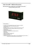
MULTIDROP CONTROL PANEL V1.8 SOFTWARE USER MANUAL MULTIDROP CONTROL PANEL V1.8 SOFTWARE USER MANUAL This handbook is provided in confidence, as a technical reference for use solely by the purchaser of the equipment. The handbook or its contents may not be reproduced or distributed without written consent from Tomco Electronics Pty Ltd. Tomco Electronics Pty Ltd 17 Clarke St., Norwood, South Australia 5067 AUSTRALIA Ph +61 8 83642203 Fax +61 8 83642202 Tomco Electronics Pty Ltd November 2002 CONTENTS SECTION TITLE A Special notes for a linear amplifier configuration. 1 Transmitter Interface Introduction 2 Transmitter Control Panel 3 Receiver Control Panel 4 Predistortion Panel (factory only) 5 Pulse Shape Setup Panel 6 Direct Digital Synthesiser Panel 7 Multidrop Command Panel (factory only) 8 Module Information Panel 9 Main Menu Operations 10 Calibration Factors 11 Hardware Setup Notes Section A: Special Notes for a Linear Amplifier Configuration The transmitter control card that is the focus of much of this document was originally designed for use in Tomco’s pulse generating transmitters. In this configuration, the control card is used to provide all amplitude modulation to the power amplifier. A great deal of the functionality of the control card and this interface software is devoted to the generation of modulation pulses. A slightly modified version of the transmitter control card is used in our linear range of amplifiers in order to provide status monitoring and protection functions. The pulse generation functions do not affect the output in this configuration and should be ignored in the rest of this document. T000830f.doc Page 1 Section 1: Transmitter Interface Introduction The transmitter contains a transmitter control module that is responsible for the following functions: • generating a transmitter RF amplitude modulation signal • generating an RF phase inversion signal • generating a transmit RF gating signal (and an optional receiver gating signal) • providing protection against excessive load mismatch • providing protection against excessive duty cycle and or pulse width • monitoring the RF line voltage at a pre-specified point within a pulse • monitoring the peak RF forward and reflected voltages • monitoring the internal transmitter air temperature The transmitter control module has a serial interface to communicate with a PC running the Windows based Multidrop Control Panel software or similar. The serial interface can take the form of either RS232 or RS485 as selected by a switch on the rear of the transmitter. Only RS485 is capable of being used in a networked or multidrop mode (with more than one device on the bus). RS485 also offers more immunity to the strong RF interference generated by the transmitter. The transmitter is able to store up to 8 pulse descriptions in volatile RAM at any one time. Each of these pulse descriptions refers to one of the standard or user specified pulse shape templates. The pulse shape templates are stored in non-volatile FLASH memory. There are 6 standard pulse shape templates and up to 4 user specified templates. Each pulse description consists of a reference to one of the pulse shape templates, a 3dB pulse width, an amplitude, a pulse code word and pre and post gate delay settings. All timing is specified in increments of 0.1uS. Changing between one of the 8 pulse descriptions is normally achieved by modifying the digital 3-bit word applied to the transmitter control bus. In this way pulses can be selected on a pulse to pulse basis within a pulse train. Note that the software is also capable of taking control of the pulse select address lines to provide a more convenient means for the user to select between pulse descriptions. The transmitter control module is able to remember its configuration with no power applied. This means that PC software control of the transmitter is not necessary to produce transmit pulses. In many cases, once the transmitter control module has been set up to the user’s requirements, it will not need to be set up again. T000830f.doc Page 2 Section 2: Transmitter Control Panel Figure 1 Control Panel for Transmitter Figure 1 shows a screen capture of the main transmitter control panel. This is where the 8 possible pulse descriptions are set up, and where transmitter status is displayed. The top section of the window provides a means of changing the Pulse Select Source. If the source is set to external, then the pulse number is selected via the external control bus. If the source is set to internal then the pulse is selected via the up&down spin buttons and in the Pulse Number box. Note that in either case, the Selected Pulse Number will be displayed in the Transmitter Status section of the window. Also included in the top section of the window, Transmitter Select, provides a means of selecting the specific transmitter being addressed in a multi-transmitter system. The pulse description table, appearing mid-window, is where each of the 8 possible pulse descriptions is set up. Each pulse description consists of: • The pulse shape template number to be used. (Gaussian, Square etc.) • The pulse length in uS (0.1uS steps). The pulse length is measured between the half power (-3dB) points on the pulse. • The pulse amplitude expressed as a percentage of maximum. • The pulse code to be used expressed as a string of 0s and 1s. If no pulse encoding is required, then a single 1 should be used. T000830f.doc Page 3 • The pre-tx-gate and post-tx-gate times specify the transmitter “gate overlap” to be used. (Tx_gate will be applied for pre-tx-gate uS before modulation begins and will be applied for post-tx-gate uS after the end of modulation.) Tomco normally suggests using a value of 1uS for these times. • The pre-rx-gate and post-rx-gate times have a similar function, except this time applying to the rx_gate signal. • The interbit delay aids in creating clean transitions of multibit pulse codes (particularly those with short bit times). It causes the modulation signal to be set to zero for the specified interbit delay at the end of each bit. The starting points of each bit remain fixed in time as the interbit delay is varied. The transmitter may already be set up with a set of such pulse descriptions. They can be read be pressing the TX_Read button while the transmitter is on. In order to store a new set of pulse descriptions, the TX_Update button should be pressed. Note that this button is also used to update the Vreflected trip threshold level , the Use Predistortion flag and the Pulse Select Source in non-volatile memory. The Vreflected trip threshold is used to set a threshold for the mismatch protection circuitry. This has been factory preset to a safe level and should not be modified. The Use Predistortion flag selects whether or not the transmitter control module applies “predistortion” to the modulation shape. Predistortion is used to linearise the modulation input/ rf output characteristic and is factory preset. It can not be turned off by the user. The transmitter status consists of the various pieces of information that the transmitter reports back to the PC and is updated approximately every second. • The Enabled flag indicates whether or not the transmitter is currently enabled. • The Selected Pulse Number indicates the pulse number that the transmitter is currently using. • The Line Voltage is sampled at a pre-specified point (usually the peak) on the pulse. The magnitude is expressed as a number from 0 to 99. This is not a calibrated measurement, and is intended for relative measurements only. This reading is rarely implemented on Tomco transmitters. • The Forward Voltage is a measure of the peak forward voltage detected at the transmitter output. It will be maximised when the load is properly matched. • The Reflected Voltage is a measure of the peak reflected voltage detected at the transmitter output. It will be minimised when the load is properly matched. Note that this reading can be used as a rough means of tuning the load (antenna). Also note that If the load is so poorly matched that it causes the transmitter to shut down, then the pulse amplitude can be turned down in order to enable tuning of the load. • The VSWR (Voltage Standing Wave Ratio) is a value calculated from the forward and reflected voltage and is a good measure of the mismatch presented by the load to the transmitter. • The Internal Temperature is measured by a sensor mounted within the transmitter air stream. • The Temperature OK flag indicates whether the transmitter has shut down due to any of the modules over-heating. T000830f.doc Page 4 • The Power Supply OK flag indicates whether the main DC supply rail is OK. • The Duty Limit Exceeded flag indicates if the allowed maximum transmitter duty cycle has been exceeded at some point after the flag was last reset. This flag is latched by the software and can be cleared by Clear Latched Flags button. Note that this flag is often set on power-up, and can be safely cleared. • The Double Trigger Detected flag indicates if a positive trigger signal edge was received while a transmit pulse was in progress. Such a trigger signal is otherwise ignored by the transmitter and poses no problems, so this flag is intended for diagnostic purposes only. It can be cleared by Clear Latched Flags. • The Mismatch Detected flag indicates that an RF output mismatch condition was detected. It can be cleared by Clear Latched Flags. T000830f.doc Page 5 Section 3: Receiver Control Panel Figure 2 Receiver Control Panel The receiver control panel allows the receiver gains and base-band filter responses to be set up and read. Two modes of editing the gains of each receiver are possible. The first mode allows each of the receiver gains to be modified together by modifying the Gain in the box labelled All. The second mode allows each receiver gain to be modified separately. The baseband filter selection is common to all receivers, and is selected by one of the four available radio buttons. In order for the hardware to reflect the changes, the Update All button should be pressed. To read the currently values used by the hardware, the Read All button should be pressed. Note that unlike the other modules, the receiver gain control module is not able to store the values in non-volatile memory, and must be re-entered after each power up. T000830f.doc Page 6 Section 4: Predistortion Panel (factory only) Figure 3 Predistortion Setup Panel The predistortion panel is intended for factory use only. It is where the predistortion table is setup in order to linearise a particular transmitter. The predistortion curve is modified by drawing a series of straight line segments. A line segment is drawn by pressing and holding the left mouse button at the start of the line, and releasing the button at the desired end point of the line. Note that normally the right half of the predistortion curve should mirror the left half. This is easily achieved by pressing the Mirror L->R. A previously stored predistortion curve can be loaded by pressing the Read button. The Update button is used to write a new predistortion curve to the transmitters nonvolatile memory. Note that the modifications will not be seen until the pulse descriptions are reloaded in the control window. T000830f.doc Page 7 Section 5: Pulse Shape Setup Panel Figure 4 Pulse Shape Setup Panel The Pulse Shape Setup Panel is used to view each of the factory defined and user defined pulse shape templates. It also enables user defined pulse templates to be written to the transmitter. In addition it allows the RF line voltage sample point to be defined for each template. (See Section 2 for a description of the RF line voltage). The green line is a graphical indication of this point. The two red lines are spaced at exactly 200 samples and are intended to show the portion of the shape that is considered to be the 3dB pulse width. Note that the lines are always centred on the centre of the display window and so will only be in the correct location for a symmetrical shape. In order to generate a user defined shape, a program such as Microsoft Excel should be used to produce a single column of values ranging from –1.0 to +1.0 to represent the pulse shape points in time. A magnitude of 1.0 corresponds to maximum amplitude and a negative value indicates a phase flip of the RF waveform of 180 degrees. In order for the pulse width to be correct, the half power points of the shape should be spaced by 200 samples. The total shape length should be no more than 5000 samples long. In order to store a user shape, the desired User tab button should be pressed; the column of values should be “copied” in Excel, and then the Paste Pulse Shape button pressed. The pulse shape should appear in the window along with the two red lines indicating –3dB pulse width. In order to then store all of the shapes in the transmitter, the Update TX Shapes button should be pressed. Pulse descriptions must be reloaded via the main control window in order for the changes to be reflected at the transmitter output. T000830f.doc Page 8 Section 6: Direct Digital Synthesiser Panel Figure 5 Direct Digital Synthesiser Panel This panel is where all configuration for the Direct Digital Synthesiser (DDS) is carried out. The DDS is able to be used in a frequency agile mode such as FDI where the frequency can change from pulse to pulse in a pulse sequence. In order to achieve this, the unit stores up to 16 phase/frequency slots. A particular slot is selected via the digital control bus on the back of the DDS unit. This mode of operation requires sophisticated timing and need not be considered if a single frequency of operation is needed. The Phase/Freq Slot To Edit up/down buttons allows editing of each of the 16 possible slots. For single frequency operation, slot 0 is all that need be changed. Also, to ensure that slot 0 is used by the DDS regardless of the control bus address, the Use Phase/Freq Slot 0 Only box should be checked. The DDS Reference Frequency box shows the frequency in MHz of the clock used to drive the Direct Digital Synthesis ICs. This is fixed for a particular unit. The actual reference frequency may be slightly offset from this Each synthesiser channel is able to produce a frequency governed by a 32-bit frequency select number. This number is added to a 32 bit phase accumulator word on each DDS clock cycle to address a sine lookup table. The DDS frequency output is thus proportional to the frequency select number and is calculated as: DDS Ref. Frequency x Frequency Select Word T000830f.doc Page 9 232 This calculation is performed by the user interface software, so the user need not worry about those details. The software will find the frequency select word that is closest to the chosen frequency. Note that the frequency resolution is 0.042 hertz for a 180MHz reference clock. The user must be careful to ensure that coherence is maintained after the rounding has been performed. Also, the starting phase of each channel may be specified in steps of 11.25 degrees. Typically this feature is used to specify a 90 degree offset between I and Q local oscillator channels. The Update All button must be used to send these settings for every used slot to the DDS unit. The settings stored in the DDS unit can be retrieved by pressing the Load From DDS button. The DDS unit has four separate output channels (TX, QP LO, IP LO, 1st LO) that will all be in phase when the frequency and phase settings for each are identical. The TX channel is split into 8 separate drive outputs available at the rear of the unit. The TX channel is also used to drive a test and accessory output, but can only be used in a mutually exclusive manner. This is selected by the Output Select radio buttons. The TX outputs are switched on and off by the TTL level TX_GATE input at the rear of the DDS unit. All of the LO outputs can be switched on and off in one of two ways (typically used for receiver blanking). The first option is by using the inverse of the TX_GATE such that the LO outputs are on when the TX drive is off and vice versa. The second option is to use the separate RX_GATE input so that more sophisticated timing may be used for receiver blanking. The LO Blanking Input radio buttons are used to do this selection. The software user is able enable and disable the transmitter output via the TX Drive On check box. In order to avoid having to re-enter DDS control information after a power cycle, an onboard non-volatile memory can store this information. By pressing Write Default Settings, the non-volatile memory will be loaded with the currently active DDS settings. These settings will then be automatically restored on each power-up. This feature means that for normal operation, software re-configuration is not necessary. T000830f.doc Page 10 Section 7: Multidrop Command Panel Figure 6 Multidrop Command Panel The multidrop command panel is used for low level testing of multidrop commands. It uses a primitive interface to set up command packets and receive response packets. Note that when constructing the data bytes for a transmit packet (done in the large grid), the software counts the number of filled in transmit byte boxes, and uses this to fill in the Data # box. T000830f.doc Page 11 Section 8: Module Information Panel Figure 7 Module Information Panel The module information panel is used to provide an easy means of detecting the various modules that are functioning and connected to the RS485 multidrop bus. By pressing the Find Modules button, the software will scan through the available multidrop addresses and display information about any modules it finds. Information about the multidrop address, module class, module type, firmware version and serial number are displayed. T000830f.doc Page 12 Section 9: Main Menu Operations The File menu has options to save and open configuration files. These files provide a means of storing all of the configuration information contained on the various control panels for later retrieval. The Setup menu allows a particular PC serial (COM) port to be chosen for multidrop communication. The COM port to use will depend on the way the PC has been set up. This setting is remembered next time the program is run. T000830f.doc Page 13 Section 10: Calibration Factors Some calibration factors are stored under the MS-Windows Registry and can be modified using the program "regedit" to be found in the Windows main directory. Default values for these parameters are created when MCP is first run on a particular computer. These factors are located in the registry under: HKEY_LOCAL_MACHINE\SOFTWARE\Tomco\MCP ComPort Can be modified using the MCP software, and need not be altered by regedit. Stores the serial port to be used by MCP. ShapeClockFreq Should be set to the frequency (in MHz) of the reference clock. This will scale the pulse widths generated by the control card. Typically 16.0 VfwdCalFactor The forward voltage displayed in the status window is multiplied by this number before being displayed. VrefCalFactor The reflected voltage displayed in the status window is multiplied by this number before being displayed. VsampCalFactor The line sample voltage displayed in the status window is multipled by this number before being displayed. T000830f.doc Page 14 Section 11: Hardware Setup Notes This section relates to setup of the hardware relating to multi-drop communications. Each of the multidrop devices contains a switch or jumper to allow selection between RS232 or RS485 communication. RS232 communication is convenient to use when only one device needs to be connected at a time. It is not possible to have multiple RS232 devices connected on a single bus. Also, the RS232 bus is not particularly immune to the relatively strong RF fields produced by the transmitter and so is not suitable for use in an operational environment. However, an RS232 interface is standard with all PCs and so provides a convenient means of testing. RS485 communication is very similar to RS232; bytes are sent with the same bit format and baud rate. The difference is that all communication takes place on a bus consisting of a single differential pair of wires. The bus and protocol have been devised such that many devices can be connected to it. The screened differential bus also provides a high degree of immunity from interfering signals. In order for a standard PC to use RS485 communications it must be set up with either a special RS485 capable expansion card or an RS232 to RS485 converter. The expansion card has the advantage that it does not require external power to operate. In order to use a card such as the Advantek PCL740, it must be plugged into a spare ISA slot in the PC. Also, the card must be configured (via jumpers) to use a unique Interrupt Request number (IRQ) and IO base address. The card’s manual should be consulted to see how to do this. It is often safest to use the IO address and IRQ assigned to COM1 or COM2 and then to disable that COM port in the computers BIOS setup. T000830f.doc Page 15