1
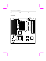
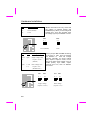
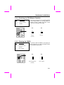
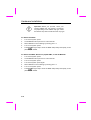
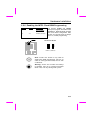
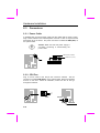
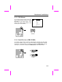
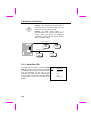
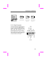
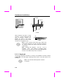
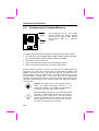
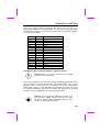
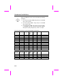
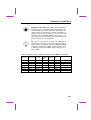
Chapter 2
Hardware Installation
This chapter gives you a step-by-step procedure on how to install your system.
Follow each section accordingly.
Caution: Electrostatic discharge (ESD) can
damage your processor, disk drives,
expansion boards, and other components.
Always observe the following precautions
before you install a system component.
1.
Do not remove a component from its
protective packaging until you are ready
to install it.
2.
Wear a wrist ground strap and attach it
to a metal part of the system unit before
handling a component. If a wrist strap is
not available, maintain contact with the
system unit throughout any procedure
requiring ESD protection.
2-1
Hardware Installation
2.1
Jumper and Connector Locations
The following figure shows the locations of the jumpers and connectors on the
system board:
PS2 MS
KBC
KB
USB
PWR
COM2
I
S
A
3
I
S
A
2
I
S
A
1
COM1
BIOS
JP1301 & JP1302
PCI
4
PCI
3
PCI
2
PCI
1
S
I
M
M
4
PRINTER
FDC
RTC
JP5
IDE2
JP1
FAN
JP8
JP4
JP12
IrDA
JP10
JP3
JP13
JP11
HDD LED
PANEL
2-2
IDE1
S
I
M
M
3
S
I
M
M
2
S
I
M
M
1
Hardware Installation
Jumpers:
JP11:
JP12:
JP3,JP13:
JP10:
JP1:
JP4:
JP5:
JP8:
JP1301,1302:
CPU core voltage setting Vcore)
(
I/O voltage setting V
( io)
CPU type (Single/Dual voltage,Vcpuio selection.)
CPU frequency ratio
CPU external (bus) clock
Onboard PS/2 mouse enable/disable
Clear CMOS
Onboard Super I/O enable/disable
INTEL Flash ROM programming enable/disable
Connectors:
KB (CN2):
PWR (CN3):
PS2 MS (CN4):
USB (CN5):
COM1 (CN7):
COM2 (CN6):
FDC (CN8):
PRINTER (CN9):
IDE1 (CN10):
IDE2 (CN11):
FAN (CN15):
IrDA (CN14):
HDD LED (CN12):
PANEL (CN16):
AT keyboard connector
AT power connector
PS/2 mouse connector
USB connector
COM1 connector
COM2 connector
Floppy drive connector
Printer connector
IDE1 primary channel
IDE2 secondary channel
CPU fan connector
IrDA connector
HDD LED connector
Front panel (Multifunction) connector
2-3
Hardware Installation
2.2
Jumpers
Jumpers are made by pin headers and plastic connecting caps for the purpose
of customizing your hardware. Doing so requires basic knowledge of computer
hardware, be sure you understand the meaning of the jumpers before you
change any setting. The onboard jumpers are normally set to their default with
optimized settings.
On the mainboard, normally there is a bold line marked beside pin 1 of the
jumper, sometimes, there are numbers also. If we connect (short) plastic cap to
pin 1 and 2, we will say set it at 1-2, and when we say jumper is open, that
means no plastic cap connected to jumper pins.
2-4
1
2
1
2
Open
Short
1
2
3
Jumper set at 12
1
2
3
Jumper set at 2-3
Hardware Installation
2.2.1 Setting the CPU Voltage
JP11
1-2
3-4
5-6
7-8
9-10
11-12
CPU Core Voltage (Vcore)
3.45V (default for P54C)
3.52V (Cyrix or AMD K5)
2.5V
3.2V (AMD K6-233)
2.8V (PP/MT P55C)
2.9V (AMD K6-166/200)
JP11
JP11 is used to select CPU core
voltage (Vcore), normally it is set to
default 3.45V for INTEL Pentium P54C.
It must be changed if you have CPU
with different core voltage, such as
INTEL PP/MT (P55C), AMD K5/K6 and
Cyrix 6x86, refer to the CPU
specification for more details.
JP11
JP11
11 9 7 5 3 1
11 9 7 5 3 1
11 9 7 5 3 1
12 10 8 6 4 2
12 10 8 6 4 2
12 10 8 6 4 2
3.2V
3.52V
3.43V
( AMD K6-233)
( Cyrix 6x86 or
AMD K5)
(default for
P54C)
JP11
11 9 7 5 3 1
JP11
11 9 7 5 3 1
12 10 8 6 4 2
2.9V
( AMD K6166/200)
12 10 8 6 4 2
2.8V
( PP/MT P55C)
Warning: The heat dissipation of Intel PP/MT-233Hz, AMD
K6-200/233MHz exceed the original design of this mainboard.
Please make sure that you have installed CPU fan properly if
Intel PP/MT-233 or AMD K6-200/233 is being selected to use.
It may cause your system unstable if you can not meet the
heat dissipation requirement from above CPU type. It is
recommended to adopt larger fan on these CPU for better air
flow in the system.
2-5
Hardware Installation
JP12
I/O Voltage (Vio)
1-2
3-4
3.43V (default)
3.52V
JP12 is reserved for test only, which sets
the voltage of onboard chipset and
PBSRAM (Vio). When you are using dual
voltage CPU, JP12 also provides CPU
I/O voltage (Vcpuio).The default is 3.43V.
JP12
JP12
3 1
3 1
4 2
4 2
3.43V (default)
3.52V
JP3
JP13
CPU Type (Vcpuio)
1-2 &
3-4
Open
Single voltage CPU
Vcpuio = Vcore
(default)
Open
1-2 &
3-4
Dual voltage CPU
Vcpuio = Vio
(PP/MT P55C)
Set the jumper JP3 and JP13 according
to the type of CPU. They are actually
the selection of
CPU I/O Voltage
(Vcpuio). Normally, for single voltage
CPU, Vcpuio is equal to Vcore, but for
CPU that needs dual voltage such as
PP/MT (P55C), Cyrix 6x86L, Vcpuio
must be set to Vio, and it is different
from Vcore.
JP3
JP13
JP3
JP13
3 1
3 1
3 1
3 1
4 2
4 2
4 2
4 2
Single voltage
(Vcpuio = Vcore)
2-6
Dual voltage
(Vcpuio = Vio)
Hardware Installation
CPU Type
INTEL P54C
INTEL PP/MT
AMD K5
AMD K6-166/200
AMD K6-233
Cyrix 6x86
Cyrix 6x86L
Vcore
3.43V
2.8V
3.52V
2.9V
3.2V
3.52V
2.8V
Vio
3.43V
3.43V
3.43V
3.43V
3.43V
3.43V
3.43V
Vcpuio
Vcore
Vio
Vcore
Vio
Vio
Vcore
Vio
JP11
1-2
9-10
3-4
11-12
7-8
3-4
9-10
JP12
1-2
1-2
1-2
1-2
1-2
1-2
1-2
JP3
1-2 & 3-4
Open
1-2 & 3-4
Open
Open
1-2 & 3-4
Open
JP13
Open
1-2 & 3-4
Open
1-2 & 3-4
1-2 & 3-4
Open
1-2 & 3-4
Caution: Above table is possible settings of current
CPU available on the market. The correct setting may
vary because of new CPU product, refer to your CPU
specification for more details.
2.2.2 Selecting the CPU Frequency
JP10
CPU Frequency Ratio
1-2 & 3-4
3-4 & 5-6
5-6 & 7-8
1-2 & 7-8
1.5x (3.5x)
2x
2.5x (1.75x)
3x
Intel Pentium, Cyrix 6x86 and
AMD K5/K6 CPU are designed to
have different Internal (Core) and
External (Bus) frequency. The
ratio of Core/Bus frequency is
selected by JP10, which CPU is
using to multiply external clock
and produce internal frequency.
2-7
Hardware Installation
Core frequency = Ratio * External bus clock
JP10
JP10
JP10
JP10
7 5 3 1
7 5 3 1
7 5 3 1
7 5 3 1
8 6 4 2
8 6 4 2
8 6 4 2
8 6 4 2
2x
2.5x
(1.75x)
3x
1.5x
(3.5x)
Tip: Intel PP/MT 233MHz is using 1.5x jumper setting for 3.5x
frequency ratio, and AMD PR166 is using 2.5x setting for
1.75x frequency ratio..
JP1
1-2 & 3-4
Open
1-2
3-4
CPU External Clock
50MHz
55MHz
60MHz
66MHz
JP1 is the selections of CPU external
clock (bus clock), which is actually the
clock from clock generator.
JP1
JP1
JP1
JP1
3 1
3 1
3 1
3 1
4 2
4 2
4 2
4 2
50MHz
55MHz
60MHz
66MHz
Caution: Following table are possible settings of
current CPU available on the market. The correct
setting may vary because of new CPU product,
refer to your CPU specification for more details.
2-8
Hardware Installation
Intel Pentium
P54C 75
P54C 90
P54C 100
P54C 120
P54C 133
P54C 150
P54C 166
P54C 200
Intel Pentium
PP/MT 150
PP/MT 166
PP/MT 200
PP/MT 233
Cyrix 6x86
P120+
P133+
P150+
P166+
AMD K5
PR75
PR90
PR100
PR120
PR133
PR166
AMD K6
PR2-166
PR2-200
PR2-233
CPU Core
Frequency
75MHz =
90MHz =
100MHz =
120MHz =
133MHz =
150MHz =
166MHz =
200MHz =
Ratio
CPU Core
Frequency
150MHz =
166MHz =
200MHz =
233MHz =
Ratio
CPU Core
Frequency
100MHz =
110MHz =
120MHz =
133MHz =
Ratio
CPU Core
Frequency
75MHz =
90MHz =
100MHz =
90MHz =
100MHz =
116MHz =
Ratio
CPU Core
Frequency
166MHz =
200MHz =
233MHz =
Ratio
1.5x
1.5x
1.5x
2x
2x
2.5x
2.5x
3x
2.5x
2.5x
3x
3.5x
2x
2x
2x
2x
1.5x
1.5x
1.5x
1.5x
1.5x
1.75x
2.5x
3x
3.5x
External Bus
Clock
50MHz
60MHz
66MHz
60MHz
66MHz
60MHz
66MHz
66MHz
JP10
JP1
1-2 & 3-4
1-2 & 3-4
1-2 & 3-4
3-4 & 5-6
3-4 & 5-6
5-6 & 7-8
5-6 & 7-8
1-2 & 7-8
1-2 & 3-4
1-2
3-4
1-2
3-4
1-2
3-4
3-4
External Bus
Clock
60MHz
66MHz
66MHz
66MHz
JP10
JP1
5-6 & 7-8
5-6 & 7-8
1-2 & 7-8
1-2 & 3-4
1-2
3-4
3-4
3-4
External Bus
Clock
50MHz
55MHz
60MHz
66MHz
JP10
JP1
3-4 & 5-6
3-4 & 5-6
3-4 & 5-6
3-4 & 5-6
1-2 & 3-4
Open
1-2
3-4
External Bus
Clock
50MHz
60MHz
66MHz
60MHz
66MHz
66MHz
JP10
JP1
1-2 & 3-4
1-2 & 3-4
1-2 & 3-4
1-2 & 3-4
1-2 & 3-4
5-6 & 7-8
1-2 & 3-4
1-2
3-4
1-2
3-4
3-4
External Bus
Clock
66MHz
66MHz
66MHz
JP10
JP1
5-6 & 7-8
1-2 & 7-8
1-2 & 3-4
3-4
3-4
3-4
2-9
Hardware Installation
Note: Cyrix 6x86 and AMD K5 CPU use P-rating
for the reference of CPU benchmark compared
with INTEL P54C, their internal core frequency is
not exactly equal to P-rating marked on the CPU.
For example, Cyrix P166+ is 133MHz but
performance is almost equal to P54C 166MHz
and AMD PR133 is 100MHz but performance is
almost equal to INTEL P54C 133MHz.
2.2.3 Disabling the Onboard Super I/O Controller
JP8
Onboard Super I/O
1-2
2-3
Enable (default)
Disable
The board is default to enable the onboard
Super I/O controller. In case you wish to use
an external I/O control card, you need to
disable the onboard I/O before using the
external I/O card. To disable it, set the jumper
JP8 to 2-3.
JP8
JP8
3 2 1
3 2 1
Enable
(default)
2-10
Disable
Hardware Installation
2.2.4 Disabling the PS/2 Mouse Function
JP4
PS/2 Mouse
Short
Open
Enable (default)
Disable
The PS/2 mouse function is normally enabled
and occupies IRQ12. To reassign IRQ12 to
another function, disable the PS/2 mouse
function by opening jumper JP4.
JP4
JP4
2 1
2 1
Enable
Disable
(default)
2.2.5 Clearing the CMOS
JP5
Clear CMOS
1-2
Normal operation
(default)
Clear CMOS
2-3
You need to clear the CMOS if you forget your
system password. To clear the CMOS, follow
the procedures listed below:
JP5
1
2
3
Normal Operation
(default)
JP5
1
2
3
Clear CMOS
2-11
Hardware Installation
Important: Before you proceed, check your
onboard CMOS chip. The clearing procedures
vary depending on the CMOS chip type. Read
the CMOS chip label to determine the chip type.
For Dallas DS12887A:
1.
Turn off the system power.
2.
Locate JP5 and short pins 2-3 for a few seconds.
3.
Return JP5 to its normal setting by shorting pins 1-2.
4.
Turn on the system power.
5.
Press
during bootup to enter the BIOS Setup Utility and specify a new
password, if needed.
For Dallas DS12B887, Benchmarq bq3287AMT, or SGS ST M48T86:
1.
Turn off the system power.
2.
Locate JP5 and short pins 2-3 for a few seconds.
3.
Turn on the system power.
4.
Turn off the system power again.
5.
Return JP5 to its normal setting by shorting pins 1-2.
6.
Turn on the system power.
7.
Press
during bootup to enter the BIOS Setup Utility and specify a new
password, if needed.
2-12
Hardware Installation
2.2.6 Enabling the INTEL Flash ROM Programming
JP1301
JP1302
Flash ROM
Programming
2-3
2-3
Enable (default)
The jumpers JP1301 and JP1302
allow you to program the INTEL Flash
ROM BIOS. Because BIOS will write
back PnP ESCD configuration data,
JP1301 and JP1302 must be always
set to 2-3, enable programming.
JP1301 and JP1302
1
2
3
1
2
3
Enable (default)
Note: JP1301 and JP1302 is only used for
INTEL flash ROM programming, they are no
effect for other type Flash ROM, such as SST
or Winbond.
Warning: JP1301 and JP1302 must always
be enabled, fail to do so causing inconsistent
BIOS code, and may damage the system.
2-13
Hardware Installation
2.3
Connectors
2.3.1 Power Cable
A standard baby AT (PS/2) power supply has two cables with six wires on each.
Plug in these cables to the onboard power connector in such a way that all the
black wires are in the center. The power connector is marked as PWR (CN3) on
the system board.
Caution: Make sure that the power supply is
off before connecting or disconnecting the
power cable.
Black wire (GND)
Red wire (+5V)
PWR
2.3.2 CPU Fan
Plug in the fan cable to the two-pin fan connector onboard. The fan
connector is marked FAN (CN15) on the system board. Attach the heatsink
and fan to the CPU. Check its orientation, make sure the air flow go
through the heatsink.
+12V
GND
FAN
Air Flow
Heatsink
2-14
Hardware Installation
2.3.3 PS/2 Mouse
Pin
1
2
3
4
5
6
To connect a PS/2 mouse, insert the
PS/2 mouse bracket connector to PS2
MS (CN4) on the system board. Then
plug in the PS/2 mouse cable to the
mouse port on the bracket.
Description
MS DATA
NC
GND
+5V
MS CLK
NC
3 1 2 4
5
6
PS2 MS
2.3.4 Serial Devices (COM1/COM2)
To support serial devices, insert the serial device connector into the serial
port on the bracket. Plug in the 10-pin flat cable to the appropriate onboard
connectors. The serial port 1 connector is marked as COM1 (CN7) and the
serial port 2 connector is marked as COM2 (CN6) on the system board.
1
2
9
10
COM2
1
2
9
10
COM1
2-15
Hardware Installation
2.3.5 USB Device (optional)
Pin
1
3
5
7
9
You need a USB bracket to
have your system to support
additional USB device(s). To
attach a USB bracket, simply
insert the bracket cable to the
onboard USB connector marked
as USB (CN5).
Description
V0
D0D0+
GND
NC
Pin
2
4
6
8
10
Description
V1
D1D1+
GND
NC
1
6
5
10
USB
2.3.6 Floppy Drive
Connect the 34-pin floppy drive cable to the floppy drive connector marked as
FDC (CN8) on the system board.
1
33
2
34
FDC
2-16
Hardware Installation
2.3.7 Printer
Plug in the 26-pin printer flat cable to the onboard parallel connector
marked as PRINTER (CN9) on the board.
1
2
25
26
PRINTER
2.3.8
IDE Hard Disk and CD ROM
This mainboard supports two 40 pin IDE connectors marked as IDE1
(CN10) and IDE2 (CN11). IDE1 is also known as primary channel and
IDE2 as secondary channel, each channel supports two IDE devices that
makes total of four devices.
In order to work together, the two devices on each channel must be set
differently to master and slave mode, either one can be hard disk or
CDROM. The setting as master or slave mode depends on the jumper
on your IDE device, please refer to your hard disk and CDROM manual
accordingly.
Connect your first IDE hard disk to master mode of the primary channel.
If you have second IDE device to install in your system, connect it as
slave mode on the same channel, and the third and fourth device can be
connected on secondary channel as master and slave mode respectively.
1
39
2
40
IDE2
1
39
2
40
IDE1
2-17
Hardware Installation
Caution: The specification of IDE cable is
maximum 46cm (18 inches), make sure your
cable does not excess this length.
Caution: For better signal quality, it is
recommended to set far end side device to
master mode and follow the suggested
sequence to install your new device . Please
refer to following figure.
Primary Channel
Slave
(2nd)
Master
(1st)
Secondary Channel
Slave
(4th)
Master
(3rd)
2.3.9 Hard Disk LED
The HDD LED connector is marked as HDD
LED on the board. This connector is designed
for different type of housing, actually only two
pins are necessary for the LED. If your
housing has four pin connector, simply plug it
in. If you have only two pin connector, please
connect to pin 1-2 or pin 3-4 according to the
polarity.
2-18
Pin
Description
1
2
3
4
HDD LED
GND
GND
HDD LED
Hardware Installation
4 3 2 1
4 3 2 1
4 3 2 1
+ - - +
+ - - +
+ - - +
HDD LED
HDD LED
HDD LED
4-pin connector
2-pin connector
at pin 1-2
2-pin connector
at pin 3-4
2.3.10 Panel Connector
The Panel (multifunction) connector is a 20pin connector marked as PANEL (CN16) on
the board. Attach the power LED, keylock,
speaker, reset switch, suspend switch, and
green mode LED connectors to the
corresponding pins as shown in the figure.
Some housings have a five-pin connector
for the keylock and power LED Since power
LED and keylock are aligned together, you
can still use this kind of connector.
S
U
S
P
E
N
D
G
R
E
E
N
S
U
S
P
E
N
D
R
E
G
G
S G
+ G L
5 N EN S S NN E N
V D DD W W DC T D
11
1
20
10
G KG R
N EN E
D YD S
L
E
O
T
C
K
P
O
W
E
R
S + G N S
P 5 N C P
E V D
E
A
A
K
K
E
E
LR
R
E
D
PANEL
2-19
Hardware Installation
Green LED
Suspend SW
Reset
+
+
+
11
1
20
10
+
+
+
Speaker
Power LED
Keylock
PANEL
Other housings may have a 12-pin
connector. If your housing has this
type of connector, connect it to
PANEL as shown in the figure.
Make sure that the red wire of the
connector is connected to +5V.
+5V
11
1
20
10
PANEL
Note: If your housing comes with Turbo switch and
Turbo LED connectors, you may use these connectors
for Suspend switch and Green mode LED functions,
respectively.
Note: Pressing the Suspend switch allows you to
manually
force
the system to suspend mode.
However, this is possible only if the Power Management
function in the BIOS Setup menu is enabled.
2.3.11 Keyboard
The onboard keyboard connector is a five-pin AT-compatible connector marked
as KB (CN2) . The view angle of drawing shown here is from back panel of the
housing.
Note: The mini DIN PS/2 keyboard connector
is optional.
2-20
Hardware Installation
PCB
AT KB
2.3.12 IrDA Connector
Serial port 2 can be configured to support wireless infrared module, with
this module and application software such as Laplink, user can transfer
files to or from laptops, notebooks, PDA and printers. This mainboard
supports IrDA (115Kbps, 1 meter) as well as ASK-IR (19.2Kbps).
Install infrared module onto IrDA (CN14)
connector and enable infrared function
from BIOS setup, make sure to have
correct orientation when you plug onto
IrDA connector.
Pin
Description
1
2
3
4
5
6
+5V
IRRX
GND
IRTX
NC
+3.3V
Note: Onboard serial port 2 (COM2) will not be
available afterIrDA connector is enabled.
654321
IrDA
2-21
Hardware Installation
2.4
Configuring the System Memory
Pin 1 of
Bank1
Pin 1 of
Bank0
This mainboard has four 72 pin SIMM
sockets (Single-in-line Memory Module)
that allow you to install system memory
from minimum 8MB up to maximum
512MB.
The SIMM supported by this mainboard can be identified by 4 kinds of factors:
♦ Size: single side, 1Mx32 (4MB), 4Mx32 (16MB), 16Mx32 (64MB), and double
side, 1Mx32x2 (8MB), 4Mx32x2 (32MB), 16Mx32x2 (128MB).
♦ Speed: 60ns or 70ns access time
♦ Type: FPM (Fast page mode) or EDO (Extended data output)
♦ Parity: without parity (32 bit wide) or with parity (36 bit wide).
Because Pentium processor has 64 bit bus width, the four SIMM sockets are
arranged in two banks of two sockets each, they are Bank0 and Bank1. Both
SIMMs in each bank must be in the same size and type. It is allowed to have
different speed and type in different bank, for example, 70ns FPM in one bank
and 60ns EDO in another bank, in such case, each bank is independently
optimized for maximum performance. The memory timing requires at least 70ns
fast page mode DRAM chip, but for optimum performance, 60ns EDO DRAM is
recommended.
Warning: The default memory timing setting is 60ns to
obtain the optimal performance. Because of the
specification limitation, 70ns SIMM is recommended to
be used only for CPU external clock 60MHz.
Tip: EDO DRAM is designed to improve the DRAM read
performance. Unlike traditional fast page mode, that tristates the memory output data to start the precharge
activity, EDO DRAM holds the memory data valid until
the next memory access cycle, which is similar to pipeline effect and reduces one clock state.
2-22
Hardware Installation
There is no jumper setting required for the memory size or type. It is
automatically detected by the system BIOS. You can use any single side SIMM
combination list below for, and the total memory size is to add them together,
the maximum is 512MB.
SIMM1
None
4MB
8MB
16MB
32MB
64MB
128MB
SIMM2
None
4MB
8MB
16MB
32MB
64MB
128MB
Subtotal of Bank0
0MB
8MB
16MB
32MB
64MB
128MB
256MB
SIMM3
None
4MB
8MB
16MB
32MB
64MB
128MB
SIMM4
None
4MB
8MB
16MB
32MB
64MB
128MB
Subtotal of Bank1
0MB
8MB
16MB
32MB
64MB
128MB
256MB
Total Memory Size = Subtotal of Bank0 + Subtotal of Bank1
Caution: Make sure that you install the same SIMM
type and size for each bank.
The driving capability of new generation chipset is limited because the lack of
memory buffer (to improve performance). This makes DRAM chip count an
important factor to be taking into consideration when you install SIMM.
Unfortunately, there is no way that BIOS can identified the correct chip count,
you need to calculate the chip count by yourself. The simple rule is: By visual
inspection, use only SIMM with chip count less than 24 chips.
Warning: Do not install any SIMM that contains more
than 24 chips. SIMMs contain more than 24 chips
exceed the chipset driving specification. Doing so may
result in unstable system behavior.
2-23
Hardware Installation
Tip: The SIMM chip count can be calculated by following
example:
1. For 32 bit non-parity SIMM using 1M by 4 bit DRAM
chip, 32/4=8 chips.
2. For 36 bit parity SIMM using 1M by 4 bit DRAM
chip, 36/4=9 chips.
3. For 36 bit parity SIMM using 1M by 4 bit and 1M by
1 bit DRAM, the chip count will be 8 data chips(8=
32/4) plus 4 parity chips(4=4/1), total is 12 chips.
Following table list the recommended DRAM combinations:
SIMM
Data chip
SIMM
Parity chip
Bit size
per side
1M by 4
1M by 4
1M by 4
1M by 4
1M by 4
1M by 16
1M by 16
1M by 16
1M by 16
4M by 4
4M by 4
4M by 4
4M by 4
None
None
1M by 1
1M by 4
1M by 4
None
None
1M by 4
1M by 4
None
None
4M by 1
4M by 1
1Mx32
1Mx32
1Mx36
1Mx36
1Mx36
1Mx32
1Mx32
1Mx36
1Mx36
4Mx32
4Mx32
4Mx36
4Mx36
SIMM
Data chip
SIMM
Parity chip
Bit size
per side
16M by 4
16M by 4
16M by 4
16M by 4
None
None
16M by 4
16M by 4
16Mx32
16Mx32
16Mx36
16Mx36
2-24
Single/
Double
side
x1
x2
x1
x1
x2
x1
x2
x1
x2
x1
x2
x1
x2
Chip
count
SIMM
size
Recommended
8
16
12
9
18
2
4
3
6
8
16
12
24
4MB
8MB
4MB
4MB
8MB
4MB
8MB
4MB
8MB
16MB
32MB
16MB
32MB
Yes
Yes
Yes
Yes
Yes
Yes
Yes
Yes
Yes
Yes
Yes
Yes
Yes
Single/
Double
side
x1
x2
x1
x2
Chip
count
SIMM
size
Recommended
8
16
9
18
64MB
128MB
64MB
128MB
Yes, but not tested.
Yes, but not tested.
Yes, but not tested.
Yes, but not tested.
Hardware Installation
Warning: 64MB SIMMs using 16M by 4 bit chip (64M bit
technology) are not available in the market and are not
formally tested by AOpen quality test department yet.
However they are supported by design specification of
chipset and they will be tested as soon as they are
available. Note that 64MB SIMMs using 16M by 1 bit
chip (16M bit technology) have chip count exceed 24
and are strongly not recommended.
Tip: 8 bit = 1 byte, 32 bit = 4 byte. The SIMM size is
represented by number of data byte (whether with or
without parity), for example, the size of single side SIMM
using 1M by 4 bit chip is 1Mx32 bit, that is, 1M x 4 byte
= 4MB. For double side SIMM, simply multiply it by 2,
that is, 8MB.
Following table are possible DRAM combinations that is NOT recommended:
SIMM
Data chip
SIMM
Parity chip
Bit size
per side
1M by 1
1M by 1
1M by 4
4M by 1
4M by 1
16M by 1
16M by 1
None
1M by 1
1M by 1
None
4M by 1
None
16M by 1
1Mx32
1Mx36
1Mx36
4Mx32
4Mx36
16Mx32
16Mx36
Single/
Double
side
x1
x1
x2
x1
x1
x1
x1
Chip
count
SIMM
size
Recommended
32
36
24
32
36
32
36
4MB
4MB
8MB
16MB
16MB
64MB
64MB
No
No
No
No
No
No
No
2-25