1
390 Series
Notebook Computer
Service Guide
PART NO.: 49.43A02.001
DOC. NO.: SG234-9710A
PRINTED IN TAIWAN
Copyright
Copyright 1997 by Acer Incorporated. All rights reserved. No part of this publication may be
reproduced, transmitted, transcribed, stored in a retrieval system, or translated into any language
or computer language, in any form or by any means, electronic, mechanical, magnetic, optical,
chemical, manual or otherwise, without the prior written permission of Acer Incorporated.
Disclaimer
Acer Incorporated makes no representations or warranties, either expressed or implied, with
respect to the contents hereof and specifically disclaims any warranties of merchantability or
fitness for any particular purpose. Any Acer Incorporated software described in this manual is sold
or licensed "as is". Should the programs prove defective following their purchase, the buyer (and
not Acer Incorporated, its distributor, or its dealer) assumes the entire cost of all necessary
servicing, repair, and any incidental or consequential damages resulting from any defect in the
software. Further, Acer Incorporated reserves the right to revise this publication and to make
changes from time to time in the contents hereof without obligation of Acer Incorporated to notify
any person of such revision or changes.
Intel is a registered trademark and Pentium is a trademark of Intel Corporation.
Other brand and product names are trademarks and/or registered trademarks of their respective holders.
ii
About this Manual
Purpose
This service guide aims to furnish technical information to the service engineers and advanced
users when upgrading, configuring, or repairing the 390 series notebook computer.
Manual Structure
This service guide contains technical information about the 390 series notebook computer. It
consists of three chapters and five appendices.
Chapter 1
System Introduction
This chapter describes the system features and major components. It contains the 390
series notebook computer board layout, block diagrams, cache and memory configurations,
power management and mechanical specifications.
Chapter 2
Major Chips Description
This chapter describes the features and functions of the major chipsets used in the system
board. It also includes chipset block diagrams, pin diagrams, and pin descriptions.
Chapter 3
BIOS Setup Utility
This chapter describes the parameters in the BIOS Utility screens.
Chapter 4
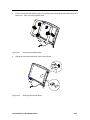
Disassembly and Unit Replacement
This chapter describes how to disassemble the 390 series notebook computer to make
replacements or upgrades.
Appendix A
Model Number Definition
This appendix shows the different configuration options for the 390 series notebook
computer.
Appendix B
Exploded View Diagram
This appendix illustrates the system board and CPU silk screens.
Appendix C
Spare Parts List
This appendix lists the spare parts for the 390 series notebook computer with their part
numbers and other information.
iii
Appendix D
Schematics
This appendix contains the schematic diagrams for the system board.
Appendix E
BIOS POST Checkpoints
This appendix lists and describes the BIOS POST checkpoints.
Conventions
The following are the conventions used in this manual:
Text entered by user
Represents text input by the user.
Screen messages
Denotes actual messages that appear onscreen.
,
,
, etc.
Represent the actual keys that you have to press on the
keyboard.
NOTE
Gives bits and pieces of additional information related to the
current topic.
WARNING
Alerts you to any damage that might result from doing or not
doing specific actions.
CAUTION
Gives precautionary measures to avoid possible hardware or
software problems.
IMPORTANT
Reminds you to do specific actions relevant to the
accomplishment of procedures.
TIP
Tells how to accomplish a procedure with minimum steps
through little shortcuts.
iv
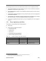
Table of Contents
Chapter 1
System Introduction
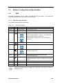
1.1
Overview ............................................................................................................. 1-1
1.2
System Board Layout........................................................................................... 1-2
1.2.1
Mainboard............................................................................................. 1-2
1.2.2
CPU Board............................................................................................ 1-4
1.2.3
Audio Board .......................................................................................... 1-5
1.2.4
Battery Board ........................................................................................ 1-5
1.2.5
Keyboard/Touchpad Board.................................................................... 1-6
1.3
Jumpers and Connectors ..................................................................................... 1-7
1.4
Hardware Configuration and Specification............................................................ 1-9
1.4.1
Memory Address Map ........................................................................... 1-9
1.4.2
Interrupt Channel Map........................................................................... 1-9
1.4.3
DMA Channel Map...............................................................................1-10
1.4.4
I/O Address Map ..................................................................................1-10
1.4.5
Processor.............................................................................................1-11
1.4.6
BIOS....................................................................................................1-11
1.4.7
System Memory ...................................................................................1-11
1.4.8
Second-Level Cache............................................................................1-12
1.4.9
Video Memory......................................................................................1-13
1.4.10
Video ...................................................................................................1-13
1.4.11
Parallel Port .........................................................................................1-14
1.4.12
Serial Port............................................................................................1-15
1.4.13
Audio ...................................................................................................1-15
1.4.14
PCMCIA...............................................................................................1-15
1.4.15
Touchpad.............................................................................................1-16
1.4.16
Keyboard .............................................................................................1-16
1.4.17
FDD .....................................................................................................1-17
1.4.18
HDD.....................................................................................................1-18
1.4.19
CD-ROM ..............................................................................................1-18
1.4.20
Battery .................................................................................................1-19
1.4.21
Charger................................................................................................1-19
1.4.22
DC-DC Converter.................................................................................1-20
1.4.23
DC-AC Inverter ....................................................................................1-21
v
1.5
1.6
1.4.24
LCD .....................................................................................................1-21
1.4.25
AC Adapter ..........................................................................................1-22
Software Configuration and Specification............................................................1-23
1.5.1
BIOS....................................................................................................1-23
1.5.2
Drivers, Applications and Utilities .........................................................1-29
Block Diagrams ..................................................................................................1-31
1.6.1
System.................................................................................................1-31
1.6.2
Clock ...................................................................................................1-32
1.7
Environmental Requirements..............................................................................1-33
1.8
Mechanical Specifications...................................................................................1-34
Chapter 2
2.1
2.2
2.3
2.4
2.5
vi
Major Chips Description
PCI 1250A ............................................................................................................2-2
2.1.1
Features.................................................................................................2-2
2.1.2
Block Diagram .......................................................................................2-4
2.1.3
Terminal Functions ................................................................................2-5
Aladdin IV (M1531/M1533) .................................................................................2-20
2.2.1
M1531..................................................................................................2-20
2.2.2
M1533..................................................................................................2-34
FDC37C672........................................................................................................2-47
2.3.1
Features...............................................................................................2-47
2.3.2
General Description .............................................................................2-49
2.3.3
Pin Configuration .................................................................................2-50
2.3.4
Pin Descriptions ...................................................................................2-52
2.3.5
Description of Multifunction Pins ..........................................................2-55
2.3.6
Block Diagram .....................................................................................2-56
65555 .................................................................................................................2-57
2.4.1
Features...............................................................................................2-57
2.4.2
Software Support Features...................................................................2-59
2.4.3
Introduction / Overview ........................................................................2-61
2.4.4
Pin Descriptions ...................................................................................2-63
M38813 ..............................................................................................................2-77
2.5.1
Overview .............................................................................................2-77
2.5.2
Description...........................................................................................2-77
2.6
2.5.3
Pin Configuration .................................................................................2-78
2.5.4
Pin Descriptions ...................................................................................2-79
YMF715B-S ........................................................................................................2-81
2.6.1
Features...............................................................................................2-81
2.6.2
Pin Diagram .........................................................................................2-82
2.6.3
Pin Descriptions ...................................................................................2-83
Chapter 3
BIOS Setup Utility
3.1
Basic System Settings ......................................................................................... 3-3
3.2
Startup Configuration ........................................................................................... 3-4
3.3
Onboard Devices Configuration ........................................................................... 3-6
3.4
System Security................................................................................................... 3-8
3.5
Power Management Settings ............................................................................... 3-9
3.6
Load Default Settings..........................................................................................3-11
Chapter 4
4.1
Disassembly and Unit Replacement
General Information ............................................................................................. 4-1
4.1.1
Before You Begin.................................................................................. 4-1
4.1.2
Connector Types................................................................................... 4-3
4.1.3
Disassembly Sequence ......................................................................... 4-4
4.2
Installing Memory................................................................................................. 4-6
4.3
Removing the Modem Board ............................................................................... 4-8
4.4
Removing the Hard Disk Drive............................................................................. 4-9
4.5
Removing the Keyboard .....................................................................................4-10
4.6
Disassembling the Inside Frame Assembly .........................................................4-12
4.7
4.6.1
Removing the Heat Sink Assembly ......................................................4-12
4.6.2
Removing the Display ..........................................................................4-13
4.6.3
Removing the Internal Drive.................................................................4-14
4.6.4
Replacing the CPU...............................................................................4-15
4.6.5
Detaching the Top Cover .....................................................................4-16
4.6.6
Removing the Mainboard .....................................................................4-17
4.6.7
Disassembling the Mainboard ..............................................................4-19
4.6.8
Disassembling the Top Cover ..............................................................4-20
Disassembling the Display ..................................................................................4-22
vii
Appendices
Appendix A
Model Number Definition
Appendix B
Exploded View Diagram
Appendix C
Spare Parts List
Appendix D
Schematics
Appendix E
BIOS POST Checkpoints
viii
List of Figures
1-1
PCB No. 96183-1A Mainboard Layout (Top) ........................................................ 1-2
1-2
PCB No. 96183-1A Mainboard Layout (Bottom) ................................................... 1-3
1-3
PCB No. 96534-SE CPU Board Layout (Top)....................................................... 1-4
1-4
PCB No. 96534-SE CPU Board Layout (Bottom).................................................. 1-4
1-5
PCB No. 97355-1 Audio Board............................................................................. 1-5
1-6
PCB No. 97348-1 Battery Board .......................................................................... 1-5
1-7
PCB No. 97349-1 Keyboard/Touchpad Board (Top View) .................................... 1-6
1-8
PCB No. 97349-1 Keyboard/Touchpad Board (Bottom View) ............................... 1-6
1-9
Jumpers and Connectors (Top View) ................................................................... 1-7
1-10
Jumpers and Connectors (Bottom View) .............................................................. 1-8
1-11
Power Management Block Diagram ....................................................................1-24
1-12
System Block Diagram........................................................................................1-31
1-13
Clock Block Diagram ..........................................................................................1-32
2-1
PCI1250 Block Diagram....................................................................................... 2-4
2-2
M1531 Pin Diagram (Top View) ..........................................................................2-23
2-3
M1533 Pin Diagram (Top View) ..........................................................................2-39
2-4
FDC37C67 (TQFP) Pin Diagram.........................................................................2-50
2-5
FDC37C67 (QFP) Pin Diagram...........................................................................2-51
2-6
FDC37C67 Block Diagram..................................................................................2-56
2-7
65555 BGA Ball Assignments (Top View) ...........................................................2-64
2-8
65555 BGA Ball Assignments (Bottom View) ......................................................2-65
2-9
M38813 Pin Diagram ..........................................................................................2-78
2-10
M38813 Block Diagram.......................................................................................2-80
2-11
YMF715 Block Diagram ......................................................................................2-82
4-1
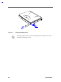
Removing the Battery Pack ................................................................................. 4-2
4-2
Using Connectors With Locks .............................................................................. 4-3
4-3
Disassembly Sequence Flowchart........................................................................ 4-5
4-4
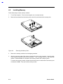
Removing the Memory Door ................................................................................ 4-6
4-5
Installing and Removing Memory......................................................................... 4-7
4-6
Removing the Modem Board ............................................................................... 4-8
4-7
Removing the Hard Disk Drive............................................................................. 4-9
4-8
Removing the Display Hinge Covers...................................................................4-10
4-9
Removing the Keyboard .....................................................................................4-10
4-10
Unplugging the Keyboard Connectors .................................................................4-11
ix
x
4-11
Removing the LED Cover ...................................................................................4-12
4-12
Removing the Heat Sink Assembly .....................................................................4-12
4-13
Unplugging the Display Cable .............................................................................4-13
4-14
Removing the Display Hinge Screws ..................................................................4-13
4-15
Removing the Display Hinge Screws ..................................................................4-14
4-16
Removing the Internal Drive ...............................................................................4-15
4-17
Replacing the CPU .............................................................................................4-15
4-18
Removing Cables ...............................................................................................4-16
4-19
Detaching the Top Cover ....................................................................................4-16
4-20
Removing the Bottom Screws.............................................................................4-17
4-21
Removing the Keyboard/Touchpad Board and DC-DC Converter Board Cover...4-17
4-22
Removing the DC-DC Converter Board ..............................................................4-18
4-23
Removing the Mainboard....................................................................................4-18
4-24
Removing the Charger Board .............................................................................4-19
4-25
Removing the PCMCIA Sockets .........................................................................4-19
4-26
Removing the Hard Disk Drive Heat Sink ...........................................................4-20
4-27
Removing the Audio Board .................................................................................4-20
4-28
Removing the Touchpad and Speakers ..............................................................4-21
4-29
Removing the LCD Bumpers ..............................................................................4-22
4-30
Removing the Display Bezel Screws...................................................................4-22
4-31
Removing the Display Bezel ...............................................................................4-23
4-32
Removing the Inverter Board ..............................................................................4-23
4-33
Removing the LCD Panel ...................................................................................4-24
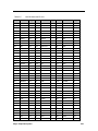
List of Tables
1-1
CPU Mounting Reference Table........................................................................... 1-5
1-2
SW1 Switch Settings ........................................................................................... 1-8
1-3
Memory Address Map .......................................................................................... 1-9
1-4
Interrupt Channel Map ......................................................................................... 1-9
1-5
DMA Channel Map..............................................................................................1-10
1-6
I/O Address Map .................................................................................................1-10
1-7
Processor Specifications.....................................................................................1-11
1-8
BIOS Specifications ............................................................................................1-11
1-9
Memory Configurations.......................................................................................1-12
1-10
Video RAM Configuration....................................................................................1-13
1-11
Video Hardware Specification .............................................................................1-13
1-12
Supported External CRT Resolutions..................................................................1-13
1-13
Supported LCD Resolutions ................................................................................1-14
1-14
Parallel Port Configurations ................................................................................1-14
1-15
Serial Port Configurations ...................................................................................1-15
1-16
Audio Specifications ...........................................................................................1-15
1-17
PCMCIA Specifications.......................................................................................1-16
1-18
Touchpad Specifications .....................................................................................1-16
1-19
Keyboard Specifications......................................................................................1-16
1-20
Windows 95 Key Descriptions .............................................................................1-17
1-21
FDD Specifications .............................................................................................1-17
1-22
HDD Specifications.............................................................................................1-18
1-23
CD-ROM Specifications ......................................................................................1-18
1-24
Battery Specifications .........................................................................................1-19
1-25
Charger Specifications........................................................................................1-20
1-26
DC-DC Converter Specifications.........................................................................1-20
1-27
DC-AC Inverter Specifications ............................................................................1-21
1-28
LCD Specifications .............................................................................................1-21
1-29
AC Adapter Specifications ..................................................................................1-22
1-30
Hotkey Descriptions ............................................................................................1-23
1-31
Standby Mode Conditions and Descriptions ........................................................1-25
1-32
Light Green Mode Conditions and Descriptions...................................................1-26
1-33
Hibernation Mode Conditions and Descriptions ...................................................1-27
1-34
Display Standby Mode Conditions and Descriptions ............................................1-27
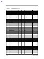
xi
xii
1-35
Hard Disk Standby Mode Conditions and Descriptions ........................................1-28
1-36
Location of Drivers in the System Utility CD........................................................1-29
1-37
Location of Applications in the System Utility CD ................................................1-30
1-38
Environmental Requirements..............................................................................1-33
1-39
Mechanical Specifications...................................................................................1-34
2-1
Major Chips List ....................................................................................................2-1
2-2
PCI1250 Terminal Functions.................................................................................2-5
2-3
M1531 Signal Descriptions..................................................................................2-24
2-4
M1531 Numerical Pin List ...................................................................................2-28
2-5
M1533 Numerical Pin List ...................................................................................2-40
2-6
FDC37C67 Pin Descriptions ...............................................................................2-52
2-7
FDC37C67 Multifunction Pin Descriptions...........................................................2-55
2-8
65555 Pin Functions ...........................................................................................2-66
2-9
M38813M4-XXXHP Functions.............................................................................2-77
2-10
M38813M4-XXXHP Pin Description ....................................................................2-79
2-11
YMF715 Descriptions..........................................................................................2-83
3-1
Basic System Settings Parameters .......................................................................3-3
3-2
Startup Configuration Parameters.........................................................................3-4
3-3
Onboard Devices Configuration Parameters .........................................................3-6
3-4
System Security Parameters.................................................................................3-8
3-5
Power Management Settings Parameters .............................................................3-9
4-1
Guide to Disassembly Sequence ..........................................................................4-4
B-1
Exploded View Diagram List ................................................................................ B-1
C-1
Spare Parts List ................................................................................................... C-1
D-1
Schematics List ................................................................................................... D-1
E-1
POST Checkpoint List.......................................................................................... E-1
C h a p t e r
1
System Introduction
1.1
Overview
This computer combines high-performance, versatility, power management features and
multimedia capabilities with unique style and ergonomic design. This computer was designed with
the user in mind. Here are just a few of its many features:
•
Performance
• Intel Pentium® processor with MMX™ technology
• 64-bit main memory and external (L2) cache memory
• Large LCD display and PCI local bus video with graphics acceleration
• Internal CD-ROM drive and external 3.5-inch floppy drive, or internal 3.5-inch floppy drive
• High-capacity, Enhanced-IDE hard disk
• Lithium-Ion or Nickel Metal-Hydride battery pack
• Power management system with light green, standby and hibernation power saving modes
•
Multimedia
• 16-bit high-fidelity stereo audio with 3-D sound
• Built-in dual speakers
• Ultra-slim, high-speed CD-ROM drive
•
Connectivity
• High-speed fax/data modem port
• Fast infrared wireless communication
• USB (Universal Serial Bus) port
•
Human-centric Design and Ergonomics
• Lightweight and slim
• Sleek, smooth and stylish design
• Full-sized keyboard and wide palmrest
• Ergonomically-centered touchpad pointing device
•
Expansion
• CardBus PC card (formerly PCMCIA) slots (two type II/I or one type III) with ZV (Zoomed
Video) port support
• Port replicator option for one-step connect/disconnect from peripherals
• User-upgradeable memory and hard disk
System Introduction
1-1
1.2
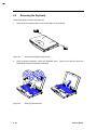
System Board Layout
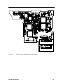
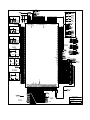
1.2.1
Mainboard
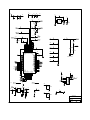
Figure 1-1
1-2
PCB No. 96183-1A Mainboard Layout (Top)
Service Guide
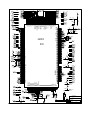
Figure 1-2
PCB No. 96183-1A Mainboard Layout (Bottom)
System Introduction
1-3
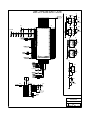
1.2.2
CPU Board
Figure 1-3
PCB No. 96534-SE CPU Board Layout (Top)
Figure 1-4
PCB No. 96534-SE CPU Board Layout (Bottom)
1-4
Service Guide
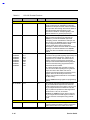
The following table is a reference when mounting1 the CPU.
Table 1-1
CPU Mounting Reference Table
Volt.
CPU
Ratio
Freq
R4
R6
R8
R11 R20 R22 R24 R26 RX14 RY1 RX6
RX9
RX11 RX12 UX2 UX3
P55C-133MHz 2.5V
133=66x2
V
X
V
X
V
X
X
V
V
X
V
X
X
X
X
X
P55C-150MHz 2.5V
150=60x2.5
V
X
V
V
X
X
V
V
V
X
V
X
X
X
X
X
P55C-166MHz 2.5V
166=66x2.5
V
X
V
X
X
X
V
V
V
X
V
X
X
X
X
X
TLMK-200MHz 1.8V
200=66x3
X
X
V
X
X
V
V
X
V
X
X
V
V
V
V
V
TLMK-233MHz 1.8V
233=66x3.5
X
X
V
X
V
V
X
X
V
X
X
V
V
V
V
V
TLMK-266MHz 2.0V
266=66x4
X
V
V
X
X
X
V
V
X
V
X
V
V
V
V
V
1.2.3
Volt
Ext Freq
Audio Board
Figure 1-5
1.2.4
Battery Board
Figure 1-6
1
PCB No. 97355-1 Audio Board
PCB No. 97348-1 Battery Board
V: mount on; X: not mount on
System Introduction
1-5
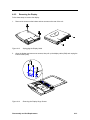
1.2.5
Keyboard/Touchpad Board
Figure 1-7
PCB No. 97349-1 Keyboard/Touchpad Board (Top View)
Figure 1-8
PCB No. 97349-1 Keyboard/Touchpad Board (Bottom View)
1-6
Service Guide
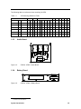
1.3
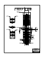
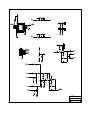
Jumpers and Connectors
TOP VIEW
CN1
CN4
CN5
CN8
CN12
CN2
CN3
CN6
U1
CN7
CN11
CN9
CN10
CN16
CN13
CN15
CN14
SW1
CN17
CN18
CN21
CN19
CN20
CN22
GF1
CN1
CN2
CN3
CN4
CN5
CN6
CN7
CN8
CN9
CN10
CN11
CN12
CN13
USB port
Parallel port
Serial port
VGA port
Port replicator port
RJ-11 phone jack
DC-DC connector
Inverter connector
LCD connector
Charger connector
Charger connector
Fan connector
Internal speaker connector (left)
Figure 1-9
CN14
CN15
CN16
CN17
CN18
CN19
CN20
CN21
CN22
GF1
SW1
U1
Audio board cable connector
Internal speaker connector (right)
PCMCIA socket connector
FDD/CD-ROM connector
Internal keyboard/touchpad connector
HDD connector
CD-ROM connector
CPU board connector
Battery connector
Golden finger for debug card
KB/password/logo setting switch
FIR port
Jumpers and Connectors (Top View)
System Introduction
1-7
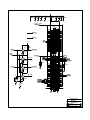
BOTTOM VIEW
CN24
CN23
DIMM
CN23
CN24
DIMM
Modem connector
Modem connector
DIMM sockets
Figure 1-10
Jumpers and Connectors (Bottom View)
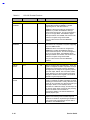
The following tables list the switch settings for SW1.
Table 1-2
SW1 Switch Settings
ON
OFF
Switch 1 (Logo Screen)
OEM
Acer
Switch 2 (Password)
Bypass
Check
Germany
U.S.
Japanese
Switch 3 (KB Language)
On
Off
Off
Switch 4 (KB Language)
Off
Off
On
1-8
Service Guide
1.4
Hardware Configuration and Specification
1.4.1
Memory Address Map
Table 1-3
Memory Address Map
Address Range
Definition
Function
000000 - 09FFFF
640 KB memory
Base memory
0A0000 - 0BFFFF
128 KB video RAM
Reserved for graphics display buffer
0C0000 - 0CBFFF
Video BIOS
Video BIOS
0F0000 - 0FFFFF
64 KB system BIOS
System BIOS
100000 - top limited
Extended memory
SIMM memory
FE0000 - FFFFFF
256 KB system ROM
Duplicate of code assignment at 0E0000-0FFFFF
1.4.2
Table 1-4
Priority
1
2
3
4
5
6
7
8
9
10
11
12
13
14
15
16
17
18
19
Interrupt Channel Map
Interrupt Channel Map
Interrupt Number
SMI
NMI
IRQ 0
IRQ 1
IRQ 2
IRQ 8
IRQ 9
IRQ 10
IRQ 11
IRQ 12
IRQ 13
IRQ 14
IRQ 15
IRQ 3
IRQ 4
IRQ 5
IRQ 6
IRQ 7
System Introduction
Interrupt Source
Power management unit
Parity error detected, I/O channel error
Interval timer, counter 0 output
Keyboard
Interrupt from controller 2 (cascade)
Real-time clock /
Cascaded to INT 0AH (IRQ 2) / Audio / PCMCIA
Audio (option) / PCMCIA / Internal modem / Serial
communication port 2 / PCMCIA / USB
Audio (option) / PCMCIA / Internal modem / Serial
communication port 1 / PCMCIA
PS/2 mouse
INT from coprocessor
Hard disk controller / PCMCIA controller
CD-ROM controller / PCMCIA controller
Serial communication port 2 / Internal modem / Audio / PCMCIA
Serial communication port 1 / Internal modem / Audio / PCMCIA
Parallel port (option) / Internal modem / Audio / PCMCIA
Diskette controller
Parallel port (option) / Audio
1-9
1.4.3
DMA Channel Map
Table 1-5
DMA Channel Map
Controller
Channel
Address
Function
1
1
1
1
2
2
2
2
0
1
2
3
4
5
6
7
0087
0083
0081
0082
Cascade
008B
0089
008A
Audio (option) / Audio
Audio (option) / ECP / Audio / FIR
Diskette
Audio (option) / ECP / FIR
Cascade
Not support
Not support
Not support / Audio
1.4.4
I/O Address Map
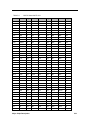
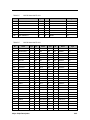
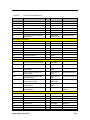
Table 1-6
I/O Address Map
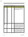
Address Range
000 - 00F
020 - 021
040 - 043
048 - 04B
060 - 06E
070 - 071
080 - 08F
0A0 - 0A1
0C0 - 0DF
1F0 - 1F7
220 - 22F
230 - 23F
240 - 24F
250 - 25F
278 - 27F
2E8 - 2EF
2F8 - 2FF
378, 37A
3BC - 3BE
3B4, 3B5, 3BA
3C0 - 3C5
3C6 - 3C9
3C0 - 3CF
3D0 - 3DF
3E0 - 3E1
3E8 - 3EF
3F0 - 3F7
3F8 - 3FF
CF8 - CFF
1-10
Device
DMA controller-1
Interrupt controller-1
Timer 1
Timer 2
Keyboard controller 8742 chip select
Real-time clock and NMI mask
DMA page register
Interrupt controller-2
DMA controller-2
Hard disk select
Audio (option) - default
Audio (option)
Audio (option)
Audio (option)
Parallel port 3
COM 4
COM 2
Parallel port 2
Parallel port 1
Video subsystem
Video subsystem
Video DAC
Enhanced graphics display
Color graphics adapter
PCMCIA controller
COM3
Floppy disk controller
COM 1
PCI configuration register
Service Guide
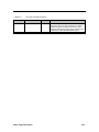
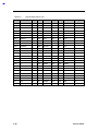
1.4.5
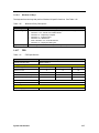
Processor
Table 1-7
Processor Specifications
Item
Specification
CPU type
P55C-133/150/166
CPU package
TCP
Switchable processor speed (Y/N)
Yes
Minimum working speed
0MHz
CPU core voltage
2.0V/2.45V/1.8V
CPU I/O voltage
2.5V/3.3V/2.5V
1.4.6
BIOS
Table 1-8
BIOS Specifications
Item
Specification
BIOS vendor
Acer
BIOS version
V3.0
BIOS in flash EPROM (Y/N)
Yes
BIOS ROM size
256KB
BIOS package type
32-pin PLCC
Same BIOS for STN color/TFT color (Y/N)
Yes
The BIOS can be overwritten/upgradeable using the “AFLASH”
(AFLASH.EXE). Please refer to software specification section for details.
1.4.7
utility
System Memory
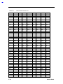
Memory is upgradeable from 8 to 64 MB, employing 8-/16-/32-/64-MB2 64-bit soDIMMs (Small
Outline Dual Inline Memory Modules). After installing the memory modules, the system
automatically detects and reconfigures the total memory size during the POST routines. The
following lists important memory specifications.
•
•
•
Memory bus width: 64-bit
Expansion RAM module type:144-pin, 64-bit, small outline Dual Inline Memory Module
(soDIMM)
Expansion RAM module size/configuration:
• 8MB (1M*16x4)
2
You can upgrade memory using 32-MB soDIMMs when these become available. Consult your dealer.
System Introduction
1-11
• 16MB (2M*8x8)
• 32MB (4M*16x4)
• 64MB (8M*8x8)
•
Expansion RAM module speed/voltage/package: 60ns/3.3v/TSOP EDO
•
EDO and fast-page mode DIMMs may be used together in a memory configuration.
The following table lists all possible memory configurations.
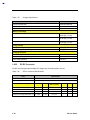
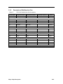
Table 1-9
1.4.8
Memory Configurations
Slot 1
Slot 2
Total Memory
8 MB
0 MB
8 MB
0 MB
8 MB
8 MB
8 MB
8 MB
16 MB
16 MB
0 MB
16 MB
0 MB
16 MB
16 MB
16 MB
8 MB
24 MB
8 MB
16 MB
24 MB
16 MB
16 MB
32 MB
32 MB
0 MB
32 MB
0 MB
32 MB
32 MB
32 MB
8 MB
40 MB
8 MB
32 MB
40 MB
32 MB
16 MB
48 MB
16 MB
32 MB
48 MB
32 MB
32 MB
64 MB
64MB
0MB
64MB
0MB
64MB
64MB
64MB
8MB
72MB
8MB
64MB
72MB
64MB
16MB
80MB
16MB
64MB
80MB
64MB
32MB
96MB
32MB
64MB
96MB
64MB
64MB
128MB
Second-Level Cache
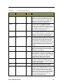
This notebook has 256KB second-level (L2) cache onboard.
1-12
Service Guide
1.4.9
Video Memory
Table 1-10
Video RAM Configuration
Item
Specification
DRAM or VRAM
DRAM(EDO type)
Fixed or upgradeable
Fixed
Memory size/configuration
2MB (256K x 16 x 4pcs)
Memory speed
50ns
Memory voltage
3.3V
Memory package
TSOP
1.4.10
Video
Table 1-11
Video Hardware Specification
Item
Specification
Video chip
C&T65555
Working voltage
3.3V
1.4.10.1
External CRT Resolution Support
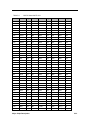
Table 1-12
Supported External CRT Resolutions
Resolution x Color on
External CRT
CRT Refresh Rate
Simultaneous on
TFT LCD
Simultaneous on
STN LCD
CRT only
Simultaneous
SVGA
SVGA
640x480x16
60,75,85
60
Y
Y
640x480x256
60,75,85
60
Y
Y
640x480x65,536
60,75,85
60
Y
Y
640x480x16,777,216
60,75,85
60
Y
Y
800x600x16
56,60,75,85
60
Y
Y
800x600x256
56,60,75,85
60
Y
Y
800x600x65,536
56,60,75,85
60
Y
Y
800x600x16,777,216
56,60,75,85
60
Y
Y
1024x768x16
60,75,85,86I
60
Y
Y
1024x768x256
60,75,85,86I
60
Y
Y
1024x768x65536
60,75,85,86I
60
Y
Y
1280x1024x16
60,75,86I
60
Y
Y
1280x1024x256
60,75,86I
60
Y
Y
System Introduction
1-13
1.4.10.2
LCD Resolution Support
Table 1-13
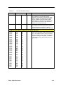
Supported LCD Resolutions
Resolution x Color on LCD Only
TFT LCD (SVGA)
DSTN LCD (SVGA)
640x480x16
Y
Y
640x480x256
Y
Y
640x480x65,536
Y
Y
640x480x16,777,216
Y
Y
800x600x16
Y
Y
800x600x256
Y
Y
800x600x65,536
Y
Y
800x600x16777216
Y
Y
1024x768x16
Y
Y
1024x768x256
Y
Y
1024x768x65536
Y
Y
1280x1024x16
Y
Y
1280x1024x256
Y
Y
•
Maximum resolution (External CRT): 1280x1024
Using software, you can set the LCD to a higher resolution than its physical
resolution, but the image shown on the LCD will pan.
1.4.11
Parallel Port
Table 1-14
Parallel Port Configurations
Item
Specification
Number of parallel ports
1
ECP support
Yes (set by BIOS setup)
Connector type
25-pin D-type
Location
Rear side
Selectable parallel port (by BIOS Setup)
•
•
•
•
1-14
Parallel 1 (3BCh, IRQ7)
Parallel 2 (378h, IRQ7)
Parallel 3 (278h, IRQ5)
Disable
Service Guide
1.4.12
Serial Port
Table 1-15
Serial Port Configurations
Item
Specification
Number of serial ports
1
16550 UART support
Yes
Connector type
9-pin D-type
Location
Rear side
Selectable serial port (by BIOS Setup)
•
•
•
1.4.13
Serial 1 (3F8h, IRQ4)
Serial 2 (2F8h, IRQ3)
Disable
Audio
Table 1-16
Audio Specifications
Item
Specification
Chipset
YMF715
Audio onboard or optional
Built-in
Mono or stereo
Stereo
Resolution
16-bit
Compatibility
SB-16 , Windows Sound System
Mixed sound sources
Voice, Synthesizer, Line-in, Microphone, CD
Voice channel
8-/16-bit, mono/stereo
Sampling rate
44.1 kHz
Internal microphone
No
Internal speaker / quantity
Yes / 2 pcs.
Microphone jack
Yes
Headphone jack
Yes
1.4.14
PCMCIA
PCMCIA is an acronym for Personal Computer Memory Card International Association. The
PCMCIA committee set out to standardize a way to add credit-card size peripheral devices to a
wide range of personal computers with as little effort as possible.
There are two type II/I or one type III PC Card slots found on the left panel of the notebook. These
slots accept credit-card-sized cards that enhances the usability and expandability of the notebook.
ZV (Zoomed Video) port support allows your system to support hardware MPEG in the form of a
ZV PC card.
System Introduction
1-15
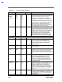
Table 1-17
PCMCIA Specifications
Item
Specification
Chipset
TI 1250A
Supported card type
Type-II / Type-III
Number of slots
Two Type-II or one Type-III
Access location
Left side
ZV (Zoomed Video) port support
Yes
1.4.15
Table 1-18
Touchpad
Touchpad Specifications
Item
Specification
Vendor & model name
Synaptics TM3202TPD-226
Power supply voltage (V)
5 ± 10%
Location
Palm-rest center
Internal & external pointing device work simultaneously
Yes
Support external pointing device hot plug
Yes
X/Y position resolution (points/mm)
20
Interface
PS/2 (compatible with Microsoft mouse driver)
1.4.16
Table 1-19
Keyboard
Keyboard Specifications
Item
Specification
Vendor & model name
SMK KAS1901-0161R (English)
Total number of keypads
84/85 keys
Windows 95 keys
Yes, (Logo key / Application key):
Internal & external keyboard work simultaneously
Yes
1-16
Service Guide
1.4.16.1
Windows 95 Keys
The keyboard has two keys that perform Windows 95-specific functions. See Table 1-26.
Table 1-20
Windows 95 Key Descriptions
Key
Description
Windows logo key
Application key
1.4.17
Start button. Combinations with this key performs special functions, e.g.:
•
Windows + Tab Activate next Taskbar button
•
Windows + E Explore My Computer
•
Windows + F Find Document
•
Windows + M Minimize All
•
Shift + Windows + M Undo Minimize All
•
Windows + R Display Run dialog box
Opens the application’s context menu (same as right-click).
FDD
Table 1-21
FDD Specifications
Item
Vendor & model name
Specification
Mitsumi D353F2
Floppy Disk Specifications
Media recognition
2DD (720K)
2HD (1.2M, 3-mode)
2HD (1.44M)
Sectors / track
9
15
18
Tracks
80
80
80
500
500
360
300
Data transfer rate (Kbits/s)
250
300
Rotational speed (RPM)
300
360
Read/write heads
2
Encoding method
MFM
Power Requirement
Input Voltage (V)
System Introduction
+5 ± 10%
1-17
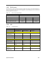
1.4.18
HDD
Table 1-22
HDD Specifications
Item
Vendor & Model Name
Specification
Hitachi DK225A-21
IBM DTNA22160
IBM DDLA21620
Capacity (MB)
2160
2160
1620
Bytes per sector
512
512
512
Logical heads
16
16
16
Logical sectors
63
63
63
Logical cylinders
4889
4200
3152
Physical read/write heads
6
6
3
Disks
3
3
2
Spindle speed (RPM)
4464
4000
4000
Buffer size (KB)
128
96
96
Interface
ATA-3(IDE)
ATA-2
ATA-2
Data transfer rate
(disk-buffer, Mbytes/s)
5.7 ~ 9.0
5 ~ 7.7
5 ~ 8.3
Data transfer rate
(host-buffer, Mbytes/s)
16.6 /33.3
(max., PIO mode 4)
16.6
(max., PIO mode 4)
16.6
(max., PIO mode 4)
5 ± 5%
5 + 5%
5 ± 5%
Drive Format
Performance Specifications
DC Power Requirements
Voltage tolerance (V)
1.4.19
CD-ROM
Table 1-23
CD-ROM Specifications
Item
Vendor & Model Name
Specification
Panasonic KMEUJDA110
Performance Specification
Speed (KB/sec)
2100 (14X ave. speed)
Access time (ms)
150 (Typ.)
Buffer memory (KB)
128
Interface
Enhanced IDE (ATAPI) compatible
Applicable disc format
CD-DA, CD-ROM, CD-ROM XA (except ADPCM), CD-I, Photo CD
(Multisession), Video CD, CD+
Loading mechanism
Soft eject (with emergency eject hole)
Power Requirement
Input Voltage (V)
1-18
5
Service Guide
1.4.20
Battery
Table 1-24
Battery Specifications
Item
Specification
Battery gauge on screen
Yes, by hotkey
Yes, by hotkey
Vendor & model name
Toshiba BTP-031
Sony BTP-T31
Battery type
NiMH
Li-Ion
Cell capacity (mAH)
3500
1400
Cell voltage (V)
1.2
3.6
Number of battery cell
9-cell
9-Cell
Package configuration
9 serial
3 serial, 3 parallel
Package voltage (V)
10.8
10.8
Package capacity (WAH)
3500
4200
Second battery
No
No
1.4.21
Charger
To charge the battery, place the battery pack inside the battery compartment and plug the AC
adapter into the notebook and an electrical outlet. The adapter has three charging modes:
•
Rapid mode
The notebook uses rapid charging when power is turned off and a powered AC adapter is
connected to it. In rapid mode, a fully depleted battery gets fully charged in approximately two
hours.
•
Charge-in-use mode
When the notebook is in use with the AC adapter plugged in, the notebook also charges the
battery pack if installed. This mode will take longer to fully charge a battery than rapid mode.
In charge-in-use mode, a fully depleted battery gets fully charged in approximately six to eight
hours.
•
Trickle mode
The adapter charges the battery pack for two hours using trickle current 380mA, then shifts to
1/10 duty pulse trickle charge to keep the battery capacity at 100%.
System Introduction
1-19
Table 1-25
Charger Specifications
Item
Specification
Vendor & model name
Ambit T62.069.C.00
Input voltage (from adapter, V)
0-24V
Output current (to DC/DC converter, A)
3 (max.)
Battery Low Voltage
Battery Low 1 level (V)
10.16 (typ., for NiMH)
8.566 (typ., for LIB)
Battery Low 2 level (V)
10.279 (typ., for NiMH)
8.185 (typ., for LIB)
Battery Low 3 level (V)
9.137 (typ., for NiMH)
7.709 (typ., for LIB)
Charge Current
Background charge (charge even system is still operative, A)
0.8 (typ.)
Normal charge (charge while system is not operative, A)
2.0 (typ.)
Charging Protection
Maximum temperature protection (ºC)
60
Maximum voltage protection (V)
16.7V±0.2V
Over voltage protection
13V±0.15
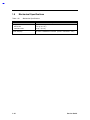
1.4.22
DC-DC Converter
DC-DC converter generates multiple DC voltage level for whole system unit use.
Table 1-26
DC-DC Converter Specifications
Item
Specification
Vendor & model name
Ambit T62.041.C.00
Input voltage (Vdc)
8~21
Output Rating
Current (w/ load, A)
Voltage ripple (max., mV)
Voltage noise (max., mV)
OVP (Over Voltage Protection, V)
1-20
5V
3.3V
2.9V
(2.9 /3.1 /3.3V)
+12V
+6V
5VSB
0~3.2
0~3.3
0~4.2
0~0.15
0~0.1
0.005
50
50
50
100
300
75
100
100
100
200
500
250
6.1~8.0
4.2~6.2
3.3-5.2 V
-
-
-
Service Guide
1.4.23
DC-AC Inverter
DC-AC inverter is used to generate very high AC voltage, then supply to LCD CCFT backlight use,
and is also responsible for the control of LCD brightness. Avoid touching the DC-AC inverter area
while the system unit is turned on.
Table 1-27
DC-AC Inverter Specifications
Item
Specification
Vendor & model name
Ambit T62.071.C.00
Input voltage (V)
6.8(in.)
-
22(max.)
-
-
750 (max.)
Output voltage (Vrms, no load)
1000 (min.)
-
1600 (max.)
Output voltage frequency (kHz)
40 (min.)
-
65 (max.)
1.0~5.5 (min.)
1.5~6.1 (typ.)
2.0~6.7 (max.)
Input current (mA)
Output current (mArms)
1.4.24
LCD
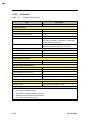
Table 1-28
LCD Specifications
Item
Specification
Vendor & model name
HITACHI
LMG9980ZWCC-01
TORiSAN
LM-JK53-22NFR-A
HITACHI
TX31D21VC
Mechanical Specifications
LCD display area
(diagonal, inch)
12.1
12.1
12.1
Display technology
STN
STN
TFT
Resolution
SVGA (800x600)
VGA (800x600)
SVGA (800x600)
Supported colors
--
--
262,144 colors
35 (typ.)
40 (typ.)
80 (typ.)
Brightness (cd/m )
70 (typ.)
70 (typ.)
70 (typ.)
Brightness control
keyboard hotkey
keyboard hotkey
keyboard hotkey
Contrast control
using keyboard
hotkey
using keyboard
hotkey
none
Supply voltage for LCD
display (V)
3.3 or 5 (typ.)
3.3 or 5 (typ.)
3.0 ~ 3.6 (typ.)
Supply voltage for LCD
backlight (Vrms)
650 (typ.)
630 (typ.)
595(typ.), 660(max)
Optical Specification
Contrast ratio
2
Electrical Specification
System Introduction
1-21
1.4.25
AC Adapter
Table 1-29
AC Adapter Specifications
Item
Vendor & model name
Specification
Delta ADP-45GB Rev. E3, E5
Input Requirements
Nominal voltages (Vrms)
90 - 264
Nominal frequency (Hz)
47 - 63
Frequency variation range (Hz)
47 - 63
Maximum input current (A, @90Vac, full load)
1.5 A
Inrush current
The maximum inrush current will be less than 50A and
100A when the adapter is connected to 115Vac(60Hz)
and 230Vac(50Hz) respectively.
Efficiency
It should provide an efficiency of 83% minimum, when
measured at maximum load under 115V(60Hz).
Output Ratings (CV mode)
DC output voltage (V)
+19.0V~20.5V
Noise + Ripple (mV)
300mvp-pmax (20Mhz bandwidth)
Load (A)
0 (min.)
2.4 (max.)
Output Ratings (CC mode)
DC output voltage (V)
+12 ~+19
Constant output (A)
2.75 ± 0.2
Dynamic Output Characteristics
Turn-on delay time (s, @115Vac)
2
Hold up time (ms; @115 Vac input, full load)
5 (min.)
Over Voltage Protection (OVP, V)
26
Short circuit protection
Output can be shorted without damage
Electrostatic discharge (ESD, kV)
±15 (at air discharge)
Dielectric Withstand Voltage
Primary to secondary
3000 Vac (or 4242 Vdc), 10 mA for 1 second
Leakage current
0.25 mA maximum @ 254 Vac, 60Hz.
Regulatory Requirements
Internal filter meets:
1.
FCC class B requirements. (USA)
2.
VDE 243/1991 class B requirements. (German)
3.
CISPR 22 Class B requirements. (Scandinavia)
4.
VCCI class II requirements. (Japan)
1-22
Service Guide
1.5
Software Configuration and Specification
1.5.1
BIOS
The BIOS is compliant to PCI v2.1, APM v1.2, E-IDE and PnP specification. It also defines the
hotkey functions and controls the system power-saving flow.
1.5.1.1
Keyboard Hotkey Definition
The notebook supports the following hotkeys.
Table 1-30
Hotkey
Hotkey Descriptions
Icon
Function
Description
Fn-Esc
Hotkey Escape
Exits the hotkey control.
Fn-F1
Hotkey Help
Displays the hotkey list and help. Press | to exit the screen.
Brightness Control
Toggles between brightness control and contrast control.
Fn-F2
?
Press the scale hotkeys (Fn- →and Fn -←) to increase and
decrease the brightness or contrast level.
Contrast Control
Notebooks with TFT displays do not show the brightness
control icon.
Fn-F3
Display Toggle
Switches display from LCD to CRT to both LCD and CRT.
Fn-F4
Battery Gauge
Displays the battery gauge.
Fn-F5
Volume Control
Press the scale hotkeys (Fn-→ and Fn-←) to increase and
decrease the output level.
Fn-F6
Setup
Gains access to BIOS Setup’s Advanced System
Configuration parameters.
Fn-F7
Hibernation/Standb
y
Enters hibernation mode if the 0-volt suspend function is
installed and enabled; otherwise, the notebook enters standby
mode.
Fn-→
Scale Increase
Increases the setting of the current icon.
Fn-←
Scale Decrease
Decreases the setting of the current icon.
Fn-T
Toggle Touchpad
Turns the internal touchpad on and off.
When the available hotkey is toggled, the system will issue a beep to enter the
assigned process.
System Introduction
1-23
1.5.1.2
MultiBoot
The system can boot from the FDD, External FDD, HDD, CD-ROM. The user can select the
desired booting process to boot the system. If the CD-ROM is bootable, the BIOS will override the
other process to boot the system directly.
1.5.1.3
Power Management
This computer has a built-in power management unit that monitors system activity. System activity
refers to any activity involving one or more of the following devices: keyboard, mouse, floppy drive,
hard disk, peripherals connected to the serial and parallel ports, and video memory. If no activity is
detected for a period of time (called an inactivity time-out), the computer stops some or all of these
devices in order to conserve energy.
This computer employs an innovative power management technique called Heuristic Power
Management or HPM. HPM allows the computer to provide maximum power conservation and
maximum performance at the same time.
Power management methods used by most computers are timer-based. You set inactivity time-out
values for the display, hard disk, and other devices. The computer then "sleeps" when these timeouts elapse. The problem with this is that no two users are alike. Each of us has his or her own
habits when using the computer, which makes timer-based power management ineffective.
With HPM, your computer manages its power according to the way you use your computer. This
means the computer delivers maximum power when you need it, and saves power when you don’t
need the maximum — all without your intervention. There are no timers to set, because the HPM
system figures out everything for you.
Cover Door Close
Power Switch Off More than 3 Seconds
Power Off
Power Switch On
Display Screen Off
Check password if needed
K/B, PS/2 Mouse Pressed
System Active
Display Standby
Timer Time Out
Power Switch (Beep)
Standby Event
Normal Mode
Hibernation
Event
Standby Mode
Light Green Mode
Cover Door Close
Hibernation Mode
HDD Standby Timer Time Out
Idle of HDD
1-24
Event
Power Switch (Beep)
Power Switch
Standby Mode
Figure 1-11
Standby Wakeup
Cover Door Open
Light Green Mode
HDD Standby Mode
(HDD Motor Off)
HDD Acess
Power Management Block Diagram
Service Guide
ON MODE
Normal full-on operation
STANDBY MODE
The computer consumes very low power in standby mode.
memory until battery is drained.
Data remain intact in the system
Warning: Unstored data is lost when you turn off the computer power in standby
mode or when the battery is drained.
Table 1-31
Standby Mode Conditions and Descriptions
Condition
The condition
to enter
Standby Mode
Description
There are two necessary conditions for the computer to enter standby mode:
•
Heuristic Power Management Mode must be set to [ENABLED].
•
System Sleep State must be set to [STANDBY].
In this situation, the following are ways to enter standby mode:
•
•
•
•
Pressing the sleep hot key Fn-F7
If the waiting time determined by the computer’s HPM unit elapses without any
system activity.
Closing the display cover.
With the System Sleep State is set to [HIBERNATION], the computer also enters
standby mode if the hibernation file (Sleep Manager) is invalid or not present.
•
“Hard Disk Drive” is [Disabled] in System Security of BIOS SETUP.
•
“Hard Disk 0” is [None] in Basic System Configuration of BIOS SETUP.
Note: If the computer detects a PC I/O card installed in the PC card slots, the computer
"sleeps" (light green mode) to maintain your communications connection. It will not enter
standby mode.
The condition
of Standby
Mode
•
•
•
•
•
•
The condition
back to On
Mode
Any one of following activities will let system back to Normal Mode:
•
Any keystroke (Internal KB or External KB)
•
Any active pointing device (internal or external, PS/2 or serial or USB)
•
Resume Timer matched
•
Opening the display cover if you closed the display cover to enter Standby mode.
•
Modem ring
Issue a beep.
Light standby LED with 1 Hz frequency.
Disable the mouse, serial and the parallel port.
The keyboard controller, HDD and VGA enter the standby mode.
Stop the CPU internal clock.
All the functions are disabled except the keyboard, battery low warning and modem
ring wake up from standby (if enabled).
System Introduction
1-25
LIGHT GREEN MODE
The notebook consumes very low power in light green mode. Data and I/O connections remain
intact in the system memory until battery is drained.
Table 1-32
Light Green Mode Conditions and Descriptions
Condition
Description
The condition to enter
Light Green Mode
•
•
PCMCIA I/O Card detected and occupy resources (Non Cardbus mode).
HPM timer times out or cover close or APM standby / suspend function calls.
The condition of Light
Green Mode
•
•
Issue a beep.
Only HDD, VGA enter standby
The condition back to
On Mode
Any one of following activities will let system back to Normal Mode:
•
Any keystroke (Internal KB or External KB)
•
Modem ring.
HIBERNATION MODE
In hibernation mode, all power shuts off (the computer does not consume any power). The
computer saves all system information onto the hard disk before it enters hibernation mode. Once
you turn on the power, the computer restores this information and resumes where you left off upon
leaving hibernation mode.
If the computer beeps but does not enter hibernation mode after pressing the sleep
hot key, it means the operating system will not allow the computer to enter the
power saving mode.
Do not change any devices (such as add memory or swap hard disks when the
computer is in hibernation mode.
If the computer detects a PC I/O card installed in the PC card slots, the computer
enters light green mode to maintain your communications connection. It will not
enter standby nor hibernation mode.
1-26
Service Guide
Table 1-33
Hibernation Mode Conditions and Descriptions
Condition
Description
The condition to
enter Hibernation
Mode
There are two necessary conditions for the computer to enter standby mode:
•
Heuristic Power Management Mode must be set to [ENABLED].
•
System Sleep State must be set to [HIBERNATION].
•
The hibernation file created by Sleep Manager must be present and valid.
In this situation, the following are ways to enter hibernation mode:
The condition of
Hibernation Mode
•
Pressing the sleep hot key Fn-F7
•
“Hard Disk Drive” is not [Disabled] in System Security of BIOS SETUP.
•
“Hard Disk 0” is not [None] in Basic System Configuration of BIOS SETUP.
•
If the waiting time determined by the computer’s HPM unit elapses without any
system activity.
•
If a battery low condition takes place, the computer enters hibernation mode in
about three minutes. The Sleep Upon Battery-low parameter in Setup must be
set to [ENABLED].
•
Invoked by the operating system power saving modes
•
Except the RTC, KB controller and power switch, all the system components are
off.
The condition back •
to On Mode
•
Pressing the power switch.
Resume Timer matched
DISPLAY STANDBY MODE
Screen activity is determined by the keyboard, the built-in touchpad, and an external PS/2 pointing
device. If these devices are idle for the period determined by the computer’s HPM unit, the display
shuts off until you press a key or move the touchpad or external mouse.
Table 1-34
Display Standby Mode Conditions and Descriptions
Condition
Description
The condition to enter
Display Standby Mode
•
Pointing device is idle until Display Standby Timer times-out or LCD cover
is closed.
The condition of
Display Standby Mode
•
All the system components are on except LCD backlight and CRT
horizontal frequency output (if CRT is connected)
The condition back to
On Mode
•
Any keystroke (Internal KB or External KB)
•
Pointing device activity
The VGA BIOS should support DPMS (Desktop Power Management System) for
the standby and hibernation mode function call. When the Display Standby Timer
expires, the system BIOS will execute the DPMS service routines.
System Introduction
1-27
HARD DISK STANDBY MODE
The hard disk enters standby mode when there are no disk read/write operations within the period
of time determined by the computer’s HPM unit. In this state, the power supplied to the hard disk is
reduced to a minimum. The hard disk returns to normal once the computer accesses it.
Table 1-35
Hard Disk Standby Mode Conditions and Descriptions
Condition
Description
The condition to enter HDD Standby
Mode
Display Standby HPM timer times-out or LCD cover is
closed.
The condition of HDD Standby Mode
All the system components are on except HDD spindle
motor
The condition back to On Mode
Any access to HDD
BATTERY LOW
When the battery capacity is low and no adapter is plugged in, the system will generate the
following battery low warning:
•
Flash power LED with 1 Hz.
•
Issue 4 short beeps per minute (if enabled in setup).
•
If the AC adapter does not plug in within 3 minutes and the “Standby/Hibernation upon
Battery-low” in BIOS SETUP is enabled, the system will enter Standby/0-Volt Hibernation
Mode. The battery low warning will stop as soon as the AC adapter is plugged into the
system.
THE AUTODIM PROCESS OF THE LCD BRIGHTNESS
The notebook has a unique “automatic dim” power saving feature. When the notebook is using
AC power and you disconnect the AC adapter from the notebook, the system “decides” whether or
not to automatically dim the LCD backlight to save power.
If the LCD backlight is too bright, the system automatically adjusts it to a manageable level;
otherwise, the level stays the same. If you want a brighter picture, you can then adjust the
brightness and contrast level using hotkeys (Fn-F2).
If you reconnect AC power to the system, the system automatically adjusts the LCD backlight to its
original level — the brightness and contrast level before disconnecting the AC adapter. If you
adjusted the brightness and contrast level after disconnecting AC power, the level stays the same
after you reconnect the AC adapter.
There are two reasons for the notebook to have the LCD AutoDim feature. The first is to save the
power during the notebook is operating under the DC mode. The second is to save the “favorite”
brightness parameter set by the user.
1-28
Service Guide
The following processes are the basic methods used to implement the LCD brightness AutoDim.
1.
If the original brightness is over 75% and the AC power is on-line, the BIOS will change the
brightness to 75% after the AC power is off-line.
2.
If the original brightness is below 75%, the brightness maintains the same level even if the AC
power is off-line.
3.
If the brightness is already changed by the hotkey under DC power, it will not be changed after
the AC power is plugged in.
4.
If the brightness is not changed by the hotkey under DC power, the brightness will be changed
back to the old setting — the previous brightness parameter under AC power.
5.
If the previous brightness parameter does not exist, the brightness will not be changed in
process 4.
1.5.2
Drivers, Applications and Utilities
The notebook comes preloaded with the following software:
•
Windows 953
•
System utilities and application software4
• Sleep Manager utility
• Display drivers
• Audio drivers
• PC Card slot drivers and applications
• Other third-party application software
Table 1-36
Location of Drivers in the System Utility CD
Device Category
Function
Location
Sound, video and game controllers
Audio
ENGLISH\WIN95\AUDIO\
Mouse
Mouse
ENGLISH\WIN95\MOUSE\
Display adapters
Video
ENGLISH\WIN95\VGA\
PCMCIA
Zoomed Video Port
English\Win95\PCMCIA\
3
In some areas, a different operating system may be pre-loaded instead of Windows 95.
4
The system utilities and application software list may vary.
System Introduction
1-29
To re-install applications under Windows 95, click on Start, then Run…. Based on the location of
the application, run the setup program to install the application. The following table lists the
applications and their locations:
Table 1-37
Location of Applications in the System Utility CD
Name
Function
Location
Sleep Manager
0V Suspend utility
ENGLISH\WIN95\SLEEPMGR\
Y-Station
Audio application
ENGLISH\WIN95\Ystation
SafeOFF
Protect if user accidentally press the power switch
ENGLISH\WIN95\SAFEOFF
Drivers for Windows 3.x and Windows NT are also found in the System Utility CD if you should
need them.
1-30
Service Guide
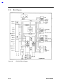
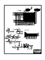
Figure 1-12
System Introduction
AMP
LM4836
AUD BD
Conn.
AUDIO
YMF715
Serial
Port
ISA Bus
ALI
M1533
Internal
AUD BD
FDD Conn.
Conn.
Super I/O
SMC
FDC 37C672
USB
Conn.
FIR
control
BIOS
ROM
Battery
Conn.
SMB Bus
KBC
M38813
VGA
C&T
65555
Charger
Conn.
System
CD-ROM
& HDDD
Conn.
DIMM2 Socket
DIMM1 Socket
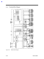
1.6.1
PCI Bus
ALI
M1531
Block Diagrams
PCMCIA
TI
PCI1250A
Cache
Tag Ram
CPU Bus
CPU P55C
1.6
System Block Diagram
1-31
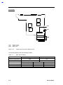
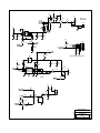
Figure 1-13
1-32
SGRAM CLK
DIMM2
DIMM1
72
38813
MODEM
37C672
YMF715
65555
48MHZ
65555
PCI1250
1533
1531
1533
USB
M1531
CACHE
CPU
14.318M
CPU CLK
PCI CLK
DIMM2
SMB BUS
DIMM1
CLK GEN
CY2272
M1533
1.6.2
Clock
Clock Block Diagram
Service Guide
1.7
Environmental Requirements
Table 1- 38
Environmental Requirements
Item
Specification
Temperature
Operating (ºC)
+5~ +35
Non-operating(ºC)
-20 ~ +60
Humidity
Operating (non-condensing)
20% ~ 80%
Non-operating (non-condensing)
20% ~ 80%
Operating Vibration (unpacked)
Operating
5 - 25.6Hz, 0.38mm; 25.6 - 250Hz, 0.5G
Sweep rate
0.5 octave / minute
Number of test cycles
2 / axis (X,Y,Z)
Non-operating Vibration (unpacked)
Non-operating
5 - 27.1Hz, 0.6G; 27.1 - 50Hz, 0.41mm; 50-500Hz, 2G
Sweep rate
0.5 octave / minute
Number of text cycles
4 / axis (X,Y,Z)
Non-operating Vibration (packed)
Non-operating
5 - 62.6Hz, 0.51mm; 62.6-500Hz, 4G
Sweep rate
0.5 octave / minute
Number of text cycles
4 / axis (X,Y,Z)
Shock
Operating
5G peak, 11±1ms, half-sine
Non-operating (unpacked)
40G peak, 11±1ms, half-sine
Non-operating (packed)
50G peak, 11±1ms, half-sine
Altitude
Operating
10,000 feet (5°C ~ 40°C)
Non-operating
40,000 feet (-10°C ~ 60°C)
ESD
Air discharge
8kV (no error)
12.5kV (no restart error)
15kV (no damage)
Contact discharge
4kV (no error)
6kV (no restart error)
8kV (no damage)
System Introduction
1-33
1.8
Mechanical Specifications
Table 1-39
Mechanical Specifications
Item
Specification
Weight
FDD model
CD-ROM model
(includes battery)
2.77 kg. (6.11 lb.)
2.8 kg. (6.2 lb.)
Dimensions
(main footprint)
WxDxH
311.5mm x 236/246mm x 46.5mm (12.26” x 9.29”/9.69” x 1.83”)
1-34
Service Guide
C h a p t e r
2
Major Chips Description
This chapter discusses the major chips used in the notebook.
Table 2-1
Major Chips List
Component
Vendor
Description
PCI 1250A
TI
PC Card controller chip
Aladdin IV (M1531/M1533)
ALi
System Architecture chipset
FDC37C672
SMC
Super I/O controller chip
65555
C&T
Video controller chip
M38813
YMF715B-S
Major Chips Description
Keyboard controller chip
Yamaha
Audio chip
2-1
2.1
PCI 1250A
The Texas Instruments PCI1250A is a high-performance PC Card controller with a 32-bit PCI
interface. The device supports two independent PC Card sockets compliant with the 1995 PC Card
Standard. The PCI1250A provides a rich featured set which make it the best choice for bridging
between PCI and PC Cards in both notebook and desktop computers. The 1995 PC Card Standard
retains the 16-bit PC Card specification defined in PCMCIA Release 2.1, and defines the new
32-bit PC Card, CardBus, capable of full 32-bit data transfers at 33 MHz. The PCI1250A supports
any combination of 16-bit and CardBus PC Cards in the two sockets, powered at 5V or 3.3V as
required.
The PCI1250A is compliant with the PCI Local Bus Specification Revision 2.1, and its PCI
interface can act as either a PCI master device or a PCI slave device. The PCI bus mastering is
initiated during 16-bit PC Card DMA transfers, or CardBus PC Card bridging transactions.
All card signals are internally buffered to allow hot insertion and removal without external
buffering. The PCI1250A is register compatible with the Intel 82365SL-DF ExCA controller. The
PCI1250A internal data-path logic allows the host to access 8-, 16-, and 32-bit cards using full
32-bit PCI cycles for maximum performance. Independent buffering and a pipeline architecture
provide an unsurpassed performance level with sustained bursting. The PCI 1250A can also be
programmed to accept fast posted writes to improve system-bus utilization.
The PCl1250A provides an internally buffered zoom video path. This reduces the design effort of
PC board manufacturers to add a ZV compatible solution and guarantees compliance with the
CardBus loading specifications. Multiple system interrupt signaling options are provided including:
parallel PCI, parallel ISA, serialized ISA, and serialized PCI. Furthermore, general purpose inputs
and outputs are provided for the board designer to implement sideband functions. Many other
features are designed into the PCI1250A such as socket activity LED outputs, and are discussed in
detail throughout the design specification.
An advanced CMOS process is used to achieve low system power consumption while operating at
PCI clock rates up to 33MHz. Several low-power modes allow the host power management system
to further reduce power consumption.
2.1.1
Features
•
PCI Power Management Compliant
•
ACPI 1.0 Compliant
•
Packaged in a 256-pin BGA
•
PCI Local Bus Specification Rev. 2.1 Compliant
•
1995 PC Card Standard Compliant
•
3.3 Volt Core Logic with Universal PCI Interfaces Compatible with 3.3 Volt and 5 Volt PCI
Signaling Environments
•
Mix and Match 5V/3.3V PC Card16 Cards and 3.3V CardBus Cards
•
Supports Two PC Card or CardBus Slots with Hot Insertion and Removal
•
Uses Serial Interface to TI TPS2206A Dual Power Switch
2-2
Service Guide
•
Supports Burst Transfers to Maximize Data Throughput on both PCI Buses
•
Supports Serialized IRQ with PCI Interrupts
•
8-Way Legacy IRQ Multiplexing
•
System Interrupts can be Programmed as PCI-style or ISA IRQ-style
•
ISA IRQ interrupts can be Serialized onto a single IRQSER pin
•
EEPROM Interface for Loading Subsystem ID and Subsystem Vendor ID
•
Pipelined Architecture allows Greater than 130 Mbytes per second throughput from CardBus
to PCI and from PCI to CardBus
•
Supports Zoom Video with Internal Buffering
•
Programmable Output Select for CLKRUN
•
Four General Purpose I/O's
•
Multi-function PCI Device with Separate Configuration Space for each Socket
•
Five PCI Memory Windows and Two l/O Windows Available to each PC Card16 Socket
•
Two I/O Windows and Two Memory Windows Available to each CardBus Socket
•
ExCA-Compatible Registers are Mapped in Memory and I/O Space
•
Supports Distributed DMA and PC/PCI DMA
•
Intel- 82365SL-DF Register Compatible
•
Support 16-bit DMA on both PC Card Sockets
•
Supports Ring indicate, SUSPEND, and PCI CLKRUN
•
Advanced Submicron, Low-Power CMOS Technology
•
Provides VGA / Palette Memory and I/O, and Subtractive Decoding Options
•
LED Activity Pins
•
Supports PCI Bus Lock
Major Chips Description
2-3
2.1.2
Block Diagram
A simplified block diagram of the PCI1250 is provided in following figure. The PCI interface
includes all address/data and control signals for PCI protocol. The interrupt interface includes
terminals for parallel PCI, parallel ISA, and serialized PCI & ISA signaling. The ring indicate
terminal is included in the interrupt interface, since it's function is to perform system wake-up on
incoming PC Card modem rings. Miscellaneous system interface terminals include GPIO signals,
PC/PCI DMA support signals, and socket activity LED signals.
Figure 2-1
2-4
PCI1250 Block Diagram
Service Guide
2.1.3
Terminal Functions
This section describes the PCI1250A terminal functions. The terminals are grouped in tables by
functionality such as PCI system function, power supply function, etc. for quick reference. The
terminal numbers are also listed for convenient reference.
Table 2-2
PCI1250 Terminal Functions
Name
No.
I/O Type
Function
Power Supply Terminals
GND
A01, D04, D08, D13,
17, H04, H17, N04,
N17, U04, U08, U13,
U17,
I
Device ground terminals
VCC
D06, D11, D15, F04,
F17, 04, L17, R04,
R17, U06, U10, U15
I
3.3 V Power supply terminal for core logic.
VCCA
K02, R03, W05
I
Rail Power Input for PC Card A Interface. Indicates
Card A signaling environment.
VCCB
B16, C10, F18
I
Rail Power Input for PC Card B Interface. Indicates
Card A signaling environment.
VCCI
V10
I
Rail power Input for interrupt subsystem interface
and miscellaneous l/O. Indicates signaling level of
the following inputs and shared outputs: IRQSER,
PCGNT. PCREQ SUSPENCX, SPKROUT,
GPI01:0, IRQMUX7:0, INTA, INTB CLOCK. DATA,
LATCH, and RI_OUT
VCCP
K20, P18, V15, W20
I
Rail power input for PCI signaling.
VCCZ
A04, D01
I
Rail power input for the Zoom Video Interface
PCI System Terminals
PCLK
J17
I
PCI bus clock. Provides timing fot all transactions
on the PCI bus. All PCI signals are sampled at the
rising edge H PCLK.
PRST
J19
I
PCI reset When the PCI bus reset is asserted the
PRST signal causes the PCI 1 250A to 3-state all
output buffers and reset all internal registers. When
PRST is asserted, the device is completely
nonfunctional. After PRST is deasserted, the
PCI1250A is in its default state.
When the SUSPEND mode is enabled, the device
is protected from the PRST clearing the internal
registers. An outputs are 3-statea but the contents
of the registers are preserved
CLKRUN
J18
Major Chips Description
O
PCI clock run. This signal is used by the central
resource to request permission to stop the PCI
clock or to slow it down, and the PCI1250A
responds accordingly.
2-5
Table 2-2
PCI1250 Terminal Functions
Name
No.
I/O Type
Function
PCI Address and Data Terminals
PCI address data bus. These signals make up the
multiplexed PCI address and data bus on the
primary interface. During the address phase of a
primary bus PCI cycle, AD31:0 contain a 32-bit
address or other destination. During the data
phase AD31 0 contain data.
AD31
AD30
AD29
AD28
AD27
AD26
AD25
AD24
AD23
AD22
AD21
AD20
AD19
AD18
AD17
AD16
AD15
AD14
AD13
AD12
AD11
AD10
AD9
AD8
AD7
AD6
AD5
AD4
AD3
AD2
AD1
AD0
K18
K19
L20
L18
L19
M20
M19
M18
N19
N18
P20
P19
R20
R19
P17
R18
V18
Y19
W18
V17
U16
Y18
W17
V16
W16
U14
Y16
W15
V14
Y15
W14
Y14
C/BE3
C/BE2
C/BE1
C/BE0
M17
T20
W19
Y17
I/O
PCI bus commands and byte enables. These
signals are multiplexed on the same PCI terminals.
During address phase of a primary bus PCI cycle,
C/BE3:0 define the bus command. During the data
phase, this four-bit bus is used as byte enables.
The byte enables determine which byte paths of the
full 32-bit data bus carry meaningful data. C/BE0
applies to byte 0 (AD7:0), C/BE1 applies to byte 1
(AD15:8), C/be2 applies to byte 2 (AD23:16) and
C/BE3 applies to byte 3 (AD31:24).
PAR
Y20
I/O
PCI bus party In all PCI bus read and write cycles
the PCI1250A calculates even parity across the
AD31:0 and C/BE3:0 buses. As an initiator during
PCI cycles, the PCI1250A outputs this parity
indicator with a one PCLK delay. As a target during
PCI cycles. the calculated parity is compared to the
initiators parity indicator. A miscompare can result
in the assertion of a parity error (PERR).
2-6
Service Guide
Table 2-2
PCI1250 Terminal Functions
Name
No.
I/O Type
Function
PCI Interface Control Terminals
DEVSE
V20
I/O
PCI device select. The PCI1250A asserts this signal
to claim a PCI cycle as the target device. As a PCI
initiator on the bus. the PCI1250A monitors this
signal until a target responds. If no target responds
before time-out occurs, then the PCI1250A will
terminate the cycle with an initiator abort.
FRAME
T19
I/O
PCI cycle frame. This signal is driven by the
initiator of a bus cycle. FRAME is asserted to
indicate that a bus transaction is beginning, and
data transfers continue while this signal is asserted.
When FRAME is deasseerted the PCI bus
transaction is in the final data phase.
GNT
J20
I
PCI bus grant. This signal is driven by the PCI bus
arbiter to grant the PCI1250A access to the PCI bus
after current data transaction has completed. This
signal may or may not follow a PCI bus request
depending upon the PCI bus parking algorithm.
GPIO2/LOCK
V19
I/O
PCI bus general purpose l/O pins or PCI bus lock.
These pins are can be configured as PCI LOCK and
used to gain exclusive access downstream. Since
this functionality is not typically used, a general
purpose I/O may be accessed through this terminal.
This terminal defaults to a general purpose input,
and maybe configured through the GPIO2 Control
Register
IDSEL
N20
I
Initalization device select. IDSEL selects the
PCI1250A during configuration space accesses.
IDSEL can be connected to one of the upper 24 PCI
address lines on the PCI bus.
IRDY
T18
I/O
PCI initiator ready. IRDY indicates the PCI bus
initiator’s ability to complete the current data phase
of the transaction. A data phase is completed upon
a rising edge of PCLK where both IRDY and TRDY
are asserted. Until IRDY and TRDY are both
sampled asserted. wait states are inserted.
PERR
U18
I/O
PCI parity error indicator. This signal is driven by a
PCI device to indicate that calculated parity does
not match PAR, when PERR is enabled through bit
6 of the command register.
REQ
K17
O
PCI bus request. Asserted by the PCI1250A to
request access to the PCI bus as an initiator.
SERR
U19
O
PCI system error. Output that is pulsed from the
PCI1250A, when enabled through the command
register, indicating a system error has occurred.
The PCI 1250A needs not be the target of the PCI
cycle in order to assert this signal. When SERR is
enabled in the control register, this signal will also
pulse indicating that address parity error has
occurred on a CardBus interface.
Major Chips Description
2-7
Table 2-2
PCI1250 Terminal Functions
Name
No.
I/O Type
Function
STOP
T17
I/O
PCI cycle stop signal. This signal is driven by a PCI
target to request the initiator to stop the current PCI
bus tranaction. This signal is used for target
disconnects and is commonly asserted by target
devices which do not support burst data transfers.
TRDY
U20
I/O
PCI target ready. TRDY indicates the primary bus
target s ability to complete the current data phase
of the transaction. A data phase is completed upon
a rising edge of PCLK where both IRDY and TRDY
are asserted. Until both IRDY and TRDY are
asserted, wait states are inserted.
PC Card 16 Address And Data Terminals (Slot A And Slot B)
A25
A24
A23
A22
A21
A20
A19
A18
A17
A16
A15
A14
A13
A12
A11
A10
A9
A8
A7
A6
A5
A4
A3
A2
A1
A0
Slot A1
Slot B2
T04
U02
U01
P04
R02
R01
P01
N02
M04
T01
T02
P02
N03
T03
M01
L01
M03
N01
V01
V02
V03
W02
W03
W04
V04
U05
C14
B15
C15
C16
A18
C17
B18
A20
C18
A17
A16
B17
A19
D14
D18
E18
B20
B19
A15
A14
B13
A13
C12
A12
B11
C11
O
PC Card Address 16-bit PC Card address lines.
A25 is the most significant bit
1
Terminal name for slot A is preceded with A_. For example, the full name for terminal T04 is A_A25.
2
Terminal name for slot B s preceded with B_. For example, the full name for terminal C14 is B_A25.
2-8
Service Guide
Table 2-2
PCI1250 Terminal Functions
Name
D15
D14
D13
D12
D11
D10
D9
D8
D7
D6
D5
D4
D3
D2
D1
D0
No.
K03
J02
J04
H02
G01
W08
Y07
V07
J01
J03
H01
H03
G02
V08
W07
Y06
E19
E20
G18
G19
H18
B07
C08
A08
G17
F19
F20
F19
H19
A07
B08
D09
I/O Type
I/O
Function
Card Data. 16-bit PC Card data lines. D15 is the
most significant
16-Bit PC Card Interface Control Terminals (Slot A And Slot B)
BVD1
(STSCHG/RI)
Slot A3
Slot B4
V06
A09
Battery Voltage Detect 1. Generated by 16-bit
memory PC Cards that include batteries. BVD1 is
used with BVD2 as an indication of the condition of
the batteries on a memory PC Card. Both BVD1
and BVD2 are kept high when the battery is good.
When BVD2 is low and BVD1 is high, the battery is
weak and needs to be replaced. When BVD1 is
low, the battery is no longer serviceable and the
data in the memory PC Card is lost. See the Card
Status Change interrupt Configuration register for
enable bits. See the Card Status Change register
and the Interface Status register for the status bits
for this signal.
Status Change (STSCHG). STSCHG is used to
alert the system to a change in the READY, write
protect, or battery voltage dead condition of a 16bit l/O PC Card.
Ring Indicate (RI). Ring indicate is used by 16-bit
modem cards to indicate a ring detection.
3
Terminal name for slot A is preceded with A_. For example, the full name for terminal W01 is A_ESET
4
Terminal name for slot B s preceded with B_. For example, the full name for terminal B13 is B_RESET
Major Chips Description
2-9
Table 2-2
PCI1250 Terminal Functions
Name
BVD2
(SPKR)
No.
Y05
D10
I/O Type
I
Function
Battery Voltage Detect 2. Generated by 16-bit
memory PC Cards that include batteries. BVD2 is
used with BVD1 as an indication of the condition of
the batteries on a memory PC Card. Both BVD1
and BVD2 are high when the battery is good. When
BVD2 is low and BVD1 is high, the battery is weak
and needs to be replaced. When BVD1 is low, the
battery is no longer serviceable and the data in the
memory PC Card is lost. See the Card Status
Change Interrupt Configuration Register for enable
bits. See the Card Status Change register and the
Interface Status register for the status bits for this
signal.
Speaker (SPKR) Speaker is an optional binary
audio signal available only when the card and
socket have been configured: for the 16-bit l/O
interface. The audio signals from cards A and B are
combined by the PCI 1250A and are output on the
SPKROUT pin.
DMA Request.: This pin may be used as the DMA
request signal during DMA operations to a 16-bit
PC Card that supports DMA. The PC Card asserts
this signal to indicate a request for a DMA
operation.
CD1
CD2
G03
W06
H20
C09
I
PC Card Detect 1 and Card Detect 2. CD1 and CD2
are connected to ground internally on the PC Card.
When a PC Card is inserted into a socket. these
signals are pulled low. The signal status is available
by reading the interface status register
CE1
CE2
K01
L02
D20
D19
O
Card Enable 1 and Card Enable 2. These signals
enable even and odd numbered address bytes. CE1
enables even numbered address bytes and CE2
enables odd numbered address bytes.
INPACK
Y01
D12
I
Input acknowledge. This signal is asserted by the
PC Card when it can respond to an l/O read cycle
at the current address.
DMA Request. This pin may be used as the DMA
request signal during DMA operations from a 16-bit
PC Card that supports DMA. If used as a strobe,
the PC Card asserts this signal to indicate a
request for a DMA operation.
IORD
L04
E17
O
I/O read. IORD is asserted by the PCI1250A to
enable 16-bit t/O PC Card data output during host
l/O read cycles.
DMA Write. This pin is used as the DMA write
strobe during DMA operations from a 16-bit PC
Card which supports DMA. The PCI1250A asserts
this signal during DMA transfers from the PC
Card to host memory.
2-10
Service Guide
Table 2-2
PCI1250 Terminal Functions
Name
IOWR
No.
M02
C19
I/O Type
O
Function
I/O Write IOWR is driven low by the PCI1250A to
strobe write data into 16-bit l/O PC Cards during
host l/O write cycles.
DMA Read. This pin is used as the DMA write
strobe during DMA operations from a 16-bit PC
Card that supports DMA. The PCI1250A asserts
this signal during transfers from host memory to
the PC Card.
OE
L03
C20
O
Output Enable. OE is driven low by the PCl1250A
to enable 16-bit Memory PC Card data output
during host memory read cycles.
DMA terminal count. This pin is used as TC during
DMA operations to a 16-bit PC Card which supports
DMA. The PCI1250A asserts this signal to indicate
terminal count for a DMA write operation
READY/IREQ
Y04
A10
I
The ready function is provided by the READY signal
when the 16-bit PC Card and the host socket are
configured for the memory-only interface. READY
is driven low by the 16-bit Memory PC Cards to
indicate that the memory card circuits are busy
processing a previous write command. READY is
driven high when the 16-bit Memory PC Card is
ready to accept a new data transfer command.
Interrupt Request. IREQ is asserted by a 16-bit l/O
PC Card to indicate to the host that a device on the
16-bit l/O PC Card requires service by the host
software. IREQ is high (deasserted) when no
interrupt is requested.
REG
Y02
B12
O
Attribute memory select. REG remains high for all
common memory accesses. When REG is asserted
access is limited to attribute memory (OE or WE
active) and to 1he l/O space (IORD or IOWR
active}. Attribute memory is a separately accessed
section of card memory and is generally use to
record card capacity and other configuration and
attribute information.
DMA acknowledge. This pin is used as a DACK
during DMA operations to a 16-bit PC Card that
supports DMA. The PCI1250A asserts this signal to
indicate a DMA operation. This signal is used in
conjunction with the DMA read (IOWR) or DMA
write (IORD) strobes to transfer data.
RESET
W01
C13
O
PC Card reset. RESET forces a hard reset to a 16bit PC Card
WAIT
V05
B10
I
Bus cycle wait. WAIT is driven by a 16-bit PC Card
to delay the completion of (i.e.. extend) the memory
or l/O cycle that is in progress.
Major Chips Description
2-11
Table 2-2
PCI1250 Terminal Functions
Name
WE
No.
P03
D16
I/O Type
O
Function
Write enable. WE is used to strobe memory write
data into 16-bit memory PC Cards. WE is also use
for memory PC Cards that employ programmable
memory technologies.
DMA terminal count. This pin is used as TC during
DMA operations to a 16-bit PC Card which supports
DMA. The PC1031 asserts this signal to indicate
terminal count for a DMA read operation.
WP
(IOIS16)
U07
B09
I
Write protect. This signal applies to 16-bit memory
PC Cards. WP reflects the status of the writeprotect switch on 16-bit memory PC Cards. For 16bit l/O cards, WP is used for the 16-bit port
(IOSI16) function.
IOIS16 (I/O is 16-bits). This signal applies to 16-bit
l/O PC Cards. IOIS16 is asserted by the 16-bit PC
Card when the address on the bus corresponds to
an address to which the 16-bit PC Card responds
and the l/O port that is addressed is capable of 16bit accesses.
DMA request. This pin can be used as the DMA
request signal during DMA operations to a 16-bit
PC Card which supports DMA. If used, the PC Card
asserts this signal to indicate a request for a DMA
operation
VS1
VS2
Y03
U03
A11
B14
I/O
Voltage Sense 1 and Voltage Sense 2. VS1 and
VS2, when used in conjunction with each other,
determine the operating voltage of the 16-bit PC
Card.
Cardbus PC Card Interface System Terminals
CCLK
Slot A5
Slot B6
T01
A17
O
CardBus PC Card Clock. This signal provides
synchronous timing for all transactions on the ]
CardBus interface. All signals except CRST,
CCLKRUN, CINT, CSTSCHG. CAUDIO, CCD2:1,
and CVS2.1 are sampled on the rising edge of the
CCLK, and all timing parameters are defined with
the rising edge of this signal. The CardBus clock
operates at the PCI bus clock frequency, but it can
be stopped in the low state or slowed down for
power savings.
5
Terminal name for slot A is preceded with A_. For example, the full name for terminal N03 is A_CPAR.
6
Terminal name for slot B s preceded with B_. For example, the full name for terminal A19 is B_CPAR.
2-12
Service Guide
Table 2-2
PCI1250 Terminal Functions
Name
No.
I/O Type
Function
CRSST
W01
C13
I/O
CardBus PC Card Reset. This signal is used to
bring CardBus PC Card specific registers,
sequencers, and signals to a known state. When
CRST is asserted, all CardBus PC Card signals
must be 3-statedt and the PCI1250A will drive
these signals to a valid logic level. Assertion may
be asynchronous to the CCLK. But deassertion
must be synchronous to the CCLK.
CCLKRUN
U07
B09
O
CardBus PC Card Clock Run. This signal is used
by a CardBus PC Card to request an increase in
the CCLK frequency. and the PCI 1 250A to
indicate that the CCLK frequency will be decreased.
CardBus PC Card Address and Data Terminals (Slot A and Slot B)
CAD31
CAD30
CAD29
CAD28
CAD27
CAD26
CAD25
CAD24
CAD23
CAD22
C AD21
CAD20
CAD19
CAD18
CAD17
CAD16
CAD15
CAD14
CAD13
CAD12
CAD11
CAD10
CAD9
CAD8
CAD7
CAD6
CAD5
CAD4
CAD3
CAD2
CAD1
CAD0
W08
Y07
W07
V07
Y06
U05
V04
W04
W03
W02
V03
V02
T04
V01
U02
M04
M02
M03
L04
M01
L03
L02
L01
K03
J01
J04
J03
H02
H01
G01
H03
G02
Major Chips Description
B07
C08
B08
A08
D09
C11
B11
A12
C12
A13
B13
A14
C14
A15
B15
C18
C19
B20
E17
D18
C20
D19
E18
E19
G17
G18
F19
G19
F20
H18
G20
H19
I/O
PC Card Address and Data bus. These signals
make up the multiplexed CardBus address and data
bus on the CardBus interface. During the address
phase of a CardBus cycle, CAD31:0 contain a 32bit address. During the data phase of a CardBus
cycle, CAD31:0 contain data. CAD31 is the most
significant bit
2-13
Table 2-2
PCI1250 Terminal Functions
Name
No.
I/O Type
Function
CC/BE3
CC/BE2
CC/BE1
CC/BE0
Y02
T03
N01
K01
B12
D14
B19
D20
I/O
CardBus Bus Commands and Byte Enables. The
command and byte enable signals are multiplexed
on the same CardBus terminals. During the
address phase of a CardBus cycle, CC/BE3:0
defines the bus command. During the data phase,
this four-bit bus is used as byte enables. The byte
enables determine which byte paths of the full 32bit data bus carry meaningful data. CC/BE0 applies
to byte 0 (CAD7:0), CC/BE1 applies to byte 1
(CAD15:8), CC/BE2 applies to byte 2 (CAD23:8),
and CC/BE3 applies to byte 4(CAD31:24)
CPAR
N03
A19
I/O
CardBus Parity. In all CardBus read and write
cycles, the PCl1250A calculates even parity cross
the CAD and CC/BE buses. As an initiator during
CardBus cycles, the PC11250A outputs this parity
indicator with a one CCLK delay. As a target
during CardBus cycles, the calculated parity is
compared to the initiator's parity indicator; a
miscompare can result in a parity error assertion.
Cardbus Interface Control Terminals
Slot A
Slot B
CAUDIO
Y05
D10
I
CardBus Audio. This signal is a digital input signal
from a PC Card to the system speaker. The
PCI1250A supports the binary audio mode, and
outputs a binary signal from the card to the
SPKROUT signal
CBLOCK
P01
B18
I/O
CardBus Lock. This signal is used to gain exclusive
access to a target
CCD1
CCD2
G03
W06
H20
C09
I
CardBus Detect 1 and CardBus Detect 2. These
signals are used in conjunction with voltage sense
signals to identify ca d insertion and interrogate
cards to determine the operating voltage and card
type.
CDEVSEL
R02
A18
I/O
CardBus device select. The PCI1250A asserts this
signal to claim a CardBus cycle as the target
device. As a CardBus initiator on the bus, the
PCI1250A monitors this signal until a target
responds. If no target responds before time-out
occurs, then the PCI1250A will terminate the cycle
with an initiator abort.
CFRAME
U01
C15
I/O
CardBus cycle frame. This signal is driven by the
initiator of a CardBus bus cycle. CFRAME is
asserted to indicate that a bus transaction is
beginning. and data transfers continue while this
signal is asserted. When CFRAME is deasserted
the CardBus bus transaction is in the final data
phase.
CGNT
P03
D16
I
CardBus bus grant. This signal is driven by the
PCI1250A to grant a CardBus PC Card access to
the CardBus bus after ihe current data transaction
has completed.
2-14
Service Guide
Table 2-2
PCI1250 Terminal Functions
Name
No.
I/O Type
Function
CINT
Y04
A10
I
CardBus interrupt. This signal is asserted low by a
CardBus PC Card to request interrupt servicing
from the host.
CIRDY
T02
A16
I/O
CardBus initiator ready. CIRDY indicates the
CardBus initiator's ability to complete the current
data phase of the transaction. A data phase is
completed upon a rising edge of CCLK where both
CIRDY and CTRDY are asserted. Until CIRDY and
CTRDY are both sampled asserted, wait states are
inserted.
CPERR
P02
B17
I/O
CardBus Parity Error. This signal is used to report
parity errors during CardBus transactions, except
during special cycles. It is driven low by a target
two clocks following that data when a parity error is
detected.
CREQ
Y01
D12
I
CardBus Request. This signal indicates to the
arbiter that the CardBus PC Card desires use of the
CardBus bus as an initiator
CSERR
V05
B10
I
CardBus System Error. This signal reports address
parity errors and other system errors which could
lead to catastrophic results. CSERR is driven by the
card synchronous to CCLK but ceasserted by a
weak pull-up, and may take a few CCLK periods.
The PCI1250A can report CSERR to the system by
assertion of SERR on the PCI interface.
CSTOP
R01
C17
I/O
CardBus Stop Signal. This signal is driven by a
CardBus target to request the initiator to stop the
current CardBus transaction. This signal is used for
target disconnects, and is commonly asserted by
target devices which do not support burst data
transfers.
CSTSCHG
V06
A09
I
CardBus Status Change. CSTSCHG is used to alert
the system to a change in the card's status, and is
used as a wake-up mechanism.
CTRDY
P04
C16
I/O
CardBus Target Ready. CTRDY indicates the
CardBus target's ability to complete the current
data phase of the transaction. A data phase is
completed upon a rising edge of CCLK where both
CIRDY and CTRDY are asserted; until which wait
states are inserted
CVS1
CVS2
Y03
U03
A11
B14
I/O
CardBus Voltage Sense 1 and Voltage Sense 2.
These signals are used in conjunction with card
detect signals to identify card insertion and
interrogate cards to determine the operating voltage
and card type.
Major Chips Description
2-15
Table 2-2
PCI1250 Terminal Functions
Name
No.
I/O Type
Function
System Interrupt Terminals
GPIO3/INTA
V13
I/O
GPI03/lNTA Parallel PCI Interrupt. This terminal
can be connected to an available PCI interrupt if
parallel PCI interrupts are used, and the PCI1250A
will output PCI INTA through this terminal. Refer to
the Interrupt Subsystem description in this
document for details on interrupt signaling. This
terminal defaults to a general purpose input
IRQSER/INTB
W13
I/O
IRQSER Serial Interrupt Signal / INTB Parallel PCI
Interrupt. When this terminal is configured as
IRQSER, it provides the IRQSER style serial
interrupting scheme. Serialized PCI interrupts can
also be sent in the IRQSER stream. This terminals
can be configured as the parallel PCI INTB
interrupt. Refer to the Interrupt Subsystem
description in this document for details on interrupt
signaling. This terminal defaults to the IRQSER
signal since this is the default interrupt signaling
method
IRQMUX7
IRQMUX6
IRQMUX5
IRQMUX4
IRQMUX3
IRQMUX2
IRQMUX1
IRQMUX0
Y12
U11
W10
Y09
W09
V09
U09
Y08
O
The primary function of these terminals is to
provide the ISA type IRQ signaling supported by the
PCl1250A. These Interrupt mux outputs can be
mapped to any of 15 IRQs. The Device Control
register must be programmed for the ISA IRQ
interrupt mode and the IRQMUX Routing Register
must have the IRQ routing programmed before
these terminals are enabled.
All of these terminals have secondary functions,
such as PC/PCI DMA request/grant, ring indicate
output, and zoom video status. that can be
selected; with the appropriate programming of this
register. When the secondary functions are
enabled, the respective terminals are not available
for IRQ routing.
See the IRQMUX Routing register for programming
options
RI-OUT/PME
Y13
O
Ring indicate Output/Power Management Event.
RI_OUT allows the RI input from one of the PC
Cards to pass through o the system. This pin is the
RI_OUT signal when the PCI1250A is in the D0
(fully on) state and provides the PME signal when
the device is in a D1, D2, or D3 state.
IRQMUX4 or IRQMUX3 can be used to route the
RI_OUT signal when the PME signal is routed on
pin Y13 and a PC Card requires a ring indicate
signal
PC Card Power Switch Terminals
LATCH
2-16
W13
O
3-Line power Switch latch. This signal is asserted
by the PCI1250A to indicate to the PC Card power
switch that the data on the DATA line is valid.
Service Guide
Table 2-2
PCI1250 Terminal Functions
Name
CLOCK
No.
U12
I/O Type
I/O
Function
3-Line Power Switch Clock. Information on the
DATA line is sampled at the rising edge of CLOCK.
This terminal defaults to an input, but can be
changed to a PCI1250A output by using the
P2CCLK bit in the I/O System Control Register. The
TPS2206 defines the maximum frequency of this
signal to be 2MHz.
If a system design defines this terminal an output,
then this terminal requires an external pull-up
resister. The frequency of the PCI1250A output
CLOCK is derived from dividing the PCI CLK by 36
DATA
V12
O
3-Line Power Switch Data. This signal is used to
serially communicate socket power control
information to the power switch.
Zoomed Video Terminals
I/O and
Memory
Interface
Signal
ZV_HREF
A06
A10
O
Horizontal Sync to the zoom video port.
ZV_VSYNC
C07
A11
O
Vertical sync to the zoom video port.
ZV_Y7
ZV_Y6
ZV_Y5
ZV_Y4
ZV_Y3
ZV_Y2
ZV_Y1
ZV_Y0
A03
B04
C05
B05
C06
D07
A05
B06
A20
A14
A19
A13
A18
A8
A17
A9
O
Video data to the zoom video port in YV:4:2:2
format.
D02
C03
B01
B02
A02
C04
B03
D05
D02
C03
B01
B02
A02
C04
B03
D05
A25
A12
A24
A15
A23
A16
A22
A21
O
Video data to the zoom video port in YV:4:2:2
format.
ZV_SCLK
C02
A7
O
Audio SCLK PCM signal.
ZV_MCLK
D03
A6
O
Audio MCLK PCM signal.
ZV_PCLK
E01
IOIS16
O
Pixel clock (PCLK) to the zoom video port.
ZV_LRCLK
E03
INPACK
O
Audio LRCLK PCM signal.
ZV_SDATA
E02
SPKR
O
Audio PCM data signal (SDATA)
ZV_RSVD
F1
F2
F3
G4
O
Reserved. No connection.
ZV_RSV1
ZV_RSV0
C1
E4
O
Reserved. No connection in PC Card. These
signals are put into a high-impedance state by the
host adapter.
Major Chips Description
A5
A4
2-17
Table 2-2
PCI1250 Terminal Functions
Name
No.
I/O Type
Function
PC/PCI DMA Terminals
PCREQ/
IRQMUX7
Y12
O
PC/PCI DMA Request. This signal is used to
request DMA transfers as DREQ in a system
supporting the PC. PCI DMA scheme.
IRQMUX7. When this terminal is configured for
IRQMUX7, it provides the IRQMUX7 interrupt
output of the interrupt mux, and can be mapped to
any of 15 ISA type IRQs. The IRQMUX7 signal
takes precedence over PCREQ, and should not be
enabled in a system using PC/PCI DMA.
This pin is also used for the serial EEPROM
interface.
PCGNT/
IRQMUX6
U11
I/O
PC/PCI DMA Grant. This signal is used to grant the
DMA channel to a requester in a system supporting
the pr PCI DMA scheme.
IRQMUX6. When :his terminal is configured for
IRQMUX6, it provides the IRQMUX6 interrupt
output of the interrupt mux, and can be mapped to
any of 15 ISA type IRQs. The IRQMUX6 signal
takes precedence over PCGNT, and should not be
enabled in a system using PC/PCI DMA.
This pin is also used for the serial EEPROM
interface.
Miscellaneous Terminals
GPIO0/
LEDA1
V11
I/O
GPIO0 / Socket Activity LED Indicator 1. When this
signal is configured as LEDA1 it provides an output
indicating PC Card socket O activity. Otherwise,
this signal can be configured as a general purpose
input and output, GPIO0. The zoom video enable
signal (ZVSTAT) can also be routed to this signal
through the GPIO0 Control register. This terminal
defaults to a general purpose input.
GPIO1/
LEDA2
W11
I/O
GPI01 / Socket Activity LED Indicator 2. When this
signal is configured as LEDA2 it provides an output
indicating PC Card socket 1 activity. Otherwise, this
signal can be configured as a general purpose input
and output. GPIO1. A CSC interrupt can be
generated on a GPDATA change, and this input can
be used for power switch overcurrent (OC) sensing.
Refer to the GPI01 Control resister for
programming details. This terminal defaults to a
general purpose input.
SUSPEND
Y1
I
Suspend. This signal is used to protect the internal
registers from clearing when the PRST signal is
asserted. For details on implementing SUSPEND in
your system power management scheme refer to
the section on SUSPEND mode.
2-18
Service Guide
Table 2-2
PCI1250 Terminal Functions
Name
SPKROUT
No.
Y10
Major Chips Description
I/O Type
O
Function
Speaker Output. This signal is the output to the
host system that can carry the SPKR or CAUDIO
signal through the PCI1250A from the PC Card
interface. This signal is driven as the exclusive OR
combination of card SPKR//CAUDIO inputs.
2-19
2.2
Aladdin IV (M1531/M1533)
The Aladdin-IV is the succeeding generation chipset of Aladdin-III from Acer Labs. It maintains the
best system architecture (two-chip solution) to achieve the best system performance with the
lowest system cost (TTL-free). The Aladdin-IV consists of two BGA chips to give the 586-class
system a complete solution with most up-to-date features and architecture for multimedia/
multithreading OS and software applications. It utilizes the modern BGA package to improve the
AC characterization, resolves system bottleneck and makes the system manufacturing easier.
2.2.1
M1531
The M1531 includes:
•
Higher CPU bus frequency (up to 83.3 MHz) interface for the incoming Cyrix M2 and AMD K6,
PBSRAM and Memory Cache L2 controller
•
Internal MESI tag bits (8K x 2) to reduce cost and enhance performance
•
High-performance FPM/EDO/SDRAM DRAM controller
•
PCI 2.1 compliant bus interface
•
•
•
Smart deep buffer design for CPU-to-DRAM, CPU-to-PCI, and PCI-to-DRAM to achieve the
best system performance
Highly efficient PCI fair arbiter
The most flexible 32/64-bit memory bus interface for the best DRAM upgrade ability and
ECC/parity design to enhance the system reliability
With the concurrent bus design, PCI-to-PCI access can run concurrently with CPU-to-L2 and CPUto-DRAM access, while PCI-to-DRAM access can run concurrently with CPU-to-L2 access. The
M1531 also supports the snoop ahead feature to achieve the PCI master full-bandwidth access
(133 MB) and provides the enhanced power management features including ACPI support,
suspend DRAM refresh, and internal chip power control to support the Microsoft’s On Now
technology OS.
The M1533 offers the best power management system solution. It integrates ACPI support, deep
green function, two-channel dedicated Ultra-33 IDE master controller, two-port USB controller,
SMBus controller, and PS2 keyboard/mouse controller.
The M1543 provides the best desktop system solution. It integrates ACPI support, green function,
two-channel dedicated Ultra-33 IDE Master controller, two-port USB controller, SMBus controller,
PS/2 keyboard/mouse controller and the Super I/O (Floppy Disk Controller, two serial port/one
parallel port) support.
The Aladdin-IV gives a highly-integrated system solution and a most up-to-date architecture to
provide the best cost/performance system solution for desktop and notebook vendors.
2-20
Service Guide
2.2.1.1
•
•
Features
Supports all Intel/Cyrix/AMD/TI/IBM 586 processors. Host bus at 83.3, 75, 66, 60 and 50 MHz
at 3.3V/2.5V
Supports Linear Wrap mode for Cyrix M1 and M2
• Write-Allocation feature for K6
• Pseudo-Synchronous PCI bus access
(CPU bus: 75 MHz - PCI bus: 30 MHz, CPU bus: 83.3 MHz - PCI bus: 33 MHz)
•
Supports Pipelined-burst SRAM/Memory Cache
• Direct mapped, 256 KB/512 KB/1 MB
• Write-Back/Dynamic-Write-Back cache policy
• Built-in 8K x 2 bit SRAM for MESI protocol to reduce cost and enhance performance
• Cacheable memory up to 64 MB with 8-bit Tag SRAM
• Cacheable memory up to 512 MB with 11-bit Tag SRAM
• 3-1-1-1-1-1-1-1 for Pipelined-burst SRAM/Memory Cache at back-to-back burst read and
write cycles
• 3.3V/5V SRAMs for Tag address
• CPU single-read cycle L2 allocation
•
Supports FPM/EDO/SDRAM DRAMs
• 8 RAS lines up to 1 GB support
• 64-bit data path to memory
• Symmetrical/Asymmetrical DRAMs
• 3.3V or 5V DRAMs
• Duplicated MA[1:0] driving pins for burst access
• No buffer needed for RASJ and CASJ and MA[1:0]
• CBR and RAS-only refresh for FPM
• CBR and RAS-only refresh and Extended refresh and self refresh for EDO
• CBR and Self refresh for SDRAM
• 16 Qword deep merging buffer for 3-1-1-1-1-1-1-1 posted-write cycle to enhance highspeed CPU burst access
• 6-3-3-3-3-3-3-3 for back-to-back FPM read page hit, 5-2-2-2-2-2-2-2 for back-to-back EDO
read page hit, 6-1-1-1-2-1-1-1 for back-to-back SDRAM read page hit, 2-2-2-2 for retired
data for posted write on FPM and EDO page-hit, x-1-1-1 for retired data for posted write
SDRAM page-hit
• Enhanced DRAM page miss performance
• Supports 64 Mbit (16M x 4, 8M x 8, 4M x 16) technology of DRAMs
• Supports Programmable-strength RAS/CAS/ MWEJ/MA buffers
• Supports Error Checking and Correction (ECC) and Parity for DRAM
Major Chips Description
2-21
• Supports the most flexible six 32-bit populated banks of DRAM for easy DRAM upgrade
• Supports SIMM and DIMM
• Synchronous/Pseudo Synchronous 25/30/33MHz 3.3V/5V tolerance PCI interface
• Concurrent PCI architecture
• PCI bus arbiter: five PCI masters and M1533/ M1543 (ISA Bridge) supported
• 6 DWords for CPU-to-PCI memory write posted buffers
• Converts back-to-back CPU to PCI memory write to PCI burst cycle
• 38/22 Dwords for PCI-to-DRAM Write-posted/ Read-prefetching buffers
• PCI-to-DRAM up to 133 MB/sec bandwidth (even when L1/L2 write-back)
• L1/L2 pipelined-snoop ahead for PCI-to-DRAM cycle
• Supports PCI mechanism #1 only
• Complies with PCI spec. 2.1 (N(32/16/8)+8 rule, passive release, fair arbitration)
• Enhanced performance for Memory-Read-Line, Memory-Read-Multiple and Memory-writeInvalidate PCI commands
•
Enhanced Power Management
• ACPI support
• PCI bus CLKRUN function
• Dynamic Clock Stop
• Power-on Suspend
• Suspend to Disk
• Suspend to DRAM
• Self refresh during Suspend
•
2-22
328-pin (27mm x 27mm) BGA package
Service Guide
2.2.1.2
Pin Diagram
1
A
NC
2
3
PHLDAJ
4
AD3 AD6
5
6
7
AD8 AD12 PAR
8
TRDYJ
9
10
11
12
AD17 AD22 AD25 AD30 REQJ3
B BEJ0 PHLDJAD2 AD5
AD7 AD11 CBEJ1 DEVSELJ AD16 AD21 AD24
C BEJ3 BEJ2 BEJ1 AD4
CBEJ0
D BEJ6 BEJ5 BEJ4 AD0
AD1 AD9
AD14
LOCKJ FRAMEJ AD19 AD23
E DCJ
RSTJ
AD13
SERRJ IRDYJ AD18 PCLKIN AD26
F
HITMJ
EADSJ BEJ7
AD10 AD15
PCIMRQJ
13
STOPJ CBEJ2
AD29
CACHEJ AHOLD KENJ
15
16
GNTJ2 GNTJ3 MPD2 MPD0
AD20 CBEJ3 AD28 REQJ1
GNT0J MPD4
18
19
20
MD61 MD29 MD62
MD30 MD25 MD58 MD26 MD59
AD27 REQJ0 MPD7 MPD3 MD55 MD23 MD56 MD24 MD57
AD31
MPD6 MD31 MD20 MD53
VCC_C VCC_C MD50
M1531
NAJ VCC_A
17
REQJ2 GNTJ1 MPD5 MPD1 MD63 MD27 MD60 MD28
BRDYJ BOFFJ SMIACTJ HLOCKJ ADSJ VCC_B
G HD63
14
MD21 MD54
MD22
MD18 MD51 MD19 MD52
VCC_C MD15 MD48 MD16 MD49 MD17
H HD60 HD61 HD62 WRJ
MIOJ
GND GND
GND GND
GND GND
MD45 MD13 MD46 MD14 MD47
J
HD59
GND GND
GND GND
GND GND
MD10 MD43 MD11 MD44 MD12
K HD51 HD52 HD53 HD54 HCLKIN
GND GND
GND GND
GND GND
MD40 MD8
L
GND GND
GND GND
GND GND
MD5 MD38 MD6 MD39 MD7
HD55 HD56 HD57 HD58
HD46 HD47 HD48 HD49 HD50
MD41 MD9
MD42
M HD41 HD42 HD43 HD44
HD45
GND GND
GND GND
GND GND
MD35 MD3 MD36 MD4
N HD36 HD37 HD38 HD39
HD40
GND GND
GND GND
GND GND
VDD5S REQJ4 GNTJ4 MD1 MD34 MD2
P HD31 HD32 HD33 HD34 HD35 VCC_A
R HD26
T
VCC_C 32K
HD27 HD28 HD29 HD30 VDD5 VCC_A
SUSPEND
HD25
HD0
A12
A5
GWEJ COEJ CADVJ TWEJ MAA0 MAA1TIO8 TIO9 TIO10
U HD16 HD17 HD18 HD19
HD20
HD1
A13
A8
CCSJ
V HD15 HD14 HD13 HD6
HD3 A17
A14
W HD12 HD11
HD10
HD5
HD2 A18
Y HD9
HD7 HD4
A20 A19
Figure 2-2
MD33
VCC_B VCC_C RASJ6 RASJ7 CASJ2 CASJ7 CASJ3
HD21 HD22 HD23 HD24
HD8
MD32 MD0
MD37
RASJ1 RASJ0 CASJ6
BWEJ CADSJ
TIO0 TIO1
MAB0
A10 A4
A29 A25
A24
A23
TIO2 MA2
A15
A11 A7
A30 A31
A22
A21
TIO4 TIO6 MA3 MA7
MA10 CASJ0 CASJ4
A16
A9
A3
A26
A27
TIO3 TIO5
MA9 MA11 NC
A6
A28
MAB1 MA5 MWEJ RASJ4 RASJ3 RASJ2
MA4 MA8
TIO7 MA6
CASJ5 CASJ1 RASJ5
M1531 Pin Diagram (Top View)
Major Chips Description
2-23
2.2.1.3
Signal Descriptions
Table 2-3
M1531 Signal Descriptions
Signal
Type
Description
Host Interface 3.3V/2.5V
A[31:3]
I/O
Group A
BEJ[7:0]
I
Group A
ADSJ
I
Group A
BRDYJ
O
Group A
NAJ
O
Group A
AHOLD
O
Group A
EADSJ
O
Group A
BOFFJ
O
Group A
HITMJ
I
Group A
MIOJ
I
Group A
DCJ
I
Group A
WRJ
I
Group A
HLOCKJ
I
Group A
CACHEJ
I
Group A
2-24
Host Address Bus Lines. A[31:3] have two functions. As inputs, along with
the byte enable signals, these pins serve as the address lines of the host
address bus which define the physical area of memory or I/O being accessed.
As outputs, the M1531 drives them during inquiry cycles on behalf of PCI
masters.
Byte Enables. These are the byte enable signals for the data bus. BEJ[7]
applies to the most significant byte and BEJ[0] applies to the least significant
byte. They determine which byte of data must be written to the memory, or
are requested by the CPU. In local memory read and line-fill cycles, these
inputs are ignored by the M1531.
Address Strobe. The CPU will start a new cycle by asserting ADSJ first. The
M1531 will not precede to execute a cycle until it detects ADSJ active.
Burst Ready. The assertion of BRDYJ means the current transaction is
complete. The CPU terminates the cycle by receiving 1 or 4 active BRDYJs
depending on different types of cycles.
Next Address. This signal is asserted by the M1531 to inform the CPU that
pipelined cycles are ready for execution.
CPU AHold Request Output. It connects to the input of CPU's AHOLD pin
and is actively driven for inquiry cycles.
External Address Strobe. This signal is connected to the CPU EADSJ pin.
During PCI cycles, the M1531 asserts this signal to proceed snooping.
CPU Back-Off. If BOFFJ is sampled active, CPU will float all its buses in the
next clock. M1531 asserts this signal to request CPU floating all its output
buses.
Primary Cache Hit and Modified. When snooped, the CPU asserts HITMJ to
indicate that a hit to a modified line in the data cache occurred. It is used to
prohibit another bus master from accessing the data of this modified line in
the memory until the line is completely written back.
Host Memory or I/O. This bus definition pin indicates the current bus cycle is
either memory or input/ output.
Host Data or Code. This bus definition pin is used to distinguish data access
cycles from code access cycles.
Host Write or Read. When WRJ is driven high, it indicates the current cycle is
a write. Inversely, if WRJ is driven low, a read cycle is performed.
Host Lock. When HLOCKJ is asserted by the CPU, the M1531 will recognize
the CPU is locking the current cycles.
Host Cacheable. This pin is used by the CPU to indicate the system that CPU
wants to perform a line fill cycle or a burst write back cycle. If it is driven
inactive in a read cycle, the CPU will not cache the returned data, regardless
of the state of KENJ.
Service Guide
Table 2-3
M1531 Signal Descriptions
Signal
KENJ/INV
Type
O
Group A
SMIACTJ
I
Group A
HD[63:0]
I/O
Group A
MPD[7:0]
I/O
Group C
RASJ[7] /
SRASJ[0]
O
RASJ[6] /
SCASJ[0]
O
RASJ[5:0]
O
Group C
Group C
Group C
CASJ[7:0] /
DQM[7:0]
O
MA[11:2]
O
Group C
Group C
MAA[1:0]
O
Group C
MAB[1:0]
O
Group C
MWEJ[0]
O
Group C
MD[63:0]
I/O
Group C
CLKEN[0]/
REQJ[4]
I/O
Group C
Major Chips Description
Description
Cache Enable Output. This signal is connected to the CPU's KENJ and INV
pins. KENJ is used to notify the CPU whether the address of the current
transaction is cacheable. INV is used during L1 snoop cycles. The M1531
drives this signal high (low) during the EADSJ assertion of a PCI master write
(read) snoop cycle.
SMM Interrupt Active. This signal is asserted by the CPU to inform the M1531
that SMM mode is being entered.
Host Data Bus Lines. These signals are connected to the CPU's data bus.
HD[63] applies to the most significant bit and HD[0] applies to the least
significant bit.
DRAM Parity /ECC check bits. These are the 8 bits for parities/ECC check
bits over DRAM data bus. MPD[7] applies to the most significant bit and
MPD[0] applies to the least significant bit.
Row Address Strobe 7, (FPM/EDO) of DRAM row 7.
SDRAM Row Address Strobe (SDRAM) copy 0. It connects to SDRAM RASJ.
This is a multifunction pin and determined by Index-5Ch bit0.
Row Address Strobe 6, (FPM/EDO) of DRAM row 6.
SDRAM Column address strobe (SDRAM) copy 0. It connects to SDRAM
CASJ. This is a multifunction pin and determined by Index-5Ch bit0.
Row Address Strobes. These signals are used to drive the corresponding
RASJs of FPM/EDO DRAMs. In SDRAM, they are used to drive the
corresponding SDRAM CSJs.
Column Address Strobes or Synchronous DRAM Input/Output Data Mask.
These CAS signals should be connected to the corresponding CASJs of each
bank of DRAM. The value of CASJs equals that of HBEJs for write cycles.
During DRAM read cycles, all of CASJs will be active. In SDRAM, these pins
act as synchronized output enables during a read cycle and the byte mask
during write cycle, these pins are connected to SDRAM DQM[7:0].
DRAM Address Lines. These signals are the address lines[11:2] of all
DRAMs. The M1531 supports DRAM types ranging from 256K to 64Mbits.
Memory Address copy A for [1:0]. These signals are the address lines[1:0]
copy 0 of all DRAMs.
Memory Address copy B for [1:0]. These signals are the address lines[1:0]
copy 1 of all DRAMs.
DRAM Write Enable. This is the DRAM write enable pin and behaves
according to the early-write mechanism, i.e. , it activates before the CASJs do.
For refresh cycles, it will remain deasserted.
Memory Data. These pins are connected to DRAM’s data bits. MD[63]
applies to the most significant bit and MD[0] applies to the least significant bit.
SDRAM Clock Enable Copy 0 or PCI Master Request. This signal is used as
SDRAM clock enable copy 0 to do self refresh during suspend. It can also be
used as bus request signal of the fifth PCI master. This function is controlled
by Index -5Dh bit 1.
2-25
Table 2-3
M1531 Signal Descriptions
Signal
CLKEN[1]/
GNTJ[4]
Type
Description
Group C
SDRAM Clock Enable Copy 1 or PCI Master Grant. This signal is used as
SDRAM clock enable copy 1 to do self refresh during suspend. It can also be
used as grant signal of the fifth PCI master. This function is controlled by
Index -5Dh bit 1.
O
Secondary Cache Interface 3.3V/2.5V Tolerance
CADVJ
O
Group A
CADSJ
O
Group A
CCSJ
O
Group A
GWEJ
O
Group A
COEJ
O
Group A
BWEJ
O
Group A
TIO[10]/
MWEJ[1]/
I/O
Group C
MKREFRQJ
TIO[9]/
SRASJ[1]
I/O
TIO[8]/
SCASJ[1]
I/O
TIO[7:0]
I/O
Group C
Group C
Group B
TAGWEJ
O
Group B
Synchronous SRAM Advance. This signal will make PBSRAM/Memory Cache
internal burst address counter advance.
Synchronous SRAM Address Strobe. This signal connects to PBSRAM/
Memory Cache ADSCJ.
Synchronous SRAM Chip Select. This signal connects to PBSRAM/Memory
Cache CE1J to mask ADSPJ and enable ADSCJ sampling.
Synchronous SRAM Global Write Enable. This signal will write all the byte
lanes data into PBSRAM/Memory Cache.
Synchronous SRAM Output Enable. This signal will enable the data output
driving of PBSRAM/Memory Cache.
Synchronous SRAM Byte-Write Enable. This signal connects to byte write
enable of PBSRAM/Memory Cache.
SRAM Tag[10] or another copy of MWEJ or DRAM Cache MKREFRQJ. This
pin is used for multifunction. It can be SRAM tag address bit 10, or another
copy of MWEJ connected to DRAM, or MKREFRQJ connected to DRAM
Cache. Refer to Register Index-41h bit 6, bit3 and bit0 description.
SRAM Tag[9] or Synchronous DRAM (SDRAM) RAS copy 1. This pin is used
for multifunction. It can be SRAM tag address bit 9, or another copy of
SRASJ connected to SDRAM. Refer to Register Index-41h bit3 and bit0
description.
SRAM Tag[8] or Synchronous DRAM (SDRAM) CAS copy 1. This pin is used
for multifunction. It can be SRAM tag address bit 8, or another copy of
SCASJ connected to SDRAM. Refer to Register Index-41h bit3 and bit0
description.
SRAM Tag[7:0]. This pin contains the L2 tag address for 256-KB L2 caches.
TIO[6:0] contain the L2 tag address and TIO7 contains the L2 cache valid bit
for 512-KB caches. TIO[5:0] contain L2 tag address, TIO7 contains L2 cache
valid bit and TIO6 contains the L2 cache dirty bit for 1-MB cache. Refer to
index-41h cache configuration table.
Tag Write Enable. This signal, when asserted, will write into the external tag
new state and tag addresses.
PCI Interface 3.3V/2.5V Tolerance
AD[31:0]
I/O
Group B
CBEJ[3:0]
I/O
Group B
FRAMEJ
I/O
Group B
2-26
PCI Address and Data Bus Lines. These lines are connected to the PCI bus.
AD[31:0] contain the information of address or data for PCI transactions.
PCI Bus Command and Byte Enables. Bus commands and byte enables are
multiplexed in these lines for address and data phases, respectively.
Cycle Frame of PCI Buses. This indicates the beginning and duration of a
PCI access. It will be as an output driven by M1531 on behalf of CPU, or as
an input during PCI master access.
Service Guide
Table 2-3
M1531 Signal Descriptions
Signal
DEVSELJ
Type
I/O
Group B
IRDYJ
I/O
Group B
TRDYJ
I/O
Group B
STOPJ
I/O
Group B
LOCKJ
I/O
Group B
REQJ[3:0]
I
Group B
GNTJ[3:0]
O
Group B
PHLDJ
I
Group B
PHLDAJ
PAR
O
Description
Device Select. When the target device has decoded the address as its own
cycle, it will assert DEVSELJ.
Initiator Ready. This signal indicates the initiator is ready to complete the
current data phase of transaction.
Target Ready. This pin indicates the target is ready to complete the current
data phase of transaction.
Stop. This signal indicates the target is requesting the master to stop the
current transaction.
Lock Resource Signal. This pin indicates the PCI master or the bridge intends
to do exclusive transfers.
Bus Request signals of PCI Masters. When asserted, it means the PCI
Master is requesting the PCI bus ownership from the arbiter.
Grant signals to PCI Masters. When asserted by the arbiter, it means the PCI
master has been legally granted to own the PCI bus.
PCI bus Hold Request. This active low signal is a request from M1533/M1543
for the PCI bus.
Group B
PCI bus Hold Acknowledge. This active low signal grants PCI bus to
M1533/M1543.
I/O
Parity bit of PCI bus. It is the even parity bit across PAD[31:0] and CBEJ[3:0].
Group B
SERRJ/
I/O
CLKRUNJ
Group B
System Error or PCI Clock RUN. If the M1531 detects parity errors in
DRAMs, it will assert SERRJ to notify the system. As CLKRUNJ, this signal
will connect to M1533 CLKRUNJ to start, or maintain the PCI CLOCK. It is a
multifunction pin and determined by Index-77h bit0.
Clock, Reset, and Suspend
HCLKIN
I
Group A
RSTJ
I
Group B
CPU bus Clock Input. This signal is used by all of the M1531 logic that is in
the Host clock domain.
System Reset. This pin, when asserted, resets the M1531 state machine, and
sets the register bits to their default values.
Clock, Reset, and Suspend
PCICLK
I
Group B
PCIMRQJ
O
Group B
SUSPENDJ
I
Group C
OSC32KO
I
Group C
Major Chips Description
PCI bus Clock Input. This signal is used by all of the M1531 logic that is in
the PCI clock domain.
Total PCI Request. This signal is used to notify M1533/M1543 that there is
PCI master requesting PCI bus.
Suspend. When actively sampled, the M1531 will enter the I/O suspend
mode. This signal should be pulled high when the suspend feature is
disabled.
The refresh reference clock of frequency 32 KHz during suspend mode. This
signal should be pulled to a fixed value when the suspend feature is disabled.
2-27
Table 2-3
M1531 Signal Descriptions
Signal
Type
Description
Power Pins
VCC_A
P
Vcc 3.3V or 2.5V Power for Group A. This power is used for CPU interface
and L2 control signals. If this power connects to 3.3V, the relative signals will
output 3.3V and accept 3.3V input. If this power connects to 2.5V, the relative
signals will output 2.5V and accept 2.5V input.
VCC_B
P
Vcc 3.3V Power for Group B. This power is used for PCI interface and Tag
signals. It must connect to 3.3V. The relative signals will output 3.3V and 5V
input tolerance.
VCC_C
P
Vcc 3.3V Power for Group C. This power is used for DRAM interface signals
during normal operation and suspend refresh. It must connect to 3.3V. The
relative signals will output 3.3V and 5V input tolerance.
VDD_5
P
Vcc 5.0V Power for Group A and Group B. This pin supplies the 5V input
tolerance circuit and the core power for the internal circuit except the suspend
circuit.
VDD_5S
P
Vcc 5.0V Power for Group C. This pin supplies the 5V input tolerance circuit
and the core power for the internal suspend circuit.
Vss or Gnd
P
Ground
2.2.1.4
Numerical Pin List
Table 2-4
No.
M1531 Numerical Pin List
Name
Type
No.
Name
Type
No.
Name
Type
A1
--
-
C11
CBEJ3
I/O
F1
BRDYJ
O
A2
PHLDAJ
O
C12
AD28
I/O
F2
BOFFJ
O
A3
AD3
I/O
C13
REQJ1
I
F3
SMIACTJ
I
A4
AD6
I/O
C14
GNTJ0
O
F4
HLOCKJ
I
A5
AD8
I/O
C15
MPD4
I/O
F5
ADSJ
I
A6
AD12
I/O
C16
MD30
I/O
F6
VCC_B
P
A7
PAR
I/O
C17
MD25
I/O
F14
VCC_C
P
A8
TRDYJ
I/O
C18
MD58
I/O
F15
VCC_C
P
A9
AD17
I/O
C19
MD26
I/O
F16
MD50
I/O
A10
AD22
I/O
C20
MD59
I/O
F17
MD18
I/O
A11
AD25
I/O
D1
BEJ6
I
F18
MD51
I/O
A12
AD30
I/O
D2
BEJ5
I
F19
MD19
I/O
A13
REQJ3
I
D3
BEJ4
I
F20
MD52
I/O
A14
GNTJ2
O
D4
AD0
I/O
G1
HD63
I/O
A15
GNTJ3
O
D5
AD1
I/O
G2
CACHEJ
I
A16
MPD2
I/O
D6
AD9
I/O
G3
AHOLD
O
A17
MPD0
I/O
D7
AD14
I/O
G4
KENJ
O
A18
MD61
I/O
D8
LOCKJ
I/O
G5
NAJ
O
A19
MD29
I/O
D9
FRAMEJ
I/O
G6
VCC_A
P
A20
MD62
I/O
D10
AD19
I/O
G15
VCC_C
P
2-28
Service Guide
Table 2-4
No.
M1531 Numerical Pin List
Name
Type
No.
Name
Type
No.
Name
Type
B1
BEJ0
I
D11
AD23
I/O
G16
MD15
I/O
B2
PHLDJ
I
D12
AD27
I/O
G17
MD48
I/O
B3
AD2
I/O
D13
REQJ0
I
G18
MD16
I/O
B4
AD5
I/O
D14
MPD7
I/O
G19
MD49
I/O
B5
AD7
I/O
D15
MPD3
I/O
G20
MD17
I/O
B6
AD11
I/O
D16
MD55
I/O
H1
HD60
I/O
B7
CBEJ1
I/O
D17
MD23
I/O
H2
HD61
I/O
B8
DEVSELJ
I/O
D18
MD56
I/O
H3
HD62
I/O
B9
AD16
I/O
D19
MD24
I/O
H4
WRJ
I
B10
AD21
I/O
D20
MD57
I/O
H5
MIOJ
I
B11
AD24
I/O
E1
DCJ
I
H8
GND
P
B12
AD29
I/O
E2
HITMJ
I
H9
GND
P
B13
REQJ2
I
E3
EADSJ
O
H10
GND
P
B14
GNTJ1
O
E4
BEJ7
I
H11
GND
P
B15
MPD5
I/O
E5
RSTJ
I
H12
GND
P
B16
MPD1
I/O
E6
PCIMRQJ
O
H13
GND
P
B17
MD63
I/O
E7
AD13
I/O
H16
MD45
I/O
B18
MD27
I/O
E8
SERRJ
I/O
H17
MD13
I/O
B19
MD60
I/O
E9
IRDYJ
I/O
H18
MD46
I/O
B20
MD28
I/O
E10
AD18
I/O
H19
MD14
I/O
C1
BEJ3
I
E11
PCLKIN
I
H20
MD47
I/O
C2
BEJ2
I
E12
AD26
I/O
J1
HD55
I/O
C3
BEJ1
I
E13
AD31
I/O
J2
HD56
I/O
C4
AD4
I/O
E14
MPD6
I/O
J3
HD57
I/O
C5
CBEJ0
I/O
E15
MD31
I/O
J4
HD58
I/O
C6
AD10
I/O
E16
MD20
I/O
J5
HD59
I/O
C7
AD15
I/O
E17
MD53
I/O
J8
GND
P
C8
STOPJ
I/O
E18
MD21
I/O
J9
GND
P
C9
CBEJ2
I/O
E19
MD54
I/O
J10
GND
P
C10
AD20
I/O
E20
MD22
I/O
J11
GND
P
J12
GND
P
M16
MD35
I/O
T3
HD23
I/O
J13
GND
P
M17
MD3
I/O
T4
HD24
I/O
J16
MD10
I/O
M18
MD36
I/O
T5
HD25
I/O
J17
MD43
I/O
M19
MD4
I/O
T6
HD0
I/O
J18
MD11
I/O
M20
MD37
I/O
T7
A12
I/O
J19
MD44
I/O
N1
HD36
I/O
T8
A5
I/O
J20
MD12
I/O
N2
HD37
I/O
T9
GWEJ
O
K1
HD51
I/O
N3
HD38
I/O
T10
COEJ
O
K2
HD52
I/O
N4
HD39
I/O
T11
CADVJ
O
Major Chips Description
2-29
Table 2-4
No.
M1531 Numerical Pin List
Name
Type
No.
Name
Type
No.
Name
Type
K3
HD53
I/O
N5
HD40
I/O
T12
TWEJ
O
K4
HD54
I/O
N8
GND
P
T13
MAA0
O
K5
HCLKIN
I
N9
GND
P
T14
MAA1
O
K8
GND
P
N10
GND
P
T15
TIO8
I/O
K9
GND
P
N11
GND
P
T16
TIO9
I/O
K10
GND
P
N12
GND
P
T17
TIO10
I/O
K11
GND
P
N13
GND
P
T18
RASJ1
O
K12
GND
P
N15
VDD5S
P
T19
RASJ0
O
K13
GND
P
N16
REQJ4
I/O
T20
CASJ6
O
K16
MD40
I/O
N17
GNTJ4
O
U1
HD16
I/O
K17
MD8
I/O
N18
MD1
I/O
U2
HD17
I/O
K18
MD41
I/O
N19
MD34
I/O
U3
HD18
I/O
K19
MD9
I/O
N20
MD2
I/O
U4
HD19
I/O
K20
MD42
I/O
P1
HD31
I/O
U5
HD20
I/O
L1
HD46
I/O
P2
HD32
I/O
U6
HD1
I/O
L2
HD47
I/O
P3
HD33
I/O
U7
A13
I/O
L3
HD48
I/O
P4
HD34
I/O
U8
A8
I/O
L4
HD49
I/O
P5
HD35
I/O
U9
CCSJ
O
L5
HD50
I/O
P6
VCC_A
P
U10
BWEJ
O
L8
GND
P
P15
VCC_C
P
U11
CADSJ
O
L9
GND
P
P16
32K
I
U12
TIO0
I/O
L10
GND
P
P17
SUSPENDJ
I
U13
TIO1
I/O
L11
GND
P
P18
MD32
I/O
U14
MAB0
O
L12
GND
P
P19
MD0
I/O
U15
MAB1
O
L13
GND
P
P20
MD33
I/O
U16
MA5
O
L16
MD5
I/O
R1
HD26
I/O
U17
MWEJ
I/O
L17
MD38
I/O
R2
HD27
I/O
U18
RASJ4
O
L18
MD6
I/O
R3
HD28
I/O
U19
RASJ3
O
L19
MD39
I/O
R4
HD29
I/O
U20
RASJ2
O
L20
MD7
I/O
R5
HD30
I/O
V1
HD15
I/O
M1
HD41
I/O
R6
VDD5
P
V2
HD14
I/O
M2
HD42
I/O
R7
VCC_A
P
V3
HD13
I/O
M3
HD43
I/O
R14
VCC_B
P
V4
HD6
I/O
M4
HD44
I/O
R15
VCC_C
P
V5
HD3
I/O
M5
HD45
I/O
R16
RASJ6
O
V6
A17
I/O
M8
GND
P
R17
RASJ7
O
V7
A14
I/O
M9
GND
P
R18
CASJ2
O
V8
A10
I/O
M10
GND
P
R19
CASJ7
O
V9
A4
I/O
M11
GND
P
R20
CASJ3
O
V10
A29
I/O
2-30
Service Guide
Table 2-4
No.
M1531 Numerical Pin List
Name
Type
No.
Name
Type
No.
Name
Type
M12
GND
P
T1
HD21
I/O
V11
A25
I/O
M13
GND
P
T2
HD22
I/O
V12
A24
I/O
V137
A23
I/O
P16
32K
I
C10
AD20
I/O
V14
TIO2
I/O
Y10
A3
I/O
B10
AD21
I/O
V15
MA2
O
V9
A4
I/O
A10
AD22
I/O
V16
MA4
O
T8
A5
I/O
D11
AD23
I/O
V17
MA8
O
Y9
A6
I/O
B11
AD24
I/O
V18
CASJ5
O
W9
A7
I/O
A11
AD25
I/O
V19
CASJ1
O
U8
A8
I/O
E12
AD26
I/O
V20
RASJ5
O
Y8
A9
I/O
D12
AD27
I/O
W1
HD12
I/O
V8
A10
I/O
C12
AD28
I/O
W2
HD11
I/O
W8
A11
I/O
B12
AD29
I/O
W3
HD10
I/O
T7
A12
I/O
A12
AD30
I/O
W4
HD5
I/O
U7
A13
I/O
E13
AD31
I/O
W5
HD2
I/O
V7
A14
I/O
F5
ADSJ
I
W6
A18
I/O
W7
A15
I/O
G3
AHOLD
O
W7
A15
I/O
Y7
A16
I/O
B1
BEJ0
I
W8
A11
I/O
V6
A17
I/O
C3
BEJ1
I
W9
A7
I/O
W6
A18
I/O
C2
BEJ2
I
W10
A30
I/O
Y6
A19
I/O
C1
BEJ3
I
W11
A31
I/O
Y5
A20
I/O
D3
BEJ4
I
W12
A22
I/O
W13
A21
I/O
D2
BEJ5
I
W13
A21
I/O
W12
A22
I/O
D1
BEJ6
I
W14
TIO4
I/O
V137
A23
I/O
E4
BEJ7
I
W15
TIO6
I/O
V12
A24
I/O
F2
BOFFJ
O
W16
MA3
O
V11
A25
I/O
F1
BRDYJ
O
W17
MA7
O
Y12
A26
I/O
U10
BWEJ
O
W18
MA10
O
Y13
A27
I/O
G2
CACHEJ
I
W19
CASJ0
O
Y11
A28
I/O
U11
CADSJ
O
W20
CASJ4
O
V10
A29
I/O
T11
CADVJ
O
Y1
HD9
I/O
W10
A30
I/O
W19
CASJ0
O
Y2
HD8
I/O
W11
A31
I/O
V19
CASJ1
O
Y3
HD7
I/O
D4
AD0
I/O
R18
CASJ2
O
Y4
HD4
I/O
D5
AD1
I/O
R20
CASJ3
O
Y5
A20
I/O
B3
AD2
I/O
W20
CASJ4
O
Y6
A19
I/O
A3
AD3
I/O
V18
CASJ5
O
Y7
A16
I/O
C4
AD4
I/O
T20
CASJ6
O
Y8
A9
I/O
B4
AD5
I/O
R19
CASJ7
O
Y9
A6
I/O
A4
AD6
I/O
C5
CBEJ0
I/O
Major Chips Description
2-31
Table 2-4
No.
M1531 Numerical Pin List
Name
Type
No.
Name
Type
No.
Name
Type
Y10
A3
I/O
B5
AD7
I/O
B7
CBEJ1
I/O
Y11
A28
I/O
A5
AD8
I/O
C9
CBEJ2
I/O
Y12
A26
I/O
D6
AD9
I/O
C11
CBEJ3
I/O
Y13
A27
I/O
C6
AD10
I/O
U9
CCSJ
O
Y14
TIO3
I/O
B6
AD11
I/O
T10
COEJ
O
Y15
TIO5
I/O
A6
AD12
I/O
E1
DCJ
I
Y16
TIO7
I/O
E7
AD13
I/O
B8
DEVSELJ
I/O
Y17
MA6
O
D7
AD14
I/O
E3
EADSJ
O
Y18
MA9
O
C7
AD15
I/O
D9
FRAMEJ
I/O
Y19
MA11
O
B9
AD16
I/O
H10
GND
P
Y20
--
--
A9
AD17
I/O
H11
GND
P
A1
--
--
E10
AD18
I/O
H12
GND
P
Y20
--
--
D10
AD19
I/O
H13
GND
P
H8
GND
P
W2
HD11
I/O
H2
HD61
I/O
H9
GND
P
W1
HD12
I/O
H3
HD62
I/O
J10
GND
P
V3
HD13
I/O
G1
HD63
I/O
J11
GND
P
V2
HD14
I/O
E2
HITMJ
I
J12
GND
P
V1
HD15
I/O
F4
HLOCKJ
I
J13
GND
P
U1
HD16
I/O
E9
IRDYJ
I/O
J8
GND
P
U2
HD17
I/O
G4
KENJ
O
J9
GND
P
U3
HD18
I/O
D8
LOCKJ
I/O
K10
GND
P
U4
HD19
I/O
V15
MA2
O
K11
GND
P
U5
HD20
I/O
W16
MA3
O
K12
GND
P
T1
HD21
I/O
V16
MA4
O
K13
GND
P
T2
HD22
I/O
U16
MA5
O
K8
GND
P
T3
HD23
I/O
Y17
MA6
O
K9
GND
P
T4
HD24
I/O
W17
MA7
O
L10
GND
P
T5
HD25
I/O
V17
MA8
O
L11
GND
P
R1
HD26
I/O
Y18
MA9
O
L12
GND
P
R2
HD27
I/O
W18
MA10
O
L13
GND
P
R3
HD28
I/O
Y19
MA11
O
L8
GND
P
R4
HD29
I/O
T13
MAA0
O
L9
GND
P
R5
HD30
I/O
T14
MAA1
O
M10
GND
P
P1
HD31
I/O
U14
MAB0
O
M11
GND
P
P2
HD32
I/O
U15
MAB1
O
M12
GND
P
P3
HD33
I/O
P19
MD0
I/O
M13
GND
P
P4
HD34
I/O
N18
MD1
I/O
M8
GND
P
P5
HD35
I/O
N20
MD2
I/O
M9
GND
P
N1
HD36
I/O
M17
MD3
I/O
2-32
Service Guide
Table 2-4
No.
M1531 Numerical Pin List
Name
Type
No.
Name
Type
No.
Name
Type
N10
GND
P
N2
HD37
I/O
M19
MD4
I/O
N11
GND
P
N3
HD38
I/O
L16
MD5
I/O
N12
GND
P
N4
HD39
I/O
L18
MD6
I/O
N13
GND
P
N5
HD40
I/O
L20
MD7
I/O
N8
GND
P
M1
HD41
I/O
K17
MD8
I/O
N9
GND
P
M2
HD42
I/O
K19
MD9
I/O
C14
GNTJ0
O
M3
HD43
I/O
J16
MD10
I/O
B14
GNTJ1
O
M4
HD44
I/O
J18
MD11
I/O
A14
GNTJ2
O
M5
HD45
I/O
J20
MD12
I/O
A15
GNTJ3
O
L1
HD46
I/O
H17
MD13
I/O
N17
GNTJ4
O
L2
HD47
I/O
H19
MD14
I/O
T9
GWEJ
O
L3
HD48
I/O
G16
MD15
I/O
K5
HCLKIN
I
L4
HD49
I/O
G18
MD16
I/O
T6
HD0
I/O
L5
HD50
I/O
G20
MD17
I/O
U6
HD1
I/O
K1
HD51
I/O
F17
MD18
I/O
W5
HD2
I/O
K2
HD52
I/O
F19
MD19
I/O
V5
HD3
I/O
K3
HD53
I/O
E16
MD20
I/O
Y4
HD4
I/O
K4
HD54
I/O
E18
MD21
I/O
W4
HD5
I/O
J1
HD55
I/O
E20
MD22
I/O
V4
HD6
I/O
J2
HD56
I/O
D17
MD23
I/O
Y3
HD7
I/O
J3
HD57
I/O
D19
MD24
I/O
Y2
HD8
I/O
J4
HD58
I/O
C17
MD25
I/O
Y1
HD9
I/O
J5
HD59
I/O
C19
MD26
I/O
W3
HD10
I/O
H1
HD60
I/O
B18
MD27
I/O
B20
MD28
I/O
B16
MPD1
I/O
W15
TIO6
I/O
A19
MD29
I/O
A16
MPD2
I/O
Y16
TIO7
I/O
C16
MD30
I/O
D15
MPD3
I/O
T15
TIO8
I/O
E15
MD31
I/O
C15
MPD4
I/O
T16
TIO9
I/O
P18
MD32
I/O
B15
MPD5
I/O
T17
TIO10
I/O
P20
MD33
I/O
E14
MPD6
I/O
A8
TRDYJ
I/O
N19
MD34
I/O
D14
MPD7
I/O
T12
TWEJ
O
M16
MD35
I/O
U17
MWEJ
I/O
F14
VCC_C
P
M18
MD36
I/O
G5
NAJ
O
F15
VCC_C
P
M20
MD37
I/O
A7
PAR
I/O
F6
VCC_B
P
L17
MD38
I/O
E6
PCIMRQJ
O
G15
VCC_C
P
L19
MD39
I/O
E11
PCLKIN
I
G6
VCC_A
P
K16
MD40
I/O
A2
PHLDAJ
O
P6
VCC_A
P
K18
MD41
I/O
B2
PHLDJ
I
P15
VCC_C
P
K20
MD42
I/O
T19
RASJ0
O
R14
VCC_B
P
Major Chips Description
2-33
Table 2-4
No.
M1531 Numerical Pin List
Name
Type
No.
Name
Type
No.
Name
Type
J17
MD43
I/O
T18
RASJ1
O
R15
VCC_C
P
J19
MD44
I/O
U20
RASJ2
O
R7
VCC_A
P
H16
MD45
I/O
U19
RASJ3
O
R6
VDD5
P
H18
MD46
I/O
U18
RASJ4
O
N15
VDD5S
P
H20
MD47
I/O
V20
RASJ5
O
H4
WRJ
I
G17
MD48
I/O
R16
RASJ6
O
--
--
--
G19
MD49
I/O
R17
RASJ7
O
--
--
--
F16
MD50
I/O
D13
REQJ0
I
--
--
--
F18
MD51
I/O
C13
REQJ1
I
--
--
--
F20
MD52
I/O
B13
REQJ2
I
--
--
--
E17
MD53
I/O
A13
REQJ3
I
--
--
--
E19
MD54
I/O
N16
REQJ4
I/O
--
--
--
D16
MD55
I/O
E5
RSTJ
I
--
--
--
D18
MD56
I/O
E8
SERRJ
I/O
--
--
--
D20
MD57
I/O
F3
SMIACTJ
I
--
--
--
C18
MD58
I/O
C8
STOPJ
I/O
--
--
--
C20
MD59
I/O
P17
SUSPENDJ
I
--
--
--
B19
MD60
I/O
U12
TIO0
I/O
--
--
--
A18
MD61
I/O
U13
TIO1
I/O
--
--
--
A20
MD62
I/O
V14
TIO2
I/O
--
--
--
B17
MD63
I/O
Y14
TIO3
I/O
--
--
--
H5
MIOJ
I
W14
TIO4
I/O
--
--
--
A17
MPD0
I/O
Y15
TIO5
I/O
--
--
--
2.2.2
M1533
The M1533 is a bridge between PCI and ISA bus, providing full PCI and ISA compatible functions.
This chip has Integrated System Peripherals (ISP) (2 x 82C59 and serial interrupt, 1 x 82C54),
advanced features (Type F and Distributed DMA) in the DMA controller (2 x 82C54), PS/2
keyboard/mouse controller, two-channel dedicated IDE master controller with Ultra-33
specification, System Management Bus (SMB), and two OpenHCI 1.0a USB ports. The ACPI
(Advanced Configuration and Power Interface) and PCI 2.1 (Delayed Transaction & Passive
Release) specification have also been implemented. Furthermore, this chip supports the
Advanced Programmable Interrupt Controller (APIC) interface for Multiple-Processors system.
The M1533 also supports the deep flexible green function for the best green system. It can
connect to the ALi Pentium North Bridge (M1521/M1531/M1541) and ALi Pentium Pro North Bridge
(M1615) to provide the best system solution. One eight-byte bidirectional line buffer is provided for
ISA/DMA master memory read/writes; one 32-bit wide posted write buffer is provided for PCI
memory write & I/O write (for audio) cycles to the ISA bus, to provide a PCI to ISA IRQ routing
table,
and
level-to-edge trigger transfer.
2-34
Service Guide
The chip provides two extra IRQ lines and one programmable chip select for motherboard
Plug-and-Play functions. The interrupt lines can be routed to any of the available ISA interrupts.
The on-chip IDE controller supports two separate IDE connectors for up to four IDE devices
providing an interface for IDE hard disks and CD ROMs. The Ultra 33 specification (that supports
the 33 MB/second transfer rate) has been implemented at this IDE controller. The ATA bus pins
and the buffer (read ahead and posted write) are all dedicated for separate channel to improve the
performance of IDE master.
The M1533 supports Super Green function for Intel and Intel compatible CPUs. It implements SMI
or SCI (System Controller Interrupt) to meet the ACPI specification. It also meets the requirement
for OnNow design initiative. It also features powerful power management for power saving
including On, Standby, Sleeping, SoftOff, and Mechanical Off states. To control the CPU power
consumption, it provides CPU clock control (STPCLKJ). The STPCLKJ can be active (low) or
inactive (high) in turn by throttling control. In addition, the M1533 offers the most flexible system
clock design. It can be programmed to stop the CPU Clock, PCI Clock, the Clock cell, or to reduce
the Clock frequency. The PBSRAM (Pipelined-burst SRAM) doze mode is also supported.
The M1533 is includes a PS/2 keyboard/mouse controller, SMBus, two OpenHCI 1.0a USB ports,
and the dedicated GPIO (General Purpose Input/Output) pins. These components enable the chip
to implement the best green and cost/performance system.
2.2.2.1
•
•
Features
Provides a bridge between the PCI bus and ISA bus for both Pentium and Pentium Pro
systems
PCI interface
• PCI master and slave interface
• PCI master and slave initiated termination
• PCI spec. 2.1 compliant (Delayed Transaction support)
•
Buffers control
• 8-byte bidirectional line buffers for DMA/ISA memory read/write cycles to PCI bus
• 32-bit posted write buffer for PCI memory write and I/O data write (for sound card) to ISA
bus
•
Provides steerable PCI interrupts for PCI device plug-and-play
• Up to eight PCI interrupt routing
• Level-to-edge trigger transfer
•
Enhanced DMA controller
• Provides 7 programmable channels: 4 for 8-bit data size, 3 for 16-bit data size
• 32-bit addressability
• Provides compatible DMA transfers
• Provides Type F transfers
•
Interrupt controller
• Provides 14 interrupt channels
Major Chips Description
2-35
• Independent programmable level/edge triggered channels
•
Counter/Timers
• 8254 compatible timers for System Timer, Refresh Request, Speaker Output Use
•
Distributed DMA supported
• 7 DMA Channels can be arbitrarily programmed as distributed channel
•
Serialized IRQ supported
• Quiet/Continuous mode
• Programmable (default 21) IRQ/DATA frames
• Programmable START frame pulse width
•
Plug-and-Play port supported
• One programmable chip select
• Two steerable interrupt request lines
•
Built-in keyboard controller
• Built-in PS/2/AT keyboard and PS/2 mouse controller
•
Supports up to 256-KB ROM size decoding
•
Supports positive/subtractive decode for ISA device
•
PMU features
• Full-support for ACPI and OS directed power management
• CPU SMM Legacy mode and SMI feature supported
• Supports programmable STPCLKJ: throttle/CKONSTP/CKOFFSTP control
• Supports I/O trap for I/O restart feature
• PMU operation states :
− On
− Standby
− Sleeping ( Power-On Suspend )
− Suspend ( Suspend to DRAM)
− Suspend to HDD
− Soft Off
− Mechanical Off
• APM state detection and control logic supported
• Global and local device power control logic
• Ten Programmable Timers: Standby / LB / LLB / APMA / APMB / Global_Display /
Primary_IDE / Secondary_IDE / SIO&Audio / Programmable IO Region
• Provides system activity and display activity monitorings, including:
− Video
− Audio
2-36
Service Guide
− Hard disk
− Floppy
− Serial ports
− Parallel port
− Keyboard
− Six programmable I/O groups
− Three programmable memory spaces
• Provides hot plugging events detection
− CRT connector
− AC power
− Docking insert
− Eject
− Setup button
− Hot key press
• Multiple external wakeup events of Standby mode
− Power button
− Cover open
− Modem ring
− RTC alarm
− EXTSW
− DRQ2
• Suspend wakeup detected
− Hot key
− Modem ring
− RTC alarm
− Cover open
− Docking insert
− Power button
− USB events
− IRQ
− EJECT
− ACPWR
− GPIO[19:16] event
• Two-level battery warning monitor
• Thermal alarm supported
• Clock generator control logic supported
− CPUCLK stop control
− PCICLK stop control
− PLL stop control
− Down frequency control
Major Chips Description
2-37
• L2 cache power down and PCI CLKRUN control logic supported
• 21 general purpose input signals, 24 general purpose output signals, 20 general purpose
input/output signals
• 16 external expandable general purpose inputs, 16 external expandable general purpose
outputs
• LCD control
• All registers readable/restorable for proper resume from Suspend state
•
Built-in PCI IDE controller
• Supports Ultra 33 Synchronous DMA Mode transfers up to Mode 2 Timing (33 MB/sec)
• Supports PIO Modes up to Mode 5 timings, and Multiword DMA Mode 0, 1 ,2 with
independent timing of up to 4 drives
• Integrated 10 x 32-bit read ahead & posted write buffers for each channel (total: 20
Dwords)
• Dedicated pins of ATA interface for each channel
• Supports tri-state IDE signals for swap bay
•
USB interface
• One root hub with two USB ports based on OpenHCI 1.0a specification
• Supports FS (12Mbits/sec) and LS (1.5Mbits/sec) serial transfer
• Supports Legacy keyboard and mouse software with USB-based keyboard and mouse
•
SMBus interface
• System Management Bus interface which meets the v1.0 specification
•
External APIC interface supported
•
328-pin (27mm x 27mm) BGA package
2-38
Service Guide
2.2.2.2
Pin Diagram
1
2
3
4
5
6
A
NC
AD21 AD18 CBEJ2
STOPJ
B
NC
AD22 AD19 AD16
DEVSELJ
AD14 AD9
TRDYJ
D AD26 AD25
IRDYJ PAR
PCIRSTJ
FRAMEJ
F
USBCLK
INTBJ VCC_B
G
USBP0- USBP0+ GPO4
H
USBP1- USBP1+
GPI3 GPO3 GPO2
J
SD7
RSTDRV
IOCHKJ
K
SD5
L
M
AD12
SERRJ AD13
SIDED7
11
12
13
14
15
17
18
SIDED10 SIDED2 SIDED15 SIDEAKJ SIDECS3J PIDED6 PIDED10 PIDED3
PHLDJ SIDED5 SIDED12 SIDED0
SIDEIRDY SIDECS1J PIDED9
19
20
NC
NC
PIDED11 PIDED13 PIDED2 PIDED14
PHLDAJ SIDED9 SIDED3 SIDED14 SIDEIORJ SIDEA2 PIDED5 PIDED4 PIDED1 PIDED15PIDED0
CBEJ0 AD3
CLKRUNJ SIDED6
AD8 AD4
PCICLK
SIDED11 SIDED1 SIDEIOWJ SIDEA0 PIDED8 PIDED12 PIDEA1 PIDEA0 PIDEA2
SIDED8 SIDED4 SIDED13 SIDEDRQ SIDEA1
VCC_D VCC_E
M1533
INTCJ INTDJ VCC_B
16
VCC_3C
PIDED7
PIDEAKJ PIDECS1J PIDECS3J INTR
PIDEIOWJ PIDEIRDY
NMI SMIJ IGNNEJ
PIDEDRQ PIDEIORJ CPURST A20MJ
INIT
IRQ13 STPCLK
SMBDATA SMBCLK
GPI1 GPI0
GND GND GND GND GND GND
GPO1 GPO20
GPIO19
IRQ9 SD6
MSCLK MSDATA
GND GND GND GND GND GND
LLBJ
DOCKJ GPIO16 GPIO15 GPIO14
SD3
DREQ2 SD4
KBCLK
GND GND GND GND GND GND
IRQ8J
SUSTAT1J PWRBTNJ GPIO13
IOCHRDY
SD0
SD1
NOWSJ SD2
GND GND GND GND GND GND
PWG
HOTKEYJ
SMEMRJ
AEN
GND GND GND GND GND GND
P SA16
DACKJ3 SA17 IORJ
R DREQ1 SA14
REFSHJ
DACKJ1
SA15
SA13 IRQ6 IRQ4
KBDATA
SMEMWJ
DREQ3 VDD5
DACKJ2
SYSCLK
SA10 SA8 SA5
DACKJ0
OSC14M IRQ10 IRQ15 LA17
MEMWJ
LBJ
OSC32KII OSC32KI
LID
OSC32KO
ROMKBCSJ RTCAS
RTCRW IRQ1I
GPO12GPO11
GPO7
SD12
XD0 XD4
EJECT GPIO11 GPO6
DACKJ7
SD11 SD14
SA1
Y
SA6 SA3
SA0 IO16J LA21 LA18 DACKJ5 SD9
Figure 2-3
RSMRSTJ
GPIO12
GPO13
SA2 M16J LA22 LA19 DREQ0 SD8
SA7 SA4
NC
DREQ6
DREQ5 SD10
W SA11 SA9
NC
SIRQI SIRQII
GPIO18 GPIO17
Vcc_3A VCC_A GPO17 GPO16 GPO15 GPO14
VCC_A
BALE LA23 LA20
SBHEJ
VDD5S
RI
VCC_C GPO19 GPO18 GPO23 GPO22 GPO21
SA18 VCC_A
U SA12 IRQ7 IRQ5 IRQ3 TC
V
AD5 AD0
10
GND GND GND GND GND GND
N IOWJ SA19
T
9
CBEJ1AD11 AD7 AD2
E AD29 AD28 AD27 AD30
GPO8 AD31 INTAJ
8
AD15 AD10 AD6 AD1
C CBEJ3 AD23 AD20 AD17
AD24
7
IRQ11 IRQ14 MEMRJ
DACKJ6
DREQ7
RTCDS
SD13 SPKR XD1 XD5
SD15
GPO10 GPO9
GPO5 GPO0
ACPWR
GPI6
GPIO8
GPIO9 GPI010
GPI4
GPI7
GPI8
SPLED
XD2 XD6
SETUPJ
EXTSW
XD3 XD7
THRMJ CRT
GPI2 GPI5
NC
NC
M1533 Pin Diagram (Top View)
Major Chips Description
2-39
2.2.2.3
Numerical Pin List
Table 2-5
No.
M1533 Numerical Pin List
Name
Type
No.
Name
Type
No.
Name
Type
A1
--
--
C11
SIDED9
I/O
F1
USBCLK
I
A2
AD21
I/O
C12
SIDED3
I/O
F2
GPO8
O
A3
AD18
I/O
C13
SIDED14
I/O
F3
AD31
I/O
A4
CBEJ2
I/O
C14
SIDEIORJ
O
F4
INTAJ
I
A5
STOPJ
I/O
C15
SIDEA2
O
F5
INTBJ
I/O
A6
AD14
I/O
C16
PIDED5
I/O
F6
VCC
P
A7
AD9
I/O
C17
PIDED4
I/O
F14
VCC
P
A8
AD5
I/O
C18
PIDED1
I/O
F15
VCC
P
A9
AD0
I/O
C19
PIDED15
I/O
F16
PIDEIOWJ
O
A10
SIDED7
I/O
C20
PIDED0
I/O
F17
PIDERDY
I
A11
SIDED10
I/O
D1
AD26
I/O
F18
NMI
O
A12
SIDED2
I/O
D2
AD25
I/O
F19
SMIJ
O
A13
SIDED15
I/O
D3
AD24
I/O
F20
IGNNEJ
O
A14
SIDEAKJ
O
D4
PCIRSTJ
O
G1
USBP0-
I/O
A15
SIDECS3J
O
D5
IRDYJ
I/O
G2
USBP0+
I/O
A16
PIDED6
I/O
D6
PAR
I/O
G3
GPO4
O
A17
PIDED10
I/O
D7
AD12
I/O
G4
INTCJ
I/O
A18
PIDED3
I/O
D8
CBEJ0
I/O
G5
INTDJ
I/O
A19
--
-
D9
AD3
I/O
G6
VCC
P
A20
--
-
D10
CLKRUNJ
I/O
G15
VCC
P
B1
--
-
D11
SIDED6
I/O
G16
PIDEDRQ
I
B2
AD22
I/O
D12
SIDED11
I/O
G17
PIDEIORJ
O
B3
AD19
I/O
D13
SIDED1
I/O
G18
CPURST
O
B4
AD16
I/O
D14
SIDEIOWJ
O
G19
A20MJ
O
B5
DEVSELJ
I/O
D15
SIDEA0
O
G20
INIT
O
B6
AD15
I/O
D16
PIDED8
I/O
H1
USBP1-
I/O
B7
AD10
I/O
D17
PIDED12
I/O
H2
USBP1+
I/O
B8
AD6
I/O
D18
PIDEA1
O
H3
GPI3
I
B9
AD1
I/O
D19
PIDEA0
O
H4
GPO3
O
B10
PHOLDJ
O
D20
PIDEA2
O
H5
GPO2
O
B11
SIDED5
I/O
E1
AD29
I/O
H8
GND
P
B12
SIDED12
I/O
E2
AD28
I/O
H9
GND
P
B13
SIDED0
I/O
E3
AD27
I/O
H10
GND
P
B14
SIDERDY
I
E4
AD30
I/O
H11
GND
P
B15
SIDECS1J
O
E5
FRAMEJ
I/O
H12
GND
P
B16
PIDED9
I/O
E6
SERRJ
I
H13
GND
P
B17
PIDED11
I/O
E7
AD13
I/O
H16
IRQ13
I/O
B18
PIDED13
I/O
E8
AD8
I/O
H17
STPCLK
O
2-40
Service Guide
Table 2-5
No.
M1533 Numerical Pin List
Name
Type
No.
Name
Type
No.
Name
Type
B19
PIDED2
I/O
E9
AD4
I/O
H18
SMBDATA
I/O
B20
PIDED14
I/O
E10
PCICLK
I
H19
SMBCLK
I/O
C1
CBEJ3
I/O
E11
SIDED8
I/O
H20
RI
I
C2
AD23
I/O
E12
SIDED4
I/O
J1
SD7
I/O
C3
AD20
I/O
E13
SIDED13
I/O
J2
RSTDRV
O
C4
AD17
I/O
E14
SIDEDRQ
I
J3
IOCHKJ
I/O
C5
TRDYJ
I/O
E15
SIDEA1
O
J4
GPI1
I
C6
CBEJ1
I/O
E16
PIDED7
I/O
J5
GPI0
I
C7
AD11
I/O
E17
PIDEAKJ
O
J8
GND
P
C8
AD7
I/O
E18
PIDECS1J
O
J9
GND
P
C9
AD2
I/O
E19
PIDECS3J
O
J10
GND
P
C10
PHLDAJ
I
E20
INTR
O
J11
GND
P
J12
GND
P
M16
PWG
I
T3
IRQ6
I/O
J13
GND
P
M17
HOTKEYJ
I
T4
IRQ4
I/O
J16
GPO1
O
M18
RSMRSTJ
I
T5
DACKJ2
O
J17
GPO20
O
M19
LBJ
I
T6
BALE
O
J18
GPIO19
I/O
M20
LID
I
T7
LA23
I/O
J19
GPIO18
I/O
N1
IOWJ
I/O
T8
LA20
I/O
J20
GPIO17
I/O
N2
SA19
O
T9
DACKJ0
O
K1
SD5
I/O
N3
SMEMRJ
O
T10
MEMWJ
I/O
K2
IRQ9
I/O
N4
AEN
O
T11
DREQ6
I
K3
SD6
I/O
N5
SMEMWJ
O
T12
ROMKBCSJ
O
K4
MSCLK
O
N8
GND
P
T13
RTCAS
O
K5
MSDATA
I/O
N9
GND
P
T14
RTCRW
O
K8
GND
P
N10
GND
P
T15
IRQ1I
I/O
K9
GND
P
N11
GND
P
T16
GPO12
O
K10
GND
P
N12
GND
P
T17
GPO11
O
K11
GND
P
N13
GND
P
T18
GPO10
O
K12
GND
P
N15
VDD5S
P
T19
GPO9
O
K13
GND
P
N16
SIRQI
I
T20
GPO7
O
K16
LLBJ
I
N17
SIRQII
I
U1
SA12
I/O
K17
DOCKJ
I
N18
OSC32KII
I
U2
IRQ7
I/O
K18
GPIO16
I/O
N19
OSC32KI
I
U3
IRQ5
I/O
K19
GPIO15
I/O
N20
OSC32KO
O
U4
IRQ3
I/O
K20
GPIO14
I/O
P1
SA16
I/O
U5
TC
O
L1
SD3
I/O
P2
DACKJ3
O
U6
OSC14M
I
L2
DREQ2
I
P3
SA17
O
U7
IRQ10
I/O
L3
SD4
I/O
P4
IORJ
I/O
U8
IRQ15
I/O
L4
KBCLK
I/O
P5
SA18
O
U9
LA17
I/O
Major Chips Description
2-41
Table 2-5
No.
M1533 Numerical Pin List
Name
Type
No.
Name
Type
No.
Name
Type
L5
KBDATA
I/O
P6
VCC
P
U10
DREQ5
I
L8
GND
P
P15
VCC
P
U11
SD10
I/O
L9
GND
P
P16
GPO19
O
U12
SD12
I/O
L10
GND
P
P17
GPO18
O
U13
RTCDS
O
L11
GND
P
P18
GPO23
O
U14
XD0
I/O
L12
GND
P
P19
GPO22
O
U15
XD4
I/O
L13
GND
P
P20
GPO21
O
U16
EJECT
I
L16
IRQ8J
I
R1
DREQ1
I
U17
GPIO11
I/O
L17
SUSTAT1J
O
R2
SA14
I/O
U18
GPO6
O
L18
PWRBTNJ
I
R3
DACKJ1
O
U19
GPO5
O
L19
GPIO13
I/O
R4
SA15
I/O
U20
GPO0
O
L20
GPIO12
I/O
R5
DREQ3
I
V1
SYSCLK
O
M1
IOCHRDY
I/O
R6
VDD5
P
V2
SA10
I/O
M2
SD0
I/O
R7
VCC
P
V3
SA8
I/O
M3
SD1
I/O
R14
VCC
P
V4
SA5
I/O
M4
NOWSJ
I
R15
VCC
P
V5
SA2
I/O
M5
SD2
I/O
R16
GPO17
O
V6
M16J
I/O
M8
GND
P
R17
GPO16
O
V7
LA22
I/O
M9
GND
P
R18
GPO15
O
V8
LA19
I/O
M10
GND
P
R19
GPO14
O
V9
DREQ0
I
M11
GND
P
R20
GPO13
O
V10
SD8
I/O
M12
GND
P
T1
REFSHJ
I/O
V11
DACKJ7
O
M13
GND
P
T2
SA13
I/O
V12
SD13
I/O
V13
SPKR
O
A20
--
-
R3
DACKJ1
O
V14
XD1
I/O
B1
--
-
T5
DACKJ2
O
V15
XD5
I/O
W20
--
-
P2
DACKJ3
O
V16
ACPWR
I
Y1
--
-
Y9
DACKJ5
O
V17
GPI6
I
Y2
--
-
W10
DACKJ6
O
V18
GPIO8
I/O
Y20
--
-
V11
DACKJ7
O
V19
GPIO9
I/O
G19
A20MJ
O
B5
DEVSELJ
I/O
V20
GPIO10
I/O
V16
ACPWR
I
K17
DOCKJ
I
W1
SA11
I/O
A9
AD0
I/O
V9
DREQ0
I
W2
SA9
I/O
B9
AD1
I/O
R1
DREQ1
I
W3
SA7
I/O
C9
AD2
I/O
L2
DREQ2
I
W4
SA4
I/O
D9
AD3
I/O
R5
DREQ3
I
W5
SA1
I/O
E9
AD4
I/O
U10
DREQ5
I
W6
SBHEJ
I/O
A8
AD5
I/O
T11
DREQ6
I
W7
IRQ11
I/O
B8
AD6
I/O
Y11
DREQ7
I
W8
IRQ14
I/O
C8
AD7
I/O
U16
EJECT
I
2-42
Service Guide
Table 2-5
No.
M1533 Numerical Pin List
Name
Type
No.
Name
Type
No.
Name
Type
W9
MEMRJ
I/O
E8
AD8
I/O
Y13
EXTSW
I
W10
DACKJ6
O
A7
AD9
I/O
E5
FRAMEJ
I/O
W11
SD11
I/O
B7
AD10
I/O
H10
GND
P
W12
SD14
I/O
C7
AD11
I/O
H11
GND
P
W13
SPLED
O
D7
AD12
I/O
H12
GND
P
W14
XD2
I/O
E7
AD13
I/O
H13
GND
P
W15
XD6
I/O
A6
AD14
I/O
H8
GND
P
W16
SETUPJ
I
B6
AD15
I/O
H9
GND
P
W17
GPI4
I
B4
AD16
I/O
J10
GND
P
W18
GPI7
I
C4
AD17
I/O
J11
GND
P
W19
GPI8
I
A3
AD18
I/O
J12
GND
P
W20
--
-
B3
AD19
I/O
J13
GND
P
Y1
--
-
C3
AD20
I/O
J8
GND
P
Y2
--
-
A2
AD21
I/O
J9
GND
P
Y3
SA6
I/O
B2
AD22
I/O
K10
GND
P
Y4
SA3
I/O
C2
AD23
I/O
K11
GND
P
Y5
SA0
I/O
D3
AD24
I/O
K12
GND
P
Y6
IO16J
I
D2
AD25
I/O
K13
GND
P
Y7
LA21
I/O
D1
AD26
I/O
K8
GND
P
Y8
LA18
I/O
E3
AD27
I/O
K9
GND
P
Y9
DACKJ5
O
E2
AD28
I/O
L10
GND
P
Y10
SD9
I/O
E1
AD29
I/O
L11
GND
P
Y11
DREQ7
I
E4
AD30
I/O
L12
GND
P
Y12
SD15
I/O
F3
AD31
I/O
L13
GND
P
Y13
EXTSW
I
N4
AEN
O
L8
GND
P
Y14
XD3
I/O
T6
BALE
O
L9
GND
P
Y15
XD7
I/O
D8
CBEJ0
I/O
M10
GND
P
Y16
THRMJ
I
C6
CBEJ1
I/O
M11
GND
P
Y17
CRT
I
A4
CBEJ2
I/O
M12
GND
P
Y18
GPI2
I
C1
CBEJ3
I/O
M13
GND
P
Y19
GPI5
I
D10
CLKRUNJ
I/O
M8
GND
P
Y20
--
-
G18
CPURST
O
M9
GND
P
A1
--
-
Y17
CRT
I
N10
GND
P
A19
--
-
T9
DACKJ0
O
N11
GND
P
Major Chips Description
2-43
Table 2-5
M1533 Numerical Pin List
No.
Name
Type
No.
Name
Type
N12
GND
P
J17
GPO20/SLEEPJ
O
N13
GND
P
P20
GPO21/OFF_PWR0
O
N8
GND
P
P19
GPO22/OFF_PWR1
O
N9
GND
P
P18
GPO23/OFF_PWR2
O
J5
GPI0/OVCRJ0
I
M17
HOTKEYJ
I
J4
GPI1/OVCRJ1
I
F20
IGNNEJ
O
Y18
GPI2/SERIRQ
I
G20
INIT
O
H3
GPI3/PCIREQJ
I
F4
INTAJ
I
W17
GPI4/POSSTA
I
F5
INTBJ
I/O
Y19
GPI5/VCSJ
I
G4
INTCJ
I/O
V17
GPI6/FPVEE
I
G5
INTDJ
I/O
W18
GPI7/SMBEVENTJ
I
E20
INTR
O
W19
GPI8
I
Y6
IO16J
I
V18
GPIO8
I/O
M1
IOCHRDY
I/O
V19
GPIO9
I/O
J3
IOCHKJ
I/O
V20
GPIO10
I/O
P4
IORJ
I/O
U17
GPIO11
I/O
N1
IOWJ
I/O
L20
GPIO12/BATSEL0
I/O
D5
IRDYJ
I/O
L19
GPIO13/BATSEL1
I/O
T15
IRQ1I/KBINH
I/O
K20
GPIO14/BATSEL2
I/O
U4
IRQ3
I/O
K19
GPIO15/BATSEL3
I/O
T4
IRQ4
I/O
K18
GPIO16
I/O
U3
IRQ5
I/O
J20
GPIO17
I/O
T3
IRQ6
I/O
J19
GPIO18
I/O
U2
IRQ7
I/O
J18
GPIO19
I/O
L16
IRQ8J
I
U20
GPO0/PCSJ
O
K2
IRQ9
I/O
J16
GPO1/ZZ
O
U7
IRQ10
I/O
H5
GPO2/CPU_STPJ
O
W7
IRQ11
I/O
H4
GPO3/PCI_STPJ
O
H16
IRQ13/FERRJ
I/O
G3
GPO4/SLOWDWN
O
W8
IRQ14
I/O
U19
GPO5/CCFT
O
U8
IRQ15
I/O
U18
GPO6/DISPLAY
O
L4
KBCLK/GPI9
I/O
T20
GPO7/CONTRAST
O
L5
KBDATA/GPI10
I/O
F2
GPO8/AMSTATJ
O
U9
LA17
I/O
T19
GPO9/SQWO
O
Y8
LA18
I/O
T18
GPO10/GPIORBJ
O
V8
LA19
I/O
T17
GPO11/GPIOWB
O
T8
LA20
I/O
T16
GPO12/XDIR
O
Y7
LA21
I/O
2-44
Service Guide
Table 2-5
M1533 Numerical Pin List
No.
Name
Type
No.
Name
Type
R20
GPO13/IRQ1O
O
V7
LA22
I/O
R19
GPO14/IRQ12O
O
T7
LA23
I/O
R18
GPO15/IRQ0
O
M19
LBJ
I
R17
GPO16APICCSJ
O
M20
LID
I
R16
GPO17/APICGNTJ
O
K16
LLBJ
I
P17
GPO18/BIOSA16
O
V6
M16J
I/O
P16
GPO19/BIOSA17
O
W9
MEMRJ
I/O
Table 2-5
No.
M1533 Numerical Pin List
Name
Type
No.
Name
Type
No.
Name
Type
T10
MEMWJ
I/O
V5
SA2
I/O
A11
SIDED10
I/O
K4
MSCLK/GPI11
O
Y4
SA3
I/O
D12
SIDED11
I/O
K5
MSDATA/IRQ12I I/O
W4
SA4
I/O
B12
SIDED12
I/O
F18
NMI
O
V4
SA5
I/O
E13
SIDED13
I/O
M4
NOWSJ
I
Y3
SA6
I/O
C13
SIDED14
I/O
U6
OSC14M
I
W3
SA7
I/O
A13
SIDED15
I/O
N19
OSC32KI
I
V3
SA8
I/O
A14
SIDEAKJ
O
N18
OSC32KII
I
W2
SA9
I/O
E14
SIDEDRQ
I
N20
OSC32KO
O
V2
SA10
I/O
B14
SIDERDY
I
D6
PAR
I/O
W1
SA11
I/O
C14
SIDEIORJ
O
E10
PCICLK
I
U1
SA12
I/O
D14
SIDEIOWJ
O
D4
PCIRSTJ
O
T2
SA13
I/O
N16
SIRQI
I
C10
PHLDAJ
I
R2
SA14
I/O
N17
SIRQII
I
B10
PHOLDJ
O
R4
SA15
I/O
H19
SMBCLK
I/O
D19
PIDEA0
O
P1
SA16
I/O
H18
SMBDATA
I/O
D18
PIDEA1
O
P3
SA17
O
N3
SMEMRJ
O
D20
PIDEA2
O
P5
SA18
O
N5
SMEMWJ
O
E18
PIDECS1J
O
N2
SA19
O
F19
SMIJ
O
E19
PIDECS3J
O
W6
SBHEJ
I/O
V13
SPKR
O
C20
PIDED0
I/O
M2
SD0/GPIO0
I/O
W13
SPLED
O
C18
PIDED1
I/O
M3
SD1/GPIO1
I/O
A5
STOPJ
I/O
B19
PIDED2
I/O
M5
SD2/GPIO2
I/O
H17
STPCLKJ
O
A18
PIDED3
I/O
L1
SD3/GPIO3
I/O
L17
SUSTAT1J
O
C17
PIDED4
I/O
L3
SD4/GPIO4
I/O
V1
SYSCLK
O
C16
PIDED5
I/O
K1
SD5/GPIO5
I/O
U5
TC
O
A16
PIDED6
I/O
K3
SD6/GPIO6
I/O
Y16
THRMJ
I
E16
PIDED7
I/O
J1
SD7/GPIO7
I/O
C5
TRDYJ
I/O
Major Chips Description
2-45
Table 2-5
No.
M1533 Numerical Pin List
Name
Type
No.
Name
Type
No.
Name
Type
D16
PIDED8
I/O
V10
SD8
I/O
F1
USBCLK
I
B16
PIDED9
I/O
Y10
SD9
I/O
G2
USBP0+
I/O
A17
PIDED10
I/O
U11
SD10
I/O
G1
USBP0-
I/O
B17
PIDED11
I/O
W11
SD11
I/O
H2
USBP1+
I/O
D17
PIDED12
I/O
U12
SD12
I/O
H1
USBP1-
I/O
B18
PIDED13
I/O
V12
SD13
I/O
F14
VCC
P
B20
PIDED14
I/O
W12
SD14
I/O
F15
VCC
P
C19
PIDED15
I/O
Y12
SD15
I/O
F6
VCC
P
E17
PIDEAKJ
O
E6
SERRJ
I
G15
VCC
P
G16
PIDEDRQ
I
W16
SETUPJ
I
G6
VCC
P
G17
PIDEIORJ
O
D15
SIDEA0
O
P6
VCC
P
F16
PIDEIOWJ
O
E15
SIDEA1
O
P15
VCC
P
F17
PIDERDY
I
C15
SIDEA2
O
R14
VCC
P
M16
PWG
I
B15
SIDECS1J
O
R15
VCC
P
L18
PWRBTNJ
I
A15
SIDECS3J
O
R7
VCC
P
T1
REFSHJ
I/O
B13
SIDED0
I/O
R6
VDD5
P
H20
RI
I
D13
SIDED1
I/O
N15
VDD5S
P
T12
ROMKBCSJ
O
A12
SIDED2
I/O
U14
XD0
I/O
M18
RSMRSTJ
I
C12
SIDED3
I/O
V14
XD1
I/O
J2
RSTDRV
O
E12
SIDED4
I/O
W14
XD2
I/O
T13
RTCAS
O
B11
SIDED5
I/O
Y14
XD3
I/O
U13
RTCDS
O
D11
SIDED6
I/O
U15
XD4
I/O
T14
RTCRW
O
A10
SIDED7
I/O
V15
XD5
I/O
Y5
SA0
I/O
E11
SIDED8
I/O
W15
XD6
I/O
W5
SA1
I/O
C11
SIDED9
I/O
Y15
XD7
I/O
2-46
Service Guide
2.3
FDC37C672
The FDC37C672 is a 100-pin enhanced super l/O controller with Fast IR.
2.3.1
Features
•
5 Volt Operation
•
PC97 Compliant
•
ISA Plug and Play Compatible Register Set
•
Intelligent Auto Power Management
•
Shadowed Write-only Registers for ACPI Compliance
•
System Management Interrupt, Watchdog Timer
•
2.88MB Super l/O Floppy Disk Controller
• Licensed CMOS 765B Floppy Disk Controller
• Software and Register Compatible with SMC's Proprietary 82077AA Compatible Core
• Supports Two Floppy Drives Directly
• Configurable Open Drain/Push-pull Output Drivers
• Supports Vertical Recording Format
• 16yte Data FIFO
• 100% IBM2 Compatibility
• Detects All Overrun and Underrun Conditions
• Sophisticated Power Control Circuitry {PCC} Including Multiple Power-down Modes for
Reduced Power Consumption
• DMA Enable Logic
• Data Rate and Drive Control Registers
• 480 Address, Up to Eight IRQ and Three DMA Options
•
Floppy Disk Available on Parallel Port Pins
•
Enhanced Digital Data Separator
• 2 Mbps, 1 Mbps, 500 Kbps, 300 Kbps, 250 Kbps Data Rates
• Programmable Precompensation Modes
•
Keyboard Controller
• 8042 Software Compatible
• 8it Microcomputer
• 2k Bytes of Program ROM
• 256 Bytes of Data RAM
Major Chips Description
2-47
• Four Open Drain Outputs Dedicated for Keyboard/Mouse Interface
• Asynchronous Access to Two Data Registers and One Status Register
• Supports Interrupt and Polling Access
• 8it Counter Timer
• Port 92 Support
• 8042 P12 and P16 Outputs
•
Serial Ports
• Two Full Function Serial Ports
• High Speed NS16C550 Compatible UARTs with Send/Receive 16yte FlFOs
• Supports 230k and 460k Baud Programmable Baud Rate Generator Modem Control
Circuitry
• 480 Address and Eight IRQ Options
•
Infrared Port
• Multiprotocol Infrared Interface
• 128yte Data FIFO
• IrDA 1.1 Compliant
• TEMIC/HP Module Support * Consumer IR
• SHARP ASK IR
• 480 Address, Up to Eight IRQ and Three DMA Options
•
Multi-mode Parallel Port with ChiProtect
• Standard Mode IBM PC/XT PC/AT, and PS/2^ Compatible Bidirectional Parallel Port
• Enhanced Parallel Port {EPP) Compatible EPP 1.7 and EPP 1.9 (IEEE 1284 Compliant)
• IEEE 1284 Compliant Enhanced Capabilities Port (ECP)
• ChiProtect Circuitry for Protection Against Damage Due to Printer Power-on
• 480 Address, Up to Eight IRC1 and Three DMA Options
•
ISA Host Interface
• 16it Address Qualification
• 8it Data Bus * IOCHRDY for ECP and Fast IR
• Three 8it DMA Channels
• Eight Direct Parallel IRQs and Serial IRQ Option Compatible with Serialized IRQ Support
for PCI Systems
•
2-48
100 Pin OFP and TQFP Package
Service Guide
2.3.2
General Description
The FDC37C67x with Consumer IR and IrDA v 1.1 support incorporates a keyboard interface,
SMC's true CMOS 765B floppy disk controller, advanced digital data separator, two 16C550
compatible UARTs, one Multi-Mode parallel port which includes ChiProtect circuitry plus EPP and
ECP, on-chip 24 mA AT bus drivers, two floppy direct drive support, Intelligent power management
and SMI support. The true CMOS 765B core provides 100% compatibility with IBM PC/XT and
PC/AT architectures in addition to providing data overflow and underflow protection. The SMC
advanced digital data separator incorporates SMC's patented data separator technology, allowing
for ease of testing and use. Both on-chip UARTs are compatible with the NS16C550. The parallel
port is compatible with IBM PC/AT architecture, as well as IEEE 1284 EPP and ECP. The
FDC37C67x incorporates sophisticated power control circuitry (PCC). The PCC supports multiple
low power down modes.
The FDC37C67x supports the ISA Plug-and-Play Standard (Version 1.0a) and provides the
recommended functionality to support Windows '95. The l/O Address, DMA Channel and Hardware
IRQ of each logical device in the FDC37C67x may be reprogrammed through the internal
configuration registers. There are 480 I/O address location options, 8 parallel IRQs, an optional
Serialized IRQ interface, and three DMA channels.
The FDC37C67x does not require any external filter components and is therefore easy to use and
offers lower system costs and reduced board area. The FDC37C67x is software and register
compatible with SMC's proprietary 82077AA core
Major Chips Description
2-49
2.3.3
Pin Configuration
Figure 2-4
2-50
FDC37C67 (TQFP) Pin Diagram
Service Guide
Figure 2-5
FDC37C67 (QFP) Pin Diagram
Major Chips Description
2-51
2.3.4
Pin Descriptions
Table 2-6
FDC37C67 Pin Descriptions
Pin No./QFP
Pin Name
Type
Symbol
Buffer Type
Processor / Host Interface (34)
E37:40, 42:45
System Data Bus
8
SD[0:7]
IO24
20:30
11-bit System Address Bus
11
SA[0:10]
I
31
Chip select/SA11 (Note 1)
1
nCS/SA11
I
36
Address Enable
1
AEN
I
55
I/O Channel Ready
1
IOCHRDY
OD24
46
ISA Reset Drive
1
RESET_DRV
IS
33
Serial IRQ/Parallel IRQ_3
1
SER_IRQ/IRQ3
IO24/O24/D24(Note
0)
32
PCI Clock for Serial IRQ (33
MHz/30MHz)/Parallel IRQ_4
1
PCI_CLK/IRQ4
IO24/O24/D24(Note
0)
50
DMA Request 1
1
DRQ1
O24
48
DMA Request 2
1
DRQ2
O24
52
DMA Request 3/8042 P12
1
DRQ3/P12
O24/IO24
47
DMA Acknowledge 1
1
nDACK1
I
49
DMA Acknowledge 2
1
nDACK2
I
51
DMA Acknowledge 3/8042 P16
1
nDACK3/P16
I/IO24
54
Terminal Count
1
TC
I
34
I/O Read
1
nIOR
I
35
I/O Write
1
nIOW
I
14.318MHz Clock Input
1
CLOCKI
ICLK
Clocks(1)
19
Infrared Interface (2)
61
Infrared Rx
1
IRRX
1
62
Infrared Tx
1
IRTX
O24
Power Pins (8)
18,53,65,93
Power
VCC
7,41,60, 76
Ground
VSS
FDD Interface (16)
16
Read Disk Data
1
nRDATA
IS
11
Write Gate
1
nWGATE
O224/OD24
10
Write Disk Data
1
nWDATA
O224/OD24
12
Head Select
1
nHDSEL
O224/OD24
8
Step Direction
1
nDIR
O224/OD24
9
Step Pulse
1
nSTEP
O224/OD24
17
D3k _ha_
1
nDSKCHG
IS
5
Dr we 58SM O
1
nDS0
O224/OD24
4
Drive Select 1
1
nDS1
O224/OD24
2-52
Service Guide
Table 2-6
FDC37C67 Pin Descriptions
Pin No./QFP
Pin Name
Type
Symbol
Buffer Type
3
Maor On D
1
nMTR0
O224/OD24
6
Motor On 1
1
nMTR1
O224/OD24
15
Write Protected
1
nWRTPRT
IS
14
Track O
1
nTRKO
IS
13
Index Pulse Input
1
nINDEX
IS
1
Drive Density Select O
1
DRVDENO
O224/OD24
2
Drive Density Select 1 /IR Mode
Select/lRRX3
1
DRVDEN1/IR
MODE/ IRRX3
O224/OD24/O24/I
Serial Port 1 Interface(8)
84
Receive Serial Data 1
1
RXD1
I
85
Transmit Serial Data 1
1
TXD1
O4
87
Request to Send 1
1
nRTS1/SYSOP
O4/I
88
Clear to Send 1
1
nCTS 1
I
89
Data Terminal Ready 1
1
nDTR 1
O4
86
Data Set Ready 1
1
nDSR 1
I
91
Data Carrier Detect 1
1
nDCD1
I
90
Ring Indicator 1
1
nRI1
I
Serial Port 2 Interface (8)
95
Receive Serial Data 2/lnfrared Rx
1
RXD2/lRRX
I
96
Transmit Serial Data 2/lnfrared
Tx
1
TXD2/lRTX
O24
98
Request to Send 2/Sys Addr 12/
Parallel IRQ 5
1
nRTS2/SA12/
IRQ5
O4/I/O24/OD24(Note0
)
99
Clear to Send 2/Sys Addr 13/
Parallel IRQ 6
1
nCTS2/SA 13/
IRQ6
I/I/O24/OD24(Note0)
100
Data Terminal Ready/Sys Addr
14/ Parallel IRQ 7
1
nDTR2/SA 14/
IRQ7
O4/I/O24/OD24(Note0
)
97
Data Set Ready 2/Sys Addr 15/
Parallel IRQ 1 O/nSMI
1
nDSR2/SA1 5/
IRQ10/nSMI
I/I/O24/OD24(Note0)
94
Data Carrier Detect 2/8042 P12/
Parallel IRQ 1 1
1
nDCD2/P12/
IRQ11
I/IO24/O24(Note0)
92
Ring Indicator 2/8042 P1
6/Parallel IRQ 12
1
nRI2/P16/ IRQ12
I/IO24/O24/OD24
(Note0)
Parallel Port Interface {17)
68:75
Parallel Port Data Bus
8
PD[0:7]
IO24
67
Printer Select
1
nSLCTIN
OD24/O24
66
Initiate Output
1
nlNIT
OD24/O24
82
Auto Line Feed
1
nALF
OD24/O24
83
Strobe Signal
1
nSTROBE
OD24/O24
79
Busy Signal
1
BUSY
I
80
Acknowledge Handshake
1
nACK
I
Major Chips Description
2-53
Table 2-6
FDC37C67 Pin Descriptions
Pin No./QFP
Pin Name
Type
Symbol
Buffer Type
78
Paper End
1
PE
I
77
Printer Selected
1
SLCT
I
81
Error at Printer
1
nERROR
I
Keyboard/Mouse Interface (6)
56
Keyboard Data .
1
KDAT
IOD16P
57
Keyboard Clock
1
KCLK
IOD16P
58
Mouse Data
1
MDAT
IOD16P
59
Mouse Clock
1
MCLK
IOD16P
63
Keyboard Reset
1
KBDRST(Note 3)
O4
64
Gate A20
1
A20M
O4
Note 0: The interrupt request is output on one of the IRQx signals as an 024 buffer type. If EPP or ECP
Mode is enabled, this output is pulsed low, then released to allow sharing of interrupts. In this case, the
buffer type is OD24. Refer to the configuration section for more information.
Note 1: For 1 2it addressing, SAO:SA11 only, nCS should be tied to GND. For 1 6it external address
qualification, address bits SA11:SA15 can be "ORed" together and applied to nCS. The nCS pin functions
as SA11 in full 1 6it Internal Address Qualification Mode.CR24.6 controls the FDC37C67x addressing
modes.
Note 2: The "n" as the first letter of a signal name indicates an "Active Low" signal.
Note 3: KBDRST is active low.
BUFFER TYPE DESCRIPTIONS
•
I
Input, TTL compatible.
•
IS
Input with Schmitt trigger.
•
IOD16P
Input/Output, 1 6mA sink, 90uA pullup. 0
•
IO24
Input/Output, 24mA sink, 1 2mA source.
•
IO4
Input/Output, 4mA sink, 2mA source.
•
O4
Output, 4mA sink, 2mA source.
•
O24
Output, 24mA sink, 1 2mA source.
•
OD24
Output, Open Drain, 24mA sink.
•
ICLK
Clock Input
2-54
Service Guide
2.3.5
Description of Multifunction Pins
Table 2-7
Pin No./QFP
2
FDC37C67 Multifunction Pin Descriptions
Original Function
DRVDEN1
Alternate Function 1
IR MODE
Alternate Function 2
IRRX3
Default
DRVDEN1
Controlled by IRMODSEL(LD8:CRC0.0) and IRRX3SEL(LD8:CRC0.4)
32
PCICLK
IRQ4
PCICLK
33
SERIRQ
IRQ3
SERIRQ
Controlled by SERIRQSEL(LD8:CRCO.2)
51
nDACK3
8042 P16
nDACK3
52
DRQ3
8042 P12
DRQ3
Controlled by DMA3SEL(LD8:CRCO.1)
92
nR12
8042 P16
IRQ12
nR12
94
nDCD2
8042 P12
IRQ11
nDCD2
Controlled by 8042COMSEL(LD8:CRCO.3) and SERIRQSEL(LD8:CRCO.2)
95
RXD2
IRRX
RXD2
96
TXD2
IRTX
TXD2
Controlled by IR Option Register(LD5:CRF1.6)
97
nDSR2
SA15
IRQ10
nDSR2
98
nRTS2
SA12
IRQ5
nRTS2
99
nCTS2
SA13
IRQ6
nCTS2
100
nDTR2
SA14
IRQ7
nDTR2
Controlled by 16 bit Address Qual.(CR24.6) and SERIRQSEL(LD8:CRC0.2)
Major Chips Description
2-55
2.3.6
Block Diagram
Figure 2-6
2-56
FDC37C67 Block Diagram
Service Guide
2.4
65555
2.4.1
Features
•
•
Highly integrated design Flat Panel and CRT GUI Accelerator & Multimedia Engine,
Palette/DAC, and Clock Synthesizer
Hardware Windows Acceleration
• 64-bit Graphics Engine
− System-to-Screen and
− Screen-to-Screen BitBLT
− 3-Operand Raster-Ops
− 8/16/24 Color Expansion
• Transparent BLT
− Optimized for Windows BitBLT format
•
PCI Bus with Burst Mode capability and BIOS ROM support
•
Flexible Memory Configurations
• 64-Bit memory interface for EDO
• Two, four, or eight 256Kx 16 DRAMs ( I MB, 2MB, 3MB, or 4MB)
• One or two 512Kx32 DRAMs (2MB or 4MB)
• Four 256Kx16 plus two 128Kx32 (3MB)
• Two 128Kx32 DRAMs (IMB)
• Four 128Kx16 DRAMs (IMB)
•
High Performance:
• Deep write buffers
•
CRT Support
• 135 MHz RAMDAC
•
Hardware Multimedia Support
• Zoom Video port
• YUV input from System Bus or Video Port
• YUV-RGB Conversion
• Capture / Scaling
• Video Zoom up to 8x
• Vertical interpolation of video data up to 720 pixels wide.
• Double Buffered Video
• Horizontal Interpolation
Major Chips Description
2-57
•
•
Display centering and stretching features for optimal fit of V(iA graphics and text on 800x600
and 1024x768 panels
Simultaneous Hardware Cursor and Pop-up Window
• 64x64 pixels by 4 colors
• 128x128 pixels by 2 colors
•
Game Acceleration
• Source Transparent BLT
• Destination Transparent BLT
• Double buffer support for YUV and 15/16bpp Overlay Engine
• Instant Full Screen Page Flip
• Read back of CRT Scan line counters
•
Optimized for High-Performance Flat Panel Display at 3.3V
• 640x480 x 24bpp
• 800x600 x 24bpp
• 1024x768 x 24bpp
• 1280 x 1024 x 24bpp
•
36-bit direct interface to color and monochrome, single drive (SS), and dual drive (DD), STN &
TFT panels
•
Flexible On-chip Activity Timer facilitates ordered shutdown of the display system
•
Advanced Power Management feature minimizes power usage in:
• Normal operation
• Standby (Sleep) modes
• Panel-Off Power-Saving Mode
•
VESA Standards supported
• VAFC Port for display of "Live" Video
• DPMS for CRT power-down (required for support of EPA Energy-Star program)
• DDC for CRT Plug-Play & Display Control
•
Composite NTSC / PAL Support
• Flicker Reduction Circuitry
•
Power Sequencing control outputs regulate application of bias voltage, +5V to the panel and
+12V to the inverter for backlight operation
•
3.3V Operation, 5.0V tolerant 1/O
•
Fully Compatible with IBM VGA
2-58
Service Guide
2.4.2
•
Software Support Features
Drivers Features
• High Performance Accelerated drivers
• Compatible across HiQVideo family
• Auto Panning Support
• LCD/CRT/Simultaneous Mode Support
• Auto Resolution Change
• HW Stretching/Scaling
• Double Buffering
• Internationalization
• ChipsCPL (Control Panel Applet)
• DirectDraw support
• Games SDK support
• Dynamic Resolution Switching
• VGA Graphics applications in Windows
• VESA DDC extensions
• VESA DPMS extensions
• Property Sheet to change Refresh/Display
• Seamless Windows Support
• Boot time resolution adjustment
• DIVE, EnDlVE
• DCAF
•
Multimedia Software
• Video Port Mana8er for ZV Port
• PCVideo DLL plus Tuner with DK Board
•
Software Utilities
• DebugVGA
• Auto testing of all video modes
• ChipsVGA
• ChipsEXT
•
Software Documentation
• BIOS OEM Reference Guide
• Display Driver User's Guide
• Utilities User's Guide
• Release Notes for BIOS, Drivers, and Utilities
Major Chips Description
2-59
•
Software Support
• Dedicated Software Applications Engineer
• BBS Support for Software Updates
•
BIOS Features
• VGA Compatible BIOS
• PCI Bus Support
• PnP Support
• VESA VBE 2.0 (incl. DPMS)
• DDC 1, DDC 2AB
• Text and Graphics Expansion
• Auto Centering
• 44 (40) K BIOS
• CRT, LCD, Simultaneous display modes
• Auto Resolution Switch
• Multiple Refresh Rates
• NTSC/PAL support
• Extended Modes
• Extended BIOS Functions
• 1024x768 TFT, DSTN Color Panels
• Multiple Panel Support ( 8 panels built in)
• Get Panel Type Function
• HW Popup Interface
• Monitor Detect
• Pop Up Support
• SMI and Hot Key support
•
System BIOS Hooks
• Set Active Display Type
• Save/Restore Video State
• Setup Memory for Save/Restore
• SMI Entry Point
• Int 15 Calls after POST, Set Mode
• Mixed Voltage 3.3V/5V Support
•
BIOS Modify Program (BMP)
• Clocks
• Mode support
2-60
Service Guide
• Panel Tables
• Voltage Switching
• Int 15 Hooks
• Monitor Sensing
2.4.3
Introduction / Overview
The HiQVideo family of high performance multimedia flat panel/CRT GUI accelerators extend
CHIPS' offering of high performance flat panel controllers for full-featured notebooks and sub-notebooks. The HiQVideo family offers 64-bit high performance and new hardware multimedia
support features.
2.4.3.1
HiQColor
Technology
The 65555 integrates CHIPS breakthrough HiQColor technology. Based on a new proprietary
TMED (Temporal Modulated Energy Distribution) algorithm, HiQColor technology is a unique
process that enables the display of 16.7M colors on STN panels without dithering. TMED reduces
the need for panel turning associated with current FRC-based algorithms.
Independent of panel response times, the TMED algorithm eliminates all flaws such as shimmer,
Mach banding and crawling currently seen on STN panels. Combined with the new fast response
high contrast and low-crosstalk technology found in new STN panels. HiQColor technology enables
TF^T quality viewing on an STN panel. The 65555 provides the best color fidelity for the widest
variety of active and passive panels in the market.
2.4.3.2
Reduced Flicker Output Television
The television output circuitry supports both NTSC and PAL television formats. The 65555
provides filtering circuitry to reduce the flicker circuitry to reduce the flicker seen when displaying
CRT resolution images on television screens. The television circuitry scales images to fit both PAL
and NTSC televisions.
2.4.3.3
ZV Port Input
The 65555 supports the ZV port PCMCIA standard for video input. The ZV port video data is fed
directly to the graphics memory to reduce traffic on the PCI Bus.
2.4.3.4
Hardware Multimedia Support
The HiQVideo family uses independent multimedia capture and display systems on-chip. The
capture system places data in display memory (usually off screen) and the display system places
the data in a window on the screen.
The capture system can receive data from either the system bus or from the ZV enabled video
port in either RGB or YUV format. The input data can also be scaled down before storage in
display memory. Capture of input data may also be double buffered for smoothing and to prevent
image tearing.
Major Chips Description
2-61
The display system can independently place either RGB or YUV data from anywhere in display
memory into an on-screen window which can be any size and located at any pixel boundary (YW
data is converted to RGB "on-the-fly" on output). Non-rectangular windows are supported via color
keying. The data can be fractionally zoomed on output up to 8x to fit the onscreen window and can
be horizontally and vertically interpolated. Interlaced and non-interlaced data are supported in both
capture and display systems.
2.4.3.5
Video Acceleration
When the system writes to the video YW memory, the 65555 uses its PCI Bust Mode capabilities
to allow for a higher frame rate. Video capture input through the ZV port is scaled and stored into
memory allowing frame capture for video conferencing. In addition, the 65555 will use vertical
interpolation of video data up to 720 pixels wide to enable smooth zooming to full screen MPEG II
video. Double buffering is used to prevent image tearing.
2.4.3.6
Versatile Panel Support
The HiQVideo family supports a wide variety of monochrome and color Single-Panel, Single-Drive
(SS) and Dual-Panel, Dual Drive (DD) standard and high-resolution passive STN and acfive matrix
TFT/MIM LCD, and EL panels. For monochrome panels, up to 64 gray scales are supported. With
the help of HiQColor Technology, STN panels can afford 256 gray shades per primary resulting in
16M colors for an improved image representation. Additionally, the HiQVPro also supports TFT
panels up to 36-bit interface. The HiQVideo family offers a variety of programmable features to
optimize display quality. Vertical centering and stretching are provided for handling modes with
less than 480 lines on 480line panels. Horizontal and vertical stretching capabilities are also
available for both text and graphics modes for optimal display of VGA text and graphics modes on
800x600 and 1024x768 panels. Three selectable color-to-gray scale reduction techniques and
SMARTMAP are available for improving the ability to view color applications on monochrome
panels.
2.4.3.7
Low Power Consumption
The HiQVideo family uses a variety of advanced power management features to reduce power
consumption of the display sub-system and to extend battery life. Although optimized for 3.3V
operation, the HiQVideo controller's internal logic, memory interface, bus interface, and panel
interfaces can be independently configured to operate at either 3.3V or 5V.
2.4.3.8
Software Compatibility/Flexibility
The HiQVideo controllers are fully compatible with VGA at the register, and BIOS levels. CHIPS
and third-party vendors supply fully VGA-compatible BIOS, end-user utilities and drivers for
common application programs such as Microsoft Windows and OS/2.
The 65555 BIOS and drivers are an evolutionary step from the 65554 software. The Windows
drivers provided for the 65555 are compliant with both Microsoft WHQL and PC97 standards.
2.4.3.9
Display Memory Size Requirements
The 65555 supports the following 32-bit wide and 64-bit wide memory configuration show below:
2-62
Service Guide
The 64-bit wide memory configurations have double the memory
bandwidth of the 32-bit wide configurations.
The figure below shows the display memory configurations using and external STN-DD buffer:
•
Some of the 32-bit configurations allow an additional 256K x 16
device to be used for an external 16-bit wide STN-DD buffer, as
shown above.
•
The 65555 supports both video capture/playback and external
STN-DD buffer at the same time
2.4.4
Pin Descriptions
2.4.4.1
Introduction
The following pages contain the BGA ball assignments and a list of all the pins for the 65555 GUI
Accelerator. The pins are divided into the following groups:
•
PCI Bus
Major Chips Description
2-63
•
Display Memory Interface
•
Flat Panel Display Interface
•
CRT Interface Power / Ground and Standby Control
•
Video Interface; Miscellaneous
Pin name in parentheses(... ) indicate alternate functions.
2.4.4.2
Figure 2-7
2-64
Top View: BGA Ball Assignments
65555 BGA Ball Assignments (Top View)
Service Guide
2.4.4.3
Figure 2-8
Bottom View: BGA Ball Assignments
65555 BGA Ball Assignments (Bottom View)
Major Chips Description
2-65
2.4.4.4
Pin Functions
Table 2-8
65555 Pin Functions
Ball
Pin Name
Type
Active
Description
PCI Bus Interface
C1
RST#
In
Low
Reset. This input sets all signals and registers in
the chip to a known slate. All outputs from the
chip are tri-stated or driven to an inactive state.
This pin is ignored during Standby mode
(STNDBY# pin low). The remainder of the
system (therefore the system bus) may be
powered down if desired (all bus output pins
are tri-stated in Standby mode).
D2
BCLK
In
High
Bus Clock. This input provides the timing
reference for all PCI bus transactions. All bus
inputs except RESET# are sampled on the rising
edge of BCLK. BCLK may be any frequency from
DC to 33MHz.
M1
PAR
I/O
High
Parity. This signal is used to maintain even parity
across AD031 and C/BE0-3#. PAR is stable and
valid one clock after the address phase. For data
phases PAR is stable and valid one clock after
either IRDY# is asserted on a write transaction or
TRDY# is asserted on a read transaction. Once
PAR is valid, it remains valid until one clock after
the completion of the current data phase (i.e.,
PAR has the same timing as AD0-3I but delayed
by one clock). The bus master drives PAR for
address and write data phases; the target drives
PAR for read data phases.
K2
FRAME#
In
Low
Cycle Frame. Driven by the current master to
indicate the beginning and duration of an access.
Assertion indicates a bus transaction is
beginning (while asserted, data transfers
continue); de-assertion indicates the transaction
is in the final data phase
K1
IRDY#
In
Low
Initiator Ready. Indicates the bus master's ability
to complete the current data phase of the
transaction. During a write, IRDY# indicates valid
data is present on AD0-3 1; during a read it
indicates the master is prepared to accept data.
A data phase is completed on any clock when
both IRDY# and TRDY# are sampled then
asserted (wait cycles are inserted until this
occurs).
K4
TRDY#
S/TS
Low
Target Ready. Indicates the target's ability to
complete the current data phase of the
transaction. During a read, TRDY# indicates that
valid data is present on AD0-3 1; during a write it
indicates the target is prepared to accept data. A
data phase is completed on any clock when both
IRDY# and TRDY# are sampled then asserted
(wait cycles are inserted until this occurs).
L1
STOP#
S/TS
Low
Stop. Indicates the current target is requesting
the master to stop the current transaction.
2-66
Service Guide
Table 2-8
Ball
65555 Pin Functions
Pin Name
Type
Active
Description
L4
DEVSEL#
S/TS
Low
Device Select. Indicates the current target has
decoded its address as the target of the current
access
L2
PERR#
S/TS
Low
Parity Error. This signal reports data parity errors
(except for Special Cycles where SERR# is
used). The PERR# pin is Sustained Tri-state. The
receiving agent will drive PERR# active two
clocks after detecting a data parity error PERR#
will be driven high for one clock before being tristated as with all sustained tri state signals.
PERR# will not report status until the chip has
claimed the access by asserting DEVSEL# and
completing the data phase.
L3
SERR#
OD
Low
System Error. Used to report system errors
where the result will be catastrophic (address
panty error, data panty errors for Special Cycle
commands, etc.). This output is actively driven
for a single PCI clock cycle synchronous to BCLK
and meets (he same setup and hold time
requirements as all other bused signals. SERR#
is not driven high by the chip after being
asserted, but is pulled high only by a weak pullup provided by the system. Thus, SERR# on the
PCI bus may take two or three clock periods to
fully return to an inactive state.
Note:
S/TS stands for "Sustained Tri-state". These signals are driven by only one device at a time, are
driven high for one clock before released, and are not driven for at least one cycle after being
released by the previous device. A pull-up provided by the bus controller is used to maintain an
inactive level between transactions.
All signals listed above are powered by BVCC and GND. ROMOE# is powered by
MVCC and GND.
Major Chips Description
2-67
Table 2-8
65555 Pin Functions
Ball
Pin Name
Type
Active
Description
U2
T3
R4
T2
U1
R3
T1
R2
R1
P2
N3
P1
N2
M4
M3
N1
J1
J2
H1
J3
J4
H2
G1
H3
G3
F2
E1
F3
D1
E2
F4
E3
P3
M2
K3
F1
AD0
AD1
AD2
AD3
AD4
AD5
AD6
AD7
AD8
AD9
AD10
AD11
AD12
AD13
AD14
AD15
AD16
AD17
AD18
AD19
AD20
AD21
AD22
AD23
AD24
AD25
AD26
AD27
AD28
AD29
AD30
AD31
I/O
I/O
I/O
I/O
I/O
I/O
I/O
I/O
I/O
I/O
I/O
I/O
I/O
I/O
I/O
I/O
I/O
I/O
I/O
I/O
I/O
I/O
I/O
I/O
I/O
I/O
I/O
I/O
I/O
I/O
I/O
I/O
High
High
High
High
High
High
High
High
High
High
High
High
High
High
High
High
High
High
High
High
High
High
High
High
High
High
High
High
High
High
High
High
PCI Address/Data Bus
Address and data are multiplexed on the same
pins. A bus transaction consists of an address
phase followed by one or more data phases (both
read and write bursts are allowed by the bus
definition).
The address phase is the clock cycle in which
FRAME# is asserted (AD0-31 contain a 32-bit
physical address) For l/O, the address is a byte
address. For memory and configuration, the
address is a DWORD address. During data
phases AD0-7 contain the LSB and 24-31 contain
the MSB. Write data is stable and valid when
IRDY# is asserted; read data is stable and valid
when TRDY# is asserted. Data transfers only
during those clocks when both IRDY# and
TRDY# are asserted.
C/BE3-0 Command Type
Support
C/BE0#
C/BE1#
C/BE2#
C/BE3#
In
In
In
in
Low
Low
Low
Low
G2
Note:
2-68
0000
0001
0010
0011
0100
0101
0110
0111
1000
1001
1010
1011
1100
1101
1110
1111
Interrupt Acknowledge
Special Cycle
I/O Read
I/O Write
-reserved-reservedMemory Read
Memory Write
-reserved
-reservedConfiguration Read
Configuration Write
Memory read Multiple
Dual Address Cycle
Memory Read Line
Memory Read & Invalidate
Y
Y
Y
Y
Y
Y
Bus Command/Byte Enables. During the address
phase of a bus transaction, these pins define the
bus command (see list above). During the data
phase, these pins are byte enables that
determine which byte lanes carry meaningful
data: byte 0 corresponds to AD07, byte 1 to 8-15,
byte 2 to 16-23. and byte 3 to 2431
IDSEL
In
High
Initialization Device Select. Used as a chip select
during configuration read and write transactions
All signals listed above are powered by BVCC and GND.
Service Guide
Table 2-8
65555 Pin Functions
Ball
Pin Name
Display Memory Interface
AA0
(CFG0)
D18
AAI
(CFG1)
Cl9
AA2
(CFG2)
B20
AA3
(CFG3)
C18
AA4
(CFG4)
A20
AA5
(CFG5)
Bl9
AA6
(CFG6)
Al9
AA7
(CFG7)
B18
AA8
(CFG8)
C17
AA9
(CFG9)
D16
D10
A10
B10
C10
A9
B9
A8
C9
B8
A7
C8
B7
A6
C7
B6
A5
D15
B16
A17
C15
A16
B15
C14
A15
B14
C13
A14
B13
D12
C12
A13
B12
MA0
MA1
MA2
MA3
MA4
MA5
MA6
MA7
MA8
MA9
MA10
MA11
MA12
MA13
MA14
MA15
MB0
MBI
MB2
MB3
MB4
MB5
MB6
MB7
MB8
MB9
MB10
MB11
MB12
MB13
MB14
MB15
(TM0)
(TM1)
(CFG10)
(CFG11)
(CFG12)
(CFG13)
(CFG14)
(CFG15)
(RMD0)
(RMDI)
(RMD2)
(RMD3)
(RMD4)
(RMD5)
(RMD6)
(RMD7)
(RMA0)
(RMAI)
(RMA2)
(RMA3)
(RMA4)
(RMA5)
(RMA6)
(RMA7)
(RMA8)
(RMA9)
(RMA10)
(RMA11)
(RMA12)
(RMA13)
(RMA14)
(RMA15)
Major Chips Description
Type
Active
I/O
l/O
l/O
l/O
l/O
I/0
l/O
l/O
l/O
I/O
I/O
l/O
l/O
I/O
l/O
l/O
l/O
I/O
l/O
l/O
I/O
l/O
l/O
I/O
l/O
l/O
I/0
l/O
l/O
l/O
l/O
l/O
l/O
l/O
l/O
I/0
l/O
l/O
l/O
l/O
l/O
l/O
Both
Both
Both
Both
Both
Both
Both
Both
Both
Both
High
High
High
High
High
High
High
High
High
High
High
High
High
High
High
High
High
High
High
High
High
High
High
High
High
High
High
High
High
High
High
High
Description
DRAM address bus for Bank 0 and Bank
AA0 through AA9 also serve as configuration bits
CFG0 through CFG9. Please see the
descriptions for registers XR70 and XR71 for
complete details on configuration
DRAM data bits 0-15.
MA0 is also a test mode signal (Tri-Stale
Enable).
MA1 is also a test mode signal (ICT Enable).
MA2 through MA7 also serve as configuration
bits CFG10 through CFG15. Please see the
description for register XR71 for complete details
on configuration options.
MA8 through MA15 are also serve as the data
bus for the BIOS ROM during system startup
(i.e., before the system enables the graphics
controller memory interface).
DRAM data bits 16-31.
MB0 through MB15, along with MDI I and MD12,
also serve as the address bus for the BIOS ROM
during startup (i.e., before he system enables the
graphics controller memory interface).
Normally, a separate graphics BIOS ROM is not
required in portable computer designs, because
the graphics BIOS is normally placed in the
same ROM devices as the system BIOS.
However, this graphics controller provides this
BIOS ROM interface capability for use in
development systems and add-in cards for flat
panel displays. Since the PCI bus specification
requires only one load on the PCI bus for each
PCI device, this BIOS ROM interface is provided
to allow access to the BIOS ROM through the
graphics controller chip, itself.
2-69
Table 2-8
Ball
65555 Pin Functions
Pin Name
Type
Active
J18
J17
H19
G20
H18
G19
F20
G18
F19
D20
E19
F17
E18
D19
R20
P19
N18
P20
N19
M17
M18
N20
M19
M20
L18
L19
L20
L17
K17
K20
C11
K18#
MC0
MC1
MC2
MC3
MC4
MC5
MC6
MC7
MC8
MC11
MC12
MC13
MC14
MC15
MD0
MD1
MD2
MD3
MD4
MD5
MD6
MD7
MD8
MD9
MD10
MD11(RMA16)
MD12(rma17)
MD13
MD14
MD15
RAS0#
PAS1#
I/0
l/O
l/O
l/O
l/O
l/O
l/O
l/O
l/O
I/0
l/O
l/O
l/O
l/O
I/0
l/O
l/O
l/O
l/O
l/O
l/O
l/O
l/O
I/0
l/O
l/O
l/O
l/O
l/O
l/O
Out
Out
High
High
High
High
High
High
High
High
High
High
High
High
High
High
High
High
High
High
High
High
High
High
High
High
High
High
High
High
High
High
Low
Low
C6
ROMOE#(MCLKOUT)
Out
Low
D11
A11
C16
B17
H20
J19
P18
R19
ASAL#
ASAH#
CASBL#
CASBH#
ASCL#
ASCH#
ASDL#
CASH#
Out
Out
Out
Out
Out
Out
Out
Out
High
High
High
High
High
High
High
High
B11
A18
J20
T20
Note:
2-70
Description
DRAM data bits 32-47.
DRAM data bits 48-63.
MD11-12 are also ROM addresses 16-17.
MD11 and MD12, along with MB0 through MB15,
also serve as the address bus for the BIOS ROM
during startup (i.e., beore the system enables the
graphics controller memory interface).
RAS for DRAM Bank 0 (128K, 256K, or 512K by
64-bit).
RAS for DRAM Bank 1.
Output Enable for BIOS ROM. May be
configured as MCLK output in test mode.
CAS for dual-CAS EDO DRAM.
Memory data byte mask signals. one mask
signal for each of the eight data bytes in the 64bit Qword. The masking is performed on a perbyte basis. A given byte is masked when the
signal is high, or enabled when the signal is low.
Masking is needed on write operations to specify
which bytes in the 64-bit word are being written.
WEA#
Out
Low
MA[15:0] write enable for dual-CAS EDO DRAM
WEB#
Out
Low
MB[15:0] write enable for dual-CAS EDO DRAM
WEC#
Out
Low
MC[15:0] write enable for dual-CAS EDO DRAM
WED#
Out
Low
MD[15:0] write enable for dual-CAS EDO DRAM
All signals listed above are powered by MVCC and GND.
The 8 bytes comprising each 64-bit Qword are labeled AL, AH, BL, BH, CL, CH, DL, and DH.
There is a separate byte mask signal for each byte. Up to two banks can be supported, with
RAS0# controlling the first bank and RAS l# controlling the second bank. The address, data and
byte mask signals are the same for each bank.
Service Guide
Table 2-8
Ball
65555 Pin Functions
Pin Name
Flat Panel Display Interface
P0
W6
P1
V7
P2
Y6
P3
W7
P4
V8
P5
Y7
P6
W8
P7
U9
P8
V9
P9
Y8
P10
W9
P11
Y9
P12
V10
P13
W10
P14
Y10
P15
U10
P16
U11
P17
Y11
P18
W11
P19
V11
P20
Y12
P21
Y13
P22
V12
P23
U12
P24
W13
P25
Y14
P26
V13
P27
W14
P28
Y15
P29
V14
P30
W15
P31
Y16
P32
V15
P33
Y17
P34
W16
P35
U15
Y5
SHFCLK
W5
FLM
Type
Active
Out
Out
Out
Out
Out
Out
Out
Out
Out
Out
Out
Out
Out
Out
Out
Out
Out
Out
Out
Out
Out
Out
Out
Out
Out
Out
Out
Out
Out
Out
Out
Out
Out
Out
Out
Out
Out
Out
High
High
High
High
High
High
High
High
High
High
High
High
High
High
High
High
High
High
High
High
High
High
High
High
High
High
High
High
High
High
High
High
High
High
High
High
High
High
Y4
LP
(CL1)(DE)(BLANK#)
Out
High
V6
M
(DE)(BLANK#)
Out
High
V5
ENAVDD
I/O
high
W4
ENAVEE(ENABKL)
I/O
High
U6
ENABKL
I/O
High
Major Chips Description
Description
Flat panel data bus of up to 36-bits
Shift Clock. Pixel clock for nat panel data
First Line Marker. Flat Panel equivalent of
VSYNC
Latch Pulse (may also be called CL1 ). Flat
Panel equivalent of HSYNC. May also be
configured as DE (display enable) or BLANK#
output
M signal for panel AC drive control (may also be
called ACDCLK). May also be configured as DE
(display enable) or BLANK# output
Power sequencing control for panel driver
electronics voltage VDD
Power sequencing control for panel bias voltage
VEE. May also be configured as ENABKL
Power sequencing control for enabling the
backlight.
2-71
Table 2-8
Ball
Note:
2-72
65555 Pin Functions
Pin Name
Type
Active
Description
All signals listed above are powered by DVCC and GND.
Service Guide
Notes for table below:
•
To accommodate a wide variety of panel types, the graphics controller has been designed to output its
data in any of a number of formats. These formats include different data widths for the colors belonging
to each pixel, and the ability to accommodate different pixel data transfer timing requirements.
•
For STN-DD panels, pins PO through P35 are organized into groups corresponding to the upper and
lower parts of the panel. The names of the signals for the upper and lower parts follow a naming
convention of Uxx and Lxx, respectively.
•
For panels that require a pair of adjacent pixels be sent with every shift clock, pins PO through P35 are
organized into groups corresponding to the first and second (from right to left) pixels of each pair of pixels
being sent. The names of the signals for the first and second pixels of each such pair follow a naming
convention of Fxx and Sxx, respectively.
•
Panels that transfer data on both edges of SHFCLK are also supported. See the description for register
FR12 for more details.
Mono
Mono
Mono
Color
Color
Color
Color
Color
Color
Color
Color
Color
SS
DD
DD
TFT
TFT
TFT
TFT HR
STN SS
STN SS
STN DD
STN DD
STN DD
Pin#
Pin
Name
8-bit
8=bit
16 bit
9/12/16bit
18/24 bit
36 bit
18/24 bit
8-it(4bP)
8-bit(4bp)
8-bit(4bp)
8-bit(4bp)
8-bit
W6
P0
P0
UD3
UD7
B0
B0
FB0
FB0
R1
R1
UR1
UR0
UR0
V7
P1
P1
UD2
UD6
B1
B1
FB1
B1
B1
G1
UG1
UG0
UG0
Y6
P2
P2
UD1
UD5
B2
B2
FB2
FB2
G2
B1
UB1
UB0
UB0
W7
P3
P3
UD0
UD4
B3
B3
FB3
FB3
R3
R2
UR2
UR1
LR0
V8
P4
P4
LD3
UD3
B4
B4
FB4
SB0
B3
G2
LR1
LR0
LG0
Y7
P5
P5
LD2
UD2
G0
B5
FB5
SB1
G4
B2
LG1
LG0
LB0
W8
P6
P6
LD1
UD1
G1
B6
SB0
SB2
R5
R3
LB1
LB0
UR1
U9
P7
P7
LD0
LD0
G2
B7
SB1
SB3
B5
G3
LR2
LR1
UG1
V9
P8
-
-
LD7
G3
G0
SB2
FG0
-
B3
-
UG1
UB1
Y8
P9
-
-
LD6
G4
G1
SB3
FG1
-
R4
-
UB1
LR1
W9
P10
-
-
LD5
G5
G2
SB4
FG2
-
G4
-
UR2
LG1
Y9
P11
-
-
LD4
R0
G3
SB5
FG3
-
B4
-
UG2
LB1
V10
P12
-
-
LD3
R1
G4
FG0
SG0
-
R5
-
LG1
UR2
W10
P13
-
-
LD2
R2
G5
FG1
SG1
-
G5
-
LB1
UG2
Y10
P14
-
-
LD1
R3
G6
FG2
SG2
-
B5
-
LR2
UB2
U10
P15
-
-
LD0
R4
G7
FG3
SG3
-
R6
-
LG2
LR2
U11
P16
-
-
-
-
R0
FG4
FR0
-
-
-
-
LG2
Y11
P17
-
-
-
-
R1
FG5
FR1
-
-
-
-
LB2
W11
P18
-
-
-
R2
SG0
FR2
-
-
-
-
UR3
V11
P19
-
-
-
-
R3
SG1
FR3
-
-
-
-
UG3
Y12
P20
-
-
-
-
R4
SG2
SR0
-
-
-
Y13
P21
-
-
-
-
R5
SG3
SR1
-
-
-
-
LR3
V12
P22
-
-
-
-
R6
SG4
SR2
-
-
-
-
LG3
U12
P23
-
-
-
-
R7
SG5
SR3
-
-
-
-
LB3
W13
P24
-
-
-
-
-
FR0
-
-
-
-
-
-
Y14
P25
-
-
-
-
-
FR1
-
-
-
-
-
-
V13
P26
-
-
-
-
-
FR2
-
-
-
-
-
-
W14
P27
-
-
-
-
-
FR3
-
-
-
-
-
-
Y15
P28
-
-
-
-
-
FR4
-
-
-
-
-
-
V14
P29
-
-
-
-
-
FR5
-
-
-
-
-
-
W15
P30
-
-
-
-
-
SR0
-
-
-
-
-
-
Y16
P31
-
-
-
-
-
SR1
-
-
-
-
-
-
V15
P32
-
-
-
-
-
SR2
-
-
-
-
-
-
Y17
P33
-
-
-
-
-
SR3
-
-
-
-
-
-
W16
P34
-
-
-
-
-
SR4
-
-
-
-
-
-
U15
P35
-
-
-
-
-
SR5
-
-
-
-
-
-
Y15
SHFCLK
SHFCLK
SHFCLK
SHFCLK
SHFCLK
SHFCLK
SHFCLK
SHFCLK
SHFCLK
SHFCLK
SHFCLK
SHFCLK
SHFCLK
8
8
16
1
1
2
2
2-2/3
5-1/3
2-2/3
5-1/3
8
Pixels/Clock:
Major Chips Description
UB3
2-73
Table 2-8
65555 Pin Functions (continued)
Ball
Pin Name
Type
Active
Description
CRT Interface
U3
HYSNC(CSYNC)
Out
Both
CRT Horizontal Sync (polarity is programmable) or
"Composite Sync" for support of various external
NTSC/PAL encoder chips
V2
VSYNC
Out
Both
CRT Vertical Sync (polarity is programmable)
Y3
V4
W3
RED
GREEN
BLUE
Out
Out
Out
Analog
Analog
Analog
W2
RSET
In
N/A
Set point resistor for the internal color palette DAC.
A 560 Q 1% resistor is required between RSET and
AGND
V3
U4
DDC
DATA(GPIO2)
DDC CLK(GPIO3)
I/O
I/O
High
High
General purpose I/0, suitable for use as DDC data.
General purpose I/0, suitable for use as DDC
DATA. These two pins are functionally suitable for a
DDC interface between the 65555 and a CRT
monitor
Note:
CRT analog video outputs from the internal color
palette DAC. The DAC is designed for a 37.5S2
equivalent load on each pin (e.g. 75Q resistor on
the board, in parallel with the 75D CRT load)
HSYNC, VSYNC, GPIO2, and gpio3 are powered by CVCC and GND. RED, GREEN, BLUE and
RSET are powered by AVCC and AGND.
Power/Ground and Standby Control
U5
AVCC
VCC
-
Analog power and ground pins for noise isolation
for the internal color palette DAC. AVCC should be
isolated from digital VCC as described in the
Functional Description of the internal color palette
DAC. For proper DAC operation, AVCC should not
be greater than IVCC. AGND should be common
with digital ground but must be lightly decoupled to
AVCC. See the Functional Description of the
internal color palette DAC for further information
B3
A2
C4,D5
A3, B4
SVCC
SGND
PVCC
PGND
VCC
GND
VCC
GND
-
W1
CVCC
VCC
Analog power and ground pins for noise isolation
for the internal clock synthesizer (for MCLK). Must
be the same as IVCC, 3.3V.
Analog power and ground pins for noise isolation
for internal clock synthesizer (for VCLK). Must be
the same as IVCC.
SVCC/SGND and PVCC/PGND pairs must be
carefully decoupled individually. Refer also lo the
section on clock ground layout in the Functional
Description.
Power for CRT Interface, 3.3V.
D9, &
W12
D14
D7
G17
G4,
P17
IVCC
VCC
-
GND
GND
-
Power/Ground (Internal Logic), 3.3V. Note that this
voltage must be the same as SVCC and PVCC
(voltages for internal clock synthesizers)
2-74
Service Guide
Table 2-8
65555 Pin Functions (continued)
Ball
Pin Name
Type
Active
Description
P4,
U14,
U7,
J9-12
K9-12
L9-12
M9-12
Y1
RGND
GND
H4,N4
BVCC
VCC
-
Power (Bus Interface), 3.3V
U8
DVCC
VCC
-
Power (Flat Panel Interface), 3.3V
D13
H17
N17
MVCC
VCC
-
Power (Memory Interface), 3.3V.
U13
VVCC
VCC
-
Power (Video Interface), 3.3V.
Internal reference GND, should be tied to GND
Video Interface
V16
VREF
I/O
High
Vertical reference input for video data port.
W17
HREF
In
High
Horizontal reference input for video data port
Y18
VCLK
In
High
Clock input for video data port.
V17
PCLK(VCLKOUT)
Out
High
Outputs DCLK, or DCLK divided by 2. See the
description for register XR60 for complete details.
Usable with either the video data port or the flat
panel interface. May also be configured to output
VCLK in test mode.
R18
U20
T19
R17
T18
U19
V20
T17
U18
V19
W20
W19
U17
V18
Y19
V18
VP0
VP1
VP2
VP3
VP4
VP5
VP6
VP7
VP8
VP9
VP10
VP11
VP12
VP13
VP14
VP15
In
In
In
In
In
In
In
In
In
In
In
In
In
In
In
In
High
High
High
High
High
High
High
High
High
High
High
High
High
High
High
High
Data bus for video data port.
Note:
When used as a ZV-Port interface, VP0-7
correspond to Y0-7, and VP8-15 correspond to
UV0-7.
All signals listed above are powered by VVCC and GND.
Boundary Scan
A1
TMS
In
High
Test mode select for boundary scan
B2
TCLK(DCLKIN)
In
High
Test clock for boundary scan. Can be configured to
be used as an input for an externally provided
DCLK through a strapping option. See the
descriptions for registers XR70 and XRCF for
complete details
Major Chips Description
2-75
Table 2-8
65555 Pin Functions (continued)
Ball
Pin Name
Type
Active
Description
B1
TD1(MCLKIN)
In
High
Test data input for boundary scan. Can be
configured to be used as an input for an externally
provided MCLK through a strapping option and
register programming. See the descriptions for
registers XR70 and XRCF for complete details
C2
TDO
In
High
Test data out for boundary scan.
D3
TRST#
In
High
Test reset for boundary scan.
Note:
TMS, TCLK, TDI, TDO and TRST#, are powered by BVCC and GND.
Miscellaneous
E4
STNDBT#
In
Low
Standby Control Pin. Pull this pin low to place the
chip in Standby Mode. A low to high transition on
the pin will cause change to exit standby mode,
host standby mode. and panel off mode.
C3
REFCLK(MCLKIN)
In
High
Reference Clock Input. This pin serves as the input
for an external reference oscillator (usually
14.31818 MHz). All timings of the 65555 are
derived from this primary clock input source. Can
be configured to be used as an input for an
externally provided MCLK through a strapping
option and register programming. For normal
operation. TDI should be used as the input for an
externally provided MCLK
V1
GPIO0(ACTI)
I/O
High
General Purpose l/O pin, or ACTI (Activity
Indicator).
T4
GPIO1(32KHz)
I/O
High
General Purpose l/O pin, or 32KHz input: clock
input for refresh of non-self-refresh DRAMs and
panel power sequencing
D6
C5
A12
K19
N/C
N/C
N/C
N/C
n/a
n/a
n/a
n/a
n/a
n/a
n/a
n/a
These pins should be left open.
Y20
D8
D17
A4
B5
D4
U16
C20
E17
Reserved
Reserved
Reserved
Reserved
Reserved
Reserved
Reserved
Reserved
Reserved
n/a
n/a
n/a
n/a
n/a
n/a
n/a
n/a
n/a
n/a
n/a
n/a
n/a
n/a
n/a
n/a
n/a
n/a
These pins are reserved for future use, and should
not be connected.
Note:
2-76
STANDBY#, RCLK, GPIO0, and GPIO1 are powered by DVCC and GND.
Service Guide
2.5
M38813
2.5.1
Overview
The M38813M4-XXXHP is an 8-bit single-chip microcomputer created in a silicon gate CMOS
process. Built into this single-chip microcomputer are:
•
Serial l/O function (either clock synchronous or UART method selectable in software)
•
8-bit timers
•
8-bit Comparator
•
Double Bus interface
The M38813M4-XXXHP is designed as a dedicated microcomputer for Keyboard controller. The
reduced power dissipation of the CMOS process also makes this microcomputer extremely useful
for applications utilizing battery power.
2.5.2
Description
The functions of the M38813M4-XXXHP are outlined in Table1.1.1. In this manual, the suffix HP
indicates a 0.5mm-lead pitch QFP.
Table 2-9
M38813M4-XXXHP Functions
Parameter
Function
Basic instructions
71
Instruction execution time
0.5µs (shortest instruction, at 8MHz oscillation frequency)
Oscillation frequency
8MHz (max.)
Memory size
Input/output ports
ROM
16384 bytes of user area
RAM
512 bytes
P0-P4
8-bit X 5
P5
4-bit X 1
P6
2-bit X 1
Serial l/O
Clock synchronous or asynchronous
Timers
8-bit prescaler x 2 and 8-bit timer x 3
Comparator
4-bit resolution x 8 channels
Bus interface
Two 8-bit Master CPU bus interface
Key on wake up
8 inputs
Interrupts
8 external, 9 internal, 1 software
Clock generation circuit
Built-in (connect to external ceramic resonator or quartz crystal oscillator)
Supply voltage
f(XIN)=8MHz
4.0 to 5.5V
f(XIN)=4MHz
2.7 to 5.5V
Power dissipation
40mW (at 8MHz oscillation frequency, typ.)
Input/output characteristics
Input/output break-down voltage
Major Chips Description
5V
2-77
Table 2-9
M38813M4-XXXHP Functions
Parameter
Function
Output current
Operating temperature range
-20 to 85°C
Device structure
CMOS silicon gate
Package
M38813M4-XXXHP
2.5.3
10mA (15mA for P24-P27)
64-pin plastic molded QFP (0.5mmlead pitch)
Pin Configuration
The Pin configuration of the M38813M4-XXXHP is shown in below.
Figure 2-9
2-78
M38813 Pin Diagram
Service Guide
2.5.4
Pin Descriptions
The pin functions are listed in the table below.
Table 2-10
Pin
M38813M4-XXXHP Pin Description
Name
Function
Vcc, Vss
Power supply
Power supply inputs 2.7 to 5.5V to Vcc, and 0V to Vss.
CNVss
CNVss
Controls the operating mode of the chip. Normally connected to Vss or Vcc.
RESET
Reset input
To enter the reset state, this pin must be kept "L" for more than 2µs (under
normal Vcc conditions). If the crystal or ceramic resonator requires more
time to stabilize, extend this "L" level time as appropriate.
.XIN
Clock input
XOUT
Clock output
Input and output signals to and from the internal clock generation circuit.
Connect a ceramic resonator or quartz crystal between the XIN and XOUT pins
to set the oscillation frequency. If an external clock is used, connect the
clock source to the XIN pin and leave the XOUT pin open.
P00-P07
I/O port P0
An 8-bit CMOS l/O port. An l/O direction register allows each pin to be
individually programmed as either input or output. The input is CMOS/TTL
level, and output is CMOS 3 state / Nch open drain
P10-P17
I/O port P1
An 8-bit CMOS l/O port with the same function as port P0. The input is
CMOS/TTL level, and output is CMOS 3 state
P2O-P27
I/O port P2
An 8-bit CMOS l/O port with the same function as port P0. The input is
CMOS/TTL level, and output is CMOS 3 state. P24-P27 is the LED driver port
which capable of handling large current drive.
P3c-P37
I/O port P3
An 8-bit CMOS l/O port with the same functions as port P0. The input is
CMOS level, and output is CMOS 3 state. This port is used as input of key
on wake up and comparator functions. Pull-up transistor can be controlled
by the program.
P40-P47
I/O port P4
An 8-bit l/O port with the same functions as port P0. The input is CMOS TTL
level, and output of P40-P43,P46,P47 is Nch open drain. And The P44 and
P45 are also used as the control signal outputs to the master CPU by
selecting by the program.
P5c-P53
I/O port P5 ,
An 4-bit CMOS l/O port with the same functions as port P0. The input is
CMOS level, and output is CMOS 3 state. The P5 also act as serial l/O
function pins by selecting by the program.
P60-P61
I/O port P6
An 2-bit CMOS l/O port with the same functions as port P0. The input is
CMOS level, and output is CMOS 3 state. The P60 also act as the control
signal to the master CPU, and P61, act as l/O pin of the Timer X by
selecting by the program.
Ao,So,E/R
W / R/W
Input port
The control bus which control the interface between master CPU. The input
is CMOS/TTL level, and output is CMOS 3 state.
DQo-DQ7
Input port
An 8-bit Input port used to interface with the master CPU. The input TTL
level, and output is CMOS/TTL level, and output is CMOS 3 state.
Major Chips Description
2-79
2.5.4.1
Functional Block Diagram
Figure 2-10
2-80
M38813 Block Diagram
Service Guide
2.6
YMF715B-S
YMF715-S (OPL3-SA3) is a single audio chip that integrates OPL3 and its DAC, 16 bit Sigma-delta
CODEC, MPU401 MIDI interface, joystick with timer, and a 3D enhanced controller including all the
analog components which is suitable for multi-media application. This LSI is fully compliant with
Plug and Play ISA 1.0a, and supports all the necessary features, i.e. 16 bit address decode, more
IRQs and DMAs in compliance with PC'96. This LSI also supports the expandability, i.e. Zoomed
Video, Modem and CD-ROM interface in a Plug and Play manner, and power management (power
down, power save, partial power down, and suspend/resume) that is indispensable with powerconscious application.
2.6.1
Features
•
Built-in OPL3
•
Supports Sound Blaster Game compatibility
•
Supports Windows Sound System compatibility
•
Supports Plug & Play ISA 1.0a compatibility
•
Full Duplex operation
•
Built-in MPU401 Compatible MIDI I/O port
•
Built-in Joystick
•
Built-in the 3D enhanced controller including all the analog components
•
Supports multi-purpose pin function (Support 16-bit address decode, DAC interface for OPL4ML, Zoomed Video port, EEPROM interface, MODEM interface, IDE CD-ROM interface)
•
Hardware and software master volume control
•
Supports monaural input
•
24 mA 1TL bus drive capability
•
Supports Power Management(power down, power save, partial power down, and
suspend/resume) ..
•
+5V/ +3.3V power supply for digital, 5V power supply for analog.
•
100 pin SQFP package (YMF715-S)
Major Chips Description
2-81
2.6.2
Pin Diagram
Figure 2-11
2-82
YMF715 Block Diagram
Service Guide
2.6.3
Pin Descriptions
Table 2-11
YMF715 Descriptions
Pin name
Pins
I/O
Type
Size
I/O
I
I
I
I
I
T
T
I
TTL
TTL
TTL
Schmitt
Schmitt
Schmitt
TTL
TTL
TTL
24mA
2mA
2mA
4mA
4mA
4mA
12mA
12mA
2mA
Function
ISA bus interface: 36 pins
D7-0
Al 1-0
AEN
/IOW
/IOR
RESET
IRQ3,5,7,9,10,11
DRQ0,1,3
/DACK0, 1,3
8
12
1
1
1
1
6
3
3
Data Bus
Address Bus
Address Bus Enable
Write Enable
Read Enable
Reset
Interrupt request
DMA Request
DMA Acknowledge
Analog Input & Output : 24 sins
OUTL
1
O
-
-
Left mixed analog output
OUTR
1
O
-
-
Right mixed analog output
VREFI
1
I
-
-
Voltage reference input
VREFO
1
O
-
-
Voltage reference output
AUXIL
l
I
-
-
Left AUX1 input
AUX1R
l
I
-
-
Right AUX1 input
AIJX2L
l
I
-
-
Left AUX2 input
AUX2R
1
I
-
-
Right AUX2 input
LINEL
1
I
-
-
Left LINE input
LINER
1
I
-
-
Right LINE input
MIC
1
I
-
-
MIC input
MIN
1
I
-
-
Monaural input
TRECL
1
-
-
-
Left Treble capacitor
TRECR
1
-
-
-
Right Treble-capacitor
SBFLTL
1
-
-
-
Left SBDAC filter
SBFLTR
1
-
-
-
Right SBDAC filter
SYNSHL
1
-
-
-
Left SYNDAC sample / hold capacitor
SYNSHR
1
-
-
-
Right SYNDAC sample / hold capacitor
ADFLTL
1
-
-
-
Left input filter
ADFLTR
1
-
-
-
Right input filter
VOCOL
1
O
-
-
Left voice output
VOCOR
I
O
-
-
Right voice output
VOCIL
1
I
-
-
Left voice input
VOCIR
1
I
-
-
Right voice input
CMOS
2mA
Multi-purpose Dins: 13 pins
SEL2-0
3
Major Chips Description
I+
Refer to “Multi-purpose pins” section
2-83
Table 2-11
YMF715 Descriptions
Pin name
Pins
MP9-0
l0
I/O
I+/O
Type
Size
TTL
4mA
Function
Refer to “multi-purpose pins” section
Others: 27 pins
GPO - GP3
4
IA
-
-
Game Port
GP4- GP7
4
I+
Schmitt
2mA
Game Port
RXD
1
I+
Schmitt
2rnA
MIDI Data Receive
TXD
1
O
TTL
4mA
MIDI Data Transfer
/VOLUP
1
I+
Schmitt
2mA
Hardware Volume (Up)
/VOLDW
l
I+
Schmitt
2mA
Hardware Volume (Down)
X331
1
I
CMOS
2mA
33.8688 MHz
X33O
1
O
CMOS
2mA
33.8688 MHz
X24I
1
I
CMOS
2mA
24.576 MHz
X24O
1
O
CMOS
2mA
24.576 MHz
AVDD
2
-
-
-
Analog Power Supply (put on +5.0V)
DVDD
3
-
-
-
Digital Power Supply (put on +5.0 V or
+3.3V)
AVSS
2
-
-
-
Analog GND
DVSS
4
-
-
-
Digital GND
Note:
2-84
I+:
Schmitt:
T:
O+:
Input Pin with Pull up Resistor
TTL-Schmitt input pin
TTL-tri-state output pin
Output Pin with Pull up Resistor
Service Guide
C h a p t e r
3
BIOS Setup Information
The Setup Utility is a hardware configuration program built into your computer’s BIOS (Basic
Input/Ouput System).
Your computer is already properly configured and optimized, and you do not need to run this utility.
However, if you encounter configuration problems, you may need to run Setup. Please also refer
to Appendix E, BIOS Post Checkpoints when a problem arises.
To activate the Setup Utility, press F2 after you hear a beep while the Extensa logo is being
displayed.
When Silent Boot (described later in this chapter) is disabled, a message displays telling you when
you can press F2 to run the Setup Utility.
BIOS V3.0
-----------------------------------------------------------------------------------------------------016384 KB Memory Good
Enter Setup, Press F2 Key
-----------------------------------------------------------------------------------------------------ACR58000-M12-970324-R01-A0-EN
Copyright Acer Incorporated 1990-1997. All Rights Reserved
BIOS Setup Information
3-1
Pressing F2 brings up the main screen of the Setup Utility.
SETUP Utility
Basic System Settings
Startup Configuration
Onboard Devices Configuration
System Security
Power Management
Load Default Settings
↑ ↓ → ← =Move Highlight Bar, ↵ =Select, Esc=Exit
Press the cursor keys (↑
↑ ↓ → ← ) to move the highlight bar, then press Enter to make a menu
selection.
3-2
Service Guide
3.1
Basic System Settings
The Basic System Settings screen contains parameter items involving basic computer settings.
Basic System Settings
Date ------------------------------------ [Fri Feb 14, 1997]
Time ----------------------------------- [10:00:00]
Floppy Disk A ---------------------- [1.44 MB 3.5-inch]
Floppy Disk B ---------------------- [
None
]
Cylinders Heads Sectors Size(MB)
Hard Disk ---------------------------- [Auto]
2100
16
63
1033
↑ ↓ =Move Highlight Bar, → ← =Change Setting, Esc=Exit
Press ↑ and ↓ to move the highlight bar; press → and ← to change the setting of the highlighted
parameter. To exit this screen and return to the main screen, press Esc.
The following table describes the parameters in this screen. Settings in boldface are the default
and suggested parameter settings.
Table 3-1
Basic System Settings Parameters
Parameter
Description
Setting or Format
Date
Sets the computer’s system date
Day of the Week-Month-Day-Year
Time
Sets the computer’s system time
Hour:Min:Sec
Floppy Disk A
Selects the floppy disk drive type.
1.44 MB 3.5-inch
None
Floppy Disk B
Selects the floppy disk drive type.
None
1.44 MB 3.5-inch
In most cases, you only have need for one floppy
disk drive (A), so this is normally set to None.
Hard Disk
Selects the hard disk drive type.
When set to User, you need to specify the Cylinder,
Head and Sector information. For hassle-free and
correct drive detection, this should be set to Auto.
BIOS Setup Information
Auto
User
None
3-3
3.2
Startup Configuration
The Startup Configuration screen contains parameter items that are set-up when the computer
starts up.
Startup Configuration
Boot Display ---------------------------- [Auto]
Memory Test --------------------------- [Enabled]
Silent Boot ------------------------------ [Enabled]
System Boot Drive -------------------- [Drive A Then C]
Boot from CD-ROM ------------------- [Enabled]
Operating System --------------------- [Windows 95/DOS]
USB Function Support -------------- [Disabled]
↑ ↓ =Move Highlight Bar, → ← =Change Setting, Esc=Exit
Press ↑ and ↓ to move the highlight bar; press → and ← to change the setting of the highlighted
parameter. To exit this screen and return to the main screen, press Esc.
The following table describes the parameters in this screen. Settings in boldface are the default
and suggested parameter settings.
Table 3-2
Startup Configuration Parameters
Parameter
Boot Display
Description
Sets the display device (computer LCD and/or external
monitor) to use when the computer starts (boots) up.
Setting
Auto
Both
When set to Auto, the computer outputs to the external
monitor if one is connected; otherwise, the computer
outputs to the LCD.
Memory Test
Runs or skips the memory test.
Enabled
Disabled
Silent Boot
Hides or displays or hides the POST (Power On Self Test)
screen messages.
Enabled
Disabled
System Boot Drive
Sets the startup (boot) sequence of the drives in your
computer.
Drive A Then C
Drive C Then A
Drive C
Drive A
For example, when set to Drive A Then C, the computer
searches for a system (bootable) diskette in drive A first
before proceeding with drive C.
Boot from CD-ROM
Tells the computer to search for a bootable disc in the CDROM drive and boot from that disc.
Enabled
Disabled
If the computer cannot find a bootable disc, it proceeds
according to the System Boot Drive parameter setting.
3-4
Service Guide
Table 3-2
Startup Configuration Parameters
Parameter
Operating System
Description
Selects the operating system the computer is running.
Set this parameter to the appropriate OS to get maximum
performance.
USB Function Support
Selects support for USB (Universal Serial Bus). Enable this
parameter if you are connecting USB device(s) to the
computer.
BIOS Setup Information
Setting
Windows 95/DOS
Windows NT
Disabled
Enabled
3-5
3.3
Onboard Devices Configuration
The Onboard Devices Configuration screen contains parameter items that are related to port
devices on your computer.
Onboard Devices Configuration
Serial Port ----------------------------- [Enabled]
Base Address ---------------------- [3F8h]
IRQ ------------------------------------ [4]
IrDA FIR -------------------------------- [Enabled]
Base Address ---------------------- [2F8h]
IRQ ------------------------------------ [3]
DMA ----------------------------------- [3]
Internal Modem ---------------------- [Enabled]
Base Address ---------------------- [3E8h]
IRQ ------------------------------------ [11]
Parallel Port --------------------------- [Enabled]
Base Address ---------------------- [378h]
IRQ ------------------------------------ [7]
Operation Mode ------------------- [Bi-directional]
ECP DMA Channel ---------------- [-]
↑ ↓ =Move Highlight Bar, → ← =Change Setting, Esc=Exit
Press ↑ and ↓ to move the highlight bar; press → and ← to change the setting of the highlighted
parameter. To exit this screen and return to the main screen, press Esc.
The following table describes the parameters in this screen. Settings in boldface are the default
and suggested parameter settings.
Table 3-3
Parameter
Serial Port
Onboard Devices Configuration Parameters
Description
Setting
Enables or disables the serial port
Enabled
Disabled
Base Address
Sets the I/O base address of the serial port
3F8h
2F8h
3E8h
2E8h
IRQ
Sets the IRQ (interrupt request) channel of the serial port
4
11
Enables or disables the infrared port
Enabled
Disabled
Base Address
Sets the I/O base address of the infrared port
2F8h
3E8h
2E8h
3F8h
IRQ
Sets the IRQ channel of the infrared port
3
10
IrDA FIR
3-6
Service Guide
Table 3-3
Onboard Devices Configuration Parameters
Parameter
DMA
Description
Setting
Sets the DMA (direct memory access) channel of the infrared
port
3
1
Enables or disables the internal modem
Enabled
Disabled
Base Address
Sets the I/O base address of the internal modem
3E8h
3F8h
2F8h
2E8h
IRQ
Sets the IRQ channel of the internal modem
11
5
3
4
10
Enables or disables the parallel port
Enabled
Disabled
Base Address
Sets the I/O base address of the parallel port
378h
278h
3BCh
IRQ
Sets the interrupt request (IRQ) channel of the parallel port
7
5
Operation Mode
Selects the operation mode of the parallel port.
Bi-directional
ECP
Standard
Internal Modem
Parallel Port
ECP (Extended Capabilities Port) supports a 16-byte FIFO (first
in, first out) which can be accessed by host DMA cycles and PIO
cycles, boosting I/O bandwidth to meet the demands of highperformance peripherals.
ECP DMA Channel
Sets the DMA channel of the parallel port when the parallel
operation mode is set to ECP.
BIOS Setup Information
1
3
3-7
3.4
System Security
The System Security screen contains parameter items that help safeguard and protect your
computer from unauthorized use.
System Security
Disk Drive Control
Diskette Drive ---------------------- [Normal]
Hard Disk Drive -------------------- [Normal]
Setup Password --------------------- [ None ]
Power On Password ---------------- [ None ]
↑ ↓ =Move Highlight Bar, → ← =Change Setting, Esc=Exit
Press ↑ and ↓ to move the highlight bar; press → and ← to change the setting of the highlighted
parameter. To exit this screen and return to the main screen, press Esc.
The following table describes the parameters in this screen. Settings in boldface are the default
and suggested parameter settings.
Table 3-4
Parameter
System Security Parameters
Description
Setting
Diskette Drive
(Control)
Sets the control level of the diskette drive.
Normal
Disabled
Write Protect All Sectors
Write Protect Boot Sector
Hard Disk Drive
(Control)
Sets the control level of the diskette drive.
Normal
Disabled
Write Protect All Sectors
Write Protect Boot Sector
Setup
Password
Sets (and enables) the setup password.
None
Enabled
Power On
Password
Sets (and enables) the power on password.
3-8
When set, this password protects this Setup Utility from
unauthorized entry. Before the computer allows access
to the Setup Utility, you need to enter the setup
password.
When set, this password protects the computer from
unauthorized entry. At startup, you need to enter the
power on password to continue computer operation.
None
Enabled
Service Guide
3.5
Power Management Settings
The Power Management Settings screen contains parameter items related to power-saving and
power management.
Power Management Settings
Heuristic Power Management Mode --------- [Enabled]
Display Always On --------------------------------- [Disabled]
System Sleep State -------------------------------- [Hibernation]
System Resume Timer Mode ------------------ [Disabled]
System Resume Date ------------------------------- [--/--/----]
System Resume Time ------------------------------ [--/--/--]
Modem Ring Resume On Indicator ---------- [Enabled]
Battery-low Warning Beep ---------------------- [Enabled]
Sleep Upon Battery-low -------------------------- [Enabled]
↑ ↓ =Move Highlight Bar, → ← =Change Setting, Esc=Exit
Press ↑ and ↓ to move the highlight bar; press → and ← to change the setting of the highlighted
parameter. To exit this screen and return to the main screen, press Esc.
The following table describes the parameters in this screen. Settings in boldface are the default
and suggested parameter settings.
Table 3-5
Power Management Settings Parameters
Parameter
Description
Setting or Format
Heuristic Power
Management Mode
Enables or disables heuristic power management mode.
Enabled
Disabled
Display Always On
When enabled the computer does not enter display
standby mode.
Disabled
Enabled
System Sleep State
Setting this item determines which power management
mode (Hibernation or Standby) the computer enters into
when you press the Sleep hotkey (Fn-F7).
Hibernation
Standby
System Resume Timer
Mode
When enabled and the system resume date and time
are valid, the computer resumes (wakes up) at the set
time and date.
Disabled
Enabled
System Resume Date
Sets the date the computer resumes (wakes up) from if
the system resume timer is enabled.
month/day/ year
System Resume Time
Sets the time the computer resumes (wakes up) from if
the system resume timer is enabled.
hour/minute/second
BIOS Setup Information
3-9
Table 3-5
Power Management Settings Parameters
Parameter
Description
Setting or Format
Modem Ring Resume
On Indicator
When enabled, and an incoming modem ring is
detected, the computer wakes up from standby mode.
When the computer is off or in hibernation mode, the
computer will not resume on a modem ring.
Enabled
Disabled
Battery-low Warning
Beep
Enables or disables warning beeps during a battery-low
condition.
Enabled
Disabled
Sleep Upon Battery-low
Enables or disables the sleep function (hibernation or
standby) during a battery-low condition.
Enabled
Disabled
When the computer is running very low on battery
power, the computer will disregard the system sleep
state setting and enter hibernation mode if Sleep
Manager is installed and the hibernation file is valid.
Pressing Fn-F6 during normal computer operation (after POST) also brings up the power
management screen. An additional page, shown below, is added to this function which appears
only via Fn-F6.
System Information Reference
Serial Number
System BIOS Version
BIOS Release Date
VGA BIOS Version
: 11111111117
: V3.0 R01-A0-EN
: 2/14/97
: 0.2.5 R01-F0
Processor
Processor Speed
Total Memory
Video Memory
Floppy Drive A
Floppy Drive B
Hard Disk
CD ROM
CD ROM Bootable
System Boot Drive
: Pentium
: 150 MHz
: 16 MB
: 2 MB
: 1.44 MB
: None
: 1033 MB
: Installed
: Enabled
: Drive A Then C
Internal Cache
External Cache
Pointing Device
Serial Port
Irda FIR
Internal Modem
Parallel Port
Operation Mode
: 16KB, Enabled
: 256KB, Enabled
: Detected
: 3F8h, IRQ4
: 2F8h, IRQ3, DMA3
: 3E8h, IRQ11
: 378h, IRQ7
: Bi-directional
Esc=Exit
The System Information Reference screen gives a summary of your computer’s BIOS information.
These items are easy to understand and are self-explanatory.
Note: The Serial Number and BIOS Versions are important information about your
computer. If you experience computer problems, this data helps our service
personnel know more about your computer.
3-10
Service Guide
3.6
Load Default Settings
When you select the Load Default Settings item from the main screen, a dialog box appears asking
you to confirm that you want to reset all settings to their factory defaults.
Load Setup Default Settings
Are you sure?
[Yes]
[No]
Choose Yes to confirm or No if otherwise.
BIOS Setup Information
3-11
C h a p t e r
4
Disassembly and Unit Replacement
This chapter contains step-by-step procedures on how to disassemble the notebook computer for
maintenance and troubleshooting.
To disassemble the computer, you need the following tools:
•
Wrist grounding strap and conductive mat for preventing electrostatic discharge
•
Flat-bladed screwdriver
•
Phillips screwdriver
•
Hexagonal screwdriver
•
Tweezers
•
Plastic stick
The screws for the different components vary in size. During the disassembly
process, group the screws with the corresponding components to avoid
mismatch when putting back the components.
4.1
General Information
4.1.1
Before You Begin
Before proceeding with the disassembly procedure, make sure that you do the following:
1.
Turn off the power to the system and all peripherals.
2.
Unplug the AC adapter and all power and signal cables from the system.
3.
Press the battery compartment cover release button
4.
Pull out the battery pack using the pull loop at the end.
Disassembly and Unit Replacement
and slide out the cover.
4-1
Figure 4-1
Removing the Battery Pack
Removing all power sources from the system prevents accidental short circuit
during the disassembly process.
4-2
Service Guide
4.1.2
Connector Types
There are two kinds of connectors on the main board:
•
Connectors with no locks
Unplug the cable by simply pulling out the cable from the connector.
•
Connectors with locks
You can use a plastic stick to lock and unlock connectors with locks.
The cables used here are special FPC (flexible printed-circuit) cables, which are
more delicate than normal plastic-enclosed cables. Therefore, to prevent
damage, make sure that you unlock the connectors before pulling out the cables.
Do not force cables out of the connectors.
CONNECTORS WITH LOCKS
•
Unplugging the Cable
To unplug the cable, first unlock the connector by pulling up the two clasps on both sides of
the connector with a plastic stick. Then carefully pull out the cable from the connector.
•
Plugging the Cable
To plug the cable back, first make sure that the connector is unlocked, then plug the cable into
the connector. With a plastic stick, press the two clasps on both sides of the connector to
secure the cables in place.
Unplugging
the Cable
Plugging
the Cable
Unplugging
the Cable
Plugging
the Cable
Figure 4-2
Using Connectors With Locks
Connectors mentioned in the following procedures are assumed to be no-lock
connectors unless specified otherwise.
Disassembly and Unit Replacement
4-3
4.1.3
Disassembly Sequence
The disassembly procedure described in this manual is divided into four major sections:
•
Section 4.2:
Installing memory
•
Section 4.3:
Removing the modem board
•
Section 4.4:
Removing the hard disk drive
•
Section 4.5:
Removing the keyboard
•
Section 4.6:
Disassembling the inside frame assembly
•
Section 4.7:
Disassembling the display
The following table lists the components that need to be removed during servicing. For example, if
you want to remove the motherboard, you must first remove the keyboard, then disassemble the
inside assembly frame in that order.
Table 4-1
Guide to Disassembly Sequence
Service Item
Prerequisite
Remove or replace the hard disk drive
Remove or replace the internal module
Remove the keyboard (and heat sink assembly).
Remove the motherboard for service or replacement
1.
2.
Remove the keyboard.
Disassemble the housing.
Remove the touchpad
1.
2.
Remove the keyboard.
Disassemble the housing.
Replace the LCD
Remove the display.
Install CPU
Remove the keyboard (and heat sink assembly).
Install additional memory
The flowchart on the succeeding page gives a clearer and more graphic representation on the
entire disassembly sequence. Please refer to it from time to time, together with the screw list
below.
SCREW LIST
•
A screw
M2x4L Black
(p/n: 86.1AI22.4R0)
•
B screw
M2x6L NI
(p/n: 86.1A522.6R0)
•
C screw
M2x20L NI
(p/n: 86.1A522.200)
•
D screw
M2.5x8L NYLOK B-ZN
(p/n: 86.1A353.8R0)
•
E screw
M2.5x6L NYLOK NI
(p/n:86.1A553.6R0)
•
F screw
M3x6L BIND NI
(p/n:86.4A524.6R0)
•
G screw
M2.5x4L C-ZN
(p/n: 86.1A423.4R0)
•
H screw
M2x14L NI
(p/n: 86.1A522.140)
•
I screw
M2x4L NI
(p/n: 86.1A522.4R0)
J screw cap
M2*L5 NI
(p/n: 86.7A522.5R0)
•
4-4
Service Guide
Ax3
Remove
HDD Cover
Open
Dimm Door
Open
Battery Door
Modem
Module
DIMM
Battery
Remove
Display Hinge
Unplug K/B
conector
HDD
Remove
K/B
Remove
LED Cover
Bx2
Remove
LED Cover
Unplug
Inverter Cable
Bx1
Cx4
Remove
Heat Sink
CPU
Heat Sink
Display
Module
Ex4
Dx8
Gx2
Unplug
Cables
Dx4
Release
Latches
Lower
Case
Display
Bazel
Ix2
Upper
Case
CPU
Board
Fx3
DC-DC
Covert Bd
Touch
Pad
Remove
FDD/CD-ROM
Inverter
Board
LCD
Pannel
Ix3
Jx1
Ix4
Audio
Board
Keyboard
Board
Speaker
M/B
Bx2
Hx2
PCMCIA
Socket
Figure 4-3
Charger
Board
Disassembly Sequence Flowchart
Disassembly and Unit Replacement
4-5
4.2
Installing Memory
Follow these steps to insert memory modules:
1.
Turn off the computer. Then turn the computer over to access its base.
2.
Remove three screws from the memory door; then lift up and remove the memory door.
Figure 4-4
Removing the Memory Door
3.
Remove the memory modules from its shipping container.
4.
Align the connector edge of the memory module with the key in the connector. Insert the edge
of the memory module board into the connector. Use a rocking motion to fully insert the
module. Push downward on each side of the memory module until it snaps in place.
To remove the memory module, release the slot locks found on both ends of the memory slot
to release the DIMM. Then pull out the memory module.
4-6
Service Guide
Figure 4-5
5.
Installing and Removing Memory
Replace the memory door and secure it with the screws.
Sleep Manager must be run after installing additional memory for the
computer to hibernate properly.
If Sleep Manager is active, it will
automatically adjust the hibernation file on your notebook.
If you are using an operating system other than Windows 95 or DOS, you
may need to re-partition your hard disk drive to allow for the additional
memory. Check with your system administrator.
Disassembly and Unit Replacement
4-7
4.3
Removing the Modem Board
When you open the memory door, you can also access and replace the modem board. See figure
below.
Figure 4-6
4-8
Removing the Modem Board
Service Guide
4.4
Removing the Hard Disk Drive
Follow these steps to remove the hard disk drive:
1.
Turn the computer over and locate the hard disk drive bay cover.
2.
Press the hard disk drive bay cover release and slide the cover out to remove it. Set aside the
cover.
3.
Pull the hard disk drive tab to remove the hard disk drive from the hard disk drive bay.
Figure 4-7
4.
Removing the Hard Disk Drive
Store the hard disk drive in an antistatic bag.
If you want to install a new hard disk drive, reverse the steps described above.
Disassembly and Unit Replacement
4-9
4.5
Removing the Keyboard
Follow these steps to remove the keyboard:
1.
Slide out the two display hinge covers on both sides of the notebook.
Figure 4-8
2.
Using a pointed instrument, unlock the keyboard locks.
keyboard to expose the keyboard connectors.
Figure 4-9
4-10
Removing the Display Hinge Covers
Then pull out and flip down the
Removing the Keyboard
Service Guide
3.
Unplug the keyboard connectors (CN3 and CN5) from the keyboard/touchpad board. Set
aside the keyboard.
Figure 4-10
Unplugging the Keyboard Connectors
Disassembly and Unit Replacement
4-11
4.6
Disassembling the Inside Frame Assembly
This section discusses how to disassemble the housing, and during its course, includes removing
and replacing of certain major components like the internal drive (CD-ROM or floppy), CPU and
the main board. Follow these steps:
4.6.1
Removing the Heat Sink Assembly
Follow these steps to remove the heat sink assembly:
1.
Pull up and remove the LED cover.
Figure 4-11
2.
Remove the five screws that secure the heat sink assembly to the housing.
Figure 4-12
4-12
Removing the LED Cover
Removing the Heat Sink Assembly
Service Guide
4.6.2
Removing the Display
Follow these steps to remove the display:
1.
Remove two screws on the bottom and two screws on the rear of the unit.
Figure 4-13
2.
Unplugging the Display Cable
Open the display and remove two screws; then pull up the display cable (CN9) and unplug the
inverter cable (CN8).
Figure 4-14
Removing the Display Hinge Screws
Disassembly and Unit Replacement
4-13
3.
Detach the display from the main unit and set aside.
Figure 4-15
4.6.3
Removing the Display Hinge Screws
Removing the Internal Drive
Follow these steps to remove the internal drive:
1.
Pull up the FDD/CD module latches.
2.
Unplug the two internal drive cables (CN17 for FDD; CN17 and CN20 for CD-ROM).
3.
Pull out the internal drive and set it aside.
Ensure the drive cables do not become hooked on the inside frame assembly
when removing and reinstalling the drive.
4-14
Service Guide
Figure 4-16
4.6.4
Removing the Internal Drive
Replacing the CPU
Gently pull out the CPU heat sink and the CPU board (CN21) from the mainboard.
Figure 4-17
Replacing the CPU
Reverse the steps above to insert a replacement CPU.
Disassembly and Unit Replacement
4-15
4.6.5
Detaching the Top Cover
Follow these steps to detach the top cover from the bottom cover:
1.
Unplug the touchpad cable (CN6) from the keyboard/touchpad board, and the audio board
cable (CN14), speaker cables (CN13 and CN15) and optionally, the fan connector found just
above the speaker cables (CN12) from the mainboard.
Figure 4-18
2.
Detach the top cover from the bottom cover.
Figure 4-19
4-16
Removing Cables
Detaching the Top Cover
Service Guide
4.6.6
Removing the Mainboard
Follow these steps to remove the mainboard:
1.
Remove the screws found on the lower case (ten total screws, two screws shorter than the rest
found on the front corners of the computer).
Figure 4-20
2.
Removing the Bottom Screws
Remove the keyboard/touchpad board (CN18). Remove two screws and remove the plate
that covers the DC-DC converter board.
Figure 4-21
Removing the Keyboard/Touchpad Board and DC-DC Converter Board Cover
Disassembly and Unit Replacement
4-17
3.
Gently remove the DC-DC converter board (CN7).
Figure 4-22
4.
Unplug the battery charger connector (CN22) and remove four screws that secure the
motherboard to the base assembly. Then pull up to remove the mainboard.
Figure 4-23
4-18
Removing the DC-DC Converter Board
Removing the Mainboard
Service Guide
4.6.7
Disassembling the Mainboard
Follow these steps to disassemble the mainboard:
REMOVING THE CHARGER BOARD
Unplug the charger board (containing the power switch, DC-in jack and PS/2 port).
Figure 4-24
Removing the Charger Board
REMOVING THE PCMCIA SOCKETS
The PC Card Connector Module is normally part of the motherboard spare part. The following
removal procedure is for reference only.
Figure 4-25
Removing the PCMCIA Sockets
Disassembly and Unit Replacement
4-19
4.6.8
Disassembling the Top Cover
The touchpad, speakers, audio board are connected to the top cover. The sections below describe
the removal process of these components.
REMOVING THE HARD DISK DRIVE HEAT SINK
Pull up to remove the hard disk drive heat sink from the top cover.
Figure 4-26
Removing the Hard Disk Drive Heat Sink
REMOVING THE AUDIO BOARD
Pull up to remove the audio board from the top cover.
Figure 4-27
4-20
Removing the Audio Board
Service Guide
REMOVING THE TOUCHPAD
1.
Remove four screws and lift up the metal plate and touchpad buttons.
2.
Unplug the touchpad cable (J1) and remove the touchpad main sensor and connector unit.
REMOVING THE SPEAKERS
1.
Unlock the speaker by pushing outward on its locks.
2.
The flip up the wire that holds the speaker in place and remove the speaker.
Figure 4-28
Removing the Touchpad and Speakers
Disassembly and Unit Replacement
4-21
4.7
Disassembling the Display
Follow these steps to disassemble the display:
1.
Remove the two oval LCD bumpers at the top of the display; use a pointed instrument to
remove the two mylar stickers on the bottom of the display.
Figure 4-29
2.
Removing the LCD Bumpers
Remove four screws on the display bezel.
Figure 4-30
Removing the Display Bezel Screws
STN and TFT LCDs use the same bezel but different panels.
4-22
Service Guide
3.
Pull out and remove the display bezel by first pulling on the inside of the bezel sides and lower
bezel area. Then pull up the top bezel area.
Figure 4-31
4.
Removing the Display Bezel
Unplug two connectors and remove the inverter board.
Figure 4-32
Removing the Inverter Board
Disassembly and Unit Replacement
4-23
5.
Remove three screws on the four sides of the display panel (one screw holds and grounds the
LCD cable). Then tilt the LCD Panel away for the display cover.
Figure 4-33
4-24
Removing the LCD Panel
Service Guide
A p p e n d i x
A
Model Number Definition
This appendix shows the model number definition of the notebook.
390XX - X X X X
Brand
T: TI
Keyboard Language Versions:
0: Swiss/US
1: US(110V)
2: US(220V)
3: US w/o power cord
4: US K/B w/o power cord(ACLA)
5: US(110V for AAB)
6: US(220V)with CCIB for P.R. Chinese
7: Spanish w/o power cord
8: Turkish
A: Arabic
C: Chinese
D: Danish
F: French
G:
I:
J:
N:
R:
S:
T:
U:
W:
X:
Y:
K:
Z:
German
Italian
Japanese
Norwegian
Russian
Spanish(220V)
Thailand
UK(250V)
Swedish/Finnish
Swiss/German
Swiss/French
Korean
w/o Keyboard
CPU/Media Bay/Memory/Battery
0: W/O CPU,W/O CD-ROM,W/O Memory,W/O Battery Uniload Model
(Bulk pack)
1: P55C-166+CD-ROM+16MB RAM+Li-Ion Battery+Modem
2: P55C-166+CD-ROM+16MB RAM+Ni-MH Battery+Modem
3: P55C-150+CD-ROM+16MB RAM+Ni-MH Battery+Modem
4: P55C-133+CD-ROM+16MB RAM+Ni-MH Battery+Modem
5: P55C-133+FDD+16MB RAM+Ni-MH Battery
6: P55C-200+CD-ROM+16MB RAM+Li-Ion Battery+Modem
7: P54C-150+FDD+16 MB RAM + Ni-MH Battery
HDD:
0: No Hard Disk
1: 120MB
2: 200MB
B: 250MB
3:
5:
8:
9:
340MB
520MB
810MB
1.3GB
A:
C:
D:
E:
1GB
1.35GB
1.4GB/1.6GB
2.0GB
LCD:
C:12.1" SVGA DSTN
CX:12.1" SVGA TFT
Model Number Definition
A-1
A p p e n d i x
Exploded View Diagram
This appendix includes exploded view diagrams of the notebook.
Table B-1
Exploded View Diagram List
No.
Description
B-1
System assembly
B-2
CD-ROM Drive assembly
B-3
LCD Module assembly
B-4
Upper Case assembly
B-5
Lower Case assembly
B-6
LCD Bezel assembly
Exploded View Diagram
B
A p p e n d i x
C
Spare Parts List
This appendix lists the spare parts of the notebook computer.
Table C-1
Category
Spare Parts List
Ref. No. of
Exploded
Diagram
Description
Acer Part No.
Comment/Location
Min.
Qty
LCD Module
B-4
INVERTER BD
19.21030.111
(HIT TFT)
E-2/3
LCD PANEL LATCH PACK
6M.43A06.001
34.47604.001 SPRING *
4 + 42.43A01.001
LACTCH*2
5
5
B-3
C.A 41/50P IBM12.1 TFT 170MM
50.43A01.011
LCD TO MB CABLE
20
B-10
W.A 10P #30 220MM INVERTER 390
50.43A02.001
WIRE FOR INVERTER
TO MB
50
B-5
LCM TX31D21 12.1"TFT SVGA HIT
56.07468.021
1
B-6
ASSY LCD BEZEL(HIT) 050 390
60.43A04.011
5
B-2
ASSY LCD PANEL(HIT TFT)050 390
60.43A05.021
W/HINGE,DIAPER
5
LCD MODULE KIT(HIT TFT) AN390
6M.43A01.001
(FOR 65.43A01.041)
1
(HIT DSTN)
B-4
INVERTER BD
19.21030.111
(HIT TFT)
E-2/3
LCD PANEL LATCH PACK
6M.43A06.001
34.47604.001 SPRING *
4 + 42.43A01.001
LACTCH*2
5
5
B-3
C.A 41/50P HIT9980 STN 170MM
50.43A01.001
LCD TO MB CABLE
1
B-10
W.A 10P #30 220MM INVERTER 390
50.43A02.001
WIRE FOR INVERTER
TO MB
5
B-5
LCM LM9980ZWCC02 12.1 DSTN HIT
56.0740A.011
1
B-6
ASSY LCD BEZEL(HIT) 050 390
60.43A04.011
5
B-2
ASSY LCD PANEL(HIT) 050 390
60.43A05.011
ASSY LCD MODUL(HIT9981)050 390
6M.43A05.001
5
(FOR 65.43A01.021)
1
(SANYO DSTN)
B-4
INVERTER BD
19.21030.111
(HIT TFT)
E-2/3
LCD PANEL LATCH PACK
6M.43A06.001
34.47604.001 SPRING *
4 + 42.43A01.001
LACTCH*2
5
B-3
C.A 41/50P HIT9980 STN 170MM
50.43A01.001
LCD TO MB CABLE
1
B-10
W.A 10P #30 220MM INVERTER 390
50.43A02.001
WIRE FOR INVERTER
TO MB
5
B-5
LCD 12.1 DSTN LM-JK53-22NFR
56.0743A.011
B-6
ASSY LCD BEZEL(HIT) 050 390
60.43A04.011
B-2
ASSY LCD PANEL(HIT) 050 390
60.43A05.011
W/ DIAPER, HINGE
SUPPORT
5
ASSY LCD MODULE(SANYO)050 390
6M.43A04.001
(FOR 65.43A01.001)
1
SPK 0.5W 78DB ZK-2808C 140M
23.40031.011
5
ASSY UPPER CASE 050 390
60.43A06.001
1
Upper Case
C-4
Spare Parts List
5
1
5
C-1
Table C-1
Category
Lower Case
Spare Parts List
Ref. No. of
Exploded
Diagram
D-10 ~
D-13
Description
Acer Part No.
Comment/Location
PCMCIA DOOR PACK 390
6M.43A07.001
INCLUDING THE
FOLLOWING PARTS
D-10
34.43A12.001 SPRING
PCM DOOR UPPER
SUS 390 * 4PCS
D-11
34.46928.001 SPRING
PCM DOOR_L SUS
PEACH * 4 PCS
D-12
42.46913.001 DOOR
PCMCIA ABS 050 370
*2PCS
D-13
42.46919.001 DOOR(L)
PCMCIA ABS 050
AN370 * 2PCS
Min.
Qty
5
ASSY LOWER CASE 050 390
60.43A07.001
1
IC CHARGER T62.069
05.62069.020
1
2
CONVERTER DC-DC T62.068
19.21036.001
1
23
MODEM CARD INTERNA T62/060/C00
54.09011.041
1
24
390 MAIN BOARD
55.43A01.001
1
25
390 CPU BOARD P55C/166
55.43A02.011
1
390 AUDIO BOARD
55.43A03.001
5
390 KEYBOARD BD
55.43A04.001
5
390 BATTERY BOARD
55.43A05.001
AUDIO BOARD KIT FOR AN390
6M.43A02.001
Main Board
COVER LI BTY PROTECT 760I
42.46012.001
Components
SIR MODULE IBM31T1100
56.15445.021
U1
5
SIR MODULE TEMIC TFDS6000
56.15470.001
U37
5
IC AUDIO CHIPYMF715E
71.00715.E08
U20
5
IC PCMCIA CTRL PCI125GFN V.A
71.01250.B0U
IC CLK GEN MK1422 SO-N 8P
71.01422.00A
U28
5
IC CLK GEN CY2272 SSOP 48P
71.02272.00I
U39
5
IC RTC BQ3285LD SSOP 24P
71.03285.B0I
IC SUPER I/O FDC37672 V.B TQFP
71.37672.B0G
U17
5
IC GUI ACCEL. 65555 V2.0 BGA
71.65555.B0U
U24
1
IC CHIP M1531B V. C BGA
71.M1513.BDU
U41
5
IC BUS BR1 M1533 A1-F BGA
71.M1533.F0U
U35
5
IC SRAM 61L6432E-7 32K*64 TQFP
72.06432.00G
U44
5
IC DRAM 256K*16-50 EDO3.3 TSOP
72.16258.029
U4 6 16 26
5
IC SRAM W24L257AJ-15 32K*8 SOJ
72.24257.00B
U45
50
IC EPROM 28F020 150NS 2M PLCC
72.28020.063
U7
1
IC DRAM 256K*16-50 EDO3.3 TSOP
72.63163.029
U4 6 16 26
5
IC AUDIO AMP LM4863 SO-N 16P
74.04863.011
U27
5
IC MASKROM M38813-057 QFP PEAC
85.46901.001
U34
5
Boards
C-2
5
55.43A03.001+
50.43A04.001
1
50
1
5
Service Guide
Table C-1
Category
Spare Parts List
Ref. No. of
Exploded
Diagram
Memory
Acer Part No.
Comment/Location
Min.
Qty
DIMM EDO 16MB 3.3V 60NS
55.46804.011
1
DIMM EDO 32MB 3.3V 60NS 4K
55.46804.021
1
DIMM EDO 32MB 3.3V 60NS
55.46804.031
1
KAS1901-0184R 050 SWISS
90.46907.000
1
KB-84 KEY KAS1901-0161R US 370
90.46907.001
1
KAS 1901-0-0166R 050 US/A
90.46907.005
1
KAS 1901-0167R 050 ARABIA
90.46907.00A
1
GER KEYBD 9805758-0003 PEACH
90.46907.00G
1
KAS1901-0162R 050 HEB
90.46907.00H
1
KAS1901-0165R 050 THAI
90.46907.00L
1
KAS1901-0168R 050 RUSSIA
90.46907.00R
1
KAS1901-0190R 050 TURKISH
90.46907.00T
1
KAS1901-0191R 050 BELGIN
90.46907.01B
1
KAS1901-0164R 050 CHINESE
90.46907.01C
1
KAS 1901-0187R 050 DANISH
90.46907.01D
1
KAS1901-183R 050 FRENCH
90.46907.01F
1
85 KAS1901-0182R 050 GEM
90.46907.01G
1
KAS1901-0186R 050 ITALIAN
90.46907.01I
1
KEYBD-88 KAS1901-0156R(J) 370
90.46907.01J
1
KAS1901-0163R 050 KOREA
90.46907.01K
1
KAS1901-0188R 050 NORWAY
90.46907.01N
1
85 KAS1901-0192R 050 PORT
90.46907.01P
1
KAS1901-0181R 050 SPANISH
90.46907.01S
1
KAS1901-0181R 050 UK
90.46907.01U
1
KAS1901-0185 050 SWEDEN
90.46907.01W
1
HOLDER HDD CONN AL N/A 390
33.43A08.001
FOR HDD
50
C.A 44P FPC HDD 390
50.43A08.001
FOR HDD
5
HDD 2160MB 2.5"HIT/DK225A-21
56.02759.001
1
HDD 1440MB IBM/DMCA-21440 ATA
56.02921.001
1
HDD 1620M 2.5" IBM/DDLA
56.02921.021
1
HDD 2160MB IBM/DTNA-22160
56.02941.011
ASSY HDD PACKING BRACKET 390
60.43A11.001
HDD BRACKET
5
C.A 25/26P 2C 320MM FDD NEW
50.47605.011
EXT. FDD CABLE
5
FDD 1.44 3.5" D353F2 000(3MODE
56.01051.071
(MITSUMI)
1
FDD 1.44 3.5" D353F2 000 3MODE
56.01051.072
1
FDD EXTERNAL 370
91.46905.012
1
A-5
BZL CD-ROM(TOOLING) 390
41.43A04.001
CD-ROM BEZEL
10
A-3
C.A 70P FPC 60MM CD-ROM 390
50.43A06.001
CABLE FOR CD-ROM
5
A-4
CD DRV MATSUS/UJDA112 14X ACER
56.10013.271
A-4
CD DRV PANAS/UJDA110 14X
56.10016.211
CD-ROM SYS UTIL NB060 PACK 390
90.43A39.001
Keyboard
HDD
FDD
CD-ROM
Description
Spare Parts List
1
1
PANASONIC
1
5
C-3
Table C-1
Category
Touchpad
Spare Parts List
Ref. No. of
Exploded
Diagram
Description
Acer Part No.
INTERNAL CD-ROM DRIVE KIT 390
91.43A28.003
PLT FOR COVER SW(TOOL) 390
31.43A05.001
BRACKET T/P SUS N/A 390
33.43A05.001
KNOB TOUCH PAD (TOOLING) 390
42.43A10.001
C.A 8P FPC TOUCHPAD 390
50.43A03.001
Comment/Location
Min.
Qty
1
IN BRACKET
50
50
50
TOUCHPAD CABLE
5
TOUCHPAD SYNA/TM3202TPD-226 50
56.17447.061
5
Adapter
ADT 90-264V ADP-45GB V.E3 370P
25.10046.131
1
Battery
COVER BATTERY(TOOLING) 390
42.43A06.001
BATTERY COVER
50
ASSY NI-MH BATY PACK BTY-031
60.43A01.021
NI-MH
1
LI - ION
ASSY LI-ION BATY PACK BTY-Z31
60.43A01.031
Microphone
MICROPHONE EM-83
23.42008.021
1
CORD SPT-2 #18*2C 7A125V1830MM
27.01618.001
MICROPHONE CORD
5
Others
COVER DIMM AL 050 390
34.43A06.001
DIMM COVER
5
* PLATE NAME(LOGO) PC AN390
40.43A02.001
ACER LOGO
50
* PLT NAME(EXTENSA 390) 050 390
40.48406.091
EXTENSA LOGO
50
HINGE COVER (R+L) PACK 390
6M.43A08.001
42.43A03.001 L SIDE +
42.43A04.001 R SIDE *
5 PCS
5
C.A 4P #26 2000MM(TEL) 970
50.46813.001
TEL CABLE
50
SCREW PACK FOR AN390
6M.43A03.001
(5 PCS FOR EACH)
5
SYSTEM UTILITY PACK (CD)
90.43A39.001
5
1. Prices subject to change without notice.
2. The " * " items only available on mass production period.
C-4
Service Guide
A p p e n d i x
Schematics
This appendix shows the schematic diagrams of the notebook.
Table D-1
Schematics List
No.
Description
D-1
CPU Connector
D-2
M1531
D-3
M1533
D-4
ISA Pull High and Pull Low
D-5
Cache RAM and TAG RAM
D-6
DIMM Socket 1
D-7
DIMM Socket 2
D-8
CY2272 Clock Generator
D-9
VGA Controller Chip 65555 and VRAM
D-10
CRT and LCD Connector
D-11
PCMCIA Controller Chip PCI 1250
D-12
PCMCIA Socket and Power Controller TPS2206
D-13
M38813 and LED and Charger SMBUS
D-14
Super I/O SMC672 and RS232 MAX3243
D-15
Parallel and Serial Port
D-16
USB and FIR and Buzzer and Fan
D-17
Audio Chip YMF715
D-18
OP AMP LM4863 and Datarace and Jack
D-19
RTC and BIOS ROM
D-20
IDE Connector
D-21
Golden Finger and Modem Connector
D-22
DC-DC and Charger and Battery Connector
D-23
Port Replicator
Schematics
D
+2.9V
1
C379
C352
2 ST100U10VDM SCD1U
C351
C361
SCD1U SC1KP
C360
C355
C354
SC1KP SCD1U SC1KP
CPU BD TO BD CONNECTOR
+3.3v
+5V
+2.9V
SB: ADD CPU VOLTAGE CONTROL
22 VCPU1
22 VCPU2
$CPUD63
$CPUD62
$CPUD61
$CPUD60
$CPUD59
$CPUD58
$CPUD57
$CPUD56
$CPUD55
$CPUD54
$CPUD53
$CPUD52
$CPUD51
$CPUD50
$CPUD49
$CPUD48
$CPUD47
$CPUD46
$CPUD45
$CPUD44
$CPUD43
$CPUD42
$CPUD41
$CPUD40
$CPUD39
$CPUD38
$CPUD37
$CPUD36
$CPUD35
$CPUD34
1
2
3
4
5
6
7
8
9
10
11
12
13
14
15
16
17
18
19
20
21
22
23
24
25
26
27
28
29
30
31
32
33
34
35
36
37
38
39
40
41
42
43
44
45
46
47
48
49
50
CX7
CX8
CX9
SC1KP SCD1U SCD1U
CN21A
51
52
53
54
55
56
57
58
59
60
61
62
63
64
65
66
67
68
69
70
71
72
73
74
75
76
77
78
79
80
81
82
83
84
85
86
87
88
89
90
91
92
93
94
95
96
97
98
99
100
AMP-CONN200
$CPUD33
$SMBCLK
3,7,8,12
3,7,8,12
$CPUD32
$CPUD31
$CPUD30
$CPUD29
$CPUD28
$CPUD27
$CPUD26
$CPUD25
$CPUD24
$CPUD23
$CPUD22
$CPUD21
$CPUD20
$CPUD19
$CPUD18
$CPUD17
$CPUD16
$CPUD15
$CPUD14
$CPUD13
$CPUD12
$CPUD11
$CPUD10
$CPUD9
$CPUD8
$CPUD7
$CPUD6
$CPUD5
$CPUD4
$CPUD3
$CPUD2
$CPUD1
$SMBDATA
+3.3V
1 RX12
100KR3
+12V
3,16 CPU_COM
8,13 CLK_SEL1
8,13 CLK_SEL0 $FERR#
3 $FERR# $M/IO#
2 $M/IO# $CACHE#
2 $CACHE#$INV
2 $AHOLD $KEN#
2 $KEN#
2 $BRDY# $BRDY#
2 $BOFF#
2 $NA# $WB/WT#
$HOLD
2 $SMIACT#$SMIACT# $HLDA
2 $CPULOCK#
3 $CPUINIT $IGNNE#
3 $IGNNE#
3 $SMI# $SMI#
$CPUA31 3 $INTR
$CPUA30
$CPUA29
$CPUA28
$CPUA27
$CPUA26
$CPUA25
$CPUA24
$CPUA23
$CPUA22
$CPUA21
$CPUD0
1
R322
4K7R3
101
102
103
104
105
106
107
108
109
110
111
112
113
114
115
116
117
118
119
120
121
122
123
124
125
126
127
128
129
130
131
132
133
134
135
136
137
138
139
140
141
142
143
144
145
146
147
148
149
150
CN21B
151
152
153
154
155
156
157
158
159
160
161
162
163
164
165
166
167
168
169
170
171
172
173
174
175
176
177
178
179
180
181
182
183
184
185
186
187
188
189
190
191
192
193
194
195
196
197
198
199
200
AMP-CONN200
$D/C# $D/C#
C353
C356
SCD1U SC1KP
2
$EADS# 2
$CPUADS#$CPUADS#
$HITM#$HITM# 2 2,5
$W/R# $W/R# 2,5
$A20M# $A20M# 3
$CPURST3
$BE#0
$BE#1
$BE#2
$BE#3
$BE#4
$BE#5
$BE#6
$BE#7
$CPUCLK8
$STPCLK# $STPCLK#3
$CPUA20 $NMI 3
$CPUA19
$CPUA18
$CPUA17
$CPUA16
$CPUA15
$CPUA14
$CPUA13
$CPUA12
$CPUA11
$CPUA10
$CPUA9
$CPUA8
$CPUA7
$CPUA6
$CPUA5
$CPUA4
$CPUA3
$BE#[0..7]
C358 C359
SC1KP SCD1U
2,5
IO_VOLTAGE
CX6
SCD1U
2
2,5
$CPUD[0..63]
IO_VOLTAGE
$CPUADS#
1
$HITM# 2
$W/R# 3
$A20M# 4
5
RP59
SRP10K
10
9 $D/C#
8 $FERR#
7 $M/IO#
6 $CACHE#
$INV
1
$KEN#
2
$BRDY# 3
$STPCLK#4
5
RP62
SRP10K
10
9
8
7
6
$WB/WT#
$SMIACT#
$IGNNE#
$SMI#
1
2
3
4
5
6
7
8
9
10
11
12
13
14
15
16
17
18
19
20
21
22
23
|LINK
|PCI.SCH
|ISA.SCH
|ISA_1.SCH
|CACHE.SCH
|DIMM1.SCH
|DIMM2.SCH
|CLKGEN.SCH
|VGA.SCH
|VIDEO.SCH
|PCI1250.SCH
|PWCON.SCH
|KBC.SCH
|SIO.SCH
|PORT.SCH
|USB.SCH
|AUDIO.SCH
|AUDIO_1.SCH
|RTCROM.SCH
|IDE.SCH
|FINGER.SCH
|POWER.SCH
|DOCK.SCH
$CPUA[3..31]
CPU BOARD CONN.
M1531
M1533
M1533 BYPASS CAP&PULL HIGH RISSITOR
CACHE RAM & TAG RAM & AVAILABLE TTL GATE
DIMM SOCKET#1
DIMM SOCKET#2
CLOCK GEN CY2272
65555 VGA CONTROLLER CHIP
CRT&LCD CONN
PCI1250 PCMCIA CONTROLLER CHIP
TPS2206 PCMCIA POWER CONTROL & SOCKET
KB CONTROLLER 38813 CHIP
SUPER IO SMC672&RS232 MAX3243
PARELL PORT&SERIAL PORT
USB&FIR&FAN CONTROLL&BUZZER
AUDIO CHIP YMF715
AUDIO AMP LM4863
RTC(BQ3285)&FLASH ROM
HDD&CD_ROM&INTERNAL FDD CONN
GOLD FINGER & MODEM MODULE
CHARGER & DC-DC & BAT CONN
PORT REPLICATOR
Title
2,5
ACER TAIPEI TAIWAN R.O.C
CPU CONN
390 ACERNOTE LIGHT
Size Document Number
A3
96183
Date:
August 5, 1997
Sheet
1
of
REV
SD
23
5 $MKR#
+5V
+5V
C194
SC1KP
C198
SCD1U
C203
SC2D2U16V5ZY
C195
SCD1U
NEAR R7,P6,G6
PIN
1,5 $CPUD[0..63]
+3.3V
C200
SC1KP
C192
SCD1U
C190
SC2D2U16V5ZY
NEAR R14,F6 PIN
+3.3V
C193
SC1KP
C197
SCD1U
C189
SC2D2U16V5ZY
NEAR R15,P15,G15
F15,F14 PIN
L2 SIZE
IO_VOLTAGE
1
1
R175
10KR3
2
R173
10KR3
2
$CPUA22
L2 BANK
$CPUA21
L2 TYPE
IO_VOLTAGE
IO_VOLTAGE
1
1
R176
10KR3
2
R172
10KR3
2
$CPUA24
1,5
$CPUA23
$BE#[0..7]
CPU FREQ
IO_VOLTAGE
1
2
R174
10KR3
$CPUA26
1
2
1,5
R177
10KR3
$CPUA25
$CPUD63
$CPUD62
$CPUD61
$CPUD60
$CPUD59
$CPUD58
$CPUD57
$CPUD56
$CPUD55
$CPUD54
$CPUD53
$CPUD52
$CPUD51
$CPUD50
$CPUD49
$CPUD48
$CPUD47
$CPUD46
$CPUD45
$CPUD44
$CPUD43
$CPUD42
$CPUD41
$CPUD40
$CPUD39
$CPUD38
$CPUD37
$CPUD36
$CPUD35
$CPUD34
$CPUD33
$CPUD32
$CPUD31
$CPUD30
$CPUD29
$CPUD28
$CPUD27
$CPUD26
$CPUD25
$CPUD24
$CPUD23
$CPUD22
$CPUD21
$CPUD20
$CPUD19
$CPUD18
$CPUD17
$CPUD16
$CPUD15
$CPUD14
$CPUD13
$CPUD12
$CPUD11
$CPUD10
$CPUD9
$CPUD8
$CPUD7
$CPUD6
$CPUD5
$CPUD4
$CPUD3
$CPUD2
$CPUD1
$CPUD0
$BE#7
$BE#6
$BE#5
$BE#4
$BE#3
$BE#2
$BE#1
$BE#0
$CPUA31
$CPUA30
$CPUA29
$CPUA28
$CPUA27
$CPUA26
$CPUA25
$CPUA24
$CPUA23
$CPUA22
$CPUA21
$CPUA20
$CPUA19
$CPUA18
$CPUA17
$CPUA[3..31]
G1
H3
H2
H1
J5
J4
J3
J2
J1
K4
K3
K2
K1
L5
L4
L3
L2
L1
M5
M4
M3
M2
M1
N5
N4
N3
N2
N1
P5
P4
P3
P2
P1
R5
R4
R3
R2
R1
T5
T4
T3
T2
T1
U5
U4
U3
U2
U1
V1
V2
V3
W1
W2
W3
Y1
Y2
Y3
V4
W4
Y4
V5
W5
U6
T6
E4
D1
D2
D3
C1
C2
C3
B1
W11
W10
V10
Y11
Y13
Y12
V11
V12
V13
W12
W13
Y5
Y6
W6
V6
R191
2
10R3
R189
$SRAS#0 1
2
10R3
R192
$SCAS#1 1
2
10R3
R190
$SRAS#1 1
2
10R3
$SCAS#0 1
$MSCAS#0 6
$MSRAS#0 6
$$
$$ $$$ $$ $ $$$ $ $$
CC
$ $ $ $ $ $ $ $ $ $ $ $ $ $ $ CCCCCCCCRRRR SS
LL
A AAA AA AA A AAA AAWAA AAA AA A AAA A CR
$$$ $$ $$$ $ $$ $$$ $$ $$$ $$ $ $$$ $$ $
$MSCAS#1 7
KK
2 3 4 5 6 7 8 9 1 1 1 1 AAE SS SSS SS S SSS S AA
MMMMMMMMMMMMMMMMMMMMMMMMMMMM
EE
0 1 2 3 0 1 # # # # # # # # # # # # # SS
DDDDDDDDDDDDDDDDDDDDDDDDDDDD
C196
NN
01 234 56 7 012 3 ##
012 34 567 8 91 111 11 111 12 2 222 22 2
SCD1U
10
00
0 123 45 678 90 1 234 56 7
$MSRAS#1 7
GF F F N
N EP
PVWVUYWVY WYUUT T UWVRRWV T RT T UUUV RRABA DCB EDP NNMML L L K KJ J J HHGGGF F EEE DDCCB
Y
N R
P PR
20 A
U41
5 6 16 17 15 16 16 16 17 17 17 18 18 19 14 15 13 14 17 19 19 18 20 20 18 20 19 19 18 20 19 18 20 16 17 17 16 16 15 15 15 14 14 19 18 20 17 19 16 18 20 17 19 16 18 20 17 19 16 18 20 17 19 16 18 20 17 19 17 19 18
1 15 R
6 15 15 R
7 6 14 15 15 14 G
6 6 17 16 E
M
M
M
M
M
M
M
M
M
M
M
M
M
M
M
M
M
M
M
M
M
M
M
M
M
M
M
M
M
M
M
M
M
M
M
M
V
V
V
V
V
V
V
V
V
V
C
C
R
T
C
S
M
M
M
M
M
M
M
M
M
M
M
M
M
M
M
C
C
C
C
C
C
C
C
R
R
R
R
R
R
R
R
$MD[0..63]
N
N
V
V
6,7
P PD
P PD
PP D
PDDDDDDDDDDDDDDDDDDDDDDDDDDDD
CCD
DC
CC
CC
CC
CCC
CCK
L KT
SE
RK
LS
U2A3A 4A 5A6A7A 8A9A 1A1AB
A AA
AA E
WA S
A AS
AA S
AA S
AA S
AAS
A AS
A AS
A PD
$A[2..13]
6
D
01 D
23 D
45D
6 7 0 1 2 3 4 5 6 7 8 9 10 11 12 13 14 15 16 17 18 19 20 21 22 23 24 25 26 27
_5 D
_C
_C
_C
_C
_C
_C
_ _C
_ _C
_ E JE
010 B
10A
1JS
J0 J1 S
J2 J3 S
J4 J5 S
J6 J7 S
J0 J1 S
J2 J3 S
J4 J5 S
J6 J7 D
NJ Q3K
2P
E
S5 CCAAB CCCAB1N
0
N
/
/
$AA0 6
/ R
/
SR
S
$MD28
G
JD
C
MD28 B20
HD63
$AA1 6
N
E
A
A
$MD29
MD29 A19
HD62
$CAS#[0..7]
6
T
Q
S
S
$MD30
MD30 C16
HD61
$CLKEN0 6,7
4J 4J
0J 0J
$MD31
MD31 E15
HD60
$CLKEN1 6,7
P18
$MD32
MD32 P20
HD59
$MD33
MD33 N19
HD58
$MD34
RP35
MD34 M16
HD57
$MD35
$RAS#3 1
8
MD35 M18
HD56
$MRAS#3 7
$MD36
$RAS#0 2
7
MD36 M20
HD55
$MRAS#0 6
$RAS#1 3
$MD37
6
HD54
MD37 L17
$MRAS#1 6
$MD38
$RAS#2 4
5
HD53
MD38 L19
$MRAS#2 7
$MD39
HD52
MD39 K16
SRN10
$MD40
HD51
MD40 K18
$MD41
R185
HD50
MD41 K20
1
2
$WE#
$MD42
HD49
MD42 J17
$MWE# 6,7
$MD43
HD48
MD43 J19
10R3
+3.3V
$MD44
HD47
MD44 H16
$MD45
HD46
MD45 H18
$MD46
RP52
HD45
MD46 H20
$GNT#0
1
10
$MD47
HD44
MD47 G17
$GNT#12
9 $REQ#0
$MD48
HD43
MD48 G19
$GNT#23
8 $REQ#1
$MD49
HD42
MD49 F16
$GNT#34
7 $REQ#2
$MD50
HD41
MD50 F18
5
6 $REQ#3
$MD51
HD40
MD51 F20
+3.3V
$MD52
HD39
MD52 E17
+3.3V
SRP2K2
$MD53
HD38
MD53 E19
$MD54
HD37
MD54 D16
RP5
$MD55
HD36
MD55 D18
$CBE#0 1
10
$MD56
HD35
MD56 D20
2
9
$CBE#1
$FRAME#
$MD57
HD34
MD57 C18
$CBE#2 3
8 $TRDY#
$MD58
HD33
MD58 C20
$CBE#3 4
7 $IRDY#
$MD59
HD32
MD59 B19
5
6 $DEVSEL#
$MD60
HD31
MD60 A18
+3.3V
$MD61
HD30
MD61 A20
SRP2K2
+3.3V
$MD62
HD29
MD62 B17
$MD63
HD28
MD63
RP3
HD27
PHLDAJ A2
$PHLDA# 3
B2
1
10
HD26
PHOLDJ C14
$PHOLD#
$INTA#
3
3
$GNT#0
2
9 $LOCK#
HD25
GNTJ0 B14
3 $INTB#
3
8 $PAR
$GNT#1
HD24
GNTJ1 A14
3,11 $INTC#
$GNT#2
4
7 $STOP#
HD23
3,11 $INTD#
GNTJ2 A15
$GNT#3$GNT#3 11
5
6
HD22
GNTJ3 D13
+3.3V
$PERR#
$REQ#0
HD21
REQJ0 C13
SRP2K2
$REQ#1
HD20
REQJ1 B13
$REQ#2
HD19
REQJ2 A13
$REQ#3
HD18
REQJ3
11
$LOCK# $REQ#3
HD17
LOCKJ D8
$LOCK# 11
$PAR
HD16
PAR A7
3,9,11
E8
$CLKRUN# $PAR
HD15
SERRJ/CKJRUNJ C8
3,11
$STOP# $CLKRUN#
HD14
STOPJ B8
$STOP# 3,9,11 1 RP33 SRN0
8 $DEVSEL# $DEVSEL# 3,9,11
HD13
DEVSELJ E9
2
7
$IRDY#
HD12
IRDYJ A8
3,9,11
$TRDY# $IRDY#
3
6
HD11
TRDYJ D9
3,9,11
4
5
$FRAME# $TRDY#
HD10
FRAMEJ E11
$FRAME# 3,9,11
HD9
PCICLK C5
$P31CLK 18
$CBE#[0..3]
8
$CBE#0
HD8
CBEJ0
2
7 $CBE#1
HD7
CBEJ1 B7
3
6 $CBE#2
HD6
CBEJ2 C9
4
5 $CBE#3
HD5
CBEJ3 C11
D4
$AD0
8
RP32
SRN0 1
HD4
AD0 D5
2
7
$AD1
HD3
AD1 B3
3
6
$AD2
HD2
AD2
4
5
$AD3
HD1
AD3 A3
1
8 RP56
SRN0 $AD4
HD0
AD4 C4
2
7
$AD5
AD5 B4
BEJ7
A4
3
6
$AD6
BEJ6
AD6 B5
4
5
$AD7
BEJ5
AD7
SRN0 1
8
$AD8
RP31
BEJ4
AD8 A5
2
7
$AD9
BEJ3
AD9 D6
C6
3
6
$AD10
BEJ2
AD10 B6
$AD11
4
5
BEJ1
AD11 A6
$AD12
1
8
RP58
SRN0
BEJ0
AD12
$AD13
2
7
HA31
AD13 E7
3
6
$AD14
AD14 D7
HA30
4
5
$AD15
AD15 C7
HA29
B9
1
8
$AD16
RP61
SRN0
AD16 A9
HA28
2
7
$AD17
AD17
HA27
3
6
$AD18
AD18 E10
HA26
4
5
$AD19
AD19 D10
HA25
C10
1
8 RP28
SRN0 $AD20
AD20 B10
HA24
2
7
$AD21
HA23
AD21 A10
$AD22
3
6
HA22
AD22 D11
$AD23
4
5
T
HA21
AD23
A
B11
8
$AD24
RP27
SRN0 1
G
HA20
AD24
2
7
$AD25
10 T T
HA19
AD25 A11
E12
3
6
$AD26
/ G
AG
A
AD26 D12
HA18
4
5
$AD27
M
AD27
HA17
W/9 /8
K
E
E
S
RP50
SRN0
N
C
H
M
T
B
S
S
EO
B R
BH
A /J C
AM O
LA
I IHHA
CA
CCCGBG
A /J A
RA
CT T T T T T T T
A
A
A
A
A
H
H
H
H
H
H
H
A
DD
I D
WC
CDD
CO
WW
WM
SSA A
AA
AA
AA
GG
GG
GG
GG
GG
GG
GG
GG
GG
GG
GG
GG
GG
GG
GG
GG
GG
GG
DDDD
A
HH
HH
HH
FN
DO
IH
CT
16 A
15 A
14 A
13 A
12 A
11 A
10 H
A
JS
JF
JA
JY
J LDN
JO
JC
JR
JK
JT
JM
J LKV
JS
JS
JE
JE
JE
JE
JK
RJ1 J1 G
7G
0G
1G
2G
3G
4G
5G
6N
DN
DN
DN
DN
DN
DN
DN
DN
DN
DN
DN
DN
DN
DN
DN
DN
DN
DN
DN
DN
DN
DN
DN
DN
DN
DN
DN
DN
DN
DN
DN
DN
DN
DN
DN
D31 30 29 28
9A
8A
7A
6A
5A
4A
3S
VE
M1531
Y
5E
2H
5E
1H
4F
4F
5T
9T
10 T
9U
10 T
12 T
17 T
16 T
15 Y
16 U
12 U
13 V
14 Y
14 W
14 Y
15 W
15 H
8H
9H
10 H
11 H
12 H
13 J8 J9 J10 J11 J12 J13 K
8K
9K
10 K
11 K
12 K
13 L8 L9 L10 L11 L12 L13 M
8M
9M
10 M
11 M
12 M
13 N
8N
9N
10 N
11 N
12 N
13 E
13 A
12 B
12 C
12
7W
7V
7U
7T
7W
8V
8Y
8U
8W
9Y
9T
8V
9Y
10 F
3F
2G
5F
1G
3G
4G
3E
2K
11 U
11 U
$ $$ $$ $$$ $$ $$ $$
8 765
$ $$ $ $$$ $
CCCCCCCCCCCCCC
$AD[0..31]
3,9,11
RP51
P PP PP PPP PP PP PP
T TT T TTT T
SRN0
UUUUUUUUUUUUUU
A AA A AAA A
A AA AA AAA AA AA AA
GGGGGGGG
1 11 11 119 87 65 43
7 01 2 345 6
1
2
3
4
6 54 32 10
$TAG[0..7]
5
1 $CPUADS#
$ $$ $
1 $EADS#
$SCAS#1
A AA A
1 $BOFF#
$SRAS#1
TP1
DDDD
1 $NA#
3 32 2
1 $BRDY#
1 09 8
1 $AHOLD
$TWE# 5
TP-1
ACER TAIPEI TAIWAN R.O.C
$BWE# 5
1 $KEN#
1 $CACHE#
$GWE# 5
M1531
1 $M/IO#
$COE# 5
Title
1 $D/C#
$CCS# 5
390 ACERNOTE LIGHT
$CADS# 5
1 $W/R#
1 $CPULOCK#
$CADV# 5
Size Document Number
1 $SMIACT#
$31CLK 8 TO CLKGEN
A2
96183
1 $HITM#
Date:
August 4, 1997
Sheet
2
C199
C201
SCD1U SCD1U
IO_VOLTAGE
3 $PCIREQ#
3 $PCIRST#
IO_VOLTAGE
+3.3V
1 R3152
$32KO 3
0R3
1 R3142 +3.3V
10KR3
$SUSPEND# 3
1 R1072
+3.3V
10KR3
PCI BUS
9,11
3,9,11
CACHE
TO CPU
of
REV
SD
23
15 FDD/PRT#
4
SPLED
SPLED
4,8,23
2
9 ENAVEE
CCFT
4 DISPLAY
21 $RI
22 BL1#
22 BL2#
22 BAT_USE#
13 HOTKEY#
22 PWRGOOD
SETUP#
12 SYS_COM
GPI9
15 GPI9
4
CARD
$SLOWDWN
SYSCLK
EJECT
23 DOCK_IN_SMI#
2,5,9,11,12
2,9,11
$PCIRST#
$AD[0..31]
4,10
ID_CLK
4,10
13
ID_DATA
IO10
CHGR_DATA
IO11
CHGR_CLK
13
20 CD/FDD#
SDRAM
7
16
FIR_EN#
1 CPU_COM
13 COVERSW
13 HOTKEY1
$CBE#[0..3]
2,9,11
+3.3V
1
$FRAME#
$TRDY#
$IRDY#
$STOP#
$DEVSEL#
2,9,11
2,9,11
2,9,11
2,9,11
2,9,11
R94
10KR3
2
2,9,11
9,11
+3.3V
$SERR#
2,11
2,11
2 $PHLDA#
RX41
1
2
2K7R3
2,11
+3.3V
1
2
R153
10KR3
2
$PHOLD#
2
$PAR
2 $INTA#
$INTB#
$INTC#
$INTD#
8 $P33CLK
$CLKRUN#
$CPUINIT
1 $CPURST
1 $IGNNE#
1 $INTR
1 $NMI
1 $A20M#
1 $FERR#
1 $STPCLK#
19 RTC256
5 $ZZ
1
DSD15
DSD14
DSD13
DSD12
DSD11
DSD10
DSD9
DSD8
DSD7
DSD6
DSD5
DSD4
DSD3
DSD2
DSD1
DSD0
NORMAL MODE
20
DSD[0..15]
20
20
20
20 PDSA2
20 PDSA1
20 PDSA0
PIDECS3#
PIDECS1#
1
PIDEDQ
PIDE_DACK#
R291
PIDERY
PIDIOR#
20
20 PIDEDRQ
D4
F3
E4
E1
E2
E3
D1
D2
D3
C2
B2
A2
C3
B3
A3
C4
B4
B6
A6
E7
D7
C7
B7
A7
E8
C8
B8
A8
E9
D9
C9
B9
A9
C1
A4
C6
D8
E5
C5
D5
A5
B5
E6
D6
F4
F5
G4
G5
C10
B10
E10
D10
G20
G18
F20
E20
F18
G19
H16
H17
J17
J16
C19
B20
B18
D17
B17
A17
B16
D16
E16
A16
C16
C17
A18
B19
C18
C20
D20
D18
D19
E19
E18
G16
E17
F17
G17
$AD31
$AD30
$AD29
$AD28
$AD27
$AD26
$AD25
$AD24
$AD23
$AD22
$AD21
$AD20
$AD19
$AD18
$AD17
$AD16
$AD15
$AD14
$AD13
$AD12
$AD11
$AD10
$AD9
$AD8
$AD7
$AD6
$AD5
$AD4
$AD3
$AD2
$AD1
$AD0
$CBE#3
$CBE#2
$CBE#1
$CBE#0
CX2
SC1KP
2
20 SIDEDRQ
1
33R3
20 PIDERDY
20 SIDERDY
2
AD25
AD24
AD23
AD22
AD21
AD20
AD19
AD18
AD17
AD16
AD15
AD14
AD13
AD12
AD11
AD10
AD9
AD8
AD7
AD6
AD5
AD4
AD3
AD2
AD1
AD0
CBEJ3
CBEJ2
CBEJ1
CBEJ0
FRAMEJ
TRDYJ
IRDYJ
STOPJ
DEVSELJ
SERRJ
PAR
INTAJ_MI
INTBJ_S0
INTCJ_S1
INTDJ_S2
PHLDAJ
PHOLDJ
PCICLK
CLKRUNJ
INIT
CPURST
IGNNEJ
INTR
NMI
A20MJ
FERRJ/IRQ13
STPCLKJ
SLEEPJ/GPO20
ZZ/GPO1
PIDE_D15
PIDE_D14
PIDE_D13
PIDE_D12
PIDE_D11
PIDE_D10
PIDE_D9
PIDE_D8
PIDE_D7
PIDE_D6
PIDE_D5
PIDE_D4
PIDE_D3
PIDE_D2
PIDE_D1
PIDE_D0
PIDE_A2
PIDE_A1
PIDE_A0
PIDE_CS3J
PIDE_CS1J
PIDE_DRQ
PIDE_AKJ
PIDE_RDY
PIDE_IORJ
PIDEDQ
PIDIOW#
20
SIDEDQ
$SMI#
1
PIDERY
1
SIDERDY
22 PWR_SW#
+3.3V
1
2
9,23
$STANDBY#
20 SID[0..15]
20 SIDA[0..2]
RZ4
33KR3
1
DZ2
2
S1N4148
3MODE#
15,20,23
G14.318M
8
BIOSA17
19,21
BIOSA16
19,21
$IRQ8#
19
SIRQII
20
SIRQI
20
TPZ1
TP-1
M
FO
SL D
DAE
SSSX
RSM
EPPD
AH_
RL K I
M_ E
I ERR
ON
RD
N#
Q
R R R L N N Y WV T U T T T
1121 1 1111 1111 1
8906 7 6833 6343 2
I CI GGS DD DDDD DDD
RARPPY AA AAAA ARR
QRQ I I S CC CCCC CQQ
1 D1 1 9 CKK KKKK K7 6
2
0 L ## #### #
K76 5321 0
T
VW
YT
KK 1 L L V1 1 YPT RT 1 1
54 554 110 925 3911
STDBY#
2
RX8
0R3
M1533
14,17,19,21
DACK#[0..3]
4,17
DACK#[5..7]
4,17
DRQ[5..7]
1
$RSM#
R89
1
2
0R3
13,14,17,19,21
1
C123
ST10U16VBM
XD[0..7]
13,19
DRQ[0..3]
4,14,17
DRQ5
DRQ3
DRQ2
DRQ1
DRQ0
LA17
LA18
LA19
LA20
LA21
LA22
LA23
SA0
SA1
SA2
SA3
SA4
SA5
SA6
SA7
SA8
SA9
SA10
SA11
SA12
SA13
SA14
SA15
SA16
XD0
XD1
XD2
XD3
XD4
XD5
XD6
XD7
1
SC10P
RSTDRV
IRQ3
IRQ4
IRQ5
IRQ6
IRQ7
IRQ9
IRQ10
IRQ11
IRQ14
IRQ15
C329
RP7
8
7
6
5
13,14,17,21
13,14,17,21
19,21
19,21
IOW#
IOR#
MEMW#
MEMR#
NOCON
15
MODEM_EN#
21
19,21
FLASH_ON
USB_O/I
USB_OUT/IN
22
USB_ON#
16
GPIO16
BUFFER_EN
GPIO15
ENAUDIO#
23
18
4
ZVA_ON
1
18
ZVB_ON
18
4,19
XDIR
2
1
$32KO
$AMSTAT#
+3.3V
1
DZ1
16,23
SLEEP#
BAT_IN#
S1N4148
$PWRBTN#
2,9
$AMSTAT#
4
4
$PWRBTN#
RZ3
33KR3
2
1
$SUSPEND#
S1N4148
VOLUP#
VOLDWN#
2,11
17
17
IRQ12
CHKPW
MATRIX1
MATRIX2
DISCHG
22
W_PROTEC#
22
NTSC/PAL#
23
EXT_FDD_5V_ON
DISABLE
22
SD8
SD9
SD10
SD11
SD12
SD13
SD14
SD15
19
SRN33
RX4
47KR3
$SUS# 2
$OSC32KI
X2
XTAL-32.768KHZ
2
$OSC32KII
2
+3.3V
DX1
$OSC32KI
1
R117
10MR3
SC10P
4,14,17,19,21
4,11,14,17,21
4,11,14,21
4,11,14,17,21
4,14
4,14,17
4,11,17
4,11,14,17,21
4,11,14,17,21
4
4,11
$32K 2
RX27
27KR3
2
C328
4,14
TC
AEN
17,21
BALE
21
N0WS#
4
IOCHRDY
4,14,21
IOCHK#
4,21
REFSH#
4
SBHE#
4,21
IO16#
4,21
1
4
M16#
2
3
4
SMEMW#
4
SMEMR#
4
C124
SCD1U
2
1
U10
R5
L2
R1
V9
U5
N4
T6
M4
M1
J3
T1
W6
Y6
V6
N1
P4
N5
N3
T10
W9
J2
U4
T4
U3
T3
U2
K2
U7
W7
W8
U8
U9
Y8
V8
T8
Y7
V7
T7
Y5
W5
V5
Y4
W4
V4
Y3
W3
V3
W2
V2
W1
U1
T2
R2
R4
P1
P3
P5
N2
U14
V14
W14
Y14
U15
V15
W15
Y15
M2
M3
M5
L1
L3
K1
K3
J1
V10
Y10
U11
W11
U12
V12
W12
Y12
A20
A19
Y20
W20
R90
10KR3
2
21
SA[0..16]
U35
+3.3V
4,14,17
LA[17..23]
DREQ5
DREQ3
DREQ2
DREQ1
DREQ0
TC
AEN
BALE
NOWSJ
IOCHRDY
IOCHKJ
REFSHJ
SBHEJ
IO16J
M16J
IOWJ
IORJ
SMEMWJ
SMEMRJ
MEMWJ
MEMRJ
RSTDRV
IRQ3
IRQ4
IRQ5
IRQ6
IRQ7
IRQ9
IRQ10
IRQ11
IRQ14
IRQ15
LA17
LA18
LA19
LA20
LA21
LA22
LA23
SA0
SA1
SA2
SA3
SA4
SA5
SA6
SA7
SA8
SA9
SA10
SA11
SA12
SA13
SA14
SA15
SA16
SA17
SA18
SA19
XD0
XD1
XD2
XD3
XD4
XD5
XD6
XD7
SD0/GPIO0
SD1/GPIO1
SD2/GPIO2
SD3/GPIO3
SD4/GPIO4
SD5/GPIO5
SD6/GPIO6
SD7/GPIO7
SD8
SD9
SD10
SD11
SD12
SD13
SD14
SD15
NC
NC
OO
VV
NC
P
S
C
NC
I SSSSSS
I S
I SSSS
I S
I
RC
R
D I I I I I I SS SSSS SSS SSSS DDI I I DD
J J
E DDDDDDI I I I I I I I I I I I I EE DDDEEUUUUU0 1
VV
V
_ EEE EE EDDDDDDDDDDDDD_ _ EEE _ _ SSS SS/ /
V VVVCCVVV VDV
I S _ _ _ _ _ _ EE EEEE EEE EEEE CC_ _ _ I I BBB BBGG
CCCCCCDCCCDC
OMDDD DD D_ _ _ _ _ _ _ _ _ _ _ _ _ S S DA R OOCP P P P P P G GGGG GGG GGG GGGGG G GGGGG GGG GGG GGGG GG GGC CCC_ _ DCC C_ C
WI 1 1 1 1 1 1 D D D D D D D D D D A A A 3 1 R K D R WL 0 0 1 1 I I N N N N N N N N N N N N N N N N N N N N N N N N N N N N N N N N N N N N _ _ _ _ 3 3 _ _ _ _ 5 _ N N N N
J J 5 4 3 2 1 0 9 8 7 6 5 4 3 2 1 0 2 1 0 J J QJ Y J J K + - + - 0 1 D DDDD DDD DDD DDDDD D DDDDD DDD DDD DDDD DD DDB B DE C A 5 A C A S A C C CC
F F A C E B D A C E A D B E C A D B C E D A B E A B C D F G G H H J J J J J J K K K K L L L L M M M M N N N N N N M M L L K K J J H H H H H H F G F F G R R R P R N P A B Y Y M1533
1 111 1111 111 11 1111 1111 111 11 1112 121 5491 119 11 1911 191 11111 1981 8 1818 1811 119 866 111 167 1116 1112
6 933 3221 110 11 2223 3555 554 44 44
0 12 01 2 01 2 0 12321 0
3 3 3 3 32 10
455 4
555
SSSSSSSSSSSSSSSSSSS
S S
I I I I I I I I I I I I I I I I I I I
I I
1 RX3 2
DDDDDDDDDDDDDDDDDDD
D D
+3.3V
1 1 1 1 1 1 9 8 7 6 5 4 3 2 1 0 AAA
E E
100KR3
543 210
210
D R
+3.3V
+5V
Q D
$OVCR#0
16
Y
20 SIDECS3#
1 RZ2 2
20 SIDECS1#
SIDE_DACK#
20
1 10KR3 2
CX12
CX13
20 SIDIOR#
$USBP00
4,16,23
SCD1U
SC1KP
RZ1
20 SIDIOW#
10KR3
R132
1
2
IO_VOLTAGE
$USBCLK
8
R138
33R3
OEM
1
2
CHKPW
4,16,23
$USBP01
C164
MATRIX1
33R3
SC33P
C160
MATRIX2
SC33P
ALADDIN IV
SD[8..15]
SPKR
4,16
RTCDS
19
RTCRW
19
RTCAS
19
ROMKBCS#
4,13,19,21
P G GGGG GGG GG GGD E S H C L A T E L L R GG C D C F V OOO S P A P S P S P C R S S S C O OOA A A P B B I I I I S S S S S X R R R R M MK K K S D D D D D D D D D
WP P P P P P P P P P P P O J E O R I C H X L B I P P O I C P C F F F Q O M WU C L C P S M M M L S S S P P P C I I R R R R I I E P P D T T T O S S B B B Y A A A A A A A R R
G I I I I I I I I I I I I C E T T T D P R T B J I I N S F V S F F F WS S R S I O I U M B B B K C C C I I I S O O Q Q Q Q R R R L K I C C C M D C I D C S C C C C C C C E E
O OOOO OOO OO OOK CUK
WM S J
O O T P T E J _ _ _ O S T P T R W_ _ _ E D C 3 3 3 1 C C C J S S 0 1 1 8 Q Q I E R R D R A K A L N A L C K K K K K K K Q Q
RJ W
WR R L / E / P P P / T A T A E D S S R V A L 2 2 2 4 G C R / A A O 2 O J I I R D / S WS B T K H T K L J J J J J J J 7 6
8 9 1 1 1 1 1 1 1 1 1 1 J TPE
012 345 67 89
JY
B B A A G / G WWW G A T N T Q WT T S E T K K K K M N S E G 1 1 / O / I Q
G
CA / / A / K7 6 5 3 2 1 0
J
/ J S Y P GP RRR P / J J 1 J NP P T NA OI I T J Q P 7 6 G/ G
/
P
S / GI / G
G/ T / O P I 2 1 0 OG/ J / / J J J T
I
J / J O / / P GP
G
O
J I PRGP
PCIRSTJ
P G / G5 I 5 J J J 9 P G
GG/ / J
/ G/ 0 GGOP O
P
1
R I QP I
AD31
OP GP 6 / / / I P
P P GG /
GP G P P 1 O1
I
2
Q1 1 I 9
1 OPO
GGG 4 O
I OP P G
P OP OO5 1 3
2
1 1I 1
AD30
1 1 O6
PPP
8
3 4 OO P
O1 I 1 1 4
2
0
AD29
0 7
OOO
32 I
168 98
I
222
7
7
AD28
3
2
1
AD27
AD26
33R3
R304
1 RX7 2
0R3
$
B
P
$
H
O $ $ S$ $ $ $ $ A$
C
O$
OC P
USU
P
W A PUP SPCRT S $ $ S O
FC
I
E P M WS C L C P S _ M S 3 C S S I D T
O D I I S T S G G I Z Z WE S T O U N
R OS R # I OI U MI B M2 3 C L R / V
E _ OO B DB P P DV V RJ E K V _ O
_ S T B R WS S # N D B K 2 3 E _ F _
MD 1 1 _ B _ I I _ A B _ E T E E C C
L SA T E DT T # A C K 2 E EDE
A 0 1 OY OO OC_ _ S C U Y R O O
/ # N 1 1 L O O WT P 1 S M N
E T T N Q WP P
T L I K P NDN
T
I # 5 6 KNN# #
DA# # # N# #
W
AK I I # ##
A
M V V V U L L K K K J J J K U WM Y M V Y Y K M H T T T U U V Y P P P T W L L
M W H H N N N R R WU P P
1 1 1 2 1 2 1 2 1 1 2 1 1 1 1 1 1 1 2 1 1 1 1 1 2 1 1 2 1 1 1 1 1 1 2 1 1 F 1 1 H GHH 1 1 1 1 2 1 1 U1 1 1 2 1 1
68907 090 9809 876 67 7066 3690 780 89 7989 097 2873 345 88 8908 966 79067
4 GPI10
8
TP2
TP-1
VV
OOC
LLO
UDN
P WT
# NR
#A
T
4 POSSTA
12 CARD_IN#
1
560R3
4,10
TV_EN
R225
IRQ1
$PCISTP#
$PCISTP#
$CPUSTP#
$CPUSTP#
23
$PCIREQ#
CONTRAT
13
13
8
8
$PCIREQ#
2
CONTRAST
10
+3.3V
POWER_LED
1
R151
15KR3
SERIRQ
4,22
4
2
$SMBCLK
$SMBCLK
1,7,8,12
+3.3V
1
$SMBDATA
R152
15KR3
2
$SMBDATA
1,7,8,12
+3.3V
8 76 5
RP24
SRN10K
ACER TAIPEI TAIWAN R.O.C
M1533
1 23 4
1
2
3
4
SW1
KHS04
8
7
6
5
Title
Size
A2
Date:
390 ACERNOTE LIGHT
Document Number
96183
August 21, 1997
Sheet
REV
SD
3
of
23
M1533 BYPASS CAPACITORS
1
3 SMEMW#
+5v
R116
2
3,11,14,17,21
3,11,14,21
3,11,14,17,21
DUMMY-R3
1
C171
2 ST4D7U
+5V
C173
SC1KP
3 N0WS#
IOCHK#
REFSH#
SBHE#
3,21
3
3,21
Near pin [R7]
1
2
3
4
5
+5V
IRQ3
IRQ4
IRQ5
IRQ6
IRQ3
IRQ4
IRQ5
IRQ6
3,14
RP67
1
2
3
4
SRN10K
3 SMEMR#
RP69
10
9
8
7
6
M16#
3
8
7
6
5
1
3 $AMSTAT#
R110
2
DUMMY-R3
SRP10K
3 SYSCLK
+5V
+5V
USE
C161
SCD1U
3,14
3,14
3,14
1
2
3
4
5
DACK#5
DACK#6
DACK#7
+5V
DACK#5
DACK#6
DACK#7
CLOSE TO PIN [P6]
RP18
10
9
8
7
6
DACK#3
DACK#0
DACK#2
DACK#1
DACK#3
DACK#0
DACK#2
DACK#1
3,14,17
3,11,17
3,11,14,17,21
3,11,14,17,21
3,14
3,14
3,14
3,14
IRQ7
IRQ9
IRQ10
IRQ11
IRQ7
IRQ9
IRQ10
IRQ11
RP66
1
2
3
4
8
7
6
5
SRN10K
SRP4K7
USE
+5V
C179
SCD1U
C159
SCD1U
4,14,17
4,14,17
DRQ1
DRQ3
DRQ1
DRQ3
4,14,17
DRQ2
DRQ2
1
2
3
4
5
1
RP8
10
9
8
7
6
DRQ0
DRQ5
DRQ6
DRQ7
DRQ0
DRQ5
DRQ6
DRQ7
1
2
3
4
13 IRQ1
13 IRQ12
3 IRQ14
IRQ15
4,14,17
3,4
3,4
3,4
3,11
RN8
R328
+3.3V
2
0R3
8
7
6
5
SRN10K
SRP4K7
Near pin [F14],[R15]
+5V
+5v
1
C170
2 ST4D7U
U32A
1
4
C153
SC1KP
1
3 RSTDRV
2
7
1
CCFT
CCFT
3
+5V
47KR3
2
CLOSE TO PIN [N15]
R83
RSTDRV#
13,20
SSHCT14
1
R96
2
POSSTA
3,14,21
3
R333
1
IOCHRDY#
IOCHRDY
2
1KR3
10KR3
+5V
+5v
C169
SC1KP
R273
1
C172
SCD1U
$USBP00
3,16,23
$USBP01
3,16,23
R274
1
1KR3
1
+3.3V
RX10
47KR3
1
10 VSW1
C134
2 ST4D7U
3
1
NEAR PIN [P15],[G15]
U9A
7
CRT
1
+5V
CLOSE TO PIN [G6]
2
3 DISPLAY
1
+3.3V
R334
2
ROMKBCS#
R104
47KR3
1
+5V
U11A
3
7
1
SSLVT125
R105
1
2
$DISPLAY
R111
3
1
SERIRQ
+5V
3 POWER_LED
2
XDIR
R161
1
R211
GND
NC
S-80750SN
4
DZ3
MMBZ5246B
+5V
1
R119
100KR3
2
3
+5V
GPI10
1
R97
1KR3
2
2
APIC DISABLE
3,10
ID_DATA
1
3 ID_CLK
1
10KR3
R127
DUMMY-R3
2
FOR 256K ROM
R222
+5V
1
2
15KR3
INTEL CPU
CLOSE TO PIN [F6]
VDD
3
PENTIUM CPU
+5V
2
2
3
+5V
+5V
1
5
10KR3
10
100R3
+3.3V
3 TV_EN
NC
10KR3
10KR3
CLOSE TO PIN [R14]
C142
SCD1U
2
1
2
1
R160
2
1KR3
3 SPLED
1
C135
2 ST4D7U
1
UX1
OUT
1
NORMAL MODE
2
C131
SCD1U
BT+
3
RZ5
10KR3
1
4
3
BAT_IN#
+5V
C152
SCD1U
CLOSE TO PIN [F15]
22
RX31
100KR3
13
SSHCT08
RX11
47KR3
+3.3V
C132
SCD1U
PWR_SW#
2
3
2
+3.3V
2
0R3
1
+5V
1
4
2
10 VSW3
R106
1
$PWRBTN#
+3.3V
2
1
2
10KR3
+5V
+3.3V
2
10KR3
CLOSE TO PIN [R6]
C133
SCD1U
2
R324
1
IO16#
3,21
RX9
2
15KR3
1
R109
10KR3
TC
INT. SD DISABLE
PULL HIGH
NORMAL CACHE
PULL LOW
DRAMCACHE
2
2
3 TC
R155
10KR3
3 SPKR
SPKR
INT. KBC DISABLE
ACER TAIPEI TAIWAN R.O.C
ISA PULL HIGH & PULL LOW
Title
Size
A2
Date:
390 ACERNOTE LIGHT
Document Number
96183
August 7, 1997
Sheet
REV
SD
4
of
23
256K L2 PIPELINE BURST CACHE
+5V
+5V
$CPUD[0..63]
1,2
$$$$ $$$$$$$ $$$ $$$$$$$ $$$$ $
CCCCCCCCCCCCCCCCCCCCCCCCCC
PPPP PPPPPPP PPP PPPPPPP PPPP P
UUUUUUUUUUUUUUUUUUUUUUUUUU
DDDDDDDDDDDDDDDDDDDDDDDDDD
0123 4567891 111 1111112 2222 2
0 123 4567890 1234 5
+3.3V
C209
C208
C210
C211
SCD1U SC2D2U16V5ZY SCD1U SC1KP
IO_VOLTAGE
C214
C213
C204
C205
C207
C206
C215
C212
SC1KP SC1KP SCD1U SCD1U SCD1U SC2D2U16V5ZY SCD1U SC1KP
R18010KR3
1
2
IO_VOLTAGE
2
1,2 $CPUA18 1
2 $BWE# $BE#0
R184
$BE#1
DUMMY-R3
$BE#2
$BE#3
$BE#4
$BE#5
$BE#6
$BE#7
$CPUA10
1,2 $BE#[0..7]
$CPUA9
$CPUA8
$CPUA7
$CPUA6
$CPUA5
$CPUA4
R179
$CPUA3
1
2
1 $W/R#
$CPUA11
DUMMY-R3
$CPUA12
$CPUA13
$CPUA14
$CPUA15
$CPUA16
1,2 $CPUA[3..17]
45
58
109
122
13
25
38
64
77
89
102
128
41
42
114
107
108
111
112
117
118
119
120
53
54
55
56
57
60
61
62
52
51
50
49
48
47
44
2 $CADV#
1 $CPUADS#
2 $CADS#
2 $GWE#
2 $COE#
2 $CCS#
IO_VOLTAGE
3 $PCIRST#
8 $L2CLK
3 $ZZ
2 $MKR#
1
RX13
2
DUMMY-R3
1
$CPUD26
$CPUD27
$CPUD28
$CPUD29
$CPUD30
$CPUD31
$CPUD32
$CPUD33
$CPUD34
$CPUD35
$CPUD36
$CPUD37
$CPUD38
$CPUD39
$CPUD40
$CPUD41
$CPUD42
$CPUD43
$CPUD44
$CPUD45
$CPUD46
$CPUD47
$CPUD48
$CPUD49
$CPUD50
$CPUD51
$CPUD52
$CPUD53
$CPUD54
$CPUD55
$CPUD56
$CPUD57
$CPUD58
$CPUD59
$CPUD60
$CPUD61
$CPUD62
$CPUD63
C378
SCD1U
1
U43B
0
14 VCCP Q 9
12 D
R
11 CLK
Q 8
7 GNDC
L
SOAC74
1
3
$CPUA5
$CPUA6
$CPUA7
$CPUA8
$CPUA9
$CPUA10
$CPUA11
$CPUA12
$CPUA17
$CPUA13
$CPUA14
$CPUA16
$CPUA15
U45
A14 VCC 28
A13
D7 19
A0
D6 18
A1
D5 17
A2
D4 16
D3 15
A3
A4
D2 13
A5
D1 12
A6
D0 11
A7
A12
20
A8 CS1* 22
A9
OE*
A11 WE* 27
A10 GND 14
S32K8-15
$TAG7
$TAG6
$TAG5
$TAG4
$TAG3
$TAG2
$TAG1
$TAG0
4
5
1
2
3
4
5
6
7
8
U46
SH_DOWNHP-IN 16
GND
GND 15
+OUTA +OUTB 14
VDD
VDD 13
-OUTA -OUTB 12
-INA
-INB 11
GND
BYPASS 10
+INA
+INB 9
LM4863
1
2
3
4
5
6
7
8
U42
SH_DOWNHP-IN 16
GND
GND 15
+OUTA +OUTB 14
VDD
VDD 13
-OUTA -OUTB 12
-INA
-INB 11
GND
BYPASS 10
+INA
+INB 9
LM4863
+5V
1
4
U47A
3
TSHCT08
U47B
6
7
TSHCT08
+5V
C377
SCD1U
+5V
C367
SCD1U
S32K64-7
+5V
1
U37B
0
VCCP
Q 9
D R
CLK
Q 8
GNDC
L
SSHCT74
1
3
14
12
11
7
R188
+3.3V
2
DUMMY-R3
1
4 4
U11B
7
SSLVT125
5
1
26
10
9
8
7
6
5
4
3
2
25
24
23
21
CY2 1
SCD1U4
1
2
7
U44
96
97
98
99
100
101
2
3
4
5
6
7
8
9
10
11
12
15
16
17
18
19
20
21
22
23
24
27
28
29
30
31
32
33
34
35
36
37
RX12
0R3
2
$CPUA18 1
6
49
5
39
19
29
89
58
68
78
48
18
28
38
08
67
98
57
27
37
47
17
86
97
07
76
66
I IOIOIOIOIOIOIOIOIOIOIOIOIOIOIOIOIOIOIOIOIOIOIOIOIO
IO27
VCC O
VCC 1 2 3 4 5 6 7 8 9 1
52
6 IO28
42
22
32
12
81
92
02
71
41
51
61
31
11
21
01
IO29
VCC
IO30
VCC
IO31
VCCQ
IO32
VCCQ
VCCQ
IO33
IO34
VCCQ
VCCQ
IO35
VCCQ
IO36
VCCQ
IO37
VCCQ
IO38
MODE
IO39
NC
IO40
IO41
BWE#
BW1#
IO42
BW2#
IO43
BW3#
IO44
BW4#
IO45
BW5#
IO46
BW6#
IO47
BW7#
IO48
BW8#
IO49
A7
IO50
A6
IO51
A5
IO52
A4
IO53
A3
IO54
A2
IO55
A1
IO56
A0
IO57
NC
IO58
A8
IO59
A9
IO60
A10
IO61
A11
IO62
A
A
A12 D
GN
GN
GN
AS
DS
DGOCE
CE
CCCC A GGGGN
GN
GN
GN
GN
G IO63
A13 VPCWEE2 3 EE L Z 1 NNNNNDDDDDDDD IO64
# # # # # # # # 2 3 KZ 4 CDDDDQQQQQQQQ
7 6321
1
11
11
11
11
11
64411
5 419
0
308 59641
40
31
62
12
42
52
53302
31
09 60
50
61
62
71
$
C
P
U
A
1
7
R182
1
2
10R3
R183
1
2
0R3
U43A
4
14 VCCP Q 5
2 D R
3 CLK
Q 6
7 GNDC
L
SOAC74
1
+3.3V
6
C364
C368
SC1KP SCD1U
$TAG[0..7]
2
$TWE# 2
AVAILABLE TTL GATE
Title
ACER TAIPEI TAIWAN R.O.C
CACHE RAM & TAG RAM
390 ACERNOTE LIGHT
Size Document Number
A3
96183
Date:
August 21, 1997
Sheet
5
of
REV
SD
23
+3.3V
C392
C394
SC4D7U16V6ZY SCD1U
2,7
C397
SCD1U
$MD[0..63]
C398
SCD1U
C391
SC4D7U16V6ZY
C390
C399
C393 C396 C395
SC4D7U16V6ZY SCD1U SCD1U SCD1U SCD1U
$MD[0..63]
CN26
2 $CAS#[0..7]
$MCAS#[0..7]
RP39
$CAS#01
$CAS#12
$CAS#23
$CAS#34
8
7
6
5
SRN10
RP37
8
7
6
5
SRN10
$CAS#41
$CAS#52
$CAS#63
$CAS#74
$MCAS#4
$MCAS#5
$MCAS#6
$MCAS#7
8
7
6
5
SRN10
$MA12
$MA13
2 $A[2..11]
$MAA0 7
$MAA1 7
8 $SDRAM_CLK0
$MA[2..11]
$A2
$A3
$A4
$A5
$A6
$A7
$A8
$A9
$A10
$A11
1
2
3
4
RP38
7
$MCAS#0
$MCAS#1
$MCAS#2
$MCAS#3
RP40
1
2
3
4
2 $A12
2 $A13
2 $AA0
2 $AA1
$MD0
$MD1
$MD2
$MD3
$MD4
$MD5
$MD6
$MD7
$MCAS#0
$MCAS#1
$MAA0
$MAA1
$MA2
$MD8
$MD9
$MD10
$MD11
$MD12
$MD13
$MD14
$MD15
8
7
6
5
SRN10
RP36
1
8
2
7
3
6
4
5
SRN10
R187
1
2
10R3
R186
1
2
10R3
$MA2
$MA3
$MA4
$MA5
7
2 $MSRAS#0
2 $MWE#
2 $MRAS#0
2 $MRAS#1
1
R336
DUMMY-R3
$MD16
$MD17
$MD18
$MD19
$MD20
$MD21
$MD22
$MD23
$MA6
$MA8
$MA9
$MA10
$MCAS#2
$MCAS#3
2
$MA6
$MA7
$MA8
$MA9
$MA10
$MA11
7 $DIM2_MD24
7 $DIM2_MD25
7 $DIM2_MD26
7 $DIM2_MD27
$MD28
$MD29
$MD30
$MD31
7 $SMBDATA_DIM1
1
3
5
7
9
11
13
15
17
19
21
23
25
27
29
31
33
35
37
39
41
43
45
47
49
51
53
55
57
59
61
63
65
67
69
71
73
75
77
79
81
83
85
87
89
91
93
95
97
99
101
103
105
107
109
111
113
115
117
119
121
123
125
127
129
131
133
135
137
139
141
143
145
2
4
6
8
10
12
14
16
18
20
22
24
26
28
30
32
34
36
38
40
42
44
46
48
50
52
54
56
58
60
62
64
66
68
70
72
74
76
78
80
82
84
86
88
90
92
94
96
98
100
102
104
106
108
110
112
114
116
118
120
122
124
126
128
130
132
134
136
138
140
142
144
146
SDIMM144
$MD32
$MD33
$MD34
$MD35
$MD36
$MD37
$MD38
$MD39
$MCAS#4
$MCAS#5
$MA3
$MA4
$MA5
$MD40
$MD41
$MD42
$MD43
$MD44
$MD45
$MD46
$MD47
$CLKEN02
$MSCAS#02
$CLKEN12
$SDRAM_CLK18
$MD48
$MD49
$MD50
$MD51
$MD52
$MD53
$MD54
$MD55
$MA7
$MA11
$MCAS#6
$MCAS#7
$MD56
$MD57
$MD58
$MD59
$MD60
$MD61
$MD62
$MD63
1
EDO_A12 7
RX17
1 0R3 2 $MA12
1
2 $MA13
RX16
0R3
EDO_A13 7
R337
DUMMY-R3
2
SDRAM_A12 7
RX15
1 0R3 2
1
2
RX14
0R3
$MA12
$MA13
SDRAM_A13 7
$SMBCLK_DIM1 7
Title
ACER TAIPEI TAIWAN R.O.C
DIMM SOCKET-1
390 ACERNOTE LIGHT
Size Document Number
A3
96183
Date:
August 4, 1997
Sheet
6
of
REV
SD
23
+3.3V
C380
C388
SC4D7U16V6ZY SCD1U
2,6
C385
SCD1U
C386
SCD1U
C381
SC4D7U16V6ZY
C382
C387
C384 C389 C383
SC4D7U16V6ZY SCD1U SCD1U SCD1U SCD1U
$MD[0..63]
$MD[0..63]
CN25
$MCAS#[0..7]
$MA[2..11]
$MD0
$MD1
$MD2
$MD3
$MD4
$MD5
$MD6
$MD7
$MCAS#0
$MCAS#1
6
6
6 $MAA0
6 $MAA1
+5V
1
$SMBDATA
C315
SCD1U
1
4
U10A
2
7 1
3
SO4066
1
4
U10B
10
7 1
2
SO4066
1
1
4
U10C
3
2
7 5
SO4066
1
4
U10D
9
$SMBDATA_DIM1 6
$MA2
$MD8
$MD9
$MD10
$MD11
$MD12
$MD13
$MD14
$MD15
3 SDRAM
11
1,3,8,12
4
$SMBCLK
+5V
1
4 1
3
12
8
U38D
7 6
11
7 SSAHCT1251
2
R98
100KR3
SO4066
8 $SDRAM_CLK2
2 $MSRAS#1
2 $MWE#
2 $MRAS#2
2 $MRAS#3
$SMBDATA_DIM2
R331
DUMMY-R3
$SMBCLK_DIM1 6
$SMBCLK_DIM2
6
6
6
6
$DIM2_MD24
$DIM2_MD25
$DIM2_MD26
$DIM2_MD27
1
2
3
4
$MD16
$MD17
$MD18
$MD19
$MD20
$MD21
$MD22
$MD23
$MA6
$MA8
$MA9
$MA10
$MCAS#2
$MCAS#3
RNZ1
8
$MD24
7
$MD25
6
$MD26
5
$MD27
SRN33
$MD28
$MD29
$MD30
$MD31
$SMBDATA_DIM2
1
3
5
7
9
11
13
15
17
19
21
23
25
27
29
31
33
35
37
39
41
43
45
47
49
51
53
55
57
59
61
63
65
67
69
71
73
75
77
79
81
83
85
87
89
91
93
95
97
99
101
103
105
107
109
111
113
115
117
119
121
123
125
127
129
131
133
135
137
139
141
143
145
2
4
6
8
10
12
14
16
18
20
22
24
26
28
30
32
34
36
38
40
42
44
46
48
50
52
54
56
58
60
62
64
66
68
70
72
74
76
78
80
82
84
86
88
90
92
94
96
98
100
102
104
106
108
110
112
114
116
118
120
122
124
126
128
130
132
134
136
138
140
142
144
146
SDIMM144
$MD32
$MD33
$MD34
$MD35
$MD36
$MD37
$MD38
$MD39
$MCAS#4
$MCAS#5
$MA3
$MA4
$MA5
$MD40
$MD41
$MD42
$MD43
$MD44
$MD45
$MD46
$MD47
$CLKEN02
$MSCAS#12
$CLKEN12
$MD48
$MD49
$MD50
$MD51
$MD52
$MD53
$MD54
$MD55
$MA7
$MA11
$MCAS#6
$MCAS#7
$MD56
$MD57
$MD58
$MD59
$MD60
$MD61
$MD62
$MD63
$SMBCLK_DIM2
1
EDO_A126
EDO_A136
$SDRAM_CLK38
R332
DUMMY-R3
2
SDRAM_A126
SDRAM_A136
Title
ACER TAIPEI TAIWAN R.O.C
DIMM SOCKET-2
390 ACERNOTE LIGHT
Size Document Number
A3
96183
Date:
August 7, 1997
Sheet
7
of
REV
SD
23
1
R310
2
33R3
UY1
9,23
1
2
3
$VGA14M
+3.3V
1
VCC 5
BE# 4
NC7SZ384-2
3 TV_EN
R265
22R3
2
C330
SCD1U
1
4 4
SCD1U
R312
1
2
33R3
5
+5V
CY1
SCD1U
1 RZ6 2
10KR3
3
QZ1
2N7002
2
1
U38B
1
6
7
1
4 1
2
SSAHCT125
U38A
1
1
3
7
SSAHCT125
1
+5V
R271
2
33R3
R102
2
33R3
R272
2
33R3
R257
2
33R3
R256
2
33R3
M
O
D
E
M
1
4
M
1
MODEM14M21
G14.318M 3
C174
SCD1U
C331
C343
C178
SCD1U SCD1U SCD1U
C336XTAL-14.318MHZ
2
SC10P
X3
C337 1
CX14
CX15
SCD1U
SCD1U
A
C176
C175
V
SC1U16V5ZY SC1U16V5ZY
D
D 1 U39
48
R286
VDDQS
2 AVDD
1
2
USBCLK 47
3 REF0
TP4
33R3
IOCLK 46
45
4 VSS
R294 2
XTALIN
VSS 44
TP-1
5 XTALOUT
1
CPUCLK0
6 REF1
1 R2992
33R3
R297
CPUCLK1 43
1 RX402
7
SC10P
33R3 1 R2982
VDDCPU42
0R3 8 VDDQS
1 33R32
3 $P33CLK
PCICLK_F
CPUCLK2 41
9
40
33R3
VSS
CPUCLK3
1 R2952
10 PCICLK0
9 $VGACLK
VSS 39
1 R3002
11 PCICLK1
1 R2892
33R3
11 $CARDCLK
SDRAM0 38
1 R2842
33R3
2
12 PCICLK2
33R3 1
2 $P31CLK
SDRAM1 37
13 PCICLK3
36
R313
33R3
VDDQS
1 R2872
14 VDDQS
33R3
SDRAM2 35
15 PCICLK4
34
1 R2832
33R3
SDRAM3
16 VSS
33R3
VSS 33
17 EPCICLK
TP3
SDRAM4 32
18 VSS
31
SDRAM5
TP-1
RX20
19 VDDQS
VDDQS 30
1
2
20 PWR_DWN#
1 RX18
2
+3.3V
CPU_STOP#29
$CPUSTP#3
SEL1
0R3
21 SEL1
PCI_STOP# 28
$PCISTP# 3
22KR3 R296
22 VSS
27
VSS
RX19
1
2
23 SDATA
26
1
2
$SMBDATA
SEL0
1,3,7,12
1
2 0R3
SEL2
24 SCLK
25
0R3
1,3,7,12
$SMBCLK
SEL2
R288
CY2272
0R3
RX33
DUMMY-C3
14
K
B
D
1
4
M
RX34
DUMMY-C3
2
A
U
D
I
O
1
4
M
AUDIO14M 17
SIO14M
G
1
4
.
3
1
8
M
1
2
KBD14M
1
IO_VOLTAGE
C332
SC100P
1
2
C180
ST10U16VBM
1
+5V
C325
AVDD
1
C333
2 ST22U
+3.3V
A
B
GND
1
RX35
DUMMY-C3
2
S
I
O
1
4
M
RX36
DUMMY-C3
2
1
RX37
DUMMY-C3
2
$USBCLK 3
$CPUCLK 1
$L2CLK 5
$31CLK 2
3 $SLOWDWN
1
$SDRAM_CLK0
$SDRAM_CLK1
$SDRAM_CLK2
$SDRAM_CLK3
6
6
7
7
CLKDWN1
+5V
1
1,13
R133
0R3
2
CLK_SEL0
+3.3V
R246
100KR3
2
1
4 1
0
9
7
R139
2
DUMMY-R3
+3.3V
1
R130
47KR3
2
RX38
8
1
2
0R3
SSLVT125
U11C
SEL2
CLKDWN
+5V
+5V
C334
SCD1U
CLK_SEL1 CLK_SEL0
0
0
0
1
FREQ.
60.0MHZ
66.6MHZ
KBD14M
+5V
14
2
3
7
U37A
4
R124
1
2
VCCP
Q 5
R
D
33R3
CLK
Q 6
GNDC
L
SSHCT74
1
+5V
1,13
CLK7M 13
1
+3.3V
+3.3V
1
R91
R245
100KR3 1 1 U11D
47KR3
4 3
2
2 RX39
12
11
1
2
0R3
7
SSLVT125
1
CX16
SC1KP
CLK_SEL1
SEL1
RX32
DUMMY-C3
2
Title
ACER TAIPEI TAIWAN R.O.C
CY2272 CLOCK GENERATOR
390 ACERNOTE LIGHT
Size Document Number
A3
96183
Date:
August 7, 1997
Sheet
8
of
REV
SD
23
$VAA8
$VAA7
$VAA6
$VAA5
1
2
3
4
$VAA4
$VAA3
$VAA2
$VAA1
1
2
3
4
$VAA0
RP6
SRN33
RP9
1
+3.3V
8
7
6
5
SRN33
R88
C62
SCD1U
8
7
6
5
2
33R3
2,3,11
2,3,11
2,3,11
2,3,11
2,3,11
2,3,11
$AD22
RNZ2 SRN33
8
7
6
5
$FRAME#
1
$IRDY#
2
$TRDY#
3
$DEVSEL#
4
$STOP#
$PAR
$CBE#[0..3]
2,3,11
R48
1
$CBE#0
$CBE#1
$CBE#2
$CBE#3
+3.3V
C109
SC1KP
C103
SCD1U
3 $PCIRST#
8 $VGACLK
8 $VGA14M
C92
SCD1U
2,11
3
1
$SERR#
$PERR#
$AD[0..31]
+3.3V
$AD0
$AD1
$AD2
$AD3
$AD4
$AD5
$AD6
$AD7
$AD8
$AD9
$AD10
$AD11
$AD12
$AD13
$AD14
$AD15
$AD16
$AD17
$AD18
$AD19
$AD20
$AD21
$AD22
$AD23
$AD24
$AD25
$AD26
$AD27
$AD28
$AD29
$AD30
$AD31
+3.3V
C60
SC1KP
C87
SCD1U
C113
SC1KP
C108
SCD1U
CVCC BYPASS CAP
VVCC BYPASS CAP
+3.3V
1
C102
SCD1U
C90
SCD1U
2
C64
ST10U16VBM
C112
SCD1U
C89
SC1KP
MVCC BYPASS CAP
+3.3V
C91
SC1KP
C111
SCD1U
C115
SCD1U
1
C76
2 ST10U16VBM
IVCC BYPASS CAP
1
R47
+3.3V
RP4 SRN10K
1
8
2
7
3
6
4
5
2
10KR3
+3.3V
+3.3V
1
1
L6
1
C280
2 ST47U10VDM
+3.3V
SC1KP
+3.3V
1
1
L7
1
FB-1
L8
FB-1
2
CX17
1
L9
FB-1
1
C279
2 ST47U10VDM
1
C281
2 ST47U10VDM
S_GND
STNDBY
L3
L2
SERR
PERR
U2
T3
R4
T2
U1
R3
T1
R2
R1
P2
N3
P1
N2
M4
M3
N1
J1
J2
H1
J3
J4
H2
G1
H3
G3
F2
E1
F3
D1
E2
F4
E3
AD0
AD1
AD2
AD3
AD4
AD5
AD6
AD7
AD8
AD9
AD10
AD11
AD12
AD13
AD14
AD15
AD16
AD17
AD18
AD19
AD20
AD21
AD22
AD23
AD24
AD25
AD26
AD27
AD28
AD29
AD30
AD31
D4
Y20
D17
D8
RSRVD
RSRVD
RSRVD
RSRVD
A1
B2
B1
C2
D3
TMS
TCLK
TDI
TDO
TRST
H4
N4
BVCC
BVCC
W1
CVCC
SC1KP
U13
VVCC
C114
SCD1U
CX22
SC1KP
S_GND
C74
SCD1U
RESET
BCLK
RCLK
DVCC
C97
SC1KP
P_GND
C/BE0
C/BE1
C/BE2
C/BE3
AVCC
2
C88
SCD1U
P3
M2
K3
F1
U8
2
FB-1
L11
FB-1
2
CX20
SC1KP
L12
FRAME
IRDY
TRDY
DEVSEL
STOP
PAR
U5
2
SC1KP
+3.3V
1
CRT_GND
C78
SCD1U
IDSEL
CX21
2
FB-1
L4
FB-1
2
CX18
G2
K2
K1
K4
L4
L1
M1
C1
D2
RY1 2 C3
33R3
E4
3 $STANDBY#
BVCC BYPASS CAP
2,3,11
2
33R3
CX19
SC1KP
DCBCABAB CD
1 121 2111 11
8 908 0998 76
N17
H17
D13
MVCC
MVCC
MVCC
W12 IVCC
D9
IVCC
D5
PVCC
C4
PVCC
B4
PGND
A3
PGND
B3
SVCC
A2
SGND
G4
P4
U7
U14
P17
G17
D14
D7
GND
GND
GND
GND
GND
GND
GND
GND
AAAAAAAAAA
AAAAAAAAAA
01 234 56 789
/ / / / / / / / / /
CCCCCCCCCC
FFFFFFFFFF
GG GGG GG GGG
01 234 56 789
$$ $$$ $$$$ $$$$ $$$
VVVVVVVVVVVVVVVV
MM MMM MMMM MMMM MMM
AAAAAAAAAAAAAAAA
DDDDDDDDDDDDDDDD
01 234 5678 9111 111
012 345
DABC
1 1 1 1 A BACB ACB ACBA
0 0009 9898 787 6765
MM MMM MMMMM M MMM MM
AAAAAAAAAAAAAAAA
01 234 56789 1 111 11
/ / / / / / / / / / 0 123 45
T T CCCCCCRR/ / / / / /
MM F F F F F F MM R R R R R R
0 1 GGG GGGD D M MMM MM
1 1 1 1 1 1 0 1 DDDDDD
2 345 67
012 345
$ $$$$ $$$ $$$ $$$$$
VVVVVVVVVVVVVVVV
M MMMM MMM MMM MMMMM
BBBBBBBBBBBBBBBB
DDDDDDDDDDDDDDDD
0 1234 567 891 11111
0 12345
DBACABCA BCA BDCA B L L L
1 111 1111 111 1111 1L 111
5 675 6545 434 3223 29 012
$VMAD4
$VMAD5
$VMAD6
$VMAD7
U24
M9
M10
M11
M12
MC0
MC1
MC2
MC3
MC4
MC5
MC6
MC7
MC8
MC9
MC10
MC11
MC12
MC13
MC14
MC15
J18
J17
H19
G20
H18
G19
F20
G18
F19
E20
F18
D20
E19
F17
E18
D19
MD0/CA0
MD1/CA1
MD2/CA2
MD3/CA3
MD4/CA4
MD5/CA5
MD6/CA6
MD7/CA7
MD8/CA8
MD9
MD10
MD11/RMA16
MD12/RMA17
MD13
MD14
MD15
R20
P19
N18
P20
N19
M17
M18
N20
M19
M20
L18
L19
L20
L17
K17
K20
RAS0
RAS1/CRAS
C11
K18
DQMAH
DQMAL
DQMBH
DQMBL
DQMCH
DQMCL
DQMDH
DQMDL
A11
D11
B17
C16
J19
H20
R19
P18
SWE
SCAS
AA10
SCKE
B11
A18
J20
T20
NC/COE
GP0/ACTI
GP1/C32KHZ
DDDA
DDCK
K19
U6
Y5
V6
Y4
W5
EVDD
EVEE
V5
W4
RSET
W2
RED
GREEN
BLUE
Y3
V4
W3
HSYNC/CSYNC
VSYNC
VREF
HREF
VCLK
VRDY
PCLK
SGCLK
SGCKI
MPRI
MGNT
MREQ
$VAA0
$VAA1
$VAA2
$VAA3
+3.3V
C33
SCD1U
$VMDD0
$VMDD1
$VMDD2
$VMDD3
$VMDD4
$VMDD5
$VMDD6
$VMDD7
$VMDD8
$VMDD9
$VMDD10
$VMDD11
$VMDD12
$VMDD13
$VMDD14
$VMDD15
R74
$VRAS#0
1
2
1 33R3 2
RP48 SRN33
R79 33R3 1
8 $VCASAH#
2
7 $VCASAL#
3
6 $VCASBH#
4
5 $VCASBL#
1
8
$VCASCH#
2
7
$VCASCL#
3
6
$VCASDH#
4
5
$VCASDL#
RP10
SRN33
1
8
$VWEA#
2
7
$VWEB#
3
6
$VWEC#
4
5
$VWED#
RP47
SRN33
V1
T4 1
0R3
V3
U4
EBKL
SHCLK
M
LP
FLM
$VWEA#
$VRAS#0
$VMCD0
$VMCD1
$VMCD2
$VMCD3
$VMCD4
$VMCD5
$VMCD6
$VMCD7
$VMCD8
$VMCD9
$VMCD10
$VMCD11
$VMCD12
$VMCD13
$VMCD14
$VMCD15
+5V
+3.3V
$32KO
3 1
R46
DDC_DATA
10
47KR3
DDC_CLK
10
0R3
R61 2
2
$SHFCLK
10
$MOD
10
$LP
10
3
$FLM
10
1
Q4
2N7002
ENAVEE
1
$RED
$GREEN
$BLUE
3,10
R52 2
C20
E17 1
B5
A4
C6
VP0 R18
VP1 U20
VP2 T19
VP3 R17
T18
VP4 U19
VP5 V20
VP6 T17
VP7 J9
GND J10
GND J11
GND J12
RA
VVVVVV
GG
P P P P P P P P P P P P P P P P P P P P P P P P P P P P P P P P V V GGG
N N N N N P P P P P P P P P P 1 1 1 1 1 1 1 1 1 1 2 2 2 2 2 2 2 2 2 2 3 3 3 3 3 3 1 1 1 1 1 1 P P N N N GND
C C C D D 0 1 2 3 4 5 6 7 8 9 0 1 2 3 4 5 6 7 8 9 0 1 2 3 4 5 6 7 8 9 0 1 2 3 4 5 5 4 3 2 1 0 9 8 D D D GND K12
65555-1
D
6 C
5A
1Y
1Y
2 W
6V
7Y
6 W
7V
8Y
7W
8 U
9V
9Y
8 W
9Y
9 V
1W
1Y
1U
1 U
1Y
1W
1V
1 Y
1Y
1V
1 U
1W
1Y
1V
1 W
1Y
1 V
1W
1Y
1 V
1Y
1W
1 1U W
1Y
1 V
1U
1W
1W
2 V
1 1U 9K 1K 1K
2
0000 1111 232 2343 45 456 5765 89 8790 98 01
$$$$ $$$ $$$ $$$ $$$ $$$$ $$$$
PPPPPPPPPPPPPPPPPPPPPPPP
$$ $$$$$ $
0123 456 789 111 111 1111 2222
ZZZZZZZZ
012 345 6789 0123
VVVVVVVV
$P[0..23]
10_ _ _ _ _ _ _ _
CRT_GND
UUUUUUUU
VVVVVVVV
76 54321 0
$VWEB#
$VRAS#0
$VAA0
$VAA1
$VAA2
$VAA3
C53
U48
1
2
3
4
8
7
6
5
10
SI4435DY
C55
SC1U10V5KX
$VAA0
$VAA1
$VAA2
$VAA3
+5V
1
4
U2C
1
0
8 1
7
1
4
11
11
11
R201
HSYNC
10
1
3
11 1
R207
2
VSYNC
10
33R3
SSABT125
7
C104
SCD1U
$VMDD0
$VMDD1
$VMDD2
$VMDD3
$VMDD4
$VMDD5
$VMDD6
$VMDD7
$ZV_Y0
$ZV_Y1
$ZV_Y2
$ZV_Y3
$ZV_Y4
$ZV_Y5
$ZV_Y6
$ZV_Y7
$VWED#
$VRAS#0
$ZV_Y[0..7]
11
$VAA0
$VAA1
$VAA2
$VAA3
$VCASAL#
$VCASAH#
$VAA8
$VAA7
$VAA6
$VAA5
$VAA4
U16
VCC
VSS
DQ0
DQ15
DQ1
DQ14
DQ2
DQ13
DQ3
DQ12
VCC
VSS
DQ4
DQ11
DQ5
DQ10
DQ6
DQ9
DQ7
DQ8
N.C
N.C
N.C
N.C
N.C
N.C
N.C
LCAS
WE
UCAS
RAS
OE
N.C
A8
A0
A7
A1
A6
A2
A5
A3
A4
VCC
VSS
S256K16-50
44
43
42
41
40
39
38
37
36
35
34
33
32
31
30
29
28
27
26
25
24
23
1
2
3
4
5
6
7
8
9
10
11
12
13
14
15
16
17
18
19
20
21
22
U26
VSS
VCC
DQ0
DQ15
DQ1
DQ14
DQ2
DQ13
DQ12
DQ3
VSS
VCC
DQ4
DQ11
DQ5
DQ10
DQ6
DQ9
DQ7
DQ8
N.C
N.C
N.C
N.C
N.C
N.C
N.C
LCAS
WE
UCAS
RAS
OE
N.C
A8
A0
A7
A1
A6
A2
A5
A3
A4
VCC
VSS
S256K16-50
44
43
42
41
40
39
38
37
36
35
34
33
32
31
30
29
28
27
26
25
24
23
+3.3V
2
33R3
SSABT125
U2D
12
2
R84 0R3
$VMCD4
$VMCD5
$VMCD6
$VMCD7
$VWEC#
$VRAS#0
2
9
$ZV_VREF
$ZV_HREF
$ZV_HCLK
$LCDPWR
$VMAD11
$VMAD10
$VMAD9
$VMAD8
$VMBD15
$VMBD14
$VMBD13
$VMBD12
$VMBD11
$VMBD10
$VMBD9
$VMBD8
$VCASBL#
$VCASBH#
$VAA8
$VAA7
$VAA6
$VAA5
$VAA4
C289
SCD1U
$VMCD0
$VMCD1
$VMCD2
$VMCD3
SCD1U
$VMAD15
$VMAD14
$VMAD13
$VMAD12
1
2
3
4
5
6
7
8
9
10
11
12
13
14
15
16
17
18
19
20
21
22
+3.3V
10 560R3
10
CRT_GND
10
U3
V2
V16
W17
Y18
U16
V17
$VMBD4
$VMBD5
$VMBD6
$VMBD7
C309
SCD1U
44
43
42
41
40
39
38
37
36
35
34
33
32
31
30
29
28
27
26
25
24
23
C251
SCD1U
$VMBD0
$VMBD1
$VMBD2
$VMBD3
R75 2
1
U4
VSS
VCC
DQ15
DQ0
DQ14
DQ1
DQ13
DQ2
DQ12
DQ3
VSS
VCC
DQ11
DQ4
DQ10
DQ5
DQ9
DQ6
DQ8
DQ7
N.C
N.C
N.C
N.C
N.C
N.C
LCAS
N.C
WE
UCAS
RAS
OE
N.C
A8
A0
A7
A1
A6
A2
A5
A3
A4
VCC
VSS
S256K16-50
1
2
3
4
5
6
7
8
9
10
11
12
13
14
15
16
17
18
19
20
21
22
$VMAD0
$VMAD1
$VMAD2
$VMAD3
GND
GND
GND
GND
MM MMM MMM MMM MMM MMG GGG
BB BBB BBB BBB BBB BBNNNN
0 1 2 3 4 5 6 7 8 9 1 1 1 1 1 1 DDDD
/ / / / / / / / / / 0 123 45
RRRRRRRRRR/ / / / / /
MM MMM MMM MMR R R R R R
A A A A A A A A A A M MMM MM
0 1 2 3 4 5 6 7 8 9 AAAAAA
1 111 11
0 123 45
C49
SCD1U
$VMCD15
$VMCD14
$VMCD13
$VMCD12
$VMCD11
$VMCD10
$VMCD9
$VMCD8
$VCASCL#
$VCASCH#
$VAA8
$VAA7
$VAA6
$VAA5
$VAA4
C125
SCD1U
1
2
3
4
5
6
7
8
9
10
11
12
13
14
15
16
17
18
19
20
21
22
U6
VCC
VSS
DQ0
DQ15
DQ1
DQ14
DQ2
DQ13
DQ3
DQ12
VCC
VSS
DQ4
DQ11
DQ5
DQ10
DQ6
DQ9
DQ7
DQ8
N.C
N.C
N.C
N.C
N.C
N.C
N.C
LCAS
WE
UCAS
RAS
OE
N.C
A8
A0
A7
A1
A6
A2
A5
A3
A4
VCC
VSS
S256K16-50
44
43
42
41
40
39
38
37
36
35
34
33
32
31
30
29
28
27
26
25
24
23
$VMDD15
$VMDD14
$VMDD13
$VMDD12
$VMDD11
$VMDD10
$VMDD9
$VMDD8
$VCASDL#
$VCASDH#
$VAA8
$VAA7
$VAA6
$VAA5
$VAA4
ACER TAIPEI TAIWAN R.O.C
VGA CONTROLLER CHIP 65555 & VRAM
Title
$ZV_UV[0..7]
11
Size
A2
Date:
390 ACERNOTE LIGHT
Document Number
96183
August 7, 1997
Sheet
REV
SD
9
of
23
+5V
1
DOCK_HSYNC 23
$DOCK_B 23
DOCK_VSYNC 23
DOCK_VSW3
23
DOCK_DDC_CLK23
R199
15KR3
2
R206
2
100R3
C26
SC47P
R203
1
2
4 VSW3
1KR3
C234
SC47P
R200
VSYNC
1
2
9 VSYNC
10R3
C235
SC47P
L2
$BLUE
1
2
9 $BLUE
NL322522T-2R2
1 R19 2
C247
SC47P
75R3
CRT_GND
R202
HSYNC
1
2
CRT_GND
9 HSYNC
10R3
C236
SC47P
L3
NL322522T-2R2
2
9 $GREEN $GREEN 1
C261
1 R28 2
SC47P
R18
75R3
CRT_GND
CRT_GND
1 100R32
9 DDC_DATA
R8
C245
2
+5V 1
L1
SC47P
15KR3 NL322522T-2R2
2
9 $RED $RED 1
C237
R9
1
2
SC47P
75R3
R3
CRT_GND
CRT_GND
1 1KR32
4 VSW1
C218
SC47P
1
9 DDC_CLK
$
R
E
D
D6
BAV99LT1
3
1
2
$
G
R
E
ED9
N
3BAV99LT1
1
2
1
$
B
L
U
E
D8
BAV99LT1
3
2
9 $P[0..23]
5
1
16
5
15
10
4
14
9
3
13
8
2
12
7
1
11
6
17
CN4
U21
$P0
$P1
$P3
$P6
$P2
$P4
$P5
$P7
VIDEO-15-4-D
CRT_GND
CRT CONNECTOR
DOCK_VSW1
23
$DOCK_R 23
DOCK_DDC_DATA23
$DOCK_G 23
V
S
Y
N D7
C
BAV99LT1
3
1
H
S
Y
N
C
1
$P8
$P9
$P11
$P14
$P10
$P12
$P13
$P15
$P16
$P17
$P19
$P22
$P18
$P20
$P21
$P23
9 $FLM
9 $LP
9 $MOD
ESD DISCHARGE
3
2
2
1
20
2
19
3
18
4
17
5
16
6
15
7
14
8
13
9
12
10
11
IPEC330-470FS
1
U25
1
20
2
19
3
18
4
17
5
16
6
15
7
14
8
13
9
12
10
11
IPEC330-470FS
U30
1
20
19
2
3
18
4
17
5
16
6
15
14
7
8
13
9
12
10
11
IPEC330-470FS
10R3
1 R702
1 R60 2
2
10R3
R234
10R3
D5
BAV99LT1
+5V
1
2
3
4
1
2
3
4
1
2
3
4
1
2
3
4
1
2
3
4
1
2
3
4
RP42
8
7
6
5
SRN47
RP45
8
7
6
5
SRN47
RP46
8
7
6
5
SRN47
RP43
8
7
6
5
SRN47
RP41
8
7
6
5
SRN47
RP44
8
7
6
5
SRN47
1
1 R217
2
22R3
C93
C69
C105
SC33P SC33P SC33P
9 $SHFCLK
1
R213
2
33R3
1
C258
SC39P
$B0
$B1
$B3
$B6
$B2
$B4
$B5
$B7
$G0
$G1
$G3
$G6
$R0
$R1
$R3
$R6
$G0
$G1
$G3
$G6
$B0
$B1
$B3
$B6
LCDVEE
9 $LCDPWR
1
3
5
7
9
11
13
15
17
19
21
23
25
27
29
31
33
35
37
39
41
43
45
47
49
$G2
$G4
$G5
$G7
CN9
2
4
6
8
10
12
14
16
18
20
22
24
26
28
30
32
34
36
38
40
42
44
46
48
50
5
2
$LCD_HSYNC
$DOTCLK
$LCD_VSYNC
$R2
$R4
$R5
$R7
$G2
$G4
$G5
$G7
$B2
$B4
$B5
$B7
$TFT_DE
$LCDPWR
AMP-CONN50A
C262
SC2D2U16V5ZY
$R0
$R1
$R3
$R6
$DISPLAY 4
CX23
SC1KP
C246
C257
SCD1U SC1KP
UZ1
OE#
VCC 5
+5V
A
Y 4
CZ1
GND
1
SCD1U
NC7SZ125
RZ8
RZ7
510R32 2 33R3
+5V 1
3,4 ID_DATA
CX24
CN8
R224
1
1
100R32 SC1KP 6
1
1
9 ENAVEE
7
2
1 R223
2
8
3
100R3
R2702
+5V
1
9
4
LCDVEE
3 ID_CLK
R220
10
5
100R3 DCBATOUT
22R3
1HRS-CONN10B
2
$LCD_VSYNC
$LCD_HSYNC
C243 2
1
2 $TFT_DE
SC1U25V5MY
R65
C248
22R3
SC2D2U16V5ZY
C242
+5V
SC10U35V0ZY
CZ2
SCD1U
UZ2
1 OE#
3 CONTRAST
5
2 A VCC
RX42
L15
4
2
1
2
$DOTCLK
3 GND Y
1
33R3
BK1608LL121
NC7SZ125RZ10
100R3
2
RZ9
2
+5V 1
5K1R3D
3 CCFT
$R2
$R4
$R5
$R7
Title
1
2
3
ACER TAIPEI TAIWAN R.O.C
CRT & LCD CONN
390 ACERNOTE LIGHT
Size Document Number
A3
96183
Date:
August 21, 1997
Sheet 10
of
REV
SD
23
12 ACCLK
12 ACCBE#[0..3]
12 ACAD[0..31]
R92
1 33R32
AAAAAAA AAA AAAA AAA AAAAAAA AAAAAAA A
CCCCCCCCCCCCCCCCCCCCCCCCCCCCCCCC
AAAAAAA AAA AAAA AAA AAAAAAA AAAAAAA A
DDDDDDDDDDDDDDDDDDDDDDDDDDDDDDDD
0 1 2 3 4 5 6 7 8 9 1 1 11 1 1 1 1 1 1 2 2 2 2 2 2 2 2 2 2 3 3
0 1 23 4 5 6 7 8 9 0 1 2 3 4 5 6 7 8 9 0 1
A AAA
CCCC
CCCC
B BBB
E EEE
# ###
0 123
G
2H
3G
1H
1H
2 J3 J4 J1 K
3L
1L
2L
3M
1L
4M
3M
2M
4U
2V
1T
4V
2V
3W
2W
3W
4V
4U
5Y
6V
7W
7Y
7W
8 K
1N
1T
3Y
2 T
1
AA
A
A
A
A
A
A
A
A
A
A
A
A
A
A
A
A
A
A
A
A
A
A
A
A
A
A
A
A
A
A
A
A
A
A
A
_
_
_
_
_
_
_
_
_
_
_
_
_
_
_
_
_
_
_
_
_
_
_
_
_
_
_
_
_
_
_
_
_
_
_
_
_
C
C
C
C
C
C
C
C
C
C
C
C
C
C
C
C
C
C
C
C
C
C
C
C
C
C
C
C
C
C
C
C
C
C
C
C
C
AD
A AD
AAD
A AD
AAD
AAD
AD
AD
AD
AD
AD
AD
AD
AD
AD
AD
AD
AD
AD
AD
AD
AD
AD
AD
AD
AD
A C
D
/C
/C
/C
/ C
L
01 D
23D
45 D
67D
89D
1
01
11
21
31
41
51
61
71
81
92
02
12
22
32
42
52
62
72
82
93
03
1 B
EB
EB
EB
E K
0
#1
#2
#3
#
Y5 A_CAUDIO
12 ACAUDIO
P1 A_CBLOCK#
12 ACBLOCK#
R2 A_CDEVSEL#
12 ACDEVSEL#
U1 A_CFRAME#
12 ACFRAME#
P3 A_CGNT#
12 ACGNT#
Y4 A_CPAST#
12 ACINT#
T2 A_CIRDY#
12 ACIRDY#
U7 A_CLKRUN#
12 ACLKRUN#
N3 A_CPAR
12 ACPAR
P2 A_CPERR#
12 ACPERR#
Y1 A_CREQ#
12 ACREQ#
W1 A_CRST#
12
ACRST#
A_SLOT_VCC
V5 A_CSERR#
12 ACSERR#
R1 A_CSTOP#
12 ACSTOP#
V6 A_CSTSCHG
12 ACSTSCHG
P4 A_CTRDY#
12 ACTRDY#
C130
C129
V8 A_RSVD/D2
12 ARSVD/D2
SCD1U SCD1U
N2 A_RSVD/A18
12 ARSVD/A18
J2 A_RSVD/D14
12 ARSVD/D14
G3 A_CCD1#
12 ACCD1#
W6 A_CCD2#
12 ACCD2#
12 A_VS1 1 R93 2 Y3
U3 A_CVS1
12,18 A_VS2
1KR3 W5 A_CVS2
RP13SRN33 A_SLOT_VCC
1
8
R3 VCCA
17 $ZV_DATA
2
7
K2 VCCA
17 $ZV_LRCLK
VCCA
3
6
E2
4
5
SDATA
17 $ZV_SCLK
E3 ZV
LRCLK
D3 ZV
$ZV_UV7
1
8 RP12SRN33
MCLK
C2 ZV
$ZV_UV6
2
7
SCLK
D2 ZV
3
6
$ZV_UV5
UV7
C3 ZV
$ZV_UV4
4
5
ZV UV6
B1 ZV
RP17
9 $ZV_UV[0..7]
B2 ZV UV5
1
8 SRN33
$ZV_UV3
UV4
A2 ZV UV3
2
7
$ZV_UV2
C4 ZV UV2
$ZV_UV1
3
6
B3 ZV UV1
$ZV_UV0
4
5
D5 ZV UV0
A3 ZV Y7
B4 ZV Y6
$ZV_Y7 1
8
C5 ZV Y5
7
$ZV_Y6 2
B5 ZV Y4
$ZV_Y5 3
6
C6 ZV Y3
$ZV_Y4 4
5
RP19
D7 ZV Y2
9 $ZV_Y[0..7]
A5 ZV Y1
$ZV_Y3 1
8 SRN33
B6 ZV Y0
$ZV_Y2 2
7
C7 ZV VSYNC
$ZV_Y1 3
6
A6 ZV HREF
$ZV_Y0 4
5
E1 ZV PCLK
RP20SRN33
C1 ZV RSVD
1
8
9 $ZV_VREF
E4 ZV RSVD
2
7
9 $ZV_HREF
F1 ZV RSVD
3
6
9 $ZV_HCLK
F2
4
5
RSVD
G4 ZV
RSVD
F3 ZV
RP11SRN33
ZV RSVD
D1
+3.3V
A4 VCCZ
VCCZ
/C/C
/C/C
C316
C318
C
E P
EB
EB
EB
D B
DA
DA
DA
DA
DA
DA
DA
DA
DA
DA
DA
DA
DA
DA
DA
DA
DA
DA
DA
DA
DA
AA
AAD
A AD
AAD
A AD
AD
SCD1U SCD1U D
K
# L
#3
#2
#1
1 0
03
93
82
72
62
52
42
32
22
12
02
92
81
71
61
51
41
31
21
11
01
891
67D
45 D
23D
01 D
J
M 1
T1
W2
Y1
K 1
K1
L1
L2
L1
M1
M2
M1
N1
N1
P1
P2
R1
R2
P1
R1
V1
Y1
W1
V1
U1
Y1
W1
V1
W1
U1
Y1
W1
V1
Y1
W1
Y1
1
445 456 4667867 8988790 90898 90980 98 790 7 7
+3.3V
$CLOCK1
R163
2
10KR3
2,3,9 $AD[0..31]
2,3,9 $CBE#[0..3]
R144
1 33R32
BCCLK 12
BCCBE#[0..3] 12
BCAD[0..31]
12
BBBB
CCCC B BBBBB BBBBB BBBBBBB BBB BBBBBBB BBB B
CCCC CCCCCCCCCCCCCCCCCCCCCCCCCCCCCCCC
BBBB A AAAAA AAAAA AAAAAAA AAA AAAAAAA AAA A
+3.3V
EEEE DDDDDDDDDDDDDDDDDDDDDDDDDDDDDDDD
#### 3 32222 22222 2111111 111 1987654 321 0
3210 1 09876 54321 0987654 321 0
A
BD
BD
CB
AC
AB
AC
AB
CC
BE
DC
DE
EG
GF
GF
HG
H
1
U36
C149
C163
C162
C157
7 1
21
41
92
0 B
7C
8B
8A
8D
91
11
11
21
21
31
31
41
41
51
51
81
92
01
71
82
01
91
81
91
71
81
91
92
01
82
01
9
SCD1U SCD1U SCD1U SCD1U
B
B
B_
B_
B_
B B
B
B
B
B
B
B
B
B
B
B
B
B
B
B
B
B
B
B
B
B
B
B
B
B
B
B
B
B
B
B
_
_
_
_
_
_
_
_
_
_
_
_
_
_
_
_
_
_
_
_
_
_
_
_
_
_
_
_
_
_
_
_
_
_
C
CC
C
C C
CC
AC
AC
AC
AC
AC
AC
AC
AC
AC
AC
AC
AC
AC
AC
AC
AC
AC
AC
AC
AC
AC
AC
AC
AC
AC
AC
AC
AC
AC
AC
AC
A
L
/C/C
/C D
D
D
D
D
D
D
D
D
D
D
D
D
D
D
D
D
D
D
D
D
D
D
D
D
D
D
D
D
D
D
D
K /B
EB
EB
EB
E 3
13
02
92
82
72
62
52
42
32
22
12
01
91
81
71
61
51
41
31
21
11
0 9876 543210
3
2
1
0
####
B_CAUDIO D10
BCAUDIO12
B_CBLOCK#B18
BCBLOCK# 12
B_CDEVSEL#A18
BCDEVSEL# 12
B_CFRAME#C15
BCFRAME# 12
B_CGNT# D16
BCGNT# 12
B_CPAST# A10
BCINT# 12
B_CIRDY# A16
BCIRDY# 12
B_CLKRUN#B9
BCLKRUN#
12
B_CPAR A19
BCPAR 12
B_CPERR#B17
BCPERR# 12
B_CREQ# D12
BCREQ#
12
B_CRST# C13
BCRST# 12
B_CSERR#B10
BCSERR#12
B_CSTOP# C17
BCSTOP# 12
B_CSTSCHGA9
BCSTSCHG
12
B_CTRDY# C16
BCTRDY# 12
H20
B_CCD1# C9
BCCD1# 12
B_CCD2# A11
BCCD2# 12
B_CVS1 B14 1 R137
12
2 B_VS1
B_SLOT_VCC
B_CVS2
B_VS2 12,18
1KR3
A7
B_RSVD A20
BRSVD/D2 12
B_RSVD E20
BRSVD/A18 12
B_RSVD
BRSVD/D14 12
C182
VCCB C10
B_SLOT_VCC C181
B16
SCD1U SCD1U
VCCB F18
VCCB
VCCP BYPASS CAP
VCC D6
VCC D11
VCC D15
VCC F4
VCC F17
VCC K4
VCC L17
VCC R4
VCC R17
VCC U6
VCC U10
VCC U15
GND H4
GND A1
GND D4
GND D8
GND D13
GND D17
GND U17
GND U13
GND U8
GND U4
GND N17
GND N4
GND H17
+3.3V
+3.3V
C154
C158
C148
C165
SCD1U SCD1U SCD1U SCD1U
+3.3V
C167
C184
C183
C168
SCD1U SCD1U SCD1U SCD1U
+3.3V
C166
C156
C186
C185
P
P
SCD1U SCD1U SCD1U SCD1U
C
C
R
G
L
L
L
E
N
E
E
O
Q
T
D
D
C
/
/
A
A
S
K
S
+3.3V
12
IRIRIRIRIRIRIR
U
C
DF
P
/G#
IRIR
P
R
S
L
/G
K
QQ
L
CD
QQ
Q
Q
A
QQ
I_ /G
P
IDE
T
S
S
P
K
IR P
R
V
R
V
V
A
P
M
M
Q
S
E
R
T
E
R
R
E
R
G
A
S
O
1
1
U V
UM
C
C L
C
CV
C
T
TA
O
IOP
IOP
UM
UM
UM
U
S
T
UM
UM
O
N
S
D
O
R
S
E
R
P
U
D
N
M
E
IO V
U
C
C
C
C
C
X
E
A
U
D
E
Y
P
R
T
Q
R
A
N
Y
T
E
L
T
C147 C187 C155
7 C
6X
I
H
NC
KA
3X
2X
1X
5X
4X
L # # # # R# # # # # # # # # T 0 1 2 PPPP # R0 X
2
2
SC1KP SC1KP SC1KP
PCI1250 C177
Y
U
P V
V
V2
W2
K1
W
V
U
W1
V1
W
V
U
Y
W
W
Y
Y1
Y1
N
U
T
J1 U
K
U
Y
J1
J2 T
T
V
V 1
Y1
C141
1
1
1
1
1
1
9
9
9
8
1
1
1
9
2
2
1
1
1
1
2
1
1
1
2
0 12 0 222
0090808 799 70 8013 119 50 08 3 3
ST10U16VBMST10U16VBM
$LATCH 12
$
12
$CLOCK $DATA
$ $ $ $ $ $ $ $ $ $ $ $ $$ $ $ $ $ $ $ $ $ $ $ $ $ $ $ $ $ $ $ $ $ $ $
S
$CLOCK 12
AAAAAAA AAA AAAA AAA AAAAAAA AAAAAAA A CCCC
U
+3.3V
DDDDDDDDDDDDDDDDDDDDDDDDDDDDDDDD B BBB
S
+3.3V
C150
0 1 2 3 4 5 6 7 8 9 1 1 1 1 1 1 1 1 1 1 2 2 2 2 2 2 2 2 2 2 3 3 E EEE
P
SCD1U
0 1 23 4 5 6 7 8 9 0 1 2 3 4 5 6 7 8 9 0 1 # # # #
#
1 R2592
R140
0 123
2
$SUSP# 1
0R3
$SUSPEND#3
8
$CARDCLK
IRQ15
3,4
1 R1432
0R3
1 R1652
$AD21
33R3
0R3 1
2,3,9 $DEVSEL#
IRQ11 3,4
2,3,9 $FRAME#
IRQ10 3,4,21
R164
2 $GNT#3
3,4
DUMMY-R3 IRQ9
2,3,9 $IRDY#
IRQ5 3,4,21
2,3,9 $PAR
IRQ4 3,4,21
2,9 $PERR#
IRQ3
3,4,21
2
$INTD# 2,3
2 $REQ#3
3 $PCIRST#
$INTC# 2,3
3 $SERR#
$LOCK# 2
R129
2,3,9 $STOP#
1
2
ACER TAIPEI TAIWAN R.O.C
2,3,9 $TRDY#
2,3 $CLKRUN#
$RI_OUT# 21
PCMCIA CONTROLLER CHIP PCI 1250
DUMMY-R3
16 SPKR_OUT
R301
1
2
Title
+3.3V
10KR3
390 ACERNOTE LIGHT
Size Document Number
REV
A3
96183
SD
Date:
August 4, 1997
Sheet 11 of 23
VCC BYPASS CAP
A_SLOT_VCC
B_SLOT_VCC
1
1
C117
C116
C118
C319
SCD1U SCD1U SCD1U SCD1U
2
2
C306
C305
ST10U16VBMST10U16VBM
+3.3V
+5V
C127
SCD1U
C126
SCD1U
C119
C128
SCD1U SC22U10V0ZY
+12V
C140
SCD1U
C139
SCD1U
1
C145
C321
SCD1U 2 ST22U
A_VPP
C138
SCD1U
C107
SCD1U
C122
SCD1U
C302
SC2D2U50V
ACAD0
11 ACCD1# ACAD1
ACAD2
ACAD3
ACAD4
ACAD5
ACAD6
ACAD7
+3.3V
+5V
+12V
3 $PCIRST#
11 $DATA
11 $CLOCK
11 $LATCH
15
16
17
1
2
30
7
24
U31
3.3V
3.3V
3.3V
5V
5V
5V
12V
12V
6
14
3
4
5
RESET
RESET#
DATA
CLOCK
LATCH
19
13
18
NC
NC
OC#
AVPP 8
9
AVCC 10
AVCC 11
AVCC
BVCC 20
BVCC 21
BVCC 22
BVPP 23
NC 25
A_VPP
A_SLOT_VCC
11 ARSVD/D14 ACCBE#0
ACAD8
ACAD9
ACAD10
ACAD11
11 A_VS1 ACAD12
ACAD13
ACAD14
ACAD15
ACCBE#1
ACAD16
11 ACPAR
11 ARSVD/A18
11 ACPERR#
11 ACBLOCK#
11 ACGNT#
11 ACSTOP#
11 ACINT#
11 ACDEVSEL#
+3.3V
B_SLOT_VCC
B_VPP
$SMBDATA
1,3,7,8
1,3,7,8
$SMBCLK
3,16 SYS_COM
1
RX29
22KR3
2
NC 26
NC 27
NC 28
NC 29
GND 12
1
2
3
4
U12
SDA +VS 8
SCL A0 7
O.S. A1 6
GND A2 5
LM75CIMX-3
C151
SCD1U
+3.3V
11 ACCLK
11 ACTRDY#
11 ACIRDY#
11 ACFRAME# ACCBE#2
ACAD17
ACAD18
ACAD19
ACAD20
11,18 A_VS2 ACAD21
TPS2206
A_VPP
A_SLOT_VCC
B_VPP
1
C143
SCD1U 2
1
C144
C322
SCD1U 2 ST10U16VBM
B_SLOT_VCC
1
1
CX3
C121
C304
2 ST100U10VDM SCD1U 2 ST10U16VBM
C323
ST10U16VBM
B_SLOT_VCC
BCINT#
BCSERR#
BCREQ#
BCAUDIO
1
2
3
4
5
RP22
10
9
8
7
6
B_SLOT_VCC
BCPERR#
BCIRDY#
BCLKRUN#
BCBLOCK#
BCSTOP#
BCDEVSEL#
BCTRDY#
BCRST#
RP23
1
2
3
4
5
A_SLOT_VCC
1
2
3
4
5
RP16
10
9
8
7
6
BCSTSCHG
A_SLOT_VCC
ACPERR#
ACIRDY#
ACLKRUN#
ACBLOCK#
SRP10K
ACSTOP#
ACDEVSEL#
ACTRDY#
ACRST#
+3.3V
ACCD1#
ACCD2#
A_VS1
A_VS2
10
9
8
7
6
SRP10K
SRP10K
ACINT#
ACSERR#
ACREQ#
ACAUDIO
11 ACRST# ACAD22
11 ACSERR# ACAD23
11 ACREQ#ACAD24
ACCBE#3
ACAD25
11,18 ACAUDIO
ACAD26
11 ACSTSCHG
ACAD27
ACAD28
ACAD29
ACAD30
11 ARSVD/D2 ACAD31
11 ACLKRUN#
11 ACCD2#
1
1
C120
C303
CX4
SCD1U 2 ST10U16VBM2 ST100U10VDM
1
2
3
4
5
RP14
SRP10K
10
9
8
7
6
1
2
3
4
5
RP15
10
9
8
7
6
ACSTSCHG
11 ACCBE#[0..3]
11 ACAD[0..31]
B_VPP
C313
SCD1U
H
1 CN16
A1
A2
A3
A4
BCAD0
A5
A6
BCAD1 BCCD1# 11
A7
BCAD2
A8
BCAD3
A9
BCAD4
A10
BCAD5
A11
BCAD6
A12
BCAD7
A13
A14
A15
BCCBE#0 BRSVD/D14 11
A16
BCAD8
A17
BCAD9
BCAD10
A18
A19
BCAD11
A20
A21
BCAD12 B_VS1 11
A22
BCAD13
A23
A24
BCAD14
A25
BCAD15
BCCBE#1
A26
A27
BCAD16
A28
BCPAR 11
A29
BRSVD/A18 11
A30
BCPERR# 11
A31
BCBLOCK# 11
A32
BCGNT#
11
A33
A34
BCSTOP# 11
A35
BCINT#
11
A36
BCDEVSEL# 11
A37
A38
A39
A40
A41
BCCLK 11
A42
BCTRDY# 11
A43
A44
BCIRDY# 11
A45
A46
BCCBE#2 BCFRAME# 11
A47
BCAD17
A48
BCAD18
A49
BCAD19
A50
BCAD20
A51
BCAD21 B_VS2 11,18
A52
A53
A54
BCAD22 BCRST# 11
A55
A56
A57
BCAD23BCSERR# 11
A58
A59
BCAD24BCREQ# 11
BCCBE#3
A60
A61
BCAD25
A62
BCAUDIO 11,18
A63
A64
BCAD26
A65
A66
BCAD27BCSTSCHG 11
A67
BCAD28
A68
BCAD29
A69
BCAD30
A70
A71
BCAD31 BRSVD/D2 11
A72
BCLKRUN#11
A73
A74
BCCD2# 11
A75
A76
AMP-CONN152
H
2
BCCBE#[0..3]
BCAD[0..31]
11
11
+5V
SRP10K
BCCD1#
BCCD2#
B_VS1
B_VS2
B1
B2
B3
B4
B5
B6
B7
B8
B9
B10
B11
B12
B13
B14
B15
B16
B17
B18
B19
B20
B21
B22
B23
B24
B25
B26
B27
B28
B29
B30
B31
B32
B33
B34
B35
B36
B37
B38
B39
B40
B41
B42
B43
B44
B45
B46
B47
B48
B49
B50
B51
B52
B53
B54
B55
B56
B57
B58
B59
B60
B61
B62
B63
B64
B65
B66
B67
B68
B69
B70
B71
B72
B73
B74
B75
B76
C297
C326
C295
C296
SCD1U SCD1U SCD1U SCD1U
ACCD2#
BCCD2#
12
13
1
4
U9D
11
7
SSHCT08
CARD_IN# 3
ACER TAIPEI TAIWAN R.O.C
PCMCIA SOCKET & POWER CONTROLLER TPS2206
Title
390 ACERNOTE LIGHT
Size Document Number
REV
A3
96183
SD
Date:
August 7, 1997
Sheet 12 of 23
CHGR_5VSB
C277
SCD1U
+5V
KKK KKK KK KKK KKK KK
CCCCCCCCCCCCCCCC
OOOOOOOOOOOOOOOO
LLL LLL LL LLL LLL LL
123 456 78 911 111 11
01 234 56
C146
SCD1U
KROW8
KROW7
KROW6
KROW5
KROW4
KROW3
KROW2
KROW1
TDATA
TCLK
XD7
XD6
XD5
XD4
XD3
49
50
51
52
53
54
55
56
57
58
59
60
61
62
63
64
4
84
74
64
54
44
34
24
14
03
93
83
73
63
53
43
3
P
P
P
P
P
P
P
P
P
P
P
P
P
P
P
01
02
03
04
05
06
07
00
11
12
13
14
15
16
1P
1
0
7
XD[0..7]
1,8
1,8
3 IOW#
3 IOR#
3 ROMKBCS#
3 SA2
CLK_SEL0
CLK_SEL1
4 CRT
I I KS
OOB A
WRC2
##S
#
KROW8
KROW6
KROW4
KROW2
+5V
1
2
3
4
5
10
9
8
7
6
1
R125
10KR3
SRP10K
+5V
1
B_SMB_DATA 4
7 1
3
SO4066
1
4
U29B
10
7 1
2
SO4066
1
4
U29C
3
7 5
SO4066
1
4
U29D
9
7 6
SO4066
+5v
+5v
1
CHGR_S_DATA 22
CHGR_S_CLK 22
SMB_DATA 22
SMB_CLK 22
+5v
1
4
C307
SCD1U
R241
47KR3
DR0# 2
U9C
4
5
1
4
U9B
7
SSHCT08
6
MEDIA_LED# 22
8
7
COVERSW3
U29A
2
PWRGOOD
22 PWRGOOD
IRQ1 3,4
IRQ12 3,4
MSCLK 22,23
MSDATA 22,23
20 HDD_LED# HDD_LED# 9
10
20 CDROM_LED# CDROM_LED#
2
8
B_SMB_CLK
pull-high R at source
R269
10KR3
11
3 CHGR_CLK
1
4
KBDATA KBDATA 22,23
KBCLK
KBCLK 22,23
MMI I
SSRR
DCQQ
AL 1 1
T K2
A
14 DR0#
KROW7
KROW5
KROW3
KROW1
1
3 CHGR_DATA
TPZ2
TP-1
+5V
RP21
RY4
10KR3
1
U34
2
2
32
P37
P20 31
HOTKEY# 3
P21 30
HOTKEY1 3
P36
P22 29
P35
P34
P23 28
P24 27
P33
CLLED#
P32
P25 26
CLLED# 22
NLLED#
P31
P26 25
NLLED# 22
P30
P27 24
VCC
VSS 23
P61/CNTR0
XOUT 22
P
R123
4
P60/INT5/OBF2
XIN 21
CLK7M 8
1
2 B_SMB_DATA
5
DQ7
P40
/I
DQ6
P41/INT0 20
19
100R3
P
B
DQ5
RESET# 18
RSTDRV#4
5
P
P
P
F
P
P
R103
DQ4
3
PP
40
CNVSS 17
4
1
2 B_SMB_CLK
/S 5
2
54
76
#4
4
DQ3
/S5
1
/O3
/I P42/INT1
R
/T 0
/R/IN/IN/O
100R3
D
D
D
W
R
C
D
C
B
B
N
Q
Q
Q
R
D
S
A
Y
L
X
X
T
T
F
F
T
2 1 0 # # # 0 # KDD4 3 1 0 2
M38813
11
12
13
14
15
16
1
12 3456 789 0
XD2
XD1
XD0
3,19
+5V +5V
SSHCT08
+5V
+5V
1
R282
10KR3
TCLK 2
C335 KROW2
SC47P KROW4
KROW6
KROW8
KCOL2
KCOL4
KCOL6
KCOL8
KCOL10
KCOL12
KCOL14
KCOL16
17
18
19
20
21
22
23
24
25
26
27
28
29
30
31
32
C339
CN18
SCD1U
1
2
3
4
5
KROW1
6
KROW3
7
KROW5
8
KROW7
9
KCOL1
10
KCOL3
11
KCOL5
12
KCOL7
13
KCOL9
14
KCOL11
KCOL13
15
16
KCOL15
MOLEX-CONN32B
+5V
1
R290
10KR3
2 TDATA
C340
SC47P
Touch Pad & Internal Keyboard
Title
ACER TAIPEI TAIWAN R.O.C
M38813 & LED & CHARGER SMBUS
390 ACERNOTE LIGHT
Size Document Number
A3
96183
Date:
August 4, 1997
Sheet 13
of
REV
SD
23
+5V
PLACE BYPASS CAPS COLSE TO IC'S
C27
SCD1U
4,17
DACK#[1..3]
20,23 INDEX#
20,23 TRK0#
20,23 WRTPRT#
20,23 RDATA#
20,23 DSKCHG#
8 SIO14M
SA0
SA1
SA2
SA3
SA4
SA5
SA6
SA7
SA8
SA9
SA10
SA11
3,4,21 IRQ4 IRQ4
3,4,21 IRQ3 IRQ3
IOR#
3 IOR#
3 IOW# IOW#
AEN
17 16BIT_AEN
SD0
SD1
SD2
SD3
SD4
SD5
SD6
SD7
RSTDRV
3 RSTDRV DACK#1
DACK#2
DACK#3
TC
3 TC
SLCT
PE
BUSY
ACK#
ERROR#
RI1#
11
12
13
14
15
17
18
19
20
21
22
23
24
25
26
27
28
29
30
31
32
33
34
35
36
37
38
40
41
42
43
44
45
47
49
52
54
55
56
57
59
75
76
77
78
79
88
1
65
39
1
16
V
V
V
V
C
C
C
C
CCCC
C31
SCD1U
C44
SCD1U
U17
C65
SCD1U
PD0
PD1
PD2
PD3
C52
SCD22U16V3ZY
1
2
3
4
C28
SCD22U16V3ZY
PPD[0..7]
RN2
8
7
6
5
SRN33
RN3
8
7
6
5
SRN33
PPD0
PPD1
PPD2
PPD3
PPD[0..7]
INDEX#
TRK0#
WRTPRT#
PD0 66
RDATA#
PD1 67
1
PD4
PPD4
DSKCHG#
PD2 68
PD5
2
PPD5
CLOCKI
PD3 69
PD6
3
PPD6
SA0
PD4 70
4
PD7
PPD7
SA1
PD5 71
SA2
PD6 72
SA3
PD7 73
SA4
DRVDEN099
DRVDEN1/IRMODE100
SA5
IRSEL0 16
1
SA6
MTRO# 2
MTR0# 15,20
SA7
DS1# 3
DR1# 23
SA8
DS0# 4
DR0# 13,20
SA9
MTR1# 6
MTR1# 15,23
SA10
DIR# 7
FDIR# 20,23
CS#/SA11
STEP# 8
STEP# 20,23
PCI_CLK/IRQ4
WDATA# 9
WDATA# 20,23 DRQ[1..3]
SER_IRQ/IRQ3
WGATE#10
WGATE# 20,23
DRQ[1..3]
3,4
IOR#
HDSEL# 48
HDSEL# 20,23
DRQ1
IOW#
DRQ1 46
DRQ2
RN4
AEN
DRQ2 50
ACK#
1
8
DRQ3
SD0
DRQ3/P12 53
7
BUSY 2
IOCHRDYIOCHRDY 3,4
SD1
IOCHRDY 60
PE
3
6
SD2
IRTX 61
SLCT
4
5
SD3
KBDRST 62
SD4
A20M 64
SRN33
INIT#
SD5
INIT# 65
SLCTIN#
SD6
SLCTIN# 80
AUTOFD#
R6
SD7
ALF#
2
STROB# 1
STROB#
RESET_DRV
STROBE# 81
RTS1#
DACK1#
RTS1#/SYSOP 85
96
IRQ5
33R3
1
DACK2#
RTS2#/SA12/IRQ5 90
IRQ5 3,4,21
R20
DACK3#/P16
R12#/P16/RQ12 89
DCD1#
1KR3
TC
DCD1# 92
RN1
IRQ11IRQ11 3,4
KDAT
DCD2#/P12/RQ11 82
SLCTIN# 1
SIN1
8
2
RXD1 93
KCLK
INIT#
2
7
MDAT
RXD2/IRRX 83
IRRX
16
ERROR# 3
SOUT1
6
MCLKK
TXD1 94
IRTX
AUTOFD#4
5
IRRX
TXD2/IRTX 84
IRTX
16
DSR1#
DSR1# 95
SCLT
SRN33
IRQ10IRQ10 3,4,21
DSR2#/SA15/RQ10/SMI# 87
PE
DTR1#
DTR1# 98
BUSY
IRQ7
ACK# V VVV
DTR2#/SA14/IRQ7 86
CTS1# IRQ7 3,4
ERROR#S SSS
CTS1#
IRQ6 IRQ6 3,4
RI1#
CTS2#/SA13/IRQ6 97
S SSS
FDC37C672-1
53
95
87
4
NOTE: 1.The IR transmission use the standard UART2
TXD2 and RXD2 pins, NOT IRTX and IRRX pins.
2.The IRQ's are IRQ3-7 and IRQ10-12.
3.The DACK#'s are DACK#1-3.
4.The DRQ's are DRQ1-3.
15,23
3,17,19,21
SD[0..7]
3 SA[0..11]
PACK#
PBUSY
PPE
PSLCT
SD[0..7]
SA[0..11]
PACK# 15,23
PBUSY 15,23
PPE 15,23
PSLCT 15,23
PSTROB# PSTROB# 15,23
PSLCTIN# PSLCTIN# 15,23
PINIT#
15,23
PERROR# PINIT#
PERROR#
15,23
PAUTOFD#PAUTOFD#
15,23
+5V
C47
SCD33U16V3ZY
DSR1#
RI1#
CTS1#
SIN1
DCD1#
1
1
+5V
1
1
1
R56
2
10KR3
R58
2
10KR3
R51
2
10KR3
R41
2
10KR3
R34
2
10KR3
+5V
C46
SCD047U 28
24
1
2
SOUT1
14
RTS1#
13
DTR1#
12
20
21 RI_232#
19
18
17
16
15
1
2
23
1
2 22
R33
R27 21
100KR3
0R3
U18
VCC
C1+
V+
C1VC2+
C2T1OUT
T1IN
T2OUT
T2IN
T3OUT
T3IN
R2OUTB
R1IN
R1OUT
R2IN
R2OUT
R3IN
R3OUT
R4IN
R4OUT
R5IN
R5OUT
FORCEON
FORCEOFF#
INVALID# GND
MAX3243
Title
26
27
3
9
10
11
4
5
6
7
8
C80
SC1U10V5KX
C253
SCD33U16V3ZY
C51
SCD33U16V3ZY
PSOUT1# 15,23
PRTS1# 15,23
PDTR1# 15,23
PDSR1# 15,23
PRI1# 15,23
PCTS1# 15,23
PSIN1 15,23
PDCD1# 15,23
25
ACER TAIPEI TAIWAN R.O.C
SUPER I/O SMC672 & RS232 MAX3243
390 ACERNOTE LIGHT
Size Document Number
A3
96183
Date:
August 12, 1997
Sheet 14
of
REV
SD
23
+5V
1
14,23
RP1
PPD4 1
PPD5 2
PPD6 3
PPD7 4
5
PRT+5V
R5
SRP4K7
PBUSY
1
2
1KR3
PPD[0..7]
14 PSTROB#
14 PAUTOFD#
14 PERROR#
14 PINIT#
14 PSLCTIN#
+5v 1
10
9
8
7
6
PPD3
PPD2
PPD1
PPD0
D2
S1N4148
PRT+5V 2
PAUTOFD#1
PERROR# 2
PINIT#
3
PSLCTIN# 4
PRT+5V
5
26
1
14
2
15
3
16
4
17
5
18
6
19
7
20
8
21
9
22
10
23
11
24
12
25
13
27
PPD0
PPD1
PPD2
PPD3
PPD4
PPD5
P3_MODE
PPD6
PNOCON
PPD7
PFDD/PRT#
R198
2
4K7R3
14 PACK#
14 PBUSY PBUSY
14 PPE
14 PSLCT
FDD+5V
C230 C4
C5
C6
C7
C225 C12 C224 C13 C229 C228 C227 C226 C8
C9
C10 C11
SC180PSC180PSC180PSC180PSC180PSC180PSC180PSC180PSC180PSC180PSC180PSC180PSC180PSC180PSC180PSC180PSC180P
PNF
+5V
1
4 4
SCD1U
5
3 3MODE#
C106
7
U2B
6
SSABT125
R197
1
2
33R3
P3_MODE
+5V
1
R236
2
100R3
23 EXT_FDD_SMI# 1
2
3 FDD/PRT#
FDD5VON# 1
RZ142
2
+5V 1
10KR3
DZ4
1
PBUSY 2
S1N4148
D12
1
2
S1N4148
XNOCON
+5V
1
4
U40A
SSHCT32
3
7
1 R2332
1MR3
C273
SC1U25V5MY
14 MTR0#
9
10
+5V
1
4
RY2
2
+5V 1
100KR3
+5V
U8F
1
4
13
12
7
SSHCT14
7
U47C
TSHCT08
8
14 MTR1#
RY3
2
+5V 1
100KR3
+5V
U8A
1
4
1
2
7
12
13
+5V
1
4
R78
10KR3
R196
1
2
PNOCON
100R3
R195
1
2 PFDD/PRT#
100R3
U47D
TSHCT08
11
GPI9
FDD/PRT#
7
PRT+5V
PSTROB#
PACK#
PPE
PSLCT
SRP1K
PRNT25-4-D
Serial Port COM1
CN3
10
5
9
4
8
3
7
2
6
1
11
RS232-9-4-D
3
7
PRI1# 14
PDTR1# 14
PCTS1# 14
PSOUT1#14
PRTS1# 14
PSIN1 14
PDSR1# 14
PDCD1# 14
C14
C19
C15
C17
C18
C16
C220 SC680P
C221
SC680P SC680P SC680P
SC680P SC680P SC680P SC680P
Wide GND line
NOCON
NOCON 3
SSHCT14
+5V
1
+5V
1
4
11
10
9
8
7
6
+5V
1
R235
10KR3
2
XNOCON
CN2
RP2
+5V
1
4 1
U8E
10
PNF
SSHCT14
2
7
U2A
+5V
R11
10KR3
2
R10
3 FDD5VON#1
2
100KR3
SSABT125
CX1
1
2
3
4
SCD1U
U13
GND OUT 8
IN OUT 7
IN OUT 6
EN# OUT 5
TPS2013D
1
C223
ST10U16VBM2
FDD+5V
1
2
R205
100KR3
C222
SCD1U
PNF
Title
ACER TAIPEI TAIWAN R.O.C
PARALLEL & SERIAL PORT
390 ACERNOTE LIGHT
Size Document Number
A3
96183
Date:
August 5, 1997
Sheet 15
of
REV
SD
23
+5V
+5V
+5V
1
4 1
0
9
1 CPU_COM
12 SYS_COM
1
+5V
R321
DUMMY-R3
1
2
1
2
3
4
C3
SCD1U
C233
ST10U16VBM
1
U14
GND OUT 8
IN OUT 7
IN OUT 6
EN# OC# 5
TPS2014
R208
100KR3
1
C24
2 ST100U10VDM
1
C249
SCD1U
RX22 2
1
2
10KR3
1
+3.3V
2
3 USB_ON#
R112
DUMMY-R3
2
14 IRRX
14 IRSEL0
1
1
3,23
R31
R30
100KR3
2
82R3
2
1
1
C357
SCD1U
7
U32F
12
SSHCT14
R227
2
47KR3
1
2
D10
S1N4148
R228
1
2
3
33R3
Q12
SMPSA13
2
Q3 2SJ317
2
3
R4
2
FIR+5V
33R5
C1
SCD1U C29
SCD47U50V6ZY
3 FIR_EN#
2
21 RING_MODEM
6
1
2
3
4
5
7
CN1
BERG-USB
C21
SCD1U
R1
2
DUMMY-R3
C30
SC2D2U16V5ZY
$USBP00
$USBP01
C217
SC470P
1
C22
2 ST4D7U
D1
S1N4148
1
3,4,23
3,4,23
USBPWR1
DIRECTLY CONNECTING TO CHASIS ( PIN 6 , 7 )
GND to pin4
SCD1U
CN12
1
2
CON2-10
C300
SCD1U
USB_OUT/IN
2
1
C301
FAN conn.
3
Q6
2SJ317
2
IRTX 14
+5V
+5V 3 SPKR
+5V
1
RZ11
1KR3 1
4
2
13
11 SPKR_OUT
R66
100KR3
2
R209
DUMMY-R3
FIR
C276
1
SCD1U
$OVCR#0 3
R38
100KR3
U1
1 IRED CATH TX IN 7
2
2 RX OUT
NC 5
8 IRED ANODE GND
4
6 SD/MODE
VCC 3
9 GND PAD GND PAD 10
TFDS6000
SPKR
R244
2
100KR3
+3.3V
1
R2
100KR3
SSHCT14
R17
0R3
R194
1
2
10R6
R193
1
2
10R6
+5V
SSAHCT125
1
C216
SCD1U
1
1
10
7
+5V
U32E
2
2
USBPWR1
USBPWR123
2
+5V
7
1
1
C320
R254
U38C 100KR3
SCD1U 1
4
2
8
11
C20
1
1
+5V
C2
SCD1U
SCD1U
2
10KR3
R16
+5V
D11
S1N4148
1
1
BZ1
2
C269
SC22P
BUZZER-3
1
C275
SCD1U
Title
ACER TAIPEI TAIWAN R.O.C
USB & FIR & BUZZER & FAN
390 ACERNOTE LIGHT
Size Document Number
A3
96183
Date:
August 7, 1997
Sheet 16
of
REV
SD
23
+5V
+5VA
PIN 3
VDDA
1
C34
2 ST4D7U
C83
SC1KP
PIN 57
C278
SC1U25V5MY
C57
SCD1U
C73
SC1KP
PIN 80
VDDD
C293
SCD1U
+5VA
C292
SCD1U
C256
+6V
SCD1U
C101
R69
1
SC1U25V5MY
RX23
1KR3
C274
C84
SC1U25V5MY
SC1U25V5MY
RX24
1KR3
1
CD_AUDL
20
10KR3
C100
SC3300P50V3KX
U3
OUT
INPUT
SENSE
FB
SD
5V/TAP
GND
ERROR
LP2951ACM
8
7
6
5
C255
SCD1U
C254
SCD1U25V5MY
2
R63
1
18 LINE_IN_R
C79
2
1
2
3
4
2
CD_AUDR
20
10KR3
C85
SC3300P50V3KX
1
2
18 LINE_IN_L
SC1U25V5MY
1
18 RDATA_RACE
R64
10KR3
IRQ3
3,4,21
3,4,21
IRQ5
IRQ7
3,4
3,4
IRQ9
IRQ10
3,4,21
3,4
IRQ11
TRECL
V L L C COO
DI I DDUU
DNN_ _ T T
A EEL RL R
LR
TRECR
3,14,19,21
SD[0..7]
1
SYNSHR
VDDD
SYNSHL
VDDD
C314
SCD1U
1
2
3
4
U28
X1
VDD
GND
16.9M
MK1422
SC1KP
SBFLTL
CX27
SCD1U
X2
PD#
33.9M
24.6M
8
7
6
5
1
1
CX25
SC27P
R238
SA12
SA13
SA14
SA15
C59
ALL AUD-GND ARE SIGLE VIA TO GND
SBFLTR
C267
SC1KP
11
11
11
$ZV_SCLK
$ZV_LRCLK
$ZV_DATA
VDDD
SA0
SA1
SA2
VOLUP#
VOLDWN#
3
3
X33I
X24I
+5V
YMF715
1
33R3
R237
33R3
CX26
SC27P
X33I
C298
SC10P
X24I
2
C294
SC10P
+5V
R108
100KR3
SA12
SA13
SA14
1
2
3
SA15
6
4
5
8
SA[0..15]
C283
SCD1U
2
C268
1
2
U33
A
B
C
VCC
Y0
Y1
Y2
G1
Y3
G2A
Y4
G2B
Y5
Y6
GND
Y7
SSHCT138
16
15
14
13
12
11
10
9
7
C137
SCD1U
16BIT_AEN
16BIT_AEN
14,21
1
C81
2 ST10U16VBM
MIN
1
SC1U10V5KX
R230
220KR3
VDDA
C70
2 ST10U16VBM
SC1KP
RZ12
100KR3
2
2
1
C266
VREFO
1
8 AUDIO14M
R53
7K5R5F
C66
SCD01U50V3JX
SC1KP
C99
75
74
73
72
71
70
69
68
67
66
65
64
63
62
61
60
59
58
57
56
55
54
53
52
51
C58
SC1KP
SC1KP
U20
18
R54
7K5R5F
2
SSSSSSSSSS
DDDDA AAA AA
45 678 765 43
3
1
C270
3 AEN
+5V
MIC_IN
SCD1U
2
V
SSSSD
DDDDD
01 23D
DRQ0
3,4
DACK#0
3,4
DRQ1
3,14 DACK#1
DRQ7
3,4
3,14 DACK#7
3,14
C77
MIC
SCD01U50V3JX
C286
S S S S T T A A MMV V A A L L A A OOV V V V A
B B Y Y R RUU I I R RV V I I U UUUO OO OD
F F NNE EXX CNE ESDNNX XT T CCCCF
L L SSCC2 2
F F S D E E I I L RI I O OL
HRL L R
OI
L RL R
L RRL T
AVSS TR TL H
LR
L ADFLTR
AVDD
GP0
DVSS
GP1
SEL0
GP2
SEL1
GP3
SEL2
GP4
MP0
GP5
MP1
GP6
MP2
GP7
MP3
DVSS
MP4
RESET
MP5
IOW#
MP6
IOR#
MP7
DVDD
MP8
AEN
MP9
A11
DVDD
A10
VOLUP#
A9
VOLDW#
IRQ3
A0
IRQ5
A1
IRQ7
A2
IRQ9
X33O
IRQ10
X33I
IRQ11
X24O
D
D
X24I
A D A
DCDADC
DD
D
RKRCRK
VV
V RT
Q 0 QK Q 3 DD DDD S DD DDA A A A A A S X X
0 # 1 1 3 # 0 1 2 3 DS4 5 6 7 8 7 6 5 4 3 S DD
2 222 3333 333 333 444 444 4444 5
6 789 0123 456 789 012 345 6789 0
C67
SCD01U50V3JX
C95
SC1U10V5KX
1
0 999 9999 999 888 888 888 8777 7
0 987 6543 210 987 654 321 0987 6
VDDD
AEN
SA11
SA10
SA9
18
SC1U10V5KX
S S S S T T A A MMV V
B BYY RRUUI I RR
F F NNEEXX CNE E
FF
L L SS CC2 2
T T HHRL L R
OI
RLLR
3 RSTDRV
3 IOW#
3 IOR#
SOUND_R
SC1U25V5MY
C96
SCD22U16V3ZY
1
2
3
4
5
6
7
8
9
10
11
12
13
14
15
16
17
18
19
20
21
22
23
24
25
18
C288
OUTR
C86
VDDA
SOUND_L
SC1U25V5MY
SCD22U16V3ZY
C72
SC3300P50V3KX
C287
OUTL
C71
2
G1
2
GAP-CLOSE
VREFI
C284
SCD1U
1
C82
2 ST10U16VBM
ACER TAIPEI TAIWAN R.O.C
AUDIO CHIP YMF715
Title
Size
A2
Date:
390 ACERNOTE LIGHT
Document Number
96183
August 12, 1997
Sheet
REV
SD
17
of
23
+5V
-INL
1
+5V
2
C290
1 ST4D7U
RZ13
10KR3
2
3 ENAUDIO#
+OUTL
-OUTL
-INL
1
17 SOUND_L
1
R80
R85
33KR3
1
2
3
4
5
6
7
8
U27
SH_DOWN
GND
+OUTA
VDD
-OUTA
-INA
GND
+INA
LM4863
2
-OUTL
47KR3
CZ5
2
C308
2
1
SC150P
LINE_OUT_L
ST100U10VDM
CN13
1
2
CON2-10
-OUTL
+OUTL
HP-IN
GND
+OUTB
VDD
-OUTB
-INB
BYPASS
+INB
16
15
14
13
12
11
10
9
OP_HP_IN
+OUTR
1
-OUTR
-INR
OP_HP_IN
23
CX28
SC1KP
R76
100KR3
CX29
SC1KP
CN15
1
2
CON2-10
-OUTR
+OUTR
2
C291
SC1U25V5MY
1
-INR
R77
1
17 SOUND_R
R73
CX30
SC1KP
2
47KR3
CZ6
2
33KR3
CX31
SC1KP
-OUTR
C299
2
1
SC150P
LINE_OUT_R
ST100U10VDM
+5VA
OP_VREF
+5VA
11
12
13
14
15
16
17
18
19
20
CN14
1
2
3
4
5
6
7
8
9
10
LINE_OUT_L
LINE_OUT_R
OP_HP_IN
LINE_IN_L
LINE_IN_R
MIC_IN
LINE_OUT_L
LINE_OUT_R
+5V
LINE_IN_L
LINE_IN_R
MIC_IN
C264
SCD1U
C259
SCD1U
U5A
8
23
23
1
17,23
17,23
17,23
R214
20KR3
MIC_IN
2
C75
SCD1U
1
R218
3
2
20KR3
1
MODEM_MIC
21
SCD1U
SLM1458
4
OP_VREF
MOLEX-CON10-2
C50
1
2
C54
A_VS2
A_VS2
11,12
B_VS2
B_VS2
11,12
SCD1U
R215
20KR3
C43
SC1U25V5MY
1
2
R219
C38
2
47KR3
AUDIO JACK BOARD FOR 390
SCD1U
C263
C68
R36
1
21 MODEM_SPKR
SCD1U
SC150P
2
20KR3
+5VA
C310
12 BCAUDIO
R23
1
SCD1U
2
R26
1
10KR3
1
OP_VREF
10KR3
3
1
3 ZVB_ON
2
2
R141
100KR3
1
Q10
2N7002
R37
20KR3
U5B
C265
2
1
1
SCD1U
R29
20KR3
+5VA
C42
SCD1U
C63
SCD1U
2
R216
5
2
7
6
20KR3
SLM1458
C37
SC3300P50V3KX
2
C271
12 ACAUDIO
1
SCD1U
R40
2
1
10KR3
1
3 ZVA_ON
1
R120
100KR3
R39
2
10KR3
3
2
1
R35
2
20KR3
C260
Q11
2N7002
RDATA_RACE
RDATA_RACE
17
SC330P
2
ACER TAIPEI TAIWAN R.O.C
OP AMP LM4863 & DATARACE & JACK
Title
Size
A2
Date:
390 ACERNOTE LIGHT
Document Number
96183
August 15, 1997
Sheet
REV
SD
18
of
23
+5V
1
+5V
R232
1KR3
C282
SCD1U
2
22 PWRGOOD#
3 RTCAS
3 RTCRW
3 RTCDS
3 RTC256
G2
GAP-OPEN 2
2
GY1
GAP-OPEN1
1
BT1
BH-12
2
1
U22
VCC AD7 11
AD6 10
CS#
AD5 9
AS
R/W# AD4 8
AD3 7
DS
RST# AD2 6
RCL# AD1 5
4
EXTRAMAD0 19
BC
INT# 23
X1
32K
MOT 1
X2
VSS 12
VSS 16
X1
1
2
BQ3285LD
XTAL-32.768KHZ
24
13
14
15
17
18
21
22
20
2
3
CX10
SC2P
XD7
XD6
XD5
XD4
XD3
XD2
XD1
XD0
DC_5VSB
+3.3V
1
1
R249
R250
10KR3
1KR3
2
D3
2
2
1
$IRQ8#
S1N4148
1
R68
0R3
1
2
$OSC32KI 3
CX11
SC2P
1
RX28
100KR3
2
3
R247
2
DUMMY-R3
DC_5VSB
1
R248
10KR3
2
1
3
2
CHRG_IRQ 22
XD0
XD1
XD2
XD3
XD4
XD5
XD6
XD7
3 RSTDRV
3 XDIR
XDIR
SD[0..7]
3,14,17,21
XD[0..7]
3,13
U23
A1 B1 18
A2 B2 17
A3 B3 16
A4 B4 15
A5 B5 14
A6 B6 13
A7 B7 12
A8 B8 11
G VCC 20
DIR
GND 10
TSACT245
2
3
4
5
6
7
8
9
19
1
Q7
2N7002
SD0
SD1
SD2
SD3
SD4
SD5
SD6
SD7
+5V
C98
SCD1U
NOTE : Q8 ON BOARD , R346 JUST RESERVED PAD
+5V
3 SA[0..15]
SA0
SA1
SA2
SA3
SA4
SA5
SA6
SA7
SA8
SA9
SA10
SA11
SA12
SA13
SA14
SA15
3 BIOSA16
3 ROMKBCS#
3 MEMR#
12
11
10
9
8
7
6
5
27
26
23
25
4
28
29
3
2
22
24
U7
A0
A1
A2
A3
A4
A5
A6
A7
A8
A9
A10
A11
A12
A13
A14
A15
A16
VCC
DQ0
DQ1
DQ2
DQ3
DQ4
DQ5
DQ6
DQ7
1
2
3
4
XD4
XD5
XD6
XD7
1
2
3
4
C312
SCD1U
32
13
14
15
17
18
19
20
21
XD0
XD1
XD2
XD3
XD4
XD5
XD6
XD7
PGM 31
RN6
8
7
6
5
SRN0
RN7
8
7
6
5
SRN0
SD0
SD1
SD2
SD3
SD4
SD5
SD6
SD7
SKT1
MEMW#3
VSS 16
RESERVED
CONTROL FROM BOM
CE
VPP 1
OE A17/N.C 30
S128K8-150
2
1
3 BIOSA17
3 FLASH_ON
XD0
XD1
XD2
XD3
2
R243
10KR3
2
3
Q14
RN1424
1
3
Q13
S2N3906
1
+12V
C311
SCD1U
SSKT32
PLCC ROM SOCKET
Title
ACER TAIPEI TAIWAN R.O.C
RTC & BIOS ROM
390 ACERNOTE LIGHT
Size Document Number
A3
96183
Date:
August 21, 1997
Sheet 19
of
REV
SD
23
+5V
L13
1
2
CDROM_5V
SCHOKE-D
42
HDD_5V
DSD4 1
DSD5 2
DSD6 3
DSD7 4
5
RP25
10
9
8
7
6
DSD0
DSD1
DSD2
DSD3
1
SRP10K
HDD_5V
R305
5K6R3
2
3
PIDEDRQ
2
3 PIDE_DACK#
R306
33R3
DSD121
DSD132
DSD143
DSD154
5
RP55
HDD_5V
10
9
8
7
6
1
DSD8
DSD9
DSD10
DSD11
PIDEA2
IDE_CS3#
R307
4K7R3
4
4
+5V
L18
1
2
1
SCHOKE-D
C342
2 ST22U
C344
ST10U16VBM
CN19
21
22
23
24
25
26
27
28
29
30
31
32
33
34
35
36
37
38
39
40
41
2
SRP10K
HDD_5V
IDE_D8
IDE_D9
IDE_D10
IDE_D11
IDE_D12
IDE_D13
IDE_D14
IDE_D15
PIDEIOR#
PIDRDY
1
4
3
1
2
3
4
5
6
7
8
9
10
11
12
13
14
15
16
17
18
19
20
1
RSTDRV#
IDE_D7
IDE_D6
IDE_D5
IDE_D4
IDE_D3
IDE_D2
IDE_D1
IDE_D0
1
PIDEA1
PIDEA0
IDE_CS1#
2
R308
HRS-CON40
2
33
CDROM_5V
SIRQI
3
1
0R3
R309
4K7R3
HDD_LED#
1
C347
SCD1U
C341
2 ST10U16VBM
4
1
PIDEIOW#
C346
SCD1U
2
1
R317
4K7R3
2
13
3 SIDE_DACK#
2
R280
1
CD_CS3#
CDROM_5V
33R3
R285
4K7R3
CD_CS1#
SIDEA1
SIDRDY
2
2
HDD_5V
C345
SCD1U
1
3
5
7
9
11
13
15
17
19
21
23
25
27
29
SIDED9
SIDED11
SIDED13
SIDED15
SIDEIOR#
31
R318
1KR3
CN20
CD-ROM 2 CONN.
34
2
4
6
8
10
12
14
16
18
20
22
24
26
28
30
SIDED8
SIDED10
SIDED12
SIDED14
SIDEDRQ
SIDEA2
CDROM_5V
LED
SIDEA0
INTR
SIDEIOW#
1
3
R320
5K6R3
13 2
CDROM_LED#
32
MOLEX-CONN30A
1
CDROM_5V
CDROM_5V
2
CDROM_5V
SID4
SID5
SID6
SID7
1
2
3
4
5
CDROM_5V
RP65
10
9
8
7
6
SID0
SID1
SID2
SID3
SID12
SID13
SID14
SID15
1
2
3
4
5
SRP10K
CDROM_5V
RP64
10
9
8
7
6
SID8
SID9
SID10
SID11
DSD0
DSD1
DSD2
DSD3
DSD4
DSD5
DSD6
DSD7
1
2
3
4
1
2
3
4
RP53
8
7
6
5
IDE_D0
IDE_D1
IDE_D2
IDE_D3
RP26
1
2
3
4
8
7
6
5
1
SID[0..15]
SID0
SID1
SID2
SID3
1
2
3
4
SRN100
RP34
SID4
SID5
SID6
SID7
1
2
3
4
SRN100
DSD8
DSD9
DSD10
DSD11
1
2
3
4
RP29
1
2
3
4
RP30
SRN100
8
7
6
5
8
7
6
5
SIDED0
SIDED1
SIDED2
SIDED3
SIDED4
SIDED5
SIDED6
SIDED7
3 SIDA0
3 SIDA1
3 SIDA2
3 SIDERDY
RP49
1
2
3
4
8
7
6
5
IDE_D8
IDE_D9
IDE_D10
IDE_D11
SID8
SID9
SID10
SID11
3 SIDECS3#
IDE_D12
IDE_D13
IDE_D14
IDE_D15
SID12
SID13
SID14
SID15
SIDED0
SIDED2
SIDED4
SIDED6
RSTDRV#
1
2
3
4
RP60
1
2
3
4
RP63
8
7
6
5
SIDEA0
SIDEA1
SIDEA2
SIDRDY
1
R156
2
CD_CS3#
2
CD_CS1#
17
CD_AUDR
14 HDSEL#
14 RDATA#
14 WRTPRT#
14 TRK0#
14 WGATE#
14 WDATA#
14 STEP#
14 FDIR#
14 MTR0#
14 DSKCHG#
14 DR0#
14 INDEX#
8
7
6
5
SIDED8
SIDED9
SIDED10
SIDED11
3 SIDECS1#
1
3 PIDECS3#
1
8
7
6
5
SIDED12
SIDED13
SIDED14
SIDED15
R302
CN17
1
3
5
7
9
11
13
15
17
19
21
23
25
27
29
31
33
35
37
39
RDATA#
WRTPRT#
TRK0#
DSKCHG#
INDEX#
2
SIRQII
3
0R3
R276
4K7R3
CD_AUDL
17
44
2
4
6
8
10
12
14
16
18
20
22
24
26
28
30
32
34
36
38
40
43
47R3
SIDED1
SIDED3
SIDED5
SIDED7
R267
1
CD/FDD#
3
1
3MODE#
3
0R3
+5V
42
MOLEX-CONN40A
+5V
2
100KR3
R263
2
C317
SC1KP
C327
SCD1U
1
C324
2 ST10U16VBM
47R3
SRN100
8
7
6
5
41
HDD_5V
SRN47
SRN100
SRN100
DSD12
DSD13
DSD14
DSD15
RP57
RP54
IDE_D4
IDE_D5
IDE_D6
IDE_D7
PIDEA0
PIDEA1
PIDEA2
PIDRDY
RX25 2
4K7R3
SRN100
8
7
6
5
1
R281
2
SRN47
3
1
LED
3 PDSA0
3 PDSA1
3 PDSA2
3 PIDERDY
DSD[0..15]
INTR
SRP10K
CDROM_5V
3
R319
4K7R3
1
R159
2
IDE_CS3#
FDD/CD-ROM CONN.
47R3
3 PIDECS1#
1
3 SIDIOR#
1
SRN100
R293
47R3
R303
2
IDE_CS1#
2
SIDEIOR#
2
SIDEIOW#
+5V
47R3
3 SIDIOW#
1
R154
47R3
3 PIDIOR#
1
R157
DSKCHG# 1
2
PIDEIOR#
47R3
3 PIDIOW#
1
R292
47R3
TRK0#
WRTPRT# 1
2
PIDEIOW#
1
INDEX#
RDATA#
R255
1KR3
R266
1KR3
2
1
2
1
R253
2
1KR3
R261
2
1KR3
R275
2
1KR3
THESE RESISTORS MUST BE CLOSED FDD CONN.
ACER TAIPEI TAIWAN R.O.C
IDE CONN
Title
Size
A2
Date:
390 ACERNOTE LIGHT
Document Number
96183
August 5, 1997
Sheet
REV
SD
20
of
23
XXDIR
R338
1
2
DUMMY-R3
R339
DIS_ROM1
SD[0..15]
+5V
SD0
SD1
SD2
SD3
2
DUMMY-R3
SD5
SD6
SD7
SD8
SD9
SD10
SD11
SD12
SD13
SD14
SD15
XXDIR
22 PWRGIN
3 FLASH_ON DIS_ROM
MEMW#
MEMR#
LA20
3,21 LA20
LA21
3,21 LA21
LA22
3,21 LA22
LA23
3,21 LA23
3,4 IRQ11 IRQ11
3 BALE
3 IOR# IOR#
3 IOW# IOW#
3 AEN
3,4 IOCHRDY IOCHRDY
3 RSTDRV RSTDRV
+5V
35
36
37
38
39
40
41
42
43
44
45
46
47
48
49
50
51
52
53
54
55
56
57
58
59
60
61
62
63
64
65
66
67
68
+5V
1
2
3
4
5
SD8
SD9
SD10
SD11
+5V
1
2
3
4
5
LA17
LA18
LA19
LA20
+5V
1
2
3
4
5
MEMW#
MEMR#
1
2
3
4
5
+5V
RP68
SRP10K
SA[0..16]
3
SA0
SA1
SA2
SA3
SA4
SA5
SA6
SA7
SA8
SA9
SA10
SA11
SA12
SA13
SA14
SA15
SA16
LA17
LA17 3,21
LA18
LA18 3,21
LA19
3,21
SBHE# LA19SBHE#
3,4
BIOSA16 3
BIOSA17 3
ROMKBCS#
3
MEMR#
MEMR#3
MEMW#
MEMW#3
SD0
SD1
SD2
SD3
SD4
RP70
RP71
C371
SC1U25V5MY
10
9
8
7
6
SBHE#
LA21
LA23
LA22
SRP10K
+5V
+5V
RP72
10
9
8
7
6
IOCHK#
IOW#
IOR#
CN24
9
10
C338
SCD1U
1
4
U40C
7
SSHCT32
8
R279
100KR3
+5v
1
4
3
11 $RI_OUT#
1
C372
C373
SC1KP SCD1U
2
C365
ST2D2U25VBM
1
3
SD0
5
SD1
7
SD2
9
SD3
11
SD4
13
SD5
15
SD6
17
SD7
19
SD8
21
SD9
23
SD10
25
SD11
27
SD12
29
SD13
31
SD14
33
SD15
35
16BIT_AEN 17
37
39
MODEM14M
8
41
43
IOCHRDYIO16# 3,4
45
+5V
47
RSTDRV
49
RING_MODEM 16
51
MODEM_SPKR 18
SAM-CONN52D
3,4
+5v
2
2
4
6
8
10
12
14
16
18
20
22
24
26
28
30
32
34
36
38
40
42
44
46
48
50
52
IOCHK#
SRP10K
+3.3V
C374
SCD1U
3,4,11,14,17
IRQ3
IRQ4
3,4,11,14
3,4,11,14,17
IRQ5
3,4,11,14,17
IRQ10 IRQ11
IOW#
IOR#
3 MODEM_EN# MODEM_RI
+12V
18 MODEM_MIC
SD15
SD14
SD13
SD12
+5V
1
SA0
SA1
SA2
SA3
SA4
SA5
SA6
SA7
SA8
SA9
SA10
SA11
10
9
8
7
6
SRP10K
14 RI_232#
MODEM_RI
1
C366
C375
2 ST2D2U25VBM SC1KP
SD4
SD5
SD6
SD7
+5V
GF1
A1
B1 1
2
A2
B2 3
A3
B3 4
A4
B4 5
A5
B5 6
A6
B6 7
A7
B7 8
A8
B8 9
A9
B9
A10 B10 10
A11 B11 11
A12 B12 12
A13 B13 13
A14 B14 14
A15 B15 15
A16 B16 16
A17 B17 17
A18 B18 18
A19 B19 19
A20 B20 20
A21 B21 21
A22 B22 22
A23 B23 23
A24 B24 24
A25 B25 25
A26 B26 26
A27 B27 27
A28 B28 28
A29 B29 29
A30 B30 30
A31 B31 31
A32 B32 32
A33 B33 33
A34 B34 34
MS-DBG-GF68
+5V
10
9
8
7
6
1
R142
100KR3
U32B
4
5
4
7
+5v
1
4
U40B
6
$RI
7
SSHCT32
RV1 1
P3100SB
2
RJ11_GND
1
2
3
4
SSHCT14
3
2
+5V
L17
1
2
4
6
8
10
2
BLM31A601S
C285
SC1KP1KV
CN23
1
3
5
7
9
SAM-CONN10D
1
C94
SC1KP1KV
2
L10
BLM31A601S
CN6
GND 5
1
2
3
4
GND 6
RJ11-11395
RJ11_GND
Title
ACER TAIPEI TAIWAN R.O.C
GOLDEN FINGER & MODEM CONN
390 ACERNOTE LIGHT
Size Document Number
A3
96183
Date:
August 5, 1997
Sheet 21
of
REV
SD
23
R210
2
560R3
1
3 SLEEP#
R12
1
2
13 MEDIA_LED#
560R3
1
CHGR_LED#
R13
1
2
13 NLLED#
560R3
1
13 CLLED#
1
3 POWER_LED
AD+5V
R204
2
560R3
R32
2
560R3
1
2
3
4
5
6
7
8
9
10
11
12
13
14
15
16
17
18
19
20
21
22
23
24
25
26
27
28
29
30
31
32
33
34
35
36
37
38
39
40
R14
2
560R3
+3.3V
+6V
1 C232
1 C61
C252
2 ST100U10VDM 2ST100U10VDM SC1U10V5KX
+2.9V
1
1
CZ4
CZ3
C231
SC1U10V5KX SCD1U 2 ST150U10VDM2
+5V 1 PWRGOOD_VCC
1
C238
C239
2 ST100U10VDM2 ST100U10VDM
C48
ST150U10VDM
C219
SC1U10V5KX
ON/OFF# +12V
DC_5VSB
21 PWRGIN PWGIN
PWRGOOD_VCC
1 VCPU1
1 VCPU2
DCBATOUT
C41
C39
SC10U50V SC10U50V
C40
SC10U50V
AD+5v
C23
SC10U35V0ZY
+5V
R67
1
2
13 SMB_CLK
1
R50 470R3
R59
1KR3
2
3 BAT_USE#1
1KR3 R268
2 BT-SENSE
1
2
3 BL2#
R118 1KR3
2
3 BL1# 1
SIU
1KR3
BT+
3 DISCHG
CN7
DCBATOUT
13 CHGR_S_CLK
3 W_PROTEC#
DC_IN
2
PWRGIN
SMS14001GS
ON/OFF# 1
1
1
R15
1MR3
3
2
Q2
2N7002
CHRG_IRQ19
1
2
4
6
8
10
12
14
16
18
20
22
24
26
28
30
32
34
36
38
40
3
Q1
RN2424
1
2 SYSTEM_ON#
470R3
CHGR_LED#
2
470R3
SMB_DATA 13
CN11
1
3
1
5
7
R99
10KR3
9
BT+SENSE
11
13
R251
D13
2
TH
1
2 2
1
15
PWR_SW#3,4
17
BT_QCHG
19
100R3
PRLL4001
SYSTEM_ON#
21
BT+
23
25
27
CHGR_5VSB
29
DCBATOUT CHGR_S_DATA 13
31
33
35
37
39
DC_IN 23
1
C272
SAM-CONN40D
2 ST4D7U
1
R44
DUMMY-R3
2
1
R45
DUMMY-R3
2
DISABLE 3
2
R57
+3.3V
R62
C25
SC1KP
+5V
BT_QCHG 2
+5V
1
4
PWRGIN
5
U32C
6
7
+5V
1
4
9
SSHCT14
PWRGOOD3,13
SSHCT14
13,23
KBCLK
KBDATA
13,23
MSDATA
PWRGOOD#19
13 MSCLK
BT+
L14
1
2
SCHOKE-D SMB_CLK
SMB_DATA
TH
BT-SENSE
BT-
BT+SENSE
USING WIDE TRACE TO CHGR CONN GND
C202
SCD1U
METAL
PAD
USING WIDE TRACE TO THE CHASSIS GND
87 65
U32D
8
7
3
Q5
RN1424
1
C362
SCD1U
CX5
SC1KP
C369
SC330P
1
2
3
4
5
6
7
CN22
RN5
SRN10K
12 34
1
R25
2
47R3
R22
1
2
47R3
R21
1
2
47R3
2
4
6
8
10
CN10
1
3
5
7
9
SAM-CONN10D
1
C56
SC47P
R42
2 KBCLK KBCLK 13
47R3
C36
SC47P
C35
SC47P
C45
SC47P
MOLEX-CON7-1
C370
SC330P
C376
SC1KP
NOTE :
BT+SENSE & BT-SENSE BOTH USE THIN TRACE FOR CONNECTION
BETWEEN CHARGER AND BATT CONN
BT+SENSE ===> CHGR PIN 9 CONNECT TO BATT CONN PIN 1
BT-SENSE ===> CHGR PIN 6 CONNECT TO BATT CONN PIN 6
Title
ACER TAIPEI TAIWAN R.O.C
DC-DC & CHARGER & BAT CONN
390 ACERNOTE LIGHT
Size Document Number
A3
96183
Date:
August 14, 1997
Sheet 22
of
REV
SD
23
3 BUFFER_EN
14 PAUTOFD#
14 PERROR#
14,15,23 PPD2
R221 DOCK+5V
1 100R32
3 $STANDBY#
18 OP_HP_IN
18 LINE_OUT_R
18 LINE_IN_R
14 PDCD1#
15 EXT_FDD_SMI#
13 MSCLK
13 KBCLK
10 DOCK_DDC_DATA
10 DOCK_VSYNC
10 $DOCK_B
10 $DOCK_R
22 DC_IN DC_IN
14,15,23 PPD3
14,15,23 PPD4
14,15,23 PPD6
14 PBUSY
14 PSLCT
14 PRI1#
14 PCTS1#
14 PRTS1#
14 PDSR1#
14 WRTPRT#
14 WGATE#
R55
14 STEP#
2
3 EXT_FDD_5V_ON 1
DSKCHG#
100R3 14
R43
3
3MODE#
2
DOCK_OK 1
100R3
10 DOCK_DDC_CLK
16 USBPWR1USBPWR1
3,4,16 $USBP00
DOCK_IN2#
CN5
1
2
DOCK_IN1#
3
4
PSTROB#14
5
6
PPD0 14,15,23
7
8
PPD1 14,15,23
9
10
PINIT# 14
11
12
13
14
DOCK+5V
15
16
R229
17
18
1
2
NTSC/PAL# 3
19
20
100R3
21
22
LINE_OUT_L 18
23
24
LINE_IN_L 18
25
26
MIC_IN 18
27
28
29
30
31
32
TV_EN 3
33
34
35
36
37
38
39
40
41
42
43
44
$VGA14M8
45
46
47
48
MSDATA 13,22
49
50
KBDATA 13,22
51
52
53
54
DOCK_HSYNC10
55
56
57
58
$DOCK_G10
59
60
61
62
63
64
DC_IN
65
66
67
68
69
70
PSLCTIN# 14
71
72
73
74
PPD5 14,15,23
75
76
PPD7 14,15,23
77
78
PACK#
14
79
80
14
PPE
81
82
83
84
PDTR1#
14
85
86
PSOUT1#14
87
88
PSIN1 14
89
90
91
92
RDATA# 14
93
94
TRK0# 14
95
96
HDSEL# 14
97
98
FDIR# 14
99
100
WDATA# 14
101
102
MTR1# 14
103
104
DR1# 14
105
106
INDEX#
14
107
108
10
DOCK_VSW1
109
110
10
DOCK_VSW3
111
112
USB_OUT/IN
3,16
113
114
115
116
USBPWR1
117
118
$USBP01
3,4,16
119
120
BERG-CONN120 CRT_GND
C250
SCD1U
1
+5V
1
4
D4
2
5
S1N4148
R166
1
2
47KR3
C188
SCD1U
+5V
1
R278
100KR3
2
DOCK_IN1#
DOCK_IN2#
R277
1 1KR32
1
2
R146
1KR3
+5V
1
+5V
1
4
U8C
6
9
7 SSHCT14
7
U8D
DOCK_OK
12
13
1
2
3
4
C32 1
ST4D7U 2
+5V
R147
100KR3
2
+5V
R212
8
1
2
100KR3
SSHCT14
+5V
1
4
7
D14
1
2
U40D
S1N4148
R167
1
2
11
100KR3
SSHCT32
C110
SCD1U 1
4
3
C191
SCD1U
7
U15
GND OUT
IN OUT
IN OUT
EN# OUT
TPS2013D
8
7
6
5
1
C244
ST10U16VBM2
DOCK+5V
1
RX26
47KR3
2
C240
C241
SCD1U SC1KP
NEAR 120 PIN CONN
NEAR TP2013
U8B
4
DOCK_IN_SMI#DOCK_IN_SMI# 3
SSHCT14
Title
ACER TAIPEI TAIWAN R.O.C
PORT REPLICATOR
390 ACERNOTE LIGHT
Size Document Number
A3
96183
Date:
August 5, 1997
Sheet 23
of
REV
SD
23
A p p e n d i x
E
BIOS POST Checkpoints
This appendix lists the POST checkpoints of the notebook BIOS.
Table E-1
POST Checkpoint List
Checkpoint
Description
04h
•
Dispatch Shutdown Path
Note: At the beginning of POST, port 64 bit 2 (8042 system flag) is read to determine
whether this POST is caused by a cold or warm boot. If it is a cold boot, a
complete POST is performed. If it is a warm boot, the chip initialization and
memory test is eliminated from the POST routine.
08h
•
Reset PIE, AIE, UIE
Note: These interrupts are disabled in order to avoid any incorrect actions from
happening during the POST routine.
09h
•
Initialize m1531
0Ah
•
Initialize m1533
•
Initialize m7101
10h
•
DMA(8237) testing & initialization
14h
•
System Timer(8254) testing & initialization
18h
•
DRAM refresh cycle testing
•
Set default SS:SP= 0:400
1Ch
•
CMOS shutdown byte test, battery, and check sum
Note: Several parts of the POST routine require the system to be in protected mode.
When returning to real mode from protected mode, the processor is reset,
therefore POST is re-entered. In order to prevent re-initialization of the system,
POST reads the shutdown code stored in location 0Fh in CMOS RAM. Then it
jumps around the initialization procedure to the appropriate entry point.
The CMOS shutdown byte verification assures that CMOS 0Fh area is fine to
execute POST properly.
•
•
Initialize default CMOS setting if CMOS bad
Initialize RTC time base
Note: The RTC has an embedded oscillator that generates a 32.768 KHz frequency. To
initialize the RTC time base, turn on this oscillator and set a divisor to 32768 so
that the RTC can count time correctly
1Dh, 1Eh
•
DRAM type determination
2Ch
•
128K base memory testing
•
Set default SS:SP= 0:400
Note: The 128K base memory area is tested for POST execution.
memory area is tested later.
BIOS POST Checkpoints
The remaining
E-1
Table E-1
POST Checkpoint List
Checkpoint
Description
•
KB controller(8041/8042) testing
•
KB type determination
•
Write default command byte upon KB type
24h
•
PIC(8259) testing & initialization
30h
•
System Shadow RAM
34h
•
DRAM sizing
3Ch
•
Initialize interrupt vectors
4Bh
•
Identify CPU brand and type
35h
•
PCI pass 0
40h
•
Assign I/O if device request
41h
•
Assign Memory if device requested
44h
•
Assign IRQ if device request
45h
•
Enable command byte if device is OK
50h
•
Initialize Video display
52h
•
Download keyboard matrix
4Ch
•
ChipUp initialization for CPU clock checking
54h
•
Process VGA shadow region
58h
•
Set POST screen mode(Graphic or Text)
•
Display Acer(or OEM) logo if necessary
•
Display Acer copyright message if necessary
•
Display BIOS serial number
59h
•
Hook int vector 1ch for POST quiet boot
5Ch
•
Memory testing
5Ah
•
SMRAM test and SMI handler initialization
4Eh
•
Audio initialization
60h
•
External Cache sizing
•
External Cache testing(SRAM & Controller)
•
Enable internal cache if necessary
•
Enable external cache if necessary
•
Reset KB device
20h
64h
•
7Ch
Check KB status
Note: The keyboard LEDs should flash once.
•
Reset pointing device
•
Check pointing device
70h
•
Parallel port testing
74h
•
Serial port testing
78h
•
Math Coprocessor testing
E-2
Service Guide
Table E-1
POST Checkpoint List
Checkpoint
Description
80h
•
Set security status
84h
•
KB device initialization
•
Enable KB device
6Ch
•
88h
•
89h
•
90h
•
Display POST status if necessary
93h
•
Rehook int1c for quiet boot
94h
•
Initialize I/O ROM
A4h
•
Initialize security feature
A8h
•
Setup SMI parameters
A0h
•
Initialize Timer counter for DOS use
ACh
•
Enable NMI
•
Enable parity checking
•
Set video mode
•
Power-on password checking
•
Display configuration table
•
Clear memory buffer used for POST
•
Select boot device
B0h
FDD testing & parameter table setup
Note: The FDD LED should flash once and its head should be positioned
HDD testing & parameter table setup
Get CPU MUX
Note: This routine is to identify the user-set CPU frequency, not CPU-required frequency
BIOS POST Checkpoints
E-3