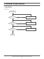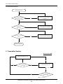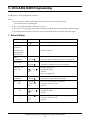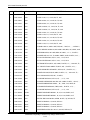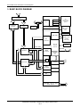
1
Cellular Phone
SCH-A302
SERVICE
Cellular Phone
Manual
CONTENTS
1. Specification
2. Trouble Shooting
3. Tune-up Procedure &
Test Procedure list
4. Frequency Synthesizer Circuit &
Spurious Radiation
Suppression Circuit
5. NAM Programming
6. Electrical Parts List
7. Exploded Views & Parts List
8. Block Diagram
9. PCB Diagrams
10. Circuit Description &
Circuit Diagrams
ELECTRONICS
©Samsung Electronics Co.,Ltd. December. 2001
Pinted in Korea.
Code No.: GH68-02488A
BASIC.
1. SCH-A302 Specification (REF TIA/EIA/IS-137-A-1)
1. GENERAL
ITEM
CDMA
TX Freq. Range
824 ~ 849 MHz
RX Freq. Range
869 ~ 894 MHz
Channel Bandwidth
1.23 MHz
Channel Spacing
30 kHz
Number of Channels
20 FA
Duplex Separation
45 MHz
In/Output Impedance
50 Ω
TX Intermediate Freq.
130.38 MHz
RX Intermediate Freq.
85.38 MHz
TX Local Freq.
1st(FTX + 130.38 MHz)
2nd(260.76 MHz)
1st(FTX + 210.38 MHz)
RX Local Freq.
2nd(170.76 MHz)
TCXO freq.
19.68 MHz
Freq. Stability
(FRX - 45 MHz) ± 350 Hz
Operating Temperature
-30 °C ~ +60 °C
Supply Voltage
+ 3.8 V
SMALL : 81 x 42 x 21 mm 84 g
Size and Weight
MIDDLE : 81 x 42 x 22 mm 87 g
LARGE : 81 x 42 x 25 mm 98 g
SAMSUNG Proprietary-Contents may change without notice
1-1
SCH-A302 Specification
2. 800 MHz CDMA
2-1. GENERAL
TX Freq. Range
824 ~ 849 MHz
RX Freq. Range
869 ~ 894 MHz
Channel Bandwidth
1.23 MHz
Channel Spacing
30 kHz
Number of Channels
20 FA
Duplex Separation
45 MHz
In/Output Impedance
50 Ω
TX Intermediate Frequency
130.38 MHz
RX Intermediate Frequency
85.38 MHz
TX Local Frequency
1st (FTX + 130.38 MHz)
2nd (260.76 MHz)
RX Local Frequency
1st (FRX + 85.38 MHz)
2nd (170.76 MHz)
TCXO Frequency
19.68 MHz
Freq. Stability
(FRX - 45 MHz) ± 150 Hz
Operating Temperature
-30 °C ~ +60 °C
Supply Voltage
+ 3.8 V
2-2. TRANSMITTER
Waveform Quality
0.944 or more
Open Loop Power Control
-25 dBm
-57.5 dBm ~ -38.5 dBm
-65 dBm
-17.5 dBm ~ +1.5 dBm
-104 dBm
+18.0 dBm ~ +30.0 dBm
Minimum TX Power Control
Below -50 dBm
Closed Loop TX Power Control Range
± 24 dB
Maximum RF Output Power
200 mW (+24.5 dBm)
Occupied Band Width
1.32 MHz
Conducted Spurious Emission @900 kHz
-42 dBc / 30 kHz
@1.25 MHz
-54 dBc / 30 kHz
SAMSUNG Proprietary-Contents may change without notice
1-2
SCH-A302 Specification
2-3. RECEIVER
Rx Sensitivity and Dynamic Range
-104 dBm, FER=0.5 % or less
-25 dBm, FER=0.5 % or less
Conducted Spurious Emission
869 ~ 894 MHz
< -81 dBm
824 ~ 849 MHz
< -61 dBm
All other Frequencies
< -47 dBm
Single Tone Desensitization
Rx Power level -101 dBm
Tone Power level -30 dBm
Lower than 1 %
Tone Offset from Carrier ± 900 kHz
Intermoculation Spurious Response Attenuation
Tone 1 offset from carrier = ± 900 kHz
Tone 2 offset from carrier = ± 1,700 kHz
-Test 1, 2
Rx power = -101 dBm
Tone 1 power = -43 dBm
Tone 2 power = -43 dBm
-Test 3, 4
Lower than 1 %
Rx power = -90 dBm
Tone 1 power = -32 dBm
Tone 2 power = -32 dBm
-Test 5, 6
Rx power = -79 dBm
Tone 1 power = -21 dBm
Tone 2 power = -21 dBm
SAMSUNG Proprietary-Contents may change without notice
1-3
2. SCH-A302 Trouble Shooting
1. Logic Section
1-1. No Power
Press PWR button
U501 pin38 Input=HIGH
N
Check Q507, Q509 and its
neighboring circuits
N
Check U501 pin6 & pin10 and its
neighboring circuits
N
Check R536 and its neighboring
circuits
Y
U501 pin6 & pin10
output=2.8 V?
Y
U501 pin39
Input=HIGH?
Y
END
SAMSUNG Proprietary-Contents may change without notice
2-1
SCH-A302 Trouble Shooting
1-2. Abnormal Initial Operation
Press PWR Key
TCXO CLK
applied to U609 pina17/U404
pin7?
N
Check VCTCXO output.
Replace if required.
N
Check OSC401 and its neighboring
circuits. Replace if required.
N
Check OSC401 and its neighvoring
circuits. Replace if required.
N
Check OSC402 and its neighvoring
circuits. Replace if required.
N
Check the LED and its neighboring
circuits. Replace if required.
N
Check the LCD pins and its
neighboring circuits. Replace if
required.
Y
TCXO CLK
signal outputted from OSC401
pin3?
Y
TCXO CL
signal outputted from OSC401
pin4?
Y
TCXO CL
signal outputted from OSC402
pin4?
Y
LED on?
Y
Normal initial
display on LCD?
Y
END
SAMSUNG Proprietary-Contents may change without notice
2-2
SCH-A302 Trouble Shooting
1-3. Abnormal Backlight Operation
Press any button on the phone
‘L’ level outputted
from U501 pin1?
N
Check U501 pin1 and its neighboring
circuits. Replace if required.
N
Check U501 pin1 and its neighboring
circuits. Replace if required.
N
Check keypad dom switch.
Replace if required.
Y
‘L’ level outputted
from U501 pin2?
Y
Backlight LED on
1-4. Abnormal Key Data Input
Check initial status
Scanning signals
outputted from U609 pins C2,
A3, E4, D3, C1?
Y
END
SAMSUNG Proprietary-Contents may change without notice
2-3
SCH-A302 Trouble Shooting
1-5. Abnormal Keytone
Abnormal Keytone
CLK wavefrom outputted
from U609 pin L16 & pin M17?
N
Check the U609 pin and its
neighboring circuits.
Replace if required.
N
Resolder CON500 and its neighboring
circuits. Replace if required.
N
Check C631. Replace if required.
N
Replace the SPK assembly.
Y
CLK waveform outputted
from CON500 pin 5?
Y
Key tone waveform
applied to C561?
Y
Normal Keytone?
Y
END
SAMSUNG Proprietary-Contents may change without notice
2-4
SCH-A302 Trouble Shooting
1-6. Abnormal Alert Tone
Abnormal Keytone
CLK waveform outputted
from U609 pin C14.
N
Check the U609 pin and its
neighboring circuits. Replace if
required.
N
Check R552, Q511 and its neighboring
circuits. Replace if required.
N
Connect the buzzer correctly.
Y
CLK waveform applied to
Q511 Base?
Y
Is the buzzer connection
correct?
Y
Check the buzzer and
replace if required.
2. Transmitter Section
Turn On Max PWR
Abormal transmitter section
N
N
Check U204 TX RFT
out level OK?
Y
Check U402 local level.
-10~0 dBm
Y
N
Check U201 PWR AMP
out level OK?
CDMA : 25~26 dBm
SAMSUNG Proprietary-Contents may change without notice
2-5
SCH-A302 Trouble Shooting
3. Receiver Section : CDMA MODE
Start CDMA mode
Normal CDMA
SVC & ROAM OK?
N
Check CDMA Rx path.
N
Check Transmitter.
Y
Setup CDMA call.
OK?
Y
Measure CDMA FER
N
Normal CDMA RF?
SAMSUNG Proprietary-Contents may change without notice
2-6
SCH-A302 Trouble Shooting
4. Repair Guide
4-1. TX Part Check Point
Using commands in test mode
-01, 09 (0363), 07, 34, 71 (380)
(1) 130.38 MHz (TX IF) output line
- RFT3100 (U204) PIN #14,#15 (about -30 dBm)
- IF TXIF problem Then Check TX 2nd LOCAL (260.76 MHz)
- TX 2nd LOCAL check - RFT 3100 PIN #19 (about 23 dBm)
(2) TXRF (824~849 MHz) out lines.
From RFT3100 (U204) pin #15 to CELLA_OUT
- F201 input and output is ok? - Pin #2 and #5 (about 16 dBm)
- PAM input is ok? U201 pin #2 (about 20 dBm)
- PAM voltage is ok? U201 pin #3 (3 V), 1,4 (3.7 V)
- PA output is ok? U201 pin #5 (about +10 dBm)
- Duplex input and out put is ok? Duplex input is same with PAM output.
Output is You can check CN302 #2 (about 10 dBm)
4-2. RX Part Check Point
(1) RX RF (869~894 MHz) Signal input lines.
- HP Equipment setting
- RF ch 363 (RX:880.89 MHz, TX:835.89 MHz)- at CALL CTRL MENU
- sctr A pwr : -25 dBm (for more easy to check use Spectrum Analyzer)
- Rf Lvl offset : -1.4 at config screen
- Spectrum Analyzer Setting
- center Freq: 880.89 MHz (when check RXRF in 363 Ch)
- span : 5 MHz
- RF input line from Duplex to Mixer check point
- CN302 input and Duplex out (You can check Duplex out at C652) is ok?
- LNA (U360)input ,output and operating voltage is ok?
:Operating voltage-pin#1 (2.5 v) in & out (#3 66 dBm,#4 49 dBm)
- F303 input and output is ok? #2,#5 (about 50 dBm)
- RX Mixer (U361) input is ok? #1 (about 49 dBm)
(2) RF IF circuit (Received RXRF Signal + 1st local = RX IF (85.38 MHz fixed)
- 1st local is ok? U361 #4,#5 (about 13 dBm)
- Voltage is ok? U361 pin #3 3.0v
- Mixer output is ok? U361 pin #6 RXIF (85.38 Mhz-fixed) (about 50 dBm)
- F301 input and output is ok?
(3) IFR (U302) neighbor circuit
- IF input is ok? U300 pin #11,12 (about 75 dBm)
- RX 2nd local is ok? U300 pin #21,22 (about 25 dBm)
- 3.0 V IF (3.0IF) lines are ok? IFR operating voltage
SAMSUNG Proprietary-Contents may change without notice
2-7
SCH-A302 Trouble Shooting
4-3. PLL Part Check Point
(1) VCO (Voltage Controlled Oscillator)
- Operating voltage is ok? OSC402 pin #7
- VT voltage is ok? OSC402 pin #5 (VT voltage was changed according to CH)
- Out is ok? OSC402 pin#1 output 1st local frequency each CH
(2) PLL(Phase Looped Lock)
- Operating voltages are ok? It use + 3.0 VR lines voltages
- TCXO_IN input is ok? U402 pin#8 It use TCXO Freq (19.68 MHz) for Reference.
4-4. Power Line Check Point
(1) U501 VBATT - #4 check
Reset - #B7 check
(2) X501 (Sleep X-tal) 32.768 MHz (pk-pk 2.7 v)
(3) TCXO(OSC401) 19.68 MHz
(4) IFR3000(U302) - #37 check TCXO-N (4.96 MHz) TCXO/N
#38 check CHIP X8-(9.84 MHz)
4-5. Reference Regulators
PM1000 U501
RESET : B7 RESET SIGNAL OUT
3.0_RX : H5 - RX CIRCUIT OPERATING VOLTAGE
3.0_TX : G5 TX CIRCUIT OPERATING VOLTAGE. (Controlled By Idle Signal)
3.0_IF : H7 RFT3100,IFR3000 AND Etc.
4-6. SAMPLING REPAIR RESULT (SCH-A302)
(1) No.1 : 24108148669 Tx Power Problem
- TX IF does not out from RFT3100 (U204) pin#1,2.
- 2nd local and operating voltages (3.0 IF,3.0 VR,VDC) are ok.
- Estimated factor: IFT After replace IFT It working ok.
(2) No.2 : 24108205255 - Tx Power Problem
- TX IF does not out from RFT3100 (U402)pin#6,7.
- 2nd local and operating voltages (3.0_MP, 3.0_TX, 3.0_TX_IF, 3.0_TXRF, 3.0_TX_LO) are ok.
- PA ON signal does not out from MSM.
- MSM also failed to J-TAG Tester.
- Estimated factor: MSM defect
SAMSUNG Proprietary-Contents may change without notice
2-8
SCH-A302 Trouble Shooting
(3) No.3 : 24108167813 - Tx Power Problem
- All TX path is good from RFT 3100 to Mixer input port.
- Mixer output is lower than normal status.
- 1st local and operating voltages are ok.
- TX AGC ADJ voltage is too low.
- Estimated factor: Chip capacitor (C203) which connect to TX AGC ADJ
voltage line C203 Replace ok.
(4) No.4 : Tx Power Problem
- All TX path and voltages are ok from Duplex input to RFT3100 input
- CELLA_OUT (-pin#17) is ok, But U201 RF_IN (-pin#2)is not good.
- Estimated factor : F201 Replace ok.
(5) No.5 : 24108146584 When touch MSM, RX RSSI value has lost.
- All RX path is good from Duplex to Mixer input port .
- 1st local & TCXO did not oscillate.
- TCXO upper case pushed then case and inside components were short when B'D is twisted.
Estimated factor : TCXO After replace TCXO It working ok.
(6) No.6 : 24108221088 - Problem with display (When power on, display was abnormal working)
- LCD and neighbor patterns are ok.
- Estimated Factor: Broken data which is in E2PROM. Data Rebuilding OK
(7) No.7 : 24108134768 - RX problem (No SVC)
- Handset doe not acquire SVC then searching CH repeat very quickly.
- All RX value is good at Rx Part Check Point.
- Ec/Io value (in debug screen) is bad.
- Estimated factor : MSM does not decode receiving signal.
(8) No.8 : No Power on (Can't not power on)
- X501 Sleep X-tal (32.768 MHz) is O.K
- V_DC 3.0V is O.K
- CHIP X8 No output IFR #38
- TCXO_N No output IFR #37
- TCXO Not oscillator Pin # 3
- TCXO crack : TCXO replace O.K
(9) No.9 : 24108233382 - ESN INVALID
- ESN No was broken : 0000000
- ESN data at E2PROM was broken caused ESD or Electric shock.
- E2PROM replace and rewriting ESN number.
SAMSUNG Proprietary-Contents may change without notice
2-9
3. SCH-A302 Tune-up Rrocedure & Test Procedure list
1. List of Equipment
• DC Power Supply
• Test Jig : HHP I/F TESTJIG GH80-10502C
• Test Cable : GH3900052A
• RF Cable : GH3900075A
• CDMA Mobile Station Test Set HP8924C, HP83236A, CMD-80, etc
• Spectrum Analyzer(include CDMA Test Mode) HP8596E
2. Configuration of Test
Spectrum Analyzer
RF IN
RF cable
HP8924C
RF
IN/OUT
Audio Audio
OUT
IN
DUT
Directional
Coupler
Data cable
Test Jig
To A-Out
To A-In
DC Power Supply
(+3.93 V)
• CAUTION : The test jig and data cable has a voltage drop of 0.15 V at FM Max power output,
you’d better set the DC power supply is 3.8 V for normal test condition.
(Nominal voltage of battery is 3.8 V at cellular phone)
SAMSUNG Proprietary-Contents may change without notice
3-1
SCH-A302 Tune-up Rrocedure & Test Procedure list
3. Test Cable Description for SCH-A302
3-1. Test Cable
1
5
3
4
2
6
3-2. Test Cable Connections
1
MHC 172
2
RF CABLE (1.4 dB Loss for CDMA800 and AMPS, 2.1 dB Loss for PCS)
3
BNC CONECTOR (RF)
4
PLUG CONNECT TO SCH-A302
5
DATA CABLE
6
Dsub 25PIN CONNECTOR (DATA)
Change to Test Mode
A. To Change the phone’s state from Normal Mode to Test Mode, You should enter the following keys.
: Press [ 7 5 9 # 8 1 3 5 8 0 "(A+Y)"]
B. The Command “2 1” is mode and channel change.
“20363”
Channel number
Mode : CDMA
and Push the [OK] Key to save.
C. The command “0 1” is Suspend.
D. To finish the Test Mode, You should enter the command “0 2”.
Channel Selection and Tx Power Output Level Control
1. CDMA
A. Enter to Test Mode [
7 5 9 # 8 1 3 5 8 0 "(A+Y)"]
B. The command “2 1” is mode and channel change.
“20363”
Channel number
Mode : CDMA
Push the [OK] Key to save.
SAMSUNG Proprietary-Contents may change without notice
3-2
SCH-A302 Tune-up Rrocedure & Test Procedure list
C. “0 1” : Suspend.
D. “2 1 + 2 0 3 6 3 ‘#’ “ : Set to ‘0363’ channel.
E. “0 7” “ Carrier On.
F. “3 4” : Spread spectrum to 1.23 MHz band width.
G. “7 1
“ : Adjust RF power level.
Set the acurate power with press ‘SEND’ (power growing up) or ‘END’ (power growing down).
“
“ means AGC level and AGC level range is from 000 to 511.
2. CDMA
TEST ITEMS
PROCEDURE
1. PREPARANCE
Set test equipments up.
[ 7 5 9 # 8 1 3 5 8 0 "(A+Y)"] : Enter the Test Mode
“0 1” : Suspend
Confirm that the phone is in te “CDMA Mode”.
(If not CDMA Mode, Use Test COMMAND “21” “2XXXX” and Push
the [OK] Key to “save”, and enter “0 2” to restart)
If you select a wrong key, press “CLR”, then enter new command.
To exit the Test Mode at any time, just press [0 2].
2. FREQUENCY
ACCURACY
“0 1” : Suspend.
“0 9 + 0 3 6 3 ‘#’ ” : Set channel to 363.
“0 7” : Carrier On.
“3 4” : Spread spectrum.
“7 1 3 0 0 ‘#’ ” : Set AGC level.
Measure the TX frequency : 836.49 MHz ± 300 Hz.
3. OCCUPIED CDMA
BANDWIDTH
“0 1” : Suspend.
“0 9 + 0 3 6 3 ‘#’ ” : Set channel to 383.
“0 7” : Carrier On.
“3 4” : Spread spectrum.
“7 1 X X X ‘#’ ” : Enter AGC Code(XXX) to adjust RF Output Power.
Measure the bandwidth (spec : 1.23 MHz)
4. LIMITATIONS ON
EMISSIONS
“0
“0
“0
“3
“7
1” : Suspend.
9 + 0 3 6 3 ‘#’ ” : Set channel to 363.
7” : Carrier On.
4” : Spread spectrum.
1 X X X ‘#’ ” : Enter AGC Code(XXX) to adjust RF Output Power.
Measure the spurious at Fc ± 900 kHz, Fc ± 1.98 MHz, 2Fc, 3Fc, 1/2Fc.
spec : Fc ± 900 kHz below 42 dBc / 30 kHz
Fc ± 1.98 kHz below 54 dBc / 30 kHz
Outside Receive Band 43 + 10 log (PY)
PY : Mean Output Power in watts
SAMSUNG Proprietary-Contents may change without notice
3-3
SCH-A302 Tune-up Rrocedure & Test Procedure list
3. CDMA Test Procedure
(1) PREPARATION
(2) FREQUENCY ACCURACY
Set to HP8924c auto test mode.
Then run auto test.
See the auto test result.
(3) OCCUPIED CDMA BANDWIDTH
Before call condition.
1 HP8924c call control screen.
1. RF channel : equal to CDMA terminal.
2. Protocol : IS-95a
3. RF CH STD : MS AMPS
4. Traffic data mode : SVC OPT 2
5. Data rate : full rate
6. Power : avg power
7. Sector a power : -75 dBm
2 Range screen setting
8. Piolot : -7 dBm
9. Traffic : -7.4 dBm
10.Pwr cotl : always up
3 Config screen(shift + test)
1. RF level offset : on
2. RF in/out : -1.4 dBm
4 Etc
1. Test cable loss : -1.4 dBm
2. Splitter loss : input measured loss
A method of measurement
1 Call control screen
1. HP8924C channel equal to CDMA terminal.
2. Send call
Power : Always up.
Sector A power : -104 dBm
3. Spectrum analyser
Mode : cdma analyser - Freq - occupy bandwidth - occupied
4. Read Max power
(4) LIMITATIONS ON EMISSIONS
Before call control
1 HP8924C call control screen
1. RF channel : Equal to CDMA terminal
2. Protocol : IS-95a
3. RF CH STD : MS AMPS
4. Traffic data mode : SVC OPT 2
5. Data Rate : FULL Rate
6. Power : CH power
7. Sector A power : -60 dBm
8. PWR COTL : CLOSED LOOP
SAMSUNG Proprietary-Contents may change without notice
3-4
SCH-A302 Tune-up Rrocedure & Test Procedure list
2
3
1
2
Config Screen (shift + test) screen
1. RF Level Offset : ON
2. RF In/Out : Input measured LOSS
ETC
1. Test cable loss : -1.4 dBm
2. SPLITTER : Input measured loss
A method of measurement
Call control screen
1. HP8924C channel equal to CDMA terminal.
2. Send call
3. Spectrum analyser
Mode : cdma analyser - more - more - xmtr spurious-spurious close
Measure -13 dB spurious
4. Change segment F-, F+, Fc then check wave form quality
Specification
"A" is pass, or when "A" was fail, "B" and "C" must pass.
IN BAND
Center
Frequency
OFF set
OUT BAND
*30 kHz bandwidth-over 900 kHz
*1 MHz bandwidth-over 1.385 MHz
*30 kHz bandwidth-over 1.98 MHz
*1 MHz bandwidth-over 2.465 MHz
(A) -42dBc / 30kHz
(A) -54dBc / 30kHz
(B) -60dBc / 30 kHz
(B) -60dBc / 30 kHz
(C) -55dBm / 30 kHz
(C) -55dBm / 30 kHz
4. Download New software
To download program, you need to connect your pc and mobile using data link cable or jig
box. Please make sure your phone is in DM mode ( menu 4 -> 9 ) before you are using
Ndloader. (It is easier this way)
(1) Connect your pc and handset using data link cable or jig box.
(2) Power on the phone. Please check that the phone is in DM mode. (Menu->4->9).
If it is in Handsfree mode, please change it to DM mode and press ok.
The phone will be restarted.
(3) Run the Ndloader.
(4) To make sure that your phone is connected with Ndloader, click ? icon on the program,
you would get the phone information.
(5) Click folder icon on the Ndloader to choose new binary file to download.
You will see the file information.
(6) On the right middle of Ndloader, you will see download types. Choose Normal.
(7) Now you are ready to download new software.
Then Click download icon ( the green runner ) to start download. Please wait until download is done.
If download is completed properly, the phone will be restarted.
SAMSUNG Proprietary-Contents may change without notice
3-5
4. SCH-A302 Frequency Synthesizer Circuit &
Spurious radiation suppression circuit
1. Frequency Synthesizer Circuit
The Frequency synthesizer is an indirect frequency synthesizer PLL(Phased Locked Loop).
It consists of a VCTCXO(OSC401), PLL, VCO (OSC402, U402), and loop filter.
VCTCXO
The VCTCXO is a reference source of the frequency synthesizer. It provides 19.68MHz reference frequency
to PLL, VCO (OSC402, U402). The VCTCXO is a Voltage Controlled Temperature Compensated Crystal
Oscillator having 19.68 MHz ± 2.5 ppm frequency stability over all useful temperature range. A correct
frequency tuning is made by the control voltage.
VCO, PLL
The PLL, VCO Module(OSC402, U402) generates the signal having 966 ± 12.5 MHz center frequency with
the voltage control. The PLL, VCO (OSC402, U402) controls this signal.
The PLL, VCO Module(OSC402, U402) includes prescalers and charge pump. The reference divider in the
PLL, VCO Module(OSC402, U402) divides the frequency of VCTCXO by 1968 and makes reference
frequency 10kHz. This reference frequency is supplied to one of the input of phase detector. The signal
generated at the PLL, VCO Module(OSC402, U402) goes into another input stage of the phase detector
through a prescaler and the main divider.
At this point, the error proportional to the phase difference of two inputs is occurred.
This error signal is supplied to the frequency control input stage of the PLL, VCO (OSC402, U402) through
the loop filter consisted RC.
SAMSUNG Proprietary-Contents may change without notice
4-1
SCH-A302 Frequency Synthesizer circuit & Spurious radiation suppression circuit
2. Spurious Radiation Suppression Circuit
The spurious signal from antenna is suppressed at the duplexer. The duplexer has a flat characteristics to
the receive signal and a high attenuation characteristics to the harmonic signal of transmission.
So it suppress the spurious radiation
Table: The characteristic of CDMA duplexer filter(F302)
PARAMETER
VALUE
TX
Center Frequency
836.5 MHz (FT)
Bandwidth
FT ± 12.5 MHz
Insertion Loss at BW
3.0 dB Max
VSWR at BW
1.8 Max
Input power
3.0 W Max
Attenuation
869 ~ 894 MHz
Ripple at BW
1.6 dB Max
40 dB Min
RX
Center Frequency
881.5 MHz (FR )
Bandwidth
FR ± 12.5 MHz
Insertion Loss at BW
4.0 dB Max
VSWR at BW
1.8 Max
Input power
1 W Max
Attenuation
824 ~ 849 MHz
Ripple at BW
2.0 dB Max
56 dB Min
T X to R X
Isolation
824 ~ 849 MHz
55 dB Max
869 ~ 894 MHz
49 dB Max
SAMSUNG Proprietary-Contents may change without notice
4-2
5. SCH-A302 NAM Programming
NAM features can be programmed as follows:
Notes:
• If you enter the NAM program mode, each item shows the currenly stored data.
Go to the next item by pressing OK.
• You can modify the data by entering a new data.
• If you enter a wrong digit, press CLR to delete the last digit. Press and hold CLR to delete all digits.
• To scroll items backwards or forwards, press the VOLUME button on the left side of the phone.
1. General Setup
LCD Display
Key in
Function
47 869#08#9
-selects NAM programming
1
-Choose ‘General’
ESN
B0000000
Volume
-Electronic Serial Number of the phone is displayed
CAI version
3
Volume
-Common Air Interface version is displayed
NAM Program
1:General
2.NAM1 Setup
3:NAM2 Setup
4:Advanced
13K EVRC/8K
13K voice
or #
OK
SCM
01101010
Lock Code
0000
Volume
-Station Class Mark displays the power class,
transmission, slotted class, dual mode.
Volume
4-digit code
OK
Lock code, current status is displayed
-to change, enter new code.
-stores it
Slot Mode
Yes
Slot Index
2
Vocoder sample rate
-changes the status.
-stores it.
-8K is not supported.
OK
Slot mode. ‘Yes’ indicates the slot mode.
-changes the status.
-stores it.
Volume
0~7
OK
Slot mode index. The higher,the longer sleeping time
-to change, enter new one.
-stores it.
or #
SAMSUNG Proprietary-Contents may change without notice
5-1
SCH-A302 NAM Programming
2. Setting Up NAM
LCD Display
Key in
Function
NAM Program
1:General
2.NAM1 Setup
3:NAM2 setup
4:Advanced
2
-Choose ‘NAM1 Setup’
CDMA TEL NO.
3003003000
number
OK
MIN1,MIN2 is displayed
-to change, enter new one.
-stores it.
IMSI MCC
000
number
OK
IMSI Moble Country Code,current code is displayed.
-to change, enter new one.
-stores it.
IMSI MNC
00
number
OK
IMSI Moble Network Code,current code is displayed.
-to change, enter new one.
-stores it.
SYSTEM
Standard
OK
- Only ‘Standard’ mode is supported.
class number
OK
CDMA Access Overload Class,current status is
displayed.
-to change,enter new one.
-stores it.
ACCOLC
0
Pchn Sys A
000
Pchn Sys B
000
Schn Sys A
000
Schn Sys B
000
LockoutSID 1~10
0000
CDMA HOME SID
Yes
channel number
OK
Primary CDMA Channel for System A is displayed
-to change, enter new one.
-stores it.
channel number
OK
Primary CDMA Channel for System B is displayed
-to change, enter new one.
-stores it.
channel number
OK
Secondary CDMA Channel for System A is displayed
-to change, enter new one.
-stores it.
channel number
OK
Secondary CDMA Channel for System B is displayed
-to change, enter new one.
-stores it.
SID number
OK
CDMA SID to lockout is displayed
-to change, enter new one.
-stores it.
# or
OK
CDMA Home system ID, current value is displayed.
-changes the status.
-stores it.
SAMSUNG Proprietary-Contents may change without notice
5-2
SCH-A302 NAM Programming
LCD Display
Key in
CDMA fSID
Yes
CDMA fNID
Yes
HomeSID #1 ~ #4
4120
HomeNID #1 ~ #4
65535
Function
# or
OK
CDMA foreign SID, current value is displayed.
-changes the status.
-stores it.
# or
OK
CDMA foreign NID, current value is displayed.
-changes the status.
-stores it.
number
OK
CDMA HOME SIDs written in the list, current value is
displayed.
-to change, enter new one.
-stores it.
number
OK
CDMA HOME NIDs written in the list, current value is
displayed.
-to change, enter new one.
-stores it.
SAMSUNG Proprietary-Contents may change without notice
5-3
6. SCH-A302 Electrical parts list
Level
SEC CODE
Design LOC
DESCRIPTIONS
0
GH92-00996A
1
GH41-00192A
PCB-SCHA302 MAIN SCH-A302, -, 6L, -, 0.7T, 100 x 138 mm, -, 3, -, -
1
GH71-00052A
NPR-ANT.CONTACT SCH-A100, BE-CU, T0.1, AU
1
GH73-00214A
RMO-ANTENNA RUBBER SPH-A1000, RUBBER, 2 x 3 x T0.5, BLK, 50
1
GH73-00442A
RMO-BUZZER HOLDER SCH-A300, RUBBER, -, BLK, 50, -
1
GH74-00843A
MPR-FPCB CUSHION SCH-A8800, 71TS, T3, BRN, -
1
GH74-00892A
MPR-SHIELD TAPE 5 SCH-A8800, TAPE, T0.14, -, -
1
GH74-00898A
MPR-SHIELD TAPE 6 SCH-A300, -, 6 x 4, S/BLU, -
1
3002-001101
AU501
BUZZER-MAGNETIC 88 dB, 3.6 V, 100 mA, 2550 Hz, TP
1
2203-000254
C101
C-CERAMIC, CHIP 10 nF, 10 %, 16 V, X7R, TP, 1005, -
1
2203-000995
C102
C-CERAMIC, CHIP 0.047 nF, 5 %, 50 V, NP0, TP, 1005
1
2203-000254
C103
C-CERAMIC, CHIP 10 nF, 10 %, 16 V, X7R, TP, 1005, -
1
2203-000940
C104
C-CERAMIC, CHIP 470 pF, 10 %, 50 V, X7R, TP, 1005, -
1
2203-000940
C105
C-CERAMIC, CHIP 470 pF, 10 %, 50 V, X7R, TP, 1005, -
1
2203-000254
C106
C-CERAMIC, CHIP 10 nF, 10 %, 16 V, X7R, TP, 1005, -
1
2203-005061
C107
C-CERAMIC, CHIP 100 nF, +80-20 %, 16 V, Y5 V, TP, 1005
1
2203-005061
C108
C-CERAMIC, CHIP 100 nF, +80-20 %, 16 V, Y5 V, TP, 1005
1
2203-000254
C109
C-CERAMIC, CHIP 10 nF, 10 %, 16 V, X7R, TP, 1005, -
1
2203-000233
C110
C-CERAMIC, CHIP 0.1 nF, 5 %, 50 V, NP0, TP, 1005
1
2203-005061
C111
C-CERAMIC, CHIP 100 nF, +80-20 %, 16 V, Y5 V, TP, 1005
1
2203-000233
C112
C-CERAMIC, CHIP 0.1 nF, 5 %, 50 V, NP0, TP, 1005
1
2203-005061
C113
C-CERAMIC, CHIP 100 nF, +80-20 %, 16 V, Y5 V, TP, 1005
1
2203-000940
C114
C-CERAMIC, CHIP 470 pF, 10 %, 50 V, X7R, TP, 1005, -
1
2203-000940
C115
C-CERAMIC, CHIP 470 pF, 10 %, 50 V, X7R, TP, 1005, -
1
2203-000254
C116
C-CERAMIC, CHIP 10 nF, 10 %, 16 V, X7R, TP, 1005, -
1
2203-000233
C117
C-CERAMIC, CHIP 0.1 nF, 5 %, 50 V, NP0, TP, 1005
1
2203-000233
C118
C-CERAMIC, CHIP 0.1 nF, 5 %, 50 V, NP0, TP, 1005
1
2203-000438
C119
C-CERAMIC, CHIP 1 nF, 10 %, 50 V, X7R, TP, 1005, -
1
2203-000438
C120
C-CERAMIC, CHIP 1 nF, 10 %, 50 V, X7R, TP, 1005, -
1
2203-000438
C121
C-CERAMIC, CHIP 1 nF, 10 %, 50 V, X7R, TP, 1005, -
1
2203-005061
C122
C-CERAMIC, CHIP 100 nF, +80-20 %, 16 V, Y5 V, TP, 1005
1
2203-000254
C123
C-CERAMIC, CHIP 10 nF, 10 %, 16 V, X7R, TP, 1005, -
1
2203-005061
C124
C-CERAMIC, CHIP 100 nF, +80-20 %, 16 V, Y5 V, TP, 1005
SAMSUNG Proprietary-Contents may change without notice
6-1
SCH-A302 Electrical parts list
Level
SEC CODE
Design LOC
DESCRIPTIONS
1
2203-000438
C125
C-CERAMIC, CHIP 1 nF, 10 %, 50 V, X7R, TP, 1005, -
1
2203-000438
C126
C-CERAMIC, CHIP 1 nF, 10 %, 50 V, X7R, TP, 1005, -
1
2203-000438
C127
C-CERAMIC, CHIP 1 nF, 10 %, 50 V, X7R, TP, 1005, -
1
2203-000254
C128
C-CERAMIC, CHIP 10 nF, 10 %, 16 V, X7R, TP, 1005, -
1
2203-000714
C129
C-CERAMIC, CHIP 3.3 nF, 10 %, 50 V, X7R, TP, 1005, -
1
2203-000254
C140
C-CERAMIC, CHIP 10 nF, 10 %, 16 V, X7R, TP, 1005, -
1
2203-005061
C142
C-CERAMIC, CHIP 100 nF, +80-20 %, 16 V, Y5 V, TP, 1005
1
2203-005061
C143
C-CERAMIC, CHIP 100 nF, +80-20 %, 16 V, Y5 V, TP, 1005
1
2203-000254
C144
C-CERAMIC, CHIP 10 nF, 10 %, 16 V, X7R, TP, 1005, -
1
2203-000940
C145
C-CERAMIC, CHIP 470 pF, 10 %, 50 V, X7R, TP, 1005, -
1
2203-000254
C146
C-CERAMIC, CHIP 10 nF, 10 %, 16 V, X7R, TP, 1005, -
1
2203-000438
C147
C-CERAMIC, CHIP 1 nF, 10 %, 50 V, X7R, TP, 1005, -
1
2203-000438
C150
C-CERAMIC, CHIP 1 nF, 10 %, 50 V, X7R, TP, 1005, -
1
2203-000438
C151
C-CERAMIC, CHIP 1 nF, 10 %, 50 V, X7R, TP, 1005, -
1
2203-000438
C152
C-CERAMIC, CHIP 1 nF, 10 %, 50 V, X7R, TP, 1005, -
1
2404-001017
C160
C-TA, CHIP 1 uF, 20 %, 10 V, GP, TP, 2012, 2, 0
1
2203-000940
C161
C-CERAMIC, CHIP 470 pF, 10 %, 50 V, X7R, TP, 1005, -
1
2203-000940
C162
C-CERAMIC, CHIP 470 pF, 10 %, 50 V, X7R, TP, 1005, -
1
2203-000628
C201
C-CERAMIC, CHIP 0.022 nF, 5 %, 50 V, NP0, TP, 1005
1
2203-005061
C202
C-CERAMIC, CHIP 100 nF, +80-20 %, 16 V, Y5 V, TP, 1005
1
2203-000885
C203
C-CERAMIC, CHIP 4.7 nF, 10 %, 25 V, X7R, TP, 1005, -
1
2203-000995
C204
C-CERAMIC, CHIP 0.047 nF, 5 %, 50 V, NP0, TP, 1005
1
2203-000254
C205
C-CERAMIC, CHIP 10 nF, 10 %, 16 V, X7R, TP, 1005, -
1
2203-000233
C207
C-CERAMIC, CHIP 0.1 nF, 5 %, 50 V, NP0, TP, 1005
1
2203-000254
C208
C-CERAMIC, CHIP 10 nF, 10 %, 16 V, X7R, TP, 1005, -
1
2203-001598
C209
C-CERAMIC, CHIP 2200 nF, +80-20 %, 16 V, Y5 V, TP, 2012
1
2203-005503
C210
C-CERAMIC, CHIP 0.18 nF, 5 %, 25 V, NP0, TP, 1005
1
2203-005503
C211
C-CERAMIC, CHIP 0.18 nF, 5 %, 25 V, NP0, TP, 1005
1
2203-001598
C213
C-CERAMIC, CHIP 2200 nF, +80-20 %, 16 V, Y5 V, TP, 2012
1
2203-000254
C214
C-CERAMIC, CHIP 10 nF, 10 %, 16 V, X7R, TP, 1005, -
1
2203-000233
C215
C-CERAMIC, CHIP 0.1 nF, 5 %, 50 V, NP0, TP, 1005
1
2203-000995
C216
C-CERAMIC, CHIP 0.047 nF, 5 %, 50 V, NP0, TP, 1005
1
2203-000254
C217
C-CERAMIC, CHIP 10 nF, 10 %, 16 V, X7R, TP, 1005, -
1
2203-001072
C218
C-CERAMIC, CHIP 0.056 nF, 5 %, 50 V, NP0, TP, 1005
SAMSUNG Proprietary-Contents may change without notice
6-2
SCH-A302 Electrical parts list
Level
SEC CODE
Design LOC
DESCRIPTIONS
1
2203-000254
C219
C-CERAMIC, CHIP 10 nF, 10 %, 16 V, X7R, TP, 1005, -
1
2404-001151
C220
C-TA, CHIP 33 uF, 20 %, 6.3 V, LZ, TP, 3216
1
2203-001017
C221
C-CERAMIC, CHIP 0.004 nF, 0.25 pF, 50 V, NP0, TP, 1005
1
2203-001259
C222
C-CERAMIC, CHIP 0.008 nF, 0.5 pF, 50 V, NP0, TP, 1005
1
2203-001072
C223
C-CERAMIC, CHIP 0.056 nF, 5 %, 50 V, NP0, TP, 1005
1
2203-000940
C226
C-CERAMIC, CHIP 470 pF, 10 %, 50 V, X7R, TP, 1005, -
1
2404-001017
C227
C-TA, CHIP 1 uF, 20 %, 10 V, GP, TP, 2012, 2, 0
1
2203-000233
C229
C-CERAMIC, CHIP 0.1 nF, 5 %, 50 V, NP0, TP, 1005
1
2203-000438
C23
C-CERAMIC, CHIP 1 nF, 10 %, 50 V, X7R, TP, 1005, -
1
2203-000254
C230
C-CERAMIC, CHIP 10 nF, 10 %, 16 V, X7R, TP, 1005, -
1
2203-000233
C231
C-CERAMIC, CHIP 0.1 nF, 5 %, 50 V, NP0, TP, 1005
1
2203-001072
C234
C-CERAMIC, CHIP 0.056 nF, 5 %, 50 V, NP0, TP, 1005
1
2203-000438
C235
C-CERAMIC, CHIP 1 nF, 10 %, 50 V, X7R, TP, 1005, -
1
2203-000995
C237
C-CERAMIC, CHIP 0.047 nF, 5 %, 50 V, NP0, TP, 1005
1
2203-000995
C238
C-CERAMIC, CHIP 0.047 nF, 5 %, 50 V, NP0, TP, 1005
1
2203-000386
C240
C-CERAMIC, CHIP 0.015 nF, 5 %, 50 V, NP0, TP, 1005
1
2203-000438
C250
C-CERAMIC, CHIP 1 nF, 10 %, 50 V, X7R, TP, 1005, -
1
2203-001437
C318
C-CERAMIC, CHIP 5 pF, 0.25 pF, 50 V, X7R, TP, 1005, 1.0
1
2203-000254
C320
C-CERAMIC, CHIP 10 nF, 10 %, 16 V, X7R, TP, 1005, -
1
2203-005382
C321
C-CERAMIC, CHIP 0.006 nF, 0.1 pF, 50 V, NP0, TP, 1005
1
2203-001437
C323
C-CERAMIC, CHIP 5 pF, 0.25 pF, 50 V, X7R, TP, 1005, 1.0
1
2203-000438
C331
C-CERAMIC, CHIP 1 nF, 10 %, 50 V, X7R, TP, 1005, -
1
2203-000438
C332
C-CERAMIC, CHIP 1 nF, 10 %, 50 V, X7R, TP, 1005, -
1
2404-001105
C333
C-TA, CHIP 10 uF, 20 %, 6.3 V, GP, TP, 2012
1
2203-000254
C334
C-CERAMIC, CHIP 10 nF, 10 %, 16 V, X7R, TP, 1005, -
1
2203-000233
C335
C-CERAMIC, CHIP 0.1 nF, 5 %, 50 V, NP0, TP, 1005
1
2203-000233
C337
C-CERAMIC, CHIP 0.1 nF, 5 %, 50 V, NP0, TP, 1005
1
2203-000254
C338
C-CERAMIC, CHIP 10 nF, 10 %, 16 V, X7R, TP, 1005, -
1
2203-000885
C339
C-CERAMIC, CHIP 4.7 nF, 10 %, 25 V, X7R, TP, 1005, -
1
2203-000254
C340
C-CERAMIC, CHIP 10 nF, 10 %, 16 V, X7R, TP, 1005, -
1
2203-005061
C341
C-CERAMIC, CHIP 100 nF, +80-20 %, 16 V, Y5 V, TP, 1005
1
2203-000438
C342
C-CERAMIC, CHIP 1 nF, 10 %, 50 V, X7R, TP, 1005, -
1
2203-000359
C343
C-CERAMIC, CHIP 0.15 nF, 5 %, 50 V, NP0, TP, 1005
1
2203-005395
C344
C-CERAMIC, CHIP 0.0047 nF, 0.1 pF, 50 V, NP0, TP, 1005
SAMSUNG Proprietary-Contents may change without notice
6-3
SCH-A302 Electrical parts list
Level
SEC CODE
Design LOC
DESCRIPTIONS
1
2203-000885
C345
C-CERAMIC, CHIP 4.7 nF, 10 %, 25 V, X7R, TP, 1005, -
1
2203-000359
C346
C-CERAMIC, CHIP 0.15 nF, 5 %, 50 V, NP0, TP, 1005
1
2203-005480
C349
C-CERAMIC, CHIP 33 nF, 10 %, 10 V, X7R, TP, 1005, -
1
2404-001086
C350
C-TA, CHIP 4.7 uF, 20 %, 6.3 V, GP, TP, 2012, -
1
2203-005383
C370
C-CERAMIC, CHIP 7 pF, 0.1 pF, 50 V, NPO, TP, 1005, -
1
2203-000628
C371
C-CERAMIC, CHIP 0.022 nF, 5 %, 50 V, NP0, TP, 1005
1
2203-000438
C372
C-CERAMIC, CHIP 1 nF, 10 %, 50 V, X7R, TP, 1005, -
1
2203-000233
C373
C-CERAMIC, CHIP 0.1 nF, 5 %, 50 V, NP0, TP, 1005
1
2203-000696
C375
C-CERAMIC, CHIP 0.002 nF, 0.25 pF, 50 V, NP0, TP, 1005
1
2203-005444
C376
C-CERAMIC, CHIP 0.003 nF, 0.1 pF, 50 V, NP0, TP, 1005
1
2203-000438
C377
C-CERAMIC, CHIP 1 nF, 10 %, 50 V, X7R, TP, 1005, -
1
2203-005061
C378
C-CERAMIC, CHIP 100 nF, +80-20 %, 16 V, Y5 V, TP, 1005
1
2404-001105
C379
C-TA, CHIP 10 uF, 20 %, 6.3 V, GP, TP, 2012
1
2203-000233
C380
C-CERAMIC, CHIP 0.1 nF, 5 %, 50 V, NP0, TP, 1005
1
2203-000278
C381
C-CERAMIC, CHIP 0.01 nF, 0.5 pF, 50 V, NP0, TP, 1005
1
2203-000438
C382
C-CERAMIC, CHIP 1 nF, 10 %, 50 V, X7R, TP, 1005, -
1
2203-005444
C383
C-CERAMIC, CHIP 0.003 nF, 0.1 pF, 50 V, NP0, TP, 1005
1
2203-002443
C384
C-CERAMIC, CHIP 0.33 nF, 10 %, 50 V, X7R, TP, 1005
1
2203-005480
C385
C-CERAMIC, CHIP 33 nF, 10 %, 10 V, X7R, TP, 1005, -
1
2203-005061
C386
C-CERAMIC, CHIP 100 nF, +80-20 %, 16 V, Y5 V, TP, 1005
1
2203-000233
C387
C-CERAMIC, CHIP 0.1 nF, 5 %, 50 V, NP0, TP, 1005
1
2203-005061
C388
C-CERAMIC, CHIP 100 nF, +80-20 %, 16 V, Y5 V, TP, 1005
1
2404-001105
C389
C-TA, CHIP 10 uF, 20 %, 6.3 V, GP, TP, 2012
1
2203-000386
C390
C-CERAMIC, CHIP 0.015 nF, 5 %, 50 V, NP0, TP, 1005
1
2203-000386
C391
C-CERAMIC, CHIP 0.015 nF, 5 %, 50 V, NP0, TP, 1005
1
2203-000233
C392
C-CERAMIC, CHIP 0.1 nF, 5 %, 50 V, NP0, TP, 1005
1
2203-000885
C393
C-CERAMIC, CHIP 4.7 nF, 10 %, 25 V, X7R, TP, 1005, -
1
2203-005061
C394
C-CERAMIC, CHIP 100 nF, +80-20 %, 16 V, Y5 V, TP, 1005
1
2203-000885
C395
C-CERAMIC, CHIP 4.7 nF, 10 %, 25 V, X7R, TP, 1005, -
1
2203-001432
C396
C-CERAMIC, CHIP 47 nF, +80-20 %, 16 V, Y5 V, TP, 1005
1
2404-001105
C397
C-TA, CHIP 10 uF, 20 %, 6.3 V, GP, TP, 2012
1
2203-000438
C398
C-CERAMIC, CHIP 1 nF, 10 %, 50 V, X7R, TP, 1005, -
1
2203-000438
C407
C-CERAMIC, CHIP 1 nF, 10 %, 50 V, X7R, TP, 1005, -
1
2203-000233
C408
C-CERAMIC, CHIP 0.1 nF, 5 %, 50 V, NP0, TP, 1005
SAMSUNG Proprietary-Contents may change without notice
6-4
SCH-A302 Electrical parts list
Level
SEC CODE
Design LOC
DESCRIPTIONS
1
2203-000438
C409
C-CERAMIC, CHIP 1 nF, 10 %, 50 V, X7R, TP, 1005, -
1
2203-000254
C410
C-CERAMIC, CHIP 10 nF, 10 %, 16 V, X7R, TP, 1005, -
1
2203-000233
C411
C-CERAMIC, CHIP 0.1 nF, 5 %, 50 V, NP0, TP, 1005
1
2203-000233
C412
C-CERAMIC, CHIP 0.1 nF, 5 %, 50 V, NP0, TP, 1005
1
2203-000233
C413
C-CERAMIC, CHIP 0.1 nF, 5 %, 50 V, NP0, TP, 1005
1
2203-001072
C414
C-CERAMIC, CHIP 0.056 nF, 5 %, 50 V, NP0, TP, 1005
1
2404-001151
C415
C-TA, CHIP 33 uF, 20 %, 6.3 V, LZ, TP, 3216
1
2203-000725
C416
C-CERAMIC, CHIP 3.9 nF, 10 %, 50 V, X7R, TP, 1005, -
1
2203-005061
C417
C-CERAMIC, CHIP 100 nF, +80-20 %, 16 V, Y5 V, TP, 1005
1
2203-000254
C418
C-CERAMIC, CHIP 10 nF, 10 %, 16 V, X7R, TP, 1005, -
1
2203-000254
C419
C-CERAMIC, CHIP 10 nF, 10 %, 16 V, X7R, TP, 1005, -
1
2203-000585
C420
C-CERAMIC, CHIP 220 pF, 10 %, 50 V, X7R, TP, 1005, -
1
2404-001092
C421
C-TA, CHIP 220 nF, 20 %, 20 V, GP, TP, 2012, -
1
2203-000254
C422
C-CERAMIC, CHIP 10 nF, 10 %, 16 V, X7R, TP, 1005, -
1
2203-000233
C423
C-CERAMIC, CHIP 0.1 nF, 5 %, 50 V, NP0, TP, 1005
1
2203-000233
C424
C-CERAMIC, CHIP 0.1 nF, 5 %, 50 V, NP0, TP, 1005
1
2203-000254
C425
C-CERAMIC, CHIP 10 nF, 10 %, 16 V, X7R, TP, 1005, -
1
2203-000233
C426
C-CERAMIC, CHIP 0.1 nF, 5 %, 50 V, NP0, TP, 1005
1
2203-000278
C427
C-CERAMIC, CHIP 0.01 nF, 0.5 pF, 50 V, NP0, TP, 1005
1
2203-000254
C428
C-CERAMIC, CHIP 10 nF, 10 %, 16 V, X7R, TP, 1005, -
1
2203-000995
C429
C-CERAMIC, CHIP 0.047 nF, 5 %, 50 V, NP0, TP, 1005
1
2203-000233
C431
C-CERAMIC, CHIP 0.1 nF, 5 %, 50 V, NP0, TP, 1005
1
2203-000233
C432
C-CERAMIC, CHIP 0.1 nF, 5 %, 50 V, NP0, TP, 1005
1
2203-000233
C433
C-CERAMIC, CHIP 0.1 nF, 5 %, 50 V, NP0, TP, 1005
1
2203-000254
C435
C-CERAMIC, CHIP 10 nF, 10 %, 16 V, X7R, TP, 1005, -
1
2203-000233
C436
C-CERAMIC, CHIP 0.1 nF, 5 %, 50 V, NP0, TP, 1005
1
2203-000233
C437
C-CERAMIC, CHIP 0.1 nF, 5 %, 50 V, NP0, TP, 1005
1
2203-000233
C438
C-CERAMIC, CHIP 0.1 nF, 5 %, 50 V, NP0, TP, 1005
1
2203-000254
C501
C-CERAMIC, CHIP 10 nF, 10 %, 16 V, X7R, TP, 1005, -
1
2203-000254
C502
C-CERAMIC, CHIP 10 nF, 10 %, 16 V, X7R, TP, 1005, -
1
2203-000254
C503
C-CERAMIC, CHIP 10 nF, 10 %, 16 V, X7R, TP, 1005, -
1
2203-000254
C504
C-CERAMIC, CHIP 10 nF, 10 %, 16 V, X7R, TP, 1005, -
1
2404-001151
C506
C-TA, CHIP 33 uF, 20 %, 6.3 V, LZ, TP, 3216
1
2203-000233
C507
C-CERAMIC, CHIP 0.1 nF, 5 %, 50 V, NP0, TP, 1005
SAMSUNG Proprietary-Contents may change without notice
6-5
SCH-A302 Electrical parts list
Level
SEC CODE
Design LOC
DESCRIPTIONS
1
2203-005061
C508
C-CERAMIC, CHIP 100 nF, +80-20 %, 16 V, Y5 V, TP, 1005
1
2404-001151
C509
C-TA, CHIP 33 uF, 20 %, 6.3 V, LZ, TP, 3216
1
2203-005061
C510
C-CERAMIC, CHIP 100 nF, +80-20 %, 16 V, Y5 V, TP, 1005
1
2203-000679
C513
C-CERAMIC, CHIP 0.027 nF, 5 %, 50 V, NP0, TP, 1005
1
2203-000679
C514
C-CERAMIC, CHIP 0.027 nF, 5 %, 50 V, NP0, TP, 1005
1
2203-005065
C515
C-CERAMIC, CHIP 1000 nF, +80-20 %, 10 V, Y5 V, TP, 1608
1
2203-000254
C516
C-CERAMIC, CHIP 10 nF, 10 %, 16 V, X7R, TP, 1005, -
1
2203-005061
C517
C-CERAMIC, CHIP 100 nF, +80-20 %, 16 V, Y5 V, TP, 1005
1
2203-000233
C519
C-CERAMIC, CHIP 0.1 nF, 5 %, 50 V, NP0, TP, 1005
1
2203-001724
C520
C-CERAMIC, CHIP 4700 nF, +80-20 %, 16 V, Y5 V, TP, 3216
1
2203-000233
C522
C-CERAMIC, CHIP 0.1 nF, 5 %, 50 V, NP0, TP, 1005
1
2203-005065
C523
C-CERAMIC, CHIP 1000 nF, +80-20 %, 10 V, Y5 V, TP, 1608
1
2203-005061
C524
C-CERAMIC, CHIP 100 nF, +80-20 %, 16 V, Y5 V, TP, 1005
1
2203-001724
C525
C-CERAMIC, CHIP 4700 nF, +80-20 %, 16 V, Y5 V, TP, 3216
1
2203-000233
C526
C-CERAMIC, CHIP 0.1 nF, 5 %, 50 V, NP0, TP, 1005
1
2203-001724
C527
C-CERAMIC, CHIP 4700 nF, +80-20 %, 16 V, Y5 V, TP, 3216
1
2203-005061
C528
C-CERAMIC, CHIP 100 nF, +80-20 %, 16 V, Y5 V, TP, 1005
1
2203-000233
C529
C-CERAMIC, CHIP 0.1 nF, 5 %, 50 V, NP0, TP, 1005
1
2203-001598
C530
C-CERAMIC, CHIP 2200 nF, +80-20 %, 16 V, Y5 V, TP, 2012
1
2203-005061
C531
C-CERAMIC, CHIP 100 nF, +80-20 %, 16 V, Y5 V, TP, 1005
1
2203-001598
C532
C-CERAMIC, CHIP 2200 nF, +80-20 %, 16 V, Y5 V, TP, 2012
1
2404-001017
C533
C-TA, CHIP 1 uF, 20 %, 10 V, GP, TP, 2012, 2, 0
1
2203-005061
C534
C-CERAMIC, CHIP 100 nF, +80-20 %, 16 V, Y5 V, TP, 1005
1
2203-000233
C535
C-CERAMIC, CHIP 0.1 nF, 5 %, 50 V, NP0, TP, 1005
1
2203-005065
C536
C-CERAMIC, CHIP 1000 nF, +80-20 %, 10 V, Y5 V, TP, 1608
1
2203-005061
C537
C-CERAMIC, CHIP 100 nF, +80-20 %, 16 V, Y5 V, TP, 1005
1
2203-005061
C538
C-CERAMIC, CHIP 100 nF, +80-20 %, 16 V, Y5 V, TP, 1005
1
2203-000233
C539
C-CERAMIC, CHIP 0.1 nF, 5 %, 50 V, NP0, TP, 1005
1
2203-000233
C540
C-CERAMIC, CHIP 0.1 nF, 5 %, 50 V, NP0, TP, 1005
1
2203-000254
C542
C-CERAMIC, CHIP 10 nF, 10 %, 16 V, X7R, TP, 1005, -
1
2203-005061
C549
C-CERAMIC, CHIP 100 nF, +80-20 %, 16 V, Y5 V, TP, 1005
1
2203-001432
C556
C-CERAMIC, CHIP 47 nF, +80-20 %, 16 V, Y5 V, TP, 1005
1
2203-000438
C566
C-CERAMIC, CHIP 1 nF, 10 %, 50 V, X7R, TP, 1005, -
1
2203-000359
C567
C-CERAMIC, CHIP 0.15 nF, 5 %, 50 V, NP0, TP, 1005
SAMSUNG Proprietary-Contents may change without notice
6-6
SCH-A302 Electrical parts list
Level
SEC CODE
Design LOC
DESCRIPTIONS
1
2203-000438
C568
C-CERAMIC, CHIP 1 nF, 10 %, 50 V, X7R, TP, 1005, -
1
2203-001432
C601
C-CERAMIC, CHIP 47 nF, +80-20 %, 16 V, Y5 V, TP, 1005
1
1405-001082
C602
VARISTOR 5.6 V, 20 A, 1 x 0.5 x 0.6 mm, TP
1
1405-001082
C603
VARISTOR 5.6 V, 20 A, 1 x 0.5 x 0.6 mm, TP
1
2404-001151
C604
C-TA, CHIP 33 uF, 20 %, 6.3 V, LZ, TP, 3216
1
2203-000585
C605
C-CERAMIC, CHIP 220 pF, 10 %, 50 V, X7R, TP, 1005, -
1
2404-001105
C606
C-TA, CHIP 10 uF, 20 %, 6.3 V, GP, TP, 2012
1
2203-005061
C607
C-CERAMIC, CHIP 100 nF, +80-20 %, 16 V, Y5 V, TP, 1005
1
2203-005061
C608
C-CERAMIC, CHIP 100 nF, +80-20 %, 16 V, Y5 V, TP, 1005
1
2203-000254
C609
C-CERAMIC, CHIP 10 nF, 10 %, 16 V, X7R, TP, 1005, -
1
2203-005061
C610
C-CERAMIC, CHIP 100 nF, +80-20 %, 16 V, Y5 V, TP, 1005
1
2203-005061
C611
C-CERAMIC, CHIP 100 nF, +80-20 %, 16 V, Y5 V, TP, 1005
1
2203-005061
C612
C-CERAMIC, CHIP 100 nF, +80-20 %, 16 V, Y5 V, TP, 1005
1
2203-005061
C613
C-CERAMIC, CHIP 100 nF, +80-20 %, 16 V, Y5 V, TP, 1005
1
2203-005061
C615
C-CERAMIC, CHIP 100 nF, +80-20 %, 16 V, Y5 V, TP, 1005
1
2203-000254
C616
C-CERAMIC, CHIP 10 nF, 10 %, 16 V, X7R, TP, 1005, -
1
2203-005061
C617
C-CERAMIC, CHIP 100 nF, +80-20 %, 16 V, Y5 V, TP, 1005
1
2203-005061
C618
C-CERAMIC, CHIP 100 nF, +80-20 %, 16 V, Y5 V, TP, 1005
1
2203-005061
C619
C-CERAMIC, CHIP 100 nF, +80-20 %, 16 V, Y5 V, TP, 1005
1
2203-000254
C620
C-CERAMIC, CHIP 10 nF, 10 %, 16 V, X7R, TP, 1005, -
1
2203-000254
C621
C-CERAMIC, CHIP 10 nF, 10 %, 16 V, X7R, TP, 1005, -
1
2203-000254
C622
C-CERAMIC, CHIP 10 nF, 10 %, 16 V, X7R, TP, 1005, -
1
2203-005061
C640
C-CERAMIC, CHIP 100 nF, +80-20 %, 16 V, Y5 V, TP, 1005
1
2203-005061
C641
C-CERAMIC, CHIP 100 nF, +80-20 %, 16 V, Y5 V, TP, 1005
1
2203-005061
C651
C-CERAMIC, CHIP 100 nF, +80-20 %, 16 V, Y5 V, TP, 1005
1
2203-000438
C652
C-CERAMIC, CHIP 1 nF, 10 %, 50 V, X7R, TP, 1005, -
1
2203-000233
C653
C-CERAMIC, CHIP 0.1 nF, 5 %, 50 V, NP0, TP, 1005
1
2203-000254
C654
C-CERAMIC, CHIP 10 nF, 10 %, 16 V, X7R, TP, 1005, -
1
2203-000233
C655
C-CERAMIC, CHIP 0.1 nF, 5 %, 50 V, NP0, TP, 1005
1
2203-000438
C656
C-CERAMIC, CHIP 1 nF, 10 %, 50 V, X7R, TP, 1005, -
1
2203-000438
C663
C-CERAMIC, CHIP 1 nF, 10 %, 50 V, X7R, TP, 1005, -
1
3710-001653
CN101
CONNECTOR-SOCKET 18P, 1R, 0.5 mm, SMD-A, A uF
1
3705-001178
CN302
CONNECTOR-COAXIAL SMC, JACK, 100 Mohm, 50 ohm, .5DB
1
3722-001530
CN303
JACK-PHONE 5P, 2.6PI, A uF, BLK, -
SAMSUNG Proprietary-Contents may change without notice
6-7
SCH-A302 Electrical parts list
Level
SEC CODE
Design LOC
DESCRIPTIONS
1
0407-000115
D160
DIODE-ARRAY DAN202U, 80 V, 100 mA, CA2-3, SC-70,
1
0405-001035
D201
DIODE-VARACTOR 1SV279, 15 V, 3 nA, USC, TP
1
0405-001035
D202
DIODE-VARACTOR 1SV279, 15 V, 3 nA, USC, TP
1
0405-001035
D302
DIODE-VARACTOR 1SV279, 15 V, 3 nA, USC, TP
1
0405-001035
D303
DIODE-VARACTOR 1SV279, 15 V, 3 nA, USC, TP
1
0409-001016
D350
DIODE-PIN BAR63-02 W, 50 V, 100 mA, SCD-80, TP
1
0409-001016
D351
DIODE-PIN BAR63-02 W, 50 V, 100 mA, SCD-80, TP
1
0407-000115
D501
DIODE-ARRAY DAN202U, 80 V, 100 mA, CA2-3, SC-70,
1
0407-001006
D601
DIODE-ARRAY DA221, 20 V, 100 mA, C2-3, EM3, TR
1
0407-001006
D602
DIODE-ARRAY DA221, 20 V, 100 mA, C2-3, EM3, TR
1
2901-001193
F101
FILTER-EMI SMD 25 V, 0.1 A, -, 35 pF, 3.2 x 1.6 x 0.75 mm, TP
1
2901-001193
F102
FILTER-EMI SMD 25 V, 0.1 A, -, 35 pF, 3.2 x 1.6 x 0.75 mm, TP
1
2901-001193
F103
FILTER-EMI SMD 25 V, 0.1 A, -, 35 pF, 3.2 x 1.6 x 0.75 mm, TP
1
2904-001172
F201
FILTER-SAW 836.5 MHz, 25 MHz, +-12.5 MHz/1.5, TP, +-12.5 MHz/2.5 dB,
1
2904-001236
F301
FILTER-SAW 85.38 MHz, -, 0.8, TP, 9.4 dB, -
1
2909-001122
F302
FILTER-DUPLEXER 881.5 MHz, 836.5 MHz, 4/2.5 dB, TP, 824-849
1
2904-001173
F303
FILTER-SAW 881.5 MHz, 25 MHz, +-12.5 MHz/2 dB, TP, +-12.5 MHz/3.5 dB,
1
4709-001242
F401
COUPLER-DIRECTION 925-960 MHz, 10+-1.5 dB, 23 dB, 2 x 1.25 x 1 mm,
1
3710-001585
J101
CONNECTOR-SOCKET 20P, 2R, 0.5 mm, SMD-S, A uF
1
3710-001585
J102
CONNECTOR-SOCKET 20P, 2R, 0.5 mm, SMD-S, A uF
1
3301-001120
L201
CORE-FERRITE BEAD AB, 30 ohm, 2 x 1.25 x 0.85 mm, 3000 mA, TP,
1
3301-001105
L202
CORE-FERRITE AB, 1.6 x 0.8 x 0.8 mm, -, -
1
2703-001726
L204
INDUCTOR-SMD 27 nH, 5 %, 1 x 0.5 x 0.5 mm
1
2703-001726
L205
INDUCTOR-SMD 27 nH, 5 %, 1 x 0.5 x 0.5 mm
1
2703-001786
L206
INDUCTOR-SMD 10 nH, 5 %, 1.0 x 0.5 x 0.5 mm
1
2703-001543
L209
INDUCTOR-SMD 33 nH, 5 %, 1.8 x 1.12 x 1.02 mm
1
3301-001105
L210
CORE-FERRITE AB, 1.6 x 0.8 x 0.8 mm, -, -
1
3301-001105
L211
CORE-FERRITE AB, 1.6 x 0.8 x 0.8 mm, -, -
1
3301-001342
L212
CORE-FERRITE BEAD AB, 1.5 kohm, 1 x 0.5 x 0.5 mm, 100 mA, TP, M,
1
3301-001342
L213
CORE-FERRITE BEAD AB, 1.5 kohm, 1 x 0.5 x 0.5 mm, 100 mA, TP, M,
1
2703-001126
L307
INDUCTOR-SMD 270 nH, 5 %, 2.29 x 1.73 x 1.52 mm
1
2703-001914
L311
INDUCTOR-SMD 180 nH, 2 %, 1.6 x 0.8 x 0.8 mm
1
3301-001105
L318
CORE-FERRITE AB, 1.6 x 0.8 x 0.8 mm, -, -
1
2703-001514
L319
INDUCTOR-SMD 68 nH, 5 %, 1.8 x 1.12 x 1.02 mm
SAMSUNG Proprietary-Contents may change without notice
6-8
SCH-A302 Electrical parts list
Level
SEC CODE
Design LOC
DESCRIPTIONS
1
2703-001954
L320
INDUCTOR-SMD 2.7 nH, 0.3 nH, 1.0 x 0.5 x 0.5 mm
1
3301-001105
L321
CORE-FERRITE AB, 1.6 x 0.8 x 0.8 mm, -, -
1
3301-001105
L322
CORE-FERRITE AB, 1.6 x 0.8 x 0.8 mm, -, -
1
2703-002106
L323
INDUCTOR-SMD 220 nH, 5 %, 1.6 x 0.8 x 0.8 mm
1
2703-001595
L324
INDUCTOR-SMD 47 nH, 5 %, 1.0 x 0.5 x 0.5 mm
1
2703-001790
L325
INDUCTOR-SMD 3.3 nH, 0.3 nH, 1.0 x 0.5 x 0.5 mm
1
2703-001728
L326
INDUCTOR-SMD 1.5 nH, 0.3 nH, 1 x 0.5 x 0.5 mm
1
2703-001952
L327
INDUCTOR-SMD 8.2 nH, 5 %, 1.0 x 0.5 x 0.5 mm
1
2703-001772
L328
INDUCTOR-SMD 18 nH, 5 %, 1.0 x 0.5 x 0.5 mm
1
2703-001772
L329
INDUCTOR-SMD 18 nH, 5 %, 1.0 x 0.5 x 0.5 mm
1
2703-000175
L331
INDUCTOR-SMD 270 nH, 10 %, 0.8 x 1.6 x 0.8 mm
1
2703-001409
L332
INDUCTOR-SMD 12 nH, 10 %, 1 x 0.5 x 0.5 mm
1
3301-001105
L402
CORE-FERRITE AB, 1.6 x 0.8 x 0.8 mm, -, -
1
3301-001105
L403
CORE-FERRITE AB, 1.6 x 0.8 x 0.8 mm, -, -
1
2703-001952
L405
INDUCTOR-SMD 8.2 nH, 5 %, 1.0 x 0.5 x 0.5 mm
1
2703-001748
L406
INDUCTOR-SMD 5.6 nH, 0.3 nH, 1.0 x 0.5 x 0.5 mm
1
3301-001342
L501
CORE-FERRITE BEAD AB, 1.5 kohm, 1 x 0.5 x 0.5 mm, 100 mA, TP, M,
1
2703-001748
L601
INDUCTOR-SMD 5.6 nH, 0.3 nH, 1.0 x 0.5 x 0.5 mm
1
2703-001952
L602
INDUCTOR-SMD 8.2 nH, 5 %, 1.0 x 0.5 x 0.5 mm
1
2809-001241
OSC401
OSCILLATOR-VCTCXO 19.68 MHz, 2ppm, 10 kohm//10 pF, TP, 2.8 V, 1.5mA
1
2806-001200
OSC402
OSCILLATOR-VCO 967 MHz, -, 50, TP, 3 V, 8.5 mA
1
0501-002202
Q101
TR-SMALL SIGNAL MMBT2222AWT1, NPN, 150 mW, SOT-323
1
0501-002202
Q102
TR-SMALL SIGNAL MMBT2222AWT1, NPN, 150 mW, SOT-323
1
0504-000167
Q160
TR-DIGITAL RN1102, NPN, 100 mW, 10K/10K, SSM, TP
1
0501-000162
Q161
TR-SMALL SIGNAL 2SA1576, PNP, 200 mW, SOT-323, TP, 180-390
1
0501-000218
Q350
TR-SMALL SIGNAL 2SC4081, NPN, 200 mW, UMT, TP, 180-3
1
0504-000172
Q501
TR-DIGITAL RN2104, PNP, 100 mW, 47K/47K, SSM, TP
1
0501-000225
Q502
TR-SMALL SIGNAL 2SC4617, NPN, 200 mW, EM3, TP, 120-5
1
0501-002202
Q503
TR-SMALL SIGNAL MMBT2222AWT1, NPN, 150 mW, SOT-323
1
0505-001165
Q505
FET-SILICON SI3443D V, P, -20 V, +-3.5 mA, 65mohm
1
0501-000225
Q507
TR-SMALL SIGNAL 2SC4617, NPN, 200 mW, EM3, TP, 120-5
1
0504-000168
Q508
TR-DIGITAL RN1104, NPN, 100 mW, 47K/47K, SSM, TP
1
0504-000168
Q509
TR-DIGITAL RN1104, NPN, 100 mW, 47K/47K, SSM, TP
1
0501-002202
Q511
TR-SMALL SIGNAL MMBT2222AWT1, NPN, 150 mW, SOT-323
SAMSUNG Proprietary-Contents may change without notice
6-9
SCH-A302 Electrical parts list
Level
SEC CODE
Design LOC
DESCRIPTIONS
1
2007-000148
R101
R-CHIP 10 kohm, 5 %, 1/16 W, DA, TP, 1005
1
2007-003019
R103
R-CHIP 430 ohm, 5 %, 1/16 W, DA, TP, 1005
1
2007-000157
R104
R-CHIP 47 kohm, 5 %, 1/16 W, DA, TP, 1005
1
2007-000758
R105
R-CHIP 330 kohm, 5 %, 1/16 W, DA, TP, 1005
1
2007-007771
R106
R-CHIP 0 ohm, 5 %, 1/16 W, DA, TP, 1005
1
2007-000138
R108
R-CHIP 100 ohm, 5 %, 1/16 W, DA, TP, 1005
1
2007-000140
R109
R-CHIP 1 kohm, 5 %, 1/16 W, DA, TP, 1005
1
2007-000153
R110
R-CHIP 22 kohm, 5 %, 1/16 W, DA, TP, 1005
1
2007-000932
R111
R-CHIP 470 ohm, 5 %, 1/16 W, DA, TP, 1005
1
2007-000138
R115
R-CHIP 100 ohm, 5 %, 1/16 W, DA, TP, 1005
1
2007-000165
R117
R-CHIP 200 kohm, 5 %, 1/16 W, DA, TP, 1005
1
2007-000165
R118
R-CHIP 200 kohm, 5 %, 1/16 W, DA, TP, 1005
1
2007-000165
R122
R-CHIP 200 kohm, 5 %, 1/16 W, DA, TP, 1005
1
2007-007771
R123
R-CHIP 0 ohm, 5 %, 1/16 W, DA, TP, 1005
1
2007-000157
R124
R-CHIP 47 kohm, 5 %, 1/16 W, DA, TP, 1005
1
2007-000138
R125
R-CHIP 100 ohm, 5 %, 1/16 W, DA, TP, 1005
1
2007-000138
R126
R-CHIP 100 ohm, 5 %, 1/16 W, DA, TP, 1005
1
2007-001313
R127
R-CHIP 330 ohm, 5 %, 1/16 W, DA, TP, 1005
1
2007-000138
R128
R-CHIP 100 ohm, 5 %, 1/16 W, DA, TP, 1005
1
2007-000138
R129
R-CHIP 100 ohm, 5 %, 1/16 W, DA, TP, 1005
1
2007-000162
R130
R-CHIP 100 kohm, 5 %, 1/16 W, DA, TP, 1005
1
2007-001319
R131
R-CHIP 1.2 kohm, 5 %, 1/16 W, DA, TP, 1005
1
2007-001313
R132
R-CHIP 330 ohm, 5 %, 1/16 W, DA, TP, 1005
1
2007-000165
R133
R-CHIP 200 kohm, 5 %, 1/16 W, DA, TP, 1005
1
2007-000140
R134
R-CHIP 1 kohm, 5 %, 1/16 W, DA, TP, 1005
1
2007-000148
R136
R-CHIP 10 kohm, 5 %, 1/16 W, DA, TP, 1005
1
2007-000140
R137
R-CHIP 1 kohm, 5 %, 1/16 W, DA, TP, 1005
1
2007-000148
R138
R-CHIP 10 kohm, 5 %, 1/16 W, DA, TP, 1005
1
2007-000148
R139
R-CHIP 10 kohm, 5 %, 1/16 W, DA, TP, 1005
1
2007-000140
R140
R-CHIP 1 kohm, 5 %, 1/16 W, DA, TP, 1005
1
2007-000140
R141
R-CHIP 1 kohm, 5 %, 1/16 W, DA, TP, 1005
1
2007-007771
R142
R-CHIP 0 ohm, 5 %, 1/16 W, DA, TP, 1005
1
2007-007771
R144
R-CHIP 0 ohm, 5 %, 1/16 W, DA, TP, 1005
1
2007-000140
R147
R-CHIP 1 kohm, 5 %, 1/16 W, DA, TP, 1005
SAMSUNG Proprietary-Contents may change without notice
6-10
SCH-A302 Electrical parts list
Level
SEC CODE
Design LOC
DESCRIPTIONS
1
2007-007771
R148
R-CHIP 0 ohm, 5 %, 1/16 W, DA, TP, 1005
1
2007-000148
R149
R-CHIP 10 kohm, 5 %, 1/16 W, DA, TP, 1005
1
2007-000148
R160
R-CHIP 10 kohm, 5 %, 1/16 W, DA, TP, 1005
1
2007-000137
R161
R-CHIP 2 kohm, 5 %, 1/16 W, DA, TP, 1005
1
2007-000157
R169
R-CHIP 47 kohm, 5 %, 1/16 W, DA, TP, 1005
1
2007-000138
R170
R-CHIP 100 ohm, 5 %, 1/16 W, DA, TP, 1005
1
2007-000138
R171
R-CHIP 100 ohm, 5 %, 1/16 W, DA, TP, 1005
1
2007-007771
R172
R-CHIP 0 ohm, 5 %, 1/16 W, DA, TP, 1005
1
2007-007771
R175
R-CHIP 0 ohm, 5 %, 1/16 W, DA, TP, 1005
1
2007-007771
R201
R-CHIP 0 ohm, 5 %, 1/16 W, DA, TP, 1005
1
2007-000140
R202
R-CHIP 1 kohm, 5 %, 1/16 W, DA, TP, 1005
1
2007-001311
R203
R-CHIP 270 ohm, 5 %, 1/16 W, DA, TP, 1005
1
2007-000162
R204
R-CHIP 100 kohm, 5 %, 1/16 W, DA, TP, 1005
1
2007-000162
R205
R-CHIP 100 kohm, 5 %, 1/16 W, DA, TP, 1005
1
2007-000148
R206
R-CHIP 10 kohm, 5 %, 1/16 W, DA, TP, 1005
1
2007-000140
R207
R-CHIP 1 kohm, 5 %, 1/16 W, DA, TP, 1005
1
2007-007771
R208
R-CHIP 0 ohm, 5 %, 1/16 W, DA, TP, 1005
1
2007-000148
R209
R-CHIP 10 kohm, 5 %, 1/16 W, DA, TP, 1005
1
2007-007309
R210
R-CHIP 12 kohm, 1 %, 1/16 W, DA, TP, 1005
1
2007-007771
R211
R-CHIP 0 ohm, 5 %, 1/16 W, DA, TP, 1005
1
2007-007771
R213
R-CHIP 0 ohm, 5 %, 1/16 W, DA, TP, 1005
1
2007-001320
R214
R-CHIP 1.8 kohm, 5 %, 1/16 W, DA, TP, 1005
1
2007-000165
R215
R-CHIP 200 kohm, 5 %, 1/16 W, DA, TP, 1005
1
2007-000138
R216
R-CHIP 100 ohm, 5 %, 1/16 W, DA, TP, 1005
1
2007-001284
R218
R-CHIP 4.7 ohm, 5 %, 1/16 W, DA, TP, 1005
1
2007-001284
R219
R-CHIP 4.7 ohm, 5 %, 1/16 W, DA, TP, 1005
1
2007-001298
R220
R-CHIP 51 ohm, 5 %, 1/16 W, DA, TP, 1005
1
2007-007137
R221
R-CHIP 1.2 kohm, 1 %, 1/16 W, DA, TP, 1005
1
2007-007771
R222
R-CHIP 0 ohm, 5 %, 1/16 W, DA, TP, 1005
1
2007-000140
R312
R-CHIP 1 kohm, 5 %, 1/16 W, DA, TP, 1005
1
2007-000775
R313
R-CHIP 33 kohm, 5 %, 1/16 W, DA, TP, 1005
1
2007-001313
R315
R-CHIP 330 ohm, 5 %, 1/16 W, DA, TP, 1005
1
2007-000148
R316
R-CHIP 10 kohm, 5 %, 1/16 W, DA, TP, 1005
1
2007-000148
R317
R-CHIP 10 kohm, 5 %, 1/16 W, DA, TP, 1005
SAMSUNG Proprietary-Contents may change without notice
6-11
SCH-A302 Electrical parts list
Level
SEC CODE
Design LOC
DESCRIPTIONS
1
2007-007771
R318
R-CHIP 0 ohm, 5 %, 1/16 W, DA, TP, 1005
1
2007-001317
R319
R-CHIP 910 ohm, 5 %, 1/16 W, DA, TP, 1005
1
2007-000140
R330
R-CHIP 1 kohm, 5 %, 1/16 W, DA, TP, 1005
1
2007-000140
R331
R-CHIP 1 kohm, 5 %, 1/16 W, DA, TP, 1005
1
2007-000172
R370
R-CHIP 10 ohm, 5 %, 1/16 W, DA, TP, 1005
1
2007-000172
R371
R-CHIP 10 ohm, 5 %, 1/16 W, DA, TP, 1005
1
2007-001319
R372
R-CHIP 1.2 kohm, 5 %, 1/16 W, DA, TP, 1005
1
2007-000172
R373
R-CHIP 10 ohm, 5 %, 1/16 W, DA, TP, 1005
1
2007-000140
R374
R-CHIP 1 kohm, 5 %, 1/16 W, DA, TP, 1005
1
2007-007771
R375
R-CHIP 0 ohm, 5 %, 1/16 W, DA, TP, 1005
1
2007-000172
R376
R-CHIP 10 ohm, 5 %, 1/16 W, DA, TP, 1005
1
2007-000932
R377
R-CHIP 470 ohm, 5 %, 1/16 W, DA, TP, 1005
1
2007-001298
R380
R-CHIP 51 ohm, 5 %, 1/16 W, DA, TP, 1005
1
2007-007771
R404
R-CHIP 0 ohm, 5 %, 1/16 W, DA, TP, 1005
1
2007-000172
R406
R-CHIP 10 ohm, 5 %, 1/16 W, DA, TP, 1005
1
2007-003006
R410
R-CHIP 16 ohm, 5 %, 1/16 W, DA, TP, 1005
1
2007-007771
R411
R-CHIP 0 ohm, 5 %, 1/16 W, DA, TP, 1005
1
2007-003010
R413
R-CHIP 20 ohm, 5 %, 1/16 W, DA, TP, 1005
1
2007-000141
R414
R-CHIP 2.2 kohm, 5 %, 1/16 W, DA, TP, 1005
1
2007-000144
R415
R-CHIP 5.1 kohm, 5 %, 1/16 W, DA, TP, 1005
1
2007-007771
R418
R-CHIP 0 ohm, 5 %, 1/16 W, DA, TP, 1005
1
2007-000172
R420
R-CHIP 10 ohm, 5 %, 1/16 W, DA, TP, 1005
1
2007-007771
R424
R-CHIP 0 ohm, 5 %, 1/16 W, DA, TP, 1005
1
2007-000170
R427
R-CHIP 1 Mohm, 5 %, 1/16 W, DA, TP, 1005
1
2007-007771
R480
R-CHIP 0 ohm, 5 %, 1/16 W, DA, TP, 1005
1
1404-001040
R501
THERMISTOR-NTC 10 kohm, 5 %, 3650K, -, TP
1
2007-000142
R502
R-CHIP 2.7 kohm, 5 %, 1/16 W, DA, TP, 1005
1
2007-000147
R503
R-CHIP 8.2 kohm, 5 %, 1/16 W, DA, TP, 1005
1
2007-000143
R504
R-CHIP 4.7 kohm, 5 %, 1/16 W, DA, TP, 1005
1
2007-000140
R506
R-CHIP 1 kohm, 5 %, 1/16 W, DA, TP, 1005
1
2007-000153
R507
R-CHIP 22 kohm, 5 %, 1/16 W, DA, TP, 1005
1
2007-000140
R508
R-CHIP 1 kohm, 5 %, 1/16 W, DA, TP, 1005
1
2007-001325
R509
R-CHIP 3.3 kohm, 5 %, 1/16 W, DA, TP, 1005
1
2007-001294
R510
R-CHIP 36 ohm, 5 %, 1/16 W, DA, TP, 1005
SAMSUNG Proprietary-Contents may change without notice
6-12
SCH-A302 Electrical parts list
Level
SEC CODE
Design LOC
DESCRIPTIONS
1
2007-001294
R511
R-CHIP 36 ohm, 5 %, 1/16 W, DA, TP, 1005
1
2007-001294
R512
R-CHIP 36 ohm, 5 %, 1/16 W, DA, TP, 1005
1
2007-007771
R514
R-CHIP 0 ohm, 5 %, 1/16 W, DA, TP, 1005
1
2007-000148
R515
R-CHIP 10 kohm, 5 %, 1/16 W, DA, TP, 1005
1
2007-007771
R521
R-CHIP 0 ohm, 5 %, 1/16 W, DA, TP, 1005
1
2007-007771
R524
R-CHIP 0 ohm, 5 %, 1/16 W, DA, TP, 1005
1
2007-000305
R528
R-CHIP 10 Mohm, 5 %, 1/16 W, DA, TP, 1608
1
2007-007771
R529
R-CHIP 0 ohm, 5 %, 1/16 W, DA, TP, 1005
1
2007-007771
R531
R-CHIP 0 ohm, 5 %, 1/16 W, DA, TP, 1005
1
2007-007771
R535
R-CHIP 0 ohm, 5 %, 1/16 W, DA, TP, 1005
1
2007-000146
R536
R-CHIP 6.8 kohm, 5 %, 1/16 W, DA, TP, 1005
1
2007-000148
R537
R-CHIP 10 kohm, 5 %, 1/16 W, DA, TP, 1005
1
2007-000162
R539
R-CHIP 100 kohm, 5 %, 1/16 W, DA, TP, 1005
1
2007-000162
R540
R-CHIP 100 kohm, 5 %, 1/16 W, DA, TP, 1005
1
2007-000162
R541
R-CHIP 100 kohm, 5 %, 1/16 W, DA, TP, 1005
1
2007-000143
R542
R-CHIP 4.7 kohm, 5 %, 1/16 W, DA, TP, 1005
1
2007-000153
R543
R-CHIP 22 kohm, 5 %, 1/16 W, DA, TP, 1005
1
2007-000162
R544
R-CHIP 100 kohm, 5 %, 1/16 W, DA, TP, 1005
1
2007-000140
R552
R-CHIP 1 kohm, 5 %, 1/16 W, DA, TP, 1005
1
2007-007771
R553
R-CHIP 0 ohm, 5 %, 1/16 W, DA, TP, 1005
1
2007-007137
R554
R-CHIP 1.2 kohm, 1 %, 1/16 W, DA, TP, 1005
1
2007-000165
R603
R-CHIP 200 kohm, 5 %, 1/16 W, DA, TP, 1005
1
2007-000162
R604
R-CHIP 100 kohm, 5 %, 1/16 W, DA, TP, 1005
1
2007-000162
R605
R-CHIP 100 kohm, 5 %, 1/16 W, DA, TP, 1005
1
2007-000143
R606
R-CHIP 4.7 kohm, 5 %, 1/16 W, DA, TP, 1005
1
2007-007771
R607
R-CHIP 0 ohm, 5 %, 1/16 W, DA, TP, 1005
1
2007-000141
R611
R-CHIP 2.2 kohm, 5 %, 1/16 W, DA, TP, 1005
1
2007-000242
R612
R-CHIP 1.5 kohm, 5 %, 1/16 W, DA, TP, 1005
1
2007-000140
R613
R-CHIP 1 kohm, 5 %, 1/16 W, DA, TP, 1005
1
2007-001339
R614
R-CHIP 180 kohm, 5 %, 1/16 W, DA, TP, 1005
1
2007-000148
R616
R-CHIP 10 kohm, 5 %, 1/16 W, DA, TP, 1005
1
2007-000168
R617
R-CHIP 470 kohm, 5 %, 1/16 W, DA, TP, 1005
1
2007-000148
R618
R-CHIP 10 kohm, 5 %, 1/16 W, DA, TP, 1005
1
2007-001339
R619
R-CHIP 180 kohm, 5 %, 1/16 W, DA, TP, 1005
SAMSUNG Proprietary-Contents may change without notice
6-13
SCH-A302 Electrical parts list
Level
SEC CODE
Design LOC
DESCRIPTIONS
1
2007-000137
R620
R-CHIP 2 kohm, 5 %, 1/16 W, DA, TP, 1005
1
2007-000140
R622
R-CHIP 1 kohm, 5 %, 1/16 W, DA, TP, 1005
1
2007-000831
R628
R-CHIP 39 kohm, 5 %, 1/16 W, DA, TP, 1005
1
2007-000161
R629
R-CHIP 82 kohm, 5 %, 1/16 W, DA, TP, 1005
1
2007-000162
R631
R-CHIP 100 kohm, 5 %, 1/16 W, DA, TP, 1005
1
2007-000162
R632
R-CHIP 100 kohm, 5 %, 1/16 W, DA, TP, 1005
1
2007-000148
R636
R-CHIP 10 kohm, 5 %, 1/16 W, DA, TP, 1005
1
2007-001298
R643
R-CHIP 51 ohm, 5 %, 1/16 W, DA, TP, 1005
1
2007-001305
R645
R-CHIP 120 ohm, 5 %, 1/16 W, DA, TP, 1005
1
2007-001305
R646
R-CHIP 120 ohm, 5 %, 1/16 W, DA, TP, 1005
1
2007-001298
R647
R-CHIP 51 ohm, 5 %, 1/16 W, DA, TP, 1005
1
1106-001274
U101
IC-SRAM 616U4110, 256K x 16BIT, CSP, 48P, -, 70NS, 3 V, -, -, -40TO85 C,
1
1109-001158
U103
IC-ETC. MEMORY 84VD22194, 4M x 8/2M x 16Bit, BGA, 73P, 457MIL, 90nS,
1
1103-001184
U106
IC-EEPROM 24C256, 32K x 8Bit, dBGA, 8P, 92MIL, -, 2.7 V, -, PLASTIC, -
1
1201-001491
U201
IC-POWER AMP 912, LCC, 7P, 226MIL, SINGLE, 28 dB, PLASTIC, 4.2 V, -, -
1
0505-001376
U202
FET-SILICON FDC6329L, N/P, 8 V, 2.5A, -, 0.7 W, SC-74
1
0505-001376
U203
FET-SILICON FDC6329L, N/P, 8 V, 2.5A, -, 0.7 W, SC-74
1
1204-001682
U204
IC-IF/FM/AM RFT3100, BCC, 32P, 196MIL, PLASTIC, 3 V, -, -30to+85C, TP, -
1
1204-001581
U302
IC-IF CIRCUIT IFR3000-48BCCF-TR, BCC, 48P, -, PLASTIC, 3.5 V, -, -
1
1205-001943
U360
IC-DATA COMM./GEN. RF2366TR7, SOT23-6, 6P, -, PLASTIC, 8 V, -, -
1
1205-001928
U361
IC-MIXER CMY212B, SOP, 8P, 63MIL, PLASTIC, 5 V, -, -55to+150C, TP, -
1
1209-001197
U402
IC-PLL LMX2332LSLB, CSP, 20P, -, PLASTIC,
1
1201-001248
U404
IC-CASCODE AMP 0916, SOT-143, 4P, -, -, 2.7 V, -, 6Vd
1
1203-001967
U501
IC-POWER SUPERVISOR 1000, BGA, 64P, 315MIL, PLASTIC, 1.6/3.3 V, -, -
1
1202-000192
U601
IC-PHASE COMPARATOR 75W393, -, 8P, -, DUAL, 36 V, CMOS, PL
1
1205-002032
U609
IC-TRANSCEIVER MSM3100C, FBGA, 208P, -, PLASTIC, 3.7 V, -, -
1
1201-001248
U610
IC-CASCODE AMP 0916, SOT-143, 4P, -, -, 2.7 V, -, 6Vd
1
3711-004642
VCON1
CONNECTOR-HEADER NOWALL, 2P, 1R, 2.5 mm, SMD-S, A uF
1
3711-004642
VCON2
CONNECTOR-HEADER NOWALL, 2P, 1R, 2.5 mm, SMD-S, A uF
1
2801-003856
X501
CRYSTAL-SMD 0.032768 MHz, 20PPM, 28-ACP, 7 pF, 65 kohm, TP
1
0406-001051
ZD101
DIODE-TVS SMS05C, 6 V, 300 W, SOT-23-6
1
0406-001051
ZD102
DIODE-TVS SMS05C, 6 V, 300 W, SOT-23-6
1
0406-001051
ZD103
DIODE-TVS SMS05C, 6 V, 300 W, SOT-23-6
1
0403-001387
ZD601
DIODE-ZENER UDZS5.1B, 4.89-5.2 V, 200 mW, SOD-323, TP
SAMSUNG Proprietary-Contents may change without notice
6-14
7. SCH-A302 Exploded View & parts list
1. Cellular phone Exploded View
1
2
14
3
15
4
16
5
17
6
13
7
18
12
19
20
11
21
10
8
22
9
24
23
SAMSUNG Proprietary-Contents may change without notice
7-1
SCH-A302 Exploded view and its Part List
2. Cellular phone Parts List
SEC CODE
Location
No.
Description
Gold
Silver
1
DUAL WINDOW
GH72-03350A GH72-03350A
2
SUA, FOLDER UPPER
GH75-01081B GH75-01081C
3
FPCB ASS’Y
GH59-00109A GH59-00109A
4
LCD PBA
GH96-00918A GH96-00918A
5
SPEAKER
6
VIBRATOR
GH31-00018A GH31-00018A
7
SUA, FOLDER LOWER
GH75-01016B GH75-01016D
8
LCD WINDOW
GH72-02386H
GH72-02386J
9
DUMMY LABEL
GH68-00370J
GH68-00370H
10
SCREW MACHINE ( M1.4 X L3)
6001-000464
6001-000464
11
IF CONN-COVER
12
MIC
13
MIC HOLDER
GH73-00441A GH73-00441A
14
SUA, FRONT COVER
GH75-00687B GH75-00687D
15
VOLUME KEY
GH72-01572A GH72-01572A
16
KEY PAD
GH72-01582K GH72-01582L
17
SUA, SHIELD COVER
GH75-00719A GH75-00719A
18
KEY FPCB
GH59-00107A GH59-00107A
19
PBA
GH92-00996A GH92-00996A
20
ANTENNA
GH42-00126A GH42-00126A
21
RF JACK
GH73-00440B GH73-00440D
22
SUA, REAR COVER
GH75-00690D GH75-00690E
23
SCREW MACHINE ( M1.4 X L5)
24
BATTERY
3001-001176
Remark
3001-001176
GH73-00921A GH73-00921B
3003-001053
6001-000883
3003-001053
6001-000883
GH43-00338A GH43-00339A
520mAh
GH43-00331A GH43-00332A
820mAh
SAMSUNG Proprietary-Contents may change without notice
7-2
DUPLEXER
ANT ENNA
SAMSUNG Proprietary-Contents may change without notice
8-1
3 .6 V
B A T T ER Y
LNA
869.64~893.37MHz
V CO
BU F FER
PM 1 00 0
Fc=85.38 M Hz
IF AMP
PLL
PA M VCC
955.02~ 978.75MHz
BUF FER
COUPLER
9 55 .02 ~ 97 8.7 5M H z
8 24 .64 ~ 8 4 8.37 M Hz
P.A.
D R IV ER
3 . 0 TX
3. 0RX
3 .0 SY N
3 .0 IF
3 .0 M A
3 .0 M C
3 .0 M P
3 . 0 T C XO
1 7 0 .7 6 M H z
TANK
C I RC U IT
V CT CX O
1 9 .6 8 M H z
2 6 0 .7 6 M H z
TANK
C I RC U IT
F c = 1 3 0 .3 8 MH Z
1 /2
I FR30 0 0
1 /2
VCO
RF T 310 0
T X IF
PLL
V CO
LOCK
SENSING
3 2 M / 4 M M EM O RY
4M SRAM
M O DU L A T O R
& De mo d.
U A RT
V i t er bi
D E C OD ER
CO DE C
M S M
V OC O D E R
CP U
A RM 7
CH A N N E L
C OD EC
2 5 6 K EE PR OM
R EC E IV ER
U ni t
M IC
KEY
F P C A SS’Y
L CD
M OD U L E
8. SCH-A302 Block Diagram
SCH-A302 Block Diagram
MEMO
SAMSUNG Proprietary-Contents may change without notice
8-2
9. SCH-A302 PCB Diagrams
C538
R221
C526
U609
C227
C226
C567
C525
C233
C250
U106
R104
C104
R109
R111
C608
R621
R625 C621
C 6 1 9 C620
C616
C615
C129
D601
C568
SAMSUNG Proprietary-Contents may change without notice
9-1
R172 R175
R560
R171
C162
X501
V103 V102
C350
C513 R532
U101
V101 V100
D302
U103
C344
R 3 1 7 R316
C 3 4 5 R318 C428
C343
C346
L319
C161
R524
C341
R313
R315
D303
U501
C332
R330
C514
L321
C318
C323
C331
R331
R319
C349
C378
C340
C320
R380
U302
C334
R169
R170
C342
L318
C333
R311 C549
C379
L330
C383
C321
R378
C335
R312
C376 C373
C374
C384
F303
C381
L326
C380
C382 R372
R371
C337
C338
C339
R370 L329
C389
U361
C375 L328
L322
L331
C392
C371 C370
L323
C394
C377 L332
C397
C566
R373 C388
U360
C386
R374
C387
C393
C390
L311
C372
Q350
R376 C395
C391
CN101
C240
L212
R211
R214
C114
R108
R622
L211
C239
R215
C244
C229
R147
C223 C 2 2 1
R209
R210
C230
C211 C210 R141 R103 R105 R138 R136
D201
D202
R206
C238
R213
L209
L206
R208
C234
C501 C503
R219
U204
R216
C502
C231
R212
C225 R220 C222
R501
ZD103
R503
C237
C218
R218
C216 C23
R502
C235
L202
C207
C203
R207
C201 R202
C208 C243
C204
C202
U203 U202
C205
L204
C144
R377
L324
C396
D351
R375
C385
L205
C217
R205
C398
L325
L201
L327
CN303
D350
R351
C209
C220
C160
R352
C214 R204
C215 R203
C219
R160
R162
D160 Q161
R161
Q160
C213
L210
1. Main PCB Top Diagram
L320
C416
R413
R649
R222
R415
T105 T103
R149 C109
R106 C108
T104 T102 T106
T101
U402
C408 C426
C407
R134
R133
R420
VCON1
R507
C651
R128
C617
C618
C128 D602
C600
C606
R603
C601
R509 R514
C604
R605
R601
F101
R528
R118
R117
C510
R529
C520
F103
R631
C515
C508 C507
VCON2
C504
R543
R535
R536
D501
C125
C147
C119
C121
C151
R127
Q102
R541 R122
R534
Q508
R130
C123
J101
Q101
C126
C127
C150
C120
C152
R132
C517
R611 C519
C605
C113
R620 C112
ZD101
F102
F301
C528
C539
C654
C535
C524
OSC401
R626
R628
C655
U610
C415 L602
C653
C425 L213
R606
R552 R604
R553
Q511
C522
C523
C556
R636
L402
L601
R647
F401
L405
C435
C436
C409
C437
L406 C438
C406
R554
C102 L501
C145 C609 C612 R614
R619 C611 C622
C122
R616
LWR1
C105
C142
C143
R139
R115
R425
R426
OSC402
F201
C224 R201
C421 C414
C431
C424
C412
R410
R140 R137
C140
C146
C115 R110
C652
CN302
U201
R648
L302
L303
C106
C419
R411
C417
C433
C432
C422
C427
R418
R515
R406
C410
C530
R629
R424
U404
R404
R602
R632
Q503
Q502
R414
C420
C411
C418
C533
C531
C529
Q509
F302
R480
R643
C656
R646
R645
L403
C534
C540
U601
R523
C536
C537
C101
R101
C613
R630
C107
R612
R506
R618 C 6 0 7
R617 C 6 1 0
C429
C423
R427 C 4 1 3
R510
R512
R511
R519
R 6 1 3 C640
C117
C103
R125
C614
R126
ZD102
R 1 4 4 R145 R 1 4 2 R 1 4 3
C542
C506
C516 R 5 3 1
C527
R607
R123
C 1 1 6 R121
C505
R 5 0 8 Q501
R129 R124
C118
R521
C124
R131
C663
C509
C319
J102
Q505
C110
R504
R150
AU501
C641 C 1 1 1
C602 R148
C603
L307
R538
R539
C546
R544 R542
R540
C545
R537
SAMSUNG Proprietary-Contents may change without notice
9-2
ZD601
C532
R518
Q507
CN301
SCH-A302 PCB Diagrams
2. Main PCB Bottom Diagram
10. SCH-A302 Circuit description & Circuit Diagrams
1. Logic Section
(1) Power Supply
For the POWER ON, with the battery installed on the phone and by pressing the PWR key, the VBAT
and ON_SW signals will be connected, also by connecting the TA(travel adaptor). This will turn on
Q507(2SC4617). This will turn on U501. This voltage is supplied to pin 6 and pin10 of PM(power
management) U501 , thus releasing them from the shut-down state to output regulated 2.8 V,
thus releasing them from the shut-down state to output regulated 2.8 V.
Simultaneously, VBAT applied to ON_SW will turn on Q508(DTC144EE/TR) resulting in the signal
ON_SW_SENSE to change state from HIGH to LOW. This will allow MSM to send out
PS_HOLD(logical HIGH) to turn on Q507(2SC4617) even after the PWR key is released.
For the POWER OFF, by pressing PWR_KEY of the keypad for few seconds the VBAT voltage will be
applied to the ON_SW and will drive Q508(DTC144EE/TR) to input LOW on the ON_SW_SENSE of
the MSM. The MSM will recognize this and will output LOW on the PS_HOLD.
The voltage(+2.8 V) from the pin 6 and pin10 of the U501 is used in the digital parts of MSM.
The voltage(+3.0 V) from the pin 20 of the U501 is used in the parts of IFR.
The voltage(+3.0 V) from the pin 15 of the U501 is used in the RX parts of RF.
The voltage(+3.0 V) from the pin 18 of the U501 is used in the TX parts of RF.
The voltage(+2.7 V) from U501 is used in the analog part.
(2) Logic Part
The logic part consists of internal CPU of MSM, Memory and EEPROM. The MSM receives TCXO and
CHIPX8 clock signals from the IFR and controls the phone during the CDMA and the FM mode.
The major components are as follows:
• CPU
: MSM3100C(U609)
- ARM7TDMI µ-processor
• Memory : U103(MB84VD2219EC-90PBS)
- 16MBIT FLASH ROM
U101(KM616U4110CLZI-7L)
- 4MBIT SRAM
• EEPROM : U106(AT24C256-10UI-2.7-T.R)
- 256KBIT SERIAL EEPROM
CPU
ARM7TDMI µ-processor is used for the main processing.
The CPU controls all the circuitry. For the CPU clock, 27 MHz resonator is used.
MEMORY (U103 and U101)
16M FLASH ROM(U103)and 4M SRAM(U101) packages are used to store the terminal’s program,
the internal flag information, call processing data, data service, and timer data.
Using the down-loading program, the program can be changed even after the terminal is fully
assembled.
EEPROM(U106)
One 256KBIT EEPROM is used to store ESN, NAM, power level, volume level, and telephone number.
SAMSUNG Proprietary-Contents may change without notice
10-1
SCH-A302 Circuit description & Circuit Diagrams
KEY MATRIX
For key recognition, key matrix is setup using KEYSENE0-2 of KEYSENSE signals and KEYSENE0-2 of
input ports of MSM. Ten LEDs and backlight circuitry are included in the board for easy operation in
the dark.
LCD MODULE
LCD module contains a controller which will display the information onto the LCD by 8-bit data from
the MSM.
(3) Baseband Part
MOBILE SYSTEM MODEM (MSM)
The MSM equipped with the QUALCOMM ARM7TDMI µ-processor is an important component of the
CDMA cellular phone. The MSM comes in a 208 pins FBGA package.
MICROPROCESSOR INTERFACE
The interface circuitry consists of reset circuit, address bus(A1-A20), data bus(D1-D16), and memory
controls (~LBE,~UBE,~LWR,~RAM_CS1,~ROM_CS,~RD,~RESIN).
INPUT CLOCK
• CPU clock: 19.68 MHz, 32.769 kHz(sub-clock)
• TCXO(pin A17): 19.68 MHz.
This clock signal from the IFR is the reference clock for the MSM
except in CDMA mode.
• CHIPX8(pin 2G): 9.8304 MHz.
The reference clock used during the CDMA mode.
• SLEEP-XTAL-IN/OUT(pins R17,T17) : 32.768 MHz
IFR INTERFACE
CDMA, FM Data Interface
• TXIQDATA0-7 (pins 11, 12, 13, 14, 15, 16, 17, 18):TX data bus used during COMA and FM mode.
• C_RX_IDATA0-3 (pins 45-48) and C_RX_QDATA0-3 (pins 39-42):RX data bus used during CDMA
mode.
• FM_RX_IDATA (pin 47) and FM_RX_QDATA (pin 48):RX data bus used during FM mode.
Clock
• TX_CLK(pin 19), TX_CLK/(pin 20):Analog to Digital Converter(ADC) reference clock used in
TX mode.
• CHIPX8: ADC reference clock used in CDMA RX mode.
• FMCLK: Reference clock in FM RX mode.
Data Port Interface
Includes the UART. Also, supports Diagnostic Monitor(DM) and HP equipment interface.
RF Interface
TX: TX_AGC_ADJ(pin 2L) port is used to control the TX power level.
The PA_ON(pin 1P) signal is used to control the power amplifier.
RX: TRK_LO_ADJ(pin 1R) is used to compensate the TCXO clock.
General Purpose I/O Register Pins
Input/output ports to control external devices.
SAMSUNG Proprietary-Contents may change without notice
10-2
SCH-A302 Circuit description & Circuit Diagrams
Power Consumption Control
When the phone is the sleep mode, it is disabled all the pins except for the basic operation of the MSM.
(4) Audio Part
TX AUDIO PATH
The voice signal from the microphone is filtered and amplified by the internal OP-AMP1 and the
external OP-AMP2, is converted to PCM data by the MSM(U609)’s internal CODEC.
This signal then applied to the MSM’s internal vocoder.
RX AUDIO PATH
The PCM data from the MSM is converted to audio signal by ADC of MSM CODEC, is then amplified
by MSM’s internal CODEC to be sent to the speaker unit.
FM TX PATH
Pre-Emphasis Circuit
The circuit features +6 dB/oct to reduce signal loss and noise in Tx path.
Compressor
The compressor features 2:1 level to reduce signal loss and noise in Tx path. The zero crossing level of
the compressor is ± 2.9 kHz/dev, attack time is 3 mS, and release time is 13.5 mS.
Limiter
The limiter performs to cut ± 0.53 Vp-p or higher audio signal level so that the FM frequency deviation
is not over ±12 kHz/dev. The function is sued confusion over phone line. LPF is used to reduce a
specific high frequency of limited signal.
RX AUDIO PATH
De-Emphasis Circuit
This circuit is lst LPE featuring -6 dB/oct to reduce signal loss and noise in Rx path.
Expander
The expander features 1:2 level to reduce signal loss and noise in Rx path. The zero crossing level of the
expander is ±2.9 kHz/dev, attack time is 3 mS, and release time is 13.5 mS.
Vloume Adjust
Volume can be adjusted up to 3 steps for the user to obtain a proper loudness of received signal.
(5) TX WBD, ST, and SAT
Thess signals are generated from MSM. The modulation level of TX WBD and ST is ± 8 kHz/dev, and
SAT is ± 2 kHz/dev.
(6) Buzzer Driving Circuitry
Buzzer generate alert tone. When the buzzer receives the timer signal from the MSM,
it generates alert tone. The buzzer level is adjusted by the alert signal’s period generated from the MSM
timer.
SAMSUNG Proprietary-Contents may change without notice
10-3
SCH-A302 Circuit description & Circuit Diagrams
2. CDMA
(1) Receiver
Low Noise Amplifier(LNA)
The low noise amplifier featuring 1.8 dB Noise Figure and 14.5 dB gain amplifier a weak signal receiver
from the base station to obtain the optimum signal level.
Down Converter(MIXER)
First local signal is applied to this down converter. The down converter tranfers the signal amplified at
the LNA into 85.38 MHz IF signal. 85.38 MHz IF signal is made by subtracting 881 ± 12.5 MHz RF
signal 966 ± 12.5 MHz first local signal.
The LNA and down converter is U361.
RF Band Pass Filter(BPF)
The RF BPF(F303) passes only a specific frequency(881.49 ± 12.5 MHz) from the signal received from the
mobile station. The width is 25 MHz.
IF SAW Band Pass Filter(CDMA)
If SAW BPF(F200) is used for CDMA system having 1.23 MHz wide band and ± 630 kHz bandwidth.
The filter also eliminates the image product generated by the mixer.
Voltage Controlled Oscillator, Phase Locked Loop(PLL)
The VCO+PLL (OSC402 , U402) generates the signal having 966 MHz center frequency
and ± 12.5 MHz deviation with voltage control. The VCO , PLL Module(OSC402, U402) controls this
signal.
Input reference frequency is generated at VC-TCXO(OSC402, U402) and RF local signal is generated at
VCO , PLL (OSC402, U402). The VCO , PLL (OSC402, U402) compares the two signals and generates the
desired signal with a preprogrammed counter which controls voltage.
Voltage Controlled Temperature Compensated Crystal Oscillator
It provides 19.68 MHz reference frequency to VCO , PLL (OSC402, U402) and RFT3100(U204),
IFR(U302). A correct frequency tunning is made by the voltage control.
Duplexer
Duplexer(F302) controls to transmit through the antenna only signals within acceptable TX frequency
range(836.03 ± 12.5 MHz). It also matches LNA(U360) input in receiving part and PA output in
transmitter part with the antenna.
(2) Transmitter
Power Amp
Power amp module(U201) amplifiers the signal to be sent out to the base station through the antenna.
RFT3100
The RFT3100(U204) receives the first local signal to generate 836.03 ± 12.5 MHz.
836.03 ± 12.5 MHz signal comes out from the mixer output by substracting 130.38 MHz IF signal to
967.41 ± 12.5 MHz first local signal.
Antenna
Antenna allows signal to send to receive from the base station.
SAMSUNG Proprietary-Contents may change without notice
10-4
SCH-A302 Circuit description & Circuit Diagrams
RF Band Pass Filter(BPF)
The RF BPF(F303, F201) accepts only specific frequency(836.03 ± 12.5 MHz) to send it out to base station
module. The bandwidth is 25 MHz.
PM1000
The PM1000(U501) supply a regulated power to each part of transmitter.
U501 supplies 3.0 V to the RFT3100(U204) and VBATT is connected to power amp module(U201) directly.
SAMSUNG Proprietary-Contents may change without notice
10-5
SCH-A302 Circuit description & Circuit Diagrams
3. BASIC BLOCK DIAGRAM
M SM 3 1 0 0 C
D U PL E X ER
PC
C o nn ec t iv it y
T es t / D eb ug
Sy s t em
USB
19.68 MHz
U A RT 1
PL L
U A RT 2
P OWE R A M P
M O DU L E
RF R X
PA R T
H K A D Cs
V CT C XO
TWL2214
Char gi ng
sy stem
V o lt age Regul at o r
32. 768 K hz
A RM7 T DMI
BUS
RF
I nt e r f ace
SRA M ,FL A S H,
E EP RO M ,
L CD d isp la y
Ge n er n al
P ur p o s e
I nt e r f ac e
Receive Data
K E Y PA D
RINGER
CDMA
P ro ce ss or
I F R 30 0 0
V o c o de r
EV RC
13K
T r ansmit I and Q Data
Tx
DA Cs
C OD EC
R F T 3 10 0
DFM
P ro ce ss or
Mo de Sel ect
I nt er f ace
SB I
AN SI/ I EEE 11 49. 1A - 199 3
JT A G Int er f c e
Digital Test Bus
SAMSUNG Proprietary-Contents may change without notice
10-6
SCH-A302 Circuit description & Circuit Diagrams
4. RF Circuit Diagram
1
2
3
6
5
4
8
7
9
10
11
12
R101
A
R108
100
R104
47K
CX8
C102
47PF
C104
470PF
C103
10NF
R169
47K
LOCK
LNA_GAIN
C162
470PF
U601
R603
200K
2
3
C601
47NF
CN303
1
4
3
AOUT VCC
A-
BOUT
A+
B-
GND
B+
8
C108
100NF
7
3.0_MA
C109
10NF
6
5
3.0_TCXO
A16
B16
C12
A17
U15
U14
T17
R17
N17
P17
M16
R16
U17
D15
F17
E16
D14
D9
K4
M15
E14
M4
P8
D5
D10
F4
F15
L14
B1
A1
B2
G2
F1
G3
F2
E1
F3
E2
A5
B4
C3
C6
D4
B17
D17
D16
C15
E17
H1
J4
J3
H4
R605
4.7K
100K
R106
0
C
SLEEP
R611
2.2K
MIC
C122
100NF
TRK_LO_ADJ
R136
10K
R147
RX_AGC_ADJ
Q_OFFSET
I_OFFSET
C605
220PF
C_RX_QD(0)
C_RX_QD(1)
C_RX_QD(2)
C_RX_QD(3)
C_RX_ID(0)
C_RX_ID(1)
C_RX_ID(2)
C_RX_ID(3)
R138
10K
C142
100NF
SPK+
SPK-
C143
100NF
C603
3.0_TX
C604
33UF
6.3V
PA_R0
TX_AGC_ADJ
PA_ON
IREF
3.0_MA
6.3V
10UF
C606
C640
100NF
C145
470PF
C144
10NF
2K
R619
100NF
180K
C613
C146
10NF
R614
180K
C609 10NF
R620
TX_QB
TX_Q
TX_IB
TX_I
C612
C622
10NF
100NF
R618
10K
100NF
C614
NC
R621
E
C607
100NF
R616 10K
C611
470K
R612
1.5K
R617
C600
220PF
3.0_TCXO
R139
10K
B9
C8
C140
C10
10NF
A8
B7
B11
B12
1K
C7
R137
C9
1K
A11
B10
A10
D13
C13
B13
A13
B14
B15
C17
C16
A15
A14
A9
R140
1K
D7
A12
C11
R141
D6
1K C4
A6
B5
B6
A7
F16
C608 100NF
E15
G14
H17
J17
100NF
C610
H16
G16
G15
L16
M17
NC
G17
J16
K17
H14
H15
K14
J14
J15
L17
K16
3.0_MA
C615
100NF
R622
1K
RX_AUDIO
D601
R626
NC
D602
C617
100NF
PDM2
PDM1
SYNTH_LOCK
SLEEP_N
IDLE_N
TRK_LO_ADJ
LNA_GAIN
LNA_RANGE0
LNA_RANGE1
RX_AGC_ADJ
Q_OFFSET
I_OFFSET
C_RX_QDATA0
C_RX_QDATA1
C_RX_QDATA2
C_RX_QDATA3
FM_RX_QDATA
FM_RX_IDATA
C_RX_IDATA2
C_RX_IDATA3
FM_RX_STB
CX8_FM_CLK
PA_R0
PA_R1
TX_AGC_ADJ
PA_ON2
PA_ON
DAC_IREF
Q_OUT_N
Q_OUT
I_OUT_N
I_OUT
GND_RET
CCOMP
MICFBN
MICINP
MICOUTN
MICOUTP
MICINN
MICFBP
EAR10P
EAR10N
MICBIAS
MIC1P
MIC1N
MIC2P
MIC2N
EAR20
AUX1P
AUX1N
AUX0P
AUX0N
R625
NC
C616
10NF
R628
39K
U609
A(3)
A(4)
R12
U10
R11
T10
U9
P10
R10
T9
U8
R9
T8
U7
R8
T7
U6
P7
N16
N15
U12
R13
T12
U11
T11
P11
R7
T6
U5
R6
T5
T4
R5
U4
T3
R4
U3
U2
T2
N14
M14
R15
P4
P14
N4
P6
P12
P13
R14
P16
P15
L4
P9
L15
AD(0)
A(5)
AD(1)
A(6)
AD(2)
A(7)
AD(3)
A(8)
AD(4)
A(9)
AD(5)
A(10)
AD(6)
A(11)
AD(7)
3.0_MP
C618
100NF
F
R127
330
C619
100NF
C621
10NF
Q102
SVC_LED_ON
3
A(12)
A(13)
AD(9)
A(14)
A(15)
AD(11)
A(16)
AD(12)
A(17)
R121
NC
AD(13)
AD(14)
A(18)
A(19)
A(20)
AD(15)
A(0)
A(21)
G2
F2
E2
D2
F3
E3
D3
C3
C7
E7
F7
C8
D8
E8
F8
D9
G9
F4
E4
D7
E6
A0
A1
A2
A3
A4
A5
A6
A7
A8
A9
A10
A11
A12
A13
A14
A15
A16
A17
A18
A19
A20
AD(0:15)
H2
J2
H3
C4
D4
C5
D5
A(5)
RAM_CS1
A(6)
A(7)
A(8)
RAM_CS2
A(0)
A(9)
A(10)
RESET
A(11)
R122
R123
0
C116
10NF
A(12)
A(13)
A(14)
A(15)
A(17)
A(18)
A(19)
A(20)
A(21)
A(22)
A(17)
A(15)
A(12)
A(11)
AD(0:15)
DQ0
DQ1
DQ2
DQ3
DQ4
DQ5
DQ6
DQ7
DQ8
DQ9
DQ10
DQ11
DQ12
DQ13
DQ14
DQ15/A-1
_CEF
_CE1S
_OE
_LBS
_UBS
_WP/ACC
_RESET
J3
G4
K4
H5
H6
K7
G7
J8
K3
H4
J4
K5
J7
H7
K8
H8
AD(0)
A(9)
AD(1)
A(8)
AD(2)
A(7)
AD(3)
A(6)
AD(4)
A(5)
AD(5)
A(4)
AD(6)
A(3)
AD(7)
A(2)
AD(8)
A(1)
AD(11)
AD(13)
AD(14)
AD(15)
R144
LCD_CS
A(2)
0
2
NC
3
100K
4
0
IN
OUT
IN
OUT
IN
G
9
F103
1
AD(6)
H
2
AD(4)
3
AD(2)
4
AD(0)
IN
C123
10NF
IN
OUT
IN
OUT
G
9
OUT
G
C150
C125
1NF
C126
1NF
C127
1NF
1NF
C152
1NF
1
3
5
7
9
11
13
15
17
19
1
3
5
7
9
11
13
15
17
19
2
4
6
8
10
12
14
16
18
20
2
4
6
8
10
12
KEY3
NC
NC
NC
NC
NC
NC
NC
NC
NC
NC
NC
NC
NC
NC
NC
NC
NC
NC
NC
C120
1NF
C121
1NF
RESET
SPK+
2
4
6
8
10
12
14
16
18
20
14
16
18
20
SVC_LED_ON 1NF
ON_SW
LED_ON
AD(5)
AD(4)
AD(3)
AD(2)
AD(1)
AD(0)
1D
VSS1 6E
VSS2
1
2
3
1
2
3
1
2
3
VBATT
V_F
1
2
3
C641
100NF
5
OUT
6 OUT
7
OUT
8
OUT
G
DP_RX_DATA
DP_TX_DATA
HP_PWR
RI
CD
12
13
14
15
16
17
18
19
20
21
22
V_F
R172
RTS
VBATT
VBATT
CTS
DTR
0
G
V100
V101
DP_RX_DATA2
V102
V103
DP_TX_DATA2
R160
10K
3
R175
0
2
1
R161
2K
C128
D160
3
Q161
10NF
C129
3.3NF
VIBRATOR
3
U106
IN
1
IN 2
3
IN
IN 4
G
CD
RI
DP_TX_DATA
DP_RX_DATA
AD(7)
AD(5)
ZD101
DTR
CTS
DSR
RTS
8
R133
200K
ZD102
AD(3)
6
4
3
1
5
6
AD(1)
4
3
1
SCL
SDA
5
2
10
1
2
3
4
5
6
7
8
9
10
11
Q160
1
VIBRATOR
SPK-
AD(6)
VCON2
C118
100PF
VBATT
3.0_MP
14
16
18
20
AD(7)
C651
100NF
C_F
DSR
TX_AUDIO
F102
2
4
6
8
10
12
AD(8)
F
R126
100
C147
1NF
3.0_MP
1
3
5
7
9
11
13 13
15 15
17 17
19
19
C
AD(9)
F10
G1
G10
L1
L5
L6
L10
M1
M10
CD
RI
C117
100PF
R125
100
C151
J102
6
8
_OE
_CS1
CS2
_WE
_UB
_LB
ZD601
2
1
3
5
7
9
11
AD(10)
D
SEND_END
DSR
100
7
5
7
MIC
ALT_LED_ON
VBATT
3.0_MP
HALL_EFFECT_IC
8
AD(11)
VCON1
C119
1NF
6
EL_EN_A
OUT
IN
OUT
G
AD(12)
G3
VSS1
J9
VSS2
RX_AUDIO
5
10
AD(13)
CN101-1
F101
R142
AD(14)
2G
NC1
1H
NC2
NC3 3E
6H
NC4
C_F
R131
1.2K
R130
OUT
AD(15)
3.0_MP
R128
C124
100NF
IN
1G
1F
2F
2E
2D
2C
1C
1B
6G
6F
5F
5E
5D
6C
5C
6B
LWR
Q101
1
I/O16
I/O15
I/O14
I/O13
I/O12
I/O11
I/O10
I/O9
I/O8
I/O7
I/O6
I/O5
I/O4
I/O3
I/O2
I/O1
E
ON_SW_SENSE
NC
R145
2A
5B
6A
5G
2B
1A
RAM_CS1
A(21)
LWR
A(0)
RAM_CS2
AD(12)
HP_DET
RINGER
HALL_EFFECT_IC
NC
VCC2
A17
A16
A15
A14
A13
A12
A11
A10
A9
A8
A7
A6
A5
A4
A3
A2
A1
A0
AD(9)
AD(10)
J101
GP_CS
A(10)
3.0_MP
0
R143
A(16)
LWR
VCC1
6D
R124
47K
1
2
3D
4E
4F
3F
4G
3G
5H
4H
3H
2H
4D
4C
3C
4B
3B
5A
4A
3A
A(18)
DTR
3
R150
200K
A(22)
R129
100
ALT_LED_ON
LCD_EN
R118
1E
RAM_CS1
RAM_CS2
GP_CS
LCD_CS
LCD_EN
2
LWR
200K
200K
A1
A10
B1
B5
B6
B10
C1
E9
F1
F9
A(16)
R117
A(13)
A(3)
A(4)
U101
J5
J6
H9
K6
D6
E5
C6
G8
A(14)
A(2)
1
R132
330
R148
3.0_MP
A(1:18)
VCCF
VCCS
CIOF
CIOS
CE2S
RY/_BY
_WE
SA
A(1)
MSM_INT
PLL_EN
PLL_CLK
PLL_DATA
PS_HOLD
JACK_S
V_F_CON
SCL
SDA
EL_EN_A
C620
10NF
3.0_MP
AD(8)
AD(10)
TCXO_ON_OFF
TX_AUDIO
A(2)
A(0:20)
D0
D1
D2
D3
D4
D5
D6
D7
D8
D9
D10
D11
D12
D13
D14
D15
A0
A1
A2
A3
A4
A5
A6
A7
A8
A9
A10
A11
A12
A13
A14
A15
A16
A17
A18
A19
A20
A21
A22
ROM_CS1_N
ROM_CS2_N
RAM_CS1_N
RAM_CS2_N
GP_CS_N
LCD_CS_N
LCD_EN
RD_N
LWR_N
HWR_N
GND12
GND11
GND10
MSM3100C
AD(0:15)
A(1)
U13 GPIO47
T13 GPIO46
T16 GPIO45
T15 GPIO44
U16 GPIO43
T14 GPIO42
C2 GPIO36
A3 GPIO35
E4 GPIO34
D3 GPIO33
C1 GPIO32
B3 GPIO30
A2 GPIO29
B8 GPIO28
A4 GPIO27
L3 GPIO26
K2 GPIO25
J1 GPIO24
K3 GPIO23
J2 GPIO22
K1 GPIO17
L2 GPIO16
M3 GPIO14
L1 GPIO13
M2 GPIO12
N3 GPIO11
M1 GPIO10
N2 GPIO9
P3 GPIO8
N1 GPIO7
R3 GPIO6
P2 GPIO5
P1 GPIO4
R1 GPIO3
R2 GPIO2
T1 GPIO1
U1 GPIO0
H2 KEYSENS4
G1 KEYSENS3
D1 KEYSENS2
D2 KEYSENS1
E3 KEYSENS0
C14 RINGER
D12 GND1
P5 GND2
G4 GND3
C5 GND4
D11 GND5
K15 GND6
F14 GND7
H3 GND8
D8 GND9
R606
C112
100PF
U103
A(1:20)
RSVD1
RSVD2
YAMN1
TCXO
XTAL48_IN
XTAL48_OUT
SLEEP_XTAL_IN
SLEEP_XTAL_OUT
RESIN_N
RESOUT_N
WDOG_EN
MODE1
MODE0
AUX_PCM_CLK
AUX_PCM_SYNC
AUX_PCM_DIN
AUX_PCM_DOUT
VDD_C1
VDD_C2
VDD_C3
VDD_P1
VDD_P2
VDD_P3
VDD_A1
VDD_A2
VDD_A3
VDD_A4
VDD_A5
SBDT
SBCK
SBST
HKADC6
HKADC5
HKADC4
HKADC3
HKADC2
HKADC1
HKADC0
TDO
TDI
TMS
TRST_N
TCK
TMODE
DP_TX_DATA
DP_RX_DATA
CTS_N
RFR_N
DP_TX_DATA2
DP_RX_DATA2
RFR_N2
CTS_N2
4
C113
100NF
CTS
RTS
R115
100
C115
470PF
C114
470PF
B
C110
100PF
C111
100NF
R149
10K
5
2
R110
22K
R111
470
JACK_S
100K
R604
1
SEND_END
R602
NC
3.0_MP
T101
T102
T103
T104
T105
T106
R601
NC
G
VBATT
3.0_MP
3.0_MP
3.0_MC
B
C602
3.0_MP
R171
100
6
C106
10NF
4
C107
100NF
3
R613
1K
C161
470PF
3.0_TCXO
5
D
DGND
DP_TX_DATA2
DP_RX_DATA2
2
1
VBATT
DGND
HP_PWR
DP_RX_DATA
DP_TX_DATA
LWR
R109
1K
R170
100
TDO
TDI
TMS
TRST_N
TCK
ZD103
C105
470PF
A
LWR1
DP_TX_DATA
DP_RX_DATA
3.0_MP
R103
430
HP_PWR
3.0_MP
RESET
SLEEP_CLK
MSM_TCXO
DP_RX_DATA
C101
10NF
10K
F_WE
SBDT
SBCK
SBST
R105
330K
DP_TX_DATA
3.0_MP
9
A0
WP
A1
6 SCL
A2
5 SDA
R134
2
7
VCC
GND
R162
NC
1
C160
1UF
10V
1
2
2
3
Engineer
LJC
4
Drawn by
LJC
Address
City
Size
TITLE
R&D CHK
1K
10
H
COMPANY NAME
DOC CTRL CHK
A2
SCH-A302 (i)
MFG ENGR CHK
Changed by
1
2
3
4
5
6
7
SAMSUNG Proprietary-Contents may change without notice
10-7
8
9
LJC
Date Changed
2001.09.18
10
Time Changed
5:00:42 pm
REV
QA CHK
06
11
Drawing Number
Sheet
1
12
of
3
SCH-A302 Circuit description & Circuit Diagrams
5. RF Circuit Diagram
5
6
2.2UF
16V
3.0_TX
R203
270
TX_AGC_ADJ
C203
4.7NF
C201
22PF
R207
1K
L205
27NH
3.0_TX_IF
R204
100K
3.0_TX
U202
6 R1C1
PA_ON
TX_IB
C207
100PF
C210
180PF
L202
C208
10NF
3.0_TX_RF
TX_I
TX_QB
28
R210
C223
56PF
27
12K,1%
LOCK
R213
26
0
C
C226
470PF
3 C2
VINR1
C2 3
VINR1
4
VREF
C214
10NF
LABEL
VDDA4
TXVCO_T1
PCSB_OUT
VDDD
PCSA_OUT
RFT3100-32BCCPF-MT
CELLB_OUT
PD_OUT
PD_ISET
CELLA_OUT
LOCK_DET
G
A
R648
NC
R649
NC
G
PA_R0
L201
R201
0
VDDA5
G
B
5
F201
OUT
C216
47PF
C220
33UF
6.3V
10NF
L210
34
10
3.0_TX
IN
VDDA2
IF_BPF2
VCONTROL
VDDA1
IF_BPF1
TX_I
TX_IB
TX_Q
TXVCO_T2
11
C224
NC
6
4
3
1
3.0_TX_RF
3.0_TX_RF
2
12
13
R208
0
14
R220
51
C222
8PF
15
3.0_TX_LO
16
C225
NC
3.0_TX
R212
NC
L206
10nH
C
35
25 24 23 22 21 20 19 18 17
L211
3.0_MP
C227
1UF
10V
R215
R221
1.2K
200K
R214
1.8K
36
C235
1NF
G
VDDA3
PA_ON
C238
47PF
R219
4.7
4
C213
2.2UF
16V
C215
100PF
VCC1
12
11
10
9
8
7
6
G
G
G
G
G
G GG G
C217
10NF
U204
9
VDDA6
29
IREF
8
RF_LO
C221
4PF
D202
R209
R211
0
L209
33nH
7
6
VDDM
30
5
AB_SEL
31
D201
G
4
SBST
32
3
SBDT
IREF
TCXO
C237
47PF
R218
4.7
2
TX_QB
1
33
C218
56PF
R1C1 6
2 C1 VON/OFF 5
VCC2
C219
SBCK
3.0_TX
R206
1 R2
R2 1
5 VON/OFF C1 2
R205
100K
U201
VBATT
TX_Q
10K
U203
3.0_TX
C211
180PF
B
TXOUTPUT
C209
R202
1K
C204
47PF
R222
0
RFOUT 5
A
12
11
C205
10NF
C243
NC
L204
27NH
C202
100NF
10
9
8
2 RFIN
3.0_TX_IF
7
4
4
1
3
2
3
1
C229
100PF
C233
NC
C231
100PF
C230
10NF
L212
C23
1NF
C234
56PF
RFT-IFR_TCXO
TX_LO
PA_ON
SBST
SBDT
SBCK
RFT_TCXO
C250
1NF
IFR_TCXO
C244
NC
C240
15PF
R216
100
C239
NC
D
D
3.0_TX_LO
C653
100PF
C654
10NF
L602
8.2nH
U610
3.0_RX
L601
5.6nH
E
C435
10NF
C436
100PF
C655
100PF
E
R480
0
C656
1NF
R647
51
TX_LO
F401
RF_IN
1
R406
10
C406
NC
L406
5.6nH
R420
10
23
R413
20
1 OUT
VT
5
24
5
C416
3.9NF
C417
100NF
R415
5.1K
2
22
OSC401
C413
100PF
8
3
TCXO_IN
RX_IN
_RX_IN
6
4
G1
G2
G3
G4
G5
C418
10NF
R411
0
C414
56PF
OSC402
7
VCC
C415
33UF
6.3V
C410
10NF
C412
100PF
R410
16
C411
100PF
L403
C407
1NF
C408
100PF
2
3.0_SYN
L402
F
R643
51
VP
VP1
GND2
IN
R404
0
3 DO_RF
2 3 4 6 8
C421
220NF
20V
G
17
C422
10NF
18
RX_IF_IN
U402
IF_IN
DOIF
14
EN
DATA
20
_IF_IN
15
12
GND1
GND2
GND3
GND4
GND5
GND6
GND7
GND8
GND9
FOLD
4
GND1
ISO
2
CLK
R426
NC
RF_OUT
C438
100PF
1
3.0_SYN
3
VCC
3
RX_LO
R425
NC
6
U404
C437
100PF
R424
0
G
VCC1
C409
1NF
OUT
G
1
4
GND
5
COUP
VC
4
R646
120
VCC OUT
L405
8.2nH
F
R645
120
2
R414
2.2K
TRK_LO_ADJ
1
C419
10NF
R427
1M
7
9
10
13
16
19
21
3.0_TCXO
C420
220PF
G
L213
C423
100PF
C424
100PF
C426
100PF
C425
10NF
11
C427
10PF
TCXO
R418
0
PLL_CLK
RX_IF_DO
RFT_TCXO
PLL_EN
PLL_DATA
C428
10NF
C431
100PF
H
C432
100PF
C429
470PF
C433
100PF
H
COMPANY NAME
Engineer LJC
Address
City
Drawn by LJC
Size
TITLE
R&D CHK
A2
SCH-302 (i)
DOC CTRL CHK
MFG ENGR CHK
Changed by LJC
1
2
3
4
5
6
7
SAMSUNG Proprietary-Contents may change without notice
10-8
8
9
Date Changed
2001.09.18
10
Time Changed
4:55:22 pm
REV
QA CHK
06
11
Drawing Number
Sheet
2
12
of
3
SCH-A302 Circuit description & Circuit Diagrams
6. RF Circuit Diagram
1
3
2
6
5
4
7
9
8
11
10
12
3.0_RX
3.0_RX
A
A
L322
L321
R376
10
CN301
1
2
3
1
2
3
C395
4.7NF
C389
10UF
6.3V
C388
100NF
R373
10
C379
10UF
6.3V
C378
100NF
R370
10
L302
NC
L327
8.2nH
U360
3
TX
13
RX
C384
C375
2PF
OUT
U361
L328
18nH
1
5
2
GG GG
R371
10
1 3 4 6
R372
1.2K
3
C374
NC
L330
NC
VD
LOIN
C382
1NF
L325
3.9nH
L307
C319
270nH NC
F301
GND 7
6
IFOUT
5
BPC
GND
C370
7PF
C371
22PF
10 IN+
OUT+ 5
9 IN-
OUT- 4
C318
5PF
RXIF
_RXIF
G1 G2 G3 G4 G5 G6
1
L311
180nH
L332
12nH
C385
33NF
R375
0
IFIN 8
RFIN
4
D351
C398
1NF
G
G
G
G
G
G
G
G
G
G
G
G
G
G
G
G
G
TXOUTPUT
F302
18
ANT
C
C390
18PF
IN
100NF
C393
4.7NF
2
330PF
C652
1NF
F303
C383
3PF
4
R311
GND1 GND2 5
L324
47nH
100PF
C566
1NF
L331
270nH
C549
2
100NF
100PF
VREF/PDSEL 6
RFIN RFOUT
C372
1NF
C381
10PF
B
1
3
C380
2
3
6
7
8
C323
5PF
33
R374
1K
2
C396
1
2
3
4
5
6
47NF
1
2
3
4
5
6
C556
CN302
47NF
B
Q350
L323
220nH
L329
18nH
C377
1NF
3
1
L326
1.8NH
R636
10K
LNA_GAIN
C386
L303
NC
C387
L320
2.7nH
C
C376
3PF
C373
100PF
D350
201917161514121110 9 8 7 6 5 4 2 1
C391
18PF
R377
470
RX_LO
3.0_RX
3.0_IF
R502
2.7K
R501
3.0_MP
2
R330
1K
3.0_MP
Q_OFFSET
1
I_OFFSET
Q501
C502
10NF
C501
10NF
1
R503
8.2K
C503
10NF
R506
1K
R504
4.7K
3
C331
1NF
L318
LED_ON
R523
NC
C333
10UF
6.3V
2
C505
NC
3.0_MP
C507
100PF
V_IN
C506
33UF
6.3V
R509
3.3K
R511
36
R512
36
37 27 28
C334
10NF
C335
100PF
4
6
14
15
17
20
24
35
44
3.0_IF
R510
36
C508
100NF
R514
0
3.0_MC
C509
33UF
6.3V
E
U501
C2
C3
D1
D2
D3
R515
10K
E4 SBDT
E3
SBCK
H4
SBST
SBDT
SBCK
SBST
KBDPWR_ON
PS_HOLD
C542
4
VBATT
G
3
6
C532
2.2UF
16V
5
2
1
10NF
Q505
3.0_MP
R631
100K
VBATT
R521
0
R607
0
R632
100K
1
HP_DET
3
C663
1NF
C510
100NF
2
3.0_MP
Q509
R630
NC
TCXO
TCXO_ON_OFF
R535
D4
D5
E5
E6
E7
F5
F6
F7
G
PON_RESET/
A8
KBDPWR_ON MSM_INTERRUPT
A4
PS_HOLD
VREG_MSMP
H3
VREG_MSMC
CCNT1
G3
VREG_MSMA
CCNT2
F1
VREG_IF
CHARGER_SEL
VREG_SYNT
F2
VREG_TCXO
GATE_LIMIT
H1
VCHARGER
VREG_RF_TX
VREG_RF_RX
G1
CHG_FET/
F3
RINGER_DRV
ICHARGE
G2
LCD_DRV
ICHARGEOUT
H2
BATVOLT
KEYBD_DRV
VIBRATOR_DRV
F4 VBAT1
EL_INTENSITY
E2
BAT1_FET/
XTAL_OUT
G4
VBAT2
XTAL_IN
E1
BAT2_FET/
SLEEP_CLK
B6
NC
B5
TCXO_OUT
COIN_CELL
B1
RINGER_TONE
C7
TCXO_IN
RESERVED
C6
SCI_IN
R524
0
R534
NC
C338
10NF
R536
HP_PWR
0
7
3.0_MP
3.0_MC
3.0_MA
3.0_IF
3.0_SYN
3.0_TCXO
3.0_TX
3.0_RX
B7
B8
D8
E8
D6
H7
H8
G7
G5
H5
C339
4.7NF
3.0_IF
RESET
MSM_INT
10
9
C340
10NF
32
30
31
26
29
SBCK
SBST
SBDT
R313
33K
SLEEP
33
C341
100NF
RXQD3
RXQD2
RXQD1
RXQD0
RXID3
RXID2
38
39
40
41
42
C_RX_QD(3)
C_RX_QD(2)
C_RX_QD(1)
C_RX_QD(0)
45
46
C_RX_ID(3)
C_RX_ID(2)
48
C_RX_ID(0)
R380
51
NC
R378
CDMA_IF
FM_RX_QDATA_RXID0
CDMA_IF/
RM_RX_CLK
FM_RX_STB
VCONTROL
FM_RX_IDATA_RXID1
FM_IF
FM_IF/
GND1
GND2
SBCK_SLEEP/
GND3
SBST_IDLE/
GND4
SBDT_FM/
GND5
SBI_EN
GND6
FM_SLOT
GND7
GND8
GND9
DNC
GND10
1
2
4
3
SLEEP_CLK
47
C_RX_ID(1)
3
5
8
13
16
18
19
23
34
43
F
R315
330
RX_IF_IN
R532
NC
R554
C343
150PF
C321
6PF
MSM_TCXO
3.0_MP
C568
1NF
C4
C342
1NF
R316
10K
D302
NC
L501
C8
E
1
2
NC
X501
A5
A6
C5
C_RX_ID(0:3)
TCXO
IFR_TCXO
R519
CX8
C_RX_QD(0:3)
21 22 25
C320
A1
B2
A2
B3
F8
3.0_MC
3.0_MA
3.0_IF
L319
68nH
R553
0
1.2K
C344
4.7PF
R317
10K
R318
0
RX_IF_DO
RFT-IFR_TCXO
R529
0
C513
27PF
C515
1UF
C514
27PF
C346
150PF
C567
150PF
R531
0
Q507
C539
100PF
C516
10NF
KBDPWR_ON
3
2
C527
4.7UF
C529
100PF
C528
100NF
3.0_SYN
C530
2.2UF
16V
C531
100NF
C522
100PF
C524
100NF
C523
1UF
10V
C519
100PF
C520
4.7UF
G
D303
C345
4.7NF
C517
100NF
R319
910
C349
33NF
3.0_TCXO
3.0_TX
C350
4.7UF
6.3V
3.0_RX
V_IN
3.0_MP
1
R539
100K
D
U302
CHIPX8
R518
NC
R537
10K
C545
NC
11
12
RXIF
_RXIF
R312
1K
10M
R538
NC
36
RX_AGC_ADJ
PS_HOLD R528
VBATT
6.8K
D7
G6
H6
G8
A3
C1
B4
A7
VDD1
VDD2
VDD3
VDD4
VDD5
VDD6
REF_BYP
XTAL_BYP
GND1
GND2
GND3
GND4
GND5
GND6
GND7
GND8
R629
82K
HKADC7
HKADC6
HKADC5
KHADC4
HKADC3
C337
100PF
VDD1
VDD2
VDD3
VDD4
VDD5
VDD6
VDD7
VDD8
VDDM
I_OFFSET
3
1
RXVCO_OUT
Q503
Q502
1
TCXO/N
3
2
Q_OFFSET
EL_EN_A
V_F
F
R331
1K
C332
1NF
R507
22K
C504
10NF
R508
1K
RXVCO_T2
2
V_F_CON
RXVCO_T1
D
AU501
R540
100K
3
R541
100K
H
R542
R543
ON_SW
4.7K
22K
R544
100K
1
ON_SW_SENSE
3
R552
1K
Q508
RINGER
2
2
3
1
1
C540
100PF
D501
C533
1UF
10V
C535
100PF
C534
100NF
C536
1UF
10V
C537
100NF
C526
100PF
C525
4.7UF
16V
C538
100NF
C392
100PF
C397
10UF
6.3V
Size
TITLE
R&D CHK
2
Q511
Address
City
Drawn by LJC
A2
SCH-A302 (i)
DOC CTRL CHK
C546
NC
H
COMPANY NAME
Engineer LJC
C394
100NF
MFG ENGR CHK
Changed by LJC
1
2
3
4
5
6
7
SAMSUNG Proprietary-Contents may change without notice
10-9
8
9
Date Changed 2001.09.18
10
Time Changed
5:11:41 pm
REV
QA CHK
06
11
Drawing Number
Sheet
3
12
of
3