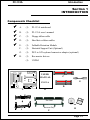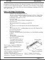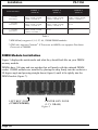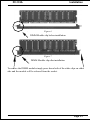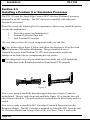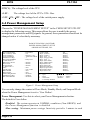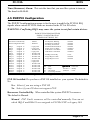
1
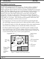
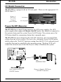
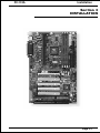
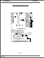
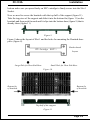
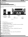
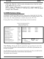
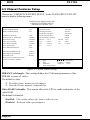
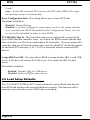
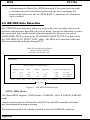
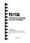
P2-133A A Pentium ® II or Deschutes Slot1 Processor based AGP mainboard (100/66MHz) TRADEMARK All products and company names are trademarks or registered trademarks of their respective holders. These specifications are subject to change without notice. Manual Revision 1.0 November 25, 1998 P2-133A P2-133A Technical Support Services If you need additional information, help during installation or normal use of this product, please contact your retailer. If your retailer can not help, you may E-Mail us with any questions at the following address [email protected] Record your serial number before installing your P2-133A mainboard. (the serial number is located near the ISA slots at the edge of the board) P2-133A serial number: __________________________ BIOS Upgrades Please use either our Web Site or BBS for current BIOS Upgrades. Internet Access http://www.epox.com http://www.epox.com.tw [email protected] [email protected] Modem Access 31-182-618451 (The Netherlands) You can access this number via a Hayes-compatible modem with a 2,400 to 28,800 baud rate. The following setup format is required: 8 Data Bits, No Parity, 1 Stop Bit. If your modem is unable to connect at higher baud rates, try connecting at 2,400 baud before contacting Technical Support. Thank you for using EPoX mainboards! © Copyright 1998 EPoX Computer Company. All rights reserved. P2-133A User Notice No part of this product, including the product and software may be reproduced, transmitted, transcribed, stored in a retrieval system, or translated into any language in any form by any means without the express written permission of EPoX Computer Company (hereinafter referred to as EPoX) except documentation kept by the purchaser for backup purposes. EPoX provides this manual “as is” without warranty of any kind, either express or implied, including but not limited to the implied warranties or conditions of merchantability or fitness for a particular purpose. In no event shall EPoX be liable for any loss or profits, loss of business, loss of use or data, interruption of business or for indirect, special incidental, or consequential damages of any kind, even if EPoX has been advised of the possibility of such damages arising from any defect or error in the manual or product. EPoX may review this manual from time to time without notice. For updated BIOS, drivers, or product release information you may visit EPoX’s home page at: http://www.epox.com Products mentioned in this manual are mentioned for identification purposes only. Product names appearing in this manual may or may not be registered trademarks or copyrights of their respective companies. The product name and revision number are both printed on the mainboard itself. Handling Procedures Static electricity can severely damage your equipment. Handle the P2-133A and any other device in your system with care and avoid unneccessary contact with system components on the mainboard. Always work on an antistatic surface to avoid possible damage to the motherboard from static discharge. We assume no responsibility for any damage to the P2-133A mainboard that results from failure to follow installation instructions or failure to observe safety precautions. CAUTION The P2-133A mainboard is subject to damage by static electricity. Always observe the handling procedures. P2-133A Table of Contents Section 1 Introduction Components Checklist .................................... 1-1 Overview Pentium II or Deschutes Processor .................. 1-2 S.E.C. Cartridge Terminology ......................... 1-3 Accelerated Graphics Port .............................. 1-4 Hardware Monitoring ..................................... 1-4 P2-133A Form-Factor ................................... 1-6 I/O Shield Connector ...................................... 1-7 Power-On/Off (Remote) ................................. 1-7 System Block Diagram ................................... 1-8 Section 2 Features P2-133A Features .......................................... 2-1 Section 3 Installation P2-133A Detailed Layout ............................... 3-2 Easy Installation Procedure Configure Jumpers .......................................... 3-3 System Memory Configuration ........................ 3-5 Installing a Pentium® II Processor .................... 3-9 Device Connectors ......................................... 3-10 External Modem Ring-in Power ON and Keyboard Power ON Function (KBPO) ........ 3-12 Section 4 Award BIOS Setup BIOS Instructions ........................................... 4-1 Standard CMOS Setup .................................. 4-2 BIOS Features Setup ..................................... 4-3 Chipset Features Setup ................................... 4-8 P2-133A Power Management Setup .............................. 4-10 PNP/PCI Configuration .................................. 4-13 Load Setup Defaults ....................................... 4-14 Integrated Peripherals ..................................... 4-15 Change Supervisor or User Password ............. 4-19 IDE HDD Auto Detection ............................... 4-20 HDD Low Level Format ................................. 4-22 Save & Exit Setup .......................................... 4-22 Exit Without Saving ......................................... 4-22 Appendix A Memory Map ................................................. A-1 I/O Map ......................................................... A-1 Timer & DMA Channels Map ......................... A-2 Interrupt Map ................................................. A-2 RTC & CMOS RAM Map ............................ A-3 Appendix B POST Codes ................................................. A-5 Unexpected Errors ......................................... A-8 Appendix C Load Setup Defaults ....................................... A-9 Appendix D CPU Clock Frequency Selection In BIOS Setting ...................................................................... A-10 P2-133A Introduction Section 1 INTRODUCTION Components Checklist ü ü ü ü ü ü A. (1) P2-133A mainboard B. (1) P2-133A user’s manual C. (1) Floppy ribbon cable D. (1) Hard drive ribbon cables E. F. (1) (1) Foldable Retention Module Heatsink Support Unit (Optional) G. (1) PS/2 to AT keyboard connector adapter (optional) H. (1) Bus master drivers (1) USDM USERS MANUAL C G P2-133A 25 26 D A B Top Half or Bottom Half E F H Page 1-1 Introduction P2-133A Overview Pentium II or Deschutes Processor The Pentium® II or Deschutes Processor (The Deschutes Processor as 300/ 100MHz, 350/100MHz, 400/100MHz and 450/100MHz speed with 512K-L2 cache Versions.) is the follow-on to the Pentium® Processor. The Pentium® II or Deschutes Processor, like the Pentium® Pro processor, implements a Dynamic Execution micro-architecture -- a unique combination of multiple branch prediction, data flow analysis, and speculative execution. This enables the Pentium® II Processor to deliver higher performance than the Pentium® processor, while maintaining binary compatibility with all previous Intel architecture processors. A significant feature of the Pentium® II or Deschutes Processor, from a system perspective, is the built-in direct multiprocessing support. In order to achieve multiprocessing, and maintain the memory and I/O bandwidth to support it, new system designs are needed. For systems with dual processors, it is important to consider the additional power burdens and signal integrity issues of supporting multiple loads on a high speed bus. The Pentium® II or Deschutes Processor card supports both uni-processor and dual processor implementations. The Pentium® II or Deschutes Processor utilizes Single Edge Contact (S.E.C.) (Figure 1) cartridge packaging technology. The S.E.C. cartridge allows the L2 cache to remain tightly coupled to the processor, while maintaining flexibility when implementing high performance processors into OEM systems. The second level cache is performance optimized and tested at the cartridge level. The S.E.C. cartridge utilizes surface mounted core components and a printed circuit board with an edge finger connection. The S.E.C. cartridge package introduced on the Pentium® II Processor will also be used in future Slot 1 processors. The S.E.C. cartridge has the following features: a thermal plate, a cover and a PCB with an edge finger connection. The thermal plate allows standardized heatsink attachment or customized thermal solutions. The thermal plate enables a reusable heatsink to minimize fit issues for serviceability, upgradeability and replacement. The full enclosure also protects the surface mount components. The edge finger connection maintains socketabilty for system configuration. The edge finger connector is denoted as ‘Slot 1 connector’ in this and other documentation. The entire enclosed product is called the Pentium® II or Deschutes Processor. The Page 1-2 P2-133A Introduction packaging technology and each of the physical elements of the product are referred to using accurate technical descriptions. This allows clear reference to the products as just a processor. This is the model used in past packaging technologies like PGA, TCP, PQFP, DIP, etc. S.E.C. Cartridge Terminology • • • • • • • • Pentium® II or Deschutes Processor The new enclosed card packaging technology is called a “Single Edge Contact cartridge.” This is similar to previous names for packaging technology such as PGA or TCP. Processor card The green PCB (with or without components on it) Processor core The silicon on the PLGA package on the PCB Cover The plastic cover on the opposite side from the thermal plate. Slot 1 The slot that the S.E.C. cartridge plugs into, just as the Pentium® Pro processor uses Socket 8. Retention mechanism Formerly ‘retention module’ the dual posts, etc. that holds the cartridge in place. Thermal plate The heatsink attachment plate. Heat sink supports The support pieces that are Thermal Plate mounted on the mainboard to provide added support for Cover heatsinks. The L2 cache (TagRAM, PBSRAM) components keep standard industry names. Processor The Pentium® II or Deschutes Processor Printed Circuit Board is the first product to utilize the S.E.C. cartridge technology and Slot 1 Figure 1: Pentium® II or Deschutes connector. Unless otherwise noted, any Processor CPU with S.E.C. Cartridge references to “Pentium® II Processor,” Page 1-3 Introduction P2-133A “Pentium® II or Deschutes Processor/Slot 1 processor” or “Deschutes Processor” will apply to both the Pentium® II Processor desktop processors. Accelerated Graphics Port (AGP or A.G.P.) Typically, 3D graphics rendering requires a tremendous amount of memory, and demands ever increasing throughput speed as well. As 3D products for the personal computer become more and more popular, these demands will only increase. This will cause a rise in costs for both end users and manufacturers. Lowering these costs as well as improving performance is the primary motivation behind AGP. By providing a massive increase in the bandwidth available between the video card and the processor, it will assist in relieving some of these pressures for quite sometime. Hardware Monitoring Hardware monitoring allows you to monitor various aspects of your systems operations and status. The features include CPU temperature, voltage and RPM of fan. Page 1-4 P2-133A Introduction Page Right Blank Page 1-5 Introduction P2-133A P2-133A Form-Factor The P2-133A is designed with ATX form factor - the latest industry standard of chassis. The ATX form factor is essentially a Baby-AT baseboard rotated 90 degrees within the chassis enclosure and a new mounting configuration for the power supply. With these changes the processor is relocated away from the expansion slots, allowing them all to hold full length add-in cards. ATX defines a double height aperture to the rear of the chassis which can be used to host a wide range of onboard I/O. Only the size and position of this aperture is defined, allowing PC manufacturers to add new I/O features (e.g.; TV input, TV output, joystick, modem, LAN, audio, etc.) to systems. This will help systems integrators differentiate their products in the marketplace, and better meet your needs. • By integrating more I/O down onto the board and better positioning the hard drive and floppy connectors material cost of cables and add-in cards is reduced. • By reducing the number of cables and components in the system, manufacturing time and inventory holding costs are reduced and reliability will increase. • By using an optimized power supply, it's possible to reduce cooling costs and lower acoustical noise. An ATX power supply, which has a side-mounted fan, allows direct cooling of the processor and add-in cards making a secondary fan or active heatsink unnecessary in most system applications. Expandable I/O ATX Power Supply Full length slots Single chassis fan for system CPU located near Power Supply 25 26 ATX power connector Floppy / IDE connectors close to peripheral bays Page 1-6 3 1/2" Bay 5 1/4" Bay Figure 2: Summary of ATX chassis features P2-133A Introduction I/O Shield Connector The P2-133A is equipped with an I/O back panel. Please use the appropriate I/O shield (figure 3). Parallel Port Figure 3: P2-133A I/O back panel layout PS/2 Mouse PS/2 Keyboard USB COM1 COM2 Power-On/Off (Remote) The P2-133A has a single 20-pin connector for ATX power supplies. For ATX power supplies that support the Remote On/Off feature, this should be connected to the systems front panel for system Power On/Off button. The systems power On/ Off button should be a momentary button that is normally open. The P2-133A has been designed with “Soft Off" functions. You can turn Off the system from one of two sources: The first is the front panel Power On/Off button, and the other is the "Soft Off" function (coming from the EP-133A’s onboard circuit controller) that can be controlled by the operating system. Windows 95/98 will control this when the user clicks that they are ready to Shutdown the system. 25 26 J3 P2-133A Board Case (chassis) Power ON/OFF button ATX POWER SUPPLY Figure 4: Simple ATX Power ON/OFF Controller Page 1-7 Introduction P2-133A System Block Diagram P e n tiu m II o r D e sc h u tes P ro ce ss o r 1 0 0 /6 6 M Hz 1 0 0 /6 6 M Hz 6 6 M Hz PC I Bridg e and m em ory controller VT8 2 C 6 9 3 VT8 2 C 5 9 6 A I/O Bridg e Winbond 8 3 9 7 7 TF Figure 5: System Block Diagram Page 1-8 P2-133A Features Section 2 FEATURES P2-133A Features: • P2-133A is based on the Pentium® II or Deschutes Processor operating at 233 ~ 333MHz (66MHz) or 300 ~ 450MHz (100MHz) on Slot 1. The board is configured by an Easy-Setting-Daul-Jumper (E.S.D.J.) to match your CPU clock speed. • Designed with VIA APOLLO PRO+ 693/596A AGPset. • Supports up to 384 Mega of DRAM (minimum of 16 MB) on board, You can use 168-pin DIMM x 3. It will automatically detect Extended Data Output (EDO) DRAM at 66MHz only or Synchronous DRAM memory (SDRAM) at 66MHz or 100MHz (please see Section 3-2). • P2-133A will support Error Checking and Correcting (ECC) when using paritys DRAM memory modules. This will detect multiple bit errors and correct 1-bit memory errors. • Supports (2) 16 bit ISA slots, (5) 32 bit PCI slots, (1) AGP slot and provides (2) independent high performance PCI IDE interfaces capable of supporting PIO Mode 3/4 and Ultra DMA 33 devices. The P2-133A supports (5) PCI Bus Master slots and a jumperless PCI INT# control scheme which reduces configuration confusion when plugging in PCI card(s). • Supports ATAPI (e.g. CD-ROM) devices on both Primary and Secondary IDE interfaces. • Designed with Winbond W83977TF Multi I/O: (1) floppy port, (1) parallel port (EPP, ECP), and (2) serial ports (16550 Fast UART). Note: Japanese “Floppy 3 mode” is also supported • Includes a PS/2 mouse connector. • Allows use of a PS/2 keyboard. • Features Award Plug & Play BIOS. With Flash Memory you can always upgrade to the current BIOS as they are released. (http://www.epox.com please visit our Technical Support section for the latest updates) Page 2-1 Features P2-133A • P2-133A utilizes a Lithium battery which provides environmental protection and longer battery life. • Supports the Universal Serial Bus (USB) connector. The VIA 82C596A chip provides the means for connecting PC peripherals such as; keyboards, joysticks, telephones, and modems. • Built-in ATX 20-pin power supply connector. • Software power-down when using Windows® 95/98. • Supports ring-in feature (remote power-on through external modem, allows system to be turned on remotely. • Resume by Alarm - Allows your system to turn on at a preselected time. • Power Loss Recovery - In the event of a power outtage your system will automatically turn itself back on without user intervention. • Supports CPU Hardware sleep and SMM (System Management Mode). • Supports Desktop Management Interface (DMI) facilitating the management of desktop computers, hardware and software components and peripherals, whether they are stand-alone systems or linked into networks. (optional) • Supports Hot key, Any key or password Keyboard power ON function (KBPO). • Supports USDM software to offer motherboard various status on Windows® 95/98, or Windows® NT 4.0/5.0. • Supports the CPU, PWR and Chassis fan Auto stop in sleep mode. • Supports the System Power LED (PANEL) blinks in the sleep mode. • Built-in WOL (Wake On Lan) Connector. • Built-in SB-LINK Header for Creative Blaster® AWE64D PCI Bus Sound Card. Page 2-2 P2-133A Installation Section 3 INSTALLATION Page 3-1 Installation P2-133A Bank 2 J5 ATX Power Input Keyboard (Bottom) JP13 DIMM 1 DIMM 2 DIMM 3 USB 0 CPU Cartridge SLOT 1 (Top) J3 FDD1 USB 1 + IR CONN. 1 5 KEYLOCK 1 SPK RESET IDE2 IDE1 PCI Slot #1 PCI Slot #2 Battery J8 SB_Link PCI Slot #4 PCI Slot #5 ISA Slot #1 ISA Slot #2 Figure 1 Page 3-2 1 JP1 JP3 1 2 ESDJ Flash Memory for BIOS PCI Slot #3 J6 CHASSIS FAN Winbond 83977 I/Oset AGP SLOT J7:WOL 25 26 POWER_ON + Secondary IDE (Bottom) Parallel Port COM 2 COM 1 USB POWER FAN J4 (Top) PS/2 Bank 1 CPU FAN Mouse Bank 0 P2-133A Detailed Layout 3X 3.5X 4X 4.5X 5X 5.5X AUTO 66MHz 100MHz 103MHz 112MHz 124MHz 133MHz J2 P2-133A Installation Easy Installation Procedure Easy Installation Procedure The following must be completed before powering on your new system: 3-1. 3-2. 3-3. 3-4. Configure Jumpers to match your hardware Install memory chips Install Pentium II or Deschutes Processor Device Connectors Section 3-1 Configure Jumpers We design this mainboards with an ESDJ to make your installation fast and easy. The following will describe all of the ESDJ that you are required to set before moving on to step 3-2. Note: The ESDJ as depicted as shown (Figure 1) in their correct physical orientation. JP 1 1 3 JP 13 1 3 C M O S C lea r JP 1 = 1 -2 - R u n M o d e (D e fa u lt) = 2 -3 - C le a r C M O S (m o m e n ta r ily ) K e y b o a r d P o w e r -O N fu n ctio n (re fe r th e s ec tio n 3 -5 ) JP 13 = 1 -2 - E n a b le d = 2 -3 - D is a b le d (D e fa u lt) J7 W O L (W a k u p O n L a n ) C o n n e c to r R e s e rv ed fo r N I C (N e tw o r k In te rfa c e C a r d ) to W a k e th e S y s te m . J8 S B -L I N K H ea d e r R e s e rv ed fo r C r e a tiv e S B -L I N K (S o u n d B la s te r L IN K ) w ith th e S o u n d B la ste r AW E 6 4 D P C I S o u n d C a r d to C o m p a tib le D O S g a m e s a n d M u ltim e d ia a p p lica tio n s. T M T M Page 3-3 Installation P2-133A * * * * * ** Note: Based on the implementation of VIA Chipset Apollo Pro+, P2-133A is able to provide two host bus frequencies -- either 66 or 100MHz for Slot1 processor and memory operating. The default is set at 100MHz once Pentium® II processor to be mounted onto this mainboard. However, no matter what kind of Slot1 processor you installed, it should come with right memory modules for normal and stable operation. For example, if you install a Deschutes processor, you should use the SDRAM module with 100MHz based(or above) to match the CPU speed. Furthermore, one thing you may need to bear in mind, before the CPU installation, it is anyway our advice to use JP3 and set up right speed of Slot1 processor at any time. Page 3-4 P2-133A Installation Section 3-2 System Memory Configuration Memory Layout The P2-133A supports (3) 168-pin DIMMs (Dual In-line Memory Module). The DIMMs can be either EDO (Extended Data Out) or SDRAM (Synchronized DRAM). The DIMMs may be installed using just one chip. • • • We recommend using SDRAM DIMM can not mixing with EDO DIMM modules. The EDO DIMM only support pentium® II Processor at 66MHz, not support Deschutes Processor at 100MHz. We recommend when installed the 100MHz Deschutes Processor using DIMM SDRAM must be 125MHz (-8ns) bus speed. If used 100MHz (-10ns) SDRAM may be critical timing for the motherboard. • About the “PC/100 SDRAM spec.” information you may visit Intel’s home page at: http//developer.intel.com/design/pcisets/memory/index.htm • DIMM SDRAM may be 83MHz (-12ns), 100MHz (-10ns) or 125MHz (-8ns) bus speed. Figure 2 and Table 1 show several possible memory configurations using DIM M 1 (M 1 ) B ank 0 DIM M 2 (M 2 ) B ank 1 DIM M 3 (M 3 ) B ank 2 -S y n ch ro n o u s -S D R A M o r E D O D IM M F igu re 2 Page 3-5 Installation P2-133A D IM M 1 (B ank 0) Total M e mory D IM M 2 (B ank 1) D IM M 3 (B ank 2) = 384MB Maximum EDO /SDRAM* 8MB, 16MB, 32MB, 64MB, 128MB X 1 EDO /SDRAM* 8MB, 16MB, 32MB, 64MB, 128MB X 1 EDO /SDRAM* 8MB, 16MB, 32MB, 64MB, 128MBX 1 = 256MB Maximum EDO /SDRAM* 8MB, 16MB, 32MB, 64MB, 128MB X 1 EDO /SDRAM* 8MB, 16MB, 32MB, 64MB, 128MB X 1 N one = 128MB Maximum EDO /SDRAM* 8MB, 16MB, 32MB, 64MB, 128MBX 1 N one N one Table 1 * SDRAM only supports 8, 16, 32, 64, 128MB DIMM modules. * EDO only supports Pentium® II Processor at 66MHz, not supports Deschutes Processor at 100MHz. DIMM Module Installation Figure 3 displays the notch marks and what they should look like on your DIMM memory module. DIMMs have 168-pins and two notches that will match with the onboard DIMM socket. DIMM modules are installed by placing the chip firmly into the socket at a 90 degree angle and pressing straight down (figure 6) until it fits tightly into the DIMM socket (figure 7). LEFT KEY ZONE (UNBUFFERED) CENTER KEY ZONE (3.3 V DRAM) Figure 3 Page 3-6 P2-133A Installation Figure 6 DIMM Module clip before installation Figure 7 DIMM Module clip after installation To remove the DIMM module simply press down both of the white clips on either side and the module will be released from the socket. Page 3-7 Installation P2-133A Section 3-3 Installing a Pentium II or Deschutes Processor The P2-133A uses the Single Edge Contact (SEC) slot for a Pentium II processor packaged in an SEC cartridge. The SEC slot is not compatible with other nonPentium II processors. Please have ready the following list of components so that we may install the processor onto the motherboard. 1. 2. 3. Heat sink support (top/bottom piece) Pentium II processor heat sink Intel Pentium II Processor OK, now that you have all of your components ready, we can start. First, please refer to figure 8 below, and follow the direction to lift up the fixed foldable pentium® II Retention Mechanism. This pre-installed device is designed for you to install Pentium® II CPU more easier and to avoide any damage on the board due to overtightening the four screws. One thing must be kept in your mind that please make sure to lift upright the foldable parts of the Retention module to fit and install CPU properly. Figure 8 Now we are going to install the heatsink support base piece (figure 9) onto the motherboard. There is both a large and small hole (figure 10) so that the base will only fit in one direction. This piece needs to be pushed into the holes firmly until it is seated. Now we are ready to install the SEC Cartridge (Pentium II Processor) into the Retention Module. The SEC Cartridge is mounted by sliding the SEC Cartridge into the Retention Module and letting it slide all the way down. Once it reaches the Page 3-8 P2-133A Installation bottom make sure you press firmly on SEC cartridge to firmly secure into the Slot 1 Socket. Now we need to secure the heatsink with the top half of the support (figure 11). Take the top piece of the support and slide it into the bottom fin (figure 11) on the heatsink and then push forward until it clips into the bottom base (figure 9) that is already there (figure 11). Figure 9 Figure 9 shows the layout of Slot 1 and the holes for mounting the Heatsink base piece (figure 8). Motherboard CPU Car tr idge SLOT 1 Large Hole for Heat Sink Base Layout Small Hole for Heat Sink Base Figure 10 Bottom fin of heatsink Bottom fin of heatsink Top half of the support Figure 11 Page 3-9 Installation P2-133A Section 3-4 Device Connectors Please install the motherboard into the chassis. Now that your motherboard is installed you are ready to connect all your connections (figure 12). 12345678901234567890123456789012123456789012345678901234567890121234567890123456789012345 12345678901234567890123456789012123456789012345678901234567890121234567890123456789012345 PS/2 Mouse (Top) PS/2 Keyboard (Bottom) USB 1 (Top) USB 0 (Bottom) Parallel Port (Top) Com1 (Bottom Left) Figure 12 J4: Com2 (Bottom Right) CPU Fan Power • A plug-in for the CPU Fan Power J5: Power Supply Fan Monitoring • A plug-in for the Power supply so that BIOS can monitor the RPM’s J6: Chassis Fan Power • A plug-in for the chassis Fan Power J7: WOL (Wake On Lan) Connector J8: SB-LINK Connector • 5-PIN Header for Creative Blaster® AWE64D PCI Sound Card. PW2: ATX Power Connector • 20-pin power connector J2,J3:Chassis Panel Connector • Keylock, Speaker, Reset, Sleep, Turbo LED and HDD LED IDE1:Primary IDE Connector IDE2:Secondary IDE Connector FDD1:Floppy Controller Connector Page 3-10 P2-133A Installation Section 3-4 Device Connectors (continued) 1 Reset - Closed to restart system. J2 Speaker - Connect to the system's speaker for beeping 1. Speaker 3. GND 2. N/C 4. GND KeyLock - Keyboard lock switch & Power LED connector 1. Power LED(+) 4. Keylock 2. N/C 5. GND * The power LED lights when the 3. GND system is powered on and blinks in SLEEP MODE (Suspend mode). 1 IR Connector 1. VCC 2. NC 3. IRRX J3 + + 4. GND 5. IRTX IDE LED indicator - LED ON when Onboard PCI IDE Hard disks is activate Turbo LED indicator - LED ON when higher speed is selected Power On/Off - This is connected to the power button on the case. Using the Soft-Off by Pwr-BTTN feature, you can choose either Instant Off (turns system off immediatly), or 4 sec delay (you need to hold the button down for 4 seconds before the system turns off). When the system is in 4 sec delay mode, we has added a special feature to make the system go into suspend mode when the button is pressed momentarily. Page 3-11 Installation P2-133A Section 3-5 External Modem Ring-in Power ON and Keyboard Power ON Functions (KBPO) On the basis of bounded functions in I/O chipset, the two serial ports are able to support the External Modem Ring-in Power ON function. Once users connect the external modem to COM1 or COM2, the P2-133A mainboard allows users to turn on their system through the remote and host's dial-up control. Exclusive Keyboard Power ON Function To innovate a unique feature to benefit users, we devoted the easiest and most convenient way to turn on your system based on the the ATX power supply. How to work with it Step 1:Please check JP13 at the position 1-2 after you finished the system installation. JP13 K eybo a rd P ow er-O N F un ctio n Se le ctio n 1 -2 : E n ab led 2 -3 : D isab led (D efau lt) Step 2:Push the momentary switch (J3 PW-ON) to turn on your system and then push again to hold for more than 4 seconds to turn it off affter counted memory as soon as you turn it on. Step 3:You can enjoy the Keyboard Power ON function (KBPO) by pressing any 1 key, Hot key (Ctrl-F1, F2.....F12), Password (A maximum of 5 characters can be entered.) and BUTTON only to turn on your system. Please refer to the BIOS Integrated peripherals setup for detail (Page 4-23). The BIOS Default is keyboard Hot key <Ctrl> - <F1> to turn on the system. Your system will be turned on automatically, after releasing the keys. To power off you system, you can use the Soft-OFF function under Windows95 Page 3-12 P2-133A Installation Notes: 1.Intel ATX version 2.0 specification has recommended you use the power supply with 0.72A(720mA) in 5.0VSB. With our P2-133A mainboard, the 5.0VSB standby power only has to be > = 0.1A (100mA) then you can enjoy this unique benefit. However, the ATX power supply which is < 0.1 (100mA) is still applicable to your system by placed JP13 at the position 2-3 to disable this feature. Page 3-13 Installation P2-133A Page Left Blank Page 3-14 P2-133A BIOS Section 4 AWARD BIOS SETUP BIOS Instructions Award’s ROM BIOS provides a built-in Setup program which allows user to modify the basic system configuration and hardware parameters. The modified data will be stored in a battery-backed CMOS, so that data will be retained even when the power is turned off. In general, the information saved in the CMOS RAM will stay unchanged unless there is a configuration change in the system, such as hard drive replacement or a device is added. It is possible for the CMOS battery to fail, this will cause data loss in the CMOS only. If this does happen you will need to reconfigure your BIOS settings. To enter the Setup Program : Power on the computer and press the <Del> key immediately, this will bring you into the BIOS CMOS SETUP UTILITY. ROM PCI / ISA BIOS (2A6LFPAB) CMOS SETUP UTILITY AWARD SOFTWARE, INC. STANDARD CMOS SETUP SUPERVISOR PASSWORD BIOS FEATURES SETUP USER PASSWORD CHIPSET FEATURES SETUP IDE HDD AUTO DETECTION POWER MANAGEMENT SETUP HDD LOW LEVEL FORMAT PNP/PCI CONFIGURATION SAVE & EXIT SETUP INTEGRATED PERIPHERALS EXIT WITHOUT SAVING LOAD SETUP DEFAULTS ESC : QUIT F10 : Save & Exit Setup é ê è ç : SELECT ITEM (Shift)F2 : Change Color Time, Date, Hard Disk Type... Figure 1: CMOS Setup Utility Page 4-1 BIOS P2-133A The menu displays all the major selection items. Select the item you need to reconfigure. The selection is made by moving the cursor (press any direction key ) to the item and pressing the ‘Enter’ key. An on-line help message is displayed at the bottom of the screen as the cursor is moved to various items which provides a better understanding of each function. When a selection is made, the menu of the selected item will appear so that the user can modify associated configuration parameters. 4-1 Standard CMOS Setup Choose “Standard CMOS Setup” in the CMOS SETUP UTILITY Menu (Figure 2). The Standard CMOS Setup allows the user to configure system settings such as the current date and time, type of hard disk drive installed, floppy drive type, and display type. Memory size is auto-detected by the BIOS and displayed for your reference. When a field is highlighted (use direction keys to move the cursor and the <Enter> key to select), the entries in the field can be changed by pressing the <PgDn> or the <PgUp> key. ROM PCI/ISA BIOS(2A6LFPAB) STANDARD CMOS SETUP AWARD SOFTWARE, INC. Date (mm:dd:yy) : Wed, Apr 17 1996 Time (hh:mm:ss) : 14 : 30 : 50 HARD DISKS TYPE Primary Master : Auto Primary Slave : Auto Secondary Master : Auto Secondary Slave : Auto SIZE 0 0 0 0 CYLS 0 0 0 0 HEAD 0 0 0 0 Drive A : 1.44M, 3.5 in. Drive B : None Floppy 3 Mode Support : Disabled Video : EGA/VGA Halt On : All, But Keyboard ESC : Quit F1 : Help PRECOMP 0 0 0 0 SECTORS MODE 0 Auto 0 Auto 0 Auto 0 Auto Base Memory Extended Memory Other Memory : : : 640K 64512K 384K Total Memory : 65536K é ê è ç : Select Item (Shift) F2 LANDZONE 0 0 0 0 PU/PD/+/- : Modify : Change Color Figure 2: Standard CMOS Setup NOTE: If the hard disk Primary Master/Slave and Secondary Master/Slave are set to Auto, then the hard disk size and model will be auto-detected. Page 4-2 P2-133A BIOS NOTE: The “Halt On:” field is used to determine when to halt the system by the BIOS if an error occurs. NOTE: Floppy 3 Mode support is a mode used to support a special 3.5” drive used in Japan. This is a 3.5” disk that stores only 1.2 MB, the default setting for this is disabled. 4-2 BIOS Features Setup Selecting the “BIOS FEATURES SETUP” option in the CMOS SETUP UTILITY menu allows users to change system related parameters in the displayed menu. This menu shows all of the manufacturer’s default values for the P2-133A. Pressing the [F1] key will display a help message for the selected item. ROM PCI/ISA BIOS(2A6LFPAB) BIOS FEATURES SETUP AWARD SOFTWARE, INC. Virus Warning CPU Internal Cache External Cache CPU L2 Cache ECC Checking Quick Power On Self Test Boot Sequence Swap Floppy Drive Boot Up Floppy Seek Boot Up NumLock Status Gate A20 option Memory Parity/ECC Check Typematic Rate Setting Typematic Rate (Chars/Sec) Type matic Delay (Msec) Security Option PCI/VGA Palette Snoop OS Select For DRAM > 64MB Report NO FDD For Win 95 : Disabled : Enabled : Enabled : Disabled : Enabled : A, C, SCSI : Disable : Enabled : On : Fast : Disabled : Disabled :6 : 250 : Setup : Disabled : Non-OS2 : Yes Video BIOS C8000-CBFFF CC000-CFFFF D0000-D3FFF D4000-D7FFF D8000-DBFFF DC000-DFFFF Esc F1 F5 F7 : : : : Shadow Shadow Shadow Shadow Shadow Shadow Shadow Quit Help Old Values Load Setup Defaults : Enabled : Disabled : Disabled : Disabled : Disabled : Disabled : Disabled é ê è ç : Select Item PU/PD/+/- : Modify (Shift) F2 : Color Figure 3: BIOS Features Setup Virus Warning: During and after the system boots up, any attempt to write to the boot sector or partition table of the hard disk drive will halt the system and an error message will appear. You should then run an anti-virus program to locate the virus. Keep in mind that this feature protects only the boot sector, not the entire hard drive. The default value is Disabled. Page 4-3 BIOS P2-133A Enabled: Activates automatically when the system boots up causing a warning message to appear when anything attempts to access the boot sector. Disabled: No warning message will appear when anything attempts to access the boot sector. Note: Many disk diagnostic programs that access the boot sector table can trigger the virus warning message. If you plan to run such a program, we recommend that you first disable the virus warning. CPU Internal Cache: This controls the status of the processor’s internal cache area. The default is Enabled. Enabled: This activates the processor’s internal cache thereby increasing performance. Disabled: This deactivates the processor’s internal cache thereby lowering performance. CPU L2 Cache ECC Checking: This controls the CPU’s L2 cache to supports Error Checking and Correcting(ECC). The default is Disabled Enabled: Enabled the CPU’s L2 cache to Support ECC function. When enabled this item the performance should be impact 2% ~4%. Disabled: Disabled the CPU’s L2 cache to support ECC function. External (L2) Cache: This controls the status of the external (L2) cache area. The default is Enabled. Enabled: This activates the motherboard’s L2 cache thereby increasing performance. Disabled: This deactivates the motherboard’s L2 cache thereby lowering performance. Quick Power On Self Test: This category speeds up the Power On Self Test (POST). The default is Enabled. Enabled: This setting will shorten or skip of the items checked during POST. Disabled: Normal POST. Page 4-4 P2-133A BIOS Boot Sequence: This category determines which drive is searched first by the O/S (Operating System). The default is A,C,SCSI. The following is your list of options: [A, C, SCSI] - [C, A, SCSI] - [C, CD-ROM, A] - [CD-ROM, C, A] [D, A,CD-ROM],[E, A, CD-ROM] - [F, A, CD-ROM] - [SCSI, A, C] [SCSI C, A] - [C Only] Swap Floppy Drive: This will swap your physical drive letters A & B if you are using two floppy disks. The default is Disabled. Enabled: Floppy A & B will be swapped under the O/S. Disabled: Floppy A & B will be not swapped. Boot Up Floppy Seek: During Power-On-Self-Test (POST), BIOS will determine if the floppy disk drive installed is 40 or 80 tracks. Only 360K type is 40 tracks while 760K, 1.2MB and 1.44MB are all 80 tracks. The default is Enabled. Enabled: The BIOS will search the floppy disk drive to determine if it is 40 or 80 tracks. Disabled: The BIOS will not search for the type of floppy disk drive by track number. NOTE: BIOS can not tell the difference between 720K, 1.2MB and 1. 44MB drive types as they are all 80 tracks. Boot Up NumLock Status: This controls the state of the NumLock key when the system boots. The default is On. On: The keypad acts as a 10-key pad. Off: The keypad acts like the cursor keys. Gate A20 Option: This refers to the way the system addresses memory above 1MB (extended memory). The default is Fast. Normal: The A20 signal is controlled by the keyboard controller or chipset Page 4-5 BIOS P2-133A hardware. Fast: The A20 signal is controlled by Port 92 or chipset specific method. Typematic Rate Setting: This determines the keystrokes repeat rate. The default is Disabled. Enabled: Allows typematic rate and typematic delay programming. Disabled: The typematic rate and typematic delay will be controlled by the keyboard controller in your system. Typematic Rate (Chars/Sec): This is the number of characters that will be repeated by a keyboard press. The default is 6. 6: 6 characters per second. 10: 10 characters per second. 15: 15 characters per second. 24: 24 characters per second. 8: 8 characters per second. 12: 12 characters per second. 20: 20 characters per second. 30: 30 characters per second. Typematic Delay (msec): This setting controls the time between the first and the second character displayed by typematic auto-repeat. The default is 250. 250: 250 msec. 500: 500 msec. 750: 750 msec. 1000: 1000 msec. Security Option: This category allows you to limit access to the System and Setup, or just to Setup. The default is Setup. System: The system will not boot and the access to Setup will be denied if the correct password is not entered at the prompt. Setup: The system will boot; but the access to Setup will be denied if the incorrect password is not entered at the prompt. PCI/VGA Palette Snoop: This field controls the ability of a primary PCI VGA controller to share a common palette (When a snoop write cycles) with an ISA video card. The default is Disabled. Enabled: If an ISA card is connected to a PCI VGA card via the VESA connector, and that ISA card connects to a VGA monitor, then that ISA card Page 4-6 P2-133A BIOS uses the RAMDAC of the PCI card. Disabled: Disables the VGA card Palette Snoop function. OS Select For DRAM > 64MB: Some operating systems require special handling. Use this option only if your system has greater than 64MB of memory. The default is Non-OS2. OS2: Select this if you are running the OS/2 operating system with greater than 64MB of RAM. Non-OS2: Select this for all other operating systems and configurations. Report No FDD For WIN95: This option allows BIOS to indicate whether WIN95 is with FDD or not. The Default value is Yes. NO: Report No FDD for WIN95. YES: Report FDD for WIN95 Video BIOS Shadow: This option allows video BIOS to be copied into RAM. Video Shadowing will increase the video performance of your system. The default is Enabled. Enabled: Video shadow is enabled. Disabled: Video shadow is disabled. C8000 - CBFFF Shadow: CC000 - CFFFF Shadow: D0000 - D3FFF Shadow: D4000 - D7FFF Shadow: D8000 - DBFFF Shadow: DC000 - DFFFF Shadow: These categories determine whether ROMs from option cards will be copied into RAM. This will be in 16K byte or 32K byte units, and the size will depend on chipset of the option card. Enabled: Optional shadow is enabled. Disabled: Optional shadow is disabled. Page 4-7 BIOS P2-133A 4-3 Chipset Features Setup Choose the “CHIPSET FEATURES SETUP” in the CMOS SETUP UTILITY menu to display following menu. ROM PCI/ISA BIOS(2A6LFPAB) CHIPSET FEATURES SETUP AWARD SOFTWARE, INC. Bank 0/1 DRAM Timing Bank 2/3 DRAM Timing Bank 4/5 DRAM Timing : Fast : Fast : Fast SDRAM Cycle length Memory Hole At 15Mb Addr. Read Around write Concurrent PCI/Host Video RAM Cacheable AGP Aperture Size Delay DRAM Read Latch : Auto : Disabled : Disabled : Enabled : Disabled : 64M : 2.0ns Auto Detect DIMM/PCI Clk Spread Spectrum Modulated CPU Host Clock Press<Ins> Key while Power-On if system can not boot normally. : Enabled : Enabled : Default System/CPU Warning Temp. Current CPU Temp. Current System Temp. Current CPU Fan Speed Current CPU Fan Speed Current Chasiss Fan Speed CPUcore :2.76 V +3.3V : 3.28 V +12V : 12.09 V -5V : -5.07 V Esc F1 F5 F7 : : : : Quit Help Old Values Load Setup Defaults : 50°C/122° : 39°C/102° : 29°C/84° : 4272 RPM : 0 RPM : 0 RPM CPUI/O : 1.47 V +5V : 4.89 V -12V : -11.98 V é ê è ç : Select Item PU/PD/+/- : Modify (Shift) F2 : Color Figure 4: Chipset Features Setup SDRAM Cycle length: This setting defines the CAS timing parameter of the SDRAM in terms of clocks. The default is Auto. 2: Provides faster memory performance. 3: Provides better memory compatibility. Video RAM Cacheable: This option allows the CPU to cache read/writes of the video RAM. The default is Enabled. Enabled: This option allows for faster video access. Disabled: Reduced video performance. Page 4-8 P2-133A BIOS Memory Hole at 15M-16M: You can reserve this memory area for the use of ISA adaptor ROMs. The default is Disabled. Enabled: This field enables the main memory (15~16MB) to remap to ISA BUS. Disabled: Normal Setting. NOTE: If this feature is enabled you will not be able to cache this memory segment. AGP Aperture Size: The amount of system memory that the AGP card is allowed to share. The default is 64. 4: 4MB of systems memory accessable by the AGP card. 8: 8MB of systems memory accessable by the AGP card. 16: 16MB of systems memory accessable by the AGP card. 32: 32MB of systems memory accessable by the AGP card. 64: 64MB of systems memory accessable by the AGP card. 128: 128MB of systems memory accessable by the AGP card. 256: 256MB of systems memory accessable by the AGP card. Auto Detect DIMM/PCI Clk: Allows you to stop DIMM/PCI Clock drive when the DIMM site or PCI Slot are not plug. This item may help reduce EMI. The default is Enabled. Enabled: Provides unused DIMM/PCI to stop. Disabled: Provides the clock generator always driving. Spread Spectrum Modulated: Allows you to active the Spread Spectrum Modulation function for reduce EMI. (Note: When Enabled the item that performance will be impacted). The default is Enabled. Enabled: Provides the Spread Spectrum function from clock generator. Disabled: NO Spread Spectrum function. Current CPU Temperature: This is the current temperature of the CPU. Current Power FAN Speed: The current power fan speed in RPMs. Current CPU FAN Speed: The current CPU fan speed in RPMs. Current Chassis FAN Speed: The current chassis fan speed in RPMs. Page 4-9 BIOS P2-133A CPU(V): The voltage level of the CPU. +1.5V: The voltage level of the CPU’s GTL+ Bus. +3.3V, +5V, +12V: The voltage level of the switch power supply. 4-4 Power Management Setup Choose the “POWER MANAGEMENT SETUP” in the CMOS SETUP UTILITY to display the following screen. This menu allows the user to modify the power management parameters and IRQ signals. In general, these parameters should not be changed unless it’s absolutely necessary. ROM PCI/ISA BIOS (2A6LFPAB) POWER MANAGEMENT SETUP AWARD SOFTWARE, INC. Power Management PM Control by APM Video off Option Video off Method MODEM Use IRQ Soft-off by PWRBTN ** RM Timers ** HDD Power Down Doze Mode Suspend Mode ** RM Events ** VGA LPT & COM HDD & FDD DMA /master Modem Ring Resume MODEM Use IRQ RTC Alarm Resume : User Define : Yes : Suspend -> Off : V/H SYNC+Blank :3 : Delay 4 Sec : Disable : Disable : Disable : OFF : LPT /COM : OFF : OFF : Disabled : Enabled : Disabled Primary INTR IRQ3 (COM 2) IRQ4 (COM 1) IRQ5 (LPT 2) IRQ6 (Floppy Disk) IRQ7 (LPT 1) IRQ8 (RTC Alarm) IRQ9 (IRQ2 Redir) IRQ10(Reserved) IRQ11(Reserved) IRQ12(PS/2 Mouse) IRQ13(Coprocessor) IRQ14(Hard Disk) IRQ15(Reserved) Esc F1 F5 F7 : : : : Quit Help Old Values Load Setup Defaults : ON : Primary : Primary : Primary : Disabled : Primary : Disabled : Primary : Primary : Primary : Primary : Primary : Primary : Disabled é ê è ç : Select Item PU/PD/+/- : Modify (Shift) F2 : Color Figure 5: Power Management Setup You can only change the content of Doze Mode, Standby Mode, and Suspend Mode when the Power Management is set to ‘User Define’. Power Management: Use this to select your Power Management selection. The default is User define. Disabled: The system operates in NORMAL conditions (Non-GREEN), and the Power Management function is disabled. Max. saving: Maximum power savings. Inactivity period is 1 minute in each Page 4-10 P2-133A BIOS mode. Min. saving: Minimum power savings. Inactivity period is 1 hour in each mode. User define: Allows user to define PM Timers parameters to control power saving mode. PM controlled APM: This option shows whether or not you want the Power Management to be controlled the Advanced Power Management (APM). The default is Yes. Yes: APM controls your PM No: APM does not control your PM Video Off Method: This option allows you to select how the video will be disabled by the power management. The default is V/H Sync + Blank V/H Sync + Blank: System turns off vertical and horizontal synchronization ports and writes blanks to the video buffer. DPMS: Select this option if your monitor supports the Display Power Management Signaling (DPMS) standard of the Video Electronics Standards Association (VESA). Use the software supplied for your video subsystem to select video power management values. Blank Screen: System only writes blanks to the video buffer. Video Off option: Tells you what time frame that the video will be disabled under current power management settings. The default is Standby. Standby: Video powers off after time shown in standby mode setting. Doze: Video powers off after time shown in doze mode setting. Suspend: Video powers off after time shown in suspend mode setting. N/A: Video power off not controlled by power management. MODEM Use IRQ: Name the interrupt request (IRQ) line assigned to the modem (if any) on your system. Activity of the selected IRQ always awakens the system. Default is IRQ 3. N/A: No IRQ is used. 4: IRQ 4 7: IRQ 7 10: IRQ 10 3: IRQ 3 5: IRQ 5 9: IRQ 9 11: IRQ 11 Page 4-11 BIOS P2-133A The P2-133A supports HDD Power Down, Doze and Standby power saving functions when using the Intel Pentium II Processor. The default is Disabled Doze Mode: The “Doze” mode timer starts to count when no “PM events” have occurred. Suspend Mode: This function works only when the Pentium II Processor is installed. The timer starts to count when “System Standby” mode timer is timed out and no “PM Events” are occurring. Valid range is from 1 minute up to 1 hour. HDD Power Down: HDD Standby timer can be set from 1 to 15 minute(s). VGA Active Monitor: Use this option if your monitor has advanced power saving features. The default is Enabled Enabled: Your monitor’s power features will be included in power management. Disabled: Your monitor’s power features will not be included in power management. Soft-Off by PWR-BTTN: Use this to select your soft-off function. The default is Delay 4 sec. Instant Off: Turns off instantly. Delay 4 Second : Turns off after a 4 second delay. If momentary press of button, the system will go into Suspend Mode. Press again to take system out of Suspend Mode. Resume by Alarm: This option allows you to have the system turn on at a preset time each day or on a certain day. This option is only available when Power Loss Recovery is Enabled. The default is Enabled. Enabled: The system will turn on at the preset time. Disabled: The system will not turn on until you turn it on. Date (of month) Alarm: This is how you set the date that the system will turn on. The default is 0. 0: Setting this to 0 will turn the system on everyday at the preset time. 1-31: Represents the day of the month that you need the system to turn on. Page 4-12 P2-133A BIOS Time (hh:mm:ss) Alarm: This sets the time that you need the system to turn on. The deault is 08:00:00. 4-5 PNP/PCI Configuration The PNP/PCI configuration program is for the user to modify the PCI/ISA IRQ signals when various PCI/ISA cards are inserted in the PCI or ISA slots. WARNING: Conflicting IRQ’s may cause the system to not find certain devices. ROM PCI/ISA BIOS(2A6LFPAB) PNP/PCI CONFIGURATION AWARD SOFTWARE, INC. PNP OS Installed Resources Controlled By Reset Configuration Data : No : Manual : Disabled IRQ-3 IRQ-4 IRQ-5 IRQ-7 IRQ-9 IRQ-10 IRQ-11 IRQ-12 IRQ-14 IRQ-15 DMA-0 DMA-1 DMA-3 DMA-5 DMA-6 DMA-7 : : : : : : : : : : : : : : : : assigned assigned assigned assigned assigned assigned assigned assigned assigned assigned assigned assigned assigned assigned assigned assigned to to to to to to to to to to to to to to to to Legacy ISA Legacy ISA PCI/ISA PnP Legacy ISA PCI/ISA PnP PCI/ISA PnP PCI/ISA PnP PCI/ISA PnP Legacy ISA Legacy ISA PCI/ISA PnP PCI/ISA PnP PCI/ISA PnP PCI/ISA PnP PCI/ISA PnP PCI/ISA PnP CPU to PCI Write Buffer PCI Dynamic Bursting PCI Master 0 WS Write PCI Delay Transaction PCI Master Read Prefetch PCI#2 Access #1 Retry AGP Master 1 WS Write AGP Master 1 WS Read : Enabled : Enabled : Enabled : Enabled : Enabled : Disabled : Enabled : Disabled PCI IRQ Actived By Assign IRQ For USB Assign IRQ For VGA : Level : Enabled : Enabled Esc F1 F5 F7 : : : : Quit Help Old Values Load Setup Defaults é ê è ç : Select Item PU/PD/+/- : Modify (Shift) F2 : Color Figure 6: PCI Configuration Setup PNP OS Installed: Do you have a PNP OS installed on your system. The default is No. Yes: Select if you are using a PNP OS No: Select if your OS does not support PNP. Resources Controlled By: Who controlled the system PNP/PCI resources. The default is Manual. Manual: PNP Card’s resources will be controlled manually. You can set which IRQ-X and DMA-X are assigned to PCI/ISA PNP or Legacy ISA Page 4-13 BIOS P2-133A Cards. Auto: If your ISA card and PCI card are all PNP cards, BIOS will assign the interrupt resource automatically. Reset Configuration Data: This setting allows you to clear ESCD data. The default is Disabled Disabled: Normal Setting. Enabled: If you have plugged in some Legacy cards to the system and they were recorded into ESCD (Extended System Configuration Data), you can set this field to Enabled in order to clear ESCD. PCI IDE IRQ Map To: This item allows the user to configure the system for the type of IDE hard disk controller in use. By default, the BIOS assumes that the hard drive controller is an ISA device rather than a PCI controller. If you are using a PCI controller, then you will need to change this to specify which PCI slot has the controller and which PCI interrupt (A, B, C, or D) is associated with the connected IDE devices. Assign IRQ For USB: This item allows BIOS to assign whether IRQ is with USB or not. If you have not connect the USB device. Can release the IRQ for other device. The default is Enabled. Enalbed: Provides IRQ for USB device. Disabled: Release IRQ for other device. 4-6 Load Setup Defaults The “LOAD SETUP DEFAULTS” function loads the system default data directly from ROM and initializes the associated hardware properly. This function will be necessary only when the system CMOS data is corrupted. Page 4-14 P2-133A BIOS 4-7 Integrated Peripherals ROM PCI/ISA BIOS(2A6LFPAB) INTEGRATED PERIPHERALS AWARD SOFTWARE, INC. OnChip IDE Channel0 OnChip IDE Channel1 IDE Prefetch Mode IDE HDD Block Mode Primary Master PIO Primary Slave PIO Secondary Master PIO Secondary Slave PIO Primary Master UDMA Primary Slave UDMA Secondary Master UDMA Secondary Slave UDMA Init Display First : Enabled : Enabled : Enabled : Enabled : Auto : Auto : Auto : Auto : Auto : Auto : Auto : Auto : PCI Slot Onboard FDD Controller Onboard Serial Port 1 Onboard Serial Port 2 UART 2 Mode : Enabled : 3F8/IRQ4 : 2F8/IRQ3 : Standard Onboard Parallel Port Onboard Parallel Mode ECP Mode Use DMA Parallel Port EPP Type OnChip USB USB Keyboard Support : 378/IRQ7 : ECP / EPP :3 : EPP1.9 : Enabled : Disabled POWER ON Method KB Power ON Password Hot Key Power ON : Hot Key : Enter : Ctrl-F1 Esc F1 F5 F7 : : : : Quit Help Old Values Load Setup Defaults é ê è ç : Select Item PU/PD/+/- : Modify (Shift) F2 : Color Figure 8: Integrated Peripherals Note: If you do not use the Onboard IDE connector, then you will need to set Onboard Primary PCI IDE: Disabled and Onboard Secondary PCI IDE: Disabled Note: The Onboard PCI IDE cable should be equal to or less than 18 inches (45 cm.). IDE HDD Block Mode: IDE Block Mode allows the controller to access blocks of sectors rather than a single sector at a time. The default is Enabled. Enabled: Enabled IDE HDD Block Mode. Provides higher HDD transfer rates. Disabled: Disable IDE HDD Block Mode. Onchip IDE First Channel: The default value is Enabled. Enabled: Enables Onboard IDE primary port. Disabled: Disables Onboard IDE primary port. Page 4-15 BIOS P2-133A Onchip IDE Second Channel: The default is Enabled. Enabled: Enables Onboard IDE secondary port. Disabled: Disables Onboard IDE secondary port. Primary Master PIO The default is Auto. Auto: BIOS will automatically detect the Onboard Primary Master PCI IDE HDD Accessing mode. Mode 0~4: Manually set the IDE Programmed interrupt mode. Primary Slave PIO The default is Auto. Auto: BIOS will automatically detect the Onboard Primary Slave PCI IDE HDD Accessing mode. Mode 0~4: Manually set the IDE Programmed interrupt mode. Secondary Master PIO: The default is Auto. Auto: BIOS will automatically detect the Onboard Secondary Master PCI IDE HDD Accessing mode. Mode 0~4: Manually set the IDE Programmed interrupt mode. Secondary Slave PIO: The default is Auto. Auto: BIOS will automatically detect the Onboard Secondary Slave PCI IDE HDD Accessing mode. Mode 0~4: Manually set the IDE Programmed interrupt mode. Primary Master UDMA: This allows you to select the mode of operation for the hard drive. The default is Auto. Auto: The computer will select the optimal setting. Disabled: The hard drive will run in normal mode. Primary Slave UDMA: This allows you to select the mode of operation for the hard drive. The default is Auto. Page 4-16 P2-133A BIOS Auto: The computer will select the optimal setting. Disabled: The hard drive will run in normal mode. Secondary Master UDMA: This allows you to select the mode of operation for the hard drive. The default is Auto. Auto: The computer will select the optimal setting. Disabled: The hard drive will run in normal mode. Secondary Slave UDMA: This allows you to select the mode of operation for the hard drive. The default is Auto. Auto: The computer will select the optimal setting. Disabled: The hard drive will run in normal mode. USB Keyboard Support: This controls the activation status of an optional USB keyboard that may be attached. The default is disabled. Enabled: Enable USB keyboard support. Disabled: Disable USB keyboard support. Onboard FDD Controller: This controls the state of the onboard floppy controller. The default value is Enabled. Enabled: Enable the Onboard Winbond Chips’s floppy drive interface controller. Disabled: Disable the Onboard Winbond Chip’s floppy drive interface controller. Onboard Serial Port 1: This field allows the user to configure the 1st serial port. The default is Auto. AUTO: Enable Onboard COM1: Enable Onboard COM2: Enable Onboard COM3: Enable Onboard COM4: Enable Onboard Serial Serial Serial Serial Serial port port port port port 1 1 1 1 1 and address is Auto adjusted and address is 3F8H/IRQ4. and address is 2F8H/IRQ3. and address is 3E8H/IRQ4. and address is 2E8H/IRQ3. Page 4-17 BIOS P2-133A Disabled: Disable Onboard SMC CHIP’s Serial port 1. Onboard Serial Port 2: This field allows the user to configure the 2nd serial port. The default is Auto. AUTO: Enable Onboard Serial port 2 and address is Auto adjusted COM1: Enable Onboard Serial port 2 and address is 3F8H/IRQ4. COM2: Enable Onboard Serial port 2 and address is 2F8H/IRQ3. COM3: Enable Onboard Serial port 2 and address is 3E8H/IRQ4. COM4: Enable Onboard Serial port 2 and address is 2E8H/IRQ3. Disabled: Disable Onboard SMC CHIP’s Serial port 2. UART Mode Select: The mode of the IR Controller. The default is Normal. IrDA: Support a Serial Infrared Inferface IrDA. ASKIR: Support a Sharp Serial Infrared Interface formats. Normal: The IRRX and IRTX pins of IR function in normal condition. Onboard Parallel port: This field allows the user to configure the LPT port. The default is 378H / IRQ7. 378H: Enable Onboard LPT port and address is 378H and IRQ7. 278H: Enable Onboard LPT port and address is 278H and IRQ5. 3BCH: Enable Onboard LPT port and address is 3BCH and IRQ7. Disabled: Disable Onboard Winbond Chip’s LPT port. Parallel Port Mode: This field allows the user to select the parallel port mode. The default is ECP+EPP. Normal: Standard mode. IBM PC/AT Compatible bidirectional parallel port. EPP: Enhanced Parallel Port mode. ECP: Extended Capabilities Port mode. EPP+ECP: ECP Mode & EPP Mode. ECP Mode USE DMA: This field allows the user to select DMA1 or DMA3 for the ECP mode. The default is DMA3. DMA1: This field selects the routing of DMA1 for the ECP mode. DMA3: This field selects the routing of DMA3 for the ECP mode. Page 4-18 P2-133A BIOS Power On Method: There are “Button Only”, “Hot Key” and “Any key” can be chosen by this field that allows users to select one of these various functions as Power On Method for their requirement. The default value in this selection is “ Hot Key”. (Ctrl-F1) Hot Key: User can press “Control Key” (Ctrl) and “Function Key” (from F1 to F12) individually to power on the system. The interval between “Ctrl” key and function Key (F1-F12) must be short. Anykey: Press anykey to power on the system. Button Only: This power on method is controlled by J3 (pw-on.) Use Power On Button to power on the system. Password: User can Power On the System by password, the password can be entered from 1 to 5 characters. The maximum of password is 5 characters. If user forget / lost the password, please go into BIOS setting to change the Power On Method, or keyin another words as password instead of original one. 4-8 Change Supervisor or User Password To change the password, choose the “SUPERVISOR PASSWORD or USER PASSWORD” option from the CMOS SETUP UTILITY menu and press [Enter]. NOTE: Either “Setup” or “System” must be selected in the “Security Option” of the BIOS FEATURES SETUP menu. 1. If CMOS is corrupted or the option was not used, a default password stored in the ROM will be used. The screen will display the following message: Enter Password: Press the [Enter] key to continue after the proper password is given. 2. If the CMOS is corrupted or the option was used earlier and the user wishes to change the default password, the SETUP UTILITY will display a message and ask for a confirmation. Confirm Password: Page 4-19 BIOS P2-133A 3. After pressing the [Enter] key (ROM password if the option was not used) or current password (user-defined password), the user can change the password and store new one in CMOS RAM. A maximum of 8 characters can be entered. 4-9 IDE HDD Auto Detection The “IDE HDD auto detection” utility is a very useful tool, especially when you do not know which kind of hard disk type you are using. You can use this utility to detect the correct disk type installed in the system automatically. But now you can set HARD DISK TYPE to Auto in the STANDARD CMOS SETUP. You don’t need the “IDE HDD AUTO DETECTION” utility. The BIOS will Auto-detect the hard disk size and model on display during POST. ROM PCI/ISA BIOS(2A6LFPAB) CMOS SETUP UTILITY AWARD SOFTWARE, INC. HARD DISKS Primary Master TYPE SIZE CYLS HEADS PRECOMP LANDZONE SECTORS MODE : Select Secondary Slave Option (N=Skip) : N OPTIONS 2 (Y) 1 3 SIZE 4310 4310 4310 CYLS HEAD 524 14848 928 255 9 144 PRECOMP 0 65535 65535 LANDZ SECTOR MODE 14847 14847 14847 63 LBA 63 NORMAL 63 LARGE Note: Some OSes (like SCO-UNIX) must use NORMAL for installation ESC : Skip Figure 8: IDE HDD Auto Detection NOTE: HDD Modes The Award BIOS supports 3 HDD modes : NORMAL, LBA & LARGE NORMAL mode Generic access mode in which neither the BIOS nor the IDE controller will make any transformations during accessing. The maximum number of cylinders, head & sectors for NORMAL mode are. Page 4-20 P2-133A BIOS 1024, 16 & 63 no. Cylinder x no. Head x no. Sector x no. per sector (1024) ( 16) ( 63) ( 512) 528 Megabytes If user set his HDD to NORMAL mode, the maximum accessible HDD size will be 528 Megabytes even though its physical size may be greater than that! LBA (Logical Block Addressing) mode: A new HDD accessing method to overcome the 528 Megabyte bottleneck. The number of cylinders, heads & sectors shown in setup may not be the number physically contained in the HDD. During HDD accessing, the IDE controller will transform the logical address described by sector, head & cylinder into its own physical address inside the HDD. The maximum HDD size supported by LBA mode is 8.4 GigaBytes which is obtained by the following formula: no. Cylinder x no. Head x no. Sector x bytes per sector (1024) ( 255) ( 63) ( 512) 8.4 GigaBytes LARGE mode: Extended HDD access mode supported by Award Software. Some IDE HDDs contain more than 1024 cylinder without LBA support (in some cases, user do not want LBA). The Award BIOS provides another alternative to support these kinds of LARGE mode. CYLS HEADS SECTOR MODE 1120 560 16 32 59 59 NORMAL LARGE BIOS tricks DOS (or other OS) that the number of cylinders is less than 1024 by dividing it by 2. At the same time, the number of heads is multiplied by 2. A reverse transformation process will be made inside Page 4-21 BIOS P2-133A INT 12h in order to access the right HDD address! Maximum HDD size: no. Cylinder x no. Head x no. Sector x bytes per sector (1024) ( 32) ( 63) ( 512) 1 GigaByte Note: To support LBA or LARGE mode of HDDs, there must be some software involved. All the software is located in the Award HDD Service Routine (INT 13h). It may fail to access a HDD with LBA (LARGE) mode selected if you are running under an Operating System which replaces the whole INT 13h. UNIX operating systems do not support either LBA or LARGE and must utilize the Standard mode. UNIX can support drives larger than 528MB. 4-10 HDD Low Level Format Interleave: Select the interleave number of the hard disk drive you wish to perform a low level format on. You may select from 1 to 8. Check the documentation that came with the drive for the correct interleave number, or select 0 for automatic detection. Auto scan bad track: This allows the utility to scan first then format by each track. Start: Press<Y>to start low level format. 4-11 Save & Exit Setup The “SAVE & EXIT SETUP” option will bring you back to the boot up procedure with all the changes you just recorded in the CMOS RAM. 4-12 Exit Without Saving The “EXIT WITHOUT SAVING” option will bring you back to normal boot up procedure without saving any data into CMOS RAM. All old data in the CMOS will not be destroyed. Page 4-22 P2-133A Appendix Appendix A: A-1 MEMORY MAP Address Range [00000-7FFFF] [80000-9FBFF] [9FC00-9FFFF] [A0000-C7FFF] [C8000-DFFFF] [E0000-EEFFF] [EF000-EFFFF] Size 512K 127K 1K 160K 96K 60K 4K [F0000-F7FFF] [F8000-FCFFF] [FD000-FDFFF] [FE000-FFFFF] 32K 20K 4K 8K Description Conventional memory Extended Conventional memory Extended BIOS data area if PS/2 mouse is installed Available for Hi DOS memory Available for Hi DOS memory and adapter ROMs Available for UMB Video service routine for Monochrome & CGA adaptor BIOS CMOS setup utility BIOS runtime service routine (2) Plug and Play ESCD data area BIOS runtime service routine (1) A-2 I/O MAP [000-01F] [020-021] [022-023] [040-05F] [060-06F] [070-07F] [080-09F] [0A0-0BF] [0C0-0DF] [0F0-0FF] [1F0-1F8 ] [278-27F] [2B0-2DF] [2F8-2FF] [360-36F] [378-37F] [3B0-3BF] [3C0-3CF] DMA controller.(Master) INTERRUPT CONTROLLER.(Master) CHIPSET control registers. I/O ports. TIMER control registers. KEYBOARD interface controller.(8042) RTC ports & CMOS I/O ports. DMA register. INTERRUPT controller.(Slave) DMA controller.(Slave) MATH COPROCESSOR. HARD DISK controller. PARALLEL port 2. GRAPHICS adapter controller. SERIAL port 2. NETWORK ports. PARALLEL port 1. MONOCHROME & PARALLEL port adapter. EGA adapter. A-1 Appendix [3D0-3DF] [3F0-3F7] [3F8-3FF] P2-133A CGA adapter. FLOPPY DISK controller. SERIAL port 1. A-3 TIMER & DMA CHANNELS MAP TIMER MAP: TIMER Channel 0 TIMER Channel 1 TIMER Channel 2 DMA CHANNELS: DMA Channel 0 DMA Channel 1 DMA Channel 2 DMA Channel 3 DMA Channel 4 DMA Channel 5 DMA Channel 6 DMA Channel 7 System timer interrupt. DRAM REFRESH request. SPEAKER tone generator. Available. Onboard ECP (Option). FLOPPY DISK (SMC CHIP). Onboard ECP (default). Cascade for DMA controller 1. Available. Available. Available A-4 INTERRUPT MAP NMI : Parity check error. IRQ (H/W): 0 System TIMER interrupt from TIMER 0. 1 KEYBOARD output buffer full. 2 Cascade for IRQ 8-15. 3 SERIAL port 2. 4 SERIAL port 1. 5 PARALLEL port 2. 6 FLOPPY DISK (SMC CHIP). 7 PARALLEL port 1. 8 RTC clock. 9 Available. 10 Available. 11 Available. 12 PS/2 Mouse. 13 MATH coprocessor. A-2 P2-133A 14 15 Appendix Onboard HARD DISK (IDE1) channel. Onboard HARD DISK (IDE1) channel. A-5 RTC & CMOS RAM MAP RTC & CMOS: 00 Seconds. 01 Second alarm. 02 Minutes. 03 Minutes alarm. 04 Hours. 05 Hours alarm. 06 Day of week. 07 Day of month. 08 Month. 09 Year. 0A Status register A. 0B Status register B. 0C Status register C. 0D Status register D. 0E Diagnostic status byte. 0F Shutdown byte. 10 FLOPPY DISK drive type byte. 11 Reserve. 12 HARD DISK type byte. 13 Reserve. 14 Equipment type. 15 Base memory low byte. 16 Base memory high byte. 17 Extension memory low byte. 18 Extension memory high byte. 19-2d 2E-2F 30 Reserved for extension memory low byte. 31 Reserved for extension memory high byte. 32 DATE CENTURY byte. 33 INFORMATION FLAG. 34-3F Reserve. 40-7F Reserved for CHIPSET SETTING DATA. A-3 Appendix P2-133A Page Left Blank A-4 P2-133A Appendix Appendix B: B-1 POST CODES ISA POST codes are typically output to I/O port address 80h. POST (hex) DESCRIPTION 01-02 Reserved. C0 Turn off OEM specific cache, shadow. 03 1. Initialize EISA registers (EISA BIOS only). 2. Initialize all the standard devices with default values Standard devices includes. - DMA controller (8237). - Programmable Interrupt Controller (8259). - Programmable Interval Timer (8254). - RTC chip. 04 Reserved 05 1. Keyboard Controller Self-Test. 06 2. Enable Keyboard Interface. 07 Reserved. 08 Verifies CMOS's basic R/W functionality. C1 Auto-detection of onboard DRAM & Cache. C5 Copy the BIOS from ROM into E0000-FFFFF shadow RAM so that POST will go faster. 08 Test the first 256K DRAM. 09 OEM specific cache initialization. (if needed) 0A 1. Initialize the first 32 interrupt vectors with corresponding Interrupt handlers. Initialize INT numbers from 33-120 with Dummy (Spurious) Interrupt Handler. 2. Issue CPUID instruction to identify CPU type. 3. Early Power Management initialization. (OEM specific) 0B 1. Verify the RTC time is valid or not. 2. Detect bad battery. 3. Read CMOS data into BIOS stack area. 4. PnP initializations including. (PnP BIOS only) - Assign CSN to PnP ISA card. - Create resource map from ESCD. 5. Assign IO & Memory for PCI devices. (PCI BIOS only) A-5 Appendix 0C 0D P2-133A Initialization of the BIOS Data Area. (40:ON - 40:FF) 1. Program some of the Chipset's value according to Setup. (Early Setup Value Program) 2. Measure CPU speed for display & decide the system clock speed. 3. Video initialization including Monochrome, CGA, EGA/VGA. If no display device found, the speaker will beep. 0E 1. Test video RAM. (If Monochrome display device found) 2. Show messages including. - Award Logo, Copyright string, BIOS Data code & Part No. - OEM specific sign on messages. - Energy Star Logo. (Green BIOS ONLY) - CPU brand, type & speed. - Test system BIOS checksum. (Non-Compress Version only) 0F DMA channel 0 test. 10 DMA channel 1 test. 11 DMA page registers test. 12-13 Reserved. 14 Test 8254 Timer 0 Counter 2. 15 Test 8259 interrupt mask bits for channel 1. 16 Test 8259 interrupt mask bits for channel 2. 17 Reserved. 19 Test 8259 functionality. 1A-1D Reserved. 1E If EISA NVM checksum is good, execute EISA initialization. (EISA BIOS only) 1F-29 Reserved. 30 Detect Base Memory & Extended Memory Size. 31 1. Test Base Memory from 256K to 640K. 2. Test Extended Memory from 1M to the top of memory. 32 1. Display the Award Plug & Play BIOS Extension message. (PnP BIOS only) 2. Program all onboard super I/O chips (if any) including COM ports, LPT ports, FDD port ... according to setup value. 33-3B Reserved. 3C Set flag to allow users to enter CMOS Setup Utility. 3D 1. Initialize Keyboard. 2. Install PS2 mouse. A-6 P2-133A 3E 3F-40 BF 41 42 43 45 44 45 46-4D 4E 4F 50 51 52 53 60 Appendix Try to turn on Level 2 cache. Note: Some chipset may need to turn on the L2 cache in this stage. But usually, the cache is turn on later in POST 61h. Reserved. 1. Program the rest of the Chipset's value according to Setup. (Later Setup Value Program) 2. If auto-configuration is enabled, program the chipset with pre-defined Values. Initialize floppy disk drive controller. Initialize Hard drive controller. If it is a PnP BIOS, initialize serial & parallel ports. Reserved. Initialize math coprocessor. Reserved. If there is any error detected (such as video, kb...), show all error messages on the screen & wait for user to press <F1> key. 1. If password is needed, ask for password. 2. Clear the Energy Star Logo. (Green BIOS only) Write all CMOS values currently in the BIOS stack area back into the CMOS. Reserved. 1. Initialize all ISA ROMs. 2. Later PCI initializations. (PCI BIOS only) - assign IRQ to PCI devices. - initialize all PCI ROMs. 3. PnP Initialzations. (PnP BIOS only) - assign IO, Memory, IRQ & DMA to PnP ISA devices. - initialize all PnP ISA ROMs. 4. Program shadows RAM according to Setup settings. 5. Program parity according to Setup setting. 6. Power Management Initialization. - Enable/Disable global PM. - APM interface initialization. 1. If it is NOT a PnP BIOS, initialize serial & parallel ports. 2. Initialize time value in BIOS data area by translate the RTC time value into a timer tick value. Setup Virus Protection. (Boot Sector Protection) functionality according to Setup setting. A-7 Appendix 61 62 63 FF P2-133A 1. Try to turn on Level 2 cache. Note: If L2 cache is already turned on in POST 3D, this part will be skipped. 2. Set the boot up speed according to Setup setting. 3. Last chance for Chipset initialization. 4. Last chance for Power Management initialization. (Green BIOS only) 5. Show the system configuration table. 1. Setup daylight saving according to Setup value. 2. Program the NUM Lock, typematic rate & typematic speed according to Setup setting. 1. If there is any changes in the hardware configuration, update the ESCD information. (PnP BIOS only) 2. Clear memory that have been used. 3. Boot system via INT 19H. System Booting. This means that the BIOS already pass the control right to the operating system. B-2 Unexpected Errors: POST (hex) B0 B1 A-8 DESCRIPTION If interrupt occurs in protected mode. Unclaimed NMI occurs.0 P2-133A Appendix Appendix C NOTE: The "LOAD SETUP DEFAULTS" function loads the system default data directly from ROM and initializes the associated hardware properly. This function will be necessary when you accept this mainboard, or the system CMOS data is corrupted. ROM PCI/ISA BIOS(2A6LFPAB) CMOS SETUP UTILITY AWARD SOFTWARE, INC. STANDARD CMOS SETUP SUPERVISOR PASSWORD BIOS FEATURES SETUP USER PASSWORD CHIPSET FEATURES SETUP IDE HDD AUTO DETECTION POWER MANAGEMENT SETUP HDD LOW LEVEL FORMAT PNP/PCI CONFIGURA Load SETUP Default (Y/N)? Y INTEGRATED PERIPH ETUP SAVING LOAD SETUP DEFAULTS ESC: QUIT F10:Save & Exit Setup é ê è :SELECT ITEM (Shift)F2 :Change Color Load Setup Defaults Except Standard COMS SETUP LOAD SETUP DEFAULTS A-9 Appendix P2-133A Appendix D CPU Clock Frequency Selection In BIOS Setting. There is a special function for CPU over-clocking requirement which can be chosen and set by BIOS, please refer to the following steps for adjustment. 1. Enter the BIOS CMOS setup program. 2. Choose Chipset Features Setup in main menu. 3. Use Page down (or+) / Page up (or -) to choose CPU clock frequency as one of 66.8, 75, 83.3MHz or by JP3 to setting from 103MHz to 133MHz. (Note: There are 66.8, 75 and 83.3MHz for pentium II CPU CLOCK frequency. 100, 103, 112 and 133MHz CPU clock are used for Deschutes CPU.) 4. Press Save & Exit setup to complete BIOS setting. If screen becomes blank or system cant boot anymore after above setting. that means your CPU couldnt be capable of supporting overclock, and you have to follow the steps below to recover the CPU clock frequency. Step 1: Power the system off. (J3 PW-ON) Step 2: Press <INS> (Insert) key while powering on the system, system will function with 66MHz external frequency at this moment which depends on what kind of CPU on board. Step 3: Please choose lower frequency and try again. Warning: We do not guarantee all CPUs can be over-clocked, it depends on CPU design and the peripherals you are using; its vitally important to use faster peripherals (faster SDRAM, I/O, AGP card...) to come with the higher CPU clock frequency. Please set apporpriate CPU CLOCK frequency to make the system stable. A-10