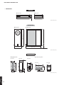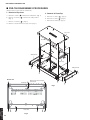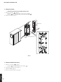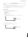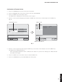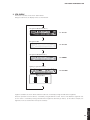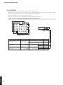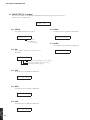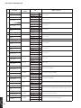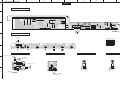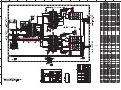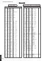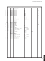
1
DVD HOME THEATER SYSTEM DVX-700
DVD CONTROLLER DVR-700
SUBWOOFER / SYSTEM CONTROL NS-PSW700
SPEAKERS NS-P700
SERVICE MANUAL
* The DVX-700 consists of the DVR-700, NS-PSW700 and NS-P700.
When accepting a repair order from the user, it is recommended to receive DVR-700, NS-PSW700 and NS-P700
as a set for the repair work.
* When DVD MODULE P.C.B. of the DVR-700 is replaced, the serial number and new device key (ID number)
MUST be reported to YCJ (Yamaha Corporation Japan) by email.
Email: [email protected]
For more information, refer to “SERVICE PRECAUTIONS”.
本资料由OKXIA视听皮带资源库www.okxia.cn提供
IMPORTANT NOTICE
This manual has been provided for the use of authorized YAMAHA Retailers and their service personnel.
It has been assumed that basic service procedures inherent to the industry, and more specifically YAMAHA Products, are already known
and understood by the users, and have therefore not been restated.
WARNING:
Failure to follow appropriate service and safety procedures when servicing this product may result in personal injury,
destruction of expensive components, and failure of the product to perform as specified. For these reasons, we advise
all YAMAHA product owners that any service required should be performed by an authorized YAMAHA Retailer or
the appointed service representative.
IMPORTANT: The presentation or sale of this manual to any individual or firm does not constitute authorization, certification or
recognition of any applicable technical capabilities, or establish a principle-agent relationship of any form.
The data provided is believed to be accurate and applicable to the unit(s) indicated on the cover. The research, engineering, and service
departments of YAMAHA are continually striving to improve YAMAHA products. Modifications are, therefore, inevitable and
specifications are subject to change without notice or obligation to retrofit. Should any discrepancy appear to exist, please contact the
distributor's Service Division.
WARNING:
Static discharges can destroy expensive components. Discharge any static electricity your body may have
accumulated by grounding yourself to the ground buss in the unit (heavy gauge black wires connect to this buss).
IMPORTANT: Turn the unit OFF during disassembly and part replacement. Recheck all work before you apply power to the unit.
■ CONTENTS
TO SERVICE PERSONNEL ........................................2–3
PREVENTION OF ELECTROSTATIC DISCHARGE ......4
REGION MANAGEMENT INFORMATION .....................5
SYSTEM COMPOSITION ................................................5
FRONT PANELS .........................................................6–8
REAR PANELS ......................................................... 9–10
REMOTE CONTROL PANELS ..................................... 11
SPECIFICATIONS ................................................... 12–14
INTERNAL VIEW .......................................................... 15
SERVICE PRECAUTIONS ...................................... 16–17
DVR-700 DISASSEMBLY PROCEDURES ............. 18–20
NS-PSW700 DISASSEMBLY PROCEDURES .......21–23
Copyright © 2008
All rights reserved.
This manual is copyrighted by YAMAHA and may not be copied or
redistributed either in print or electronically without permission.
P.O.Box 1, Hamamatsu, Japan
animate '08.12
DVR-700/
NS-PSW700/NS-P700
1011 2 0
UPDATING FIRMWARE ..........................................24–37
SELF-DIAGNOSTIC FUNCTION ............................38–63
DISPLAY DATA .......................................................64–65
IC DATA ...................................................................66–83
PIN CONNECTION DIAGRAMS .............................84–86
BLOCK DIAGRAMS ................................................87–89
PRINTED CIRCUIT BOARDS .................................90–98
SCHEMATIC DIAGRAMS ..................................... 99–106
REPLACEMENT PARTS LIST .............................107–117
REMOTE CONTROL ............................................118–119
SYSTEM MENU ........................................................... 120
DVR-700/NS-PSW700/NS-P700
■ TO SERVICE PERSONNEL
1. Critical Components Information
Components having special characteristics are marked
and
must be replaced with parts having specifications equal to those
originally installed.
WALL
OUTLET
2. Leakage Current Measurement (For 120V Models Only)
When service has been completed, it is imperative to verify
that all exposed conductive surfaces are properly insulated
from supply circuits.
• Meter impedance should be equivalent to 1500 ohms shunted
by 0.15 μF.
EQUIPMENT
UNDER TEST
AC LEAKAGE
TESTER OR
EQUIVALENT
INSULATING
TABLE
• Leakage current must not exceed 0.5mA.
• Be sure to test for leakage with the AC plug in both polarities.
For U model
“CAUTION”
“F701: FOR CONTINUED PROTECTION AGAINST RISK OF FIRE, REPLACE ONLY WITH SAME TYPE 5A, 125V
FUSE.”
For C model
CAUTION
F701: REPLACE WITH SAME TYPE 5A, 125V FUSE.
ATTENTION
F701: UTILISER UN FUSIBLE DE RECHANGE DE MÉME TYPE DE 5A, 125V.
WARNING: CHEMICAL CONTENT NOTICE!
This product contains chemicals known to the State of California to cause cancer, or birth defects or other reproductive
harm.
DO NOT PLACE SOLDER, ELECTRICAL/ELECTRONIC OR PLASTIC COMPONENTS IN YOUR MOUTH FOR ANY REASON
WHATSOEVER!
Avoid prolonged, unprotected contact between solder and your skin! When soldering, do not inhale solder fumes or
expose eyes to solder/flux vapor!
If you come in contact with solder or components located inside the enclosure of this product, wash your hands before
handling food.
About lead free solder
All of the P.C.B.s installed in this unit and solder joints are soldered using the lead free solder.
Among some types of lead free solder currently available, it is recommended to use one of the following types for the
repair work.
• Sn + Ag + Cu (tin + silver + copper)
• Sn + Cu (tin + copper)
• Sn + Zn + Bi (tin + zinc + bismuth)
Caution:
As the melting point temperature of the lead free solder is about 30°C to 40°C (50°F to 70°F) higher than that of the lead
solder, be sure to use a soldering iron suitable to each solder.
WARNING: Laser Safety
This product contains a laser beam component. This component may emit invisible, as well as visible radiation,
which may cause eye damage. To protect your eyes and skin from laser radiation, the following precautions must
be used during servicing of the unit.
DVR-700/
NS-PSW700/NS-P700
1) When testing and/or repairing any component within the product, keep your eyes and skin more than 30 cm/1 feet
away from the laser pick-up unit at all times. Do not stare at the laser beam at any time.
2) Do not attempt to readjust, disassemble or repair the laser pick-up, unless noted elsewhere in this manual.
3) CAUTION: Use of controls, adjustments or performance of procedures other than those specified herein may result in
hazardous radiation exposure.
2
DVR-700/NS-PSW700/NS-P700
Laser Emitting conditions:
1) When the Top Cover is removed, and the STANDBY/ON SW is turned to the “ON” position, the laser component will
emit a beam for several seconds to detect if a disc is present. During this time (5-10 sec.) the laser may radiate
through the lens of the laser pick-up unit. Do not attempt any servicing during this period!
If no disc is detected, the laser will stop emitting the beam. When a disc is loaded, you will not be exposed to any
laser emissions.
2) The laser power level can be adjusted with the VR on the pick-up PWB, however, this level has been set by the factory
prior to shipping from the factory. Do not adjust this laser level control unless instruction is provided elsewhere in this
manual. Adjustment of this control can increase the laser emission level from the device.
Laser Diode Properties
Type:
Semiconductor laser ALGaInP
Output Power:
Wave length:
655 nm (DVD) / 790 nm (VCD/CD)
Beam divergence: 20 degrees
U, C models
5 mW (DVD) / 7 mW (VCD/CD)
A, G, F, L, V models
Warning for power supply
The primary side of the power supply carries live mains voltage when the player is connected to the mains even
when the player is switched off !
This primary area is not shielded so it is possible to accidentally touch copper tracks and/or components when servicing
the player.
Service personnel have to take precautions to prevent touching this area or components in this area.
Note:
The screws on the DVD mechanism may never be touched, removed or re-adjusted.
Handle the DVD mechanism with care when the unit has to be exchanged!
The DVD mechanism is very sensitive for dropping or giving shocks.
DVR-700/
NS-PSW700/NS-P700
3
DVR-700/NS-PSW700/NS-P700
■ PREVENTION OF ELECTROSTATIC DISCHARGE
Some semiconductor (solid state) devices can be damaged easily by static electricity. Such components commonly are
called Electrostatically Sensitive (ES) Devices. Examples of typical ES devices are integrated circuits and some field-effect
transistors and semiconductor “chip” components. The following techniques should be used to help reduce the incidence
of component damage caused by electro static discharge (ESD).
1. Immediately before handling any semiconductor component or semiconductor-equipped assembly, drain off any ESD
on your body by touching a known earth ground. Alternatively, obtain and wear a commercially available discharging
ESD wrist strap, which should be removed for potential shock reasons prior to applying power to the unit under test.
2. After removing an electrical assembly equipped with ES devices, place the assembly on a conductive surface such as
aluminum foil, to prevent electrostatic charge buildup or exposure of the assembly.
3. Use only a grounded-tip soldering iron to solder or unsolder ES devices.
4. Use only an anti-static solder removal device. Some solder removal devices not classified as “anti-static (ESD protected)” can generate electrical charge sufficient to damage ES devices.
5. Do not use freon-propelled chemicals. These can generate electrical charges sufficient to damage ES devices.
6. Do not remove a replacement ES device from its protective package until immediately before you are ready to install it.
(Most replacement ES devices are packaged with leads electrically shorted together by conductive foam, aluminum foil
or comparable conductive material).
7. Immediately before removing the protective material from the leads of a replacement ES device, touch the protective
material to the chassis or circuit assembly into which the device will be installed.
CAUTION: Be sure no power is applied to the chassis or circuit, and observe all other safety precautions.
8. Minimize bodily motions when handling unpackaged replacement ES devices. (Otherwise harmless motion such as
brushing together of your fabric clothes or lifting of your foot from a carpeted floor can generate static electricity (ESD)
sufficient to damage an ES device).
Grounding for electrostatic breakdown prevention
1. Human body grounding.
Use the antistatic wrist strap to discharge the static electricity from your body.
2. Work table grounding.
Put a conductive material (sheet) or steel sheet on the area where the optical pickup is placed and ground the sheet.
Caution:
The static electricity of your clothes will not be grounded through the wrist strap. So take care not to let your clothes touch
the optical pickup.
Anti-static wrist strap
1M-ohms
DVR-700/
NS-PSW700/NS-P700
Conductive material
(sheet) or steel sheet
4
DVR-700/NS-PSW700/NS-P700
■ REGION MANAGEMENT INFORMATION
Region Management Information: This DVD player is designed and manufactured to respond to the Region
Management Information that is recorded on a DVD disc. If the Region number described on the DVD disc does
not correspond to the Region number of this DVD player, this DVD player cannot play this disc.
This product incorporates copyright
protection technology that is protected
by method claims of certain U.S. patents
and other intellectual property rights
o w n e d b y M a c ro v i s i o n C o r p o r a t i o n
and other rights owners. Use of this
copyright protection technology must be
authorized by Macrovision Corporation,
and is intended for home and other
limited viewing uses only unless
otherwise authorized by Macrovision
Corporation. Reverse engineering or
disassembly is prohibited.
5
2
1
6
2
2
3
5
4
4
2
■ SYSTEM COMPOSITION
The DVX-700 consists of the DVR-700, NS-PSW700 and NS-P700.
DVX-700
▼ NS-PSW700
▼ NS-P700 L / R
▼ DVR-700
DVR-700/
NS-PSW700/NS-P700
5
DVR-700/NS-PSW700/NS-P700
■ FRONT PANELS
DVR-700
U, C, A, G, F, L, V models
(U, C model)
(A, G, F, L, V models)
▼ Top view
DVR-700/
NS-PSW700/NS-P700
▼ Front view
6
POWER indicators
DVR-700/NS-PSW700/NS-P700
NS-PSW700
U, C, A, G, F, L, V models
▼ Top view
▼ Front view
▼ Side view
DVR-700/
NS-PSW700/NS-P700
7
DVR-700/NS-PSW700/NS-P700
DVR-700/
NS-PSW700/NS-P700
NS-P700
8
NS-P700 L
▼ Top view
▼ Side view
▼ Front view
▼ Side view
NS-P700 R
▼ Top view
▼ Side view
▼ Front view
▼ Side view
DVR-700/NS-PSW700/NS-P700
■ REAR PANELS
DVR-700
U, C, A, G, F, L, V models
U, C models
A model
G model
F model
L, V models
DVR-700/
NS-PSW700/NS-P700
9
DVR-700/NS-PSW700/NS-P700
NS-PSW700
U, C, A, G, F, L, V models
A model
L model
G, F models
V model
U, C models
U, C models
U, C models
NS-P700
U, C, A, G, F, L, V models
DVR-700/
NS-PSW700/NS-P700
NS-P700 L
10
NS-P700 R
DVR-700/NS-PSW700/NS-P700
■ REMOTE CONTROL PANELS
U, C models
A, L, V models
G, F models
DVR-700/
NS-PSW700/NS-P700
11
DVR-700/NS-PSW700/NS-P700
■ SPECIFICATIONS
DVR-700
NS-P700
■ Input/Output Section
■ Speaker Section
Input Terminal
Others .............................................................................USB
Type ..................................................Magnetic shielding type
Output Terminal
Video .......................................................VIDEO (composite)
COMPONENT (Y, PB, PR)
HDMI
Others ...............................................SYSTEM CONNECTOR
■ General
Dimensions (W x H x D)
.............................................360 mm x 68 mm x 224 mm
(14-3/16" x 2-11/16" x 8-13/16")
Weight ..................................................2.6 kg (5 lbs. 11 oz.)
Finish
Black color ................................. U, C, A, G, F, L, V models
NS-PSW700
■ Speaker Section
Type ............................................ Bass reflex speaker system
Magnetic shielding type
Driver
Woofer .................................. 16 cm (6-5/16") cone type x 1
Frequency Response
.................................................... 35 Hz to 130 kHz (-10dB)
Driver
Woofer ................................. 5.5 cm (2-3/16") cone type x 2
Tweeter ......................2.5 cm (1") balanced dome type x 1
Frequency Response
.................................................... 130 Hz to 20 kHz (-10dB)
Input Power
Nominal ......................................................................... 40 W
Maximum .................................................................... 100 W
■ General
Dimensions (W x H x D)
Excluding stands
...............................................95 mm x 190 mm x 98 mm
(3-3/4" x 7-1/2" x 3-7/8")
Including stands
Upright position
...........................................95 mm x 206 mm x 106 mm
(3-3/4" x 8-1/8" x 4-3/16")
Horizontal position
.........................................190 mm x 111 mm x 106 mm
(7-1/2" x 4-3/8" x 4-3/16")
Weight (Excluding stands)
.............................................................1.2 kg (2 lbs. 10 oz.)
Finish
Black color ................................. U, C, A, G, F, L, V models
■ Input/Output Section
Input Terminal
Analog audio ........................... INPUT4 (AUX L/R: pin jack)
Digital audio .......................................INPUT1, 2 (OPTICAL)
INPUT3 (COAXIAL)
Others ............................. DOCK (YDS-10, YDS-11, YBA-10)
FM antenna terminal
XM tuner (U, C models)
SIRIUS tuner (U, C models)
Output Terminal
Analog audio ................................................ SPEAKERS L/R
Others ...............................................SYSTEM CONNECTOR
■ General
Power Supply
U, C models ..................................................... AC 120 V, 60 Hz
A model ............................................................ AC 240 V, 50 Hz
G, F, L models .................................................. AC 230 V, 50 Hz
V model ............................................................ AC 110 V, 60 Hz
DVR-700/
NS-PSW700/NS-P700
Power Consumption
...................................................................................... 50 W
Maximum Power (JEITA, 6 ohms, 10 % THD)
SP OUT (1 kHz) ........................................................... 70 W
SUBWOOFER (100 Hz) ................................................ 70 W
Minimum RMS Output Power (6 ohms, 1 % THD)
SP OUT (1 kHz) ........................................................... 55 W
SUBWOOFER (100 Hz) ................................................ 55 W
Input Sensitivity/Input Impedance
AUX ......................................................... 350 mV/32 k-ohms
Maximum Input Signal Level (1 kHz, DSP=Thru)
AUX ................................................................. 2.2 V or more
Frequency Response (Analog, Digital input)
SP OUT .................................................. -2.0 ±1 dB (20 Hz)
0 dB (1 kHz)
-0.5 ±1 dB (20 kHz)
Standby Power Consumption (reference data)
.......................................................................Less than 1 W
Signal to Noise Ratio (IHF-A network)
SP OUT
Analog .........................................................82 dB or more
Digital ..........................................................98 dB or more
Dimensions (W x H x D)
Excluding legs ......................194 mm x 450 mm x 400 mm
(7-5/8" x 17-11/16" x 15-3/4")
Total Harmonic Distortion
(Analog, Digital 20 kHz-LPF, 1 kHz, 18.5 V/6 ohms)
SP OUT ..........................................................0.06 % or less
Weight .................................................13 kg (28 lbs. 10 oz.)
Residual Noise
(Analog, Digital 20 kHz-LPF, 1 kHz, 18.5 V/6 ohms)
SP OUT ...................................................................... 138 μV
Finish
Black color ................................. U, C, A, G, F, L, V models
12
■ Amplifier Section
DVR-700/NS-PSW700/NS-P700
■ DVD Section
Video Output
Composite .................................................1 Vp-p (75 ohms)
Y Output/Component Video Output
Component ...............................................1 Vp-p (75 ohms)
Manufactured under license from Dolby Laboratories. “Dolby”, “Pro
Logic”, “MLP Lossless” and the double-D symbol are trademarks of Dolby
Laboratories.
Pb Output/Component Video Output
Component ............................................0.7 Vp-p (75 ohms)
Pr Output/Component Video Output
Component ............................................0.7 Vp-p (75 ohms)
“DTS” and “DTS Digital Surround” are registered trademarks of DTS, Inc.
■ Tuner Section
FM Tuning Range
U, C models ....................................... 87.50 to 107.90 MHz
A, G, F, L, V models .......................... 87.50 to 108.00 MHz
DivX®, DivX® Ultra Certified, and associated logos
are trademarks of DivX®, Inc. and are used under
license.
* G, F models: RDS function 75 ohms unbalanced
■ Other Section
Sound Field (MOVIE, MUSIC, SPORTS, GAME)
......................................................................Surround mode
Night listening mode
Extended stereo
Compressed music enhancer
HDMI, the HDMI logo and High Definition Multimedia Interface are
trademarks or registered trademarks of HDMI Licensing LLC.
Virtual Surround Processor
.....................................................AIR SURROUND XTREME
Audio Decode
..........................................................................Dolby Digital
Dolby Pro Logic II
DTS
MPEG2
Speakers Distance Mode
........................................................ Wide / Normal / Narrow
■ General
Accessories
Remote control ................................................................ x 1
Battery (R6, AA, UM-3) ................................................... x 2
Indoor FM antenna (1.4 m) ............................................. x 1
Speaker cable ass’y (4 m) .............................................. x 2
System cable (4 m) ......................................................... x 1
Video pin cable (1.5 m) .................................................. x 1
Cover (for NS-PSW700) ................................................... x 1
Screw (for cover / 3x6) ................................................. x 6
Stand (for NS-P700) ........................................................ x 2
Nonskid pad (for stand) ............................................. x 18
Screw (for stand / 4x10) ............................................... x 2
*
U
C
A
G
The XM name and related logos are registered trademarks of XM Satellite
Radio Inc.
©2006 SIRIUS Satellite Radio Inc. “SIRIUS”, “SiriusConnect”, the SIRIUS
dog logo, channel names and logos are trademarks of SIRIUS Satellite
Radio Inc.
“Apple”, “iPod”, and “iTunes” are trademarks of Apple Inc., registered
in the U.S. and other countries.
Bluetooth is a registered trademark of Bluetooth SIG and is used by
Yamaha in accordance with a license agreement.
Windows Media is either a registered trademark or trademark of
Microsoft Corporation in the United States and/or other countries.
This product incorporates copyright protection technology that is
protected by U.S. patents and other intellectual property rights.
Use of this copyright protection technology must be authorized by
Macrovision, and is intended for home and other limited viewing uses
only unless otherwise authorized by Macrovision. Reverse engineering
or disassembly is prohibited.
Specifications are subject to change without notice due to product
improvements.
.......................U.S.A. model
.................Canadian model
................Australian model
.................European model
F .................... Russian model
L .................Singapore model
V ..................... Taiwan model
This system employs new technologies and algorithms that make it
possible to achieve 7-channel surround sound with only two speakers,
and without using wall reflections.
DVR-700/
NS-PSW700/NS-P700
13
DVR-700/NS-PSW700/NS-P700
• DIMENSIONS
DVR-700
▼ Side view
68
(2-11/16")
▼ Front view
360 (14-3/16")
224 (8-13/16")
Unit: mm (inch)
NS-PSW700
▼ Side view
450 (17-11/16")
▼ Front view
194 (7-5/8")
71.5
(2-13/16")
400 (15-3/4")
Unit: mm (inch)
NS-P700
▼ Upright position
▼ Horizontal position
95
(3-3/4")
98
(3-7/8")
Rear view
106
(4-3/16")
Front view
DVR-700/
NS-PSW700/NS-P700
14
126
(4-15/16")
96.5
(3-13/16")
50 (2")
78
(3-1/16")
Front view
190
(7-1/2")
106
(4-3/16")
111
(4-3/8")
Side view
206 (8-1/8")
Front view
Unit: mm (inch)
DVR-700/NS-PSW700/NS-P700
■ INTERNAL VIEW
DVR-700
Front view
1
2
3
4
1
2
3
4
5
6
7
8
8
7
9
6
5
9
10
10
OPERATION (4) P.C.B.
DVD MECHANISM UNIT
OPERATION (3) P.C.B.
OPERATION (2) P.C.B.
FRONT (2) P.C.B.
OPERATION (1) P.C.B.
OPERATION (6) P.C.B.
OPERATION (5) P.C.B.
FRONT (1) P.C.B.
DVD MODULE P.C.B.
Rear view
NS-PSW700
Side view
Rear view
11
11
12
13
14
DRIVER WOOFER
MAIN P.C.B.
SUB P.C.B.
POWER P.C.B.
13
12
14
DVR-700/
NS-PSW700/NS-P700
15
DVR-700/NS-PSW700/NS-P700
■ SERVICE PRECAUTIONS
When DVD MODULE P.C.B. of the DVR-700 is replaced, the serial number and new ID number (device key) must be reported to YCJ (Yamaha Corporation Japan) by email. (Fig. 1)
Email: [email protected]
[email protected]
[email protected]
DVR-700
Model name
Serial number of DVR-700
ID number (device key)
T015018XZ
008000215
Send this email to YCJ
Fig. 1
● Check the Serial Number
The serial number “SER.No.xxxxxxx” can be found at the rear panel of the DVR-700. (Fig. 2)
DVR-700 Rear view
Serial number
DVR-700/
NS-PSW700/NS-P700
Fig. 2
16
DVR-700/NS-PSW700/NS-P700
● Check the New ID Number (Device key)
Connection
Connect the VIDEO OUT terminal of DVR-700 to the VIDEO IN terminal of the TV monitor with a video pin cable.
Operation Procedure
Perform following steps while watching the TV monitor screen and using the keys on the remote
control.
3
1. With this unit in the standby mode, press the keys on the remote control in the order as shown
below.
The self-diagnostic function is activated. (Fig. 3)
2
1
Fig. 3
2. Press “
3. Press “
(down) ” key once to select main menu 22 DVD SETTING.
(right) ” key twice to select sub-menu 22-3 DVD ID CLR.
Self-diagnostic function starting display
1-1 VOL 1
Main menu 22 – DVD SETTING
DVD: -setting-
sub-menu 22-3 – DVD ID CLR
xxx:DVD ID CLR
Fig. 4
4. Press “ENTER” key once. Wait about 15 seconds.
5. New ID number (device key) will appear on TV monitor screen as shown below.
Note: While the ID number is displayed, never operate any keys on the remote control.
(Player's ID Number Setting)
ID Number ?
New ID number (device key)
* The displayed “008000215” is an
example.
0 0 8 0 0 0 2 1 5
Compare
* * * * * * * * *
<CLEAR>
Exit
Input ID Number !
Fig. 5
6. To exit the self-diagnostic function, press “STANDBY/ON” key to turn off the power.
DVR-700/
NS-PSW700/NS-P700
17
DVR-700/NS-PSW700/NS-P700
■ DVR-700 DISASSEMBLY PROCEDURES
(Remove parts in the order as numbered.)
1. Removal of Top Cover
a. Remove 3 screws (
b. Remove 3 screws (
(Fig. 1)
c. Remove 7 screws (
2. Removal of Frame Top
). Remove the side panel L. (Fig. 1)
a. Remove 7 screws (
). Remove the side panel R.
). (Fig. 1)
b. Remove 2 screws (
). (Fig. 2)
c. Remove the frame top. (Fig. 1)
). (Fig. 2)
d. Release a hook. Remove the top cover. (Fig. 1)
Top cover
Hook
4
4
4
1
Side panel L
4
3
3
Frame top
1
Side panel R
2
3
5
Bottom view
3
Front side 3
Remove the screw located
at the back.
3
3
2
DVR-700/
NS-PSW700/NS-P700
Fig. 1
Rear side
3
5
3
3
Fig. 2
18
5
3
DVR-700/NS-PSW700/NS-P700
3. Removal of FRONT (1) P.C.B.
4. Removal of Front Panel Ass’y
a. Remove 4 screws (
a. Remove 3 screws (
b. Remove screw (
). (Fig. 3)
) and 2 jack screws (
) and screw (
). (Fig. 3)
b. Release a hook. Remove the front panel ass’y. (Fig. 3)
). (Fig. 4)
c. Turn over the FRONT (1) P.C.B.. (Fig. 3)
d. Remove CB301, CB304-305, CB311, CB313-315,
CB317, CB319 and CB320-321. (Fig. 3)
e. Remove the FRONT (1) P.C.B.. (Fig. 3)
FRONT (1) P.C.B.
CB305
CB317
CB321
CB319
CB311
CB314
CB315
6
6
CB301
CB304
CB313
CB320
FRONT (1) P.C.B.
Hook
Front panel ass'y
9
10
Fig. 3
Rear view
8
8
7
19
DVR-700/
NS-PSW700/NS-P700
Fig. 4
DVR-700/NS-PSW700/NS-P700
5. Removal of DVD Mechanism Unit and DVD module P.C.B.
a. Remove 6 screws (
) and 2 screws (
). (Fig. 5)
b. Remove the DVD mechanism unit , DVD module P.C.B. and frame PCB together. (Fig. 5)
c. Remove CB9 and CN965. (Fig. 5)
d. Remove CN966, and ground the terminal side of the flexible flat cable with a clip or the like. (Fig. 5)
e. Remove 4 screws (
f.
). (Fig. 5)
Remove the DVD mechanism unit. (Fig. 5)
g. Remove 4 screws (
) and screw (
). Fig. 5)
h. Remove CN964. (Fig. 5)
i.
Remove the DVD module P.C.B.. (Fig. 5)
13
13
DVD mechanism unit
CB9
OPERATION (3) P.C.B.
12
12
15
Frame P.C.B.
CN966
CN964
CN965
14
14
DVD module P.C.B.
17 mm
(0.67")
Terminal side
DVR-700/
NS-PSW700/NS-P700
Clip
11
Use a clip or the like to ground
the unit.
20
11
Fig. 5
DVR-700/NS-PSW700/NS-P700
■ NS-PSW700 DISASSEMBLY PROCEDURES
(Remove parts in the order as numbered.)
Disconnect the power cable from the AC outlet.
1. Removal of Side Grille Ass’y
*
The side grille ass’y is fixed to the NS-PSW700
cabinet ass’y with dowels at 7 locations. As a
flatblade screwdriver is used for removal, use special
care not to cause damage to the NS-PSW700
cabinet ass’y.
a. First, insert a flatblade screwdriver at 3 dowel positions
and push up the side grille ass’y. (Fig. 1)
b. Next, using the metalblade or the like, push the side
grille ass’y upward until it comes off. (Fig. 1)
Note:
• Removing the side grille ass’y with the flatblade
screwdriver only without using the metalblade or
the like may cause damage to the side grille ass’y.
• When installing the side grille ass’y, apply quickdrying bond or the like to dowels and then fit them
into dowel holes for secure installation.
(The side grille ass’y will come off easily if its
dowels are fitted into dowel holes without applying
quick-drying bond or the like.)
2. Removal of Driver Woofer
a. Remove 4 screws (
). (Fig. 2)
b. Pull out the driver woofer.
c. Disconnect the connector connected to the terminal
of the driver woofer. (Fig. 2)
d. Remove the driver woofer. (Fig. 2)
Cabinet ass'y
Dowels
Connectors
Side grille ass'y
Flatblade screwdriver
Metalblade
Fig. 1
Driver woofer
1
Fig. 2
DVR-700/
NS-PSW700/NS-P700
21
DVR-700/NS-PSW700/NS-P700
3. Removal of Cover
*
If the cover (accessory) is installed, remove it first.
a. Remove 6 screws (
*
Screws (
). (Fig. 3)
) are identified with arrow marks (COVER
).
b. Remove the cover. (Fig. 3)
3
Cover
2
3
3
3
3
3
3
3
3
Fig. 3
4. Removal of Rear Panel Ass’y
*
Screws (
). (Fig. 3)
) are identified with arrow marks (
DVR-700/
NS-PSW700/NS-P700
b. Pull out the rear panel ass’y. (Fig. 3)
c. Remove CB802. (Fig. 3)
d. Remove the rear panel ass’y. (Fig. 3)
22
3
Rear panel ass'y
CB802
a. Remove 12 screws (
3
).
3
3
DVR-700/NS-PSW700/NS-P700
5. Removal of Chassis Cover Ass’y
a. Remove 14 screws (
) and 6 screws (
b. Remove the chassis cover ass’y. (Fig. 4)
). (Fig. 4)
4
Chassis cover ass'y
4
4
4
4
4
4
4
4
4
4
5
4
4
4
4
Fig. 4
When checking the P.C.B.s:
•
•
•
Spread the rubber sheet and the cloth.
Then place the rear panel ass’y on the cloth and
check it. (Fig. 5)
Reconnect all cables (connectors) that have been
disconnected.
When connecting the flexible flat cable, be careful
with polarity.
DVR-700
NS-PSW700
Rubber sheet and cloth
Fig. 5
23
DVR-700/
NS-PSW700/NS-P700
Rear panel ass'y
DVR-700/NS-PSW700/NS-P700
■ UPDATING FIRMWARE
When replacing the following parts, be sure to write the latest firmware.
Replaced parts
MAIN P.C.B.
Main
Microprocessor
(NS-PSW700)
yes
IC500 (Main microprocessor) of MAIN P.C.B.
(NS-PSW700)
IC303 (DSP (TI) flash ROM) of MAIN P.C.B.
(NS-PSW700)
Write the latest firmware to
SubDSP
Microprocessor
yes
Module Board
yes
yes
FRONT P.C.B.
(DVR-700)
yes
IC303 (Sub-microprocessor) of FRONT P.C.B.
(DVR-700)
yes
DVD module P.C.B.
(DVR-700)
yes
● Required tools
•
Windows 98/2000/Me/XP, PC with a serial port (RS232C)
•
Firmware downloader program
DSP_FLASHER_v3.0.exe : for main microprocessor
DSP_FLASHER_v2.7.exe : for DSP (TI FLASH ROM)
FlashSta.exe
: for sub-microprocessor
•
Firmware
D700_xxxxx.mot : for main microprocessor
DVX700_data1_verx_xx.hex : for DSP (TI FLASH ROM)
D700S_xxxx.mot : for sub-microprocessor
S8CAxxxx.BIN
: for module board
•
RS232C cross cable “D-sub 9 pin female”
(Specifications)
Pin No.2 RxD
Pin No.3 TxD
Pin No.5 GND
Pin No.7 RTS
Pin No.8 CTS
•
Pin No.2 RxD
Pin No.3 TxD
Pin No.5 GND
Pin No.7 RTS
Pin No.8 CTS
RS232C conversion adaptor (Part No.: WR492800)
● Preparation
1. For writing to the main microprocessor, DSP and sub-microprocessor:
Download firmware upgrading program and firmware from the specified source to the same folder of the PC.
2. For writing to the module board:
Make the Firmware CD by writing the firmware of module board into the root folder of the CD-R.
Set the CD volume label to “PIONEER”.
● Precautions
•
While writing firmware, keep the other application software on the PC closed.
It is also recommended to keep the software on the task tray closed as well.
•
Do not turn off the power while writing firmware.
● Confirmation of firmware version and checksum
DVR-700/
NS-PSW700/NS-P700
Before and after writing firmware, check the firmware version and checksum by using the self-diagnostic function
menu.
1. Start up the self-diagnostic function and select “11. CPU INFORMATION” menu.
2. Have the firmware version and checksum displayed by using sub-menu.
For more information, refer to “SELF-DIAGNOSTIC FUNCTION”.
24
DVR-700/NS-PSW700/NS-P700
● Connection Diagrams
NS-PSW700 rear panel
Writing port
PC
Serial port (RS232C)
RS232C conversion adaptor
RS232C cross cable
Flexible flat cable (9P)
SW301
FLASH
UCOM
OTHER
SW301
FLASH
UCOM
For main microprocessor
OTHER
For DSP
Connection Diagram 1
Tighten the screws.
NS-PSW700
Tighten the screws.
System cable
DVR-700
Connection Diagram 2
DVR-700/
NS-PSW700/NS-P700
25
DVR-700/NS-PSW700/NS-P700
PC
DVR-700 rear panel
Writing port
Serial port (RS232C)
RS232C conversion adaptor
RS232C cross cable
Flexible flat cable (9P)
SW301
FLASH
UCOM
OTHER
DVR-700/
NS-PSW700/NS-P700
Connection Diagram 3
26
DVR-700/NS-PSW700/NS-P700
Writing to the Main Microprocessor
Connection
1.
Connect the writing port of NS-PSW700 to the serial port (RS232C) of the PC with RS232C cross cable, RS232C
conversion adaptor and flexible flat cable. (See connection diagram 1)
2.
Set the switch (SW301) of RS232C conversion adaptor to the “FLASH UCOM” side. (See connection diagram 1)
Operation procedures
1.
Start up “DSP_FLASHER_v3.0.exe”.
“DSP FLASHER_V3.0” is displayed. (Fig. 1)
2.
Select the firmware.
Click [...]. (Fig. 1)
Select “D700_xxxxx.mot”. (Fig. 1)
Check to make sure that the serial port is open.
If “COM x opened!” is not displayed, it is possible that 232C port of the
PC has a problem.
When the mot file is loaded
The checksum of the ROM code is displayed in the frame of “mot sum:”
(to be used for confirmation after writing)
Fig. 1
Connect the power cable of the NS-PSW700 to the AC outlet.
27
DVR-700/
NS-PSW700/NS-P700
3.
DVR-700/NS-PSW700/NS-P700
4.
Click [E.P.] to start writing. (Fig. 2)
5.
When writing is completed, “Program Finished!” is displayed. (Fig. 2)
Click [OK]. (Fig. 3)
6.
Click [EXIT] to end “DSP FLASHER_v3.0.exe”. (Fig. 2)
Fig. 2
DVR-700/
NS-PSW700/NS-P700
7.
28
Disconnect the power cable of the NS-PSW700 from the AC outlet.
DVR-700/NS-PSW700/NS-P700
Writing to DSP
Connection
1.
Connect the writing port of the NS-PSW700 to the serial port (RS232C) of the PC with RS232C cross cable, RS232C
conversion adaptor and flexible flat cable. (See connection diagram 1)
2.
Set the switch (SW301) of RS232C conversion adaptor to the “OTHER” side. (See connection diagram 1)
3.
Connect the DVR-700 and the NS-PSW700 with the system cable (D-sub 15pin cable) supplied with this unit. (See
connection diagram 2)
Operation procedures
1.
Start up “DSP_FLASHER Ver2.7.exe”.
“DSP FLASHER_V2.70” is displayed. (Fig. 1)
2.
Click [Vx61 DSP]. (Fig. 1)
Fig. 1
DVR-700/
NS-PSW700/NS-P700
29
DVR-700/NS-PSW700/NS-P700
3.
Select the firmware.
Click [...]. (Fig. 2)
Select “DVX700_data1_verx_xx.hex”. (Fig. 2)
Check to make sure that the serial port is open.
If “COM x opened!” is not displayed, it is possible that 232C port of the
PC has a problem.
When the hex file is loaded
The checksum of the ROM code is displayed in the frame of “SUM from
FILE” (to be used for confirmation after writing)
DVR-700/
NS-PSW700/NS-P700
Fig. 2
30
4.
Connect the power cable of the NS-PSW700 to the AC outlet.
5.
Make sure that the DVR-700 is in the standby mode.
6.
Start up the self-diagnostic function mode by pressing the “TEST” key, “ON SCREEN” key and “STANDBY/ON” key on
the remote control in order.
7.
Select the “15-1 DSP STBY” menu by pressing the “ ▲ (up) ” (Forward) key and “ ▼ (down) ” (Reverse) key on the
remote control.
DVR-700/NS-PSW700/NS-P700
8.
Click [RDY]. (Fig. 3)
Fig. 3
9.
Select the writing mode from "15-1 DSP STBY" by pressing the “ ▶ (right) ” (Forward) key.
Writing starts automatically. (Fig. 4)
Fig. 4
DVR-700/
NS-PSW700/NS-P700
31
DVR-700/NS-PSW700/NS-P700
10. When writing is completed, “Vx61 DSP Flash finished!” is displayed. (Fig. 5)
The power of this unit turns off/on automatically.
11. Click [EXIT] to end “DSP_FLASHER Ver2.7.exe”. (Fig. 5)
When writing is completed, “Vx61
DSP Flash finished!” is displayed.
Fig. 5
DVR-700/
NS-PSW700/NS-P700
12. Press the “STANDBY/ON” key of this unit to turn off the power.
32
DVR-700/NS-PSW700/NS-P700
Writing to Sub-Microprocessor
Connection
1.
Connect the writing port of the DVR-700 to the serial port (RS232C) of the PC with RS232C cross cable, RS232C
conversion adaptor and flexible flat cable. (See connection diagram 3)
2.
Set the switch (SW301) of RS232C conversion adaptor to the “FLASH UCOM” side. (See connection diagram 3)
3.
Connect the DVR-700 and NS-PSW700 with the system cable (D-sub 15pin cable) supplied with this unit.
(See connection diagram 2)
Operation procedures
1.
Connect the power cable of the NS-PSW700 to the AC outlet.
2.
Start up FlashSta.exe, then the screen will appear as shown below. (Fig. 1)
3.
Select the port and data to be transmitted. (Fig. 1)
4.
•
Select Program
Select Internal flash memory
•
RS232C
Select the port of RS-232C
*
For selection of the port, COM1 to 4 can be used.
As COM5 or higher port cannot be used, select out of COM 1 to 4 of the setting on the PC side.
Click [OK]. (Fig. 1)
Select Internal flash memory
Select the port of RS-232C
Fig. 1
5.
The screen will appear as shown below. (Fig. 2)
6.
Select “115200” for Baud rate (bps) and “40” for Program_intervals (ms). (Fig. 2)
7.
Click [OK]. (Fig. 2)
Baud rate (bps) = 115200
Program_intervals(ms) = 40
Fig. 2
DVR-700/
NS-PSW700/NS-P700
33
DVR-700/NS-PSW700/NS-P700
8.
“ID Check” is displayed. (Fig. 3)
Click [Refer...], and select “D700S_xxxx.mot”. (Fig. 3)
The ID code and MCU type are loaded when the file is selected. (Fig. 3)
9.
Click [OK]. (Fig. 3)
When [Refer...] is clicked, the
open file screen is displayed.
Select the firmware
“D700S_xxxx.mot”.
DVR-700/
NS-PSW700/NS-P700
Fig. 3
34
DVR-700/NS-PSW700/NS-P700
10. “M16C Flash Start” is displayed. (Fig. 4)
Click [E.P.R...], then “Erase OK?” is displayed. (Fig. 4)
Click [OK], then writing is started. (Fig. 4)
11. When writing is completed, “Program OK.” is displayed. (Fig. 4)
Click [OK]. (Fig. 4)
12. Click [EXIT] to end “FlashSta.exe”. (Fig. 4)
When click [E.P.R...], “Erase OK?” is displayed.
When click [OK], writing is started.
Writing
Collating
Click [OK].
Writing completed
Fig. 4
13. Disconnect the power cable of the NS-PSW700 from the AC outlet.
DVR-700/
NS-PSW700/NS-P700
35
DVR-700/NS-PSW700/NS-P700
Writing to the Module Board
Connection
1.
Connect the DVR-700 and NS-PSW700 with the system cable (D-sub 15pin cable) supplied with this unit.
(See connection diagram 3)
2.
Connect the VIDEO OUT terminal of the DVR-700 to the VIDEO IN terminal of the TV monitor with a video pin cable.
Operation procedures
1.
Connect the power cable of the NS-PSW700 to the AC outlet.
2.
Press the “STANDBY/ON” key of the DVR-700 to turn on the power.
3.
Insert the firmware CD to the disc slot.
4.
“Upgrade?” is displayed on the TV monitor screen. (Fig. 1)
5.
Press the “PLAY” key of the DVR-700, then writing of the firmware is started. (Fig. 1)
Upgrade File DETECTED
Upgrade ?
Press Play To Start
Fig. 1
6.
After a few minutes, the firmware CD is drained from a slot automatically.
Remove the firmware CD.
*
*
At this time, do not turn off the power as writing of the firmware is going on in this unit.
Writing takes about 1 minute.
7.
When writing is completed, the display on the TV monitor screen disappears.
8.
Press the “STANDBY/ON” key of this unit to turn off the power.
Writing being executed.
Upgrade File DETECTED
Upgrade File DETECTED
Upgrade ?
Press Play To Start
Upgrade ?
Press Play To Start
File Copying
UPGRADING
DVR-700/
NS-PSW700/NS-P700
Fig. 2
36
DVR-700/NS-PSW700/NS-P700
Confirmation of Firmware Version
1.
Press the “STANDBY/ON” key of this unit to turn on the power.
2.
Press the “DVD/USB” key on the remote control to select the input DVD/USB.
3.
Press the “SETUP” key on the remote control.
The SETUP menu is displayed on the TV monitor screen. (Fig. 3)
4.
Move the cursor to [Initial Settings] by pressing the “DOWN” key on the remote control and press the “ENTER” key.
(Fig. 3)
"Initial Settings" select
"Options" select
Initial Settings
Video Output
Language
Display
Options
Play Mode
Video Adjust
Initial Settings
Disc Navigator
Make advanced settings
Move
Select ENTER
Parental Lock
DivX(R) VOD
Off(us)
REGION : 2
ROM VERSION : 1.24
Exit
SETUP
Move
Select ENTER
Exit
SETUP
ROM version is displayed
Fig. 3
5.
Move the cursor to [Options] by pressing the “DOWN” key on the remote control and press the “ON SCREEN” key.
The ROM version is displayed. (Fig. 3)
*
When the displayed firmware version is different from written one, perform the “Writing to the Module Board”
procedure all over again.
6.
Press the “SETUP” key on the remote control to end the SETUP menu.
7.
Press the “STANDBY/ON” key of the DVR-700 to turn off the power.
DVR-700/
NS-PSW700/NS-P700
37
DVR-700/NS-PSW700/NS-P700
■ SELF-DIAGNOSTIC FUNCTION
This unit has self-diagnostic functions that are intended for inspection, measurement and location of faulty point.
There are 22 main menu items, each of which has sub-menu items.
Listed in the table below are menu items and submenu items.
Note that not all menu items listed will apply to the models covered in this service manual.
No.
Main menu
1 DSP THROUGH
2
MUTE CHECK
3
VFD CHECK
4
TEST TONE
5
DTS TEST TONE
6
SPEAKER SELECT
7
AD CHECK
8 DEVICE CHECK
9 RDS CHECK (G, F models)
10 SET DESTINATION
11 CPU INFORMATION
12 EMC TEST
13 AUTO SLEEP
DVR-700/
NS-PSW700/NS-P700
14 ERROR INFORMATION
15 UPDATE DSP
16 DOCK CHECK
38
1
2
3
4
1
2
1
2
3
4
1
2
3
1
2
3
4
5
6
1
2
1
2
3
4
5
6
7
8
9
1
1
1
2
1
2
3
4
5
6
7
8
9
1
1
2
1
2
3
4
5
1
1
Sub-menu
MASTER Vol. 1
MASTER Vol. 30
MASTER Vol. 60
MASTER Vol. 100
MASTER Vol. 60
AMP MUTE
ALL ON
ALL OFF
DIMMER
PATTERN
ALL OUTPUT
TURN CHANGEOVER
LFE OUTPUT
L:NML/R: NML
L: LF/R: RF
L: LS/R: RS
L: CTR/R: NONE
L: LF/R: LS
L: RF/ R: RS
SP LARGE
SP SMALL
DC_PRT/PRV_5SUB
PRV_30/PRV_CU
PRV_12/PRV_7i
PRV_5/PRV_5i
PRV_3.3/PRV_1.2
KEY0 / KEY1
DOCK
P1s / P2s
DVD / TE1 (Not applied to this model)
DEVICE CHECK
RDS CHECK
SELECT DEST
SET DEST
CPU VERSION
CPU SUM CHECK
TI VERSION
TI SUM CHECK
SUB Version
SUB SUM Version
XM Version
SIRIUS Version
DESTINATION
EMC TEST
ASLP ON
ASLP OFF
ERROR HISTORY 1
ERROR HISTORY 2
ERROR HISTORY 3
ERROR HISTORY 4
RESET HISTORY
DSP STANDBY
DOCK CHECK
(Not applied to this model)
(Not applied to this model)
(Not applied to this model)
(Not applied to this model)
(Not applied to this model)
(Not applied to this model)
(Not applied to this model)
(Not applied to this model)
DVR-700/NS-PSW700/NS-P700
No.
Main menu
17 SWFR CROSS OVER
18 FACTORY PRESET
19 SWEEP TEST
20 XM TEST
21 SIRIUS TEST
22 DVD SETTING
Sub-menu
1
2
3
4
5
6
7
8
9
1
2
1
1
2
3
4
5
6
7
8
9
10
11
1
2
3
4
5
6
7
1
2
3
4
CRSOVR 40Hz
CRSOVR 60Hz
CRSOVR 80Hz
CRSOVR 90Hz
CRSOVR 100Hz
CRSOVR 110Hz
CRSOVR 120Hz
CRSOVR 160Hz
CRSOVR 200Hz
INHIBIT
RESERVED
SWEEP TEST
1k - 1dB/44
1k -61dB/44
Mute /44
XM Tone/44
ISO Tone/44
1k - 1dB/32
1k -61dB/32
Mute /32
XM Tone/32
ISO Tone/32
Bus Power OFF
SIRIUS CHECK
SIRIUS Information
SIRIUS Version SSP
SIRIUS Version MAC
SIRIUS Version ADP
SIRIUS Version prd_id
SIRIUS Version seg_id
Setting
DVD ID WRITE
DVD ID CLEAR
Rewrite F/W
(Not applied to this model)
DVR-700/
NS-PSW700/NS-P700
39
DVR-700/NS-PSW700/NS-P700
● Connection
1. Connect the DVR-700 and NS-PSW700 with the system cable (D-sub 15pin cable) supplied with this unit as shown
in the figure below.
2. Connect the power cable of the NS-PSW700 to AC outlet.
NS-PSW700
Tighten the screws.
Tighten the screws.
System cable
DVR-700
DVR-700/
NS-PSW700/NS-P700
To AC outlet
40
DVR-700/NS-PSW700/NS-P700
● Starting Self-Diagnostic Function
With this unit in the standby mode, press the keys on the remote control in the order as shown below.
The self-diagnostic function mode is activated and an opening message (the protection history) appears for a few
seconds followed by the main menu display (1-1 VOL 1).
3
2
1
Opening message
After a few seconds
Main menu display
DVR-700/
NS-PSW700/NS-P700
41
DVR-700/NS-PSW700/NS-P700
● Starting Self-Diagnostic Function in the protection cancel mode
If the protection function works and causes hindrance to trouble diagnostic, cancel the protection function as
described below, and it will be possible to enter the self-diagnostic function mode. (The protection functions other than
the excess current detect function will be disabled.)
With this unit in the standby mode, press the keys on the remote control in the order as shown below.
The self-diagnostic function mode is activated and an opening message (the protection history) appears for a few
seconds followed by the main menu display (1-1 VOL 1).
In this mode, the [SLEEP] segment of the FL display of this unit flashes to indicate that the mode is self-diagnostic
function mode with the protection functions disabled.
3
2
1
Opening message
Flashes
After a few seconds
Flashes
DVR-700/
NS-PSW700/NS-P700
Main menu display
CAUTION!
Using this product with the protection function disabled
may cause further damage to this unit.
Use special care for this point when using this mode.
42
DVR-700/NS-PSW700/NS-P700
● Canceling Self-Diagnostic Function
1. Before canceling self-diagnostic function, execute setting for FACTORY PRESET of main menu No. 18 (Memory
initialization inhibited or Memory initialized).
*
In order to keep the user memory stored, be sure to select INIT INHI (Memory initialization inhibited).
2. Press the “STANDBY/ON” key of this unit to turn off the power.
● Operation procedure of Main menu and Sub-menu
There are 22 menu items, each having sub-menu items.
Main menu selection
Select the main menu using “ ▲ (up) ” (Forward) key and “ ▼ (down) ” (Reverse) key on the remote control.
Sub-menu selection
Select the sub-menu using “ ▶ (right) ” (Forward) key and “ ◀ (left) ” (Reverse) key on the remote control.
Forward
Forward
Main menu selection
Sub-menu selection
Reverse
Reverse
● Functions in Self-Diagnostic Function mode
In addition to the self-diagnostic function menu items, functions as listed below are available.
•
•
•
•
•
•
•
•
[DVD/USB]
[INPUT1]
[INPUT2]
[INPUT3]
[INPUT4]
[TUNER]
[DOCK]
[STANDBY/ON]
: Signal input DVD/USB is selected.
: Signal input OPTICAL1 is selected.
: Signal input OPTICAL2 is selected.
: Signal input COAXIAL is selected.
: Signal input ANALOG is selected.
: Signal input FM tuner is selected.
: Signal input DOCK is selected.
: The self-diagnostic function mode is canceled and the stand-by mode starts.
DVR-700/
NS-PSW700/NS-P700
43
DVR-700/NS-PSW700/NS-P700
● Details of Self-Diagnostic Function menu
1. DSP THROUGH
2. MUTE CHECK
The output level can be selected by using submenu.
The signal is output in digital full-bit without
including the head margin. (L/R: 0dBm, SW: 0dBm)
The multi-channel source, center and surround L/R
channels are not output.
The 2ch stereo source, L channel signal with L.P.F.
is assigned to sub-woofer channel.
Select the input using the INPUT key (INPUT4 for
default).
1-1
2-1
VOL 1
MASTER Vol. = 1 (-90dB, MIN. VOLUME)
MASTER Vol. = 60 (-20dB), MUTE OFF
1-1 VOL 1
1-2
VOL 30
MASTER Vol. = 30 (-40dB)
1-2 VOL 30
1-3
VOL 60
MASTER Vol. = 60 (-20dB)
1-3 VOL 60
1-4
VOL 100
MASTER Vol. = 100 (0dB, MAX. VOLUME)
DVR-700/
NS-PSW700/NS-P700
1-4 VOL 100
44
VOL 60
2-1 VOL 60
2-2
AMP MUTE
Digital Amp MUTE.
The MUTE terminal of PWM processor
“ TA S 5 0 8 6 ” i s c o n t r o l l e d t h r o u g h t h e
microprocessor.
2-2 AMP MUTE
DVR-700/NS-PSW700/NS-P700
3. VFD CHECK
This menu is used to check the FL and FL driver.
Using the sub-menu, the display varies as shown below.
All segments ON (dimmer 100 %)
3-1 ALL ON
All segments OFF
3-2 ALL OFF
All segments ON (dimmer 50 %)
3-3 DIMMER
Lighting of segments in lattice
3-4 PATTERN
Lighting in lattice
Short
Normal
Segment conditions of the FL driver and the FL tube are checked by turning ON and OFF all segments.
Next, the operation of the FL driver is checked by using the dimmer control. Then a short between segments next
to each other is checked by turning ON and OFF all segments alternately (in lattice). (In the above example, the
segments in the second row from the top are shorted.)
DVR-700/
NS-PSW700/NS-P700
45
DVR-700/NS-PSW700/NS-P700
4. TEST TONE
The built-in noise generator outputs the test tone through the channels specified by the sub-menu.
The noise frequency for LFE (SUBWOOFER) is 35 to 80 Hz. Other than that, the noise frequency is 500 to 2 kHz.
4-1
All OUT
A test tone is output from all the speakers.
4-1 ALL OUT
4-2
TURN CHANGEOVER
Every time the “MUSIC” key on the remote control is pressed, a test tone is output from each channel in the
following order.
4-2 TEST ALL
4-2 TEST FL
Test tone is output from all channels.
Te s t t o n e i s o u t p u t f ro m t h e F R O N T L
channel.
4-2 TEST LFE
4-2 TEST FR
Test tone is output from the SUBWOOFER
channel.
Te s t t o n e i s o u t p u t f ro m t h e F R O N T R
channel.
"MUSIC" key
4-3
LFE OUT
A test tone is output from the subwoofer.
DVR-700/
NS-PSW700/NS-P700
4-3 LFE OUT
46
DVR-700/NS-PSW700/NS-P700
5. DTS TEST
6. SPEAKER SELECT
Not applied to this model.
Not applied to this model.
5-1
6-1
L: N / R: N
5-1 L:N
5-2
R:N
L: LF / R: RF
5-3
6
6-2
5-2 L:LF R:RF
SP SMALL
SP SMALL
SP LARGE
6
SP LARGE
L: LS / R: RS
5-3 L:LS R:RS
5-4
L: C / R: --
5-4 L:C
5-5
R:--
L: LF / R: LS
5-5 L:LF R:LS
5-6
L: RF / R: RS
5-6 L:RF R:RS
DVR-700/
NS-PSW700/NS-P700
47
DVR-700/NS-PSW700/NS-P700
7. AD CHECK
This menu is used to display the A/D conversion value of the microprocessor which detects panel keys of this unit
and protection functions by using the sub-menu.
7-1
DC: / 5S:
DC:
DC voltage of speaker output
Normal value:
82 to 173
(Reference voltage: 5.0 V=255)
Detection for AD port: DC_PRT
(126 pin of main microprocessor IC500 of MAIN P.C.B.)
5S:
Power supply voltage +5SUB (for microprocessor)
Normal value:
179 to 255
(Reference voltage: 5.0 V=255)
Detection for AD port: PRV_5SUB
(120 pin of main microprocessor IC500 of MAIN P.C.B.)
DC:131 5S:255
7-2
30: / CU:
30:
Power supply voltage +30D (for digital amplifier)
Normal value:
103 to 178
(Reference voltage: 5.0 V=255)
Detection for AD port: PRV_30
(123 pin of main microprocessor IC500 of MAIN P.C.B.)
CU:
Power supply voltages +15D and -29VP (for DVR-700)
Normal value:
48 to 222
(Reference voltage: 5.0 V=255)
Detection for AD port: PRV_CU
(124 pin of main microprocessor IC500 of MAIN P.C.B.)
DVR-700/
NS-PSW700/NS-P700
30:142 CU:127
48
DVR-700/NS-PSW700/NS-P700
7-3
12: / 7i:
12:
Power supply voltages +12D, +12A and +10T (for digital amplifier/analog audio)
Normal value:
106 to 162
(Reference voltage: 5.0 V=255)
Detection for AD port: PRV_12
(125 pin of main microprocessor IC500 of MAIN P.C.B.)
7i:
Power supply voltage +7i (for DOCK)
Normal value:
64 to 181
(Reference voltage: 5.0 V=255)
Detection for AD port: PRV_7i
(112 pin of main microprocessor IC500 of MAIN P.C.B.)
12:135 7i:142
7-4
5: / 5i:
5:
Power supply voltages +5D and +5.3D (for digital circuit)
Normal value:
104 to 155
(Reference voltage: 5.0 V=255)
Detection for AD port: PRV_5
(134 pin of main microprocessor IC500 of MAIN P.C.B.)
5i:
Power supply voltage +5i (for DOCK)
Normal value:
97 to 158
(Reference voltage: 5.0 V=255)
Detection for AD port: PRV_5i
(135 pin of main microprocessor IC500 of MAIN P.C.B.)
5:125 5i:013
DVR-700/
NS-PSW700/NS-P700
49
DVR-700/NS-PSW700/NS-P700
7-5
3: / 1P2:
3:
Power supply voltage +3.3D (for digital circuit)
Normal value:
86 to 141
(Reference voltage: 5.0 V=255)
Detection for AD port: PRV_3.3
(136 pin of main microprocessor IC500 of MAIN P.C.B.)
1P2:
Power supply voltage +1.2D (for DSP IC)
Normal value:
42 to 81 (Reference voltage: 5.0 V=255)
Detection for AD port: PRV_1.2
(137 pin of main microprocessor IC500 of MAIN P.C.B.)
3:113 1P2:062
7-6
KY0: / KY1:
KY0 / KY1:
Panel key of this unit. (without “STANDBY/ON” key)
When the A/D conversion value of the panel key becomes out of the specified range, normal
operation will not be available.
In that case, check the constant of voltage dividing resistor, solder condition, etc. with referring to the
table below.
(Reference voltage: 5.0 V=255)
KY0:255KY1:255
Detection for AD port: KEY0 (39 pin of sub-microprocessor IC303 of OPERATION P.C.B.)
KEY1 (41 pin of sub-microprocessor IC303 of OPERATION P.C.B.)
DVR-700/
NS-PSW700/NS-P700
Key Input(A-D) Pull-Up Resistance 10 k-Ohms
50
Ohm
0
+ 680
+ 680
+ 15k
+ 13.5k
V
0 – 0.2
0.2 – 0.4
0.5 – 1.8
1.9 – 3.4
3.5 – 4.0
A/D value
0–8
10 – 20
24 – 94
95 – 175
176 – 206
KEY0 (39 pin)
—
EJECT
PLAY
VOLUME UP
VOLUME DOWN
Ohm
0
+ 1.2k
+ 1.2k
+ 12.7k
+ 5.3k
+ 2.7k
V
0 – 0.1
0.3 – 0.7
0.8 – 1.7
1.8 – 2.7
2.8 – 3.2
3.3 – 3.6
A/D value
0 – 14
15 – 38
39 – 89
90 – 141
142 – 166
167 – 184
KEY1 (41 pin)
—
—
STOP
INPUT
—
PAUSE
DVR-700/NS-PSW700/NS-P700
7-7
DOC:
DOCK:
DOCK type
(Reference voltage: 5.0 V=255)
DOC:255
DOCK detection for AD port (IC500 Microprocessor pin no. 133)
Pull-up resistance 10 k-ohms
DOCK type
Ohm
ID DOCK
(Pin no. 133)
7-8
DOCK
(Bluetooth)
0.56k
5-25
Reserved
Reserved
2.7k
5.6k
DOCK
(iPod)
10.0k
50-60
85-100
120-140
Reserved
(Development)
No connect
18.0k
39.0k
–
150-170
195-210
245-255
P1s: / P2s:
P1s:
Power supply voltage +5D (for digital circuit of DVR-700)
Normal value:
97 to 158
(Reference voltage: 5.0 V=255)
Detection for AD port: VPRT1
(43 pin of sub-microprocessor IC303 of OPERATION P.C.B.)
P2s:
Power supply voltages 6R3V, V+5V and 3R3V (for DVD module P.C.B.)
Normal value:
108 to 155 (INPUT select: DVD/USB), 0 (INPUT select: others)
(Reference voltage: 5.0 V=255)
Detection for AD port: VPRT2
(48 pin of sub-microprocessor IC303 of OPERATION P.C.B.)
P1s:132P2s:136
7-9
DVD: / TE1:
DVD: Voltage detect of DVD module (for DVR-700)
Normal value:
106 to 162 (INPUT select: DVD/USB), 0 (INPUT select: others)
(Reference voltage: 5.0 V=255)
Detection for AD port: VDET
(49 pin of sub-microprocessor IC303 of OPERATION P.C.B.)
TE1 (CU_THM):
Not applied to this model.
51
DVR-700/
NS-PSW700/NS-P700
DVD:169TE1:
DVR-700/NS-PSW700/NS-P700
8. DEVICE CHECK
The communication between devices and register access are checked automatically.
When an error is found, corresponding error message is displayed as shown below.
8 NO ERROR
No error detected.
8 ERR DIR
Error detection of DIR/CODEC (IC1).
8 ERR DSP
Error detection of DSP (IC303).
8 ERR SDRAM
Error detection of SDRAM (IC307).
8 ERR FLASH
Error detection of flash ROM (IC309).
8 ERR EEPROM
Error detection of EEPROM (IC501).
8 ERR DAMP
Error detection of PWM processor for digital amp (IC800).
MAIN P.C.B. of the NS-PSW700
DIR/CODEC
AK4588
(IC1)
SDRAM
16Mbit
(IC307)
EEPROM
BR24L04
(IC501)
DSP
DA70Y
(IC303)
MICROPROCESSOR
M32C
(IC500)
Flash ROM
4Mbit
(IC309)
PWM Processor
TAS5086
(IC800)
DVR-700/
NS-PSW700/NS-P700
9. RDS (G, F models)
This menu is used to check the RDS circuit.
When the RDS data is received, the program type appears on the FL display.
FM input is selected automatically in this menu.
87.5 MHz is set as default frequency.
9
52
RDS
DVR-700/NS-PSW700/NS-P700
10. SET DESTINATION
This menu is used to write the destination information in EEPROM.
Caution: After replacing MAIN P.C.B. or EEPROM (IC501 MAIN P.C.B.), be sure to change the destination
setting using this main menu. If the destination setting is not changed, “UNKNOWN DEST” is
displayed and proper operation is not available.
10-1 SELECT DESTINATION
Use the procedure described below to change the destination setting.
Every time the “MOVIE” key on the remote control is pressed, the destination setting item is displayed in
the order as shown below.
Have the desired destination setting displayed and select sub-menu “10-2 SET DESTINATION” by
pressing the “ ▶ (right) ” (Forward) key and “ ◀ (left) ” (Reverse) key on the remote control.
Caution: Selecting the destination setting item alone does not complete the procedure to change it.
Be sure to have Sub menu “10-2 SET DESTINATION” displayed.
No destination
U destination
10-1 DEST ?
C destination
10-1 DEST U
10-1 DEST C
"MOVIE" key
F destination
G destination
10-1 DEST F
10-1 DEST G
Forward
Sub-menu selection
Reverse
V destination
L destination
10-1 DEST V
A destination
10-1 DEST L
10-1 DEST A
10-2 SET DESTINATION
This sub-menu is used to write the destination setting, which is selected by using “10-1 SELECT DESTINATION”
menu, to the EEPROM (IC501 MAIN P.C.B.).
10-2 U
SET!
DVR-700/
NS-PSW700/NS-P700
53
DVR-700/NS-PSW700/NS-P700
11. CPU INFORMATION
The information on main microprocessor (CPU), DSP, sub-microprocessor (SUB-CPU), XM (U, C models), SIRIUS
(U, C models) and destination are displayed.
11-1
CPU version
11-7
The firmware version of the microprocessor is displayed.
The firmware version of XM is displayed.
11-1 C120D
11-2
XM VER. A002
CPU Checksum
11-8
The firmware checksum of the microprocessor is displayed.
SR VER. A002
DSP version
11-9
The firmware version of the DSP is displayed.
11-3 01.07u2
11-4
DSP Checksum
The firmware checksum of the DSP is displayed.
11-4 50F23480
11-5
SUB-CPU version
The firmware version of the sub-microprocessor is displayed.
11-5 SubC C057
11-6
SUB-CPU Checksum
DVR-700/
NS-PSW700/NS-P700
The firmware checksum of the sub-microprocessor is displayed.
11-6 Sum
54
SIRIUS version (U model)
The firmware version of SIRIUS is displayed.
11-2 CD11
11-3
XM version (U, C models)
FA8B
DEST
The destination information written in EEPROM is displayed.
11-9 DEST U
DEST ?
DEST U
DEST C
DEST G
DEST A
DEST L
DEST V
DEST F
= Unknown destination
= U model
= C model
= G model
= A model
= L model
= V model
= F model
DVR-700/NS-PSW700/NS-P700
12. EMC TEST
The signal is output in digital full-bit without including the head margin.
Select the input using the INPUT key (INPUT1 for default).
Output can be adjusted in the range of master volume control from -90 to 0 dB.
12
EMC VOL
13. AUTO SLEEP
ON/OFF of the auto-sleep function is setup.
These settings are retained until initialization by “18. FACTORY PRESET” is executed.
13-1 ASLP ON
An auto-sleep function is turned ON.
13
ASLP ON
13-2 ASLP OFF
An auto-sleep function is turned OFF.
13
ASLP OFF
DVR-700/
NS-PSW700/NS-P700
55
DVR-700/NS-PSW700/NS-P700
14. ERROR INFORMATION
The error information is displayed up to latest 4 errors.
When the same error is repeated, it is ignored.
This information is retained until sub-menu 14-5 is selected or EEPROM is initialized.
DVR-700/
NS-PSW700/NS-P700
14-1 to 14-4 ERROR INFORMATION
56
14-1 NoPRT
NO ERROR
14-1 TmpDaxxxx
Digital Amp TAS5342 (IC801, IC802 MAIN P.C.B.) over-temperature.
14-1 IPRTxxxxx
Digital Amp TAS5342 (IC801, IC802 MAIN P.C.B.) over-current.
14-1 DcPRTxxxx
Speaker output abnormal DC voltage.
14-1 PS_5Sxxxx
Abnormal voltage level. +5SUB (for main microprocessor)
14-1 PS_30xxxx
Abnormal voltage level. +30D (for digital amp)
14-1 PS_15xxxx
Abnormal voltage level. +15D, -29VP (for DVR-700)
14-1 PS_12xxxx
Abnormal voltage level. +12D, +12A, +10T (for digital amp and analog audio)
14-1 PS_7ixxxx
Abnormal voltage level. +7i (input of the power regulator for DOCK)
14-1 PS_5xxxxx
Abnormal voltage level. +5D, +5.3D (for digital circuit)
14-1 PS_5ixxxx
Abnormal voltage level. +5i (for DOCK)
14-1 PS_3xxxxx
Abnormal voltage level. +3.3D (for digital circuit)
14-1 PS_1P2xxx
Abnormal voltage level. +1.2D (for DSP)
14-1 SPS_1xxxx
Abnormal voltage level. +5D (for DVR-700 digital circuit)
14-1 SPS_2xxxx
Abnormal voltage level. 6R3V, V+5V, 3R3V (for DVD module P.C.B.)
DVR-700/NS-PSW700/NS-P700
14-1 SDVDxxxxx
Abnormal voltage level. VDET (for DVR-700 DVD module)
14-1 STE_1xxxx
Over-temperature of DVR-700.
(Not applied to this model.)
14-5 RST HIST !
When you select this menu and press the “ENTER” key on the remote control, then the error information
will be initialized.
14-5 RST HIST!
15. UPDATE DSP
This menu is used to write the DSP firmware. (See “Writing to DSP” of “UPDATING FIRMWARE”)
Note: Be sure to use this menu only for “writing to DSP”. Otherwise, all keys will become non-operable.
15-1 DSP STBY
After operating step 8 of “writng to DSP”, press the “ ▶ (right)” (forward) key on the remote control to start
writing.
When writing is started, the display is changed as shown below.
Standby mode
To press “ ▶ (right) ” (forward) key
Writing mode
“- -” is displayed.
If all keys have become non-operable, disconnect the power cable of this unit from the AC outlet.
DVR-700/
NS-PSW700/NS-P700
57
DVR-700/NS-PSW700/NS-P700
16. DOCK CHECK
This menu is used to check the DOCK connector without the iPod itself.
With the power to this unit turned off, short between pins No.14 (TX) and No. 18 (RX), between pins No. 1 (PWR)
and No. 17 (ACCPOW) and between pins No. 4 (iPDET) and No. 8 (DGND).
Start the self-diagnostic function and select this menu.
The check result is displayed according to the following display specifications.
Note)
Be sure to return the shorted locations to their original state.
15
16
17
18
9
10
11
12
13
14
3
4
5
6
7
8
19
20
21
2
16 DOCK:OK YYY
1
OK = all Y
NG = others
DOCK connector
Check item
UART loop back test
Short pins
Result
Display
Pins No.14 (TX)
– No.18 (RX)
OK
Y
NG
N
iPAP (iPod accessory power) Pins No.1 (PWR+)
IC500 (MAIN P.C.B.)
detection
– No.17 (ACCPWR)
pin No. 141 state
DVR-700/
NS-PSW700/NS-P700
iPDET (iPod installation to Pins No.4 (iPDET)
IC500 (MAIN P.C.B.)
DOCK) detection
– No.8 (DGND)
pin No. 4 state
58
High
Y
Low
N
Low
Y
High
N
⎫
⎪
⎬
⎪
⎭
⎫
⎪
⎬
⎪
⎭
⎫
⎪
⎬
⎪
⎭
DVR-700/NS-PSW700/NS-P700
17. SWFR CROSSOVER
This menu is used to set the crossover frequency of SUBWOOFER/Front L/R channels.
This setting is retained until EEPROM is initialized.
(Setting subwoofer level to 0 in advance.)
17-1 CRSOVR 40Hz
Cross Over Frequency = 40Hz
17 CRSOVR 40Hz
17-2 CRSOVR 60Hz
Cross Over Frequency = 60Hz
17 CRSOVR 60Hz
17-3 CRSOVR 80Hz
Cross Over Frequency = 80Hz
17 CRSOVR 80Hz
17-4 CRSOVR 90Hz
Cross Over Frequency = 90Hz
17 CRSOVR 90Hz
17-6 CRSOVR 110Hz
Cross Over Frequency = 110Hz
17 CRSOVR110Hz
17-7 CRSOVR 120Hz
Cross Over Frequency = 120Hz
17 CRSOVR120Hz
17-8 CRSOVR 160Hz
Cross Over Frequency = 160Hz
17 CRSOVR160Hz
17-9 CRSOVR 200Hz
Cross Over Frequency = 200Hz
17 CRSOVR200Hz
17-5 CRSOVR 100Hz
Cross Over Frequency = 100Hz
17 CRSOVR100Hz
DVR-700/
NS-PSW700/NS-P700
59
DVR-700/NS-PSW700/NS-P700
18. FACTORY PRESET
This menu is used to reserve and inhibit initialization of EEPROM.
18-1 INIT INHI (Initialization inhibited)
EEPROM initialization is not executed. Select this sub-menu to protect the user setting values.
18-1 INIT INHI
18-2 INIT RSRV (Initialization reserved)
Initialization of EEPROM is reserved. It is actually executed the next time when the power is turned on.
Select this sub-menu at factory shipment or before initialization of EEPROM. The destination information is
retained even after initialization.
18-2 INIT RSRV
CAUTION: Before setting to the INIT RSRV, write down the existing preset memory content of the tuner in a table
as shown below.
(This is because setting to the INIT RSRV will cause the user memory content of the tuner to be
erased.)
Preset Group
A
B
C
D
E
P1
P2
P3
P4
P5
P6
P7
P8
19. SWEEP TEST
For the sweep test of front and subwoofer speakers.
Front L/R and subwoofer output’s filter including cross-over frequency and DSP head margin should be same as
“stereo” mode in normal operation mode.
DVR-700/
NS-PSW700/NS-P700
19-1 SWEEP TEST
60
DVR-700/NS-PSW700/NS-P700
20. XM TEST (U, C models)
This menu is used to check the output of XM Satellite Radio.
Volume level is changed to 60.
VOLUME
20-1 1k -1dB/44
20-6 1k -1dB/32
The test tone (1kHz, -1dB/44.1kHz) is
output.
1k - 1dB/44
20-2 1k -61dB/44
1k - 61dB/44
20-3 Mute /44
1k - 1dB/32
The test tone (1kHz, -61dB/32kHz) is
output.
1k - 61dB/32
20-8 Mute /32
Nothing is output.
/44
20-4 XM Tone/44
The XM tone (44.1kHz) is output.
XM
The test tone (1kHz, -1dB/32kHz) is output.
20-7 1k -61dB/32
The test tone (1kHz, -61dB/44.1kHz) is
output.
Mute
60
Tone/44
20-5 ISO Tone/44
The ISO tone (44.1kHz) is output.
ISO Tone/44
Nothing is output.
Mute
/32
20-9 XM Tone/32
The XM tone (32kHz) is output.
XM
Tone/32
20-10 ISO Tone/32
The ISO tone (32kHz) is output.
ISO Tone/32
20-11 Bus Power OFF
The power of XM module is turned off.
61
DVR-700/
NS-PSW700/NS-P700
Bus Power:OFF
DVR-700/NS-PSW700/NS-P700
21. SIRIUS TEST (U, C models)
This menu is used to check SIRIUS Satellite Radio function by using Sirius Connect tuner.
Volume level is changed to 60.
VOLUME
21-1 SIRIUS:
60
21-6 PRDID:
The UART loop-back is checked.
The prd_id version of SIRIUS is displayed.
SIRIUS: --
PRDID:00 00 00
OK : Normal
NG : Abnormal
– – : Unconnected
21-7 SEGID:
The seg_id version of SIRIUS is displayed.
21-2 SR:
The SIRIUS antenna information is
displayed.
SR:FF 00 FF
Result of antenna diagnostic mode (status)
Antenna error history (SSP error codes)
Antenna generation (gen_id)
21-3 SSP:
The SSP version of SIRIUS is displayed.
SSP:
00 00 00
21-4 MAC:
The MAC version of SIRIUS is displayed.
MAC:
00 00 00
21-5 ADP:
DVR-700/
NS-PSW700/NS-P700
The ADP version of SIRIUS is displayed.
ADP:
62
00 00 00
SEGID:00 00 00
DVR-700/NS-PSW700/NS-P700
22. DVD SETTING
This mode is prepared mainly for manufacturing use.
Select “DVD ID CLR” to check the ID number (device key) of the module board.
See “Check the New ID number” for details.
22-1 DVD:
DVD: -setting-
22-2 ID WRITE
ID Write Ent01
22-3 ID CLEAR
xxx:DVD ID CLR
22-4 REWRITE F/W
xxx:ReWr
F/W
DVR-700/
NS-PSW700/NS-P700
63
DVR-700/NS-PSW700/NS-P700
■ DISPLAY DATA
V1: 17-BT-32GNK (OPERATION P.C.B.)
1
69
PATTERN AREA
PIN CONNECTION
Pin No.
69 68 67 66 65 64 63 62 61 60 59 58 57 56 55 54 53 52 51 50 49 48 47 46 45 44 43 42 41 40 39 38 37 36 35
Connection F2 NX NP NP P1 P2 P3 P4 P5 P6 P7 P8 P9 P10 P11 P12 P13 P14 P15 P16 P17 P18 P19 P20 P21 P22 P23 P24 P25 P26 P27 P28 P29 P30 P31
Pin No.
34 33 32 31 30 29 28 27 26 25 24 23 22 21 20 19 18 17 16 15 14 13 12 11 10 9 8 7 6 5 4 3 2 1
Connection P32 P33 P34 P35 P36 P37 NX NX NX NX NX NX NX 17G 16G 15G 14G 13G 12G 11G 10G 9G 8G 7G 6G 5G 4G 3G 2G 1G NP NP NX F1
Note : 1) F1, F2 ..... Filament pin
2) NP ..... No pin
3) NX ..... No extend pin
4) 1G~17G ..... Grid pin
GRID ASSIGNMENT
17G
16G
1G
2G
3G
4G
5G
6G
7G
S3
8G
9G
15G
10G 11G 12G 13G
S14
S1
S5
S6
S7
S8
S9
S10
14G
S11
S12
S13
S15
S4
(15G)
(16G)
1-1
2-1 3-1 4-1 5-1
1-2
2-2 3-2 4-2 5-2
1-3
2-3 3-3 4-3 5-3
S24
1-4
2-4 3-4 4-4 5-4
S25
S22
1-5
2-5 3-5 4-5 5-5
1-6
2-6 3-6 4-6 5-6
1-7
2-7 3-7 4-7 5-7
S26
(17G)
1a
S24
S23
S25
a
S21
S20
S19
f
S18
S2
2b
b
f
a
b
S29
S28
e
d
d
c
S28
S27
g
g
S29
c
e
DVR-700/
NS-PSW700/NS-P700
(96/24)
(1G-14G)
64
S16
S17
(DUAL)
S30
DVR-700/NS-PSW700/NS-P700
ANODE CONNECTION
17G
16G
1P
15G
S1
2P
14G
13G-1G
1-1
1-1
2-1
2-1
3P
S8
S15
3-1
3-1
4P
S9
S16
4-1
4-1
5P
S10
S2
5-1
5-1
6P
S3
S11
S18
1-2
1-2
7P
S5
S12
1a
2-2
2-2
8P
S6
S13
1b
3-2
3-2
9P
S7
S14
1c
4-2
4-2
10P
S4
1d
5-2
5-2
1e
1-3
1-3
1f
2-3
2-3
13P
1g
3-3
3-3
14P
2a
4-3
4-3
2b
5-3
5-3
2c
1-4
1-4
17P
2d
2-4
2-4
18P
2e
3-4
3-4
11P
12P
S21
15P
16P
(ES)
19P
S20
2f
4-4
4-4
20P
S19
2g
5-4
5-4
21P
S27
1-5
1-5
22P
S28
2-5
2-5
23P
S29
3-5
3-5
4-5
4-5
5-5
5-5
26P
1-6
1-6
27P
2-6
2-6
3-6
3-6
29P
4-6
4-6
30P
5-6
5-6
1-7
1-7
2-7
2-7
3-7
3-7
4-7
4-7
5-7
5-7
24P
25P
S17
28P
S30
31P
(HOLD)
32P
33P
S22
34P
S23
35P
S24
36P
S25
–
37P
S26
–
(RT)
DVR-700/
NS-PSW700/NS-P700
65
DVR-700/NS-PSW700/NS-P700
■ IC DATA
IC303: R5F21247SNFP (FRONT P.C.B.)
Sub-microprocessor
8
I/O ports
Port P0
8
8
Port P1
Port P2
6
3
Port P3
3
8
Port P4
Port P6
Peripheral functions
A/D converter
(10 bits x 12 channels)
System clock
generation circuit
Timers
Timer RA (8 bits)
Timer RB (8bits)
Timer RD
(16 bits x 2 channels)
Timer E (8 bits)
XIN-XOUT
High-speed on -chip oscillator
Low-speed on-chip oscillator
XCIN-XCOUT
UART or
clock synchronous serial I/O
(8 bits x 2 channels)
I2C bus interface or clock synchronous
serial I/O with chip select
(8 bits x 1 channel)
LIN module
(1 channel)
R8C/Tiny Series CPU core
Watchdog timer
(15 bits)
R0H
R1H
R0L
R1L
Memory
ROM(1)
SB
USP
R2
R3
ISP
RAM(2)
INTB
A0
A1
FB
PC
FLG
Multiplier
NOTES:
NC
KEY0
USB_OC
DAT_FL
CLK_FL
FREQ_FL
MCU_DAT
STBY/ON
SLT_SW 1
SLT_SW 2
PWR_DET
TxD_O
ACK
39
38
37
36
35
34
33
32
31
30
29
28
27
1. ROM size varies with MCU type.
2. RAM size varies with MCU type.
NC
40
26
NC
KEY1
41
25
THM_IN
ADIN
42
24
MCU_TX
VPRT 1
43
23
MUC_RX
VREF
44
22
MCU_CLK
21
REM_IN
IC303
66
Slt_FWD
45
Slt_REV
46
20
MCU_DAT
USB_EN
47
19
MTK_201_TRIN
VPRT2
48
18
MTK_200_TROUT
VDET
49
17
/RST_FL
Slot FWD
50
16
/CE_FL
Slot REV
51
15
PWR_FL
SDATA
52
14
PWR_LED
1
2
3
4
5
6
7
8
9
10
11
12
13
SCL
MDATA
XDVDRST
MODE
XREDADY
DVDPWR
/RESET
XIN
VSS
XOUT
VCC
PWR_DVD
R5F21247SNFP
NC
DVR-700/
NS-PSW700/NS-P700
YA347A0
DVR-700/NS-PSW700/NS-P700
Pin
No.
Function
Name
Port
Name
I/O
Detail of function
1
NC
2
SCL
P3_5
S-CLK
3
MDATA
P3_3
S-Rx
4
XDVDRST
P3_4
O
5
MODE
6
XREDADY
P4_3
O
XREADY
DVD
7
DVDPWR
P4_4
O
DVDPOWER
DVD
8
/RESET
9
XIN
SCLK
DVD
MDATA
DVD
XDVDRST
DVD
P4_7
20MHz
P4_6
20MHz
10 VSS
11 XOUT
12 VCC
13 PWR_DVD
P2_7
O
DVD_PS: DVD power supply control (H: ON/NonTuner, L: OFF/Tuner)
Front
14 PWR_LED
P2_6
O
PDLED: Power on LED (H: ON, L: OFF)
Front
15 PWR_FL
P2_5
O
PWR_FL: Power supply control of FL driver (H: ON, L: OFF)
Front
16 /CE_FL
P2_4
O
FL driver CE OUT
Front
17 /RST_FL
P2_3
O
FL driver RESET (turn off) OUT
Front
18 MTK_200_TROUT
P2_2
O
Tray open
DVD
19 MTK_201_TRIN
P2_1
O
20 MCU_DAT
P2_0
I (Timer)
21 REM_IN
P1_7
I (INT)
Cramp Fin
DVD
Transmission request interrupt from main to sub (Event capture
MainMCU
function)
Remote control input *2
Front
22 MCU_CLK
P1_6
I (S-CLK)
23 MUC_RX
P1_5
24 MCU_TX
P1_4
25 THM_IN
P1_3
I
Temperature detection
26 NC
NC
27 ACK
P4_5
I
ACK
28 TxD_O
P6_6
S-Tx
29 PWR_DET
P6_7
I
30 SLT_SW 2
P1_2
I (INT)
SlotIn detect 1
Loader
31 SLT_SW 1
P1_1
I (INT)
SlotIn detect 2
Loader
32 STBY/ON
P1_0
I (Timer)
Communication clock between MAIN and SUB
MainMCU
S-Rx
Communication data reception between MAIN and SUB
MainMCU
S-Tx
Communication data transmission between MAIN and SUB
MainMCU
Front
No used / PowerDownDetectIN
Terminal for interrupt of key input
33 MCU_DAT
P3_1
O
Ready signal from SUB to MAIN / Interrupt request
34 FREQ_FL
P3_0
O
No used / FL drive clock output (pulse output mode)
35 CLK_FL
P6_5
O (S-CLK)
36 DAT_FL
DVD
Front
MainCPU
Communication clock of the FL display
Front
O
Communication data of the FL display is transmitted
Front
Overcurrent detection
USB
Key0 input
Front
Key1 input
Front
37 USB_OC
P6_3
I
38 KEY0
P0_7
I (AD)
41 KEY1
P0_6
I (AD)
42 ADIN
P0_5
I
No used / Model distinction input
43 VPRT 1
P0_4
I (AD)
Power supply voltage detection 1
44 VREF
P4_2
45 Slt_FWD
P6_0
O
Loader FWD
Loader
46 Slt_REV
P6_2
O
Loader REV
Loader
47 USB_EN
P6_1
O
Enable
48 VPRT2
P0_3
I (AD)
49 VDET
P0_2
I (AD)
VDET
DVD
50 Slot FWD
P0_1
I
Tray FWD
DVD
Tray REV
DVD
SDATA
DVD
39 NC
40 NC
CU
Standard voltage IN
P0_0
I
P3_7
S-Tx
USB
CU
67
DVR-700/
NS-PSW700/NS-P700
51 Slot REV
52 SDATA
Power supply voltage detection 2
DVR-700/NS-PSW700/NS-P700
Detection for AD port: KEY0 (39 pin of sub-microprocessor IC303 of OPERATION P.C.B.)
KEY1 (41 pin of sub-microprocessor IC303 of OPERATION P.C.B.)
DVR-700/
NS-PSW700/NS-P700
Key Input(A-D) Pull-Up Resistance 10 k-Ohms
68
Ohm
0
+ 680
+ 680
+ 15k
+ 13.5k
V
0 – 0.2
0.2 – 0.4
0.5 – 1.8
1.9 – 3.4
3.5 – 4.0
A/D value
0–8
10 – 20
24 – 94
95 – 175
176 – 206
KEY0 (39 pin)
—
EJECT
PLAY
VOLUME UP
VOLUME DOWN
Ohm
0
+ 1.2k
+ 1.2k
+ 12.7k
+ 5.3k
+ 2.7k
V
0 – 0.1
0.3 – 0.7
0.8 – 1.7
1.8 – 2.7
2.8 – 3.2
3.3 – 3.6
A/D value
0 – 14
15 – 38
39 – 89
90 – 141
142 – 166
167 – 184
KEY1 (41 pin)
—
—
STOP
INPUT
—
PAUSE
DVR-700/NS-PSW700/NS-P700
M66003-0131FP (OPERATION P.C.B.)
FL display driver
Display code
RAM
(8-bit x 60)
CGROM
(35 bit x 166)
44
Segment
output
circuit
Code
write
CS 2
SCK 3
SDATA 4
Serial
receive
circuit
dot data
write
data
CGROM
(35 bit x 16)
Code/
command
control
circuit
19
SEG25
17
SEG26
9
SEG34
45
SEG35
52
51
code
select
XIN 7
XOUT
6
Clock
generator
timing
clock
Display
controller
Segment
digit
select/
output
circuit
scan pulse
50
49
48
47
46
Digit
output
circuit
RESET 1
8
DIG11/
SEG42
DIG12/
SEG41
DIG13/
SEG40
DIG14/
SEG39
DIG15/
SEG38
DIG16/
SEG37
DIG17/
SEG36
63
DIG00
53
DIG10
18
5
64
VP
DIG00
DIG01
DIG02
DIG03
DIG04
DIG05
DIG06
DIG07
DIG08
DIG09
DIG10
DIG11/SEG42
DIG12/SEG41
DIG13/SEG40
DIG14/SEG39
Vcc1
Vcc2
Vss
Vp
SEG00
64 63 62 61 60 59 58 57 56 55 54 53 52 51 50 49
RESET
CS
SCK
SDATA
Vss
XOUT
XIN
Vcc1
SEG34
SEG33
SEG32
SEG31
SEG30
SEG29
SEG28
SEG27
1
2
3
4
5
48
47
46
45
44
43
42
41
40
39
38
37
36
35
34
33
6
7
8
9
10
11
12
13
14
15
16
DIG15/SEG38
DIG16/SEG37
DIG17/SEG36
SEG35
SEG00
SEG01
SEG02
SEG03
SEG04
SEG05
SEG06
SEG07
SEG08
SEG09
SEG10
SEG11
17 18 19 20 21 22 23 24 25 26 27 28 29 30 31 32
69
DVR-700/
NS-PSW700/NS-P700
SEG26
Vcc2
SEG25
SEG24
SEG23
SEG22
SEG21
SEG20
SEG19
SEG18
SEG17
SEG16
SEG15
SEG14
SEG13
SEG12
IC1:
DVR-700/
NS-PSW700/NS-P700
DVR-700/NS-PSW700/NS-P700
70
No.
Port Name
1
2
3
4
5
6
7
8
9
10
11
12
13
14
15
16
17
18
19
20
21
22
23
24
25
26
27
28
29
30
31
32
33
34
35
36
37
38
39
40
41
42
43
44
45
46
47
48
49
50
51
52
53
54
55
56
57
58
59
60
61
62
63
64
RESET
CS
SCK
SDATA
Vss
XOUT
XIN
Vcc1
SEG34
SEG33
SEG32
SEG31
SEG30
SEG29
SEG28
SEG27
SEG26
Vcc2
SEG25
SEG24
SEG23
SEG22
SEG21
SEG20
SEG19
SEG18
SEG17
SEG16
SEG15
SEG14
SEG13
SEG12
SEG11
SEG10
SEG09
SEG08
SEG07
SEG06
SEG05
SEG04
SEG03
SEG02
SEG01
SEG00
SEG35
SEG36
DIG16/SEG37
DIG15/SEG38
DIG14/SEG39
DIG13/SEG40
DIG12/SEG41
DIG11/SEG42
DIG10
DIG09
DIG08
DIG07
DIG06
DIG05
DIG04
DIG03
DIG02
DIG01
DIG00
VP
Function
Name
/RESET
/CEFL
CKFL
DTFL
VSS
XOUT
XIN
VDD
P1I
P2
P3
P4
P5
P6
P7
P8
P9
VDD
P10
P11
P12
P13
P14
P15
P16
P17
P18I
P19
P20
P21
P22
P23
P24
P25
P26
P27
P28
P29
P30
P31
P32
P33
P34
P35
P36
P37
G17I
G16I
G15I
G14
G13
G12
G11
G10
G9
G8
G7
G6
G5
G4
G3
G2
G1
VP
I/O
Detail of Function
Reset input
Chip select input
Shift clock input
Serial data input
When “L”, M66003 is initialized.
When “L”, communication with the MCU is possible.
When “H”, any instruction from the MCU is neglected.
Serial input data is taken and shifted by the positive edge of SCK.
GND (0V)
When use as a CR oscillator, connect external resistor and capacitor.
When use an external clock input external clock to XIN, and XOUT must be opened.
Positive power supply for internal logic.
Clock out
Clock in
Segment output
Connect to segment (anode) pins of VFD.
Positive power supply for DIG and SEG outputs.
Segment output
Connect to segment (anode) pins of VFD.
Digital output
Connect to digit (grid) pins of VFD.
Negative power supply to pull down.
DVR-700/NS-PSW700/NS-P700
AK4588VQ (MAIN P.C.B.)
2/8-channel audio CODEC with DIR
PVSS PVDD
R
XTI
XTO
RX0
RX1
RX2
RX3
RX4
RX5
X'tal
Oscillator
Clock
Recovery
8 to 3
Clock
Generator
Input
MCKO1
MCKO2
Selector
DEM
RX6
RX7
DAIF
Audio
I/F
Decoder
LRCK2
BICK2
SDTO2
TX0
DAUX2
PDN
TX1
I2C
AVDD
AVSS
DVDD
DIT
AC-3/MPEG
DVSS
TVDD
VIN
Detect
Error &
STATUS
Detect
Q-subcode
buffer
uP I/F
CSN
CCLK
CDTO
CDTI
INT0
INT1
B,C,U,
VOUT
LIN
ADC
HPF
RIN
ADC
HPF
Audio
I/F
LOUT1
LPF
DAC
DATT
DEM
MCLK
MCLK
ROUT1
LPF
DAC
DATT
DEM
LRCK
BICK
LRCK1
BICK1
LOUT2
LPF
DAC
DATT
DEM
ROUT2
LPF
DAC
DATT
DEM
LOUT3
LPF
DAC
DATT
DEM
ROUT3
LPF
DAC
DATT
DEM
LOUT4
LPF
DAC
DATT
DEM
ROUT4
LPF
DAC
DATT
DEM
DAUX1
Format
Converter
SDOUT
SDTO1
SDIN1
SDIN2
SDIN3
SDIN4
80
79
1
2
3
4
5
6
7
8
9
10
11
12
13
14
15
16
17
18
19
20
60
59
58
57
56
55
54
53
52
51
50
49
48
47
46
45
44
43
42
41
TEST1
RX1
NC
RX0
AVSS
AVDD
VREFH
VCOM
RIN
LIN
NC
ROUT1
NC
LOUT1
NC
ROUT2
NC
LOUT2
NC
ROUT3
21
22
23
24
25
26
27
28
29
30
31
32
33
34
35
36
37
38
39
40
INT1
BOUT
TVDD
DVDD
DVSS
XTO
XTI
TEST3
MCKO2
MCKO1
COUT
UOUT
VOUT
SDTO2
BICK2
LRCK2
SDTO1
BICK1
LRCK1
CDTO
78
77
76
75
74
73
72
71
70
69
68
67
66
65
64
63
62
61
INT0
TX1
TX0
MCLK
VIN
DAUX2
I2C
RX7
CAD1
RX6
CAD0
RX5
TEST2
RX4
PVDD
R
PVSS
RX3
NC
RX2
SDTI1
SDTI2
SDTI3
SDTI4
71
DVR-700/
NS-PSW700/NS-P700
CCLK/SCL
CDTI/SDA
CSN
DAUX1
SDTI4
SDTI3
SDTI2
SDTI1
XTL1
XTL0
PDN
MASTER
DZF2
DZF1
LOUT4
NC
ROUT4
NC
LOUT3
NC
IC1:
DVR-700/NS-PSW700/NS-P700
Pin No.
Function Name
I/O
Detail of Function
1
INT1
O
Interrupt 1 pin
2
BOUT
O
Block-start output pin for receiver input “H” during first 40 flames
3
TVDD
–
Output buffer power supply pin, 2.7 V to 5.5 V
4
DVDD
–
Digital power supply pin, 4.5 V to 5.5 V
5
DVSS
–
Digital ground pin
6
XTO
O
X’tal clock output pin
7
XTI
I
X’tal / External clock input pin
8
TEST3
I
Test 3 pin
This pin should be connected to DVSS
9
MCKO2
O
Master clock output 2 pin
10
MCKO1
O
Master clock output 1 pin
11
COUT
O
C-bit output pin for receiver input
12
UOUT
O
U-bit output pin for receiver input
13
VOUT
O
V-bit output pin for receiver input
14
SDTO2
O
Audio serial data output pin (DIR/DIT part)
15
BICK2
I/O
Audio serial data clock pin (DIR/DIT part)
16
LRCK2
I/O
Channel clock pin (DIR/DIT part)
17
SDTO1
O
Audio serial data output pin (ADC/DAC part)
18
BICK1
I/O
Audio serial data clock pin (ADC/DAC part)
19
LRCK1
I/O
Input channel clock pin
20
CDTO
O
Control data output pin in serial mode, I2C pin= “L”
CCLK
I
Control data clock pin in serial mode, I2C pin= “L”
SCL
I
Control data clock pin in serial mode, I2C pin= “H”
CDTI
I
Control data input pin in serial mode, I2C pin= “L”
SDA
I/O
21
22
DVR-700/
NS-PSW700/NS-P700
23
72
Control data pin in serial mode, I2C pin= “H”
I
Chip select pin in serial mode, I2C pin=”L”
I
This pin should be connected to DVSS, I2C pin=”H”
CSN
24
DAUX1
I
AUX audio serial data input pin (ADC/DAC part)
25
SDTI4
I
DAC4 audio serial data input pin
26
SDTI3
I
DAC3 audio serial data input pin
27
SDTI2
I
DAC2 audio serial data input pin
28
SDTI1
I
DAC1 audio serial data input pin
29
XTL1
I
X’tal frequency select 0 pin
30
XTL0
I
X’tal frequency select 1 pin
31
PDN
I
Power-down mode pin
When “L”, the AK4588 is powered-down, all output pin goes “L”, all registers are reset
When CAD1-0 pins are changed, the AK4588 should be reset by PDN pin
32
MASTER
I
Master mode select pin
“H”: Master mode, “L”: Slave mode
DVR-700/NS-PSW700/NS-P700
Pin No.
Function Name
I/O
Detail of Function
DZF2
O
Zero input detect 2 pin
When the input data of the group 1 follow total 8192 LRCK cycles with “0” input data, this pin
goes to “H” / When RSTN1 bit is “0” or PWDAN bit is “0”, this pin goes to “H”
OVF
O
Analog input overflow detect pin
This pin goes to “H” if the analog input of L ch or R ch overflows
This pin becomes OVF pin if OVFE bit is set to 1
34
DZF1
O
Zero input detect 1 pin
When the input data of the group 1 follow total 8192 LRCK cycles with “0” input data, this pin
goes to “H” / When RSTN1 bit is “0” or PWDAN bit is “0”, this pin goes to “H”
35
LOUT4
O
DAC4 L ch analog output pin
36
NC
–
No connect pin
No internal bonding / This pin should be opened
37
ROUT4
O
DAC4 R ch analog output pin
38
NC
–
No connect pin
No internal bonding / This pin should be opened
39
LOUT3
O
DAC3 L ch analog output pin
40
NC
–
No connect pin
No internal bonding / This pin should be opened
41
ROUT3
O
DAC3 R ch analog output pin
42
NC
–
No connect pin
No internal bonding / This pin should be opened
43
LOUT2
O
DAC2 L ch analog output pin
44
NC
–
No connect pin
No internal bonding / This pin should be opened
45
ROUT2
O
DAC2 R ch analog output pin
46
NC
–
No connect pin
No internal bonding / This pin should be opened
47
LOUT1
O
DAC1 L ch analog output pin
48
NC
–
No connect pin
No internal bonding / This pin should be opened
49
ROUT1
O
DAC1 R ch analog output pin
50
NC
–
No connect pin
No internal bonding / This pin should be opened
51
LIN
I
L ch analog input pin
52
RIN
I
R ch analog input pin
53
VCOM
–
Common voltage output pin
2.2 F capacitor should be connected to AVSS externally
54
VREFH
–
Positive voltage reference input pin, AVDD
55
AVDD
–
Analog power supply pin, 4.5 V to 4.5 V
56
AVSS
–
Analog ground pin, 0 V
57
RX0
I
Receiver channel 0 pin (Internal biased pin / Internally biased at PVDD/2)
58
NC
–
No connect pin
No internal bonding / This pin should be connected to PVSS
59
RX1
I
Receiver channel 1 pin (Internal biased pin / Internally biased at PVDD/2)
60
TEST1
I
Test 1 pin
This pin should be connected to PVSS
33
DVR-700/
NS-PSW700/NS-P700
73
DVR-700/NS-PSW700/NS-P700
Pin No.
Function Name
I/O
Detail of Function
61
RX2
I
Receiver channel 2 pin (Internal biased pin / Internally biased at PVDD/2)
62
NC
–
No connect pin
No internal bonding / This pin should be connected to PVSS
63
RX3
I
Receiver channel 3 pin (Internal biased pin / Internally biased at PVDD/2)
64
PVSS
–
PLL ground pin
65
R
–
External resistor pin
12 k-ohms +/-1 % resistor should be connected to PVSS externally
66
PVDD
–
PLL power supply pin, 4.5 V to 4.5 V
67
RX4
I
Receiver channel 4 pin (Internal biased pin / Internally biased at PVDD/2)
68
TEST2
I
Test 2 pin
This pin should be connected to PVSS
69
RX5
I
Receiver channel 5 pin (Internal biased pin / Internally biased at PVDD/2)
70
CAD0
I
Chip address 0 pin (ADC/DAC part)
71
RX6
I
Receiver channel 6 pin (Internal biased pin / Internally biased at PVDD/2)
72
CAD1
I
Chip address 1 pin (ADC/DAC part)
73
RX7
I
Receiver channel 7 pin (Internal biased pin / Internally biased at PVDD/2)
74
I2C
I
Control mode select pin
“L”: 4-wire serial, “H”: I2C bus
75
DAUX2
I
Auxiliary audio data input pin (DIR/DIT part)
76
VIN
I
V-bit input pin for transmitter output
77
MCLK
I
Master clock input pin
78
TX0
O
Transmit channel (through data) output 0 pin
79
TX1
O
Transmit channel output 1 pin
When TX bit = “0”, transmit channel (through data) output 1 pin.
When TX bit = “1”, transmit channel (DAUX2 data) output pin (default)
80
INT0
O
Interrupt 0 pin
DVR-700/
NS-PSW700/NS-P700
Note: All input pins except internal biased pins and internal pull-down pin should not be left floating.
74
DVR-700/NS-PSW700/NS-P700
IC500: M30878FJBGP (MAIN P.C.B.)
Main microprocessor
8
8
8
8
8
8
Port P0
Port P1
Port P2
Port P3
Port P4
Port P5
8
Port P6
<VCC1>
<VCC2>
Peripheral Functions
DMAC
DMACII
ISP
Port P14
ROM
R3
USP
A0
RAM
PC
SVF
FB
SVP
SB
VCT
8
R2
A1
<VCC1>
Memory
FLG
INTB
8
R1L
Port P10
R0L
R1H
Port P9
(4)
Time Measurement: 8-channel
Wave Generating: 16-channel(5)
Communication Functions:
Clock Synchronous Serial I/O, UART,
HDLC Data Processing
R0H
P85
M32C/80 series microprocessor core
Intelligent I/O
<VCC1>
CRC Calculation Circuit (CCITT):
X16+X12+X5+1
CAN Module: 2-channel
7
X/Y Converter:
16-bit x 16-bit
D/A Converter:
8-bit x 2-channel
Port P8
Watchdog Timer (15-bit)
8
UART/Clock Synchronous Serial I/O:
7-channel(3)
Three-Phase Motor Control Circuit
Port P7
Clock Generation Circuit
XIN - XOUT
XCIN - XCOUT
On-chip Oscillator
PLL Frequency Synthesizer
A/D Converter:
1 circuit
Standard: 10 inputs
Maximum: 34 inputs(2)
Timer (16-bit)
Timer A: 5-channel
Timer B: 6-channel
Multiplier
<VCC2>
Port P15
7
Port P11
8
Port P12
5
Port P13
8
8
(Note 1)
73
74
75
76
77
78
79
80
81
82
83
84
85
86
87
88
89
90
91
92
93
94
95
96
97
98
99
100
101
102
103
104
105
106
107
109
72
110
71
111
70
112
69
113
68
114
67
115
66
116
65
117
64
118
63
62
119
120
61
M30878FJBGP
121
60
122
59
123
58
124
57
125
56
126
55
127
54
53
128
52
129
FLASH u-com (blank)
: X8328A0
FLASH u-com (written by YEM) : X9696A0
: X9624A0
: X9768A0
130
131
132
133
M30878FJBGP
(U)
M30878FJBGP
(other) M30878FJBGP
(J)
M30878FJBGP
51
50
49
48
36
35
34
33
32
31
30
29
28
27
26
25
24
23
22
21
20
19
18
17
16
15
14
13
12
37
11
38
144
10
39
143
9
40
142
8
41
141
7
42
140
6
43
139
5
44
138
4
45
137
3
46
136
2
47
135
1
134
CPNTD
/MTMON
/MTVR2
/MTVR1
/OSDCE(MOD2)
/ICV
SVDET
BYPASS(/CE)
VIC
VIB
VIA
/HP
DPWR
Vcc2
/ICS
Vss
/AUPH
/AUPH_A
/INTH_RT(/EPM)
/RES_Tx
/RES_Rx
RMSCN
/PSENB
RMSCNCK
/HSW_RST(&/RST_C)
/AUP_MT
/232SD
SCLH
SDAH
CTS/BUSY
RTS/CLKF
Vss
RXDR
Vcc1
TXDR
SDAL
75
DVR-700/
NS-PSW700/NS-P700
TXDi
XMPWR
LC
iPDET
DTXM(RDYRDS)
DRXM(RXDRDS)
XMLINK(CLKRDS)
RXDR(for INT)
/ICXM(RSTRDS)
XMREV
/ICADC
/ICDIR
/CSDIR
/ICTI
BYTE
CNVss
/CSTI
/CSDAC
/RESET
Xout
Vss
Xin
Vcc1
/NMI
/INTDIR
/INTTI
/HSW_INT
/SPIRDY
SDD
SCK
SDM
HDMIMT
MUTETI
CDMODE
HSW_CEC
SCLL
PDLED
/RSTFD
ISA
ISB
TONEA
TONEB
VRA
RXDSR
VRB
TXDSR
SCEN0
SCEN1
SCEN2
/CEFD(MOD0)
DKPWR
/MIC
PLDET
PRD
SRPWR
DKID
SCKN
Vss
SDTN
Vcc
ADKEY0
ADKEY1
PRV1
PRV2
VPWR
THM
DEST
AVss
iPAP
VREF
AVcc
RXDi
108
TRIG
SP_IMP
SPA
SPB
REM
/PSW
PDET
SPC
SBRY
Z2RY
PRI
PRY
PSV
/ST
/TUNED
Vss
TMT
Vcc2
SDTP
SCKP
SDRP
CEP(MOD1)
DTEX
CKEX
/MTZ2
/MTFS
/MTSB
/MTSW
/MTCT
/MTHP
DTEV
CKEV
Vss
LSEL1
Vcc2
LSEL0
NOTES:
1. Ports P11 to P15 are provided in the 144-pin package only.
2. Included in the 144-pin package only. 26 inputs maximum in the 100-pin package.
3. 6-channel available in the 100-pin package.
4. 6-channel available in the 100-pin package.
5. 10-channel available in the 100-pin package.
DVR-700/NS-PSW700/NS-P700
Pin
No.
Port Name
Function Name
(P.C.B.)
TXD4
1
P96/ANEX1/TXD4/
SDA4/SRXD4
TXDi
P95
2
3
P95/ANEX0/CLK4
/PWR_XM
O
MCUSleep
O
P93/DA0/TB3in/
CTS3/RTS3/SS3
PowerOn
iPDET
MCUSleep
O
SO
Standby
O
SRXD3/OUTC20/
IEout/ISTXD2
MCUSleep
O
RXD3
PowerOn
SI
P91/TB1in/RXD3/
SCL3/
Standby
O
Sleep
O
PowerOn
SI
Standby
O
MCUSleep
O
SDO_XM
SDI_XM_RDS
CLK3
CLK_RDS
P146/INT8
P145/INT7
/IC_XM
P144/INT6
REV_XM
11 P143/INPC17/
OUTC17
/PDN_DIR
P142
12 P142/INPC16/
OUTC16
P141
13 P141/INPC15/
OUTC15
/CS_DIR
P140
14 P140/INPC14/
OUTC14
/IC_DSP
15 BYTE
BYTE
16 CNVss
CNVss
Power control output for XM antenna
H: OFF, L: ON
(U, C models)
No connected
iPod loaded in DOCK detect
Asynchronous data output for XM/DT IC
(U, C models)
PowerOn
SO
Standby
O
MCUSleep
O
PowerOn
/INT_OTW_DAMP
Asynchronous data output for iPod
TMR
PowerOn
P92/TB2in/TXD3/
SDA3/
P143
DVR-700/
NS-PSW700/NS-P700
O
O
Standby
P144
76
PowerOn
Standby
P94/DA1/TB4in/
CTS4/RTS4/SS4
P145
10
O
O
INT8
9
O
MCUSleep
O
STXD3/IEin/
ISRXD2
8
SO
Standby
PowerOn
6
7
PowerOn
MCUSleep
TXD3
5
Detail of function
P94
TB3in
4
I/O
MCUSleep
Asynchronous data input for XM/DT IC
(U, C models)
Synchronous data input for RDS IC
(G model)
Synchronous clock output for RDS IC
(G model)
IRQ Interrupt input for D-AMP TAS5342 overheat detect
Pull-up required because of open drain
O
Wired OR from each of TAS5342
PowerOn
O
Standby
O
MCUSleep
O
PowerOn
I
Standby
O
MCUSleep
O
PowerOn
O
Standby
O
MCUSleep
O
PowerOn
O
Standby
O
MCUSleep
O
PowerOn
CS
Standby
O
MCUSleep
O
PowerOn
O
Standby
O
MCUSleep
O
Reset output for XM/DT IC
(U, C models)
ANT_REV input for XM/DT IC
High: Non-compatible antenna
Power down output for AK4388
No connected
Chip select output for AK4388
Initial clear output for TI (DA70Y)
All
MCU When set to single chip mode: Vss
All
Processor mode select Low: Single chip mode
High: To Flash included boot mode
MCU
To boot mode with hardware resetting of P50=H, P55=L,
CNVss=H
DVR-700/NS-PSW700/NS-P700
Pin
No.
Port Name
Function Name
(P.C.B.)
P87
17
P87/Xcin
PowerOn
/CS_DSP
P86
18
I/O
P86/Xcout
Detail of function
CS
Standby
O
MCUSleep
O
PowerOn
O
Standby
O
MCUSleep
O
Chip select output for TI (DA70Y)
No connected
19 RESET
/RESET
All
MCU Reset
20 Xout
Xout
All
MCU
21 Vss
Vss
All
MCU
22 Xin
Xin
All
MCU
23 Vcc1
Vcc
All
MCU
PowerOn
MCU
Standby
I
NMI
24
P85/NMI
/NMI
INT2
25
P84/INT2
PowerOn
INT_DIR
INT1
26
P83/INT1
P82/INT0
O
O
MCUSleep
O
Standby
/SPIRDY_DSP
PowerOn
I
Standby
O
MCUSleep
O
RXD5
PowerOn
SI
Standby
O
SDI_DIR_DSP
MCUSleep
CLK5
O
SO
Standby
O
ISCLK0/CLK5/
RTP22
MCUSleep
O
TXD5
PowerOn
SO
Standby
O
ISTXD0/TXD5
MCUSleep
O
P75
PowerOn
I
Standby
O
ISRXD1/RTP21
Sleep
O
P74
PowerOn
O
Standby
O
OUTC11/ISCLK1/
RTP20
MCUSleep
O
P73
PowerOn
O
Standby
O
MCUSleep
O
P76/TA3out/
31
INPC13/OUTC13/
P75/TA2in/W/
32
INPC12/OUTC12/
P74/TA2out/W/
33 INPC11/
P73/TA1in/V/CTS2/
34 RTS2/SS2/
INPC10/OUTC10/
ISTXD1
SCK_DIR_DSP
SDO_DIR_DSP
SDTO_DIR
MUTE_DSP
DSP SPIRDY signal
Synchronous data input for DIR and DSP
DIR: LSBF, DSP: MSBF
Synchronous clock output for DIR and DSP
Synchronous data output for DIR and DSP
DIR: LSBF DSP: MSBF
DIR DATA input for CDDA writing
Mute output (High=MUTE) for TI (DA70Y)
No connected
77
DVR-700/
NS-PSW700/NS-P700
PowerOn
P77/TA3in/INPC14/
30 OUTC14/
Interrupt input for TI (DA70Y)
IRQ Interrupt input for D-AMP TAS5342 shutdown detect
O Pull-up required because of open drain
O Wired OR from each of TAS5342
CTS5/RTS5/RTP23
29 P80/TA4out/U/
ISRXD0/RXD5
Interrupt input for AK4388 error
IRQ
Standby
MCUSleep
P81
P81/TA4in/U/
28
INPC15/OUTC15/
O
MCUSleep
PowerOn
/INT_SD_DAMP
IRQ
Standby
PowerOn
/INT_DSP
INT0
27
Unused, connect to Vcc
MCUSleep
DVR-700/NS-PSW700/NS-P700
Pin
No.
Port Name
Function Name
(P.C.B.)
P72
35 P72/TA1out/V/
CLK2
LRCK_DIR
SCL2
P71/TA0in/TB5in/
RXD2/SCL2/
36 STXD2/INPC17/
O
PowerOn
SIO
Standby
O
SIO
Standby
O
40 P66/RXD1/SCL1/
STXD1
RXD_FLASH
41 Vss
Vss
CLK1
CLK_FLASH
RTS1
BUSY_FLASH
SDA_PWM
SCL0
P61
P61/CLK0/RTP01
47 P60
P137
P137/OUTC27
P136
49 P136/OUTC21/
ISCLK2
P135
50 P135/OUTC22/
ISRXD2/IEin
Standby
O
MCUSleep
O
All
MCU Power source of microprocessor +5BU
When writing YDC
SI
Standby
O
MCUSleep
O
All
Data output for AF220
Data input for AF220
MCU Ground of microprocessor
When writing YDC
SI
Standby
O
MCUSleep
O
Clock input for AF220
When writing YDC SO
SDA0
45 P62/RXD0/SCL0/
STXD0/IrDAin
O
When writing YDC SO
Vcc
44 P63/TXD0/SDA0/
SRXD0/IrDAout
I2C data input/output for EEPROM
MCUSleep
39 Vcc1
P64/CTS1/RTS1/
43
SS1/OUTC21/
ISCLK2
O
SDA_EPR
TXD_FLASH
P65/CLK1
DIR WCK input for CDDA writing
I2C clock input/output for EEPROM
PowerOn
RXD1
DVR-700/
NS-PSW700/NS-P700
MCUSleep
SDA2
SDA1
78
I
O
MCUSleep
38 P67/TXD1/SDA1/
SRXD1
48
PowerOn
Standby
SCL_EPR
OUTC16/OUTC20/
ISTXD2/IEout/
RTP02
46
Detail of function
OUTC17/OUTC22/
ISRXD2/IEin/
RTP03
P70/TA0out/TXD2/
SDA2/SRXD2/
37 INPC16/
42
I/O
SCL_PWM
Standby
O
MCUSleep
O
PowerOn
SIO
Standby
O
MCUSleep
O
PowerOn
SIO
Standby
O
MCUSleep
O
PowerOn
O
Standby
O
MCUSleep
O
PowerOn
O
Standby
O
MCUSleep
O
PowerOn
O
Standby
O
MCUSleep
O
PowerOn
O
Standby
O
MCUSleep
O
PowerOn
O
Standby
O
MCUSleep
O
BUSY output for AF220
I2C data input/output for TAS5086 TAS5086
I2C clock input/output for TAS5086 TAS5086
No connected
No connected
No connected
No connected
No connected
DVR-700/NS-PSW700/NS-P700
Pin
No.
Port Name
Function Name
(P.C.B.)
P134
51 P134/OUTC20/
ISTXD2/Ieout
P57
52
P57/RDY
P56
53
P56/ALE
P55
54
P55/HOLD
/EPM
P54
55
P54/HLDA/ALE
P133
56
P133/OUTC23
57 Vss
Vss
P132
58
P132/OUTC26
59 Vcc2
Vcc
P131
60
P131/OUTC25
P130
61
P130/OUTC24
P53
62 P53/CLKout/BCLK/
ALE
P52
63
P52/RD
P51
64
P51/WRH/BHE
P50
65
P50/WRL/WR
P127
66
P127
P126
67
P126
P125
68
P125
P47
P47/SC0/A23
Detail of function
PowerOn
O
Standby
O
MCUSleep
O
PowerOn
O
Standby
O
MCUSleep
O
PowerOn
O
Standby
O
MCUSleep
O
PowerOn
I
Standby
O
MCUSleep
O
PowerOn
O
Standby
O
MCUSleep
O
PowerOn
O
Standby
O
MCUSleep
O
All
No connected
No connected
47k-ohms pull down for flash write mode
No connected
No connected
MCU
PowerOn
O
Standby
O
MCUSleep
O
All
No connected
No connected
MCU
PowerOn
O
Standby
O
MCUSleep
O
PowerOn
O
Standby
O
MCUSleep
O
PowerOn
O
Standby
O
MCUSleep
O
PowerOn
O
Standby
O
MCUSleep
O
PowerOn
O
Standby
O
MCUSleep
O
PowerOn
I
Standby
O
MCUSleep
I
PowerOn
O
Standby
O
MCUSleep
O
PowerOn
O
Standby
O
MCUSleep
O
PowerOn
O
Standby
O
MCUSleep
O
PowerOn
O
Standby
O
MCUSleep
O
No connected
No connected
No connected
No connected
No connected
For flash write mode
No connected
No connected
No connected
No connected
79
DVR-700/
NS-PSW700/NS-P700
69
/CE
I/O
DVR-700/NS-PSW700/NS-P700
Pin
No.
Port Name
Function Name
(P.C.B.)
P46
70
P46/SC1/A22
P45
71
P45/SC2/A21
P44
72
P44/SC3/A20
P43
73
P43/A19
74 Vcc2
Vcc
P42
75
P42/A18
76 Vss
Vss
P41
77
P41/A17
P40
78
P40/A16
P37
79
P37/A15(/D15)
P36
80
P36/A14(/D14)
CLK_SEL_A
P35
81
P35/A13(/D13)
CLK_SEL_B
P34
82
P34/A12(/D12)
/MUTE_PWM
P33
83
P33/A11(/D11)
/PDN_PWM
P32
84
P32/A10(/D10)
/RST_PWM
P31
85
P31/A9(/D9)
CK_SEL
P124
86
P124
DT_SEL
P123
87
P123/CTS6/RTS6
CE_TUNER
DVR-700/
NS-PSW700/NS-P700
RXD6
88
80
P122/RXD6
SDI_TUNER
I/O
Detail of function
PowerOn
O
Standby
O
MCUSleep
O
PowerOn
O
Standby
O
MCUSleep
O
PowerOn
O
Standby
O
MCUSleep
O
PowerOn
O
Standby
O
MCUSleep
O
All
No connected
No connected
No connected
MCU
PowerOn
O
Standby
O
MCUSleep
O
All
No connected
No connected
MCU
PowerOn
O
Standby
O
MCUSleep
O
PowerOn
O
Standby
O
MCUSleep
O
PowerOn
O
Standby
O
MCUSleep
O
PowerOn
O
Standby
O
MCUSleep
O
PowerOn
O
Standby
O
MCUSleep
O
PowerOn
O
Standby
O
MCUSleep
O
PowerOn
O
Standby
O
MCUSleep
O
PowerOn
O
Standby
O
MCUSleep
O
PowerOn
O
Standby
O
MCUSleep
O
PowerOn
O
Standby
O
MCUSleep
O
PowerOn
CS
Standby
O
MCUSleep
O
PowerOn
SI
Standby
O
MCUSleep
O
No connected
No connected
No connected
Clock Select
Clock Select
Mute signal for TAS5086
Power down signal for TAS5086
Reset signal for TAS5086
Flip-flop synchronous clock output for expansion input selector
Flip-flop synchronous data output for expansion input selector
Chip enable output for tuner PLL
Synchronous data input for both tuner PLL
DVR-700/NS-PSW700/NS-P700
Pin
No.
Port Name
Function Name
(P.C.B.)
CLK6
89
P121/CLK6
PowerOn
SCK_TUNER
TXD6
90
P120/TXD6
91 Vcc2
Vcc
P30/A8(/D8)
93 Vss
MUTE_TUNER
P27/A7/(/D7)/AN27
P26/A6/(/D6)/AN26
P25/A5/(/D5)/AN25
P24/A4/(/D4)/AN24
O
PSV
PWR_RY
P23/A3/(/D3)/AN23
P22/A2/(/D2)/AN22
P21/A1/(/D1)/AN21
P20/A0/(/D0)/AN20
INT5
102
P17/D15/INT5
/INT_PDN_DET
P16/D14/INT4
INT3
104
P15/D13/INT3
/INT_PSW_CU
P14
105
P14/D12
PWR_CU
P13
106
P13/D11
RDY_RDS
P12/D10
I
O
MCUSleep
O
PowerOn
O
Standby
O
MCUSleep
O
PowerOn
O
Standby
O
MCUSleep
O
PowerOn
O
Standby
O
MCUSleep
O
PowerOn
O
Standby
O
MCUSleep
O
PowerOn
O
Standby
O
MCUSleep
O
PowerOn
O
Standby
O
MCUSleep
O
LINK_XM
TUNER TUNED input
TUNER STEREO input
+5S ON/OFF control
* +5S is OFF in the sleep mode so as to reduce wasteful power consumption when set to low power consumption (Mute
circuit, pull up, etc.)
Power relay control
No connected
No connected
No connected
No connected
PowerOn
IRQ
Standby
IRQ Interrupt input for power down detect
O
PowerOn
IRQ
Standby
IRQ Interrupt input for system cable ON/OFF detect
O
PowerOn
IRQ
Standby
IRQ
MCUSleep
O
PowerOn
–
Standby
–
MCUSleep
–
PowerOn
I
Standby
O
MCUSleep
O