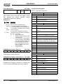
1
PRELIMINARY
ES1879
AudioDrive Solution
Data Sheet
®
DESCRIPTION
The ES1879 AudioDrive solution is a mixed-signal single-chip
solution that adds 16-bit stereo sound and FM music
synthesis to notebook computers. It is compliant with the
Microsoft PC97 specification and WHQL audio
requirements. The ES1879 includes an embedded
microcontroller, an OPL3™ superset ESFM™ music
synthesizer, 16-bit stereo wave CODEC, 16-bit stereo system
DAC, 16-bit stereo music DAC, 16-bit stereo I2S DAC,
optional ISA Plug and Play (PnP) support, hardware master
volume control, DMA control logic with FIFO, ISA bus
interface logic, general-purpose I/O, and digital dual game
port. The ES1879 also incorporates three serial ports that
allow interfacing with external DSP, wavetable, and MIDI
(MPU-401 UART mode compatible). In addition, the ES1879
offers I2S Zoom Video interface and support for the optional
ES978 Expansion Audio Mixer in docking stations.
A four-wire expansion analog bus and two-wire serial control
bus connect the ES1879 with the ES978, allowing the
ES1879 to engage the docking station’s audio resources
when docked.
The ES1879 AudioDrive can record, compress, and play back
voice, sound, and music with built-in mixer controls. Using two
high-performance DMA channels, the ES1879 supports fullduplex operation for simultaneous record and playback. One
channel supports bidirectional DMA data transfers and the
other supports DMA playback.
The ES1879 AudioDrive supports optional ISA Plug and Play
with configuration for 4 logical devices: configuration device,
audio plus ESFM™ synthesis, game port, and MPU-401.
The integrated 3-D audio effects processor uses technology
from Spatializer® Audio Laboratories, Inc. and expands the
sound field emitted by two speakers to create a resonant 3-D
sound environment.
The MPU-401 hardware is for interfacing with an external
MIDI serial port. The ES1879 music DAC allows the use of an
external wavetable (ES689/ES69x) connected to a wavetable
serial port. I/O address, DMA and interrupt selection can be
controlled through system software or Plug and Play.
Advanced Power Management (APM) features include
suspend and resume from disk.
The ES1879 is backward compatible and pin compatible with
the ES1878.
The ES1879 AudioDrive® solution is available in an industrystandard 100-pin Small Quad Flat Pack (SQFP) package.
FEATURES
Single, high-performance, mixed-signal, 16-bit stereo
VLSI chip for digital audio
High-quality, OPL3 superset ESFM™ music synthesizer
Patented ESPCM compression
High performance DMA supports Demand Transfer or
F-type
Integrated 3-D audio effects processor from Spatializer®
Record and Playback Features
Record, compress, and play back voice, sound, and
music
16-bit stereo CODEC for digital audio
3 additional stereo DACs for system playback, music
synthesis and I2S from PC card
Programmable sample rate from 4 kHz to 48 kHz for
record and playback
2- or 3-button hardware volume control for up, down, and
mute
Full-duplex stereo operation for simultaneous record and
playback
Inputs/Outputs
MIDI serial port compatible with MPU-401 UART mode
Supports up to 7 general-purpose inputs and 7 generalpurpose outputs that can be slaved with corresponding
pins of ES978 expansion audio mixer
ESS high performance dual game port with hardware
timing
A DSP serial interface in the ES1879 allows an external DSP
to take over ADC or DAC resources.
Optional full ISA Plug and Play support
I2S Zoom Video port interface with a sample rate up to 48
The ES1879 supports telegaming architecture with headsets
and includes data paths for host-based Acoustic Echo
Cancellation processing.
Wavetable serial port interface to ES689/ES69x for direct
kHz for MPEG audio
access to the music DAC
The enhanced dual game port supports hardware timing
interrupt generation that eliminates the need for CPU polling.
ESS Technology, Inc.
SAM0025A-062397
1
PRELIMINARY
ES1879 DATA SHEET
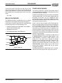
TYPICAL APPLICATION
Interfaces to Expansion Audio Mixer (ES978)
Power
Simple hot-docking interface to ES978 expansion audio
Advanced Power Management supports suspend/
mixer
resume from disk
Two-wire digital status and data communication between
ES1879 and ES978 supports register mirroring with
worst-case latency of approximately 140 µsec
Supports 3.3 or 5.0 V operation
Compatibility
Has on-chip dual pairs of analog differential signals for
Supports PC games in Sound Blaster™ and Sound
audio I/O with ES978 expansion audio mixer
Blaster™ Pro modes
Supports Microsoft Windows™ Sound System
Meets PC97 and WHQL specifications.
Mixer Features
6-channel stereo mixer inputs for line, auxiliary A (CD
audio), auxiliary B, digital audio (wave files), music
synthesizer, I2S Zoom Video plus a mono channel mixer
input for microphone
Programmable 6-bit logarithmic master volume control
Plug and Play (PnP) Features
On-chip Plug and Play support for audio, joystick port,
FM, and MPU-401
Operating Systems
Microsoft Windows95
Microsoft Windows™ 3.1
Microsoft Windows for Workgroups™
Microsoft Windows NT™ 3.51 & 4.0
IBM OS/2 Warp™
Software address mapping, four DMA and five IRQ
selections for motherboard implementation
Internal configuration data for audio Plug and Play
support
Read/Write serial interface for Plug and Play resource
EEPROM
TYPICAL APPLICATION
Notebook PC
Docking Station
Option
Line
Auxiliary
I2S Zoom Video
Line
Aux
Joystick
Mic
XA[3:0]
XSC
XSD
DOCKED
CD Audio
ES978
Speakers
Mic
ES1879
CD Audio
Speakers
I2S Zoom Video
Joystick
3-D Option
Wavetable Option
ES938
ES689/
ES69x
ISA Bus
Wavetable Option
ES689/
ES69x
2
SAM0025A-062397
ESS Technology, Inc.
ES1879 DATA SHEET
PRELIMINARY
CONTENTS
CONTENTS
DESCRIPTION . . . . . . . . . . . . . . . . . . . . . . . . . . . . . . . . . . . . 1
FEATURES . . . . . . . . . . . . . . . . . . . . . . . . . . . . . . . . . . . . . . . 1
Record and Playback Features . . . . . . . . . . . . . . . . . . . . 1
Inputs/Outputs . . . . . . . . . . . . . . . . . . . . . . . . . . . . . . . . . 1
Interfaces to Expansion Audio Mixer (ES978) . . . . . . . . . 2
Mixer Features . . . . . . . . . . . . . . . . . . . . . . . . . . . . . . . . . 2
Plug and Play (PnP) Features . . . . . . . . . . . . . . . . . . . . . 2
Power . . . . . . . . . . . . . . . . . . . . . . . . . . . . . . . . . . . . . . . 2
Compatibility . . . . . . . . . . . . . . . . . . . . . . . . . . . . . . . . . . 2
Operating Systems . . . . . . . . . . . . . . . . . . . . . . . . . . . . . 2
TYPICAL APPLICATION . . . . . . . . . . . . . . . . . . . . . . . . . . . . 2
CONTENTS . . . . . . . . . . . . . . . . . . . . . . . . . . . . . . . . . . . . . . 3
FIGURES . . . . . . . . . . . . . . . . . . . . . . . . . . . . . . . . . . . . . . . . 4
TABLES . . . . . . . . . . . . . . . . . . . . . . . . . . . . . . . . . . . . . . . . . 4
PINOUT . . . . . . . . . . . . . . . . . . . . . . . . . . . . . . . . . . . . . . . . . 5
PIN DESCRIPTION . . . . . . . . . . . . . . . . . . . . . . . . . . . . . . . . 6
FUNCTIONAL DESCRIPTION . . . . . . . . . . . . . . . . . . . . . . . . 8
Digital Subsystems . . . . . . . . . . . . . . . . . . . . . . . . . . . . . 8
Analog Subsystems . . . . . . . . . . . . . . . . . . . . . . . . . . . . . 9
MIXER SCHEMATIC BLOCK DIAGRAM . . . . . . . . . . . . . . . 10
TYPICAL APPLICATION . . . . . . . . . . . . . . . . . . . . . . . . . . . 11
ISA BUS INTERFACE . . . . . . . . . . . . . . . . . . . . . . . . . . . . . 12
DIGITAL AUDIO . . . . . . . . . . . . . . . . . . . . . . . . . . . . . . . . . . 12
Programming Data Transfers . . . . . . . . . . . . . . . . . . . . 12
First Audio Channel “CODEC” . . . . . . . . . . . . . . . . . . . . 14
DRQ LATCH FEATURE . . . . . . . . . . . . . . . . . . . . . . . . . . . . 15
FOURTH DRQ CHANNEL . . . . . . . . . . . . . . . . . . . . . . . . . . 15
INTERRUPTS . . . . . . . . . . . . . . . . . . . . . . . . . . . . . . . . . . . . 16
PERIPHERAL INTERFACING . . . . . . . . . . . . . . . . . . . . . . . 18
DSP Interface . . . . . . . . . . . . . . . . . . . . . . . . . . . . . . . . 18
I2S Serial Interface . . . . . . . . . . . . . . . . . . . . . . . . . . . . . 20
Wavetable Interface . . . . . . . . . . . . . . . . . . . . . . . . . . . . 20
MPU-401 Interface . . . . . . . . . . . . . . . . . . . . . . . . . . . . 20
Game/Joystick Interface . . . . . . . . . . . . . . . . . . . . . . . . 21
ES978 Interface . . . . . . . . . . . . . . . . . . . . . . . . . . . . . . . 22
Mono FDXI and FDXO . . . . . . . . . . . . . . . . . . . . . . . . . 25
General-Purpose I/O . . . . . . . . . . . . . . . . . . . . . . . . . . . 25
GPI/O Registers . . . . . . . . . . . . . . . . . . . . . . . . . . . . . . 25
Spatializer 3-D Audio Effects Processor . . . . . . . . . . . . 25
Master Volume . . . . . . . . . . . . . . . . . . . . . . . . . . . . . . . . 26
Hardware Volume Controls . . . . . . . . . . . . . . . . . . . . . . 26
PC Speaker . . . . . . . . . . . . . . . . . . . . . . . . . . . . . . . . . . 27
Serial EEPROM Interface . . . . . . . . . . . . . . . . . . . . . . . 27
ESS Technology, Inc.
ANALOG DESIGN CONSIDERATIONS . . . . . . . . . . . . . . . . 28
Reference Generator . . . . . . . . . . . . . . . . . . . . . . . . . . . 28
Switch-Capacitor Filter . . . . . . . . . . . . . . . . . . . . . . . . . . 28
Audio Inputs and Outputs . . . . . . . . . . . . . . . . . . . . . . . . 28
CONFIGURATION . . . . . . . . . . . . . . . . . . . . . . . . . . . . . . . . 29
Using ISA PnP Mode . . . . . . . . . . . . . . . . . . . . . . . . . . . 29
Non PnP Mode . . . . . . . . . . . . . . . . . . . . . . . . . . . . . . . . 29
Bypass Key . . . . . . . . . . . . . . . . . . . . . . . . . . . . . . . . . . 29
Accessing the ROM/EEPROM . . . . . . . . . . . . . . . . . . . . 30
PnP Configuration and Registers . . . . . . . . . . . . . . . . . . 30
Logical Device Registers . . . . . . . . . . . . . . . . . . . . . . . . 36
I/O PORTS . . . . . . . . . . . . . . . . . . . . . . . . . . . . . . . . . . . . . . . 41
Port Descriptions . . . . . . . . . . . . . . . . . . . . . . . . . . . . . . 41
PROGRAMMING THE ES1879 . . . . . . . . . . . . . . . . . . . . . . . 47
Identifying the ES1879 . . . . . . . . . . . . . . . . . . . . . . . . . . 47
Resetting the Audio Device via Software . . . . . . . . . . . . 47
Modes of Operation . . . . . . . . . . . . . . . . . . . . . . . . . . . . 47
Data Formats . . . . . . . . . . . . . . . . . . . . . . . . . . . . . . . . . 48
Compatibility Mode Programming . . . . . . . . . . . . . . . . . 50
Extended Mode Programming . . . . . . . . . . . . . . . . . . . . 52
Programming the ES1879 Mixer . . . . . . . . . . . . . . . . . . 59
REGISTERS . . . . . . . . . . . . . . . . . . . . . . . . . . . . . . . . . . . . . 62
Types of Register Access . . . . . . . . . . . . . . . . . . . . . . . . 62
AUDIO MICROCONTROLLER COMMAND SUMMARY . . . 84
POWER MANAGEMENT . . . . . . . . . . . . . . . . . . . . . . . . . . . 87
Power Management Characteristics . . . . . . . . . . . . . . . 87
BIOS Power Management . . . . . . . . . . . . . . . . . . . . . . . 87
ELECTRICAL CHARACTERISTICS . . . . . . . . . . . . . . . . . . . 89
Absolute Maximum Ratings . . . . . . . . . . . . . . . . . . . . . . 89
Thermal Characteristics . . . . . . . . . . . . . . . . . . . . . . . . . 89
Operating Conditions . . . . . . . . . . . . . . . . . . . . . . . . . . . 89
DC Electrical Characteristics . . . . . . . . . . . . . . . . . . . . . 89
Power Management Characteristics . . . . . . . . . . . . . . . 90
ES1879 TIMING DIAGRAMS . . . . . . . . . . . . . . . . . . . . . . . . 91
TIMING CHARACTERISTICS . . . . . . . . . . . . . . . . . . . . . . . . 95
MECHANICAL DIMENSIONS . . . . . . . . . . . . . . . . . . . . . . . . 96
APPENDIX A: ES1879 INTERNAL PNP RESOURCE ROM 97
APPENDIX B: ES689/ES69X DIGITAL SERIAL INTERFACE 99
APPENDIX C: I2S ZV INTERFACE REFERENCE . . . . . . . 100
APPENDIX D: SCHEMATIC EXAMPLES . . . . . . . . . . . . . . 105
APPENDIX E: LAYOUT GUIDELINES . . . . . . . . . . . . . . . . 109
APPENDIX F: ES1879 BILL OF MATERIALS . . . . . . . . . . . 110
SAM0025A-062397
3
PRELIMINARY
ES1879 DATA SHEET
FIGURES
FIGURES
Figure 1 ES1879 Pinout . . . . . . . . . . . . . . . . . . . . . . . . . . . . .5
Figure 2 ES1879 Functional Block Diagram . . . . . . . . . . . . . .8
Figure 3 ES1879 Mixer Schematic Block Diagram . . . . . . . .10
Figure 4 ES1879 Typical Application . . . . . . . . . . . . . . . . . . 11
Figure 5 Data Transfer Modes . . . . . . . . . . . . . . . . . . . . . . .12
Figure 6 DRQ Latch . . . . . . . . . . . . . . . . . . . . . . . . . . . . . . .15
Figure 7 DSP Operating Modes . . . . . . . . . . . . . . . . . . . . . .18
Figure 8 16-Bit Data, Positive Sync Pulse . . . . . . . . . . . . . .19
Figure 9 I2S Implementation in ES1879 . . . . . . . . . . . . . . . .20
Figure 10 Dual Joystick/MIDI Connector . . . . . . . . . . . . . . . .21
Figure 11 MIDI Serial Interface Adapter . . . . . . . . . . . . . . . .22
Figure 12 PC Speaker Volume Circuitry . . . . . . . . . . . . . . . .27
Figure 13 Serial EEPROM – Typical Application . . . . . . . . .27
Figure 14 Reference Generator Pin Diagram . . . . . . . . . . . .28
Figure 15 Switch-Capacitor Filter Pin Diagram . . . . . . . . . . .28
Figure 16 Configuration Register Outline . . . . . . . . . . . . . . .30
Figure 17 Command Transfer Timing . . . . . . . . . . . . . . . . . .49
Figure 18 Reset Timing . . . . . . . . . . . . . . . . . . . . . . . . . . . . .91
Figure 19 I/O Read Cycle . . . . . . . . . . . . . . . . . . . . . . . . . . .91
Figure 20 I/O Write Cycle . . . . . . . . . . . . . . . . . . . . . . . . . . .91
Figure 21
Figure 22
Figure 23
Figure 24
Figure 25
Figure 26
Figure 27
Figure 28
Figure 29
Figure 30
Figure 31
Figure 32
Figure 33
Figure 34
Figure 35
Figure 36
Figure 37
Figure 38
Compatibility Mode DMA Write Cycle . . . . . . . . . 92
Compatibility Mode DMA Read Cycle . . . . . . . . . 92
Serial Mode Receive Operation . . . . . . . . . . . . . . 93
Serial Mode Transmit Operation . . . . . . . . . . . . . 93
Serial Input Timing for I2S Interface . . . . . . . . . . . 94
I2S Digital Input Format with 16 SCLK Periods . . 94
ES1879 Physical Dimensions . . . . . . . . . . . . . . . 96
MIDI Interface Data Format . . . . . . . . . . . . . . . . . 99
Example ZV Port Implementation . . . . . . . . . . . 100
Typical ZV Port Audio Implementation . . . . . . . 101
Audio Interface Timing . . . . . . . . . . . . . . . . . . . . 102
I2S Digital Input Format with 16 SCLK Periods . 103
ES1879 Schematic . . . . . . . . . . . . . . . . . . . . . . 105
PC Interface . . . . . . . . . . . . . . . . . . . . . . . . . . . . 106
Amplifier Section . . . . . . . . . . . . . . . . . . . . . . . . 107
Switch and Connector Section . . . . . . . . . . . . . 108
Analog Components on One Side of the PCB . . 109
Analog Components on Both Sides of the PCB. 109
TABLES
Table 1 ES1879 ISA Bus Interface . . . . . . . . . . . . . . . . . . . .12
Table 2 ES1879 Interrupt Sources . . . . . . . . . . . . . . . . . . . .16
Table 3 DSP Interface Pins . . . . . . . . . . . . . . . . . . . . . . . . . .18
Table 4 Digital Audio Mixing Methods in Serial Mode . . . . . .19
Table 5 I2S Interface Pins . . . . . . . . . . . . . . . . . . . . . . . . . . .20
Table 6 Wavetable Interface Pins . . . . . . . . . . . . . . . . . . . . .20
Table 7 Digital Joystick Read Values . . . . . . . . . . . . . . . . . .21
Table 8 ES978 Interface Pins . . . . . . . . . . . . . . . . . . . . . . . .22
Table 9 Docked Modes for Analog Audio . . . . . . . . . . . . . . .23
Table 10 Download Period Data Configuration . . . . . . . . . . .24
Table 11 Upload Period Data Configuration . . . . . . . . . . . . .25
Table 12 Resource Assignment . . . . . . . . . . . . . . . . . . . . . .35
Table 13 Logical Device Summary . . . . . . . . . . . . . . . . . . . .36
Table 14 I/O Ports for Configuration, Audio, FM, MPU-401, and
Joystick Devices . . . . . . . . . . . . . . . . . . . . . . . . . . . . . . . . . . .41
Table 15 Comparison of Operation Modes . . . . . . . . . . . . . .48
Table 16 Uncompressed DAC Transfer Modes . . . . . . . . . . .50
Table 17 Uncompressed ADC Transfer Modes . . . . . . . . . . .51
Table 18 Command Sequences for DMA Playback . . . . . . .53
Table 19 Command Sequences for DMA Record . . . . . . . . .55
4
SAM0025A-062397
Table 20 Sound Blaster Pro/Extended Access Registers . . 59
Table 21 Mixer Input Volume Registers . . . . . . . . . . . . . . . . 61
Table 22 SB Pro Read Volume Emulation . . . . . . . . . . . . . . 61
Table 23 SB Pro Write Volume Emulation . . . . . . . . . . . . . . 61
Table 24 Sound Blaster Pro-Compatible Register Summary 62
Table 25 ESS Mixer Register Summary . . . . . . . . . . . . . . . 63
Table 26 Test Bus Assignments . . . . . . . . . . . . . . . . . . . . . . 78
Table 27 ESS Controller Registers Summary . . . . . . . . . . . 79
Table 28 Command Summary . . . . . . . . . . . . . . . . . . . . . . . 84
Table 29 Power Mode Description . . . . . . . . . . . . . . . . . . . . 87
Table 30 Digital Characteristics . . . . . . . . . . . . . . . . . . . . . . 89
Table 31 Analog Characteristics
(VDDA = 5.0 V ± 5%; TA = 25 °C) . . . . . . . . . . . . . . . . . . . . 89
Table 32 Current Consumption for Power Modes . . . . . . . . 90
Table 33 Common Clock Frequencies . . . . . . . . . . . . . . . . 100
Table 34 AC Parameters for Audio Signals . . . . . . . . . . . . 102
Table 35 ZV Port Interface Pin Assignments . . . . . . . . . . . 104
Table 36 ES1879 Bill of Materials (BOM) . . . . . . . . . . . . . 110
ESS Technology, Inc.
PRELIMINARY
ES1879 DATA SHEET
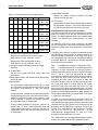
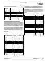
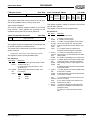
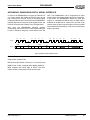
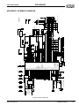
PINOUT
77
78
79
80
81
82
83
84
85
86
87
ES1879S
88
89
90
91
92
93
94
95
96
97
98
99
51
52
54
55
56
57
53
50
49
48
47
46
45
44
43
42
41
40
39
38
37
36
35
34
33
32
31
30
29
28
27
26
1
2
3
4
5
6
7
8
9
10
11
12
13
14
15
16
17
18
19
20
21
22
23
24
25
100
58
59
60
61
62
63
64
65
66
67
68
69
70
71
72
73
76
PCSPKO
AOUT_R
AOUT_L
LINE_R
LINE_ L
CIN_R
CIN_L
FOUT_L
FOUT_R
VDDA
CAP3D
GNDA
MIC
CMR
AUXA_R
AUXA_L
AUXB_R/FDXO
AUXB_L/FDXI
TA
TB
TC
TD
S WA
SWB
SWC
GNDD
A0
A1
A2
A3
A4
A5
A6
A7
A8
A9
A10
A 11
AEN
VDDD
D0
D1
D2
D3
D4
D5
D6
D7
GNDD
SWD
XO
PCSPKI
GNDD
GPI0
DRQD / GPI1
GPO0
GPO1
SECLK / GPO2
DRQC / GPI2
DACKBC / GPI3
DRQB
DACKBB
DRQA
DACKBA
DACKBD / MUTE / GPI4
SEDI / VOLUP / GPI5
SEDO / VOLDN / GPI6
IRQE / GPO6
IRQD / GPO5
IRQC / GPO4
IRQB / GPO3
IRQA
IORB
IOWB
VDDD
74
75
XI
VDDD
RESET
DOCKED
SECS
IILR
IISCLK
I I D ATA
MSD
MCLK
FS
DCLK
DR
DX
GNDD
MSI
MSO
IPROM
XSC
XSD
GNDA
XA0
XA1
XA2
XA3
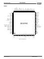
PINOUT
Figure 1 ES1879 Pinout
ESS Technology, Inc.
SAM0025A-062397
5
PRELIMINARY
ES1879 DATA SHEET
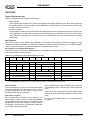
PIN DESCRIPTION
PIN DESCRIPTION
Name
GNDD
A[11:0]
AEN
VDDD
D[7:0]
SW(A-D)
T(A-D)
AUXB_L
FDXI
AUXB_R
FDXO
AUXA_L,
AUXA_R
CMR
MIC
GNDA
CAP3D
VDDA
FOUT_L,
FOUT_R
CIN_L,
CIN_R
LINE_L,
LINE_R
AOUT_L,
AOUT_R
PCSPKO
XA[3:0]
Number
1, 24, 61, 78
13:2
14
15, 74, 100
23:16
28:25
32:29
I/O
I
I
I
I
I/O
I
I/O
Description
Digital ground.
ISA address bus.
ISA address valid when active-low, DMA when high.
Digital power supply (3.0 - 5.5 V).
ISA data bus. 24 mA drivers.
Joystick switch inputs. These pins have internal pull-ups to VDDD.
Joystick timers. Use the digital power supply. These pins have internally weak pull-downs
to GNDD (> 1M Ω).
Aux B input, left. 50k Ω pull-up to CMR.
Used with DSP interface as line-level mono input (25k Ω input impedance).
Aux B input, right. 50k Ω pull-up to CMR.
Used with DSP interface as line-level mono output, capable of driving a 5k Ω load.
Aux A (CD) inputs, left and right. 50k Ω pull-ups to CMR.
35,36
I
I
I
O
I
37
38
39, 55
40
41
43:42
O
I
I
O
I
O
44, 45
I
2.25 V reference buffer output.
Mic input to +26 dB internal preamp. 80k Ω pull-up to CMR.
Analog ground.
Bypass capacitor to GNDA for 3-D effect.
Analog power supply, 4.75 - 5.25 V.
Filter outputs, left and right. These pins are normally AC coupled to CIN_L and CIN_R.
The output resistance is about 5k Ω.
Capacitive coupled inputs, left and right. The input resistance is about 50k Ω.
46, 47
I
Line inputs, left and right. 50k Ω pull-ups to CMR.
48, 49
O
Analog outputs, left and right, from master volume. These pins can drive a 5k Ω load.
50
51, 52, 53, 54
O
I/O
GNDA
XSD
XSC
IPROM
55
56
57
58
I
I/O
O/Hi Z
I
MSO
MSI
DX
59
60
62
O
I
O/Hi Z
DR
DCLK
FS
63
64
65
I
I
I
MCLK
MSD
IIDATA
IISCLK
IILR
66
67
68
69
70
I
I
I
I
I
PC speaker analog output.
Bidirectional differential transmitter/receivers. Expansion audio bus. These are analog signals that are DC-coupled to the corresponding pins of the ES978.
Analog ground.
Expansion serial bus data I/O. High-impedance when DOCKED = 0.
Expansion serial bus clock and frame sync. High-impedance when DOCKED = 0.
Select between internal PnP ROM and external EEPROM for Plug and Play configuration.
1 = internal ROM, 0 = external EEPROM. ES1878 function PNPEN is replaced by bit 2 of
PnP Vendor register 2Dh.
MIDI serial output.
MIDI serial input. MSI has an internal pull-up to VDDD.
Serial data transmit. Active output when data is being transmitted serially from the
ES1879; otherwise, high impedance. Tri-state output.
Serial data receive. This pin has an internal pull-down to GNDD.
Serial clock input. This pin has an internal pull-down to GNDD.
Frame sync input. Software-programmable to be active-high or active-low. This pin has
an internal pull-down to GNDD.
Serial clock input from ES689/ES69x. This pin has an internal pull-down to GNDD.
Serial data input from ES689/ES69x. This pin has an internal pull-down to GNDD.
Serial data for I2S interface. This pin has an internal pull-down to GNDD.
Serial shift clock for I2S interface. This pin has an internal pull-down to GNDD. I2S
Left/right signal for I2S interface. This pin has an internal pull-down to GNDD.
6
33
34
SAM0025A-062397
ESS Technology, Inc.
PRELIMINARY
ES1879 DATA SHEET
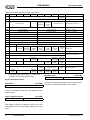
PIN DESCRIPTION
Name
SECS
Number
71
I/O
I
DOCKED
72
I
RESET
XI
XO
PCSPKI
GPI0
DRQD
GPI1
GPO[1:0]
GPO2
SECLK
DRQC
GPI2
DACKBC
GPI3
DRQB
DACKBB
DRQA
DACKBA
DACKBD
MUTE
GPI4
SEDI
VOLUP
GPI5
SEDO
VOLDN
GPI6
IRQE
GPO6
IRQD
GPO5
IRQC
GPO4
IRQB
GPO3
IRQA
IORB
IOWB
73
75
76
77
79
I
I
O
I
I
O/Hi Z
I
O
O
I
O/Hi Z
I
I
I
O/Hi Z
I
O/Hi Z
I
I
I
I
I
I
I
O
I
I
O/Hi Z
O
O/Hi Z
O
O/Hi Z
O
O/Hi Z
O
O/Hi Z
I
O
80
82:81
83
84
85
86
87
88
89
90
91
92
93
94
95
96
97
98
99
ESS Technology, Inc.
Description
Serial EEPROM CS. This pin is an input during reset when IRPOM = 1. It is No-Connect
when IRPOM = 0.
ROM Type
IRPOM SECS
0
1
93LC66, 512×8, 9 address bits.
1
x
Internal mask ROM.
Status input that is active-high when the ES1879 is docked to the ES978. This pin has an
internal pull-down to GNDD.
ISA active-high reset.
14.31818 MHz clock input, or external crystal.
Output to external 14.31818 MHz crystal.
PC speaker digital input. This pin has an internal pull-down.
General-purpose input 0.
ISA active-high DMA request.
General-purpose input 1.
General-purpose outputs.
General-purpose outputs when SECS = 0.
External serial EEPROM clock pin for PnP when SECS = 1.
ISA active-high DMA request.
General-purpose input 2.
ISA active-low DMA acknowledge.
General-purpose input 3.
ISA active-high DMA request.
ISA active-low DMA acknowledge.
ISA active-high DMA request.
ISA active-low DMA acknowledge.
ISA active-low DMA acknowledge.
Active-low mute input. This pin has an internal pull-up to VDDD.
Optionally used as general-purpose input 4.
Data input pin to external PnP serial EEPROM when SECS = 1.
Active-low volume-up input. This pin has an internal pull-up to VDDD.
Optionally used as general-purpose input 5.
Data output pin to external PnP serial EEPROM when SECS = 1.
Active-low volume-down input. This pin has an internal pull-up to VDDD.
Optionally used as general-purpose input 6.
ISA interrupt request. 16 mA driver.
General-purpose output 6.
ISA interrupt request. 16 mA driver.
General-purpose output 5.
ISA interrupt request. 16 mA driver.
General-purpose output 4.
ISA interrupt request. 16 mA driver.
General-purpose output 3.
ISA interrupt request. 16 mA driver.
ISA active-low read strobe.
ISA active-low write strobe.
SAM0025A-062397
7
PRELIMINARY
ES1879 DATA SHEET
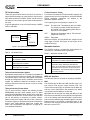
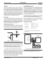
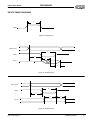
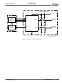
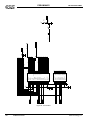
FUNCTIONAL DESCRIPTION
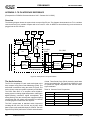
FUNCTIONAL DESCRIPTION
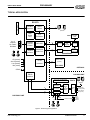
This section shows the overall structure of the ES1879
and discusses its major functional subunits.
GNDD
The major subunits of the ES1879 are shown in Figure 2
and are briefly described in the following paragraphs.
GPI[6:0]* GPO[6:0]* PCSPKI
CIN FOUT
VDDD
VOL CTRL
PREAMP
MIC
GENERAL
PURPOSE I/O
FILTER
LINE
AUXA
AUXB*
FDXI/O*
1-BIT
DAC
PCSPKO
A[11:0]
D[7:0]
16-BIT
IRQ(A-E)*
FIFO
STEREO
ISA
DRQ(A-D)*
BUS
DACKB(A-D)*
DAC
GNDA
RECORD
MIXER
VDDA
RECORD
SOURCE
AND
VOLUME
CONTROL
PLAYBACK
MIXER
INTERFACE
AND
REGISTER
SET
16-BIT
IOWB
IORB
RESET
FIFO
STEREO
CODEC
AEN
IPROM
CAP3D
3-D
ROM
XA[3:0]
DSP
ANALOG
DR
SERIAL
I/F
ESFM
ES689/ES69x
I2S ZV
SERIAL PORT
FS
PORT
DCLK
DOCKED
ES978
VOLUP*
MASTER
VOL
CTRL
™
16-BIT
STEREO DAC
16-BIT
STEREO DAC
AOUT
VOLDN*
DX
MICROCONTROLLER
RAM
ES978
SERIAL PORT
OSCILLATOR
MPU-401
SERIAL PORT
DUAL GAME
SERIAL PORT
DIGITAL
XSC
I/F
XSD
REF GEN
MUTE*
IILR
IISCLK
IIDATA
XI
XO
MSD MCLK
MSI
MSO SW(A-D) T(A-D)
CMR
* Some of these pins are shared with other functions.
Figure 2 ES1879 Functional Block Diagram
Digital Subsystems
RISC microcontroller – game-compatible audio
functions are performed by an embedded microcontroller.
Oscillator – circuitry to support an external crystal.
ROM and RAM – firmware ROM and data RAM to the
embedded microcontroller.
FIFO – RAM for a 256-byte FIFO data buffer for use with
the first audio channel and RAM for a 64-byte FIFO for
use with the second audio channel.
ISA bus interface – provides interface to ISA bus
address, data, and control signals.
Digital dual game port – ESS high-performance digital
switches for two joysticks with hardware timing.
8
SAM0025A-062397
ES978 digital interface – allows support for ES978
Expansion Audio Mixer in the docking station. Two wires
transmit and receive control signals and a thrid wire
reports the docking status.
I2S Zoom Video serial port – supports sample rates up
to 48 kHz for MPEG audio.
MPU-401 serial port – asynchronous serial port for MIDI
devices such as a wavetable synthesizer or a music
keyboard input.
Wavetable serial port – serial port connection from the
output of an ES689 or ES69x that eliminates the need for
an external DAC.
DSP serial port – interface for an optional external DSP
for control of the CODEC.
ESS Technology, Inc.
PRELIMINARY
ES1879 DATA SHEET
FUNCTIONAL DESCRIPTION
ESFM™ music synthesizer – high-quality OPL3
superset FM synthesizer.
3-D Processor – Spatializer technology 3-D audio effects
Recording source and input volume control – input
source and volume control for record. The recording
source can be selected from one of seven choices:
– Mic
processor.
Hardware volume control – three pushbutton inputs
– Line
with internal pull-up devices for up/down/mute can be
used to adjust the master volume control.
– Aux A (CD)
The state of these pins is logically AND’d with the state
of the corresponding pins of the ES978 when docked.
A software-selectable option allows the mute input to
be omitted. The mute input is defined as the state when
both up and down inputs are low. By default, this
feature is disabled.
– Playback Mixer – master volume inputs (outputs of
the Spatializer processor, but before master volume
is applied).
The hardware volume inputs of the ES1879 can be
used as general-purpose inputs (see bits 4 and 5 of
Vendor-Defined Card-Level register 25h). They cannot
be used as volume control inputs.
Analog Subsystems
Stereo programmable record and playback mixers –
seven input stereo mixers. Each input has independent
left and right 4-bit volume control.
– Line In
– Mic In
– Aux A (CD)
– Playback Mixer – AOUT_L/AOUT_R (after master
volume has been applied).
– Mic/master volume inputs mix. Left channel: Mic
(not mixed with ES978 mic), Right channel: master
volume inputs left and right.
In any of the first four cases, the selected recording
source may be mixed with audio from the ES978 if the
selected source is also enabled in the ES978 and the
two chips are docked.
Master volume and mute control – the master volume
is controlled by either Programmed I/O or volume control
switch inputs. The master volume supports 6 bits per
channel plus mute. When docked, the ES1879 first
transmits the master volume information to the ES978
mixer before it can take effect.
ES978 analog interface – allows support for ES978
– Aux B (or FDXI)
– Digital audio (wave files)
– FM/ES689/ES69x music DAC
– I2S serial port DAC
16-Bit stereo CODEC – for audio record and playback
CODEC.
16-Bit stereo system DAC – for audio playback of the
second audio channel.
Expansion Audio Mixer in the docking station. The fourwire differential analog bus carries audio data between
the ES978 and the ES1879. Audio data from the ES978
is input to the mixer of the ES1879. A switch determines
whether audio data transmitted to the ES978 is taken
before or after master volume is applied.
Reference generator – analog reference voltage
generator.
16-Bit stereo music DAC – for ESFM™ or external
wavetable synthesizer.
16-Bit Stereo I S DAC – I S Zoom Video for MPEG audio
2
– Record Mixer
2
DAC.
1-Bit DAC – for PC speaker digital input.
PC speaker volume control – the PC speaker is
supported with a 1-bit DAC with volume control. The
analog output pin PCSPKO is intended to be externally
mixed at the external amplifier. PC speaker audio is not
transmitted to the ES978 through the expansion audio
interface (XA[3:0]). The ES1879 is designed to play PC
speaker audio through the speakers inherent to the
portable unit.
General-purpose I/O – Seven general-purpose inputs
and outputs which can be slaved with the corresponding
pins of the ES978 Expansion Audio Mixer.
Filter – switched capacitor low-pass filter.
Preamp – 26 dB microphone preamplifier.
ESS Technology, Inc.
SAM0025A-062397
9
PRELIMINARY
ES1879 DATA SHEET
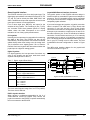
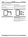
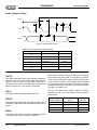
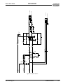
MIXER SCHEMATIC BLOCK DIAGRAM
MIXER SCHEMATIC BLOCK DIAGRAM
ADC/DAC
DMA 1
Output
Volume
digital audio
DAC
DMA 2
digital audio
DAC
I2S/ZV
I2S/ZV
MPEG audio
Preamp
MIC
Playback
Mixer
LINE
Spatializer
3-D
DOCKED
On
DAC
FM/
HWWT
ES978
Off
AUXA
Record
Monitor
Off
AUXB
Record
Source
ES978
ES978
Volume
On
Σ
Mute
Master
Volume
AOUT
Σ
Record
Volume
Input
Volume
ADC
Record
Mixer
Mute
Figure 3 ES1879 Mixer Schematic Block Diagram
10
SAM0025A-062397
ESS Technology, Inc.
PRELIMINARY
ES1879 DATA SHEET
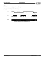
TYPICAL APPLICATION
TYPICAL APPLICATION
ISA BUS
ES1879
2 or 3
Buttons
Up, Down,
and Mute
ISA Bus
Interface
AOUT
Stereo
DSP
Serial
Port
3-D
Processor
Hardware
Volume
Control
Joystick
Controls
CD (stereo)
Aux B (stereo)
Line (stereo)
Mic (mono)
L
R
Speakers
1-Mbyte
Wavetable
ROM
ES981
MPU-401
2
MIDI
Serial Port
Wavetable
Audio Port
2
Serial
Port
General
MIDI
Interpreter
Wavetable
Synthesizer
Chorus &
Reverb
(ES69x only)
ES689/ES69X
I2S ZV
MPEG Audio
(I2S ZV)
3
Interface
PC CARD
OPTIONAL
GPI/O
DOCKING UNIT
ES978
Interface
I2S ZV Port or ES689/ES69x
Wavetable Serial Port
Oversampling
Stereo DAC
2
Differential
Transceiver
4
Digital
Controller
Record
&
Playback
Mixers
ES978
Analog
I/O
L
R
Speakers
CD (stereo)
Aux B (stereo)
Line (stereo)
Mic (mono)
PORTABLE UNIT
MIDI
GPI/O
Volume Control
Joysticks
2 or 3
Buttons
Up, Down,
and Mute
Figure 4 ES1879 Typical Application
ESS Technology, Inc.
SAM0025A-062397
11
PRELIMINARY
ES1879 DATA SHEET
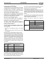
ISA BUS INTERFACE
ISA BUS INTERFACE
Table 1 shows the pins used to interface the ES1879 with the ISA bus.
Table 1 ES1879 ISA Bus Interface
Pin
I/O
A[11:0]
I
AEN
I
Description
ISA address bus.
ISA address valid when active-low, DMA when high.
D[7:0]
I/O
ISA data bus. 24 mA drivers.
IOWB
O
ISA active-low write strobe.
IORB
I
ISA active-low read strobe.
IRQ(A-E)
O/Hi Z
ISA interrupt request. 16 mA driver.
I
ISA active-low DMA acknowledge.
DACKB(A-D)
DRQ(A-D)
O/Hi Z
RESET
I
ISA active-high DMA request.
ISA active-high reset.
DIGITAL AUDIO
The ES1879 incorporates two audio channels:
Programming Data Transfers
Audio 1 The first audio channel. This channel is used for
Sound Blaster Pro-compatible DMA, Extended
mode DMA, and Programmed I/O. It can be
used for either record or playback. This channel
can be mapped to any of the three 8-bit ISA
DMA channels: 0, 1, or 3.
Programming Data transfers can be quite complicated
with the ES1879. Both Compatibility mode and Extended
mode offer a variety of modes for conducting transfers.
The commands to enable the different transfers varies
depending on which audio channel is used and which
mode (Compatibility or Extended) is used.
Audio 2 The second audio channel. This channel is used
for audio playback in full-duplex mode. This
channel can be mapped to any of the three 8-bit
ISA DMA channels or the 16-bit channel.
The biggest difference in available data transfer modes is
between audio channel 1 and audio channel 2. This is
illustrated in Figure 5. Audio 2 allows only for DMA mode.
Audio 1 allows for Direct mode and DMA mode when
using Compatibility mode. Audio 1 allows for Programmed
I/O and DMA mode when using Extended mode.
The two DMA sources are mapped to the four DMA pin
pairs through PnP registers. Also, the four DMA pin pairs
are assigned ISA DMA channel numbers by VendorDefined Card-Level registers 23h and 24h.
Digital Audio
In order for a DRQ output pin to be driving (as opposed to
high-impedance), two things must occur:
1. The PnP register for the DMA of a given device
must match the ISA DMA channel number of the
pin.
2. The given device must be activated (that is, bit 0 of
PnP register 30h must be high).
For detailed information, see “PnP Configuration and
Registers” .
Figure 5 Data Transfer Modes
12
SAM0025A-062397
Audio 1
Compatibility
Mode
Direct
Mode
DMA
Mode
Audio 2
Extended
Mode
Programmed
I/O
DMA
Mode
DMA
Mode
Data Formats
See “Data Formats” on page 48.
ESS Technology, Inc.
ES1879 DATA SHEET
PRELIMINARY
DIGITAL AUDIO
Data Transfers in Compatibility Mode
The first audio channel can be programmed using the
standard Sound Blaster-compatible commands. These
commands are written to the chip through port
Audio_Base+Ch.
When programming the first audio channel for
Compatibilty mode transfers one of the following modes
can be used:
Direct Mode
DMA Mode
– Normal
– Auto-Initialize
In addition, both Normal DMA mode and Auto-Initialize
DMA mode can use a special High-Speed mode.
Direct Mode
In Direct mode, the timing for DMA transfers is handled by
the application program. For example, the system timer
can be reprogrammed to generate interrupts at the
desired sample rate. At each system timer interrupt, the
command 10h, 11h, 20h, or 21h is issued, followed by the
sample. Polling of the write buffer available flag
(Audio_Base+Ch [bit 7]) is required before writing the
command and between the command and the data.
NOTE: The switched capacitor filter is initialized by reset
for an intended sample rate of 8 kHz. In Direct mode, the
application may try to adjust this filter appropriate to the
actual sample rate. The easiest way to do this is to
program the timer with command 40h just as if the
application were using DMA mode.
Normal DMA Mode
In Normal mode DMA transfers, the DMA controller must
be initialized and the ES1879 must be commanded for
every block that is transferred.
Auto-Initialize DMA Mode
In Auto-Initialize mode, the DMA transfer is continuous, in
a circular buffer, and the ES1879 generates an interrupt
for the transition between buffer halves. In this mode, the
DMA controller and ES1879 need to be set up only once.
High-Speed Mode
The ES1879 supports mono 8-bit DMA transfers at a rate
of up to 44 kHz. Mono 16-bit transfers are supported up to
a rate of 22 kHz.
There is a special High-Speed mode” that allows 8-bit
sampling up to 44 kHz for ADC. This mode uses
commands 98h (Auto-Initialization) and 99h (Normal). No
automatic gain control (AGC) is performed. The input
volume is controlled with command DDh.
Data Transfers in Extended Mode
The first audio channel is programmed using the controller
registers internal to the ES1879. The commands written to
the controller registers are written to the chip through port
Audio_Base+Ch.
When programming the first audio channel for transfers,
one of the following modes can be used:
Programmed I/O
DMA mode:
DMA Mode
– Normal (Single or Demand transfer)
In DMA mode, the programmable timer in the ES1879
controls the rate at which samples are sent to the CODEC.
The timer is programmed using command 40h, which also
sets up the programmable filters inside the ES1879. The
ES1879 firmware maintains an internal FIFO (32 levels for
16-bit transfers, 64 levels for 8-bit transfers) that is filled by
DMA transfers and emptied by the timed transfers to the
DAC.
– Auto-Initialize (Single or Demand transfer)
Before a DMA transfer, the application first programs the
DMA controller for the desired transfer size and address,
then programs the ES1879 with the same size
information. At the end of the transfer, the ES1879
generates an interrupt request, indicating that the current
block transfer is complete. The FIFO gives the application
program sufficient time to respond to the interrupt and
initiate the next block transfer.
The ES1879 supports both Normal DMA mode and AutoInitialize DMA mode.
ESS Technology, Inc.
In addition, both DMA Normal mode and DMA AutoInitialize mode use Single transfer or Demand transfer
mode.
Programmed I/O
For some applications, DMA mode is not suitable or
available for data transfer, and it is not possible to take
exclusive control of the system for DAC and ADC
transfers. In these situations, use I/O block transfers within
an interrupt handler. The REP OUTSB instruction of the
80x86 family transfers data from memory to an I/O port
specified by the DX register. The REP INSB instruction is
the complementary function. Use ES1879 port
Audio_Base+Fh for block transfers.
I/O transfers to FIFO are nearly identical to the DMA
process, except that an I/O access to port
Audio_Base+Fh replaces the DMA cycle. For details
about Programmed I/O, operation see “Extended Mode
Programmed I/O Operation” on page 55.
SAM0025A-062397
13
PRELIMINARY
ES1879 DATA SHEET
DIGITAL AUDIO
DMA Mode
Extended mode DMA supports both Normal and AutoInitialize mode. In addition, Normal mode and AutoInitialize mode both support Single and Demand transfer
modes.
Using Single transfer, one byte is transferred per DMA
request. Demand transfer reduces the number of DMA
requests necessary to make a transfer by allowing two or
four bytes to be transferred per DMA request. Thus there
are multiple DMA acknowledges for each DMA request.
For a description of DMA mode including Normal DMA
mode and Auto-Initialize DMA mode see “DMA Mode” on
page 13.
Extended Mode Audio 1 Controller Registers
The following registers control operation of the first audio
channel in Extended mode:
Address
A1h
A2h
A4h
A5h
B1h
B2h
B4h
B5h
B6h
B7h
B8h
B9h
Name
Audio 1 Sample Rate Generator register
Audio 1 Filter Clock Divider register
Audio 1 Transfer Count Reload register – low byte
Audio 1 Transfer Count Reload register – high byte
Audio Interrupt Control register
Audio 1 DRQ Control register
Input Volume Control register
Audio 1 DAC Direct Access register – low byte
Audio 1 DAC Direct Access register – high byte
Audio 1 Control 1 register
Audio 1 Control 2 register
Audio 1 Transfer Type register
Data Transfers Using the Second Audio Channel
The second audio channel is programmed using mixer
registers 70h through 7Ah. The commands written to the
mixer registers are written to the chip through ports
Audio_Base+4h and Audio_Base+5h.
DMA mode is used when programming the second audio
channel for transfers:
DMA mode:
– Normal (Single or Demand transfer)
– Auto-Initialize (Single or Demand transfer)
In addition, both DMA Normal mode and DMA AutoInitialize mode use Single transfer or Demand transfer
modes.
DMA Mode
DMA under the second audio channel supports both
Normal and Auto-Initialize modes. In addition, Normal
mode and Auto-Initialize mode both support Single and
Demand transfer modes.
14
SAM0025A-062397
Using Single transfer, one byte is transferred per DMA
request. Demand transfer reduces the number of DMA
requests necessary to make a transfer by allowing two,
four, or eight bytes to be transferred per DMA request.
Thus there are multiple DMA acknowledges for each DMA
request.
For a description of DMA mode including Normal DMA
mode and Auto-Initialize DMA mode, see “DMA Mode” on
page 13.
Audio 2 Related Mixer Registers
The following registers control DMA operations for the
second audio channel:
Address Name
70h
Audio 2 Sample Rate Generator register
72h
Audio 2 Filter Clock Divider register
74h
Audio 2 Transfer Count Reload register – low byte
76h
Audio 2 Transfer Count Reload register – high byte
78h
Audio 2 Control 1 register
7Ah
Audio 2 Control 2 register
First Audio Channel “CODEC”
The CODEC of the first audio channel is not a true stereo
CODEC in that it cannot perform stereo DAC and ADC
simultaneously. The first audio channel CODEC can be
either a stereo DAC, a stereo ADC, or a mono CODEC.
After reset, the CODEC is set up for DAC operations. Any
ADC command causes a switch to the ADC “direction” and
any subsequent DAC command switches the converter
back to the DAC “direction.”
The DAC output is filtered and input to the mixer. After
reset, input to the mixer from the first audio channel DAC
is muted. This is to prevent pops. The ES1879 maintains
a status flag to determine if the input to the mixer from the
first audio channel DAC is enabled or disabled. The
command D8h returns the status of the flag (00h =
disabled and FFh = enabled). Use command D1h to
enable input to the mixer from the first audio channel DAC
and command D3h to disable the input.
To play a new sound without resetting beforehand when
the status of the analog circuits is not clear, mute the input
to the mixer with command D3h, then set up DAC direction
and level using the direct-to-DAC command:
10h + 80h
Wait 25 msec for the analog circuitry to settle before
enabling the input to the mixer with command D1h.
ESS Technology, Inc.
PRELIMINARY
ES1879 DATA SHEET
DRQ LATCH FEATURE
A pop may be heard if the DAC level was left at a value
other than mid-level (code 80h on an 8-bit scale) by the
previous play operation. To prevent this, always finish a
DAC transfer with a command to set the DAC level to midrange:
10h + 80h
DRQ LATCH FEATURE
The DRQ latch feature is enabled when bit 7 of VendorDefined Card-Level register 29h is high (see Figure 6).
If this feature is enabled, each of the four audio DRQs will
be latched high until one of the following occurs:
A DACK low pulse occurs while DRQ is low or if DRQ
goes low due to a DACK pulse.
A hardware reset occurs.
8-16 milliseconds elapse while DRQ is low.
DRQ
125 Hz
-DACK
OR
S
S
R
R
AND
-RESET
DRQ Out
FOURTH DRQ CHANNEL
The ES1879 supports an optional fourth DMA channel
using pins DRQD and DACKBD. Connecting these pins to
an ISA DMA channel is optional.
If DRQD and DACKBD are not connected to an ISA DMA
channel, program bits 7:4 of PnP Vendor register 24h to be
2h (0010). In this case, pin 80 is available as GPI1
(general-purpose input 1) and pin 90 is available as either
the active-low hardware volume control MUTE input or as
GPI4 (general-purpose input 4).
If bits 7:4 of PnP Vendor register 24h are other than 2h,
then pin 80 is assumed to be connected to an ISA DRQ pin
and is not available as GPI1 (if GPI1 is read, it appears to
be 1 all the time). Likewise, pin 90 is assumed to be
connected to an ISA DACK pin and is not available to be
used as a hardware volume MUTE input or GPI4. If a mute
function is desired, program mixer register 64h so that the
combination of both VOLUP and VOLDN pins low together
acts as a mute command.
Normally, DRQA/DACKBA is connected to DMA channel
0, DRQB/DACKBB is connected to DMA channel 1, and
DRQC/DACKBC is connected to DMA channel 3. This
leaves one of the three 16-bit channels for DRQD/
DACKBD. Since the ES1879 only has 8 data lines, the
Windows driver will arrange the data so that a 16-bit
channel can be used for 8-bit data. For this reason, the
DRQD/DACKBD channel should only be used for the
second DAC playback channel and not the gamecompatible first channel.
Figure 6 DRQ Latch
The DRQ latch feature is enabled when bit 7 of VendorDefined Card-Level register 29h is high (see Figure 6).
ESS Technology, Inc.
SAM0025A-062397
15
PRELIMINARY
ES1879 DATA SHEET
INTERRUPTS
INTERRUPTS
There are four interrupt sources in the ES1879:
Table 2 ES1879 Interrupt Sources
Interrupt Source
Description
Audio 1
This interrupt is used for the first audio channel (Sound Blaster-compatible DMA, Extended mode DMA, and
Extended mode Programmed I/O), as well as SB-compatible (Sound Blaster-compatible) MIDI receive. This
interrupt request is cleared by a hardware or software reset, or by an I/O read from Audio_Base+Eh. The
interrupt request can be polled by reading from Audio_Base+Ch. This interrupt is assigned to an interrupt
channel by PnP register 70h of LDN 1 (Logical Device Number 1).
Audio 2
Optional for the second DMA channel. The ES1879 can operate in full-duplex mode using two DMA channels.
However, the second DMA channel must have the same sample rate as the first DMA channel. For this reason, it is not necessary to use a separate interrupt for the second DMA channel. This interrupt is masked by
bit 6 of mixer register 7Ah. It can be polled and cleared by reading or writing bit 7 of the same register. This
interrupt is assigned to an interrupt channel by PnP register 72h of LDN 1.
Hardware Volume
This interrupt occurs when one of the three hardware volume controls generates an event. Bit 1 of mixer register 64h is the mask bit for this interrupt. The interrupt request can be polled by reading bit 3 of the
same register. The interrupt request is cleared by writing any value to register 66h. This interrupt is
assigned to an interrupt channel by PnP register 28h. Typically this interrupt, if used, is shared with
an audio interrupt.
MPU-401
This interrupt occurs when a MIDI byte is received. It will go low when a byte is read from the MIDI FIFO and
go high again quickly if there are additional bytes in the FIFO. The interrupt status is the same as the Read
Data Available status flag in the MPU-401 Status register. This interrupt is masked by bit 6 of mixer reg-
ister 64h and is assigned to an interrupt channel in one of two ways: If the MPU-401 is part of the
audio device, then PnP register 28h is used to assign the MPU-401 interrupt. If the MPU-401 is its
own logical device, it can also be assigned to an interrupt via PnP register 70h of LDN 3. Both of
these methods access the same physical register.
Interrupt Sources
Interrupt sources are mapped to any one of the five
interrupt output pins via the PnP registers. A given pin can
have zero, one, or more interrupts mapped to it. Each PnP
pin is assigned to an ISA interrupt channel number by
Vendor-Defined Card-Level PnP registers 20h, 21h, and
22h. These registers are automatically loaded from the 8byte header in the PnP configuration data.
If a given interrupt pin has one or more sources assigned
to it, and one or more of those sources is activated
(register 30h, bit 0), then the interrupt pin will be active;
that is, it will always be driving high or low. Each interrupt
also has one or more mask bits that are AND'd with the
interrupt request.
Interrupt Status Register (ISR)
Port Config_Base+6h of the configuration device can be
read to quickly find the current state of ES1879 interrupt
sources. The following bits describe the state of the
ES1879 interrupt sources:
16
Bit 3
MPU-401 receive interrupt request AND’d
with bit 6 of mixer register 64h
Bit 2
Hardware volume interrupt request AND’d
with bit 1 of mixer register 64h
SAM0025A-062397
Bit 1
Audio 2 interrupt request AND’d with bit 6 of
Mixer Extension register 7Ah
Bit 0
Audio 1 interrupt request
Interrupt Mask Register (IMR)
Register 7h of the configuration device can be used to
mask any of the four interrupt sources.
The mask bits can be used to force the interrupt source to
be zero, but they do not put the interrupt pin in a highimpedance state. Each bit is AND’d with the
corresponding interrupt source. This port is set to all ones
on a hardware reset.
The Interrupt Status Register (ISR) is not affected by the
state of the Interrupt Mask Register (IMR). That is, the ISR
reflects the status of the interrupt request lines before
being masked by the IMR.
The IMR is useful when interrupts are shared. For
example, assume that audio 1, audio 2, hardware volume,
and MPU-401 all share the same interrupt in Windows.
When returning from Windows to DOS, the hardware
volume, MPU-401, and Audio 2 interrupts can be masked
by setting the appropriate bits to 0.
ESS Technology, Inc.
ES1879 DATA SHEET
PRELIMINARY
INTERRUPTS
A second use of the IMR is within an interrupt handler. The
first thing the interrupt handler can do is mask all of the
interrupt sources mapped to the interrupt handler. The ISR
can then be polled to decide which sources to process.
Just before exiting the interrupt handler, the IMR can be
restored. If an unprocessed interrupt remains active, it
generates an interrupt request because the interrupt pin
was low during the masked period and then went high
when the interrupt sources were unmasked. While the
interrupts are masked, the individual interrupt sources can
change state any number of times without generating a
false interrupt request.
Interrupt Edge Generator
The interrupt logic has a feature that makes sharing of
interrupts easier. If more than one interrupt source shares
an interrupt request pin, the interrupt pin is normally the
logical OR of the shared interrupt requests. However, if
any one interrupt request goes from high to low, circuitry
inside the ES1879 will hold the interrupt request pin low
briefly to generate a clock edge if one of the other interrupt
sources is also high.
Sharing Interrupts
Plug and Play does not support sharing of interrupts in its
resource assignment decision making. If a device tries to
share an interrupt with another device that has been
assigned an interrupt by PnP, the first device cannot
request an interrupt for itself.
A logical device that supports interrupts can be assigned
to an interrupt after the PnP sequence is generated by the
Windows driver. In this case, the logical device would
typically be forced to share an interrupt with the first audio
interrupt. For most cases, this is done simply by
programming the appropriate PnP register (70h or 72h) for
the selected device.
A special case is the hardware volume interrupt. This
interrupt source can be assigned to an interrupt through
Vendor-Defined Card-Level register 28h, bits 7:4.
A second special case is the MPU-401 interrupt. The
MPU-401 device is either part of the audio device or its
own logical device. If it is part of the audio device, the
interrupt can be assigned by writing to Vendor-Defined
Card-Level register 28h, bits 3:0. If the MPU-401 device is
its own logical device, it is assigned an interrupt by either
Vendor-Defined Card-Level register 28h or LDN 3 register
70h.
ESS Technology, Inc.
SAM0025A-062397
17
PRELIMINARY
ES1879 DATA SHEET
PERIPHERAL INTERFACING
PERIPHERAL INTERFACING
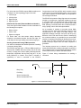
DSP Interface
Telegaming Mode
The ES1879 contains a synchronous serial interface for
connection to a DSP serial interface. The typical
application for this interface is a speakerphone.
This mode is enabled when two conditions are present:
Table 3 DSP Interface Pins
Bit 0 of mixer register 48h is high. This bit enables
The DSP serial port must be enabled (i.e., bit 7 of Mixer
register 48h is high).
Telegaming mode.
Pin
Description
DCLK
Data clock input. The rate can vary, but a typical
value is 2.048 MHz (8 kHz x 256). Input with pulldown.
DX
Data transmit. Active output when data is being
transmitted serially from the ES1879; otherwise,
high impedance. Tri-state output.
DR
Serial data input with pull-down.
FS
Frame sync input for transmit. Software-programmable to be active-high or active-low. Input with
pull-down.
DSP Operating Modes
There are two DSP data transfer modes for the ES1879.
The state of a single switch internal to the ES1879
determines which mode is enabled. This switch can route
the first audio channel to the second audio channel DAC.
When the first audio channel is routed to the second audio
channel DAC, Telegaming mode is enabled. Otherwise,
the DSP is operating in its default mode.
In earlier chips, when the DSP serial port is enabled, the
Audio 1 CODEC is unavailable for use by the first audio
channel. This means digital audio for Sound Blaster Procompatible games is muted. Sound Blaster can use only
the first audio channel for digital audio. The Audio 1
CODEC is used by the DSP.
In Telegaming mode, the first audio channel can be
switched over to the Audio 2 DAC. Internally, the first audio
channel is routed to the second audio channel DAC and
the second audio channel has no function. In addition, the
second audio channel mixer volume control is slaved to
the first audio channel mixer volume control.
Default Mode
The default mode operates just like telegaming mode
except that data from the first audio channel cannot be
heard. Data sent through the second audio channel can be
mixed as in Telegaming mode.
No Acoustic Echo Cancellation
The DSP cannot perform acoustic echo cancellation in
either mode. Because the audio from the host does not
pass directly through the DSP, there is no way for the DSP
to compensate for acoustic echo. Therefore, using a
headset for either the microphone or speakers or both is
recommended.
16-bit Stereo DAC
16-bit Stereo DAC
DAC
DAC
DMA2
FIFO
16-bit Stereo
CODEC
ISA
Bus
DAC
ADC
DAC
ADC
DMA1
FIFO
Serializer/
Deserializer
DAC
DAC
DMA2
FIFO
Microphone
FDXO
Mixer
16-bit Stereo
CODEC
ISA
Bus
DAC
ADC
DAC
ADC
DMA1
FIFO
Speaker
DSP/CODEC
Port
Serializer/
Deserializer
Microphone
FDXO
Mixer
Speaker
DSP/CODEC
Port
Telegaming Mode
Default Mode
Figure 7 DSP Operating Modes
18
SAM0025A-062397
ESS Technology, Inc.
PRELIMINARY
ES1879 DATA SHEET
PERIPHERAL INTERFACING
DSP Digital Audio Playback
Mixing External to the ES1879
There are two choices for mixing the DSP digital audio
playback data with other audio sources. The audio data
can be mixed in the ES1879’s internal playback mixer or
external to the ES1879.
The second method is to use the FDXO output pin and mix
the DSP digital audio playback and the game-compatible
digital audio playback in an external audio mixer. To select
this method, set the Output Signal Control bits of Mixer
register 44h for mixer output except DAC playback. To do
this, program bits 6:4 of register 44h to 1, 0, and 1,
respectively. In addition, set bit 1 of Mixer register 46h high
to enable FDXO as an output when DSP serial mode is
enabled.
Mixing Internal to the ES1879
The DSP digital audio playback can be mixed within the
ES1879 playback mixer. To select this method, set the
Output Signal Control bits of the Mixer register 44h for
mixer output. To do this, program bits 6:4 of mixer register
44h to 1, 0, and 0, respectively. The volume of the DSP
digital audio playback is controlled by the DAC Play
Volume register 14h.
The volume of the DSP digital audio playback is controlled
within the DSP by scaling the data.
NOTE: In Telegaming mode, register 14h also controls
the game-compatible first audio channel digital audio
playback. If independent mixer volume control of the
game-compatible and DSP digital audio data is
necessary, use the second method.
Table 4 Digital Audio Mixing Methods in Serial Mode
To mix DSP and digital
audio...
...set the Output Signal
Control bits of register
44h to...
...and the volume of the DSP
digital audio playback is
controlled by...
In addition...
Bit 6
Bit 5
Bit 4
internal to the ES1879
1
0
0
DAC Play Volume register 14h
N/A
external to the ES1879
1
0
1
scaling the data within the DSP
set bit 1 of register 46h high.
DSP Interface Serial Data Format
DCLK
FS
DX
Hi-Z
D15
D14
D13
D12
D1
D14
D13
D12
D1
D0
(MSB)
DR
D15
D0
(MSB)
Figure 8 16-Bit Data, Positive Sync Pulse
ESS Technology, Inc.
SAM0025A-062397
19
PRELIMINARY
ES1879 DATA SHEET
PERIPHERAL INTERFACING
I2S Serial Interface
Three input pins, IIDATA, IISCLK, and IILR, are used for a
serial interface between an external device and a stereo
DAC within the ES1879. IIDATA, IISCLK, and IILR can be
left floating or connected to ground if the serial interface is
not used.
2
A typical applications of the I S serial interface is MPEG
audio or CD audio.
I2S Serial Interface Timing
This section discusses the I2S serial interface signals. The
signals when the port is configured for use with an ES689/
ES69x wavetable synthesizer are defined in the
Wavetable Interface section.
Three signals (plus one optional) are used for I2S:
IISCLK
The shift clock. The maximum rate is 6.4 MHz.
The minimum number of IISCLK periods per
IILR period is 32. Any number greater than or
equal to 32 is acceptable.
IILR
Sample synchronization signal. The maximum
sample rate is 50 kHz.
IISCLK
IIDATA
Serial data.
IILR
Within the ES1879, IILR and IIDATA are sampled on the
rising edge of IISCLK. See Figure 25 and Figure 26 for
detailed I2S timing.
IIDATA
PC CARD
ES1879
Figure 9 I2S Implementation in ES1879
Wavetable Interface
The ES1879 contains a synchronous serial interface for
connection to a wavetable music synthesizer.
.
Table 5 I2S Interface Pins
Table 6 Wavetable Interface Pins
Pin
Description
IIDATA
Serial data for I2S interface. This pin has an internal pull-down to GNDD.
IISCLK
Serial shift clock for I2S interface. This pin has an
internal pull-down to GNDD.
IILR
Left/Right signal for I S interface. This pin has an
internal pull-down to GNDD.
2
I2S Serial Interface Software Enable
By hardware reset default, the I2S interface is disabled. Bit
6 of Vendor-Defined Card-Level register 29h enables the
I2S interface when it is set high. This register is accessed
through the configuration device. In addition, bit 6 of mixer
register 71h enables the data bus connection to the I2S
interface. Both these bits must be set in order to enable
the interface.
I2S Serial Interface Format Select
The I2S serial interface supports two different formats:
ES689/ES69x two-wire serial interface and I 2S. When
used in the ES689/ES69x format, IIDATA is the serial data
and IISCLK is the bit clock. The IILR input is not used and
can be left floating or connected to ground. VendorDefined Card-Level register 29h bits 5 and 4 select the
format (this register is accessed through the configuration
device). See Vendor-Defined Card-Level register 29h
under “PnP Configuration and Registers” on page 30 for
more detailed information.
20
SAM0025A-062397
Pin
Description
MCLK
Serial clock from external ES689/ES69x music
synthesizer (2.75 MHz). Input with pull-down.
MSD
Serial data from external ES689/ES69x music
synthesizer. When both MCLK and MSD are
active, the stereo DACs normally used by the FM
synthesizer are acquired for use by the external
ES689/ES69x. The normal FM output is blocked.
Input with pull-down.
MPU-401 Interface
The MPU-401 port can be used for interfacing with MIDI.
MIDI
The ES1879 has an MPU-401 MIDI interface with a 23byte receive FIFO and an 8-byte transmit FIFO. The
output of the transmit FIFO is serialized out the MSO pin
and also sent to the ES978 in the expansion unit, where
it is serialized out the MSO pin of that chip.
MIDI data can be received from either the MSI pin of the
ES1879 or from the MSI pin of the ES978 in the expansion
unit. In the unlikely event that MIDI data is received from
both sources simultaneously, the data might be corrupted.
Data received by the ES978 is transmitted back to the
ES1879 in the next upload frame and then placed in the
MPU-401 receive FIFO.
ESS Technology, Inc.
ES1879 DATA SHEET
PRELIMINARY
PERIPHERAL INTERFACING
Game/Joystick Interface
The ES1879 includes 8 pins for a dual joystick port. The
digital game port address is decoded for timer pins TA, TB,
TC, and TD, and for switch pins SWA, SWB, SWC, and
SWD. The MIDI serial input and output also come from the
game port connector in most applications.
Four of these eight pins, SW(A-D), are inputs
switches of the joysticks. The remaining 4 pins,
are "one-shot" timers that generate pulses of
widths, where the width corresponds to the
resistance of one of the joystick potentiometers.
for the
T(A-D),
varying
current
PC Joysticks
Normally, the host processor is responsible for measuring
the width of the pulse. The ES1879 can also do this
automatically. The host processor can read the measured
widths directly rather than having to do the timing itself.
This is referred to as a “digital joystick.” Bit 1 of VendorDefined Card-Level register 29h determines whether the
joystick port is a digital or analog joystick.
Digital Joysticks
For digital joysticks, the host processor first writes any
value to the joystick port and then reads back seven
separate values (shown in Table 7).
Table 7 Digital Joystick Read Values
Joystick/MIDI External Interface Connector
The joystick portion of the ES1879 reference design is
identical to that on a standard PC game control adapter or
game port. The PC-compatible joystick can be connected
to a 15-pin D-sub connector. It supports all standard PCcompatible joystick software.
If you need to support two joysticks, a joystick conversion
cable is required. This cable uses a 15-pin D-sub male
connector on one end and two 15-pin D-sub female
connectors on the other end. All signals on this cable have
direct pin-to-pin connection, except for pins 12 and 15. On
the male connector, pins 12 and 15 should be left without
connection. On the female connector, pin 15 is internally
connected to pin 8, and pin 12 is internally connected to
pin 4. The dual joystick port and MIDI port take up only one
slot in your PC, leaving room for other cards. The dual
joystick/MIDI connector configuration is shown in Figure
10.
The MIDI serial interface adapter for the joystick/midi
connector is shown in Figure 11.
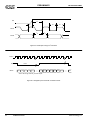
+5V
Joystick B
Joystick A
9
X-axis
10
1
2
X-axis
3
Read #1
Low byte timer A
Read #2
Low byte timer B
Read #3
Low byte timer C
Button
11
12
Button
13
14
Y-axis
15
Read #4
Low byte timer D
Read #5
Bits 3:0 – Upper nibble timer A
Bits 7:4 – Upper nibble timer B
Read #6
Bits 3:0 – Upper nibble timer C
Bits 7:4 – Upper nibble timer D
Read #7
Bit 0 – switch A
Bit 1 – switch B
Bit 2 – switch C
Bit 3 – switch D
MIDI OUT
MIDI IN
4
Button
5
6
Button
7
8
Y-axis
GND
Figure 10 Dual Joystick/MIDI Connector
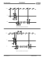
The timer values reported range from 0 to FFFh (0-4095).
The timer clock is 895 kHz.
ES978 Joystick Interface
When docked, a software-programmable bit (bit 0 of
Vendor-Defined Card-Level register 29h) causes the
joystick connected to the ES978 to replace automatically
the one connected to the ES1879f.
ESS Technology, Inc.
SAM0025A-062397
21
PRELIMINARY
ES1879 DATA SHEET
PERIPHERAL INTERFACING
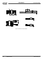
JOYSTICK PORT
8
15
7
14
6
13
5
12
4
11
3
10
2
9
1
R3
220
R4
2.2K
R1
10K
Q1
2N3904
R2
270
Q2
2N3904
R5
5.6K
C1
220pF
C2
220pF
5
3
2 4
1
DIN
J1
MIDI OUT
R6
270
D1
DB15P
ISO1
5
3
MIDI IN
2 4
1
DIN
J2
Figure 11 MIDI Serial Interface Adapter
ES978 Interface
When docked, the ES1879 is in constant communication
with the ES978 in the expansion unit. A half-duplex,
bidirectional serial link keeps each chip updated on the
status of the other. For example, the status of the mixer
registers located in the ES1879 are transmitted down to
the ES978. MIDI data received in the ES978 is transmitted
up to the ES1879.
In addition to the digital control link, four analog wires
connect the two chips directly. These four wires are
configured as a pair of differential audio channels. The
ES1879 uses these two audio channels in one of four
ways: stereo playback (ES1879 transmits to the ES978),
stereo record (the ES978 transmits to the ES1879), mono
full-duplex (one mono channel in each direction), and
stereo full-duplex (one stereo channel in each direction).
Table 8 ES978 Interface Pins
Pin
Description
XA[3:0]
Bidirectional differential transmitter/receivers.
Expansion audio bus. These are analog signals
that are DC-coupled to the corresponding pins of
the ES978.
XSD
Expansion serial bus data I/O. High-impedance
when DOCKED = 0.
XSC
Expansion serial bus clock and frame sync. Highimpedance when DOCKED = 0.
DOCKED
Status input that is active-high when the ES1879
is docked to the ES978. This pin has an internal
pull-down to GNDD.
22
SAM0025A-062397
This interface uses six wires: two analog ground wires and
four analog signal wires (XA[3:0]). The four signal wires
are used in one of five different modes. In each of these
modes, the master always refers to the ES1879 and the
slave always refers to the ES978.
Mode 0 – Stereo playback. Two differential pairs for left
and right channels, transmitted from the master to the
slave.
Mode 1 – Stereo record. Two differential pairs for left and
right channels, transmitted from the slave to the master.
Mode 2 – Monophonic full-duplex. Two differential pairs.
One pair is for monophonic playback from master to
slave, the second pair is for monophonic recording from
slave to master. The mono playback signal is input to both
left and right host audio inputs of the playback mixer. The
mono record signal is derived by averaging the left and
right outputs of the record mixer.
Mode 3 – Stereo full-duplex. The four signals are not used
differentially ( This mode is not supported by the
ES1878).
Mode 4 – Not docked (DOCKED=0). Like Mode 0, except
the analog outputs follow AOUT_L and AOUT_R rather
than the output of the mixer.
After a change of mode, the data is muted at the receiving
end for a period of 25 milliseconds. It is the responsibility
of the master not to have contention caused by both ends
transmitting on the same signal wire.
ESS Technology, Inc.
PRELIMINARY
ES1879 DATA SHEET
PERIPHERAL INTERFACING
Table 9 shows the mode configurations when the
notebook unit is docked.
Table 9 Docked Modes for Analog Audio
Mode XA0
XA1
XA2
XA3
0
-Left Play
+Left Play
-Right Play
+Right Play
1
+Left
Record
-Left
Record
+Right
Record
-Right
Record
2
-Play
+Play
+Record
-Record
3
Left Record Left Play
Right Record Right Play
Docking Status
The ES1879 is either in docked or undocked state. The
state is determined by the DOCKED input, which is activehigh when docked.
In the undocked state, the XSC and XSD pins are driven
low. The XA[3:0] pins act as in mode 0 (differential
outputs), except they follow the AOUT_L/AOUT_R
outputs directly (i.e., after the master volume).
Playback Mode
The ES1879/ES978 design assumes that the active
speakers move from the portable to the expansion unit
when docked. Except when recording, expansion audio
sources are mixed in the expansion unit within the ES978
and played through speakers in the expansion unit. In
most cases, speakers within the portable unit are
programmed to be automatically muted when docked.
An exception is PC speaker beeps, which are always
heard in the portable, even when docked.
Each audio input can be programmed individually on how
to respond to a docking situation in one of the three ways:
As an analog input, such as mic, that remains in the
portable (ES1879) when docked and is muted in the
ES978.
As an analog input, such as line-in, that is disabled in the
ES1879 when docked and enabled in the ES978 when
docked, i.e., it is muted in the mixers in the ES1879 and
ES978.
As an analog input that is enabled in both the ES1879 and
ES978 mixers, and shares a common volume control.
(Note: An exception to sharing a common volume control
is allowed for the Mappable Volume register 5Dh; see
below).
The playback master volume is controlled through
software programming or by the up/down/mute switch
inputs. The latter method, called hardware volume control,
has active-low switch inputs in both the ES1879 and
ES978.
ESS Technology, Inc.
Record Mode
In record mode, the expansion audio bus is turned around,
and sound data is sent from the expansion unit ES978
chip to the ES1879 in the portable unit. The sound data
from the expansion unit can be mixed inside the ES1879
with local sources before recording. Because portable unit
sources (for example, FM) can be mixed into the
recording, it is not possible to do a record monitor function
through the expansion unit speakers (they are
automatically muted in record mode). It is possible for the
record monitor to use the speakers in the portable unit
(see bit 5 of Vendor-Defined Card-Level register 2Bh.)
The default situation for most applications is to have all
speakers muted during recording.
As in previous chips, one of four record sources can be
selected: Mic, Line, Aux A, or Mixer. When docked, the
ES1879 chip knows whether each resource is present in
the portable, the docking station, or both, and acts
accordingly.
Mono Full-Duplex Mode
In the ES1879, host-based software applications can use
full-duplex mode through two 8-bit DMA channels. The
restriction is that both record and playback are
monophonic.
The record channel can record from any analog input of
the ES1879, any analog input of the remote ES978, any
mix of the same, or from the FDXI input to the ES1879
when using the DSP serial port.
Stereo Full-Duplex Mode
In the ES1879, host-based software applications can use
stereo full-duplex mode through two 8-bit DMA channels.
The record channel can record from any analog input of
the ES1879, any analog input of the remote ES978, or any
mix of the same. It is possible to record from the FDXI
input to the ES1879 when using the DSP serial port, but
this data is monophonic.
No ES978 – Differential AOUT Mode
In some applications, there is no ES978 in the expansion
unit. In this case, XA[3:0] are used as differential outputs
that follow AOUT_L/AOUT_R and are intended to connect
to a differential-input power amplifier in the expansion unit.
This mode of operation is selected automatically
whenever the DOCKED input is zero. When DOCKED is
zero, XSC and XSD are high-impedance.
Power Management
Power management is controlled by bits 1:0 of VendorDefined Card-Level register 2Dh. In previous AudioDrive®
chips, power management was controlled via I/O port
SAM0025A-062397
23
PRELIMINARY
ES1879 DATA SHEET
PERIPHERAL INTERFACING
Audio_Base+7h. Only bit 5 (FM reset) and bit 7 (suspend
request) of I/O port Audio_Base+7h are supported in the
ES1879.
Expansion Audio Interface – Digital
Two wires are used to transmit serial data between the
ES1879 and ES978. The first signal, XSC, acts as a frame
sync and shift clock. The bit clock rate is 3.58 MHz.
Table 10 contains the data configuration for the download
period.
Table 10 Download Period Data Configuration
Byte
Bits
Function
0
1:0
4:2
5
6
7
Mode of expansion analog interface
Record source select
Master output enable
1: MIDI loopback test
1: MIDI transmit signal (byte 1 contains
MIDI data)
1
15:8
MIDI transmit data (if bit 7 of byte 0 is high)
2
23:16
XGPO[7:0] data
3
31:24
Playback mixer – Host audio volume
4
39:32
Playback mixer – Line volume
5
47:40
Playback mixer – Mic volume
6
55:48
Playback mixer – Aux A (CD) volume
7
63:56
Playback mixer – Aux B volume
8
71:64
Playback mixer – I2S/ES689 volume
9
79:72
Reserved
A typical frame consists of:
Sync period – 24 clocks wide
Download period – 144 clocks wide
Turnaround period – 8 clocks wide
Upload period – 80 clocks wide
Total: 256 bit clocks/frame, which is equivalent to a 14 kHz
frame rate.
The function of the upload and download periods is to
continually update corresponding registers within each
device. For example, pressing the VOLUP button in the
expansion unit, transmits the pin state to the ES1879
where it is AND’d with the same pin of the ES1879. The
ES1879 updates its copy of the master volume register.
The ES978 receives the new value in the master volume
register during the first download period of the next frame.
10
87:80
Record mixer – Line volume
11
95:88
Record mixer – Mic volume
12
103:96
Record mixer – Aux A (CD) volume
13
111:104
Record mixer – Aux B volume
Sync Period
14
119:112
Record mixer – I2S/ES689 volume
In the sync period, XSC is low for 12 bit clock periods, and
then high for 12 bit clock periods.
15
126:120
127
Master volume left
1: Mute left
Download Period
16
134:128
135
Master volume right
1: Mute right
17
143:136
CRC checksum
In the download period, data is transmitted serially from
the ES1879 to the ES978 via the signal XSD. XSC is the
bit shift clock. Data is shifted out of the ES1879 on the
falling edge of XSC. Data is shifted into the ES978 on the
rising edge of XSC.
The download period is 144 bits wide. Each bit takes 4
oscillator clocks (bit rate = 3.58 MHz). The last 8 bits are a
checksum byte.
The upload period is 80 bits wide. The last 8 bits are a
checksum byte.
24
SAM0025A-062397
Turnaround Period
There are 8 bits between the end of the download period
and the start of the upload period.
Upload Period
In the upload period, data is transmitted serially in the
opposite direction, from the ES978 to the ES1879 via the
same signal wire, XSD.
ESS Technology, Inc.
ES1879 DATA SHEET
PRELIMINARY
PERIPHERAL INTERFACING
Table 11 contains the data configuration for the upload
period.
Table 11 Upload Period Data Configuration
Byte
0
Bits
Function
3:0
4
5
6
7
Joystick switch status
VOLUP input status
VOLDN input status
MUTE input status
1: MIDI receive data following
1
15:8
MIDI receive data if bit 7 of byte 0 is set.
2
23:16 XGPI input state
3
31:24 Low byte joystick timer A
4
39:32 Low byte joystick timer B
5
47:40 Low byte joystick timer C
6
55:48 Low byte joystick timer D
7
59:56 High nibble joystick timer A
63:60 High nibble joystick timer B
8
67:64 High nibble joystick timer C
71:68 High nibble joystick timer D
9
79:72 CRC checksum
Expansion Audio Interface – Analog
Mono FDXI and FDXO
FDXI is shared with AUXB_L and FDXO is shared with
AUXB_R. The ES1879 supports the use of FDXI and
FDXO as input to the ADC and output from the DAC when
using the DSP serial port.
Mono FDXI/O mode is useful with an external modem that
has integrated a CODEC for speakerphone applications.
Bits 1:0 of Mixer Extension register 46h enable FDXI as a
mono input and FDXO as a mono output. When FDXI is a
mono input to the mixer, its input impedance is cut in half
to 25k ohms. When FDXO is an output, it has a 5k ohm
output impedance. When FDXO is not an output, it is the
AUXB_R input to the mixer and has a 50k ohm pull-up to
CMR.
Each enabled GPI input can be read by the host processor
at any time. Also, each GPI input can be programmed to
remotely control a corresponding GPO output in the
ES978, thereby saving interconnects between the
portable and expansion units.
Each enabled GPO pin can be controlled either by a write
by the host to an ES1879 register or remotely from a
corresponding GPI pin of the ES978.
The worst-case latency between the ES978 and ES1879,
due to the serial interconnection, is about 140 µsec.
GPI/O Registers
The GPI/O registers are as follows:
Configuration_Device_Base+2h
Bits 6:0 of this register set the state of the GPO[6:0]
pins that are enabled as outputs and are not mapped
to the GPI pins of the ES978.
Configuration_Device_Base+3h
Bits 7:0 of this register set the state of the XGPO[7:0]
pins of the ES978 that are not mapped to the GPI pins
of the ES1879.
Vendor-Defined Card-Level register 25h
This register controls whether any shared function pins
are general-purpose inputs/outputs.
Vendor-Defined Card-Level register 26h
Vendor-Defined Card-Level register 26h, which is the
GPO Map register, selects whether a GPO pin is
controlled by Configuration_Device_Base+2h or by the
GPI pin of ES978.
Vendor-Defined Card-Level register 27h
Vendor-Defined Card-Level register 27h, which is the
GPI Map register, selects whether a GPI pin controls a
XGPO pin in the ES978, or if the XGPO pin is
controlled by Configuration_Device_Base+3h.
Contact an ESS Field Application Engineer for an
application note on how to use the FDXI/FDXO feature.
NOTE: Bits 1 and 0 of register Audio_Base+7h do not
control GPO0 and GPO1 as in previous AudioDrive® chips.
Also, the feature of previous audio controllers that causes
GPO0 and GPO1 to change state automatically when the
chip is powered down is not supported in the ES1879.
General-Purpose I/O
Spatializer 3-D Audio Effects Processor
Up to seven general-purpose inputs and seven generalpurpose outputs are available. Four of the GPO pins have
another function (ISA interrupt request output) and may
not be available for use as general-purpose outputs. All of
the GPI pins have other functions (volume control, DRQC,
DACKBC, DRQD, DACKBD) and may not be available for
use as general-purpose inputs. For more information, see
“GPI/O Registers” .
The ES1879 incoporates an embedded Spatializer audio
effects processor, positioned between the output of the
playback mixer and the master volume controls. The
Spatializer produces a wider perceived stereo effect.
Given a mono input, the Spatializer processor has a mode
that generates a stereo effect.
ESS Technology, Inc.
SAM0025A-062397
25
PRELIMINARY
ES1879 DATA SHEET
PERIPHERAL INTERFACING
The amount of effect can be controlled by either directly
programming mixer register 52h or by allowing the
ES1879 to control the effect level automatically, based on
the stereo content of the input signal. This latter feature is
called auto-limiting. In auto-limiting, the ES1879
constantly adjusts the amount of effect based on the
stereo content of the input signal. The host software can
set a maximum effect level by programming register 52h.
This gives the auto-limiting logic an upper bound.
Master Volume
The master volume is controlled through Programmed I/O
or volume control switch inputs. The master volume
supports 6 bits per channel plus mute. When docked, the
ES1879 transmits the master volume information to the
ES978 where it takes effect after the output of the ES978
mixer.
For support of legacy master volume control, any write to
legacy mixer register 22h or 32h is translated
automatically into writes to the master volume registers.
Since mixer register 22h only has 3-bit resolution and
mixer register 32h only 4-bit resolution, a translation circuit
is included in the ES1879 that translates 3- or 4-bit volume
values into the 6-bit volume plus mute that is used by the
master volume registers. Reading a legacy master volume
register (22h or 32h) also uses a translation circuit to
convert 6-bit master volumes plus mute into 3- or 4-bit
legacy master volume numbers. Support of legacy mixer
registers can be defeated under software control.
See also “Programming the ES1879 Mixer” on page 59.
Hardware Volume Controls
VOLUP, VOLDN, and MUTE are three input pins with
internal pull-up devices. The state of these pins is AND’d
with the state of the corresponding pins of the ES978
when docked.
The VOLUP and VOLDN buttons produce a single-step
change in volume when they are first pressed, and then, if
held down, enter a fast-scrolling mode up or down. The
single-step change can be either 1 volume unit (0.75 dB)
or 3 volume units (2.25 dB) as determined by bit 5 of mixer
register 64h. In fast-scrolling mode, the step change is
always 1 volume unit.
The three inputs have debounce circuitry within the
ES1879. Each input should be held low for 40 msec or
more to be recognized as a valid button press. Each input
should be held high for 40 msec or more between button
presses. A software option allows the debounce time to be
reduced from 40 msecs to 10 µsec (bits 3:2 of mixer
register 64h).
A software selectable option enables the mute input to be
omitted (bits 3:2 of mixer register 64h). The mute input is
defined as the state when both up and down inputs are
low. By default, this feature is disabled.
The hardware volume inputs of the ES1879 can be used
as general-purpose inputs (see bits 5:4 of Vendor-Defined
Card-Level register 25h). In this case, they cannot be used
as volume control inputs.
26
SAM0025A-062397
ESS Technology, Inc.
PRELIMINARY
ES1879 DATA SHEET
PERIPHERAL INTERFACING
Split Mode
Normally, the hardware volume controls change the
master volume registers directly and produce an interrupt
at each change. Instead, the ES1879 can be programmed
to use Split mode. In this case, the hardware volume
counters (mixer registers 61h and 63h) are split from the
master volume registers (mixer registers 60h and 62h).
Pressing a hardware volume control button changes the
hardware volume counter and produces an interrupt. The
host software can read the hardware volume counters and
update the master volume registers as needed.
PC Speaker
The PC speaker is supported by a 1-bit DAC with volume
control. The analog output pin PCSPKO is intended to be
externally mixed at the external amplifier, which means
that the PC speaker audio is not transmitted to the ES978
through the expansion audio interface (XA[3:0]) but is
always heard through the portable speakers.
PC Speaker Volume Control
When the PCSPKI signal is high, a resistive path to analog
ground is enabled. The value of the resistor is selected from
among 7 choices to control the amplitude of the output signal.
Serial EEPROM Interface
The ES1879 gets Plug and Play configuration data from
an internal masked ROM or an external EEPROM device.
The external EEPROM is accessed by the ES1879 when
IPROM (pin 58) is low. When IPROM is low, the chip select
pin SECS pulses high, enabling access to the external
EEPROM. The external EEPROM device is 512 x 8-bit in
size. When IPROM is high, the ES1879 reads its internal
ROM for PnP configuration data.
The EEPROM interface is shared with the hardware
volume controls. When the EEPROM interface is active,
the volume controls are deactivated. See Figure 13.
The host processor can read or write the EEPROM,
allowing the EEPROM to be reprogrammed or initially
programmed during production testing.
EEPROM ROM FORMAT
'A5'
IRQB IRQA
IRQD IRQC
IRQE
DRQB DRQA
DRQD DRQC
PNP Reg 25h
PNP Reg 26h
Sync Byte
Mapping for IRQB/A
Mapping for IRQD/C
Mapping for IRQE
Mapping for DRQB/A
Mapping for DRQD/C
Miscellaneous
Miscellaneous
The rest of the data is as per the ISA PnP
specification.
VDDA
470 Ω
PCSPKO
.01 µF
.1 µF
ES1879
93LC66
IPROM
PCSPKI
GNDA
Figure 12 PC Speaker Volume Circuitry
SEDI/VOLUP
DI
SEDO/VOLDN
DO
SECLK/MUTE
CLK
SECS
With the external circuit shown in Figure 12, the amplitude
of a square wave output on pin PCSPKO should be
approximately VDDA/2 for maximum volume, i.e., the
internal resistor is approximately 500 ohms (± 30%). The
other levels are relative to this amplitude as follows:
off, -18dB, -15dB, -12dB, -9dB, -6dB, -3dB, +0dB
The purpose of the circuit, beyond volume control of the
speaker, is to prevent digital noise from the PC speaker
signal being mixed into the analog signal. This circuit
provides a clean analog signal. The output can either be
mixed with the AOUT_L and AOUT_R pins externally or
used to drive a simple transistor amplifier to drive an 8
ohm speaker dedicated to producing beeps.
ESS Technology, Inc.
(512 x 8-bit serial EEPROM)
CS
mute
vol down
vol up
Figure 13 Serial EEPROM – Typical Application
See “Accessing the ROM/EEPROM” on page 30.
SAM0025A-062397
27
PRELIMINARY
ES1879 DATA SHEET
ANALOG DESIGN CONSIDERATIONS
ANALOG DESIGN CONSIDERATIONS
This section describes design considerations related to
inputs and outputs of analog signals and related pins on
the chip.
Reference Generator
Reference generator pin CMR is connected through
bypass capacitors to analog ground.
The outputs of the FOUT_L and FOUT_R filters must be
AC-coupled to the inputs CIN_L and CIN_R, respectively,
which provides for DC blocking and an opportunity for lowpass filtering with capacitors to analog ground at these
inputs.
ES1879
ES1879
CMR
Switch-Capacitor Filter
+47 µF
.1 µF
FOUT_L
.001 µF
CIN_L
FOUT_R
CIN_R
Figure 14 Reference Generator Pin Diagram
.22 µF
.22 µF
.001 µF
Figure 15 Switch-Capacitor Filter Pin Diagram
Audio Inputs and Outputs
Analog inputs MIC, stereo LINE, stereo AUXA, and stereo
AUXB are to be capacitively coupled to their respective
input signals. All have pull-up resistors to CMR.
ES1879 analog outputs AOUT_L and AOUT_R are
intended to be AC-coupled to an amplifier, volume control
potentiometer, or line-level outputs.
28
SAM0025A-062397
ESS Technology, Inc.
ES1879 DATA SHEET
PRELIMINARY
CONFIGURATION
CONFIGURATION
The ES1879 supports the industry-standard ISA Plug and
Play (PnP) specification, as well as a software
configuration method that does not rely on PnP. Bit 2 of
PnP vendor register 2Dh determines the configuration
method. When bit 2 is high, the ISA PnP configuration
mode is disabled. Bit 2 is low (ISA PnP) by default.
NOTE: The ES1878 supported PnP from an internal ROM
and/or a bypass key. External EEPROM was not
supported. An input pin PNPEN, when high, enabled both
PnP and a bypass key written to I/O address 279h. When
PNPEN was low, PnP was disabled and the bypass key
was written to I/O address 388h. In the ES1879, the
function of pin PNPEN is replaced by bit 2 of PnP vendor
register 2Dh. The ES1879 also allows the bypass key to
be written to either port 279h or port 388h.
Using ISA PnP Mode
There are several design implications of using ISA PnP:
1. The PCI-ISA bridge for the ES1879 must be in
subtractive decode mode. This mode is required
because PnP can place the I/O addresses of the
ES1879 devices in a very large number of locations.
2. All PnP devices within the system must share the
same ISA bus and bridge.
3. The internal resource ROM cannot be changed.
I/O addresses, interrupts, and DMA channels must
be supported as defined by the resource ROM.
The joystick port must be supported.
4. All five IRQ lines must be connected to ISA
interrupt request channels as follows:
IRQA
-IRQ9
IRQB
-IRQ5
IRQC
-IRQ7
IRQD
-IRQ10
IRQE
-IRQ11
5. All three DRQ/DACK pairs must be connected to
ISA DMA signals as follows:
DRQA
DRQ0
DACKBA
-DACK0
DRQB
DRQ1
DACKBB
-DACK1
DRQC
DRQ3
DACKBC
-DACK3
DRQD
DRQ5, 6, or 7
DACKBD
-DACK5, 6, or 7
ESS Technology, Inc.
Non PnP Mode
Because of the above restrictions imposed by use of PnP,
a separate configuration method is implemented in the
ES1879. A special sequence of 34 bytes is written
consecutively to I/O address 279h or 388h. This sequence
is called the “bypass key” because it can be used to shortcircuit the PnP process and directly enable the
configuration device of the ES1879. Once the
configuration device is enabled, all the PnP registers of the
ES1879 are accessible and can be programmed.
Using Non PnP mode is advisable when the ES1879 is
designed into the motherboard. Send bypass key during
the BIOS PnP configuration.
Bypass Key
If PnP is not supported by the system, it is possible to
bypass PnP by issuing a special “bypass key” to the
ES1879 to force the configuration device to be enabled at
a specific l/O address. The ES1879 must be in the “waitfor-key” Plug and Play state. The special key is 32 bytes
long, written to the PnP address register (279h or 388h).
Follow the bypass key immediately with two I/O writes to
the PnP address register to set the low and high bytes of
the address register of the configuration device. The
bypass key also activates the configuration device. The
address of the configuration device must be in the range
100h-FF8h, aligned on a multiple of 8. An “alias” of the
audio device address can be used. For example, use
E20h for the configuration device if the audio device
address is at 220h.
NOTE: Perform the entire sequence with interrupts
disabled to minimize the chance that an interrupt corrupt
the sequence.
66, a1, c2, f1, ea, e7, 71, aa
c7, 63, 33, 1b, d, 96, db, 6d
a4, 50, 28, 16, 9b, 4d, b6, c9
f4, 78, 3e, 8d, d6, fb, 7f, 3d
<config_address_low>, <config_address_high>
SAM0025A-062397
29
PRELIMINARY
ES1879 DATA SHEET
CONFIGURATION
Accessing the ROM/EEPROM
EEPROM Function
Action
Read EEPROM data register or read
internal ROM, then increment one
address.
Read PnP Vendor
register 2Eh.
Write EEPROM data register, then
increment one address.
Write PnP Vendor
register 2Eh.
Write EEPROM command register.
Write PnP vendor
register 2Fh.
Reset EEPROM/ROM address
counter.
Read PnP vendor
register 2Fh.
Card-Control Card-Level Registers
The PnP ROM/EEPROM software interface is used to
directly read the PnP ROM or EEPROM, as well as send
commands and data to program an external EEPROM.
Card-Level Registers
Logical Device Registers
(one set per card)
(one set per logical device on card)
Address
Address
00h
Set Read Port Address
30h
Activate
01h
Serial Isolation
31h
I/O Range Check
32h
•
•
•
37h
38h
•
•
•
Reserved for
Logical Device
Control
(Not supported)
02h
Configuration Control
03h
Wake Command
04h
Resource Data
05h
Status
06h
Card Select Number (CSN)
07h
Logical Device Number
08h
See “Serial EEPROM Interface” on page 27.
PnP Configuration and Registers
Figure 16 shows the configuration register set that is
discussed in the following pages. As shown below, the
Card-Level registers supported by the ES1879 are the
Card-Control Card-Level registers at addresses 00h-07h,
and the Vendor-Defined Card-Level registers at
addresses 20h-2Fh. The Card-Control Card-Level register
at address 07h is a pointer to the Logical Device registers
supported by the ES1879 (one set of registers for each
logical device on the “card”). In the ES1879, there are
three logical devices: the configuration device, the
audio+FM+MPU-401 device, and the joystick device.
Reserved
Card-Level
Registers
(Not supported)
•
•
•
1Fh
20h
•
•
•
2Fh
Vendor-Defined
Card-Level
Registers
8 bits
7
0
Vendor-Defined
Logical Device
Control
(Not supported)
3Fh
40h
•
•
•
ISA Memory
Configuration
Registers 3:0
(Not supported)
5Fh
60h
•
•
•
6Fh
70h
•
•
•
73h
74h
•
•
•
75h
76h
•
•
•
A8h
A9h
•
•
•
I/O Configuration
Registers 7:0
Interrupt Configuration
Registers 1:0
DMA Configuration
Registers 1:0
32-bit Memory
Configuration
Registers 1:0
(Not supported)
Reserved for
Logical Device
Configuration
(Not supported)
EFh
F0h
•
•
•
FEh
Vendor-Defined
Logical Device
Configuration
(Not supported)
FFh
Reserved
8 bits
7
0
Figure 16 Configuration Register Outline
Accessing the PnP Configuration Registers
The PnP configuration registers of the ES1879 can be
accessed in two ways. First, the registers can be read or
written as defined by the PnP specification. Second, the
registers can be read or written using two I/O locations of
the configuration device.
The first location of the configuration device is written with
the PnP register number to be read or written. After
programming the PnP register number, the register can be
read or written by accessing the second location of the
configuration device.
30
SAM0025A-062397
ESS Technology, Inc.
ES1879 DATA SHEET
PRELIMINARY
CONFIGURATION
Example
Using Non PnP Method to Configure the ES1879:
1. Enable the configuration device at I/O address 800h by
sending the bypass key with interrupts disabled.
2. Program Vendor-Defined Card-Level registers 20h2Dh as follows: write Vendor-Defined Card-Level
register number to I/O address 800h and data to I/O
address 801h.
1. 20h, 21h, 22h: assign ISA IRQ channels to pins.
Unused pins are assigned to IRQ1.
2. 23h, 24h: assign ISA DMA channels to pins.
Unused pins are assigned DRQ2.
3. 25h: set bit 7 low, other bits as needed to
enable GPOs or GPIs.
4. 26h: defines whether GPOs are under software
or ES978 control.
5. 27h: defines whether GPIs control ES978
GPOs.
6. 28h: leave all of the bits set to 00h until
Windows starts up. The Windows driver will
write this register to allow sharing MPU-401
and H/W volume interrupts.
7. 29h: bit 7 high is recommended. Set bits 6:4
based on I2S interface use. Bit 1 should be left
low in the BIOS. Bit 0 is based on the system
design.
8. 2Ah: set this register to default value 0Eh.
9. 2Bh: leave bits 7:5 set at 00h. Bits 4:0 settings
are based on the system design.
10. 2Ch: settings are based on the system design.
11. 2Dh: leave this register value set at 03h (fully
powered on).
3. Configure and enable audio device. Set register 7h
(LDN number) to 01h. Then program device registers
60h-65h, 70h, 74h, and 75h. Leave register 72h set at
00h (second interrupt not used). Finally, set register
30h to 01h in order to activate the audio device.
4. (Optional) Configure and enable joystick device. Set
register 7h (LDN number) to 02h. Then program
registers 60h and 61h with base address. Set register
30h to 01h in order to activate the joystick device.
Configuring IRQ, DMA, and GPI/O Pins
IRQ (Registers 20h, 21h, 22h, 70h, 72h)
If only one IRQ channel (IRQA) is connected to the bus,
program the Vendor-Defined Card-Level registers 20h,
21h, and 22h as follows:
register 20h = 10h + IRQA_channel_number
“1” = IRQB is unused
register 21h = 11h“1” = IRQC/D are unused
register 22h = 01h“1” = IRQE is unused
The recommended IRQ lines are:
5
first choice
9, 5, 7, 10
second choice
3, 4, 5, 7, 9, 10, 11, 12, 15
third choice
The IRQ channel number must also be programmed into
register 70h of LDN 1. When register 70h matches one of
the channel numbers in registers 20h, 21h, or 22h, a
connection is made. The second interrupt of the audio
device is not used, so register 72h should be zero.
DRQ/DACK (Registers 23h, 24h, 74h, 75h)
If DRQA/DACKBA is set for the first audio channel DMA
and DRQB/DACKBB is set for second audio channel
DMA, program register 23h to be the first DMA channel
number in bits 3:0 and the second DMA channel number
in bits 7:4. Registers 74h and 75h of LDN 1 must also be
programmed to match the DRQA and DRQB channel
numbers.
Example:
First DMA channel is “1” and second DMA channel is “3”.
register 23h = 31h
register 24h = 02h
“2” = DRQC/DACKBC are unused
“0” = DRQD/DACKBD are unused
register 74h, LDN 1 = 01h
register 75h, LDN 1 = 03h
GPI/O (Vendor-Defined Card-Level Register 25h)
As long as DRQC/DACKBC and DRQD/DACKBD are not
selected, these pins are usable as general-purpose inputs
without further setup.
General-purpose inputs, GPI 4, 5, and 6 are the MUTE,
VOLUP, and VOLDN inputs. They can be read at any time,
but if the pins are not to act as hardware volume control,
bits 4 and 5 of Vendor-Defined Card-Level register 25h
must be set.
To use IRQ(B-E) as GPOs, the appropriate bits in VendorDefined Card-Level register 25h must be set.
ESS Technology, Inc.
SAM0025A-062397
31
PRELIMINARY
ES1879 DATA SHEET
CONFIGURATION
Card-Control Card-Level Registers (00h – 07h)
This section describes the PnP Card registers of the
ES1879.
Resource Data
Set RD_DATA Port
Returns next byte of resource data, provided the status bit
in register 05h has been polled before each byte read,
indicating that data is ready. Only works in Configuration
mode.
(00h, R/W)
Bits 9:2 of the PnP RD_DATA port
7
6
5
4
3
2
1
0
The PnP read port can be written only when the card is in
Isolation mode. It is reset low by hardware reset. It can be
read only from Configuration mode. Bits 1:0 of PnP read
port are always one.
Serial Isolation
(01h, R)
Data
7
6
5
4
3
2
1
0
Read-only in isolation state. Used to read the serial
identifier during the card isolation process.
Config Control
(02h, W)
x
x
x
x
x
RESET_CSN
WFK
SWR
7
6
5
4
3
2
1
0
Bit Definitions:
Bits Name
7:3
Don’t care.
2
RESET_CSN RESET_CSN command.
1 = Card’s CSNs set to zero.
1
WFK
0
Software reset command. Does not work
in wait-for-key state.
1 = Reset config registers to default.
(03h, W)
5
4
4
3
2
1
0
(05h, R)
0
7
6
5
4
Status
3
2
1
0
Bit Definitions:
Bits Name
Description
7:1
Reserved. Always write 0.
0
–
Status
1 = Ready to read resource data from register
04h. Only works in Configuration mode.
0 = Resource data not available.
CSN
(06h, R/W)
Card select number
7
6
5
4
3
2
1
0
3
2
(07h, R/W)
Logical device number
Data
6
5
Status
7
Wake[CSN]
7
6
LDN
WAIT_FOR_KEY command.
1 = Enter wait-for-key state.
SWR
Resource data
7
Read/Write card select number. Write only works in
Isolation mode. Causes transition to Configuration mode.
Read works only in Configuration mode.
Description
–
(04h, R)
1
0
If data written is 00h and it:
6
5
4
3
2
Read/Write logical device number. Only
Configuration mode.
LDN 0
Configuration device
LDN 1
Audio/FM device
1
works
LDN 2
Joystick device
LDN 3
MPU-401 device (only if bit 7 of Vendor
register 25h is high)
0
in
matches the CSN:
this card goes from Sleep mode to Isolation mode.
does not match the CSN:
this card goes from Configuration mode to Sleep
mode.
If the data written is non zero, and it:
matches the CSN:
this card goes from Sleep mode to Configuration mode.
does not match the CSN:
this card goes from Isolation mode to Sleep mode.
32
SAM0025A-062397
ESS Technology, Inc.
PRELIMINARY
ES1879 DATA SHEET
CONFIGURATION
Vendor-Defined Card-Level Registers (20h – 2Fh)
This section describes the PnP Vendor registers of the
ES1879.
IRQB, IRQA
MPU-401
LDN 1/
LDN 3
x
7
6
(20h, R)
IRQB
7
Shared Function Assignment
6
IRQA
5
4
3
2
VOLUP,
MUTE/
VOLDN/
GPI4
GPI5, GPI6
5
4
(25h, R)
IRQE/
GPO6
IRQD/
GPO5
IRQC/
GPO4
IRQB/
GPO3
3
2
1
0
Loaded from Configuration ROM header after PnP reset.
1
0
Bit Definitions:
Defines IRQ number assigned to B and A pins. Loaded
from configuration ROM header after PnP reset. Unused
IRQ pins should be assigned IRQ #1.
IRQD, IRQC
6
IRQC
5
4
3
2
1
0
Defines IRQ number assigned to D and C pins. Loaded
from configuration ROM header after PnP reset. Unused
IRQ pins should be assigned IRQ1.
IRQE
6
IRQE
5
4
3
2
1
DRQB, DRQA
(23h, R)
DRQB
7
6
DRQA
5
4
3
2
1
—
5
VOLUP,
VOLDN/
GPI5,
GPI6
Determines which functions pins 91 and 92 are
used for. These pins are also SEDI and SEDO.
1 = Pins 91 and 92 are GPI5 and GPI6.
0 = Pins 91 and 92 are VOLUP and VOLDN.
4
MUTE/
GPI4
Determines which function pin 90 is used for.
1 = Pin 90 is GPI4.
0 = Pin 90 is MUTE.
3
IRQE/
GPO6
Determines which function pin 93 is used for.
1 = Pin 93 is GPO6.
0 = Pin 93 is IRQE.
2
IRQD/
GPO5
Determines which function pin 94 is used for.
1 = Pin 94 is GPO5.
0 = Pin 94 is IRQD.
1
IRQC/
GPO4
Determines which function pin 95 is used for.
1 = Pin 95 is GPO4.
0 = Pin 95 is IRQC.
0
IRQB/
GPO3
Determines which function pin 96 is used for.
1 = Pin 96 is GPO3.
0 = Pin 96 is IRQB.
0
Defines DRQ number assigned to B and A pins. Loaded
from configuration ROM header after PnP reset. Unused
DRQ pins should be assigned DRQ2.
DRQD, DRQC
(24h, R)
DRQD
7
6
0
Bits 3:0 define IRQ number assigned to E pin. Loaded from
configuration ROM header after PnP reset. If the IRQ pin is
unused, it should be assigned IRQ1. Bits 7:4 are reserved.
Always write 0.
6
DRQC
5
4
3
2
1
Description
MPUDetermines whether MPU-401 is LDN 3 or part
401 LDN of LDN 1.
1/LDN 3 1 = MPU-401 is LDN 3.
0 = MPU-401 is part of LDN 1.
(22h, R)
0
7
7
(21h, R)
IRQD
7
Bits Name
Don’t care.
GPO Map
(26h, R)
x
GPO6
GPO5
GPO4
GPO3
GPO2
GPO1
GPO0
7
6
5
4
3
2
1
0
One bit for each GPO[6:0]. This register is reset to zero by
hardware reset, but not by PnP reset.
0
Bit Definitions:
Bits 3:0 define DRQ number assigned to C pins. Bits 7:4
define DRQ number assigned to D pins. If DRQD and
DACKBD are not connected to an ISA DMA channel, then
these pins should be assigned DRQ2. Loaded from
Configuration ROM header after PnP reset.
ESS Technology, Inc.
Bits Name
7
—
Description
Don’t care.
6:0 GPO[6:0] 1 = GPO pin controlled by corresponding GPI
pin of the ES978.
0 = GPO pins controlled by port
Configuration_Device_Base+2h.
SAM0025A-062397
33
PRELIMINARY
ES1879 DATA SHEET
CONFIGURATION
GPI Map
(27h, R)
x
GPI6
GPI5
GPI4
GPI3
GPI2
GPI1
GPI0
7
6
5
4
3
2
1
0
One bit for each GPI[6:0]. This register is reset to zero by
hardware reset but not by PnP reset.
Bit Definitions:
Bits Name
7
Description
—
Hardware volume IRQ number
5
4
DRQ latch I2S port I2S port MIDI loopback
x
enable
enable function
test enable
7
6
4
3
2
ES978
joystick
enable
1
0
(28h, R)
MPU-401 IRQ number
3
2
1
DRQ
latch
enable
1 = DRQ latch feature enabled.
0 = DRQ latch feature disabled (default).
6
I2S port
enable
1 = I2S port enabled.
0 = I2S port disabled (hardware reset default).
5:4 I2S port
function
0
Description
7:4 Hardware Hardware volume IRQ number. This number
volume
must be shared with audio 1 or audio 2.
IRQ number
6:0 MPU-401 MPU-401 IRQ number. Alias address with
IRQ num- register 70h of MPU-401 LDN 3.
ber
Description
7
Bit Definitions:
Bits Name
5
Digital
joystick
enable
This register is reset to 21h by hardware reset but not by
PnP reset. The hardware reset default format is I2S.
Bits Name
MPU-401 and Hardware Volume IRQ
6
(29h, R/W)
Bit Definitions:
Don’t care.
6:0 GPI[6:0] 1 = GPI pin controls corresponding GPO pin of
the ES978.
0 = GPO pins of the ES978 controlled by port
Configuration_Device_Base+3h, not by the
GPI pins of the ES1879.
7
Miscellaneous Digital Control
3
2
Selects the function for the I2S port.
bit 5 bit 4 function
0
0
ES689/ES69x. IIData is data.
IISCLK is bit clock. IILR should
connect low or float.
0
1
Reserved.
1
0
I2S port is x384 oversampling
(hardware reset default).
1
1
Reserved.
MIDI
1 = Enable ES978 MIDI loopback test.
loopback 0 = Disable ES978 MIDI loopback test.
test
enable
–
Don’t care.
1
Digital
joystick
enable
1 = Digital joystick.
0 = Analog joystick (default).
0
ES978
joystick
enable
1 = Use ES978 joystick when docked (default).
0 = Use ES1879 joystick when docked.
Special Volume
(2Ah, R)
Volume mixed into ES978 record Volume mixed into ES978 playback
7
6
5
4
3
2
1
0
This register is reset to 0Eh by hardware reset but not by
PnP reset.
Bit Definitions:
Bits Name
Description
7:4 Volume
mixed
into
ES978
record
Volume of host audio mixed into ES978 record
mixer (default = 0).
3:0 Volume Volume of host audio mixed into ES978 playmixed
back mixer (default = 0Eh).
into
ES978
playback
34
SAM0025A-062397
ESS Technology, Inc.
PRELIMINARY
ES1879 DATA SHEET
CONFIGURATION
Miscellaneous Analog Control
External
record
volume
7
(2Bh, R)
ES978
ES1879
ES1879 master 2
ES978 mappable
I S volume I2S volume
volume mute
mixer target
tracking
control
6
5
4
3
2
1
0
The I2S DAC volume can track the volume of the FM DAC
when its own Mixer Volume Control register 6Dh is not
used. This is useful when the I2S interface is used for an
external wavetable synthesizer. Bit 3 of Vendor-Defined
Card-Level register 2Bh when set high enables tracking
with FM volume.
This register is reset to 00h by hardware reset but not by
PnP reset.
Description
7:6 External Common volume of mix with external record
record
sources.
volume bit 7 bit 6 volume
0
0
0 dB (default)
0
1
-1.5 dB
1
0
-3 dB
1
1
-4.5 dB
5
ES1879
master
volume
mute
1 = ES1879 master volume mute disabled
when docked.
0 = ES1879 master volume mute enabled
when docked (default).
4
ES978
I2S
volume
tracking
1 = ES978 I S volume tracks FM Mixer register
36h of ES1879.
0 = ES978 I2S volume tracks I2S Mixer register
68h of ES1879.
3
ES1879
I2S
volume
control
1 = ES1879 I2S volume controlled by FM Mixer
register 36h.
0 = ES1879 I2S volume controlled by I2S Mixer
register 68h.
2:0 ES978
mappable mixer
target
AuxB control
7
6
2
(2Ch, R)
AuxA control
5
4
Line control
Mic control
3
1
2
0
Two bits per analog resource of the ES978 control
treatment of analog resources in both the ES1879 and
ES978 when docked.
This register is set to FFh by hardware reset, but not PnP
reset.
Bit Definitions:
Bits Name
Description
7:6 AuxB
control
5:4 AuxA
control
Bit Definitions:
Bits Name
Resource Assignment
See Table 12 below.
3:2 Line
control
1:0 Mic
control
Table 12 Resource Assignment
Bit Values ES1879
00
Mute
01
Mute
10
11
Enabled
Enabled
ES978
Mute
Enabled: track corresponding
1879 Mixer register
Mute
Enabled: track corresponding
1879 Mixer register
Assigns ES978 target for Mappable Mixer registers 5Dh (playback) and 5Fh (record).
bit 2 bit 1 bit 0 ES978 target
0
0
0
None (default).
0
0
1
Mic.
0
1
0
Line.
0
1
1
Aux A.
1
0
0
Aux B.
1
0
1
I2S/ES689/ES69x interface.
1
1
0
Reserved.
1
1
1
Reserved.
ESS Technology, Inc.
SAM0025A-062397
35
PRELIMINARY
ES1879 DATA SHEET
CONFIGURATION
Power Management
(2Dh, R/W)
IPROM PnP
state disable
flag
x
7
6
5
4
3
2
Table 13 Logical Device Summary
Power
1
Logical Device Registers
0
After hardware reset or PnP reset, this register is set to
03h. Suspend and Resume operation requires
programming register Audio_Base+7h.
LDN #
Device
LDN 0 (mandatory)
Configuration device
30h
Activate; bit 0 is activate bit.
31h
I/O Range Check.
60h
I/O base address, bits 11:8. If zero, this device is
disabled. Eight locations.
61h
I/O base address, bits 7:0.
Bit Definitions:
Bits Name
Description
7:4
Don’t care.
3
2
–
LDN 1 (mandatory)
IPROM Read-only. State of IPROM input pin.
state flag 1 = PnP data loaded from internal ROM.
0 = PnP data loaded from external EEPROM.
PnP
disable
1:0 Power
30h
Activate; bit 0 is activate bit.
31h
I/O Range Check.
60h
I/O base address of audio microcontroller; bits
11:8. If zero, this device is not accessible. Sixteen
locations.
61h
I/O base address of audio microcontroller, bits
7:0.
62h
I/O base address of FM alias, bits 11:8. If zero,
this device is not accessible. Four locations.
63h
I/O base address of FM alias, bits 7:0.
64h
I/O base address of MPU-401, bits 11:8. If zero,
this device is not accessible. MPU-401 may also
be accessible through LDN 3. Two locations.
65h
I/O base address of MPU-401, bits 7:0.
70h
Interrupt Request Level Select 0.
71h
Interrupt Request Type Select 0 (returns 2).
72h
Interrupt Request Level Select 1.
(2Eh, R/W)
73h
Interrupt Request Type Select 1 (returns 2).
74h
DMA Channel Select 0 (default = 4).
75h
DMA Channel Select 1 (default = 4).
1 = PnP disable. The ES1879 will not respond
to PnP commands.
0 = PnP enable. (Hardware reset default.)
These bits set the power state of the ES1879.
bit 1 bit 0 power state
0
0
Fully powered down.
0
1
Oscillator enabled; everything else
is powered down.
1
0
Low-power mode: analog enabled,
expansion interface enabled, MPU401 enabled, joystick enabled, I2S
interface enabled, PnP enabled.
DSP and ES689/69x serial interfaces are disabled, audio device
and FM disabled.
1
1
Fully powered up.
EEPROM Serial Interface Data Port
D
D
D
D
D
D
D
D
7
6
5
4
3
2
1
0
LDN 2 (mandatory)
EEPROM serial interface data port.
EEPROM Serial Interface Command Port
7
6
5
4
3
2
(2Fh, R/W)
1
0
EEPROM serial interface command port. Reading from
this port resets the EEPROM serial interface address.
36
SAM0025A-062397
Audio device
Joystick device
30h
Activate; bit 0 is activate bit.
31h
I/O Range Check.
60h
I/O base address, bits 11:8. If zero, this device is
disabled. One location.
61h
I/O base address, bits 7:0.
LDN 3 (optional)
MPU-401 device
30h
Activate; bit 0 is activate bit.
31h
I/O Range Check.
60h
I/O base address, bits 11:8. If zero, this device is
disabled. Two locations.
61h
I/O base address, bits 7:0.
70h
Interrupt Request Level Select 0.
71h
Interrupt Request Type Select 0 (returns 2).
ESS Technology, Inc.
PRELIMINARY
ES1879 DATA SHEET
CONFIGURATION
LDN 0: Configuration Device
Activate
(30h, R/W)
0
7
6
5
Activate
4
3
2
1
0
After reset or after a 1 is written to the reset bit in the card’s
configuration control bit, the default for this register is 0.
LDN 1: Audio Device
This device actually supports three functions: audio, FM,
and MPU-401. Audio requires sixteen I/O locations, one
interrupt that is shared with MPU-401, and two DMA
channels. FM requires four I/O locations. MPU-401
requires two I/O locations.
Activate
(30h, R/W)
0
Bit Definitions:
Bits Name
7:1
0
7
Description
–
Reserved. Always write 0.
Activate
6
5
(31h, R)
Enable range check Pattern select
4
3
2
1
Bits Name
Description
7:2
Reserved. Always write 0.
0
Enable
range
check
1 = Enable range check.
0 = Disable.
Pattern
select
1 = 55h.
0 = AAh.
Description
Reserved. Always write 0.
6
3
2
4
1
0
0
I/O base address, bits 7:3.
3
2
1
0
Description
Reserved. Always write 0.
Enable
range
check
1 = Enable range check.
0 = Disable.
0
Pattern
select
1 = 55h.
0 = AAh.
Audio Microcontroller I/O Base Address
0
6
(60h, R/W)
A[11:8]
5
4
3
2
1
0
(61h, R/W)
A[7:3]
4
Enable range check Pattern select
1
(60h, R/W)
I/O Decoder 0 Base Address
5
5
7:2 –
4
(31h, R)
0
7
6
1 = Activate.
0 = Deactivate (default).
Bits Name
This register is used to assign an I/O base address to I/O
decoder 0 of the logical device. I/O base address, bits
11:8.
7
Activate
I/O Range Check
A[11:8]
5
0
Bit Definitions:
0
6
1
This register verifies that the I/O range assigned to a
logical device does not conflict with the I/O range used by
another device.
I/O Decoder 0 Base Address
7
2
7:1 –
7
Bit Definitions:
1
Activate
3
Bits Name
0
0
This register verifies that the I/O range assigned to a logical
device does not conflict with the I/O range used by another
device.
–
4
Bit Definitions:
I/O Range Check
7
5
After reset or after a 1 is written to the reset bit in the card’s
configuration control bit, the default for this register is 0.
1 = Activate.
0 = Deactivate (default).
0
6
3
2
1
0
I/O base address of audio microcontroller, bits 11:8.
Sixteen locations.
Audio Microcontroller I/O Base Address
A[7:4]
7
6
(61h, R/W)
0
5
4
3
2
1
0
I/O base address of audio microcontroller, bits 7:4.
ESS Technology, Inc.
SAM0025A-062397
37
PRELIMINARY
ES1879 DATA SHEET
CONFIGURATION
FM Alias I/O Base Address
(62h, R/W)
0
7
6
A[11:8]
5
4
3
2
1
0
I/O base address of FM alias, bits 11:8. Four locations.
FM Alias I/O Base Address
6
5
0
0
0
0
0
0
1
0
7
6
5
4
3
2
1
0
Interrupt request type select 1. Returns 2 (low-to-high
transition).
DMA Channel Select 0
0
4
(73h, R)
(63h, R/W)
A[7:2]
7
Interrupt Request Type Select 1
3
2
1
(74h, R)
0
0
7
6
5
Data
4
3
2
1
0
I/O base address of FM alias, bits 7:2.
Returns 4 (no DMA channel selected).
MPU-401 I/O Base Address
(64h, R/W)
0
7
6
A[11:8]
5
4
3
2
1
0
I/O base address of MPU-401, bits 11:8. (MPU-401 may
also be accessible through LDN 3.) Two locations.
Bit Definitions:
Bits Name
Description
7:3
Reserved. Always write 0.
–
2:0 Data
Select which channel is in use for DMA 0.
DMA Channel Select 1
MPU-401 I/O Base Address
(65h, R/W)
A[7:2]
7
6
5
4
3
2
1
0
7
0
(75h, R)
6
5
Data
4
3
2
1
0
0
Returns 4 (no DMA channel selected).
I/O base address of MPU-401, bits 7:2.
Bit Definitions:
Interrupt Request Level Select 0
(70h, R/W)
0
7
6
Data
5
4
3
2
1
0
Bits Name
Description
7:3 –
Reserved. Always write 0.
2:0 Data
Select which channel is in use for DMA 1.
Interrupt request level select 0.
Bit Definitions:
Bits Name
Description
7:4 –
Reserved. Always write 0.
3:0 Data
Select which interrupt level used for Interrupt 0.
Interrupt Request Type Select 0
(71h, R)
0
0
0
0
0
0
1
0
7
6
5
4
3
2
1
0
Interrupt request type select 0. Returns 2 (low-to-high
transition).
Interrupt Request Level Select 1
(72h, R/W)
0
7
6
Data
5
4
3
2
1
0
Interrupt request level select 1.
Bit Definitions:
Bits Name
Description
7:4 –
Reserved. Always write 0.
3:0 Data
Select which interrupt level used for Interrupt 1.
38
SAM0025A-062397
ESS Technology, Inc.
PRELIMINARY
ES1879 DATA SHEET
CONFIGURATION
LDN 2: Joystick Device
Activate
(30h, R/W)
0
7
6
5
LDN 3: MPU-401 Device
The MPU-401, as an independent device, is optional;
normally MPU-401 is part of the AudioDrive® solution.
Activate
4
3
2
1
0
Activate
(30h, R/W)
0
After reset or after a 1 is written to the reset bit in the card’s
configuration control bit, the default for this register is 0.
Bits Name
Description
7:1
Reserved. Always write 0.
0
Activate
1 = Activate.
0 = Deactivate (default).
Description
Reserved. Always write 0.
–
Activate
3
2
1
Bit Definitions:
Bits Name
Description
7:2
Reserved. Always write 0.
(31h, R)
Enable
range
check
1 = Enable range check.
0 = Disable.
Pattern
select
1 = 55h.
0 = AAh.
6
5
4
3
2
1
0
This register verifies that the I/O range assigned to a
logical device does not conflict with the I/O range used by
another device.
Bits Name
Description
7:2
Reserved. Always write 0.
–
1
Enable
range
check
1 = Enable range check.
0 = Disable.
0
Pattern
select
1 = 55h.
0 = AAh.
(60h, R/W)
0
6
7
Enable range check Pattern select
Bit Definitions:
I/O Decoder 0 Base Address
7
0
I/O Range Check
0
This register verifies that the I/O range assigned to a
logical device does not conflict with the I/O range used by
another device.
0
1
1 = Activate.
0 = Deactivate (default).
0
1
2
Enable range check Pattern select
4
–
3
7:1
(31h, R)
0
5
Activate
4
Bits Name
0
6
5
Bit Definitions:
I/O Range Check
7
6
After reset or after a 1 is written to the reset bit in the card’s
configuration control bit, the default for this register is 0.
Bit Definitions:
–
7
A[11:8]
5
4
3
2
1
0
I/O Decoder 0 Base Address
(60h, R/W)
0
I/O base address, bits 11:8. One location.
I/O Decoder 0 Base Address
7
(61h, R/W)
6
A[11:8]
5
4
3
2
1
0
I/O base address, bits 11:8. Two locations.
A[7:0]
7
6
5
4
3
2
1
0
I/O Decoder 0 Base Address
(61h, R/W)
A[7:0]
I/O base address, bits 7:0.
7
6
5
4
3
2
1
0
I/O base address, bits 7:0.
ESS Technology, Inc.
SAM0025A-062397
39
PRELIMINARY
ES1879 DATA SHEET
CONFIGURATION
Interrupt Request Level Select 0
(70h, R/W)
0
7
6
Data
5
4
3
2
1
0
Interrupt request level select 0.
Bit Definitions:
Bits Name
Description
7:4
Reserved. Always write 0.
–
3:0 Data
Select which interrupt level used for Interrupt 0.
Interrupt Request Type Select 0
(71h, R)
0
0
0
0
0
0
1
0
7
6
5
4
3
2
1
0
Interrupt request type select 0. Returns 2 (low-to-high
transition).
40
SAM0025A-062397
ESS Technology, Inc.
PRELIMINARY
ES1879 DATA SHEET
I/O PORTS
I/O PORTS
Table 14 I/O Ports for Configuration, Audio, FM, MPU-401, and Joystick Devices
Port
Read/Write
Function
Base+0h
Read/write
Configuration Register Address.
Base+1h
Read/write
Configuration Register Data.
Base+2h
Read/write
ES1879 GPO State register.
Base+3h
Read/write
ES978 GPO State register.
Base+4h
Read-only
ES1879 GPI Status register.
Base+5h
Read-only
ES978 GPI Status register.
Base+6h
Read-only
Interrupt Status register.
Base+7h
Read/write
Interrupt Mask register.
Base+0h - Base+3h
Read/write
20-voice FM synthesizer. Address and data registers.
Base+4h
Read/write
Mixer Address register (port for address of mixer controller registers).
Base+5h
Read/write
Mixer Data register (port for data to/from mixer controller registers).
Base+6h
Read/write
Audio reset and status flags.
Configuration Device
Audio Device
Base+7h
Read/write
Power Management register. Suspend request and FM reset.
Base+8h - Base+9h
Read/write
11-voice FM synthesizer. Address and data registers.
Base+Ah
Read-only
Input data from read buffer for command/data I/O. Poll bit 7 of port Audio_Base+Eh to test
whether the read buffer contents are valid.
Base+Ch
Read/write
Output data to write buffer for command/data I/O. Read embedded microcontroller status.
Base+Eh
Read-only
Data available flag from embedded microcontroller.
Base+Fh
Read/write
Address for I/O access to FIFO in Extended mode.
Read/write
20-voice FM synthesizer. Address and data registers.
Read/write
MPU-401 port (x=0,1, 2, or 3) if enabled.
Read/write
Joystick.
FM Device
Base+0h - Base+3h
MPU-401 Device
Base+0h - Base+1h
Joystick Device
Base+0h
Port Descriptions
Configuration Register Data
This section describes the I/O ports in detail.
Configuration Device
Logical device 0 is the configuration device. It has eight I/
O Configuration Device ports assigned to it. Two of these
ports are used to access a set of Plug and Play registers
that define I/O resources and activation controls for audio,
FM, MPU-401, and joystick devices.
Configuration Register Address (Config_Base+0h, R/W)
A7
A6
A5
A4
A3
A2
A1
A0
7
6
5
4
3
2
1
0
(Config_Base+1h, R/W)
D7
D6
D5
D4
D3
D2
D1
D0
7
6
5
4
3
2
1
0
Sets the PnP configuration data.
ES1879 GPO State Register
(Config_Base+2h, R/W)
x
GPO6
GPO5
GPO4
GPO3
GPO2
GPO1
GPO0
7
6
5
4
3
2
1
0
Sets the state of the ES1879 GPO pins that are not
mapped to GPI pins of the ES978.
Sets the PnP configuration address.
ESS Technology, Inc.
SAM0025A-062397
41
PRELIMINARY
ES1879 DATA SHEET
I/O PORTS
ES978 GPO State Register
(Config_Base+3h, R/W)
x
GPO6
GPO5
GPO4
GPO3
GPO2
GPO1
GPO0
7
6
5
4
3
2
1
0
Sets the state of the ES978 GPO pins that are not mapped
to GPI pins of the ES1879.
ES1879 GPI Status Register
(Config_Base+4h, R)
x
GPI6
GPI5
GPI4
GPI3
GPI2
GPI1
GPI0
7
6
5
4
3
2
1
0
x
7
6
(Config_Base+7h, R/W)
MPU-401 H/W vol Audio 2 Audio 1
5
4
3
2
1
(Config_Base+5h, R)
The mask bits of this register can be used to force the
interrupt source to be zero without putting the interrupt pin
in a high-impedance state. Each bit is AND’d with the
corresponding interrupt source. Set to all ones by
hardware reset.
Bits 3:0 are set high by hardware reset.
Bits Name
Description
7:4
Don’t care.
–
x
GPI6
GPI5
GPI4
GPI3
GPI2
GPI1
GPI0
3
7
6
5
4
3
2
1
0
2
H/W vol
Hardware volume interrupt mask bit.
1
Audio 2
Audio 2 interrupt mask bit.
0
Audio 1
Audio 1 interrupt mask bit.
ES978 general-purpose input status (read-only).
Interrupt Status Register
Docked PnPOK
status
status
7
6
PnP state
5
0
Bit Definitions:
ES1879 general-purpose input status (read-only).
ES978 GPI Status Register
Interrupt Mask Register
MPU-401 MPU-401 interrupt mask bit.
(Config_Base+6h, R)
MPU-401
4
3
H/W
Audio 2 Audio 1
volume
2
1
0
Read this register to find out which ES1879 interrupt
sources are active.
Bit Definitions:
Bits Name
Description
7
Docked
status
Current docking state (status; not an interrupt
request).
6
PnPOK
status
PnPOK status bit.
5:4 PnP state Shows the PnP state.
bit 5 bit 4 PnP state
0
0
wait-for-key
0
1
sleep
1
0
isolation
1
1
configure
42
3
MPU-401 MPU-401. MPU-401 receive interrupt request
AND’d with bit 6 of mixer register 64h.
2
H/W vol
Hardware volume. Hardware volume interrupt
request AND’d with bit 1 of mixer register 64h.
1
Audio 2
Audio 2. Audio 2 interrupt request AND’d with
bit 6 of mixer register 7Ah.
0
Audio 1
Audio 1. Audio 1 interrupt request.
SAM0025A-062397
ESS Technology, Inc.
PRELIMINARY
ES1879 DATA SHEET
I/O PORTS
Audio Device
Reset and Status Flags
Mixer Address Register
(Audio_Base+4h, R/W)
x
A6
A5
A4
A3
A2
A1
0
7
6
5
4
3
2
1
0
The ES1879 provides a means to read back the Mixer
Address register. Reading back this register is useful for a
“hot-key” application that needs to change the mixer while
preserving the address register.
(Audio_Base+5h, R/W)
Mixer Data Register
D7
D6
D5
D4
D3
D2
D1
D0
7
6
5
4
3
2
1
0
Reset and Status Flags
(Audio_Base+6h, W)
0
7
6
5
4
3
2
FIFO
reset
SW
reset
1
0
Bit Definitions:
Bits Name
Description
7:2
Reserved. Always write 0.
–
1
FIFO
reset
1 = Hold ES1879 FIFO in reset.
0 = Release ES1879 FIFO from reset.
Bit 1 has no function for Compatibility mode.
0
SW
reset
1 = Hold ES1879 in reset.
0 = Release ES1879 from reset.
ESS Technology, Inc.
(Audio_Base+6h, R)
Act
flag 2
Act
flag 1
Act
flag 0
Serial
act flag
Digital
power
status
MIDI
mode
FIFO
reset
SW
reset
7
6
5
4
3
2
1
0
Bits 7:4 of port Audio_Base+6h can be used to monitor I/O
activity to the ES1879.
Bits 7:5 are set high after any read from port
Audio_Base+6h. Then specific I/O activity can set these
bits low. When port Audio_Base+6h is read at a later time,
these bits will indicate whether I/O activity has occurred
between the reads from Audio_Base+6h.
In addition, bit 4 can be used to indicate if the DSP or
ES689/ES69x serial interface is in use. Bit 4 is set high if
bit 7 or bit 5 of mixer register 48h is high (software serial
enable or serial reset). It is also set high if the ES689/
ES69x serial interface is active, which is a combination of
bit 4 of mixer register 48h set high and MCLK (ES689/
ES69x serial bit clock) being high periodically.
Bit Definitions:
Bits Name
Description
7
Act flag 2 Set low by I/O reads/writes to MPU-401, Joystick, Configuration devices, as well as PnP I/
O activity (the last includes almost any I/O
write to 279h or A79h if IRPOM = 1).
6
Act flag1 Set low by I/O reads/writes to audio ports
Audio_Base+4h and Audio_Base+5h (mixer
ports).
5
Act flag 0 Set low by I/O writes to audio and FM ports
excepting Audio_Base+4h, Audio_Base+5h,
and Audio_Base+7h. Set low by I/O reads from
audio and FM ports excepting Audio_Base+4h,
Audio_Base+5h, Audio_Base+6h, and
Audio_Base+7h. Also set low by DMA
accesses to ES1879.
4
Serial
act flag
1 = Serial activity flag. High if DSP serial mode
is enabled (SE input pin is high or bit 7 of Mixer
Extension register 48h is high) or if an external
ES689/ES69x is using MCLK/MSD to drive the
FM DACs.
3
Digital
power
status
1 = ES1879 digital audio is powered-up.
0 = ES1879 digital audio is currently powered
down (power mode 0, 1, and 2).
2
MIDI
mode
1 = The ES1879 is processing a MIDI command 30h, 31h, 34h, or 35h. In this mode, the
ES1879 is monitoring serial input. Poweringdown may cause a loss of data.
The ES1879 does not automatically wake up
on serial input on the MSI pin.
1
FIFO
reset
FIFO Reset bit.
0
SW reset Software Reset bit.
SAM0025A-062397
43
PRELIMINARY
ES1879 DATA SHEET
I/O PORTS
Power Management Register
Suspend
request
0
FM
synth
reset
7
6
5
(Audio_Base+7h, R/W)
0
4
3
2
1
0
Reading or writing port Audio_Base+7h does not
automatically wake up the ES1879.
Bit Definitions:
Bits Name
7
6
5
4:0
Read Data Register
D7
D6
D5
D4
D3
D2
D1
D0
7
6
5
4
3
2
1
0
Bit Definitions:
Bits Name
7
6
1 = Data available in read buffer.
0 = Data not available in read buffer.
This flag is reset by a read from port
Audio_Base+Ah.
5
1 = Extended mode FIFO Full (256 bytes
loaded).
4
1 = Extended mode FIFO Empty (0 bytes
loaded).
3
1 = FIFO Half Empty, Extended mode flag.
2
1 = ES1879 microcontroller generated an interrupt request (e.g., from Compatibility mode
DMA complete).
1
1 = Interrupt request generated by FIFO Half
Empty flag change. Used by Programmed I/O
interface to FIFO in Extended mode.
0
1 = Interrupt request generated by DMA
counter overflow in Extended mode.
Suspend Pulse high, then low to request suspend.
request
–
Reserved. Always write 0.
–
Reserved. Always write 0.
Read Data Register
(Audio_Base+Ah, R)
D7
D6
D5
D4
D3
D2
D1
D0
7
6
5
4
3
2
1
0
Reads data from embedded audio microcontroller. Poll bit
7 of port Audio_Base+Eh to test whether the register
contents are valid.
Write Data Register
(Audio_Base+Ch, W)
D7
D6
D5
D4
D3
D2
D1
D0
7
6
5
4
3
2
1
0
Writes data to embedded audio microcontroller. Sets bit 7
of port Audio_Base+Ch high (write buffer not available)
until data is processed by the ES1879.
Description
Busy flag 1 = write buffer not available or ES1879 busy.
0 = write buffer available or ES1879 not busy.
Description
FM synth 1 = Hold FM synthesizer in reset.
reset
0 = Release FM synthesizer from reset.
(Audio_Base+Ch, R)
Read Buffer Status Register
(Audio_Base+Eh, R)
D7
D6
D5
D4
D3
D2
D1
D0
7
6
5
4
3
2
1
0
A read from port Audio_Base+Eh will reset any interrupt
request.
Bit Definitions:
Bits Name
7
Description
1 = Data available in read buffer.
0 = Data not available in read buffer.
This flag is reset by a read from port
Audio_Base+Ah.
Programmed I/O Access to FIFO Register
(Audio_Base+Fh, R/W)
D7
D6
D5
D4
D3
D2
D1
D0
7
6
5
4
3
2
1
0
This port can be used to replace Extended mode DMA
with Programmed I/O.
44
SAM0025A-062397
ESS Technology, Inc.
PRELIMINARY
ES1879 DATA SHEET
I/O PORTS
FM Device
The FM synthesizer operates in two different modes:
Emulation mode and Native mode. In Emulation mode, the
FM synthesizer is fully compatible with the OPL3 FM
synthesizer. In Native mode, the FM synthesizer has
increased capabilities and performance for more realistic
music. The following register descriptions are for
Emulation mode only.
FM Status
(FM_Base+0h, R)
IRQ
FT1
FT2
0
0
0
0
0
7
6
5
4
3
2
1
0
Reading this register returns the overflow flags for timers
1 and 2 and the “interrupt request” from these timers (this
is not a real interrupt request but is supported as a status
flag for backward compatibility with the OPL3 FM
synthesizer).
FM Low Bank Address
MPU-401 Device
MPU-401 Data
D7
D6
D5
D4
D3
D2
D1
D0
7
6
5
4
3
2
1
0
This register is used to read data from the MPU-401
receive FIFO or a command acknowledge byte (0FEh).
This register is also used to write data to the MPU-401
transmit FIFO.
MPU-401 Command
A6
A5
A4
A3
A2
A1
A0
7
6
5
4
3
2
1
0
D6
D5
D4
D3
D2
D1
D0
7
6
5
4
3
2
1
0
The MPU-401 device accepts only two commands:
FFh
Reset/return to Smart mode. This command
generates an acknowledge byte if received
when already in Smart mode.
3Fh
Go to UART mode. This command generates
an acknowledge byte if received while in
Smart mode. It is ignored if the device is
already in UART mode.
Low bank register address.
NOTE: Any write to this register will also put the FM
synthesizer in Emulation mode if it is currently in Native
mode.
FM Data Write
(FM_Base+1h, W)
D7
D6
D5
D4
D3
D2
D1
D0
7
6
5
4
3
2
1
0
FM register write. The data written to FM_Base+1h is
written to the current address FM register. Note that
register writes must follow the timing requirements of the
OPL3 FM synthesizer.
MPU-401 Status
-RR
-TR
7
6
(MPU_Base+1h, R)
x
5
4
3
2
1
0
Bit Definitions:
Bits Name
Description
7
-RR
0 = read data available in the receive FIFO, or
pending acknowledge byte to be read
(0FEh).
6
-TR
0 = there is room in the transmit FIFO to accept
another byte.
5:0 –
FM High Bank Address
(MPU_Base+1h, W)
D7
(FM_Base+0h, W)
A7
(MPU_Base+0h, R/W)
Don’t care.
(FM_Base+2h, W)
A7
A6
A5
A4
A3
A2
A1
A0
7
6
5
4
3
2
1
0
High bank register address.
FM Data Write
(FM_Base+3h, W)
D7
D6
D5
D4
D3
D2
D1
D0
7
6
5
4
3
2
1
0
FM register write. Writing to this register in Emulation
mode is the same as writing to register FM_Base+1h.
ESS Technology, Inc.
SAM0025A-062397
45
PRELIMINARY
ES1879 DATA SHEET
I/O PORTS
Joystick Device
The joystick device uses only a single I/O port. The device
can function in one of two modes: Analog mode or Digital
mode. The use of this I/O port is different depending on the
mode. This section describes Analog mode. Digital mode
is described in the MPU-401/Joystick Interface section.
Joystick_Base+0h
(W)
x
x
x
x
x
x
x
x
7
6
5
4
3
2
1
0
Any value written to the Joystick_Base+0h port will restart
the timing sequence. This should be done before reading
the timer status flags.
Joystick_Base+0h
(R)
SWD
SWC
SWB
SWA
TD
TC
TB
TA
7
6
5
4
3
2
1
0
SW(A-D) return the current state of the joystick switch
inputs. T(A-D) return the current state of the four one-shot
timers connected to the X and Y resistors of the dual
joysticks.
46
SAM0025A-062397
ESS Technology, Inc.
ES1879 DATA SHEET
PRELIMINARY
PROGRAMMING THE ES1879
PROGRAMMING THE ES1879
Identifying the ES1879
The ES1879 can be identified by reading Mixer Extension
register 40h successfully.
Mixer Extension register 40h returns the following 8-bit
values on four successive reads:
18h, 79h, A[11:8], A[7:0]
where 18h and 79h are data reads indicating the part
number (1879) and A[11:0] is the base address of the
configuration device. Writing to the Mixer Address register
(Audio_Base+4h) resets the sequence so that the next
read of 40h returns 18h.
Resetting the Audio Device via Software
The ES1879 audio embedded microcontroller can be
reset in one of two ways: hardware reset or software reset.
The hardware reset signal comes from the ISA bus.
Software reset is controlled by bit 0 of port
Audio_Base+6h.
To reset the ES1879 audio microcontroller by software:
1. Write a 1 to port Audio_Base+6h.
2. Delay a short period, for example, by reading back
Audio_Base+6h for 10 msecs.
3. Write a 0 to port Audio_Base+6h.
4. In a loop that lasts at least 1 msec, poll port
Audio_Base+Eh bit 7=1 for read data available.
If bit 7=1, then read the byte from port Audio_Base+Ah.
Exit the loop if the content is 0AAh; otherwise, continue
polling.
Both hardware reset and software reset will:
Disable Extended mode.
Reset the timer divider and filter registers for 8 kHz
In addition to performing actions on the above list, a
hardware reset will reset all Mixer registers to default
values.
Modes of Operation
The ES1879 can operate the first audio channel in one of
two modes: Compatibility mode or Extended mode.
In both modes, a set of mixer and controller registers
enables application software to control the analog mixer,
record source, and output volume. Programming the
ES1879 Enhanced Mixer is described later in this
document. See “Programming the ES1879 Mixer” on
page 59.
Compatibility Mode Description
The first mode, Compatibility mode, is compatible with the
Sound Blaster Pro. This is the default mode after reset. In
this mode, the ES1879 microcontroller is an intermediary
in all functions between the ISA bus and the CODEC. The
ES1879 microcontroller performs limited FIFO functions
using 64 bytes of internal memory.
Extended Mode Description
The ES1879 also supports an Extended mode of
operation. In this case, a 256-byte FIFO is used as an
intermediary between the ISA bus and the ADC and DAC
Control registers, and various Extended mode controller
registers are used for control. The ES1879 microcontroller
is mostly idle in this mode. DMA control is handled by
dedicated logic. Programming for Extended mode
operation requires accessing various control registers with
ES1879 commands. Some of these commands are also
useful for Compatibility mode, such as those that
configure DMA and IRQ channels.
sampling.
Stop any DMA in progress.
Clear any active interrupt request.
Disable voice input of mixer (see the D1h/ D3h
commands).
Reset Compatibility mode and Extended mode DMA
counters to 2048 bytes.
Set analog direction to be DAC, with the DAC value set to
mid-level.
Set input volume for 8-bit recording with AGC (Automatic
Gain Control) to maximum.
Set input volume for 16-bit recording to mid-range.
ESS Technology, Inc.
SAM0025A-062397
47
PRELIMINARY
ES1879 DATA SHEET
PROGRAMMING THE ES1879
Table 15 Comparison of Operation Modes
Compatibility Mode
(Sound Blaster Pro)
Extended Mode
Sound Blaster Pro-compatible
Yes
No
FIFO size
64 bytes (firmware managed)
256 bytes (hardware managed)
Mono 8-bit ADC, DAC
Yes, to 44 kHz
Yes, to 44 kHz
Mono 16-bit ADC, DAC
Yes, to 22 kHz
Yes, to 44 kHz
Stereo 8-bit DAC
Yes, to 22 kHz
Yes, to 44 kHz
Stereo 8-bit ADC
Yes, to 22 kHz
Yes, to 44 kHz
Stereo 16-bit DAC
Yes, to 11 kHz
Yes, to 44 kHz
Stereo 16-bit ADC
No
Yes, to 44 kHz
Signed/Unsigned Control
No
Yes
Automatic Gain Control during recording
Firmware controlled, to 22 kHz, mono only
No
Programmed I/O block transfer for ADC and DAC
No
Yes
FIFO status flags
No
Yes
Auto reload DMA
Yes
Yes
Time base for programmable timer
1 MHz or 1.5 MHz
800 kHz or 400 kHz
ADC and DAC jitter
± 2 microseconds
None
Mixing Modes Not Recommended
Avoid mixing Extended mode commands with
Compatibility mode commands. The Audio 1 DAC Enable/
Disable commands D1h and D3h are safe to use when
using Extended mode to process ADC or DAC. However,
other Compatibility mode commands can cause problems.
The Extended mode commands may be used to set up the
DMA or IRQ channels before entering Compatibility mode.
Data Formats
This section briefly describes the different audio data
formats used by the ES1879.
Compressed Data Formats
The ES1879 supports two types of compressed sound
DAC operations: ESPCM®, which uses a variety of
proprietary compression techniques developed by ESS
Technology, and ADPCM, which is supported by many
other sound cards but is of a lower quality.
Both ADPCM and ESPCM® are only transferred using DMA
transfer. The first block of a multiple-block transfer uses a
different command than subsequent blocks. The first byte
of the first block is called the reference byte.
Use Compatibility mode when transferring compressed
data.
48
SAM0025A-062397
Sound Blaster Pro-Compatible Data Formats
There are four formats available from combining the
following two options:
8-bit or 16-bit
Mono or stereo
The 8-bit samples are unsigned, ranging from 0h to 0FFh,
with the DC levels around 80h.
16-bit samples are unsigned, ranging from 0000h to
0FFFFh, with the DC levels around 8000h.
Stereo DMA Transfers in Compatibility Mode
Stereo DMA transfers are only available using DMA rather
than Direct mode commands.
To perform a stereo DMA transfer, first set bit 1 of mixer
register 0Eh high. Then set the timer divider to twice the
per-channel sample rate.
The maximum stereo transfer rate for 8-bit data is 22 kHz
per channel, so for this case, program the timer divider as
if it were for 44 kHz mono. The maximum stereo transfer
rate for 16-bit data is 11 kHz per channel. Stereo ADC
transfers for 16-bit data are not allowed in Compatibility
mode.
For 8-bit data, the ES1879 expects the first byte
transferred to be for the right channel, and subsequent
bytes to alternate left, right, etc.
ESS Technology, Inc.
PRELIMINARY
ES1879 DATA SHEET
PROGRAMMING THE ES1879
For 16-bit data, the ES1879 expects DMA transfers to be
a multiple of 4, with repeating groups in the order:
1. Left low byte
2. Left high byte
3. Right low byte
4. Right high byte
ES1879 Data Formats (Extended Mode and Audio 2)
There are eight formats available from the combination of
the following three options:
Mono or stereo
8-bit or 16-bit
Signed or unsigned
For stereo data, the data stream always alternates
channels in successive samples: first left, then right. For
16-bit data, the low byte always precedes the high byte.
Sending Commands During DMA Operations
It is useful to understand the detailed operation of sending
a command during DMA.
The ES1879 uses the Audio 1 FIFO for DMA transfers to
and from the CODEC. When the FIFO is full (in the case
of DAC) or empty (in the case of ADC), DMA requests are
temporarily suspended and the Busy flag (bit 7 of port
Audio_Base+Ch) is cleared. This opens a window of
opportunity to send a command to the ES1879.
Commands such as D1h and D3h, which control the Audio
1 DAC mixer input enable/disable status, and command
D0h, which suspends or pauses DMA, are acceptable to
send during this window.
The ES1879 chip sets the Busy flag when the command
window is no longer open. Application software must send
a command within 13 microseconds after the Busy flag
goes high or the command will be confused with DMA
data. Sending a command within the command window is
easy if polling is done with interrupts disabled.
As an example of sending a command during DMA,
consider the case where the application wants to send
command D0h in the middle of a DMA transfer. The
application disables interrupts and polls the Busy flag.
Because of the FIFO and the rules used for determining
the command window, it is possible for the current DMA
transfer to complete while waiting for the Busy flag to clear.
In this event, the D0h command has no function, and a
pending interrupt request from the DMA completion is
generated.
The interrupt request can be cleared by reading port
Audio_Base+Eh before enabling interrupts or by having a
way of signaling the interrupt handler that DMA is inactive
so that it does not try to start a new DMA transfer.
Figure 17 shows timing considerations for sending a
command.
Busy Flag
13 µsec
Poll Busy
Write Command OK
Write Command NOT OK
Figure 17 Command Transfer Timing
ESS Technology, Inc.
SAM0025A-062397
49
PRELIMINARY
ES1879 DATA SHEET
PROGRAMMING THE ES1879
Compatibility Mode Programming
This section describes Compatibility mode programming.
Compatibility Mode DAC Operation
1. Reset
7. Delay approximately 100 milliseconds to allow the
analog circuits to settle, then enable the Audio 1 DAC
input to mixer with command D1h.
8. During DMA.
Write 1h to port Audio_Base+6h.
To play a new sound without resetting the ES1879
beforehand when the status of the analog circuits is not
clear, mute the input to the mixer with command D3h to
prevent pops.
2. Enable stereo mode (optional).
Set bit 1 of mixer register 0Eh high. Use only DMA
mode. Clear bit 1 of mixer register 0Eh after the DAC
transfer.
3. Set sample rate and filter clock.
Use commands 40h or 41h to set the sample rate and
filter clock divider. To set the filter clock to be
independent from the sample rate, use command 42h
in addition to 40h or 41h.
For stereo transfers, set the timer divider to twice the
per-channel sample rate. The maximum stereo
transfer rate for 8-bit data is 22 kHz per channel; so for
this case, program the first timer divider as if you were
transferring data at 44 kHz mono. The maximum stereo
transfer rate for 16-bit data is 11 kHz per channel.
4. Set the block size. Only use this command (48h) with
High-Speed DMA transfer modes (commands 90h and
91h).
For Auto-Initialize mode, it is not necessary to send any
commands to the ES1879 at interrupt time, except to
read Audio_Base+Eh to clear the interrupt request.
For Normal mode, initialize the system DMA controller
with the address and count of the next block size if it
changes. Use command 48h. To start the next transfer,
use command D4h.
To stop DMA after the current auto-initialize block is
finished, use command D0h.
Commands such as D1h and D3h, which control the
Audio 1 DAC mixer input enable/disable status, and
command D0h, which suspends DMA, are acceptable
to send during DMA transfers. These commands can
only be sent during certain windows of opportunity. See
“Stereo DMA Transfers in Compatibility Mode” on
page 48.
9. After DMA is finished, restore the system interrupt
controller and DMA controller to their idle state. Monitor
the FIFO Empty status flag in port Audio_Base+Ch to
be sure that data transfer is completed. Delay 25
milliseconds to let the filter outputs settle to DC levels,
then disable the Audio 1 DAC input to the mixer with
command D3h.
10.Issue another software reset to the ES1879 to initialize
the appropriate registers.
5. Configure the system interrupt controller and system
DMA controller.
6. Start DMA.
Start the DMA transfer by sending the command for the
desired transfer type and data length. The
uncompressed modes are shown in Table 16. See
Table 28 for a description of the commands in addition
to the commands for DMA transfers of compressed
data.
Table 16 Uncompressed DAC Transfer Modes
DAC DMA Transfer Mode
Direct
DMA mode Normal
High-Speed
DMA mode Auto-Initialize
High-Speed
50
SAM0025A-062397
Data Length
Command
8-bit
10h
16-bit
11h
8-bit
14h
16-bit
15h
8-bit
91h
8-bit
1Ch
16-bit
1Dh
8-bit
90h
ESS Technology, Inc.
ES1879 DATA SHEET
PRELIMINARY
PROGRAMMING THE ES1879
Compatibility Mode ADC Operation
ES1879 analog circuitry is switched from the DAC
direction to the ADC direction by the first direct or DMA
mode ADC command (2xh). Discard the first 25 to 100
milliseconds of samples because pops might occur in the
data due to the change from the DAC to ADC direction. In
the ADC direction, the digital audio input to the mixer is
automatically muted.
1. Reset
Write 1h to port Audio_Base+6h.
To play a new sound without resetting the ES1879
beforehand when the status of the analog circuits is not
clear, mute the input to the mixer with command D3h to
prevent pops.
2. Select the input source using register 0Ch
Sound Blaster Pro has three recording sources:
microphone, line, and auxiliary A (CD). Microphone
input is the default source after any reset.
The ES1879 has seven recording sources. Use mixer
register 1Ch to choose additional sources.
3. Program the input volume.
The selected source passes through an input volume
stage that can be programmed with 16 levels of gain
from 0 to +22.5 dB in steps of 1.5 dB. In 8-bit
recordings (other than High-Speed mode), the volume
stage is controlled by the ES1879 firmware for the
purposes of automatic gain control (AGC). In 16-bit
recordings as well as High-Speed mode 8-bit
recordings, the input volume stage is controllable from
application software. Use command DDh to change
the input volume level from 0 to 15. The reset default is
mid-range, 8.
4. Enable stereo mode (optional).
Set bit 1 of mixer register 0Eh high. Use only DMA
mode. Clear bit 1 of mixer register 0Eh after the ADC
transfer.
5. Set sample rate and filter clock.
Use commands 40h or 41h to set the sample rate and
filter clock divider. If you want to set the filter clock to be
independent from the sample rate, use command 42h
in addition to 40h or 41h.
For stereo transfers, set the timer divider to twice the
per-channel sample rate. The maximum stereo
transfer rate for 8-bit data is 22 kHz per channel; so for
this case, program the first timer divider as if you were
transferring data at 44 kHz mono. The maximum stereo
transfer rate for 16-bit data is 11 kHz per channel.
ESS Technology, Inc.
6. Set the block size. Only use this command (48h) with
High-Speed DMA transfer modes (commands 98h and
99h).
7. Configure the system interrupt controller and system
DMA controller.
8. Start DMA.
Start the DMA transfer by sending the command for the
desired transfer type and data length. The
uncompressed modes are shown in Table 17. See
Table 28 for a description of the commands in addition
to the commands for DMA transfers of compressed
data.
Table 17 Uncompressed ADC Transfer Modes
ADC DMA Transfer Mode
Direct
DMA mode Normal
High-Speed
DMA mode Auto-Initialize
High-Speed
Data Length
Command
8-bit
20h
16-bit
21h
8-bit
24h
16-bit
25h
8-bit
99h
8-bit
2Ch
16-bit
2Dh
8-bit
98h
9. Delay approximately 100 msec to allow the analog
circuits to settle, then enable the Audio 1 DAC input to
mixer with command D1h.
10.During DMA.
For Auto-Initialize mode, it is not necessary to send any
commands to the ES1879 at interrupt time, except to
read Audio_Base+Eh to clear the interrupt request.
For Normal mode, initialize the system DMA controller
with the address and count of the next block size if it
changes. Use command 48h. To start the next transfer,
use command D4h.
To stop DMA after the current auto-initialize block is
finished, use command D0h.
Commands such as D0h, which suspends DMA, are
acceptable to send during DMA transfers. These
commands can only be sent during certain windows of
opportunity. See “Writing Commands to ES1879
Controller Registers” on page 52.
11. After DMA is finished, restore the system interrupt
controller and DMA controller to their idle state. Monitor
the FIFO Empty status flag in port Audio_Base+Ch to
be sure that data transfer is completed.
12.Issue another software reset to the ES1879 to initialize
the appropriate registers.
SAM0025A-062397
51
PRELIMINARY
ES1879 DATA SHEET
PROGRAMMING THE ES1879
The maximum sample rate for Direct mode ADC is 22 kHz.
A4h, 00h; register A4h = 00h
The maximum sample rate for DMA ADC for both 8-bit and
16-bit is 22 kHz, using commands 24h, 25h, 2Ch, or 2Dh.
A5h, F8h; register A5h = F8h
There is a special High-Speed mode for ADC that allows
8-bit sampling up to 44 kHz. This mode uses commands
98h (auto-initialize) and 99h (normal). No AGC is
performed as the input volume is controlled with command
DDh.
Extended Mode Programming
This section describes Extended mode programming.
Commanding ES1879 Controller Registers
Controller registers are written to and read from using
commands sent to ports Audio_Base+Ch and
Audio_Base+Ah.
Commands of the format Axh, Bxh, and Cxh, where x is a
numeric value, are used for Extended mode programming
of the first audio channel.
Commands of the format Ax and Bx are used to access
the ES1879 controller registers. For convenience, the
registers are named after the commands used to access
them. For example “register A4h,” the Audio 1 Transfer
Count Reload (low-byte) register, is written to by
“command A4h.”
Enabling Extended Mode Commands
After any reset and before using any Extended mode
commands, first send command C6h to enable Extended
mode commands.
NOTE: The port Audio_Base+Ch write buffer is shared
with Compatibility mode DMA write operations. When
DMA is active, the Busy flag is cleared during windows of
time when a command can be received. Normally, the only
commands that should be sent during DMA operations are
Dxh commands such as DMA pause/continue and Audio
1 DAC enable/disable. In this situation, it is recommended
to disable interrupts between the time that the Busy bit is
polled and the command is written. Also, minimize the time
between these instructions. See “Sending Commands
During DMA Operations” on page 49 for more information.
Reading the Read Data Buffer of the ES1879
Command C0h is used to read the ES1879 controller
registers used for Extended mode. Send command C0h
followed by the register number, Axh or Bxh. For example,
to read register A4h, send the following command bytes:
C0h, A4h
Then poll the Read-Data-Buffer-Status bit, bit 7 of port
Audio_Base+Eh, before reading the register contents of
port Audio_Base+Ah.
The Read-Data-Buffer-Status flag can be polled by
reading bit 7 of port Audio_Base+Eh. When a byte is
available, the bit is set high.
NOTE: Any read of port Audio_Base+Eh also clears any
active interrupt request from the ES1879. An alternate
way of polling the Read-Data-Buffer-Status bit is through
bit 6 of port Audio_Base+Ch, which is the same flag. The
Read-Data-Buffer-Status flag is cleared automatically by
reading the byte from port Audio_Base+Ah.
ES1879 Command/Data Handshaking Protocol
This section describes how to write commands to and read
data from the ES1879 controller registers.
Writing Commands to ES1879 Controller Registers
Commands written to the ES1879 enter a write buffer.
Before writing the command, make sure the buffer is not
busy.
Bit 7 of port Audio_Base+Ch is the ES1879 Busy flag. It is
set when the write buffer is full or when the ES1879 is
otherwise busy (for example, during initialization after
reset or during Compatibility mode DMA requests).
To write a command or data byte to the ES1879
microcontroller:
1. Poll bit 7 of port Audio_Base+Ch until it is clear.
2. Write the command/data byte to port Audio_Base+Ch.
The following is an example of writing to ES1879 controller
registers. To set up the Audio 1 Transfer Count Reload
register to F800h, send the following command/data
bytes:
52
SAM0025A-062397
ESS Technology, Inc.
ES1879 DATA SHEET
PRELIMINARY
PROGRAMMING THE ES1879
Extended Mode Audio 1 DAC Operation
Follow the steps below to program the first audio channel
for Extended mode DAC operation.
1. Reset:
Write 3h to port Audio_Base+6h, instead of 1h as in
Compatibility mode. Bit 1 high specifically clears the
FIFO. The remainder of the software reset is identical
to Compatibility mode. Reset disables the Audio 1 DAC
input to the mixer. This is intended to mask any pops
created during the setup of the DMA transfer.
2. After the reset, send command C6h to enable
Extended mode commands.
Table 18 Command Sequences for DMA Playback
Mono Stereo 8-bits 16-bits Unsigned Signed
X
X
X
X
X
Reg B6h = 80h
Reg B7h = 51h
Reg B7h = D0h
X
X
X
X
X
X
X
X
X
X
X
X
X
X
X
X
X
X
Bits 1:0 00: Single transfer DMA.
01: Demand transfer DMA:
2 bytes per DMA request.
10: Demand transfer DMA:
4 bytes per DMA request.
4. Clocks and counters: registers A1h, A2h, A4h and A5h:
Register A1h: Audio 1 Sample Rate Generator.
Register A2h: Audio 1 Filter Clock Divider.
Registers A4h/A5h: Audio 1 Transfer Count Reload
register, low/high byte, two's complement.
5. Initialize and configure DACs: registers B6h and B7h:
See Table 18.
Reg B6h = 00h
Reg B7h = 71h
Reg B7h = B8h
Reg B6h = 80h
Reg B7h = 51h
Reg B7h = 9Ch
01: Stereo
Set register B9h:
Reg B6h = 00h
Reg B7h = 71h
Reg B7h = F4h
Reg B6h = 80h
Reg B7h = 51h
Reg B7h = 98h
Register A8h: Read this register to preserve the bits
and then modify only bits 1 and 0:
Bits 1:0 10: Mono
Reg B6h = 00h
Reg B7h = 71h
Reg B7h = F0h
Reg B6h = 80h
Reg B7h = 51h
Reg B7h = D4h
3. Program direction and type: registers B8h, A8h, and
B9h:
Register B8h: Set bit 2 low for Normal DMA mode, high
for Auto-Initialize DMA mode. Leave bit 3 low for the
CODEC to run in the DAC direction.
Sequence
X
Reg B6h = 00h
Reg B7h = 71h
Reg B7h = BCh
6. Set DMA control registers B1h and B2h:
Register B1h: Interrupt Configuration register.
Make sure bit 6 is high. Clear bits 7 and 5.
Register B2h: DRQ Configuration register.
Make sure bit 6 is high. Clear bits 7 and 5.
7. Configure system interrupt controller and DMA
controller.
8. To start DMA:
Set bit 0 of register B8h high while preserving all other
bits.
Register B6h: Write 80h for signed data and 00h for
unsigned data. This also initializes the CODEC for
DAC transfer.
9. Delay approximately 100 milliseconds to allow analog
circuits to settle, then enable the Audio 1 DAC input to
mixer with command D1h.
Register B7h: Programs the FIFO (16-bit/8-bit, signed/
unsigned, stereo/mono). The first command sent to
register B7h prevents pops.
10.During DMA:
ESS Technology, Inc.
For Auto-Initialize mode DMA transfers, read
Audio_Base+Eh to clear the interrupt request. Do not
send any other commands to the ES1879 at interrupt
time.
SAM0025A-062397
53
PRELIMINARY
ES1879 DATA SHEET
PROGRAMMING THE ES1879
For Normal mode, initialize the system DMA controller
with the address and count of the next block to transfer.
Update the ES1879 Transfer Count registers if the
count is changed. To start the next transfer, clear bit 0
of register B8h, then set it high again.
To stop a DMA transaction in progress, clear bit 0 of
register B8h. To stop a DMA transaction after the
current auto-initialize block is finished, clear bit 2 of
register B8h, wait for the interrupt, and then clear bit 0
of register B8h.
11. After DMA is finished:
Restore the system interrupt controller and DMA
controller to their idle state. Monitor the FIFO Empty
status flag in port Audio_Base+Ch to be sure data
transfer is completed. A delay of 25 milliseconds is
required to let the filter outputs settle to DC levels, then
disable the first DMA DAC input to the mixer with
command D3h.
12.To conclude:
Issue another software reset to the ES1879 to initialize
the appropriate registers.
Extended Mode Audio 1 ADC Operation
Follow the steps below to program the first audio channel
for Extended mode ADC operation:
5. Program direction and type: registers B8h, A8h, and
B9h:
Register B8h: Set bit 3 high to program the CODEC for
the ADC direction. Set bit 2 low for Normal DMA mode,
high for Auto-Initialize DMA mode.
At this point, the direction of the analog circuits is ADC
rather than DAC. Unless the recording monitor is
enabled, there will be no output from AOUT_L or
AOUT_R until the direction is restored to DAC.
Register A8h: Read this register first to preserve the
bits and modify only bits 3, 1, and 0:
Bits 1:0
10: Mono
01: Stereo
Bit 3
0: Disable Record Monitor for now.
Register B9h:
Bits 1:0
00: Single transfer DMA.
01: Demand transfer:
2 bytes per DMA request.
10: Demand Transfer:
4 bytes per DMA request.
6. Clocks and counters: registers A1h, A2h, A4h, and
A5h:
NOTE: In Extended mode, there is no Automatic Gain
Control (AGC) performed while recording. If AGC is
necessary, use 16-bit recordings and perform AGC in
system software.
Register A1h: Audio 1 Sample Rate Generator. Set bit
7 high for sample rates greater than 22 kHz.
1. Reset:
Registers A4h/A5h: Audio 1 Transfer Count Reload
register (low/high byte, two's complement).
Write 3h to port Audio_Base+6h instead of 1h as in
Compatibility mode. Bit 1 high specifically clears the
FIFO. The remainder of the software reset is identical
to Compatibility mode. Reset disables the Audio 1 DAC
input to the mixer. This is intended to mask any pops
created during the setup of the DMA transfer.
2. Send command C6h to enable Extended mode
commands.
3. Select the input source:
The ES1879 has seven recording sources. Select the
source using the mixer control register 1Ch.
Register A2h: Audio 1 Filter Clock Divider.
7. Enable Record Monitor if desired:
Register A8h bit 3 = 1: Enable Record Monitor
(optional).
8. Initialize and configure ADC: register B7h. See Table
19.
Register B7h: programs the FIFO (16-bit/8-bit, signed/
unsigned, stereo/mono). The first command sent to
register B7h initializes the DAC and prevents pops.
4. Program input volume register B4h.
54
SAM0025A-062397
ESS Technology, Inc.
PRELIMINARY
ES1879 DATA SHEET
PROGRAMMING THE ES1879
14.After DMA is finished:
Table 19 Command Sequences for DMA Record
Mono Stereo 8-bits 16-bits Unsigned Signed
X
X
X
X
X
X
X
X
X
X
X
X
X
Reg B7h = 51h
Reg B7h = D0h
X
X
X
X
X
Reg B7h = 71h
Reg B7h = F4h
Reg B7h = 51h
Reg B7h = 98h
X
X
Reg B7h = 71h
Reg B7h = F0h
Reg B7h = 51h
Reg B7h = D4h
X
X
Sequence
X
Reg B7h = 71h
Reg B7h = B8h
Reg B7h = 51h
Reg B7h = 9Ch
X
Reg B7h = 71h
Reg B7h = BCh
9. Set DMA control registers B1h and B2h:
Register B1h: Interrupt Configuration register.
Verify that bit 6 is high. Clear bits 7 and 5.
Register B2h: DRQ Configuration register.
Verify that bit 6 is high. Clear bits 7 and 5.
Restore the system interrupt controller and DMA
controller to their idle state.
15.To conclude:
Issue another software reset to the ES1879 to initialize
the appropriate registers. This returns the ES1879 to
the DAC direction and turns off the record monitor.
Extended Mode Programmed I/O Operation
The REP OUTSB instruction of the 80x86 family transfers
data from memory to an I/O port specified by the DX
register. The REP INSB instruction is the complementary
function. Use ES1879 port Audio_Base+Fh for block
transfers.
I/O transfers to FIFO are nearly identical to the DMA
process, except that an I/O access to port Audio_Base+Fh
replaces the DMA cycle. Some differences are described
here.
To program in this mode, it is useful to understand how the
FIFO Half-Empty flag generates an interrupt request. An
interrupt request is generated on the rising edge of the
FIFO Half-Empty flag. This flag can be polled by reading
port Audio_Base+Ch. The meaning of this flag depends
on the direction of the transfer:
10.Configure system interrupt controller and DMA
controller.
DAC
FIFOHE flag is set high if 0-127 bytes in FIFO
ADC
FIFOHE flag is set high if 128-256 bytes in FIFO
11. To start DMA:
Therefore, for DAC operations, an interrupt request is
generated when the number of bytes in the FIFO changes
from >= 128 to < 128. This indicates to the system
processor that 128 bytes can be safely transferred without
over filling the FIFO. Before the first interrupt can be
generated, the FIFO needs to be primed, or filled, with
more than 128 bytes. Keep in mind that data may be taken
out of the FIFO while it is being filled by the system
processor. If that is the case, there may never be >= 128
bytes in the FIFO unless somewhat more than 128 bytes
is transferred. Polling the ES1879 FIFOHE flag to be sure
it goes low in the interrupt handler (or when priming the
FIFO) and perhaps sending a second block of 128 bytes
is a solution to this problem.
Set bit 0 of register B8h high. Leave other bits
unchanged.
12.Delay approximately 100 milliseconds to allow analog
circuits to settle.
13.During DMA:
For Auto-Initialize mode DMA transfers, do not send
any commands to the ES1879 at interrupt time, except
for reading Audio_Base+Eh to clear the interrupt
request.
For Normal mode, initialize the system DMA controller
with the address and count of the next block to transfer.
Update the ES1879 Transfer Count registers if the
count is changed. To start the next transfer, clear bit 0
of register B8h, then set it high again.
To stop a DMA transaction in progress, clear bit 0 of
register B8h. To stop a DMA transaction after the
current auto-initialize block is finished, clear bit 2 of
register B8h, wait for the interrupt, and then clear bit 0
of register B8h.
For ADC, the interrupt request is generated when the
number of bytes in the FIFO changes from < 128 to >=
128, indicating that the system processor can safely read
128 bytes from the FIFO. Before the first interrupt can be
generated, the FIFO should be emptied (or mostly so) by
reading from Audio_Base+Fh and polling the FIFOHE
flag. It is not safe to use FIFO reset bit 1 of port
Audio_Base+6h indiscriminately to clear the FIFO,
because it may get ADC data out of sync.
As in DMA mode, bit 0 of register B8h enables transfers
between the system and the FIFO inside the ES1879.
ESS Technology, Inc.
SAM0025A-062397
55
PRELIMINARY
ES1879 DATA SHEET
PROGRAMMING THE ES1879
NOTE: The ES1879 is designed for I/O block transfer up
to an ISA bus speed of 8.33 MHz.
Programmed I/O DAC Operation
Programmed I/O DAC operation is done just as explained
under “Extended Mode Audio 1 DAC Operation” on
page 53 with the following exceptions:
3. Program transfer type: register 78h:
Register 78h: Set bit 4 low for Normal DMA mode, high
for Auto-Initialize DMA mode.
Bits 7:6
01: Demand transfer DMA:
2 bytes per DMA request.
In step 3, programming register B9h is
10: Demand transfer DMA:
4 bytes per DMA request.
unnecessary.
In step 6, leave bits 7:5 of register B2h low. Set bit
5 of register B1h high to enable an interrupt on FIFO
half-empty transitions. Keep bit 6 of register B1h
low.
In step 8, in addition to setting bit 0 of register B8h
high, send the REP OUTSB command.
Programmed I/O ADC Operation
Programmed I/O ADC operation is done just as explained
under “Extended Mode Audio 1 ADC Operation” on
page 54 with the following exceptions:
In step 5, programming register B9h is
unnecessary.
In step 9, leave bits 7:5 of register B2h low. Set bit
5 of register B1h high to enable an interrupt on FIFO
half-empty transitions. Keep bit 6 of register B1h
low.
In step 11, in addition to setting bit 0 of register B8h
high, send the REP OUTSB command.
Second Audio Channel DAC Operation
Follow the steps below to program the second audio
channel for DAC operation.
1. Reset:
Write 3h to port Audio_Base+6h, instead of 1h as in
Compatibility mode. Bit 1 high specifically clears the
FIFO. The remainder of the software reset is identical
to Compatibility mode. On reset, the playback mixer
volume for the second audio channel is set to zero,
register 7Ch. This masks any pops that might occur
during the setup process.
2. Send command C6h to enable Extended mode
commands.
00: Single transfer DMA.
11: Demand transfer DMA:
8 bytes per DMA request.
4. Clocks and counters: registers 70h, 72h, 74h, and 76h:
Register 70h: Audio 2 Sample Rate Generator.
Register 72h: Audio 2 Filter Clock Divider.
Registers 74h/76h: Audio 2 Transfer Count Reload
register ( low/high byte, two's complement).
NOTE: Registers 70h and 72h are slaved to registers A1h
and A2h unless Asynchronous mode is enabled (set bit 1
of register 71h).
5. Initialize and configure DAC: register 7Ah:
Register 7Ah:
Bit 2: Set high for signed, low for unsigned.
Bit 1: Set high for stereo data, low for mono.
Bit 0: Set high for 16-bit samples, low for 8-bit.
6. Set DMA and IRQ control registers B2h and 7Ah:
Register B2h: DRQ Configuration register.
Verify that bit 6 is high. Clear bits 7 and 5.
Register 7Ah: Audio 2 Control 2 register.
Bit 6 enables the audio 2 interrupt request.
7. Configure system interrupt controller and DMA
controller.
8. To start DMA:
Set bits 1:0 of register 78h high.
9. Delay approximately 100 milliseconds to allow analog
circuits to settle, then set the Audio 2 DAC playback
volume, register 7Ch.
10.During DMA:
For Auto-Initialize mode DMA transfers, read
Audio_Base+Eh to clear the interrupt request. Do not
send any other commands to the ES1879 at interrupt
time.
For Normal mode, initialize the system DMA controller
with the address and count of the next block to transfer.
Update the ES1879 Transfer Count registers if the
count is changed. To start the next transfer, clear bits
1:0 of register 78h, then set the bits high again.
56
SAM0025A-062397
ESS Technology, Inc.
ES1879 DATA SHEET
PRELIMINARY
PROGRAMMING THE ES1879
To stop a DMA transaction in progress, clear bit 0 of
register B8h. To stop a DMA transaction after the
current auto-initialize block is finished, clear bit 4 of
register 78h, wait for the interrupt, and then clear bits
1:0 of register 78h.
11. After DMA is finished:
Restore the system interrupt controller and DMA
controller to their idle state. Monitor the FIFO Empty
status flag in port Audio_Base+Ch to be sure data
transfer is completed. A delay of 25 milliseconds is
required to let the filter outputs settle to DC levels, then
disable the Audio 2 DAC input to the mixer.
12.To conclude:
Issue another software reset to the ES1879 to initialize
the appropriate registers.
Full-Duplex DMA Mode (No DSP Serial Port)
The ES1879 supports stereo full-duplex DMA. In fullduplex (FD) mode, a second audio channel has been
added to the ES1879. The second audio channel is
programmed through mixer registers.
Program the first audio channel as in “Extended Mode
Audio 1 ADC Operation” on page 54. Mixer registers A1h
and A2h can define the sample rate and filter frequency for
both record and playback. In other words, the record and
playback are at the same sample rate (synchronous). The
rate for playback can be set independently when bit 1 of
mixer register 71h is set high. This is Asynchronous mode.
Set the sample rate and filter frequency with mixer
registers 70h and 72h. When bit 1 of mixer register 71h is
low, the default state, the converters are in Synchronous
mode.
Program the second audio channel second. Mixer
registers 74h and 76h are set to the two's complement
DMA transfer count. The second audio channel supports
both Auto-Initialize DMA and Normal DMA modes. The
playback buffer in system memory does not have to be the
same size as the record buffer. When the DMA transfer
count rolls over to zero, it can generate an interrupt that is
independent of the interrupt generated by the first audio
channel.
If the record and playback buffers are the same size, then
a single interrupt can be used. Program the DMA Transfer
Count Reload registers (A4h, A5h, 74h, and 76h) with the
same value for both channels. Enable the second audio
channel before enabling the record channel. For example,
assume there are two half-buffers in a circular buffer.
When the record channel completes filling the first half, it
generates an interrupt. To ensure that the playback
channel is not accessing the first half at the time of the
interrupt, start the playback channel first. It has a 32-word
FIFO that fills quickly through DMA.
ESS Technology, Inc.
The recommended method is as follows:
Program both DMA controllers for Auto-Initialize DMA
within separate circular buffers of the same size, N.
To exit full-duplex mode, clear bits 0 and 1 of mixer register
78h.
1. Reset:
Write 3h to port Audio_Base+6h, instead of 1h as in
Compatibility mode. Bit 1 high specifically clears the
FIFO. The remainder of the software reset is identical
to Compatibility mode. Reset disables the Audio 1 DAC
input to the mixer. This masks any pops created during
the setup of the DMA transfer.
2. After the reset, send command C6h to enable
Extended mode commands.
3. Program direction and type: registers B8h, A8h, and
B9h:
Register B8h: Set bit 2 high for Auto-Initialize DMA
mode. Leave bit 3 low to program the CODEC for the
DAC direction.
Register A8h: Read this register first to preserve the
bits and modify only bits 3, 1, and 0:
Bits 1:0
10: Mono
01: Stereo
Bit 3
0: Disable Record Monitor for now.
Register B9h:
Bits 1:0
00: Single transfer DMA.
01: Demand transfer DMA:
2 bytes per DMA request.
10: Demand transfer DMA:
4 bytes per DMA request.
4. Clocks and counters: registers A1h, A2h, A4h, and
A5h:
Register A1h: Audio 1 Sample Rate Generator.
Register A2h: Audio 1 Filter Clock Divider.
Registers A4h/A5h: Audio 1 Transfer Count Reload
register (low/high byte, two's complement).
5. Initialize and configure DAC: registers B6h and B7h:
Register B6h: Write 80h for signed data and 00h for
unsigned data. This also initializes the CODEC for
DAC transfer.
Register B7h: Set the data format for 16-bit mono. See
Table 18, “Command Sequences for DMA Playback”
on page 53.
SAM0025A-062397
57
PRELIMINARY
ES1879 DATA SHEET
PROGRAMMING THE ES1879
6. Program transfer type: register 78h:
Register 78h: Set bit 4 high for Auto-Initialize DMA
mode.
Bits 7:6
00: Single transfer DMA.
01: Demand transfer DMA:
2 bytes per DMA request.
10: Demand transfer DMA:
4 bytes per DMA request.
11: Demand transfer DMA:
8 bytes per DMA request.
7. Clocks and counters: registers 70h, 72h, 74h, and 76h:
Set the sample rate the same as in A1h. Set the
Transfer Count Reload to 64 bytes.
Register 70h: Audio 2 Sample Rate Generator.
Register 72h: Audio 2 Filter Clock Divider.
Registers 74h/76h: Audio 2 Transfer Count Reload
register (low/high byte, two's complement).
NOTE: Registers 70h and 72h are slaved to registers A1h
and A2h unless Asynchronous mode is enabled (set bit 1
of register 71h).
8. Initialize and configure DAC: register 7Ah:
Register 7Ah:
Bit 2: Set high for signed, low for unsigned.
Bit 1: Set high for stereo data, low for mono.
Bit 0: Set high for 16-bit samples, low for 8-bit.
9. Set DMA and IRQ control registers B1h, B2h and 7Ah:
Register B1h: Interrupt Configuration register.
Make sure bit 6 is high. Clear bits 7 and 5.
Register B2h: DRQ Configuration register.
Verify that bit 6 is high. Clear bits 7 and 5.
Register 7Ah: Audio 2 Control 2 register.
Bit 6 enables the audio 2 interrupt request.
10.Configure system interrupt controller and DMA
controller.
13.After bit 7 of register 7Ah goes high, enable recording
by setting bit 7 of register B7h and bit 0 of register B8h.
14.As usual, discard the first 50 to 100 milliseconds of
recorded data until analog circuits have settled. Set the
audio 2 playback volume, register 7Ch.
15.During DMA:
For Auto-Initialize mode DMA transfers, read
Audio_Base+Eh to clear the interrupt request. Do not
send any other commands to the ES1879 at interrupt
time.
For Normal mode, initialize the system DMA controller
with the address and count of the next block to transfer.
Update the ES1879 Transfer Count registers if the
count is changed. To start the next transfer in the
playback channel (Audio 2), clear bits 1:0 of register
78h, then set the bits high again. To start the next
transfer in the record channel (Audio 1), clear bit 0 of
register B8h, then set it high again
To stop a DMA transaction in progress, clear bit 0 of
register B8h. To stop a DMA transaction in the
playback channel (Audio 2) after the current autoinitialize block is finished, clear bit 4 of register 78h,
wait for the interrupt, and then clear bits 1:0 of register
78h. To stop a DMA transaction in the record channel
(Audio 1) after the current auto-initialize block is
finished, clear bit 2 of register B8h, wait for the
interrupt, and then clear bit 0 of register B8h.
16.After DMA is finished:
Restore the system interrupt controller and DMA
controller to their idle state. Monitor the FIFO Empty
status flag in port Audio_Base+Ch to be sure data
transfer is completed. A delay of 25 milliseconds is
required to let the filter outputs settle to DC levels, then
disable the Audio 2 DAC input to the mixer.
17.To conclude:
Issue another software reset to the ES1879 to initialize
the appropriate registers.
11. Set bit 0 of register 78h. Since the playback FIFO is
presumably empty, the value zero is transferred to the
playback DAC at each sample clock. A click or pop
may be heard when full-duplex is enabled. To prevent
this, use command D1h to enable the Audio 1 DAC
input to the mixer after an approximate delay of 25
milliseconds.
12.Enable playback DMA by setting bit 1 of register 78h.
After 64 bytes are transferred, bit 7 of 7Ah should go
high. Poll this bit with a suitable time-out of 10
milliseconds.
58
SAM0025A-062397
ESS Technology, Inc.
PRELIMINARY
ES1879 DATA SHEET
PROGRAMMING THE ES1879
Programming the ES1879 Mixer
The ES1879 has a set of mixer registers that are backward
compatible with the Sound Blaster Pro. However, some of
the registers have an “extended” or “alternate” way of
accessing the registers to provide for greater functionality.
Commanding the ES1879 Mixer Registers
There are two I/O addresses used by the mixer:
Audio_Base+4h is the address port; Audio_Base+5h is
the data port. In the Sound Blaster Pro, Audio_Base+4h is
write only, while Audio_Base+5h is read/write.
If you write or read using address 14h instead of 04h, you
have direct access to all 8 bits of this Mixer register.
Extended Access to Mic Mix Volume
If Sound Blaster Compatibility mode register address 0Ah
is used to control Mic Mix Volume, only bits 2 and 1 are
significant. Bit 0 is stuck high on reads and stuck low on
writes. Furthermore, this is a mono control, which prevents
panning.
Writing Data to the ES1879 Mixer Registers
For extended access, use register address 1Ah instead.
Register 1Ah offers 4 bits/channel for pan control of the
mono microphone input to the mixer.
To set a mixer register, write its address to
Audio_Base+4h, then write the data to Audio_Base+5h.
Access to this register via address 0Ah is mapped as
follows:
Reading Data from the ES1879 Mixer Registers
To read a mixer register, write its address to
Audio_Base+4h, then read the data from Audio_Base+5.
Resetting the Mixer Registers
The Mixer registers are not affected by software reset. To
reset the registers to initial conditions, write any value to
mixer register 00h:
1. Write 00h to Audio_Base+4h (select mixer register
00h).
Write to 0Ah
Read from
0Ah
D2=0, D1=0
Mic Mix Volume = 00h
D2=0, D1=1
Mic Mix Volume = 55h
D2=1, D1=0
Mic Mix Volume = AAh
D2=1, D1=1
Mic Mix Volume = FFh
D2 = Mic Mix Volume register bit 3
D1 = Mic Mix Volume register bit 2
D0 = 1
Others are undefined.
2. Write 00h to Audio_Base+5h (write 00h to the selected
mixer register).
Extended Access to SB Pro Mixer Volume Controls
The Sound Blaster Pro mixer volume controls are mostly
3 bits per channel. Bits 0 and 4 are always high when read.
The ES1879 offers an alternative way to write each Mixer
register. Use the “Extended Access” registers for volume
control of 4 bits/channel. If the Sound Blaster Procompatible interface is used, bits 0 and 4 are cleared by a
write and forced high on all reads. See Table 20 for a list
of Sound Blaster Pro registers and the extended access
counterparts.
Table 20 Sound Blaster Pro/Extended Access Registers
Extended Access Register
for 4 Bits/Channel
Register
Function
04h
DAC Volume
14h
22h
Master Volume
32h
26h
FM Volume
36h
28h
CD (Aux) Volume
38h
2Eh
Line Volume
3Eh
For example, if you write 00h to Sound Blaster Pro register
04h, you will read back 11h because bits 0 and 4 are “stuck
high” on reads. Inside the register, these bits are “stuck
low,” so that writing 00h is the same as writing 11h.
ESS Technology, Inc.
SAM0025A-062397
59
PRELIMINARY
ES1879 DATA SHEET
PROGRAMMING THE ES1879
Extended Access to ADC Source Select
In Sound Blaster Compatibility mode in the Sound Blaster
Pro mixer, there are three choices for recording source,
set by bits 2 and 1 of Mixer register 0Ch. Note that bit 0 is
set to 0 upon any write to 0Ch and set to 1 upon any read
from 0Ch:
D2
D1
0
0
Microphone (default)
Source Selected
0
1
CD (Aux) input
1
0
Microphone
1
1
Line input
For extended access, use register address 1Ch to select
recording from the mixer as follows:
D2
D1
D0
0
0
0
Microphone (default)
0
0
1
Left channel: microphone (not mixed with
ES978 mic).
Right channel: master volume inputsa (left
and right).
Extended Access Mixer Volume Values
Volume in decibels (dB)
4-bit
Value
Audio 1a,
Audio 2b
Mic,
Music DAC,
I2Sc
AuxA, AuxB,
Line
15
0
+ 12.0
+ 4.5
14
- 1.5
+ 10.5
+ 3.0
13
- 3.0
+ 9.0
+ 1.5
12
- 4.5
+ 7.5
0
11
- 6.0
+ 6.0
- 1.5
10
- 7.5
+ 4.5
- 3.0
9
- 9.0
+ 3.0
- 4.5
8
- 10.5
+ 1.5
- 6.0
7
- 13.5
- 1.5
- 9.0
6
- 16.5
- 4.5
- 12.0
5
- 19.5
- 7.5
- 15.0
4
- 22.5
- 10.5
- 18.0
3
- 25.5
- 13.5
- 21.0
2
- 28.5
- 16.5
- 24.0
1
- 31.5
- 19.5
- 27.0
0
mute
mute
mute
Source Selected
0
1
0
CD (Aux) input
0
1
1
Left channel: AOUTL
Right channel: AOUTR
1
0
0
Microphone
1
0
1
Record mixer
1
1
0
Line input
1
1
1
Master volume inputs.a
a.The master volume inputs are the outputs of
the Spatializer processor, before master volume is applied.
NOTE: Unless specifically stated, any of the above
sources may have audio from the ES978 mixed in.
In addition to mixer registers 0Ch and 1Ch, the ES1879
has a separate mixer register for selecting the record
source during DSP serial mode.
60
Record and Playback Mixer
The ES1879 has stereo mixers for record and playback.
Each stereo mixer has eight input sources, each with
independent 4-bit left and right volume controls, plus an
input source from the ES978. For each 4-bit volume
control, level 0 is mute and level 15 is maximum volume.
The ES1879 mixers use a dual-slope method for selecting
volume. Each increase of one step in volume from settings
1 to 8 results in a +3 dB increase. Each increase of one
step in volume from settings 8 to 15 results in a +1.5 dB
increase.
SAM0025A-062397
a.Audio 1 DAC mixer input is gated by Sound
Blaster “Speaker On” control. This control bit is
toggled by the D1 (on) and D3 (off) Sound Blaster commands.
b.In Telegaming mode (enabled by bit 0 of mixer
register 48h when in serial mode), the audio 2
DAC mixer input volume is slaved to the audio 1
DAC mixer input volume.
c. Alternatively, the I2S DAC volume can be set by
the volume of the FM DAC at register 36h. This
is useful when the I2S interface is used for an external wavetable synthesizer. Bit 3 of VendorDefined Card-Level register 2Bh when set high
will enable tracking with FM volume.
ESS Technology, Inc.
PRELIMINARY
ES1879 DATA SHEET
PROGRAMMING THE ES1879
Table 21 Mixer Input Volume Registers
If Sound Blaster Pro volume emulation is enabled, then a
mixer reset will cause both left and right channels to set to
their power-on default, namely 54 (or 36h).
Playback Volume
Register
Record Volume
Register
Audio 1
14h
–
Audio 2
7Ch
69h
Microphone
1Ah
68h
Music DAC (FM/
689/69x)
36h
6Bh
AuxA (CD)
38h
6Ah
Value written to 22h or 32h
Mute
6-bit Volume
AuxB
3Ah
6Ch
0
1
24
Line
3Eh
6Eh
1
0
24
I2 S
6Dh
6Fh
2
0
30
3
0
34
4
0
38
5
0
42
6
0
46
7
0
50
8
0
54
9
0
55
10
0
56
Mixer Input
Sound Blaster Pro Master Volume Emulation
Using Sound Blaster Pro emulation for master volume
means that the 6-bit volume counters can be written via
the Sound Blaster Pro Mixer register 22h (or 32h). Sound
Blaster Pro emulation is enabled by default, and can be
disabled by setting bit 0 of Mixer register 64h.
The master volume registers 60h and 62h can always be
read, regardless of whether Sound Blaster Pro volume
emulation is enabled, using the Sound Blaster Pro mixer
register 22h (or 32h). The following 6-bit to 4-bit translation
table is used:
Table 22 SB Pro Read Volume Emulation
Mute
Master Volume
Value Read
at 32h
Value Read
at 22h
1
xx
0
1
0
0-24
1
1
0
25-30
2
3
0
31-34
3
3
0
35-38
4
5
0
39-42
5
5
0
43-46
6
7
0
47-50
7
7
0
51-54
8
9
0
55
9
9
0
56-57
10
11
0
58
11
11
0
59-60
12
13
0
61
13
13
0
62
14
15
0
63
15
15
ESS Technology, Inc.
If Sound Blaster Pro volume emulation is enabled, then a
write to mixer register 22h (or 32h) will cause both the left
and right master volume registers to be changed as
follows:
Table 23 SB Pro Write Volume Emulation
11
0
58
12
0
59
13
0
61
14
0
62
15
0
63
SAM0025A-062397
61
PRELIMINARY
ES1879 DATA SHEET
REGISTERS
REGISTERS
Types of Register Access
There are two types of audio registers in the ES1879:
Mixer registers
These registers are accessed via I/O ports Audio_Base+4h and Audio_Base+5h. Audio_Base+4h is written with
the register address. Then the register can be read/written via Audio_Base+5h. These registers control many
functions other than the mixer.
Controller registers
These registers are used to control Extended mode DMA playback and record through the first audio channel. Controller registers are accessed via an extension to the Sound Blaster common interface. This interface uses I/O ports
Audio_Base+Ah, Audio_Base+Ch, and Audio_Base+Eh to transfer read data, write data/commands, and status,
respectively.
Mixer Registers
There are two types of mixer registers. Sound Blaster Pro-compatible mixer registers, as the name suggests are fully
compatible with the Sound Blaster Pro. ESS mixer registers are specific to ESS Technology, Inc.’s ES1879 AudioDrive®
chips, though many registers are shared throughout the AudioDrive® family of chips.
Sound Blaster Pro-Compatible Mixer Registers
This section provides a summary of Sound Blaster Pro-compatible mixer registers in the ES1879 and some comments
on the characteristics of these registers.
Table 24 Sound Blaster Pro-Compatible Register Summary
Reg
D7
D6
D5
00h
04h
D4
D3
D2
D1
D0
Write: reset mixer
DAC play volume left
0Ah
x
x
x
0Ch
x
0Eh
x
Remark
Mixer reset
x
DAC play volume right
x
DAC playback volume
Mic mix volume
x
Mic mix volume
ADC Source
x
See note for F0, F1.
x
x
See note for F2.
x
x
x
F1
a
x
F0
x
F2a
x
x
a
Stereo
22h
Master volume left
x
Master volume right
x
Master volume
26h
FM volume left
x
FM volume right
x
Music DAC volume
28h
CD (AuxA) volume left
x
CD (AuxA) volume right
x
CD (AuxA) volume
2Eh
Line volume left
x
Line volume right
x
Line volume
a. Sound Blaster filter control bits F2, F1, and F0 have no function in the ES1879 and are ignored.
Filter Control Bits
The Sound Blaster Pro mixer has three bits that control
input and output filters. They are labeled as F0, F1, and F2
in Table 24 and Table 25. They have no function in the
ES1879 and their values are ignored.
Mixer Stereo Control Bit
Bit 1 of register 0Eh is the Mixer Stereo Control bit. It is
normally zero. Set this bit high to enable Sound Blaster
Pro-compatible stereo DAC functions. Program the DAC
sample rate to be twice the sample rate of each channel.
For example, for 22 kHz stereo, program the “sample rate”
to be 44 kHz using command 40h.
62
SAM0025A-062397
This bit enables stereo only for DMA transfer to the DAC
in Compatibility mode. It should not be used in Extended
mode.
Clear this bit after completing the stereo DMA transfer,
because this bit is unaffected by software reset (only mixer
reset).
See also “Stereo DMA Transfers in Compatibility Mode”
on page 48.
ESS Technology, Inc.
PRELIMINARY
ES1879 DATA SHEET
REGISTERS
ESS Mixer Registers
This section provides a summary of the ESS mixer registers followed by a detailed description of each register.
Table 25 ESS Mixer Register Summary
Reg
D7
D6
D5
D4
00h
D3
D2
D1
14h
Audio 1 playback volume left
Audio 1 playback volume right
Mic mix volume left
Mic mix volume right
1Eh
x
x
x
F1a
x
F0a
x
a
x
x
F2
Remark
Reset mixer
1Ah
1Ch
D0
Write: reset mixer
Audio 1 playback volume
Mic mix volume
Record source
x
Record source select
Stereo
x
Stereo flag
32h
Master volume left
Master volume right
36h
Music DAC volume left
Music DAC volume right
Music DAC volume
38h
CD (AuxA) volume left
CD (AuxA) volume right
CD (AuxA) volume
3Ah
AuxB volume left
AuxB volume right
Line volume left
Line volume right
3Ch
Master volume
AuxB volume
PC speaker volume
3Eh
40h
PC speaker volume
Line volume
ES1879 identification value (read-only)
ES1879 identification value
42h
Input override
Record source
Record volume
Serial mode input control
44h
Output override
Output signal
Output volume
Serial mode output control
46h
Analog control override
Music mixer
test
Left ADC
Right ADC
Mono enable
x
FDXO enable
FDXI enable
Serial mode miscellaneous analog
control
Serial enable
Data format
Serial reset
ES689/
ES69x interface enable
Active low
sync
DSP test
mode
0
Telegaming
mode enable
Serial mode miscellaneous control
48h
4Ah
0
4Ch
Filter
override
4Eh
2’s complement filter divider
0
2’s complement filter divider
Transmit
length
Transmit source
Transmit
mode
50h
0
54h
1
56h
1
0
0
1
0
0
1
0
Auto-limit increase rate
5Ah
Auto-limit low-level effect boost
Left/Right
state flag
5Dh
Receive
mode
Mono mode
enable
Automatic
effect limiter
enable
1
1
1
Spatializer auto-limit scale factor 1
1
0
1
Spatializer auto-limit scale factor 2
Reset
release
Spatializer level/limit
0
58h
5Ch
Serial mode filter divider control
Receive
length
Receive target
Spatializer
enable
0
52h
Test register
Signal
processor
test mode
ADC test
mode
Accelerated
timing enable
ES978 mappable playback volume left
5Eh
Spatializer auto-limit mode rate
Spatializer auto-limit threshold and
offset
Auto-limit energy threshold
Auto-limit test
mode
THD flag
DOWN flag
UP flag
ES978 mappable playback volume right
ES978 mappable record volume left
Spatializer test control
ES978 mappable playback volume
Test data
5Fh
Spatializer enable and mode
control
Spatializer level/limit
Auto-limit decrease rate
Threshold
enable
Serial mode format/source/target control
Spatializer test data
ES978 mappable record volume right
ES978 mappable playback volume
60h
0
Mute
61h
0
Mute
Left volume counter
Left hardware volume counter
62h
0
Mute
Right master volume
Right master volume counter
63h
0
Mute
Right volume counter
64h
Split mode
enable
MPU-401
IRQ mask
ESS Technology, Inc.
Left master volume
Volume count
HWV IRQ
flag
HWV operation mode
Left master volume counter
Right hardware volume counter
HWV interrupt mask
SB Pro master volume
disable
Master volume control
SAM0025A-062397
63
PRELIMINARY
ES1879 DATA SHEET
REGISTERS
Table 25 ESS Mixer Register Summary (Continued)
Reg
D7
D6
D5
D4
65h
D3
D2
D1
Remark
Opamp
calibration
0
66h
D0
Opamp calibration control
Write: Reset hardware volume interrupt request
67h
ES978 mix volume
ES978 record
mixer tracking mode
select
ES978 mix
into playback
0
Hardware volume interrupt request
Interface mode select
ES978 interface mode control
68h
Mic mix volume left
Mic mix volume right
Mic record volume
69h
Audio 2 volume left
Audio 2 volume right
Audio 2 record volume
6Ah
CD (AuxA) volume left
CD (AuxA) volume right
CD (AuxA) record volume
6Bh
Music DAC volume left
Music DAC volume right
Music DAC record volume
6Ch
AuxB volume left
AuxB volume right
6Dh
I2S volume left
I2S volume right
I2S volume
6Eh
Line volume left
Line volume right
Line record volume
6Fh
I2S volume left
I2S volume right
I2S record volume
70h
Clock source
Sample rate generator
71h
Controller
register A1h
mode select
I2S enable
0
Audio 2 oversampling
enable
72h
Audio 2 SCF
bypass
enable
Audio 2 sample rate generator
Audio 1 SCF
bypass
enable
2’s complement transfer count – low byte
2’s complement transfer count – high byte
78h
DMA transfer type
IRQ latch
Auto-Initialize enable
0
IRQ mask
7Ch
Audio 2 mode
FIFO signed
mode
0
MIDI loopback test
Test bus enable
FM test
enable
a. Sound Blaster filter control bits F2, F1, and F0 have
no function in the ES1879 and are ignored.
Write: Reset mixer
3
FIFO stereo
mode
FIFO 16-bit
mode
Audio 2 control 2
DSP loopback test
2
1
Audio 2 playback volume
FDXI mix
enable
2nd DMA test
enable
Audio 2 configuration
0
Test register
(1Ah, R/W)
Mic mix volume left
(00h, R/W)
4
Audio 2 control 1
FDXO source select
7
Reset Mixer
5
Enable transfer to DAC
Mic Mix Volume
Register Detailed Descriptions
6
Enable transfer into FIFO
Audio 2 volume right
Mic preamp
enable
0
ADC test
enable
Audio 2 transfer count reload
0
Audio 2 volume left
7Dh
7
FM mix
enable
Audio 2 filter clock divider
76h
7Eh
Asynchronous mode
enable
Filter clock divider
74h
7Ah
AuxB record volume
6
5
Mic mix volume right
4
3
2
1
0
This register controls the playback volume of the Mic input.
On reset, this register assumes the value of 00h.
0
A write to this register resets the mixer registers to their
default values.
Audio 1 Playback Volume
(14h, R/W)
Audio 1 play volume left
7
6
5
Audio 1 play volume right
4
3
2
1
0
This register controls the playback volume of the first
audio channel. On reset, this register assumes the value
of 88h.
64
SAM0025A-062397
ESS Technology, Inc.
PRELIMINARY
ES1879 DATA SHEET
REGISTERS
Record Source Select
(1Ch, W)
x
x
F1
x
F0
7
6
5
4
3
Record Source
2
1
Bits Definitions:
Description
7:6 –
No function.
5
F1
Sound Blaster Pro filter control bit. Has no
function in the ES1879 and is ignored.
4
–
No function.
3
F0
Sound Blaster Pro filter control bit. Has no
function in the ES1879 and is ignored.
2:0 Record
Source
(1Eh, R/W)
x
x
F2
x
x
x
Stereo
flag
x
7
6
5
4
3
2
1
0
0
On reset, this register assumes the value of 00h.
Bits Name
Stereo Flag
For extended access, use register address
1Ch to select recording from the mixer as follows:
bit 2 bit 1 bit 0 record source selected
0
0
0
Microphone (default).
0
0
1
Left channel: mic (not mixed
with ES978 mic).
Right channel: master
volume inputsa (left + right).
0
1
0
CD (AuxA) input.
0
1
1
Left channel: AOUTL
Right channel: AOUTR.
1
0
0
Microphone.
1
0
1
Record mixer.
1
1
0
Line input.
1
1
1
Master volume inputs. a
On reset, this register assumes the value of 00h.
Bits Definitions:
Bits Name
Description
7:6 –
No function.
5
F2
Sound Blaster Pro filter control bit. Has no
function in the ES1879 and is ignored.
4:2 –
No function.
1
Stereo
Flag
1 = Enable Sound Blaster Pro-compatible stereo DAC functions.
0 = Disable Sound Blaster Pro-compatible stereo DAC functions.
0
–
No function.
Master Volume
(32h, R/W)
Master volume left
7
6
5
Master volume right
4
3
2
0
On reset, this register assumes the value of 88h.
This register provides backward-compatible access to
master volume. New applications can also use registers
60h and 62h, which have more resolution.
Music DAC Volume
a.The master volume inputs are the outputs of the
Spatializer processor, before master volume is
applied.
1
(36h, R/W)
Music DAC volume left
7
6
5
Music DAC volume right
4
3
2
1
0
This register controls the playback volume of the music
DAC. On reset, this register assumes the value of 88h.
CD (AuxA) Volume
(38h, R/W)
CD (AuxA) volume left
7
6
5
CD (AuxA) volume right
4
3
2
1
0
This register controls the playback volume of the CD audio
input. On reset, this register assumes the value of 00h.
AuxB Volume
(3Ah, R/W)
AuxB volume left
7
6
5
AuxB volume right
4
3
2
1
0
This register controls the playback volume of the auxiliary
line input. On reset, this register assumes the value of 00h.
ESS Technology, Inc.
SAM0025A-062397
65
PRELIMINARY
ES1879 DATA SHEET
REGISTERS
PC Speaker Volume
(3Ch, R/W)
PC speaker volume
7
6
5
4
3
2
1
0
Serial Interface Registers
This section describes registers related to the DSP and
ES689/ES69x serial interface.
This register controls the PC speaker volume. Bits 2:0
select the attenuation level in steps of -3 dB. The
maximum setting of 08h corresponds to 0 dB attenuation.
On reset, this register assumes the value of 04h.
Serial Mode Input Control
Line Volume
This register can be used to gain independent control of
the record source and record volume, while in serial mode.
When in serial mode, mixer registers 0Ch/1Ch and
controller register B4h can still be used to control record
source and record volume if desired. Mixer register 42h
enables the ES1879 to have two different values set for
record source and record volume dependent on whether
the ES1879 is in serial mode or not. This register only
takes control of record source and volume while the
ES1879 is in serial mode and bit 7 is high.
(3Eh, R/W)
Line volume left
7
6
5
Line volume right
4
3
2
1
0
This registers controls the playback volume of the line
input. On reset, this register assumes the value of 00h.
ES1879 Identification Value
(40h, R)
ES1879 identification value
7
6
5
4
3
2
1
0
Input
override
7
(42h, R/W)
Record source
6
5
Record volume
4
3
2
1
0
Bits Definitions:
To identify the ES1879, mixer register 40h returns the
following values on four successive reads:
18h, 79h, A[11:8], A[7:0]
where 18h and 79h are data reads indicating the part
number (1879) and A[11:0] is the base address of the
configuration device.
66
SAM0025A-062397
Bits Name
7
Input
override
Description
1 = Input source and input volume replace normal values as programmed by the application
when the ES1879 is in serial mode.
0 = Input source and input volume are
unchanged during serial mode.
6:4 Record
source
Record source selects the record source during serial mode if bit 7 is high. The values
below override the normal mixer settings (register 0Ch or 1Ch):
bit 6 bit 5 bit 4 record source selected
0
0
0
Microphone (default).
0
0
1
CD (AuxA) input.
0
1
0
Microphone.
1
0
0
Left channel: mic (not mixed
with ES978 mic).
Right channel: master volume inputs (left + right).
1
0
1
Left channel: AOUTL
Right channel: AOUTR.
1
1
0
Record mixer.
1
1
1
Record source disconnected from filters
(muted). Record source
is unchanged in serial
mode.
3:0 Record
volume
If bit 7 is high during serial mode, this value
overrides the record volume settings set via
controller register B4h. For microphone
source, the record gain is from 0 to +22 dB in
steps of 1.5 dB. For other sources, the record
gain is from -6 to +16.5 dB in steps of 1.5 dB.
ESS Technology, Inc.
PRELIMINARY
ES1879 DATA SHEET
REGISTERS
Serial Mode Output Control
Output
override
7
(44h, R/W)
Output signal
6
5
Output volume
4
3
2
1
0
Serial Mode Miscellaneous Analog Control (46h, R/W)
Analog Music
control mixer
override test
7
6
Left
ADC
Right
ADC
Mono
enable
x
FDXO
enable
FDXI
enable
5
4
3
2
1
0
Bits Definitions:
Bits Name
7
Output
override
6:4 Output
signal
3:0 Output
volume
Description
1 = Output volume during serial mode is from
this register rather than from the Mixer Master
Volume register. Output signal control is
always in force during serial mode regardless
of the state of this bit.
0 = Output volume is unchanged during serial
mode.
Controls the signal routed to speaker outputs
AOUT_L and AOUT_R:
bit 6 bit 5 bit 4 signal
0
0
0
Mute.
0
0
1
No change from normal
operation.
0
1
0
Audio 1 only – playback
mixer bypassed (overrides record monitor and
record mute features).
0
1
1
No change from normal
operation.
1
0
0
Playback mixer with audio
1 DAC set to 0 dB attenuation (overrides record
monitor and record mute
features).
1
0
1
Playback mixer output with
audio 1 DAC playback
muted (overrides record
monitor and record mute
features).
1
1
0
Reserved.
1
1
1
Reserved.
Replaces normal master volume setting if bit 7
is high during serial mode. 0 is mute. 15 is maximum (0 dB).
ESS Technology, Inc.
Bits Definitions:
Bits Name
Description
7
Analog
control
override
1 = Bits 6:0 take effect during serial mode.
0 = Bits 6:0 do not take effect during serial
mode.
6
Music
Test feature.
mixer test 1 = Music DAC mixer inputs replaced with
AUXBL/AUXBR inputs.
0 = Music DAC mixer inputs normal.
5
Left ADC 1 = Left channel combined ADC and DAC is in
ADC mode.
0 = Left channel combined ADC and DAC is in
DAC mode.
4
Right
ADC
1 = Right channel combined ADC and DAC is
in ADC mode.
0 = Right channel combined ADC and DAC is
in DAC mode.
3
Mono
enable
This bit should be set appropriately for the
application as follows:
1 = Mono record, mono playback, or mono fullduplex.
0 = Stereo record or stereo playback.
2
–
Don’t care.
1
FDXO
enable
1 = Enables AUXBR as an output. The output
source is determined by mixer register 7Dh
bits [2:1]. AUXBL replaces AUXBR as an input
to the record and playback mixers.
0 = AUXBR is an input to the record and playback mixers.
0
FDXI
enable
1 = Enables FDXI input connection from left
channel filter input and thus to the input of the
left channel ADC.
0 = FDXI input has 50K pull-up to CMR. The
left channel filter input and ADC comes from
the input volume stage as usual.
SAM0025A-062397
67
PRELIMINARY
ES1879 DATA SHEET
REGISTERS
Serial Mode Miscellaneous Control
Serial Data
enable format
7
(48h, R/W)
ES689/
DSP
Serial ES69x Active
test
reset interface low sync
mode
enable
6
5
4
3
2
7
68
(4Ah, R/W)
0
0
Telegaming
mode enable
1
0
Bits Definitions:
Bits Name
FS Rate Control
Description
Serial
enable
1 = Enable DSP serial port. This signal is synchronized with DCLK input rising edge. If
DCLK is not running, enabling Serial enable
has no effect.
0 = Disable DSP serial port.
6
Data
format
1 = Data format is 2's complement (signed).
0 = Data format is unsigned (offset binary).
5
Serial
reset
1 = Reset Serial register left/right toggle flags.
0 = Release reset.
4
ES689/
ES69x
interface
enable
1 = Enable ES689/ES69x serial interface to
use the music DAC. MCLK must also go high
at least once every 20 µsecs or the DAC will
revert to FM. The mixer volume for the music
DAC is controller by mixer register 36h.
0 = Disable ES689/ES69x serial interface.
3
Active
1 = Active-low frame sync pulse.
low sync 0 = Active-high frame sync pulse.
2
DSP test 1 = Test mode: FS and DCLK become outputs.
mode
DCLK is 1.5876 MHz. FS is an active-high
frame sync at a rate determined by mixer register 4Ah.
0 = Disable DSP test mode.
1
–
0
Telegam- 1 = Enables telegaming mode. In serial mode,
ing mode connect first channel DMA (otherwise known
enable
as game-compatible DMA) to the system DAC.
This allows game-compatible audio to be
heard when in serial mode. The system DAC
gets its filter clock and volume control from the
first channel.
0 = In serial mode, the first channel DMA is not
played. The second channel is connected to
the system DAC.
7
2’s complement filter divider
6
5
4
3
2
1
0
This register is used in a test mode enabled by bit 2 of
mixer register 48h.
Bits Definitions:
Bits Name
7
–
6:0 2’s complement
filter
divider
Description
Reserved. Always write 0.
These bits are a 2's complement (signed)
value that divides DCLK. DCLK is a clock output of 1.5876 MHz. FS is an active-high frame
sync output at a rate determined by bits 6:0 of
this register.
For example, if this register is programmed
with the value 5Ch (-36 decimal), then the
frame rate is 44.1 KHz.
Reserved. Always write 0.
SAM0025A-062397
ESS Technology, Inc.
PRELIMINARY
ES1879 DATA SHEET
REGISTERS
Serial Mode Filter Divider Control
Filter
override
7
0
6
5
(4Ch, R/W)
2’s complement filter divider
4
3
2
1
0
This register controls the filter clock rate during serial
mode.
Bits Definitions:
Bits Name
7
Filter
override
Description
1 = During serial mode, the filter clock is generated by dividing down the serial clock.
0 = During serial mode, the filter clock is generated as follows:
Generally, the filter roll-off should be positioned
at 80% - 90% of the Sample_Rate/2 frequency.
The ratio of the roll-off frequency to the filter
clock frequency is 1:82. In other words, first
determine the desired roll-off frequency by taking 80% of the Sample_Rate divided by 2, then
multiply by 82 to find the desired Filter Clock
frequency. Use the formula below to determine
the closest divider:
Filter_Clock_Frequency = 7.16 MHz / (256Filter_Divider_Register)
6:4 –
Reserved. Always write 0.
3:0 2’s complement
filter
divider
These bits are a 2's complement (signed)
value that divides the serial clock. The ratio of
the filter -3 dB frequency to the filter clock is
about 1:41.
Examples:
02h (-14) External Serial Clock 2.048 MHz /
14 / 41 = 3568 Hz for 8000 Hz
sample rate.
0Eh (-2)
ESS Technology, Inc.
Internal Serial Clock 1.591 MHz / 2
/ 41 = 19.4 kHz for 44,100 Hz
sample rate. Note that the sample
rate divider is an integer multiple of
the filter divider for 44,100, which
gives maximum performance of
DACs and ADCs.
Serial Mode Format/Source/Target Control (4Eh, R/W)
Transmit
source
7
Receive Receive
Transmit Transmit
Receive target
length
mode
length
mode
6
5
4
3
2
1
0
The ES1879 serial port can interface with an external DSP
in several formats and various applications. The format
choices include 8- or 16-bit and mono or stereo. Note that
signed vs. unsigned is controlled by bit 6 of mixer register
48h. The receive and transmit channels can have different
formats, though this is not common.
For receive, there are two choices for the target of the
data:
First channel DMA FIFO
First channel DAC
For the transmit, there are two choices for the source of
the data:
First channel DMA FIFO
First channel ADC
Bits Definitions:
Bits Name
Description
7:6 Transmit Transmit register source:
source
source
bit 7 bit 6
0
0
None: Transmit register held at
zero.
0
1
Audio 1 FIFO (audio 1 in mono
or stereo playback direction).
1
0
Audio 1 ADC (left channel ADC
if mono).
1
1
Reserved.
5
Transmit 1 = Transmit length is 16 bits, unsigned.
length
0 = Transmit length is 8 bits, unsigned.
4
Transmit 1 = Transmit mode is stereo. Left and right
mode
channels alternate, with left channel data preceding right channel data.
0 = Transmit mode is mono.
3:2 Receive
target
Receive register target:
target
bit 3 bit 2
0
0
None: Receive register held at
zero.
0
1
Audio 1 FIFO (audio 1 in mono
or stereo record direction).
1
0
Audio 1 DAC (right channel DAC
if mono).
1
1
Reserved.
1
Receive
length
1 = Receive length is 16 bits, unsigned.
0 = Receive length is 8 bits, unsigned.
0
Receive
mode
1 = Receive mode is stereo. Left and right
channels alternate, with left channel data preceding right channel data.
0 = Receive mode is mono.
SAM0025A-062397
69
PRELIMINARY
ES1879 DATA SHEET
REGISTERS
Spatializer Audio Processor Registers
Spatializer Auto-Limit Scale Factor 2
This section describes registers related to the Spatializer
3-D audio processor.
Spatializer Enable and Mode Control
0
0
0
0
7
6
5
4
(50h, R/W)
Spatializer enable Reset Mono mode Auto-limit
3
2
1
0
Reset to zero by hardware reset.
3
1 Mono
mode
1 = Mono-in, stereo-out mode.
0 = Stereo-in, stereo-out mode.
Spatializer Level/Limit
6
0
1
2
1
0
This register, along with mixer register 54h, is used to set
scale factors used by the automatic limit mechanism.
Program this register to 95h (149 decimal) as shown.
Recommended values are subject to change in the future.
3
2
1
Bit Definitions:
Bits Name
Description
7:6 0
Reserved. Always write 0.
2
1
0
Description
7:4 Autolimit
increase
rate
Specifies the rate at which gain can be
increased, relative to the decrease rate:
Max_Increase_Rate =
Max_Decrease_Rate/(N+1); N is bits 7:4 of this
register.
3:0 Autolimit
decrease
rate
Specifies the rate at which gain can be
decreased:
Max_Decrease_Rate = 1378 Hz / (N+1)
N is bits 3:0 of this register.
Auto-limit low-level effect boost
7
6
(54h, R/W)
1
0
0
0
1
1
1
1
7
6
5
4
3
2
1
0
This register, along with mixer register 56h, is used to set
scale factors used by the automatic limit mechanism.
Program this register to 8Fh (143 decimal) as shown.
Recommended values are subject to change in the future.
5
4
Threshold
Auto-limit energy threshold
enable
3
2
1
0
Reset to zero by hardware reset.
Bit Definitions:
Bits Name
Spatializer Auto-Limit Scale Factor 1
SAM0025A-062397
3
Spatializer Auto-Limit Threshold and Offset(5Ah,R/W)
5:0 Spatializer 0 is minimum effect; 3Fh is maximum effect. If
level/
the auto-limit function is enabled (mixer regislimit
ter 50h bit 0), then this register specifies the
maximum effect level (actual effect determined
by automatic level setting mechanism). If the
auto-limit function is disabled, then this register
sets the current effect level.
70
4
Bits Name
0
Reset to zero by hardware reset.
Reset to zero by hardware reset.
5
Bit Definitions:
(52h, R/W)
4
6
(58h, R/W)
Auto-limit decrease rate
Reset to zero by hardware reset.
Spatializer level/limit
5
1
3
The recommended value for this register is 94h:
0 Auto-limit 1 = Enable automatic effect limiter.
0 = Disable automatic effect limiter.
7
0
4
Max_Decrease_Rate = 276 Hz
Max_Increase_Rate = 2480 Hz
1 = Release from reset.
0 = Reset Spatializer.
0
1
5
7
1 = Enable Spatializer effect.
0 = Disable Spatializer effect (effect unit
bypassed).
2 Reset
0
0
6
Auto-limit increase rate
Reserved. Always write 0.
Spatializer
enable
0
7
Spatializer Auto-Limit Mode Rate
Description
7:4 0
1
Reset to zero by hardware reset.
Bit Definitions:
Bits Name
(56h, R/W)
Description
7:4 Auto-limit Increases Spatialization effect for low-level
low-level
signals.
effect boost
3 Threshold
enable
2:0 Auto-limit
energy
threshold
1 = Enable auto-limit energy threshold
requirement.
0 = Disable auto-limit energy threshold
requirement.
1 = Enable minimum energy level setting of
input signal to make auto-limit decisions.
0 = Disable minimum energy level setting of
input signal.
ESS Technology, Inc.
PRELIMINARY
ES1879 DATA SHEET
REGISTERS
Spatializer Test Control
Left/Right
state flag
(5Ch, R/W)
Accelerated
Signal
Auto-Limit
ADC test
timing
processor
test mode
mode
enable
test mode
7
6
5
4
THD
flag
Down
flag
Up
flag
2
1
0
3
In ADC or signal processor test mode, four reads or writes are
needed to access all four bytes. The sequence is controlled
by an internal 2-bit counter. This counter is incremented after
every I/O read or write to mixer register 5Eh. The counter is
reset by an I/O read from mixer register 5Ch.
Reset to zero by hardware reset.
Bit Definitions:
Bits Name
Description
7 Left/
Read-only. Left/right state flag. This flag indiRight
cates which channel the test data is being samstate flag pled from.
6 Signal
processor test
mode
1 = Enable signal processor test mode. This
mode enables the input to the signal processing
logic to be written from the host for test purposes. Poll bit 7 of this register to synchronize.
When it goes high, write to register 5Eh four
times successively to write left low, left high,
right low, right high.
5 ADC test Poll bit 7 of this register to synchronize, then
mode
read register 5Eh four times successively to
read left low, left high, right low, right high.
4 Acceler- 1 = Accelerated timing.
ated
timing
enable
3 Auto-limit 1 = Auto-limit test mode.
test
mode
2 THD flag THD flag in auto-limit test mode.
1 Down
flag
Down flag in auto-limit test mode.
0 Up flag
Up flag in auto-limit test mode.
ES978 Mappable Volume Registers 5Dh and 5Fh
This section describes registers related to the ES978
mappable volume registers. These registers are accessed
via I/O addresses Audio_Base+4h and Audio_Base+5h.
ES978 Mappable Playback Volume
ES978 mappable playback volume left
7
5
4
ES978 mappable playback volume right
3
2
1
0
The mappable volume registers can be assigned to any
single ES978 mixer source. Usually the mixer registers in
the ES978 are slaved to the corresponding register in the
ES1879. Assigning a ES978 mixer register to this register
enables the ES978 mixer source volume to be controlled
independently of the corresponding ES1879 mixer
register. Bits 2:0 of PnP register 2Bh assigns the
mappable volume register to a mixer input of the ES978.
Spatializer Test Data
(5Eh, R/W)
D
D
D
D
D
D
D
D
7
6
5
4
3
2
1
0
Except in ADC test mode, this register returns the current
8-bit gain setting. In ADC test mode, it is used to read back
the ADC values. In signal processor test mode, it is used
to write test pattern data.
In ADC test mode or signal processor test mode, four reads
or writes are needed to access all four bytes in series. The
sequence is controlled by an internal 2-bit counter. This
counter is incremented after every I/O read or write to
mixer register 5Eh. The counter is reset by an I/O read from
mixer register 5Ch.
ES978 Mappable Record Volume
ES978 mappable record volume left
7
ESS Technology, Inc.
6
(5Dh, R/W)
6
5
4
(5Fh, R/W)
ES978 mappable record volume right
3
2
1
0
The mappable volume registers can be assigned to any
single ES978 mixer source. Usually the mixer registers in
the ES978 are slaved to the corresponding register in the
ES1879. Assigning an ES978 mixer register to this
register enables the ES978 mixer source volume to be
controlled independently of the corresponding ES1879
mixer register. Bits 2:0 of PnP register 2Bh assigns the
mappable volume register to a mixer input of the ES978.
SAM0025A-062397
71
PRELIMINARY
ES1879 DATA SHEET
REGISTERS
Extended Mode Master Volume Control Registers
Right Master Volume and Mute
This section describes registers related to the master
volume control in Extended mode. These registers are
accessed via I/O addresses Audio_Base+4h and
Audio_Base+5h.
Left Master Volume and Mute
0
Mute
7
6
(60h, R/W)
Left master volume
5
4
3
2
1
0
This register determines the master volume level for the
left channel.
When in Sound Blaster Pro Compatibility mode, writes to
registers 22h or 32h are translated into writes to 60h and
62h. See “Sound Blaster Pro Master Volume Emulation”
on page 61. Writes to this register when in Compatibility
mode run the risk of being overwritten.
0
Mute
7
6
Bits Name
Description
–
Reserved. Always write 0.
6
Mute
1 = Enable left channel mute.
0 = Disable left channel mute.
5:0 Left
master
volume
0
Mute
7
6
(61h, R/W)
Left volume counter
5
4
3
2
1
0
Normally, the hardware volume controls change the
master volume registers 60h and 62h directly, producing
an interrupt at each change. In Split mode, the hardware
volume counters are split from the master volume
counters. Pressing a hardware volume control button
changes the hardware volume counters and produces an
interrupt. The host software can read the counters and
update the master volume registers as needed. Split mode
is enabled by bit 7 of mixer register 64h. If bit 7 is low, this
register is combined with register 60h and cannot be
independently read or written.
Bits Definitions:
Bits Name
Description
7
–
Reserved. Always write 0.
6
Mute
1 = Enable left channel mute.
0 = Disable left channel mute.
5:0 Left
volume
counter
72
3
2
1
0
On hardware reset, this register is set to 36h.
Bits Definitions:
Bits Name
Description
7
–
Reserved. Always write 0.
6
Mute
1 = Enable right channel mute.
0 = Disable right channel mute.
Bits 5:0 select the attenuation level in steps of
-1.5 dB. The maximum setting of 3Fh corresponds to 0 dB attenuation.
Right Hardware Volume Counter
Bits 5:0 select the attenuation level in steps of
-1.5 dB. The maximum setting of 3Fh corresponds to 0 dB attenuation.
Left Hardware Volume Counter
4
When in Sound Blaster Pro Compatibility mode, writes to
registers 22h or 32h are translated into writes to 60h and
62h. See “Sound Blaster Pro Master Volume Emulation”
on page 61. Writes to this register when in Compatibility
mode run the risk of being overwritten.
5:0 Right
master
volume
7
Right master volume
5
This register determines the master volume level for the
right channel.
On hardware reset, this register is set to 36h.
Bits Definitions:
(62h, R/W)
0
Mute
7
6
(63h, R/W)
Right volume counter
5
4
3
2
1
0
Normally, the hardware volume controls change the
master volume registers 60h and 62h directly, producing
an interrupt at each change. In Split mode, the hardware
volume counters are split from the master volume
counters. Pressing a hardware volume control button
changes the hardware volume counters and produces an
interrupt. The host software can read the counters and
update the master volume registers as needed. Split mode
is enabled by bit 7 of mixer register 64h. If bit 7 is low, this
register is combined with register 62h and cannot be
independently read or written.
Bits Definitions:
Bits Name
Description
7
–
Reserved. Always write 0.
6
Mute
1 = Enable right channel mute.
0 = Disable right channel mute.
5:0 Right
volume
counter
Bits 5:0 select the attenuation level in steps of
-1.5 dB. The maximum setting of 3Fh corresponds to 0 dB attenuation.
Bits 5:0 select the attenuation level in steps of
-1.5 dB. The maximum setting of 3Fh corresponds to 0 dB attenuation.
SAM0025A-062397
ESS Technology, Inc.
PRELIMINARY
ES1879 DATA SHEET
REGISTERS
Master Volume Control
(64h, R/W)
SB Pro
HWV
Split
master
MPU-401 Volume HWV HWV operainterrupt
mode
volume
IRQ mask count IRQ flag tion mode
mask
enable
disable
7
6
5
4
3
2
1
Bits Name
0
0
Description
SB Pro
master
volume
disable
When low, a write to legacy master volume
registers 22h or 32h is translated into a write
to the hardware master volume counters,
Mixer registers 60h and 62h. If high, the SB
Pro Master Volume registers are, in effect,
read-only. This bit is cleared by hardware
reset.
Bits Definitions:
Bits Name
7
Split
mode
enable
Description
1 = Enable Split mode for hardware volume
control. This mode splits hardware volume
counters (61h and 63h) from the master volume control registers (60h and 62h). The host
software is responsible for reading the
counter register and updating the master volume registers.
0 = Disable Split mode. Hardware volume and
master volume registers are slaved together.
Registers 61h and 63h cannot be independently accessed.
6
MPU-401 This bit is AND’d with the MPU-401 interrupt
IRQ mask request. If this bit is low, the MPU-401 interrupt request stays low. This bit is cleared by
hardware reset.
5
Volume
count
4
1 = Count up and down by 3 for each push of
UP or DOWN button.
0 = Count up and down by 1 for each push of
UP or DOWN button.
This bit is cleared by hardware reset.
6
5
0
1
1
0
1
1
mode
Normal 3-wire mode (hardware reset default).
2-wire mode: UP and DOWN
inputs low together act as a
MUTE input low.
2-wire enabled, debounce
reduced (40 msec to 10
µsecs), auto-increment/-decrement disabled.
Hardware volume control disabled.
Opamp calibration
4
3
2
1
0
In the analog circuitry of the ES1879, operational
amplifiers that require calibration go through a calibration
procedure that takes about 200 msec to perform. During
this period, the analog outputs of the chip (AOUT_L,
AOUT_R, and FDXO) are muted.
The calibration procedure occurs automatically after
hardware reset and can be started at any time thereafter
by writing 01h to mixer register 65h.
Bits Definitions:
Bits Name
Description
7:1 –
Reserved. Always write 0.
0
Opamp
calibration
Selects hardware volume operation
mode:
bit 3 bit 2
0
0
(65h, R/W)
0
7
HWV IRQ Read-only interrupt request from hardware
flag
volume event.
3:2 HWV
operation
mode
1
Opamp Calibration Control
Read:
1 = Opamp calibration in progress. Opamp calibration occurs if a one is written to this bit after
a hardware reset. Calibration can take up to
200 msec, during which the analog outputs
(AOUTL/AOUTR and FDXO) of the ES1879
are muted.
Write:
1 = Start opamp calibration.
0 = Stop opamp calibration immediately. This
is not recommended.
Hardware Volume Interrupt Request Reset
(66h, W)
Write: Reset hardware volume interrupt request
7
6
5
4
3
2
1
0
Any write to this register resets the hardware volume
interrupt request. This register is write-only.
HWV inter- This bit is AND’d with the hardware volume
rupt mask interrupt request before being OR’d with the
audio 1 interrupt request. If this bit is low, the
hardware volume interrupt request does not
get OR’d with the audio 1 interrupt request.
This bit is cleared by hardware reset. When
high, enables the hardware volume control to
be shared with the audio interrupt.
ESS Technology, Inc.
SAM0025A-062397
73
PRELIMINARY
ES1879 DATA SHEET
REGISTERS
ES978 Interface Mode Control
(67h, R/W)
ES978 mix
volume
0
ES978 audio
mix into playback enable
ES978 record
mixer tracking
mode select
7
4
3
2
6
5
Interface mode
select
1
0
In the ES1878, the mode of the interface to the ES978
(playback vs record, mono vs full-duplex) was determined
by the state of the CODEC inside the ES1878
automatically. In the ES1879, the mode of the interface is
determined by mixer register 67h.
Bit 2, the ES978 record mixer tracking mode select bit,
determines which mixer (playback or record) in the
ES1879 is tracked (mirrored) by the ES978 record mixer.
It is useful to have the ES978 record mixer track the
ES1879 playback mixer in two situaions. First, if there are
no speakers in the docking station (ES978), the ES978
record mixer is used to collect audio sources from the
docking station and sent to the ES1879 playback mixer.
Second, Spatializer 3-D effects can be added to docking
station audio sources by means of this mode. If bit 2 is set
high, bits 2:0 of mixer register 1Ch must be set to 101.
This register is set to E3h by hardware reset.
Bits Definitions:
Bits Name
Description
7:5 ES978
mix volume
Select mix volume of audio received from
ES978 into playback mixer of the ES1879
when bit 3 of this register is set high.
4
–
3
ES978
audio
mix into
playback
enable
1 = Enable audio received from ES978 to mix
into playback mixer of ES1879.
0 = No audio is mixed into the playback mixer
of the ES1879 from the ES978.
ES978
record
mixer
tracking
mode
select.
1 = Record mixer in ES978 tracks playback
mixer in ES1879. ES978 playback mixer is
muted except for ES1879 audio.
0 = Record mixer in ES978 tracks record mixer
in ES1879 (default).
2
Reserved. Always write 0.
1:0 Interface Selects the ES978–ES1879 interface mode.
mode
bit 1 bit 0 mode
0
0
Differential stereo playback to
select
ES978.
0
1
Differential stereo record from
ES978.
1
0
Mono full-duplex.
1
1
Stereo full-duplex (default).
Mic Record Volume
(68h, R/W)
Mic record volume left
7
6
5
Mic record volume right
4
3
2
1
0
This registers controls the record volume for the Mic input.
Set low by hardware reset but not by mixer reset.
Audio 2 Record Volume
Audio 2 record volume left
7
6
5
4
(69h, R/W)
Audio 2 record volume right
3
2
1
0
This register controls the record volume for the second
audio channel. Set low by hardware reset but not by mixer
reset.
CD (AuxA) Record Volume
(6Ah, R/W)
CD record volume left
7
6
5
CD record volume right
4
3
2
1
0
This register controls the record volume for the CD input.
Set low by hardware reset but not by mixer reset.
Music DAC Record Volume
Music DAC record volume left
7
6
5
4
(6Bh, R/W)
Music DAC record volume right
3
2
1
0
This register controls the record volume for the music DAC
(FM or wavetable). Set low by hardware reset but not by
mixer reset.
AuxB Record Volume
(6Ch, R/W)
AuxB record volume left
7
6
5
AuxB record volume right
4
3
2
1
0
This register controls the record volume for the auxiliary
line input. Set low by hardware reset but not by mixer
reset.
I2S Volume
(6Dh, R/W)
2
2
I S volume left
7
6
5
I S volume right
4
3
2
1
0
This register controls the playback volume for the I2S input.
Set low by hardware reset but not by mixer reset.
Line Record Volume
(6Eh, R/W)
Line record volume left
7
6
5
Line record volume right
4
3
2
1
0
This register controls the record volume for the line input.
Set low by hardware reset but not by mixer reset.
74
SAM0025A-062397
ESS Technology, Inc.
PRELIMINARY
ES1879 DATA SHEET
REGISTERS
I2S Record Volume
(6Fh, R/W)
I S record volume left
7
6
5
Audio 1 and Audio 2 Mode
I S record volume right
2
2
4
3
2
1
0
This register controls the record volume for the I2S input.
Set low by hardware reset but not by mixer reset.
0
(71h, R/W)
Audio 2 Audio 2 Audio 1 AsynchroFM
Controller
nous
SCF
oversam- SCF
I2S
mix
register A1h
mode
bypass bypass
pling
enable
enable
mode select
enable enable enable
enable
7
6
5
4
3
2
1
0
Audio 2 Mixer Registers
This register controls a variety of modes for the first and
second audio channels.
This section describes registers related to the second
audio channel. These registers are accessed via I/O
addresses Audio_Base+4h and Audio_Base+5h.
This register is reset to zero by hardware reset.
Audio 2 Sample Rate Generator
Clock
source
7
(70h, R/W)
Sample rate divider
6
5
4
3
2
1
0
Bits Definitions:
Bits Name
7
I2 S
enable
1 = Enable I2S source input.
0 = Disable I2S source input.
5
Controller register A1h
mode
select
1 = Enable controller register A1h to behave
just as mixer register 70h. This gives more
accurate sample rates that are divisors of 48
kHz..
0 = Controller register A1h behaves as
described under that register’s description.
4
Audio 2
oversampling
enable
1 = enable 4x oversampling mode for the
Audio 2 DAC. This mode bypasses the switch
capacitor filter.
0 = Disable oversampling for the Audio 2 DAC.
3
Audio 2
SCF
bypass
enable
1 = Enable bypass of the switch capacitor filter
for the Audio 2 DAC. This filter is bypassed
automatically when bit 4 of this register is set
high.
0 = Disable bypass of the switch capacitor filter
for the Audio 2 DAC.
2
Audio 1
SCF
bypass
enable
1 = Enable bypass of the switch capacitor filter
for the Audio 1 CODEC.
0 = Disable bypass of the switch capacitor filter
for the Audio 1 CODEC.
1
Asynchronous
mode
enable
1 = The sample rate for Audio 2 may be asynchronous to Audio 1.
0 = the Audio 2 sample rate is slaved to the
sample rate for Audio 1.
0
FM mix
enable
1 = Audio 2 is slaved to the FM synthesizer
sample rate and digitally mixed with the FM
synthesizer output.
0 = Audio 2 is not slaved to the FM synthesizer.
The sample rate is determined by the two’s complement
divider in bits 6:0.
This register is reset to zero by hardware reset.
Bits Definitions:
Bits Name
7
Clock
source
6:0 Sample
rate
divider
Description
1 = 768 kHz (used to generate 48 kHz, 32 kHz,
16 kHz, 8 kHz, etc.).
0 = 793.8 kHz (used to generate 44.1 kHz,
22.05 kHz, etc.).
Signed sample rate divider of master clock.
For example:
sample rate
value
A0h
8000
F0h
48000
6Eh
44100
ESS Technology, Inc.
Description
Reserved. Always write 0.
6
This register should be programmed for the sample rate
for all DAC operations in extended mode.
Sample_Rate = Clock_Source / (256 - Sample_Rate_Divider)
–
SAM0025A-062397
75
PRELIMINARY
ES1879 DATA SHEET
REGISTERS
Audio 2 Filter Clock Divider
(72h, R/W)
Filter clock divider
7
6
5
4
3
2
1
0
This register controls the low-pass frequency of the
switch-capacitor filters inside the ES1879. Generally, the
filter roll-off should be positioned at 80% - 90% of the
Sample_Rate/2 frequency. The ratio of the roll-off
frequency to the filter clock frequency is 1:82. In other
words, first determine the desired roll-off frequency by
taking 80% of the Sample_Rate divided by 2, then multiply
by 82 to find the desired Filter Clock frequency. Use the
formula below to determine the closest divider:
Filter_Clock_Frequency = 7.16 MHz / (256-Filter_Divider_Register)
Audio 2 Transfer Count Reload
Audio 2 Control 1
DMA
transfer
type
0
Auto-Initialize
enable
0
0
7
5
4
3
2
6
6
5
4
3
1
0
NOTE: When suspend/resume bit is set, reading this
register returns the current counter contents.
Audio 2 Transfer Count Reload
6
5
4
3
Description
7:6 DMA
transfer
type
Selects single or demand transfer for the
second audio channel:
5
4
(76h, R/W)
2
1
0
NOTE: When suspend/resume bit is set, reading this
register returns the current counter contents.
76
SAM0025A-062397
0
Bits Name
2’s complement transfer count – high byte
7
1
Bits Definitions:
(74h, R/W)
2
Enable
Enable
transfer
transfer
into
to DAC
FIFO
This register is reset to zero by hardware or software reset
via bit 0 of port Audio_Base+6h.
2’s complement transfer count – low byte
7
(78h, R/W)
3:2
–
bit 7 bit 6
0
0
0
1
1
0
1
1
transfer type bytes/DMA request
single
1
demand
2
demand
4
demand
8
Reserved. Always write 0.
Auto-Ini- 1 = Auto-Initialize mode. After the transfer
tialize
counter rolls over to 0, it is automatically
enable
reloaded and DMA continues. The second
channel interrupt flag is set high.
0 = Normal mode. After the transfer counter
rolls over to 0, it is reloaded but DMA stops. Bit
1 of this register is cleared. The second channel interrupt flag is set high.
–
Reserved. Always write 0.
1
Enable
1 = Enable DMA transfer into Audio 2 FIFO (32
transfer words deep).
into FIFO 0 = Disable DMA transfer into FIFO. This
causes the DMA counter to be reloaded from
the reload register.
This bit is cleared automatically at the completion of a non auto-initialize transfer.
0
Enable
transfer
to DAC
1 = Enable transfer from FIFO to Audio 2 DAC
(or in special cases from the FIFO to either the
DSP serial port or to be mixed with the FM synthesizer output).
0 = Disable transfer from FIFO to DAC. DAC
receives code 0 and FIFO is flushed.
ESS Technology, Inc.
PRELIMINARY
ES1879 DATA SHEET
REGISTERS
Audio 2 Control 2
IRQ
IRQ mask
latch
7
(7Ah, R/W)
0
6
5
4
3
FIFO
signed
mode
FIFO
stereo
mode
FIFO
16-bit
mode
2
1
0
Audio 2 Configuration
Mic
preamp
enable
0
7
6
(7Dh, R/W)
5
4
3
FDXO source select
2
1
This register is reset to zero by hardware or software reset.
This register is reset to 08h by hardware reset.
Bits Definitions:
Bits Definitions:
Bits Name
7
6
5:3
Description
IRQ latch Audio 2 Interrupt Request Latch. This latch is
set high when the DMA counter rolls over to 0
or when a 1 is written to this bit. The latch is
cleared by writing a 0 to this bit or by hardware
or software reset.
IRQ
mask
–
This bit is AND’d with bit 7 to produce the
audio 2 interrupt request.
FIFO
signed
mode
1 = Audio 2 FIFO 2's complement mode.
0 = Audio 2 FIFO unsigned (offset 8000).
1
FIFO
stereo
mode
1 = Audio 2 FIFO stereo mode.
0 = Mono data.
0
FIFO
16-bit
mode
1 = Audio 2 FIFO 16-bit mode.
0 = Audio 2 FIFO 8-bit mode.
7:4
Reserved. Always write 0.
3
(7Ch, R/W)
Audio 2 volume left
5
Audio 2 volume right
4
3
2
1
0
–
Mic
preamp
enable
2:1 FDXO
source
select
0
Audio 2 Playback Volume
6
Description
Reserved. Always write 0.
2
7
Bits Name
FDXI mix
enable
0
1 = Enable +26 dB microphone preamp gain.
0 = Microphone preamp is 0 dB.
Selects the FDXO source:
bit 2 bit 1 source
0
0
Mute (CMR).
0
1
CINR pin (audio 1 DAC, right
channel playback, after filter
stage).
1
0
Audio 2 DAC, right channel output.
1
1
Mono mix of left and right record
level stage outputs. FDXO is
controlled by record source
select (0Ch/1Ch) and record
level (B4h) registers.
FDXI mix 1 = FDXI is mixed with AOUTL and AOUTR
enable
after the playback mixer, Spatializer audio processor, and master volume stages. Mix is unity
gain (no gain).
0 = FDXI is not mixed with AOUTL and
AOUTR.
This register controls the playback volume for the second
audio channel. This register is reset to zero by hardware
reset.
ESS Technology, Inc.
SAM0025A-062397
77
PRELIMINARY
ES1879 DATA SHEET
REGISTERS
Test Register
(7Eh, R/W)
ADC test Test bus MIDI loop- FM test
enable
enable back test enable
DSP loopback test
2nd DMA
test enable
0
2
1
0
Table 26 Test Bus Assignments
SEL[3:0] TST[7:0] in Test Mode 1
TST[7:0] in Test Mode 2
0
DAC/ADC1 data left [7:0]
DAC2 data left [7:0]
1
DAC/ADC1 data left [15:8]
DAC2 data left [15:8]
This register is a test register.
2
DAC/ADC1 data right [7:0]
DAC2 data right [7:0]
Bits Definitions:
3
DAC/ADC1 data right [15:8]
DAC2 data right [15:8]
4
Music DAC data left [7:0]
Spatializer ADC data [7:0]
5
Music DAC data left [15:8]
Spatializer ADC data [15:8]
6
Music DAC data right [7:0]
7:4 XSEL[3:0]
3:2 XMIX[1:0]
1 IETPG
0 IHOLD
7
Music DAC data right [15:8]
SPGAIN [7:0]
8
7 MOEN
6 EN26DB
5:4 SRCSEL[1:0]
7 ENSPZR
6 SPCLK
5 SPMONO
4 SPEVIN
3–
2 SPETPG
1 SPADCLK
0 SPLR
7
6
5
Bits Name
7
4
3
Description
ADC test 1 = ADC logic test mode:
enable
GPI replaces left ADC comparator input and
Spatializer ADC comparator input; inverted
GPI replaces right ADC comparator input.
6:5 Test bus When either of these bits is high, signals
enable
between the digital and analog parts of the
chip are available via an e-bit output bus consisting of:
TST[7:0] = {DRQB, IRQE, IRQD, IRQC, IRQB,
GPO2, GPO1, GPO0}
The data on the bus is selected by a 4-bit
select code:
SEL[3:0] = {SWD, SWC, SWB, SWA}
See Table 26 below.
4
MIDI
1 = MSO is internally connected to MSI, looploopback ing back the MIDI transmitted from either the
test
MPU-401 port or the Sound Blaster-compatible
method.
0 = Disable MIDI loopback test.
3
FM test
enable
2
1 = The four normal FM registers can only be
accessed via Audio_Base+0h to
Audio_Base+3h. Four FM test registers are
accessed via 388h to 38Bh.
3 PDN
2 CCK
1 FILTCLK2
0 FILTCLK1
9
7 CAL
6:5 MOSEL[1:0]
4 ADCMODE1
3 ADCMODE0
2 MONOE
1 SCFBYP2
0 SCFBYP1
FBC[7:0]
10
7 ADCLK
6 EVIN1R
5 HOLD1R
4 ETPG1R
3 EVIN1L
2 HOLD1L
1 ETPG1L
0 MISEL
FBC[15:8]
11
7:6 FSELR[1:0]
5:4 FSELL[1:0]
3 HOLD2
2 ETPG2
1 FMHOLD
0 FMETPG
FBC[23:16]
12
7:4 IVOLR[3:0]
3:0 IVOLL[3:0]
I2S data left[7:0]
13
7 OVOLR[8]
6 OVOLL[8]
5:4 MIXSEL[1:0]
3:2 OSELR[1:0]
1:0 OSELL[1:0]
I2S data left[15:8]
14
OVOLL[7:0]
I2S data right[7:0]
15
OVOLR[7:0]
I2S data right[15:8]
DSP
1 = DSP loopback test mode enabled.
loopback
1. Internally, data that would normally be
test
transmitted out DX is looped back to
replace data normally received by DR.
2. The ES689/69x serial interface data
has a 32-bit shift register. The shift out
data from the last stage appears on the
DX pin.
3. The 125 Hz clock used by hardware
volume control and the DRQ latch
circuits is sped up by a factor of four.
0 = DSP loopback test mode disabled.
1
0
78
2nd
1 = Enable second DMA test mode. Reading
DMA test mixer register 74h returns data from the audio
enable
2 FIFO and acts as a sample rate strobe to the
FIFO in place of the normal sample rate generator.
0 = Disable second DMA test mode.
–
Reserved. Always write zero.
SAM0025A-062397
ESS Technology, Inc.
PRELIMINARY
ES1879 DATA SHEET
REGISTERS
Controller Registers
This is a summary and description of the controller registers. These registers are written to and read from using
commands of the format Axh or Bxh. To enable access to these registers, send the command C6h.
Table 27 ESS Controller Registers Summary
Reg
D7
D6
A1h
Clock source
D5
D4
D3
D2
D1
D0
Sample rate divider
A2h
Filter clock divider
A4h
Low byte
A5h
High byte
S/W reset, unknown
S/W reset, setup for 8 kHz
sampling
Audio 1 transfer counter reload
Audio 1 transfer counter reload
Enable
record
monitor
Mono/stereo
select
A8h
0
0
0
1
B1h
Game-compatible IRQ
Enable IRQ
ovf Ext mode
DMA cntr
Enable IRQ for
FIFO1 HE status
edge
x
Audio 1 interrupt
B2h
Game-compatible DRQ
Enable DRQ
for Ext mode
DMA
Enable DRQ
game-compatible
DMA
x
Audio 1 DRQ
B4h
Description
Left Channel Record Level
0
Analog control
Legacy audio interrupt control
Audio DRQ control
Right Channel Record Level
Record Level
B5h
Low byte
DAC direct access holding
B6h
High byte
DAC direct access holding
B7h
Enable FIFO
to/from
CODEC
Reserved. Set
opposite
polarity of bit 3
Data type select
1
Stereo/
Mono
mode
select
16-bit/8-bit
mode
select
0
Generate load
signal
Audio 1 control 1
B8h
0
0
0
0
CODEC
mode
DMA mode
DMA
read/
write
Transfer
enable
Audio 1 control 2
B9h
0
0
0
0
0
0
Disable time delay
on analog wake-up
Sign
Adjust magnitude
Left channel ADC offset adjust
Sign
Adjust magnitude
Right channel ADC offset
adjust
BAh
0
BBh
0
Transfer type
Audio 1 transfer type
Controller Register Descriptions
Audio 1 Sample Rate Generator
Clock source
7
(A1h, R/W)
Sample rate divider
6
5
4
3
2
1
0
This register should be programmed for the sample rate
for all DAC operations in Extended mode.
The clock source for the sample rate generator is
397.7 kHz if bit 7 is 0 and 795.5 kHz if bit 7 is 1.
Bit Definitions:
Bits Name
7
Clock
source
Description
1 = clock source is 795.5 kHz for sample
rates higher than 22 kHz.
0 = clock source is 397.7 kHz for sample
rates lower than or equal to 22 kHz.
6:0 Sample
Signed sample rate divider.
rate divider
The sample rate is determined by the two’s complement
divider in bits 7:0:
Sample_Rate = 397.7 kHz / (128-x) if bit 7 = 0.
= 795.5 kHz / (256-x) if bit 7 = 1.
where x = value in bits 6:0 of register A1h.
ESS Technology, Inc.
SAM0025A-062397
79
PRELIMINARY
ES1879 DATA SHEET
REGISTERS
Audio 1 Filter Clock Divider
(A2h, R/W)
Filter clock divider
7
6
5
4
3
2
1
Analog Control
0
0
0
1
Record monitor
enable
0
7
6
5
4
3
2
0
This register controls the low-pass frequency of the
switch-capacitor filters inside the ES1879. Generally, the
filter roll-off should be positioned at 80%-90% of the
Sample_Rate/2 frequency. The ratio of the roll-off
frequency to the filter clock frequency is 1:82. In other
words, first determine the desired roll-off frequency by
taking 80% of the Sample_Rate divided by 2, then multiply
by 82 to find the desired filter clock frequency. Use the
formula below to determine the closest divider:
Filter_Clock_Frequency = 7.16 MHz / (256-Filter_Divider_Register)
6
5
4
3
7:5
4
(A4h, R/W)
2
1
0
Audio 1 Transfer Count Reload
(A5h, R/W)
DMA transfer count reload – high byte
7
6
5
4
3
2
1
2
–
Reserved. Always write 0.
–
Reserved. Always write 1.
Record
monitor
enable
–
1:0 Stereo/
mono
select
On reset, this register assumes the value of 00h.
1
0
Bit Definitions:
Bits Name
Description
DMA transfer count reload – low byte
7
Stereo/mono
select
When programming the FIFO for DMA playback, modify
only bits 1:0. When programming the FIFO for DMA
record, modify only bits 3, 1, and 0. Read this register first
to preserve the remaining bits.
3
Audio 1 Transfer Count Reload
(A8h, R/W)
1 = Enable record monitor.
0 = Disable record monitor.
Reserved. Always write 0.
Select operation mode of first DMA converters.
bit 1 bit 0 Mode
0
0 Reserved.
0
1 Stereo.
1
0 Mono.
1
1 Reserved.
0
On reset, this register assumes the value of F8h.
The FIFO control logic of the ES1879 has a 16-bit counter
for controlling transfers to and from the FIFO. These
registers are the reload value for that counter, which is the
value that gets copied into the counter after each overflow
(plus at the beginning of the initial DMA transfer). The
counter is incremented after each byte is successfully
transferred by DMA. Since the counter counts up towards
FFFFh and then overflows, the reload value is in two’s
complement form.
For Auto-Initialize mode DMA, the counter is used to
generate interrupt requests to the system processor. In
this mode, the ES1879 allows continuous DMA. In a
typical application, the counter is programmed to be onehalf of the DMA buffer maintained by the system
processor. In this application, an interrupt is generated
whenever DMA switches from one half of the circular
buffer to the other.
For Normal mode DMA, DMA requests are halted at the
time that the counter overflows, until a new DMA transfer
is commanded by the system processor. An interrupt
request is generated to the system processor if bit 6 of
register B1h is set high.
80
SAM0025A-062397
ESS Technology, Inc.
PRELIMINARY
ES1879 DATA SHEET
REGISTERS
Legacy Audio Interrupt Control
Enable IRQ for
GameEnable IRQ ovf Ext
FIFO1 HE status
compatible
mode DMA cntr
edge
IRQ
7
6
Bit Definitions:
Bits Name
5
(B1h, R/W)
x Audio 1 interrupt
4
3
2
1
0
Description
7
Game-com- Reserved for Compatibility mode. Leave zero
patible IRQ for Extended mode.
6
Enable
Set high to receive interrupts for each overIRQ ovf Ext flow of the ES1879 DMA counter in Extended
mode DMA mode.
cntr
5
4
Enable
Set high to receive interrupts for FIFO HalfIRQ for
Empty transitions when doing block I/O
FIFO1 HE to/from the FIFO in Extended mode.
status edge
–
3:0 Audio 1
interrupt
No function. The audio device activate bit
serves the purpose of enabling the interrupt
pin (PnP register 30h for LDN 1).
Read-only. Decode the selected interrupt
number for the first audio interrupt as follows:
bit 3 bit 2 bit 1 bit 0 Audio 1 Interrupt
0
0
0
0
2, 9, all others
0
1
0
1
5
1
0
1
0
7
1
1
1
1
10
ESS Technology, Inc.
DRQ Control
(B2h, R/W)
Enable DRQ
Game- Enable DRQ for
compatible Extended mode game compatible
DMA
DMA
DRQ
7
6
5
x
4
Audio 1 DRQ
3
2
1
0
Bit Definitions:
Bits Name
Description
7 Game
Reserved for Compatibility mode. Leave zero
compatible for Extended mode.
DRQ
6 Enable
1 = Enable DRQ outputs and DACKB inputs
DRQ for
for DMA transfers in Extended mode.
Extended 0 = Enable block I/O to/from the FIFO in
mode DMA
Extended mode.
5 Enable
Reserved for Compatibility mode. Leave zero
DRQ game for Extended mode.
compatible
DMA
4 –
3:0 Audio 1
DRQ
No function. The DRQ lines always drive
(there is no enable). If neither bit 5 nor bit 6 is
set high, the first audio DRQ is always low.
The pull-down feature of DRQ pins in previous
parts was discontinued in the ES1879.
Read-only. The selected DMA channel number for the first audio DMA channel are
decoded to set these bits as follows:
bit 3 bit 2 bit 1 bit 0 Audio 1 DRQ
0
1
0
1
0
1
0
1
0
1
1
1
1
1
3
0
0
0
0
all others
SAM0025A-062397
81
PRELIMINARY
ES1879 DATA SHEET
REGISTERS
Record Level
(B4h, R/W)
Left channel record level
7
6
5
Right channel record level
4
3
2
1
0
Register B4h allows for independent left and right record
levels. Each channel has 16 levels (excluding mute). The
amount of gain or attenuation for each level is different for
microphone than for all other sources. The record levels
are listed in the following table.
Record Level
Gain for Other
Sources
Gain for Mic
7
Bit Definitions:
Bits Name
7 Enable
FIFO to/
from
CODEC
+0 dB
-6.0 dB
-4.5 dB
2
+3.0 dB
-3.0 dB
3
+4.5 dB
-1.5 dB
4
+6.0 dB
0 dB
5
+7.5 dB
+1.5 dB
6
+9.0 dB
+3.0 dB
7
+10.5 dB
+4.5 dB
8
+12.0 dB
+6.0 dB
9
+13.5 dB
+7.5 dB
10
+15.0 dB
+9.0 dB
2 FIFO 16-bit
mode
11
+16.5 dB
+10.5 dB
1
12
+18.0 dB
+12.0 dB
13
+19.5 dB
+13.5 dB
0 Generate
load signal
14
+21.0 dB
+15.0 dB
15
+22.5 dB
+16.5 dB
5
4
Generate
load signal
4
3
2
1
0
Description
–
Reserved. Always write 1.
3 FIFO stereo 1 = First DMA FIFO stereo mode.
mode
0 = First DMA FIFO mono mode.
Bit 6 must be set at the opposite polarity of
this bit: high for mono, low for stereo.
–
1 = First DMA FIFO 16-bit mode.
0 = First DMA FIFO 8-bit mode.
Reserved. Always write 0.
Write 1. Generates a load signal that copies
DAC Direct Access Holding register to DAC
on the next sample rate clock edge (sample
rate is determined by Extended mode register A1h). This bit is cleared after the holding
register is copied to the DAC.
Audio 1 Control 2
4
3
2
1
0
(B6h, R/W)
4
3
2
1
0
High byte of DAC direct access holding register. Because
the bus between the ISA bus and the FIFO is only 8 bits
wide, the ES1879 needs a location for storage of 16-bit
data. Registers B5h and B6h serve this function.
SAM0025A-062397
0
5 FIFO signed 1 = First DMA FIFO 2’s complement mode
mode
(signed data).
0 = First DMA FIFO unsigned (offset 8000).
DAC direct access holding – high byte
82
FIFO
16-bit
mode
6 Set opposite Reserved function. This bit must be set to
bit 3
the opposite polarity of bit 3: high for mono
and low for stereo.
(B8h, R/W)
0
0
0
0
CODEC
mode
7
6
5
4
3
Bit Definitions:
Bits Name
7:4
5
FIFO
stereo
mode
(B5h, R/W)
DAC Direct Access Holding
6
5
1
1 = Enable first DMA FIFO connection to
DAC or ADC. This allows transfers to/from
the FIFO and the analog circuitry.
0 = Disable first DMA FIFO connection to
DAC or ADC.
+1.5 dB
Low byte of DAC direct access holding register. Because
the bus between the ISA bus and the FIFO is only 8 bits
wide, the ES1879 needs a location for storage of 16-bit
data. Registers B5h and B6h serve this function.
7
6
1
DAC direct access holding – low byte
6
(B7h, R/W)
Set
FIFO
Enable FIFO
opposigned
to/from
site bit
mode
CODEC
3
0
DAC Direct Access Holding
7
Audio 1 Control 1
–
DMA DMA read DMA transfer
mode
enable
enable
2
1
0
Description
Reserved. Always write 0.
3 CODEC
mode
1 = first DMA converters in ADC mode.
0 = first DMA converters in DAC mode.
2 DMA mode
1 = Auto-Initialize DMA mode.
0 = Normal DMA mode.
1 DMA read
enable
1 = first DMA is read (e.g., for ADC operation).
0 = first DMA is write (e.g., for DAC operation).
0 DMA
transfer
enable
First DMA active-low reset. When low, first
DMA is allowed to proceed.
ESS Technology, Inc.
PRELIMINARY
ES1879 DATA SHEET
REGISTERS
Audio 1 Transfer Type
(B9h, R/W)
0
7
6
5
4
Bit Definitions:
Bits Name
7:2
DMA transfer type select
3
2
1
0
Description
–
Reserved. Always write 0.
1:0 DMA
transfer
type select
Selects the DMA transfer type for the first
DMA:
bit 1 bit 0 Transfer Type Bytes/DMA Request
0
0
Single
–
0
1
Demand
2
1
0
Demand
4
1
1
Reserved
–
Left Channel ADC Offset Adjust
Disable time delay on
Sign
analog wake up
0
7
(BAh, R/W)
6
5
Adjust magnitude
4
3
2
1
0
This register is reset to zero by hardware reset and is
unaffected by software reset.
–
Normally, the AOUT_L and AOUT_R pins
are muted for 100 msec ± 20 msec after
hardware reset or after the analog subsystems wake from power-down. Set high to
disable delay.
This bit is cleared by hardware reset.
See the explanation for bits 4:0 following
register BBh.
Right Channel ADC Offset Adjust
0
Sign
5
4
(BBh, R/W)
Adjust magnitude
3
2
1
0
This register is reset to zero by hardware reset and is
unaffected by software reset.
Bit Definitions:
Bits Name
Offset
00h
0
10h
-64
01h
+64
11h
-128
02h
+128
12h
-192
03h
+192
13h
-256
04h
+256
14h
-320
05h
+320
15h
-384
06h
+384
16h
-448
07h
+448
17h
-512
08h
+512
18h
-576
09h
+576
19h
-640
0Ah
+640
1Ah
-704
0Bh
+704
1Bh
-768
0Ch
+768
1Ch
-832
0Dh
+832
1Dh
-896
0Eh
+896
1Eh
-960
0Fh
+960
1Fh
-1024
bit 4 = 1: offset = -64 * (bits[3:0] +1)
Reserved. Always write 0.
4:0 Sign/Adjust
magnitude
6
Code
bit 4 = 0: offset = 64 * bits[3:0]
Description
5 Disable time
delay on
analog
wake up
7
Offset
Formula:
Bit Definitions:
Bits Name
7:6
Code
Description
7:5 0
Reserved. Always write 0.
4:0 Sign/Adjust
magnitude
See the following explanation for bits 4:0.
To calculate the offset adjust code, first measure the ADC
offset for both right and left channels before adjustment by
following these steps:
1. Program Extended mode registers BAh and BBh
bits 4:0 to be zero (no digital offset).
2. Select a zero-amplitude (or low amplitude)
recording source.
3. Set the recording volume to minimum by setting
Extended mode register B4h to zero.
4. Make a stereo 16-bit two’s complement recording
at 11 kHz sample rate of 2048 stereo samples
(2048 stereo samples = 4096 words = 8192 bytes,
which is about 190 msec).
5. Use the last 1024 stereo samples to calculate a
long-term average for both left and right channels.
6. With this average DC offset, calculate the best
digital offset to bring the sum closest to zero, using
the codes and offsets listed in the table above.
Bits 4 (sign) and 3:0 (adjust magnitude) of the ADC Offset
Adjust register cause a constant value to be added to the
ADC converter output, as shown in the following:
ESS Technology, Inc.
SAM0025A-062397
83
PRELIMINARY
ES1879 DATA SHEET
AUDIO MICROCONTROLLER COMMAND SUMMARY
AUDIO MICROCONTROLLER COMMAND SUMMARY
Table 28 Command Summary
Command
Data Byte(s)
Write/Read
Function
10h
1 write
Direct write 8-bit DAC. Data is 8-bit unsigned format.
11h
2 writes
Direct write 16-bit DAC. Data is 16-bit unsigned format, first low byte then high byte.
14h
2 writes
Start Normal mode DMA for 8-bit DAC transfer. Data is transfer count-1, least byte first. Stereo DAC
transfer if Stereo flag is set in Mixer register 0Eh. Maximum sample rate is 44 kHz mono, 22 kHz stereo.
15h
2 writes
Start Normal mode DMA for 16-bit DAC transfer. Data is transfer count-1, least byte first. Stereo
DAC transfer if Stereo flag is set in Mixer register 0Eh. Maximum sample rate is 22 kHz mono,
11 kHz stereo.
1Ch
Start Auto-Initialize mode DMA for 8-bit DAC transfer. Block size must be previously set by command 48h. Stereo DAC transfer if Stereo flag is set in Mixer register 0Eh. Maximum sample rate is
44 kHz mono, 22 kHz stereo.
1Dh
Start Auto-Initialize mode DMA for 16-bit DAC transfer. Block size must be previously set by command 48h. Stereo DAC transfer if Stereo flag is set in Mixer register 0Eh. Maximum sample rate is
22 kHz mono, 11 kHz stereo.
20h
1 read
Direct mode 8-bit ADC. Data is 8-bit unsigned. Firmware-controlled input volume for AGC.
21h
2 read
Direct mode 16-bit ADC, returns least byte first. Data is 16-bit unsigned format. Input volume controlled via command DDh.
24h
2 writes
Start Normal mode DMA for 8-bit ADC transfer. Data is transfer count-1, least byte first. Firmwarecontrolled input volume for AGC. Maximum sample rate is 22 kHz: use command 99h for higher
rates up to 44 kHz.
25h
2 writes
Start Normal mode DMA for 16-bit ADC transfer. Data is transfer count-1, least byte first. Input volume controlled via command DDh. Maximum sample rate is 22 kHz.
2Ch
Start Auto-Initialize mode DMA for 8-bit ADC transfer. Block size must be previously set by command 48h. Firmware-controlled input volume for AGC. Maximum sample rate is 22 kHz: use command 98h for higher rates up to 44 kHz.
2Dh
Start Auto-Initialize mode DMA for 16-bit ADC transfer. Block size must be previously set by command 48h. Input volume is controlled via command DDh. Maximum sample rate is 22 kHz.
30h/31h
MIDI input mode. Detects MIDI serial input data and transfers to Data register, setting Data-Available
flag in register Audio_Base+Eh. Command 31h will also generate an interrupt request for each byte
received.
Exit MIDI input mode by executing a write to port Audio_Base+Ch. The data written is ignored. A
software reset will also exit this mode.
34h/35h
MIDI UART mode. Acts like commands 30h and 31h, except that any data written to Audio_Base+Ch
will be transmitted as MIDI serial output data. The only way to exit this mode is a software reset.
38h
1 write
MIDI output. Transmit one byte.
40h
1 write
Set time constant, X, for timer used for DMA mode DAC/ADC transfers: rate = 1 MHz / (256-X). X
must be less than or equal to 233. For stereo DAC, program sample rate for twice the per-channel
rate.
41h
1 write
Alternate set time constant, X: rate = 1.5 MHz / (256-X). This command provides more accurate timing for certain rates such as 22,050. X must be less than or equal to 222. For stereo DAC, program
sample rate for twice the per-channel rate.
42h
1 write
Set filter clock independently of timer rate. (Note that the filter clock is automatically set by commands 40h/41h.) Filter clock rate = 7.16E6 / (256-X).
The relationship between the low-pass filter -3 dB point and the filter clock rate is approximately
1:82.
48h
2 writes
Set block size to -1 for High-Speed mode and Auto-Initialize mode transfer, least byte first.
84
SAM0025A-062397
ESS Technology, Inc.
PRELIMINARY
ES1879 DATA SHEET
AUDIO MICROCONTROLLER COMMAND SUMMARY
Table 28 Command Summary (Continued)
Command
Data Byte(s)
Write/Read
64h
2 writes
Start ESPCM® 4.3-bit (low compression) format DMA transfer to DAC. Data is transfer count-1, least
byte first.
65h
2 writes
Same as command 64h, except with Reference Byte flag.
66h
2 writes
Start ESPCM® 3.4-bit (medium compression) format DMA transfer to DAC. Data is transfer count-1,
least byte first.
67h
2 writes
Same as command 66h, except with Reference Byte flag.
6Ah
2 writes
Start ESPCM® 2.5-bit (high compression) format DMA transfer to DAC. Data is transfer count-1, least
byte first.
6Bh
2 writes
Same as command 6Ah, except with Reference Byte flag.
6Eh
2 writes
Start ESPCM® 4.3-bit (low compression) format ADC, compression, and DMA transfer. Data is transfer count-1, least byte first.
6Fh
2 writes
Same as command 6Eh, except with Reference Byte flag.
74h
2 writes
Start ADPCM 4-bit format DMA transfer to DAC. Data is transfer count-1, least byte first.
75h
2 writes
Same as command 74h, except with Reference Byte flag.
76h
2 writes
Start ADPCM 2.6-bit format DMA transfer to DAC. Data is transfer count-1, least byte first.
77h
2 writes
Same as command 76h, except with Reference Byte flag.
7Ah
2 writes
Start ADPCM 2-bit format DMA transfer to DAC. Data is transfer count-1, least byte first.
7Bh
2 writes
Same as command 7Ah, except with Reference Byte flag.
80h
2 writes
Generate silence period. Data is number of samples-1.
Function
90h
Start Auto-Initialize, DMA 8-bit transfer to DAC. Transfer count must be previously set by command
48h.
91h
Start DMA 8-bit transfer to DAC. Transfer count must be previously set by command 48h.
98h
Start High-Speed mode, Auto-Initialize, DMA 8-bit transfer from ADC. Transfer count must be previously set by command 48h. There is no AGC. Input volume is controlled with command DDh. Maximum sample rate is 44 kHz.
99h
Start High-Speed mode, DMA 8-bit transfer from ADC. Transfer count must be previously set by
command 48h. There is no AGC. Input volume is controlled with command DDh. Maximum sample
rate is 44 kHz.
Axh, Bxh,
Cxh
(where x = 00h to 0Fh) ES1879 Extension commands. Many of the Extension commands are used
to access the ES1879’s controller registers. For information on these registers, see the register
descriptions.
C0h
Enable reads of ES1879 registers used for Extended Mode: Axh, Bxh.
C1h
Resume after suspend.
C6h
Enable ES1879 Extension commands Axh, Bxh. Must be issued after every reset.
C7h
Disable ES1879 Extension commands Axh, Bxh.
D0h
Pause DMA. Internal FIFO operations will continue until the FIFO is empty (DAC transfer) or full
(ADC transfer). It is not necessary to use this command to stop DMA if the transfer is completed normally and the end-of-DMA interrupt is generated.
D1h
Enable voice DAC input to mixer.
D3h
Disable voice DAC input to mixer.
D4h
Continue DMA after command D0h.
D8h
1 read
ESS Technology, Inc.
Return voice DAC enable status:
0 = disabled
FFh = enabled
SAM0025A-062397
85
PRELIMINARY
ES1879 DATA SHEET
AUDIO MICROCONTROLLER COMMAND SUMMARY
Table 28 Command Summary (Continued)
Command
Data Byte(s)
Write/Read
Function
DCh
1 read
Return current input gain, 0-15 (valid during 16-bit ADC and 8-bit “High-Speed mode” ADC).
DDh
1 write
Write current input gain, 0-15 (valid during 16-bit ADC and 8-bit “High-Speed mode” ADC).
E1h
2 reads
Return version number high (3), followed by version number low (1). This indicates Sound Blaster
Pro compatibility.
86
SAM0025A-062397
ESS Technology, Inc.
ES1879 DATA SHEET
PRELIMINARY
POWER MANAGEMENT
POWER MANAGEMENT
Power management in the ES1879 is controlled by PnP
Configuration register 2Dh. In previous AudioDrive® chips,
power management was controlled by I/O port
Audio_Base+7h. Only bit 5 (FM reset) and bit 7 (suspend
request) of I/O port Audio_Base+7h are supported in the
ES1879.
GPO, XSD, and XSC are not affected during power-down.
XA[3:0] are high-impedance during power-down Modes 0
and 1.
Power Management Characteristics
The ES1879 has four power modes. The mode is
determined by bits 1 and 0 of Vendor-Defined Card-Level
register 2Dh.
In any mode, the configuration device can always be read
and written.
Mode Transitions
The mode can be changed at any time with only one
restriction: if a crystal is connected to XI/XO, and the chip
is in mode 0, then the chip must be placed in mode 1 for a
period of 25 milliseconds or more to allow the oscillator to
settle, before changing to mode 2 or mode 3.
Table 29 Power Mode Description
Mode
0
1
Description
Notes
Full power-down. Crystal oscillator disabled. AOUT_L/R held at approximately
CMR by high value resistors.
All inputs
static at
VDDD or
GND.
Crystal oscillator enabled. Analog powered down.
All inputs
other than
XI are
static.
2
Analog powered up. ES978 interface
up. Joystick, MPU-401 up. I2S up.
Audio, FM, ES689/ES690 interface, and
DSP serial interface down.
Digital
standby.
3
Full power on. This is the state after
hardware reset.
Normal
operating
conditions.
BIOS Power Management
There are at least three types of BIOS power
management:
1. Suspend-to-Disk. Here the context of the ES1879 is
uploaded to disk, then power is removed from the
ES1879. Later, power is applied to the ES1879 along
with a hardware reset, and the context of the chip is
downloaded.
ESS Technology, Inc.
2. Idle power-down. The microcontroller is stopped or
slowed. Application software is not running. The
ES1879 is put in full power-down mode by BIOS. The
power supply is still connected to the chip. Later, the
BIOS returns the ES1879 to full power up.
3. Power reduction. If the system can generate an
System Management Interrupt (SMI) upon I/O access
to the audio and FM addresses, then the BIOS can
implement a power reduction technique: the BIOS
periodically polls the activity flags of the ES1879 in
order to determine if the chip is in use. If not in use for
some period, it can power down the chip and enable
the SMI. The first application to access the audio or FM
address space will trigger the SMI, which causes the
BIOS to power up the ES1879, and deactivate the SMI.
BIOS power management is well suited to a DOS
environment. It must also work with the ES1879 Windows
driver which implements power management as well.
Suspend-to-Disk / Resume-from-Disk
Suspend-to-Disk is the name given to the procedure
where the entire context of the ES1879 is uploaded to be
saved on disk. After saving the context, power can be
removed entirely from the ES1879. When power is reapplied (and a hardware reset is given), the ES1879 state
must be restored from the saved context.
The suspend procedure consists of the following tasks:
1. Upload PnP configuration information.
2. Upload FM registers.
3. Upload mixer registers.
4. Upload MPU-401 state.
5. Upload audio state (using suspend request: bit 7 of
port "Audio_Base+7h").
An example DOS assembly language program is available
demonstrating suspend-to-disk, followed by resume-fromdisk, from a TSR that hooks the system timer interrupt.
This program demonstrates how a DOS application such
as a game can be suspended in the middle of audio
playback.
DMA and Interrupts During Suspend-to-Disk
The ES1879 cannot properly suspend and resume during
audio playback unless the DMA and interrupt controller
are also properly suspended. Alternatively, the DMA and
interrupt controllers should not have power removed. In
the latter case, it is important that all DRQ and IRQ lines
are held low. All bus lines should be low if power is
removed from a device connected to the bus that has its
power supply removed. Also, during and after reset, the
SAM0025A-062397
87
PRELIMINARY
ES1879 DATA SHEET
POWER MANAGEMENT
ES1879 DRQ and IRQ lines are high-impedance. If a DRQ
or IRQ line floats high, it can produce a false DMA cycle or
interrupt.
88
SAM0025A-062397
ESS Technology, Inc.
PRELIMINARY
ES1879 DATA SHEET
ELECTRICAL CHARACTERISTICS
ELECTRICAL CHARACTERISTICS
The ES1879 is designed to operate at case temperatures
of less than 78 °C.
Absolute Maximum Ratings
Rating
Symbol
Value
Analog supply voltage range
VDDA
-0.3 to 7.0 V
Digital supply voltage range
VDDD
-0.3 to 7.0 V
Input voltage
VIN
-0.3 to 7.0 V
Operating temperature range
TA
0 to 70 °C
TSTG
-50 to 125 °C
Storage temperature range
WARNING: Stressing the device beyond the Absolute
Maximum Ratings may cause permanent damage. These
are stress ratings only. Operation beyond the Operating
Conditions is not recommended, and extended exposure
beyond the Operating Conditions may affect device
reliability.
Operating Conditions
Digital supply voltage 3.0 V to 5.50 V
Thermal Characteristics
Analog supply voltage 4.75 V to 5.25 V
DC Electrical Characteristics
Table 30 Digital Characteristics
Symbol
VIH1
VIH2
VIL
Parameter
Min
Input high voltage: all inputs except XI
2.0 V
Input high voltage: XI
3.0 V
Typ
Max
Unit (conditions)
VDDD = min
VDDD = min
Input low voltage
0.8 V
VDDD = max
VOL1
Output low voltage: all outputs except
D[7:0], IRQ(A-E), DRQ(A-C), XSC, XSD
0.4 V
IOL = 4 mA,
VDDD = min
VOH1
Output high voltage: all outputs except
D[7:0], IRQ(A-E), DRQ(A-C), XSC, XSD
VOL2
Output low voltage: D[7:0], IRQ(A-E), DRQ(A-D), XSC, XSD
VOH2
Output high voltage: D[7:0], IRQ(A-E), DRQ(A-D), XSC, XSD
VOL3
Output low voltage
2.4 V
IOH = -3 mA,
VDDD = max
0.4 V
IOL = 16 mA,
VDDD = min
2.4 V
IOH = -12 mA,
VDDD = max
0.4 V
IOL = 0.8 mA
Table 31 Analog Characteristics
(VDDA = 5.0 V ± 5%; TA = 25 °C)
Pins
Parameter
CMR
Reference voltage
LINE_L, LINE_R,
AUXA_L, AUXA_R,
AUXB_L, AUXB_R,
MIC
Input impedance
Min
Typ
Max
Units
2.25
volts
30k
70k
100k
Ω
CIN_L, CIN_R
35k
50k
65k
Ω
FDXI
30k
70k
100k
Ω
3.5k
5k
6.5k
Ω
10k
10k
FOUT_L, FOUT_R
AOUT_L,
AOUT_R max load for full-scale output range
FDXO
ESS Technology, Inc.
Output impedance
5k
Ω
6.5k
Ω
SAM0025A-062397
89
PRELIMINARY
ES1879 DATA SHEET
ELECTRICAL CHARACTERISTICS
Table 31 Analog Characteristics
(VDDA = 5.0 V ± 5%; TA = 25 °C) (Continued)
Pins
Parameter
MIC
Input voltage range
LINE_L, LINE_R,
AUXA_L, AUXA_R,
AUXB_L, AUXB_R
Min
Max
Units
10
Typ
125
mVp-p
0.5
VDDA - 1.0
volts
3.5
Vp-p
0.5
VDDA - 1.0
volts
FDXI
AOUT_L,
AOUT_R full-scale output range
Output voltage range
FDXO
MIC
Mic preamp gain
2.0
Vp-p
26
decibels
Power Management Characteristics
Table 32 Current Consumption for Power Modes
Typical IDDD
at 3.3V
Typical IDDD
at 5.0V
Typical IDDA
at 5.0V
0
10 µA
10 µA
10 µA
1
1 mA
3 mA
10 µA
Mode
90
2
2 mA
5 mA
70 mA
3
20 mA
30 mA
70 mA
SAM0025A-062397
ESS Technology, Inc.
PRELIMINARY
ES1879 DATA SHEET
ES1879 TIMING DIAGRAMS
ES1879 TIMING DIAGRAMS
t1
RESET
Figure 18 Reset Timing
AEN, A[11:0]
t2
IORB
t3
t4
D[7:0]
t5
Figure 19 I/O Read Cycle
AEN, A[11:0]
t2
IOWB
t3
t6
t7
D[7:0]
Figure 20 I/O Write Cycle
ESS Technology, Inc.
SAM0025A-062397
91
PRELIMINARY
ES1879 DATA SHEET
ES1879 TIMING DIAGRAMS
DRQ
t8
AEN
t10
t11
DACKB
t9
IOWB
t12
t6
t7
D[7:0]
Figure 21 Compatibility Mode DMA Write Cycle1
DRQ
t10
AEN
t11
t13
DACKB
IORB
t12
t5
D[7:0]
t4
Figure 22 Compatibility Mode DMA Read Cycle
1.
92
In Compatibility mode DMA, the DMA request is reset by the acknowledge signal going low. In Extended mode DMA, the DMA request
is reset when the acknowledge signal is low AND the correct command signal is low – either IORB (for DMA read from I/O device) or
IOWB (for DMA write to I/O device). For Extended mode DMA, the time t10 is relative to the later of the falling edge of the acknowledge
signal or the command signal.
SAM0025A-062397
ESS Technology, Inc.
PRELIMINARY
ES1879 DATA SHEET
ES1879 TIMING DIAGRAMS
DCLK
t15
FS
t16
t19
t16
DR
D15
D14
D0
t15
t16
Figure 23 Serial Mode Receive Operation
t20
DCLK
t15
FS
t16
t19
t18
DX
D15
D14
D1
D0
t17
Figure 24 Serial Mode Transmit Operation
ESS Technology, Inc.
SAM0025A-062397
93
PRELIMINARY
ES1879 DATA SHEET
ES1879 TIMING DIAGRAMS
IILR
t22
t21
t24
t23
IISCLK
t25
t26
IIDATA
Figure 25 Serial Input Timing for I2S Interface
IISCLK
LEFT
IILR
IIDATA
R0*
L15
L14
RIGHT
L13
L12
L0
R15
R14
R13
R12
R11
R10
R0
* Note: LSB of right channel, previous sample.
Figure 26 I2S Digital Input Format with 16 SCLK Periods
94
SAM0025A-062397
ESS Technology, Inc.
PRELIMINARY
ES1879 DATA SHEET
TIMING CHARACTERISTICS
TIMING CHARACTERISTICS
Symbol
Parameter
Min
t1
Reset pulse width
300
Typ
Max
ns
t2
IORB, IOWB pulse width
100
ns
t3
IORB, IOWB address setup time
10
ns
t4
Read data access time
70
ns
t5
Read data hold time
10
ns
t6
Write data setup time
5
ns
t7
Write data hold time
10
ns
t8
DMA request to AEN high
0
ns
t9
DMA request to DMA ACK low
10
ns
t10
DMA ACK to request release
t11
DMA ACK high to AEN low
0
ns
t12
DMA ACK to IOWB, IORB low
0
ns
t13
IOWB, IORB to DMA ACK release
20
ns
t14
Crystal frequency, XI/XO
t15
FS, DS setup time to DCLK falling edge
15
ns
t16
FS, DR hold time from DCLK falling edge
10
ns
t17
DX delay time from DCLK rising edge
t18
DX hold time from DCLK rising edge
10
t19
FS pulse width
60
t20
DCLK clock frequency
t21
IISCLK delay
2
ns
t22
IISCLK setup
32
ns
t23
Bit clock low
22
ns
t24
Bit clock high
22
ns
t25
Data setup time
32
ns
t26
Data hold time
2
ns
30
a
14.318
Unit
ns
MHz
20
ns
ns
500
2.048
ns
MHz
a. In Compatibility mode DMA, the DMA request is reset by the acknowledge signal going low. In Extended mode DMA, the DMA request
is reset when the acknowledge signal is low AND the correct command signal is low – either IORB (for DMA read from I/O device) or
IOWB (for DMA write to I/O device). For Extended mode DMA, the time t10 is relative to the later of the falling edge of the acknowledge
signal or the command signal.
ESS Technology, Inc.
SAM0025A-062397
95
PRELIMINARY
ES1879 DATA SHEET
MECHANICAL DIMENSIONS
MECHANICAL DIMENSIONS
D
D1
A2
E E1
A1
ES1879
e
L
e1
b
L1
1
Figure 27 ES1879 Physical Dimensions
Symbol
Description
Millimeters
Min
Nom
Max
D
Lead-to-lead, X-axis
15.75
16.00
16.25
D1
Package's outside, X-axis
13.90
14.00
14.10
E
Lead-to-lead, Y-axis
15.75
16.00
16.25
E1
Package's outside, Y-axis
13.90
14.00
14.10
A1
Board standoff
0.05
0.10
0.15
A2
Package thickness
1.35
1.40
1.45
b
Lead width
0.17
0.22
0.27
e
Lead pitch
e1
Lead gap
L
Foot length
L1
Lead length
0.50
0.45
0.60
0.75
Foot angle
Coplanarity
Leads in X-axis
25
Leads in Y-axis
25
Total leads
Package type
96
SAM0025A-062397
0.102
100
SQFP
ESS Technology, Inc.
ES1879 DATA SHEET
PRELIMINARY
APPENDIX A: ES1879 INTERNAL PNP RESOURCE ROM
APPENDIX A: ES1879 INTERNAL PNP RESOURCE ROM
; system00.DAT
; PnP Resource ROM for ES1879
;
; LDN0 Control Interface
; LDN1 Audio/FM/MPU-401
; LDN2 Joystick
; *********************************************************
;
; Start of ESS Proprietary Header (8 bytes)
;
; *********************************************************
0A5H ; PNP OK byte
059H ; IRQA = 9 IRQB = 5
0A7H ; IRQC = 7 IRQD = 10
00BH ; IRQE = 11 no more IRQF on ES1879
010H ; DRQA = 0 DRQB = 1
023H ; DRQC = 3 DRQD = 2 (not used)
000H ; MPU-401 part of audio, DRQ latching off
000H ; reserved
; *********************************************************
;
; Start of PNP Resource Header
;
; *********************************************************
016H, 073H, 018H, 079H
; "ESS1879" product id for ES1879
0FFH, 0FFH, 0FFH, 0FFH
; serial number FFFFFFFF (not supported)
02FH
; header checksum
00AH, 010H, 010H
; PNP 1.0, ESS version 1.0
082H, 023H, 000H, "ESS ES1879 Plug and Play AudioDrive"
; *******************************************************
;
; LOGICAL DEVICE 0 -- Configuration Ports
; 8 bytes at any I/O address that is a multiple of 8
;
; *******************************************************
015H, 016H, 073H, 000H, 009H, 000H
; ESS0009
047H, 001H, 000H, 008H, 0F8H, 00FH, 008H, 008H ; 800H-FF8H 8 bytes
; *******************************************************
;
; LOGICAL DEVICE 1 -- Audio Controller w/FM and MPU-401
;
; *******************************************************
015H, 016H, 073H, 018H, 079H, 000H
; ESS1879
; Basic configuration 0000
031H, 000H
02AH, 002H, 008H
; DMA 0: DRQ 1
02AH, 009H, 008H
; DMA 1: DRQ 0 3
022H, 020H, 000H
; INT 0: IRQ 5
047H, 001H, 020H, 002H, 020H, 002H, 000H, 010H ; 220 16 bytes
047H, 001H, 088H, 003H, 088H, 003H, 000H, 004H ; 388 4 bytes
047H, 001H, 030H, 003H, 030H, 003H, 000H, 002H ; 330 2 bytes
; Basic configuration 0001
031H, 001H
ESS Technology, Inc.
SAM0025A-062397
97
PRELIMINARY
ES1879 DATA SHEET
APPENDIX A: ES1879 INTERNAL PNP RESOURCE ROM
02AH, 002H, 008H
02AH, 009H, 008H
022H, 0A0H, 006H
047H, 001H, 020H, 002H, 040H, 002H, 020H, 010H
047H, 001H, 088H, 003H, 088H, 003H, 000H, 004H
047H, 001H, 000H, 003H, 030H, 003H, 030H, 002H
031H, 001H
02AH, 00BH, 008H
02AH, 00BH, 008H
022H, 0A0H, 00EH
047H, 001H, 020H, 002H, 080H, 002H, 020H, 010H
047H, 001H, 088H, 003H, 088H, 003H, 000H, 004H
047H, 001H, 000H, 003H, 030H, 003H, 030H, 002H
031H, 001H
02AH, 00BH, 008H
02AH, 00BH, 008H
022H, 0A0H, 00EH
047H, 001H, 020H, 002H, 080H, 002H, 020H, 010H
047H, 001H, 088H, 003H, 088H, 003H, 000H, 004H
047H, 001H, 000H, 008H, 0FEH, 00FH, 002H, 002H
031H, 002H
02AH, 00BH, 008H
02AH, 00BH, 008H
022H, 0A0H, 00EH
047H, 001H, 020H, 002H, 080H, 002H, 020H, 010H
047H, 001H, 000H, 008H, 0FCH, 00FH, 004H, 004H
047H, 001H, 000H, 008H, 0FEH, 00FH, 002H, 002H
038H
; *******************************************************
;
; LOGICAL DEVICE 2 -- Joystick
; Only choice is one address at 201.
;
; *******************************************************
015H, 016H, 073H, 000H, 001H, 000H
031H, 000H
047H, 001H, 001H, 002H, 001H, 002H, 000H, 001H
031H, 001H
047H, 001H, 000H, 002H, 00FH, 002H, 001H, 001H
038H
01CH, 041H, 0D0H, 0B0H, 02FH
079H, 0BFH
98
SAM0025A-062397
; DMA 0: DRQ 1
; DMA 1: DRQ 0 3
; INT 0: IRQ 5 7 9 10
; 220 240 16 bytes
; 388 4 bytes
; 300 or 330 2 bytes
; Basic configuration 0002
; DMA 0: DRQ 0 1 3
; DMA 1: DRQ 0 1 3
; INT 0: IRQ 5 7 9 10 11
; 220 240 260 280 16 bytes
; 388 4 bytes
; 300 or 330 2 bytes
; Basic configuration 0003
; DMA 0: DRQ 0 1 3
; DMA 1: DRQ 0 1 3
; INT 0: IRQ 5 7 9 10 11
; 220 240 260 280 16 bytes
; 388 4 bytes
; 800/801-FFE/FFF 2 bytes
; Basic configuration 0004
; DMA 0: DRQ 0 1 3
; DMA 1: DRQ 0 1 3
; INT 0: IRQ 5 7 9 10 11
; 220 240 260 280 16 bytes
; 800/804-FFC/FFF 4 bytes
; 800/801-FFE/FFF 2 bytes
; end configurations
; ESS0001
; Basic configuration 0000
; 201 1 byte
; Windows 95 Joystick driver will only allow 200-20F!!!
; Basic configuration 0001
; 200/200-20F/20F 1 byte
; end dependent functions
; Compatible ID: PNPB02F
; end tag + checksum
ESS Technology, Inc.
PRELIMINARY
ES1879 DATA SHEET
APPENDIX B: ES689/ES69X DIGITAL SERIAL INTERFACE
APPENDIX B: ES689/ES69X DIGITAL SERIAL INTERFACE
In order for the ES689/ES69x to acquire the FM DAC, bit
4 of mixer register 48h inside the ES1879 must be set
high. When bit 4 is set high, activity on the MCLK signal
causes the FM DAC to be connected to the ES689/ES69x.
If MCLK stays low for more than a few sample periods, the
ES1879 reconnects the FM DAC to the FM synthesizer.
After reset, the ES689/ES69x transmits samples
continuously. In this mode, bit 4 of mixer register 48h must
be set or cleared to assign the current owner of the FM
00
01
02
14
15
16
17
DAC. The ES689/ES69x can be programmed to enter
Activity-Detect mode using system exclusive command 4.
In this mode, the ES689/ES69x blocks the serial port
output (i.e., sets MSD and MCLK low) if no MIDI input is
detected on the MSI pin for a period of 5 seconds. It will
resume output of data on the serial port as soon as a MIDI
input is detected on the MSI pin. This is the recommended
mode of operation.
29
30
31
32
33
62
63
00
MCLK
MSB
MSD
MSB
L15
L14
L13
Left Data
L1
L0
R15
R14
R2
R1
R0
Right Data
Figure 28 MIDI Interface Data Format
Bit Clock Rate (MCLK): 2.75 MHz
Sample Rate: 42,968.75 Hz
MCLK Clocks per Sample: 33 clocks (+ 31 missing clocks)
MSD Format: 16 bits, unsigned (offset 8000h), MSB first
MSD changes after rising edge of MCLK. Hold time
relative to MCLK rising edge is 0-25 nanoseconds.
ESS Technology, Inc.
SAM0025A-062397
99
PRELIMINARY
ES1879 DATA SHEET
APPENDIX C: I2S ZV INTERFACE REFERENCE
APPENDIX C: I2S ZV INTERFACE REFERENCE
(Excerpted from “PCMCIA Document Number 0135 – Release 010 1/15/96”)
Overview
The following diagram shows the system-level concept of the ZV port. The diagram demonstrates how TV in a window
could be achieved in a portable computer with a low-cost PC card. An MPEG or teleconferencing card could also be
plugged into the PC Card slot.
TV
256K x 16
DRAM
CRT
LCD
ANALOG
ENCODER
SPEAKERS
PCI LOCAL BUS
AMP
PC CARD
SLOT
VGA
PC CARD
AUDIO
CODEC
ZV PORT
(VIDEO) 19
4
AUDIO
PCM
AUDIO
INPUT
4
PC CARD
HOST
ADAPTER
AUDIO
INPUT
PCM
CONVERTER
PC CARD
INTERFACE
VIDEO
DECODER
VIDEO
INPUT
NTSC/PAL
RF SIGNAL
19
MOTHERBOARD
VIDEO & CONTROL
Figure 29 Example ZV Port Implementation
The Audio Interface
The ZV Port compliant PC card sends audio data to the
host computer using Pulse Code Modulation (PCM). The
audio data is transferred using the serial I2S format. The
audio circuitry in the host system is primarily a PCM DAC.
The PCM audio DAC is a complete stereo digital-toanalog system including digital-interpolation, delta-sigma
digital-to-analog conversion, digital de-emphasis, and
analog filtering. Only the normal power supply decoupling
components and one resistor and capacitor per channel
for analog signal reconstruction are required.
The DAC accepts data at standard audio frequencies
including 48 kHz, 44.1 kHz, 32 kHz, and 22 kHz. Audio
data is input via the serial data input pin, SDATA. The Left/
Right Clock (LRCLK) defines the channel and delineation
100
SAM0025A-062397
of data. There Serial Clock (SCLK) clocks the audio data
into the input data buffer. The master clock (MCLK) is used
to operate the digital interpolation filter and the deltasigma modulator.
Table 33 Common Clock Frequencies
MCLK (MHz)
LRCLK (KHz)
256x
384x
22
5.632
8.448
32
8.192
12.2880
44.1
11.2896
16.9344
48
12.2880
18.4320
ESS Technology, Inc.
PRELIMINARY
ES1879 DATA SHEET
APPENDIX C: I2S ZV INTERFACE REFERENCE
LAPTOP / NOTEBOOK
+5 V
0.1 µF
PC CARD
Audio
Data
Processor
+10 µF
VA+
SDATA
*1.0 µF
SCLK
600 Ω
LRCLK
**C
56 kΩ
External
Clock
Left Audio
Output
AOUTL
*1.0 µF
MCLK
600 Ω
Right Audio
Output
AOUTR
GNDA
56 kΩ
**C
* Required for AC coupling only.
** C = 1/(2Π)(600)(IWR)(2)
Figure 30 Typical ZV Port Audio Implementation
ESS Technology, Inc.
SAM0025A-062397
101
PRELIMINARY
ES1879 DATA SHEET
APPENDIX C: I2S ZV INTERFACE REFERENCE
Audio Interface Timing
LRCLK
tslrs
tslrd
tSCLKl
tSCLKh
SCLK
tsdlrs
tsdh
SDATA
Figure 31 Audio Interface Timing
Table 34 AC Parameters for Audio Signals
Symbol
Parameter
Min
tslrd
LRCLK delay
2ns
tslrs
LRCLK setup
32ns
tSCLKl
bit clock low
22ns
tSCLKh
bit clock high
22ns
tsdlrs
data setup
32ns
tsdh
data hold
2ns
LRCLK
This signal determines which audio channel (left/right) is
currently being input on the audio serial data input line.
LRCLK is low to indicate the left channel and high to
indicate the right channel. Typical frequency values for this
signal are 48 kHz, 44.1 kHz, 32 kHz, and 22 kHz.
SCLK
This signal is the serial digital audio PCM clock.
SDATA
This signal is the digital PCM signal that carries the audio
information. Digital audio data is transferred using the I 2S
format.
MCLK
MCLK must be either 256 times or 384 times the desired
Input Word Rate (IWR). IWR is the frequency at which
words for each channel are input to the DAC and is equal
to the LRCLK frequency. The following table illustrates
several standard audio word rates and the required SCLK
and MCLK frequencies. Typically, most devices operate
with 384 x Fs master clock.
The ZV Port audio DAC should support an MCLK
frequency of 384 x Fs. This results in the frequencies
shown below.
LRCLK (kHz)
Sample Frequency
SCLK (MHz)
32 x Fs
MCLK (MHz)
384 x Fs
22
0.704
8.448
32
1.0240
12.2880
44.1
1.4112
16.9344
48
1.5360
18.4320
This signal is the master clock for the digital audio. MCLK
is asynchronous to LRCLK, SDATA, and SCLK.
102
SAM0025A-062397
ESS Technology, Inc.
PRELIMINARY
ES1879 DATA SHEET
APPENDIX C: I2S ZV INTERFACE REFERENCE
I2S Format
The I2S format is shown in Figure 32 below. The digital
audio data is left channel-MSB justified to the high-to-low
going edge of the LRCLK plus one SCLK delay.
Left Channel
LRCLK
...
SCLK
SDATA
Right Channel
15 14
...
...
3 2 1 0 15 14 13 12
...
2 1 0
Figure 32 I2S Digital Input Format with 16 SCLK Periods
ESS Technology, Inc.
SAM0025A-062397
103
PRELIMINARY
ES1879 DATA SHEET
APPENDIX C: I2S ZV INTERFACE REFERENCE
ZV Port Pin Assignments
Table 35 shows the function of various PC card signals
when the ZV Port custom interface mode is set in the PC
Card Host Adapter. PC card signals not mentioned in the
table below, remain unchanged from the 16-bit PC card
I/O and Memory interface.
Table 35 ZV Port Interface Pin Assignments
PC Card
I/O and Memory
Pin Number Interface Signal Name
I/O and
Memory I/Oa
ZV Port Interface
Signal Name
ZV Port
I/Oa
O
Comments
8
A10
I
HREF
Horizontal Sync to ZV Port
10
A11
I
VSYNC
O
Vertical Sync to ZV Port
11
A9
I
Y0
O
Video Data to ZV Port YUV:4:2:2 format
12
A8
I
Y2
O
Video Data to ZV Port YUV:4:2:2 format
13
A13
I
Y4
O
Video Data to ZV Port YUV:4:2:2 format
14
A14
I
Y6
O
Video Data to ZV Port YUV:4:2:2 format
19
A16
I
UV2
O
Video Data to ZV Port YUV:4:2:2 format
20
A15
I
UV4
O
Video Data to ZV Port YUV:4:2:2 format
21
A12
I
UV6
O
Video Data to ZV Port YUV:4:2:2 format
22
A7
I
SCLK
O
Audio SCLK PCM Signal
23
A6
I
MCLK
O
Audio MCLK PCM Signal
24:25
A[5:4]
I
RESERVED
RFU
Put in three state by Host Adapter
No connection in PC Card
26:29
A[3:0]
I
ADDRESS[3:0]
I
Used for accessing PC Card
33
IOIS16#
O
PCLK
O
Pixel Clock to ZV Port
46
A17
I
Y1
O
Video Data to ZV Port YUV:4:2:2 format
47
A18
I
Y3
O
Video Data to ZV Port YUV:4:2:2 format
48
A19
I
Y5
O
Video Data to ZV Port YUV:4:2:2 format
49
A20
I
Y7
O
Video Data to ZV Port YUV:4:2:2 format
50
A21
I
UV0
O
Video Data to ZV Port YUV:4:2:2 format
53
A22
I
UV1
O
Video Data to ZV Port YUV:4:2:2 format
54
A23
I
UV3
O
Video Data to ZV Port YUV:4:2:2 format
55
A24
I
UV5
O
Video Data to ZV Port YUV:4:2:2 format
56
A25
I
UV7
O
Video Data to ZV Port YUV:4:2:2 format
60
INPACK#
O
LRCLK
O
Audio LRCLK PCM Signal
62
SPKR#
O
SDATA
O
Audio PCM Data Signal
a. “I” indicates signal is input to PC card, “O” indicates signal is output from PC card.
104
SAM0025A-062397
ESS Technology, Inc.
ESS Technology, Inc.
C3
. 1
2 X1
HE A DE R
1
2
J1
R2 0
0
S MD P A DS
J P1
1
H 2
L 3
V CC
7 4 L S1 3 8
Y0
Y1
Y2
Y3
Y4
Y5
Y6
Y7
9 3 L C6 6
I N T ROM
R2 1
10K
15
14
13
12
11
10
9
7
US E 0 o h m R E S I S T O R
T O CONNE CT P A DS
J P1
L
H
C5
. 1
D[ 7 . . 0 ]
V CC
G1
G2 A
G2 B
A
B
C
U2
10K
R1
DOCK E D
ohm
6
4
5
A1 2
C4
. 1
1
2
3
V CC
V CC
A1 5
A1 4
A1 3
PC-SPEAKER-IN
AEN
NOT E :
INSTALL THIS
RESISTOR IF
T HE 7 4 L S 1 3 8
IS NOT
INSTALLED
A[ 1 5 . . 0 ]
V CC
C6
. 1
MCL K
MS D
IDATA
I S CL K
ILR
XA3
XA2
XA1
XA0
IRQE
IRQD
IRQC
IRQB
IRQA
XSC
XSD
C2
22pF
1 4 . 3 1 8 MHz
Y1
DR
DCL K
FS
DX
D0
D1
D2
D3
D4
D5
D6
D7
C4 4
. 1
A0
A1
A2
A3
A4
A5
A6
A7
A8
A9
A1 0
A1 1
V CC
RE S E T
IORB
IOWB
DA CK B C
DA CK B B
DA CK B A
DRQC
DRQB
DRQA
V CC
VVV
DDD
DDD
DDD
1
1 7 0
5 4 0
V CC
TB
TC
TD
SWA
SWB
SWC
SWD
MS I
MS O
P CS P K O
A OUT R
A OUT L
LINER
LINEL
CINL
F OUT L
CINR
F OUT R
CA P 3 D
MIC
CMR
A UX A L
A UX A R
A UX B L
A UX B R
GNDA
GNDA
V DDA
U1
ES1 8 7 9
R3 6
0 ohm
C5 5
. 1
2 6 7
1 4 1 8
V CC
TA
DX
DR
GPI0
DCL K
FS
DRQD/GPI1
DACKBD/M UT E/GPI
SEDI/VU/GPI5
PSKI
SEDO/VD/GPI6
DOCK E D S E CL K / GP O2
S E CS
IP ROM G G G G
GP O0
NNNN
XI
GP O1
DDDD
XO
DDDD
MCL K
MS D
IIDATA
IISCLK
I I L R
XSD
XSC
XA3
XA2
XA1
XA0
IRQ E/G PO 6
IRQD/GPO5
IRQC/GPO4
IRQ B/G PO 3
IRQA
AEN
A0
A1
A2
A3
A4
A5
A6
A7
A8
A9
A1 0
A1 1
RE S E T
IORB
IOWB
DACKBC/GPI3
DA CK B B
DA CK B A
DRQC/GPI2
DRQB
DRQA
C1
22pF
58
75
76
72
77
62
63
64
65
66
67
68
69
70
56
57
51
52
53
54
93
94
95
96
97
14
2
3
4
5
6
7
8
9
10
11
12
13
73
98
99
85
87
89
84
86
88
D0
D1
D2
D3
D4
D5
D6
D7
C4 5
. 1
16
17
18
19
20
21
22
23
V CC
1
2
3
4
R3 4
MSIC
C2 5
C2 4
C2 6
. 01
MS O
MS OUT
P CS P K O
A OUT R
A OUT L
. 001
. 001
C1 3
47
C2 7
. 01
C2 8
. 01
R5 2 . 2 K MSI
C1 2
. 1
. 22
C1 0
7. 5K
C2 9
. 01
R1 7
1M
. 22
C1 1
7. 5K
C2 2
10
R2
8
7
6
5
79
80
90
91
92
83
71
81
82
32
31
9 3 L C6 6
V CC CS
NU CL K
ORG DI
GND DO
1K
R1 8
10K
R3 5 1 K
R1 4
1M
R1 5
1M
R1 6
1M
2. 2K
1
R9
2. 2K
2. 2K
2. 2K
V OL UP 1 8 7 8
V OL DN1 8 7 8
DRQD
DA CK B D
R8
R7
2. 2K
C1 9
. 22
. 22
. 047
A UX B R
A UX B L
R3
R6
. 22
C1 6
. 22
C9
C2 3
10
30
U5
. 1
. 22
R4
C1 8
C1 7
C1 5
C1 4
. 22
C2 1
C7
. 1
V DDA
29
28
27
26
25
60
59
50
49
48
47
46
44
43
45
42
40
38
37
35
36
33
34
39
55
41
C5 0
. 1
V DDA
OUT
2
IN
3
C D
MITSUMI
1
2
3
4
J2
C8
. 1
|
|
|
|
R1 0
2. 2K
V CC
L1
V CC
R1 3
2. 2K
8
15
7
14
6
13
5
12
4
11
3
10
2
9
1
P1
CONNE CT OR DB 1 5
150pF
MS O
MS I
FERRITE BEAD
R12
2. 2K
DGND
A GND
LINK
SWITCH.SCH
1 8 7 9 A MP . S CH
P CB US . S CH
R11
2. 2K
C3 0 C3 1 C3 2 C3 3
C2 0 . 0 1 . 0 1 . 0 1
. 01
5 J3
4
3
MIC
2
1
3 . 5 mm S T E RE O J A CK
5 J4
L I NE
4
3
2
1
3 . 5 mm S T E RE O J A CK
+12V
G
N
D
U3
78L05
ES1879 DATA SHEET
APPENDIX D: SCHEMATIC EXAMPLES
PRELIMINARY
APPENDIX D: SCHEMATIC EXAMPLES
Figure 33 ES1879 Schematic
SAM0025A-062397
105
106
SAM0025A-062397
D R QD
D R QA
IRQD
IRQE
IRQB
IRQC
D R QB
D R QC
IRQA
C5 4
10
C5 2
10
VCC
D1
D2
D3
D4
D5
D6
D7
D8
D9
D1
D1
D1
D1
D1
D1
D1
D1
D1
B1
B2
B3
B4
B5
B6
B7
B8
B9
B1
B1
B1
B1
B1
B1
B1
B1
B1
B1
B2
B2
B2
B2
B2
B2
B2
B2
B2
B2
B3
B3
0
1
2
3
4
5
6
7
8
0
1
2
3
4
5
6
7
8
9
0
1
2
3
4
5
6
7
8
9
0
1
AT3 6
- ME MC S 1 6 - S B H E
SA2 3
-IOCS16
SA2 2
IRQ10
SA2 1
IRQ11
SA2 0
IRQ12
SA1 9
IRQ15
SA1 8
IRQ14
SA1 7
- DACK0
- ME MR
D R E Q0
- ME MW
- DACK5
SD8
D R E Q5
SD9
- DACK6
SD1 0
D R E Q6
SD1 1
- DACK7
SD1 2
D R E Q7
SD1 3
+5V
SD1 4
- MA S T E R
SD1 5
GN D
J 12
AT6 2
-IOCHCK
GN D
D7
RESDRV
D6
+5V
D5
IRQ9
D4
- 5V
D3
D R E Q2
D2
- 12V
D1
- 0 WS
D0
+12V
IOCHRDY
GN D
AEN
- S ME MW
A1 9
- S ME MR
A1 8
- I O W
A1 7
- I O R
A1 6
- DACK3
A1 5
D R E Q3
A1 4
- DACK1
A1 3
D R E Q1
A1 2
- REF SH
A1 1
SYSCL K
A1 0
IRQ7
A9
IRQ6
A8
IRQ5
A7
IRQ4
A6
I R Q3
A5
- DACK2
A4
TC
A3
AL E
A2
+5V
A1
1 4 . 3 MH Z
A0
GN D
J 11
C1
C2
C3
C4
C5
C6
C7
C8
C9
C1
C1
C1
C1
C1
C1
C1
C1
C1
A1
A2
A3
A4
A5
A6
A7
A8
A9
A1
A1
A1
A1
A1
A1
A1
A1
A1
A1
A2
A2
A2
A2
A2
A2
A2
A2
A2
A2
A3
A3
0
1
2
3
4
5
6
7
8
0
1
2
3
4
5
6
7
8
9
0
1
2
3
4
5
6
7
8
9
0
1
C5 3
. 1
A1
A1
A1
A1
A1
A1
A9
A8
A7
A6
A5
A4
A3
A2
A1
A0
D7
D6
D5
D4
D3
D2
D1
D0
5
4
3
2
1
0
AEN
RESET
- 12V
DACKBA
DACKBD
DACKBB
DACKBC
IORB
IOWB
C5 1
10
+12V
A[ 1 5 . . 0 ]
D[ 7 . . 0 ]
RESET
1 N4 1 4 8
D1
100K
R3 2
R3 3
10K
Q1
NPN
VCC
RST B
PRELIMINARY
APPENDIX D: SCHEMATIC EXAMPLES
ES1879 DATA SHEET
Figure 34 PC Interface
ESS Technology, Inc.
ESS Technology, Inc.
$ 287 /
$ 287 5
3 & 6 3 .2
9''$
9
& & 5 .
5 .
& & 5 .
& 5 & .
.
.
5 5 5 .
5 .
5 .
& .
5 & .
5 & 5 .
5 )(55,7(%($'
/
8
/ 0 & RKP
5 RKP
5 & & & & 6 3 ( $ . ( 5 6
/ , 1( 287
PP 6 7 ( 5 ( 2 - $ & .
-
PP 6 7 ( 5 ( 2 - $ & .
-
ES1879 DATA SHEET
APPENDIX D: SCHEMATIC EXAMPLES
PRELIMINARY
Figure 35 Amplifier Section
SAM0025A-062397
107
PRELIMINARY
ES1879 DATA SHEET
APPENDIX D: SCHEMATIC EXAMPLES
VCC
D2
J 7
XA0
XA1
XA2
XA3
XSC
XSD
D OC K E D
1
3
5
7
9
1
1
1
1
1
- 12V
+12V
1
3
5
7
9
1
1
1
1
1
2
HEADER
S1
S W P U S H B U T T ON
1 N4 1 4 8
D3
2
4
6
8
0
2
4
6
8
0
S W P U S H B U T T ON
S2
1 N4 1 4 8
V OL U P 1 8 7 8
V OL D N 1 8 7 8
S3
S W P U S H B U T T ON
1 0 X2
J 6
IDATA
ISCLK
I L R
1
3
5
2
4
6
I2S_INTF_CONN
VCC
J 5
1
3
5
7
9
1
1
1
1
1
2
2
2
13x 2
1
3
5
7
9
1
3
5
1
1
1
1
1
2
2
2
2
2
4
6
8
0
2
4
6
8
0
2
4
6
HEADER
MC L K
MS O U T
R4 2
0 ohm
R2 2
10K
MSIC
MS D
+12V
- 12V
J 8
AUXBL
AUXBR
DX
DR
DCL K
FS
RST B
1
3
5
7
2
4
6
8
DSP_INTF_CONN
Figure 36 Switch and Connector Section
108
SAM0025A-062397
ESS Technology, Inc.
PRELIMINARY
ES1879 DATA SHEET
APPENDIX E: LAYOUT GUIDELINES
APPENDIX E: LAYOUT GUIDELINES
PCB Layout
A
grouped on one side of the PCB.
Notebook, Motherboard, Pen-based, and PDA portable
computers have the following similarity in PCB layout
design:
B
separated on both sides of the PCB.
In Case B, audio component grouping will take less space.
6. Multi-layer (usually 4 to 8 layer).
Analog Ground Plane
7. Double-sided SMT.
Audio circuits require two layers of analog ground planes
for use as shielding for all analog traces.
8. CPU, corelogic (chip set), system memory, VGA
controller, and video memory reside in the same
PCB.
This is a very noisy environment for adding an audio
circuit. The following are the guidelines for PCB layout for
ESS AudioDrive® chip application.
Component Placement
The audio circuit-related components must be grouped in
the same area. The audio I/O jack and connector are
considered audio-related components as well. There are
two possible placements for these audio components:
In component placement case A (Figure 37), the first layer
of analog ground plane is on the analog component side,
the second analog ground plane is on the inner layer, and
the analog traces are embedded between these two
planes.
In component placement case B (Figure 38), the analog
ground planes are on both sides of the PCB, with the
analog traces shielded in the middle.
Case A:
Components
Analog ground plane on analog component side
Inner one or two layer(s) for analog traces
Inner layer analog ground plane
Other layer(s) for digital traces
Figure 37 Analog Components on One Side of the PCB
Case B:
Components
Analog ground plane on component side
Inner layer(s) for analog traces
Analog ground plane on component side
Components
Figure 38 Analog Components on Both Sides of the PCB.
Special Notes
The analog traces should be places as short as possible.
ESS Technology, Inc.
The MIC-IN circuit is the most sensitive of the audio
circuits, and requires proper and complete shielding.
SAM0025A-062397
109
PRELIMINARY
ES1879 DATA SHEET
APPENDIX F: ES1879 BILL OF MATERIALS
APPENDIX F: ES1879 BILL OF MATERIALS
Table 36 ES1879 Bill of Materials (BOM)
Item Quantity
Reference
Part
1
2
C1, C2
22 pF
2
15
C3, C4, C5, C6, C7, C8, C12, C14, C40, C41, C44, C45, C50, C53,
C55
0.1 µF
3
10
C9, C10, C11, C15, C17, C18, C19, C21, C47, C48
0.22 µF
4
2
C13, C43
47 µF
5
1
C16
0.047 µF
6
10
C20, C26, C27, C28, C29, C30, C31, C32, C38, C39
0.01 µF
7
7
C22, C23, C36, C37, C51, C52, C54
10 µF
8
2
C24, C25
0.001 µF
9
1
C33
150 pF
10
2
C34, C35
470 µF
11
1
C42
100 µF
12
1
C56
0.01 µF
13
1
C57
0.1 µF
14
3
D1, D2, D3
1N4148
15
1
J1
2X1 HEADER
16
1
J2
MITSUMI
17
4
J3, J4, J9, J10
3.5mm STEREO JACK
18
1
J5
13x2 HEADER
19
1
J6
4X2 HEADER I2S_INTF_CONN
20
1
J7
HEADER 10X2
21
1
J8
4X2 HEADER DSP_INTF_CONN
22
2
L1, L2
FERRITE BEAD
23
1
P1
CONNECTOR DB15
24
1
Q1
NPN
25
1
R37
470 ohm
26
7
R1, R18, R19, R21, R22, R33, R41
10K
27
2
R2, R3
7.5K
28
10
R4, R5, R6, R7, R8, R9, R10, R11, R12, R13
2.2K
29
4
R14, R15, R16, R17
1M
30
1
R36, R42
0 ohm
31
2
R23, R40
33K
32
4
R24, R25, R26, R27
820K
33
2
R28, R29
2.7 ohm
34
3
R30, R31, R32
100K
35
2
R34, R35
1K
36
2
R38, R39
220K
37
3
S1, S2, S3
SW PUSHBUTTON
38
1
U1
ES1879
39
1
U2
74LS138
110
SAM0025A-062397
ESS Technology, Inc.
ES1879 DATA SHEET
PRELIMINARY
APPENDIX F: ES1879 BILL OF MATERIALS
Table 36 ES1879 Bill of Materials (BOM)
Item Quantity
Reference
Part
40
1
U3
78L05
41
1
U5
93LC66
42
1
U7
LM1877
43
1
Y1
14.318 MHz
44
1
JP1 (H = Internal ROM) (L = External EEPROM)
0 ohm Resistor
ESS Technology, Inc.
SAM0025A-062397
111
PRELIMINARY
ES1879 DATA SHEET
APPENDIX F: ES1879 BILL OF MATERIALS
No part of this publication may be reproduced, stored in a
retrieval system, transmitted, or translated in any form or
by any means, electronic, mechanical, manual, optical, or
otherwise, without the prior written permission of ESS
Technology, Inc.
ESS Technology, Inc. makes no representations or
warranties regarding the content of this document.
All specifications are subject to change without prior
notice.
(P) U.S. Patent 4,214,125 and others, other patents
pending.
AudioDrive® and ESPCM® are registered trademarks of ESS
Technology, Inc.
ESFM™ is a trademark of ESS Technology, Inc.
All other trademarks are owned by their respective
holders and are used for identification purposes only.
ESS Technology, Inc. assumes no responsibility for any
errors contained herein.
112
© 1997 ESS Technology, Inc. All rights reserved.
SAM0025A-062397