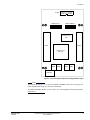
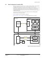
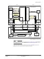
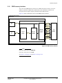
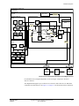
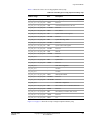
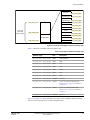
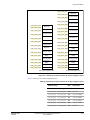
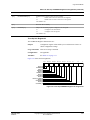
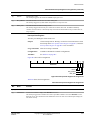
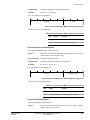
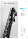
1
CoreTile Express A15×2 A7×3
™
Cortex -A15_A7 MPCore (V2P-CA15_A7)
®
™
Technical Reference Manual
Copyright © 2012-2013 ARM. All rights reserved.
ARM DDI 0503F (ID062813)
CoreTile Express A15×2 A7×3
Technical Reference Manual
Copyright © 2012-2013 ARM. All rights reserved.
Release Information
The following changes have been made to this book.
Change history
Date
Issue
Confidentiality
Change
June 2012
A
Non-Confidential
First release for V2P-CA15_A7
July 2012
B
Non-Confidential
Second release for V2P-CA15_A7
10 August 2012
C
Non-Confidential
Third release for V2P-CA15_A7
12 October 2012
D
Non-Confidential
Fourth release for V2P-CA15_A7
31 March 2013
E
Non-Confidential
Fifth release for V2P-CA15_A7
28 June 2013
F
Non-Confidential
Sixth release for V2P-CA15_A7
Proprietary Notice
Words and logos marked with ® or ™ are registered trademarks or trademarks of ARM® in the EU and other countries,
except as otherwise stated below in this proprietary notice. Other brands and names mentioned herein may be the
trademarks of their respective owners.
Neither the whole nor any part of the information contained in, or the product described in, this document may be
adapted or reproduced in any material form except with the prior written permission of the copyright holder.
The product described in this document is subject to continuous developments and improvements. All particulars of the
product and its use contained in this document are given by ARM in good faith. However, all warranties implied or
expressed, including but not limited to implied warranties of merchantability, or fitness for purpose, are excluded.
This document is intended only to assist the reader in the use of the product. ARM shall not be liable for any loss or
damage arising from the use of any information in this document, or any error or omission in such information, or any
incorrect use of the product.
Where the term ARM is used it means “ARM or any of its subsidiaries as appropriate”.
Confidentiality Status
This document is Non-Confidential. The right to use, copy and disclose this document may be subject to license
restrictions in accordance with the terms of the agreement entered into by ARM and the party that ARM delivered this
document to.
Product Status
The information in this document is final, that is for a developed product.
Web Address
http://www.arm.com
ARM DDI 0503F
ID062813
Copyright © 2012-2013 ARM. All rights reserved.
Non-Confidential
ii
Conformance Notices
This section contains conformance notices.
Federal Communications Commission Notice
This device is test equipment and consequently is exempt from part 15 of the FCC Rules under section 15.103 (c).
CE Declaration of Conformity
The system should be powered down when not in use.
The daughterboard generates, uses, and can radiate radio frequency energy and may cause harmful interference to radio
communications. However, there is no guarantee that interference will not occur in a particular installation. If this
equipment causes harmful interference to radio or television reception, which can be determined by turning the
equipment off or on, you are encouraged to try to correct the interference by one or more of the following measures:
•
Ensure attached cables do not lie across the card.
•
Reorient the receiving antenna.
•
Increase the distance between the equipment and the receiver.
•
Connect the equipment into an outlet on a circuit different from that to which the receiver is connected.
•
Consult the dealer or an experienced radio/TV technician for help.
Note
It is recommended that wherever possible shielded interface cables be used.
ARM DDI 0503F
ID062813
Copyright © 2012-2013 ARM. All rights reserved.
Non-Confidential
iii
Contents
CoreTile Express A15×2 A7×3 Technical Reference
Manual
Preface
About this book .......................................................................................................... vii
Feedback .................................................................................................................... xi
Chapter 1
Introduction
1.1
1.2
Chapter 2
Hardware Description
2.1
2.2
2.3
2.4
2.5
2.6
2.7
2.8
2.9
2.10
2.11
Chapter 3
CoreTile Express A15×2 A7×3 daughterboard architecture .................................... 2-2
Cortex-A15_A7 MPCore test chip ............................................................................ 2-4
System interconnect signals .................................................................................... 2-6
Power-up configuration and resets ........................................................................ 2-10
Serial Configuration Controller (SCC) .................................................................... 2-21
Voltage control and process monitors ................................................................... 2-22
Clocks .................................................................................................................... 2-24
Interrupts ................................................................................................................ 2-34
HDLCD .................................................................................................................. 2-38
DDR2 memory interface ........................................................................................ 2-39
Debug .................................................................................................................... 2-40
Programmers Model
3.1
3.2
3.3
3.4
ARM DDI 0503F
ID062813
About the CoreTile Express A15×2 A7×3 daughterboard ....................................... 1-2
Precautions .............................................................................................................. 1-4
About this programmers model ................................................................................ 3-2
Daughterboard memory map ................................................................................... 3-3
Test chip SCC registers ......................................................................................... 3-12
Programmable peripherals and interfaces ............................................................. 3-54
Copyright © 2012-2013 ARM. All rights reserved.
Non-Confidential
iv
Contents
Appendix A
Signal Descriptions
A.1
A.2
A.3
A.4
Appendix B
ARM DDI 0503F
ID062813
Introduction .............................................................................................................. B-2
HDLCD Programmers Model ................................................................................... B-3
Electrical Specifications
C.1
Appendix D
A-2
A-3
A-5
A-6
HDLCD controller
B.1
B.2
Appendix C
Daughterboard connectors ......................................................................................
HDRX HSB multiplexing scheme .............................................................................
Header connectors ..................................................................................................
Debug and trace connectors ....................................................................................
AC characteristics .................................................................................................... C-2
Revisions
Copyright © 2012-2013 ARM. All rights reserved.
Non-Confidential
v
Preface
This preface introduces the CoreTile Express A15×2 A7×3 Technical Reference Manual. It
contains the following sections:
•
About this book on page vii
•
Feedback on page xi.
ARM DDI 0503F
ID062813
Copyright © 2012-2013 ARM. All rights reserved.
Non-Confidential
vi
Preface
About this book
This book is for the CoreTile Express A15×2 A7×3 daughterboard.
Intended audience
This document is written for experienced hardware and software developers to aid the
development of ARM-based products using the CoreTile Express A15×2 A7×3 daughterboard
with the Motherboard Express µATX as part of a development system.
Using this book
This book is organized into the following chapters:
Chapter 1 Introduction
Read this for an introduction to the CoreTile Express A15×2 A7×3
daughterboard.
Chapter 2 Hardware Description
Read this for a description of the hardware present on the daughterboard.
Chapter 3 Programmers Model
Read this for a description of the configuration registers present on the
daughterboard.
Appendix A Signal Descriptions
Read this for a description of the signals present on the daughterboard.
Appendix B HDLCD controller
Read this for a description of the HDLCD controller in the Cortex-A15_A7 test
chip.
Appendix C Electrical Specifications
Read this for a description of the electrical specifications of the daughterboard.
Appendix D Revisions
Read this for a description of the technical changes between released issues of this
book.
Glossary
The ARM Glossary is a list of terms used in ARM documentation, together with definitions for
those terms. The ARM Glossary does not contain terms that are industry standard unless the
ARM meaning differs from the generally accepted meaning.
See ARM Glossary, http://infocenter.arm.com/help/topic/com.arm.doc.aeg0014-/index.html.
Conventions
This book uses the conventions that are described in:
•
Typographical conventions on page viii
•
Timing diagrams on page viii
•
Signals on page ix.
ARM DDI 0503F
ID062813
Copyright © 2012-2013 ARM. All rights reserved.
Non-Confidential
vii
Preface
Typographical conventions
The following table describes the typographical conventions:
Style
Purpose
italic
Introduces special terminology, denotes cross-references, and citations.
bold
Highlights interface elements, such as menu names. Denotes signal names. Also used for terms in descriptive lists,
where appropriate.
monospace
Denotes text that you can enter at the keyboard, such as commands, file and program names, and source code.
monospace
Denotes a permitted abbreviation for a command or option. You can enter the underlined text instead of the full
command or option name.
monospace italic
Denotes arguments to monospace text where the argument is to be replaced by a specific value.
monospace bold
Denotes language keywords when used outside example code.
<and>
Encloses replaceable terms for assembler syntax where they appear in code or code fragments. For example:
MRC p15, 0 <Rd>, <CRn>, <CRm>, <Opcode_2>
SMALL CAPITALS
Used in body text for a few terms that have specific technical meanings, that are defined in the ARM glossary. For
example, IMPLEMENTATION DEFINED, IMPLEMENTATION SPECIFIC, UNKNOWN, and UNPREDICTABLE.
Timing diagrams
The figure named Key to timing diagram conventions explains the components used in timing
diagrams. Variations, when they occur, have clear labels. You must not assume any timing
information that is not explicit in the diagrams.
Shaded bus and signal areas are undefined, so the bus or signal can assume any value within the
shaded area at that time. The actual level is unimportant and does not affect normal operation.
Clock
HIGH to LOW
Transient
HIGH/LOW to HIGH
Bus stable
Bus to high impedance
Bus change
High impedance to stable bus
Key to timing diagram conventions
Timing diagrams sometimes show single-bit signals as HIGH and LOW at the same time and
they look similar to the bus change shown in Key to timing diagram conventions. If a timing
diagram shows a single-bit signal in this way then its value does not affect the accompanying
description.
ARM DDI 0503F
ID062813
Copyright © 2012-2013 ARM. All rights reserved.
Non-Confidential
viii
Preface
Signals
The signal conventions are:
Signal level
The level of an asserted signal depends on whether the signal is
active-HIGH or active-LOW. Asserted means:
•
HIGH for active-HIGH signals.
•
LOW for active-LOW signals.
Lower-case n
At the start or end of a signal name denotes an active-LOW signal.
Additional reading
This section lists publications by ARM and by third parties.
See Infocenter, http://infocenter.arm.com, for access to ARM documentation.
ARM publications
This book contains information that is specific to this product. See the following documents for
other relevant information:
•
Motherboard Express µATX Technical Reference Manual (ARM DUI 0447)
•
Versatile Express™ Configuration Technical Reference Manual (ARM DDI 0496)
•
Programmer Module (V2M-CP1) (ARM DDI 0495)
•
LogicTile™ Express 3MG Technical Reference Manual (ARM DUI 0449)
•
LogicTile™ Express 13MG Technical Reference Manual (ARM DUI 0556)
•
LogicTile™ Express 20MG Technical Reference Manual (ARM DDI 0503)
•
Versatile Express™ Boot Monitor Technical Reference Manual (ARM DUI 0465)
•
Cortex® A15 Technical Reference Manual (ARM DDI 0438)
•
Cortex® A7 MPCore™ Technical Reference Manual (ARM DDI 0464)
•
AMBA® Network Interconnect (NIC-301) Technical Reference Manual (ARM DDI 0397)
•
CoreLink™ GIC-400 Generic Interrupt Controller Technical Reference Manual
(ARM DDI 0471)
•
CoreLink™ DMC-400 Dynamic Memory Controller Technical Reference Manual
(ARM DDI 0466)
•
ARM PrimeCell Static Memory Controller (PL350 series) Technical Reference Manual
(ARM DDI 0380)
•
AMBA® DMA Controller DMA-330 Technical Reference Manual (ARM DDI 0424)
•
ARM® Watchdog Module (SP805) Technical Reference Manual (ARM DDI 0270)
•
ARM® PrimeCell External Bus Interface (PL220) Technical Reference Manual
(ARM DDI 0249)
The following publications provide information about related ARM products and toolkits:
•
ARM DDI 0503F
ID062813
ARM® DSTREAM™ System and Interface Design Reference (ARM DUI 0499)
Copyright © 2012-2013 ARM. All rights reserved.
Non-Confidential
ix
Preface
ARM DDI 0503F
ID062813
•
ARM® DSTREAM™ Setting up the Hardware (ARM DUI 0481)
•
ARM® DSTREAM™and RVI™ Using the Debug Hardware Configuration Utilities
(ARM DUI 0498)
•
ARM® CoreSight™ Components Technical Reference Manual (ARM DDI 0314)
•
Application Note AN283, Example LogicTile™ Express 3MG Design for a CoreTile™
Express A15×2
•
Application Note AN305, Example LogicTile™ Express 13MG Design for a CoreTile™
Express A15×2
•
Application Note AN318, CoreTile™ Express A15×2 A7×3 Power Management.
Copyright © 2012-2013 ARM. All rights reserved.
Non-Confidential
x
Preface
Feedback
ARM welcomes feedback on this product and its documentation.
Feedback on this product
If you have any comments or suggestions about this product, contact your supplier and give:
•
The product name.
•
The product revision or version.
•
An explanation with as much information as you can provide. Include symptoms and
diagnostic procedures if appropriate.
Feedback on content
If you have comments on content then send an e-mail to [email protected]. Give:
•
the title
•
the number, ARM DDI 0503F
•
the page numbers to which your comments apply
•
a concise explanation of your comments.
ARM also welcomes general suggestions for additions and improvements.
ARM DDI 0503F
ID062813
Copyright © 2012-2013 ARM. All rights reserved.
Non-Confidential
xi
Chapter 1
Introduction
This chapter provides an introduction to the CoreTile Express A15×2 A7×3 daughterboard. It
contains the following sections:
•
About the CoreTile Express A15×2 A7×3 daughterboard on page 1-2
•
Precautions on page 1-4.
ARM DDI 0503F
ID062813
Copyright © 2012-2013 ARM. All rights reserved.
Non-Confidential
1-1
Introduction
1.1
About the CoreTile Express A15×2 A7×3 daughterboard
The CoreTile Express A15×2 A7×3 daughterboard is designed as a platform for developing
systems based on Advanced Microcontroller Bus Architecture (AMBA®) that use the Advanced
eXtensible Interface (AXI™) or custom logic for use with ARM cores.
You can use the CoreTile Express A15×2 A7×3 daughterboard to create prototype systems.
Note
You can use the CoreTile Express A15×2 A7×3 daughterboard with a Motherboard Express
µATX See System interconnect signals on page 2-6 for information about interconnection.
You can also use the CoreTile Express daughterboard with a custom-design motherboard. See
Programmer Module (V2M-CP1).
The daughterboard includes the following features:
•
Cortex-A15_A7 MPCore test chip, with NEON, the advanced Single Instruction Multiple
Data (SIMD) extension, and Floating Point Unit (FPU), that contains a dual-core A15
cluster operating at 1GHz and a triple-core A7 cluster operating at 800MHz.
•
Cortex-A15_A7 MPCore test chip internal AXI subsystem operating at 500MHz.
•
Simple configuration with V2M-P1 motherboard:
— Configuration EEPROM.
— Daughterboard Configuration Controller.
•
Nine programmable oscillators.
•
2GB of daughterboard DDR2 32-bit memory operating at 400MHz.
•
High Definition LCD (HDLCD) controller that supports up to 1920×1080p video at 60Hz,
165MHz pixel clock.
•
CoreSight software debug and 32-bit trace ports.
•
HDRX header with one multiplexed AMBA AXI master bus port that connects to the
other daughterboard site on the V2M-P1 motherboard.
•
HDRY header with four buses to the motherboard:
—
Static Memory Bus (SMB).
—
MultiMedia Bus (MMB).
—
Configuration Bus (CB).
—
System Bus (SB).
•
Power Supply Units (PSUs) for the Cortex-A15_A7 test chip and DDR2 memory.
•
Core voltage control and current, temperature, and power monitoring.
•
On-board energy meter.
Note
The Cortex-A15_A7 test chip does not support TrustZone®.
Figure 1-1 on page 1-3 shows the layout of the daughterboard:
ARM DDI 0503F
ID062813
Copyright © 2012-2013 ARM. All rights reserved.
Non-Confidential
1-2
Introduction
P-JTAG
TRACE (DUAL)
TRACE (SINGLE)
Cortex-A15_A7
PSU
HDRY
HDRX
Cortex-A15_A7
Test Chip
DDR2
DDR2
DDR2
DDR2
DDR PSU
Figure 1-1 CoreTile Express A15×2 A7×3 daughterboard layout
Note
All components in Figure 1-1, except for the HDRY and HDRX headers are on the upper face
of the daughterboard facing away from the motherboard.
The HDRX and HDRY headers are on the lower face of the daughterboard facing towards the
motherboard.
ARM DDI 0503F
ID062813
Copyright © 2012-2013 ARM. All rights reserved.
Non-Confidential
1-3
Introduction
1.2
Precautions
This section contains advice about how to prevent damage to your daughterboard.
1.2.1
Ensuring safety
The daughterboard is supplied with a range of DC voltages. Power is supplied to the
daughterboard through the header connectors.
Warning
Do not use the board near equipment that is sensitive to electromagnetic emissions, for example
medical equipment.
1.2.2
Preventing damage
The daughterboard is intended for use within a laboratory or engineering development
environment. It is supplied without an enclosure and this leaves the board sensitive to
electrostatic discharges and permits electromagnetic emissions.
Caution
To avoid damage to the daughterboard, observe the following precautions:
ARM DDI 0503F
ID062813
•
Never subject the board to high electrostatic potentials. Observe ElectroStatic Discharge
(ESD) precautions when handling any board.
•
Always wear a grounding strap when handling the board.
•
Only hold the board by the edges.
•
Avoid touching the component pins or any other metallic element.
•
Do not use the board near a transmitter of electromagnetic emissions.
Copyright © 2012-2013 ARM. All rights reserved.
Non-Confidential
1-4
Chapter 2
Hardware Description
This chapter describes the hardware on the CoreTile Express A15×2 A7×3 daughterboard. It
contains the following sections:
•
CoreTile Express A15×2 A7×3 daughterboard architecture on page 2-2
•
Cortex-A15_A7 MPCore test chip on page 2-4
•
System interconnect signals on page 2-6
•
Power-up configuration and resets on page 2-10
•
Serial Configuration Controller (SCC) on page 2-21
•
Voltage control and process monitors on page 2-22
•
Clocks on page 2-24
•
Interrupts on page 2-34
•
HDLCD on page 2-38.
•
DDR2 memory interface on page 2-39
•
Debug on page 2-40.
ARM DDI 0503F
ID062813
Copyright © 2012-2013 ARM. All rights reserved.
Non-Confidential
2-1
Hardware Description
2.1
CoreTile Express A15×2 A7×3 daughterboard architecture
Figure 2-1 shows a block diagram of the daughterboard.
CoreTile Express A15x2 A7x3
Daughterboard
P-JTAG/SWD
Trace Dual
(32-bit trace)
JTAG/SWD
(DAP/TAP)
Clock
generator
logic
Trace Single
(16-bit trace)
32-bit trace
DDR2 2GB
(32-bit)
DDR2
Serial
configuration
Interrupts
Cortex-A15_A7
Test Chip
Daughterboard
Configuration
Controller
Static
Memory Bus
AXI master
Configuration
EEPROM
HDLCD
SB
HSB (M)
CB
SMB
MMB
HDRY
HDRX
Figure 2-1 CoreTile Express A15×2 A7×3 daughterboard block diagram
The daughterboard contains the following devices and interfaces:
Cortex-A15_A7 MPCore test chip
Dual-core A15 cluster, version r2p1, operating at 1GHz.
Triple-core A7 cluster, version r0p1, operating at 800MHz.
Daughterboard Configuration Controller
The Daughterboard Configuration Controller communicates with the
Motherboard Configuration Controller (MCC) on the Motherboard Express
μATX. The Daughterboard Configuration Controller and MCC initiate, control,
and configure the test chip and the daughterboard.
Configuration EEPROM
The daughterboard EEPROM contains configuration information for
identification and detection of the daughterboard during power-up and reset.
High-Definition LCD (HDLCD)
HDLCD interface to the Motherboard Express through the MultiMedia Bus
(MMB).
DDR2 memory
The daughterboard supports 2GB of 32-bit DDR2 on-board memory.
ARM DDI 0503F
ID062813
Copyright © 2012-2013 ARM. All rights reserved.
Non-Confidential
2-2
Hardware Description
Clock generators
The daughterboard provides nine on-board OSCCLKS to drive the core and
internal AXI, AXIM, DDR2, SMC, and HDLCD interfaces.
CoreSight software debug (P-JTAG) and trace ports
The Cortex-A15_A7 MPCore test chip CoreSight system supports both the SWD
and P_JTAG protocols.
A 32-bit trace interface is provided through the standard dual 16-bit Matched
Impedance ConnecTOR (MICTOR) connectors.
System interconnect
HDRX header
Connects the multiplexed AXI master bus, HSB M, to the
external AXI slave on the other daughterboard in Site 2 of
the V2M-P1 Motherboard Express.
HDRY header
Connects the Configuration Bus (CB), the System Bus (SB),
the Static Memory Bus (SMB) and the MultiMedia Bus
(MMB) to the V2M-P1 Motherboard Express.
Note
ARM recommends that you fit the CoreTile Express A15×2 A7×3 daughterboard
on Motherboard Express site 1, and any optional FPGA daughterboard, for
example the V2F_1XV5, on site 2.
See System interconnect signals on page 2-6.
ARM DDI 0503F
ID062813
Copyright © 2012-2013 ARM. All rights reserved.
Non-Confidential
2-3
Hardware Description
2.2
Cortex-A15_A7 MPCore test chip
Figure 2-2 shows the main components of the test chip.
P-JTAG/SWD
CoreTile Express A15x2 A7x3 Daughterboard
Cortex-A15_A7
Test Chip
Trace
DAP, TPIU and CTI
GIC-400
Interrupt controller
Async
Cortex-A15
MPCore Cluster
Cortex-A15
Cortex-A15 Cortex-A15
MPCore
CORE0
CORE1
Cortex-A7
MPCore Cluster
Cortex-A7
Cortex-A7
MPCore
CORE0
Async
Cortex-A7
CORE1
Cortex-A7
CORE2
Snoop Control Unit
M
Snoop Control Unit
M
Cache controller
and 1MB L2 RAM
Cache controller
and 512KB L2 RAM
ACP (SO)
ACE
ACE
Async
Async
Async
Funnel
128-bit
128-bit
PL330 DMA
controller
S1
CCI-400 Cache Coherent Interconnect
S2
S3
Reset logic
M1 M2
Test chip SCC
S4
M0
128-bit
128-bit
128-bit
AXI to APB
S
NIC-301 AXI interconnect
M
M
M
M
64-bit
Internal clock
generation (PLLs)
64-bit
DMC-400
HDLCD
DDR2
PHY
24-bit
RGB
32-bit
DDR2
CB
SB
PL354
Dual SMC
64KB
System
SRAM
64-bit
PL220
interface
Multiplexer
SMB
AXI M
Clock generator
Daughterboard
Configuration
Controller
MMB
DDR2
HDRY
HDRX
Figure 2-2 Top-level view of the Cortex-A15_A7 MPCore test chip components
ARM DDI 0503F
ID062813
Copyright © 2012-2013 ARM. All rights reserved.
Non-Confidential
2-4
Hardware Description
Note
Bus lines with single-headed arrows indicate the direction of control, not the direction of data
flow. That is, each arrow points from bus master to bus slave.
Cortex-A15_A7 MPCore test chip
The test chip includes the following components and interfaces:
•
Cortex-A15 dual-core cluster operating at 1GHz:
— Version r2p1.
— 32KB I/D cache.
— NEON and Floating Point Unit (FPU).
— ACP port.
— 1MB L2 cache.
— Dual Program Flow Trace Macrocell (PTM).
•
Cortex-A7 triple-core cluster operating at 800MHz:
— Version r0p1.
— 32KB I/D cache.
— NEON and FPU.
— 512KB L2 cache.
— Dual Embedded Trace Macrocell (ETM).
•
NIC-301 AXI interconnect operating at 500MHz.
•
CCI-400 cache coherent interconnect operating at 500MHz that provides
cache-coherency between the two clusters.
•
DMC-400 32-bit Double Data Rate 2 (DDR2) Dynamic Memory
Controller (DMC) interface to the onboard 2GB DDR2 memory.
•
PL354 32-bit SMB controller (SMC). This connects to the motherboard
peripherals.
•
PL330 Direct Memory Access (DMA) controller.
•
24-bit HDLCD video controller that drives the MMB to the MUXFPGA on
the V2M-P1 Motherboard Express.
•
Multiplexed 64-bit AXI master interface.
•
64KB of local on-chip SRAM.
•
CoreSight debug and trace interface to the onboard connectors:
•
•
—
PTM for each Cortex-A15 core.
—
ETM for each Cortex-A7 core.
—
16KB ETB.
—
DAP.
—
Trace Port Interface Unit (TPIU) for real-time trace data.
—
JTAG interface for debug.
Serial Configuration Controller (SCC) interface:
—
Interfaces to the Daughterboard Configuration Controller.
—
Configures the test chip Phase-Locked Loops (PLLs) during power
up or reset.
Interrupts interface:
—
ARM DDI 0503F
ID062813
Connects interrupt signals from the V2M-P1 motherboard to the
Generic Interrupt Controller (GIC) in the test chip.
Copyright © 2012-2013 ARM. All rights reserved.
Non-Confidential
2-5
Hardware Description
2.3
System interconnect signals
This section provides an overview of the signals present on the header connectors. It contains
the following sections:
•
Overview of system interconnect signals
•
High-Speed Bus (HSB) to other daughterboard on page 2-8
•
Static Memory Bus (SMB) on page 2-8
•
MultiMedia Bus (MMB) on page 2-8
•
System Bus (SB) on page 2-9
•
Configuration Bus (CB) on page 2-9.
2.3.1
Overview of system interconnect signals
Figure 2-3 on page 2-7 shows the daughterboard system interconnect to the Motherboard
Express µATX development system and to an optional LogicTile™ Express FPGA
daughterboard. For more information about the global interconnect scheme, see the
Motherboard Express µATX Technical Reference Manual.
ARM DDI 0503F
ID062813
Copyright © 2012-2013 ARM. All rights reserved.
Non-Confidential
2-6
Hardware Description
Site 1
Site 2
CoreTile Express
A15x2 A7x3 Daughterboard
Daughterboard
Configuration
Controller
LogicTile Express
FPGA
Daughterboard
DDR2
memory
Cortex-A15_A7
Test Chip
HDRY
HDRX
HDRX
HDRY
SMB2
SB1
SMB1
CB
Daughterboard
Configuration
Controller
FPGA
HSB (M)
HSB (M)
HDRX1
PCIe2
CB
MMB2
HSB (S)
MMB1
HDRY1
SB2
HDRX2
HDRY2
PCIe2
SMB1
SB
Motherboard I/O FPGA
Motherboard
Configuration
Controller
(MCC)
SMB2
MMB1
MMB2
Multiplexer
FPGA
PCIe1
PCIe
Switch
Configuration
flash memory
(USBMSD)
Motherboard Express μATX
V2M-P1
USB
DVI
PCIe
Slots
Figure 2-3 System connect example with optional LogicTile Express FPGA daughterboard
•
ARM DDI 0503F
ID062813
Note
ARM recommends that you fit CoreTile Express daughterboards, including the CoreTile
Express A15×2 A7×3 daughterboard, on site 1, and that you fit LogicTile Express FPGA
daughterboards on site 2.
•
The CoreTile Express A15×2 A7×3 daughterboard does not have an High-Speed Bus
(HSB) slave port or a PCI express root complex.
•
Application note AN283, Example LogicTile™ Express 3MG design for a CoreTile™
Express A15×2, that ARM provides, implements an example AMBA system using the
LogicTile Express V2F-1XV5 daughterboard to interconnect with the CoreTile
Copyright © 2012-2013 ARM. All rights reserved.
Non-Confidential
2-7
Hardware Description
Express A15×2 A7×3 daughterboard. See the documentation supplied on the
accompanying media and the Application Notes listing for more information at,
http://infocenter.arm.com.
2.3.2
High-Speed Bus (HSB) to other daughterboard
The HSB link to the other daughterboard consists of one bus between the Cortex-A15_A7
MPCore test chip and the daughterboard fitted in the other site on the motherboard. This is a
64-bit multiplexed AXI master bus, HSB M, to the external AXI slave on the other
daughterboard in Site 2.
The HSB connection to the other daughterboard is through:
•
The HDRX header on the daughterboard.
•
Dedicated headers HDRX1 and HDRX2 on the motherboard.
•
Header HDRX on the other daughterboard.
Note
For information about the multiplexing scheme for the AXI buses, see Appendix A Signal
Descriptions.
Note
Application note AN283, Example LogicTile™ Express 3MG design for a CoreTile™ Express
A15×2, provides an example AXI design implementing an external multiplexed AXI master bus
at the HDRX header on the FPGA daughterboard in site 2.
2.3.3
Static Memory Bus (SMB)
The SMB connects the Cortex-A15_A7 test chip SMC to the motherboard. You can use it to
access the motherboard peripherals such as:
•
NOR flash.
•
SRAM.
•
Ethernet.
•
USB.
•
MultiMedia Card (MMC).
•
Compact Flash (CF).
•
Keyboard and Mouse Interface (KMI).
•
CLCD.
•
UARTs.
•
System registers.
2.3.4
MultiMedia Bus (MMB)
The MMB consists of a video bus that connects the 24-bit RGB HDLCD controller directly to
the motherboard MUXFPGA. The motherboard IOFPGA implements a CLCD controller. The
motherboard MUXFPGA selects the source for the motherboard DVI connector from:
ARM DDI 0503F
ID062813
•
The MMB from the CoreTile Express A15×2 A7×3. That is, the 24-bit RGB from the
HDLCD controller.
•
The MMB from the LogicTile Express daughterboard in site 2.
•
The CLCD controller in the motherboard IOFPGA.
Copyright © 2012-2013 ARM. All rights reserved.
Non-Confidential
2-8
Hardware Description
2.3.5
System Bus (SB)
The SB connects 26 interrupt lines from motherboard peripherals to the Generic Interrupt
Controller (GIC) in the MPCore cluster in the test chip.
2.3.6
Configuration Bus (CB)
The CB connects the Daughterboard Configuration Controller to the MCC. The Daughterboard
Configuration Controller configures the OSCCLKs on the daughterboard and the
Cortex-A15_A7 test chip SCC registers. The Daughterboard Configuration Controller also
controls daughterboard resets and temperature monitoring. The CB connects the daughterboard
EEPROM directly to the MCC and enables automatic detection and identification of the
daughterboard at power-up or reset.
ARM DDI 0503F
ID062813
Copyright © 2012-2013 ARM. All rights reserved.
Non-Confidential
2-9
Hardware Description
2.4
Power-up configuration and resets
This section describes the CoreTile Express A15×2 daughterboard power-up configuration and
resets. It contains the following subsections:
•
Configuration architecture
•
System configuration on page 2-13
•
Resets on page 2-13
•
Configuration and reset signals on page 2-13.
2.4.1
Configuration architecture
Figure 2-4 shows the power-up, configuration, and reset architecture when the CoreTile Express
A15×2 daughterboard is fitted to a Motherboard Express, V2M-P1.
CoreTile Express
A15x2 A7x3 Daughterboard
Clock
generator
logic
PLLs
Cortex-A15_A7
Test Chip
SCC
Configuration
EEPROM
Daughterboard
Configuration
Controller
HDRY
CB
HDRY1
CB
UART0 DSR and CTS
Configuration
EEPROM
MCC UART
MCC UART
ON/OFF/Soft
Reset
Hardware RESET
DCC1 UART
MCC
IO FPGA
Power-on detect
microSD
card
(USBMSD)
DCC2 UART
USB-B
port
UART0 Port
UART1 Port
UART2 Port
UART3 Port
NOR
flash
Motherboard Express (V2M-P1)
Figure 2-4 CoreTile Express A15×2 A7×3 configuration architecture with Motherboard Express, V2M-P1
Note
ARM recommends that you fit the CoreTile Express A15×2 A7×3 daughterboard in site 1.
ARM DDI 0503F
ID062813
Copyright © 2012-2013 ARM. All rights reserved.
Non-Confidential
2-10
Hardware Description
The configuration environment of the CoreTile Express A15×2 A7×3 daughterboard fitted to
the Motherboard Express, V2M-P1, consists of the following hardware components:
•
MCC on the Motherboard Express, V2M-P1.
•
Daughterboard Configuration Controllers on the CoreTile Express daughterboard and on
the LogicTile Express daughterboard.
•
Configuration microSD card or Universal Serial Bus Mass Storage Device (USBMSD)
on the Motherboard Express, V2M-P1.
•
Configuration EEPROM on the Motherboard Express, V2M-P1.
•
Clock generator logic on the V2P-CA15_A7 daughterboard.
•
ON/OFF/Soft Reset and Hardware RESET buttons on the Motherboard Express,
V2M-P1.
•
USB-B port on the Motherboard Express, V2M-P1.
•
Four UART ports on the Motherboard Express, V2M-P1.
•
NOR flash on the Motherboard Express, V2M-P1.
•
Power-on detect on the Motherboard Express, V2M-P1.
•
Configuration EEPROM on the V2P-CA15 daughterboard.
•
HDRY headers on the Motherboard Express, V2M-P1, and V2P-CA15_A7
daughterboard.
Figure 2-5 on page 2-12 shows the power-up, configuration, and reset architecture when the
CoreTile Express A15×2 A7×3 daughterboard is fitted to a V2M-CP1 Programmer Module, and
custom motherboard built under the ARM Design Assist Program.
ARM DDI 0503F
ID062813
Copyright © 2012-2013 ARM. All rights reserved.
Non-Confidential
2-11
Hardware Description
Programmer Module
V2M-CP1
Ethernet
USB
UART
CoreTile Express
A15x2 A7X3 Daughterboard
Clock
generator
logic
PLLs
Cortex-A15_A7
Test Chip
SCC
SD card
(USBMSD)
Daughterboard
Configuration
Controller
MCC
ON/OFF/Soft
Reset
Configuration
EEPROM
Hardware RESET
PROGRAM HEADER
HDRY
PROGRAM HEADER
HDRY
SSP_ADDR
EEPROM
SPI
CB
Control
SPI
V2M-DA1 Motherboard
PCM
Flash
Figure 2-5 CoreTile Express A15×2 A7×3 configuration architecture with custom motherboard
The configuration environment of a V2P-CA15_A7 daughterboard fitted to a custom
motherboard and a V2M-CP1 Programmer Module consists of:
•
MCC on the V2M-CP1.
•
Daughterboard Configuration Controller on the V2P-CA15 daughterboard.
•
Configuration microSD card or USBMSD on the V2M-CP1 Programmer Module.
•
ON/OFF/soft reset and hardware reset buttons on the V2M-CP1 Programmer Module.
•
USB port on the V2M-CP1 Programmer Module.
•
Ethernet port on the V2M-CP1 Programmer Module.
Note
The V2M-CP1 Programmer Module does not support the ethernet port.
ARM DDI 0503F
ID062813
•
Configuration EEPROM on the custom motherboard.
•
Configuration EEPROM on V2P-CA15_A7 daughterboard.
•
Clock generator logic on the V2P-CA15_A7 daughterboard.
Copyright © 2012-2013 ARM. All rights reserved.
Non-Confidential
2-12
Hardware Description
2.4.2
System configuration
See the Versatile Express™ Configuration Technical Reference Manual and Motherboard
Express (μATX) or Programmer Module (V2M-CP1) for information on how to configure the
V2P-CA15_A7 daughterboard using the configuration files on the motherboard.
Caution
ARM recommends that you use the configuration files for all system configuration. Test chip
SCC registers on page 3-12 and Programmable peripherals and interfaces on page 3-54
describe registers that directly modify the test chip configuration.
2.4.3
Resets
The Daughterboard Configuration Controller manages reset signals between the motherboard
and the daughterboard test chip in response to reset requests from the motherboard MCC as a
result of, for example, pressing the motherboard power/reset push-button.
2.4.4
Configuration and reset signals
This section describes the configuration and reset signals and their sequences and timings. It
contains the following sections:
•
Overview of daughterboard reset signals
•
Configuration and reset timing cycle on page 2-14
•
Configuration and reset signals on page 2-15
•
Internal resets on page 2-17.
Overview of daughterboard reset signals
Figure 2-6 on page 2-14 shows an overview of the daughterboard reset signals and includes
configuration signals.
ARM DDI 0503F
ID062813
Copyright © 2012-2013 ARM. All rights reserved.
Non-Confidential
2-13
Hardware Description
CoreTile Express A15x2 A7x3
Daughterboard
OSCCLKS
1
CB_CFGnRST
2
nCFGRST
Cortex-A15_A7
Test Chip
CB_OK
3
SCC
Registers
CB_SSPx
4
Daughterboard
Configuration
Controller
CB_READY
6
nPLLRST
PLLS_LOCKED
CB_nPOR
nPORESET
CB_nRST
nRESET
7
8
CB_RSTREQ
nSRST
nTRST
nTRST
JTAG
HDRY
HDRY1
5
MBM_nRST
MBM_nRST
IOPFGA
Motherboard Configuration
Controller (MCC)
nPOR
Motherboard Express μATX
V2M-P1
Figure 2-6 CoreTile Express A15×2 A7×3 daughterboard resets
Note
The numbers in Figure 2-6 represent stages in the reset and configuration process. See
Figure 2-7 on page 2-15.
Configuration and reset timing cycle
Figure 2-7 on page 2-15 shows the CoreTile Express A15×2 daughterboard power-up
configuration and reset timing cycle.
ARM DDI 0503F
ID062813
Copyright © 2012-2013 ARM. All rights reserved.
Non-Confidential
2-14
Hardware Description
1
2
3
4
5
SPI
DB
IOFPGA
Daughterboard
configure configure
ready
Configuration Controller
d
d
reset
ready
CB_CFGnRS
T
6
Cold
reset
7
Warm
reset
8
Run
9
10
ICE or Cold/Warm
Soft reset reset
1
1
Run
CB_OK
CB_READY
IOFPGA
MBM_nRST
CB_nPO
R
CB_nRST
CB_RSTRE
Q
On/Off/Soft
reset button
Either a soft reset from
motherboard or a reset
request from
daughterboard
Figure 2-7 CoreTile Express A15×2 A7×3 daughterboard configuration and reset timing cycle
Configuration and reset signals
Table 2-1 shows the Cortex-A15_A7 MPCore test chip configuration and reset signals:
Table 2-1 Configuration and reset signals
Reset source
Destination
Description
CB_CFGnRST
Daughterboard
Configuration
Controller
Initiate the daughterboard configuration process.
CB_OK
MCC
Daughterboard configuration system ready.
CB_SSPxa
Daughterboard
Configuration
Controller-MCC
Signal transactions during time period 3, DB configuration, that cause the
Daughterboard Configuration Controller to configure the Cortex-A15 MPCore
test chip SCC registers and daughterboard OSCCLKs.
CB_READY
MCC
Daughterboard configured and ready.
The PLLS_LOCKEDa signal and the control signalsa between the Daughterboard
Configuration Controller, Cortex-A15 MPCore test chip, and the daughterboard
OSCLCLKS indicate to the Daughterboard Configuration Controller and MCC
that the PLLs are locked and that the daughterboard OSCCLKS are operating.
CB_nPOR
ARM DDI 0503F
ID062813
Test chip internal
signal nPORESET
This is the main power-on-reset that resets the entire test chip logic and the clock
generation logic except for the PLLs.
Copyright © 2012-2013 ARM. All rights reserved.
Non-Confidential
2-15
Hardware Description
Table 2-1 Configuration and reset signals (continued)
Reset source
Destination
Description
CB_nRST
Test chip internal
signal nRESET
This is a hard reset from the motherboard that resets boths cores in the Cortex-A15
dual-core cluster and all three cores in the Cortex-A7 triple-core cluster.
The following internal resets, that the SCC reset control register controls, enable
reset of specific sections of the test chip. The multi-signal resets, for example
A15_nCPURESET[1:0], enable reset of specific cores or ETMs, according to the
bits selected in the SCC reset control register.
These internal resets operate independently of nRESET:
•
A15_nCPURESET[1:0]
Note
The Cortex®-A15 Technical Reference Manual names this signal as
nCPUPORESET.
•
A7_nCPURESET[2:0]
Note
The Cortex®-A7 MPCore™ Technical Reference Manual names this signal as
nCOREPORESET.
•
A15_nCORERESET[1:0].
•
A7_nCORERESET[2:0].
•
A15_nCXRESET[1:0].
•
A15_nDBGRESET[1:0].
•
A7_nDBGRESET[2:0].
•
A7_nETMRESET[2:0].
•
A15_nPRESETDBG.
•
A7_nSOCDBGRESET.
•
A15_nL2RESET.
•
A7_nL2RESET.
•
A7_nVSOCRESET.
•
A7_nVCORERESET.
•
A15_nVSOCRESET.
•
A15_nVCORERESET.
See Internal resets on page 2-17.
See the reset control register, Test chip SCC Register 6 on page 3-22, for information
on controlling these internal resets.
See the Cortex®-A15 Technical Reference Manual and the Cortex®-A7 MPCore™
Technical Reference Manual for information on using the above internal resets.
JTAG nTRSTa
Test chip internal
signal nTRST
This is the test logic reset to the Cortex-A15 MPCore test chip TAP controller and
the Daughterboard Configuration Controller.
JTAG nSRSTa
CB_RSTREQ to
motherboard MCC
If an external source asserts the JTAG nSRST signal, the daughterboard generates a
reset request to the motherboard MCC. The motherboard hardware is reset and the
MCC asserts CB_nRST, and optionally, CB_nPORb.
nSRST remains LOW until the reset sequence completes.
CB_RSTREQb
MCC
Reset request from the daughterboard to the motherboard.
Test chip watchdogs
Test chip internal
nPORESET
If the internal test chip watchdog timers are configured and trigger, they force an
internal test chip nPORESET.
The external system components on the motherboard are not reset.
a. Figure 2-7 on page 2-15 does not include these signals.
ARM DDI 0503F
ID062813
Copyright © 2012-2013 ARM. All rights reserved.
Non-Confidential
2-16
Hardware Description
b. The reset request from the daughterboard results in the motherboard asserting CB_nRST.
CB_nPOR can optionally be asserted by correctly defining the value of ASSERTNPOR, that can be TRUE or FALSE in the config.txt
motherboard configuration file. See the Motherboard Express μATX Technical Reference Manual for an example config.txt file.
Internal resets
Test chip SCC Register 6 on page 3-22 controls the internal resets that operate independently of
nRESET. Table 2-2 shows the blocks that the internal resets control.
Table 2-2 Internal resets controlled by SCC registers
Shared
debug,
APB, CTI
and CTM
logic
Shared L2
memory
system,
GIC and
timer
logic
Reset
Core
NEON
and
VFP
Debug
PTM
ETM
Breakpoint
and
watchpoint
logic
A15_NCPURESET
Yes
Yes
Yes
Yes
Yes
No
No
A15_CLK
domain.
Fine-grain
reset.
A7_NCPURESET
Yes
Yes
Yes
Yes
Yes
No
No
A7_CLK
domain.
Fine-grain
reset.
A15_NCORERESET
Yes
Yes
No
No
No
No
No
A15_CLK
domain.
Fine-grain
reset.
A7_NCORERESET
Yes
Yes
No
No
No
No
No
A7_CLK
domain.
Fine-grain
reset.
A15_NCXRESET
No
Yes
No
No
No
No
No
A15_CLK
domain.
Fine-grain
reset.
A15_NDBGRESET
No
No
Yes
Yes
Yes
No
No
A15_CLK
domain.
Fine-grain
reset.
A7_NDBGRESET
No
No
Yes
Yes
Yes
No
No
A7_NETMRESET
No
No
No
Yes
Yes
No
No
A7_CLK
domain.
Fine-grain
reset.
A15_NPRESETDBG
No
No
No
No
N
Yes
No
ARM DDI 0503F
ID062813
Copyright © 2012-2013 ARM. All rights reserved.
Non-Confidential
Comment
A15_CLK
domain.
Overrides
fine-grain
resets.
2-17
Hardware Description
Table 2-2 Internal resets controlled by SCC registers (continued)
Shared
debug,
APB, CTI
and CTM
logic
Shared L2
memory
system,
GIC and
timer
logic
Reset
Core
NEON
and
VFP
Debug
PTM
ETM
Breakpoint
and
watchpoint
logic
A7_NSOCDBGRESET
No
No
Yes
Yes
Yes
Yes
No
A7_CLK
domain.
Overrides
fine-grain
resets.
A15_NL2RESET
No
No
No
No
No
No
Yes
A15_CLK
domain.
Overrides
fine-grain
resets.
A7_NL2RESET
No
No
No
No
No
No
Yes
A7_CLK
domain.
Overrides
fine-grain
resets.
A7_NVSOCRESET
No
No
No
No
No
No
No
ACLK and
PCLK
domain.
Overrides
fine-grain
resets.
ARM DDI 0503F
ID062813
Copyright © 2012-2013 ARM. All rights reserved.
Non-Confidential
Comment
2-18
Hardware Description
Table 2-2 Internal resets controlled by SCC registers (continued)
Shared
debug,
APB, CTI
and CTM
logic
Shared L2
memory
system,
GIC and
timer
logic
Reset
Core
NEON
and
VFP
Debug
PTM
ETM
Breakpoint
and
watchpoint
logic
A7_NVCORERESET
-
Yes
Yes
Yes
Yes
Yes
Yes
A7_CLK
domain.
Overrides
fine-grain
resets.
This reset
selects all
cores in the
cluster. It
does not
select
specific
cores.
A15_NVSOCRESET
No
No
No
No
No
No
No
ACLK and
PCLK
domain.
A15_NVCORERESET
-
Yes
Yes
Yes
Yes
Yes
Yes
A15_CLK
domain.
Overrides
fine-grain
resets.
This reset
selects all
cores in the
cluster. It
does not
select
specific
cores.
Comment
Test chip SCC Register 6 on page 3-22 controls the internal resets. The fine-grained resets select
specific cores or other blocks according to the bits you select in this register.
Each cluster contains the following power domains:
VCORE
Contains most of the cluster logic including all the cores.
VSOC
Contains the interface logic between the clusters and the rest of the test chip.
The reset signals operate as follows:
A7_NVCORERESET
Resets all of the A7 VCORE domain and overrides all the fine-grained A7 resets.
A15_NVCORERESET
Resets all of the A15 VCORE domain and overrides all the fine-grained A15
resets.
ARM DDI 0503F
ID062813
Copyright © 2012-2013 ARM. All rights reserved.
Non-Confidential
2-19
Hardware Description
A7_NVSOCRESET
Resets the interface logic between the A7 VCORE and VSOC domains.
A15_NVSOCRESET
Resets the interface logic between the A15 VCORE and VSOC domains.
See the following for more information on the internal resets:
•
Cortex®-A7 MPCore™ Technical Reference Manual
•
Cortex®-A15 Technical Reference Manual.
Note
When power-management is enabled in the board.txt file, the CA15 or CA7 cores must not
directly write to CFGREG6 or CFGREG11 because the Daughterboard Configuration
Controller controls this. Writing to these registers prevents the power-management interface
from functioning correctly.
ARM DDI 0503F
ID062813
Copyright © 2012-2013 ARM. All rights reserved.
Non-Confidential
2-20
Hardware Description
2.5
Serial Configuration Controller (SCC)
The Serial Configuration Controller (SCC) is a block of registers internal to the test chip that
the Daughterboard Configuration Controller writes through a serial interface. The
Daughterboard Configuration Controller uses the SCC during power-up configuration to set the
test chip PLLs and other default values from the board configuration files stored on the
motherboard microSD card. The MCC also uses the SCC to read values from the test chip, for
example, the device ID.
You can also read and write to the SCC registers while the system is running using the
motherboard SYS_CFG register interface.
Figure 2-8 shows an overview of the SCC connectivity.
See Test chip SCC registers on page 3-12 for a full description of the SCC registers.
CoreTile Express A15x2 A7x3
Daughterboard
Cortex-A15_A7
Test Chip
Cortex-A15
MPCore
Cluster
Daughterboard
Configuration
Controller
Cortex-A7
MPCore
Cluster
SCC
registers
SCC configuration
CCI-400 interconnect
CCI-400 interconnect
HDRY
CB(SPI)
SMB
HDRY1
IOFPGA
Internal Static
Memory Bus
Matrix
Interrupt
SYS_CFG
registers
MCC
USBMSD
Motherboard Express μATX
V2M-P1
Figure 2-8 Overview of SCC connectivity
ARM DDI 0503F
ID062813
Copyright © 2012-2013 ARM. All rights reserved.
Non-Confidential
2-21
Hardware Description
2.6
Voltage control and process monitors
This section describes the V2P_CA15_A7 daughterboard core voltage control and current,
temperature, power, and energy monitoring. It contains the following subsections:
•
Voltage control and current, temperature, and power monitoring
•
Energy meter on page 2-23.
See application note AN318, CoreTile™ Express A15×2 A7×3 Power Management for more
information.
2.6.1
Voltage control and current, temperature, and power monitoring
The Daughterboard Configuration Controller transmits voltage and current measurements for
the Cortex-A15 and Cortex-A7 clusters to the motherboard where they can be read from the
SYS_CFG register interface.
Table 2-3 shows the device numbers for monitoring and setting the cluster voltages.
Table 2-3 Monitoring and setting the cluster voltages
Device
Cluster voltage supply
Default voltage
Description
0
Vcore
0.9V +/-2%
Sets and reads Cortex-A15 core voltage
1
Vcore
0.9V +/-2%
Sets and reads Cortex-A7 core voltage
Table 2-4 shows the device numbers for monitoring the current in the cluster.
Table 2-4 Cluster current monitors
Device
Cluster current
Description
0
Icore
Current measurement device for the two Cortex-A15 cores, total current
1
Icore
Current measurement device for the three Cortex-A7 cores, total current
Table 2-5 shows the device number for monitoring the power in the cluster.
Table 2-5 Cluster power monitors
Device
Cluster power
Description
0
Pcore
Power measurement device for the two Cortex-A15 cores, total power
1
Pcore
Power measurement device for the three Cortex-A7 cores, total power
Table 2-6 shows the device number for monitoring the Daughterboard Configuration Controller
temperature.
Table 2-6 Device number for monitoring the Daughterboard Configuration Controller
temperature
ARM DDI 0503F
ID062813
Device
Description
0
Measurement device for the Daughterboard Configuration Controller internal
operating temperature
Copyright © 2012-2013 ARM. All rights reserved.
Non-Confidential
2-22
Hardware Description
2.6.2
Energy meter
The Daughterboard Configuration Controller firmware supports an on-board energy meter that
enables you to measure the energy consumption of core supplies. The energy meter runs as a
background task on the Daughterboard Configuration Controller and does not load the main
core software except when you request a reading through the SYS_CFG interface.
You can use the energy meter to determine the amount of energy that a specific software
function consumes. You read the energy before and after the function operates, and the
difference between the two represents the amount of energy that the function consumes.
The energy meter accumulates core power supply at a rate of 10000 samples per second. You
can read accumulated energy since reset in Micro-Joules through the SYS_CFGCTRL register
interface.
A 64-bit value represents the total energy. This requires two 32-bit reads from the SYS_CFG
interface. You must read the lower 32 bits followed by the upper 32 bits. When you read the
lower 32 bits, the 64-bit data transfers to two temporary storage registers in the Daughterboard
Configuration Controller and you then receive the lower 32 bits from the lower storage register.
You then read the upper 32 bits and receive the value from the upper storage register.
If you read the upper 32 bits first, no data transfers to the storage register and you receive a false
energy reading.
The energy value is the energy since reset. You can also clear the energy value by writing
0x0000_0000 to the lower 32 bits.
Table 2-7 shows the device numbers for monitoring the cluster energy consumption.
Table 2-7 Cluster energy monitors
Device
Cluster energy
Description
0
Jcore
Energy meter for the two A15 cores, lower 32 bits, total energy
1
Jcore
Energy meter for the two A15 cores, upper 32 bits, total energy
2
Jcore
Energy meter for the three A7 cores, lower 32 bits, total energy
3
Jcore
Energy meter for the three A7 cores, upper 32 bits, total energy
See the Motherboard Express µATX Technical Reference Manual for more information on the
SYS_CFGCTRL registers.
ARM DDI 0503F
ID062813
Copyright © 2012-2013 ARM. All rights reserved.
Non-Confidential
2-23
Hardware Description
2.7
Clocks
This section describes the daughterboard clocks. It contains the following subsections.
•
Overview of clocks
•
Daughterboard programmable clock generators on page 2-27
•
Test chip PLLs and clock divider logic on page 2-30
•
External clocks on page 2-32.
2.7.1
Overview of clocks
The daughterboard sends clocks to, and receives clocks from, the motherboard and generates
local clocks that are imported into the Cortex-A15_A7 MPCore test chip. Additional PLLs
inside the test chip provide phase-shifted and frequency-multiplied versions of these imported
clocks as Figure 2-10 on page 2-26 shows.
Figure 2-9 on page 2-25 shows a functional overview of the CoreTile Express A15×2 A7×3
daughterboard clocks and their connections to the motherboard and a LogicTile Express FPGA
daughterboard.
ARM DDI 0503F
ID062813
Copyright © 2012-2013 ARM. All rights reserved.
Non-Confidential
2-24
Hardware Description
Site 1
CoreTile Express A15x2 A7X3
Daughterboard
DDR2
SDRAM
Site 2
LogicTile Express
FPGA Daughterboard
Cortex-A15_A7
Test Chip
DDR clocks
OSCCLKS
SMBREFCLK
DDRREFCLK
CPUREFCLK0_A7
CPUREFCLK1_A7
CPUREFCLK0_A15
CPUREFCLK1_A15
SYSREFCLK
PXLREFCLK
FPGA ref clocks
FPGA
PCI ref clock
MMB clocks
MMB_IDCLK
SMB_CLKO
SMB_CLKI
Daughterboard
Configuration
Controller
SMB_CLKO
SMB feedback
Daughterboard
Configuration
Controller
HSBM (CLK)
HDRY
OSCCLKS
HDRX
HDRX
HDRY
CB
CB
HDRY1
HDRX1
HDRX2
HDRY2
IO and multiplexer FPGAs
MCC
PCI-Express
clock
generator
Clock generators
Motherboard Express μATX
V2M-P1
To peripherals
To PCI-Express sites
Figure 2-9 System clocks overview
Note
The CoreTile Express A15×2 A7×3 daughterboard derives MMB clocks from PXLREFCLK,
that originates from OSC 5 on the daughterboard. See Figure 2-10 on page 2-26.
Figure 2-10 on page 2-26 shows a functional view of the CoreTile Express A15×2 A7×3
daughterboard clocks, and the internal test chip PLLs and clocks.
ARM DDI 0503F
ID062813
Copyright © 2012-2013 ARM. All rights reserved.
Non-Confidential
2-25
Hardware Description
CoreTile Express A15x2 A7x3
Daughterboard
24MHz
Cortex-A15_A7 MPCore Test Chip
Cortex-A15
MPCore
Cluster
A15_CLK
4:1
glitchless
mux
CPU_CLK0_A15
CPU_CLK0_A15/2
A15 PLL0
CPUREFCLK0
OSCCLK
0
CPU_CLK1_A15
A15 PLL1
CPUREFCLK1
OSCCLK
1
SYSPLL
SYSREFCLK
OSCCLK
7
CPU_CLK2_A7
CPU_CLK2_A7/2
A7 PLL0
CPUREFCLK2
OSCCLK
2
CPU_CLK3_A7
A7 PLL1
CPUREFCLK3
OSCCLK
3
SYSCLK
Cortex-A7
MPCore
Cluster
A7_CLK
TRACECLKA
TRACECLKB
4:1
glitchless
mux
DAP
CoreSight trace
and debug
subsystem
TPIU
CCI-400
Interconnect
PCLK
TRACECLKIN
ACLK
DMC-400
System
Timer
DDRCLK
System
counter
HDLCD
NIC-301 Matrix
SP805
PXLCLK
Async SMC
DDR
PLL
HDLCD
PLL
SMB_CLKO
REFCLK24MHZ
SMB_REFCLK
CLK[1:0]
PXLREFCLK
nCLK[1:0]
Async M
Mux/
Demux
SMB_CLKI
8MHz
DDRREFCLK
MMB_IDCLK
HSB (M)
2GB
DDR2
OSCCLK
5
OSCCLK
4
OSCCLK
8
OSCCLK
6
HDRY
Daughterboard
Configuration
Controller
HSBM (CLK)
HDRX
Figure 2-10 CoreTile Express A15×2 A7×3 daughterboard clocks
Figure 2-10 shows the default inputs for the PLLs. You can independently select SYSREFCLK
as the inputs to any or all of:
•
A15 PLL0.
•
A15 PLL1.
•
A7 PLL0.
•
A7 PLL1.
•
HDLCD PLL.
ARM DDI 0503F
ID062813
Copyright © 2012-2013 ARM. All rights reserved.
Non-Confidential
2-26
Hardware Description
•
DDR PLL.
See Test chip SCC Register 11 on page 3-27.
CPU_CLK0_A15 is the default source for A15_CLK.
CPU_CLK2_A7 is the default source for A7_CLK.
You can use the 4-way glitchless multiplexers to select any of the four inputs as the sources for
A15_CLK and A7_CLK. See Test chip SCC Register 11 on page 3-27.
When you write to the SCC registers to change the sources for the MPCore clocks, you can
monitor when the change takes effect by reading the clock status register. See Test chip SCC
Register 12 on page 3-30.
You can select the polarity of MMB_IDCLK relative to PXLREFCLK. It can be either in
phase with PXLREFCLK or inverted. See Polarities Register bit assignments on page B-17.
You can also use the SCC registers to exercise other options, for example, to select External
Bypass to bypass the PLL and drive the reference clock into the design.
Note
The configuration process bypasses the HDLCD PLL by default.
ARM does not recommend that you select non-default options for the other PLLs and
Figure 2-10 on page 2-26 does not show these options. See Test chip SCC Register 11 on
page 3-27 and Test chip SCC Registers 13, 15, 17, 19, 23, and 25 PLL control registers on
page 3-31.
The MCC and Daughterboard Configuration Controller use the board.txt configuration file for
the daughterboard to set the frequency of the daughterboard clock generators and to configure
the SCC registers on power-up or reset. You can also adjust the daughterboard clocks during
run-time by using the motherboard SYS_CFG register interface.
For more information see:
2.7.2
•
Power-up configuration and resets on page 2-10.
•
Versatile Express™ Configuration Technical Reference Manual for an example board.txt
file.
•
Motherboard Express µATX Technical Reference Manual.
Daughterboard programmable clock generators
This section describes the daughterboard clock generators and the clocks that the test chip
generates from them to drive the on-chip systems.
The following SCC registers control the PLLs, clock divider blocks and PLL input select
multiplexers:
•
Test chip SCC Register 11 on page 3-27
•
Test chip SCC Register 12 on page 3-30
•
Test chip SCC Registers 13, 15, 17, 19, 23, and 25 PLL control registers on page 3-31
•
Test chip SCC Registers 14, 16, 18, 22, 24 and 26 PLL value registers on page 3-33.
ARM DDI 0503F
ID062813
Copyright © 2012-2013 ARM. All rights reserved.
Non-Confidential
2-27
Hardware Description
Table 2-8 shows the maximum clock operating frequencies.
Table 2-8 Cortex-A15_A7 test chip maximum clock operating frequencies
Clock
Maximum operating frequency
A15_CLK
1GHz
A7_CLK
800MHz
PCLK
1GHz
TRACECLKIN
140MHz
SMB_REFCLK
50MHz
ACLK
500MHz
PXLCLK and MMB_IDCLK
165MHz
DDRCLK
400MHz
HSBM (CLK)
40MHz
Note
ARM derives the values in Table 2-8 from a random sample of test chips operating at room
temperature and from temperature testing and RTL simulations. They are the best estimate
ARM can provide on the maximum operating frequencies, but the maximum operating
frequencies of the test chip on your daughterboard might be different from the frequencies in
Table 2-8.
The daughterboard OSCCLK sources, and the PLL divider settings, control the minimum test
chip operating frequencies.
Table 2-9 shows the daughterboard OSCCLK clock sources.
Table 2-9 Daughterboard OSCCLK clock sources
OSCCLK
frequency
range and default
Description, clocks derived from test chip
signal
Test chip signal
Function
Source
CPUREFCLK0
A15 PLL 0
reference clock
OSCCLK 0
17MHz-50MHz
Default is 50MHz
Reference for CPU_CLK0_A15. This is the default
source for A15_CLK, the clock for the Cortex-A15
dual-core cluster.
Default CPU_CLK0_A15 to OSCCLK 0 ratio: 20:1.
CPUREFCLK1
A15 PLL 1
reference clock
OSCCLK 1
17MHz-50MHz
Default is 50MHz
Reference for CPU_CLK1_A15. This is an
alternative source for A15_CLK, the clock for the
Cortex-A15 dual-core cluster.
Default CPU_CLK1_A15 to OSCCLK 1 ratio: 20:1.
CPUREFCLK2
A7 PLL 0
reference clock
OSCCLK 2
17MHz-40MHz
Default is 40MHz
Reference for CPU_CLK2_A7. This is the default
source for A7_CLK, the clock for the Cortex-A7
triple-core cluster.
Default CPU_CLK2_A7 to OSCCLK 2 ratio: 20:1.
ARM DDI 0503F
ID062813
Copyright © 2012-2013 ARM. All rights reserved.
Non-Confidential
2-28
Hardware Description
Table 2-9 Daughterboard OSCCLK clock sources (continued)
OSCCLK
frequency
range and default
Description, clocks derived from test chip
signal
Test chip signal
Function
Source
CPUREFCLK3
A7 PLL 1
reference clock
OSCCLK 3
17MHz-40MHz
Default is 40MHz
Reference for CPU_CLK3_A7. This is an alternative
source for A7_CLK, the clock for the Cortex-A7
triple-core cluster.
Default CPU_CLK3_A7 to OSCCLK 3 ratio: 20:1.
SYSREFCLK
SYS PLL
reference clock
OSCCLK 7
17MHz-50MHz
Default is 50MHz
Reference for SYSCLK. This is the alternative source
for A15_CLK, the clock for the Cortex-A15
dual-core cluster and for A7_CLK, the clock for the
A7 triple-core cluster.
Default SYSCLK to OSCCLK 7 ratio: 20:1.
Note
Programmable dividers generate the following clocks
from SYSCLK. See Figure 2-11 on page 2-31:
PCLK
The CoreSight subsystem clock. The
default value for the programmable
divider is 2. See Test chip SCC
Register 11 on page 3-27.
TRACECLKIN
The CoreSight Trace Port Interface
Unit (TPIU) clock. The default value
for the programmable divider is 4.
See Test chip SCC Register 11 on
page 3-27.
ACLK
The clock for the internal AXI fabric,
the DMC-400 Dynamic Memory
Controller (DMC) and the
Cache-Coherent Interconnect
(CCI-400).
The default value for the
programmable divider is 2. See Test
chip SCC Register 11 on page 3-27.
These clocks are synchronous with SYSCLK. If you
select SYSCLK as the source for A15_CLK or
A7_CLK, the core operates synchronously with the
CCI-400 interconnect and the NIC-301 matrix.
See Figure 2-10 on page 2-26.
HSBM (CLK)
ARM DDI 0503F
ID062813
Multiplexed
AXI master
clock
OSCCLK 4
2MHz-40MHz
Default is 40MHz
External AXI master clock.
Copyright © 2012-2013 ARM. All rights reserved.
Non-Confidential
2-29
Hardware Description
Table 2-9 Daughterboard OSCCLK clock sources (continued)
Test chip signal
Function
Source
DDRREFCLK
DDR2 PLL
reference clock
OSCCLK 8
OSCCLK
frequency
range and default
20MHz-50MHz
Default is 50MHz
Description, clocks derived from test chip
signal
Reference for DDRCLK. This is the default clock for
the DMC-400 memory interface and DDR2 physical
interface (PHY), the DDR2 pad interface. This
operates asynchronously to the AXI clock, ACLK.
See Figure 2-15 on page 2-39.
Default DDRCLK to OSCCLK 8 ratio: 8:1.
Note
You can also select SYSREFCLK as the reference
clock for the DDR2 PLL. See Test chip SCC Register
11 on page 3-27.
ARM does not recommend the non-default option,
and Figure 2-10 on page 2-26 does not show this
non-default connection.
PXLREFCLK
HDLCD PLL
reference clock
OSCCLK 5
23.75MHz-165MHz
Default is
23.75MHz
Reference for PXLCLK, the HDLCD controller
clock in the test chip. You must adjust the frequency
of this clock to match your target screen resolution.
The HDLCD controller is capable of displaying up to
1920×1080p pixel resolution at 60Hz with PXLCLK
set to 165MHz.
The configuration process bypasses the HDLCD PLL
by default. See:
•
Figure 2-10 on page 2-26
•
Test chip SCC Registers 13, 15, 17, 19, 23, and
25 PLL control registers on page 3-31
•
Appendix B HDLCD controller.
Note
You can also select SYSREFCLK as the reference
clock for the HDLCD PLL. See Test chip SCC
Register 11 on page 3-27.
ARM does not recommend the non-default option,
and Figure 2-10 on page 2-26 does not show this
non-default connection.
SMB_REFCLK
SMB clock
OSCCLK 6
15MHz-40MHz
Default is 40MHz
Static memory controller clock.
REFCLK24MHZ
Reference
clock
OSCCLK 6
Default is 24MHz
System timer, system counter, and SP805 Watchdog
Timer clock.
The clock generators have an absolute accuracy of better than 1%. If you enter a setting that
cannot be precisely generated, the value is approximated to the nearest usable value.
2.7.3
Test chip PLLs and clock divider logic
This section describes the test chip PLLs and dividers that generate the internal clocks that drive
the on-chip systems.
ARM DDI 0503F
ID062813
Copyright © 2012-2013 ARM. All rights reserved.
Non-Confidential
2-30
Hardware Description
The test chip contains seven PLLs. They use the programmable clocks from the daughterboard
to generate some of the clocks that the internal systems on the test chip use. See Figure 2-10 on
page 2-26.
The SCC registers control the output frequency of each PLL. Control bits from the registers set
the PLL dividers to the values that achieve the required output frequency.
Two SCC registers control each PLL and send a:
•
6-bit word, CLKR, to the input divider.
•
13-bit word CLKF to the feedback divider.
•
4-bit word CLKOD to the output divider.
The following equation provides the output frequency of each PLL:
Output frequency = Input frequency x
(CLKF + 1)
(CLKOD + 1)
x (CLKR + 1)
Figure 2-11 shows the structure of the test chip PLLS, A15 PLL0, and A7 PLL0 that have
divide-by-two blocks on their outputs.
PLL Control Register[28:16] = CLKF
CPU PLL
Divide by CLKF+1
CPUREFCLK0
CPUREFCLK2
VCO
Divide by CLKR+1
Divide by CLKOD+1
PLL Value Register[5:0] = CLKR
PLL Value Register[11:8] = CLKOD
CPU_CLK0_A15
CPU_CLK2_A7
÷2
CPU_CLK0_A15/2
CPU_CLK0_A7/2
Figure 2-11 Structure of the test chip PLLs A15 PLL0 and A7 PLL0
Registers CFGREG19 and CFGREG20 control the dividers of A15 PLL0 that generates
CPU_CLK0_A15 and CPU_CLK0_A15/2.
Registers CFGREG23 and CFGREG24 set the dividers of A7 PLL0 that generates
CPU_CLK2_A7 and CPU_CLK2_A7/2.
Registers CFGREG21 and CFGREG22 set the dividers of A15 PLL1 that generates
CPU_CLK1_A15.
Registers CFGREG25 and CFGREG26 set the dividers of A7 PLL1 that generates
CPU_CLK3_A7.
Registers CFGREG17 and CFGREG18 set the dividers of HDLCD PLL that generates
PXLCLK.
Note
The configuration process bypasses HDLCD PLL by default.
Registers CFGREG15 and CFGREG16 set the dividers of DDR PLL that generates DDRCLK.
Registers CFGREG13 and CFGREG14 set the dividers of SYSPLL that generates SYSCLK.
Figure 2-12 on page 2-32 shows the structure of SYS PLL that has three programmable dividers
on its output.
ARM DDI 0503F
ID062813
Copyright © 2012-2013 ARM. All rights reserved.
Non-Confidential
2-31
Hardware Description
SYS_PLL_Control Register[28:16] = CLKF
CPU PLL
Divide by CLKF+1
VCO
SYSREFCLK
Divide by CLKR+1
Divide by CLKOD+1
SYS_PLL_Value Register[5:0] = CLKR
SYSCLK
SYS_PLL_Value Register[11:8] = CLKOD
Prog
divider
PCLK
Prog
divider
TRACECLKIN
Prog
divider
ACLK
Figure 2-12 Structure of the test chip PLL SYS PLL
The PCLK programmable divider default divide ratio is 2:1.
The TRACECLKIN default divide ratio is 4:1.
The ACLK default divide ratio is 2:1.
See the following for information on how to control the PLL dividers:
•
Test chip SCC Registers 13, 15, 17, 19, 23, and 25 PLL control registers on page 3-31
•
Test chip SCC Registers 14, 16, 18, 22, 24 and 26 PLL value registers on page 3-33.
See Test chip SCC Register 11 on page 3-27 for information on how to control the
programmable dividers on the output of SYS PLL.
2.7.4
External clocks
Table 2-10 shows the external clocks that connect between the CoreTile Express A15×2 A7×3
daughterboard and the motherboard, and between the CoreTile Express A15×2 A7×3
daughterboard and the optional FPGA daughterboard in Site 2.
Table 2-10 External clock sources
Test chip signal
Function
Source
Frequency range
and default
Description
HSBM (CLK)
-
-
-
See Table 2-9 on page 2-28.
MMB_IDCLK
MMB clock
OSCCLK 5
23.75MHz-166MHz
Default is 23.7MHz
Clock for HDLCD 24-bit RGB data and
synchronization signals.
See PXLREFCLK in Table 2-9 on
page 2-28.
ARM DDI 0503F
ID062813
Copyright © 2012-2013 ARM. All rights reserved.
Non-Confidential
2-32
Hardware Description
Table 2-10 External clock sources (continued)
Frequency range
and default
Description
Motherboard
See the Motherboard
Express µATX Technical
Reference Manual
A skew-controlled version of the SMB
clock that is sent from the motherboard
to the SMC in the test chip.
SMC clock to
motherboard
OSCCLK 6
See the Motherboard
Express µATX Technical
Reference Manual
Clock to motherboard SMB derived
from SMB_MCLK.
Trace clocks
TPIU
140MHz maximum
Clocks to external debug trace
equipment.
Test chip signal
Function
Source
SMB_CLKI
SMC uses this to adjust
for optimum timing
SMB_CLKO
TRACECLKA
TRACECLKB
ARM DDI 0503F
ID062813
Copyright © 2012-2013 ARM. All rights reserved.
Non-Confidential
2-33
Hardware Description
2.8
Interrupts
This section describes the daughterboard interrupts. It consists of the following subsections:
•
Overview of interrupts
•
Interrupts on page 2-35.
2.8.1
Overview of interrupts
The Cortex-A15 MPCore test chip implements a Generic Interrupt Controller, GIC-400, with
32 internal interrupts and 160 external interrupts as follows:
Internal interrupts
The 32 internal interrupts connect internally between the cores and the GIC.
External interrupts
•
The IOFPGA on the motherboard connects to 26 of the 160 external
interrupts through the SB.
•
The Cortex-A15 cluster connect to 8 of the external interrupts.
•
The Cortex-A7 cluster connect to 12 of the external interrupts.
•
The test chip peripherals connect to 21 of the external interrupts.
•
65 external interrupts are reserved.
The CoreTile Express A15×2 A7×3 daughterboard does not send interrupts to the second
daughterboard. You can route interrupts to the CoreTile Express A15×2 A7×3 daughterboard
from the second daughterboard through the motherboard IOFPGA using SB2_INT[3:0] that
loops back to SB_IRQ. Table 2-11 on page 2-35 shows the interrupt mapping.
Figure 2-13 on page 2-35 shows an overview of the Cortex-A15_A7 MPCore test chip interrupt
signals.
ARM DDI 0503F
ID062813
Copyright © 2012-2013 ARM. All rights reserved.
Non-Confidential
2-34
Hardware Description
Site 2
Site 1
CoreTile Express A15x2 A7x3
Daughterboard
LogicTile Express
FPGA Daughterboard
Cortex-A15_A7
Test Chip
21 test chip
interrupts
GIC-400 interrupt controller
8 interrupts
12 interrupts
SB_IRQ
26 signals
32 private peripheral
connections between
CPUs and GIC
Cortex-A15
MPCore Cluster
FPGA
Cortex-A7
MPCore Cluster
HDRY
HDRY
HDRY1
HDRY2
SB2_INT[3:0]
SB1_INT[3:0]
Motherboard IO FPGA
Motherboard Express μATX
V2M-P1
Figure 2-13 CoreTile Express A15×2 A7×3 daughterboard interrupt overview
2.8.2
Interrupts
Table 2-11 shows the interrupts from the motherboard IOFPGA, the interrupts from the test chip
peripherals, the interrupts from the MPCore cluster, and the reserved interrupts.
Table 2-11 Interrupts
GIC
interrupt
SB_IRQ[]
interrupt
from the
motherboard
Source
Signal
Description
0:31
Not applicable
MPCore cluster
-
Private peripheral connections between cores
and GIC
32
0
IOFPGA
WDOG0INT
Watchdog timer
33
1
IOFPGA
SWINT
Software interrupt
34
2
IOFPGA
TIM01INT
Dual timer 0/1 interrupt
ARM DDI 0503F
ID062813
Copyright © 2012-2013 ARM. All rights reserved.
Non-Confidential
2-35
Hardware Description
Table 2-11 Interrupts (continued)
GIC
interrupt
SB_IRQ[]
interrupt
from the
motherboard
Source
Signal
Description
35
3
IOFPGA
TIM23INT
Dual timer 2/3 interrupt
36
4
IOFPGA
RTCINTR
Real time clock interrupt
37
5
IOFPGA
UART0INTR
UART0 interrupt
38
6
IOFPGA
UART1INTR
UART1 interrupt
39
7
IOFPGA
UART2INTR
UART2 interrupt
40
8
IOFPGA
UART3INTR
UART3 interrupt
42:41
10
IOFPGA
MCI_INTR[1:0]
Media card interrupt[1:0]
43
11
IOFPGA
AACI_INTR
Audio CODEC interrupt
44
12
IOFPGA
KMI0_INTR
Keyboard, mouse interrupt
45
13
IOFPGA
KMI1_INTR
Keyboard, mouse interrupt
46
14
IOFPGA
CLCDINTR
Display interrupt
47
15
IOFPGA
ETH_INTR
Ethernet interrupt
48
16
IOFPGA
USB_nINT
USB interrupt
49
17
IOFPGA
PCIE_GPEN
PCI express
63:50
31:18
b0
-
Reserved
67:64
35:32
IOFPGA
SB1_INT[3:0]
Interrupts from daughterboard in site 1
71:68
39:36
IOFPGA
SB2_INT[3:0]
Interrupts from daughterboard in site 2
95:72
63:40
b0
-
Reserved
99:96
Not applicable
A15 cluster: b0
-
Reserved
101:100
Not applicable
A15 cluster
PMUIRQ[1:0]
A15 Performance monitor unit interrupt[1:0]
103:102
Not applicable
A15 cluster: b0
-
Reserved
105:104
Not applicable
A15 cluster
CTIIRQ[1:0]
A15 Cross trigger interrrupt[1:0]
107:106
Not applicable
A15 cluster: b0
-
Reserved
109:108
Not applicable
A15 cluster
A15_COMMTX[1:0]
A15 CP14 DTR COMMTX Interrupt[1:0]
111:110
Not applicable
A15 cluster: b0
-
Reserved
113:112
Not applicable
A15 cluster
A15_COMMRX[1:0]
A15 CP14 DTR COMMRX Interrupt[1:0]
115:114
Not applicable
A15 cluster: b0
-
Reserved
116
Not applicable
Test chip peripherals: b0
-
Reserved
117
Not applicable
Test chip peripherals
-
HDLCD interrupt
119:118
Not applicable
Test chip peripherals
SMC[1:0]
SMC interface interrupt[1:0]
123:120
Not applicable
Test chip peripherals
DMA_IRQ[3:0]
DMA interrupts[3:0]
ARM DDI 0503F
ID062813
Copyright © 2012-2013 ARM. All rights reserved.
Non-Confidential
2-36
Hardware Description
Table 2-11 Interrupts (continued)
GIC
interrupt
SB_IRQ[]
interrupt
from the
motherboard
Source
Signal
Description
124
Not applicable
Test chip peripherals
DMA_IRQ_ABORT
-
125
Not applicable
Test chip peripherals
UART_TX_INT
UART TX interrupt
126
Not applicable
Test chip peripherals
UART_RX_INT
UART RX interrupt
127
Not applicable
Test chip peripherals
-
External power controller interrupt
128
Not applicable
Test chip peripherals
-
A15 AXI error
129
Not applicable
Test chip peripherals
-
A15 RAM double bit error
130
Not applicable
Test chip peripherals
-
System watchdog interrupt
131
Not applicable
Test chip peripherals
-
Generic timer interrupt
132
Not applicable
Test chip peripherals
-
CCI-400 error IRQ
137:133
Not applicable
Test chip peripherals
-
CCI-400 event counter overflow[4:0]
138
Not applicable
Test chip peripherals
-
A7 AXI error
143:139
Not applicable
Test chip peripherals: b0
-
Reserved
159:144
Not applicable
-
-
Reserved
162:160
Not applicable
A7 cluster
PMUIRQ[2:0]
A7 Performance monitor unit interrupt[2:0]
163
Not applicable
A7 cluster: b0
-
Reserved
166:164
Not applicable
A7 cluster
CTIIRQ[2:0]
A7 cross trigger interrrupt[2:0]
167
Not applicable
A7 cluster: b0
-
Reserved
170:168
Not applicable
A7 cluster
A7_COMMTX[2:0]
A7 CP14 DTR COMMTX Interrupt[2:0]
171
Not applicable
A7 cluster: b0
-
Reserved
174:172
Not applicable
A7 cluster
A7_COMMRX[2:0]
A15 CP14 DTR COMMRX Interrupt[2:0]
191:175
Not applicable
A7 cluster: b0
-
Reserved
•
ARM DDI 0503F
ID062813
Note
For more information on the motherboard peripherals that generate interrupts to the test
chip, see the Motherboard Express µATX Technical Reference Manual.
Copyright © 2012-2013 ARM. All rights reserved.
Non-Confidential
2-37
Hardware Description
2.9
HDLCD
An ARM HDLCD controller in the Cortex-A15_A7 MPCore test chip provides graphic display
capabilities. The controller is a frame buffer device that is capable of displaying up to
1920×1080p pixel resolution at 60Hz with a 165MHz pixel clock from OSCCLK 5. The MMB
connects the 24-bit RGB data directly between the test chip and the motherboard through the
HDRY header. The multiplexer FPGA on the motherboard can select this bus to drive the analog
and digital interfaces for the DVI connector using the motherboard SYS_CFG register interface.
See the Motherboard Express µATX Technical Reference Manual.
The HDLCD frame buffer is located in DDR2 memory serviced by the DMC from the test chip
bus matrix. This ensures maximum data bandwidth between the Cortex-A15_A7 MPCore
cluster, the HDLCD controller, and DDR2 memory without accessing off-chip devices.
Figure 2-14 shows a functional overview of the HDLCD controller and its connections to the
Cortex-A15 test chip and the motherboard.
See Appendix B HDLCD controller for a full description of the HDLCD controller.
CoreTile Express A15x2 A7x3
Daughterboard
Cortex-A15_A7
Test Chip
Cortex-A15
MPCore Cluster
+NEON
LogicTile Express
FPGA Daughterboard
Cortex-A7
MPCore Cluster
+NEON
FPGA
NIC-301 AXI interconnect
OSCLK 5
DMC
HDLCD
DDR2
24-bit RGB data,
synch and clock
HDRY
HDRY
MMB1
MMB2
HDRY1
HDRY2
MMB1
IOFPGA
MMB2
Multiplexer FPGA
RGB to DVI
analog
Motherboard Express μATX
V2M-P1
RGB to DVI
digital
DVI
Figure 2-14 HDLCD graphics system interconnect
ARM DDI 0503F
ID062813
Copyright © 2012-2013 ARM. All rights reserved.
Non-Confidential
2-38
Hardware Description
2.10
DDR2 memory interface
The Cortex-A15 DDR2 memory interface uses a DMC-400 Dynamic Memory Controller
(DMC). By default, the DMC runs asynchronously to the AXI matrix so that the AXI
sub-system does not impose frequency limitations on the DMC interface.
Figure 2-15 shows a functional overview of the DDR2 memory interface.
CoreTile Express A15x2 A7x3
Daughterboard
Cortex-A15_A7 Test Chip
DDR2 memory interface
DDR
PLL
SYS
PLL
DDRCLK
ACLK
CCI-400
AXI
Domain
Async
DMC-400
Memory
Interface
Test chip
DDR2 Pad
Interface
(PHY)
CK[1:0]
nCK[1:0]
CKE[1:0]
ADDR[15:0]
BA[2:0]
nCS[1:0]
nCAS
nRAS
nWE
DQS[3:0]
nDQS[3:0]
DQ[31:0]
DQM[3:0]
ODT[1:0]
32-bit
DDR2
Memory
Figure 2-15 DDR2 memory interface
Note
OSCCLK 8 is the source for DDRCLK.
OSCCLK 7 is the source for ACLK.
See Figure 2-10 on page 2-26 and Table 2-9 on page 2-28.
ARM DDI 0503F
ID062813
Copyright © 2012-2013 ARM. All rights reserved.
Non-Confidential
2-39
Hardware Description
2.11
Debug
You can attach a JTAG debugger to the daughterboard JTAG connector to execute programs to
the daughterboard and debug them. For convenience, connect the cable from the rear panel
JTAG connector to the daughterboard JTAG. For example, you can connect a software debugger,
such as the DS-5 debugger, to this debug interface using an external DSTREAM debug and trace
unit.
Note
The daughterboard does not support adaptive clocking. The RTCK signal is tied LOW on the
JTAG ICE connector.
See Figure 1-1 on page 1-3 for the location of the JTAG ICE connector.
Figure 2-16 on page 2-41 shows an overview of the CoreSight system.
ARM DDI 0503F
ID062813
Copyright © 2012-2013 ARM. All rights reserved.
Non-Confidential
2-40
Hardware Description
CoreTile Express A15x2 A7x3
Daughterboard
Cortex-A15_A7
Test Chip
System
AHB/APB
Bus matrix
Cortex-A15 MPCore
Cluster
CoreSight Subsystem
DAP ROM table
ROM
table
CTI
blocks
CTI
DAP
Debug
APB
CORE0
CORE1
ATB
Replicator
ATB
ETB
Funnel
PTM0
TPIU
ATB
PTM1
ATB
SCU
Replicator
ATB
SWO
ITM
Cortex-A7 MPCore
Cluster
ROM
table
JTAG/
SWDIO
CTI
blocks
CORE0 CORE1 CORE2
ETM0
ETM1
ETM2
SCU
JTAG/SWD
Trace Port
Analyzer
Trace
PC based
Debug
tool
Trace Port
Analyzer
Figure 2-16 CoreTile Express A15×2 A7×3 CoreSight and trace
For information on CoreSight components, see the CoreSight™ Components Technical
Reference Manual.
The daughterboard supports up to 32-bit trace in continuous mode. There are two MICTOR
connectors for JTAG and trace. See Figure 1-1 on page 1-3 for the location of these connectors.
ARM DDI 0503F
ID062813
Copyright © 2012-2013 ARM. All rights reserved.
Non-Confidential
2-41
Hardware Description
To set up a trace connection to any of the cores on the test chip, you must know the funnel port
number and PTM or ETM base address connection information associated with that core.
Table 2-12 defines the funnel port numbers and base addresses.
Table 2-12 Test chip Trace connection addresses
Core
Core base address
Funnel port
PTM base address
ETM base address
Cortex-A15 Core 0
0x00_2201_0000
0
0x00_2201_C000
-
Cortex-A15 Core 1
0x00_2201_2000
1
0x0x_2201_D000
-
Cortex-A7 Core 0
0x00_2203_0000
2
-
0x00_2203_C000
Cortex-A7 Core 1
0x00_2203_2000
4
-
0x0x_2203_D000
Cortex-A7 Core 2
0x00_2203_4000
5
-
0x0x_2203_E000
See the following for the memory addresses of all CoreSight components:
•
Figure 3-3 on page 3-9
•
Table 3-3 on page 3-9
•
Figure 3-4 on page 3-10
•
Table 3-4 on page 3-10.
ARM DDI 0503F
ID062813
Copyright © 2012-2013 ARM. All rights reserved.
Non-Confidential
2-42
Chapter 3
Programmers Model
This chapter describes the memory map and the configuration registers for the peripherals on
the daughterboard. It contains the following sections:
•
About this programmers model on page 3-2
•
Daughterboard memory map on page 3-3
•
Test chip SCC registers on page 3-12
•
Programmable peripherals and interfaces on page 3-54.
ARM DDI 0503F
ID062813
Copyright © 2012-2013 ARM. All rights reserved.
Non-Confidential
3-1
Programmers Model
3.1
About this programmers model
The following information applies to the SCC and to the system counter registers:
ARM DDI 0503F
ID062813
•
Do not attempt to access reserved or unused address locations. Attempting to access these
locations can result in UNPREDICTABLE behavior.
•
Unless otherwise stated in the accompanying text:
—
Do not modify undefined register bits.
—
Ignore undefined register bits on reads.
—
All register bits are reset to a logic 0 by a system or power-on reset.
—
Access type in Table 3-6 on page 3-13 is described as follows:
RW
Read and write.
RO
Read only.
WO
Write only.
Copyright © 2012-2013 ARM. All rights reserved.
Non-Confidential
3-2
Programmers Model
3.2
Daughterboard memory map
The Cortex-A15_A7 test chip supports the 40-bit Large Physical Address Extension (LPAE).
The programmers model is based on the Cortex-A Series memory map with support for 2GB of
contiguous DDR memory that is located at 0x00_8000_0000.
The test chip SMC is located at 0x00_0000_0000 and supports up to six chip selects. The test chip
internal peripherals are located at 0x00_2000_0000, Cortex-A15_A7 ACP at 0x00_3000_0000, and
external AXI at 0x00_4000_0000.
The memory map supports a remap option at 0x00_0000_0000 that can select SMC or external
AXI.
A typical system boots from SMC CS0 that addresses the motherboard NOR flash 0. See
Remapping memory on page 3-5. After DDR2 configuration is complete, the exception vectors
are moved into the DDR2 area using the CoreSight vector offset registers.
3.2.1
Overview of daughterboard memory map
Figure 3-1 on page 3-4 shows the daughterboard memory map and the remap options. SCC Test
chip SCC Register 4 on page 3-19 controls the remap options. See Remapping memory on
page 3-5.
ARM DDI 0503F
ID062813
Copyright © 2012-2013 ARM. All rights reserved.
Non-Confidential
3-3
Programmers Model
0xFF_FFFF_FFFF
1024GB
1024GB
Reserved
Reserved
0x81_0000_0000
516GB
0x80_8000_0000 DDR2 2GB aliased
514GB
0x80_0000_0000 DDR2 2GB aliased
512GB
0x08_8000_0000 DDR2 2GB aliased
516GB
DDR2 2GB aliased
514GB
512GB
Reserved
0x09_0000_0000
DDR2 2GB aliased
Reserved
36GB
DDR2 2GB aliased
34GB
0x08_0000_0000 DDR2 2GB aliased
32GB
DDR2 2GB aliased
36GB
34GB
32GB
Reserved
Reserved
0x01_0000_0000
0x00_8000_0000
DDR2 2GB
(Aliased from
0x08_0000_0000,
0x08_8000_0000,
0x80_0000_000
and
0x80_8000_0000
in 40-bit mode)
4GB
DDR2 2GB
(Aliased from
0x08_0000_0000,
0x08_8000_0000,
0x80_0000_000
and
0x80_8000_0000
in 40-bit mode)
2GB
2GB
External AXI
Master Interface
External AXI
Master Interface
0x00_4000_0000
1GB
0x00_3000_0000
0x00_2000_0000
Cortex-A15 ACP
Test chip
peripherals
768MB
512MB
0x00_0000_0000
SMC
4GB
SMC CS3 (peripherals)
SMC CS2 (peripherals)
SMC CS1 (PSRAM)
Reserved
SMC CS4 (NOR 1)
SMC CS0 (NOR 0)
Secure RAM
SMC CS0 (NOR 0)
0x00_1C00_0000
0x00_1800_0000
0x00_1400_0000
0x00_1000_0000
0x00_0C00_0000
0x00_0800_0000
0x00_0400_0000
0x00_0000_0000
CFGREG4[1:0] = b00:
External AXI at 0x00_4000_0000 enabled
Default
CFGREG4[1:0] = b10:
External AXI at 0x00_4000_0000 disabled
1GB
Cortex-A15 ACP
Test chip
peripherals
768MB
512MB
External AXI
CFGREG4[1:0] = b01:
External AXI at
0x00_4000_0000
enabled
Figure 3-1 CoreTile Express A15×2 A7×3 daughterboard memory map
Note
You can access NOR 0 at 0x00_0000_0000 and at 0x00_0800_0000.
ARM DDI 0503F
ID062813
Copyright © 2012-2013 ARM. All rights reserved.
Non-Confidential
3-4
Programmers Model
Table 3-1 shows the daughterboard peripheral interfaces.
Table 3-1 Daughterboard memory map
3.2.2
Address range
Size
Description
0x00_0000_0000 - 0x00_03FF_FFFF
64MB
CS0-Motherboard NOR flash 0:
•
Also accessible at 0x00_0800_0000.
0x00_0400_0000 - 0x00_07FF_FFFF
64MB
Secure RAM
0x00_0800_0000 - 0x00_0BFF_FFFF
64MB
CS0-Motherboard NOR flash 0:
•
Also accessible at 0x00_0000_0000.
0x00_0C00_0000 - 0x00_0FFF_FFFF
64MB
CS4-Motherboard NOR flash 1
0x00_1000_0000 - 0x00_13FF_FFFF
64MB
CS5-Reserved
0x00_1400_0000 - 0x00_17FF_FFFF
64MB
CS1-Pseudostatic RAM, PSRAM, on the motherboard
0x00_1800_0000 - 0x00_1BFF_FFFF
64MB
CS2-Video/ETH/USB on the motherboard
0x00_1C00_0000 - 0x00_1FFF_FFFF
64MB
CS3-system registers and peripherals on the motherboard
0x00_0000_0000 - 0x00_1FFF_FFFF
512MB
External AXI master interface, remap option
0x00_2000_0000 - 0x00_2FFF_FFFF
256MB
Test chip peripherals
0x00_3000_0000 - 0x00_3FFF_FFFF
256MB
Cortex-A15 Accelerator Coherency Port (ACP)
0x00_4000_0000 - 0x00_7FFF_FFFF
1GB
External AXI between daughterboards
0x00_8000_0000 - 0x00_FFFF_FFFF
2GB
CoreTile Express A15×2 A7×3 daughterboard DDR2, block 1
0x01_0000_0000 - 0x07_FFFF_FFFF
28GB
Reserved
0x08_0000_0000 - 0x08_7FFF_FFFF
2GB
CoreTile Express A15×2 A7×3 daughterboard DDR2, alias to block 1
0x08_8000_0000 - 0x08_FFFF_FFFF
2GB
CoreTile Express A15×2 A7×3 daughterboard DDR2, alias to block 1
0x09_0000_0000 - 0x7F_FFFF_FFFF
476GB
Reserved
0x80_0000_0000 - 0x80_7FFF_FFFF
2GB
CoreTile Express A15×2 A7×3 daughterboard DDR2, alias to block 1
0x80_8000_0000 - 0x80_FFFF_FFFF
2GB
CoreTile Express A15×2 A7×3 daughterboard DDR2, alias to block 1
0x81_0000_0000 - 0xFF_FFFF_FFFF
508GB
Reserved
Remapping memory
This section describes the remap options for address 0x00_0000_0000. It contains the following
subsections:
•
SMC or AXI
•
Chip-select Remap on page 3-6
•
Chip-select Remap on page 3-6.
SMC or AXI
SCC register bits CFGREG4[1:0] control whether AXI or SMC is mapped to the lower 512MB
of memory. This enables booting from external AXI. One SMC option also selects external AXI
enabled, and the other SMC option selects external AXI disabled. See Test chip SCC Register 4
on page 3-19.
ARM DDI 0503F
ID062813
Copyright © 2012-2013 ARM. All rights reserved.
Non-Confidential
3-5
Programmers Model
Chip-select Remap
SCC register bits CFGREG4[5:4] control whether CS0 or CS4 is addressed at address
0x00_0000_0000. See Test chip SCC Register 4 on page 3-19.
Note
Chip-select remap operates only when you map SMC to 0x00_0000_0000.
The processor fetches its first instructions from address 0x00_0000_0000, but the actual memory
read depends on the remapped memory region.
Memory remapping at power-on during run-time
You can configure the remap option at power-on or during run time as follows:
Remapping at power-on
Use the board.txt file if the remap option is required when the processor starts
from a reset. The SCC: 0x000 entry in the board.txt file controls the settings for
the SCC register CFGREG4. See Versatile Express™ Configuration Technical
Reference Manual.
Remapping during run time
Write directly to the SCC register CFGREG0 to change remapping after
power-on. See Test chip SCC Register 4 on page 3-19. See the Boot Monitor
sys_boot.s file for an example of reconfiguring while running.
Caution
ARM recommends that you use the configuration file rather than directly writing to the control
registers. You must perform remapping during run-time with care. Do not do this when code is
running from the remapped area.
3.2.3
Overview of the memory map for the on-chip peripherals
Figure 3-2 on page 3-7 shows the on-chip peripheral memory map.
ARM DDI 0503F
ID062813
Copyright © 2012-2013 ARM. All rights reserved.
Non-Confidential
3-6
Programmers Model
0x00_7FFF_FFFF
SCC
0x00_7FFF_0000
0x00_7FFD_1000
0x00_7FFD_0000
0x00_7FFB_1000
0xFF_FFFF_FFFF
1024GB
0x00_7FF0_0000
0x00_7FEF_0000
0x00_4000_0000
Reserved
SMC
configuration
PL354
Reserved
0x00_2FFF_FFFF
0x00_2E01_0000
0x00_2E00_0000
Reserved
64KB System
SRAM
Reserved
DMA-330
configuration
DMC PHY
configuration
Reserved
0x00_2C09_0000
CCI-400
Reserved
0x00_2C00_0000
GIC-400
0x00_2B0A_1000
Reserved
0x00_2B0A_0000
DMC-400
configuration
Reserved
0x00_2B04_0000
System timer
Reserved
0x00_2B02_0000
UART
0x00_2B00_0250
Reserved
0x00_2B00_0000
HDLCD
Reserved
0x00_2A80_0000
0x00_2A49_1000
0x00_2A49_0000
2GB
0x00_2A10_0000
External AXI
Master Interface
0x00_2A43_0000
0x00_4000_0000
0x00_2A42_0000
1GB
Reserved
System
Watchdog
SP805
Reserved
System counter
control
SCC (aliased)
Reserved
0x00_3000_0000
0x00_2000_0000
System counter
read
Test chip
peripherals
768MB
0x00_2A00_0000
NIC-301
0x00_2800_0000
Reserved
512MB
CoreSight (APB)
0x00_0000_0000
0x00_2000_0000
Figure 3-2 Cortex-A15_A7 on-chip peripheral memory map
ARM DDI 0503F
ID062813
Copyright © 2012-2013 ARM. All rights reserved.
Non-Confidential
3-7
Programmers Model
Table 3-2 shows the Cortex-A15 on-chip peripheral memory map
Table 3-2 Cortex-A15_A7 on-chip peripheral memory map
Address range
Size
Description
0x00_2000_0000 - 0x00_27FF_FFFF
128MB
CoreSight components. See Table 3-3 on page 3-9.
0x00_2800_0000 - 0x00_29FF_FFFF
32MB
Reserved.
0x00_2A00_0000 - 0x00_2A0F_FFFF
1MB
AXI Network Interconnect, NIC-301.
0x00_2A10_0000 - 0x00_2A41_FFFF
3.125MB
Reserved.
0x00_2A42_0000 - 0x00_2A42_FFFF
64KB
SCC, aliased.
0x00_2A43_0000 - 0x00_2A43_0013
20B
System counter control registers.
0x00_2A43_0014 - 0x00_2A48_FFFF
393196B
Reserved.
0x00_2A49_0000 - 0x00_2A49_0FFF
4KB
System Watchdog, SP805.
0x00_2A49_1000 - 0x00_2A7F_FFFF
3516KB
Reserved.
0x00_2A80_0000 - 0x00_2A80_0FFF
4KB
System counter read registers.
0x00_2A80_1000 - 0x00_2AFF_FFFF
8188KB
Reserved.
0x00_2B00_0000 - 0x00_2B00_024F
592B
HDLCD.
0x00_2B00_0250 - 0x00_2B01_FFFF
130480B
Reserved.
0x00_2B02_0000 -
-
UART.
0x00_2B04_0000 - 0x00_2B04_0FFF
4KB
System timer.
0x00_2B04_1000 - 0x00_2B09_FFFF
380KB
Reserved.
0x00_2BOA_0000 -
-
DMC-400 configuration.
0x00_2C00_0000 -
-
GIC-400.
0x00_2C09_0000 -
-
CCI-400.
0x00_2E00_0000 - 0x00_2E00_FFFF
64KB
64KB System SRAM.
0x00_2E01_0000 - 0x00_2FFF_FFFF
32704KB
Reserved.
0x00_4000_0000 - 0x00_7FEE_FFFF
1047488KB
Reserved.
0x00_7FEF_0000 -
-
DMC PHY configuration.
0x00_7FF0_0000 - 0x00_7FF0_0FFF
4KB
Direct Memory Access controller, DMA-330.
0x00_7FF0_1000 - 0x00_7FFC_FFFF
828KB
Reserved.
0x00_7FFD_0000 - 0x00_7FFD_0FFF
4KB
Static Memory Controller, SMC, PL354.
0x00_7FFD_1000 - 0x00_7FFE_FFFF
124KB
Reserved.
0x00_7FFF_0000 - 0x00_7FFF_FFFF
64KB
SCC.
Figure 3-3 on page 3-9 shows the on-chip CoreSight component memory map.
ARM DDI 0503F
ID062813
Copyright © 2012-2013 ARM. All rights reserved.
Non-Confidential
3-8
Programmers Model
Reserved
0x00_27FF_FFFF
0x00_2204_0000
A7 cluster
integration layer
0x00_2202_0000
A15 cluster
integration layer
0x00_2200_0000
0x00_2FFF_FFFF
Test Chip
Peripheral
Memory Space
Reserved
0x00_2007_0000
SWO
0x00_2006_0000
ITM
0x00_2005_0000
Funnel
0x00_2004_0000
TPIU
0x00_2003_0000
CTI
0x00_2002_0000
ETB
0x00_2001_0000
DAP ROM table
0x00_2000_0000
0x00_2800_0000
CoreSight (APB)
0x00_2000_0000
Figure 3-3 Cortex-A15 CoreSight component memory map
Table 3-3 shows the CoreSight component memory map.
Table 3-3 CoreSight component memory map
Address range
Size
Description
0x00_2000_0000 - 0x00_2000_FFFF
64KB
DAP ROM table.
0x00_2001_0000 - 0x00_2001_FFFF
64KB
ETB.
0x00_2002_0000 - 0x00_2002_FFFF
64KB
CTI.
0x00_2003_0000 - 0x00_2003_FFFF
64KB
TPIU.
0x00_2004_0000 - 0x00_2004_FFFF
64KB
Funnel.
0x00_2005_0000 - 0x00_2005_FFFF
64KB
ITM.
0x00_2006_0000 - 0x00_2006_FFFF
64KB
SWO.
0x00_2007_0000 - 0x00_21FF_FFFF
32320KB
Reserved.
0x00_2200_0000 - 0x00_2002_0FFF
128KB
Cortex®-A15 cluster integration layer.
See Figure 3-4 on page 3-10 and Table 3-4
on page 3-10.
0x00_2202_0000 - 0x00_2203_FFFF
128KB
Cortex®-A7 cluster integration layer.
See Figure 3-4 on page 3-10 and Table 3-5
on page 3-11.
0x00_2204_0000 - 0x00_27FF_FFFF
98048KB
Reserved.
Figure 3-4 on page 3-10 shows expanded views of part of the CoreSight component memory
map, the Cortex-A15 and Cortex-A7 cluster integration layer.
ARM DDI 0503F
ID062813
Copyright © 2012-2013 ARM. All rights reserved.
Non-Confidential
3-9
Programmers Model
0x00_2203_FFFF
Reserved
0x00_2203_F000
0x00_2203_E000
0x00_2203_D000
0x00_2201_FFFF
0x00_2201_E000
0x00_2201_D000
0x00_2201_C000
0x00_2201_A000
0x00_2201_9000
0x00_2201_8000
0x00_2201_4000
0x00_2201_3000
0x00_2201_2000
0x00_2201_1000
0x00_2201_0000
0x00_2203_C000
A7 CPU 2 ETM
A7 CPU 1 ETM
A7 CPU 0 ETM
Reserved
Reserved
0x00_2203_B000
A15 CPU 1 PTM
0x00_2203_A000
A15 CPU 0 PTM
0x00_2203_9000
Reserved
0x00_2203_8000
A7 CPU 2 CTI
A7 CPU 1 CTI
A7 CPU 0 CTI
A15 CPU 1 CTI
Reserved
0x00_2203_6000
A15 CPU 0 CTI
0x00_2203_5000
Reserved
A15 CPU 1 PMU
A15 CPU 1
debug
A15 CPU 0 PMU
A15 CPU 0
debug
A7 CPU 2 PMU
A7 CPU 2
debug
0x00_2203_4000
0x00_2203_3000
A7 CPU 1 PMU
A7 CPU 1
debug
0x00_2203_2000
0x00_2203_1000
A7 CPU 0 PMU
A7 CPU 0
debug
0x00_2203_0000
0x00_2200_1000
Reserved
0x00_2202_1000
Reserved
0x00_2200_0000
A15 ROM table
0x00_2202_0000
A7 ROM table
A15 Cluster Integration Layer
A7 Cluster Integration Layer
Figure 3-4 Cortex-A15_A7 A15 and Cortex-A7 cluster integration layers
Table 3-4 shows the A15 cluster integration layer.
Table 3-4 Cortex-A15_A7 A15 and Cortex-A7 cluster integration layers
ARM DDI 0503F
ID062813
Address range
Size
Description
0x00_2200_0000 - 0x00_2200_0FFF
4KB
A15 ROM table
0x00_2200_1000 - 0x00_2200_FFFF
60KB
Reserved
0x00_2201_0000 - 0x00_2201_0FFF
4KB
A15 core 0 debug
0x00_2201_1000 - 0x00_2201_1FFF
4KB
A15 core 0 PMU
0x00_2201_2000 - 0x00_2201_2FFF
4KB
A15 core 1debug
0x00_2201_3000 - 0x00_2201_3FFF
4KB
A15 core 1 PMU
0x00_2201_4000 - 0x00_2201_7FFF
4KB
Reserved
Copyright © 2012-2013 ARM. All rights reserved.
Non-Confidential
3-10
Programmers Model
Table 3-4 Cortex-A15_A7 A15 and Cortex-A7 cluster integration layers (continued)
Address range
Size
Description
0x00_2201_8000 - 0x00_2201_8FFF
16KB
A15 core 0 CTI
0x00_2201_9000 - 0x00_2201_9FFF
4KB
A15 core 1 CTI
0x00_2201_A000 - 0x00_2201_BFFF
8KB
Reserved
0x00_2201_C000 - 0x00_2201_CFFF
4KB
A15 core 0 PTM
0x00_2201_D000 - 0x00_2201_DFFF
4KB
A15 core 1 PTM
0x00_2201_E000 - 0x00_2201_FFFF
8KB
Reserved
Table 3-5 shows the A7 cluster integration layer.
Table 3-5 Cortex-A15_A7 A15 and A7 cluster integration layers
ARM DDI 0503F
ID062813
Address range
Size
Description
0x00_2202_0000 - 0x00_2202_0FFF
4KB
A7 ROM table
0x00_2202_1000 - 0x00_2202_FFFF
60KB
Reserved
0x00_2203_0000 - 0x00_2203_0FFF
4KB
A7 core 0 debug
0x00_2203_1000 - 0x00_2203_1FFF
4KB
A7 core 0 PMU
0x00_2203_2000 - 0x00_2203_2FFF
4KB
A7 core 1 debug
0x00_2203_3000 - 0x00_2203_3FFF
4KB
A7 core 1 PMU
0x00_2203_4000 - 0x00_2203_4FFF
4KB
A7 core 2 debug
0x00_2203_5000 - 0x00_2203_5FFF
4KB
A7 core 2 PMU
0x00_2203_6000 - 0x00_2203_7FFF
8KB
Reserved
0x00_2203_8000 - 0x00_2203_8FFF
4KB
A7 core 0 CTI
0x00_2203_9000 - 0x00_2203_9FFF
4KB
A7 core 1 CTI
0x00_2203_A000 - 0x00_2203_AFFF
4KB
A7 core 2 CTI
0x00_2203_B000 - 0x00_2203_BFFF
4KB
Reserved
0x00_2203_C000 - 0x00_2203_CFFF
4KB
A7 core 0 ETM
0x00_2203_D000 - 0x00_2203_DFFF
4KB
A7 core 1 ETM
0x00_2203_E000 - 0x00_2203_EFFF
4KB
A7 core 2 ETM
0x00_2203_F000 - 0x00_2203_FFFF
4KB
Reserved
Copyright © 2012-2013 ARM. All rights reserved.
Non-Confidential
3-11
Programmers Model
3.3
Test chip SCC registers
This section describes the SCC registers. It contains the following subsections:
•
Test chip SCC register overview
•
Test chip SCC register summary on page 3-13
•
Test chip SCC register descriptions on page 3-17.
3.3.1
Test chip SCC register overview
The SCC register interface enables configuration at power-up in addition to the reading and
writing of system parameters. The SCC registers use a dedicated interface to the Daughterboard
Configuration Controller that communicates with the MCC over an SPI interface.
The MCC on the motherboard reads the config.txt and board.txt configuration files and uses
the Daughterboard Configuration Controller to configure the motherboard and attached
daughterboards. The Daughterboard Configuration Controller loads some of the registers in the
test chip SCC.
Run-time read and write operations are performed through the SYS_CFG registers, or directly
through the APB interface at base address 0x00_7FFF_0000.
Note
ARM recommends that, where possible, you perform all system configuration by loading
configuration files into the microSD card on the motherboard rather than writing directly to the
test chip controller. The settings in the board.txt file are applied to the daughterboard before
reset is released.
You can read and write to the Cortex-A15_A7 test chip SCC registers as follows:
ARM DDI 0503F
ID062813
•
The interface supports word writes to the configuration controller registers.
•
Writes to read-only registers are ignored.
•
Writes to unused words fail.
•
ARM recommends that you use a read-modify-write sequence to update the configuration
controller registers.
•
Read accesses to the peripheral support reading back 32 bits of the register at a time.
•
Reads from unused words in the register return zero.
•
The base address of the SCC registers is 0x00_7FFF_0000.
Copyright © 2012-2013 ARM. All rights reserved.
Non-Confidential
3-12
Programmers Model
3.3.2
Test chip SCC register summary
Table 3-6 shows the configuration registers and corresponding offsets from the base memory
address. The offsets are also their board.txt entries. The configuration process, see Versatile
Express™ Configuration Technical Reference Manual, overwrites the test chip or default values
in Table 3-6.
Table 3-6 Test chip SCC register summary
Offset
Name
Type
Test chip reset
Width
Description
0x000
CFGREG0
RW
0x14FC00FC
32
SMC CS0/1 register.
See Test chip SCC Register 0 on page 3-17.
0x004
CFGREG1
RW
0x1CFC18FC
32
SMC CS2/3 register.
See Test chip SCC Register 1 on page 3-17.
0x008
CFGREG2
RW
0x10FC0CFC
32
SMC CS4/5 register.
See Test chip SCC Register 2 on page 3-18.
0x00C
CFGREG3
RW
0x06FE04FE
32
SMC CS6/7 register.
See Test chip SCC Register 3 on page 3-19.
0x010
CFGREG4
RW
0x000003D0
32
Miscellaneous configuration register 0.
See Test chip SCC Register 4 on page 3-19.
0x014
CFGREG5
RW
0x00001000
32
DMA boot address register.
See Test chip SCC Register 5 on page 3-21.
0x018
CFGREG6
RW
0x1FFFFFFF
32
Reset control register.
See Test chip SCC Register 6 on page 3-22.
0x01C
CFGREG7
RO
0x07230477
32
DAP ROM default target ID register.
See Test chip SCC Register 7 on page 3-25.
0x020
CFGREG8
RO
0x00000000
32
DAP ROM default instance ID register.
Test chip SCC Register 8 on page 3-26.
0x03C - 0X024
-
-
-
-
Reserved.
Do not write to or read from these registers.
0x040
CUSTOMER_ID
RO
0x10041002
32
Revision, designer ID and part number information
register.
See Test chip SCC CUSTOMER_ID Register on
page 3-26.
0x0FC - 0X044
-
-
-
-
Reserved.
Do not write to or read from these registers.
0x100
CFGREG11
RW
0x0110C900
32
Clock control register.
Test chip SCC Register 11 on page 3-27.
0x104
CFGREG12
RW
0x00000000
32
Clock status register.
Test chip SCC Register 12 on page 3-30.
0x108
CFGREG13
RW
0x022F10000
32
SYS PLL control register.
See Test chip SCC Registers 13, 15, 17, 19, 23, and 25
PLL control registers on page 3-31.
ARM DDI 0503F
ID062813
Copyright © 2012-2013 ARM. All rights reserved.
Non-Confidential
3-13
Programmers Model
Table 3-6 Test chip SCC register summary (continued)
Offset
Name
Type
Test chip reset
Width
Description
0x10C
CFGREG14
RW
0x0011710D
32
SYS PLL value register.
See Test chip SCC Registers 14, 16, 18, 22, 24 and 26
PLL value registers on page 3-33.
0x110
CFGREG15
RW
0x00BF1000
32
DDR PLL control register.
See Test chip SCC Registers 13, 15, 17, 19, 23, and 25
PLL control registers on page 3-31.
0x114
CFGREG16
RW
0x0005F503
32
DDR PLL value register.
See Test chip SCC Registers 14, 16, 18, 22, 24 and 26
PLL value registers on page 3-33.
0x118
CFGREG17
RW
0x01CD1000
32
HDLC PLL control register.
See Test chip SCC Registers 13, 15, 17, 19, 23, and 25
PLL control registers on page 3-31.
0x11C
CFGREG18
RW
0x000E6D09
32
HDLC PLL value register.
See Test chip SCC Registers 14, 16, 18, 22, 24 and 26
PLL value registers on page 3-33.
0x120
CFGREG19
RW
0x022F1000
32
A15 cluster PLL 0 control register.
See Test chip SCC Registers 13, 15, 17, 19, 23, and 25
PLL control registers on page 3-31.
0x124
CFGREG20
RW
0x0011710D
32
A15 cluster PLL 0 value register.
See Test chip SCC Registers 14, 16, 18, 22, 24 and 26
PLL value registers on page 3-33.
0x128
CFGREG21
RW
0x021B1000
32
A15 cluster PLL 1 control register.
See Test chip SCC Registers 13, 15, 17, 19, 23, and 25
PLL control registers on page 3-31.
0x12C
CFGREG22
RW
0x00021B0E
32
A15 cluster PLL 1 value register.
See Test chip SCC Registers 14, 16, 18, 22, 24 and 26
PLL value registers on page 3-33.
0x130
CFGREG23
RW
0x039F1000
32
A7 cluster PLL 0 control register.
See Test chip SCC Registers 13, 15, 17, 19, 23, and 25
PLL control registers on page 3-31.
0x134
CFGREG24
RW
0x0039F11C
32
A7 cluster PLL 0 value register.
See Test chip SCC Registers 14, 16, 18, 22, 24 and 26
PLL value registers on page 3-33.
0x138
CFGREG25
RW
0x01F71000
32
A7 cluster PLL 1 control register.
See Test chip SCC Registers 13, 15, 17, 19, 23, and 25
PLL control registers on page 3-31.
0x13C
CFGREG26
RW
0x0001F711
32
A7 cluster PLL 1 value register.
See Test chip SCC Registers 14, 16, 18, 22, 24 and 26
PLL value registers on page 3-33.
0x3FC - 0x140
-
-
-
-
Reserved.
Do not write to or read from these registers.
0x400
CFGREG41
RW
0x33330C00
32
A15 configuration register 0.
See Test chip SCC Register 41 on page 3-35.
ARM DDI 0503F
ID062813
Copyright © 2012-2013 ARM. All rights reserved.
Non-Confidential
3-14
Programmers Model
Table 3-6 Test chip SCC register summary (continued)
Offset
Name
Type
Test chip reset
Width
Description
0x404
CFGREG42
RW
0x083FFC00
32
A15 configuration register 1.
See Test chip SCC Register 42 on page 3-36.
0x4FC - 0x408
-
-
-
-
Reserved.
Do not write to or read from these registers.
0x500
CFGREG43
RW
0x77700001
32
A7 configuration register 0.
See Test chip SCC Register 43 on page 3-39.
0x504
CFGREG44
RW
0x00008007
32
A7 configuration register 1.
See Test chip SCC Register 44 on page 3-41.
0x5FC - 0x508
-
-
-
-
Reserved.
Do not write to or read from these registers.
0x600
CFGREG45
RW
0x55555500
32
CCI-400 configuration register 0.
See Test chip SCC Register 45 on page 3-42.
0x604
CFGREG46
RW
0x01860038
32
CCI-400 configuration register 1.
See Test chip SCC Register 46 on page 3-44.
0x608
CFGREG47
RW
0x00070000
32
CCI-400 configuration register 2.
See Test chip SCC Register 47 on page 3-45.
0x6FC - 0x60C
-
-
-
-
Reserved.
Do not write to or read from these registers.
0x700
CFGREG48
RW
0x0032F003
32
System information register.
See Test chip SCC Register 48 on page 3-47.
0xFF0- 0x704
-
-
-
-
Reserved.
Do not write to or read from these registers.
0xFF4
APB_CLEAR
WO
-
32
Write 0x000A50F5 to this register to revert serial control
to the values loaded through the SCC.
See Test chip SCC Register APB_CLEAR on page 3-51.
0xFF8
TC_ID
RO
0x00050176
32
Test chip specific device ID register.
See Test chip SCC Register TEST_CHIP_ID on
page 3-52.
0xFFC
CPU_ID
RO
0x410FC0F0
32
Cortex-A15_A7 CPU ID register.
See Test chip SCC Register CPU_ID on page 3-52.
3.3.3
Mask operation to define SMC chip select address ranges
The following registers enable you to define SMC Chip Select (CS) base addresses by defining
the 7th and 8th hexadecimal digits of each base addresses:
•
Test chip SCC Register 0 on page 3-17
•
Test chip SCC Register 1 on page 3-17
•
Test chip SCC Register 2 on page 3-18
•
Test chip SCC Register 3 on page 3-19.
Each register defines two base addresses, and each base address is defined by 8 match bits and
by 8 mask bits.
ARM DDI 0503F
ID062813
Copyright © 2012-2013 ARM. All rights reserved.
Non-Confidential
3-15
Programmers Model
In each register:
•
Bits[31:24] and bits[15:8] are the match bits.
•
Bits[23:16] and bits[7:0] are the mask bits.
The 8 match bits modified by the 8 mask bits represent the 7th and 8th digits of the SMC base
address as follows:
b0 in mask register
Masked. Corresponding bit in match register is Don’t Care, X.
b1 in mask register
Not masked. Corresponding bit in match register is unchanged.
Example 3-1 Defining SMC CS4 base address
The match bits of SMC CS4 base address are b00001100, and the mask bits are b11111100. See
Test chip SCC Register 2 on page 3-18. The result of the mask operation is b000011XX.
This means that the 8th and 7th digits of the base address of SMC CS4 have the value 0x0C. Test
chip circuitry generates the address range of SMC CS4 as 0x00_0C00_0000 to 0x00_0FFF_FFFF,
that is a range of 64MB. See Figure 3-1 on page 3-4 and Table 3-1 on page 3-5.
Example 3-2 Defining SMC CS0 base address
The match bits of SMC CS0 base address are b00000000, and the mask bits are b11110100. See
Test chip SCC Register 0 on page 3-17. The result of the mask operation is b0000X0XX.
This means the 8th and 7th digits of the base address of SMC CS0 have two values that are 0x00
and 0x08. Test chip circuitry generates the address ranges of SMC CS0 as 0x00_0000_0000 to
0x00_03FF_FFFF and 0x00_0800_0000 to 0x00_0BFF_FFFF. Each range is 64MB. See Figure 3-1 on
page 3-4 and Table 3-1 on page 3-5
ARM DDI 0503F
ID062813
Copyright © 2012-2013 ARM. All rights reserved.
Non-Confidential
3-16
Programmers Model
3.3.4
Test chip SCC register descriptions
This section describes the SCC registers. Table 3-6 on page 3-13 provides cross references to
individual registers.
Test chip SCC Register 0
The CFGREG0 Register characteristics are:
Purpose
SMC CS0 and CS1 Register that enables you to read and write match and
mask bits for the SMC CS0 and SMC CS1. See Mask operation to define
SMC chip select address ranges on page 3-15.
Usage constraints There are no usage constraints.
Configurations
Not applicable.
Attributes
See Table 3-6 on page 3-13.
Figure 3-5 shows the bit assignments.
31
24 23
16 15
8 7
0
0 0 0 1 0 1 0 0 1 1 1 1 1 1 0 0 0 0 0 0 0 0 0 0 1 1 1 1 1 1 0 0
SMC_ADDR_MATCH0_1
SMC_ADDR_MASK0_1
SMC_ADDR_MATCH0_0
SMC_ADDR_MASK0_0
Figure 3-5 Test chip CFGREG0 Register bit assignments
Table 3-7 shows the bit assignments.
Table 3-7 Test chip CFGREG0 Register bit assignments
Bits
Name
Function
[31:24]
SMC_ADDR_MATCH0_1
SMC CS1 address match of top 8 bits
[23:16]
SMC_ADDR_MASK0_1
SMC CS1 address mask of top 8 bits
[15:8]
SMC_ADDR_MATCH0_0
SMC CS0 address match of top 8 bits
[7:0]
SMC_ADDR_MASK0_0
SMC CS0 address mask of top 8 bits
Test chip SCC Register 1
The CFGREG1 Register characteristics are:
Purpose
SMC CS2 and CS3 Register that enables you to read and write match and
mask bits for the SMC CS2 and SMC CS3. See Mask operation to define
SMC chip select address ranges on page 3-15.
Usage constraints There are no usage constraints.
Configurations
Not applicable.
Attributes
See Table 3-6 on page 3-13.
Figure 3-6 on page 3-18 shows the bit assignments.
ARM DDI 0503F
ID062813
Copyright © 2012-2013 ARM. All rights reserved.
Non-Confidential
3-17
Programmers Model
31
24 23
16 15
8 7
0
0 0 0 1 1 1 0 0 1 1 1 1 1 1 0 0 0 0 0 1 1 0 0 0 1 1 1 1 1 1 0 0
SMC_ADDR_MATCH0_3
SMC_ADDR_MASK0_3
SMC_ADDR_MATCH0_2
SMC_ADDR_MASK0_2
Figure 3-6 Test chip CFGREG1 Register bit assignments
Table 3-8 shows the bit assignments.
Table 3-8 Test chip CFGREG1 Register bit assignments
Bits
Name
Function
[31:24]
SMC_ADDR_MATCH0_3
SMC CS3 address match of top 8 bits
[23:16]
SMC_ADDR_MASK0_3
SMC CS3 address mask of top 8 bits
[15:8]
SMC_ADDR_MATCH0_2
SMC CS2 address match of top 8 bits
[7:0]
SMC_ADDR_MASK0_2
SMC CS2 address mask of top 8 bits
Test chip SCC Register 2
The CFGREG2 Register characteristics are:
Purpose
SMC CS4 and CS5 Register that enables you to read and write match and
mask bits for the SMC CS4. See Mask operation to define SMC chip select
address ranges on page 3-15. SMC CS5 is reserved and the match and
mask bits for CS5 are also reserved.
Usage constraints Bits[31:16] are reserved. Do not write to or read these bits.
Configurations
Not applicable.
Attributes
See Table 3-6 on page 3-13.
Figure 3-7 shows the bit assignments.
31
16 15
8 7
0
0 0 0 1 0 0 0 0 1 1 1 1 1 1 0 0 0 0 0 0 1 1 0 0 1 1 1 1 1 1 0 0
Reserved
SMC_ADDR_MATCH1_0
SMC_ADDR_MASK1_0
Figure 3-7 Test chip CFGREG2 Register bit assignments
Table 3-9 shows the bit assignments.
Table 3-9 Test chip CFGREG2 Register bit assignments
ARM DDI 0503F
ID062813
Bits
Name
Function
[31:24]
-
Reserved. Do not modify.
Copyright © 2012-2013 ARM. All rights reserved.
Non-Confidential
3-18
Programmers Model
Table 3-9 Test chip CFGREG2 Register bit assignments (continued)
Bits
Name
Function
[23:16]
-
Reserved. Do not modify.
[15:8]
SMC_ADDR_MATCH1_0
SMC CS4 address match of top 8 bits.
[7:0]
SMC_ADDR_MASK1_0
SMC CS4 address mask of top 8 bits.
Test chip SCC Register 3
The CFGREG3 Register characteristics are:
Purpose
SMC CS6 and CS7 Register that controls the match and mask bits of CS6
and CS7. See Mask operation to define SMC chip select address ranges on
page 3-15. CS6 and CS7 are reserved, and the bits in this register are
reserved.
Usage constraints This register is reserved. Do not read from or write to this register.
Configurations
Not applicable.
Attributes
See Table 3-6 on page 3-13.
Figure 3-8 shows the bit assignments.
31
24 23
16 15
8 7
0
0 0 0 0 0 1 1 0 1 1 1 1 1 1 0 0 0 0 0 0 0 1 0 0 1 1 1 1 1 1 0 0
SMC_ADDR_MATCH1_3
SMC_ADDR_MASK1_3
SMC_ADDR_MATCH1_2
SMC_ADDR_MASK1_2
Figure 3-8 Test chip CFGREG3 Register bit assignments
Table 3-10 shows the bit assignments.
Table 3-10 Test chip CFGREG3 Register bit assignments
Bits
Name
Function
[31:24]
-
Reserved. Do not modify
[23:16]
-
Reserved. Do not modify
[15:8]
-
Reserved. Do not modify
[7:0]
-
Reserved. Do not modify
Test chip SCC Register 4
The CFGREG4 Register characteristics are:
Purpose
Miscellaneous Configuration Register that enables you to read and write
test chip configuration settings.
Usage constraints CFGREG4[5:4] = 00 or 11 are reserved and must not be used. These bits
are valid only if CFGREG4[0] is b0.
ARM DDI 0503F
ID062813
Copyright © 2012-2013 ARM. All rights reserved.
Non-Confidential
3-19
Programmers Model
Configurations
Not applicable.
Attributes
See Table 3-6 on page 3-13.
Figure 3-9 shows the bit assignments.
31
28 27 26 25 24 23
10 9 8 7 6 5 4 3 2 1 0
0 0 0 0 0 0 0 0 0 0 0 0 0 0 0 0 0 0 0 0 0 0 1 1 1 1 0 1 0 0 0 0
DMA_IRQ_NS
DMA_PERIPH_NS
DMA_BOOT_NS
DMA_BOOT_FROM_PC
Reserved
CORESIGHT_SPNIDEN
CORESIGHT_NIDEN
CORESIGHT_SPIDEN
CORESIGHT_DBGEN
SMC_Remap[1:0]
Reserved
AXIBM_REMAP
Figure 3-9 Test chip CFGREG4 Register bit assignments
Table 3-11 shows the bit assignments.
Table 3-11 Test chip CFGREG4 Register bit assignments
Bits
Name
Function
[31:28]
DMA_IRQS_NS[3:0]
These bits control the security state of the interrupt outputs when DMAC exits from reset:
DMA_IRQ_NS[x] = b0
The DMAC assigns IRQ[x] to the Secure state.
DMA_IRQ_NS[x] = b1
The DMAC assigns IRQ[x] to the Non-secure state.
The default is b0000.
See the AMBA® DMA Controller DMA-330 Technical Reference Manual.
[27:26]
DMA_PERIPH_NS[1:0]
Boot peripherals security state. These bits control the security state of the peripheral request
interface when the DMAC exits from reset:
DMA_PERIPH_NS[x] = b0
The DMAC assigns peripheral request interface[x] to the Secure state.
DMA_PERIPH_NS[x] = b1
The DMAC assigns peripheral interface request interface[x] to the Non-secure
state.
The default is b00.
See the AMBA® DMA Controller DMA-330 Technical Reference Manual.
[25]
DMA_BOOT_NS
Boot manager security state. When the DMAC exits from reset, this bit controls the security
state of the DMA manager thread:
b0
Assigns DMA manager to the Secure state.
b1
Assigns DMA manager to the Non-secure state.
The default is b0.
See the AMBA® DMA Controller DMA-330 Technical Reference Manual.
ARM DDI 0503F
ID062813
Copyright © 2012-2013 ARM. All rights reserved.
Non-Confidential
3-20
Programmers Model
Table 3-11 Test chip CFGREG4 Register bit assignments (continued)
Bits
Name
Function
[24]
DMA_BOOT_FRM_PC
Boot from program counter. This controls the location from which the DMAC executes its
initial instruction after it exits from reset:
b0
DMAC waits for an instruction from the APB interface.
b1
DMAC executes the instruction that is located at the address that the DMA
boot address register provides.
The default is b0. See Test chip SCC Register 5 and the AMBA® DMA Controller DMA-330
Technical Reference Manual.
[23:10]
-
Reserved. Do not modify.
[9]
CORESIGHT_SPNIDEN
Maps to the SPNIDEN secure non-invasive debug signal for the CoreSight system.
The default is b1. See the ARM® CoreSight™ Components Technical Reference Manual.
[8]
CORESIGHT_NIDEN
Maps to the NIDEN non-invasive debug enable signal for the CoreSight system.
The default is b1. See the ARM® CoreSight™ Components Technical Reference Manual.
[7]
CORESIGHT_SPIDEN
Maps to the SPIDEN secure invasive debug signal for the CoreSight system.
The default is b1. See the ARM® CoreSight™ Components Technical Reference Manual.
[6]
CORESIGHT_ DBGEN
Invasive debug enable for the CoreSight system:
b0
Disables invasive debug.
b1
Enables invasive debug.
The default is b1. See the ARM® CoreSight™ Components Technical Reference Manual.
[5:4]
SMC remap[1:0]
These map to the SMC_REMAP[1:0] bus.
b00
Reserved.
b01
CS0.
b10
CS4.
b11
Reserved.
The default is b01. These bits are valid only if SMC is mapped to 0x00_0000_0000, that is
CFGREG0[0] = b0.
[3:2]
-
Reserved. Do not modify.
[1:0]
AXI_REMAP
NIC-301 AMBA AXI memory map:
b00
SMC mapped to 0x00_0000_0000. External AXI enabled.
b01
AXI Master interface mapped to 0x00_0000_0000.
b10
SMC mapped to 0x00_0000_0000. External AXI disabled.
The default is b00.
Test chip SCC Register 5
The CFGREG5 Register characteristics are:
Purpose
DMA boot address register that enables you to read and write the address
of the boot instruction that the Dynamic Memory Access Controller,
(DMAC), DMA-330, executes when it exits from reset.
Usage constraints There are no usage constraints.
Configurations
Not applicable.
Attributes
See Table 3-6 on page 3-13.
Figure 3-10 on page 3-22 shows the bit assignments.
ARM DDI 0503F
ID062813
Copyright © 2012-2013 ARM. All rights reserved.
Non-Confidential
3-21
Programmers Model
0
31
0 0 0 0 0 0 0 0 0 0 0 0 0 0 0 0 0 0 0 1 0 0 0 0 0 0 0 0 0 0 0 0
DMA_BOOT_ADDR
Figure 3-10 Test chip CFGREG5 Register bit assignments
Table 3-12 shows the bit assignments.
Table 3-12 Test chip CFGREG5 Register bit assignments
Bits
Name
Function
[31:0]
DMA_BOOT_ADDR
Boot address for DMAC. This configures the address location that contains
the first instruction that the DMAC executes when it exits from reset.
Note
The DMAC uses this address only when DMA_BOOT_FRM_PC is HIGH.
See Test chip SCC Register 4 on page 3-19.
See the AMBA® DMA Controller DMA-330 Technical Reference Manual.
Test chip SCC Register 6
The CFGREG6 Register characteristics are:
Purpose
Reset control register that enables you to read and write test chip resets.
Usage constraints There are no usage constraints.
Configurations
Not applicable.
Attributes
See Table 3-6 on page 3-13.
Figure 3-11 shows the bit assignments.
31 30 29 28 27 26 25 24
22 21
19 18
16 15
13 12 11 10 9 8 7 6 5 4 3 2 1 0
0 0 0 1 1 1 1 1 1 1 1 1 1 1 1 1 1 1 1 1 1 1 1 1 1 1 1 1 1 1 1 1
DDR_PHY_IDDQ
DDR_PHY_RESET_N
Reserved
A7_NVSOC_RESET
A7_NVCORERESET
A7_NSOCDBGRESET
A7_NL2RESET
A7_NDBGPRESET[2:0]
A7_ETMRESET[2:0]
A7_NCORERESET[2:0]
A7_NCOREPORESET[2:0]
Reserved
A15_NVSOC_RESET
A15_NVCORERESET
A15_NPRESETDBG
A15_NL2RESET
A15_NDBGRESET[1:0]
A15_NCXRESET[1:0]
A15_NCORERESET[1:0]
A15_NCOREPORESET[1:0]
Figure 3-11 Test chip CFGREG6 Register bit assignments
ARM DDI 0503F
ID062813
Copyright © 2012-2013 ARM. All rights reserved.
Non-Confidential
3-22
Programmers Model
Table 3-13 shows the bit assignments.
Table 3-13 Test chip CFGREG6 Register bit assignments
Bits
Name
Function
[31]
PHY_IDDQ
Forces the DDR PHY into IDDQ power-down mode:
DDR PHY enabled.
b1
DDR PHY in IDDQ power-down mode.
The default is b0.
b0
[30]
DDR_PHY_RESET_N
PHY reset. Release after programming the PHY through APB and LOCK signal or register is
asserted:
b0
Reset.
b1
Non-reset.
The default is b0.
[29]
Reserved
Reserved. Do not modify.
[28]
A7_NVSOCRESET
Reset.
Non-reset.
The default is b1. See Table 2-1 on page 2-15, Internal resets on page 2-17, and the
Cortex®-A7 MPCore™ Technical Reference Manual.
b0
b1
[27]
A7_NVCORERESET
Reset.
Non-reset.
The default is b1. See Table 2-1 on page 2-15, Internal resets on page 2-17, and the
Cortex®-A7 MPCore™ Technical Reference Manual.
b0
b1
[26]
A7_NSOCDBGRESET
Reset.
Non-reset.
The default is b1. See Table 2-1 on page 2-15, Internal resets on page 2-17.
b0
b1
[25]
A7_NL2RESET
Resets the A7 L2 logic, interrupt controller and timer logic. This reset operates independently
of nRESET:
b0
Reset.
b1
Non-reset.
The default is b1. See Table 2-1 on page 2-15, Internal resets on page 2-17, and the
Cortex®-A7 MPCore™ Technical Reference Manual.
[24:22]
A7_NDBGRESET[2:0]
This reset operates independently of nRESET:
Reset.
b1
Non-reset.
The default is b111. See Table 2-1 on page 2-15, Internal resets on page 2-17, and the
Cortex®-A7 MPCore™ Technical Reference Manual.
b0
[21:19]
A7_NETMRESET[2:0]
Reset.
b1
Non-reset.
The default is b111. See Table 2-1 on page 2-15, Internal resets on page 2-17.
[18:16]
A7_NCORERESET[2:0]
This reset operates independently of nRESET:
Reset.
b1
Non-reset.
The default is b111. See Table 2-1 on page 2-15, Internal resets on page 2-17, and the
Cortex®-A7 MPCore™ Technical Reference Manual.
b0
b0
ARM DDI 0503F
ID062813
Copyright © 2012-2013 ARM. All rights reserved.
Non-Confidential
3-23
Programmers Model
Table 3-13 Test chip CFGREG6 Register bit assignments (continued)
Bits
Name
Function
[15:13]
A7_NCPURESET[2:0]
This reset operates independently of nRESET:
b0
Reset.
b1
Non-reset.
The default is b111.
See Table 2-1 on page 2-15, Internal resets on page 2-17, and the Cortex®-A7 MPCore™
Technical Reference Manual
Note
The Cortex®-A7 MPCore™ Technical Reference Manual names this signal as
nCOREPORESET.
[12]
Reserved
Reserved. Do not modify.
[11]
A15_NVSOCRESET
Reset.
Non-reset.
The default is b1. See Table 2-1 on page 2-15, Internal resets on page 2-17, and the
Cortex®-A15 Technical Reference Manual.
b0
b1
[10]
A15_NVCORERESET
Reset.
Non-reset.
The default is b1. See Table 2-1 on page 2-15, Internal resets on page 2-17, and the
Cortex®-A15 Technical Reference Manual.
b0
b1
[9]
A15_NPRESETDBG
This reset operates independently of nRESET:
b0
Reset.
b1
Non-reset.
The default is b1. See Table 2-1 on page 2-15, Internal resets on page 2-17, and the
Cortex®-A15 Technical Reference Manual.
[8]
A15_NL2RESET
This reset operates independently of nRESET:
b0
Reset.
b1
Non-reset.
The default is b1. See Table 2-1 on page 2-15, Internal resets on page 2-17, and the
Cortex®-A15 Technical Reference Manual.
[7:6]
A15_NDBGRESET[1:0]
This reset operates independently of nRESET:
b0
Reset.
b1
Non-reset.
The default is b11. See Table 2-1 on page 2-15, Internal resets on page 2-17, and the
Cortex®-A15 Technical Reference Manual.
ARM DDI 0503F
ID062813
Copyright © 2012-2013 ARM. All rights reserved.
Non-Confidential
3-24
Programmers Model
Table 3-13 Test chip CFGREG6 Register bit assignments (continued)
Bits
Name
Function
[5:4]
A15_NCXRESET[1:0]
This reset operates independently of nRESET:
b0
Reset.
b1
Non-reset.
The default is b11. See Table 2-1 on page 2-15, Internal resets on page 2-17, and the
Cortex®-A15 Technical Reference Manual.
[3:2]
A15_NCORERESET[1:0]
This reset operates independently of nRESET:
Reset.
b1
Non-reset.
The default is b11. See Table 2-1 on page 2-15, Internal resets on page 2-17, and the
Cortex®-A15 Technical Reference Manual.
b0
[1:0]
A15_NCPURESET[1:0]
This reset operates independently of nRESET:
Reset.
b1
Non-reset.
The default is b11. See Table 2-1 on page 2-15, Internal resets on page 2-17, and the
Cortex®-A15 Technical Reference Manual.
b0
Note
The Cortex®-A15 Technical Reference Manual names this signal as nCPUPORESET.
Note
When power-management is enabled in the board.txt file, the CA15 and CA7 cores must not
directly write to CFGREG6 or CFGREG11 because the Daughterboard Configuration
Controller controls this. Writing to these registers prevents the power-management interface
from functioning correctly.
Test chip SCC Register 7
The CFGREG7 Register characteristics are:
Purpose
Enables you to read the DAP ROM default target ID.
Usage constraints This register is read-only.
Configurations
Not applicable.
Attributes
See Table 3-6 on page 3-13.
Figure 3-12 shows the bit assignments.
31
24 23
16 15
8 7
0
0 0 0 0 0 1 1 1 0 0 1 0 0 0 1 1 0 0 0 0 0 1 0 0 0 1 1 1 0 1 1 1
DAP ROM Default Target ID
Figure 3-12 Test chip CFGREG7 Register bit assignments
ARM DDI 0503F
ID062813
Copyright © 2012-2013 ARM. All rights reserved.
Non-Confidential
3-25
Programmers Model
Table 3-14 shows the bit assignments.
Table 3-14 Test chip CFGREG7 Register bit assignments
Bits
Name
Function
[31:0]
-
DAP ROM default target ID
Test chip SCC Register 8
The CFGREG8 Register characteristics are:
Purpose
Enables you to read the DAP ROM default instance ID.
Usage constraints This register is read-only.
Configurations
Not applicable.
Attributes
See Table 3-6 on page 3-13.
Figure 3-13 shows the bit assignments.
31
4 3
0
0 0 0 0 0 0 0 0 0 0 0 0 0 0 0 0 0 0 0 0 0 0 0 0 0 0 0 0 0 0 0 0
Reserved
DAP ROM Default Instance ID
Figure 3-13 Test chip CFGREG8 Register bit assignments
Table 3-15 shows the bit assignments.
Table 3-15 Test chip CFGREG8 Register bit assignments
Bits
Name
Function
[31:4]
-
Reserved, do not modify
[3:0]
-
DAP ROM default instance ID
Test chip SCC CUSTOMER_ID Register
The CUSTOMER_ID Register characteristics are:
Purpose
Enables you to read information about the Cortex-A15_A7 test chip.
Usage constraints This register is read-only.
Configurations
Not applicable.
Attributes
See Table 3-6 on page 3-13.
Figure 3-14 on page 3-27 shows the bit assignments.
ARM DDI 0503F
ID062813
Copyright © 2012-2013 ARM. All rights reserved.
Non-Confidential
3-26
Programmers Model
31
28 27
24 23
20 19
12 11
0
0 0 0 1 0 0 0 0 0 0 0 0 0 1 0 0 0 0 0 1 0 0 0 0 0 0 0 0 0 0 1 0
CONFIGURATION
MAJOR_REVISION_RN
MINOR_REVISION_RN
DESIGNER_ID
PART_NUMBER
Figure 3-14 Test chip CUSTOMER_ID Register bit assignments
Table 3-16 shows the bit assignments.
Table 3-16 Test chip CUSTOMER_ID Register bit assignments
Bits
Name
Function
[31:28]
-
Cortex-A15_A7 test chip configuration
[27:24]
-
Cortex-A15_A7 test chip major revision number
[23:20]
-
Cortex-A15_A7 test chip minor revision number
[19:12]
-
Cortex-A15_A7 test designer
[11:0]
-
Cortex-A15_A7 part number
Note
Figure 3-14 and Table 3-16 show a test chip that has revision number r0p0, designer ID 41, for
ARM, and part number 0x002, for LPAE.
Test chip SCC Register 11
The CFGREG11 Register characteristics are:
Purpose
Clock control register that enables you to read and write the bits that
control clocks dividers, and selects the inputs to PLLs.
Usage constraints Some bit combinations are invalid. See Table 3-17 on page 3-28.
Configurations
Not applicable.
Attributes
See Table 3-6 on page 3-13.
Figure 3-15 on page 3-28 shows the bit assignments.
ARM DDI 0503F
ID062813
Copyright © 2012-2013 ARM. All rights reserved.
Non-Confidential
3-27
Programmers Model
31
28 27
24 23
20 19
17 16
14 13
11 10
8 7 6 5 4 3 2 1 0
0 0 0 0 0 0 0 1 0 0 0 1 0 0 0 0 1 1 0 0 1 0 0 1 0 0 0 0 0 0 0 0
Reserved
A7_CLK_SEL[3:0]
A15_CLK_SEL[3:0]
Reserved
TRACECLKINRATIO[2:0]
PCLKRATIO[2:0]
ACLKRATIO[2:0]
Reserved
A7_1_REFCLK_SELECT
A7_0_REFCLK_SELECT
A15_1_REFCLK_SELECT
A15_0_REFCLK_SELECT
HDLCD_REFCLK_SELECT
DDR_REFCLK_SELECT
Figure 3-15 Test chip CFGREG11 Register bit assignments
Table 3-17 shows the bit assignments.
Table 3-17 Test chip CFGREG11 Register bit assignments
Bits
Name
Function
[31:28]
-
Reserved. Do not modify.
[27:24]
A7_CLK_SEL[3:0]
Selects the source for A7_ CLK:
Selects CPU_CLK0_A7.
b0010
Selects CPU_CLK1_A7.
b0100
Selects SYSCLK.
b1000
Selects CPU_CLK0_A7/2.
All other bit combinations are invalid.
The default is b0001. See Figure 2-10 on page 2-26.
b0001
[23:22]
A15_CLK_SEL[3:0]
Selects the source for A15_ CLK:
Selects CPU_CLK0_A15.
b0010
Selects CPU_CLK1_A15.
b0100
Selects SYSCLK.
b1000
Selects CPU_CLK0_A15/2.
All other bit combinations are invalid.
The default is b0001. See Figure 2-10 on page 2-26.
b0001
[19:17]
-
Reserved. Do not modify.
[16:14]
TRACECLKINRATIO[2:0]
TRACECLKIN divider ratio. This divides the output of SYS PLL to derive
TRACECLKIN:
b000
Divider ratio 1.
b001
Divider ratio 2.
b010
Divider ratio 3.
b011
Divider ratio 4.
All other bit combinations are invalid. The default is b011. See Figure 2-10 on page 2-26,
Figure 2-12 on page 2-32, and Table 2-9 on page 2-28.
Note
The maximum operating frequency of TRACECLKIN is 140MHz.
ARM DDI 0503F
ID062813
Copyright © 2012-2013 ARM. All rights reserved.
Non-Confidential
3-28
Programmers Model
Table 3-17 Test chip CFGREG11 Register bit assignments (continued)
Bits
Name
Function
[13:11]
PCLKRATIO[2:0]
PCLK divider ratio. This divides the output of SYS PLL to derive PCLK.
b000
Divider ratio 1.
b001
Divider ratio 2.
b010
Divider ratio 3.
b011
Divider ratio 4.
All other bit combinations are invalid. The default is b001. See Figure 2-10 on page 2-26,
Figure 2-12 on page 2-32, and Table 2-9 on page 2-28.
Note
The maximum operating frequency of PCLK is 1GHz.
[10:8]
ACLKRATIO[2:0]
ACLK divider ratio: This divides the output of SYS PLL to derive ACLK.
b000
Divider ratio 1.
b001
Divider ratio 2.
b010
Divider ratio 3.
b011
Divider ratio 4.
All other bit combinations are invalid. The default is b001. See Figure 2-10 on page 2-26,
Figure 2-12 on page 2-32, and Table 2-9 on page 2-28.
Note
The maximum operating frequency of ACLK is 500MHz.
[7:6]
-
Reserved. Do not modify.
[5]
A7_1_REFCLK_SELECT
Selects the reference clock to A7 PLL 1:
b0
Selects CPUREFCLK3 as input reference for A7 PLL 1.
b1
Selects SYSREFCLK as input reference for A7 PLL 1.
The default is b0. See Figure 2-10 on page 2-26 and Table 2-9 on page 2-28.
Note
ARM does not recommend the non-default option, and Figure 2-12 on page 2-32 does not
show this non-default connection.
[4]
A7_0_REFCLK_SELECT
Selects the reference clock to A7 PLL 0:
b0
Selects CPUREFCLK2 as input reference for A7 PLL 0.
b1
Selects SYSREFCLK as input reference for A7 PLL 0.
The default is b0. See Figure 2-10 on page 2-26 and Table 2-9 on page 2-28.
Note
ARM does not recommend the non-default option and Figure 2-12 on page 2-32 does not
show this non-default connection.
[3]
A15_1_REFCLK_SELECT
Selects the reference clock to A15 PLL 1:
b0
Select CPUREFCLK1 as input reference for A15 PLL 1.
b1
Select SYSREFCLK as input reference for A15 PLL 1.
The default is b0. See Figure 2-10 on page 2-26 and Table 2-9 on page 2-28.
Note
ARM does not recommend the non-default option and does Figure 2-10 on page 2-26 not
show this non-default connection.
ARM DDI 0503F
ID062813
Copyright © 2012-2013 ARM. All rights reserved.
Non-Confidential
3-29
Programmers Model
Table 3-17 Test chip CFGREG11 Register bit assignments (continued)
Bits
Name
Function
[2]
A15_0_REFCLK_SELECT
Selects the reference clock to A15 PLL 0:
Selects CPUREFCLK1 as input reference for A15 PLL 0.
b1
Selects SYSREFCLK as input reference for A15 PLL 0.
The default is b0. See Figure 2-10 on page 2-26 and Table 2-9 on page 2-28.
b0
Note
ARM does not recommend the non-default option and Figure 2-10 on page 2-26 does not
show this non-default connection.
[1]
HDLCD_REFCLK_SELECT
Selects the reference clock to HDLCD PLL:
Selects PXLREFCLK as input reference for SYS PLL.
b1
Selects SYSREFCLK as input reference for SYS PLL.
The default is b0. See Figure 2-10 on page 2-26 and Table 2-9 on page 2-28.
b0
Note
The maximum frequency of PXLCLK and MMB_IDCLK is 165MHz. ARM does not
recommend the non-default option and Figure 2-10 on page 2-26 does not show this
non-default connection.
[0]
DDR_REFCLK_SELECT
Selects the reference clock to DDR PLL:
b0
Selects DDRREFCLK as input reference for SYS PLL.
b1
Selects SYSREFCLK as input reference for SYS PLL.
The default is b0. See Figure 2-10 on page 2-26 and Table 2-9 on page 2-28.
Note
The maximum value of DDRCLK is 400MHz. ARM does not recommend the non-default
option and Figure 2-10 on page 2-26 does not show this non-default connection.
Note
When power-management is enabled in the board.txt file, the CA15 or CA7 cores must not
directly write to CFGREG6 or CFGREG11 because the Daughterboard Configuration
Controller controls this. Writing to these registers prevents the power-management interface
from functioning correctly.
Test chip SCC Register 12
The CFGREG12 Register characteristics are:
Purpose
Clock status register that enables you to read bits that indicate the source
clocks for the Cortex-A15 and Cortex-A7 clusters.
Usage constraints This register is read only.
Configurations
Not applicable.
Attributes
See Table 3-6 on page 3-13.
Figure 3-16 on page 3-31 shows the bit assignments.
ARM DDI 0503F
ID062813
Copyright © 2012-2013 ARM. All rights reserved.
Non-Confidential
3-30
Programmers Model
31
8 7
0
0 0 0 0 0 0 0 0 0 0 0 0 0 0 0 0 0 0 0 0 0 0 0 0 0 0 0 0 0 0 0 0
Reserved
A15_CRNTCLK[3:0]
A7_CRNTCLK[3:0]
Figure 3-16 Test chip CFGREG12 Register bit assignments
Table 3-18 shows the bit assignments.
Table 3-18 Test chip CFGREG12 Register bit assignments
Bits
Name
Function
[31:8]
-
Reserved. Do not modify.
[7:4]
A15_CRNTCLK[3:0]
Indicates the source for the A15_ CLK:
Source is CPU_CLK0_A15.
b0010
Source is CPU_CLK1_A15.
b0100
Source is SYSCLK.
b1000
Source is CPU_CLK0_A15/2.
See Figure 2-10 on page 2-26.
b0001
[3:0]
A7_CRNTCLK[3:0]
Indicates source for A7_ CLK:
Source is CPU_CLK0_A15.
b0010
Source is CPU_CLK1_A15.
b0100
Source is SYSCLK.
b1000
Source is CPU_CLK0_A15/2.
See Figure 2-10 on page 2-26.
b0001
Test chip SCC Registers 13, 15, 17, 19, 23, and 25 PLL control registers
The CFGREG10, CFGREG13, CFGREG15, CFGREG17, CFGREG19,
CFGREG21,CFGREG23, and CFGREG25 Register characteristics are:
Purpose
CFGREG13, CFGREG15, CFGREG17, CFGREG19, CFGREG21,
CFGREG23, and CFGREG25 PLL are PLL control registers.
Together with the CFGREG14, CFGREG16, CFGREG18, CFGREG20,
CFGREG22, CFGREG24, and CFGREG26 PLL value registers, they
enable you to read and write PLL configuration settings as follows:
•
CFGREG13 and CFGREG14 control SYS PLL.
•
CFGREG15 and CFGREG16 control DDR PLL.
•
CFGREG17 and CFGREG18 control HDLCD PLL.
•
CFGREG19 and CFGREG20 control A15 PLL 0.
•
CFGREG21 and CFGREG22 control A15 PLL 1.
•
CFGREG23 and CFGREG24 control A7 PLL 0.
•
CFGREG25 and CFGREG26 control A7 PLL 1.
See Clocks on page 2-24.
Usage constraints Bit 5 is read-only.
ARM DDI 0503F
ID062813
Configurations
Not applicable.
Attributes
See Table 3-6 on page 3-13.
Copyright © 2012-2013 ARM. All rights reserved.
Non-Confidential
3-31
Programmers Model
Figure 3-17 shows the bit assignments.
31
29 28
16 15
1 0
0 0 0 0 0 0 1 0 0 0 1 0 1 1 1 1 0 0 0 1 0 0 0 0 0 0 0 0 0 0 0 0
Reserved
x_CLKF
Reserved
x_HARD_BYPASS
Figure 3-17 Test chip CFGEG13, 15, 17, 19, 21, 23, and 25 Register bit assignments
Table 3-19 shows the bit assignments.
Table 3-19 CFGREG13, 15, 17, 19, 21, 23, and 25 Register bit assignments
Bits
Name
Function
[31:29]
-
Reserved. Do not modify.
[28:16]
x_CLKF
PLL feedback clock divider settings. Divisor = x_CLKF+1.
These bits have the following default values:
CFGREG13 - SYS PLL
b0001000101111, decimal 559.
CFGREG15 - DDR PLL
b0000010111111, decimal 191.
CFGREG17 - HDLCD PLL
b0000111001101, decimal 461.
CFGREG19 - A15 0 PLL
b0001000101111, decimal 559.
CFGREG21 - A15 1 PLL
b0001000011011, decimal 539.
CFGREG23 - A7 0 PLL
b0001110011111, decimal 927.
CFGREG25 - A7 0 PLL
b0_0001_FFFF_0111, decimal 503.
See Test chip PLLs and clock divider logic on page 2-30.
Note
See Table 2-8 on page 2-28 for the maximum clock operating
frequencies.
[15:1]
-
Reserved. Do not modify.
[0]
x_HARD_BYPASS
This bit forces the reference input clock to bypass the PLL to enable
it to be driven directly into the design.
b0
Do not bypass PLL.
b1
Bypass PLL.
The default value is b0 for all control registers.
Note
The board.txt file sets the HDLCD PLL to bypass by setting
CFGREG17[0] to b1 during the configuration process. You can set
CFGREG17[0] to b0 if you want to use the HDLCD PLL.
ARM does not recommend using the non-default options, and
Figure 2-10 on page 2-26 does not show these connections.
ARM DDI 0503F
ID062813
Copyright © 2012-2013 ARM. All rights reserved.
Non-Confidential
3-32
Programmers Model
Test chip SCC Registers 14, 16, 18, 22, 24 and 26 PLL value registers
The CFGREG11, CFGREG13, CFGREG15, and CFGREG17 Register characteristics are:
Purpose
CFGREG14, CFGREG16, CFGREG18, CFGREG20, CFGREG22,
CFGREG24, and CFGREG26 are PLL value registers.
Together with the CFGREG15, CFGREG17, CFGREG19, CFGREG21,
CFGREG23, and CFGREG25 PLL control registers, they enable you to
read and write PLL configuration settings as follows:
•
CFGREG13 and CFGREG14 control SYS PLL.
•
CFGREG15 and CFGREG16 control DDR PLL.
•
CFGREG17 and CFGREG18 control HDLCD PLL.
•
CFGREG19 and CFGREG20 control A15 PLL 0.
•
CFGREG21 and CFGREG22 control A15 PLL 1.
•
CFGREG23 and CFGREG24 control A7 PLL 0.
•
CFGREG25 and CFGREG26 control A7 PLL 1.
See Clocks on page 2-24.
Usage constraints There are no usage constraints.
Configurations
Not applicable.
Attributes
See Table 3-6 on page 3-13.
Figure 3-18 shows the bit assignments.
31
12 11
8 7 6 5
0
0 0 0 0 0 0 0 0 0 0 0 1 0 0 0 1 0 1 1 1 0 0 0 1 0 0 0 0 1 1 0 1
Reserved
x_CLKOD
Reserved
x_CLKR
Figure 3-18 Test chip CFGREG14, 16, 18, 20, 22, 24 and 26 Register bit assignments
ARM DDI 0503F
ID062813
Copyright © 2012-2013 ARM. All rights reserved.
Non-Confidential
3-33
Programmers Model
Table 3-20 shows the bit assignments.
Table 3-20 Test chip CFGREG14, 16, 18, 20, 22, 24 and 26 Register bit assignments
Bits
Name
Function
[31:12]
-
Reserved. Do not modify.
[11:8]
x_CLKOD
PLL output divider settings. Divisor = x_CLOD+1.
These bits have the following default values:
CFGREG14 - SYS PLL
b0001.
CFGREG16 - DDR PLL
b0101.
CFGREG18 - HDLCD PLL
b1101.
CFGREG20 - A15 0 PLL
b0001.
CFGREG22 - A15 1 PLL
b0001.
CFGREG24 - A7 0 PLL
b0001.
CFGREG26 - A7 0 PLL
b0001.
See Test chip PLLs and clock divider logic on page 2-30.
Note
See Table 2-8 on page 2-28 for the maximum clock operating
frequencies.
[7:6]
-
Reserved. Do not modify.
[5:0]
x_CLKR
PLL reference clock divider settings. Divisor = x_CLKR+1.
These bits have the following default values:
CFGREG14 - SYS PLL
b001101.
CFGREG16 - DDR PLL
b000011.
CFGREG18 - HDLCD PLL
b001001.
CFGREG20 - A15 0 PLL
b001101.
CFGREG22 - A15 1 PLL
b001110.
CFGREG24 - A7 0 PLL
b011100.
CFGREG26 - A7 0 PLL
b010001.
See Test chip PLLs and clock divider logic on page 2-30.
Note
See Table 2-8 on page 2-28 for the maximum clock operating
frequencies.
ARM DDI 0503F
ID062813
Copyright © 2012-2013 ARM. All rights reserved.
Non-Confidential
3-34
Programmers Model
Test chip SCC Register 41
The CFGREG41 Register characteristics are:
Purpose
Cortex-A15 configuration register 0 that enables you to read and write
Cortex-A15 configuration settings.
Usage constraints There are no usage constraints.
Configurations
Not applicable.
Attributes
See Table 3-6 on page 3-13.
Figure 3-19 shows the bit assignments.
31 30 29 28 27 26 25 24 23 22 21 20 19 18 17 16 15 14 13 12 11 10 9 8 7 6
4 3
0
0 0 1 1 0 0 1 1 0 0 1 1 0 0 1 1 0 0 0 0 1 1 0 0 0 0 0 0 0 0 0 0
Reserved
SPNIDEN[1:0]
Reserved
SPIDEN[1:0]
Reserved
NIDEN[1:0]
Reserved
DBGEN[1:0]
Reserved
CFGTE[1:0]
Reserved
VINITHI_CORE[1:0]
IMINLN
Reserved
CLUSTER_ID
Figure 3-19 Test chip CFGREG41 Register bit assignments
Table 3-21 shows the bit assignments.
Table 3-21 Test chip CFGREG41 Register bit assignments
Bits
Name
Function
[31:30]
-
Reserved. Do not modify.
[29:28]
SPNIDEN[1:0]
Maps to the SPNIDEN secure privileged non-invasive debug enable bus for both
Cortex-A15 cores:
b0
Disable secure privileged non-invasive debug.
b1
Enable secure privileged non-invasive debug.
The default is b11.
[27:26]
-
Reserved. Do not modify.
[25:24]
SPIDEN[1:0]
Maps to the SPIDEN secure privileged invasive debug enable bus for both
Cortex-A15 cores:
b0
Disable secure privileged invasive debug.
b1
Enable secure privileged invasive debug.
The default is b11.
[23:22]
-
Reserved. Do not modify.
[21:20]
NIDEN[1:0]
Maps to the NIDEN non-invasive debug enable bus for both Cortex-A15 cores:
Disable non-invasive debug.
b0
Enable non-invasive debug.
The default is b11.
b1
ARM DDI 0503F
ID062813
Copyright © 2012-2013 ARM. All rights reserved.
Non-Confidential
3-35
Programmers Model
Table 3-21 Test chip CFGREG41 Register bit assignments (continued)
Bits
Name
Function
[19:18]
-
Reserved. Do not modify.
[17:16]
DBGEN[1:0]
Maps to the DBGEN invasive debug enable bus for both Cortex-A15 cores:
b0
Disable invasive debug.
b1
Enable invasive debug.
The default is b11.
[15:14]
-
Reserved. Do not modify.
[13:12]
CFGTE[1:0]
Maps to the Thumb Exception Enable bus for both Cortex-A15 cores:
Exception, including reset, taken in ARM state.
b1
Exception, including reset, taken in Thumb state.
The default is b00.
b0
[11:10]
-
Reserved. Do not modify.
[9:8]
VINITHI_CORE[1:0]
Location of the exception vectors at reset for both Cortex-A15 cores:
Exception vectors start at address 0x0000_0000.
b1
Exception vectors start at address 0xFFFF_0000.
The default is b00.
b0
[7]
IMINLN
Instruction cache minimum line size:
b0
32 bytes.
b1
64 bytes.
The default is b0.
[6:4]
-
Reserved. Do not modify.
[3:0]
CLUSTER_ID
A15 cluster ID. The default is b0000.
Test chip SCC Register 42
The CFGREG42 Register characteristics are:
Purpose
Cortex-A15 configuration register 1 that enables you to read and write
Cortex-A15 cluster configuration settings.
Usage constraints There are no usage constraints.
Configurations
Not applicable.
Attributes
See Table 3-6 on page 3-13.
Figure 3-20 on page 3-37 shows the bit assignments.
ARM DDI 0503F
ID062813
Copyright © 2012-2013 ARM. All rights reserved.
Non-Confidential
3-36
Programmers Model
31 30 29 28 27 26 25 24 23 22 21
16 15
10 9 8 7 6 5 4 3 2 1 0
0 0 0 1 1 0 0 0 0 0 1 1 1 1 1 1 1 1 1 1 1 1 0 0 0 0 0 0 0 0 0 0
Reserved
L2RSTDISABLE
BROADCASTCACHEMAINT
BROADCASTOUTER
BROADCASTINNER
SYSBARDISABLE
Reserved
ACP_64N128
ACP_BARE_METAL
ACP_ADDRTRANS
ACP_AWUSER[5:0]
ACP_ARUSER[5:0]
ACP_AUSER_OVERRIDE
AINACTS
ACINACTM
Reserved
CP15SDISABLE[1:0]
Reserved
CFGEND[1:0]
Figure 3-20 Test chip CFGREG42 Register bit assignments
Table 3-22 shows the bit assignments.
Table 3-22 Test chip CFGREG42 Register bit assignments
Bits
Name
Function
[31]
-
Reserved. Do not modify.
[30]
L2RSTDISABLE
Disables automatic L2 cache invalidate at reset:
b0
Hardware resets L2 valid RAM contents.
b1
Hardware does not reset valid RAM contents.
The default is b0.
[29]
BROADCASTCACHEMAINT
Enables broadcasting of cache maintenance operations to downstream caches:
Disables broadcasting of cache maintenance operations to downstream
caches.
b1
Enables broadcasting of cache maintenance operations to downstream
caches.
The default is b0.
b0
[28]
BROADCASTOUTER
Enables broadcasting of outer shareable transactions:
Disables external broadcast of outer shareable transactions.
b1
Enables external broadcast of outer shareable transactions.
The default is b1.
b0
[27]
BROADCASTINNER
Enables broadcasting on inner shareable transactions:
Disables broadcasting of inner shareable transactions.
b1
Enables broadcasting of inner shareable transactions.
The default is b1.
b0
[26]
SYSBARDISABLE
Disables broadcasting barriers onto system bus:
Enables broadcast barriers onto the system bus. This requires an
AMBA4 interconnect.
b1
Disables broadcast barriers onto the system bus. This is compatible with
an AXI3 interconnect.
The default is b0.
b0
[25]
-
ARM DDI 0503F
ID062813
Reserved. Do not modify.
Copyright © 2012-2013 ARM. All rights reserved.
Non-Confidential
3-37
Programmers Model
Table 3-22 Test chip CFGREG42 Register bit assignments (continued)
Bits
Name
Function
[24]
ACP_64N128
Selects 64 or 128 bit operation for the ACP interface:
b0
128 bit ACP.
b1
64 bit ACP.
The default is b0.
[23]
ACP_BARE_METAL
Selects DMA bare metal access to ACP interface:
DMA accesses ACP through NIC-301 fabric.
b1
DMA directly accesses ACP interface.
The default is b0.
b0
[22]
ACP_ADDRTRANS
Translates the ACP addresses 0x00_3000_0000 to 0x00_3FFF_FFFF by overriding bit 28 of
the AxADDR of the cluster ACP:
b0
00x_E000_0000.
b1
00x_F000_0000.
The default is b0.
[21:16]
ACP_AWUSER[5:0]
ACP AWCACHE override:
AWUSER[5:2] = AWCACHE[3:0] if ACP_AUSER_OVERRIDE = b0.
AWUSER[5:2] = CFGREG41[25:22] if ACP_AUSER_OVERRIDE = b1.
AWUSER[1:0] = CFGREG41[21:20].
The default is b111111.
[15:10]
ACP_ARUSER[5:0]
ACP ARCACHE override:
ARUSER[5:2] = ARCACHE[3:0] if ACP_AUSER_OVERRIDE = b0.
ARUSER[5:2] = CFGREG41[19:16] if AUSER_OVERRIDE_ACP = b1.
ARUSER[1:0] = CFGREG41[15:14].
The default is b111111.
[9]
ACP_AUSER_OVERRIDE
ACP AxUSER[5:2] override enable:
b0
Override disabled.
b1
Override enabled.
The default is b0.
[8]
AINACTS
Disables the ACP interface:
ACP enabled.
b1
ACP disabled.
The default is b0.
b0
[7]
ACINACTM
Disables the Cortex-A15 snoop interface:
b0
ACP snoop interface enabled.
b1
ACP snoop interface disabled.
The default is b0.
[6]
-
Reserved. Do not modify.
ARM DDI 0503F
ID062813
Copyright © 2012-2013 ARM. All rights reserved.
Non-Confidential
3-38
Programmers Model
Table 3-22 Test chip CFGREG42 Register bit assignments (continued)
Bits
Name
Function
[5:4]
CP15SDISABLE[1:0]
Disables write to secure Cortex-A15 core registers:
Enable write to secure Cortex-A15 core registers.
b1
Disable write to secure Cortex-A15 core registers.
The default is b00.
b0
[3:2]
-
[1:0]
CFGEND[1:0]
Reserved. Do not modify.
Maps to the CFGEND[1:0] bus. Configures cores as bigend:
Configures cores as little-end.
b1
Configures cores as big-end.
The default is b00.
b0
Test chip SCC Register 43
The CFGREG43 Register characteristics are:
Purpose
Configuration register 0 that enables you to read and write Cortex-A7
cluster configuration settings.
Usage constraints There are no usage constraints.
Configurations
Not applicable.
Attributes
See Table 3-6 on page 3-13.
Figure 3-21 shows the bit assignments.
31 30
28 27 26
24 23 22
20 19 18
16 15 14
12 11 10
8 7
4 3
0
0 1 1 1 0 1 1 1 0 1 1 1 0 0 0 0 0 0 0 0 0 0 0 0 0 0 0 0 0 0 0 1
Reserved
SPIDEN[2:0]
Reserved
NIDEN[2:0]
Reserved
DBGEN[2:0]
Reserved
CFGTE[2:0]
Reserved
VINITHI_CORE[2:0]
Reserved
CFGEND[2:0]
Reserved
CLUSTER_ID
Figure 3-21 Test chip CFGREG43 Register bit assignments
ARM DDI 0503F
ID062813
Copyright © 2012-2013 ARM. All rights reserved.
Non-Confidential
3-39
Programmers Model
Table 3-23 shows the bit assignments.
Table 3-23 Test chip CFGREG43 Register bit assignments
Bits
Name
Function
[31]
-
Reserved. Do not modify.
[30:28]
SPIDEN[2:0]
Maps to the SPIDEN secure privileged invasive debug enable bus
for all three Cortex-A7 cores:
b0
Disables secure privileged invasive debug.
b1
Enables secure privileged invasive debug.
The default is b111.
[27]
-
Reserved. Do not modify.
[26:24]
NIDEN[2:0]
Maps to the NIDEN non-invasive debug enable bus for all three
Cortex-A7 cores:
b0
Disables non-invasive debug.
b1
Enables non-invasive debug.
The default is b111.
[23]
-
Reserved. Do not modify.
[22:20]
DBGEN[2:0]
Maps to the DBGEN invasive debug enable bus for all three
Cortex-A7 cores:
b1
Disables invasive debug.
b0
Enables invasive debug.
The default is b111.
[19]
-
Reserved. Do not modify.
[18:16]
CFGTE[2:0]
Maps to the Thumb Exception Enable bus for all three Cortex-A7
cores. This bit sets:
b0
Exception, including reset, taken in ARM state.
b1
Exception, including reset, taken in Thumb state.
The default is b000.
[15]
-
Reserved. Do not modify.
[14:12]
VINITHI_CORE[2:0]
Location of exception vectors at reset for all three Cortex-A7 cores:
Exception vectors start at address 0x0000_0000.
b1
Exception vectors start at address 0xFFFF_0000.
The default is b000.
b0
ARM DDI 0503F
ID062813
[11]
-
Reserved. Do not modify.
[10:8]
CFGEND[2:0]
Maps to the CFGEND[2:0] bus. Configures cores as bigend:
b0:
Configures cores as little-end.
b1:
Configures cores as big-end.
The default is b000.
[7:4]
-
Reserved. Do not modify.
[3:0]
CLUSTER_ID
Maps to the CLUSTERID[3:0] bus.
Copyright © 2012-2013 ARM. All rights reserved.
Non-Confidential
3-40
Programmers Model
Test chip SCC Register 44
The CFGREG44 Register characteristics are:
Purpose
Configuration register 1 that enables you to read and write Cortex-A7
cluster configuration settings.
Usage constraints There are no usage constraints.
Configurations
Not applicable.
Attributes
See Table 3-6 on page 3-13.
Figure 3-22 shows the bit assignments.
31
18 17 16 15 14 13 12 11 10
8 7 6
4 3 2 1 0
0 0 0 0 0 0 0 0 0 0 0 0 0 0 0 1 1 0 0 0 0 0 0 0 0 0 0 0 0 1 1 1
Reserved
BROADCASTCACHEMAINT
BROADCASTOUTER
BROADCASTINNER
SYSBARDISABLE
ACINACTM
L2RSTDISABLE
Reserved
L1RSTDISABLE
Reserved
CP7SDISABLE[2:0]
Reserved
SPNIDEN[2:0]
Figure 3-22 Test chip CFGREG44 Register bit assignments
Table 3-24 shows the bit assignments.
Table 3-24 Test chip CFGREG44 Register bit assignments
Bits
Name
Function
[31:18]
-
Reserved. Do not modify.
[17]
BROADCASTCACHEMAINT
Enables broadcasting of cache maintenance operations to downstream caches:
b0
Disables broadcasting of cache maintenance operations to downstream
caches.
b1
Enables broadcasting of cache maintenance operations to downstream
caches.
The default is b0.
[16]
BROADCASTOUTER
Enables broadcasting of outer shareable transactions:
Disables external broadcast of outer shareable transactions.
b1
Enables external broadcast of outer shareable transactions.
The default is b1.
b0
[15]
BROADCASTINNER
Enables broadcasting of inner shareable transactions:
Disables external broadcast of inner shareable transactions.
b1
Enables external broadcast of inner shareable transactions.
The default is b1.
b0
ARM DDI 0503F
ID062813
Copyright © 2012-2013 ARM. All rights reserved.
Non-Confidential
3-41
Programmers Model
Table 3-24 Test chip CFGREG44 Register bit assignments (continued)
Bits
Name
Function
[14]
SYSBARDISABLE
Disables broadcasting barriers onto system bus:
Enables broadcast barriers onto system bus. This requires an AMBA4
interconnect.
b1
Disables broadcast barriers onto system bus. This is compatible with an
AXI3 interconnect.
The default is b0.
b0
[13]
ACINACTM
Disables Cortex-A7 snoop interface:
ACP snoop interface enabled.
b1
ACP snoop interface disabled.
The default is b0.
b0
[12]
L2RSTDISABLE
Disables automatic L2 cache invalidate at reset:
Hardware resets L2 cache.
b1
Hardware does not reset L2 cache.
The default is b0.
b0
[11]
-
Reserved. Do not modify.
[10:8]
L1RSTDISABLE[2:0]
Disables automatic L1 cache invalidate at reset:
b0
Hardware resets L1 cache.
b1
Hardware does not reset L1 cache.
The default is b000.
[7]
-
Reserved. Do not modify.
[6:4]
CP7SDISABLE[2:0]
Disables write to secure Cortex-A7 core registers:
Enables write to secure A7 core registers.
b1
Disables write to secure A7 core registers.
The default is b000.
b0
[3]
-
Reserved. Do not modify.
[2:0]
SPNIDEN[2:0]
Maps to the SPNIDEN secure non-invasive debug enable bus for all three Cortex-A7
cores:
b0
Disables secure debug.
b1
Enables secure debug.
The default is b111.
Test chip SCC Register 45
The CFGREG45 Register characteristics are:
Purpose
Cache Coherency Interconnect, CCI-400, configuration register 0 that
defines the decode of each region of the address map. One set of inputs
exists for each of the 16 regions in the address map.
Usage constraints There are no usage constraints.
Configurations
Not applicable.
Attributes
See Table 3-6 on page 3-13.
Figure 3-23 on page 3-43 shows the bit assignments.
ARM DDI 0503F
ID062813
Copyright © 2012-2013 ARM. All rights reserved.
Non-Confidential
3-42
Programmers Model
31 30 29 28 27 26 25 24 23 22 21 20 19 18 17 16 15 14 13 12 11 10 9 8 7 6 5 4 3 2 1 0
0 1 0 1 0 1 0 1 0 1 0 1 0 1 0 1 0 1 0 1 0 1 0 1 0 0 0 0 0 0 0 0
ADDRMAP15
ADDRMAP14
ADDRMAP13
ADDRMAP12
ADDRMAP11
ADDRMAP10
ADDRMAP9
ADDRMAP8
ADDRMAP7
ADDRMAP6
ADDRMAP5
ADDRMAP4
ADDRMAP3
ADDRMAP2
ADDRMAP1
ADDRMAP0
Figure 3-23 Test chip CFGREG45 Register bit assignments
Table 3-25 shows the bit assignments.
Table 3-25 Test chip CFGREG45 Register bit assignments
ARM DDI 0503F
ID062813
Bits
Name
Function
[31:30]
ADDRMAP15
512GB to 1024GB, the default is M1.
The default is b01
[29:28]
ADDRMAP14
256GB to 512GB, the default is M1.
The default is b01
[27:26]
ADDRMAP13
128GB to 256GB, the default is M1.
The default is b01
[25:24]
ADDRMAP12
64GB to 128GB, the default is M1.
The default is b01
[23:22]
ADDRMAP11
32GB to 64GB, the default is M1.
The default is b01.
[21:20]
ADDRMAP10
16GB to 32GB, the default is M1.
The default is b01.
[19:18]
ADDRMAP9
8GB to 16GB, the default is M1.
The default is b01
[17:16]
ADDRMAP8
4GB to 8GB, the default is M1.
The default is b01.
[15:14]
ADDRMAP7
3.5GB to 4GB, the default is M1.
The default is b01.
[13:12]
ADDRMAP6
3GB to 3.5GB, the default is M1.
The default is b01.
[11:10]
ADDRMAP5
2.5GB to 3GB, the default is M1.
The default is b01.
[9:8]
ADDRMAP4
2GB to 2.5GB, the default is M1.
The default is b01.
Copyright © 2012-2013 ARM. All rights reserved.
Non-Confidential
3-43
Programmers Model
Table 3-25 Test chip CFGREG45 Register bit assignments (continued)
Bits
Name
Function
[7:6]
ADDRMAP3
1.5GB to 2GB, the default is M1.
The default is b00.
[5:4]
ADDRMAP2
1GB to 1.5GB, the default is M1.
The default is b00.
[3:2]
ADDRMAP1
0.5GB to 1GB, the default is M1.
The default is b00.
[1:0]
ADDRMAP0
0GB to 0.5GB, the default is M1.
The default is b00.
Test chip SCC Register 46
The CFGREG46 Register characteristics are:
Purpose
Cache Coherency Interconnect, CCI-400, configuration register 1 that
enables you to read and write CCI-400 configuration settings.
Usage constraints There are no usage constraints.
Configurations
Not applicable.
Attributes
See Table 3-6 on page 3-13.
Figure 3-24 shows the bit assignments.
31
25 24 23 22
19 18
14 13
9 8
6 5
3 2
0
0 0 0 0 0 0 0 1 1 0 0 0 0 1 1 0 0 0 0 0 0 0 0 0 0 0 1 1 1 0 0 0
Reserved
NIDEN
SPNIDEN
ECOREVNUM[3:0]
ACCHANNELEN[4:0]
QOSOVERRIDE[4:0]
BUFFERABLEOVERRIDE[2:0]
BARRIERTERMINATE[2:0]
BROADCASTCACHEMAINT[2:0]
Figure 3-24 Test chip CFGREG46 Register bit assignments
ARM DDI 0503F
ID062813
Copyright © 2012-2013 ARM. All rights reserved.
Non-Confidential
3-44
Programmers Model
Table 3-26 shows the bit assignments.
Table 3-26 Test chip CFGREG46 Register bit assignments
Bits
Name
Function
[31:25]
-
Reserved. Do not modify.
[24]
NIDEN
Maps to the NIDEN non-invasive debug enable signal:
Disables non-invasive debug.
b1
Enables non-invasive debug. Enables the counting and export of
Process Monitor Unit (PMU) events.
The default is b1.
b0
[23]
SPNIDEN
Maps to the SPNIDEN secure privileged non-invasive debug enable signal:
Disables secure privileged non-invasive debug.
b1
Enables secure privileged non-invasive debug. Enables the
counting of both non-secure and secure PMU events.
The default is b1.
b0
[22:19]
ECOREVNUM[3:0]
ECO revision number. The virtualizer software uses this data to read the
configuration of the system.
The default is b0000.
[18:14]
ACCHANNELEN[4:0]
Enables AC request on corresponding slave interface:
b0
Disables AC requests on slave interface.
b1
Enables AC requests on slave interface.
The default is b11000. Enable requests for Cortex-A15 and Cortex-A7 clusters, S3
and S4.
[13:9]
QOSOVERRIDE4:0]
Overrides the ARQOS and AWQOS signals on the corresponding slave interface:
b0
Does not override the ARQOS and AWQOS signals.
b1
Overrides the ARQOS and AWQOS signals.
The default is b00000.
[8:6]
BUFFERABLEOVERRIDE[2:0]
Overrides the AWCACHE and ARCACHE[0] outputs to be non-bufferable. One
bit exists for each master interface. The default is b000.
[5:3]
BARRIERTERMINATE[2:0]
Terminates barriers instead of propagating on the corresponding master interface:
b0
Propagates barriers.
b1
Terminates barriers.
The default is b111.
[2:0]
BROADCASTCACHEMAINT[2:0]
Enables broadcasting of cache maintenance operations to downstream caches. Each
bit corresponds to one master interface:
b0
Disables broadcasting of cache maintenance operations to
downstream caches.
b1
Enables broadcasting of cache maintenance operations to
downstream caches.
The default is b000.
Test chip SCC Register 47
The CFGREG47 Register characteristics are:
Purpose
ARM DDI 0503F
ID062813
Cache Coherency Interconnect, CCI-400, and DMC-400 configuration
register that enables you to read and write CCI-400 and DMC-400 port
configuration settings.
Copyright © 2012-2013 ARM. All rights reserved.
Non-Confidential
3-45
Programmers Model
Usage constraints There are no usage constraints.
Configurations
Not applicable.
Attributes
See Table 3-6 on page 3-13.
Figure 3-25 shows the bit assignments.
31
23 22 21 20 19 18 17 16 15
12 11
8 7
4 3
0
0 0 0 0 0 0 0 0 0 0 0 0 0 1 1 0 0 0 0 0 0 0 0 0 0 0 1 1 1 0 0 0
Reserved
AWAP_S1
ARAP_S1
AWAP_S0
ARAP_S0
CWAKEUP_M0
CWAKEUP_S1
CWAKEUP_S0
AWREGIONS4[3:0]
ARREGIONS4[3:0]
AWREGIONS3[3:0]
ARREGIONS3[3:0]
Figure 3-25 Test chip CFGREG47 Register bit assignments
Table 3-27 shows the bit assignments.
Table 3-27 Test chip CFGREG47 Register bit assignments
Bits
Name
Function
[31:23]
-
Reserved. Do not modify.
[22]
AWAP_S1
DMC-400 S1 port write auto pre-charge policy signal:
b0
b1
The default is b0.
[21]
ARAP_S1
DMC-400 S1 port read auto pre-charge policy signal:
b0
b1
The default is b0.
[20]
AWAP_S0
DMC-400 S0 port write auto pre-charge policy signal:
b0
b1
The default is b0.
[19]
ARAP_S0
DMC-400 S0 port read auto pre-charge policy signal:
b0
b1
The default is b0.
[18]
CWAKEUP_M0
ARM DDI 0503F
ID062813
Disables DMC-400 M0 port clock gating.
b0
Enables M0 port clock gating.
b1
Disables M0 port clock gating.
The default is b1.
Copyright © 2012-2013 ARM. All rights reserved.
Non-Confidential
3-46
Programmers Model
Table 3-27 Test chip CFGREG47 Register bit assignments (continued)
Bits
Name
Function
[17]
CWAKEUP_S1
Disables DMC-400 S1 port clock gating.
Enables S1 port clock gating.
b1
Disables S1 port clock gating.
The default is b1.
b0
[16]
CWAKEUP_S0
Disables DMC-400 S0 port clock gating.
Enables S0 port clock gating.
b1
Disables S0 port clock gating.
The default is b1.
b0
[15:12]
AWREGIONS4[3:0]
Writes region identifier on the CCI-400 S4 port. The Cortex-A15 cluster does not drive this signal:
b0
Do not write region identifier.
b1
Write region identifier.
The default is b0000.
[11:8]
ARREGIONS4[3:0]
Reads region identifier on CCI-400 S4 port. The Cortex-A15 cluster does not drive this signal:
Do not read region identifier.
b1
Write read region identifier.
The default is b0000.
b0
[7:4]
AWREGIONS3[3:0]
Writes region identifier on CCI-400 S3 port. The Cortex-A15 cluster does not drive this signal:
b0
Do not write region identifier.
b1
Write region identifier.
The default is b0000.
[3:0]
ARREGIONS[3:0]
Reads region identifier on CCI-400 S3 port. The Cortex-A15 cluster does not drive this signal:
Do not read region identifier.
b1
Write read region identifier.
The default is b0000.
b0
Test chip SCC Register 48
The CFGREG48 Register characteristics are:
Purpose
System information register that enables you to read and write Cortex-A15
and Cortex-A7 cluster system settings.
Usage constraints There are no usage constraints.
Configurations
Not applicable.
Attributes
See Table 3-6 on page 3-13.
Figure 3-26 on page 3-48 shows the bit assignments.
ARM DDI 0503F
ID062813
Copyright © 2012-2013 ARM. All rights reserved.
Non-Confidential
3-47
Programmers Model
31
29 28
24 23
20 19
16 15 14 13 12 11 10
2 1
0
0 0 0 0 0 0 0 0 0 0 1 1 0 0 1 0 0 0 0 0 0 0 0 0 0 0 0 0 0 0 1 1
Reserved
BOOT_CLUSTER[3:0]
BOOT_CPU[3:0]
CLUSTER1_NUM_CPU[3:0]
CLUSTER0_NUM_CPU[3:0]
CA7_EVENTSTREAM
CA15_EVENTSTREAM
NONBOOT_CLUSTER_PWRDWN_ENABLE
PM_PERCORE_MBOX_ENABLE
CA15_WFE_NOP_ENABLE
Reserved
ACTIVE_CLUSTER[1:0]
Figure 3-26 Test chip CFGREG48 Register bit assignments
Table 3-28 shows the bit assignments.
Table 3-28 Test chip CFGREG48 Register bit assignments
Bits
Name
Function
[31:29]
-
Reserved. Do not modify.
[28]
BOOT_CLUSTER
Denotes the boot cluster:
CA7 cluster.
b0
CA15 cluster.
The default is b0.
b1
[27:26]
-
Reserved. Do not modify.
[25:24]
BOOT_CPU[1:0]
Denotes the boot core:
b10
CA7 core 2.
b01
CA15 core 1 or CA7 core 1.
b00
CA15 core 0 or CA7 core 0.
The default is b00.
[23:20]
CLUSTER1_NUM_CPU[3:0]
Denotes the number of cores present in the Cortex-A7 cluster.
The default is b0011 and this indicates that three Cortex-A7
cores are present.
[19:16]
CLUSTER0_NUM_CPU[3:0]
Denotes the number of cores present in the Cortex-A15
cluster.
The default is b0010 and this indicates that two Cortex-A15
cores are present.
ARM DDI 0503F
ID062813
Copyright © 2012-2013 ARM. All rights reserved.
Non-Confidential
3-48
Programmers Model
Table 3-28 Test chip CFGREG48 Register bit assignments (continued)
Bits
Name
Function
[15]
CA7_EVENTSTREAM
Recommends boot firmware or operating system action:
b0
Do not implement CA7 event stream
generation
b1
Implement CA7 event stream generation.
The default is b1.
This bit has no direct effect but when it is b1, it acts as a hint
to the software to enable a work-around for the
Cortex-A15_A7 defect which prevents delivery of events
between the CA15 and CA7 clusters when they operate at
certain combinations of OPPs.
To implement the work-around, the software uses the system
counter to generate periodic wake-up events. The software
implementation defines the frequency at which it generates
the wake-up events.
The software must enable event stream generation for each
core after a warm or cold reset.
[14]
CA15_EVENTSTREAM
Recommends boot firmware or operating system action:
Do not implement CA15 event stream
generation
b1
Implement CA15 event stream generation.
The default is b1.
This bit has no direct effect but when it is b1, it acts as a hint
to the software to enable a work-around for the
Cortex-A15_A7 defect which prevents delivery of events
between the CA15 and CA7 clusters when they operate at
certain combinations of OPPs.
To implement the work-around, the software uses the system
counter to generate periodic wake-up events. The software
implementation defines the frequency at which it generates
the wake-up events.
The software must enable event stream generation for each
core after a warm or cold reset.
b0
[13]
NONBOOT_CLUSTER_PWRDWN_ENABLE
Recommends boot firmware or operating system action:
Do not power down the non-boot cluster.
b1
Power down the non-boot cluster.
The default is b1.
This bit has no direct effect but when it is b1it acts as a hint to
the software to power down the non-boot cluster early in the
cold boot process. Before it does this, the software must
ensure that another software entity, such as an operating
system, can power up the cluster at a later time.
This feature is relevant only if the Daughterboard
Configuration Controller powers up both the CA15 and CA7
clusters during cold reset of the CoreTile Express A15x2
A7x3 daughterboard.
b0
ARM DDI 0503F
ID062813
Copyright © 2012-2013 ARM. All rights reserved.
Non-Confidential
3-49
Programmers Model
Table 3-28 Test chip CFGREG48 Register bit assignments (continued)
Bits
Name
Function
[12]
PM_PERCORE_MBOX_ENABLE
Recommends boot firmware or operating system action:
Do not use per-core mailboxes for power
management.
b1
Use per-core mailboxes for power
management.
The default is b1.
Unless the operating system intervenes, the software stack
uses the Motherboard Express μATX SYS_FLAGS system
register to:
•
Power up the non-boot cores after the boot-core has
performed the necessary platform setup.
•
Distinguish between a warm reset and a cold reset.
•
Determine the common branch address for all cores
after a warm reset.
This bit has no direct effect but when it is b1it acts as a hint
from the operating system to the boot firmware to use the
per-core SPC mailbox registers to:
•
Distinguish between a warm reset, a cold reset and a
spurious reset of a core, possibly in conjunction with
another software-defined method. This includes the
ability to independently power up each non-boot core
after a cold reset.
•
Determine the branch address of a core after a warm
reset.
This enables the operating system to implement a full power
management system and ensure that the boot firmware
complies with that implementation.
See application note AN318, CoreTile™ Express A15x2 A7x3
Power Management.
b0
ARM DDI 0503F
ID062813
Copyright © 2012-2013 ARM. All rights reserved.
Non-Confidential
3-50
Programmers Model
Table 3-28 Test chip CFGREG48 Register bit assignments (continued)
Bits
Name
Function
[11]
CA15_WFE_NOP_ENABLE
Recommends boot firmware or operating system action:
b0
Do not treat WFEs as NOPs.
b1
Treat WFEs as NOPs.
The default is b0.
This bit has no direct effect but when it is b1 it acts as a hint to
the software, such as the boot software, to enable bit[7] of the
CA15 Auxiliary Control Register for each core in the CA15.
This results in WFE instructions being executed as NOP
instructions.
See Cortex®-A15 Technical Reference Manual.
Note
You can use this method as an alternative to the work-around
to the Cortex A15_A7 defect that bit[14] of this register
describes.
[10:2]
-
Reserved. Do not modify.
[1:0]
ACTIVE_CLUSTER[1:0]
Denotes the active clusters:
The Cortex-A15 cluster is active and the
Cortex-A7 cluster is inactive.
b10
The Cortex-A15 cluster is inactive and the
Cortex-A7 cluster is active.
b11
The Cortex-A15 cluster is active and the
Cortex-A7 cluster is active
The default is b11.
b01
Test chip SCC Register APB_CLEAR
The APB_CLEAR Register characteristics are:
Purpose
Write 0x000A50F5 to the APB_CLEAR register to revert all SCC registers
to their test chip default values.
Usage constraints There are no usage constraints.
Configurations
Not applicable.
Attributes
See Table 3-6 on page 3-13.
Figure 3-27 shows the bit assignments.
31
24 23
16 15
8 7
0
0 0 0 0 0 0 0 0 0 0 0 0 0 0 0 0 0 0 0 0 0 0 0 0 0 0 0 0 0 0 0 0
APBCLEAR
Figure 3-27 Test chip APB_CLEAR Register bit assignments
ARM DDI 0503F
ID062813
Copyright © 2012-2013 ARM. All rights reserved.
Non-Confidential
3-51
Programmers Model
Table 3-29 shows the bit assignments.
Table 3-29 Test chip APB_CLEAR Register bit assignments
Bits
Name
Function
[31:0]
-
Writing 0xA50FF0FA to this register reverts the SCC registers to their test chip default values.
Note
ARM recommends that you do not write to this register.
Test chip SCC Register TEST_CHIP_ID
The TEST_CHIP_ID Register characteristics are:
Purpose
Enables you to read the Cortex-A15_A7 test chip-specific device ID.
Usage constraints This register is read-only.
Configurations
Not applicable.
Attributes
See Table 3-6 on page 3-13.
Figure 3-28 shows the bit assignments.
31
24 23
16 15
8 7
0
0 0 0 0 0 0 0 0 0 0 0 0 0 1 0 1 0 0 0 0 0 0 0 1 0 1 1 1 0 1 1 0
Cortex-A15_A7 test chip specific device ID
Figure 3-28 Test chip TC_ID Register bit assignments
Table 3-30 shows the bit assignments.
Table 3-30 Test chip TC_ID Register bit assignments
Bits
Name
Function
[31:0]
-
Cortex-A15_A7 test chip device ID.
The default is 0x00050176.
Test chip SCC Register CPU_ID
The CPUID Register characteristics are:
Purpose
Enables you to read the Cortex-A15_A7 test chip core ID.
Usage constraints This register is read-only.
Configurations
Not applicable.
Attributes
Table 3-6 on page 3-13.
Figure 3-29 on page 3-53 shows the bit assignments.
ARM DDI 0503F
ID062813
Copyright © 2012-2013 ARM. All rights reserved.
Non-Confidential
3-52
Programmers Model
31
24 23
16 15
8 7
0
0 1 0 0 0 0 0 1 0 0 0 0 1 1 1 1 1 1 0 0 0 0 0 0 1 1 1 1 0 0 0 0
Cortex-A15_A7 CPU ID
Figure 3-29 Test chip CPU_ID Register bit assignments
Table 3-31 shows the bit assignments.
Table 3-31 Test chip CPUID Register bit assignments
ARM DDI 0503F
ID062813
Bits
Name
Function
[31:0]
-
Cortex-A15_A7 CPU ID.
The default is 0x410FC0F0.
Copyright © 2012-2013 ARM. All rights reserved.
Non-Confidential
3-53
Programmers Model
3.4
Programmable peripherals and interfaces
The following sections describe the configurable modules in the test chip:
•
Cortex-A15 cluster
•
Cortex-A15 L2 cache controller
•
Cortex-A7 cluster on page 3-55
•
Cortex-A7 L2 cache controller on page 3-55
•
GIC-400 Interrupt controller on page 3-56
•
AXI network interconnect, NIC-301 on page 3-57
•
HDLCD controller on page 3-57
•
Cache Coherent Interconnect, CCI-400 on page 3-57
•
DDR2 memory controllers, DMC-400 on page 3-58
•
Static memory controller, PL354 on page 3-59
•
Direct memory access controller, DMA-330 on page 3-60
•
Watchdog, SP805 on page 3-60
•
System counter on page 3-61
•
System timer on page 3-75.
See also the reference manual for each peripheral for more information on programming these
devices.
3.4.1
Cortex-A15 cluster
The Cortex-A15 cluster, version r2p1, consists of two Cortex-A15 cores, with NEON media
processing technology, SIMD extension and FPU. The L1 memory subsystem has 32KB of
instruction cache and 32KB of data cache for each core.
For information about the programmable devices within the Cortex-A15 cluster, see the
Cortex®-A15 Technical Reference Manual.
3.4.2
Cortex-A15 L2 cache controller
Table 3-32 provides information on the Cortex-A15 Level-2 cache controller implementation.
Table 3-32 Cortex-A15 Level-2 cache controller implementation
Property
Value
Memory base address
Not applicable. The L2-cache controller is integrated into the Cortex-A15 cluster.
Cache size
1024KB.
Number of Ways
16.
Line size
64 bytes.
Master port
Single 128-bit ACE interface.
Slave port
Single 128-bit AXI 4 ACP interface.
Physically indexed and tagged cache
-
Parity
Error Correction Code (ECC), if enabled.
ARM DDI 0503F
ID062813
Copyright © 2012-2013 ARM. All rights reserved.
Non-Confidential
3-54
Programmers Model
Table 3-32 Cortex-A15 Level-2 cache controller implementation (continued)
Property
Value
Default data and tag RAM latencies
2 cycles.
Release version
Not applicable.
Reference documentation
Cortex-A15 Technical Reference Manual.
Note
The default level-2 data and tag RAM latency values in the level-2 control register in the
Cortex-A15 cluster are set to 2 cycles. You must increase these values to 3 cycles to match the
high-density RAMs used for the level-2 memory. You must perform this initialization in your
OS boot code. See the Cortex®-A15 Technical Reference Manual for more information on the
Cortex-A15 cluster Level-2 control register.
3.4.3
Cortex-A7 cluster
The Cortex-A15 cluster, version r2p1, consists of three Cortex-A7 cores with NEON media
processing technology, SIMD extension, and FPU. The L1 memory subsystem has 32KB of
instruction cache and 32KB of data cache for each core.
For information about the programmable devices within the Cortex-A7 cluster, see the
Cortex®-A7 MPCore™ Technical Reference Manual.
3.4.4
Cortex-A7 L2 cache controller
Table 3-33 provides information on the Cortex-A7 Level-2 cache controller implementation.
Table 3-33 Cortex-A7 Level-2 cache controller implementation
Property
Value
Memory base address
Not applicable. The L2-cache controller is integrated into the Cortex-A7 cluster.
Cache size
512KB.
Number of ways
8.
Line size
64 bytes.
Master port
Single 128-bit ACE interface.
Slave port
No ACP interface.
Physically indexed and tagged cache
-
Default data RAM latency
2 cycles.
Release version
Not applicable.
Reference documentation
Cortex®-A7 MPCore™ Technical Reference Manual.
ARM DDI 0503F
ID062813
Copyright © 2012-2013 ARM. All rights reserved.
Non-Confidential
3-55
Programmers Model
Note
The default level-2 data RAM latency value in the level-2 control register in the Cortex-A7
cluster is set to 2 cycles. This is sufficient for the Cortex-A15_A7 test chip to function correctly
and you do not need to alter this value. See the Cortex®-A7 MPCore™ Technical Reference
Manual for more information on the Cortex-A7 cluster Level-2 control register.
3.4.5
GIC-400 Interrupt controller
The Cortex-A15 and Cortex-A7 clusters do not contain internal controllers. The
Cortex-A15_A7 test chip contains a GIC-400 interrupt controller that both the Cortex-A15 and
Cortex-A7 clusters share. The cluster signals connect to interfaces on the GIC-400 controller:
•
Cortex-A15 signals connect to GIC-400 core interfaces 0 and 1.
•
Cortex-A7 signals connect to GIC-400 interfaces 2, 3, and 4.
Table 3-34 shows information on the implementation of the GIC-400.
Table 3-34 Interrupt controller implementation
Interrupt controller block
Property
Value
GIC-400
Memory base address
0x00_2C00_0000
Reserved
Offset from base address
0x00_0000_0000 - 0x00_0000_0FFF
Interrupt controller distributor
Offset from base address
0x00_0000_1000 - 0x00_0000_1FFF
Interrupt controller physical core interface
Offset from base address
0x00_0000_2000 - 0x00_0000_3FFF
Interrupt controller virtual core interface, hypervisor view
for requesting core
Offset from base address
0x00_0000_4000 - 0x00_0000_4FFF
Interrupt controller virtual core interface, hypervisor view
for all cores
Offset from base address
0x00_0000_5000 - 0x00_0000_5FFF
Interrupt controller virtual core interface, virtual machine
view
Offset from base address
0x00_0000_6000 - 0x00_0000_7FFF
-
Release version
ARM GIC-400 r0p0
-
Reference Documentation
CoreLink™ GIC-400 Generic Interrupt
Controller Technical Reference Manual
ARM DDI 0503F
ID062813
Copyright © 2012-2013 ARM. All rights reserved.
Non-Confidential
3-56
Programmers Model
3.4.6
AXI network interconnect, NIC-301
The ACLK signal clocks the internal AXI. The internal AXI operates asynchronously to the
Cortex-A15_A7 cluster by default. You can operate the internal AXI synchronously to the
cluster by selecting SYSCLK to clock the cluster. See Clocks on page 2-24 and Test chip SCC
register descriptions on page 3-17.
Table 3-35 provides information on the AXI interconnect implementation.
Table 3-35 AXI network interconnect implementation
3.4.7
Property
Value
Memory base address
0x00_2A00_0000
A15 interrupt
128
A7 interrupt
138
Release version
ARM PL301 r2p1
Reference documentation
AMBA® Network Interconnect (NIC-301) Technical Reference Manual.
HDLCD controller
Table 3-36 provides information on the HDLCD controller implementation.
Table 3-36 HDLCD controller implementation
Property
Value
Memory base address
0x00_2B00_0000
Interrupt
117
See Appendix B HDLCD controller for a full description of the HDLCD video controller.
3.4.8
Cache Coherent Interconnect, CCI-400
Table 3-37 provides information on the Cache Coherent Interconnect, CCI-400,
implementation.
Table 3-37 cache controller implementation
Property
Value
Memory base address
0x00_2C09_0000
CCI-400 error IRQ
132
CCI-400 event counter overflow interrupt[4:0]
137:133
ACE-Lite slave port S0
Connects to the CoreSight DAP
ACE-Lite slave port S1
Connects to PL330 DMA
ACE-Lite slave port S2
Connects to HDLCD
ACE slave port S3
Connects to the Cortex-A15 cluster
ACE slave port S4
Connects to the Cortex-A7 cluster
ARM DDI 0503F
ID062813
Copyright © 2012-2013 ARM. All rights reserved.
Non-Confidential
3-57
Programmers Model
Table 3-37 cache controller implementation (continued)
Property
Value
ACE-Lite master port M0
Connects to the NIC-301 AXI subsystem
ACE-Lite master port M1
Connects to the DMC-400
ACE-Lite master port M2
Connects to the DMC-400
Release version
ARM CCI-400 r0p2
Reference documentation
CoreLink ™ CCI-400 Cache Coherent Interconnect Technical Reference Manual
3.4.9
DDR2 memory controllers, DMC-400
The DMC-400 AXI interface runs asynchronously to the internal NIC-301 AXI interconnect,
by default, at the frequency that the daughterboard oscillator, OSCLK 8, defines. See:
•
Top-level view of the Cortex-A15_A7 MPCore test chip components on page 2-4
•
Figure 2-10 on page 2-26.
See the example board.txt file in the Versatile Express™ Configuration Technical Reference
Manual for information on how to set OSCCLK 8.
Table 3-38 provides information on the DDR2 DMC-400 memory controller implementation.
Table 3-38 DDR2 memory controllers implementation
ARM DDI 0503F
ID062813
Property
Value
Memory base address
Controller 0: 0x_00_2B0A_0000
System interfaces
2
System ID width
9
System address width
40
System data width
128
System read acceptance
32
System read hazard depth
8
System read hazard RAM
0
Memory interfaces
1
Memory data width
64
Memory chip selects
2
Write buffer depth
16
Write buffer RAM
0
Read queue depth
32
Maximum burst length
4
Copyright © 2012-2013 ARM. All rights reserved.
Non-Confidential
3-58
Programmers Model
Table 3-38 DDR2 memory controllers implementation (continued)
3.4.10
Property
Value
ECC
FALSE
Release version
ARM DMC-400 r0p0
Reference documentation
CoreLink™ DDR2 DMC-400 Dynamic Memory
Controller Technical Reference Manual
Static memory controller, PL354
The PL354 Static Memory Controller (SMC) connects between the NIC-AXI interconnect and
the PL220 interface that drives the SMB.
SMC organization
The SMC accesses these devices on the motherboard using the following chip selects:
CS0
NOR flash 0.
CS1
PSRAM.
CS2
Video, ETH, USB.
CS3
System registers and peripherals.
CS4
NOR flash 1.
CS5
Reserved.
CS6
Reserved.
CS7
Reserved.
Static memory controller implementation
Table 3-39 provides information on the static memory controller implementation.
Table 3-39 Static memory controller implementation
ARM DDI 0503F
ID062813
Property
Value
Memory base address
0x00_7FFD_0000
Interrupts
118,119
AXI width
64
MEMIF width
32
MEMIF CS
8
Exclusion monitors
2
CFIFO depth
8
WFIFO depth
16
RFIFO depth
16
AID width
15
ECC
FALSE
Copyright © 2012-2013 ARM. All rights reserved.
Non-Confidential
3-59
Programmers Model
Table 3-39 Static memory controller implementation (continued)
Property
Value
Pipeline
TRUE
Release version
ARM PL354 r2p1
Reference documentation
ARM PrimeCell Static Memory Controller
(PL350 series) Technical Reference Manual
PrimeCell External Bus Interface, PL220
A PL220 External Bus Interface (EBI) multiplexes the dual SRAM memory interface to reduce
the pin count and to facilitate board layout.
See the PrimeCell External Bus Interface (PL220) Technical Reference Manual for more
information.
3.4.11
Direct memory access controller, DMA-330
Table 3-40 provides information on the DMA implementation.
Table 3-40 DMA implementation
3.4.12
Property
Value
Memory base address
0x00_7FF0_0000
Interrupts
•
•
ICache lines
8
ICache words
4
Number of VChannels
4
Number of PChannels
4
Write Issue Cap
8
Read Issue Cap
8
Read LSQ depth
8
Write LSQ depth
8
FIFO depth
512
FIFO implementation
Register
Number of INTR
4
Release version
ARM PL330 r1p0
Reference documentation
AMBA® DMA-330 Technical Reference Manual
Direct memory access controller: 120-123.
Direct memory access abort: 124.
Watchdog, SP805
The SP805 watchdog module is an AMBA-compliant SoC peripheral developed and tested by
ARM.
ARM DDI 0503F
ID062813
Copyright © 2012-2013 ARM. All rights reserved.
Non-Confidential
3-60
Programmers Model
The watchdog module consists of a 32-bit down counter with a programmable time-out interval
that has the capability to generate an interrupt and a reset signal when it times out. It can be used
to apply a reset to a system in the event of a software failure.
Table 3-41 provides information on the Watchdog implementation.
Table 3-41 Watchdog implementation
Property
Value
Memory base address
0x00_2A49_0000.
Interrupt
130.
Clock
Clocked by REFCLK24MHZ. See Figure 2-10 on page 2-26.
Release version
ARM WDOG SP805 r2p0.
Reference documentation
ARM® Watchdog Module (SP805) Technical Reference Manual.
Note
The watchdog counter is disabled if the core is in the debug state.
3.4.13
System counter
The two generic timers, the system counter, and the system timer, are part of the Cortex-A15
cluster. The system counter provides the Cortex-A15 cluster timers with a real time reference
from reset.
This section describes the system counter. See System timer on page 3-75 for information on the
system timer.
The system counter contains control registers and read registers. See System counter control
register summary on page 3-62 and System counter read register summary on page 3-69.
Table 3-42 provides information on the system counter implementation.
Table 3-42 System counter implementation
ARM DDI 0503F
ID062813
Property
Value
Memory base address:
System counter control registers
System counter read registers
0x2A43_0000
Clock
Clocked by REFCLK24MHZ. See Figure 2-10 on page 2-26.
0x2A80_0000
Copyright © 2012-2013 ARM. All rights reserved.
Non-Confidential
3-61
Programmers Model
System counter control register summary
The base address of the system counter control registers is 0x2A43_0000. Table 3-43 shows the
system counter control registers and their offsets from the system counter control register base
memory address.
Table 3-43 System counter control register summary
Offset
Name
Type
Test chip reset
Width
Description
0x00
CNTCR
RW
0x0000_0001
32
System counter control register.
See CNTCR on page 3-63.
0x04
-
-
-
-
Reserved.
Do not write to or read from this register.
0x08
CNTCVL
RW
0x0000_0000
32
System counter lower 32 bits control register.
See CNTCVL on page 3-63.
0x0C
CNTCVU
RW
0x0000_0000
32
System counter upper 32 bits control register.
See CNTCVU on page 3-64.
0x10
CNTFID0
RW
0x0000_0000
32
Base frequency ID control register.
See CNTFID0 on page 3-64.
0xFDC - 0x14
-
-
-
-
Reserved.
Do not write to or read from these registers.
0xFE0
PID0
RO
0x0000_0099
32
System counter Peripheral Identification control register 0.
See PID0 on page 3-65.
0xFE4
PID1
RO
0x0000_0010
32
System counter Peripheral Identification control register 1.
See PID1 on page 3-65.
0xFE8
PID2
RO
0x0000_0004
32
System counter Peripheral Identification control register 2.
See PID2 on page 3-66.
0xFEC
PID3
RO
0x0000_0000
32
System counter Peripheral Identification control register 3.
See PID3 on page 3-66.
0xFF0
COMPID0
RO
0x0000_000D
32
System counter Component Identification control register 0.
See COMPID0 on page 3-67.
0xFF4
COMPID1
RO
0x0000_00F0
32
System counter Component Identification control register 1.
See COMPID1 on page 3-67.
0xFF8
COMPID2
RO
0x0000_0005
32
System counter Component Identification control register 2.
See COMPID2 on page 3-68.
0xFFC
COMPID3
RO
0x0000_00B1
32
System counter Component Identification control register 3.
See COMPID3 on page 3-68.
System counter control register descriptions
The following sections describe the system counter control registers.
ARM DDI 0503F
ID062813
Copyright © 2012-2013 ARM. All rights reserved.
Non-Confidential
3-62
Programmers Model
CNTCR
The CNTCR Register characteristics are:
Purpose
System counter control register that enables you to read and write system
counter configuration settings that halt it on debug and enable or disable
the counter.
Usage constraints There are no usage constraints.
Configurations
Not applicable.
Attributes
See Table 3-43 on page 3-62.
Figure 3-30 shows the bit assignments.
31
2 1 0
0 0 0 0 0 0 0 0 0 0 0 0 0 0 0 0 0 0 0 0 0 0 0 0 0 0 0 0 0 0 0 1
Reserved
HDBG
EN
Figure 3-30 System counter CNTCR Control Register bit assignments
Table 3-44 shows the bit assignments.
Table 3-44 System counter CNTCR Control Register bit assignments
Bits
Name
Function
[31:]
-
Reserved. Do not modify.
[1]
HDBG
Halts on debug:
b0
Debug signal into the counter has no effect.
b1
Debug signal into the counter halts the count.
The default is b0.
[0]
EN
Enable counter:
Disable counter. Count is at reset value and not incrementing.
Enable counter. Count is incrementing.
The default is b1.
b0
b1
CNTCVL
The CNTCVL Register characteristics are:
Purpose
System counter lower 32 bits control register that enables you to read and
write the system counter lower 32 bits.
Usage constraints There are no usage constraints.
Configurations
Not applicable.
Attributes
See Table 3-43 on page 3-62.
Figure 3-31 on page 3-64 shows the bit assignments.
ARM DDI 0503F
ID062813
Copyright © 2012-2013 ARM. All rights reserved.
Non-Confidential
3-63
Programmers Model
31
0
0 0 0 0 0 0 0 0 0 0 0 0 0 0 0 0 0 0 0 0 0 0 0 0 0 0 0 0 0 0 0 0
CNTCVL
Figure 3-31 System counter CNTCVL Control Register bit assignments
Table 3-45 shows the bit assignments.
Table 3-45 System counter CNTCVL Control Register bit assignments
Bits
Name
Function
[31:0]
CNTCVL
Current unencoded value of counter lower 32 bits, CNTCV[31:0]:
Counter disabled
Writes to this register pre-load the lower 32 bits of the counter.
Counter enabled
The counter ignores writes to this register.
The default is 0x0000_0000.
CNTCVU
The CNTCVU Register characteristics are:
Purpose
System counter upper 32 bits control register that enables you to read and
write the system counter upper 32 bits.
Usage constraints There are no usage constraints.
Configurations
Not applicable.
Attributes
See Table 3-43 on page 3-62.
Figure 3-32 shows the bit assignments.
31
0
0 0 0 0 0 0 0 0 0 0 0 0 0 0 0 0 0 0 0 0 0 0 0 0 0 0 0 0 0 0 0 0
CNTCVU
Figure 3-32 System counter CNTCVU Control Register bit assignments
Table 3-46 shows the bit assignments.
Table 3-46 System counter CNTCVU Control Register bit assignments
Bits
Name
Function
[31:0]
CNTCVU
Current unencoded value of counter upper 32 bits, CNTCV[63:32]:
Counter disabled
Writes to this register pre-load the upper 32 bits of the counter.
Counter enabled
The Counter ignores writes to this register.
The default is 0x0000_0000.
CNTFID0
The CNTFID0 Register characteristics are:
Purpose
System counter base frequency ID control register that enables you to read
and write the counter frequency.
Usage constraints There are no usage constraints.
ARM DDI 0503F
ID062813
Copyright © 2012-2013 ARM. All rights reserved.
Non-Confidential
3-64
Programmers Model
Configurations
Not applicable.
Attributes
See Table 3-43 on page 3-62.
Table 3-47 shows the bit assignments.
Table 3-47 System counter CNTFID0 Control Register bit assignments
Bits
Name
Function
[31:0]
CNTFID0
Counter frequency. You can program this value for
reference, but it does not affect the counter operation.
The default is 0x0000_0000.
PID0
The PID0 Register characteristics are:
Purpose
System counter peripheral identification control register 0 that enables you
to read peripheral identification information.
Usage constraints This register is read-only.
Configurations
Not applicable.
Attributes
See Table 3-43 on page 3-62.
Figure 3-33 shows the bit assignments.
31
0
0 0 0 0 0 0 0 0 0 0 0 0 0 0 0 0 0 0 0 0 0 0 0 0 1 0 0 1 1 0 0 1
PID0
Figure 3-33 System counter PID0 Control Register bit assignments
Table 3-48 shows the bit assignments.
Table 3-48 System counter PIDO Control Register bit assignments
Bits
Name
Function
[31:0]
PID0
System counter peripheral identification control register 0.
The default is 0x0000_0099.
PID1
The PID1 Register characteristics are:
Purpose
System counter peripheral identification control register 1 that enables you
to read peripheral identification information.
Usage constraints This register is read-only.
Configurations
Not applicable.
Attributes
See Table 3-43 on page 3-62.
Figure 3-34 on page 3-66 shows the bit assignments.
ARM DDI 0503F
ID062813
Copyright © 2012-2013 ARM. All rights reserved.
Non-Confidential
3-65
Programmers Model
31
0
0 0 0 0 0 0 0 0 0 0 0 0 0 0 0 0 0 0 0 0 0 0 0 0 0 0 0 1 0 0 0 0
PID1
Figure 3-34 System counter PID1 Control Register bit assignments
Table 3-49 shows the bit assignments.
Table 3-49 System counter PID1 Control Register bit assignments
Bits
Name
Function
[31:0]
PID1
System counter peripheral identification control register 1.
The default is 0x0001_0000.
PID2
The PID2 Register characteristics are:
Purpose
System counter peripheral identification control register 2 that enables you
to read peripheral identification information.
Usage constraints This register is read-only.
Configurations
Not applicable.
Attributes
See Table 3-43 on page 3-62.
Figure 3-35 shows the bit assignments.
31
0
0 0 0 0 0 0 0 0 0 0 0 0 0 0 0 0 0 0 0 0 0 0 0 0 0 0 0 0 0 1 0 0
PID2
Figure 3-35 System counter PID2 Control Register bit assignments
Table 3-50 shows the bit assignments.
Table 3-50 System counter PID2 Control Register bit assignments
Bits
Name
Function
[31:0]
PID2
System counter peripheral identification control register 2.
The default is 0x0000_0004.
PID3
The PID3 Register characteristics are:
Purpose
System counter peripheral identification control register 3 that enables you
to read peripheral identification information.
Usage constraints This register is read-only.
ARM DDI 0503F
ID062813
Configurations
Not applicable.
Attributes
See Table 3-43 on page 3-62.
Copyright © 2012-2013 ARM. All rights reserved.
Non-Confidential
3-66
Programmers Model
Figure 3-36 shows the bit assignments.
31
0
0 0 0 0 0 0 0 0 0 0 0 0 0 0 0 0 0 0 0 0 0 0 0 0 0 0 0 0 0 0 0 0
PID3
Figure 3-36 System counter PID3 Control Register bit assignments
Table 3-51 shows the bit assignments.
Table 3-51 System counter PID3 Control Register bit assignments
Bits
Name
Function
[31:0]
PID3
System counter peripheral identification control register 3.
The default is 0x0000_0000.
COMPID0
The COMPID0 Register characteristics are:
Purpose
System counter component identification control register 0 that enables
you to read component identification information.
Usage constraints This register is read-only.
Configurations
Not applicable.
Attributes
See Table 3-43 on page 3-62.
Figure 3-37 shows the bit assignments.
31
0
0 0 0 0 0 0 0 0 0 0 0 0 0 0 0 0 0 0 0 0 0 0 0 0 0 0 0 0 1 1 0 1
COMPID0
Figure 3-37 System counter COMPID0 Control Register bit assignments
Table 3-52 shows the bit assignments.
Table 3-52 System counter COMPID0 Control Register bit assignments
Bits
Name
Function
[31:0]
COMPID0
System counter component identification control register 0.
The default is 0x0000_000D.
COMPID1
The COMPID1 Register characteristics are:
Purpose
System counter component identification control register 1 that enables
you to read component identification information.
Usage constraints This register is read-only.
Configurations
ARM DDI 0503F
ID062813
Not applicable.
Copyright © 2012-2013 ARM. All rights reserved.
Non-Confidential
3-67
Programmers Model
Attributes
See Table 3-43 on page 3-62.
Figure 3-38 shows the bit assignments.
31
0
0 0 0 0 0 0 0 0 0 0 0 0 0 0 0 0 0 0 0 0 0 0 0 0 1 1 1 1 0 0 0 0
COMPID1
Figure 3-38 System counter COMPID1 Control Register bit assignments
Table 3-53 shows the bit assignments.
Table 3-53 System counter COMPID1 Control Register bit assignments
Bits
Name
Function
[31:0]
COMPID1
System counter component identification control register 1.
The default is 0x0000_00F0.
COMPID2
The COMPID2 Register characteristics are:
Purpose
System counter component identification control register 2 that enables
you to read component identification information.
Usage constraints This register is read-only.
Configurations
Not applicable.
Attributes
See Table 3-43 on page 3-62.
Figure 3-39 shows the bit assignments.
31
0
0 0 0 0 0 0 0 0 0 0 0 0 0 0 0 0 0 0 0 0 0 0 0 0 0 0 0 0 0 1 0 1
COMPID2
Figure 3-39 System counter COMPID2 Control Register bit assignments
Table 3-54 shows the bit assignments.
Table 3-54 System counter COMPID2 Control Register bit assignments
Bits
Name
Function
[31:0]
COMPID2
System counter component identification control register 2.
The default is 0x0000_0005.
COMPID3
The COMPID3 Register characteristics are:
Purpose
System counter component identification control register 3 that enables
you to read component identification information.
Usage constraints This register is read-only.
ARM DDI 0503F
ID062813
Copyright © 2012-2013 ARM. All rights reserved.
Non-Confidential
3-68
Programmers Model
Configurations
Not applicable.
Attributes
See Table 3-43 on page 3-62.
Figure 3-40 shows the bit assignments.
31
0
0 0 0 0 0 0 0 0 0 0 0 0 0 0 0 0 0 0 0 0 0 0 0 0 1 0 1 1 0 0 0 1
COMPID3
Figure 3-40 System counter COMPID3 Control Register bit assignments
Table 3-55 shows the bit assignments.
Table 3-55 System counter COMPID3 Control Register bit assignments
Bits
Name
Function
[31:0]
COMPID3
System counter component identification control register 3.
The default is 0x0000_00B1.
System counter read register summary
The system counter read registers base address is 0x2A80_0000. Table 3-56 shows the system
counter read registers and their offsets from the system counter read register base memory
address.
Table 3-56 System counter read register summary
Offset
Name
Type
Test chip reset
Width
Description
0x00 - 0x04
-
-
-
-
Reserved.
Do not write to or read from these registers.
0x08
CNTCVL
RO
0x0000_0000
32
System counter lower 32 bits read register.
See CNTCVL on page 3-70.
0x0C
CNTCVU
RO
0x0000_0000
32
System counter upper 32 bits read register.
See CNTCVU on page 3-70.
0x10
CNTFID0
RO
0x0000_0000
32
Base frequency ID read register.
See CNTFID0 on page 3-71.
0xFDC- 0x14
-
-
-
-
Reserved.
Do not write to or read from these registers.
0xFE0
PID0
RO
0x0000_0099
32
System counter Peripheral Identification read register 0.
See PID0 on page 3-71.
0xFE4
PID1
RO
0x0000_0010
32
System counter Peripheral Identification read register 1.
See PID1 on page 3-72.
0xFE8
PID2
RO
0x0000_0004
32
System counter Peripheral Identification read register 2.
See PID2 on page 3-72.
0xFEC
PID3
RO
0x0000_0000
32
System counter Peripheral Identification read register 3.
See PID3 on page 3-73.
ARM DDI 0503F
ID062813
Copyright © 2012-2013 ARM. All rights reserved.
Non-Confidential
3-69
Programmers Model
Table 3-56 System counter read register summary (continued)
Offset
Name
Type
Test chip reset
Width
Description
0xFF0
COMPID0
RO
0x0000_000D
32
System counter Component Identification read register 0.
See COMPID0 on page 3-73.
0xFF4
COMPID1
RO
0x0000_00F0
32
System counter Component Identification read register 1.
See COMPID1 on page 3-74.
0xFF8
COMPID2
RO
0x0000_0005
32
System counter Component Identification read register 2.
See COMPID2 on page 3-74.
0xFFC
COMPID3
RO
0x0000_00B1
32
System counter Component Identification read register 3.
See COMPID3 on page 3-75.
System counter read register descriptions
The following sections describes the system counter read registers.
CNTCVL
The CNTCVL Register characteristics are:
Purpose
System counter lower 32 bits read register that enables you to read the
system counter lower 32 bits.
Usage constraints This register is read-only.
Configurations
Not applicable.
Attributes
See Table 3-56 on page 3-69.
Figure 3-41 shows the bit assignments.
31
0
0 0 0 0 0 0 0 0 0 0 0 0 0 0 0 0 0 0 0 0 0 0 0 0 0 0 0 0 0 0 0 0
CNTCVL
Figure 3-41 System counter CNTCVL Read Register bit assignments
Table 3-57 shows the bit assignments.
Table 3-57 System counter CNTCVL Read Register bit assignments
Bits
Name
Function
[31:0]
CNTCVL
Current unencoded value of counter lower 32 bits, CNTCV[31:0].
The default is 0x0000_0000.
CNTCVU
The CNTCVU Register characteristics are:
Purpose
System counter upper 32 bits read register that enables you to read the
system counter upper 32 bits.
Usage constraints This register is read-only.
ARM DDI 0503F
ID062813
Copyright © 2012-2013 ARM. All rights reserved.
Non-Confidential
3-70
Programmers Model
Configurations
Not applicable.
Attributes
See Table 3-56 on page 3-69.
Figure 3-42 shows the bit assignments.
31
0
0 0 0 0 0 0 0 0 0 0 0 0 0 0 0 0 0 0 0 0 0 0 0 0 0 0 0 0 0 0 0 0
CNTCVU
Figure 3-42 System counter CNTCVU Read Register bit assignments
Table 3-58 shows the bit assignments.
Table 3-58 System counter CNTCVU Read Register bit assignments
Bits
Name
Function
[31:0]
CNTCVU
Current unencoded value of counter upper 32 bits, CNTCV[63:32].
The default is 0x0000_0000.
CNTFID0
The CNTFID0 Register characteristics are:
Purpose
System counter base frequency ID read register that enables you to read
the counter frequency.
Usage constraints This register is read-only.
Configurations
Not applicable.
Attributes
See Table 3-56 on page 3-69.
Table 3-59 shows the bit assignments.
Table 3-59 System counter CNTFID0 Read Register bit assignments
Bits
Name
Function
[31:0]
CNTFID0
Counter frequency.
The default is 0x0000_0000.
PID0
The PID0 Register characteristics are:
Purpose
System counter peripheral identification read register 0 that enables you to
read peripheral identification information.
Usage constraints This register is read-only.
Configurations
Not applicable.
Attributes
See Table 3-56 on page 3-69.
Figure 3-43 on page 3-72 shows the bit assignments.
ARM DDI 0503F
ID062813
Copyright © 2012-2013 ARM. All rights reserved.
Non-Confidential
3-71
Programmers Model
31
0
0 0 0 0 0 0 0 0 0 0 0 0 0 0 0 0 0 0 0 0 0 0 0 0 1 0 0 1 1 0 0 1
PID0
Figure 3-43 System counter PID0 Read Register bit assignments
Table 3-60 shows the bit assignments.
Table 3-60 System counter PIDO Read Register bit assignments
Bits
Name
Function
[31:0]
PID0
System counter peripheral identification read register 0.
The default is 0x0000_0099.
PID1
The PID1 Register characteristics are:
Purpose
System counter peripheral identification read register 1 that enables you to
read peripheral identification information.
Usage constraints This register is read-only.
Configurations
Not applicable.
Attributes
See Table 3-56 on page 3-69.
Figure 3-44 shows the bit assignments.
31
0
0 0 0 0 0 0 0 0 0 0 0 0 0 0 0 0 0 0 0 0 0 0 0 0 0 0 0 1 0 0 0 0
PID1
Figure 3-44 System counter PID1 Read Register bit assignments
Table 3-61 shows the bit assignments.
Table 3-61 System counter PID1 Read Register bit assignments
Bits
Name
Function
[31:0]
PID1
System counter peripheral identification read register 1.
The default is 0x0001_0000.
PID2
The PID2 Register characteristics are:
Purpose
System counter peripheral identification read register 2 that enables you to
read peripheral identification information.
Usage constraints This register is read-only.
ARM DDI 0503F
ID062813
Configurations
Not applicable.
Attributes
See Table 3-56 on page 3-69.
Copyright © 2012-2013 ARM. All rights reserved.
Non-Confidential
3-72
Programmers Model
Figure 3-45 shows the bit assignments.
31
0
0 0 0 0 0 0 0 0 0 0 0 0 0 0 0 0 0 0 0 0 0 0 0 0 0 0 0 0 0 1 0 0
PID2
Figure 3-45 System counter PID2 Read Register bit assignments
Table 3-62 shows the bit assignments.
Table 3-62 System counter PID2 Read Register bit assignments
Bits
Name
Function
[31:0]
PID2
System counter peripheral identification read register 2.
The default is 0x0000_0004.
PID3
The PID3 Register characteristics are:
Purpose
System counter peripheral identification read register 3 that enables you to
read peripheral identification information.
Usage constraints This register is read-only.
Configurations
Not applicable.
Attributes
See Table 3-56 on page 3-69.
Figure 3-46 shows the bit assignments.
31
0
0 0 0 0 0 0 0 0 0 0 0 0 0 0 0 0 0 0 0 0 0 0 0 0 0 0 0 0 0 0 0 0
PID3
Figure 3-46 System counter PID3 Read Register bit assignments
Table 3-63 shows the bit assignments.
Table 3-63 System counter PID3 Read Register bit assignments
Bits
Name
Function
[31:0]
PID3
System counter peripheral identification read register 3.
The default is 0x0000_0000.
COMPID0
The COMPID0 Register characteristics are:
Purpose
System counter component identification read register 0 that enables you
to read component identification information.
Usage constraints This register is read-only.
Configurations
ARM DDI 0503F
ID062813
Not applicable.
Copyright © 2012-2013 ARM. All rights reserved.
Non-Confidential
3-73
Programmers Model
Attributes
See Table 3-56 on page 3-69.
Figure 3-47 shows the bit assignments.
31
0
0 0 0 0 0 0 0 0 0 0 0 0 0 0 0 0 0 0 0 0 0 0 0 0 0 0 0 0 1 1 0 1
COMPID0
Figure 3-47 System counter COMPID0 Read Register bit assignments
Table 3-64 shows the bit assignments.
Table 3-64 System counter COMPID0 Read Register bit assignments
Bits
Name
Function
[31:0]
COMPID0
System counter component identification read register 0.
The default is 0x0000_000D.
COMPID1
The COMPID1 Register characteristics are:
Purpose
System counter component identification read register 1 that enables you
to read component identification information.
Usage constraints This register is read-only.
Configurations
Not applicable.
Attributes
See Table 3-56 on page 3-69.
Figure 3-48 shows the bit assignments.
31
0
0 0 0 0 0 0 0 0 0 0 0 0 0 0 0 0 0 0 0 0 0 0 0 0 1 1 1 1 0 0 0 0
COMPID1
Figure 3-48 System counter COMPID1 Read Register bit assignments
Table 3-65 shows the bit assignments.
Table 3-65 System counter COMPID1 Read Register bit assignments
Bits
Name
Function
[31:0]
COMPID1
System counter component identification read register 1.
The default is 0x0000_00F0.
COMPID2
The COMPID2 Register characteristics are:
Purpose
System counter component identification read register 2 that enables you
to read component identification information.
Usage constraints This register is read-only.
ARM DDI 0503F
ID062813
Copyright © 2012-2013 ARM. All rights reserved.
Non-Confidential
3-74
Programmers Model
Configurations
Not applicable.
Attributes
See Table 3-56 on page 3-69.
Figure 3-49 shows the bit assignments.
31
0
0 0 0 0 0 0 0 0 0 0 0 0 0 0 0 0 0 0 0 0 0 0 0 0 0 0 0 0 0 1 0 1
COMPID2
Figure 3-49 System counter COMPID2 Read Register bit assignments
Table 3-66 shows the bit assignments.
Table 3-66 System counter COMPID2 Read Register bit assignments
Bits
Name
Function
[31:0]
COMPID2
System counter component identification read register 2.
The default is 0x0000_0005.
COMPID3
The COMPID3 Register characteristics are:
Purpose
System counter component identification read register 3 that enables you
to read component identification information.
Usage constraints This register is read-only.
Configurations
Not applicable.
Attributes
See Table 3-56 on page 3-69.
Figure 3-50 shows the bit assignments.
31
0
0 0 0 0 0 0 0 0 0 0 0 0 0 0 0 0 0 0 0 0 0 0 0 0 1 0 1 1 0 0 0 1
COMPID3
Figure 3-50 System counter COMPID3 Read Register bit assignments
Table 3-67 shows the bit assignments.
Table 3-67 System counter COMPID3 Read Register bit assignments
3.4.14
Bits
Name
Function
[31:0]
COMPID3
System counter component identification read register 3.
The default is 0x0000_00B1.
System timer
The two generic timers, the system counter and the system timer, are part of the Cortex-A15
cluster. This section describes the system timer. See System counter on page 3-61 for
information on the system counter.
ARM DDI 0503F
ID062813
Copyright © 2012-2013 ARM. All rights reserved.
Non-Confidential
3-75
Programmers Model
You can use the system timer to implement watchdog functionality. You can only use this
functionality to generate a generic timer interrupt to the GIC-400, interrupt 131. You cannot use
it to implement a reset request capability.
System timer register summary
Table 3-68 shows the counter system control registers and corresponding offsets from the
system counter base memory address.
Table 3-68 System timer control register summary
Offset
Name
Type
Test chip reset
Width
Description
0x00
CNTLPCT
RO
Not applicable
32
System timer physical count lower 32 bits.
See CNTLPCT on page 3-77.
0x04
CNTUPCT
RO
Not applicable
32
System timer physical count upper 32 bits.
See CNTUPCT on page 3-78.
0x08
CNTLVCT
RW
Not applicable
32
Virtual count lower 32 bits, physical count, virtual offset.
See CNTLVCT on page 3-78.
0x0C
CNTUVCT
RW
Not applicable
32
Virtual count upper 32 bits, physical count, virtual offset
See CNTUVCT on page 3-78.
0x10
CNTFRQ
RW
Not applicable
32
Denotes the number of clock ticks per second, R0 from
second ‘user’ view when access is enabled.
See CNTFRQ on page 3-79
0x14
CNTPL0ACR
RW
0x0000_0000
32
Second view access control, visible only in the first ‘kernel’
view.
See CNTPL0ACR on page 3-79.
0x18
CNTLVOFF
RO
Not applicable
32
Read-only version of the virtual offset lower 32 bits from
the system timer control block CNTFOFF[31:0], visible
only in the first ‘kernel’ view.
See CNTLVOFF on page 3-80.
0x1C
CNTUVOFF
RO
Not applicable
32
Read-only version of the virtual offset upper 32 bits from
the system timer control block CNTFOFF[31:0], visible
only in the first ‘kernel’ view.
See CNTUVOFF on page 3-80.
0x20
CNTPL_CVAL
RW
0x0000_0000
32
System timer lower 32 bits comparison value.
See CNTPL_CVAL on page 3-80.
0x24
CNTPU_CVAL
RW
0x0000_0000
32
System timer upper 32 bits comparison value.
See CNTPU_CVAL on page 3-81.
0x28
CNTP_TVAL
RW
0x0000_0000
32
System timer value.
See CNTP_TVAL on page 3-81.
0x2C
CNTP_CTL
RW
0x0000_0000
32
System timer control register.
See CNTP_CTL on page 3-82.
0x30
CNTVL_CVAL
RW
0x0000_0000
32
Virtual timer lower 32 bits comparison value.
See CNTVL_CVAL on page 3-83.
0x34
CNTVU_CVAL
RW
0x0000_0000
32
Virtual timer upper 32 bits comparison value.
See CNTVU_CVAL on page 3-83.
ARM DDI 0503F
ID062813
Copyright © 2012-2013 ARM. All rights reserved.
Non-Confidential
3-76
Programmers Model
Table 3-68 System timer control register summary (continued)
Offset
Name
Type
Test chip reset
Width
Description
0x38
CNTV_TVAL
RW
0x0000_0000
32
Virtual timer value.
See CNTV_TVAL on page 3-84.
0x3C
CNTV_CTL
RW
0x0000_0000
32
Virtual timer control register.
See CNTV_CTL on page 3-84.
0xFDF-0x40
-
-
-
-
Reserved.
Do not write to or read from these registers.
0xFE0
PID0
RO
0x0000_009B
32
System timer Peripheral Identification register 0.
See PID0 on page 3-85.
0xFE4
PID1
RO
0x0000_0010
32
System timer Peripheral Identification register 1.
See PID1 on page 3-86.
0xFE8
PID2
RO
0x0000_0004
32
System timer Peripheral Identification register 2.
See PID2 on page 3-86.
0xFEC
PID3
RO
0x0000_0000
32
System timer Peripheral Identification register 3.
See PID3 on page 3-87.
0xFF0
COMPID0
RO
0x0000_000D
32
System timer Component Identification register 0.
See COMPID0 on page 3-87.
0xFF4
COMPID1
RO
0x0000_00F0
32
System timer Component Identification register 1.
See COMPID1 on page 3-88.
0xFF8
COMPID2
RO
0x0000_0005
32
System timer Component Identification register 2.
See COMPID2 on page 3-88.
0xFFC
COMPID3
RO
0x0000_00B1
32
System timer Component Identification register 3.
See COMPID3 on page 3-89.
System timer register descriptions
This following sections describes the system timer registers.
CNTLPCT
The CNTLPCT Register characteristics are:
Purpose
System timer physical count lower 32 bit register that enables you to read
the lower 32 bits of the physical count.
Usage constraints This register is read-only.
Configurations
Not applicable.
Attributes
See Table 3-68 on page 3-76.
Table 3-69 shows the bit assignments.
Table 3-69 System timer CNTLPCT Register bit assignments
ARM DDI 0503F
ID062813
Bits
Name
Function
[31:0]
CNTLPCT
Physical count register lower 32 bits
Copyright © 2012-2013 ARM. All rights reserved.
Non-Confidential
3-77
Programmers Model
CNTUPCT
The CNTUPCT Register characteristics are:
Purpose
System timer physical count upper 32 bit register that enables you to read
the upper 32 bits of the physical count.
Usage constraints This register is read-only.
Configurations
Not applicable.
Attributes
See Table 3-68 on page 3-76.
Table 3-70 shows the bit assignments.
Table 3-70 System timer CNTUPCT Register bit assignments
Bits
Name
Function
[31:0]
CNTUPCT
Physical count register upper 32 bits.
CNTLVCT
The CNTLVCT Register characteristics are:
Purpose
System timer virtual count lower 32 bit register. It enables you to read the
lower 32 bits of the virtual count.
Usage constraints This register is read-only.
Configurations
Not applicable.
Attributes
See Table 3-68 on page 3-76.
Table 3-71 shows the bit assignments.
Table 3-71 System timer CNTLVCT Register bit assignments
Bits
Name
Function
[31:0]
CNTLVCT
Virtual count register lower 32 bits, physical count, virtual offset
CNTUVCT
The CNTUVCT Register characteristics are:
Purpose
System timer virtual count upper 32 bit register that enables you to read
the upper 32 bits of the virtual count.
Usage constraints This register is read-only.
ARM DDI 0503F
ID062813
Configurations
Not applicable.
Attributes
See Table 3-68 on page 3-76.
Copyright © 2012-2013 ARM. All rights reserved.
Non-Confidential
3-78
Programmers Model
Table 3-72 shows the bit assignments.
Table 3-72 System timer CNTUVCT Register bit assignments
Bits
Name
Function
[31:0]
CNTUVCT
Virtual count register upper 32 bits, physical count, virtual offset
CNTFRQ
The CNTFRQ Register characteristics are:
Purpose
Denotes the number of clock frequency and enables you to read and write
the clock frequency.
Usage constraints There are no usage constraints.
Configurations
Not applicable.
Attributes
See Table 3-68 on page 3-76.
Table 3-73 shows the bit assignments.
Table 3-73 System timer CNTFRQ Register bit assignments
Bits
Name
Function
[31:0]
CNTFRQ
Clock frequency, read only from second ‘user’ view when access is enabled.
CNTPL0ACR
The CNTPL0ACR Register characteristics are:
Purpose
Second view access control that enables you to read and write second view
access control.
Usage constraints There are no usage constraints.
Configurations
Not applicable.
Attributes
See Table 3-68 on page 3-76.
Figure 3-51 shows the bit assignments.
31
0
0 0 0 0 0 0 0 0 0 0 0 0 0 0 0 0 0 0 0 0 0 0 0 0 0 0 0 0 0 0 0 0
CNTPL0ACR
Figure 3-51 System timer CNTPL0ACR Register bit assignments
Table 3-74 shows the bit assignments.
Table 3-74 System timer CNTPL0ACR Register bit assignments
ARM DDI 0503F
ID062813
Bits
Name
Function
[31:0]
CNTPL0ACR
Second view access control. This register is only visible in the first kernel view.
Copyright © 2012-2013 ARM. All rights reserved.
Non-Confidential
3-79
Programmers Model
CNTLVOFF
The CNTLVOFF Register characteristics are:
Purpose
System register read-only version of the virtual offset lower 32 bits from
the system timer control block CNTVOFF[31:0]. This is visible only in
the first ‘kernel’ view and this enables you to read the virtual offset 32 bits.
Usage constraints This register is read-only.
Configurations
Not applicable.
Attributes
See Table 3-68 on page 3-76.
Table 3-75 shows the bit assignments.
Table 3-75 System timer CNTLOFF Register bit assignments
Bits
Name
Function
[31:0]
CNTLVOFF
Read-only version of the virtual offset lower 32 bits from the system timer
control block CNTVOFF[31:0]. This is visible only in the first ‘kernel’ view.
CNTUVOFF
The CNTUVOFF Register characteristics are:
Purpose
System register read-only version of the virtual offset upper 32 bits from
the system timer control block CNTVOFF[63:32]. This is visible only in
the first ‘kernel’ view and enables you to read the virtual offset upper 32
bits.
Usage constraints This register is read-only.
Configurations
Not applicable.
Attributes
See Table 3-68 on page 3-76.
Table 3-76 shows the bit assignments.
Table 3-76 System timer CNTVOFF Register bit assignments
Bits
Name
Function
[31:0]
CNTUVOFF
Read-only version of the virtual offset upper 32 bits of the system timer
control block CNTVOFF[63:32]. This is visible only in the first ‘kernel’ view.
CNTPL_CVAL
The CNTPL_CVAL Register characteristics are:
Purpose
The CNTPL_CVAL register is the system timer lower 32 bits comparison
value register. It enables you to read and write the system timer lower 32
bits comparison values.
Usage constraints There are no usage constraints.
ARM DDI 0503F
ID062813
Configurations
Not applicable.
Attributes
See Table 3-68 on page 3-76.
Copyright © 2012-2013 ARM. All rights reserved.
Non-Confidential
3-80
Programmers Model
Figure 3-52 shows the bit assignments.
31
0
0 0 0 0 0 0 0 0 0 0 0 0 0 0 0 0 0 0 0 0 0 0 0 0 0 0 0 0 0 0 0 0
CNTPL_CVAL
Figure 3-52 System timer CNTPU_CVAL Register bit assignments
Table 3-77 shows the bit assignments.
Table 3-77 System timer CNTPL_CVAL Register bit assignments
Bits
Name
Function
[31:0]
CNTPL_CVAL
System timer lower 32 bits comparison values.
CNTPU_CVAL
The CNTPU_CVAL Register characteristics are:
Purpose
System timer upper 32 bits comparison value register that enables you to
read and write the system timer upper 32 bits comparison values.
Usage constraints There are no usage constraints.
Configurations
Not applicable.
Attributes
See Table 3-68 on page 3-76.
Figure 3-53 shows the bit assignments.
31
0
0 0 0 0 0 0 0 0 0 0 0 0 0 0 0 0 0 0 0 0 0 0 0 0 0 0 0 0 0 0 0 0
CNTPU_CVAL
Figure 3-53 System timer CNTPU_CVAL Register bit assignments
Table 3-78 shows the bit assignments.
Table 3-78 System timer CNTPU_CVAL Register bit assignments
Bits
Name
Function
[31:0]
CNTPU_CVAL
System timer upper 32 bits comparison values.
CNTP_TVAL
The CNTP_TVAL Register characteristics are:
Purpose
The CNTP_TVAL register is the system timer value register. It enables
you to read and write the system timer value.
Usage constraints There are no usage constraints.
Configurations
Not applicable.
Attributes
See Table 3-68 on page 3-76.
Figure 3-54 on page 3-82 shows the bit assignments.
ARM DDI 0503F
ID062813
Copyright © 2012-2013 ARM. All rights reserved.
Non-Confidential
3-81
Programmers Model
31
0
0 0 0 0 0 0 0 0 0 0 0 0 0 0 0 0 0 0 0 0 0 0 0 0 0 0 0 0 0 0 0 0
CNTP_TVAL
Figure 3-54 System counter CNTP_TVAL Register bit assignments
Table 3-79 shows the bit assignments.
Table 3-79 System counter CNTP_TVAL Register bit assignments
Bits
Name
Function
[31:0]
CNTP_TVAL
System timer value
CNTP_CTL
The CNTP_CTL Register characteristics are:
Purpose
The CNTP_CTL register is the physical timer control register. It enables
you to read and write the physical timer control settings.
Usage constraints There are no usage constraints.
Configurations
Not applicable.
Attributes
See Table 3-68 on page 3-76.
Figure 3-55 shows the bit assignments.
31
4 3 2 1 0
0 0 0 0 0 0 0 0 0 0 0 0 0 0 0 0 0 0 0 0 0 0 0 0 0 0 0 0 0 0 0 0
Reserved
IMSTAT
ISTAT
IMSK
EN
Figure 3-55 System counter CNTP_CTL Register bit assignments
Table 3-80 shows the bit assignments.
Table 3-80 System counter CNTP_CTL Register bit assignments
ARM DDI 0503F
ID062813
Bits
Name
Function
[31:4]
-
Reserved. Do not modify.
[3]
IMSTAT
Interrupt status after masking:
b0
Interrupt asserted.
b1
Interrupt not asserted.
The default is b0.
Copyright © 2012-2013 ARM. All rights reserved.
Non-Confidential
3-82
Programmers Model
Table 3-80 System counter CNTP_CTL Register bit assignments (continued)
Bits
Name
Function
[2]
ISTAT
Interrupt status before masking:
b0
Interrupt asserted.
b1
Interrupt not asserted.
The default is b0.
[1]
IMSK
Mask interrupt:
Mask interrupt.
b1
Unmask interrupt.
The default is b0.
b0
[1]
EN
Enable timer
Timer enabled.
Timer disabled.
The default is b0.
b0
b1
CNTVL_CVAL
The CNTVL_CVAL Register characteristics are:
Purpose
Virtual timer lower 32 bits comparison value register that enables you to
read and write the virtual timer lower 32 bits comparison values.
Usage constraints There are no usage constraints.
Configurations
Not applicable.
Attributes
See Table 3-68 on page 3-76.
Figure 3-56 shows the bit assignments.
31
0
0 0 0 0 0 0 0 0 0 0 0 0 0 0 0 0 0 0 0 0 0 0 0 0 0 0 0 0 0 0 0 0
CNTVL_CVAL
Figure 3-56 System counter CNTVL_CVAL Register bit assignments
Table 3-81 shows the bit assignments.
Table 3-81 System counter CNTVL_CVAL Register bit assignments
Bits
Name
Function
[31:0]
CNTVL_CVAL
Virtual timer lower 32 bits comparison value
CNTVU_CVAL
The CNTVU_CVAL Register characteristics are:
Purpose
Virtual timer upper 32 bits comparison value register that enables you to
read and write the virtual timer upper 32 bits comparison values.
Usage constraints There are no usage constraints.
Configurations
ARM DDI 0503F
ID062813
Not applicable.
Copyright © 2012-2013 ARM. All rights reserved.
Non-Confidential
3-83
Programmers Model
Attributes
See Table 3-68 on page 3-76.
Figure 3-57 shows the bit assignments.
31
0
0 0 0 0 0 0 0 0 0 0 0 0 0 0 0 0 0 0 0 0 0 0 0 0 0 0 0 0 0 0 0 0
CNTVU_CVAL
Figure 3-57 System counter CNTVU_CVAL Register bit assignments
Table 3-82 shows the bit assignments.
Table 3-82 System counter CNTVU_CVAL Register bit assignments
Bits
Name
Function
[31:0]
CNTVU_CVAL
Virtual timer upper 32 bits comparison value
CNTV_TVAL
The CNTV_TVAL Register characteristics are:
Purpose
Virtual timer register that enables you to read and write the virtual timer
value.
Usage constraints There are no usage constraints.
Configurations
Not applicable.
Attributes
See Table 3-68 on page 3-76.
Figure 3-58 shows the bit assignments.
31
0
0 0 0 0 0 0 0 0 0 0 0 0 0 0 0 0 0 0 0 0 0 0 0 0 0 0 0 0 0 0 0 0
CNTV_TVAL
Figure 3-58 System counter CNTV_TVAL Register bit assignments
Table 3-83 shows the bit assignments.
Table 3-83 System counter CNTV_TVAL Register bit assignments
Bits
Name
Function
[31:4]
-
Reserved. Do not modify.
CNTV_CTL
The CNTV_CTL Register characteristics are:
Purpose
Virtual timer control register that enables you to read and write the virtual
timer control settings.
Usage constraints There are no usage constraints.
ARM DDI 0503F
ID062813
Configurations
Not applicable.
Attributes
See Table 3-68 on page 3-76.
Copyright © 2012-2013 ARM. All rights reserved.
Non-Confidential
3-84
Programmers Model
Figure 3-59 shows the bit assignments.
31
4 3 2 1 0
0 0 0 0 0 0 0 0 0 0 0 0 0 0 0 0 0 0 0 0 0 0 0 0 0 0 0 0 0 0 0 0
Reserved
IMSTAT
ISTAT
IMSK
EN
Figure 3-59 System counter CNTV_CTL Register bit assignments
Table 3-84 shows the bit assignments.
Table 3-84 System counter CNTV_CTL Register bit assignments
Bits
Name
Function
[31:4]
-
Reserved. Do not modify.
[3]
IMSTAT
Interrupt status after masking:
b0
Interrupt asserted.
b1
Interrupt not asserted.
The default is b0.
[2]
ISTAT
Interrupt status before masking:
b0
Interrupt asserted.
b1
Interrupt not asserted.
The default is b0.
[1]
IMSK
Mask interrupt:
Mask interrupt.
Unmask interrupt.
The default is b0.
b0
b1
[1]
EN
Enable timer:
b0
b1
Timer enabled.
Timer disabled.
Default b0.
PID0
The PID0 Register characteristics are:
Purpose
System timer peripheral identification register 0 that enables you to read
system timer peripheral identification values.
Usage constraints This register is read-only.
Configurations
Not applicable.
Attributes
See Table 3-68 on page 3-76.
Figure 3-60 on page 3-86 shows the bit assignments.
ARM DDI 0503F
ID062813
Copyright © 2012-2013 ARM. All rights reserved.
Non-Confidential
3-85
Programmers Model
31
0
0 0 0 0 0 0 0 0 0 0 0 0 0 0 0 0 0 0 0 0 0 0 0 0 1 0 0 1 1 0 1 1
PID0
Figure 3-60 System counter PID0 Register bit assignments
Table 3-85 shows the bit assignments.
Table 3-85 System counter PID0 Register bit assignments
Bits
Name
Function
[31:0]
PID0
System timer peripheral identification register 0.
The default is 0x0000009B.
PID1
The PID1 Register characteristics are:
Purpose
System timer Peripheral Identification register 1 that enables you to read
system timer peripheral identification values.
Usage constraints This register is read-only.
Configurations
Not applicable.
Attributes
See Table 3-68 on page 3-76.
Figure 3-61 shows the bit assignments.
31
0
0 0 0 0 0 0 0 0 0 0 0 0 0 0 0 0 0 0 0 0 0 0 0 0 0 0 0 1 0 0 0 0
PID1
Figure 3-61 System counter PID1 Register bit assignments
Table 3-86 shows the bit assignments.
Table 3-86 System counter PID1 Register bit assignments
Bits
Name
Function
[31:0]
PID1
System timer peripheral identification register 1.
The default is 0x00000010.
PID2
The PID2 Register characteristics are:
Purpose
System timer Peripheral Identification register 2 that enables you to read
system timer peripheral identification values.
Usage constraints This register is read-only.
ARM DDI 0503F
ID062813
Configurations
Not applicable.
Attributes
See Table 3-68 on page 3-76.
Copyright © 2012-2013 ARM. All rights reserved.
Non-Confidential
3-86
Programmers Model
Figure 3-62 shows the bit assignments.
31
0
0 0 0 0 0 0 0 0 0 0 0 0 0 0 0 0 0 0 0 0 0 0 0 0 0 0 0 0 0 1 0 0
PID2
Figure 3-62 System counter PID2 Register bit assignments
Table 3-87 shows the bit assignments.
Table 3-87 System counter PID2 Register bit assignments
Bits
Name
Function
[31:0]
PID2
System timer peripheral identification register 2
PID3
The PID3 Register characteristics are:
Purpose
System timer Peripheral Identification register 3 that enables you to read
system timer peripheral identification values.
Usage constraints This register is read-only.
Configurations
Not applicable.
Attributes
See Table 3-68 on page 3-76.
Figure 3-63 shows the bit assignments.
31
0
0 0 0 0 0 0 0 0 0 0 0 0 0 0 0 0 0 0 0 0 0 0 0 0 0 0 0 0 0 0 0 0
PID3
Figure 3-63 System counter PID3 Register bit assignments
Table 3-88 shows the bit assignments.
Table 3-88 System counter PID3 Register bit assignments
Bits
Name
Function
[31:0]
PID3
System timer peripheral identification register 3
COMPID0
The COMPID0 Register characteristics are:
Purpose
System timer Component Identification register 0 that enables you to read
system timer component identification values.
Usage constraints This register is read-only.
Configurations
Not applicable.
Attributes
See Table 3-68 on page 3-76.
Figure 3-64 on page 3-88 shows the bit assignments.
ARM DDI 0503F
ID062813
Copyright © 2012-2013 ARM. All rights reserved.
Non-Confidential
3-87
Programmers Model
31
0
0 0 0 0 0 0 0 0 0 0 0 0 0 0 0 0 0 0 0 0 0 0 0 0 0 0 0 0 1 1 0 1
COMPID0
Figure 3-64 System counter COMPID0 Register bit assignments
Table 3-89 shows the bit assignments.
Table 3-89 System counter COMPID0 Register bit assignments
Bits
Name
Function
[31:0]
COMPID0
System timer component identification register 0.
The default is 0x0000000D.
COMPID1
The COMPID1 Register characteristics are:
Purpose
System timer Component Identification register 1 that enables you to read
system timer component identification values.
Usage constraints This register is read-only.
Configurations
Not applicable.
Attributes
See Table 3-68 on page 3-76.
Figure 3-65 shows the bit assignments.
31
0
0 0 0 0 0 0 0 0 0 0 0 0 0 0 0 0 0 0 0 0 0 0 0 0 1 1 1 1 0 0 0 0
COMPID1
Figure 3-65 System counter COMPID1 Register bit assignments
Table 3-90 shows the bit assignments.
Table 3-90 System counter COMPID1 Register bit assignments
Bits
Name
Function
[31:0]
COMPID1
System timer component identification register 0.
The default is 0x000000F0.
COMPID2
The COMPID2 Register characteristics are:
Purpose
System timer Component Identification register 2 that enables you to read
system timer component identification values.
Usage constraints This register is read-only.
ARM DDI 0503F
ID062813
Configurations
Not applicable.
Attributes
See Table 3-68 on page 3-76.
Copyright © 2012-2013 ARM. All rights reserved.
Non-Confidential
3-88
Programmers Model
Figure 3-66 shows the bit assignments.
31
0
0 0 0 0 0 0 0 0 0 0 0 0 0 0 0 0 0 0 0 0 0 0 0 0 0 0 0 0 0 1 0 1
COMPID2
Figure 3-66 System counter COMPID2 Register bit assignments
Table 3-91 shows the bit assignments.
Table 3-91 System counter COMPID2 Register bit assignments
Bits
Name
Function
[31:0]
COMPID2
System timer component identification register 0.
The default is 0x00000005.
COMPID3
The COMPID3 Register characteristics are:
Purpose
System timer Component Identification register 3 that enables you to read
system timer component identification values.
Usage constraints This register is read-only.
Configurations
Not applicable.
Attributes
See Table 3-68 on page 3-76.
Figure 3-67 shows the bit assignments.
31
0
0 0 0 0 0 0 0 0 0 0 0 0 0 0 0 0 0 0 0 0 0 0 0 0 1 0 1 1 0 0 0 1
COMPID3
Figure 3-67 System counter COMPID3 Register bit assignments
Table 3-92 shows the bit assignments.
Table 3-92 System counter COMPID3 Register bit assignments
ARM DDI 0503F
ID062813
Bits
Name
Function
[31:0]
COMPID3
System timer component identification register 0.
The default is 0x000000B1.
Copyright © 2012-2013 ARM. All rights reserved.
Non-Confidential
3-89
Appendix A
Signal Descriptions
This appendix describes the signals present at the interface connectors. It contains the following
sections:
•
Daughterboard connectors on page A-2
•
HDRX HSB multiplexing scheme on page A-3
•
Header connectors on page A-5
•
Debug and trace connectors on page A-6.
Note
See also the Motherboard Express µATX Technical Reference Manual.
ARM DDI 0503F
ID062813
Copyright © 2012-2013 ARM. All rights reserved.
Non-Confidential
A-1
Signal Descriptions
A.1
Daughterboard connectors
Figure A-1 shows the connectors fitted to the daughterboard.
JTAG
TRACE (DUAL)
HDRY
TRACE (SINGLE)
HDRX
Figure A-1 CoreTile Express A15×2 A7×3 daughterboard connectors
Note
All connectors in Figure A-1, except for the HDRY and HDRX headers, are on the upper face
of the daughterboard facing away from the motherboard.
The HDRX and HDRY headers are on the lower face of the daughterboard facing towards the
motherboard.
ARM DDI 0503F
ID062813
Copyright © 2012-2013 ARM. All rights reserved.
Non-Confidential
A-2
Signal Descriptions
A.2
HDRX HSB multiplexing scheme
A bus multiplexing scheme is necessary to reduce the number of pins required on the HDRX
header for the 64-bit AXI master on the HSBM bus. The LogicTile Express daughterboard must
implement a similar multiplexing scheme to be compatible with the CoreTile Express signals.
OSCCLK 4 on the CoreTile Express A15×2 daughterboard generates the AXI master bus clock.
This clocks the test chip master multiplex and demultiplex logic. This logic is positive- and
negative-edge triggered to avoid the requirement for a PLL or double-rate clock in the test chip.
Double edge clocking also enables operation at low speed for use with emulation systems.
Note
All signals on the HSB (M) bus are 1.8V.
Figure A-2 shows a simplified block diagram of the multiplexing scheme for the AXI bus.
Site 1
Site 2
CoreTile Express A15x2 A7x3
Daughterboard
LogicTile Express
FPGA Daughterboard
Cortex-A15_A7 Test Chip
NIC-301 interconnect fabric
Async Master
CLK
Logic
FPGA
Mux/Demux
OSCCLK
4
Mux/Demux
AXI M
AXI M
(CLK)
HDRX
X[79:0]
HSB (M)
AXI S
(CLK)
AXI S
HDRX
XP049
HSBM
(CLK)
HDRX1
HSBS
(CLK)
HSB (S)
HDRX2
Motherboard Express uATX
Figure A-2 HSB multiplexing
Application notes AN283, Example LogicTile™ Express 3MG Design for a CoreTile™ Express
A15×2, and AN305, Example LogicTile™ Express 13MG Design for a CoreTile™ Express
A15×2, provided by ARM, implement example AMBA systems using a LogicTile Express
ARM DDI 0503F
ID062813
Copyright © 2012-2013 ARM. All rights reserved.
Non-Confidential
A-3
Signal Descriptions
daughterboard to interconnect with the CoreTile Express A15×2 A7×3 daughterboard. See the
documentation supplied on the accompanying media and the Application Notes for more
information at, http://infocenter.arm.com.
ARM DDI 0503F
ID062813
Copyright © 2012-2013 ARM. All rights reserved.
Non-Confidential
A-4
Signal Descriptions
A.3
Header connectors
Two high-density headers are fitted to the underside of the daughterboard. Header HDRY, J2,
routes the buses and power interconnect between the V2P-CA15 daughterboard and the
V2M-P1 motherboard.
Header HDRX, J1, routes the HSB buses between the V2P-CA15_A7 daughterboard and the
daughterboard on the other motherboard site. The an283_revc.ucf constraints file, available in
application note AN283, Example LogicTile™ Express 3MG design for a CoreTile™ Express
A15×2, lists the HDRX signals.
ARM DDI 0503F
ID062813
Copyright © 2012-2013 ARM. All rights reserved.
Non-Confidential
A-5
Signal Descriptions
A.4
Debug and trace connectors
This section describes the debug and trace connectors on the daughterboard.
•
A.4.1
Caution
Your external debug interface unit must adapt its interface voltages to the voltage level of
the daughterboard JTAG. All the trace and JTAG signals operate at 1.8V.
JTAG connector
The daughterboard provides the JTAG connector to enable connection of DSTREAM or a
compatible third-party debugger. Figure A-3 shows the JTAG connector.
•
•
Note
EDBGRQ has a pull-down resistor to 0V. The daughterboard does not support adaptive
clocking and RTCK has a pull-down resistor to 0V. All other signal connections on the
P-JTAG connector have pull-up resistors to 1V8.
Pins 7 and 9 of the JTAG connector are dual-mode pins that enable the Cortex-A15_A7
test chip to support both the JTAG and SWD protocols.
2
1
20
19
Figure A-3 JTAG connector, J6
Table A-1 shows the JTAG pin mapping for each JTAG signal.
Table A-1 JTAG connector (J6) signal list
ARM DDI 0503F
ID062813
Pin
Signal
Pin
Signal
1
VTREFC
2
VSUPPLYA
3
nTRST
4
GND
5
TDI
6
GND
7
TMS/SWDIO
8
GND
9
TCK/SWCLK
10
GND
11
RTCK
12
GND
13
TDO
14
GND
15
nSRST
16
GND
17
EDBGRQ
18
GND
19
DBGACK
20
GND
Copyright © 2012-2013 ARM. All rights reserved.
Non-Confidential
A-6
Signal Descriptions
A.4.2
Trace connectors
The test chip supports up to 32-bit trace output from the CoreSight Trace Port Interface Unit
(TPIU) and enables connection of a compatible trace unit. See Figure 2-16 on page 2-41. Two
MICTOR trace connectors, labeled Trace Dual and Trace Single, are connected to the TPIU.
The two connectors, when used together, support 32-bit trace, and the connector labeled Trace
Single, when used alone, supports 16-bit trace.
•
•
•
•
Note
DSTREAM is an example of a trace module that you can use.
All the trace and JTAG signals operate at 1.8V.
The trace connector cannot supply power to a trace unit.
The interface does not support the TRACE_CTL signal. This is always driven LOW.
Figure A-4 shows the MICTOR connector, part number AMP 2-5767004-2.
2
38
1
37
Figure A-4 Trace Connector, J4 and J5
Table A-2 shows the trace pin mapping for each Trace Dual signal.
Table A-2 Trace Single connector, J4, signal list
ARM DDI 0503F
ID062813
Pin
Signal
Pin
Signal
1
Not connected
2
Not connected
3
Not connected
4
Not connected
5
GND
6
TRACE_CLKA
7
TRACEDBGRQ
8
TRACE_DBGACK
9
nSRST
10
TRACE_EXTTRIGX
11
TDO
12
VTREFA (1V8)
13
RTCK
14
VSUPPYLYA (1V8)
15
TCK
16
TRACE_DATA7
17
TMS
18
TRACE_DATA6
19
TDI
20
TRACE_DATA5
21
nTRST
22
TRACE_DATA4
23
TRACE_DATA15
24
TRACE_DATA3
25
TRACE_DATA14
26
TRACE_DATA2
27
TRACE_DATA13
28
TRACE_DATA1
29
TRACE_DATA12
30
GND
Copyright © 2012-2013 ARM. All rights reserved.
Non-Confidential
A-7
Signal Descriptions
Table A-2 Trace Single connector, J4, signal list (continued)
Pin
Signal
Pin
Signal
31
TRACE_DATA11
32
GND
33
TRACE_DATA10
34
VTREFA (1V8)
35
TRACE_DATA9
36
TRACE_CTL
37
TRACE_DATA8
38
TRACE_DATA0
Table A-3 shows the trace pin mapping for each Trace Single signal.
Table A-3 Trace Dual connector, J5, signal list
ARM DDI 0503F
ID062813
Pin
Signal
Pin
Signal
1
Not connected
2
Not connected
3
Not connected
4
Not connected
5
GND
6
TRACECLKB
7
Not connected
8
Not connected
9
Not connected
10
Not connected
11
Not connected
12
VTREF (1V8)
13
Not connected
14
Not connected
15
Not connected
16
TRACE_DATA23
17
Not connected
18
TRACE_DATA22
19
Not connected
20
TRACE_DATA21
21
Not connected
22
TRACE_DATA20
23
TRACE_DATA31
24
TRACE_DATA19
25
TRACE_DATA30
26
TRACE_DATA18
27
TRACE_DATA29
28
TRACE_DATA17
29
TRACE_DATA28
30
GND
31
TRACE_DATA27
32
GND
33
TRACE_DATA26
34
VTREF (1V8)
35
TRACE_DATA25
36
GND
37
TRACE_DATA24
38
TRACE_DATA16
Copyright © 2012-2013 ARM. All rights reserved.
Non-Confidential
A-8
Appendix B
HDLCD controller
This appendix describes the HDLCD controller. It contains the following sections:
•
Introduction on page B-2
•
HDLCD Programmers Model on page B-3.
ARM DDI 0503F
ID062813
Copyright © 2012-2013 ARM. All rights reserved.
Non-Confidential
B-1
HDLCD controller
B.1
Introduction
This appendix describes the LCD controller supporting High Definition (HD) resolutions.
The HDLCD controller has the following features:
•
Resolution of 2048×2048, sufficient for full 1080p HDTV resolution.
•
Frame buffer:
•
—
Supports all common non-indexed RGB formats.
—
Frame buffer can be placed anywhere in memory.
—
Scan lines must be a multiple of 8 bytes long, and aligned to 8-byte boundaries.
There are no other restrictions on size or placement. Line pitch is configurable in
multiples of 8 bytes.
Management:
—
Frame buffer address can be updated at any time, and applies from the next full
frame.
—
Frame buffer size, color depth, and timing can only be changed while the display is
disabled.
•
Maskable interrupts:
— DMA-end, last part of frame read from bus.
— VSYNC.
— Underrun.
— Bus error.
•
Color depths:
—
ARM DDI 0503F
ID062813
Supports 8 bits per color. Frame buffers with other color depths are truncated or
interpolated to 8 bits per component.
•
Interfaces:
— AMBA 3 APB interface for configuration.
— Read-only AXI bus for frame buffer reads.
— Standard LCD external interface. All timings and polarities are configurable.
— APB, AXI, and pixel clock can run on separate asynchronous clocks.
•
Buffering:
—
Internal 2KB buffer.
—
After underrun, it blanks the rest of the frame and resynchronizes from the next
frame.
Copyright © 2012-2013 ARM. All rights reserved.
Non-Confidential
B-2
HDLCD controller
B.2
HDLCD Programmers Model
This section describes the programmers model. It contains the following subsections:
•
About the HDLCD controller programmers model
•
Register summary
•
Register descriptions on page B-4.
B.2.1
About the HDLCD controller programmers model
The following information applies to the HDLCD controller registers:
B.2.2
•
The base address is not fixed, and can be different for any particular system
implementation. The offset of each register from the base address is fixed.
•
Do not attempt to access reserved or unused address locations. Attempting to access these
locations can result in UNPREDICTABLE behavior.
•
Unless otherwise stated in the accompanying text:
— Do not modify undefined register bits.
— Ignore undefined register bits on reads.
— All register bits are reset to a logic 0 by a system or power-on reset.
•
Access type in Table B-1 is described as follows:
RW
Read and write.
RO
Read only.
WO
Write only.
Register summary
Table B-1 shows the registers in offset order from the base memory address.The base memory
address of the HDLCD controller on the Cortex-A15 MPCore test chip is 0x00_2B00_0000.
Table B-1 Register summary
Offset
Name
Type
Reset
Width
Description
0x0000
VERSION
RO
VERSION
32
Version Register on page B-4
0x0010
INT_RAWSTAT
RW
0x0
32
Interrupt Raw Status Register on page B-5
0x0014
INT_CLEAR
WO
N/A
32
Interrupt Clear Register on page B-6
0x0018
INT_MASK
RW
0x0
32
Interrupt Mask Register on page B-7
0x001C
INT_STATUS
RO
0x0
32
Interrupt Status Register on page B-8
0x0100
FB_BASE
RW
0x0
32
Frame Buffer Base Address Register on page B-9
0x0104
FB_LINE_LENGTH
RW
0x0
32
Frame Buffer Line Length Register on page B-9
0x0108
FB_LINE_COUNT
RW
0x0
32
Frame Buffer Line Count Register on page B-10
0x010C
FB_LINE_PITCH
RW
0x0
32
Frame Buffer Line Pitch Register on page B-11
0x0110
BUS_OPTIONS
RW
0x408
32
Bus Options Register on page B-11
0x0200
V_SYNC
RW
0x0
32
Vertical Synch Width Register on page B-12
0x0204
V_BACK_PORCH
RW
0x0
32
Vertical Back Porch Width Register on page B-13
0x0208
V_DATA
RW
0x0
32
Vertical Data Width Register on page B-13
ARM DDI 0503F
ID062813
Copyright © 2012-2013 ARM. All rights reserved.
Non-Confidential
B-3
HDLCD controller
Table B-1 Register summary (continued)
B.2.3
Offset
Name
Type
Reset
Width
Description
0x020C
V_FRONT_PORCH
RW
0x0
32
Vertical Front Porch Width Register on page B-14
0x0210
H_SYNC
RW
0x0
32
Horizontal Synch Width Register on page B-14
0x0214
H_BACK_PORCH
RW
0x0
32
Horizontal Back Porch Width Register on page B-15
0x0218
H_DATA
RW
0x0
32
Horizontal Data Width Register on page B-15
0x021C
H_FRONT_PORCH
RW
0x0
32
Horizontal Front Porch Width Register on page B-16
0x0220
POLARITIES
RW
0x0
32
Polarities Register on page B-17
0x0230
COMMAND
RW
0x0
32
Command Register on page B-17
0x0240
PIXEL_FORMAT
RW
0x0
32
Pixel Format Register on page B-18
0x0244
RED_SELECT
RW
0x0
32
Color Select Registers on page B-19
0x0248
GREEN_SELECT
RW
0x0
32
Color Select Registers on page B-19
0x024C
BLUE_SELECT
RW
0x0
32
Color Select Registers on page B-19
Register descriptions
This section describes the HDLCD controller registers. Table B-1 on page B-3 provides cross
references to individual registers.
Version Register
The VERSION Register characteristics are:
Purpose
Holds a static version number for the LCD controller. Changes to the
processor that affect registers and data structures increment the
VERSION_MAJOR value and reset the VERSION_MINOR value.
Other changes that do not affect the binary compatibility only increment
the VERSION_MINOR number.
Usage constraints There are no usage constraints.
Configurations
Available in all HDLCD configurations.
Attributes
See Table B-1 on page B-3.
Figure B-1 shows the bit assignments.
31
16 15
PRODUCT_ID
8 7
VERSION_MAJOR
0
VERSION_MINOR
Figure B-1 Version Register bit assignments
ARM DDI 0503F
ID062813
Copyright © 2012-2013 ARM. All rights reserved.
Non-Confidential
B-4
HDLCD controller
Table B-2 shows the bit assignments.
Table B-2 Version Register bit assignments
Bits
Name
Function
[31:16]
PRODUCT_ID
Product ID number 0x1CDC.
[15:8]
VERSION_MAJOR
These bits provide the major product version information.
For release r0p0, the value is 0x00.
[7:0]
VERSION_MINOR
These bits provide the minor product version information.
For release r0p0, the value is 0x00.
Interrupt Raw Status Register
The INT_RAWSTAT Register characteristics are:
Purpose
Shows the unmasked status of the interrupt sources. Writing a 1 to the bit
of an interrupt source forces this bit to be set and generate an interrupt if it
is not masked by the corresponding bit in the Interrupt Mask Register on
page B-7. Writing a 0 to the bit of an interrupt source has no effect.
Use the Interrupt Clear Register on page B-6 to clear interrupts.
Usage constraints There are no usage constraints.
Configurations
Available in all HDLCD controller configurations.
Attributes
See Table B-1 on page B-3.
Figure B-2 shows the bit assignments.
31
4 3 2 1 0
RESERVED
UNDERRUN
VSYNC
BUS_ERROR
DMA_END
Figure B-2 Interrupt Raw Status Register bit assignments
Table B-3 shows the bit assignments.
Table B-3 Raw Interrupt Register bit assignments
Bits
Name
Function
[31:4]
-
Reserved, write as zero, read undefined.
[3]
UNDERRUN
No data was available to display while DATAEN was active.
This interrupt triggers if the controller does not have pixel data available to drive when DATAEN is active.
When this occurs, the controller drives the default color for the rest of the screen and attempts to display the
next frame correctly.
ARM DDI 0503F
ID062813
Copyright © 2012-2013 ARM. All rights reserved.
Non-Confidential
B-5
HDLCD controller
Table B-3 Raw Interrupt Register bit assignments (continued)
Bits
Name
Function
[2]
VSYNC
Vertical sync is active.
This interrupt triggers at the moment the VSYNC output goes active.
[1]
BUS_ERROR
The DMA module received a bus error while reading data.
This interrupt triggers if any frame buffer read operation ever reports an error.
[0]
DMA_END
The DMA module has finished reading a frame.
This interrupt triggers when the last piece of data for a frame has been read. The DMA immediately
continues on the next frame, so this interrupt only ensures that the frame buffer for the previous frame is no
longer required.
Interrupt Clear Register
The INT_CLEAR Register characteristics are:
Purpose
Clears interrupt sources. Writing a 1 to the bit of an asserted source clears
the interrupt in the Interrupt Raw Status Register on page B-5, and in the
Interrupt Status Register on page B-8 if it is not masked.
Usage constraints There are no usage constraints.
Configurations
Available in all HDLCD controller configurations.
Attributes
See Table B-1 on page B-3.
Figure B-3 shows the bit assignments.
31
4 3 2 1 0
RESERVED
UNDERRUN
VSYNC
BUS_ERROR
DMA_END
Figure B-3 Interrupt Clear Register bit assignments
Table B-4 shows the bit assignments.
Table B-4 Interrupt Clear Register bit assignments
Bits
Name
Function
[31:4]
-
Reserved, write as zero.
[3]
UNDERRUN
No data was available to display while DATAEN was active.
This interrupt triggers if the controller does not have pixel data available to drive when DATAEN is active.
When this occurs, the controller drives the default color for the rest of the screen and attempts to display the
next frame correctly.
ARM DDI 0503F
ID062813
Copyright © 2012-2013 ARM. All rights reserved.
Non-Confidential
B-6
HDLCD controller
Table B-4 Interrupt Clear Register bit assignments (continued)
Bits
Name
Function
[2]
VSYNC
Vertical sync is active.
This interrupt triggers at the moment the VSYNC output goes active.
[1]
BUS_ERROR
The DMA module received a bus error while reading data.
This interrupt triggers if any frame buffer read operation ever reports an error.
[0]
DMA_END
The DMA module has finished reading a frame.
This interrupt triggers when the last piece of data for a frame has been read. The DMA immediately
continues on the next frame, so this interrupt only ensures that the frame buffer for the previous frame is no
longer required.
Interrupt Mask Register
The INT_MASK Register characteristics are:
Purpose
Holds the bit mask that enables an interrupt source if the corresponding
mask bit is set to 1.
Usage constraints There are no usage constraints.
Configurations
Available in all HDLCD controller configurations.
Attributes
See Table B-1 on page B-3.
Figure B-4 shows the bit assignments.
31
4 3 2 1 0
RESERVED
UNDERRUN
VSYNC
BUS_ERROR
DMA_END
Figure B-4 Interrupt Mask Register bit assignments
Table B-5 shows the bit assignments.
Table B-5 Interrupt Mask Register bit assignments
Bits
Name
Function
[31:4]
-
Reserved, write as zero, read undefined.
[3]
UNDERRUN
No data was available to display while DATAEN was active.
This interrupt triggers if the controller does not have pixel data available to drive when
DATAEN is active. When this occurs, the controller drives the default color for the rest of the
screen and attempts to display the next frame correctly.
ARM DDI 0503F
ID062813
Copyright © 2012-2013 ARM. All rights reserved.
Non-Confidential
B-7
HDLCD controller
Table B-5 Interrupt Mask Register bit assignments (continued)
Bits
Name
Function
[2]
VSYNC
Vertical sync is active.
This interrupt triggers at the moment the VSYNC output goes active.
[1]
BUS_ERROR
The DMA module received a bus error while reading data.
This interrupt triggers if any frame buffer read operation ever reports an error.
[0]
DMA_END
The DMA module has finished reading a frame.
This interrupt triggers when the last piece of data for a frame has been read. The DMA
immediately continues on the next frame, so this interrupt only ensures that the frame buffer for
the previous frame is no longer required.
Interrupt Status Register
The INT_STATUS Register characteristics are:
Purpose
Interrupt Raw Status Register on page B-5 ANDed with the Interrupt
Mask Register on page B-7 and shows the active and masked interrupt
sources. Bits selected by the Interrupt Mask Register on page B-7 are
active in the Interrupt Status Register. These bits show the status of the
interrupt sources. Bits not selected by the interrupt mask are inactive. If
any of the sources are asserted in the Interrupt Status Register, then the
external IRQ line is asserted.
Usage constraints There are no usage constraints.
Configurations
Available in all HDLCD controller configurations.
Attributes
See Table B-1 on page B-3.
Figure B-5 shows the bit assignments.
31
4 3 2 1 0
RESERVED
UNDERRUN
VSYNC
BUS_ERROR
DMA_END
Figure B-5 Interrupt Status Register bit assignments
ARM DDI 0503F
ID062813
Copyright © 2012-2013 ARM. All rights reserved.
Non-Confidential
B-8
HDLCD controller
Table B-6 shows the bit assignments.
Table B-6 Interrupt Status Register bit assignments
Bits
Name
Function
[31:4]
-
Reserved, read undefined.
[3]
UNDERRUN
No data was available to display while DATAEN was active.
This interrupt triggers if the controller does not have pixel data available to drive when
DATAEN is active. When this occurs, the controller drives the default color for the rest of the
screen and attempts to display the next frame correctly.
[2]
VSYNC
Vertical sync is active.
This interrupt triggers at the moment the VSYNC output goes active.
[1]
BUS_ERROR
The DMA module received a bus error while reading data.
This interrupt triggers if any frame buffer read operation ever reports an error.
[0]
DMA_END
The DMA module has finished reading a frame.
This interrupt triggers when the last piece of data for a frame has been read. The DMA
immediately continues on the next frame, so this interrupt only ensures that the frame buffer for
the previous frame is no longer required.
Frame Buffer Base Address Register
The FB_BASE Register characteristics are:
Purpose
Holds the address of the first pixel of the first line in the frame buffer.
Usage constraints There are no usage constraints.
Configurations
Available in all HDLCD controller configurations.
Attributes
See Table B-1 on page B-3.
Figure B-6 shows the bit assignments.
31
3 2
0
FB_BASE_ADDR
Reserved
Figure B-6 Frame Buffer Base Address Register bit assignments
Table B-7 shows the bit assignments.
Table B-7 Frame Buffer Base Address Register bit assignments
Bits
Name
Function
[31:3]
FB_BASE_ADDR
Frame buffer base address
[2:0]
-
Reserved, write as zero, read undefined
Frame Buffer Line Length Register
The FB_LINE_LENGTH Register characteristics are:
Purpose
ARM DDI 0503F
ID062813
Holds the length of each frame buffer line in bytes.
Copyright © 2012-2013 ARM. All rights reserved.
Non-Confidential
B-9
HDLCD controller
Usage constraints There are no usage constraints.
Configurations
Available in all HDLCD controller configurations.
Attributes
See Table B-1 on page B-3.
Figure B-7 shows the bit assignments.
31
3 2
0
FB_LINE_LENGTH
Reserved
Figure B-7 Frame Buffer Line Length Register bit assignments
Table B-8 shows the bit assignments.
Table B-8 Frame Buffer Line Length Register bit assignments
Bits
Name
Function
[31:3]
FB_LINE_LENGTH
Frame buffer line length
[2:0]
-
Reserved, write as zero, read undefined
Frame Buffer Line Count Register
The FB_LINE_COUNT Register characteristics are:
Purpose
Holds the number of lines to read from the frame buffer.
Usage constraints There are no usage constraints.
Configurations
Available in all HDLCD controller configurations.
Attributes
See Table B-1 on page B-3.
Figure B-8 shows the bit assignments.
31
12 11
0
FB_LINE_COUNT
RESERVED
Figure B-8 Frame Buffer Line Count Register bit assignments
Table B-9 shows the bit assignments.
Table B-9 Frame Buffer Line Count Register bit assignments
ARM DDI 0503F
ID062813
Bits
Name
Function
[31:12]
-
Reserved, write as zero, read undefined
[11:0]
FB_LINE_COUNT
Frame buffer line count
Copyright © 2012-2013 ARM. All rights reserved.
Non-Confidential
B-10
HDLCD controller
Frame Buffer Line Pitch Register
The FB_LINE_PITCH Register characteristics are:
Purpose
Holds the number of bytes between the start of one line in the frame buffer
and the start of the next line. This value is treated as a signed 2’s
complement number, enabling negative pitch if required.
Usage constraints There are no usage constraints.
Configurations
Available in all HDLCD controller configurations.
Attributes
See Table B-1 on page B-3.
Figure B-9 shows the bit assignments.
31
3 2
0
FB_LINE_PITCH
Reserved
Figure B-9 Frame Buffer Line Count Register bit assignments
Table B-10 shows the bit assignments.
Table B-10 Frame Buffer Line Count Register bit assignments
Bits
Name
Function
[31:3]
FB_LINE_PITCH
Frame buffer line pitch
[2:0]
-
Reserved, write as zero, read undefined
Bus Options Register
The BUS_OPTIONS Register characteristics are:
Purpose
Controls aspects of how the LCD controller accesses the bus. This value
can be tuned to better match the characteristics of the memory controller
and other units in the system.
Usage constraints There are no usage constraints.
Configurations
Available in all HDLCD controller configurations.
Attributes
See Table B-1 on page B-3.
Figure B-10 on page B-12 shows the bit assignments.
ARM DDI 0503F
ID062813
Copyright © 2012-2013 ARM. All rights reserved.
Non-Confidential
B-11
HDLCD controller
31
12 11
8 7
5 4 3 2 1 0
Reserved
MAX_OUTSTANDING
Reserved
BURST_16
BURST_8
BURST_4
BURST_2
BURST_1
Figure B-10 Bus Options Register bit assignments
Table B-11 shows the bit assignments.
Table B-11 Bus Options Register bit assignments
Bits
Name
Function
[31:12]
-
Reserved, write as zero, read undefined.
[11:8]
MAX_OUTSTANDING
Maximum number of outstanding requests the LCD
controller is permitted to have on the bus at any time.
Caution
A value of zero disables all bus transfers.
•
•
[7:5]
-
Reserved, write as zero, read undefined.
[4]
BURST_16
Permit the use of 16-beat bursts.
[3]
BURST_8
Permit the use of 8-beat bursts.
[2]
BURST_4
Permit the use of 4-beat bursts.
[1]
BURST_2
Permit the use of 2-beat bursts.
[0]
BURST_1
Permit the use of 1-beat bursts.
Note
If the scan line length does not end up at a multiple of the permitted burst lengths, the
controller uses smaller bursts to read the remaining few pixels in each scan line. If no
bursts are permitted, this mechanism also triggers, and has the same effect as permitting
all bursts.
Incorrectly configuring this register can degrade the performance of both the LCD
controller and the rest of the system.
Vertical Synch Width Register
The V_SYNC Register characteristics are:
Purpose
Holds the width of the vertical synch signal, counted in number of
horizontal scan lines.
Usage constraints There are no usage constraints.
Configurations
ARM DDI 0503F
ID062813
Available in all HDLCD controller configurations.
Copyright © 2012-2013 ARM. All rights reserved.
Non-Confidential
B-12
HDLCD controller
Attributes
See Table B-1 on page B-3.
Figure B-11 shows the bit assignments.
31
12 11
0
Reserved
V_SYNC
Figure B-11 Vertical Synch Width Register bit assignments
Table B-12 shows the bit assignments.
Table B-12 Vertical Synch Register bit assignments
Bits
Name
Function
[31:12]
-
Reserved, write as zero, read undefined
[11:0]
V_SYNC
Vertical synch width -1
Vertical Back Porch Width Register
The V_BACK_PORCH Register characteristics are:
Purpose
Holds the width of the interval between the vertical sync and the first
visible line, counted in number of horizontal scan lines.
Usage constraints There are no usage constraints.
Configurations
Available in all HDLCD controller configurations.
Attributes
See Table B-1 on page B-3.
Figure B-12 shows the bit assignments.
31
12 11
Reserved
0
V_BACK_PORCH
Figure B-12 Vertical Back Porch Width Register bit assignments
Table B-13 shows the bit assignments.
Table B-13 Vertical Back Porch Register bit assignments
Bits
Name
Function
[31:12]
-
Reserved, write as zero, read undefined
[11:0]
V_BACK_PORCH
Vertical back porch width -1
Vertical Data Width Register
The V_DATA Register characteristics are:
Purpose
Holds the width of the vertical data area, that is, the number of visible
lines, counted in the number of horizontal scan lines.
Usage constraints There are no usage constraints.
ARM DDI 0503F
ID062813
Copyright © 2012-2013 ARM. All rights reserved.
Non-Confidential
B-13
HDLCD controller
Configurations
Available in all HDLCD controller configurations.
Attributes
See Table B-1 on page B-3.
Figure B-13 shows the bit assignments.
31
12 11
0
Reserved
V_DATA
Figure B-13 Vertical Data Width Register bit assignments
Table B-14 shows the bit assignments.
Table B-14 Vertical Data Width Register bit assignments
Bits
Name
Function
[31:12]
-
Reserved, write as zero, read undefined
[11:0]
V_DATA
Vertical data width -1
Vertical Front Porch Width Register
The V_FRONT_PORCH Register characteristics are:
Purpose
Holds the width of the interval between the last visible line and the next
vertical synchronization, counted in number of horizontal scan lines.
Usage constraints There are no usage constraints.
Configurations
Available in all HDLCD controller configurations.
Attributes
See Table B-1 on page B-3.
Figure B-14 shows the bit assignments.
31
12 11
Reserved
0
V_FRONT_PORCH
Figure B-14 Vertical Front Porch Width Register bit assignments
Table B-15 shows the bit assignments.
Table B-15 Vertical Front Porch Width Register bit assignments
Bits
Name
Function
[31:12]
-
Reserved, write as zero, read undefined
[11:0]
V_FRONT_PORCH
Vertical front porch width -1
Horizontal Synch Width Register
The H_SYNCH Register characteristics are:
Purpose
Holds the width of the horizontal synch signal, counted in pixel clocks.
Usage constraints There are no usage constraints.
ARM DDI 0503F
ID062813
Copyright © 2012-2013 ARM. All rights reserved.
Non-Confidential
B-14
HDLCD controller
Configurations
Available in all HDLCD controller configurations.
Attributes
See Table B-1 on page B-3.
Figure B-15 shows the bit assignments.
31
12 11
0
Reserved
H_SYNC
Figure B-15 Horizontal Synch Width Register bit assignments
Table B-16 shows the bit assignments.
Table B-16 Horizontal Synch Width Register bit assignments
Bits
Name
Function
[31:12]
-
Reserved, write as zero, read undefined
[11:0]
H_SYNC
Horizontal synch width -1
Horizontal Back Porch Width Register
The H_BACK_PORCH Register characteristics are:
Purpose
Holds the width of the interval between the horizontal sync and the first
visible column, counted in pixel clocks.
Usage constraints There are no usage constraints.
Configurations
Available in all HDLCD controller configurations.
Attributes
See Table B-1 on page B-3.
Figure B-16 shows the bit assignments.
31
12 11
Reserved
0
H_BACK_PORCH
Figure B-16 Horizontal Back Porch Width Register bit assignments
Table B-17 shows the bit assignments.
Table B-17 Horizontal Synch Width Register bit assignments
Bits
Name
Function
[31:12]
-
Reserved, write as zero, read undefined
[11:0]
H_BACK_PORCH
Horizontal back porch width -1
Horizontal Data Width Register
The H_DATA Register characteristics are:
Purpose
ARM DDI 0503F
ID062813
Holds the width of the horizontal data area, that is, the number of visible
columns counted in pixel clocks.
Copyright © 2012-2013 ARM. All rights reserved.
Non-Confidential
B-15
HDLCD controller
Usage constraints There are no usage constraints.
Configurations
Available in all HDLCD controller configurations.
Attributes
See Table B-1 on page B-3.
Figure B-17 shows the bit assignments.
31
12 11
0
Reserved
H_DATA
Figure B-17 Horizontal Data Width Register bit assignments
Table B-18 shows the bit assignments.
Table B-18 Horizontal Data Width Register bit assignments
Bits
Name
Function
[31:12]
-
Reserved, write as zero, read undefined
[11:0]
H_DATA
Horizontal data width -1
Horizontal Front Porch Width Register
The H_FRONT_PORCH Register characteristics are:
Purpose
Holds the width of the interval between the last visible column and the
next horizontal synchronization, counted in pixel clocks.
Usage constraints There are no usage constraints.
Configurations
Available in all HDLCD controller configurations.
Attributes
See Table B-1 on page B-3.
Figure B-18 shows the bit assignments.
31
12 11
Reserved
0
H_FRONT_PORCH
Figure B-18 Horizontal Front Porch Width Register bit assignments
Table B-19 shows the bit assignments.
Table B-19 Horizontal Front Porch Register bit assignments
ARM DDI 0503F
ID062813
Bits
Name
Function
[31:12]
-
Reserved, write as zero, read undefined
[11:0]
H_FRONT_PORCH
Horizontal front porch width -1
Copyright © 2012-2013 ARM. All rights reserved.
Non-Confidential
B-16
HDLCD controller
Polarities Register
The POLARITIES Register characteristics are:
Purpose
Controls the polarities of the synchronization signals and PXLCLK that
is exported from the CoreTile Express A15×2 daughterboard.
Usage constraints There are no usage constraints.
Configurations
Available in all HDLCD controller configurations.
Attributes
See Table B-1 on page B-3.
Figure B-19 shows the bit assignments.
31
5 4 3 2 1 0
PXLCK_POLARITY
DATA_POLARITY
DATAEN_POLARITY
HSYNC_POLARITY
VSYNC_POLARITY
Figure B-19 Polarities Register bit assignments
Table B-20 shows the bit assignments.
Table B-20 Polarities Register bit assignments
Bits
Name
Function
[31:5]
-
Reserved, write as zero, read undefined.
[4]
PXLCLK_POLARITY
Holds the value of the PXLCLKPOL output. This is intended to be used for controlling the polarity
of the pixel clock that is exported from the CoreTile Express A15×2 daughterboard.
Note
•
•
PXLCLK_POLARITY=b1;
—
PXLCLK (HDLCD) and MMB_IDCLK, export, are the same polarity.
PXLCLK_POLARITY=b0;
—
PXLCLK (HDLCD) and MMB_IDCLK, export, are the opposite polarity.
[3]
DATA_POLARITY
Holds active level of DATA output.
[2]
DATAEN_POLARITY
Holds active level of DATAEN output.
[1]
HSYNC_POLARITY
Holds active level of HSYNC output.
[0]
VSYNC_POLARITY
Holds active level of VSYNC output.
Command Register
The COMMAND Register characteristics are:
Purpose
Starts and stops the LCD controller.
Usage constraints There are no usage constraints.
Configurations
ARM DDI 0503F
ID062813
Available in all HDLCD controller configurations.
Copyright © 2012-2013 ARM. All rights reserved.
Non-Confidential
B-17
HDLCD controller
Attributes
See Table B-1 on page B-3.
Figure B-20 shows the bit assignments.
31
1 0
Reserved
ENABLE
Figure B-20 Command Register bit assignments
Table B-21 shows the bit assignments.
Table B-21 Command Register bit assignments
Bits
Name
Function
[31:1]
-
Reserved, write as zero, read undefined
[0]
ENABLE
Enable the LCD controller
Pixel Format Register
The PIXEL_FORMAT Register characteristics are:
Purpose
BYTES_PER_PIXEL plus one bytes are extracted from the internal
buffer. The extracted bytes are used to form a 32-bit value. The individual
bytes are then optionally reordered if BIG_ENDIAN is set before the color
components are extracted.
Usage constraints There are no usage constraints.
Configurations
Available in all HDLCD controller configurations.
Attributes
See Table B-1 on page B-3.
Figure B-21 shows the little endian byte layout.
31
24 23
16 15
8 7
0
3
2
1
0
Undefined
2
1
0
1
0
Undefined
Undefined
0
Figure B-21 Little endian byte layout
Figure B-22 on page B-19 shows the big endian byte layout.
ARM DDI 0503F
ID062813
Copyright © 2012-2013 ARM. All rights reserved.
Non-Confidential
B-18
HDLCD controller
31
24 23
16 15
8 7
0
0
1
2
3
0
1
2
Undefined
0
1
Undefined
0
Undefined
Figure B-22 Big endian byte layout
Figure B-23 shows the bit assignments for the big endian format.
31 30
5 4 3 2
0
RESERVED
BIG_ENDIAN
BYTES_PER_PIXEL
Reserved
Figure B-23 Pixel Format Register bit assignments
Table B-22 shows the bit assignments for the big endian format.
Table B-22 Pixel Format Register bit assignments
Bits
Name
Function
[31]
BIG_ENDIAN
Use big endian byte order
[30:5]
-
Reserved, write as zero, read undefined
[4:3]
BYTES_PER_PIXEL
Number of bytes to extract from the buffer for each pixel to display, minus one
[2:0]
-
Reserved, write as zero, read undefined
Color Select Registers
The RED_SELECT, GREEN_SELECT and BLUE_SELECT Registers characteristics are:
Purpose
The bytes extracted from the internal buffer are presented as a 32-bit
value. These registers select how many bits, and at which position, are
used to extract and use as the red, green, and blue color components. If no
bits are extracted, or no data is available, the default color is used.
Usage constraints There are no usage constraints.
Configurations
Available in all HDLCD controller configurations.
Attributes
See Table B-1 on page B-3.
Figure B-24 on page B-20 shows the bit assignments.
ARM DDI 0503F
ID062813
Copyright © 2012-2013 ARM. All rights reserved.
Non-Confidential
B-19
HDLCD controller
31
24 23
Reserved
16 15
DEFAULT
12 11
8 7
5 4
SIZE
Reserved
0
OFFSET
Reserved
Figure B-24 Color Select Register bit assignments
Table B-23 shows the bit assignments.
Table B-23 Color Select Register bit assignments
Bits
Name
Function
[31:24]
-
Reserved, write as zero, read undefined.
[23:16]
DEFAULT
Default color.
This color is used if SIZE is zero, if the buffer underruns, or while outside the visible frame area.
[15:12]
-
Reserved, write as zero, read undefined.
[11:8]
SIZE
Number of bits to extract.
If this value is zero, the default color is used.
If this value is in the range 1-7, the extracted MSBs are repeated for the LSBs until eight bits are reached.
If this value is larger than eight, the behavior is UNDEFINED.
[7:5]
-
Reserved, write as zero, read undefined.
[4:0]
OFFSET
Index of the lowest bit to extract.
If OFFSET + SIZE >= 8 + 8 x BYTES_PER_PIXEL the behavior is UNDEFINED.
ARM DDI 0503F
ID062813
Copyright © 2012-2013 ARM. All rights reserved.
Non-Confidential
B-20
Appendix C
Electrical Specifications
This appendix contains the electrical specification for the daughterboard. It contains the
following section:
•
AC characteristics.
ARM DDI 0503F
ID062813
Copyright © 2012-2013 ARM. All rights reserved.
Non-Confidential
C-1
Electrical Specifications
C.1
AC characteristics
Table C-1 shows the recommended AC operating characteristics for the Cortex-A15 MPCore
test chip.
For more information on each interface that Table C-1 describes, see the appropriate technical
reference manual in Additional reading on page ix.
Table C-1 AC characteristics
Interface
Parameter
Symbol
Minimum
Maximum
Description
Multiplexed master AXI
port
Clock cycle
TMXMIFcyc
25ns
-
Output valid time before clock edge
TMXMIFov
-
6.086ns
Cmax=47.8pF
Cmin=23.88pF
Output hold time after clock edge
TMXMIFoh
2.708ns
Input setup time to clock edge
TMXMIFis
-
10.522ns
Input hold time after clock edge
TMXMIFih
6.366ns
-
Trace
Clock cycle
TTRACEcyc
7.140ns
-
Cmax=22.5pF
Cmin=16.5pF
JTAG
Clock cycle
TJTAGcyc
40ns
-
Output valid time before clock rising edge
TJTAGov
-
15.428ns
Cmax=48.5pF
Cmin=10.5pF
Output hold time after clock rising edge
TJTAGoh
1.070ns
-
Input setup time to clock rising edge
TJTAGis
-
36.568ns
Input hold time after clock rising edge
TJTAGih
1.314ns
-
Clock cycle
TSMCcyc
20ns
-
Output valid time before clock rising edge
TSMCov
-
5.241ns
Output hold time after clock rising edge
TSMCoh
8.620ns
-
Input setup time to clock edge
TSMCis
-
12.896ns
Input hold time after clock rising edge
TSMCih
4.737ns
-
Clock cycle
THDLCDcyc
6ns
-
Output valid time before clock rising edge
THDLCDov
-
1.556ns
Output hold time after clock rising edge
THDLCDoh
2.696ns
-
SMC
HDLCD
ARM DDI 0503F
ID062813
Copyright © 2012-2013 ARM. All rights reserved.
Non-Confidential
Cmax=47.8pF
Cmin=23.88pF
Cmax=47.8pF
Cmin=23.88pF
C-2
Appendix D
Revisions
This appendix describes the technical changes between released issues of this book.
Table D-1 Issue A
Change
Location
Affects
First release
-
-
Table D-2 Difference between issue A and issue B
Change
Location
Affects
Deleted NIC-301 inside MPCore clusters.
Figure 2-2 on page 2-4
All revisions
Changed description of Cortex-A15 L2 controller.
Cortex-A15 L2 cache controller on page 3-54
All revisions
Added description of Cortex-A7 L2 controller.
Cortex-A7 L2 cache controller on page 3-55
All revisions
Changed description of System Counter Control Registers.
Table 3-43 on page 3-62
All revisions
Table D-3 Differences between issue B and issue C
ARM DDI 0503F
ID062813
Change
Location
Affects
Updated daughterboard memory map.
Table 3-1 on page 3-5
All revisions
Copyright © 2012-2013 ARM. All rights reserved.
Non-Confidential
D-1
Revisions
Table D-4 Differences between issue C and issue D
Change
Location
Affects
Clarified that user can access NOR Flash 0 at two
memory locations.
Overview of daughterboard memory map on page 3-3.
Table 3-1 on page 3-5
All revisions
Corrected Cortex-A7 cluster version number.
Cortex-A15_A7 MPCore test chip on page 2-4
Cortex-A7 cluster on page 3-55
All revisions
Updated interrupt table.
Table 2-11 on page 2-35
All revisions
Table D-5 Differences between issue D and issue E
Change
Location
Affects
Corrected default value of register bit
BROADCASTOUTER for MPCore A15 and MPCore A7.
Figure 3-20 on page 3-37
Table 3-22 on page 3-37
Figure 3-22 on page 3-41
Table 3-24 on page 3-41
All revisions
Corrected definition of CoreSight Debug enable register bit
Table 3-11 on page 3-20
All revisions
Corrected default value of IMINLN bit in MPCore A15
configuration register 0.
Table 3-21 on page 3-35
Figure 3-19 on page 3-35
All revisions
Corrected test chip reset value of MPCore A15 configuration
register 0.
Table 3-6 on page 3-13
All revisions
Added default value of boot cluster bit in the system
information register.
Table 3-28 on page 3-48
All revisions
Added default value of boot core bits in the system
information register.
Table 3-28 on page 3-48
All revisions
Table D-6 Differences between issue E and issue F
ARM DDI 0503F
ID062813
Change
Location
Affects
Added description of bits[15:11] of system information
register.
Figure 3-26 on page 3-48
Table 3-28 on page 3-48
All revisions
Copyright © 2012-2013 ARM. All rights reserved.
Non-Confidential
D-2