1
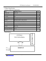
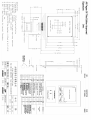
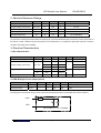
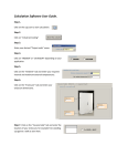
LCD MODULE SPECIFICATIONS
SPEC NO
YM128128G-3
REV NO
Good Display
Good Display
Specifications
Type:
Model No.
Standard
YM128128G-3
z 128 x 128 dots, COG LCD Module.
z With white LED backlight
z 6800/8080 series or Serial interface
Description:
Prepared:
Checked:
Approved:
Issue Date:
Xiaoli Lan
Moon Wu
Boris Jen
2008.08.01
Dalian Good Display Co., Ltd.
Good Display
No.17 Gonghua Street, Shahekou District, Dalian 116021 China
Tel: +86-411-84619565 Fax: +86-411-84619585
E-mail: [email protected]
Website: www.good-lcd.com
www.good-lcd.com.cn
Dalian Good Display Co., Ltd.
1.0
LCD Module User Manual
YM128128G-3
Table of Content
1. Basic Specifications……………………………………………………………………...…………………………………3
1.1 Display and Mechanical Specifications…………..………………………………………………..……………………3
1.2 Block Diagram…………………………...………….……………………………………………..……………………3
1.3 Terminal Functions…………………….……………………………………………...………………………………....4
1.4 Mechanical Drawing ………..………………………………………………..………………..…..…………………....5
2. Absolute Maximum Ratings………………………………………………………………..……...………………………6
3. Electrical Characteristics..……………………………………………………………………….……………….…….....7
4. IC Contents Attachment……………………………………………………………………………….……......................7
5. Design and Handling Precaution..…………….……………….…………………………….…………………………8
URL :www.good-lcd.com
page:2 of 8
YM128128G-3
LCD Module User Manual
1.0 Basic Specification
1.1 Display and Mechanical Specification
ITEM
STANDARD VALUE
UNIT
Display Type
128 X 128
Dots
LCD Type
FSTN/ Transflective/Positive
--
LCD Duty
1/128
--
LCD Bias
1/12
Bias
Viewing Direction
6:00
Clock
Backlight Type
Edge LED Backlight with white color
--
Interface
6800/8080 series or Serial Interface
--
Driver IC
S6B0741 (Gold Bump Chip)
--
IC Package
COG
--
Module Dimension
46.5(L)×56.7(W) ×4.00(H) (MAX)
mm
Visual Area
39.64(L) ×46.04(W)
mm
Dot size
0.25 ×0.30
mm
Dot Pitch
0.28 ×0.33
mm
Operating Temperature
0 ~ 50
℃
Storage Temperature
-10 ~ 60
℃
LCD Panel
128×128 Dot Matrix
VDD
VSS
S6B0741
VEE
URL :www.good-lcd.com
page:3 of 8
LED Backlight Circuit
1.2 Block Diagram
LCD Module User Manual
YM128128G-3
1.3 Terminal Functions
Pin
No.
Pin
Name
1
PS0
2
3
PS1
CSB
I/O
Descriptions
I
Parallel / Serial data input select input
H = Parallel
L= Serial
I
Microprocessor interface select input pin
-PS0=”H” ,PS1=”H” : 6800-series parallel MPU interface
-PS0=”H” ,PS1=”L” : 8080-series parallel MPU interface
-PS0=”L” ,PS1=”H” : 4 pin-SPI MPU interface
-PS0=”L” ,PS1=”L” : 3 pin-SPI MPU interface
I
Chip slect input pins
Data/ instruction I/O is enabled only when CSB is “L”. When chip
select is non- active, DB0 to DB7 may be high impedance.
4
/RES
I
Reset Signal
/RES=L, Initialization is executed
/RES=H, Normal running
5
RS
I
Register select input pin
- RS =”H”: DB0 to DB7 are display data
6
R/W(/WR)
I
/WR=L~H , /RD=H
Data or Instruction latch into the LCD module
7
/RD(E)
I
Read /Write
8-bit Data bus.,
Three state I/O terminal for display data or instruction data
When /CS=H
DB0~DB7=High Impedance
8-15
D0….D7
16
VDD
Supply
Positive Power Supply
17
VSS
Supply
Negative Power Supply, Ground(0V)
18
VOUT
I/O
19
CAP5+
O
20
CAP3+
O
21
CAP1-
O
22
CAP1+
O
23
CAP2+
O
24
CAP2-
O
25
CAP4+
O
26-30
V4-V0
I/O
31
OSC1
I
URL :www.good-lcd.com
I/O
execution control pin
Voltage converter Output
DC-DC Voltage converter capacitors terminals
LCD driver supply voltages
VDD (=Vo) ≥ V1≥V2≥V3≥V4≥VSS
When using internal clock oscillator, connect a resistor between
OSC1 and VDD
page:4 of 8
LCD Module User Manual
LED BACKLIGHT
1.4 Mechanical Drawing
URL :www.good-lcd.com
page:5 of 8
YM128128G-3
LCD Module User Manual
YM128128G-3
2. Absolute Maximum Ratings
Items
Symbol
Min
Max.
Unit
Condition
Supply Voltage (Logic)
VDD-Vss
0
+8.0
V
Vss=0V
Supply Voltage (LCD Driver)
VDD-VEE
0
16.5
V
Vss=0V
Input Voltage
VIN
0
VDD+0.3
V
Vss=0V
Operating Temperature
TOP
0
+50
℃
No Condensation
Storage Temperature
TST
-20
+70
℃
No Condensation
Cautions:
Any stresses exceeding the Absolute Maximum Ratings may cause substantial damage to the device Functional operation of
this device at other conditions beyond those listed in the specification is not implied and prolonged exposure to extreme
conditions may affect device reliability
3. Electrical Characteristics
3.1 DC Characteristics
Items
Symbol
Min
Typ.
Max.
Unit
Supply Voltage (Logic)
VDD-Vss
2.7
3.0
5.0
V
15.9
16.5
17.2
14.8
15.0
15.4
16.0
17.8
19.8
VIH
VSS+2.0
--
VDD
VIL
VSS8
--
VSS+0.8
IDD
--
0.9
--
Unit
Application pin
V
LED+
mA
LED+
Supply Voltage (LCD Driver)
VDD-VEE
Input Voltage
Logic Supply Current
Condition
-20℃
V
25℃
70℃
V
--
℃
VDD-Vss=3.0V
3.2 LED Backlight Circuit Characteristics
Items
Symbol
MIN
TYP.
MAX.
Forward Voltage
VfLED+
IfLED+
-
3.0
-
-
-
30
Forward Current
Cautions:
Exceeding the recommended driving current could cause substantial damage to the backlight and shorten its lifetime.
LED +
LED-
No. of LED = 1 x 2 = 2 Lamps
URL :www.good-lcd.com
page:6 of 8
LCD Module User Manual
YM128128G-3
4. IC Contents Attachment:
Reference Documents From SAMSUNG LCD Driver with
Contents
S6B0741
Page
1. General Description……………………………………………………P1
2. BLOCK DIAGRAM ………………………………………………….….P6
3. PIN DESCRIPTION……………………………………………..……… P13
4. FUNCTIONAL DESCRIPTION………………..…………………….... P17
5. INSTRUCTION DESCRIPTION………….…………………………….P42
6. DC CHARACTERISTICS……………………………………………….P67
7. AC CHARACTERISTICS……………………………………………….P70
8. MICROPROCESSOR INTERFACE.…………………………………..P76
URL :www.good-lcd.com
page:7 of 8
LCD Module User Manual
YM128128G-3
5. Design and Handling Precaution
1.0 The LCD panel is made by glass. Any mechanical shock (eg. dropping form high place) will damage the
LCD module.
2.0 Do not add excessive force on the surface of the display, which may cause the Display color change
abnormally.
3.0 The polarizer on the LCD is easily get scratched. If possible, do not remove the LCD protective film until
the last step of installation.
4.0 Never attempt to disassemble or rework the LCD module.
5.0 Only Clean the LCD with Isopropyl Alcohol or Ethyl Alcohol. Other solvents (eg. water) may damage the
LCD.
6.0 When mounting the LCD module, make sure that it is free form twisting, warping and distortion.
7.0 Ensure to provide enough space (with cushion) between case and LCD panel to prevent external force
adding on it, or it may cause damage to the LCD or degrade the display result.
8.0 Only hold the LCD module by its side. Never hold LCD module by adds force on the heat seal or TAB.
9.0 Never add force to component of the LCD module. It may cause invisible damage or degrade of the
reliability.
10.0 LCD module could be easily damaged by static electricity. Be careful to maintain an optimum
anti-static work environment to protect the LCD module.
11.0 When peeling off the protective film from LCD, static charge may cause abnormal display pattern. It is
normal and will resume to normal in a short while.
12.0 Take care and prevent get hurt by the LCD panel sharp edge.
13.0 Never operate the LCD module exceed the absolute maximum ratings.
14.0 Keep the signal line as short as possible to prevent noisy signal applying to LCD module.
15.0 Never apply signal to the LCD module without power supply.
16.0 IC chip (eg. TAB or COG) is sensitive to the light. Strong lighting environment could Possibly cause
malfunction. Light sealing structure casing is recommend.
17.0 LCD module reliability may be reduced by temperature shock.
18.0 When storing the LCD module, avoid exposure to the direct sunlight, high humidity, high temperature
or low temperature. They may damage or degrade the LCD module
URL :www.good-lcd.com
page:8 of 8