1
Next Generation Design of a Frequency Data Recorder Using
Field Programmable Gate Arrays
By
Bruce James Billian
Thesis submitted to the faculty of the Virginia Polytechnic Institute and State University
in partial fulfillment of the requirements for the degree of
Master of Science
in
Electrical Engineering
Dr. Yilu Liu, Chair
Dr. Richard Conners
Dr. Douglas Nelson
May 10, 2005
Blacksburg, Virginia
Keywords: Frequency Disturbance Recorder (FDR), Frequency Monitoring Network
(FNET), Power System Monitoring, Time Synchronization, Field Programmable Gate
Array (FPGA)
Next Generation Design of a Frequency Data Recorder Using Field Programmable
Gate Arrays
Bruce James Billian
Abstract
The Frequency Disturbance Recorder (FDR) is a specialized data acquisition device
designed to monitor fluctuations in the overall power system. The device is designed
such that it can be attached by way of a standard wall power outlet to the power system.
These devices then transmit their calculated frequency data through the public internet to
a centralized data management and storage server.
By distributing a number of these identical systems throughout the three major North
American power systems, Virginia Tech has created a Frequency Monitoring Network
(FNET). The FNET is composed of these distributed FDRs as well as an Information
Management Server (IMS). Since frequency information can be used in many areas of
power system analysis, operation and control, there are a great number of end uses for the
information provided by the FNET system. The data provides researchers and other users
with the information to make frequency analyses and comparisons for the overall power
system. Prior to the end of 2004, the FNET system was made a reality, and a number of
FDRs were placed strategically throughout the United States.
The purpose of this thesis is to present the elements of a new generation of FDR
hardware design. These elements will enable the design to be more flexible and to lower
reliance on some vendor specific components. Additionally, these enhancements will
offload most of the computational processing required of the system to a commodity PC
rather than an embedded system solution that is costly in both development time and
financial cost. These goals will be accomplished by using a Field Programmable Gate
Array (FPGA), a commodity off-the-shelf personal computer, and a new overall system
design.
Acknowledgements
I would like to extend a great deal of gratitude to Dr. Yilu Liu, my research advisor, for
her understanding and flexibility thought the process of working towards my degree.
Furthermore, I would like to thank Dr. Richard Conners, who helped make two years of
research endeavors both flexible and challenging. Additionally, I would like to recognize
Dr. Douglas Nelson for a great number of opportunities that he provided both applied
experience as well as a vast amount of understanding and knowledge. The opportunities
provided by Dr. Nelson throughout a large portion of my undergraduate and graduate
years at Virginia Tech offered me more experiences than all but a few students will ever
have.
I also want to thank Chunchun (Emily) Xu, Zhian (Kevin) Zhong, Jon Burgett, Jian
(Ryan) Zuo, and Lei Wang. Moreover, I would like to recognize Dr. Cameron Patterson
for his expert advice and consultation with regard to embedded systems and the Verilog
programming language.
Most important of all I would like to thank my wife, Katherine, for her understanding and
cooperation throughout the process of college, my thesis, and life.
iii
Table of Contents
Abstract ............................................................................................................................... ii
Acknowledgements............................................................................................................ iii
Table of Contents............................................................................................................... iv
List of Figures .................................................................................................................... vi
List of Tables ..................................................................................................................... vi
Chapter 1: Introduction ...................................................................................................... 1
1.1 Introduction to the Frequency Monitoring Network (FNET) ................................... 1
1.2 Needs for Improvement and Proposed Work............................................................ 3
1.3 Thesis Organization .................................................................................................. 4
Chapter 2: Current FDR Architecture................................................................................ 5
2.1 Background ............................................................................................................... 5
2.2 Analog Input Subsystem ........................................................................................... 7
2.3 Microcontroller and Computation System................................................................ 8
2.4 Timing Subsystem .................................................................................................... 9
2.5 Network Communications Subsystem.................................................................... 10
2.6 Limitations of the current FDR............................................................................... 10
2.6.1 Timing Subsystem Limitations ........................................................................ 10
2.6.2 Computation Limitations ................................................................................. 11
Chapter 3: Timing Solutions............................................................................................ 12
3.1 Background ............................................................................................................. 12
3.2 Frequency References............................................................................................. 12
3.2.1 Atomic Oscillators/Clocks ............................................................................... 12
3.2.2 Crystal Oscillators............................................................................................ 13
3.2.3 Global Positioning System (GPS).................................................................... 15
3.3 Time References ..................................................................................................... 18
3.3.1 WWVB ............................................................................................................ 18
3.3.2 Internet Time Service (ITS) ............................................................................. 20
3.3.3 Global Positioning System (GPS).................................................................... 21
Chapter 4: Next Generation FDR Overall Architecture .................................................. 23
4.1 Overview................................................................................................................. 23
4.2 Analog Subsystem .................................................................................................. 24
4.3 Computing and Networking System....................................................................... 25
4.3.1 Microcontroller system .................................................................................... 26
4.3.2 Commodity PC system .................................................................................... 27
4.4 Software architecture .............................................................................................. 29
4.4.1 Microcontroller ................................................................................................ 30
4.4.2 Commodity Off-The-Shelf (COTS) PC........................................................... 31
Chapter 5: Next Generation FDR Timing Architecture................................................... 33
5.1 Design Overview .................................................................................................... 33
5.2 Hardware Design .................................................................................................... 34
5.3 Software and HDL Design...................................................................................... 37
5.4 Limitations .............................................................................................................. 49
iv
Chapter 6: Conclusions .................................................................................................... 50
6.1 Advantages of Proposed Design ............................................................................. 50
6.2 Future Improvements .............................................................................................. 51
6.3 Final Conclusions.................................................................................................... 52
Bibliography ..................................................................................................................... 54
Appendix A: Module Descriptions .................................................................................. 56
A.1
Module Description: sample_rate_calc............................................................. 57
A.2
Module Description: pps_period_len................................................................ 59
A.3
Module Description: idiv .................................................................................. 63
A.4
Module Description: varpps_trigger ................................................................. 65
A.5
Module Description: varpps_period_len........................................................... 67
A.6
Module Description: up_counter ...................................................................... 69
A.7
Module Description: varpps_hold..................................................................... 71
A.8
Module Description: varpps_count................................................................... 73
A.9
Module Description: FNET_resolver ............................................................... 75
Appendix B: Timing FPGA Verilog Files ....................................................................... 77
B.1
Verilog Code Listing: sample_rate_calc.v........................................................ 78
B.2
Verilog Code Listing: sample_rate_calc_tb.v................................................... 79
B.3
Verilog Code Listing: pps_period_len.v........................................................... 80
B.4
Verilog Code Listing: pps_period_len_tb.v...................................................... 81
B.5
Verilog Code Listing: pps_period_len_dff.v .................................................... 82
B.6
Verilog Code Listing: pps_period_len_dff_tb.v ............................................... 83
B.7
Verilog Code Listing: pps_period_len_period_counter.v................................. 84
B.8
Verilog Code Listing: pps_period_len_period_counter_tb.v ........................... 85
B.9
Verilog Code Listing: pps_period_len_sm.v .................................................... 86
B.10 Verilog Code Listing: idiv.v ............................................................................. 89
B.11 Verilog Code Listing: idiv_tb.v ........................................................................ 90
B.12 Verilog Code Listing: idiv_tb3.v ...................................................................... 91
B.13 Verilog Code Listing: varpps_trigger.v ............................................................ 92
B.14 Verilog Code Listing: varpps_trigger_tb.v ....................................................... 93
B.15 Verilog Code Listing: varpps_period_len.v...................................................... 94
B.16 Verilog Code Listing: varpps_period_len_tb.v................................................. 96
B.17 Verilog Code Listing: varpps_period_len_tb2.v............................................... 98
B.18 Verilog Code Listing: up_counter.v ............................................................... 102
B.19 Verilog Code Listing: up_counter_tb.v .......................................................... 104
B.20 Verilog Code Listing: varpps_hold.v.............................................................. 105
B.21 Verilog Code Listing: varpps_hold_tb.v......................................................... 107
B.22 Verilog Code Listing: varpps_count.v............................................................ 108
B.23 Verilog Code Listing: varpps_count_tb.v....................................................... 109
B.24 Verilog Code Listing: FNET_resolver.v......................................................... 111
B.25 Verilog Code Listing: FNET_resolver_tb2.v ................................................. 113
B.26 Verilog Code Listing: FNET_resolver_tb3.v ................................................. 115
B.27 Verilog Code Listing: FNET_resolver_tb4.v ................................................. 117
Vita.................................................................................................................................. 119
v
List of Figures
Figure 1 – Diagram of the overall FNET system................................................................ 2
Figure 2 - Diagram of the overall FDR system................................................................... 3
Figure 3 - Structure of Version 1 of Frequency Disturbance Recorder (FDR) .................. 6
Figure 4 – Exterior view of Version 1 of the Frequency Disturbance Recorder (FDR)..... 7
Figure 5 - Structure of Version 2 of Frequency Disturbance Recorder (FDR) ................ 24
Figure 6 - Structure of version 2 FDR Timing Subsystem ............................................... 35
Figure 7 - Timing Solution FPGA function block ............................................................ 38
Figure 8 - State diagram of 1PPS detector........................................................................ 41
Figure 9 - Flowchart of 1PPS detector.............................................................................. 43
Figure 10 - Flowchart of clock divider algorithm............................................................. 47
List of Tables
Table 1 – Crystal oscillator characteristics ....................................................................... 14
Table 2 - NIST Internet Time Servers .............................................................................. 20
vi
Chapter 1: Introduction
1.1 Introduction to the Frequency Monitoring Network (FNET)
In order to monitor a complex wide area system like the power grid, a synchronized
monitoring solution had to be devised. Starting in the early 1980s, a group in Canada
devised a method for time synchronized power system monitoring [1, 2]. The problem
with this first application was that it was difficult to synchronize the clocks at the two
measurement points.
Since the original experiment, two important advancements have been made that
advanced the science of monitoring wide area electric power systems. The first
advancement is related to the synchronization for the monitoring systems. The use of the
global positioning system (GPS) allows for the easy synchronization of distant
measurement locations to within +/- 30 nanoseconds at any location on the earth [3]. The
second advancement has been the development of accurate phasor measurement
techniques in order to more accurately determine operating frequency. An example of
this type of phasor measurement technique was developed in the 1980’s and was later put
into commercial use in synchronized phasor measurement units (PMU) [4].
Building on the success of previous research which developed the world’s first PMUs,
the PowerIT group at Virginia Tech, has developed the concept of the Frequency
Monitoring Network (FNET). This network is made up of a number Frequency
Disturbance Recorders (FDR) geographically distributed throughout the three major
United States power systems. The goal of the FNET system is to provide research groups
and power system operators with near real-time information about the status of their
power systems. Additionally, the data acquired via the FNET is used to detect system
disturbances, verify power system models, and to perform post-disturbance scenario
reconstruction, among other functions [5].
1
The end goal of the FNET project is to develop a low cost, quickly deployable
synchronized PMU platform, the FDR. The deployed FDRs are time synchronized and
have high dynamic accuracy. Also, the installation costs for these units have been kept to
virtually zero. To this end, GPS is used for time synchronization, standard 120 V voltage
levels, such as those found in a typical office or home, are used for the power signal, and
proprietary frequency algorithms are used. With a system like the FNET, it has been
demonstrated that power system frequency can be accurately measured, given accurate
time synchronization, and sampling of signals at distribution voltage levels [6].
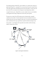
Eventually, the FNET will offer the possibility of enhancing monitoring, protection, and
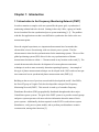
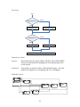
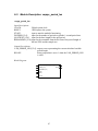
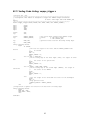
control functions for electric power systems [7]. A diagram of the FNET system can be
seen below in Fig. 1.
Figure 1 – Diagram of the overall FNET system
FDR units execute frequency calculations using algorithms of phasor analysis and signal
resampling techniques. Frequency estimation algorithms developed for FNET have
virtually no algorithm error in the frequency range of 52 Hz to 70 Hz. In the current
generation FDR, the complexity of the frequency calculations is minimized to allow the
onboard microcontroller time to complete its other tasks, such as network data output and
servicing interrupts, in order to prevent data overflow. The current version of the FDR
2
has a sampling rate of 1,440 Hz and the resulting calculated frequency accuracy is better
than ±0.0005Hz [5].
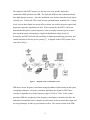
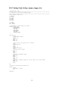
The FDR is a specialized data acquisition device specifically designed to monitor power
and frequency fluctuations in the overall power system. The device is designed such that
it can be attached by way of a standard wall power outlet to the power system. The
device then transmits its calculated frequency data through the public internet to a
centralized data management and storage server. The FDR is made up of a voltage
transducer, a low pass filter, an analog to digital converter (ADC), a GPS receiver, a
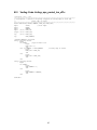
microcontroller, and a network communications module. The overall system design is
illustrated in Fig. 2.
Figure 2 - Diagram of the overall FDR system
1.2 Needs for Improvement and Proposed Work
The current generation of the FDR has a number of limitations. These include the
following: during the original system design, minimal emphasis was placed on reducing
cost; the system processor is not fast enough to process sampled data and the associated
calculations at over 1,440 samples per second. These problems prevent the current
version of the FDR from being able to address the growing needs of researchers. There is
currently a need to lower the cost per unit of the shipping FDR. At the same time,
3
researchers are looking to enhance the abilities of the FDR to handle a sampling rate of
up to 14,400 samples per second.
To address these needs, a novel solution will be presented. The solution will make use of
the increasing capabilities of programmable logic chips such as Field Programmable Gate
Arrays (FPGA). Additionally, the system will harness the rapidly increasing power of
commodity off-the-shelf personal computers for the advanced computations required of
the enhanced system. In the end, this new system will have the ability to be less
expensive than the first generation FDR while increasing the capabilities of the overall
system.
1.3 Thesis Organization
Chapter 1 has presented background information on the concept of the FNET and the
FDR, and has provided a layout of the proposed work and results of this thesis. Chapter
2 will describe the current FDR architecture. This description will provide in depth
information related to how the system is currently designed and implemented. Chapter 3
will cover timing solutions that were evaluated for the new system. Chapter 4 will
discuss the overall architecture for the next generation of FDR. Chapter 5 will cover in
detail the timing design of the new FDR system. Finally in Chapter 6, conclusions as
well as ideas for future work will be covered. Following the main body of the thesis,
there are two appendices. These appendices will cover the high level module
descriptions of the timing solution as well as the program code for the high level modules
and the underlying lower level modules.
4
Chapter 2: Current FDR Architecture
2.1 Background
Over the past few years, the PowerIT group at Virginia Tech has developed a low cost
phasor measurement unit (PMU) called a frequency disturbance recorder (FDR), in order
to monitor wide area power systems. This FDR system was built upon successful
research by Phadke, et al. [8].
The original PMUs developed at Virginia Tech by Dr. Phadke [9] and his students in the
1980’s and 1990’s directly monitored high voltage segments of the power system. This
approach provided the cleanest signal for monitoring because the PMU was physically
located at the high voltage station. The primary downside to installing the equipment at
the high voltage station was related to the cost. The installation of a PMU at a substation
was very expensive. Additionally, dedicated communications infrastructure was
required.
To address the difficulties of installing equipment at the substation, the PowerIT group at
Virginia Tech set off in a novel direction. The group concluded that rather than connect
to the high voltage power systems directly, a new system should be designed that would
enable the power signal to be monitored directly from a standard 120 V power outlet.
Furthermore, because of the rapid deployment of the public internet, the monitoring data
would be sent via internet connections rather than costly dedicated lines. This new
flexibility would allow the deployment of FDR devices virtually anywhere.
In order to measure important variables, the FDR unit executes frequency calculations
using phasor analysis algorithms. In the current generation of the FDR, the data output
rate is minimized to allow the microcontroller time to complete its other tasks, such as
network data output and servicing interrupts, and in order to prevent data overflow. The
current version of the FDR has a sampling rate of 1,440 Hz and the resulting calculated
frequency accuracy is better than ±0.0005Hz.
5
Since the FDR’s original development, over 30 units have been deployed in the PowerIT
group’s Frequency Monitoring Network (FNET) throughout the three major power
systems in the United States. The recorders have proven to be a very accurate source of
status information related to the power systems.
A comparison was made in 2003 between one FNET FDR and four commercial Phasor
Measurement Units (PMU) from different companies. The test used the PMUs and the
FDR to measure the frequency of the same phase voltage signal from a standard wall
outlet. It was clear by the collected data, that the frequency accuracy of the FDR was
very good compared to the commercial PMUs [5].
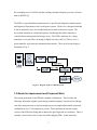
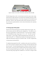
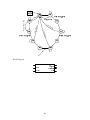
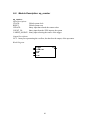
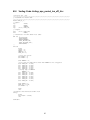
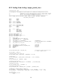
The current FDR system is made up of a number of off-the-shelf components and a
custom signal conditioning and analog to digital converter (ADC) board. As shown in
Fig. 3 below, the overall design of the system can be described in a relatively simple
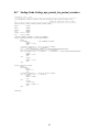
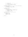
block diagram. Additionally, an exterior view of the packaged unit can be seen in Fig. 4.
The unit is packed inside of a basic 1U 19” rack enclosure with an integrated power
supply.
Figure 3 - Structure of Version 1 of Frequency Disturbance Recorder (FDR)
6
Figure 4 – Exterior view of Version 1 of the Frequency Disturbance Recorder (FDR)
The block diagram shown in Fig. 3 can be broken down into four major sections: analog
input subsystem; timing subsystem; microcontroller and computation subsystem; and the
network communications subsystem. Each of these subsystems will be described in some
detail below. Moreover, these subsystems perform specific tasks that are necessary for
the overall system operation and there is some overlap in functionality in the components
of the subsystems.
2.2 Analog Input Subsystem
The heart of the analog input subsystem is the analog to digital converter (ADC). The
ADC used in the system is an AD976A made by Analog Devices. The AD976A is a 16bit successive approximation, switched capacitor ADC. The converter has a sampling
rate of 200 kSPS and an input voltage range of -10 V to +10 V. The ADC is powered
using a single +5 V power supply, easing the integration into the overall system. The
output from the ADC is a 16-bit digital representation of the analog input signal and is
output to the FDR system controller on 16 parallel I/O lines. The ADC is integrated into
a custom printed circuit board (PCB).
To condition the input signal for the ADC, a transformer and a passive low pass filter are
used. The low pass filter is designed to filter out a majority of the input signal noise from
the power system. The nominal operating frequency of the power systems in the United
States is 60 Hz, so the low pass filter is designed to allow the lower frequency signals to
pass while rejecting the high frequency noise signals. The voltage transformer is used to
convert the analog voltage signal from a standard 120 V wall outlet to a voltage level that
7
is within the acceptable input range of the ADC. For ease of integration, the transformer
that is integrated into the power supply included with the 19” rack mount chassis was
used for the system.
2.3 Microcontroller and Computation System
At the center of the FDR is the microcontroller that controls the whole system. The
system is based around a Freescale MPC555. This 32-bit microcontroller is actually
integrated into the Axiom CME-0555 development board. This board provides easy
access to a number of peripherals on the MPC555 such as two COM ports, an LCD
interface, and memory. Additionally, the evaluation board provides a number of
connectors for easy interfacing with the complete functionality of the MPC555.
The microcontroller is used to supervise the overall operation of the whole system.
Additionally, the MPC555 generates the timing pulses that trigger the ADC to start a
conversion. This timing generation is provided by the time processor unit (TPU3) on the
MPC555. Furthermore, calculations related to the input signal frequency are completed
on the MPC555. The results of the frequency calculations are then time stamped with
time information from the GPS timing receiver. The calculated and time stamped data is
next output by the MPC555 and sent over a serial connection to the network
communications module.
The ADC sampling trigger is provided to the ADC in the form of a fixed width pulse
modulation (PWM) output from the microcontroller. Following the sample triggers that
are output to the ADC, the microcontroller receives digital representations of analog
samples back from the ADC and computes values for phase angle, frequency, and rate of
change of frequency. These values are computed using phasor techniques developed
specifically for single phase measurements [10].
8
2.4 Timing Subsystem
The timing subsystem is made up of two major components, a GPS timing receiver, and
the Time Processor Unit (TPU3) of the microcontroller. The main timing signal is
provided to the system by a GPS timing receiver. The GPS timing receiver used is the
Motorola M12+. For ease of integration, the M12+ module was actually mounted to the
evaluation board designed for the module. This evaluation board was selected because it
was prepackaged and allowed for easy integration. The receiver provided a time
reference and a time stamp.
The time reference is provided by the GPS timing receiver in the form of a 1 pulse-persecond (1PPS) signal. During operation, the rising edge of the 1PPS signal from the
receiver is synchronized to within +/- 25 ns of the absolute start of the second. This
accuracy is achieved through the synchronization of the constellation of GPS satellites
with the master clock (MC) at the United States Naval Observatory (USNO) [11].
The time stamp follows each 1PPS signal in the form of a serial data stream from the
GPS to the FDR system controller. This data stream can also include other information
including position information, and the number of satellites tracked. The decision was
made to select this receiver because once the system has achieved a three dimensional
position fix, the timing 1PPS output can still maintain its accuracy while only tracking a
single satellite. At the time this GPS was selected, there were no other GPS timing
receiver modules that were found to be able to operate with less than four satellites.
The other component of the timing subsystem is the time processor unit (TPU3) that is
embedded in the microcontroller used as the FDR system controller. The TPU3 is an
intelligent, semi-autonomous microcontroller designed for timing control. The unit can
be viewed as a special-purpose microcomputer that performs a programmable series of
operations. The operations are handled directly by the TPU3, bypassing the main system
controller, and therefore can carry out operations that would otherwise require CPU
interrupt service [12]. The embedded TPU3 provides a very powerful time and frequency
9
processing subsystem that allows for the division of the 1PPS signal into 1,440 pulses per
second.
2.5 Network Communications Subsystem
The network communications subsystem provides the gateway from the FDR system
controller to standard Internet Protocol (IP) based networks. This module converts the
data from the microcontroller into a stream of TCP data that is transmitted over the
internet to the FNET information management server (IMS). The data that is transmitted
is time stamped so the computed frequencies can be directly compared with data from
other FDRs when they are received by the FNET IMS. For the transmission, TCP was
chosen as the transport mechanism because of its fault tolerant yet reliable transmission
capabilities. Lastly, for the network communications subsystem, the modules that were
used were not common across all of the deployed FDRs. Some of the FDRs contain a
serial (RS-232) to Ethernet converter made by Moxa, while others use a converter made
by Digi. Both of these modules were found to be only marginally reliable and neither
converter worked under all circumstances.
2.6 Limitations of the current FDR
There are a number of limitations that are associated with the first generation FDR
design. There are problems related to the timing subsystem, the international
compatibility of the system, and the processing capacity of the system.
2.6.1 Timing Subsystem Limitations
Inside of the timing subsystem of the FDR, issues have been discovered that limit the
accuracy of the calculated data. These issues relate to the method in which each second
is divided into 1,440 separate time periods. As of July 2006, the timing subsystem
problem has been resolved. Furthermore, several FDRs have been successfully deployed
on 50 Hz and 220 V power systems in Europe and Africa.
10
2.6.2 Computation Limitations
Another limitation of the current generation FDR is related to the computational capacity
of the system. When the first version of the FDR was designed, a sampling frequency of
1,440 Hz was chosen, representing 24 samples per cycle of 60 cycle AC power. In order
to meet future needs of researchers the capability to handle increased sampling
frequencies will be important. In order to meet these needs, upgrades need to be made to
the embedded microcontroller in order to meet the new computing demands of the
system.
11
Chapter 3: Timing Solutions
3.1 Background
For system timing, there are two types of references that are required, frequency
references and timing references. These two references are used together to address
different portions of system synchronization. In the following chapter, the differences
between the two references and their uses will be addressed. In order to determine the
best solution for timing and frequency references, research was conducted to determine a
low cost yet reliable way to synchronize the distributed FDR systems.
3.2 Frequency References
Frequency references are used to maintain accuracy over relatively short periods of time.
These references provide higher frequency sources that allow digital systems to operate.
Different types of oscillators are used for frequency references. The different types of
oscillators have advantages and disadvantages. Two major types of oscillators are high
precision atomic clocks and crystal oscillators. These two timing sources vary greatly in
both cost and precision. High precision atomic clocks can be accurate to within 0.5 parts
per trillion (ppt) [13], whereas the best crystal oscillators (XO) are known as ovenized
crystal oscillators (OCXO) and can be accurate to within only 30 parts per billion (ppb)
[14].
3.2.1 Atomic Oscillators/Clocks
Atomic clocks are extremely accurate sources of frequency reference, however there are
a number of major drawbacks to current atomic frequency references. These drawbacks
include: the size and weight of the reference, the power consumption of the reference,
and the cost of the reference. As an example, one commercial cesium based atomic
frequency reference, the Aglient 5071A Primary Frequency Standard, is packaged in a
case that is 133.4 mm x 425.5 mm x 523.9 mm and weighs approximately 30 kg.
Additionally, this frequency standard will draw over 45 W while operating and cost over
12
US$50,000. Due to these factors, the use of atomic clocks as frequency references has a
limited number of practical applications. Additionally, with most commercial atomic
frequency references, only certain frequencies are provided. These frequencies usually
include 5 MHz and 10 MHz as well as a number of telecommunications frequency
standards. Lastly, because atomic frequency references are only frequency references,
the system still needs to be interfaced with a GPS, or another time reference, in order to
achieve long term accuracy and to provide a reference to the correct Coordinated
Universal Time (UTC).
For most applications, including the frequency reference for the FDR, the use of an
atomic frequency reference is impractical because of the cost. Furthermore, because the
commercially available frequency references only output commonly used frequencies,
and the desired frequency for the FDR is a multiple of either 1,440 or 1,200, a perfect
reference is not available. Also, the existing frequency references do not produce an
integer multiple of the desired base frequencies, therefore post-processing will still be
required to produce the desired frequency. Lastly, as stated in the previous paragraph, for
this frequency reference to provide UTC time the system would still need to be interfaced
with a time reference for the desired application.
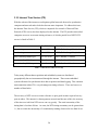
3.2.2 Crystal Oscillators
Crystal oscillators are very different from the atomic sources. Instead of using the
deterministic nature of cesium or rubidium atoms, it uses the vibration and the oscillating
surface voltage of a quartz crystal. Crystal oscillators (XO) are available in a number of
different frequencies from well below 1 MHz to over 100 MHz. These crystal oscillators
come in a variety of types. These types include standard crystal oscillators (XO),
temperature compensated crystal oscillators (TCXO), and ovenized crystal oscillators
(OCXO). The highest precision of the crystal oscillators listed, the OXCO, comes in a
range of performance levels. For the purpose of this paper OCXO will refer to standard
performance OCXOs and HPOCXO will refer to high performance OCXOs. Table 1
below summarizes the characteristics of the different crystal oscillator types.
13
HPOCXO
OCXO
TCXO
XO
Accuracy
+/- 0.01 ppm
+/- 1 ppm
+/- 1 ppm
+/- 5 ppm
short-term stability
+/- 0.000003 ppm
+/- 0.0005 ppm
+/- 0.001 ppm
N/A
Table 1 – Crystal oscillator characteristics [14]
There is a great deal of error that can be injected into a system by an oscillator, especially
by standard XOs. Factors that affect the magnitude of this error include the aging of the
oscillator, the frequency tolerance of the oscillator, and the frequency stability of the
oscillator.
Aging of a crystal refers to the overall change in frequency that is experienced by a
crystal over time. A number of factors affect aging including excessive load on the
output, thermal effects, and other factors. The aging will cause the crystal to lose
accuracy over its lifetime, such that a crystal with a nominal frequency of 10 MHz may
operate at 9,999,995 Hz after a period of time, and then continue to degrade over time. If
the system requires accurate timing, such as would be required in some radio
transmission applications, this effect can cause a number of problems if not compensated
for or dealt with appropriately.
The frequency tolerance of the crystal refers to the maximum initial allowable deviation
from the nominal value of the oscillator. This is usually expressed in parts per million
(ppm) or parts per billion (ppb) at a given temperature. The tolerance determines the
baseline level of accuracy for the oscillator. The system will never be guaranteed to
operate more accurately than the initial tolerance level.
The frequency stability of the oscillator refers to the acceptable deviation in ppm over the
rated operational temperature range. In some applications where the oscillator
experiences a great deal of temperature change, the frequency output will change over the
temperature range. To compensate for this change, the OCXO actually encapsulates the
crystal inside a temperature controlled oven to maintain a fixed temperature.
14
3.2.3 Global Positioning System (GPS)
The Global Positioning System (GPS) is made up of a constellation of 24 active satellites
orbiting approximately 20,000 kilometers above the surface of the earth. Originally
deployed by the United States Department of Defense (DoD), these satellites all have
onboard atomic clocks that synchronize to within 3 ns of the official atomic clock located
at the United States Naval Observatory (USNO). The GPS signals can be received across
the globe, anywhere that four GPS satellites can be acquired at a single time. The unique
fact that the signals from these satellites are synchronized with the atomic clock allows
end users of the system to receive synchronized frequency information.
Given that GPS uses triangulation and time data, the number of satellites in view affects
the accuracy of resulting GPS data. Initially the GPS timing receiver must acquire a fix
from four separate satellites. After a fix has been made with four satellites, the receiver
then knows its current position and can continue on with a minimum of three satellites to
maintain a position fix, and depending on the receiver, with as few as one to maintain a
frequency fix. An example of a GPS timing receiver is the Motorola Oncore M12+
Timing Receiver which needs only one satellite to maintain time accuracy.
There are a number of drawbacks to using GPS. The GPS performance can be degraded
by a number of factors and even inoperable under certain conditions. These factors
demonstrate the weaknesses of GPS as a timing or frequency reference. Many of the
factors that negatively affect GPS performance are either caused by human interference,
or can be compensated for by the end user. These factors include the intentional
degradation of the GPS signal by the United States government, and suboptimal
positioning of the GPS receiver antenna.
The intentional degradation of the GPS signal can be a source of error in the GPS system.
The degradation, also known as Selective Availability (SA), is a service controlled by the
United States DoD. It provides the U.S. DoD with the ability to degrade the performance
15
of civilian GPS receivers for national security if it is deemed necessary. Prior to May
2000, SA was permanently enabled, and therefore GPS was much less accurate, however
SA has now been indefinitely disabled.
When deploying a GPS receiver, especially a timing receiver, antenna position can make
a great deal of difference. For optimal performance, the antenna should have an
unobstructed view of the horizon in all directions. This will enable the receiver to
monitor a maximum number of satellites simultaneously and to provide a more stable
GPS lock.
On the other hand, there are number of factors that affect GPS performance that are
outside the control of humans. These factors can include atmospheric delays, signal
multipath interference, satellite geometry, and satellite orbital errors.
The atmospheric delays caused by the GPS signal traveling through the ionosphere and
troposphere can cause timing problems. These delays are caused when the signal slows
as it passes through the atmosphere. GPS receivers use an onboard model to approximate
this delay and partially correct for this, but it is not perfectly accurate.
The next factor that can degrade the GPS signal is signal multipath. Multipath occurs
when there are two or more transmission paths for a signal on its way from the GPS
satellites to the GPS receiver. The extra paths can be caused by reflection of the GPS
signal off of a building or other surface. To a certain extent, these errors can be removed
through better antenna positioning and location selection. As a caveat, when using a GPS
timing receiver, if the system is running with only one satellite acquired, this multipath
error is capable of inducing a great deal of error into the timing signal.
Satellite geometry is another factor that affects the quality of the received GPS data. The
degradation from this factor is caused by wide angles between satellites and the angle
from the receiver to the satellite. Additionally when a satellite is at a near horizontal
angle from the receiver, the signal is forced to travel through a larger slice of the earth’s
16
atmosphere and thus causes greater atmospheric errors to be received by the timing
receiver.
The last, but least important factor that can affect the GPS signal is orbital errors. These
errors are also known as ephemeris errors. They are caused when a GPS satellite is not in
the absolutely correct orbit. This error is outside of the control of the receiver and is
often considered to be negligible because of the close control of the satellites by the
ground controllers.
Overall, the drawbacks of GPS as a frequency reference are overshadowed by the
extremely accurate nature of its output. The need for a clear view of the sky and the
possibility of losing lock on the GPS system are not sufficient to cause the user of the
application described in this paper to need to upgrade to a different, more accurate
frequency reference source. At less than $100 for a GPS receiver specially designed for
timing, the balance of long term accuracy and cost of GPS is very appealing.
For the actual frequency reference the GPS timing receiver outputs a one-pulse-persecond (1PPS) signal. This 1PPS signal is very accurate. As an example, for the
Motorola M12+ GPS timing receiver, the physical 1PPS signal has a jitter of only +/-25
ns. Additionally, the receiver is able to provide a sawtooth correction that accounts for
the limited 40 MHz internal oscillator on the receiver. When the sawtooth correction is
accounted for, the resulting frequency reference can be provided with an accuracy of +/-5
ns [15].
The 1PPS output from the GPS can be coupled with a free running local crystal oscillator
to create a relatively accurate higher frequency reference. For example, if a 40 Mhz XO
were coupled with the GPS frequency reference, the resulting frequency would fluctuate
with the standard error of the XO. This error can be accounted for and compensated
through the use of a counter that can establish the number of XO ticks in the accurate
second that was provided by the GPS.
17
Additionally, the GPS receiver is not susceptible to the error that a standard XO is. The
GPS receiver is synchronized to an external satellite network reference, and because of
this, the accuracy of the reference provided is not affected by temperature, age, or system
voltage fluctuations. The resulting long term accuracy of the GPS receiver is
unparalleled in cost. Overall, a GPS timing receiver coupled with a free running low cost
XO is the most accurate and cost effective solution for the frequency reference necessary
for the FDR.
3.3 Time References
For wide area system monitoring, there is a specific need for accurate time
synchronization over a wide geographic area. From the early days of the railroad to the
current day with high precision communications equipment and power system
monitoring, the need has been present. To address this need, the United States
government (as well as other governments) provides timing references for the general
public, as well as for commercial groups. Three of these time references are detailed in
the following sections.
3.3.1 WWVB
WWVB is a system that transmits time information via a radio frequency from a base
station in the continental United States. The system, which is maintained by the National
Institute for Standards and Technology (NIST), has a base transmitter which is located
near Fort Collins in central northern Colorado. It is a 50 kW transmitter with a carrier
frequency of 60 kHz. The transmitted signal, which started transmission in its current
form in 1956, was an early time transmission standard. This standard is still used by
some groups for calibrating electronic equipment and frequency standards. WWVB
requires one minute to send its time code which includes: minute, hour, day of current
year, the last two digits of the current year, leap year and leap second indicators, daylight
savings time information and other information. WWVB is often a good choice for a
18
timing reference. The transmitted WWVB signal can be received throughout most of the
contiguous United States.
There are a number of advantages to WWVB when compared to other time references.
One advantage is that the signal can be received indoors and without a large antenna.
Another advantage is the low cost of the receiver. WWVB receivers are very
inexpensive and can be built for less than $10. These receivers are usually made up of a
simple radio interface module and a microcontroller.
The disadvantages of WWVB primarily relate to the resulting time reference accuracy.
The first factor that affects the time reference is the propagation speed of the transmitted
signal. Considering that radio waves travel at near the speed of light, and that the
transmitter is located in Colorado, it can take up to 15 ms for the signal to propagate over
the entire contiguous United States. The next factor is the path that the transmitted signal
takes. The signal has two major paths, along the ground, described as groundwave, and
reflection off the ionosphere, described as skywave. Since the path of the groundwave is
along the ground, it follows a direct path that doesn’t change length much over time.
This allows users within approximately 1,000 km of the WWVB transmitter, where the
groundwave is strong enough to be received, to compensate for the propagation delay.
With this compensation, timing accuracies of better than 100 µs can be achieved.
Beyond 1,000 km from the transmitter, the signal is mostly made up of skywave. The
skywave is less predictable than the groundwave, so compensation cannot accurately be
applied. The resulting accuracy of the received signal is limited, as described above, by
the assumed propagation delay of the signal, which yields an accuracy of within 15 ms of
the actual value time value [16].
Even though WWVB is accurate enough for many time reference applications, there are
cases where WWVB is not acceptable. In the case of the project detailed later in this
paper, the WWVB standard does not meet the requirements. The reason for this is that
the error and approximate timing accuracy of 15 ms nationwide is not acceptable for the
application.
19
3.3.2 Internet Time Service (ITS)
With the advent of the internet as a ubiquitous global network, the need to synchronize
computer and network node clocks has become more important. To address this issue,
the Internet Time Service (ITS), which is comprised of a network of Network Time
Protocol (NTP) servers, has been deployed on the internet. The ITS provides networked
computers access to an accurate timing reference, of which a partial list of NIST NTP
servers is listed in Table 2.
NAME
IP ADDRESS
LOCATION
time-a.nist.gov
129.6.15.28
NIST, Gaithersburg, Maryland
time-b.nist.gov
129.6.15.29
NIST, Gaithersburg, Maryland
time-a.timefreq.bldrdoc.gov
132.163.4.101
NIST, Boulder, Colorado
time-b.timefreq.bldrdoc.gov
132.163.4.102
NIST, Boulder, Colorado
time-c.timefreq.bldrdoc.gov
132.163.4.103
NIST, Boulder, Colorado
Table 2 - NIST Internet Time Servers [16]
Today many different data acquisition and embedded systems are distributed
geographically but are interconnected through the internet. Those same embedded
systems often need to synchronize their data acquisition and data logging. This common
interconnection makes ITS a very advantageous timing reference. There are however a
number of drawbacks.
The accuracy of NTP servers as a time reference is quite good in some respects but very
poor in others. The internet is a heterogeneous network and because of this, the accuracy
of the time received from NTP servers can vary greatly. The usual uncertainty of the
timing data is less than 100 ms. At worst, the NTP timing uncertainty can be greater than
1 s, but over time the uncertainty of a continuously running client can be less than 10 ms.
20
Additionally, the accuracy of the NTP servers can also be affected by the stratum of the
receiver. The stratum level describes what level of accuracy the source that provides
timing information to the NTP server has. With a stratum 1 NTP server, the server would
be interfaced with a primary timing source, such as an atomic clock or high accuracy
GPS timing receiver. A stratum 2 (or greater) server would, however, be interfaced with,
at best, a secondary time source.
In the application laid out later in this paper, using an NTP server as a timing reference
would be extremely easy because both the end system and the server are already
connected to the internet. Nevertheless, because the timing delay is relatively
unpredictable and large, the ITS is not a viable option.
3.3.3 Global Positioning System (GPS)
As stated in section 3.2.3, the Global Positioning System (GPS) is made up of a
constellation of satellites orbiting above the surface of the earth. The GPS signals can be
received across the globe, anywhere that four GPS satellites can be acquired at a single
time. Through the synchronization of the satellites to the atomic clock, end users of the
system can receive timing information that is nearly as accurate as the source satellites
(less than 3 ns from USNO atomic clock).
Many of the advantages and disadvantages of using GPS as a reference were described in
section 3.2.3, but there are also factors that directly affect the accuracy of the time
reference. Unaccounted for time delays in the reception of the GPS signals can cause
time errors. One example of an error that could occur is from not accounting for the
length of the antenna cable. Assume the speed of light to be 300 million m/s, an antenna
cable of 10 meters would induce a constant error of over 33ns. Additionally, when the
GPS timing receiver is using less than 4 satellites for the timing fix, signal multipath can
cause large errors.
As stated previously, the drawbacks of GPS as a timing and frequency reference are
overshadowed by the overall accurate nature of its output. At less than $100 for a GPS
21
receiver specially designed for timing, the balance of long term accuracy and cost of GPS
is second to none. For this reason, the application detailed later in this paper lays out the
use of a GPS coupled with a standard oscillator to create a very accurate variable timing
and frequency source.
22
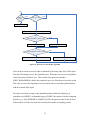
Chapter 4: Next Generation FDR Overall Architecture
4.1 Overview
Following the design and implementation of the first generation FDR, a number of
limitations were identified in the system. In order to address the shortcomings, a new
design has been formulated and the improved design will be detailed in the following
sections. This new design is aimed at increasing the accuracy, improving the flexibility
and reducing the cost of the FDR platform.
The new FDR will need to be able to handle a sampling frequency of 14,400 Hz.
Moreover, the system will need to be easily configurable for 50 Hz or 60 Hz power
systems, and for 120 V and 220 V power systems. Timing problems that were
encountered with the first version of the FDR will need to be addressed, and reliability
issues, related to the network communications module, will need to be fixed. Lastly, the
new system must achieve the same or a better price point than the pervious version.
Overall, the structure of the next generation FDR will be modified from the first
generation. Like the first generation FDR, the updated system will use a voltage
transformer and low pass filter to scale and filter the input voltage from the standard wall
outlet power signal (between 100 V and 240V). The same analog to digital converter
(ADC) will be used.
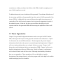
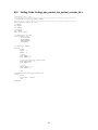
For the timing subsystem and the computation engine in the system there are a number of
changes. In order to assure the timing accuracy of the system, the GPS 1PPS signal will
be input to a Field Programmable Gate Array (FPGA). This FPGA will monitor the
incoming 1PPS signal and will send out accurate timing pulses to trigger the ADC. The
ADC will then assert an input to a smaller 16-bit microcontroller in order to indicate a
conversion has been completed. The FPGA will also indicate to the microcontroller the
start of each new second. The microcontroller will then gather the binary data from the
ADC and the GPS serial data stream and transmit it to an attached embedded PC for
23
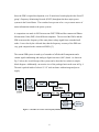
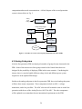
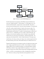
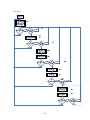
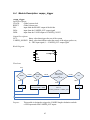
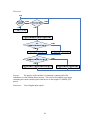
computation and network communications. A block diagram of the second generation
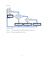
system is shown below in Fig. 5.
Analog
Input
Voltage
Timing
FPGA
Voltage
Transformer
Analog Sample Trigger
Variable PPS
1PPS
A/D
Converter
Analog
Conversion
Data
1PPS
GPS Timing
Receiver
Signal
Conditioning
GPS Serial Data
Internet
16-bit
Microcontroller
Embedded PC
Figure 5 - Structure of Version 2 of Frequency Disturbance Recorder (FDR)
4.2 Analog Subsystem
After the first generation FDR was deployed a number of groups became interested in the
FDR. Some of this interest was from groups outside of the United States that were
intrigued by the possibility of deploying FDRs in their own countries. Considering this
interest, there is a need to handle different voltage levels and different power system
frequencies in the updated FDR design.
Similar to the analog subsystem in the first generation FDR, the revised analog subsystem
will have three major components. These components include an ADC, a voltage
transformer, and a low pass filter. The ADC selection will remain the same as in the first
generation with the use of the Analog Devices AD 976A ADC. The other components
will be updated to accommodate the new international requirements on the FDR.
24
International power systems vary in voltage. Nominal voltage levels range from 100 V
up to 240 V. In order to accommodate the necessary input voltage range, the selection of
a new double tap transformer was made. The double tap transformer will enable the
selection between two voltage levels. Using both taps of the transformer in parallel will
allow voltage signals in the range of 100 V to 130V to be in an acceptable range for the
ADC, and using both taps in series will allow for use of the voltage range of 220 V to 240
V. Assuming the correct selection between the parallel or series connection, the voltage
output will be less than the -10 V to +10 V range that can be input directly into the AD
976A ADC. In addition to the transformer, the output signal will run through a simple
potentiometer based voltage divider that can be adjusted to increase the voltage accuracy
for a given deployment.
International power systems use both 50 Hz as well as the 60 Hz standard. To
accommodate this variation, the low pass filter for the input signal has to be reexamined
in order to verify correct operation with 50 Hz input signals. The verification of the
algorithm performance is not expected to show any major problems.
For both the input signal voltage and the input signal frequency, easily configurable
settings on the FDR are needed. To facilitate this, there will be 2 switches on the FDR.
The first switch will toggle the connection to the transformer from parallel to series. The
other switch will be a simple 2 position switch that will indicate to the timing subsystem
the desired nominal input signal frequency.
4.3 Computing and Networking System
With the requirement for increased accuracy and reliability for the FDR, the previous use
of a microcontroller to control all functions of the FDR and a separate serial to ethernet
converter for network operations will not be practical. To meet these new needs, changes
were made to the computation system and to the networking system of the FDR.
25
The first generation FDR was made up of a single MPC555 microcontroller that managed
all aspects of data acquisition as well as computation. That microcontroller was
connected to a serial to ethernet network interface module. It was found that the
MPC555 was nearing its maximum computational capabilities and, with the desire for a
ten-fold increase in sampling frequency, maintaining the selection of the MPC555 for all
of the computation needs was unrealistic.
To address the new needs of the system, the architecture of the computation and
networking system was changed. The new FDR alters the division of work in the system.
There are now two major components in this subsystem, a 16-bit embedded
microcontroller and a commodity off-the-shelf (COTS) personal computer (PC).
4.3.1 Microcontroller system
The 16-bit embedded processor is responsible for all of the interfacing tasks in addition to
the hard and soft real-time tasks in the system. These tasks include collecting all of the
sampling data from the ADC, including sample number, and parsing the GPS serial data
stream from the GPS timing receiver.
First and foremost, the microcontroller is responsible for collecting the ADC sample data
and correlating that data with time stamping information. To do this, the microcontroller
first receives the 1pps signal from the GPS timing receiver. The microcontroller uses this
pulse to reset an internal counter that tracks the sample number of the ADC conversion.
The microcontroller is also directly connected to the ADC. Each conversion that is
completed by the ADC is triggered by the timing subsystem (which will be described in
Chapter 5). After being triggered, the ADC executes the analog to digital conversion and
outputs the data along with a signal that indicates to the microcontroller that data is ready.
The microcontroller reads the data from the ADC and increments the internal sample
number counter. The microcontroller then stores that sample along with the
corresponding sample number in a buffer waiting to be output to the computation system.
26
In addition to receiving that data from the ADC, the microcontroller is also responsible
for receiving and parsing the serial data stream from the GPS timing receiver. This serial
data stream includes date and time data, as well as other diagnostic information such as
number of GPS satellites currently tracked. The microcontroller uses this parsed
information to determine the actual second of the day that corresponds with the sample
number that is maintained by the internal counter on the microcontroller. This time and
diagnostic information is also then stored in the transmit buffer awaiting transmission to
the computation system.
In order to transmit the data to the computation system, this microcontroller periodically
packages the data that has been stored to the transmit buffer. These data segments are
then sent to the computation system via a universal serial bus (USB) connection or
ethernet connection utilizing TCP/IP. There are a number of advantages to the use of
USB and ethernet. First, nearly every PC that is available today comes with both USB
and ethernet connectivity standard. Second, the bandwidth of both of these links far
outperforms that of the RS-232 serial bus, which was used on the first generation FDR.
The throughput of USB 2.0 (high speed) is 480 megabits per second (Mbps) and the
throughput of ethernet ranges from 10 Mbps to 1,000 Mbps. Given that the maximum
bandwidth of RS-232 is 230 kilobits per second (kbps), the use of USB or ethernet is
necessary.
4.3.2 Commodity PC system
Since the microcontroller that was previously at the heart of the FDR was running at
nearly full load, the computation engine for the system needs to be upgraded.
Considering the low cost and abundance of quality hardware systems that are based on
the Intel x86 architecture, the new system will be designed to take advantage of this
hardware. The next system will not have a costly low volume custom microcontroller or
DSP implementation inside the data acquisition (DAQ) device. Instead, as described in
the previous section, a mid-range 16-bit microcontroller will control the DAQ process
27
and will format the data and transmit it to the external x86 based PC. The data will then
be computed on the external PC. Considering the fact that commodity PCs currently
have multi-gigahertz processors onboard, the computation needs of the system will be
easily met. This will allow for a rapidly increasing amount of computational capacity in
order to address the need for oversampling in the next generation of the FNET frequency
algorithm.
Other advantages of using a commodity PC include the available peripheral interfaces.
PCs today come standard with interfaces such as USB and ethernet. Both of these
interfaces become very important when it is necessary to easily interface with high
bandwidth peripherals. In this situation, the remote DAQ device is the high bandwidth
peripheral.
Given the recent interest in computer security related issues, a commodity PC will help to
address many concerns. With the use of standard hardware comes the availability of
standard operating systems and security programs. For the FDR, the operating system
could be either Microsoft Windows XP or a standard Linux distribution. Both of these
options come with standard firewalls and are often provided with ongoing security
upgrades. The wide deployment of both of these operating systems will help to allow the
FDR system to operate in an environment where the base operating system has been
vetted millions of times over.
The lack of configurability and upgradeability was a major drawback of the first
generation FDR system. In the next generation system, all components of the system will
be easily upgradeable. Components such as the operating system software, as well as the
computation algorithm software are configurable. Also, through the use of standard PC
hardware the upgrade cycle to redesign the system with a faster main system processor
will be inexpensive and very simple. The overall upgradeability of the system enables
the FNET group to develop and test different, and more complex, frequency algorithms.
To this end, standard desktop programming tools and mathematical computation software
suites can be used to develop and deploy the algorithms.
28
After the first generation of FDR was deployed it was discovered that little remote
administration was possible once the units were installed at customer sites. To address
this issue, in the next generation FDR remote diagnostics and remote administration were
included very early in the design process. The remote administration will allow for the
FNET researchers to ease the installation of new systems and to troubleshoot nonoperational systems.
In addition to utilizing the PC for the computation part of the FDR system, the PC will
also be used for network communications. The networking support in the original FDR
was not very robust. As has been outlined in previous sections, the RS-232 to ethernet
converters that were used proved to be relatively unreliable. To address this, the
networking capabilities will be controlled by the commodity PC. Considering the wide
deployment of both Windows XP and Linux network connected machines, the
networking components of those operating systems have proven themselves to be very
robust and will enable the networking system of the FDR to be much more reliable
during long term operation. Additionally, through the use of the remote administration
features, remote diagnostics of the network systems and remote reassignment of the
systems will now be possible.
4.4 Software architecture
The design of the next generation of the FDR will be very different from the first
generation FDR in terms of software architecture. The main reason for this dramatic
change is new hardware architecture that utilizes a microcontroller as well as a COTS
PC. These two separate but complementary subsystems will need to be synchronized and
will need to communicate data to one another.
29
4.4.1 Microcontroller
The software for the microcontroller will accomplish a number of independent tasks
related to the real-time operations of the FDR system. These tasks include initial
configuration and supervisory functions, as well as reception of GPS serial stream data
and ADC sample information. The operating code that will be programmed into the
microcontroller is described in the following paragraphs.
When the microcontroller starts up, there will be a basic initialization sequence that will
configure the processor for the desired application including I/O port configuration as
well as setting other configuration registers. After the initialization process is complete
the microcontroller will then determine the operating mode of the system. The operating
mode includes the input from switches related to the selection between 50 and 60 Hz
input frequency and 120 V or 220 V input voltage.
After the microcontroller initializes itself and determines its operating state, the system
will then configure the attached FPGA. Using a stored image of the FPGA configuration
file, the microcontroller will load the configuration on to the FPGA. Using the
microcontroller to load the configuration onto the FPGA is a very important feature that
will allow the FPGA portion of the system to be updated remotely.
Once the microcontroller has been configured and has configured the FPGA, the system
will then rely on two major interrupt routines to handle the rest of the work. The first
interrupt routine is used to parse the GPS serial data stream. The serial data stream will
be input through the asynchronous serial port of the processor. As described above in
section 4.3.1, once a complete message is received and parsed, the resulting data will be
transferred to the USB transmit buffer for transmission to the COTS PC controller.
A second interrupt routine will also be running on the microcontroller. This routine
manages the data acquisition from the ADC. As will be described in the following
chapter, the ADC is triggered by the timing subsystem and the FPGA. Once the ADC is
triggered it then completes an analog to digital conversion. When the conversion is
30
complete, the ADC outputs a rising edge on the output of the BUSY pin. This BUSY
signal is routed to the microcontroller and is used to trigger the interrupt indicating a
sample from the ADC is available and valid. The interrupt then reads in the parallel data
from the ADC and increments the sample counter. In order to save the acquired
information so as to transmit it out over USB later, the microcontroller copies the sample
number and the ADC value into a buffer. Once 128 samples have been taken, the data in
the buffer is then moved into the USB transmit buffer to be transmitted to the COTS PC.
This function also has a need to recognize the start of a second. When the 1PPS output
from the GPS timing receiver is received, the following call to the ADC sample interrupt
will reset the sample number counter.
Another upgraded feature for the microcontroller in the next generation FDR is a USB
bootloader. A bootloader is a supervisory program running on the microcontroller that
allows for the internal program memory to be reprogrammed directly using the USB
connection. This feature will enable the remote updating of both the microcontroller
code and the code running on the FPGA as well. This feature will enable the FNET
researchers to continually upgrade the FDRs with more and more advanced features.
4.4.2 Commodity Off-The-Shelf (COTS) PC
The second major programmable system in the FDR will be the COTS PC. The PC will
run a standard operating system such as Microsoft Windows XP and will be responsible
for receiving data from the microcontroller systems and computing resulting power
system frequency and status information. Additionally, network transmission tasks will
be handled by the PC.
The base PC will use an operating system such as Microsoft Windows XP. As a result of
the installed base of Windows, development for the PC will be relatively easy. There are
a great number of software options available on the PC.
31
The programming for this system will be able to utilize a number off-the-shelf software
packages. These include programs such as Matlab or LabVIEW. Other options include
custom developed c or c++ programs. When compared to the complicated and limited
options that were available with the first generation FDR algorithm development, the
development options for the next generation will give researchers access to a great
number of new tools for development.
The networking for the FDR will also be managed by the PC. This task will be
accomplished through the use of the internal networking components. Many of the
computation tools have networking functionality built-in. This integrated computation
program and network access program will simplify the development cycle and will
enable the end product to be more robust and reliable.
The structure for the computation program will be relatively simple. The main
computation program will access information from the USB port via either a custom
driver or a “Communications Device Class” driver that will emulate a high speed
communications port. The computation program will then parse the incoming data and
dispatch it to the frequency calculation algorithm. The frequency calculation algorithm
will then output the frequency result to both memory and to the network system for
transmission to the FNET Information Management Server (IMS). The reason for storing
computed frequency data to memory, as well as to the network, is related to the issue of
limited bandwidth. For research purposes, having access to all 14,400 frequency
computations each second will be very valuable, but the realities of limited bandwidth
network connections must be considered. In order to minimize the network traffic, the
frequency calculations will only be sent to the IMS at 10 to 60 Hz unless otherwise
specified.
32
Chapter 5: Next Generation FDR Timing Architecture
5.1 Design Overview
The timing subsystem design will involve the use of a GPS timing receiver for both time
and frequency reference as well as a free running crystal oscillator to provide short term
period division. Additionally, a field programmable gate array (FPGA) will be used to
handle the real-time needs of the timing systems. The resulting subsystem will enable
higher accuracy timing in order to handle new multi-resampling techniques as well as the
variation between 50 Hz and 60 Hz related sampling frequencies.
The most major change for the next generation FDR was made to the timing subsystem.
In the first version of the FNET FDR, the timing for the sampling of the input signal was
managed by the time processor unit (TPU3) on board of the MPC555 microcontroller.
The TPU3 produced a pulse width modulated (PWM) signal. The result of this method
was the splitting of the second into periods that were all the same integer number of clock
ticks in length. This method created an error that would accumulate at the end of each
second and would cause errors.
The timing control system in the first version of the FDR was largely adequate for the
1,440 Hz sampling rate, but it was limited in its ability to accurately handle the ten fold
increase in sampling frequency. The reason for the problems at 14,400 Hz, is the
accumulated error from the equal length periods that divide the second. To address this
problem, an FPGA is being used to control the timing of the new system. The FPGA will
enable the error from the division of the 1 second period length divided by the desired
sample rate, to be distributed across all of the sampling pulses in a second.
Plans for future generations of the FDR will see a major accuracy boost as a result of new
sampling techniques that were recently developed. The new algorithm will use a multi
resampling (MR) technique. Through the use of the new algorithm, the frequency
calculation error can be made to reach near zero for a much wider frequency range, while
33
the current algorithm only has near zero algorithm error at 60 Hz. Several new filtering
techniques will also be used to account for signal noise at distribution level.
The advantages of this new design will include added flexibility in the timing subsystem
and the ability to offload some of the timing and synchronization from the
microcontroller. Also, the timing subsystem will no longer be restricted by what the
microcontroller counters and interrupts can handle, but will be near infinitely
configurable through the use of the configurable logic in the FPGA. The FPGA allows
for the timing system to be updated in order to handle any and all sampling frequencies
that are desired.
The second version of the FDR is designed to achieve the same goals as the first version
of the FDR but with more precision and accuracy. The revised FDR will be able to select
between 50 Hz and 60 Hz input frequency as well as 24 samples per cycle or 240 samples
per cycle. This will yield four possible sampling frequencies; 1,200 Hz, 1,440 Hz,
12,000 Hz, and 14,400 Hz samples per second. To achieve accurate sample timing at all
of these frequencies the timing subsystem will be very important.
5.2 Hardware Design
As shown below in Fig. 6, the timing subsystem of the version 2 FDR is made up of two
timing components, the GPS timing receiver and the timing FPGA, as well as two
components that receive time and frequency data, the ADC and the system
microcontroller. Additionally, two jumpers are provided that allow for the configuration
of the frequency of the input power system signal and whether 10 times multi-resampling
is desired.
34
Crystal
Oscillator
Multi-Resampling
50/60 Hz
Analog Sample Trigger
Variable PPS
Timing
FPGA
1PPS
A/D
Converter
Analog
Conversion
Data
1PPS
GPS Timing
Receiver
GPS Time
Serial Data
16-bit
Microcontroller
Figure 6 - Structure of version 2 FDR Timing Subsystem
The GPS chosen for the next generation of the FDR has not been decided but may
involve the Trimble Resolution-T. The Resolution-T is a GPS timing receiver very
similar to the Motorola M12+ used in the first version of the FDR. The switch is
necessary because the Motorola M12+ has been recently discontinued. The replacement
of the M12+ module with the Resolution-T module will be relatively simple. The
Resolution-T has nearly the same capabilities that the M12+ had. According to the
Trimble datasheet, the Resolution-T is capable of synchronizing time to within 15ns of
GPS/UTC time [17]. Additionally, the receiver outputs a similar 1PPS signal. The
Trimble receiver also has the capability to achieve a timing fix using a single GPS
satellite if the receiver has previously determined a 3-dimensional position fix. The
replacement of the Motorola M12+ with the Trimble Resolution-T will require some
modifications to the timing code due to the change in the serial data output format from
the Motorola binary protocol to the TSIP standard used by the Trimble GPS receivers.
During the initial design process an attempt was made to develop the new timing system
with a complex programmable logic device (CPLD). Once the high-level description
language (HDL) code was written and compiled, it was determined that the available
CPLD chips would not be large enough to handle the required logic. As a result, the
decision was made to move ahead with the design using a field programmable gate array
(FPGA). An FPGA is a semiconductor device that is reconfigurable at the hardware
level. The device is made up of logic blocks that can be programmed to react to
35
hardware stimuli. It is effectively a large grouping of gates on a single chip that can
accomplish any hardware configuration required. An FPGA was selected for the timing
subsystem because of its hard real-time, deterministic behavior.
For the new system we selected an FPGA from the Xilinx Spartan II family of chips. The
design is based around the selection of a Xilinx XC2S100 in the TQ 144 package. This
FPGA provides 2,700 logic cell and 100,000 total system gates [18].
The two supporting components that are accounted for in the timing subsystem layout are
the analog to digital converter (ADC) and the system microcontroller. The ADC is
triggered by the timing FPGA and the system microcontroller receives serial data
messages including timing data and GPS status information. Additionally, the 1PPS
signal from the GPS is routed to the microcontroller in order to synchronize the system to
the start of each second.
Next, in order to facilitate operation with 50 Hz and 60 Hz power systems, the FDR
needs a configuration jumper on the system. This will allow for the system to be
configured with one version of code, and then the input from the jumper will dictate how
the system operates. The jumper will provide the microcontroller and the FPGA timing
system with the current configuration state of the system. Additionally, there will be a
jumper used to select the multi-resampling mode and select between 24 samples per cycle
and 240 samples per cycle. Through the use of these jumpers the system can be
configured for the following sampling rates: 1,200 Hz; 1,440 Hz; 12,000 Hz; 14,400 Hz.
The GPS timing receiver is the heart of the timing subsystem. The GPS provides the
1PPS signal that indicates the start of each new second with a 1.0 ms wide positive pulse.
This rising edge of the 1PPS pulse is synchronized with respect to Universal Coordinated
Time (UTC) [19]. This 1PPS signal is distributed to the timing FPGA. The FPGA,
through the configurable nature of the device, then uses the period of the second to
calculate the accurate division of the second into the desired number of sample trigger
pulses for the ADC. When the ADC is triggered, a conversion is started and upon
36
completion of the conversion, the ADC sends a digital representation of the analog
sample data to the microcontroller. The microcontroller is tasked with maintaining a
counter in order to timestamp all of the incoming analog sample information. This
counter is reset based upon the rising edge of the 1PPS signal from timing FPGA.
Additionally, the GPS timing receiver provides a serial output stream containing GPS
status data and GPS timing data. The serial stream is connected directly to the system
microcontroller. The system microcontroller parses the received information and utilizes
the pertinent data. The interpreted data is then used in the determination of the final time
stamp on all analog samples.
5.3 Software and HDL Design
In order to address the bulk of the needs for the timing subsystem, a hardware time
division circuit is necessary. This hardware time division circuit is implemented through
the use of an FPGA along with compiled Verilog hardware description language (HDL)
code. Code that is produced using the Verilog compiler represents the logic required for
the timing subsystem and is used to program the operation of the FPGA.
To address the problems that were present in the fixed period divider used in the first
generation FDR, a decision was made to use a variable timing solution. This variable
timing solution will interface with a GPS and utilize an FPGA to maintain correct timing
over the course of each second.
Due to the nature of FPGAs, all of the single operations that occur during a single state
are executed in parallel. The result of this is that the actual execution of each operation is
simultaneous where as in standard microcontroller architectures, the operations would
occur in series causing a timing delay. The true hardware based real-time nature of an
FPGA provides a distinct advantage over a microcontroller based architecture for timing
operations. For comparison, when an interrupt occurs on a microcontroller, a complex
series of operations occur in order to service that interrupt. These operations include
37
completing the execution of any previously running operations, storing the program
counter in order to restart execution of the program from the point where the interrupt
was called, as well as storing all register data in the system stack to allow for retrieval of
the data after returning from the interrupt routine. Because of the serial nature of
operations execution on a microcontroller as well as the interrupt timing delays, the
delays that occur can create very negative consequences when attempting to achieve
accurate timing control.
The final FPGA system design is to have a high level Verilog module that accepts the
1PPS output from the GPS as an input and also reads in the desired input signal
frequency select line as well as the oversample select line. The module will also have
inputs from the 40 MHz system clock as well as from a global system reset controlled by
the microcontroller in the system. The main output of the module will then produce a
pulse train that distributes the error from the integer division of the period length between
two 1PPS pulses from the GPS timing receiver over the 1,200 Hz, 1,440 Hz, 12,000 Hz,
or 14,400 Hz pulses per second. A representative logic block for the FPGA module is
shown below in Fig. 7.
Figure 7 - Timing Solution FPGA function block
The FPGA block above, called the FNET_resolver, is described in Appendix A.9. This
module is the highest level Verilog module for the timing system. The code for this
timing module can be found in Appendix B.24. As is shown in the Verilog code for the
module, the module is made up of a number of submodules. These submodules carry out
the granular tasks that combine to make up the behavior of the overall system.
38
The FNET_resolver is made up of 8 major submodules. These modules are
sample_rate_calc, pps_period_len, idiv, varpps_trigger, varpps_period_len, up_counter,
varpps_hold, and varpps_count. Full descriptions of these modules can be found in
Appendix A. Additionally a submodule layout diagram can be found in Appendix A.1.
The operation of the overall FNET_resolver module is controlled through the operation
of the submodules. There are three inputs to the resolver module, not including the
system clock and the global system reset. These inputs include FREQ_SELECT,
OVERSAMPLE, and 1PPS. The outputs of the overall module include variable PPS
outputs pulses as well as indicators for the identification of the first valid 1PPS as well as
for 1PPS input errors.
The first submodule that will be discussed is the sample_rate_calc module (Appendix
A.7). This module takes the inputs FREQ_SELECT, the input which indicates the
desired input power frequency, and OVERSAMPLE, the input which indicates if 10x
oversampling is desired. The output of this module is the desired system sample rate.
The next submodule is the pps_period_len module (Appendix A.2). The purpose of this
module is to detect the 1PPS inputs and determine if the input is valid. If the input is
found to be valid, the length of the previous period will be output. Additionally, outputs
which indicate if there is an error on the 1PPS input or if the current 1PPS cycle is the
first valid 1PPS cycle that has been encountered will be output.
After the execution of pps_period_len, a trigger will be sent to the idiv submodule
(Appendix A.3). This idiv module is designed to take the 26-bit value of the previous
1PPS period length from the pps_period_len module and divide it by the 14-bit value of
the desired operating sample rate from the sample_rate_calc module. The result of the
idiv module is the integer result of the division as well as the remainder from the division
operation.
39
The varpps_trigger submodule (Appendix A.4) is the next module to be triggered. The
purpose of this module is to trigger the variable PPS length calculation on both a 1PPS
input and a valid trigger from the varpps_hold module. The outputs of the module are a
trigger which triggers the varpps_period_len module as well as an output which indicates
to the up_counter module if the trigger was caused by a 1PPS or a variable PPS output.
Following the execution of the varpps_trigger submodule, the varpps_period_len
submodule (Appendix A.5) is triggered. The task of the module is to maintain a running
total of the remainders over the duration between 1PPS triggers. This result is then used
to select the current variable pulse width length. This process is the heart of the timing
system allowing for variable pulse widths that absorb the division error of the timing
system. Once complete, the module triggers the up_counter submodule.
In order to track the length of each variable pulse period, the up_counter submodule
(Appendix A.6) is used. This module maintains a simple counter which limits the period
of the current variable pulse to the correct length. Once the counter value has been
reached, the module will then trigger the varpps_hold module.
The varpps_hold submodule (Appendix A.7) is relatively simple. The purpose of this
module is the hold the variable PPS output high for 8 clock cycles. This allows for the
signal to be held high long enough to trigger all of the modules that accept this value as a
trigger input.
The last major submodule is the varpps_count (Appendix A.8). This module is designed
to count the number of rising edges of the variable PPS output that have occurred since
the last 1PPS signal. This task is important in order to be sure that there are not more
variable PPS signals output in a given second than the desired sample rate. This protects
the system from having an extraneous pulse due to small timing irregularities. The
output of the module is sent to the varpps_trigger module for consideration during the
next system triggering.
40
The resulting operation of the FNET_resolver module is very similar to the concept of a
phase locked loop (PLL). An analog PLL was not used was because the amount of jitter
in the 1PPS signal from the GPS and the period of the 1PPS signal (1 second) causes the
time for the PLL to accurately lock to the input to be much longer than would be
acceptable for this system. Digital PLLs were also evaluated, but none were found that
would support the non-integer multiple time division the system required.
The supervisory control of the FPGA timing system is based around a sequential
synchronous state machine. Based on inputs and current state information, this state
machine directs the correct state changes for the system. In total, the state machine has 9
states which define all the steps required between global initialization through steady
state operation. A state diagram of the sequential state machine used for the timing
R
RO
CT
R_
E
_ER
R OR
CT
ER
R_
RR
OR
CTR
RO
_ER
CTR
S
&
~P
R
EV
_P
P
S
R
PP
PPS & ~PREV_PPS
module is shown below in Fig. 8.
Figure 8 - State diagram of 1PPS detector
41
The end goal of the state machine is to control the process which determines and
indicates the validity of the 1PPS input. This process has a number of steps that translate
to different states in the state machine. A detailed description of the states and the initial
processes will be given below. A flow chart for the state based control algorithm is
shown below in Fig. 9.
42
Figure 9 - Flowchart of 1PPS detector
The state machine module represented in the state diagram above, pps_sm (Appendix
B.9), is a submodule of the pps_period_len module (Appendix A.2, B.3). The
43
pps_period_len module is the overall module that detects the 1PPS inputs and determines
if the input is valid and if so, outputs the length of the previous period for use in defining
the ADC trigger period length. The length of the previous period is actually the number
of clock ticks that occur between the two prior 1PPS signals. The purpose of outputting
the previous period length is to allow the system to divide the length of the previous
second by the number of desired samples per second. This in turn will enable the system
to output equally spaced timing pulses for triggering the ADC.
When the state machine module, pps_sm, encounters a global reset input, the system is
sent to the initial state, S0. Likewise, when system counter errors occur the system also
enters state S0. While in this state, the system sets the variable PPS_ERROR to 1 in
order to indicate that an error was encountered by the 1PPS input line or when a global
initialization occurs. The state also resets the PPS_FIRST variable in order to indicate
that the first set of valid 1PPS signals has not been encountered. Other variables that are
set or reset in this state include the counter reset variable, CTR_RESET, to 1 and the
ready indicator variable (READY) to 0.
Once in the state S1, the system waits for the rising edge of a 1PPS input pulse from the
GPS timing receiver. Upon encountering the rising edge, the state machine jumps to state
S2. Following the jump, the system simply uses the 1PPS pulse as a priming pulse.
After performing the functions related to state S2, the sequential state machine then steps
to S3.
Much like the S1 state, the S3 waits for the next rising edge of the 1PPS pulse. During
state S3, the counter reset variable, CTR_RESET, is set to 0 in order to enable the clock
tick counter to start counting the length of the 1PPS interval period. During this state, the
counter value is monitored to be sure that it does not increase to greater than 40894464.
When checked, a value as high as 40894464 would indicate that a counter error had
occurred because the nominal oscillator that will be used in this system will be 40 MHz.
This error would indicate that either the 1PPS signal is unstable or the internal system
oscillator is outside its specifications. If this error condition occurs then the state will
44
return back to state S0 effectively resetting the state machine. If no errors occur and the
rising edge of the 1PPS is encountered, the system will continue to state S4.
In state S4, the system handles what will be the second valid rising edge of the 1PPS
signal input. The system concurrently sets the PPS_FIRST variable to 1 to indicate that
this is the first valid 1PPS period length that will be counted and sets the PPS_ERROR
variable to 0 to indicate the system has been primed and the 1PPS signal seems to be
valid. The system also resets the period length counter. Immediately after this state
executes, the system is moved to state S5.
After entering state S5, the system again waits for the rising edge of the 1PPS signal.
Just as in state S1 and S3, if a counter error occurs because of a period that is out of
specification, the system will jump to state S0. Otherwise, when the system encounters
the next rising edge of the 1PPS signal it continues to state S6. Once in state S6, the
system now has a valid 1PPS period length. The validity of this output is indicated by the
assertion of the READY output of the module. The internal counter is then reset in order
to accommodate the upcoming 1PPS period count. The state then immediately
transitions to S7.
During the state S7, the system once again waits for the rising edge of the 1PPS signal
and if a counter error occurs, this state will jump back to state S0. Otherwise, the system
will reset the READY output to 0 and wait for the next rising edge of the 1PPS signal at
which point it will transition to state S8.
When the system enters state S8, the steady state portion of the algorithm has been
entered. The system will now indicate that the 1PPS signal is no longer the first 1PPS
period and that the system has been fully primed and is running as intended. The state
will reset the counter in order to count the period of the next 1PPS period. Additionally,
this state will output the number of clock ticks between the last two 1PPS signals by
asserting the READY line. Once completed, the system will move to state S9.
45
State S9 is the steady state wait state. This state waits for the rising edge of the 1PPS
signal. As has been covered in previous wait states, if a counter error occurs during this
state the system will return to state S0. If another valid 1PPS signal is encountered, the
system will jump to state S8 and will enter the steady state loop that will continue until
there is a 1PPS period length error.
The requirement of the clock division algorithm programmed into the FPGA is to divide
the period between two 1PPS pulses into a defined number of sampling periods. The
problem with this requirement is that the clock signal being input to the system, under
most all conditions, will not be an integer multiple for the desired number of periods. As
described in the previous sections, this causes the possibility of a great deal of error
during the last period of the second. To address this issue, the idea of using a variable
pulse period was considered. If the period is divided and there is a remainder that is not
zero, the system will automatically add 1 clock period to the length of certain periods in
order to distribute the error caused by the remainder of the division.
The core of the algorithm for the clock division is shown below in Fig. 10 in a flowchart.
This algorithm is programmatically located at the heart of the varpps_period_len module
described in Appendix A.5 and B.15. Overall, the basic concept of the design is
relatively straightforward: vary the period of the pulses over the course of each second in
order to distribute the error.
46
Entry
Rising edge of
RESET
FALSE
Rising edge of start
FALSE
TRUE
TRUE
PREV_REMAINDER = 0
CURR_REMAINDER = REMAINDER + PREV_REMAINDER
If
CURR_REMAINDER > SAMPLE_RATE
FALSE
TRUE
VAR_PERIOD_LEN = QUOTIENT + 1
VAR_PERIOD_LEN = QUOTIENT
If
CURR_REMAINDER >= SAMPLE_RATE
FALSE
TRUE
PREV_REMAINDER = CURR_REMAINDER – SAMPLE_RATE
PREV_REMAINDER = CURR_REMAINDER
Figure 10 - Flowchart of clock divider algorithm
At the start of each new second, which is indicated by the rising edge of the 1PPS signal
from the GPS timing receiver, the algorithm resets. When the reset occurs, the algorithm
clears the internal variable it uses. This variable is the previous remainder
(PREV_REMAINDER) which is the remainder carry over from the previous time period.
This value is reset at the beginning of each second in order to maintain synchronization
with the external 1PPS signal.
The other values that are input to the algorithm module include the following: an
algorithm reset (RESET), an algorithm trigger (START), the number of desired sampling
periods (e.g. 1,440) (DIVIDER or SAMPLE_RATE), the quotient value for the division
of the number of clock ticks in the last second by the number of sampling periods
47
(QUOTIENT), and remainder of the operation that provided the QUOTIENT value
(REMAINDER).
The module is triggered to start by the rising edge of the START input to the module.
This START input is provided by a combination of the 1PPS signal and the pulse at the
end of each sample time period. The algorithm is then designed to check if the current
accumulated remainder, which is the sum of the PREV_REMAINDER value and the
REMAINDER value that was input to the algorithm, is greater than the DIVIDER, or
sample rate. If the current remainder is not larger than the sample rate, then the period
length for this iteration will be the base QUOTIENT value. If the current remainder is
larger than the sample rate, then the period length will be set to be the base QUOTIENT
plus 1, creating an extended period. As a result the integer division remainder
accumulation will be completely accounted for and distributed throughout the second.
Finally, the algorithm checks to see if the current remainder value is greater than or equal
to the DIVIDER. If the current remainder value is found to be greater than or equal to
the previous remainder, which will be carried into the next iteration of the algorithm, it
will be set to be the current remainder minus the sample rate or DIVIDER. Meanwhile, if
the current remainder is less than the sample rate then the previous remainder will be set
to be equal to the current remainder. As a result of this algorithm the remainder error
caused by the integer division of the number of clock ticks between the last two 1PPS
signals will be distributed throughout the pulses during the next second.
In order to verify the operation of these algorithms, a number of Verilog test benches
were created. The test benches to test the period divider algorithm are located in
Appendix B.16 and B.17. Both of these test benches tested the algorithm on a shortened
time period. The reason for this is related to the length of time required to simulate the
system for a full 1 second. Additionally, test benches for the complete system can be
found in Appendix B.25 through B.27. The test bench located in B.27 tests the system on
a real world time scale. Be aware that depending on the simulation program and
computer used, less than 10 seconds of real time can take over 12 hours. Test benches
for various other modules are also included in Appendix B.
48
5.4 Limitations
The speed of the input oscillator that is used to break up the 1PPS period is only 40 MHz.
The chosen oscillator limits the system because it adds to the possible jitter of the system.
Since the smallest possible increment that can be made to the output pulse is 1 clock
cycle, the minimum jitter would be +/- 25ns. This could be decreased by improving the
system to operate from a higher speed oscillator.
There is also an approximately 5 ns to 10 ns offset error in the 1PPS arrival time. This
causes the 1PPS to arrive at the output of the GPS up to 10ns after the actual start of the
second in absolute time. This error is caused by propagation delays in the chosen GPS
receiver. This error is common with all GPS timing receivers of the type previously
chosen, the Motorola Oncore M12+ Timing Receiver. This error is a fixed error and can
be filtered out by post processing the resultant data.
Even though the next generation timing subsystem will be a great improvement over the
current timing control method, there are still some limitations to the new FPGA design.
All of the registers inside of the FPGA have a fixed size. The module was designed to
run from a 40 MHz clock with the only selectable frequencies being 1,200 Hz, 1,440 Hz,
12,000 Hz, and 14,400 Hz as described above. Since the input clock signal is monitored
for accurate period length, by checking that the input clock signal is within +/- 2% of 40
MHz without modification the system cannot be run with a faster oscillator. The system
is designed such that if the Verilog programming code written for the FPGA is modified
and recompiled, the system would be able to handle up to a 60 MHz source clock.
49
Chapter 6: Conclusions
Overall, the revised design for the FDR will provide for a greater level of adaptability for
researchers. With the new capacity for expanded applications, researchers will be able to
achieve new levels of accuracy.
6.1 Advantages of Proposed Design
The design that was presented in this paper has a number of advantages over the previous
generation of the FDR design. The first generation design was improved with increased
capabilities, reliability, flexibility, and affordability.
The capabilities of the first generation FDR system were upgraded in the proposed
design. The first example of this is the increase in timing and frequency accuracy.
Through the use of a variable period timing pulse, errors that previously accumulated will
now be distributed throughout all of the pulses. In the end, this distribution of the error
will lead to improved timing and frequency performance.
The capabilities were also enhanced through the use of new higher sampling frequencies.
The new system will have the capability to capture ten times the number of samples that
the first generation system captured during each second. With this increased data flow
also came the need for a higher performance computation engine. To meet this need, a
commodity off-the-shelf PC has been selected to process the computations for the new
FDR system. The PC will allow the researchers to harness the rapidly increasing
computation power of consumer hardware as well as reap the benefits of the stiff
competition in the PC market through lower prices for hardware.
Through the use of the PC that was described in the previous paragraph, network
communications will become more reliable. Using commercially available operating
systems and user software, the proposed design will build on the networking reliability of
those software packages rather than attempting to reinvent those systems. Additionally,
50
the new design will provide diagnostic information for remote troubleshooting of
deployed hardware. These remote diagnostics will include data such as the number of
GPS satellites tracked and will allow researchers to immediately diagnose common
problems.
In order to increase the usefulness of the proposed design to researchers, increased
flexibility was included. This flexibility enables the FDR systems to be deployed on
international power systems. In order to be deployed internationally, the system will be
able to support 50 Hz and 60 Hz power systems as well as 120 V and 220 V power
systems. On top of this, the ability for ten times oversampling will increase the
usefulness of the acquired data for researchers.
The last major category of improvement made in the proposed FDR design was related to
the cost of the system. The first generation FDR included a demonstration board for the
MPC 555 microcontroller that alone cost nearly US$600. This added dramatically to the
overall system cost and negatively impacted the FDR system’s ability to remain under
US$1000 in total. Through the use of a more simple architecture and by moving away
from the use of demonstration boards, the proposed FDR design will reduce the overall
system cost dramatically. This cost reduction will enable more units to be deployed and
more data to be recorded for analysis.
6.2 Future Improvements
Although a number of enhancements to the design of the first generation FDR have been
detailed in this paper, there are still a number of improvements that can be made to this
system in the future. Some of the improvements are related to the hardware in the system
and some are related to the software.
The accuracy of the GPS 1PPS can be adjusted to be as accurate as +/- 5 ns when
accounting for the “sawtooth error”. In order to take advantage of this increased
accuracy, a faster oscillator would increase the precision of the overall timing and
frequency system. Assuming a 5 ns error is the best that the system can achieve, a 200
51
MHz clock would then produce the best results that could be practically achieved. By
increasing the clock speed for the system, the magnitude of the jitter would be decreased
to +/- 1 clock period of the 200 MHz oscillator, or +/- 5ns.
To handle a 200 Mhz clock, the timing subsystem would have to be updated to include
larger counting registers. As a result of the larger counting registers, it would take nearly
the same effort to implement a fully adjustable clock divider. The new divider could
accept inputs specifying the complete desired sample rate, rather than limiting the user to
4 discreet sample rates. This would extend the future usefulness of the timing module.
Additionally, more simulation and testing would be required to verify that the current
Verilog code would work for a 200 MHz system clock speed. Lastly, there is a
possibility that a faster speed grade of FPGA chip would need to be selected.
A standalone module for the timing subsystem could be constructed. This would allow
the research group to have a single module that could be used for many different accurate
timing needs. This module would have an FPGA and its associated memory circuitry, an
oscillator, and a GPS timing receiver on it.
Hardware validation of the described timing module was not performed during the
preparation of this paper. Even though the program code worked in the simulation
environment, there is nothing more absolute than testing the system in hardware. This
verification would allow the research group to characterize this timing and frequency
source to validate its accuracy and precision. To do this, a high precision source such as
a calibrated frequency counter or digital logic analyzer will necessary.
6.3 Final Conclusions
Based on the information presented in this thesis, one should be able to design, build and
test a timing module as described. While further testing is recommended, it is felt that
with the currently described system, an accurate and robust timing solution should be
deployable.
52
In the future the total equipment cost for manufacturing the FDR will continue to
decrease. As the prices drops, deployment of this research platform on a very large scale
will become much more realistic. With this future rollout, extensive realtime information
can be gathered about the status of the power systems to which the FDRs are attached.
This data will continue to provide researchers with a wealth of new research
opportunities for the foreseeable future.
53
Bibliography
[1]
Missout, G. and Girard, P., “Measurement of Bus Voltage Angle between
Montreal and Sept-Iles,” IEEE Transactions on PAS, vol. PAS-99, no. 2,
pp. 536-539, March/April 1980.
[2]
Bonanomi, P., “Phase Angle Measurements with Synchronized Clocks –
Principle and Applications,” IEEE Transactions on PAS, vol. PAS-100,
no. 12, pp. 5036-5043, December 1981.
[3]
Hambley, R., Clark, T., “Critical Evaluation of the Motorola M12+ GPS
Timing Receiver vs. the Master Clock at the United States Naval
Observatory, Washington, DC,” 34th Annual Precise Time and Time
Interval (PTTI) Meeting, Reston, VA, 2002.
[4]
Phadke, A. G., Thorp J., and Adamiak, “A New Measurement Technique
for Tracking Voltage Phasors, Local System Frequency, and Rate of
Change of Frequency,” IEEE Transactions on PAS, May 1983.
[5]
Zhong, Z., Xu, C., Billian, B., Zhang, L., Tsai, S., Conners, R., Centeno,
V., Phadke, A., and Liu, Y., “Power system Frequency Monitoring
Network (FNET) Implementation,” IEEE Transactions on Power Systems,
vol. 20, no. 4, pp. 1914-1921, November 2005.
[6]
Hashiguchi, T., Yoshimoto, M., Mitani, Y., Saeki, O., and Tsuji, K.,
“Analysis of Power System Dynamics Based on Multiple Synchronized
Phasor Measurements,” 2003 IEEE Power Engineering Society General
Meeting, vol. 2, pp. 615-620, July 2003.
[7]
Burnett, R. O., Jr., Butts, M. M., Cease, T. W., Centeno, V., Michel, G.,
Murphy, R. J., and Phadke, A.G., “Synchronized phasor measurements of
a power system event,” IEEE Transactions on Power Systems, vol. 9, no.
3, pp. 1643-1650, August 1994.
[8]
Phadke, A. G., “Synchronized Phasor Measurements in Power Systems,”
IEEE Computer Applications in Power, pp. 10-15, April 1993.
[9]
Phadke, A. G., “Synchronized Phasor Measurements – A Historical
Overview,” Transmission and Distribution Conference and Exhibition
2002: Asia Pacific, vol. 1, pp. 476-479, Oct 2002.
[10]
Chen, J., “Accurate frequency estimation with phasor angles”, Master
thesis, Virginia Polytechnic Institute and State University, 1994.
54
[11]
“USNO GPS Time Transfer,” United States Naval Observatory,
http://tycho.usno.navy.mil/gpstt.html, May 10, 2005.
[12]
“MPC555 / MPC556 User’s Manual,” Freescale Semiconductor, Inc.,
Phoenix, AZ, Oct. 2000.
[13]
“Symmetricom 5071A – Primary Frequency Standard Datasheet,”
Symmetricom, Inc., San Jose, CA, 2005.
[14]
Munford, P.J., “Relative timing characteristics of the one pulse per second
(1PPS) output pulse of three GPS receivers,” The Sixth International
Symposium on Satellite Navigation Technology Including Mobile
Positioning & Location Services, Melbourne, Australia, Jul. 2003.
[15]
“M12+ GPS Receiver User’s Guide,” Synergy Systems, San Diego, CA,
2002.
[16]
NIST Special Publication 432, NIST Time and Frequency Services,
Lombardi, Michael A., 2002.
[17]
“Resolution T Datasheet,” Trimble Navigation, Inc., Sunnyvale, CA,
2006.
[18]
“Spartan-II 2.5V FPGA Family: Complete Data Sheet,” Xilinx, Inc., Aug.
2005.
[19]
“Resolution T System Designer Reference Manual,” Trimble Navigation,
Inc., Sunnyvale, CA, 2005.
55
Appendix A: Module Descriptions
56
A.1
Module Description: sample_rate_calc
sample_rate_calc:
Input description:
FREQ_SELECT:
OVERSAMPLE:
binary input for selecting input signal frequency
0 = assume input signal is 50 Hz
1 = assume input signal is 60 Hz
binary input for selecting oversample mode
0 = use 1x sampling, sample at 24 samples/cycle
1 = use 10x oversampling, sample at 240 samples/cycle
Output description:
SAMPLE_RATE [13:0]:
14-bit output vector representing the actual sampling rate
for the system. This value can be determined by the
following multiplication:
FREQ_SELECT cycles 24 * (OVERSAMPLE ) samples
*
cycle
second
Block Diagram:
57
Flowchart:
Entry
FREQ_SELECT = 0
FALSE
TRUE
FREQUENCY = 50
OVERSAMPLE = 0
FREQUENCY = 60
FALSE
TRUE
OVERSAMPLE = 1
OVERSAMPLE = 10
SAMPLE_RATE = 24 * (FREQUENCY) * (OVERSAMPLE)
Dependencies: None
Purpose:
This module takes two inputs, FREQ_SELECT and OVERSAMPLE.
These two inputs define the sampling rate of the analog input to the
overall system.
Limitations:
This module can only be used for 50 Hz and 60Hz inputs. Also, this
module only supports no oversampling and 10x oversampling.
Submodule layout:
58
A.2
Module Description: pps_period_len
pps_period_len:
Input Description:
CLOCK:
Global system clock
RESET:
Global system reset
PPS:
1PPS (pulse per second) input to system
Output Description:
PERIOD_LEN [25:0]:
PPS_ERROR:
PPS_FIRST:
READY:
26-bit output vector representing the number of clock
cycles between the last two valid 1PPS inputs
binary value indicating an error with the 1PPS input. This
can be set high by a loss of the 1PPS signal or a 1PPS
period that is too long. This value will be set low after the
rising edge of the second 1PPS after an error or reset
binary value indicating that the current 1PPS period is the
first valid and counted period. The output will go high
after the rising edge of the second 1PPS and go low after
the rising edge of the fourth 1PPS
binary value indicating that the output data is valid; 1 =
ready, 0 = not ready
State Machine:
59
S
&
~P
R
EV
_P
P
S
R
PP
_ER
RO
_ER
CTR
CTR
R OR
PPS & ~PREV_PPS
ER
R_
CT
R
RO
CT
R_
E
Block Diagram:
60
RR
OR
Flowchart:
61
Dependencies:
module dff
module period_counter
module pps_sm
Purpose:
The main purpose of this module is to detect the 1PPS inputs and
determine if the input is valid, and if so, output the length of the previous
period. Additionally, this module outputs PPS_ERROR and PPS_FIRST,
which indicate when an error has been encountered with the 1PPS signal
and when the first valid series of pulses is begin sent out, respectively.
Limitations:
state.
The system must see three 1PPS inputs before it will get out of the error
62
A.3
Module Description: idiv
idiv:
Input Description:
CLOCK:
START:
DIVIDEND [25:0]:
DIVIDER [13:0]:
Output Description:
QUOTIENT [15:0]:
division
REMAINDER [13:0]:
READY:
Global system clock
input used to initiate the integer division operation on a rising edge
the dividend used in the division operation
the divider used in the division operation
16-bit output vector indicating the quotient result of the
14-bit output vector indicating the remainder of the division
the binary output that indicates when the quotient and
remainder are valid
Block Diagram:
DIVIDEND [25:0]
QUOTIENT [15:0]
DIVIDER [13:0]
REMAINDER [13:0]
START
READY
CLOCK
63
Flowchart:
Entry
BIT = 0
and
START =1
TRUE
BIT = 26;
QR = DIVIDEND;
FALSE
BIT = 0
and
START = 0
FALSE
TRUE
Do Nothing
DIFF = QR[39:25] - DIVIDER
DIFF[26]
FALSE
TRUE
QR = QR<<1;
QR = {DIFF[13:0], QR[24:0], 1'd1}
BIT = BIT -1;
Purpose:
The purpose of this module is to take a 26-bit value (DIVIDEND) and
divide it by a 14-bit value (DIVIDER). The results of this operation are
ready 26 clock cycles after the assertion of the START input.
Limitations:
Since this module can only output a 16-bit quotient result, the expected
dividend and divider must not produce a result that is larger than 65535
(216). Also, the results of the operation are not available for 26 clocks
cycles from the rising edge of the START input.
64
A.4
Module Description: varpps_trigger
varpps_trigger:
Input Descriptions:
CLOCK:
Global system clock
RESET:
Global system reset
IN1:
input from the READY output of the divider
IN2A:
input from the VARPPS_OUT output signal
IN2B:
input from the VALID output of VARPPS_COUNT
Output Descriptions:
OUT:
binary value that triggers the rest of the system
VARPPS_SOURCE: binary value that indicates what the source of the trigger pulse was;
0 = 1PPS input signal; 1 = VARPPS_OUT output signal
Block Diagram:
Flowchart:
Entry
FALSE
RESET
TRUE
Rising edge of
1PPS
FALSE
Rising edge of
VARPPS_OUT
and
VARPPS_VALID = 1
TRUE
FALSE
else
TRUE
TRUE
OUT = 0;
Purpose:
OUT = 1;
VARPPS_SOURCE = 1PPS;
OUT = 0;
OUT = 1;
VARPPS_SOURCE = VARPPS_OUT
This module is designed to trigger the VARPPS length calculation on both
a 1PPS input and valid VARPPS_OUT inputs.
65
Limitations:
None
66
A.5
Module Description: varpps_period_len
varpps_period_len:
Input Descriptions:
CLOCK:
Global system clock
RESET:
1PPS input to the system
START:
input to start the modules functioning
DIVIDER [13:0]:
input for the number of periods to split the 1 second period into
QUOTIENT [15:0]: input for the base length for the split period
REMAINDER [13:0]: input for the remainder from the division of the period length of
the last 1PPS and the sample rate
Output Descriptions:
VAR_PERIOD_LEN [15:0]: output vector representing the current calculated variable
period length
READY:
binary output that is set to 1 when the VAR_PERIOD_LEN
is valid
Block Diagram:
QUOTIENT [15:0]
VAR_PERIOD_LEN [15:0]
DIVIDER [13:0]
READY
REMAINDER [13:0]
START
RESET
CLOCK
67
Flowchart:
Purpose:
The purpose of this module is to maintain a running total of the
remainders over the duration between resets. The result of this module is an output
containing the current variable pulse width for use in the length of VARPPS_OUT
period.
Limitations:
Vector lengths input signals.
68
A.6
Module Description: up_counter
up_counter:
Input Descriptions:
CLOCK:
RESET:
UPDATE:
COUNT_IN:
VARPPS_SOURCE:
Global system clock
Global system reset
binary input that reloads the counter value
binary input from the 1PPS input to the system
binary input selecting the source of the trigger
Output Descriptions:
OUT: binary out representing the overflow, the therefore the output, of the upcounter
Block Diagram:
69
Flowchart:
Entry
If rising edge
RESET
FALSE
TRUE
OUT = 0
DATA = 0
Rising edge
UPDATE
FALSE
TRUE
Trigger from
1PPS
FALSE
DATA == 0
TRUE
OUT = 0
DATA = COUNT_IN - 38
FALSE
TRUE
OUT = 0
DATA = COUNT_IN - 10
OUT = 1
DATA = DATA - 1
Dependencies:None
Purpose:
The module is a modified basic down counter with load and reset. The
count of the module is reset on the rising edge of RESET and updated on
the rising edge of UPDATE. The update of the counter is based on the
source of the trigger. The reason for this variable update is because of the
time delays in other parts of the system. If the source of the trigger is
from the 1PPS then there is a 38 clock cycle delay, whereas if the source is
a follow up trigger from the VARPPS_OUT then the delay is 10 clock
cycles. The output of the module is set high when the counter has counted
down to the zero
Limitations:
Only has a 16-bit max count value so the module is limited to counting
down from 65535.
70
A.7
Module Description: varpps_hold
varpps_hold:
Input Descriptions:
CLOCK:
RESET:
VARPPS:
PPS:
PPS_ERROR:
Global system clock
Global system reset
binary input from the VARPPS_OUT signal
1PPS (pulse per second) input to system
binary input indicating an error on the PPS input
Output Descriptions:
PULSE OUT: binary output that is the main output from the system representing the
variable PPS output
Block Diagram:
71
Flowchart:
Entry
FALSE
If rising edge
RESET
TRUE
PULSE_OUT = 0
COUNT = 0
Rising edge PPS
or
Rising edge VARPPS
FALSE
TRUE
COUNT == 0
FALSE
TRUE
PULSE_OUT = 1
COUNT = 8
PULSE_OUT = 0
COUNT = 0
PULSE_OUT = 1
COUNT = COUNT - 1
Dependencies: None
Purpose:
This module holds the variable PPS output high for 8 clock cycles
Limitations:
Only holds output high for 8 clock cycles
72
A.8
Module Description: varpps_count
varpps_count:
Input Descriptions:
CLOCK:
Global system clock
RESET:
1PPS input to the system
VARPPS:
the variable PPS output signal of the system
SAMPLE_RATE[13:0]:
the sample rate the that system is running at
Output Descriptions:
VALID:
binary value indicating that the SAMPLE_RATE number of VARPPS
signals has not been exceeded.
Block Diagram:
Flowchart:
Entry
If rising edge
RESET
FALSE
TRUE
SAMPLES_REMAINING == 1
TRUE
FALSE
Rising edge
VARPPS
FALSE
TRUE
VALID = 1
SAMPLES_REMAINING = SAMPLE_RATE
VALID = 0
Dependencies:
73
VALID = 1
SAMPLES_REMAINING =
SAMPLES_REMAINING - 1
Purpose:
This module counts the number of rising edges of VARPPS since the last
1PPS signal. This count is used to be sure that there are not more variable
PPS signals outputted than should have been in a single second
Limitations:
Can only maintain the count if the maximum count number is less than
16383.
74
A.9
Module Description: FNET_resolver
FNET_resolver:
Input Descriptions:
CLOCK:
RESET:
FREQ_SELECT:
OVERSAMPLE:
1PPS:
Global system clock
External reset signal to the system
External input that selects between 50 Hz and 60 Hz operation
External input that selects between 1x and 10x oversampling
External input from the GPS timing receiver indicating the start of
each second
Output Descriptions:
VARPPS_OUT:
output indicating the variable PPS pulse with the error distributed
throughout the pulse train
FIRST:
output indicating that the current second is the first valid second
for data acquisition
ERROR:
output indicating an error with the 1PPS input
Block Diagram:
1PPS
VARPPS_OUT
FREQ SELECT
OVERSAMPLE
RESET
FIRST
CLOCK
ERROR
Dependencies: sample_rate_calc
pps_period_len
idiv
varpps_trigger
varpps_period_len
up_counter
varpps_hold
varpps_count
Purpose:
This module takes an input from the 1PPS (pulse per second) output of a
timing GPS receiver. The module then divides the period of the second
into a number of periods that are roughly the same. By roughly, it is
meant that the error of the non-integer divide is distributed through out the
pulse train. Therefore, some of the pulses in the pulse train are 1 clock
period longer than the base period so as to make up for non-integer divide
75
remainder. Overall the function of this module is similar to a clock
divider
Limitations:
The output pulse train will have a +/- 1 clock period jitter in the output
timing signal.
76
Appendix B: Timing FPGA Verilog Files
77
B.1
Verilog Code Listing: sample_rate_calc.v
`timescale 1ns / 1ps
////////////////////////////////////////////////////////////////////////////////
// Description: This module takes two inputs, FREQ_SELECT and OVERSAMPLE.
//
These two inputs define the sampling rate of the analog input
//
to the overall system
////////////////////////////////////////////////////////////////////////////////
module sample_rate_calc(FREQ_SELECT, OVERSAMPLE, SAMPLE_RATE);
input
input
FREQ_SELECT;
OVERSAMPLE;
//0=50Hz, 1=60Hz
//0=1x, 1=10x
output [13:0] SAMPLE_RATE;
reg
[13:0] SAMPLE_RATE;
always @(FREQ_SELECT or OVERSAMPLE)
begin
case ({FREQ_SELECT, OVERSAMPLE})
2'b00 : SAMPLE_RATE = 14'd1200;
2'b01 : SAMPLE_RATE = 14'd12000;
2'b10 : SAMPLE_RATE = 14'd1440;
2'b11 : SAMPLE_RATE = 14'd14400;
//default : $display("Invalid Sample
endcase
end
endmodule
78
//50Hz with NO oversampling
//50Hz with oversampling
//60Hz with NO oversampling
//60Hz with oversampling
Rate Select");
B.2
Verilog Code Listing: sample_rate_calc_tb.v
`timescale 1ns / 1ps
////////////////////////////////////////////////////////////////////////////////
// Description: Testbench for sample_rate_calc
////////////////////////////////////////////////////////////////////////////////
module sample_rate_calc_tb_v;
// Inputs
reg
reg
FREQ_SELECT;
OVERSAMPLE;
// Outputs
wire
[13:0] SAMPLE_RATE;
// Instantiate the Unit Under Test (UUT)
sample_rate_calc uut (
.FREQ_SELECT(FREQ_SELECT),
.OVERSAMPLE(OVERSAMPLE),
.SAMPLE_RATE(SAMPLE_RATE)
);
initial
begin
// Initialize Inputs
FREQ_SELECT = 0;
OVERSAMPLE = 0;
// Wait 100 ns for global reset to finish
#100;
//simulate 60 Hz and 1x oversample
FREQ_SELECT = 1;
OVERSAMPLE = 0;
//result should be 1440
#100;
//simulate 60 Hz and 10x oversample
FREQ_SELECT = 1;
OVERSAMPLE = 1;
//result should be 14400
#100;
//simulate 50 Hz and 1x oversample
FREQ_SELECT = 0;
OVERSAMPLE = 0;
//result should be 1200
#100;
//simulate 50 Hz and 10x oversample
FREQ_SELECT = 0;
OVERSAMPLE = 1;
//result should be 12000
end
endmodule
79
B.3
Verilog Code Listing: pps_period_len.v
`timescale 1 ns / 1 ps
////////////////////////////////////////////////////////////////////////////////
// Description: The main purpose of this module is to detect the 1PPS inputs and
//
determine if the input is valid, and if so, output the length
//
of the previous period. Additionally, this module outputs
//
PPS_ERROR and PPS_FIRST, which indicate when an error has been
//
encountered with the 1PPS signal and when the first valid series
//
of pulses is begin sent out, respectively
////////////////////////////////////////////////////////////////////////////////
module pps_period_len(CLOCK, RESET, PPS, READY, PERIOD_LEN, PPS_ERROR, PPS_FIRST);
input
input
input
CLOCK;
RESET;
PPS;
output
READY;
wire
READY;
output [25:0] PERIOD_LEN;
wire
[25:0] PERIOD_LEN;
output
PPS_ERROR;
wire
PPS_ERROR;
output
PPS_FIRST;
wire
PPS_FIRST;
wire
wire
wire
[9:0]
state;
CTR_ERROR;
[25:0] TEMP_LENGTH;
//module dff26(CLOCK, RESET, ENABLE, DATA_IN, DATA_OUT);
//D Flip-Flop module
dff FF
(CLOCK, RESET, PPS, TEMP_LENGTH, PERIOD_LEN);
//module period_counter(CLOCK, RESET, ERROR, DATA);
//counter module for counting the period
period_counter PC
(CLOCK, CTR_RESET, CTR_ERROR, TEMP_LENGTH);
//module pps_check_sm(CLOCK, PPS, RESET, CTR_ERROR, CTR_RESET,
//
state, PPS_ERROR, PPS_FIRST, READY);
//state machine for the PPS detector
pps_sm SM
(CLOCK, RESET, PPS, CTR_ERROR, CTR_RESET,
state, PPS_ERROR, PPS_FIRST, READY);
always @(posedge CLOCK or posedge RESET)
begin
end
endmodule
80
B.4
Verilog Code Listing: pps_period_len_tb.v
`timescale 1ns / 1ps
////////////////////////////////////////////////////////////////////////////////
// Testbench for pps_period_len top level module
////////////////////////////////////////////////////////////////////////////////
module pps_period_len_tb_v;
// Inputs
reg CLOCK;
reg RESET;
reg PPS;
// Outputs
wire
[25:0]
wire
wire
wire
[9:0]
wire
PERIOD_LEN;
PPS_ERROR;
PPS_FIRST;
state;
CTR_ERROR;
// Instantiate the Unit Under Test (UUT)
pps_period_len uut (
.CLOCK(CLOCK),
.RESET(RESET),
.READY(READY),
.PPS(PPS),
.PERIOD_LEN(PERIOD_LEN),
.PPS_ERROR(PPS_ERROR),
.PPS_FIRST(PPS_FIRST)
);
initial
begin
CLOCK = 0;
PPS = 0;
RESET = 0;
//reset
#200 RESET = 1;
#200 RESET = 0;
//simulate pps pulses
#52000 PPS = 1;
#6000 PPS = 0;
#54000 PPS = 1;
#6000 PPS = 0;
#56000 PPS = 1;
#6000 PPS = 0;
#58000 PPS = 1;
#6000 PPS = 0;
#60000 PPS = 1;
#6000 PPS = 0;
#62000 PPS = 1;
#6000 PPS = 0;
#64000 PPS = 1;
#6000 PPS = 0;
#2000;
end
//stimulate and simulated 50 MHz clock
always
begin
#10 CLOCK = ~CLOCK;
end
endmodule
81
B.5
Verilog Code Listing: pps_period_len_dff.v
`timescale 1 ns / 1 ps
////////////////////////////////////////////////////////////////////////////////
// Description: a generic D Flip-Flop triggered on rising edge of clock and
//
rising edge of enable
////////////////////////////////////////////////////////////////////////////////
module dff(CLOCK, RESET, ENABLE, DATA_IN, DATA_OUT);
input
input
input
input
CLOCK;
RESET;
ENABLE;
[25:0] DATA_IN;
//clock input
output [25:0] DATA_OUT;
reg
[25:0] DATA_OUT;
reg
PREV_ENABLE;
//PERIOD LENGTH D FLIP-FLOP
always @(posedge CLOCK)
begin
if (RESET)
//system under reset
begin
DATA_OUT = 0;
end
else if (ENABLE & ~PREV_ENABLE)
begin
DATA_OUT = DATA_IN;
end
else
begin
DATA_OUT = DATA_OUT;
end
end
//rising edge of enable
always @(posedge CLOCK)
begin
if (RESET)
begin
PREV_ENABLE = 1;
end
else
begin
PREV_ENABLE = ENABLE;
end
end
endmodule
82
B.6
Verilog Code Listing: pps_period_len_dff_tb.v
`timescale 1ns / 1ps
////////////////////////////////////////////////////////////////////////////////
// Testbench for module dff
////////////////////////////////////////////////////////////////////////////////
module dff_tb_v;
// Inputs
reg
reg
reg
reg
[25:0]
CLOCK;
RESET;
ENABLE;
DATA_IN;
// Outputs
wire
[25:0] DATA_OUT;
wire
READY;
// Instantiate the Unit Under Test (UUT)
dff uut (
.CLOCK(CLOCK),
.RESET(RESET),
.ENABLE(ENABLE),
.DATA_IN(DATA_IN),
.DATA_OUT(DATA_OUT),
.READY(READY)
);
initial
begin
CLOCK = 0;
RESET = 0;
ENABLE = 0;
DATA_IN = 0;
//reset the system
#20 RESET = 1;
#50 RESET = 0;
#100 ENABLE = 0;
//test that the DATA_OUT is held when ENABLE is not triggered
#390 DATA_IN = 26'd19;
#10 DATA_IN = 26'd20;
#10 DATA_IN = 26'd21;
#10 DATA_IN = 26'd22;
#10 DATA_IN = 26'd23;
//rising edge of ENABLE
ENABLE = 1;
#10 DATA_IN = 26'd24;
#10 DATA_IN = 26'd25;
#10 DATA_IN = 26'd26;
#10 DATA_IN = 26'd27;
#10 DATA_IN = 26'd28;
#10 DATA_IN = 26'd29;
#560 DATA_IN = 26'd27;
#100 RESET = 1;
DATA_IN = 26'd0;
#30 RESET = 0;
#500;
end
//stimulate and simulated 50 MHz clock
always
begin
#10 CLOCK = ~CLOCK;
end
endmodule
83
B.7
Verilog Code Listing: pps_period_len_period_counter.v
`timescale 1 ns / 1 ps
////////////////////////////////////////////////////////////////////////////////
// Description: generic counter with max allowable value that verifies that
//
length of period is not too long
////////////////////////////////////////////////////////////////////////////////
module period_counter(CLOCK, RESET, ERROR, DATA);
input
input
CLOCK;
RESET;
output
ERROR;
reg
ERROR;
output [25:0] DATA;
reg
[25:0] DATA;
//PERIOD LENGTH COUNTER w/ RESET and ENABLE
always @(posedge CLOCK/* or posedge RESET*/)
begin
if (RESET)
//IF COUNTER IS RESET
begin
ERROR = 1'b0;
end
//counter overflow --> error in period length
//else if (DATA[25:20] == 6'b000001)
//
for testing only 1048576 == 00000100000000000000000000
//used for 10 millisecond 1PPS period testbenches
else if (DATA[25:20] == 6'b100111)
//40894464 == 10011100000000000000000000
begin
ERROR = 1'b1;
end
else
begin
ERROR = 1'b0;
end
end
always @(posedge CLOCK)
begin
if (RESET)
begin
DATA <= 3;
end
//counter overflow --> error in period length
else if (DATA[25:20] == 6'b100111)
begin
DATA <= DATA;
end
else
begin
//count up
DATA <= DATA + 1;
end
end
endmodule
84
B.8
Verilog Code Listing: pps_period_len_period_counter_tb.v
`timescale 1 ns / 1 ps
////////////////////////////////////////////////////////////////////////////////
// Testbench for period_counter module
////////////////////////////////////////////////////////////////////////////////
module period_counter_tb_v_tf();
// Inputs
reg CLOCK;
reg RESET;
// Outputs
wire ERROR;
wire [25:0] DATA;
// Instantiate the UUT
period_counter uut (
.CLOCK(CLOCK),
.RESET(RESET),
.ERROR(ERROR),
.DATA(DATA)
);
// Initialize Inputs
initial
begin
CLOCK = 0;
RESET = 0;
//reset
#100 RESET = 1;
#300 RESET = 0;
//test the error for long period
#31465000 RESET = 1;
#300 RESET = 0;
//reset
#4600 RESET = 1;
#300 RESET = 0;
end
//stimulate and simulated 50 MHz clock
always
begin
#10 CLOCK = ~CLOCK;
end
endmodule
85
B.9
Verilog Code Listing: pps_period_len_sm.v
`timescale 1 ns / 1 ps
////////////////////////////////////////////////////////////////////////////////
// Description: state machine for determining validity of PPS input
////////////////////////////////////////////////////////////////////////////////
module pps_sm(CLOCK, RESET, PPS, CTR_ERROR, CTR_RESET, state, PPS_ERROR, PPS_FIRST,
READY);
input
input
input
input
CLOCK;
RESET;
PPS;
CTR_ERROR;
reg
PREV_PPS;
output
reg
output [9:0]
reg
[9:0]
output
reg
output
reg
output
reg
CTR_RESET;
CTR_RESET;
state;
state;
PPS_ERROR;
PPS_ERROR;
PPS_FIRST;
PPS_FIRST;
READY;
READY;
//parameter for the states
parameter [9:0]
S0 = 10'b0000000001,
S1 = 10'b0000000010,
S2 = 10'b0000000100,
S3 = 10'b0000001000,
S4 = 10'b0000010000,
S5 = 10'b0000100000,
S6 = 10'b0001000000,
S7 = 10'b0010000000,
S8 = 10'b0100000000,
S9 = 10'b1000000000;
always @(posedge CLOCK or posedge RESET)
begin
if (RESET)
begin
state <= S0;
PPS_ERROR <= 1'b1;
PPS_FIRST <= 1'b0;
CTR_RESET <= 1'b1;
READY <=1'b0;
PREV_PPS <= 1'b1;
end
else
begin
case (state)
S0:
//Initialize or reset
begin
state <= S1;
PPS_ERROR <= 1'b1;
PPS_FIRST <= 1'b0;
CTR_RESET <= 1'b1;
READY <= 1'b0;
PREV_PPS <= PPS;
end
S1:
//wait for 1st PPS
begin
if (PPS & ~PREV_PPS)
//rising edge of PPS
state <= S2;
else if (CTR_ERROR)
//period length too long
state <= S0;
else
state <= S1;
PPS_ERROR <= 1'b1;
PPS_FIRST <= 1'b0;
CTR_RESET <= 1'b1;
READY <= 1'b0;
PREV_PPS <= PPS;
end
S2:
//handle 1st PPS
begin
86
S3:
S4:
S5:
S6:
S7:
S8:
S9:
state <= S3;
PPS_ERROR <= 1'b1;
PPS_FIRST <= 1'b0;
CTR_RESET <= 1'b1;
READY <= 1'b0;
PREV_PPS <= PPS;
end
//wait for 2nd PPS
begin
if (PPS & ~PREV_PPS)
//rising
state <= S4;
else if (CTR_ERROR)
//period
state <= S0;
else
state <= S3;
PPS_ERROR <= 1'b1;
PPS_FIRST <= 1'b0;
CTR_RESET <= 1'b0;
READY <= 1'b0;
PREV_PPS <= PPS;
end
//handle 2nd PPS
begin
state <= S5;
PPS_ERROR <= 1'b0;
PPS_FIRST <= 1'b1;
CTR_RESET <= 1'b1;
READY <= 1'b0;
PREV_PPS <= PPS;
end
//wait for 3rd PPS
begin
if (PPS & ~PREV_PPS)
//rising
state <= S6;
else if (CTR_ERROR)
//period
state <= S0;
else
state <= S5;
PPS_ERROR <= 1'b0;
PPS_FIRST <= 1'b1;
CTR_RESET <= 1'b0;
READY <= 1'b0;
PREV_PPS <= PPS;
end
//handle 3rd (and other PPS)
begin
state <= S7;
PPS_ERROR <= 1'b0;
PPS_FIRST <= 1'b1;
CTR_RESET <= 1'b1;
READY <= 1'b1;
PREV_PPS <= PPS;
end
//wait for 4th PPS
begin
if (PPS & ~PREV_PPS)
//rising
state <= S8;
else if (CTR_ERROR)
//period
state <= S0;
else
state <= S7;
PPS_ERROR <= 1'b0;
PPS_FIRST <= 1'b1;
CTR_RESET <= 1'b0;
READY <= 1'b0;
PREV_PPS <= PPS;
end
//handle 4th and other PPS
begin
state <= S9;
PPS_ERROR <= 1'b0;
PPS_FIRST <= 1'b0;
CTR_RESET <= 1'b1;
READY <= 1'b1;
PREV_PPS <= PPS;
end
//wait for other PPS
begin
if (PPS & ~PREV_PPS)
//rising
state <= S8;
else if (CTR_ERROR)
//period
87
edge of PPS
length too long
edge of PPS
length too long
edge of PPS
length too long
edge of PPS
length too long
state <= S0;
else
state <= S9;
PPS_ERROR <= 1'b0;
PPS_FIRST <= 1'b0;
CTR_RESET <= 1'b0;
READY <= 1'b0;
PREV_PPS <= PPS;
end
default:
begin // Fault Recovery
state <= S0;
PPS_ERROR <= 1'b1;
PPS_FIRST <= 1'b0;
CTR_RESET <= 1'b1;
READY <= 1'b0;
PREV_PPS <= 1'b1;
end
endcase
end
end
endmodule
88
B.10 Verilog Code Listing: idiv.v
`timescale 1 ns / 1 ps
//adapted from http://www.ece.lsu.edu/ee3755/2002/l07.html
////////////////////////////////////////////////////////////////////////////////
// Description: The purpose of this module is to take a 26-bit value (DIVIDEND)
//
and divide it by a 14-bit value (DIVIDER). The results of this
//
operation are ready 26 clock cycles after the assertion of the
//
START input
////////////////////////////////////////////////////////////////////////////////
module idiv(CLOCK, START, DIVIDEND, DIVIDER, QUOTIENT, REMAINDER, READY);
input
input
input
input
CLOCK;
START;
[25:0] DIVIDEND;
[13:0] DIVIDER;
reg
reg
[39:0] QR;
[26:0] DIFF;
//26bit dividend will allow up to ~61MHz clock
//14bit divider will allow up to 16384 divider
//Quotient is tailored to the given case max DIVIDEND is 2^26 and min DIVIDER
// is 1200 so max QUOTIENT is 55924 (16 bits)
output [15:0] QUOTIENT;
wire
[15:0] QUOTIENT = QR[15:0];
output [13:0] REMAINDER;
wire
[13:0] REMAINDER = QR[39:26];
output
READY;
reg
wire
[5:0]
BIT;
READY = !BIT;
always @( posedge CLOCK )
begin
//if new calculation
if( READY && START )
begin
BIT = 26;
QR = {14'd0,DIVIDEND};
end
else if (READY && !START)
begin
//do nothing
end
//do the process for the division
else
begin
DIFF = QR[39:25] - {1'b0,DIVIDER};
if( DIFF[26] )
QR = {QR[38:0],1'd0};
else
QR = {DIFF[13:0],QR[24:0],1'd1};
BIT = BIT - 1;
end
end
endmodule
89
B.11 Verilog Code Listing: idiv_tb.v
`timescale 1 ns / 1 ps
////////////////////////////////////////////////////////////////////////////////
// Testbench 1 for IDIV
////////////////////////////////////////////////////////////////////////////////
module idiv_idiv_tb_v_tf();
// Inputs
reg
reg
reg
[25:0]
reg
[13:0]
CLOCK;
START;
DIVIDEND;
DIVIDER;
// Outputs
wire
[15:0] QUOTIENT;
wire
[13:0] REMAINDER;
wire
READY;
// Instantiate the UUT
idiv uut (
.CLOCK(CLOCK),
.START(START),
.DIVIDEND(DIVIDEND),
.DIVIDER(DIVIDER),
.QUOTIENT(QUOTIENT),
.REMAINDER(REMAINDER),
.READY(READY)
);
initial
begin
// Initialize Inputs
CLOCK = 0;
START = 0;
DIVIDEND = 0;
DIVIDER = 0;
//load the dividend and the divider for the division operation
#100 DIVIDEND = 26'd39994567;
DIVIDER = 14'd1440;
//start the division
START = 1'b1;
#20
START = 1'b0;
//result should be QUOTIENT = 27774 and REMAINDER = 7
//load the dividend and the divider for the division operation
#1000 DIVIDEND = 26'd39997107;
DIVIDER = 14'd1440;
//start the division
START = 1'b1;
#20
START = 1'b0;
//result should be QUOTIENT = 27775 and REMAINDER = 1107
end
//stimulate and simulated 50 MHz clock
always
begin
#10 CLOCK = ~CLOCK;
end
endmodule
90
B.12 Verilog Code Listing: idiv_tb3.v
`timescale 1ns / 1ps
////////////////////////////////////////////////////////////////////////////////
// Testbench 3 for IDIV
////////////////////////////////////////////////////////////////////////////////
module idiv_tb3_v;
// Inputs
reg CLOCK;
reg START;
reg [25:0] DIVIDEND;
reg [13:0] DIVIDER;
// Outputs
wire [15:0] QUOTIENT;
wire [13:0] REMAINDER;
wire READY;
// Instantiate the Unit Under Test (UUT)
idiv uut (
.CLOCK(CLOCK),
.START(START),
.DIVIDEND(DIVIDEND),
.DIVIDER(DIVIDER),
.QUOTIENT(QUOTIENT),
.REMAINDER(REMAINDER),
.READY(READY)
);
initial
begin
CLOCK = 0;
START = 0;
DIVIDEND = 0;
DIVIDER = 0;
//load the dividend and the divider for the division operation
#100 DIVIDEND = 26'd39994567;
DIVIDER = 14'd1440;
//start the division
START = 1'b1;
#20
START = 1'b0;
//result should be QUOTIENT = 27774 and REMAINDER = 7
//load the dividend and the divider for the division operation
#1000 DIVIDEND = 26'd39998880;
DIVIDER = 14'd1440;
//start the division
START = 1'b1;
#20
START = 1'b0;
//result should be QUOTIENT = 27775 and REMAINDER = 1107
end
//stimulate and simulated 50 MHz clock
always
begin
#10 CLOCK = ~CLOCK;
end
endmodule
91
B.13 Verilog Code Listing: varpps_trigger.v
`timescale 1ns / 1ps
////////////////////////////////////////////////////////////////////////////////
// Description: This module is designed to trigger the VARPPS length calculation
//
on both a 1PPS input and valid VARPPS_OUT
inputs.
////////////////////////////////////////////////////////////////////////////////
module varpps_trigger(CLOCK, RESET, IN1, IN2A, IN2B, OUT, VARPPS_SOURCE);
input
input
input
input
input
CLOCK;
RESET;
IN1;
IN2A;
IN2B;
output
reg
OUT;
OUT;
output
reg
VARPPS_SOURCE;
VARPPS_SOURCE;
//the source which triggered the VARPPS output
//values:
0: IN1 (1PPS output)
//
1: IN2 (VARPPS_OUT)
reg
reg
PREV_IN1;
PREV_IN2A;
//previous values used for detecting rising edges
always @(posedge CLOCK)
begin
if (RESET)
//on reset the output is not value and the VARPPS_SOURCE value
should
//
be cleared
begin
OUT = 0;
VARPPS_SOURCE = 0;
end
else if (IN1 & ~PREV_IN1)
//on the rising edge of the first input (1PPS), the output is valid
and
//
the soruce is the system 1PPS
begin
OUT = 1;
VARPPS_SOURCE = 0;
end
else if (IN2A & ~PREV_IN2A & IN2B)
//on the rising edge of the second input (VARPPS), the output is
valid and
//
the source is the VARPPS
begin
OUT = 1;
VARPPS_SOURCE = 1;
end
else
//else the output is not valid and the source is left unchanged
begin
OUT = 0;
//keep previous value
//VARPPS_SOURCE = VARPPS_SOURCE;
end
end
//always block to update the values for the detection of rising edges
always @(posedge CLOCK)
begin
PREV_IN1 = IN1;
PREV_IN2A = IN2A;
end
endmodule
92
B.14 Verilog Code Listing: varpps_trigger_tb.v
`timescale 1ns / 1ps
////////////////////////////////////////////////////////////////////////////////
//Testbench for testing the varpps_trigger
////////////////////////////////////////////////////////////////////////////////
module varpps_trigger_tb_v;
// Inputs
reg CLOCK;
reg RESET;
reg IN1;
reg IN2A;
reg IN2B;
// Outputs
wire OUT;
wire SOURCE;
// Instantiate the Unit Under Test (UUT)
varpps_trigger uut (
.CLOCK(CLOCK),
.RESET(RESET),
.IN1(IN1),
.IN2A(IN2A),
.IN2B(IN2B),
.OUT(OUT),
.SOURCE(SOURCE)
);
initial
begin
// Initialize Inputs
CLOCK = 0;
RESET = 0;
IN1 = 0;
IN2A = 0;
IN2B = 0;
// Wait 100 ns for global reset to finish
#100;
//set the reset
RESET = 1;
#100;
RESET = 0;
//clear the reset
#100;
//simulate 1PPS trigger
IN1 = 1;
#100;
IN1 = 0;
#100;
//simulation VARPPS trigger
IN2B = 1;
IN2A = 1;
#100;
IN2B = 0;
IN2A = 0;
#100;
//simulate a VARPPS trigger if the the input is not valid (IN2A)
IN2B = 0;
IN2A = 1;
#100;
end
//stimulate and simulated 50 MHz clock
always
begin
#10 CLOCK = ~CLOCK;
end
endmodule
93
B.15 Verilog Code Listing: varpps_period_len.v
`timescale 1ns / 1ps
////////////////////////////////////////////////////////////////////////////////
// Description: The purpose of this module is to maintain a running total of the
//
remainders over the duration between resets. The result of this
//
module is an output containing the current variable pulse width
//
for use in the length of VARPPS_OUT period.
////////////////////////////////////////////////////////////////////////////////
module varpps_period_len(CLOCK, RESET, START, DIVIDER, QUOTIENT, REMAINDER,
VAR_PERIOD_LEN, READY);
input
input
input
input
input
input
CLOCK;
RESET;
START;
[13:0] DIVIDER;
[15:0] QUOTIENT;
[13:0] REMAINDER;
output [15:0] VAR_PERIOD_LEN;
wire
[15:0] VAR_PERIOD_LEN;
output
READY;
wire
READY;
reg
reg
reg
reg
reg
[5:0]
parameter
parameter
parameter
parameter
wire
DELAY;
PREV_DELAY;
PREV_RESET;
PREV_START;
GREATER_REG;
ADDER_WIDTH = 14;
SUB_WIDTH = 15;
INCREMENTER_WIDTH = 16;
DFF_WIDTH = 14;
wire
wire
wire
ADDER_CARRY;
//UNSIGNED ADDER WITH CARRY OUT
[ADDER_WIDTH-1:0]
ADDER_SUM;
[SUB_WIDTH-1:0] DIFFERENCE;
[INCREMENTER_WIDTH-1:0] QUOTIENT_PLUS1;
//SUBTRACTOR
//SIMPLE UNSIGNED ADDER (INCREMENT)
reg
[DFF_WIDTH-1:0] DFF_OUT;
//D Flip-Flop
wire
wire
wire
wire
wire
[SUB_WIDTH-1:0] SUB_MUX_OUT;
[INCREMENTER_WIDTH-1:0] INC_MUX_OUT;
SUB_MUX_SEL;
GREATER;
EQUAL;
//SUB MUX
//INC MUX
//OR Gate
//Compare
assign VAR_PERIOD_LEN = INC_MUX_OUT;
//assign the output period to the
// actual output vector
assign READY = DELAY[5];
//Unsigned Adder with carry out
assign {ADDER_CARRY, ADDER_SUM} = REMAINDER + DFF_OUT;
//Subtractor
assign DIFFERENCE = {ADDER_CARRY, ADDER_SUM} - {1'b0, DIVIDER};
//OR Gate
assign SUB_MUX_SEL = GREATER | EQUAL;
//Subtrator Multiplexer
assign SUB_MUX_OUT = SUB_MUX_SEL ? DIFFERENCE : {1'b0,ADDER_SUM};
//Unsigned Increment
assign QUOTIENT_PLUS1 = QUOTIENT + 1;
//Increment Multiplexer
assign INC_MUX_OUT = ~GREATER_REG ? QUOTIENT : QUOTIENT_PLUS1;
//Comparator (greater-than or equal to)
assign EQUAL = ({ADDER_CARRY, ADDER_SUM} == {1'b0, DIVIDER}) ? 1'b1 : 1'b0;
assign GREATER = ({ADDER_CARRY, ADDER_SUM} > {1'b0, DIVIDER}) ? 1'b1 : 1'b0;
//D Flip-Flop
always @(posedge CLOCK)
begin
94
if (~PREV_RESET & RESET)
DFF_OUT <= 0;
else if (~PREV_DELAY & DELAY[3])
//ENABLE
DFF_OUT <= SUB_MUX_OUT[DFF_WIDTH-1:0];
end
//D Flip-Flop for INCREMENT MUX control -- used to control the 1440PPS length out
always @(posedge CLOCK)
begin
if (~PREV_DELAY & DELAY[3])
//ENABLE
GREATER_REG <= (GREATER | EQUAL);
end
//D Flip-Flop based DELAY
always @(posedge CLOCK)
begin
if (~PREV_RESET & RESET)
//rising edge of reset
DELAY[5:0] <= 6'b0;
else if (~PREV_START & START) //rising edge of start
DELAY[5:0] <= 6'b00001;
else if (DELAY[0])
DELAY[5:1] <= DELAY[4:0];
end
//Update the previous values to indicate rising edges
always @(posedge CLOCK)
begin
PREV_RESET = RESET;
PREV_START = START;
PREV_DELAY = DELAY[3];
end
endmodule
95
B.16 Verilog Code Listing: varpps_period_len_tb.v
`timescale 1ns / 1ps
////////////////////////////////////////////////////////////////////////////////
// Testbench for validation of the varpps_period_len module
////////////////////////////////////////////////////////////////////////////////
module varpps_period_len_tb_v;
// Inputs
reg CLOCK;
reg RESET;
reg START;
reg [13:0] DIVIDER;
reg [15:0] QUOTIENT;
reg [13:0] REMAINDER;
// Outputs
wire [15:0] VAR_PERIOD_LEN;
wire READY;
// Instantiate the Unit Under Test (UUT)
varpps_period_len uut (
.CLOCK(CLOCK),
.RESET(RESET),
.START(START),
.DIVIDER(DIVIDER),
.QUOTIENT(QUOTIENT),
.REMAINDER(REMAINDER),
.VAR_PERIOD_LEN(VAR_PERIOD_LEN),
.READY(READY)
);
initial
begin
// Initialize Inputs
CLOCK = 0;
RESET = 0;
START = 0;
DIVIDER = 0;
QUOTIENT = 0;
REMAINDER = 0;
//reset
#200 RESET = 1;
#200 RESET = 0;
//period length calculation #1
//result should be 2777
#100 DIVIDER = 1440;
QUOTIENT = 2777;
REMAINDER = 1010;
#40 START = 1;
//period length calculation #2
//result should be 2778
#100 START = 0;
#100 DIVIDER = 1440;
QUOTIENT = 2777;
REMAINDER = 1010;
#40 START = 1;
//period length calculation #3
//result should be 2778
#100 START = 0;
#100 DIVIDER = 1440;
QUOTIENT = 2777;
REMAINDER = 1010;
#40 START = 1;
//period length calculation #4
//result should be 2777
#100 START = 0;
#100 DIVIDER = 1440;
QUOTIENT = 2777;
REMAINDER = 1010;
#40 START = 1;
//period length calculation #5
//result should be 2778
96
#100 START = 0;
#100 DIVIDER = 1440;
QUOTIENT = 2777;
REMAINDER = 1010;
#40 START = 1;
//period length calculation #6
//result should be 2778
#100 START = 0;
#100 DIVIDER = 1440;
QUOTIENT = 2777;
REMAINDER = 1010;
#40 START = 1;
//period length calculation #7
//result should be 2777
#100 START = 0;
#100 DIVIDER = 1440;
QUOTIENT = 2777;
REMAINDER = 1010;
#40 START = 1;
//period length calculation #8
//result should be 2778
#100 START = 0;
#100 DIVIDER = 1440;
QUOTIENT = 2777;
REMAINDER = 1010;
#40 START = 1;
end
//stimulate and simulated 50 MHz clock
always
begin
#10 CLOCK = ~CLOCK;
end
endmodule
97
B.17 Verilog Code Listing: varpps_period_len_tb2.v
varpps_period_len_tb2.v
`timescale 1ns / 1ps
////////////////////////////////////////////////////////////////////////////////
// Alternate testbench 2 for testing varpps_period_len module
////////////////////////////////////////////////////////////////////////////////
module varpps_period_len_tb2_v;
// Inputs
reg CLOCK;
reg RESET;
reg START;
reg [13:0] DIVIDER;
reg [15:0] QUOTIENT;
reg [13:0] REMAINDER;
// Outputs
wire [15:0] VAR_PERIOD_LEN;
wire READY;
// Instantiate the Unit Under Test (UUT)
varpps_period_len uut (
.CLOCK(CLOCK),
.RESET(RESET),
.START(START),
.DIVIDER(DIVIDER),
.QUOTIENT(QUOTIENT),
.REMAINDER(REMAINDER),
.VAR_PERIOD_LEN(VAR_PERIOD_LEN),
.READY(READY)
);
initial
begin
// Initialize Inputs
CLOCK = 0;
RESET = 0;
START = 0;
DIVIDER = 0;
QUOTIENT = 0;
REMAINDER = 0;
//reset
#200 RESET = 1;
#200 RESET = 0;
//period length calculation #1
//result should be 347
#100 DIVIDER = 1440;
QUOTIENT = 347;
REMAINDER = 320;
#40 START = 1;
//period length calculation #2
//result should be 347
#100 START = 0;
#100 DIVIDER = 1440;
QUOTIENT = 347;
REMAINDER = 320;
#40 START = 1;
//period length calculation #3
//result should be 347
#100 START = 0;
#100 DIVIDER = 1440;
QUOTIENT = 347;
REMAINDER = 320;
#40 START = 1;
//period length calculation #4
//result should be 347
#100 START = 0;
#100 DIVIDER = 1440;
QUOTIENT = 347;
REMAINDER = 320;
98
#40 START = 1;
//period length calculation #5
//result should be 348
#100 START = 0;
#100 DIVIDER = 1440;
QUOTIENT = 347;
REMAINDER = 320;
#40 START = 1;
//period length calculation #6
//result should be 347
#100 START = 0;
#100 DIVIDER = 1440;
QUOTIENT = 347;
REMAINDER = 320;
#40 START = 1;
//period length calculation #7
//result should be 347
#100 START = 0;
#100 DIVIDER = 1440;
QUOTIENT = 347;
REMAINDER = 320;
#40 START = 1;
//period length calculation #8
//result should be 347
#100 START = 0;
#100 DIVIDER = 1440;
QUOTIENT = 347;
REMAINDER = 320;
#40 START = 1;
//period length calculation #9
//result should be 348
#100 START = 0;
#100 DIVIDER = 1440;
QUOTIENT = 347;
REMAINDER = 320;
#40 START = 1;
//period length calculation #10
//result should be 347
#100 START = 0;
#100 DIVIDER = 1440;
QUOTIENT = 347;
REMAINDER = 320;
#40 START = 1;
//period length calculation #11
//result should be 347
#100 START = 0;
#100 DIVIDER = 1440;
QUOTIENT = 347;
REMAINDER = 320;
#40 START = 1;
//period length calculation #12
//result should be 347
#100 START = 0;
#100 DIVIDER = 1440;
QUOTIENT = 347;
REMAINDER = 320;
#40 START = 1;
//period length calculation #13
//result should be 347
#100 START = 0;
#100 DIVIDER = 1440;
QUOTIENT = 347;
REMAINDER = 320;
#40 START = 1;
//period length calculation #14
//result should be 348
#100 START = 0;
#100 DIVIDER = 1440;
QUOTIENT = 347;
REMAINDER = 320;
#40 START = 1;
99
//period length calculation #15
//result should be 347
#100 START = 0;
#100 DIVIDER = 1440;
QUOTIENT = 347;
REMAINDER = 320;
#40 START = 1;
//period length calculation #16
//result should be 347
#100 START = 0;
#100 DIVIDER = 1440;
QUOTIENT = 347;
REMAINDER = 320;
#40 START = 1;
//period length calculation #17
//result should be 347
#100 START = 0;
#100 DIVIDER = 1440;
QUOTIENT = 347;
REMAINDER = 320;
#40 START = 1;
//period length calculation #18
//result should be 348
#100 START = 0;
#100 DIVIDER = 1440;
QUOTIENT = 347;
REMAINDER = 320;
#40 START = 1;
//period length calculation #19
//result should be 347
#100 START = 0;
#100 DIVIDER = 1440;
QUOTIENT = 347;
REMAINDER = 320;
#40 START = 1;
//period length calculation #20
//result should be 347
#100 START = 0;
#100 DIVIDER = 1440;
QUOTIENT = 347;
REMAINDER = 320;
#40 START = 1;
//period length calculation #21
//result should be 347
#100 START = 0;
#100 DIVIDER = 1440;
QUOTIENT = 347;
REMAINDER = 320;
#40 START = 1;
//period length calculation #22
//result should be 347
#100 START = 0;
#100 DIVIDER = 1440;
QUOTIENT = 347;
REMAINDER = 320;
#40 START = 1;
//period length calculation #23
//result should be 348
#100 START = 0;
#100 DIVIDER = 1440;
QUOTIENT = 347;
REMAINDER = 320;
#40 START = 1;
//period length calculation #24
//result should be 347
#100 START = 0;
#100 DIVIDER = 1440;
QUOTIENT = 347;
REMAINDER = 320;
#40 START = 1;
100
//period length calculation #25
//result should be 347
#100 START = 0;
#100 DIVIDER = 1440;
QUOTIENT = 347;
REMAINDER = 320;
#40 START = 1;
//period length calculation #26
//result should be 347
#100 START = 0;
#100 DIVIDER = 1440;
QUOTIENT = 347;
REMAINDER = 320;
#40 START = 1;
//period length calculation #27
//result should be 348
#100 START = 0;
#100 DIVIDER = 1440;
QUOTIENT = 347;
REMAINDER = 320;
#40 START = 1;
//period length calculation #28
//result should be 347
#100 START = 0;
#100 DIVIDER = 1440;
QUOTIENT = 347;
REMAINDER = 320;
#40 START = 1;
//period length calculation #29
//result should be 347
#100 START = 0;
#100 DIVIDER = 1440;
QUOTIENT = 347;
REMAINDER = 320;
#40 START = 1;
//period length calculation #30
//result should be 347
#100 START = 0;
#100 DIVIDER = 1440;
QUOTIENT = 347;
REMAINDER = 320;
#40 START = 1;
//period length calculation #31
//result should be 347
#100 START = 0;
#100 DIVIDER = 1440;
QUOTIENT = 347;
REMAINDER = 320;
#40 START = 1;
#100 START = 0;
end
//stimulate and simulated 50 MHz clock
always
begin
#10 CLOCK = ~CLOCK;
end
endmodule
101
B.18 Verilog Code Listing: up_counter.v
`timescale 1 ns / 1 ps
////////////////////////////////////////////////////////////////////////////////
// Description: The module is a modified basic down counter with load and reset.
//
The count of the module is reset on the rising edge of RESET
//
and updated on the rising edge of UPDATE. The update of the
//
counter is based on the source of the trigger. The reason for
//
this variable update is because of the time delays in other
//
parts of the system. If the source of the trigger is from the
//
1PPS then there is a 38 clock cycle delay, whereas if the source
//
is a follow up trigger from the VARPPS_OUT then the delay is 10
//
clock cycles. The output of the module is set high when the
//
counter has counted down to zero
////////////////////////////////////////////////////////////////////////////////
module up_counter(CLOCK, RESET, UPDATE, COUNT_IN, VARPPS_SOURCE, OUT);
input
input
input
input
input
output
reg
reg
reg
reg
CLOCK;
RESET;
UPDATE;
[15:0] COUNT_IN;
//16bit chosen because (2^26)/(50*24) = 16bit number
VARPPS_SOURCE;
OUT;
OUT;
[15:0] DATA;
PREV_UPDATE;
PREV_RESET;
always @(posedge CLOCK)
begin
if (RESET & ~PREV_RESET)
begin
OUT = 0;
end
else if (UPDATE & ~PREV_UPDATE)
//on rising edge of update, clear the output
begin
OUT = 0;
end
else if (DATA == 0)
//when the up_counter has a data value of 0, set the output
begin
OUT = 1;
end
end
always @(posedge CLOCK)
begin
if (RESET & ~PREV_RESET)
//reset the counter
begin
DATA <= 0;
end
else if (UPDATE & ~PREV_UPDATE & ~VARPPS_SOURCE)
//load the counter on update of 1PPS input
// (38 clock offset due to delay in other parts of the system including
//
pps_period_len and divider)
begin
DATA <= COUNT_IN - 38;
end
else if (UPDATE & ~PREV_UPDATE & VARPPS_SOURCE)
//load the counter on update of VARPPS input
// (10 clock offset due to delay in other parts of the system)
begin
DATA <= COUNT_IN - 10;
end
else if (DATA == 0)
//if the counter has counted down
begin
//do nothing
end
else
//else decrement the counter
begin
DATA <= DATA - 1;
end
end
102
//Update the previous values to indicate rising edges
always @(posedge CLOCK)
begin
PREV_UPDATE = UPDATE;
PREV_RESET = RESET;
end
endmodule
103
B.19 Verilog Code Listing: up_counter_tb.v
`timescale 1 ns / 1 ps
////////////////////////////////////////////////////////////////////////////////
// Testbench for testing the up_counter module
////////////////////////////////////////////////////////////////////////////////
module up_counter_up_counter_tb_v_tf();
// Inputs
reg CLOCK;
reg RESET;
reg UPDATE;
reg [15:0] COUNT_IN;
reg VARPPS_SOURCE;
// Outputs
wire OUT;
// Instantiate the UUT
up_counter uut (
.CLOCK(CLOCK),
.RESET(RESET),
.UPDATE(UPDATE),
.COUNT_IN(COUNT_IN),
.VARPPS_SOURCE(VARPPS_SOURCE),
.OUT(OUT)
);
initial
begin
// Initialize Inputs
CLOCK = 0;
RESET = 0;
UPDATE = 0;
COUNT_IN = 0;
VARPPS_SOURCE = 0;
#100;
//reset
RESET = 1;
#100;
RESET = 0;
#100;
//set the count in
COUNT_IN = 50;
#100;
//update the count
UPDATE = 1;
#100;
UPDATE = 0;
//after 900 more ns, the output should go high
end
//stimulate and simulated 50 MHz clock
always
begin
#10 CLOCK = ~CLOCK;
end
endmodule
104
B.20 Verilog Code Listing: varpps_hold.v
`timescale 1ns / 1ps
////////////////////////////////////////////////////////////////////////////////
// Desription : module holds the variable PPS output high for 8 clock cycles
////////////////////////////////////////////////////////////////////////////////
module varpps_hold(CLOCK, RESET, PPS, PPS_ERROR, VARPPS, PULSE_OUT);
input
input
input
input
input
CLOCK;
RESET;
PPS;
PPS_ERROR;
VARPPS;
output
reg
PULSE_OUT;
PULSE_OUT;
reg
reg
reg
reg
[4:0]
COUNT;
PREV_RESET;
PREV_PPS;
PREV_VARPPS;
//internal count for holding the output
always @(posedge CLOCK)
begin
if (RESET & ~PREV_RESET)
//on rising edge of reset, the output should be set low
begin
PULSE_OUT = 0;
end
else if (PPS & ~PREV_PPS & ~PPS_ERROR)
//if the rising edge or 1PPS and there is not currently an error
begin
PULSE_OUT = 1;
end
else if (VARPPS & ~PREV_VARPPS)
//if the rising edge of VARPPS
begin
PULSE_OUT = 1;
end
else if (COUNT == 0)
//if the count has returned to zero
begin
PULSE_OUT = 0;
end
else
//else the output should be high
begin
PULSE_OUT = 1;
end
end
always @(posedge CLOCK)
begin
if (RESET & ~PREV_RESET)
//on rising edge of reset, clear the counter
begin
COUNT <= 0;
end
else if ((PPS & ~PREV_PPS & ~PPS_ERROR) | (VARPPS & ~PREV_VARPPS)) //rising edge
of either trigger
//if valid rising edge from PPS or VARPPS, then set the counter to 8
begin
COUNT <= 8;
end
else if (COUNT == 0)
//when the counter arrives back at zero or is at zero
begin
COUNT <= 0;
end
else
//all other times, just decrement the counter
begin
COUNT <= COUNT - 1;
end
end
//Update the previous values to indicate rising edges
always @(posedge CLOCK)
begin
105
PREV_RESET = RESET;
PREV_PPS = PPS;
PREV_VARPPS = VARPPS;
end
endmodule
106
B.21 Verilog Code Listing: varpps_hold_tb.v
`timescale 1ns / 1ps
////////////////////////////////////////////////////////////////////////////////
// Description: This module holds the variable PPS output high for 8 clock cycles
////////////////////////////////////////////////////////////////////////////////
module varpps_hold_tb_v;
// Inputs
reg CLOCK;
reg RESET;
reg PPS;
reg PPS_ERROR;
reg VARPPS;
// Outputs
wire PULSE_OUT;
// Instantiate the Unit Under Test (UUT)
varpps_hold uut (
.CLOCK(CLOCK),
.RESET(RESET),
.PPS(PPS),
.PPS_ERROR(PPS_ERROR),
.VARPPS(VARPPS),
.PULSE_OUT(PULSE_OUT)
);
initial
begin
// Initialize Inputs
CLOCK = 0;
RESET = 0;
PPS = 0;
PPS_ERROR = 0;
VARPPS = 0;
//reset
#100;
RESET = 1;
#100;
RESET = 0;
#100;
//trigger form PPS input
PPS = 1;
#400;
//trigger from VARPPS input
VARPPS = 1;
#100;
VARPPS = 0;
#300;
PPS = 0;
//trigger from VARPPS input
VARPPS = 1;
#100;
VARPPS = 0;
#300;
end
//stimulate and simulated 50 MHz clock
always
begin
#10 CLOCK = ~CLOCK;
end
endmodule
107
B.22 Verilog Code Listing: varpps_count.v
`timescale 1ns / 1ps
////////////////////////////////////////////////////////////////////////////////
// Description: This module counts the number of rising edges of VARPPS since the
//
last 1PPS signal. This count is used to be sure that there are
//
not more variable PPS signals outputted than should have been
//
in a single second
////////////////////////////////////////////////////////////////////////////////
module varpps_count(CLOCK, RESET, VARPPS, SAMPLE_RATE, VALID);
input
input
input
input
CLOCK;
RESET;
VARPPS;
[13:0] SAMPLE_RATE;
output
reg
reg
reg
reg
VALID;
VALID;
[13:0] SAMPLES_REMAINING;
PREV_RESET;
PREV_VARPPS;
always @(posedge CLOCK)
begin
if (RESET & ~PREV_RESET)
//rising edge of RESET
begin
VALID = 1;
end
else if (SAMPLES_REMAINING == 1)
//max sample number met so count is no longer valid
begin
VALID = 0;
end
else if (VARPPS & ~PREV_VARPPS)
//rising edge of VARPPS
begin
VALID = 1;
end
end
always @(posedge CLOCK)
begin
if (RESET & ~PREV_RESET)
//rising edge of RESET
//reset the max count value to that of the sample rate of the system
begin
SAMPLES_REMAINING <= SAMPLE_RATE;
end
else if (SAMPLES_REMAINING == 1)
//max sample number met so hold the samples_remaining at 1
begin
SAMPLES_REMAINING <= SAMPLES_REMAINING;
end
else if (VARPPS & ~PREV_VARPPS)
//count down in normal operation
begin
SAMPLES_REMAINING <= SAMPLES_REMAINING - 1;
end
end
//Update the previous values to indicate rising edges
always @(posedge CLOCK)
begin
PREV_VARPPS = VARPPS;
PREV_RESET = RESET;
end
endmodule
108
B.23 Verilog Code Listing: varpps_count_tb.v
`timescale 1ns / 1ps
////////////////////////////////////////////////////////////////////////////////
// Testbench for testing varpps_count
////////////////////////////////////////////////////////////////////////////////
module varpps_count_tb_v;
// Inputs
reg CLOCK;
reg RESET;
reg VARPPS;
reg [13:0] SAMPLE_RATE;
// Outputs
wire VALID;
// Instantiate the Unit Under Test (UUT)
varpps_count uut (
.CLOCK(CLOCK),
.RESET(RESET),
.VARPPS(VARPPS),
.SAMPLE_RATE(SAMPLE_RATE),
.VALID(VALID)
);
initial
begin
// Initialize Inputs
CLOCK = 0;
RESET = 0;
VARPPS = 0;
SAMPLE_RATE = 0;
// Wait 100 ns for global reset to finish
#100;
// for the purpose of this test bench set my sample rate to 4
SAMPLE_RATE = 4;
//initiate reset
RESET = 1;
#100;
RESET = 0;
#100;
//simulate VARPPS pulse
VARPPS = 1;
#100;
VARPPS = 0;
#100;
//simulate VARPPS pulse
VARPPS = 1;
#100;
VARPPS = 0;
#100;
//simulate VARPPS pulse
VARPPS = 1;
#100;
VARPPS = 0;
#100;
//simulate VARPPS pulse
VARPPS = 1;
#100;
VARPPS = 0;
#100;
//simulate VARPPS pulse
VARPPS = 1;
#100;
VARPPS = 0;
#100;
//simulate VARPPS pulse
RESET = 1;
#100;
RESET = 0;
#100;
//simulate VARPPS pulse
VARPPS = 1;
#100;
VARPPS = 0;
#100;
//simulate VARPPS pulse
109
VARPPS = 1;
#100;
VARPPS = 0;
#100;
//simulate VARPPS pulse
VARPPS = 1;
#100;
VARPPS = 0;
#100;
//simulate VARPPS pulse
VARPPS = 1;
#100;
VARPPS = 0;
#100;
//simulate VARPPS pulse
VARPPS = 1;
#100;
VARPPS = 0;
end
//stimulate and simulated 50 MHz clock
always
begin
#10 CLOCK = ~CLOCK;
end
endmodule
110
B.24 Verilog Code Listing: FNET_resolver.v
`timescale 1ns / 1ps
////////////////////////////////////////////////////////////////////////////////
// Description: This top level module takes an input from the 1PPS (pulse per second)
//
output of a timing GPS receiver. The module then divides the
//
period of the second into a number of periods that are roughly
//
the same. By roughly, it is meant that the error of the
//
non-integer divide is distributed through out the pulse train.
//
Therefore, some of the pulses in the pulse train are 1 clock
//
period longer than the base period so as to make up for
//
non-integer divide remainder. Overall the function of this
//
module is similar to a clock divider.
////////////////////////////////////////////////////////////////////////////////
module FNET_resolver(CLOCK, RESET, FREQ_SEL, OVERSAMPLE, PPS, VARPPS_OUT, PPS_FIRST,
PPS_ERROR);
input
input
input
input
input
CLOCK;
RESET;
FREQ_SEL;
OVERSAMPLE;
PPS;
output
wire
VARPPS_OUT;
VARPPS_OUT;
//Variable pulse width pulse train output
output
second
wire
PPS_FIRST;
//output indicating if current second is first valid
PPS_FIRST;
output
wire
PPS_ERROR;
PPS_ERROR;
wire
wire
wire
wire
wire
wire
wire
wire
wire
wire
wire
wire
//system sample frequency select input
//system oversample select input
//1PPS input from GPS timing receiver
//output indicating if there is a PPS error
[13:0] SAMPLE_RATE;
[25:0] PPS_PER_LEN;
PPS_LEN_RDY;
[15:0] QUOTIENT;
[13:0] REMAINDER;
DIV_RDY;
TRIGGER;
VARPPS_SOURCE;
[15:0] VARPPS_PER_LEN;
VARPPS_LEN_RDY;
UPCOUNT_OUT;
VALID;
//module sample_rate_calc(FREQ_SELECT, OVERSAMPLE, SAMPLE_RATE);
sample_rate_calc
SAMP_RATE_CALC (.FREQ_SELECT(FREQ_SEL),
.OVERSAMPLE(OVERSAMPLE),
.SAMPLE_RATE(SAMPLE_RATE));
//module pps_period_len(CLOCK, RESET, PPS, READY, PERIOD_LEN, PPS_ERROR, PPS_FIRST);
pps_period_len
PPS_PER
(.CLOCK(CLOCK),
.RESET(RESET),
.PPS(PPS),
.READY(PPS_LEN_RDY),
.PERIOD_LEN(PPS_PER_LEN),
.PPS_ERROR(PPS_ERROR),
.PPS_FIRST(PPS_FIRST));
//module idiv(CLOCK, START, DIVIDEND, DIVIDER, QUOTIENT, REMAINDER, READY);
idiv
DIV
(.CLOCK(CLOCK),
.START(PPS_LEN_RDY),
.DIVIDEND(PPS_PER_LEN),
.DIVIDER(SAMPLE_RATE),
.QUOTIENT(QUOTIENT),
.REMAINDER(REMAINDER),
.READY(DIV_RDY));
//module varpps_trigger(CLOCK, RESET, IN1, IN2A, IN2B, OUT);
varpps_trigger
VARPPS_TRIG
(.CLOCK(CLOCK),
.RESET(RESET),
.IN1(DIV_RDY),
.IN2A(VARPPS_OUT),
.IN2B(VALID),
.OUT(TRIGGER),
.VARPPS_SOURCE(VARPPS_SOURCE));
//module varpps_period_len(CLOCK, RESET, START, DIVIDER, QUOTIENT, REMAINDER,
111
VAR_PERIOD_LEN,
READY);
varpps_period_len
VARPPS_PER
(.CLOCK(CLOCK),
.RESET(PPS),
.START(TRIGGER),
.DIVIDER(SAMPLE_RATE),
.QUOTIENT(QUOTIENT),
.REMAINDER(REMAINDER),
.VAR_PERIOD_LEN(VARPPS_PER_LEN),
.READY(VARPPS_LEN_RDY));
//module up_counter(CLOCK, RESET, UPDATE, COUNT_IN, OUT);
up_counter
UP
(.CLOCK(CLOCK),
.RESET(RESET),
.UPDATE(VARPPS_LEN_RDY),
.COUNT_IN(VARPPS_PER_LEN),
.VARPPS_SOURCE(VARPPS_SOURCE),
.OUT(UPCOUNT_OUT));
//module varpps_hold(CLOCK, RESET, PPS, VARPPS, PULSE_OUT);
varpps_hold
VARPPS_HOLD
(.CLOCK(CLOCK),
.RESET(RESET),
.PPS(PPS),
.PPS_ERROR(PPS_ERROR),
.VARPPS(UPCOUNT_OUT),
.PULSE_OUT(VARPPS_OUT));
//module varpps_count(CLOCK, RESET, VARPPS, SAMPLE_RATE, VALID);
varpps_count
VARPPS_CNT
(.CLOCK(CLOCK),
.RESET(PPS),
.VARPPS(VARPPS_OUT),
.SAMPLE_RATE(SAMPLE_RATE),
.VALID(VALID));
always @(posedge CLOCK or posedge RESET)
begin
end
endmodule
112
B.25 Verilog Code Listing: FNET_resolver_tb2.v
`include "C:/Xilinx71/verilog/src/glbl.v"
`timescale 1ns / 1ps
////////////////////////////////////////////////////////////////////////////////
// Testbench #2 for FNET_resolver top level module
//
Tests slightly varying period lengths with ~10ms period for the 1PPS
////////////////////////////////////////////////////////////////////////////////
module FNET_resolver_tb2_v;
// Inputs
reg CLOCK;
reg RESET;
reg FREQ_SEL;
reg OVERSAMPLE;
reg PPS;
// Outputs
wire VARPPS_OUT;
wire PPS_FIRST;
wire PPS_ERROR;
// Instantiate the Unit Under Test (UUT)
FNET_resolver uut (
.CLOCK(CLOCK),
.RESET(RESET),
.FREQ_SEL(FREQ_SEL),
.OVERSAMPLE(OVERSAMPLE),
.PPS(PPS),
.VARPPS_OUT(VARPPS_OUT),
.PPS_FIRST(PPS_FIRST),
.PPS_ERROR(PPS_ERROR)
);
initial
begin
// Initialize Inputs
CLOCK = 0;
RESET = 0;
FREQ_SEL = 1;
OVERSAMPLE = 0;
PPS = 0;
// global reset
#1000;
RESET = 1;
#1000;
RESET = 0;
#1000;
//slightly varying 1PPS pulse train with 10ms period
PPS = 1;
#2000000;
PPS = 0;
#8000000;
PPS = 1;
#2000000;
PPS = 0;
#8000200;
PPS = 1;
#2000000;
PPS = 0;
#8000400;
PPS = 1;
#2000000;
PPS = 0;
#8000000;
PPS = 1;
#2000000;
PPS = 0;
#7999600;
end
//stimulate a 40 MHz clock
113
always
begin
#13 CLOCK = ~CLOCK;
#12 CLOCK = ~CLOCK;
end
endmodule
114
B.26 Verilog Code Listing: FNET_resolver_tb3.v
`include "C:/Xilinx71/verilog/src/glbl.v"
`timescale 1ns / 1ps
////////////////////////////////////////////////////////////////////////////////
// Testbench #3 for the FNET_resolver top level module
////////////////////////////////////////////////////////////////////////////////
module FNET_resolver_tb3_v;
// Inputs
reg CLOCK;
reg RESET;
reg FREQ_SEL;
reg OVERSAMPLE;
reg PPS;
reg [24:0] TB_COUNTER;
// Outputs
wire VARPPS_OUT;
wire PPS_FIRST;
wire PPS_ERROR;
// Instantiate the Unit Under Test (UUT)
FNET_resolver uut (
.CLOCK(CLOCK),
.RESET(RESET),
.FREQ_SEL(FREQ_SEL),
.OVERSAMPLE(OVERSAMPLE),
.PPS(PPS),
.VARPPS_OUT(VARPPS_OUT),
.PPS_FIRST(PPS_FIRST),
.PPS_ERROR(PPS_ERROR)
);
initial
begin
TB_COUNTER = 0;
// Initialize Inputs
CLOCK = 0;
RESET = 0;
FREQ_SEL = 1;
OVERSAMPLE = 0;
PPS = 0;
// global reset
#1000;
RESET = 1;
#1000;
RESET = 0;
#1000;
//start PPS pulse train, but at intervals of 10ms
PPS = 1;
#2000000;
PPS = 0;
#8000000;
PPS = 1;
#2000000;
PPS = 0;
#8000000;
PPS = 1;
#2000000;
PPS = 0;
#8000000;
PPS = 1;
#2000000;
PPS = 0;
#8000000;
PPS = 1;
#2000000;
PPS = 0;
#8000000;
115
end
//stimulate a 40 MHz clock
always
begin
#13 CLOCK = ~CLOCK;
#12 CLOCK = ~CLOCK;
end
always @(posedge VARPPS_OUT)
TB_COUNTER = TB_COUNTER + 1;
endmodule
116
B.27 Verilog Code Listing: FNET_resolver_tb4.v
`include "C:/Xilinx71/verilog/src/glbl.v"
`timescale 1ns / 1ps
////////////////////////////////////////////////////////////////////////////////
// Testbench # 4 for the FNET_resolver top level module
//
Tests with perfect 40 MHz clock and pefect 1PPS input
//
Also tests PPS error for period too long, and error recovery
////////////////////////////////////////////////////////////////////////////////
module FNET_resolver_tb4_v;
// Inputs
reg CLOCK;
reg RESET;
reg FREQ_SEL;
reg OVERSAMPLE;
reg PPS;
reg [24:0] TB_COUNTER;
// Outputs
wire VARPPS_OUT;
wire PPS_FIRST;
wire PPS_ERROR;
// Instantiate the Unit Under Test (UUT)
FNET_resolver uut (
.CLOCK(CLOCK),
.RESET(RESET),
.FREQ_SEL(FREQ_SEL),
.OVERSAMPLE(OVERSAMPLE),
.PPS(PPS),
.VARPPS_OUT(VARPPS_OUT),
.PPS_FIRST(PPS_FIRST),
.PPS_ERROR(PPS_ERROR)
);
initial
begin
TB_COUNTER = 0;
// Initialize Inputs
CLOCK = 0;
RESET = 0;
FREQ_SEL = 1;
OVERSAMPLE = 0;
PPS = 0;
// global reset
#100;
RESET = 1;
#100;
RESET = 0;
#100;
//perfect 40MHz clock
//#1
PPS = 1;
#200000000;
PPS = 0;
#800000000;
//#2
PPS = 1;
#200000000;
PPS = 0;
#800000000;
//#3
PPS = 1;
#200000000;
PPS = 0;
#800000000;
//#4
PPS = 1;
#200000000;
PPS = 0;
#800000000;
117
//#5
PPS = 1;
#200000000;
PPS = 0;
#800000000;
#2000000000;
//wait 2 seconds to simulation PPS signal loss
//#1
PPS = 1;
#200000000;
PPS = 0;
#800000000;
//#2
PPS = 1;
#200000000;
PPS = 0;
#800000000;
//#3
PPS = 1;
#200000000;
PPS = 0;
#800000000;
//#4
PPS = 1;
#200000000;
PPS = 0;
#800000000;
end
//stimulate and simulated 40 MHz clock
always
begin
#13 CLOCK = ~CLOCK;
#12 CLOCK = ~CLOCK;
end
always @(posedge VARPPS_OUT)
TB_COUNTER = TB_COUNTER + 1;
endmodule
118
Vita
Bruce Billian graduated from Virginia Tech in May 2003 with a Bachelor of Science
degree in Computer Engineering. He then entered the graduate program in Electrical
Engineering at Virginia Tech, completing his coursework for a Master of Science in May
2005. As part of this graduate responsibilities, Mr. Billian held one graduate teaching
assistantship, as well as a graduate research assistantship, that focused on the
development, testing, and evaluation of unmanned systems.
119