1
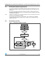
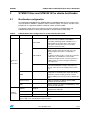
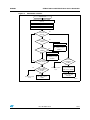
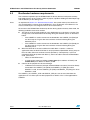
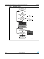
AN2606
Application note
STM32™ microcontroller
system memory boot mode
Introduction
The bootloader is stored in the internal boot ROM memory (system memory) of STM32
devices. It is programmed by ST during production. Its main task is to download the
application program to the internal Flash memory through one of the available serial
peripherals (USART, CAN, USB, etc.). A communication protocol is defined for each serial
interface, with a compatible command set and sequences.
The main features of the bootloader are the following:
●
It uses an embedded serial interface to download the code with a predefined
communication protocol
●
It transfers and updates the Flash memory code, the data, and the vector table sections
This application note presents the general concept of the bootloader. It describes the
supported peripherals and hardware requirements to be considered when using the
bootloader of any STM32 device currently in production. However the specifications of the
low-level communication protocol for each supported serial peripheral are documented in
separate documents:
●
For specifications of the USART protocol used in the bootloader please refer to
AN3155
●
For the specification of CAN protocol used in the bootloader please refer to AN3154
●
For the specification of DFU (USB Device) protocol used in the bootloader please refer
to AN3156
Related documents (available from www.st.com)
●
●
●
October 2010
STM32 datasheets:
–
low, medium and high-densitySTM32F101xx and STM32F103xx datasheets
–
low, medium and high-density STM32F100xx and STM32F102xx datasheets
–
STM32F105xx/107xx connectivity line datasheet
–
XL-density STM32F101xx and STM32F103xx datasheets
STM32 reference manuals:
–
STM32F101xx, STM32F102xx, STM32F103xx and STM32F105xx/107xx
reference manual (RM0008)
–
low, medium and high-density STM32F100xx value line reference manual
(RM0041)
STM32 Flash programming manuals
–
STM32F101xx, STM32F102xx, STM32F103xx and STM32F105xx/107xx Flash
programming manual (PM0042)
–
low, medium and high-density STM32F100xx value line Flash programming
manual (PM0063)
–
XL-density STM32F101xx and STM32F103xx programming manual (PM0068)
Doc ID 13801 Rev 9
1/27
www.st.com
Contents
AN2606
Contents
1
2
3
4
5
General bootloader description . . . . . . . . . . . . . . . . . . . . . . . . . . . . . . . . 6
1.1
Bootloader activation . . . . . . . . . . . . . . . . . . . . . . . . . . . . . . . . . . . . . . . . . 6
1.2
Exiting system memory boot mode . . . . . . . . . . . . . . . . . . . . . . . . . . . . . . 6
1.3
Bootloader identification . . . . . . . . . . . . . . . . . . . . . . . . . . . . . . . . . . . . . . . 6
STM32F101xx, STM32F102xx, STM32F103xx,
medium-density and high-density value line bootloader . . . . . . . . . . . 8
2.1
Bootloader configuration . . . . . . . . . . . . . . . . . . . . . . . . . . . . . . . . . . . . . . 8
2.2
Bootloader hardware requirements . . . . . . . . . . . . . . . . . . . . . . . . . . . . . . 9
2.3
Bootloader selection . . . . . . . . . . . . . . . . . . . . . . . . . . . . . . . . . . . . . . . . . . 9
2.4
Bootloader version . . . . . . . . . . . . . . . . . . . . . . . . . . . . . . . . . . . . . . . . . . 10
STM32F105xx and STM32F107xx device bootloader . . . . . . . . . . . . . . 11
3.1
Bootloader configuration . . . . . . . . . . . . . . . . . . . . . . . . . . . . . . . . . . . . . 11
3.2
Bootloader hardware requirements . . . . . . . . . . . . . . . . . . . . . . . . . . . . . 13
3.3
Bootloader selection . . . . . . . . . . . . . . . . . . . . . . . . . . . . . . . . . . . . . . . . . 14
3.4
Bootloader version . . . . . . . . . . . . . . . . . . . . . . . . . . . . . . . . . . . . . . . . . . 16
STM32F101xx and STM32F103xx XL-density devices bootloader . . . 17
4.1
Dual bank boot feature . . . . . . . . . . . . . . . . . . . . . . . . . . . . . . . . . . . . . . . 17
4.2
Bootloader configuration . . . . . . . . . . . . . . . . . . . . . . . . . . . . . . . . . . . . . 19
4.3
Bootloader hardware requirements . . . . . . . . . . . . . . . . . . . . . . . . . . . . . 20
4.4
Bootloader selection . . . . . . . . . . . . . . . . . . . . . . . . . . . . . . . . . . . . . . . . . 21
4.5
Bootloader version . . . . . . . . . . . . . . . . . . . . . . . . . . . . . . . . . . . . . . . . . . 23
Device-dependent bootloader parameters . . . . . . . . . . . . . . . . . . . . . . 24
Revision history . . . . . . . . . . . . . . . . . . . . . . . . . . . . . . . . . . . . . . . . . . . . . . . . . . . . 25
2/27
Doc ID 13801 Rev 9
AN2606
List of tables
List of tables
Table 1.
Table 2.
Table 3.
Table 4.
Table 5.
Table 6.
Table 7.
Table 8.
Table 9.
Table 10.
Table 11.
Boot pin configuration . . . . . . . . . . . . . . . . . . . . . . . . . . . . . . . . . . . . . . . . . . . . . . . . . . . . . . 6
Embedded bootloaders. . . . . . . . . . . . . . . . . . . . . . . . . . . . . . . . . . . . . . . . . . . . . . . . . . . . . 7
STM32F10xxx configuration in system memory boot mode . . . . . . . . . . . . . . . . . . . . . . . . . 8
STM32F10xxx bootloader versions evolution . . . . . . . . . . . . . . . . . . . . . . . . . . . . . . . . . . . 10
STM32F105xx/107xx configuration in system memory boot mode . . . . . . . . . . . . . . . . . . 11
STM32F105xx and STM32F107xx bootloader versions evolution . . . . . . . . . . . . . . . . . . . 16
Boot pin and BFB2 bit configuration . . . . . . . . . . . . . . . . . . . . . . . . . . . . . . . . . . . . . . . . . . 18
STM32F10xxx XL-density configuration in system memory boot mode . . . . . . . . . . . . . . . 19
Evolution of the XL-density bootloader versions. . . . . . . . . . . . . . . . . . . . . . . . . . . . . . . . . 23
Bootloader device dependant parameters . . . . . . . . . . . . . . . . . . . . . . . . . . . . . . . . . . . . . 24
Document revision history . . . . . . . . . . . . . . . . . . . . . . . . . . . . . . . . . . . . . . . . . . . . . . . . . 25
Doc ID 13801 Rev 9
3/27
List of figures
AN2606
List of figures
Figure 1.
Figure 2.
Figure 3.
4/27
Bootloader for STM32 with USART1 . . . . . . . . . . . . . . . . . . . . . . . . . . . . . . . . . . . . . . . . . . 9
Bootloader selection . . . . . . . . . . . . . . . . . . . . . . . . . . . . . . . . . . . . . . . . . . . . . . . . . . . . . . 15
Bootloader selection . . . . . . . . . . . . . . . . . . . . . . . . . . . . . . . . . . . . . . . . . . . . . . . . . . . . . . 22
Doc ID 13801 Rev 9
AN2606
Glossary
Low-density devices are STM32F101xx, STM32F102xx and STM32F103xx
microcontrollers where the Flash memory density ranges between 16 and 32 Kbytes.
Medium-density devices are STM32F101xx, STM32F102xx and STM32F103xx
microcontrollers where the Flash memory density ranges between 64 and 128 Kbytes.
High-density devices are STM32F101xx and STM32F103xx microcontrollers where the
Flash memory density ranges between 256 and 512 Kbytes.
Connectivity line devices are STM32F105xx and STM32F107xx microcontrollers.
Low-density value line devices are STM32F100xx microcontrollers where the Flash
memory density ranges between 16 and 32 Kbytes.
Medium-density value line devices are STM32F100xx microcontrollers where the Flash
memory density ranges between 64 and 128 Kbytes.
High-density value line devices are STM32F100xx microcontrollers where the Flash
memory density ranges between 256 and 5128 Kbytes.
XL-density devices are STM32F101xx and STM32F103xx microcontrollers where the
Flash memory density ranges between 768 Kbytes and 1 Mbyte.
Doc ID 13801 Rev 9
5/27
General bootloader description
AN2606
1
General bootloader description
1.1
Bootloader activation
The bootloader is automatically activated by configuring the BOOT0 and BOOT1 pins in the
specific “System memory” configuration (see Table 1) and then by applying a reset.
Depending on the used pin configuration, the Flash memory, system memory or SRAM is
selected as the boot space, as shown in Table 1 below.
Table 1.
Boot pin configuration
Boot mode selection pins
Boot mode
BOOT1
Aliasing
BOOT0
X
0
User Flash memory User Flash memory is selected as the boot space
0
1
System memory
System memory is selected as the boot space
1
1
Embedded SRAM
Embedded SRAM is selected as the boot space
Table 1 shows that the STM32 microcontrollers enter the System memory boot mode if the
BOOT pins are configured as follows:
●
BOOT0 = 1
●
BOOT1 = 0
The values on the BOOT pins are latched on the fourth rising edge of SYSCLK after a reset.
1.2
Exiting system memory boot mode
System memory boot mode must be exited in order to start execution of the application
program. This can be done by applying a hardware reset. During reset, the BOOT pins
(BOOT0 and BOOT1) must be set at the proper levels to select the desired boot mode (see
Table 1). Following the reset, the CPU starts code execution from the boot memory located
at the bottom of the memory address space starting from 0x0000 0000.
1.3
Bootloader identification
Depending on the used STM32 device, the bootloader may support one or more embedded
serial peripherals used to download the code to the internal Flash memory. The bootloader
identifier (ID) provides information about the supported serial peripherals.
For a given STM32 device, the bootloader is identified by means of the:
6/27
Doc ID 13801 Rev 9
AN2606
General bootloader description
1.
Bootloader (protocol) version: version of the serial peripheral (USART, CAN, USB,
etc.) communication protocol used in the bootloader. This version can be retrieved
using the bootloader Get Version command.
2.
Bootloader identifier (ID): version of the STM32 device bootloader, coded on one byte
in the 0xXY format, where:
–
X specifies the embedded serial peripheral(s) used by the device bootloader:
X = 1: only one USART is used
X = 2: two USARTs are used
X = 3: two USARTs, one CAN and DFU are used
–
Y specifies the device bootloader version
Let us take the example of a bootloader ID equal to 0x10. This means that it is the
first version of the device bootloader that uses only one USART.
The bootloader ID is programmed in the last two bytes of the device system
memory and can be read by using the bootloader “Read memory” command or by
direct access to the system memory via JTAG/SWD.
The table below provides identification information about the bootloader embedded in
STM32 devices.
Table 2.
Embedded bootloaders
Bootloader ID
Device
Supported serial peripherals
ID
Memory location
Bootloader
(protocol)
version
Low-density
USART1
NA
NA
USART (V2.2)
Medium-density
USART1
NA
NA
USART (V2.2)
High-density
USART1
NA
NA
USART (V2.2)
Connectivity line
USART1 / USART2 (remapped) /
CAN2 (remapped) / DFU (USB
Device)
NA
NA
USART
(V2.2(1))
CAN (V2.0)
DFU(V2.0)
Medium-density
value line
USART1
V1.0
0x1FFFF7D6
USART (V2.2)
High-density
value line
USART1
V1.0
0x1FFFF7D6
USART (V2.2)
XL-density
USART1/USART2 (remapped)
V2.1
0x1FFFF7D6
USART (V3.0)
1. For connectivity line devices, the USART bootloader returns V2.0 instead of V2.2 for the protocol version.
For more details please refer to the "STM32F105xx and STM32F107xx revision Z" errata sheet available
from www.st.com.
Doc ID 13801 Rev 9
7/27
STM32F101xx, STM32F102xx, STM32F103xx, medium-density and high-density value line boot-
2
STM32F101xx, STM32F102xx, STM32F103xx,
medium-density and high-density value line
bootloader
Throughout this section STM32F10xxx will be used to refer to low-density, medium-density,
high-density STM32F101xx and STM32F103xx devices, to low- and medium-density
STM32F102xx devices and to medium and high-density value line devices.
2.1
Bootloader configuration
The bootloader embedded in STM32F10xxx devices supports only one interface: the
USART1.
The following table shows the required STM32F10xxx hardware resources used by the
bootloader in System memory boot mode.
Table 3.
STM32F10xxx configuration in system memory boot mode
Feature/Peripheral
8/27
Comment
Clock source
HSI enabled The system clock is equal to 24 MHz using the PLL
USART1_RX pin
Input
PA10 pin: USART1 receives
USART1_TX pin
Output
PA9 pin: USART1 transmits
SysTick timer
Enabled
Used to automatically detect the serial baud rate from the host.
USART1
Enabled
Once initialized the USART1 configuration is: 8-bits, even parity
and 1 Stop bit
RAM
-
512 bytes starting from address 0x2000 0000 are used by the
bootloader firmware
System memory
-
2 Kbytes starting from address 0x1FFF F000, contain the
bootloader firmware
-
The independent watchdog (IWDG) prescaler is configured to its
maximum value and is periodically refreshed to prevent
watchdog reset (in case the hardware IWDG option was
previously enabled by the user)
IWDG
Note:
State
1
The system clock is derived from the embedded internal high-speed RC, no external quartz
is required for the bootloader code
2
After downloading the application binary, if you choose to execute the Go command, the
peripheral registers used by the bootloader (shown in the above table) are not initialized to
their default reset values before jumping to the user application. They should be
reconfigured in the user application if they are used. So, if the IWDG is being used in the
application, the IWDG prescaler value has to be adapted to meet the requirements of the
application (since the prescaler was set to its maximum value by the bootloader).
Doc ID 13801 Rev 9
AN2606STM32F101xx, STM32F102xx, STM32F103xx, medium-density and high-density value line
2.2
Bootloader hardware requirements
The hardware required to put the STM32 into System memory boot mode consists of any
circuitry, switch or jumper, capable of holding the BOOT0 pin high and the BOOT1 pin low
during reset.
To connect to the STM32 during System memory boot mode, an RS232 serial interface
(example, ST3232 RS232 transceiver) has to be directly linked to the USART1_RX (PA10)
and USART1_TX (PA9) pins.
Note:
USART1_CK, USART1_CTS and USART1_RTS pins are not used, therefore user can use
these pins for other peripherals or GPIOs.
For more details about hardware recommendations, refer to application note AN2586:
“STM32 hardware development: getting started”, available from the STMicroelectronics
website: www.st.com
2.3
Bootloader selection
Figure 1.
Bootloader for STM32 with USART1
3YSTEMRESET
$ISABLEALLINTERRUPTSOURCES
#ONFIGUREINTERNAL2#MODE
7AITFOR&H
FROMHOST
!UTOBAUDRATESEQUENCE
SEND!#+BYTEDISABLE
UNUSEDPERIPHERALS
7AITFORA
COMMAND
#OMMAND
RECEIVED
'/CMD
'%4CMD
'%4CMD
ROUTINE
2$CMD
ROUTINE
OPTIONAL
LOADROUTINES
INTO2!-
'/CMD
ROUTINE
*0TO?!DDRESS
AIB
Doc ID 13801 Rev 9
9/27
STM32F101xx, STM32F102xx, STM32F103xx, medium-density and high-density value line bootOnce System memory boot mode is entered and the microcontroller has been configured as
described above, the bootloader code begins to scan the USART1_RX line pin, waiting to
receive the 0x7F data frame: one start bit, 0x7F data bits, even parity bit and one stop bit.
The duration of this data frame is measured using the Systick timer. The count value of the
timer is then used to calculate the corresponding baud rate factor with respect to the current
system clock.
Next, the code initializes the serial interface accordingly. Using this calculated baud rate, an
acknowledge byte (0x79) is returned to the host, which signals that the STM32F10xxx is
ready to receive user commands.
2.4
Bootloader version
The Table 4 lists the bootloader versions evolution of the STM32F10xxx devices.
Table 4.
STM32F10xxx bootloader versions evolution
Bootloader version number
10/27
Description
V2.0
Initial bootloader version.
V2.1
– Update Go Command to initialize the main stack pointer
– Update Go command to return NACK when jump address is in
the Option byte area or System memory area
– Update Get ID command to return the device ID on two bytes
– Update the bootloader version to V2.1
V2.2
– Update Read Memory, Write Memory and Go commands to
deny access with a NACK response to the first 0x200 bytes of
RAM memory used by the bootloader
– Update Readout Unprotect command to initialize the whole RAM
content to 0x0 before ROP disable operation
Doc ID 13801 Rev 9
AN2606
STM32F105xx and STM32F107xx device bootloader
3
STM32F105xx and STM32F107xx device bootloader
3.1
Bootloader configuration
The bootloader embedded in the STM32F105xx and STM32F107xx devices supports four
serial peripherals: USART1, USART2, CAN2, and DFU (USB). This means that four serial
peripherals are supported: USART1, USART2, CAN2 and DFU (USB).
The following table shows the hardware resources required by STM32F105xx and
STM32F107xx devices used by the bootloader in System memory boot mode.
Table 5.
Bootloader
STM32F105xx/107xx configuration in system memory boot mode
Feature/Peripheral
State
HSI enabled
The system clock frequency is 24 MHz using the PLL.
This is used only for USART1 and USART2
bootloaders and during CAN2, USB detection for
CAN and DFU bootloaders (Once CAN or DFU
bootloader is selected, the clock source will be
derived from external crystal).
HSE enabled
The external clock is mandatory only for DFU and
CAN bootloaders and it must provide one of the
following frequencies: 8 MHz, 14.7456 MHz or
25 MHz.
For CAN Bootloader, the PLL is used only to generate
48 MHz when 14.7456 MHz is used as HSE.
For DFU Bootloader, the PLL is used to generate a
48 MHz system clock from all supported external
clock frequencies.
-
The clock security system (CSS) interrupt is enabled
for the CAN and DFU bootloaders. Any failure (or
removal) of the external clock will generate system
reset.
IWDG
-
The independent watchdog (IWDG) prescaler is
configured to its maximum value and is periodically
refreshed to prevent watchdog reset (in case the
hardware IWDG option was previously enabled by the
user).
System memory
-
18 Kbytes starting from address 0x1FFF B000,
contain the bootloader firmware
RAM
-
4 Kbytes starting from address 0x2000 0000 are used
by the bootloader firmware.
USART1
Enabled
Once initialized the USART1 configuration is: 8-bits,
even parity and 1 Stop bit
USART1_RX pin
Input
PA10 pin: USART1 receive
USART1_TX pin
Output
PA9 pin: USART1 transmit
RCC
Common to
all
bootloaders
USART1
bootloader
Comment
USART2_RX (PD6), CAN2_RX (PB5), OTG_FS_DM (PA11) and OTG_FS_DP (PA12) pins must be
kept at a high or low level during the detection phase.
Doc ID 13801 Rev 9
11/27
STM32F105xx and STM32F107xx device bootloader
Table 5.
Bootloader
STM32F105xx/107xx configuration in system memory boot mode (continued)
Feature/Peripheral
USART1 and
USART2
SysTick timer
bootloaders
USART2
bootloader
AN2606
State
Comment
Enabled
Used to automatically detect the serial baud rate from
the host for USARTx bootloader.
USART2
Enabled
Once initialized the USART2 configuration is: 8-bits,
even parity and 1 Stop bit. The USART2 uses its
remapped pins.
USART2_RX pin
Input
PD6 pin: USART2 receive (remapped pin)
USART2_TX pin
Output
PD5 pin: USART2 transmit (remapped pin)
USART1_RX (PA10), CAN2_RX (PB5), OTG_FS_DM (PA11) and OTG_FS_DP (PA12) pins must
be kept at a high or low level during the detection phase.
CAN2
Enabled
Once initialized the CAN2 configuration is: Baudrate
125 kbps, 11-bit identifier.
Note: CAN1 is clocked during the CAN bootloader
execution because in STM32F105xx and
STM32F107xx devices, CAN1 manages the
communication between CAN2 and SRAM.
CAN2_RX pin
Input
PB5 pin: CAN2 receives (remapped pin)
CAN2_TX pin
Output
PB6 pin: CAN2 transmits (remapped pin)
CAN2
bootloader
USART1_RX (PA10), USART2_RX (PD6), OTG_FS_DM (PA11) and OTG_FS_DP (PA12) pins
must be kept at a high or low level during the detection phase.
USB OTG FS
DFU
bootloader
Enabled
USB OTG FS configured in Forced device mode
OTG_FS_VBUS pin Input or alternate
PA9: Power supply voltage line
function, automatically
OTG_FS_DM pin
PA11: USB Send-Receive data line
controlled by the USB
OTG FS controller
OTG_FS_DP pin
PA12: USB Send-Receive data line
Interrupts
Enabled
USB_OTG_FS interrupt vector is enabled and used
for USB DFU communication.
USART1_RX (PA10), USART2_RX (PD6) and CAN2_RX (PB5) pins must be kept at a high or low
level during the detection phase.
The system clock is derived from the embedded internal high-speed RC for USARTx
bootloader. This internal clock is used also for DFU and CAN bootloaders but only for the
selection phase. An external clock (8 MHz, 14.7456 MHz or 25 MHz.) is required for DFU
and CAN bootloader execution after the selection phase.
After downloading the application binary, if you choose to execute the Go command, all
peripheral registers used by the bootloader (shown in the above table) will be initialized to
their default reset values before jumping to the user application.
If the user application uses the IWDG, the IWDG prescaler value has to be adapted to meet
the requirements of the application (since the prescaler was set to its maximum value by the
bootloader).
12/27
Doc ID 13801 Rev 9
AN2606
3.2
STM32F105xx and STM32F107xx device bootloader
Bootloader hardware requirements
The hardware required to put the STM32F105xx and STM32F107xx into System memory
boot mode consists of any circuitry, switch or jumper, capable of holding the BOOT0 pin high
and the BOOT1 pin low during reset.
To connect to the STM32F105xx and STM32F107xx during System memory boot mode, the
following conditions have to be verified:
●
●
The RX pins of the unused peripherals in this bootloader have to be kept at a known
(low or high) level, and should not be left floating during the detection phase as
described below:
–
If USART1 is used to connect to the bootloader: the USART2_RX (PD6),
CAN2_RX (PB5), OTG_FS_DM (PA11) and OTG_FS_DP (PA12) pins have to be
kept at a high or low level and must not be left floating during the detection phase.
–
If USART2 is used to connect to the bootloader: the USART1_RX (PA10),
CAN2_RX (PB5), OTG_FS_DM (PA11) and OTG_FS_DP (PA12) pins have to be
kept at a high or low level and must not be left floating during the detection phase.
–
If CAN2 is used to connect to the bootloader: the USART1_RX (PA10),
USART2_RX (PD6), OTG_FS_DM (PA11) and OTG_FS_DP (PA12) pins have to
be kept at a high or low level and must not be left floating during the detection
phase.
–
If DFU is used to connect to the bootloader: the USART1_RX (PA10),
USART2_RX (PD6) and CAN2_RX (PB5) pins have to be kept at a high or low
level and must not be left floating during the detection phase.
Connect to the peripheral to be used through:
–
an RS232 serial interface (example, ST3232 RS232 transceiver) has to be directly
connected to the USART1_RX (PA10) and USART1_TX (PA9) pins when
USART1 is used, or to the USART2_RX (PD6) and USART2_TX (PD5) pins when
USART2 is used
–
a CAN interface (CAN transceiver) has to be directly connected to the CAN2_RX
(PB5) and CAN2_TX (PB6) pins
–
a certified USB cable has to be connected to the microcontroller (optionally an
ESD protection circuitry can be used)
The USART1_CK, USART1_CTS and USART1_RTS pins are not used, therefore the
application can use these pins for other peripherals or GPIOs. The same note is applicable
for USART2.
Once the USB Device is enabled, all its related pins are dedicated to USB communication
only, and cannot be used for other application purposes.
The user can control the BOOT0 and Reset pins from a PC serial applet using the RS232
serial interface which controls BOOT0 through the CTS line and Reset through the DCD
line. The user must use a full null modem cable. The necessary hardware to implement for
this control exists in the STM3210C-EVAL board. For more details about this, refer to
document: “STM3210C-EVAL board user manual”, available from the STMicroelectronics
website: www.st.com.
Doc ID 13801 Rev 9
13/27
STM32F105xx and STM32F107xx device bootloader
3.3
AN2606
Bootloader selection
The STM32F105xx and STM32F107xx embedded bootloader supports four peripherals
interfaces: USART1, USART2, CAN2 and DFU (USB). Any one of these peripheral
interfaces can be used to communicate with the bootloader and download the application
code to the internal Flash.
The embedded bootloader firmware is able to auto-detect the peripheral interface to be
used. In an infinite loop, it detects any communication on the supported bootloader
interfaces.
Note:
The RX pins of the unused peripherals in this bootloader have to be maintained at a known
(low or high) level and should not be left floating during the detection phase as described
below:
●
If USART1 is used to connect to the bootloader: the USART2_RX (PD6), CAN2_RX
(PB5), OTG_FS_DM (PA11) and OTG_FS_DP (PA12) pins have to be kept at a high or
low level and must not be left floating during the detection phase.
●
If USART2 is used to connect to the bootloader: the USART1_RX (PA10), CAN2_RX
(PB5), OTG_FS_DM (PA11) and OTG_FS_DP (PA12) pins have to be kept at a high or
low level and must not be left floating during the detection phase.
●
If CAN2 is used to connect to the bootloader: USART1_RX (PA10), USART2_RX
(PD6), OTG_FS_DM (PA11) and OTG_FS_DP (PA12) pins have to be kept at a high or
low level and must not be left floating during the detection phase.
●
If DFU is used to connect to the bootloader: the USART1_RX (PA10), USART2_RX
(PD6) and CAN2_RX (PB5) pins have to be kept at a high or low level and must not be
left floating during the detection phase.
To use the USART bootloader on USART1 or USART2, connect the serial cable to the
desired interface. Once the bootloader detects the data byte 0x7F on this interface, the
bootloader firmware executes the auto-baud rate sequence and then enters a loop, waiting
for any USART bootloader command.
To use the CAN2 interface, connect the CAN cable to CAN2. Once the bootloader detects a
frame on the CAN2_RX pin (PB5), the bootloader firmware enters a CAN loop and starts to
check the external clock frequency value, if the HSE is 8 MHz, 14.7456 MHz or 25 MHz
CAN bootloader firmware enters an infinite loop and waits until it receives a message,
otherwise a system reset is generated.
If a USB cable is plugged into the microcontroller’s USB interface at any time during the
bootloader firmware selection sequence, the bootloader then enters the DFU bootloader
loop waiting for any DFU bootloader command.
To use the USART or the CAN bootloader, it is mandatory that no USB cable is connected to
the USB peripheral during the selection phase. Once the USART or CAN bootloader is
selected, the user can plug a USB cable without impacting the selected bootloader
execution except commands which generate a system reset.
Once one interface is selected for the bootloader, all other interfaces are disabled.
The figure below shows the bootloader detection mechanism. More details are provided in
the sections corresponding to each peripheral bootloader.
14/27
Doc ID 13801 Rev 9
AN2606
STM32F105xx and STM32F107xx device bootloader
Figure 2.
Bootloader selection
System reset
System init (clock, GPIOs, IWDG,
SysTick)
Configure CAN2
Configure USB
Yes
USB cable
detected
No
Yes
0x7F received on
USART1
Configure USART1
No
Yes
0x7F received on
USART2
Execute
BL_USART_Loop for
USART1
Configure USART2
No
Execute
BL_USART_Loop for
USART2
No
No
Frame detected on
CAN2_RX pin
Yes
Yes
No
HSE = 8 MHz,
14.7456 MHz or
25 MHz
Yes
Generate system
reset
Execute
BL_CAN_Loop for
CAN2
HSE = 8 MHz,
14.7456 MHz or
25 MHz
Generate system
reset
Reconfigure system
clock to 48 MHz and
USB clock to 48 MHz
Execute DFU bootloader using USB
interrupts
ai17514
Doc ID 13801 Rev 9
15/27
STM32F105xx and STM32F107xx device bootloader
3.4
AN2606
Bootloader version
The table below lists the bootloader versions and the changes between versions V1.0 and
V2.0. of the STM32F105xx and STM32F107xx devices
Table 6.
STM32F105xx and STM32F107xx bootloader versions evolution
Bootloader version
number
16/27
Description
V1.0
Initial bootloader version.
V2.0
– Bootloader detection mechanism updated to fix the issue when GPIOs of
unused peripherals in this bootloader are connected to low level or left
floating during the detection phase.
For more details please refer to limitation 2.12 “Boot loader unavailability on
STM32F105xx and STM32F107xx devices with a date code below 937” as
described in Revision 2 of the “STM32F105xx and STM32F107xx revision
Z” errata sheet available from www.st.com
– Vector table set to 0x1FFF B000 instead of 0x0000 0000
– Go command updated (for all bootloaders): USART1, USART2, CAN2,
GPIOA, GPIOB, GPIOD and SysTick peripheral registers are set to their
default reset values
– DFU bootloader: USB pending interrupt cleared before executing the Leave
DFU command
– DFU subprotocol version changed from V1.0 to V1.2
– Bootloader version updated to V2.0
Doc ID 13801 Rev 9
AN2606
STM32F101xx and STM32F103xx XL-density devices bootloader
4
STM32F101xx and STM32F103xx XL-density devices
bootloader
Throughout this section STM32F10xxx XL-density is used to refer to XL-density
STM32F101xx and STM32F103xx devices.
4.1
Dual bank boot feature
For STM32F101xx and STM32F103xx XL-density devices (these devices have two Flash
memory banks: Bank 1 and Bank 2), an additional boot mechanism is available which allows
booting from Bank 2 or Bank 1 (depending on the BFB2 bit status (bit 19 in the user option
bytes @ 0x1FFFF800)).
1.
2.
Note:
When the BFB2 bit is reset, and the boot pins are configured to boot from the Flash
memory (BOOT0 = 0 and BOOT1 = x) then, after reset, the device boots from the
System memory and executes the embedded bootloader code which implements the
dual bank Boot mode:
a)
First, the code checks Bank 2. If it contains a valid code (see Note: 1 below), it
jumps to application located in Bank 2 and leaves the Bootloader.
b)
If the Bank 2 code is not valid, it checks Bank 1 code. If it is valid (see “note”
below), it jumps to the application located in Bank 1.
c)
If both Bank 2 and Bank 1 do not contain valid code (see “note” below), the normal
Bootloader operations are executed as described in the following sections (no
jump to Flash banks is executed). Refer to Figure 3: Bootloader selection for more
details.
When the bit BFB2 is set (default state), the dual bank boot mechanism is not
performed.
1
The code is considered as valid when the first data (at the bank start address, which should
be the stack pointer) points to a valid address into the internal SRAM memory (stack top
address). If the first address points to any other location (out of the internal SRAM) the code
is considered not valid.
2
A dual bank Boot mode example (FLASH\Dual_Boot) is provided within the STM32F10x
Standard Peripheral Library available on www.st.com.
Doc ID 13801 Rev 9
17/27
STM32F101xx and STM32F103xx XL-density devices bootloader
AN2606
For the STM32F101xx and STM32F103xx XL-density devices, the Flash memory, system
memory or SRAM is selected as the boot space, as shown in Table 7 below.
Table 7.
Boot pin and BFB2 bit configuration
Boot mode
selection pins
BFB2
bit
1
0
Boot mode
Aliasing
BOOT1
BOOT0
X
0
User Flash memory
User Flash memory is selected as the boot
space
0
1
System memory
System memory is selected as the boot space
1
1
Embedded SRAM
Embedded SRAM is selected as the boot
space
X
0
System memory
System memory is selected as the boot space
then dual bank mechanism is executed
0
1
System memory
System memory is selected as the boot space
then dual bank mechanism is executed
1
1
Embedded SRAM
Embedded SRAM is selected as the boot
space
Table 7 shows that the XL-density devices enter the System memory boot mode in two
cases:
Note:
1.
If the BOOT pins are configured as follows: BOOT0 = 1 and BOOT1 = 0
2.
Or if:
a)
the BFB2 bit is reset and
b)
boot pins are configured as follows: BOOT0 = 0 and BOOT1 = x
When conditions a, b, and c below are fulfilled, it is equivalent to configuring boot pins for
system memory boot (BOOT0 = 1 and BOOT1 = 0). In this case normal Bootloader
operations are executed.
a)
BFB2 bit is reset
b)
Both banks don’t contain valid code
c)
Boot pins configured as follows: BOOT0 = 0 and BOOT1 = x
When the BFB2 bit is cleared, and Bank 2 and/or Bank 1 contain valid user application
code, the Dual Bank Boot is always performed (bootloader always jumps to the user code
and never continues normal operations).
Consequently, if you have cleared the BFB2 bit (to boot from Bank 2) then, to be able to
execute the Bootloader code, you have to:
- either, set the BFB2 bit to 1
- or, program the content of address 0x0808 0000 (base address of Bank2) and 0x0800
0000 (base address of Bank1) to 0x0
18/27
Doc ID 13801 Rev 9
AN2606
STM32F101xx and STM32F103xx XL-density devices bootloader
4.2
Bootloader configuration
The bootloader embedded in STM32F10xxx XL-density supports two serial interfaces:
USART1 and USART2.
The following table shows the required hardware resources of STM32F10xxx XL-density
devices used by the bootloader in system memory boot mode.
Table 8.
STM32F10xxx XL-density configuration in system memory boot mode
Feature/peripheral
Comment
Clock source
HSI enabled
The system clock is equal to 24 MHz using the PLL
USART1_RX pin
Input
PA10 pin: USART1 receives
USART1_TX pin
Output
PA9 pin: USART1 transmits
USART2_RX pin
Input
PD6 pin: USART2 receives (remapped pins)
USART2_TX pin
Output
PD5 pin: USART2 transmits (remapped pins)
SysTick timer
Enabled
Used to automatically detect the serial baud rate from the host
USART1
Enabled
USART2
Enabled
Once initialized the USART1/USART2 configuration is: 8-bits,
even parity and 1 Stop bit.
RAM
-
2 Kbytes starting from address 0x2000 0000 are used by the
bootloader firmware
System memory
-
6 Kbytes starting from address 0x1FFF E000, contain the
bootloader firmware
-
The independent watchdog (IWDG) prescaler is configured to
its maximum value and is periodically refreshed to prevent
watchdog reset (in case the hardware IWDG option was
previously enabled by the user)
IWDG
Note:
State
1
The system clock is derived from the embedded internal high-speed RC, no external quartz
is required for the bootloader code
2
After downloading the application binary, if you choose to execute the Go command, all
peripheral registers used by the bootloader (shown in Table 8) are initialized to their default
reset values before jumping to the user application.
If the user application uses the IWDG, the IWDG prescaler value has to be adapted to meet
the requirements of the application (since the prescaler was set to its maximum value by the
bootloader).
Doc ID 13801 Rev 9
19/27
STM32F101xx and STM32F103xx XL-density devices bootloader
4.3
AN2606
Bootloader hardware requirements
The hardware required to put the STM32F10xx XL-density devices into System memory
boot mode consists of any circuitry, switch or jumper, capable of holding the BOOT0 pin high
and the BOOT1 pin low during reset.
Note:
As explained in Section 4.1: Dual bank boot feature, the system memory boot mode can
also be executed by software when the BFB2 bit is reset, both banks start addresses are
erased, and boot pins are configured to boot from Flash memory.
To connect to the STM32F10xx XL-density devices during System memory boot mode, the
following conditions have to be verified:
●
●
●
The RX pin of the unused peripheral in this bootloader has to be kept at a known (low
or high) level, and should not be left floating during the detection phase as described
below:
–
If the USART1 is used to connect to the bootloader: the USART2_RX (PD6) pin
has to be kept at a high or low level and must not be left floating during the
detection phase.
–
If the USART2 is used to connect to the bootloader: the USART1_RX (PA10) pin
has to be kept at a high or low level and must not be left floating during the
detection phase.
When the BFB2 bit is cleared, and Bank 2 and/or Bank 1 contain a valid user
application code, the Dual Bank Boot is always performed (bootloader always jumps to
the user code and never continues normal operations). Consequently, if you have
cleared the BFB2 bit (to boot from Bank 2), then to be able to execute the Bootloader
code, you have to:
–
either, set the BFB2 bit to 1
–
or, program the content of address 0x0808 0000 (base address of Bank2) and
0x0800 0000 (base address of Bank1) to 0x0
Connect to the peripheral to be used through:
–
an RS232 serial interface (example, ST3232 RS232 transceiver) has to be directly
connected to the USART1_RX (PA10) and USART1_TX (PA9) pins when
USART1 is used, or to the USART2_RX (PD6) and USART2_TX (PD5) pins when
USART2 is used
The USART1_CK, USART1_CTS and USART1_RTS pins are not used, therefore the
application can use these pins for other peripherals or GPIOs. This is also applicable for
USART2.
20/27
Doc ID 13801 Rev 9
AN2606
4.4
STM32F101xx and STM32F103xx XL-density devices bootloader
Bootloader selection
The STM32F10xx XL-density embedded Bootloader supports two peripheral interfaces:
USART1 and USART2. Any one of these peripheral interfaces can be used to communicate
with the bootloader and download the application code to the internal Flash.
The embedded Bootloader firmware is able to auto-detect the peripheral interface to be
used. In an infinite loop, it detects any communication on the supported bootloader
interfaces.
Note:
The RX pin of the unused peripheral in this bootloader has to be maintained at a known (low
or high) level and should not be left floating during the detection phase as described below:
●
If USART1 is used to connect to the bootloader: the USART2_RX (PD6) pin has to be
kept at a high or low level and must not be left floating during the detection phase.
●
If USART2 is used to connect to the bootloader: the USART1_RX (PA10) pin has to be
kept at a high or low level and must not be left floating during the detection phase.
To use the USART bootloader on USART1 or USART2, connect the serial cable to the
desired interface. Once the bootloader detects the data byte 0x7F on this interface, the
bootloader firmware executes the auto-baudrate sequence and then enters a loop, waiting
for any USART bootloader command.
Once one interface is selected for the bootloader, the other interface is disabled.
Figure 3 shows the bootloader detection mechanism. More details are provided in the
sections corresponding to each peripheral bootloader.
Doc ID 13801 Rev 9
21/27
STM32F101xx and STM32F103xx XL-density devices bootloader
Figure 3.
AN2606
Bootloader selection
System Reset
BFB2 bit is reset
(BFB2 = 0)
NO
YES
YES
If value @ 0x0808 0000 is
within int. SRAM address
Jump to user code in
Bank 2
NO
YES
If value @ 0x0800 0000 is
within int. SRAM address
NO
Jump to user code in
Bank 1
Continue normal Bootloader
execution
Disable all interrupt sources
System init (clock, GPIOs, IWDG,
SysTick)
0x7f received
on USART1
YES
NO
Configure USART1
NO
0x7f received
on USART2
YES
Execute BL_USART_Loop
for USART1
Configure USART2
Execute BL_USART_Loop
for USART2
AI
22/27
Doc ID 13801 Rev 9
AN2606
4.5
STM32F101xx and STM32F103xx XL-density devices bootloader
Bootloader version
Table 9 lists the bootloader versions for the STM32F101xx and STM32F103xx XL-density
devices.
Table 9.
Evolution of the XL-density bootloader versions
Bootloader version
number
V2.1
Description
Initial bootloader version
Doc ID 13801 Rev 9
23/27
Device-dependent bootloader parameters
5
AN2606
Device-dependent bootloader parameters
The bootloader protocol’s command set and sequences for each serial peripheral (USART,
CAN and USB) are the same for all STM32 devices. Some parameters, however, are
device-dependent. For a few commands, the value of some parameters may depend on the
device used. These parameters are listed below:
●
PID (product ID), which changes with the device
●
Valid memory addresses (RAM, Flash memory, system memory, option byte area)
accepted by the bootloader when the Read Memory, Go and Write Memory commands
are accepted.
●
Size of the Flash memory sector used when executing the Write Protect command.
The table below shows the values of these parameters for each STM32 device bootloader in
production.
Table 10.
Device
Bootloader device dependant parameters
Product
(device) ID
RAM memory
Flash memory Flash sector size
Option byte
area
System
memory
Low-density
0x412
0x20000200 up 0x08000000 up 4 Kbytes (4 pages 0x1FFFF800 - 0x1FFFF000 to 0x20002800 to 0x08008000 of 1 Kbyte each)
0x1FFFF80F 0x1FFFF800
Mediumdensity
0x410
0x20000200 up 0x08000000 up 4 Kbytes (4 pages 0x1FFFF800 - 0x1FFFF000 to 0x20005000 to 0x08020000 of 1 Kbyte each)
0x1FFFF80F 0x1FFFF800
High-density 0x414
0x20000200 up 0x08000000 up 4 Kbytes (2 pages 0x1FFFF800 - 0x1FFFF000 to 0x20010000 to 0x08080000 of 2 Kbytes each) 0x1FFFF80F 0x1FFFF800
Connectivity
0x418
line
0x20001000 up 0x08000000 up 4 Kbytes (2 pages 0x1FFFF800 - 0x1FFFB000
to 0x20010000 to 0x08040000 of 2 Kbytes each) 0x1FFFF80F - 0x1FFFF800
Mediumdensity
value line
0x420
0x20000200 up 0x08000000 up 4 Kbytes (4 pages 0x1FFFF800 - 0x1FFFF000 to 0x20002000 to 0x08020000 of 1 Kbyte each)
0x1FFFF80F 0x1FFFF800
High-density
0x428
value line
0x20000200 up 0x08000000 up 4 Kbytes (2 pages 0x1FFFF800 - 0x1FFFF000 to 0x20008000 to 0x08080000 of 2 Kbytes each) 0x1FFFF80F 0x1FFFF800
XL-density
0x20000800 up 0x08000000 up 4 Kbytes (2 pages 0x1FFFF800 - 0x1FFFE000
to 0x20018000 to 0x08100000 of 2 Kbytes each) 0x1FFFF80F - 0x1FFFF800
24/27
0x430
Doc ID 13801 Rev 9
AN2606
Revision history
Revision history
Table 11.
Document revision history
Date
Revision
22-Oct-2007
1
Initial release.
2
All STM32 in production (rev. B and rev. Z) include the bootloader
described in this application note.
Modified: Section 1.1: Bootloader activation and Section 1.4:
Bootloader code sequence.
Added: Section 1.3: Hardware requirements, Section 1.5: Choosing
the USART baud rate, Section 1.6: Using the bootloader and
Section 1.2: Exiting system memory boot mode.
Note 2 linked to Get, Get Version & Read Protection Status and Get
ID commands in Table 3: Bootloader commands, Note 3 added.
Notion of “permanent” (Permanent Write Unprotect/Readout
Protect/Unprotect) removed from document. Small text changes.
Bootloader version upgraded to 2.0.
3
Small text changes. RAM and System memory added to Table 3:
STM32F10xxx configuration in system memory boot mode.
Section 1.6: Using the bootloader on page 8 removed.
Erase modified, Note 3 modified and Note 1 added in Table 3:
Bootloader commands on page 9.
Byte 3: on page 11 modified.
Byte 2: on page 13 modified.
Byte 2:, Bytes 3-4: and Byte 5: on page 15 modified, Note 3
modified.
Byte 8: on page 18 modified.
Notes added to Section 2.5: Go command on page 18.
Figure 11: Go command: device side on page 20 modified.
Note added in Section 2.6: Write Memory command on page 21.
Byte 8: on page 24 modified.
Figure 14: Erase Memory command: host side and Figure 15: Erase
Memory command: device side modified.
Byte 3: on page 26 modified.
Table 3: Bootloader commands on page 9.
Note modified and note added in Section 2.8: Write Protect
command on page 27.
Figure 16: Write Protect command: host side, Figure 17: Write
Protect command: device side, Figure 19: Write Unprotect
command: device side, Figure 21: Readout Protect command:
device side and Figure 23: Readout Unprotect command: device
side modified.
4
This application note also applies to the STM32F102xx
microcontrollers.
Bootloader version updated to V2.2 (see Table 4: Bootloader
versions).
22-Jan-2008
26-May-2008
29-Jan-2009
Changes
Doc ID 13801 Rev 9
25/27
Revision history
AN2606
Table 11.
Document revision history (continued)
Date
26/27
Revision
Changes
19-Nov-2009
5
IWDG added to Table 3: STM32F10xxx configuration in system
memory boot mode. Note 2 added.
BL changed bootloader in the entire document.
Go command description modified in Table 3: STM32F10xxx
configuration in system memory boot mode.
Number of bytes awaited by the bootloader corrected in Section 2.4:
Read Memory command.
Note modified below Figure 10: Go command: host side.
Note removed in Section 2.5: Go command and note added.
Start RAM address specified and note added in Section 2.6: Write
Memory command. All options are erased when a Write Memory
command is issued to the Option byte area.
Figure 11: Go command: device side modified.
Figure 13: Write Memory command: device side modified.
Note added and bytes 3 and 4 sent by the host modified in
Section 2.7: Erase Memory command.
Note added to Section 2.8: Write Protect command.
09-Mar-2010
6
Application note restructured. Value line and connectivity line device
bootloader added (Replaces AN2662).
Introduction changed. Glossary added.
20-Apr-2010
7
Related documents (available from www.st.com): added XL-density
line datasheets and programming manual.
Glossary: added XL-density line devices.
Table 2: added information for XL-density line devices.
Section 2.1: Bootloader configuration: updated first sentence.
Section 3.1: Bootloader configuration: updated first sentence.
Added Section 4: STM32F101xx and STM32F103xx XL-density
devices bootloader.
Table 10: added information for XL-density line devices.
08-Oct-2010
8
Added information for high-density value line devices in Table 2 and
Table 10.
14-Oct-2010
9
Removed references to obsolete devices.
Doc ID 13801 Rev 9
AN2606
Please Read Carefully:
Information in this document is provided solely in connection with ST products. STMicroelectronics NV and its subsidiaries (“ST”) reserve the
right to make changes, corrections, modifications or improvements, to this document, and the products and services described herein at any
time, without notice.
All ST products are sold pursuant to ST’s terms and conditions of sale.
Purchasers are solely responsible for the choice, selection and use of the ST products and services described herein, and ST assumes no
liability whatsoever relating to the choice, selection or use of the ST products and services described herein.
No license, express or implied, by estoppel or otherwise, to any intellectual property rights is granted under this document. If any part of this
document refers to any third party products or services it shall not be deemed a license grant by ST for the use of such third party products
or services, or any intellectual property contained therein or considered as a warranty covering the use in any manner whatsoever of such
third party products or services or any intellectual property contained therein.
UNLESS OTHERWISE SET FORTH IN ST’S TERMS AND CONDITIONS OF SALE ST DISCLAIMS ANY EXPRESS OR IMPLIED
WARRANTY WITH RESPECT TO THE USE AND/OR SALE OF ST PRODUCTS INCLUDING WITHOUT LIMITATION IMPLIED
WARRANTIES OF MERCHANTABILITY, FITNESS FOR A PARTICULAR PURPOSE (AND THEIR EQUIVALENTS UNDER THE LAWS
OF ANY JURISDICTION), OR INFRINGEMENT OF ANY PATENT, COPYRIGHT OR OTHER INTELLECTUAL PROPERTY RIGHT.
UNLESS EXPRESSLY APPROVED IN WRITING BY AN AUTHORIZED ST REPRESENTATIVE, ST PRODUCTS ARE NOT
RECOMMENDED, AUTHORIZED OR WARRANTED FOR USE IN MILITARY, AIR CRAFT, SPACE, LIFE SAVING, OR LIFE SUSTAINING
APPLICATIONS, NOR IN PRODUCTS OR SYSTEMS WHERE FAILURE OR MALFUNCTION MAY RESULT IN PERSONAL INJURY,
DEATH, OR SEVERE PROPERTY OR ENVIRONMENTAL DAMAGE. ST PRODUCTS WHICH ARE NOT SPECIFIED AS "AUTOMOTIVE
GRADE" MAY ONLY BE USED IN AUTOMOTIVE APPLICATIONS AT USER’S OWN RISK.
Resale of ST products with provisions different from the statements and/or technical features set forth in this document shall immediately void
any warranty granted by ST for the ST product or service described herein and shall not create or extend in any manner whatsoever, any
liability of ST.
ST and the ST logo are trademarks or registered trademarks of ST in various countries.
Information in this document supersedes and replaces all information previously supplied.
The ST logo is a registered trademark of STMicroelectronics. All other names are the property of their respective owners.
© 2010 STMicroelectronics - All rights reserved
STMicroelectronics group of companies
Australia - Belgium - Brazil - Canada - China - Czech Republic - Finland - France - Germany - Hong Kong - India - Israel - Italy - Japan Malaysia - Malta - Morocco - Philippines - Singapore - Spain - Sweden - Switzerland - United Kingdom - United States of America
www.st.com
Doc ID 13801 Rev 9
27/27