Download 1771-6.5.116, Fast Analog Input Module User Manual

Transcript
Because of the variety of uses for the products described in this
publication, those responsible for the application and use of this control
equipment must satisfy themselves that all necessary steps have been
taken to assure that each application and use meets all performance and
safety requirements, including any applicable laws, regulations, codes
and standards.
The illustrations, charts, sample programs and layout examples shown in
this guide are intended solely for example. Since there are many
variables and requirements associated with any particular installation,
Allen-Bradley does not assume responsibility or liability (to include
intellectual property liability) for actual use based upon the examples
shown in this publication.
Allen-Bradley publication SGI–1.1, “Safety Guidelines For The
Application, Installation and Maintenance of Solid State Control”
(available from your local Allen-Bradley office) describes some
important differences between solid-state equipment and
electromechanical devices which should be taken into consideration
when applying products such as those described in this publication.
Reproduction of the contents of this copyrighted publication, in whole or
in part, without written permission of Allen–Bradley Company, Inc.
is prohibited.
Throughout this manual we make notes to alert you to possible injury to
people or damage to equipment under specific circumstances.
!
ATTENTION: Identifies information about practices or
circumstances that can lead to personal injury or death,
property damage, or economic loss.
Attention helps you:
• identify a hazard
• avoid the hazard
• recognize the consequences
Important: Identifies information that is especially important for
successful application and understanding of the product.
Important: We recommend you frequently backup your application
programs on appropriate storage medium to avoid possible
data loss.
DeviceNet, DeviceNetManager, and RediSTATION are trademarks of Allen-Bradley Company, Inc.
PLC, PLC–2, PLC–3, and PLC–5 are registered trademarks of Allen-Bradley Company, Inc.
Windows is a trademark of Microsoft.
Microsoft is a registered trademark of Microsoft
IBM is a registered trademark of International Business Machines, Incorporated.
All other brand and product names are trademarks or registered trademarks of their respective companies.
This manual shows you how to use your Fast Analog Input module
with an Allen-Bradley programmable controller. It helps you install,
program, calibrate, and troubleshoot your module.
You must be able to program and operate an Allen-Bradley
programmable controller to make efficient use of your input module.
In particular, you must know how to program block transfers.
We assume that you know how to do this in this manual. If you do
not, refer to the appropriate programming and operations manual
before you attempt to program this module.
In this manual, we refer to:
• The fast analog input module as the “input module” or the
“module”
• The programmable controller as the “controller”
This manual is divided into seven chapters. The following chart
shows each chapter with its corresponding title and a brief overview
of the topics covered in that chapter.
1!-1%!2 *" /$! ./ )'*#
)+0/ * 0'!
!.-%+/%*) *" /$! (* 0'! %)'0 %)# #!)!-' ) $- 2-!
"!/0-!.
)./''%)# /$! )+0/ * 0'!
* 0'! +*2!- -!,0%-!(!)/. &!4%)# $..%. '*/%*)
%-%)# *" /$! "%!' 2%-%)# -(
* 0'! -*#-((%)#
(+'! +-*#-(.
*)"%#0-%)# *0- * 0'!
- 2-! ) .*"/2-! *)"%#0-/%*)
)+0/ -)#! .!'!/%*)
/ "*-(/
* 0'! //0. ) )+0/ /
! %)# / "-*( /$! (* 0'!
! '*& "*-(/
'%-/%)# *0- * 0'!
)"*-(/%*) *) '%-/%)# 4*0- (* 0'!
-*0'!.$**/%)# *0- )+0/
* 0'!
-*0'!.$**/%)# #0% ! "*- +-*'!( %#)*.%.
+!%"%/%*).
-*#-((%)# 3(+'!.
0'%/%*) 5
4 P2–2
Using This Manual
- )+'-,
(!)+'-$)( )( , )'*& ' (- $(+0 ,$"( '"($-. 1$- $(+0
&)% -+(,! + /$-# $($11
( 1
*+) ,,)+,
)/ -) ., 1 $(,-+.-$)(,
)+',
, !.& !)+', !)+ $ (-$!0$(" 0).+ - -&
We use these conventions in this manual:
-#- -# + $, ')+ $(!)+'-$)( ).- -)*$
$( ()-# + #*- + $( -#$, '(.&
-#- -# + $, ')+ $(!)+'-$)( ).- -#
-)*$ $( ()-# + '(.&
More
You can install your input module in any system that uses
Allen-Bradley programmable controllers with block transfer
capability and the 1771 I/O structure.
Contact your nearest Allen-Bradley office for more information
about your programmable controllers.
.&$-$)( 1 0 Using This Manual
!$# ##%
P2–3
The 1771-IFF series A module can be used with any 1771 I/O
chassis. Communication between the discrete analog module and the
processor is bidirectional; the processor block-transfers output data
through the output image table to the module and block-transfers
input data from the module through the input image table. The
module also requires an area in the data table to store the read block
transfer data and write block transfer data. I/O image table use is an
important factor in module placement and addressing selection.
Compatibility and data table use is listed below.
Compatibility and Use of Data Table
" # #
$!
)
##%
$#
#"
$# $#
#"
!"
!#
!"
&#
&#
&#
"""
!"
!""
!"% '% ) ) )
!"% '% ) ) ) ) )
!"% '%!&% #$%#%! You can place your input module in any I/O module slot of the I/O
chassis. You can put two input modules in the same module group.
You can put an input and an output module in the same module
group.
Do not put the module in the same module group as a discrete high
density module. Avoid placing analog input modules close to ac
modules or high voltage dc modules.
Do not use this module with a cat. no. 1771-AL PLC-2/20, 2/30
Local Adapter.
# $#"
For a list of publications with information on Allen-Bradley
programmable controller products, consult our publication index
(SD499).
&%! )
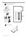
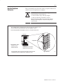
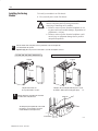
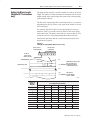
( P2–4
Using This Manual
Table of Contents
)"15&3 #+&$5*7&4 0%6-& &4$3*15*0/ &"563&4 30(3". &-&$5"#-& /165 "/(&4 08 /"-0( 0%6-&4 0..6/*$"5& 8*5) 30(3".."#-& 0/530--&34
0..6/*$"5*0/ &58&&/ 30$&4403 "/% 0%6-& $$63"$9 )"15&3 6.."39 )"15&3 #+&$5*7&4 0.1-*"/$& 50
6301&"/ /*0/ *3&$5*7&4 *3&$5*7& 08 0-5"(& *3&$5*7& &'03& !06 /45"-- !063 /165 0%6-& -&$53045"5*$ "."(& 08&3 &26*3&.&/54 0$"5*/( 5)& 0%6-& */ 5)& )"44*4 &55*/( 5)& 0/'*(63"5*0/ -6(4 0/ 5)& 0%6-& &9 5)& "$,1-"/& 0//&$503 /45"--*/( 5)& /"-0( 0%6-& *3*/( !063 /"-0( /1650%6-& */*.*:*/( 306/% 0014 "#-& &/(5)4 306/%*/( /%*$"503 *()54 )"15&3 6.."39 )"15&3 #+&$5*7&4 -0$, 3"/4'&3 30(3"..*/( ; 30(3"..*/( ; 30(3"..*/( 0%6-& $"/ *.& )"15&3 6.."39 6#-*$"5*0/ ; 6-9 Table of Contents
*#26'4 $,'%6+8'5 10(+)74+0) "174 0276 1&7.' 0276 #0)' '.'%6+10 0276 #0)' '.'%6+10 +65 0276 1.6#)' #0& 744'06 #0)'5 (14 6*' #56 0#.1)
0276 1&7.' 0276 :2' '.'%6+0) +0).';'0&'& 14 +(('4'06+#. 02765 #6# 14/#6 '.'%6+0) 6*' #6# 14/#6 915 %1/2.'/'06 $+0#4: &#6# (+456 +)+6#. +.6'4+0) '#. +/' #/2.+0) +6 '66+0)5 (14 6*' '#. +/' #/2.' 1&' %#.+0) /2.'/'06+0) 6*' %#.+0) '#674' %#.+0) #0)'5 .1%- 4#05('4 '#& #0& !4+6' +.' '0)6*5 8'45#/2.+0) *#00'. +5#$.' '(#7.6 10(+)74#6+10 *#26'4 7//#4: *#26'4 $,'%6+8'5 '#&+0) #6# 41/ "174 1&7.' .1%- 4#05('4 '#& 14/#6 #6# +456 10(+)74#6+10 *#26'4 7//#4: *#26'4 $,'%6+8' !*'0 #0& 19 61 #.+$4#6' "174 0#.1) 0276 1&7.' 11.5 #0& 37+2/'06 *'%-+0) 1&7.' #.+$4#6+10 #.+$4#6+0) :174 0276 1&7.' ((5'6 #.+$4#6+10 !4+6' .1%- 4#05('4 !14& (14 ((5'6 #.+$4#6+10 '#& .1%- 4#05('4 !14& !4+6' .1%- 4#05('4 !14& (14 #+0 #.+$4#6+10 '#& .1%- 4#05('4 !14& *#26'4 7//#4: 7$.+%#6+10 ;
7.: iii
Table of Contents
Troubleshooting Your Input
Module
Specifications
Chapter 7
Chapter Objective . . . . . . . . . . . . . . . . . . . . . . . . . . . . . . . . . . . .
Diagnostics Reported by the Module . . . . . . . . . . . . . . . . . . . . . . .
Diagnostic Bits Reported By the Analog Input Module . . . . . . . . .
Troubleshooting Chart for the Fast Analog
Input Module (1771ĆIFF/A) . . . . . . . . . . . . . . . . . . . . . . . .
CheckingModule Operation . . . . . . . . . . . . . . . . . . . . . . . . . . . . .
Connect the Module in a Simple Test System . . . . . . . . . . . . . . .
Troubleshooting a Bad Input . . . . . . . . . . . . . . . . . . . . . . . . . . . . .
Measuring Each Input with Respect to Module Common . . . . . . .
Disconnecting Inputs from the Field Wiring Arm One at a Time While
Observing Module Action . . . . . . . . . . . . . . . . . . . . . . . . . .
Testing for Input Channel Functionality . . . . . . . . . . . . . . . . . . .
Chapter Summary . . . . . . . . . . . . . . . . . . . . . . . . . . . . . . . . . . . .
7-8
7-9
7-9
A-1
A-2
A-4
Appendix B
Sample Programs for the Analog Input Module . . . . . . . . . . . . . . . .
PLCĆ2 Family Processors . . . . . . . . . . . . . . . . . . . . . . . . . . . . . . .
PLCĆ3 Family Processor . . . . . . . . . . . . . . . . . . . . . . . . . . . . . . .
PLCĆ5 Family Processors . . . . . . . . . . . . . . . . . . . . . . . . . . . . . . .
Data Table Formats
7-3
7-4
7-4
7-7
7-7
Appendix A
Specifications . . . . . . . . . . . . . . . . . . . . . . . . . . . . . . . . . . . . . . .
Module Scan Time . . . . . . . . . . . . . . . . . . . . . . . . . . . . . . . . . . . .
Resolution . . . . . . . . . . . . . . . . . . . . . . . . . . . . . . . . . . . . . . . . . .
Programming Examples
7-1
7-1
7-1
B-1
B-1
B-2
B-4
Appendix C
4ĆDigit Binary Coded Decimal (BCD) . . . . . . . . . . . . . . . . . . . . . . .
..................................................
..................................................
Block Transfer (MiniĆPLCĆ2
and PLCĆ2/20 Processors)
Appendix D
Forms
Appendix E
Multiple GET Instructions Ć MiniĆPLCĆ2 and PLCĆ2/20 Processors . .
Setting the Block Length (Multiple GET Instructions only) . . . . . . . .
Forms . . . . . . . . . . . . . . . . . . . . . . . . . . . . . . . . . . . . . . . . . . . . .
C-1
C-2
C-3
D-1
D-3
E-1
Publication 1771Ć6.5.116 - July 1996
Table of Contents
! !#
In this chapter, we describe:
• checking your calibration
• calibrating your module.
$ !
! " "! "
Your module is shipped to you already calibrated. If you are
checking calibration, or if it becomes necessary to recalibrate the
module, you must do so with the module in an I/O chassis. The
module must communicate with the processor and industrial
terminal.
Before calibrating the module, you must enter ladder logic into the
processor memory, so that you can initiate BTWs to the module, and
the processor can read inputs from the module.
Periodically (frequency based on your application), check your
module calibration. Calibration may be required to remove module
error due to aging of components in your system.
Calibration can be accomplished using either of two methods:
• manual calibration, as described below.
• 6200 I/O CONFIGURATION software – refer to your 6200
software publications for procedures for calibrating.
When calibrating your module, you must perform:
• offset calibration first
• gain calibration second
"!
"!
In order to calibrate your input module you will need the following
tools and equipment:
!
%
# ,!%-%)( )&.#! )/,!
' µ ,!-)&/.%)(
(&)#% . ,!%-%)( ), !+/%0&!(.
( /-.,%& !,'%(& (
(.!,)((!. &!
,)#,''%(# .!,'%(& "), "'%&1 *,)!--),-
. ) ), . )
!.
&&!(, &!1 )'*(1
1"%!& !%#$.- /&%.%)( 2
/&1 1–2
Calibrating Your Module
If a calibration check of your module becomes necessary:
1. Verify that the module is in voltage mode. In single-ended mode,
apply voltages to channels 1 through 16.
2. Send a configuration block transfer write to the module that
replicates the specific application. (This forces the module to do
an internal calibration.)
3. Apply –10V, –5V, –2.5V 0V, 1V, 2.5V, 5V, and 10V to the
module. In differential, apply voltages to channels 1 through 8
Verify that the values returned are within 0.1% of bipolar full
scale.
4. If values are within tolerance, no calibration is necessary. If not,
perform calibration below.
Calibrating Your Module
Calibrating your Input
Module
1–3
The fast analog input module is shipped already calibrated.
Calibration of the module consists of applying a voltage or current
across each input channel for offset and gain calibration. Offset and
gain values are shown in the following table.
Table 1.A
Offset and Gain Values for Calibrating the 1771ĆIFF/A Fast
Analog Input Module
SingleĆended
Range
Differential
Offset Value
Gain Value
Offset Value
Gain Value
" " " " " " " " Offset Calibration
Normally all inputs are calibrated together. To calibrate the offset of
an input, proceed as follows:
1. Apply power to the module.
2. Apply the offset voltage of 0V or current of 0.000mA (Table 1.A)
as required to all 16 channels (8 in differential mode).
3. After the connections stabilize, set all bits in write word 38 to 1
and all bits in word 39 to 0. Send a 39 word block transfer write
(BTW) to the module to calibrate the offset. Refer to chapter 4.(In
Differential mode, the upper byte of word 38 is not set (bits 8–15
decimal or 10–17 octal are 0).)
"! When the BTW is sent, all channels are calibrated to 0.000V.
Write Block Transfer Word 38 for Offset Calibration
Decimal Bits
15
14
13
12
11
10
09
08
07
06
05
04
03
02
01
00
Octal Bits
17
16
15
14
13
12
11
10
07
06
05
04
03
02
01
00
! #" %
#$ 1–4
Calibrating Your Module
The BTR echoes back the status of each of the channels to verify
calibration. If selected channels were calibrated satisfactorily, the
BTR will reflect this by having their bits set to 1. (In Differential
mode, the upper byte of word 21 in the BTR is not set (bits 8–15
decimal or 10–17 octal are 0).)
! "!
" "!
4. Proceed to Gain Calibration below.
"
Calibrating gain requires that you apply 5.000V, 10.000V or 20mA
(as determined by your range and mode) (Table 1.A) across each
input channel.
1. Apply power to the module.
2. Apply the gain voltage as shown in Table 1.A to all 16 channels
(single-ended) or 8 channels (differential).
3. After the connections stabilize, request the gain calibration by
sending a 39 word block transfer write (BTW) to the module.
Refer to chapter 4.
When the BTW is sent, all selected channels are calibrated (set to
1) shown in Table 1.A. If a channel is not selected for
calibration, its bit is 0. (In Differential mode, the upper byte of
word 39 is not set (bits 8–15 decimal or 10–17 octal are 0).) All
bits in word 38 will be set to 0.
" ! "
"!
" "!
!
Calibrating Your Module
1–5
The BTR echoes back the status of each of the channels to verify the
calibration. If all channels were calibrated satisfactorily, the BTW
will reflect this by having all bits set to 1.
Read Block Transfer Word 22
Decimal Bits
15
14
13
12
11
10
09
08
07
06
05
04
03
02
01
00
Octal Bits
17
16
15
14
13
12
11
10
07
06
05
04
03
02
01
00
Chapter Summary
In this chapter, you learned how to calibrate your input module.
1–6
Calibrating Your Module
In this chapter, we describe how to troubleshoot your fast analog
module by:
•
•
•
•
•
observing the indicators
monitoring status bits reported to the processor.
checking module operation
checking for common mode voltages
isolating a bad input
At power-up, the module momentarily turns on the red indicator as a
lamp test, then checks for:
• correct RAM operation
• firmware errors
Thereafter, the module lights the green RUN indicator when
operating without fault, or lights the red FAULT indicator when it
detects fault conditions. The module also reports status and specific
faults (if they occur) in every transfer of data (BTR) to the PC
processor. Monitor the green and red indicators and status bits in
word 1 of the BTR file when troubleshooting your module.
&
Diagnostic bits in the read block transfer status words provide
diagnostic capabilities.
Word 1 provides power-up and valid data status. Words 2, 3 and 4
provide channel data status.
If a module on-board self test fault occurs, block transfers will be
inhibited, the red fault (FLT) will light, and the green run (RUN)
light will go out.
Word 1
Diagnostics word 1 is the first data word in the read block transfer
file for transfer to the central processor. It contains a power-up bit
(bit 00) that is set (1) when the module is first powered up. It is reset
(0) after a write block transfer. It also contains an under-range or
over-range bit (bit 01) that is set when any input is under or
over-range.
$ #"! &
$ % 2–2
Troubleshooting Your Input Module
An invalid scaling data bit (bit 02) is set if invalid scaling data is
entered into any of the minimum/maximum scaling value words.
Note that minimum equal to maximum is an invalid value. If
invalid values are entered into the minimum or maximum scaling
words the corresponding read block transfer input channel word will
be set to 0000.
Bit 02 is set if an invalid digital filter value is entered (e.g., 1F). If an
invalid digital filter value is entered, the module will not perform
digital filtering.
The real time sample (RTS) fault bit (bit 03) is set if the module is
configured for RTS and a block transfer read has not occurred within
the user-programmed period.
Bit 04 is the calibration status bit. This bit is reset (0) when a
successful calibration is completed. If the bit is set (1), an incorrect
voltage/current was applied, or offset and gain calibrations were
attempted together.
The EEPROM status bit (05) is set when an error occurs when
saving calibration data to nonvolatile memory. If this bit is set at
powerup, the EEPROM data did not pass checksum and calibration
values are being used.
The hardware failure bit (06) is set when a blown fuse is detected,
or when the EEPROM can’t recover from a fault.
Word 2
Word 2 provides for under-range conditions. When a particular
channel input is under-range, the associated bit will be set. As long
as inputs are under range the associated bit remains set. Bit 00
corresponds to channel 1, bit 01 to channel 2, etc.
Word 3
Word 3 provides for over-range conditions. When a particular
channel input is over-range, the associated bit will be set. As long as
inputs are in range the associated bit remains reset. Bit 00
corresponds to channel 1, bit 01 to channel 2, etc.
Word 4
Word 4 provides an indication of a particular channel’s input polarity
(set, or 1 = negative; reset, or 0 = positive). Bit 00 corresponds to
channel 1, bit 01 to channel 2, etc.
Troubleshooting Your Input Module
2–3
The following table lists the probable cause and recommended
actions for some common trouble indications.
! ! ! "
""
)
'%)&%)#
!
#,!!)
,! *,(' *+!,.%*)
*)!
'%)&%)#
*""
1%.%)# *)"%#/,.%*) '*& ,)-"!,
,%.!
!) *)"%#/,.%*) #,!!)
,! , 1,! "%'/,! %) (* /'!
!./,) (* /'! "*, ,!+%,
* +*1!,
/,) *"" +*1!, !(*0! ) ,!%)-!,.
(* /'! %).* $--%- !./,) +*1!,
" +,*'!( -.%'' !2%-.- ) $--%- +*1!,
-/++'3 %- "/).%*)%)# +,*+!,'3 ,!./,) .$!
(* /'! "*, ,!+%,
!%.$!, *(!- *)
/'%.%*) 4 /'3 2–4
Troubleshooting Your Input Module
The following allows you to run a check on module operation, and
isolate a fault either to the module or external to the module.
Set up a 1771 I/O chassis with a PLC-5 processor in the leftmost
slot.
Set the chassis backplane switch 5 to ON. All other backplane switches to Off.
This sets the chassis to 1Ćslot addressing.
Note: Check the processor screen to verify that the processor is set for 1Ćslot addressing.
Off
Off
Always Off
Always Off
5
6
OFF
OFF
2Ćslot
ON
OFF
1Ćslot 1
OFF
ON
1/2 slot 1,2
ON
ON
Not allowed
Pressed in
at top ON (closed)
Pressed in
at top OFF (open)
Place the module in the card guides on the top and bottom of the first slot next to the
processor. These slots guide the 1771ĆIFF/A module into position.
Apply firm even pressure on the module to seat it into its backplane connector.
1771ĆA1B, ĆA2B, ĆA3B, ĆA3B1, ĆA4B I/O chassis
1771ĆA1B, ĆA2B, ĆA3B1, ĆA4B Series B I/O chassis
locking bar pin
locking tab
locking bar
card guides
card guides
PLCĆ5 Processor
IFF module
Snap the chassis latch over
the top of the module to secure it.
PLCĆ5 Processor
After inserting the module into the slot, apply power to the chassis.
Publication 1771Ć6.5.116 - July 1996
IFF module
Swing the chassis locking bar down into place to secure
the modules. Make sure the locking pins engage. 19809
Troubleshooting Your Input Module
2–5
Enter the following ladder logic into the processor.
BT9:0
BT9:1
EN
EN
1
Note: This programming is only to test
the block transfer write and read functions.
It is not intended for regular use.
BT9:1
BT9:0
EN
EN
BTW
BLOCK TRANSFER WRITE
RACK:
00
0
GROUP:
0
MODULE:
BT9:0
CONTROL BLOCK:
N7:0
DATA FILE:
LENGTH:
0
CONTINUOUS:
N
DN
ER
BTR
BLOCK TRANSFER READ
RACK:
00
0
GROUP:
0
MODULE:
BT9:1
CONTROL BLOCK:
N7:40
DATA FILE:
LENGTH:
0
CONTINUOUS:
N
EN
DN
ER
The module lights the green RUN indicator when operating
without fault, or lights the red FAULT indicator when it detects
fault conditions.
FAST
ANALOG
(12 BIT)
If the module is operating correctly, the module will
be receiving BTRs and sending BTWs. The indiĆ
cator light will indicate grenn/flashing green.
RUN
If the indicator is blinking green, the module
has not received a configuration block transfer
write.
EN
FLT
This configuration sets the 1771ĆIFF module for:
1Ć5V range
SingleĆended inputs
BCD data format
No digital filter
No real time sampling
0-4095 scaling
8 X oversample
No disabled channels
Block Transfer Write
Data Table Report
Monitor the status bits in word 1 of the
BTR file when troubleshooting your
module.
Write block transfer
configuration data
Read block
transfer data
Note: 1653310 = 409516 (BCD)
ADDRESS
0
N7:0
0
N7:10 16533
N7:20 16533
N7:30 16533
2
N7:40
0
N7:50
0
N7:60
0
N7:70
0
N7:80
0
N7:90
0
N7:100
PLCĆ5/11
1
2
0
0
0 16533
0 16533
0 16533
-1
0
0
0
0
0
0
0
0
0
0
0
0
0
Addr 4 IFF
3
Data Table File N7:0
4
5
6
0
0
0 16533
0 16533
0 16533
0
0
0
0
0
0
0
0
0
0
0
0
0
0
0
0
0
0
0
0
0
0
0
0
0
16533
16533
16533
16533
0
0
0
0
0
0
0
7
8
9
0 16533
0 16533
0 16533
0
0
0
0
0
0
0
0
0
0
0
0
0
0
0
0
0
0
0
0
0
0
0
0
0
0
0
Note: If all input terminals are shorted together and tied to module common, the input data for all channels will read zero.
Publication 1771Ć6.5.116 - July 1996
2–6
Troubleshooting Your Input Module
The module also reports status and specific faults (if they occur) in every transfer of data (BTR) to
the PC processor. Monitor the green and red indicators and the status bits in word 1 of the BTR file
when troubleshooting your module.
Data Table Report PLCĆ5/11
Addr 4 IFF
Data Table File N7:0
ADDRESS EN ST DN ERCO EW NR TO RWRLEN DLEN FILE ELEM R G M
Block transfer control files
BT9:0
BT9:1
BT9:2
0 1 1
1 1 0
0 0 0
0 0
0 0
0 0
1 1
1 1
0 0
Memory Map Report PLCĆ5/11
FILE
0
1
2
3
4
5
6
7
8
9
TYPE
0
0
0
0
1
0
0
0
0
Addr 4 IFF
LAST ADDRESS
37
20
0
7
7
0
0 0 0 0
40 0 0 0
0 0 0 0
Data Table File N7:0
SIZE (elements) SIZE (words)
O
I
S
B
T
C
R
N
F
output
input
status
binary or bit
timer
counter
control
integer
floating point
O:037
I:037
S:127
B3/15
T4:0
C5:0
R6:0
N7:103
F8:0
32
32
128
1
1
1
1
104
1
38
38
134
7
9
9
9
110
8
BT
block transfer
BT9:2
3
24
Attach the wiring arm (1771ĆWG) to the horizontal
bar at the bottom of the I/O chassis.
wiring arm
The wiring arm pivots upward and connects with
the module so you can install or remove the
module without disconnecting the wires.
1771ĆWG
remove
horizontal bar
After connecting the field wiring arm to the module,
proceed to check the module operation when receivĆ
ing inputs.
Publication 1771Ć6.5.116 - July 1996
Troubleshooting Your Input Module
2–7
After determining that the module is operating correctly,
troubleshoot any faulty inputs by:
• measuring each input with respect to module common
• disconnecting inputs from the field wiring arm one at a time
while observing module action
• testing for input channel functionality
During this procedure, monitor the input data table of the
programmable controller and observe any changes which occur.
1. Make sure the field wiring arm is in position on the module.
2. Apply power to the 1771 I/O chassis.
3. Check each input (either single-ended or differential) for common
mode voltages exceeding +35V with respect to module common.
A. Hold the positive probe of the voltmeter on the first input
terminal.
B. Hold the negative probe of the voltmeter on a module
common terminal (terminals 20 or 21).
4. If any voltage is seen that exceeds +35V, remove that channel’s
input wiring and observe the affect on the input data table of the
programmable controller.
!
ATTENTION: Remove power from the 1771 I/O
chassis backplane and field wiring arm before
removing or installing input wiring.
• Failure to remove power from the backplane or
wiring arm could cause module damage, degradation
of performance, or injury.
• Failure to remove power from the backplane could
cause injury or equipment damage due to possible
unexpected operation.
If no other common mode voltages are present, the input data for
all other channels should stabilize to some predictable value.
2–8
Troubleshooting Your Input Module
5. Attempt to equalize all grounds at the offending channel before
reconnecting the input wiring.
!
ATTENTION: Remove power from the 1771 I/O
chassis backplane and field wiring arm before
removing or installing input wiring.
• Failure to remove power from the backplane or
wiring arm could cause module damage, degradation
of performance, or injury.
• Failure to remove power from the backplane could
cause injury or equipment damage due to possible
unexpected operation.
6. If the common mode voltage cannot be removed on the input, an
isolation device may be required on that channel.
During this procedure, monitor the input data table of the
programmable controller and observe any changes which occur.
1. Make sure the field wiring arm is in position on the module.
2. Apply power to the 1771 I/O chassis.
3. While observing the input data table, remove one input at a time.
!
ATTENTION: Remove power from the 1771 I/O
chassis backplane and field wiring arm before
removing or installing input wiring.
• Failure to remove power from the backplane or
wiring arm could cause module damage, degradation
of performance, or injury.
• Failure to remove power from the backplane could
cause injury or equipment damage due to possible
unexpected operation.
4. When the offending input channel is disconnected, the input data
table will stabilize to some predictable values.
Troubleshooting Your Input Module
2–9
To test the functionality of an input channel:
1. Remove the input wiring from the field wiring arm.
!
ATTENTION: Remove power from the 1771 I/O
chassis backplane and field wiring arm before
removing or installing input wiring.
• Failure to remove power from the backplane or
wiring arm could cause module damage, degradation
of performance, or injury.
• Failure to remove power from the backplane could
cause injury or equipment damage due to possible
unexpected operation.
2. Connect a battery (or other voltage source) across the input
terminals. When the 4-20mA range is selected, the voltage source
must not exceed 1-5V.
!
ATTENTION: The voltage source must be within the
selected voltage range. If the source voltage is greater
than the selected voltage range of the input, module
damage will result.
3. Monitor the input data table for predictable values.(values relative
to the input source voltage).
In this chapter you learned how to interpret the indicator lights, and
troubleshoot your input module.
2–10
Troubleshooting Your Input Module
Overview of the Fast Analog
Input Module
This chapter, we describe:
• features of the module
• how the module communicates with programmable controllers
The fast analog input module is an intelligent block transfer module
that interfaces analog input signals with any Allen-Bradley
programmable controllers that have block transfer capability. Block
transfer programming moves input data words from the module’s
memory to a designated area in the processor data table in a single
scan. It also moves configuration words from the processor data
table to module memory.
The fast analog input module is a single-slot module and requires no
external power supply. (If using passive transducers for input, the
user must supply loop power.) After scanning the analog inputs, the
input data is converted to a specified data type in a digital format to
be transferred to the processor’s data table on request. The block
transfer mode is disabled until this input scan is complete.
Consequently, the minimum interval between block transfer reads is
the same as the total input update time for each analog input module.
The fast analog input module senses up to 16 single-ended or 8
differential analog inputs and converts them to a proportional
four-digit BCD or twelve-bit binary value. You can select from five
voltage or three current input ranges. Each input can be configured
as a current or voltage input with internal jumpers.
This module’s program selectable features include:
• 16 single-ended or 8 differential inputs
• User program selectable input ranges on a per channel basis (see
•
•
•
•
•
•
table)
Selectable real-time sampling
Selectable scaling to engineering units
Selectable digital filtering
Selectable data format
Selectable oversampling
Selectable channel disable
3–2
Overview of the Fast Analog Input Module
&" &" &" &" ) &" ) &" ) &" &" The processor transfers data to the module (block transfer write) and
from the module (block transfer read) using BTW and BTR
instructions in your ladder diagram program. These instructions let
the processor obtain input values and status from the module, and let
you establish the module’s mode of operation.
1. The processor transfers your configuration data to the module via
a block transfer write instruction.
2. External devices generate analog signals that are transmitted to
the module.
%%%
#!
)
Fast Analog Input
Module
Cat. No. 1771-IFF
'&"! ) ( $"%%"$
)
Overview of the Fast Analog Input Module
3–3
3. The module converts analog signals into binary or BCD format,
and stores theses values until the processor requests their transfer.
4. When instructed by your ladder program, the processor performs
a read block transfer of the values and stores them in a data table.
5. The processor and module determine that the transfer was made
without error, and that input values are within specified range.
6. Your ladder program can use and/or move the data (if valid)
before it is written over by the transfer of new data in a
subsequent transfer.
7. Your ladder program should allow write block transfers to the
module only when enabled by operator intervention or at
power-up.
The accuracy of your input module is described in Appendix A.
In this chapter you read about the functional aspects of the input
module and how the module communicates with the programmable
controller.
3–4
Overview of the Fast Analog Input Module
Installing the Input Module
In this chapter, we tell you about:
•
•
•
•
•
•
calculating the chassis power requirement
choosing the module’s location in the I/O chassis
configuring your module configuration plugs
keying a chassis slot for your module
installing the input module
wiring the input module’s field wiring arm
If this product has the CE mark it is approved for installation within
the European Union and EEA regions. It has been designed and
tested to meet the following directives.
This product is tested to meet Council Directive 89/336/EEC
Electromagnetic Compatibility (EMC) and the following standards,
in whole or in part, documented in a technical construction file:
• EN 50081-2EMC – Generic Emission Standard, Part 2 –
Industrial Environment
• EN 50082-2EMC – Generic Immunity Standard, Part 2 –
Industrial Environment
This product is intended for use in an industrial environment.
This product is tested to meet Council Directive 73/23/EEC
Low Voltage, by applying the safety requirements of EN 61131–2
Programmable Controllers, Part 2 – Equipment Requirements and
Tests.
For specific information required by EN 61131-2, see the appropriate
sections in this publication, as well as the following Allen-Bradley
publications:
• Industrial Automation Wiring and Grounding Guidelines For
Noise Immunity, publication 1770-4.1
• Guidelines for Handling Lithium Batteries, publication AG-5.4
• Automation Systems Catalog, publication B111
Before installing your input module in the I/O chassis:
%.%- -" )(/+ +*.#+&'-, ( %%
&(.%, #' " ",,#,
(/+ *.#+&'-, )! -+&#' /"+ -( )% -" &(.% #' -" ",,#,
(.% (-#(' #' -" ",,#,
)! 0 -" $)%' (''-(+ #' -" ",,#,
(.% 0#'! )! $ (''-#(', -( -" /#+#'! +&
#+#'! (.+ ').- (.% )! ' +(.'#'! )! The 1771-IFF/A module is shipped from the factory
set for voltage mode. Refer to “Setting the
Configuration Plugs on the Module”on page 4–3 for
other combinations of current and voltage inputs.
Electrostatic discharge can damage semiconductor devices inside this
module if you touch backplane connector pins. Guard against
electrostatic damage by observing the following precautions:
!
ATTENTION: Electrostatic discharge can degrade
performance or cause permanent damage. Handle the
module as stated below.
• Wear an approved wrist strap grounding device, or touch a
grounded object to rid yourself of electrostatic charge before
handling the module.
• Handle the module from the front, away from the backplane
connector. Do not touch backplane connector pins.
• Keep the module in its static-shield bag when not in use.
! Your module receives its power through the 1771 I/O power supply.
The module requires 500mA from the backplane.
Add this current to the requirements of all other modules in the I/O
chassis to prevent overloading the chassis backplane and/or
backplane power supply.
.%#-#(' 1
.' Place your module in any I/O module slot of the I/O chassis except
for the extreme left slot. This slot is reserved for PC processors or
adapter modules.
Group your modules to minimize adverse affects from radiated
electrical noise and heat. We recommend the following.
• Group analog input and low voltage dc modules away from ac
modules or high voltage dc modules to minimize electrical noise
interference.
• Do not place this module in the same I/O group with a discrete
high-density I/O module when using 2-slot addressing. This
module uses a byte in both the input and output image tables for
block transfer.
The fast analog input module (1771-IFF/A) has configuration plugs
for determining the input type (voltage or current) desired for each
input. The module comes from the factory with the configuration
plugs positioned for voltage mode.
Note that you can select either voltage or current for each input, but
they must all be either single-ended or all differential.
Do not mix single-ended and differential inputs on
the module.
To set the configuration plugs for your desired inputs:
! &%) * %$ * %$ +(* %$ &"+) ))% * - * $&+* $$" %( $ *% /%+( ('+ (#$*)
%+ $ # . ,%"* #% $ +(($* #%
)** $) %$ * #%+" ! )+( ** *
$* ( #%+" ) )* %( *( ) $"0$ %(
($* " % $%* # . *#
$$" +(($*
,$ $$" ,%"*
$$"
$ $$"
$ $$"
$ $$"
$ $$"
$ $$"
$ $$"
$ $$"
$ $$" $$" $$" $$" $$" Selection
Plugs
$$" $$" $$" ,$ $$" +(($*
0
$$" ,%"*
&%) * %$ * %,( $ )+( - *
* %+() )(-) (#%, $ )*& +" * %$ 0
+$ Place your module in any slot in the chassis except the leftmost slot
which is reserved for processors or adapters.
!
ATTENTION: Observe the following precautions
when inserting or removing keys:
• insert or remove keys with your fingers
• make sure that key placement is correct
Incorrect keying or the use of a tool can result in
damage to the backplane connector and possible
system faults.
/ #%+" ) )"%** * *-% &") %$ * (( % * (+ * %( )
)"%*) #* - * &")* !. $ $) - #%+$* %$ * !&"$ %$$*%(
%) * %$ * !. $ $) $ * !&"$ %$$*%( *% %(()&%$ *% * !. )"%*)
)) )
. $ $)
*-$ $ *-$ $ $)(* %( (#%,
!. $ $) - * .%+( $()
!. $ $) $ (&%) * %$ )+)'+$* ).)*# ) $ $
(- ( $ #! $)(* %$ % ($* *.& % #%+" $))(.
&&( %$$*%(
/
+" * %$ /
+$ To install your module in an I/O chassis:
1. First, turn off power to the I/O chassis:
ATTENTION: Remove power from the 1771 I/O
chassis backplane and field wiring arm before
removing or installing an I/O module.
!
• Failure to remove power from the backplane or wiring arm could cause module damage, degradation of
performance, or injury.
• Failure to remove power from the backplane could
cause injury or equipment damage due to possible
unexpected operation.
Place the module in the card guides on the top and bottom of the slot that guide the
1771ĆIFF/A module into position.
Apply firm even pressure on the module to seat it into its backplane connector.
1771ĆA1B, ĆA2B, ĆA3B, ĆA3B1, ĆA4B I/O chassis
1771ĆA1B, ĆA2B, ĆA3B1, ĆA4B Series B I/O chassis
locking bar pin
locking tab
locking bar
card guides
card guides
IFF module
IFF module
Snap the chassis latch over
the top of the module to secure it.
Swing the chassis locking bar down into place to secure
the modules. Make sure the locking pins engage. 19809
Attach the wiring arm (1771ĆWG) to the horizontal
bar at the bottom of the I/O chassis.
wiring arm
The wiring arm pivots upward and connects with
the module so you can install or remove the
module without disconnecting the wires.
remove
horizontal bar
Publication 1771Ć6.5.116 - June 1996
1771ĆWG
17643
Connect your I/O devices to the cat. no. 1771-WG wiring arm
shipped with the module. The wiring arm is attached to the pivot bar
at the bottom of the I/O chassis. It pivots upward and connects with
the module so you can install or remove the module without
disconnecting the wires.
!
ATTENTION: Remove power from the 1771 I/O
chassis backplane and field wiring arm before
removing or installing an I/O module.
• Failure to remove power from the backplane or wiring arm could cause module damage, degradation of
performance, or injury.
• Failure to remove power from the backplane could
cause injury or equipment damage due to possible
unexpected operation.
Input connections for the 1771-IFF/A module with single-ended
inputs are shown in Figure 4.1 and Figure 4.2. Input connections for
the 1771-IFF/A with differential inputs are shown in Figure 4.3 and
Figure 4.4.
To minimize ground-loop currents on input circuits:
• use single-ended mode whenever possible
• use 2-wire transmitters with a common power supply
• separate 2-wire and 4-wire transmitters between different
modules
• tie 4-wire transmitter and/or separate power supply grounds
together
We do not recommend mixing 2-wire and 4-wire
transmitter inputs on the same module. Power supply
placement can make it impossible to eliminate ground
loops.
Recommended maximum cable length for voltage-mode input
devices is 50 feet. This recommendation is based on considerations
of signal degradation and electrical noise immunity in typical
industrial environments. Cable length for current-mode input
devices need not be as restrictive because analog signals from these
devices are less sensitive to electrical noise interference.
" !" Channel 1
Refer to transmitter manufacturers
specifications for power supply connections.
2Channel
Power
Supply
2ĆWire
Transmitter
Power
Supply
2
3
3
Channel 4
+
2ĆWire
Transmitter
1
Channel 2
1Module
-
Common
Channel 5
7
Channel 7
8
Channel 8
1Module
Common
Channel 9
together inside the module.
Source Ground
2 Jumper all unused channels to
module common to reduce noise.
power supply grounds together to
minimize ground loops.
3 Tie
13
Channel 12
Common
Channel 13
The shield should extend to the termination point,
exposing just enough cable to adequately terminate the
inner conductors. Use heat shrink or another suitable
insulation where the wire exits the cable jacket.
Publication 1771Ć6.5.116 - June 1996
15
17
18
Channel 16
The sensor cable must be shielded. The shield must:
• extend the length of the cable, but be connected only at the 1771
I/O chassis
• extend up to the point of termination
14
16
Channel 14
Channel 15
The 1771ĆIFF module does not supply loop power for the input device. The user
must supply loop power for loopĆpowered input devices.
10
12
Channel 11
1Module
9
11
Channel 10
1 All commons are electrically tied
5
6
Channel 6
+
_
4
1Module
Common
1Module
Common
19
20
21
1771ĆWG
Field Wiring Arm
10948ĆI
! " ! !" Channel 1
Refer to transmitter manufacturers
specifications for power supply connections.
Power
Supply
Power
Supply
4ĆWire
Transmitter
4ĆWire
Transmitter
Channel 2
2Channel
3
Channel 4
+
1Module
-
Common
Channel 5
Channel 6
+
Channel 7
-
Channel 8
1Module
Common
Channel 9
Channel 10
1 All commons are electrically tied
Source Ground
together inside the module.
2 Jumper all unused channels to
module common to reduce noise.
3 Tie
power supply grounds together to
minimize ground loops.
Channel 11
Channel 12
1Module
Common
Channel 13
Channel 14
Channel 15
Channel 16
The 1771ĆIFF module does not supply loop power for the input device. The user must supply
loop power for loopĆpowered input devices.
The sensor cable must be shielded. The shield must:
• extend the length of the cable, but be connected only at the 1771
I/O chassis
• extend up to the point of termination
1Module
Common
1Module
Common
1
2
3
4
5
6
7
8
9
10
11
12
13
14
15
16
17
18
19
20
21
1771ĆWG
Field Wiring Arm
10948ĆI
The shield should extend to the termination point,
exposing just enough cable to adequately terminate the
inner conductors. Use heat shrink or another suitable
insulation where the wire exits the cable jacket.
Publication 1771Ć6.5.116 - June 1996
" ! ! "! #$
!!
Channel 1+
! Refer to transmitter manufacturers
specifications for power supply connections.
2ĆWire
Transmitter
Power
Supply
2ĆWire
Transmitter
2
Channel 2+
+
Channel 2Ć
-
Not used
3
4
5
Channel 3+
6
Channel 3Ć
+
Power
Supply
1
Channel 1Ć
7
Channel 4+
-
8
Channel 4Ć
9
Not used
10
Channel 5+
11
Channel 5Ć
1. Unused channels must have their + and Ć inputs jumpered
together and tied to module common to reduce noise.
2 Tie power supply grounds together to
minimize ground loops.
Source Ground
The 1771ĆIFF module does not supply loop power for the input device. The user must supply
loop power for loopĆpowered input devices.
12
Channel 6+
13
Channel 6Ć
14
Not used
15
Channel 7+
16
Channel 7Ć
17
Channel 8+
18
Channel 8Ć
Configuring the module for differential inputs does not provide isolation.
Module Common
Module Common
The sensor cable must be shielded. The shield must:
• extend the length of the cable, but be connected only at the 1771
I/O chassis
• extend up to the point of termination
!! The shield should extend to the termination point,
exposing just enough cable to adequately terminate the
inner conductors. Use heat shrink or another suitable
insulation where the wire exits the cable jacket.
Publication 1771Ć6.5.116 - June 1996
10949ĆI
19
20
21
1771ĆWG
Field Wiring Arm
! Channel 1+
Power
Supply
4ĆWire
Transmitter
1
Channel 1Ć
Refer to transmitter manufacturers
specifications for power supply connections.
2
Channel 2+
+
Channel 2Ć
-
Not used
3
4
5
Channel 3+
Power
Supply
4ĆWire
Transmitter
6
Channel 3Ć
+
7
Channel 4+
-
8
Channel 4Ć
9
Not used
10
Channel 5+
11
Channel 5Ć
1. Unused channels must have their + and Ć inputs jumpered
together and tied to module common to reduce noise.
Source Ground
2 Tie
power supply grounds together to
minimize ground loops.
The 1771ĆIFF module does not supply loop power for the input device. The user must supply
loop power for loopĆpowered input devices.
12
Channel 6+
13
Channel 6Ć
14
Not used
15
Channel 7+
16
Channel 7Ć
17
Channel 8+
18
Channel 8Ć
Module Common
Configuring the module for differential inputs does not provide isolation.
Module Common
The sensor cable must be shielded. The shield must:
• extend the length of the cable, but be connected only at the 1771
I/O chassis
• extend up to the point of termination
The shield should extend to the termination point,
exposing just enough cable to adequately terminate the
inner conductors. Use heat shrink or another suitable
insulation where the wire exits the cable jacket.
19
20
21
1771ĆWG
Field Wiring Arm
10949-I
Publication 1771Ć6.5.116 - June 1996
When using shielded cable wire, ground the foil shield and drain
wire only at one end of the cable. We recommend that you wrap the
foil shield and drain wire together, and connect them to a chassis
mounting bolt, grounding stud or chassis single-point grounding
point (Figure 4.5). Use heat shrink tubing to seal the exit point of the
wires. At the opposite end of the cable, tape exposed shield and drain
wire with electrical tape to insulate it from electrical contact.
Remove a length of cable
jacket from the Belden 8761
cable.
Pull the foil shield and bare
drain wire from the insulated
wires.
Bare drain
wire
Belden 8761 Cable
Twist the foil shield and drain
wire together to form a single
strand.
Attach a ground lug, and apply
heat shrink tubing to the exit area.
Length as needed
Insulated
wires
Foil
shield
20104
Chassis Ground
When you connect grounding conductors to the I/O chassis
grounding stud, place a star washer under the first lug, then
place a nut with captive lock washer on top of each ground lug.
Extend shield to termination point.
Expose just enough cable to adequately
terminate inner conductors.
Ground Lug
Nut
Nut and Captive
Washer
Grounding Stud
I/O Chassis
Side Plate
Use heat shrink tubing or
other suitable insulation
where wire exits cable jacket.
Star
Washer
Ground Lug1
Shield and Drain
twisted together
1Use the cup washer if crimpĆon lugs are not used.
19480
Shield and Drain
twisted together
#10 ThreadĆforming screw
ExternalĆtooth
Washers
19923
Refer to Wiring and Grounding Guidelines, publication 1770Ć4.1 for additional
information.
Publication 1771Ć6.5.116 - June 1996
The front panel of the fast analog input module contains a green
RUN indicator and a red FAULT indicator. At power-up an initial
module self-check occurs. If there is no fault, the red indicator turns
off.
% # !#!&$%
!#!&$%
(
The green indicator comes on when the module is powered. It will
flash until the module is programmed. If a fault is found initially or
occurs later, the red fault indicator lights. Possible module fault
causes and corrective action is discussed in Chapter 7,
Troubleshooting.
In this chapter you learned how to install your input module in an
existing programmable controller system and how to wire to the field
wiring arm.
'"!&!$# (
'# In this chapter we describe:
• block transfer programming
• sample programs in the PLC-2, PLC-3 and PLC-5 processors
• module scan time issues
Your module communicates with your processor through
bidirectional block transfers. This is the sequential operation of both
read and write block transfer instructions.
The block transfer write (BTW) instruction is initiated when the
analog module is first powered up, and subsequently only when the
programmer wants to write a new configuration to the module. At all
other times the module is basically in a repetitive block transfer read
(BTR) mode.
The application programs for the three processor families were
written to accomplish this handshaking in the described manner.
They are minimum programs; all the rungs and conditioning must be
included in your application program. If you wish to disable BTRs
for any reason, or add interlocks to the BTW rung to prevent writes
from happening at certain times, you are allowed to do it. You may
not eliminate any storage bits or interlocks that are included in our
examples. If interlocks are removed, the program may not work
properly.
The analog input module will work with a default configuration
of zeroes entered in all five words of a five word BTW
configuration block. See the configuration default section to
understand what this configuration will look like. Also, refer to
Appendix B for example configuration blocks and instruction
addresses to get started.
!
ATTENTION: In PLC-2 family processors you must
not enable both the read and write instructions at the
same time. Undesirable data could transfer, resulting in
unpredictable machine operation. Using the prescribed
programs will prevent this situation.
Module Programming
! The PLC-2 program example regulates when each block transfer will
be initiated to eliminate problems caused by limited regulation of
bidirectional block transfers. Both storage bits are needed, as shown
in the example, to accomplish this task in all PLC-2 systems, local or
remote, with long or short program scans. Therefore, the program as
shown is the minimum required. Note that PLC-2 processors that do
not have the block transfer instruction must use the GET-GET block
transfer format which is outlined in Appendix E.
! Block transfer read buffer: the
fileĆtoĆfile move instruction holds the
block transfer read (BTR) data (file A)
until the processor checks the data
integrity. If the data was successfully
transferred, the processor energizes
the BTR done bit, initiating a data
transfer to the buffer (file R) for use in
the program.
If the data is corrupted during the BTR
operation, the BTR done bit is not
energized and data is not transferred to
the buffer file. In this case, the data in
the BTR file will be overwritten by data
from the next BTR.
These rungs provide for a userĆinitiated
block transfer write (BTW) after the
module is initialized at powerĆup.
Pressing the pushbutton locks out BTR
operation and initiates a BTW that
reconfigures the module. Block transfer
writes will continue for as long as the
pushbutton remains closed.
These rungs provide a readĆwriteĆread"
sequence to the module at powerĆup.
They also make sure that only one
block transfer (read or write) is enabled
during a particular program scan.
These rungs are the conditioning block
transfer rungs. Include all the input
conditioning shown in the example
program.
1
2
3
4
5
6
Block Transfer Read
Done Bit
FILE TO FILE MOVE
COUNTER ADDR:
XXX
POSITION:
XXX
FILE LENGTH:
XXX
FILE A:
YYYY - XXXX
FILE R:
XXX - XXX
RATE PER SCAN
XXX
DONE
DN
15
Storage
Bit A
L
Pushbutton [1]
Block Transfer Write
Done Bit
Block Transfer Write
Done Bit
Storage
Bit B
L
Block Transfer Read
Done Bit
Power-up
Bit
Storage
Bit A
Power-up
Bit
Storage
Bit A
Storage
Bit A
U
Pushbutton [1]
Power-up
Bit
BTR Done
Bit
Storage
Bit B
7
ENABLE
EN
17
Storage
Bit B
BTR
BLOCK XFER READ
DATA ADDR:
XXX
MODULE ADDR:
RGS
BLOCK LENGTH:
XX
FILE:
YYYY - XXX
BTW
Storage
Bit B
U
ENABLE
EN
X7
DONE
DN
X7
ENABLE
BLOCK XFER WRITE
EN
DATA ADDR:
XXX
X6
MODULE ADDR:
RGS
BLOCK LENGTH:
XX DONE
DN
FILE:
XXXX - XXXX
X6
[1] You can replace the pushbutton with a timer done" bit to initiate the block transfer
write on a timed basis. You can also use any storage bit in memory.
10954ĆI
Publication 1771Ć6.5.116 - July 1996
Module Programming
Block transfer instructions with the PLC-3 processor use one binary
file in a data table section for module location and other related data.
This is the block transfer control file. The block transfer data file
stores data that you want transferred to your module (when
programming a block transfer write) or from your module (when
programming a block transfer read). The address of the block
transfer data files are stored in the block transfer control file.
The industrial terminal prompts you to create a control file when a
block transfer instruction is being programmed. The same block
transfer control file is used for both the read and write
instructions for your module. A different block transfer control file
is required for every module.
A sample program segment with block transfer instructions is
shown below.
6 219(4<72 6+( 75(4 241*4$/ (:$/,0(5
6+( '10( %,6 ,0 6+( %.1&- 64$05)(4 4($'
),.( ,0,6,$6(5 $ %.1&- 64$05)(4 94,6( 61
&10),*74( 6+( /1'7.( $0' 6+(0 '1(5
&105(&76,8( %.1&- 64$05)(4 4($'5
&106,07175.; +( 219(4<72 %,6 &$0 %(
(:$/,0(' $0' 75(' $0;9+(4( ,0 6+(
241*4$/
70*5 $0' $4( 6+( %.1&- 64$05)(4 4($'
$0' 94,6( ,05647&6,105 +( '10( %,6 ,0
470* %(,0* )$.5( ,0,6,$6(5 6+( ),456 4($'
%.1&- 64$05)(4 )6(4 6+( ),456 4($' %.1&64$05)(4 6+( /1'7.( 2(4)14/5 $ %.1&64$05)(4 94,6( $0' 6+(0 '1(5 &106,07175
%.1&- 64$05)(4 4($'5 706,. 6+( 275+%76610 ,5
75(' 61 4(37(56 $016+(4 %.1&- 64$05)(4 94,6(
)6(4 6+,5 5,0*.( %.1&- 64$05)(4 94,6( ,5
2(4)14/(' 6+( /1'7.( 4(67405 61 &106,07175
%.1&- 64$05)(4 4($'5 $761/$6,&$..;
.1&- 4$05)(4
($'
10(,6
#
###
!
#
!
#####
#########
#
#########
75+%76610
19(472
,6
.1&- 4$05)(4
"4,6(
10(,6
"
#" ###
!
#
!
#####
#########
#
#########
<
7%.,&$6,10 <
7.; Module Programming
The PLC-5 program is very similar to the PLC-3 program with the
following exceptions:
1.
You must use enable bits instead of done bits as the conditions on
each rung.
2.
A separate control file must be selected for each of the block
transfer instructions. Refer to Appendix B.
7 329)5<83 7,) 352+5%0 )1%&/)6 %
&/2'. 75%16*)5 5)%( %1( ):%0-1)6 7,)
329)5<83 &-7 -1 7,) ! *-/) 581+ !,)1 -7 -1-7-%7)6 21) &/2'. 75%16*)5 95-7)
72 '21*-+85) 7,) 02(8/) 581+ !,)5)%*7)5 7,) 352+5%0 '217-18286/;
5)%(6 (%7% *520 7,) 02(8/) 581+ 68&6)48)17 !# 23)5%7-21 -6
)1%&/)( &; % 386,&87721 69-7', 581+
,%1+-1+ 352')6625 02() 9-// 127
-1-7-%7) % &/2'. 75%16*)5 95-7)
!1%&/)
-7
86,&87721
29)583 -7
!
! $
$
"
$
"
$$$$
!
$$$$
!
!
$
!"" !#1%&/)
!#
! #!
$
$
"
$
"
$$$$
!
$$$$
!
!
$
!"" <
8&/-'%7-21 <
8/; Module Programming
Module Scan Time
5-5
Scan time is defined as the amount of time it takes for the input
module to read the input channels and place new data into the data
buffer.
Word 24 of the block transfer write data table shows the scan time
for the module for the given configuration. These figures are the time
it takes to sample all channels and process the data. Refer to
Appendix A for tables showing common scan times at various
oversample rates.
Table 10.A
Scan Time in SingleĆEnded Mode
Number of
Oversamples
Word 24
Time (ms)
Table 10.B
Scan Time in Differential Mode
Number of
Oversamples
Word 24
Time (ms)
Module Programming
The following description references the sequence numbers in
Figure 5.4.
Following a block transfer write “1” the module inhibits
communication until after it has configured the data “2,” performed
calibration check “3” (if requested), scanned the inputs “4,” and
filled the data buffer “5.” Write block transfers, therefore, should
only be performed when the module is being configured or
calibrated.
Any time after the second scan begins “6,” a BTR request “7” can be
acknowledged. This interrupts the scan and the BTR empties the
buffer. (If RTS is enabled, a BTR will only occur after the specified
time period. Refer to chapter 4.)
Following the BTR, the input module inhibits block transfer
communications with the programmable controller until it has
scanned its inputs “8” and new data is ready ”9.” The input module
repeats the scan sequence “10,” updating the input values until
another block transfer request is received. Therefore, BTRs will only
be completed as frequently as the total scan time of the input
module.
) *" '*&
.,)-"!, 1,%.!
'*&
,)-"!,
,%.!
.%(!
*)"%#/,!
.%(!
* /'! 0%''! .* +!,"*,( '*& .,)-"!,
'*& .,)-"!,- ,! %)$%%.! /).%' )2
+,*#,((! .%(! $- !'+-! '%,.%*)
.%(!
!! )*.!
)
)
-.
)
%)#'!3!) ! (* ! (- *)"%#/,! - '%,.%*)
%""!,!).%' (* ! (- *)"%#/,! (- '%,.%*)
(- "*, -%)#'!3!) ! %)+/.- )* -'%)# *, %#%.' "%'.!,
(- "*, %""!,!).%' %)+/.- )* -'%)# *, %#%.' "%'.!,
!
In this chapter, you learned how to program your programmable
controller. You were given sample programs for your PLC-2, PLC-3
and PLC-5 family processors.
You also read about module scan time.
/'%.%*) 3 /'2 ,
)
In this chapter, we describe;
• configuring your module’s features
• conditioning your inputs
• entering your data.
Because of the many analog devices available and the wide variety
of possible configurations, you must configure your module to
conform to the analog device and specific application that you have
chosen. Data is conditioned through a group of data table words that
are transferred to the module using a block transfer write instruction.
Before continuing, make sure you read “Setting the Configuration
Plugs on the Module” in chapter 2.
The software configurable features available with the Analog Input
Module (cat. no. 1771-IFF/A) are:
•
•
•
•
•
•
•
•
•
input range selection
input type
data format
digital filtering
real time sampling
scaling to engineering units
calibration
oversampling
unused channels disable
Note that digital filtering and scaling values must be entered in
BCD format only. Change your display format to BCD in the
PLC-5 and PLC-3 to accomplish this.
Note: Programmable controllers that use 6200 software
programming tools can take advantage of the IOCONFIG utility to
configure this module. IOCONFIG uses menu-based screens for
configuration without having to set individual bits in particular
locations. Refer to your 6200 software literature for details.
Note: Programmable controllers that use process configuration and
operation software (cat. no. 6190–PCO) can take advantage of those
development and runtime tools used for the application of
programmable controllers in process control. The PCO worksheets
and the menu-driven configuration screens and faceplates let you
configure, test/debug and operate the I/O module. Refer to your
6190-PCO software literature for details.
During normal operation the processor transfers 1 to 41 words to the
module when you program a block transfer write instruction to the
module’s address. This BTW file contains configuration words, and
calibration words (words 38 and 39) for each channel.
When a block transfer transfer length of 0 is programmed, the
1771-IFF/A will respond with the 1771-IFE series A default length
of 37.
! You can configure the module to operate with any of five voltage or
three current ranges. You select individual channel ranges using the
designated words of the block transfer write instruction (below). Use
BTW word 1 for range selection of channels 1 through 8, and BTW
word 2 for channels 9 through 16. Two bits are allocated for each
channel.
! ! !
($ ($ "
($ ($ "
+ ($ + ($ "
+ ($ ($ )&&#( #%)( "$ '!( * $# )&( $# %!)
$# )&! )' # +%$!& '! #
& ( $& # !( $# + ##!' (&) & ( $& # !( $# + ##!' (&) The following table shows the incremented voltage or current
assigned to each bit for the seven different input ranges. For
example, if the channel 1 input range is 0 to +5V and the actual
incoming signal is at mid-range (+2.5V) the value in the module’s
data word would be 0000 1000 0000 0000 (binary) or 2048
(decimal). The input is 2048/4096, or 1/2 of full scale.
)! ( $# + )# 6-3
Input Voltage and Current Ranges for the Fast Analog Input Module
Nominal Voltage or
Current Range
Corresponding 4ĆDigit BCD
Output Range
Corresponding 12ĆBit
Binary Output Range
Voltage or
Current Per Bit
.* .* .* (
.* .* .* (
3 .* 3 .* 3 .* (
3 .* 3 .* 3 .* (
.* (
.* .* (
.* (
.* .* (
3 .* (
3 .* 3 .* (
Note:
*'.$" )! /,,"). &)+/. ,)$"- ," -"'" .'" *) +", %))"' -&-
Input Type
Select single-ended or differential inputs using the designated bit in
the configuration file. Inputs to a particular module must be all
single-ended or all differential. Set BTW word 3, bit 08 (bit 10 octal)
as shown below.
Selecting SingleĆended or Differential Inputs
Decimal Bit 8 (Octal Bit 10)
Input type
!&##",").&' &)+/.-
-&)$'"3")!"! &)+/.-
Dec. Bits
15
14
13
12
11
10
09
08
07
06
05
04
03
02
01
00
Octal Bits
17
16
15
14
13
12
11
10
07
06
05
04
03
02
01
00
,&." *,! "' &(" (+'&)$
Data Format
%+.",
++")!&1 .
*,(.
)+/.
2+"
&$&.' &'.",
Description
"' .&(" -(+'&)$ !. #*,(. &)+/.
.2+" )! !&$&.' #&'.",
You must indicate what format will be used to read data from your
module. Typically, you select BCD with PLC-2 processors, and 2’s
complement binary with PLC-3 and PLC-5 processors. See
Appendix C for details on data format. You use BTW word 3, bits
09-10 (11-12 octal) to set the data format.
Selecting the Data Format
Decimal Bit 10
(Octal Bit 12)
Decimal Bit 09
(Octal Bit 11)
Data Format
.0*- *(+'"("). &),2 !. #&,-.
.0*- *(+'"("). &),2
-&$)"! ($)&./!" &),2
/'& .&*) 3 /)" 6-4
Two's complement binary, data first
In two’s complement binary – data first mode, the channel data will
appear in word 1 through 8 (differential) or 1 through 16
(single-ended). Diagnostic and status information which previously
appeared in words 1 through 4 will appear after the channel data.
Digital Filtering
The module has hardware-based high frequency filters on all
channels to reduce the effect of electrical noise on the input signal.
Software digital filtering is meant to reduce the effect of process
noise on the input signal. Digital filtering is selected using BTW
word 3, bits 00-07.
The digital filter equation is a classic first order lag equation
(Figure 6.1). Using a step input change to illustrate the filter
response (Figure 6.2), you can see that when the digital filter
constant time elapses, 63.2% of the total response is reached. Each
additional time constant achieves 63.2% of the remaining response.
Figure 6.1
Digital Filter Equation
( (0
Where:
- ( 0 (0
(*+ , (-).-*.-!$&- + * %/)&-" (
*+ /$).,).-*.-!$&- + -').& #(( &.*- -$' , )(,
$"$-& !$&- + -$' )(,-(- , )(,
(*+ , (-$(*.-.(!$&- + Figure 6.2
Digital Filter Lag Equation Illustration
'*&$-.
(!$&- + (*. , , , $' $( )(,
Digital filter time constant values of 0.00 BCD to 0.99 BCD (0.00
BCD = no filter; 0.99 BCD = maximum filter) are set in bits 00
through 07 of word 3 of the block transfer write instruction. If an
invalid digital filter value is entered (i.e., 0.1F), bit 02, word 1 of the
block transfer read instruction will be set. If an invalid digital filter
value is entered, the module will not perform digital filtering. If you
use the digital filtering feature, the filter time constant value chosen
will apply to all input signals.
.&$-$)( 0
.( The real time sampling (RTS) mode of operation provides data
gathered at precisely timed intervals for use by the processor. BTW
word 3 bits 11–15 (13–17 octal) are used to set the real time
sampling interval.
RTS is invaluable for time based functions (such as PID and
totalization) in the PLC. It allows accurate time based calculations in
local or remote I/O racks. In the RTS mode the module scans and
updates its inputs at a user defined time interval (T) instead of the
default interval. The module ignores block transfer read (BTR)
requests for data until the sample time period elapses. The BTR of a
particular data set occurs only once at the end of the sample
period and subsequent requests for transferred data are ignored
by the module until a new data set is available. If a BTR does not
occur before the the end of the next RTS period, a time-out bit is set
in the BTR status area. When set, this bit indicates that at least one
data set was not transferred to the processor. (The actual number of
data sets missed is unknown.) The time-out bit is reset at the
completion of the BTR.
Set appropriate bits in the BTW data file to enable the RTS mode.
You can select RTS periods ranging from 100 milliseconds (ms) to
3.1 seconds. Refer to the table below for actual bit settings. Note
that the default mode of operation is implemented by placing all
zeroes in bits 11–15 (13–17 octal).
! !! ! !
! !
'& &&!% " '& %&&!%
%
%
%
%
%
%
%
%
%
%
%
%
%
%
%
%
%
%
%
%
%
%
%
%
%
%
%
%
%
%
%
!(! !#'&% ( %
$!& !#'&% ( %
'&"! (
'! Your module can perform linear conversion of unscaled data to
engineering units, (for example; gallons/minute, degrees C, degrees
F and pounds/square inch). Unscaled data in the module has a range
of 0 through 4095 for the unipolar ranges (0 to 5V dc/0 to 20mA and
1 to 5V dc/4 to 20mA); and -4095 to +4095 (8190) for the bipolar
ranges (+5V/+20mA and +10V). BTW words 6 through 37 are the
scaling words for channels 1 through 16. Channel 1 minimum
scaling values are set in word 6, and maximum scaling values are set
in word 7. Channel 2 minimum scaling values are set in word 8, and
maximum scaling values are set in word 9, and so on for the other
channels.
The format of this data is 4-digit BCD. The resolution at the module
of scaled values is the same as for unscaled data: one part in 4095 for
0 to 5V dc/0 to 20mA and 1 to 5V dc/4 to 20mA ranges; and one part
in 8190 for the +5V/+20mA and +10V ranges. Resolution at the
processor, however, is determined by the scaled ranges (i.e., if 0 =
minimum and 500 = maximum, resolution is now 1 part in 500).
Each input channel can be scaled independently of the other
channels.
Note: To achieve the 0 to +10V range you must use bipolar scaling.
Select the +10V range and scale for + the actual intended range. If
you need 0 to 100 gpm, set scaling values at -100 and +100. You will
effectively be creating a 0 to 10V range that is scaled from 0 to 100.
You implement the scaling feature by:inserting minimum and
maximum scaled values in the appropriate configuration words using
BCD format.
C. If any of the minimum or maximum values are negative, set
the appropriate sign bits in the minimum or maximum sign
bit word
D. If a single channel is scaled, all channels must be scaled, and
all 37 configuration words must be written to the module.
The maximum range of the scaling values is +9999 BCD. These
values must be entered in BCD.
Typically, invalid values are “minimum greater than maximum,” or
“minimum equal to maximum.” If invalid values are entered into
the scaling words, the corresponding input in the BTR data will
be zero and the invalid scaling bit will be set.
Scaling values must always be entered in BCD
format, even if the data format chosen is binary. If
scaling is selected for any channel, all channels must be
scaled. If scaling is not required on certain channels,
set those to the default input range: 0 to 4095 for 0 to +
voltage or current ranges, and -4095 to +4095 for - to +
voltage or current ranges.
If scaling is not selected, the module requires specific minimum
BTR file lengths for the number of channels used. The BTW file
length can be set to 3 words. The following table shows the required
BTW and BTR file lengths when using scaling.
!#
!"
%!" "
Use decimally addressed bit locations for PLC-5
processors.
The module will return values outside the scaling range. For
example, if a module is in the 0–5V dc mode, scaled for 0 to 5000,
and has –2V dc applied, it will return –2000.
$# &
$ This feature (oversampling) is set in block transfer word 40. This
word specifies the number of times a channel will be sampled and
the results averaged. Legal values of the number of oversamples are:
0, 1, 2, 4, 8, 16, 32, 64, 128, and 256. The format of the data in
this field can be BCD or binary.
If 0 oversamples are chosen, or the block transfer write length is
less than 40, the oversample selection will default to 8.
Block transfer write word 41 is the channel sampling disable word. If
you do not want to include a channel in your sample, set the
corresponding bit to 1, and the channel will NOT be sampled. (In
differential mode, channels 9 through 16 are ignored.) If the
channels are not set (0), or the block transfer write length is less
than 41, all channels will be sampled.
A disabled channel will return 0 in the block transfer read.
6-9
Default Configuration
If a write block of five words, with all zeroes, is sent to the fast
analog input module (cat. no. 1771-IFF series A), default selections
will be:
• 1 to 5V dc or 4 to 20mA (dependent on configuration jumper
setting)
BCD data format
no real time sampling (RTS)
no filtering
no scaling
single-ended inputs
8 times oversample
no disabled channels
•
•
•
•
•
•
•
Table 11.A
Fast Analog Input Module (1771ĆIFF/A) Block Transfer Write
Configuration Block
Dec. Bits
15
14
13
12
11
10
09
08
07
06
05
04
03
02
01
00
Octal Bits
17
16
15
14
13
12
11
10
07
06
05
04
03
02
01
00
Description
+-" *%# #(#!/'+* 4 &**#(. /&-0 *%# #(#!/'+* 4 &**#(. /&-0 #( ')# ),('*%
/
+-)/
*,0/
3,#
#( /')# .),('*% "/ $+-)/ '*,0/
/3,# *" "'%'/( $'(/#-
'%'/( '(/#-
'%* '/. )'*')0) .!('*% 1(0#.
'%* '/. )2')0) .!('*% 1(0#.
&**#( 4 )'*')0) .!('*%
&**#( 4 )2')0) .!('*%
&**#( 4 )'*')0) .!('*%
&**#( 4 )2')0) .!('*%
&**#( 4 )'*')0) .!('*%
⇓
⇓
⇓
⇓
&**#( 4 )2')0) .!('*%
$$.#/ (' -/'+*
'* (' -/'+*
+- '*-3 4 +*(3
1#-.),('*%
&**#( ),('*% '. (#
0 ('!/'+* 4 0*# 6-10
Bit/Word Descriptions for the Analog Input Module Block Transfer
Write Configuration Block
Note that decimal bits are shown, with octal bits in parentheses.
Word
Decimal Bit
(Octal Bit)
Description
Words 1 and
2
Bits 00Ć15
(00Ć17)
Input range selections allow the user to configure the inputs for any of 7 input voltage or current ranges. Two bits
are required for each channel. Bits 00 and 01 for channel 1, bits 02 and 03 for channel 2, etc.
Word 3
Bits 00Ć07
(00Ć07)
Bit 08
(10)
Bits 09Ć10
(11Ć12)
Bit 01
Bit 00
Voltage or Current Input
0
0
1 to 5V dc, 4 to 20mA (default)
0
1
0 to 5V dc, 0 to 20mA
1
0
Ć5 to +5V dc, Ć20 to +20mA
1
1
Ć10 to +10V dc, 0 to 10V dc
Digital filter reduces effect of noise on input. See "Digital Filtering" on page 6-4. (Default is no filter.)
Input type, set bit for differential mode on all channels.
Reset (0) = singleĆended inputs (default)
Set (1) = differential inputs
Data format - set to match your processor.
Bit 10
(12)
Bit 09
(11)
Data Format
0
0
BCD (default)
0
1
Two's complement binary - data first (see below)
1
0
Two's complement binary
1
1
Signed magnitude binary
Two's complement binary - data first - The channel data will appear in word 1 through 8 (differential) or 1
through 16 (singleĆended). Diagnostic and status information which previously appeared in words 1 through 4 will
appear after the channel data.
Bits 11Ć15
(13Ć17)
Real time sampling - Default is no RTS. See appendix A for timing details. See page 6-5 for real time intervals.
Word 4
Bits 00Ć15
(00Ć17)
Minimum sign bits, when set, designate negative minimum scaling values for the corresponding input channels.
Bit 00 corresponds to channel 1, bit 01 corresponds to channel 2, etc.
Word 5
Bits 00Ć15
(00Ć17)
Maximum sign bits, when set, designate maximum scaling values that are negative. Maximum scaling value
must be greater than minimum on any particular channel. Bit 00 corresponds to channel 1, bit 01 corresponds to
channel 2, etc.
Words 6 thru
37
Bits 00Ć15
(00Ć17)
Minimum and maximum scaling values for each channel. Enter in BCD format.
Word 38
Bits 00Ć15
(00Ć17)
Offset calibration - Each bit represents a channel (bit 00 to channel 1, bit 02 to channel 2, etc.). When the bit is
set, and a BTW has been sent, the module will read the channels and adjust the offset to analog ground potential.
In differential mode, bits 08 thru 15 (10 thru 17 in octal) are ignored. In current mode, apply 0mA.
Publication 1771Ć6.5.116 - June 1996
!
! !
!
+- %/. 5
5
! $ %/ -!,-!.!*/. $**!( %/ /+ $**!( %/ /+ $**!( !/ $!* /$! %/ %.
.!/ * $. !!* .!*/ /$! )+ 0(! 2%(( -! /$! $**!(. * &0./ /$! #%* +--!/%+* 1(0!. " 0.! +*
/+ +- /+ -*#!. 1(0! +" %. !3,!/! " 0.! +* -*#! %. !3,!/! * %""!-!*/%(
)+ ! %/. /$-0 /$-0 %* +/( -! %#*+-! * 0--!*/ )+ ! ,,(4 )
+- %/. 5
5
# $%. 2+- .,!%"%!. /$! *0)!- +" /%)!. $**!( 2%(( ! .),(! * /$! -!.0(/. 1!-#! !#( 1(0!. +" /$! *0)!- +" +1!-.),(!. -! * ! ! ! ! $ " +1!-.),(!. -! $+.!* +- /$! (+' /-*."!- 2-%/! (!*#/$ %. (!.. /$* /$! +1!-.),(! .!(!/%+* 2%(( "! ! +- %/. 5
5
$ %/ -!,-!.!*/. $**!( %/ "+- $**!( %/ "+- $**!( !/ $!*
%/ %. .!/ /$/ $**!( 2%(( *+/ ! .),(! $%. "!/0-! %*-!.!. /$! %*,0/ .* /%)! "+- 0*0.! $**!(. *
%""!-!*/%( )+ ! $**!(. /$-0 -! %#*+-! " +- /$! (!*#/$ %. (!.. /$* (( $**!(. 2%(( !
.),(! *+*! %.(! ! "$
In this chapter you learned how to configure your module’s features,
condition your inputs and enter your data.
0(%/%+* 5 0*! Chapter Objectives
In this chapter, we describe:
• reading data from your module
• block transfer read block format
Reading Data From Your
Module
Block transfer read programming moves status and data from the
input module to the processor’s data table in one I/O scan
(Figure 7.1). The processor’s user program initiates the request to
transfer data from the input module to the processor.
Figure 7.1
Word Assignments for Fast Analog Input Module (1771ĆIFF/A) Block Transfer Read
Dec. Bits
15
14
13
12
11
10
09
08
07
06
05
04
03
02
01
00
Octal Bits
17
16
15
14
13
12
11
10
07
06
05
04
03
02
01
00
HF
EE
CS RTS
IS
OR
PU
Diagnostics
Word 1
Description
2
16
15
14
13
12
11
10
9
8
7
6
5
4
3
2
1
Data underrange for channels 1-161
3
16
15
14
13
12
11
10
9
8
7
6
5
4
3
2
1
Data overrange for channels 1-161
4
16
15
14
13
12
11
10
9
8
7
6
5
4
3
2
1
Data polarity for channels 1-16
5
Channel 1 Input
Channel 1 Input
6
Channel 2 Input
Channel 2 Input
7
Channel 3 Input
Channel 3 Input
8
Channel 4 Input
Channel 4 Input
⇓
⇓
20
⇓
⇓
Channel 16 Input
Channel 16 Input
21
16
15
14
13
12
11
10
9
8
7
6
5
4
3
2
1
Offset Calibration Results
22
16
15
14
13
12
11
10
9
8
7
6
5
4
3
2
1
Gain Calibration Results
23
binary, 1ms resolution
Time Stamp
24
binary, to 10µs
Scan Time
Where:
PU = Power up bit
OR = Out of range bit
IS = Invalid scaling bit
RTS = Real time sampling bit
HF = Hardware Fault
EE = EEPROM status bits
CS = Calibration status bits
1 These bits are set (1) at approximately the input range limits selected (Table 12.B).
During normal operation, the processor transfers up to 24 words to
the module when you program a BTR instruction to the module’s
address.
Publication 1771Ć6.5.116 - May 1996
7-2
When a BTR length of 0 is programmed, the 1771-IFF/A will
respond with the 1771-IFE series A module default length of 20.
Block Transfer Read
Format
The bit/word description for the block transfer read of the fast analog
input module is described below.
Table 12.A
BTR Word Format for the Fast Analog Input Module
Word
Word 1
Word 2
Word 3
Word 4
Decimal Bit
(Octal Bit)
Description
Bit 00
Power up bit (PU) - Used by the module to tell the processor that it is
alive but not yet configured. It is a key element in the application
program.
Bit 01
Out of range bit (OR) - This bit is sent to tell the processor that one
or more channels are either over or under range.1
Bit 02
Invalid scaling bit (IS) - This bit reports that the scaling is somehow
invalid. Usually, both values are equal or minimum is greater than
maximum when this bit comes on. Can also be an invalid filter value.
Bit 03
Real time sample fault bit (RTS) - This bit is set if the module is
configured for RTS and a block transfer read has not occurred within
the user-programmed period.
Bit 04
Calibration status bit (CS) - When calibrating the module, this bit will
be cleared if the calibration was successful. If the bit is set, an
incorrect voltage/current was applied, or offset and gain calibrations
were attempted simultaneously.
Bit 05
EEPROM status bit (EE) - This bit is set if an error occurs saving
calibration data to nonvolatile memory. If this bit is set at powerup, the
data from the EEPROM did not pass the checksum and no calibration
values are used.
Bit 06
Hardware fault (HF) - When this bit is set, the dc/dc converter fuse
has blown. Digital logic will continue to operate.
Bits 07-15
(07-17)
Not used.
Bits 00-15
(00-17)
Underrange bits for each channel. Bit 00 for channel 1, bit 01 for
channel 2, etc.1 These bits are set (1) at approximately the input
range limits selected from Table 12.B.
Bits 00-15
(00-17)
Overrange bits for each channel. Bit 00 for channel 1, bit 01 for
channel 2, etc. These bits are set (1) at approximately the input range
limits selected from Table 12.B.
Bits 00-15
(00-17)
Polarity bits - Set when input is less than zero. Bit 00 for channel 1,
bit 01 for channel 2, etc.
Word 5 thru 20
Word 21
Publication 1771Ć6.5.116 - May 1996
Input values - Word 5 for channel 1, word 6 for channel 2, etc.
Bits 00-15
(00-17)
Offset calibration results bits - Each bit represents a channel. After
a calibration BTW has been sent, the module confirms calibration by
echoing back the channels that were calibrated during the offset
calibration BTW. In differential mode, channels 09 thru 16 are zero.
!
#
# #
"! #
*, %.- !# !"$#" #" $ %. ,!+,!-!).- $))!' ".!, '%,.%*) $- !!) -!). .$! (* /'! *)"%,(- '%,.%*) 2
!$*%)# & .$! $))!'- .$. 1!,! '%,.! /,%)# .$! #%)
'%,.%*) ) %""!,!).%' (* ! $))!'- .$,/ ,! 3!,*
*, %.- # $%- 1*, %- (- */).!, .* .%(!-.(+ .$! '*&
,)-"!, ! */ ) -/.,. .$! .%(! -.(+ *" ",*(
)*.$!, .* "%) .$! %""!,!)! $! */).!, %- 4%. ,*''%)# */).!,
1$%$ */).- ",*( .* ) .$!) ,*''- *0!, .* *, %.- $%- 1*, *).%)- .$! ,.! . 1$%$ .$! %)+/.- ,! !%)#
/+ .! $# #
# $#
$!!# $#
.* .* (
.* .* (
.* (
.* .* .* /,,!). %)+/. (* ! -!'!.! 2 *)"%#/,.%*) +'/#
*)"%#/,'! /-%)# %+*', -'%)#
/'%.%*) 4 2 7-4
Data First Configuration
When bits 9 and 10 in block transfer write word 3 are set for “two’s
complement – data first configuration,” the block transfer read will
have the channel data first in the transfer.
Figure 7.2
Block Transfer Read in Two's Complement - Data First Configuration, SingleĆended
Inputs
Dec. Bits
15
14
13
12
11
10
09
08
07
06
05
04
03
02
01
00
Octal Bits
17
16
15
14
13
12
11
10
07
06
05
04
03
02
01
00
Description
Word 1
Channel 1 Input
Channel 1 Input
2
Channel 2 Input
Channel 2 Input
3
Channel 3 Input
Channel 3 Input
4
Channel 4 Input
Channel 4 Input
⇓
⇓
⇓
16
Channel 16 Input
17
HF
EE
⇓
Channel 16 Input
CS RTS
IS
OR
PU
Diagnostics
18
16
15
14
13
12
11
10
9
8
7
6
5
4
3
2
1
Data underrange for channels 1-161
19
16
15
14
13
12
11
10
9
8
7
6
5
4
3
2
1
Data overrange for channels 1-161
20
16
15
14
13
12
11
10
9
8
7
6
5
4
3
2
1
Data polarity for channels 1-16
21
16
15
14
13
12
11
10
9
8
7
6
5
4
3
2
1
Offset Calibration Results
22
16
15
14
13
12
11
10
9
8
7
6
5
4
3
2
1
Gain Calibration Results
23
15Ćbit rolling counter - binary, 1ms resolution
Time Stamp
24
Update rate - binary, to 1υs, with +4µs resolution
Scan Time
Where:
PU = Power up bit
OR = Out of range bit
IS = Invalid scaling bit
RTS = Real time sampling bit
HF = Hardware Fault
EE = EEPROM status bits
CS = Calibration status bits
1 These bits are set (1) at approximately the input range limits selected (Table NO TAG).
Publication 1771Ć6.5.116 - May 1996
7-5
Figure 7.3
Block Transfer Read in Two's Complement - Data First Configuration, Differential
Inputs
Dec. Bits
15
14
13
12
11
10
09
08
07
06
05
04
03
02
01
00
Octal Bits
17
16
15
14
13
12
11
10
07
06
05
04
03
02
01
00
Description
Word 1
Channel 1 Input
Channel 1 Input
2
Channel 2 Input
Channel 2 Input
3
Channel 3 Input
Channel 3 Input
4
Channel 4 Input
Channel 4 Input
5
Channel 5 Input
Channel 16 Input
6
Channel 6 Input
Channel 1 Input
7
Channel 7 Input
Channel 2 Input
8
Channel 8 Input
Channel 3 Input
9
HF
EE
CS RTS
IS
OR
PU
Diagnostics
10
16
15
14
13
12
11
10
9
8
7
6
5
4
3
2
1
Data underrange for channels 1-161
11
16
15
14
13
12
11
10
9
8
7
6
5
4
3
2
1
Data overrange for channels 1-161
12
16
15
14
13
12
11
10
9
8
7
6
5
4
3
2
1
Data polarity for channels 1-16
13
16
15
14
13
12
11
10
9
8
7
6
5
4
3
2
1
Offset Calibration Results
14
16
15
14
13
12
11
10
9
8
7
6
5
4
3
2
1
Gain Calibration Results
15
15Ćbit rolling counter - binary, 1ms resolution
Time Stamp
16
Update rate - binary, to 1υs, with +4µs resolution
Scan Time
17 - 24
Not used (0)
Where:
PU = Power up bit
OR = Out of range bit
IS = Invalid scaling bit
RTS = Real time sampling bit
HF = Hardware Fault
EE = EEPROM status bits
CS = Calibration status bits
1 These bits are set (1) at approximately the input range limits selected (Table NO TAG).
Chapter Summary
In this chapter you learned the meaning of the status information that
the input module sends to the processor.
Publication 1771Ć6.5.116 - May 1996
Inputs per module
Module Location
16 single-ended; 8 differential low level
1771 I/O rack - 1 slot
+1 to +5V dc
0 to +5V dc
-5 to +5V dc
-10 to +10V dc
0 to +10V dc
Input voltage ranges (nominal)
Input current ranges (nominal)
Resolution
Accuracy
Linearity
Repeatability
Isolation Voltage
Input overvoltage protection
Input overcurrent protection (current ranges)
Common mode voltage
Input impedance
Common mode rejection
Current Requirements
Power Dissipation
Thermal Dissipation
Unscaled BCD and binary output to
processor
Engineering units sent to processor
Fastest Internal scan rate
Environmental conditions
operational temperature:
storage temperature:
relative humidity:
Operating
Storage
Conductors
Wiring
Category
+4 to +20mA
0 to +20mA
-20 to +20mA
12-bit binary
12 bits plus sign on bipolar ranges
0.1% of full scale range @ 25oC
+1 LSB
+1 LSB
This isolation meets or exceeds the requirements of
UL Standard 508, and CSA Standard C22.2 No. 142.
35V (voltage mode)1
8V (current mode)2
30mA
+35Volts
>10 Megohms for voltage ranges; 250 ohms for current ranges
80 db, dc-120Hz
500mA @ +5V from I/O chassis backplane
2.5 Watts (maximum)
8.52 BTU/hr (maximum)
0000 to +409510 for polar ranges (0 to 5V, +1 to +5V, 0 to +20mA,
and +4 to +20mA)
-409510 to 409510 for bipolar ranges ( +5V, +10V, +20mA)
+999910 with selectable scaling
8 channels in less than 2ms (Depends on number of oversamples,
number of channels, and active features.)
0 to 600C (32 to 1400F)
-40 to 850C (-40 to 1850F)
5 to 95% (without condensation)
14 gauge (2mm2) stranded (max.)
3/64 inch (1.2mm) insulation (max.)
Category 23
Publication 1771Ć6.5.116 - July 1996
A-2
Description
Value
between 10 and 12
between 24 and 26
Catalog Number 1771-WG
7Ć9 inchĆpounds
• CSA certified
• CSA Class I, Division 2, Groups A, B, C, D certified
• UL listed
• CE marked for all applicable directives
1771Ć5.46
Keying
Wiring Arm
Field Wiring Arm Screw Torque
Agency Certification
(when product or packaging is marked)
Installation Instructions
1 The inputs are protected to 35V.
2 Only 8 volts can be placed directly across the input when configured in the current mode.
3 Refer to publication 1770-4.1, "Programmable Controller Wiring and Grounding Guidelines for Noise Immunity."
Module Scan Time
Word 24 of the block transfer write data table shows the module scan
time for a given configuration. These figures are the time it takes to
sample all channels and process the data.
Table A.A
Scan Time in SingleĆEnded Mode
Number of Oversamples
Word 24
Time (ms)
0
798
7.98
1
392
3.92
2
451
4.51
4
567
5.67
8
798
7.98
16
1260
12.60
32
2183
21.83
64
4028
40.28
128
7718
77.18
256
15100
151.00
Number of Oversamples
Word 24
Time (ms)
0
402
4.02
1
199
1.99
2
229
2.29
4
287
2.87
8
402
4.02
16
634
6.34
32
1096
10.96
64
2018
20.18
128
3864
38.64
256
7554
75.54
Table A.B
Scan Time in Differential Mode
Publication 1771Ć6.5.116 - July 1996
A-3
Table A.C
Scan Time/SingleĆEnded Mode/Disabled Channels
Block Transfer Write Word 41
Oversample = 1x
Default Oversample
Channels Disabled
Channels Enabled
Word 24
Time (ms)
Word 24
Time (ms)
Table A.D
Scan Time/SingleĆEnded Mode/Disabled Channels
Oversample = 1x
Block Transfer Write Word 41
Default Oversample
Channels Disabled
Channels Enabled
Word 24
Time (ms)
Word 24
Time (ms)
'
$#
$#
"
"
'
$#
$#
"
"
'
'
'
$#
$#
"
"
' $! ' $! '
'
'
'
%$! ' %& $#
$#
' $! "
"
!
"! "
$ # The following are sample programs for entering data in the
configuration words of the write block transfer instruction when
using the PLC-2, PLC-3 or PLC-5 family processors.
To enter data in the configuration words, follow these steps:
Example:
Enter the following rung for a write block transfer:
BLOCK XFER WRITE
030
DATA ADDR:
110
MODULE ADDR:
19
BLOCK LENGTH:
400 - 437
FILE:
011
EN
06
111
DN
06
400 is the address of the write block transfer data file. You want to
examine configuration word 1.
!
!
!
Press [SEARCH]8<data address>
Finds the block transfer instruction
Press CANCEL COMMAND
Removes preceding command
Press [DISPLAY]0 or 1
Displays the file in binary or BCD
Move cursor to data to be modified
Enter new data
Press [INSERT]
Writes data to file element
Use the above procedure to enter the required words of the write
block transfer instruction. Be aware that the block length will depend
on the number of channels selected and whether scaling is or is not
performed; for example, the block may contain only 3 words if no
scaling is performed but may contain 37 words if using 16 inputs
with scaling.
Publication 1771Ć6.5.116 - July 1996
B–2
Programming Examples
The PLC-2 family write block transfer data file should look like
Figure B.1.
" !"
"
& " "
" ! $ "
# 1
" "
Following is a sample procedure for entering data in the
configuration words of the write block transfer instruction when
using a PLC-3 processor.
To enter data in the configuration words, follow these steps:
Example:
Enter the following rung for a write block transfer:
% $ "
#
#
"
"
"
"
"
"
F0003:0000 is the address of the write block transfer data file. You
want to enter/examine word 1.
/(+*)'.*-, 1
/+0 Programming Examples
B–3
1. Press [SHIFT][MODE] to display your ladder diagram on the
industrial terminal.
2. Press DD, 03:0[ENTER] to display the block transfer write file.
The industrial terminal screen should look like Figure B.2. Notice
the highlighted block of zeroes. This highlighted block is the cursor.
It should be in the same place as it appears in Figure B.2. If it is not,
you can move it to the desired position with the cursor control keys.
Once you have the highlighted cursor in the right place as shown
above, you can go on
to step 3.
. !
!
!
. " #
" 3. Enter the data corresponding to your bit selection in word 0
through 4.
4. When you have entered your data, press [ENTER]. If you make a
mistake, make sure the cursor is over the word you desire to
change. Enter the correct data and press [ENTER].
5. Press [CANCEL COMMAND]. This returns you to the ladder
diagram.
,%('&$+'*) . ,(- B–4
Programming Examples
The following is a sample procedure for entering data in the
configuration words of the block transfer write instruction when
using a PLC-5 processor and 6200 programming software.
1. Enter the following rung:
!# $#!
$
"
$
$
"
$$$$
!
!
!
!"" N7:60 is the address of the BTW transfer file
2. Press [F8] (data monitor),[F5] (change address) and enter N7:60
to display the configuration block.
The industrial terminal screen should look like Figure B.3.
3. Enter the data corresponding to your bit selections and add
scaling values, if scaling is desired.
4. [ESC] returns you to the ladder program.
Use this template for your appendices. If it were not for the different
running head, this would be your chapter 4 document.
-&)('%,(+* /
-). The 4-digit BCD format uses an arrangement of 16 binary digits to
represent a 4-digit decimal number from 0000 to 9999 (Figure C.1).
The BCD format is used when the input values are to be displayed
for operator viewing. Each group of four binary digits is used to
represent a number from 0 to 9. The place values for each group of
digits are 20, 21, 22 and 23 (Table C.A). The decimal equivalent for a
group of four binary digits is determined by multiplying the binary
digit by its corresponding place value and adding these numbers.
C–2
Data Table Formats
Table C.A
BCD Representation
23 (8)
SignedĆmagnitude Binary
Place Value
22 (4)
21 (2)
20 (1)
Decimal
Equivalent
Signed–magnitude binary is a means of communicating numbers to
your processsor. It should be used with the PLC-2 family when
performing computations in the processor. It cannot be used to
manipulate binary 12-bit values or negative values.
Example: The following binary number is equal to decimal 22.
101102 = 2210
The signed–magnitude method places an extra bit (sign bit) in the
left–most position and lets this bit determine whether the number is
positive or negative. The number is positive if the sign bit is 0 and
negative if the sign bit is 1. Using the signed magnitude method:
0 10110 = +22
1 10110 = –22
Data Table Formats
C–3
Two’s complement binary is used with PLC-3 processors when
performing mathematical calculations internal to the processor. To
complement a number means to change it to a negative number. For
example, the following binary number is equal to decimal 22.
101102 = 2210
First, the two’s complement method places an extra bit (sign bit) in
the left-most position, and lets this bit determine whether the number
is positive or negative. The number is positive if the sign bit is 0 and
negative if the sign bit is 1. Using the complement method:
0 10110 = 22
To get the negative using the two’s complement method, you must
invert each bit from right to left after the first “1” is detected.
In the above example:
0 10110 = +22
Its two’s complement would be:
1 01010 = –22
Note that in the above representation for +22, starting from the right,
the first digit is a 0 so it is not inverted; the second digit is a 1 so it is
not inverted. All digits after this one are inverted.
If a negative number is given in two’s complement, its complement
(a positive number) is found in the same way:
1 10010 = –14
0 01110 = +14
All bits from right to left are inverted after the first “1” is detected.
The two’s complement of 0 is not found, since no first “1” is ever
encountered in the number. The two’s complement of 0 then is still 0.
Use this template for your appendices. If it were not for the different
running head, this would be your chapter 4 document.
C–4
Data Table Formats
Block Transfer (MiniĆPLCĆ2 and
PLCĆ2/20 Processors)
Programming multiple GET instructions is similar to block format
instructions programmed for other PLC-2 family processors. The
data table maps are identical, and the way information is addressed
and stored in processor memory is the same. The only difference is
in how you set up block transfer read instructions in your program.
For multiple GET instructions, individual rungs of ladder logic are
used instead of a single rung with a block transfer instruction. A
sample rung using multiple GET instructions is shown in Figure D.1
and described in the following paragraphs.
Rung 1: This rung is used to set four conditions.
Examine On Instruction (113/02) - This is an optional instruction.
When used, block transfers will only be initiated when a certain
action takes place. If you do not use this instruction, block
transfers will be initiated every I/O scan.
First GET Instruction (030/120) - identifies the module’s physical
address (120) by rack, group and slot; and where in the
accumulated area of the data table this data is to be stored (030).
Second GET Instruction (130/060) - indicates the address of the
first word of the file (060) that designates where the data will be
transferred. The file address is stored in word 130, 1008 above the
data address.
Output Energize Instruction (012/07) - enables the block transfer
read operation. If all conditions of the rung are true, the block
transfer read enable bit (07) is set in the output image data table
control byte. The output image table control byte contains the
read enable bit and the number of words to be transferred. The
output energize instruction is defined as follows:
“0” indicates that it is an output instruction
“1” indicates the I/O rack address
“2” indicates the module group location within the rack
“07” indicates this is a block transfer read operation (if this were a
block transfer write operation, “07” would be replaced by “06”.)
Rungs 2 and 3: These output energize instructions (012/01 and
012/02) define the number of words to be transferred. This is
accomplished by setting a binary bit pattern in the module’s output
image table control byte. The binary bit pattern used (bits 01 and 02
energized) is equivalent to 6 words or channels, and is expressed as
110 in binary notation.
D–2
Block Transfer (Mini-PLC-2 and PLC-2/20 Processors)
Rung Summary: Once the block transfer read operation is
complete, the processor automatically sets bit 07 in the input image
table status byte and stores the block length of the data transferred.
! ! ! ## # "
1 !*$
21.21
+ &$ !*$
-,1/-*
31$
(+$/-2,1$/
""2+2* 1$#
*2$0 /$
21.21 + &$ !*$ -,1/-*
31$ -,1 (,0 $ #
, !*$ (1 ,# *-")
$,&1' (, (, /3 -#$
1 ##/$00
-,1 (,0 -#2*$
##/$00 (, (/01 ##/$00
$01(, 1(-, -%
/ ,0%$//$# 1
,.21
+ &$
!*$
1 120
31$
(+$/-2,1$/
/$0$1
*2$0 /$
,.21 + &$ !*$
1 120 31$
-,1 (,0 -,$ (1
1-/ &$ -" 1(-,
-,1 (,0 (*$
##/$00 (, $ # (1
2*1(.*$ ,01/2"1(-,0
2,& 2,& 2,& 2!*(" 1(-, 4
2*3 Block Transfer (Mini-PLC-2 and PLC-2/20 Processors)
Setting the Block Length
(Multiple GET Instructions
only)
D–3
The input module transfers a specific number of words in one block
length. The number of words transferred is determined by the block
length entered in the output image table control byte corresponding
to the module’s address.
The bits in the output image table control byte (bits 00 - 05) must be
programmed to specify a binary value equal to the number of words
to be transferred.
For example, Figure D.2 shows if your input module is set up to
transfer 6 words, you would set bits 01 and 02 of the lower image
table control byte. The binary equivalent of 6 words is 000110. You
would also set bit 07 when programming the module for block
transfer read operations. Bit 06 is used when block transfer write
operations are required.
Figure D.2
Setting Block Length (Multiple GET Instructions only)
'*& ,)-"!,
! )'! %.
*, '*&
,)-"!, .%0!
+!,.%*)- )'1
! *, ",*( * /'!
. '!
*).,*'
1.!
/.+/. (#! '!
/.+/. (#! '! *).,*'
1.! *).%)- !
)'! %. ) '*&
!)#.$ %) %),1 * !
. ,!-*).%)- * /'!
,!-- %) Binary Bit Pattern
Lower Output Image Table Byte
Number of
Words to
T
Transfer
f
05
04
03
02
01
00
!"/'.
:
:
/'%.%*) 2
/'1 D–4
Block Transfer (Mini-PLC-2 and PLC-2/20 Processors)
This appendix contains forms useful in setting up your data table.
E–2
Forms
Analog Block Transfer Read
Position
Decimal
File Word
Octal
15
14
13
12
11
10
09
08
07
06
05
04
03
02
01
00
17
16
15
14
13
12
11
10
07
06
05
04
03
02
01
00
!$ %#
!#$ $#
$ "" $ &"" $ !"$' ( ( Position
%$! )
File Word
Channel
Number
Value
Forms
E–3
Analog Block Transfer Write
Position
Decimal
File Word
Octal
15
14
13
12
11
10
09
08
07
06
05
04
03
02
01
00
17
16
15
14
13
12
11
10
07
06
05
04
03
02
01
00
$ %#!& %!
!(# " %
&#
&#
$ %#!& %!
Position
Decimal
File Word
Octal
15
14
13
12
11
10
09
08
07
06
05
04
03
02
01
00
17
16
15
14
13
12
11
10
07
06
05
04
03
02
01
00
!& ! &#%!
& $ '& $ %$
)& $ '& $ %$
Position
File Word
Channel
Number
Min./Max Value
Position
File Word
Channel
Number
Min./Max Value
&%! *
E–4
Forms
Index
accuracy, 1-3
default configuration, 4-9
block transfer write, 3-1, 4-9
default length, series A, 5-2
diagnostic bits, 7-1
diagnostics, word 1, 7-1
BCD, 4-1
BCD format, 1-3, 4-7
digital filtering and scaling, 4-1
block transfer, 1-1, 1-3, 2-3, 7-1
communication using, 1-2
read and write file lengths, 4-7
write, 1-2
block transfer read, 3-1, 3-2, 5-1, 7-2
bit/word format, 5-2
word assignments, 5-1, 5-4, 5-5
block transfer write, 3-2
configuration block, 4-9
filter settings, 4-4
input range selection, 4-2
programming, 3-1
calibration, 6-3
periodic, 6-1
tools, 6-1
types of, 6-1
configuration block
bit/word descriptions, 4-10
block transfer write, 4-9
configuration/calibration time, 3-5, A-2
connection diagram
16 single-ended inputs
2-wire transmitters, 2-8
4-wire transmitters, 2-9
8 differential inputs
2-wire transmitters, 2-10
4-wire transmitters, 2-11
considerations, pre-installation, 2-2
data format, 4-3
bit selection settings, 4-3
data formats
2's complement binary, C-3
4-digit binary coded decimal, C-1
signed-magnitude binary, C-2
factory setting, inputs, 2-2
fault indicator, 7-1, 7-5
features, 1-1
field wiring arm, 2-1, 2-13
filtering, description, 4-4
format, data, 4-3
IFE module
input channel jumpers, 2-4
install, 2-5, 2-6, 7-4
indicator lights, 2-13
indicators, 7-1, 7-6
fault, 7-1, 7-5
RUN, 7-1, 7-5
input range selection, 5-3
input ranges, program selectable, 1-2
input voltage/current ranges, 4-3
installation
IFE module, 2-5, 2-6, 7-4
of module, 2-6
jumpers, input channel, 2-4
module, shipping state, 6-1
module configuraion, 2-1
module installation, 2-6
module location, in I/O chassis, 2-3
module resolution, A-4
Publication 1771Ć6.5.116 - July 1996
I–2
Index
#$( #)''# %$,' '&*'"#)( '$" %!# %'$'""# ,) "*!)%! ( '# (!)$#
) ())#( #%*) '! )" ("%!# ) ())#( '($!*)$# ("%! %'$'" (!#
('%)$# "%!"#))$# "#"*" !$ )'#(' '&*'"#)(
'#( (# )" "$*! (%)$#( *!)$# .
*!- )() (-()" $##)# )()#
- ($##)# #%*)( ##! *#)$#!)- )$ "$*! $""$# )'$*!($$)# ') )'$*!($$)# ) "$*! *%) )" +$!)"$ #%*) +( '$""#
! !#) AllenĆBradley
Publication Problem Report
If you find a problem with our documentation, please complete and return this form.
Fast Analog Input Module User Manual
Pub. Name
Cat. No.
1771ĆIFF/A
Check Problem(s) Type:
Pub. No.
1771Ć6.5.116
Pub. Date
July 1996
Part No.
Describe Problem(s):
955119-35
Internal Use Only
Technical Accuracy
text
Completeness
procedure/step
illustration
definition
info in manual
example
guideline
feature
(accessibility)
explanation
other
What information is missing?
illustration
info not in
manual
Clarity
What is unclear?
Sequence
What is not in the right order?
Other Comments
Use back for more comments.
Your Name
Location/Phone
Return to: Marketing Communications, AllenĆBradley Co., 1 AllenĆBradley Drive, Mayfield Hts., OH 44124Ć6118
Publication ICCGĆ5.21ĆMay 1990
Phone: (216)646Ć3176
FAX: (216)646Ć4320
PN 955107Ć82
I–2
NO POSTAGE
NECESSARY
IF MAILED
IN THE
UNITED STATES
BUSINESS
REPLY MAIL
FIRST-CLASS MAIL PERMIT NO. 18235 CLEVELAND OH
POSTAGE WILL BE PAID BY THE ADDRESSEE
TECHNICAL COMMUNICATION
1 ALLEN BRADLEY DR
MAYFIELD HEIGHTS OH 44124-9705
Support Services
At Allen-Bradley, customer service means experienced
representatives at Customer Support Centers in key cities throughout
the world for sales service and support. Our value-added services
include:
•
•
•
•
SupportPlus programs
telephone support and 24-hour emergency hotline
software and documentation updates
technical subscription services
•
•
•
•
application engineering assistance
integration and start-up assistance
field service
maintenance support
•
•
•
•
lecture and lab courses
self-paced computer and video-based training
job aids and workstations
training needs analysis
•
•
•
•
your only “authorized” source
current revisions and enhancements
worldwide exchange inventory
local support
AllenĆBradley, a Rockwell Automation Business, has been helping its customers improve
productivity and quality for more than 90 years. We design, manufacture and support a broad
range of automation products worldwide. They include logic processors, power and motion
control devices, operator interfaces, sensors and a variety of software. Rockwell is one of the
world's leading technology companies.
Worldwide representation.
Argentina • Australia • Austria • Bahrain • Belgium • Brazil • Bulgaria • Canada • Chile • China, PRC • Colombia • Costa Rica • Croatia • Cyprus • Czech Republic •
Denmark • Ecuador • Egypt • El Salvador • Finland • France • Germany • Greece • Guatemala • Honduras • Hong Kong • Hungary • Iceland • India • Indonesia •
Ireland • Israel • Italy • Jamaica • Japan • Jordan • Korea • Kuwait • Lebanon • Malaysia • Mexico • Netherlands • New Zealand • Norway • Pakistan • Peru •
Philippines • Poland • Portugal • Puerto Rico • Qatar • Romania • Russia-CIS • Saudi Arabia • Singapore • Slovakia • Slovenia • South Africa, Republic • Spain •
Sweden • Switzerland • Taiwan • Thailand • Turkey • United Arab Emirates • United Kingdom • United States • Uruguay • Venezuela • Yugoslavia
AllenĆBradley Headquarters, 1201 South Second Street, Milwaukee, WI 53204 USA, Tel: (1) 414 382Ć2000 Fax: (1) 414 382Ć4444
Publication 1771Ć6.5.116 - July 1996
PN955119-35
Copyright 1996 AllenĆBradley Company, Inc. Printed in USA
Pub