1
!$&! &% '%$% ' % %'& &! )&!'& !&
DANGER
ONLY QUALIFIED ELECTRICAL PERSONNEL FAMILIAR WITH THE
CONSTRUCTION AND OPERATION OF THIS EQUIPMENT AND THE HAZARDS
INVOLVED SHOULD INSTALL, ADJUST, OPERATE, OR SERVICE THIS
EQUIPMENT. READ AND UNDERSTAND THIS MANUAL AND OTHER
APPLICABLE MANUALS IN THEIR ENTIRETY BEFORE PROCEEDING. FAILURE
TO OBSERVE THIS PRECAUTION COULD RESULT IN SEVERE BODILY INJURY
OR LOSS OF LIFE.
WARNING
INSERTING OR REMOVING A MODULE OR ITS CONNECTING CABLES MAY
RESULT IN UNEXPECTED MACHINE MOTION. TURN OFF POWER TO THE RACK
BEFORE INSERTING OR REMOVING A MODULE OR ITS CONNECTING CABLES.
FAILURE TO OBSERVE THESE PRECAUTIONS COULD RESULT IN BODILY
INJURY.
WARNING
REGISTERS AND BITS IN THE MODULE THAT ARE DESCRIBED AS READ ONLY"
OR FOR SYSTEM USE ONLY" MUST NOT BE WRITTEN TO BY THE USER.
WRITING TO THESE REGISTERS AND BITS MAY RESULT IN IMPROPER SYSTEM
OPERATION. FAILURE TO OBSERVE THIS PRECAUTION COULD RESULT IN
BODILY INJURY.
CAUTION: % !' ! & % %&&,% %&( !"! &% $%% '% %($ ! !& &!' & ! &!$% ! & ! & !' !& '% & !' %!' %&!$ &,%&& "%& !($ %!'
!& $!( '$ &! !%$( &% "$'&! !' $%'& &! !$
%&$'&! ! & #'" &
r % $%&$ &$$ ! '&!*r r $ $%&$ &$$% ! &$ !" + !$
&% %'%$%
Table of Contents
1.0
Introduction . . . . . . . . . . . . . . . . . . . . . . . . . . . . . . . . . . . . . . . . . . . . . . . 1Ć1
1.1 Related Publications . . . . . . . . . . . . . . . . . . . . . . . . . . . . . . . . . . . . . 1Ć1
1.2 Related Hardware . . . . . . . . . . . . . . . . . . . . . . . . . . . . . . . . . . . . . . . 1Ć2
2.0
Mechanical/Electrical Description . . . . . . . . . . . . . . . . . . . . . . . . . . . 2Ć1
2.1 Mechanical Description . . . . . . . . . . . . . . . . . . . . . . . . . . . . . . . . . . . 2Ć1
2.2 Electrical Description . . . . . . . . . . . . . . . . . . . . . . . . . . . . . . . . . . . . . 2Ć3
3.0
Installation . . . . . . . . . . . . . . . . . . . . . . . . . . . . . . . . . . . . . . . . . . . . . . . .
3.1 Wiring . . . . . . . . . . . . . . . . . . . . . . . . . . . . . . . . . . . . . . . . . . . . . . . . . .
3.2 Initial Installation . . . . . . . . . . . . . . . . . . . . . . . . . . . . . . . . . . . . . . . . .
3.3 Module Replacement . . . . . . . . . . . . . . . . . . . . . . . . . . . . . . . . . . . . .
3Ć1
3Ć1
3Ć1
3Ć4
4.0
Programming . . . . . . . . . . . . . . . . . . . . . . . . . . . . . . . . . . . . . . . . . . . . . .
4.1 Modes of Operation . . . . . . . . . . . . . . . . . . . . . . . . . . . . . . . . . . . . . .
4.1.1 Positioning Mode . . . . . . . . . . . . . . . . . . . . . . . . . . . . . . . . . .
4.1.2 Speed Detection Mode . . . . . . . . . . . . . . . . . . . . . . . . . . . . .
4.1.3 External Latch Mode . . . . . . . . . . . . . . . . . . . . . . . . . . . . . . .
4.1.4 Timer Mode . . . . . . . . . . . . . . . . . . . . . . . . . . . . . . . . . . . . . . .
4.2 Register Organization . . . . . . . . . . . . . . . . . . . . . . . . . . . . . . . . . . . .
4.2.1 Counter Data Latch Registers (Registers 0Ć1) . . . . . . . . . .
4.2.2 Counter Update Register (Register 2) . . . . . . . . . . . . . . . . .
4.2.3 Comparator Registers (Registers 3Ć4) . . . . . . . . . . . . . . . . .
4.2.4 Interrupt Status Control Register (Register 5) . . . . . . . . . .
4.2.5 Mode Definition Register (Register 6) . . . . . . . . . . . . . . . . .
4.2.6 Module Status Register (Register 7) . . . . . . . . . . . . . . . . . .
4.3 Variable Configuration . . . . . . . . . . . . . . . . . . . . . . . . . . . . . . . . . . . .
4.4 Applying the Module . . . . . . . . . . . . . . . . . . . . . . . . . . . . . . . . . . . . .
4.4.1 Speed Mode Example . . . . . . . . . . . . . . . . . . . . . . . . . . . . . .
4.4.2 Positioning Mode Example . . . . . . . . . . . . . . . . . . . . . . . . . .
4.4.3 Timer and Latch Mode Example . . . . . . . . . . . . . . . . . . . . .
4.5 Using Interrupts in Application Tasks . . . . . . . . . . . . . . . . . . . . . . .
4.6 Restrictions . . . . . . . . . . . . . . . . . . . . . . . . . . . . . . . . . . . . . . . . . . . . .
4.6.1 Writing Data to Registers . . . . . . . . . . . . . . . . . . . . . . . . . . . .
4.6.2 Use in Remote I/O Racks . . . . . . . . . . . . . . . . . . . . . . . . . . .
4.6.3 Pulsetach Feedback Precautions . . . . . . . . . . . . . . . . . . . . .
4Ć1
4Ć1
4Ć1
4Ć2
4Ć2
4Ć3
4Ć4
4Ć4
4Ć5
4Ć5
4Ć6
4Ć9
4Ć11
4Ć14
4Ć15
4Ć15
4Ć16
4Ć18
4Ć19
4Ć19
4Ć19
4Ć20
4Ć20
5.0
Diagnostics and Troubleshooting . . . . . . . . . . . . . . . . . . . . . . . . . . . .
5.1 Incorrect Data . . . . . . . . . . . . . . . . . . . . . . . . . . . . . . . . . . . . . . . . . . .
5.2 Bus Error . . . . . . . . . . . . . . . . . . . . . . . . . . . . . . . . . . . . . . . . . . . . . . .
5.3 Interrupt Problems . . . . . . . . . . . . . . . . . . . . . . . . . . . . . . . . . . . . . . .
5.3.1 No Interrupts . . . . . . . . . . . . . . . . . . . . . . . . . . . . . . . . . . . . . .
5.3.2 Hardware Event TimeĆout . . . . . . . . . . . . . . . . . . . . . . . . . . .
5.3.3 Hardware Event Count Limit Exceeded . . . . . . . . . . . . . . .
5.3.4 Illegal Interrupt Detected . . . . . . . . . . . . . . . . . . . . . . . . . . . .
5Ć1
5Ć1
5Ć4
5Ć5
5Ć6
5Ć7
5Ć7
5Ć8
I
" $'#"& *
#( # %! *
#""'#"& *
' #!$#""'& *
#( * " #!$' ') *
"" % & " ' #"(%'#" & *
!#%) $ *
Figure 2.1
Figure 2.2
Figure 2.3
Figure 2.4
Ć
Ć
Ć
Ć
Module Faceplate . . . . . . . . . . . . . . . . . . . . . . . . . . . . . . . . . . . . .
Relationship of Pulsetach Direction to Counter Value . . . . . .
Module Pulsetach Input Circuitry . . . . . . . . . . . . . . . . . . . . . . . .
Module Digital Input Circuitry . . . . . . . . . . . . . . . . . . . . . . . . . . .
2Ć2
2Ć3
2Ć4
2Ć5
Figure 3.1
Figure 3.2
3Ć2
Figure 3.5
Ć Rack Slot Numbers . . . . . . . . . . . . . . . . . . . . . . . . . . . . . . . . . . .
Ć Typical Pulsetach Connections for a 5 or 12 VDC
Differential Input . . . . . . . . . . . . . . . . . . . . . . . . . . . . . . . . . . . . . .
Ć Typical Pulsetach Connections for a SingleĆEnded
Input with External PullĆUp Resistor . . . . . . . . . . . . . . . . . . . . .
Ć Typical Pulsetach Connections for a SingleĆEnded
Input with No External PullĆUp Resistor . . . . . . . . . . . . . . . . . .
Ć Typical Pulsetach Connections for a Single Channel Input . .
3Ć7
3Ć8
Figure 4.1
Figure 4.2
Figure 4.3
Figure 4.4
Figure 4.5
Figure 4.6
Figure 4.7
Figure 4.8
Figure 4.9
Figure 4.10
Figure 4.11
Ć
Ć
Ć
Ć
Ć
Ć
Ć
Ć
Ć
Ć
Ć
4Ć1
4Ć2
4Ć3
4Ć3
4Ć4
4Ć4
4Ć5
4Ć5
4Ć8
4Ć11
4Ć14
Figure 3.3
Figure 3.4
Counter Status During Positioning Mode . . . . . . . . . . . . . . . . .
Counter Status During Speed Detection Mode . . . . . . . . . . . .
Counter Status During External Latch Mode . . . . . . . . . . . . . .
Counter Status During Timer Mode . . . . . . . . . . . . . . . . . . . . . .
Pulsetach Module Register Organization . . . . . . . . . . . . . . . . .
Counter Data Latch Registers (Registers 0Ć1) . . . . . . . . . . . . .
Counter Update Register (Register 2) . . . . . . . . . . . . . . . . . . . .
Comparator Registers (Registers 3Ć4) . . . . . . . . . . . . . . . . . . . .
Interrupt Status Control Register (Register 5) . . . . . . . . . . . . .
Mode Definition Register (Register 6) . . . . . . . . . . . . . . . . . . . .
Module Status Register (Register 7) . . . . . . . . . . . . . . . . . . . . .
3Ć5
3Ć6
III
fafadfdfdasfdsfdsdsdfdsfdsfdsfsdfdsa
afdfdsfdsfdfdsfdsfsadfda
asfdfaddfdd
1.0 INTRODUCTION
The products described in this instruction manual are manufactured
or distributed by Reliance Electric Industrial Company.
The Pulsetach Input module (M/N 57C421B) is used to accumulate
pulses from a photoĆelectric pulsetach. The pulsetach can be either
singleĆ or dualĆchannel with 5V or 12 VDC inputs. The module
contains a 24Ćbit counter, a 24Ćbit comparator, and a 16Ćbit internal
timer. It can accept an input frequency up to 150 kHz. Digital inputs
(5V to 12 VDC) are provided for a latch input, count stop input, and
origin input.
The module can be programmed to interrupt on a variety of
conditions: a periodic time interval, an external latch input, an
external count stop input, a marker (Z) pulse and origin input, or a
comparator equal condition.
In order to use interrupts on this module it must be located in a rack
containing at least one Processor module. Interrupts cannot be
used with Pulsetach Input modules located in remote racks.
This manual describes the functions and specifications of the
module, how to install and service the module, and programming
information.
1.1
Related Publications
You must be familiar with the instruction manuals which describe
your system configuration. These may include, but are not limited
to, the following:
D JĆ3675
AutoMax ENHANCED BASIC LANGUAGE
INSTRUCTION MANUAL
D JĆ3676
AutoMax CONTROL BLOCK LANGUAGE
INSTRUCTION MANUAL
D JĆ3650
AutoMax PROCESSOR MODULE INSTRUCTION
MANUAL
D J2Ć3094 AutoMax ENHANCED LADDER LANGUAGE EDITOR
D Your Resource AutoMax PROGRAMMING EXECUTIVE
INSTRUCTION MANUAL.
D Your personal computer and DOS operating system manuals.
D IEEEĆ518 GUIDE FOR THE INSTALLATION OF ELECTRICAL
EQUIPMENT TO MINIMIZE ELECTRICAL NOISE
INPUTS TO CONTROLLERS FROM EXTERNAL
SOURCES
The thick black bar shown on the rightĆhand margin of this page will be used
throughout this instruction manual to signify new or revised text or figures.
1Ć1
M/N 57C421 contains one AutoMax Pulsetach Input module. The
module is used with Terminal Strip/Cable Assembly M/N 57C372,
which must be ordered separately. This assembly is used to connect
field signals to the faceplate of the module.
1Ć2
2.0 MECHANICAL/ELECTRICAL
DESCRIPTION
The following is a description of the faceplate LEDs, field termination
connectors, and the electrical characteristics of the module.
2.1
Mechanical Description
The Pulsetach Input module is a printed circuit board assembly that
plugs into the backplane of an AutoMax rack. It consists of the
printed circuit board, a faceplate, and a protective enclosure.
The faceplate contains tabs at the top and bottom to simplify
removing the module from the rack. Module dimensions are listed in
Appendix A. The back of the module contains two edge connectors
that attach to the system backplane.
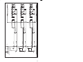
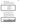
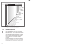
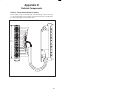
The faceplate of the module contains six LED module status
indicators and a female connector socket. Input signals are brought
into the module via a multiĆconductor cable (M/N 57C372). One end
of this cable has a plug that mates with the faceplate connector
while the other end of the cable has stakeĆon connectors that are
attached to a terminal strip for convenient field wiring connections.
The module's faceplate connector socket and the cable's plug have
provisions for keying the cable to its respective module to prevent
reĆinsertion of the cable into the wrong module.
The six LEDs on the faceplate of the module are shown in figure 2.1.
The first three LEDs are labeled COUNT STOP", LATCH", and
CLEAR". These LEDs correspond to the module's three external
digital inputs. They turn on whenever their corresponding input is
true (high) regardless of whether the input has been enabled on the
module (see register 6).
The next two LEDs are labeled FORWARD" and REVERSE". These
LEDs, when on, indicate whether the counter is counting pulses in
the forward direction or in the reverse direction.
The last LED is labeled CCLK OK". When this LED is on, it indicates
that the constant clock (CCLK) signal is present on the backplane.
2Ć1
COUNT
STOP
LATCH
CLEAR
FORWARD
REVERSE
CCLK
OK
D E
F
C
B
G
Key Slot
NC
A
B
Z
*
FG
A+
*
FG
AB+
*
FG
BZ+
*
FG
Z3
2
1
6
7
8
Key Slot
*FG = Frame Ground (Not Internally Connected)
Figure 2.1 Ć Module Faceplate
2Ć2
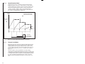
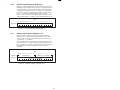
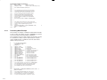
The module contains a pulsetachĆtoĆdigital converter that supplies
data to a 24Ćbit up/down counter. See figure 2.2. The counter counts
up as it follows the pulses received from the pulsetach turning in the
forward direction. It counts down as it follows the pulses received
from the pulsetach in the reverse direction.
Counter
Value
Time
Pulsetach
direction
Stop
Forward
Forward
Stop
Reverse
Figure 2.2 Ć Relationship of Pulsetach Direction to Counter Value
The counter data is latched (i.e., frozen in time) and transferred to
latch registers at userĆspecified intervals. The application program
accesses the counter data through the latch registers.
The module also contains an internal 200 kHz clock that can be
used for timing operations.
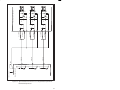
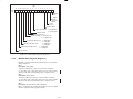
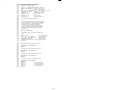
The module's pulsetach input circuitry is shown in figure 2.3.
2Ć3
TO PULSETACH
+5V
TERMINAL
221
681
DIGITAL
FILTER
2
+12V INPUT A
12
+5V INPUT A
14
CHANNEL A
COMMON OR A
TO PULSETACH
+5V
TERMINAL
221
681
DIGITAL
FILTER
3
+12V INPUT B
15
+5V INPUT B
17
CHANNEL B
COMMON OR B
TO PULSETACH
+5V
TERMINAL
221
681
DIGITAL
FILTER
4
+12V INPUT Z
18
+5V INPUT Z
20
CHANNEL Z
COMMON OR Z
Note that all channels are individually isolated.
Figure 2.3 Ć Module Pulsetach Input Circuitry
2Ć4
The module provides three external digital inputs which are enabled
through software (see register 6). Each input causes the module to
perform a specific function at the occurrence of an external signal
on that input as shown below:
D Origin Clear Input Ć Reset the counter
D External Latch Input Ć Read the counter
D External Count Stop Input Ć Stop the counter
The module's digital input circuitry is shown in figure 2.4.
TO EXTERNAL DEVICE
+5V
464
OUT
DIGITAL
FILTER
330
6
ORIGIN
INPUT
7
ORIGIN
COMMON
4.3V
TO EXTERNAL DEVICE
+5V
464
OUT
TERMINAL
DIGITAL
FILTER
330
TERMINAL
8
EXTERNAL
LATCH
INPUT
4.3V
9
EXTERNAL
LATCH
COMMON
TO EXTERNAL DEVICE
+5V
464
OUT
DIGITAL
FILTER
330
TERMINAL
4.3V
Note that all channels are individually isolated.
10
EXTERNAL
COUNT
STOP
INPUT
EXTERNAL
11 COUNT
STOP
COMMON
Figure 2.4 Ć Module Digital Input Circuitry
2Ć5
fafadfdfdasfdsfdsdsdfdsfdsfdsfsdfdsa
afdfdsfdsfdfdsfdsfsadfda
asfdfaddfdd
3.0 INSTALLATION
This section describes how to install and remove the module and its
cable assembly.
CAUTION: The user is responsible for conforming with all applicable local, national,
and international codes. Failure to observe this precaution could result in damage to, or
destruction of, the equipment.
3.1
Wiring
The installation of wiring should conform to all applicable codes.
To reduce the possibility of electrical noise interfering with the
proper operation of the control system, exercise care when installing
the wiring from the system to the external devices. For detailed
recommendations refer to publication IEEE 518.
3.2
Initial Installation
Use the following procedure to install the module:
WARNING
INSERTING OR REMOVING A MODULE OR ITS CONNECTING CABLES MAY
RESULT IN UNEXPECTED MACHINE MOTION. TURN OFF POWER TO THE RACK
BEFORE INSERTING OR REMOVING A MODULE OR ITS CONNECTING CABLES.
FAILURE TO OBSERVE THESE PRECAUTIONS COULD RESULT IN BODILY
INJURY.
Step 1.
Remove power from the system. Power to the rack as
well as all power to the wiring leading to the module
should be off.
Step 2.
Take the module out of its shipping container. Take the
module out of the antiĆstatic bag. Be careful not to touch
the connectors on the back of the module.
Step 3.
Insert the module into the desired slot in the rack. Refer
to figure 3.1. Use a screwdriver to secure the module into
the slot.
Step 4.
Mount the terminal strip (from cable assembly M/N
57C372) on a panel. The terminal strip should be
mounted to allow easy access to the screw terminals. Be
sure the terminal strip is close enough to the rack so that
the cable will reach between the terminal strip and the
module. The cable assembly is approximately 60 inches
long.
3Ć1
16 Slot Rack
16
10 Slot Rack
P/S
0
1
10
2
3
4
5
6
7
8
9
10 11 12 13 14 15
Figure 3.1 Ć Rack Slot Numbers
Step 5.
Attach the pulsetach but leave the mechanical coupling
between the pulsetach and the motor or flowmeter
unconnected.
Fasten the field wires from the pulsetach to the cable
assembly's terminal strip. Typical field connections are
shown in figures 3.2 to 3.5.
Note that 5V openĆcollector inputs require 464 ohm, 1/2
watt pullĆup resistors while 12V openĆcollector inputs
require 1000 ohm, 1/2 watt pullĆup resistors. Also note
that the output openĆcollector transistors in the pulsetach
should have more than 12 mA of current driving
capability.
Use twistedĆpair wire, connected as shown, for the
cabling between the pulsetach and the terminal strip. If
you use wire with less than 2 twists per inch, it should be
shielded. Note that the shield should only be connected
at one end. Ground the cable shield on the module side.
The recommended twistedĆpair wire is Beldent 8761
cable or equivalent.
Cable length should not exceed 600 feet. Maximum
operating cable length for your installation is dependent
upon the type of cable you use and the way the
pulsetach is wired to the module.
Step 6.
Mount the pulsetach's external power supply. The
external power supply should be able to provide either 5 V
at 25 mA plus the pulsetach's power requirements or
12 V at 25 mA plus the pulsetach's power requirements.
Check the specifications of the pulsetach you will be
using.
Fasten the wires from the power supply to the pulsetach.
For best results, the power supply voltage should be
adjusted to provide the specified voltage at the pulsetach.
3Ć2
Step 7.
You may need to add termination resistors to installations
where the twisted pair cable length from the pulsetach to
the module exceeds 200 feet. The resistor value should
be selected dynamically to provide the proper waveform.
See figure 3.2 for typical termination resistor connections.
For 5 VDC inputs, the termination resistors connect
between:
D terminals 12 and 14 (input A)
D terminals 15 and 17 (input B)
D terminals 18 and 20 (input Z).
For 12 VDC inputs, the termination resistors connect
between:
D terminals 2 and 14 (input A)
D terminals 3 and 17 (input B)
D terminals 4 and 20 (input Z).
When a pulsetach is wired for openĆcollector operation,
the termination resistors should be placed as shown in
figure 3.3.
Step 8.
Insert the cable assembly's (M/N 57C372) field terminal
connector into the mating half on the module. Use a
screwdriver to secure the connector to the module.
Note that both the module and the field terminal
connector are equipped with keys" as shown in figure 2.1.
These keys should be used to prevent the wrong cable
from being connected to a module in the event that
connector needs to be removed and then reĆattached
later.
At the time of installation, rotate the keys on the module
and the connector so that they can be connected
together securely. It is recommended that, for modules so
equipped, the keys on each successive module in the
rack be rotated one position to the right of the keys on
the preceding module.
If you use this method, the keys on a particular connector
will be positioned in such a way as to fit together only
with a specific module, and there will be little chance of
the wrong connector being attached to a module.
Step 9.
Check the wiring and be sure all connections are tight.
Step 10.
With the pulsetach disconnected from the motor, apply
power to the rack and the pulsetach. Use an oscilloscope
to test the signal from the pulsetach. The signal at the
terminal strip should be a clean square wave of 5 or 12
volts.
Step 11.
Verify the installation using the Programming Executive
software. Refer to the AutoMax Programming Executive
manual for more information.
Select the I/O Monitor function. For local I/O, enter the
slot number and register number (0Ć7) of the Pulsetach
module. For remote I/O, enter the slot number of the
master Remote I/O module, the remote I/O drop number,
the slot number of the Pulsetach module, and the register
number (0Ć7).
3Ć3
Monitor the counter register and rotate the pulsetach.
Verify that the counter register counts in the proper
direction. If the pulsetach rotates in the wrong direction,
which causes the counter register to count in the wrong
direction, the pulsetach input wires must be switched. In
a singleĆended wiring configuration, swap the A and B
inputs. In a differential wiring configuration, swap the A
and not A inputs.
Step 12.
3.3
Turn off power to the rack and pulsetach. Connect the
mechanical coupling between the motor and the
pulsetach. Turn on power to the system.
Module Replacement
Use the following procedure to replace a module:
WARNING
INSERTING OR REMOVING A MODULE OR ITS CONNECTING CABLES MAY
RESULT IN UNEXPECTED MACHINE MOTION. TURN OFF POWER TO THE RACK
BEFORE INSERTING OR REMOVING A MODULE OR ITS CONNECTING CABLES.
FAILURE TO OBSERVE THESE PRECAUTIONS COULD RESULT IN BODILY
INJURY.
Step 1.
Turn off power to the rack, pulsetachs, and field wiring.
Step 2.
Use a screwdriver to loosen the screws holding the cable
assembly's (M/N 57C372) field wiring connector to the
module. Remove the cable connector from the module.
Step 3.
Loosen the screws that hold the module in the rack.
Remove the module from the slot in the rack.
Step 4.
Place the module in an antiĆstatic bag, being careful not
to touch the connectors on the back of the module. Place
the module in the cardboard shipping container.
Step 5.
Take the new module out of the antiĆstatic bag it came in.
Be careful not to touch the connectors on the back of the
module.
Step 6.
Insert the module into the desired slot in the rack. Use a
screwdriver to secure the module into the slot.
Note that if you are replacing a 57421Ć1 module with a
57C421A or later module, you must add the three
jumpers shown in figure 3.4 to the terminal strip of the
replacement module in order for the module to operate
properly. (Jumper from terminal 14 to terminal 17, and
jumper from terminal 17 to terminal 20.)
If you were using a 57421Ć1 module with 5 V differential
inputs, you must write a zero into bit 11 of register 6. Bit
11 is no longer required to select differential inputs. Bit 11
now selects the polarity of the Z pulse.
3Ć4
Step 7.
Attach the cable assembly's field wiring connector to the
mating half of the connector on the module. Use a
screwdriver to secure the connector to the module.
Step 8.
Turn on power to the rack, the pulsetach, the motor, and
the field wiring.
Figure 3.2 Ć Typical Pulsetach Connections for a 5 or 12 VDC Differential Input
3Ć5
PULSE ENCODER
+12 V or +5 V
VCC
VCC
VCC
SIGNAL Z
SIGNAL Z
Z
SIGNAL B
B
Z
SIGNAL B
SIGNAL A
A
B
SIGNAL A
A
GND
OPTIONAL
TERMINATION
RESISTOR
OPTIONAL
TERMINATION
RESISTOR
OPTIONAL
TERMINATION
RESISTOR
+5 V INPUT
+12 V INPUT
+5 V INPUT
+12 V INPUT
+5 V INPUT
+12 V INPUT
20
18
4
17
15
3
14
12
2
681
681
681
221
221
221
681
681
681
PULSETACH INPUT MODULE
Figure 3.3 ĆTypical Pulsetach Connections for a SingleĆEnded Input with
External PullĆUp Resistor
3Ć6
PULSE ENCODER
+12 V or +5 V
Z
B
A
SIGNAL Z
SIGNAL B
SIGNAL A
GND
+12 V or +5 V
+12 V or +5 V
1K +12 V
464 + 5 V
1K +12 V
464 + 5 V
1K +12 V
464 + 5 V
+5 V INPUT
+12 V INPUT
+5 V INPUT
+12 V INPUT
+5 V INPUT
+12 V INPUT
20
18
4
17
15
3
14
12
2
681
681
681
221
221
221
681
681
681
PULSETACH INPUT MODULE
Figure 3.4 ĆTypical Pulsetach Connections for a SingleĆEnded Input with No
External PullĆUp Resistor
3Ć7
Z
B
A
PULSE ENCODER
+12 V or +5 V
VCC
VCC
VCC
GND
SIGNAL Z
SIGNAL B
SIGNAL A
+5 V INPUT
+12 V INPUT
+5 V INPUT
+12 V INPUT
+5 V INPUT
+12 V INPUT
20
18
4
17
15
3
14
12
2
681
681
681
221
221
221
681
681
681
PULSETACH INPUT MODULE
Figure 3.5 Ć Typical Pulsetach Connections for a Single Channel Input
3Ć8
PULSE ENCODER
+12 or +5 V
SIGNAL A
SIGNAL A
A
A
VCC
GND
OPTIONAL
TERMINATION
RESISTOR
+ 5 V INPUT
+ 12 V INPUT
20
18
4
17
15
3
14
12
2
681
681
681
221
221
221
681
681
681
PULSETACH INPUT MODULE
4.0 PROGRAMMING
This section describes how the data is organized in the module and
provides examples of how the module can be accessed by the
application program.
4.1
Modes of Operation
The module's counter data can be utilized in one of four ways:
D positioning mode
D speed detection mode
D external latch mode
D timer mode
Each mode of operation is described in the following sections. Note
that the speed detection, external catch, and timer modes require
the use of hardware interrupts for proper timing. To use the module
in these modes, the module must be located in a rack containing a
Processor module. Interrupts are not supported in remote racks.
See section 4.5 for more information about using interrupts.
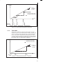
4.1.1
Positioning Mode
Positioning mode is the module's default mode of operation at
power up. In this mode, the counter value is read and transferred to
the latch registers whenever the application program requests
counter data. The latch registers hold this value until the next data
request is received. The counter is not automatically reset when it is
read. See figure 4.1.
Counter
Value
Ċ Internal Counter Value
Latched Counter Value
Time
APPLICATION PROGRAM DATA REQUESTS
Figure 4.1 Ć Counter Status During Positioning Mode
4Ć1
4.1.2
Speed Detection Mode
Speed detection mode is enabled by setting the Timer Interrupt
Enable bit (register 5, bit 5) to 1. In this mode, the counter value is
read and transferred to the latch registers each time the time period
defined in the Update Register (register 2) expires. Each time the
counter is read, the counter is reset to zero and an interrupt is
generated. The latch registers hold the latched counter value until
the counter is read again. Refer to figure 4.2.
Counter
Value
Ċ Internal Counter Value
Latched Counter Value
Decreasing
Speed
Time
Constant
Time Intervals
(Programmable)
Figure 4.2 Ć Counter Status During Speed Detection Mode
4.1.3
External Latch Mode
External latch mode is enabled by setting the Enable External Latch
Input bit (register 6, bit 0) to one. In this mode, the counter value is
read and transferred to the latch registers at the occurrence of an
external signal on the input connected to terminal 8. This signal can
be from a push button, photoĆsensor, or a similar device. Refer to
figure 4.3.
The latch registers can be programmed to be either leading
edgeĆtriggered or trailing edgeĆtriggered. The status of register 6, bit
14 (External Latch Input Select) defines when the external latch input
is considered to be true. The counter is not automatically reset when
it is read. To generate an interrupt when the counter is read, the
External Latch Interrupt Enable bit (register 5, bit 8) must be set to
one.
4Ć2
Counter
Value
Slope is
constant at
200 kHz
Ċ Internal Counter Value
Latched Counter Value
Time
External
Latch Input
Figure 4.3 Ć Counter Status During External Latch Mode
Timer mode is enabled by setting the Timer/Counter Select bit
(register 5, bit 13) to one. In this mode, the module's 200 kHz clock
serves as a pulse generator which provides constant and uniform
pulses to the counter's input. When the input pulses are used in
conjunction with the external latch signals, the time interval between
two events can be measured. No external wiring is needed to use
the 200 kHz clock as a counter input. See figure 4.4.
Counter
Value
Ċ Internal Counter Value
Latched Counter Value
Slope is
constant at
200 kHz
Time
External
Latch
Figure 4.4 Ć Counter Status During Timer Mode
4Ć3
4.2
Register Organization
The module contains registers for the pulse counter, the comparator,
the timer, module status, and module control. The register
organization is shown in figure 4.5. The following sections describe
each register in detail. A detailed memory map can be found in
Appendix G. Note that at power up, all registers are cleared (reset to
zero).
Register
0
1
2
3
4
5
6
7
Description
Counter Data Latch Register
Counter Data Latch Register
Counter Update Register
Comparator Register
Comparator Register
Interrupt Status and Control Register
Mode Definition Register
Module Status Register
Figure 4.5 Ć Pulsetach Module Register Organization
4.2.1
Counter Data Latch Registers (Registers 0Ć1)
Registers 0 and 1 contain a latched copy of the contents of the
module's 24Ćbit signed counter. Refer to figure 4.6.
The largest value that the counter can hold is +/- 8,388,607. This
information can be accessed by referencing registers 0 and 1 as a
long integer or as an integer by referencing register 1. Bit 7 of
register 0 is the sign bit. Bits 8 to 15 are always set to the state of bit
7. Reference the counter as an integer (register 1) if the counter
value will not exceed 32767 between readings. If the counter value
will exceed 32767, reference the counter as a long integer. These
registers are readĆonly.
Bits
15 14 13 12 11 10
Register 0
Register 1
extended sign
9
8
7
6
5
4
3
LS 16 bits of counter
Figure 4.6 Ć Counter Data Latch Registers (Registers 0Ć1)
4Ć4
2
1
MS 8 bits of counter
0
4.2.2
Counter Update Register (Register 2)
Register 2 contains the update period for reading the counter and
updating the latch registers. Refer to figure 4.7. The update period is
equal to the value in register 2 plus one. Each count in this register
is equivalent to 500 microseconds. For example, if you want data
latched every 22 msec., assign register 2 a value of 43 ([22 msec/.5
msec] - 1 = 43). The update period may range from 500
microseconds to 32.768 seconds. This register is read/write and is
enabled whenever bit 5, of register 5 (Timer Interrupt Enable), is set.
15 14 13 12 11 10
Register 2
9
Bits
8 7
6
5
4
3
2
1
0
update period
Figure 4.7 Ć Counter Update Register (Register 2)
4.2.3
Comparator Registers (Registers 3Ć4)
Registers 3 and 4 contain a 24Ćbit signed comparator. Refer to
figure 4.8. Bit 7 of register 3 is the sign bit. Bits 8 to 15 are always
set to the state of bit 7. The largest value that can be stored in the
comparator is +/- 8,388,607.
This information can be accessed by referencing registers 3 and 4
as a long integer or as a simple integer by referencing register 4. If
the comparator is referenced as a simple integer, it can contain only
positive numbers less than or equal to 32767. This register is
read/write.
Bits
15 14 13 12 11 10
Register 3
Register 4
extended sign
9
8
7
6
5
4
3
2
1
0
MS 8 bits of comparator
LS 16 bits of comparator
Figure 4.8 Ć Comparator Registers (Registers 3Ć4)
4Ć5
4.2.4
Interrupt Status Control Register (Register 5)
The bits in register 5 are used to enable interrupts and define other
module characteristics. This register is read/write. Refer to figure 4.9.
WARNING
BITS 0, 1, 2, 7, AND 15 ARE CONTROLLED BY THE OPERATING SYSTEM AND
MUST NOT BE WRITTEN TO BY THE USER. WRITING TO THESE BITS MAY
RESULT IN ALL OUTPUTS BEING TURNED OFF AND ALL TASKS IN THE RACK
BEING STOPPED. FAILURE TO OBSERVE THESE PRECAUTIONS COULD
RESULT IN BODILY INJURY.
Bit: 0
Description: System use only.
Bit: 1
Description: System use only.
Bit: 2
Description: System use only.
Bits: 3 and 4
Description: Counter Clear Control
These bits are used to define the conditions under which the
counter is reset to zero.
Bit 4
Condition
Bit 3
0
0
1
1
0
1
0
1
Never clear (1)
External latch (2)
Counter equal comparator
After counter is read (3)
(1) Bit 14 of this register must also be set to one.
(2) The external latch input must also be enabled (register 6, bit 0).
(3) This feature is not available in external latch mode (i.e., register
6, bit 0 = 1).
NOTE: ! ! ! ! # ! ! " ! ! Bit: 5
Description: Timer Interrupt Enable
When this bit is equal to one (i.e., speed detection mode), the
counter data is latched, an interrupt is generated, and the counter is
reset each time the time period specified in register 2 (Counter
Update Register) expires. (Note that if bit 14 is also set to one, the
counter will not be cleared after an interrupt.)
If the status of bit 5 is changed to zero after the module has been
operating in the speed detection mode, the counter data will be
latched when bit 5 makes the transition from one to zero and the
counter will not be reset.
Bit: 6
Description: Generate CCLK
When this bit is set to one, the module will provide the CCLK signal
to the rack backplane. The CCLK signal can be generated by this
module, an Analog Input module (M/N 57C409), a Resolver Input
4Ć6
module (M/N 57C411), or a Universal Drive Controller module
(B/M OĆ57552 or OĆ57652). Only one module per rack may provide
the CCLK signal.
If the Pulsetach Input module does not detect the CCLK signal on
the backplane, it will use its own internal clock. (Under this
condition, the CCLK OK LED on the module faceplate will be off.)
Note that if the rack contains more than one module that can
generate the CCLK signal, the backplane CCLK signal must be
turned on by one of the modules in order to synchronize the
modules.
7
System use only.
8
External Latch Interrupt Enable
When this bit is set to one, an interrupt is generated when the
transition specified in register 6, bit 14 (External Latch Input Select)
occurs. When an external latch interrupt occurs, you must reset the
interrupt by writing a zero to register 7, bit 13 (External Latch Status
Reset).
9
External Count Stop Interrupt Enable
When this bit is set to one, an interrupt is generated when the
condition specified in register 6, bit 12 (Count Stop Input Select)
occurs. When an external count stop interrupt occurs, you must
reset the interrupt by writing a zero to register 7, bit 14 (External
Count Stop Status Reset). Note that the Inhibit Counter bit (register
6, bit 9) is also set internally by the module when an external count
stop interrupt occurs and must be reset after each interrupt to
enable the module to count again.
10
Z Pulse and Origin Interrupt Enable
When this bit is set to one, an interrupt is generated whenever the Z
Pulse and origin clear input signals are activated. Note that the
Origin/Clear Status bit (register 6, bit 10) must be set to 0. When a Z
pulse and origin interrupt occurs, you must reset the interrupt by
writing a zero to register 7, bit 15 (External Origin/Clear Status
Reset). For additional information, refer to register 6, bit 10.
11
Comparator Equal Interrupt Enable
When this bit is set to one, an interrupt is generated when the
counter value equals the comparator value as indicated in register 7,
bit 4 (Counter Equals Comparator Status). When a comparator
equal interrupt occurs, you must reset the interrupt by writing a zero
to register 7, bit 12.
You must set the comparator value before you enable the
comparator equal interrupt (register 5 bit 11).
Note that if you do not set the comparator value before you enable
the interrupt at power up (when all internal registers are equal to
zero), a comparator equal interrupt will be issued and error 1b" will
be displayed on the faceplate of the Processor.
12
Pulse Multiplier
This bit specifies how the incoming pulses from a quadrature pulse
tach are multiplied. If the bit is set to one, the incoming frequency is
4Ć7
multiplied by four. If the bit is set to zero, the incoming pulses are
multiplied by two.
If a singleĆchannel pulsetach is connected to the module, this bit
should be set to zero. Incoming pulses from a singleĆchannel
pulsetach are not multiplied.
13
Timer/Counter Select
When this bit is set to one, the module functions as a timer using its
internal 200 kHz clock (no external cabling from the pulsetach is
required). If the bit is set to zero, the module functions as counter
based on pulsetach inputs.
14
Counter Clear Inhibit
When this bit is set to one, the counter will not be cleared after an
interrupt while the module is operating in speed detection mode.
Note that bits 3 and 4 of this register must both be set to zero to
activate this feature. When this bit is set to zero, the module will
operate in speed detection mode as described in section 4.1.2; i.e.,
the counter will be cleared after each interrupt.
15
System use only.
15 14 13 12 11 10
Register 5
9
Bits
8 7
rw rw rw rw rw rw rw
6
5
4
3
2
1
0
rw rw rw rw
Counter clear control
00: Never clear the
counter
01: External latch
10: Comparator equal
11: After counter read
Timer interrupt enable
Generate CCLK
External latch interrupt enable
External count stop interrupt enable
Z pulse and origin interrupt enable
Comparator equal interrupt enable
Pulse multiplier
Timer/counter select
0: Counter
1: Timer
Counter clear inhibit
Figure 4.9 Ć Interrupt Status Control Register (Register 5)
4Ć8
4.2.5
Mode Definition Register (Register 6)
Register 6 is a control register used to define the module's operating
mode. Refer to figure 4.10. This register is read/write.
WARNING
BITS 4, 5, 6, AND 7 ARE CONTROLLED BY THE OPERATING SYSTEM AND MUST
NOT BE WRITTEN TO BY THE USER. WRITING TO THESE BITS MAY RESULT IN
ALL OUT PUTS BEING TURNED OFF AND ALL TASKS IN THE RACK BEING
STOPPED. FAILURE TO OBSERVE THESE PRECAUTIONS COULD RESULT IN
BODILY INJURY.
Bit: 0
Description: External Latch Enable
Bit 0 is used to enable the external latch input. When this bit is set to
one and the external latch input makes the transition specified by
register 6, bit 14, the value in the counter at that time will be stored
in registers 0 and 1.
Bit: 1
Description: External Count Stop Enable
Bit 1 is used to enable the external count stop input. When this bit is
set to one and the external count stop input is equal to the condition
specified by register 6, bit 12, the counter will stop counting.
Bits: 2 and 3
Description: Count Reverse and Count Forward
Bits 2 and 3 are used to define the counter direction when the
clear/origin input is used to initialize the absolute position of an
external device. When the clear/origin input is used for this purpose,
you must define whether the counter should be counting forward or
backward when the marker pulse resets the counter. Refer to
register 6, bit 10 for more information.
Set bit 2 to one if the counter should be counting in the reverse
direction. Set bit 3 to one if the counter should be counting in the
forward direction.
Bit: 4
Description: System use only.
Bit: 5
Description: System use only.
Bit: 6
Description: System use only.
Bit: 7
Description: System use only.
Bit: 8
Description: Type of Pulsetach
Bit 8 defines the type of pulsetach connected to the module. This bit
should be set to zero if a quadrature (A and B) pulsetach is
connected. A quadrature pulsetach is required to count forward and
reverse pulses.
This bit should be set to one if a singleĆinput pulsetach is
connected. A singleĆinput pulsetach may be connected to either the
A or B inputs. Note that with a singleĆinput pulsetach, the counter
4Ć9
will always count up; however, the FORWARD and REVERSE LEDs
will flicker.
9
Inhibit Counter
Bit 9 is used to stop the counter from counting. When this bit is set
to one, the counter will not count incoming pulses. Note that this bit
is also set internally by the module when an external count stop
interrupt occurs (see register 5, bit 9). This bit must be reset after an
external count interrupt is generated to enable the module to count
again.
10
Origin/Clear Select
Bit 10 is used to specify the action that occurs when the origin/clear
input is true. If bit 10 is equal to one, the origin/clear input will reset
the counter whenever it is in the same state as the value specified
by register 6, bit 13. If bit 10 is equal to zero, the counter will be
reset when: the origin/clear input is in the same state as the value
specified by register 6, bit 13, the counter is counting in the direction
specified by register 6, bits 2 or 3, and the marker (Z) pulse occurs.
The latter is typically used to initialize the absolute position of a
machine.
11
Z Pulse Polarity
Bit 11 is used to specify the polarity of the Z pulse. If bit 11 is zero
(default), the Z pulse's logic is positive. If bit 11 is one, the pulse's
logic is negative.
12
Count Stop Input Select
Bit 12 is used to specify when the count stop input is considered to
be true. If this bit is zero, a high input signal (+V) will be considered
to be true. If this bit is one, a low input signal (0V) will be considered
to be true.
13
Origin/Clear Input Select
Bit 13 is used to specify when the origin/clear input is considered to
be true. If this bit is zero, a high input signal (+V) will be considered
to be true. If this bit is one, a low input signal (0V) will be considered
to be true.
14
External Latch Input Select
Bit 14 is used to specify when the external latch input is considered
to be true. If this bit is zero, a high input signal (+V) will be
considered to be true. If this bit is one, a low input signal (0V) will be
considered to be true.
15
Reset Counter
Bit 15 is used to reset the 24Ćbit counter under software control. The
counter is reset to zero whenever this bit is set.
4Ć10
Bits
15 14 13 12 11 10
9
8
7
6
RegisĆ rw rw rw rw rw rw rw rw
ter 6
5
4
3
2
1
0
rw rw rw rw
External
latch
enable
External
count stop
enable
Count
reverse
Count forward
Type of pulsetach: 0 = quadrature
1 = single input
Inhibit counter
Clear/origin select
Z pulse polarity: 0 = positive logic
1 = negative logic
Count stop input select: 0 = high input
1 = low input
Origin/clear input select:
External latch input select:
Reset counter
0 = high input
1 = low input
0 = high input
1 = low input
Figure 4.10 Ć Mode Definition Register (Register 6)
4.2.6
Module Status Register (Register 7)
Register 7 contains module status and interrupt reset control bits.
Refer to figure 4.11.
Bit: 0
Description: Carry Status
This bit is set whenever a carry occurs from bit 7 of register 0
(i.e., the value of the counter has rolled over to zero in the positive
direction). This bit is reset by writing a zero to register 7, bit 10.
Bit: 1
Description: Borrow Status
This bit is set whenever a borrow occurs from bit 7 of register 0
(i.e., the value of the counter has rolled over to zero in the negative
direction). This bit is reset by writing a zero to register 7, bit 11.
Bit: 2
Description: Counter Greater Than Comparator
Bit 2 is set whenever the counter value (registers 0 and 1) is greater
than the comparator value (registers 3 and 4).
4Ć11
3
Counter Less Than Comparator
Bit 3 is set whenever the counter value (registers 0 and 1) is less
than the comparator value (registers 3 and 4).
4
Counter Equals Comparator
Bit 4 is set whenever the counter value (registers 0 and 1) is equal to
the comparator value (registers 3 and 4). This bit can be reset by
writing a zero to register 7, bit 12.
5
External Latch Input Status
Bit 5 contains the status of the external latch. This bit is set and
latched whenever the external latch makes the transition specified
by register 6, bit 14. Note that this bit will contain status data only if
the External Latch Enable bit (register 6, bit 0) is set. This bit is reset
by writing a zero to register 7, bit 13.
6
External Count Stop Internal Status
Bit 6 is set and latched whenever the external count stop input is
equal to one. Note that this bit will contain status information only if
the External Count Stop Enable bit (register 6, bit 1) is set. This bit is
reset by writing a zero to register 7, bit 14.
7
Origin/Clear Input Status
Bit 7 contains the status of the external origin/clear input. This bit is
set whenever the external origin/clear input is true. This bit can be
reset by writing a zero to register 7, bit 15.
8
CCLK Off
Bit 8 indicates that the CCLK signal on the backplane is off. This
signal can be generated by this module (register 5, bit 6), an Analog
Input module (M/N 57C409), a Resolver Input module (M/N 57C411)
or a Universal Drive Controller module (B/M OĆ57552 or OĆ57652).
Only one module per rack may control the CCLK signal.
If the module does not detect the CCLK signal on the backplane, it
will use its own internal clock. (Under this condition, the CCLK OK
LED on the module faceplate will be off.) However, if the rack
contains more than one module that can generate the CCLK signal,
the backplane CCLK signal must be turned on in order to
synchronize the modules.
9
Pulse Input Direction
Bit 9 contains the direction of the last count read in by the counter.
The counter's direction can be either forward (0) or reverse (1).
10
Carry Status Reset
Bit 10 has a default value of one. Writing a zero to this bit will reset
the Carry Status bit (register 7, bit 0), but subsequent reads will
return a value of one.
4Ć12
11
Borrow Status Reset
Bit 11 has a default value of one. Writing a zero to this bit will reset
the Borrow Status bit (register 7, bit 1), but subsequent reads will
return a value of one.
12
Counter Equals Comparator Status Reset
Bit 12 has a default value of one. Writing a zero to this bit will reset
the Counter Equals Comparator Status bit (register 7, bit 4) and the
comparator equal interrupt (see register 5, bit 11), but subsequent
reads will return a value of one.
13
External Latch Status Reset
Bit 13 has a default value of one. Writing a zero to this bit will reset
the External Latch Status bit (register 7, bit 5) and the external latch
interrupt (see register 5, bit 8), but subsequent reads will return a
value of one.
14
External Count Stop Status Reset
Bit 14 has a default value of one. Writing a zero to this bit will reset
the External Count Stop Status bit (register 7, bit 6) and the external
count stop interrupt (see register 5, bit 9), but subsequent reads will
return a value of one. Note that the Inhibit Counter bit (register 6, bit
9) also must be reset after an external count stop interrupt is
generated.
15
External Origin/Clear Status Reset
Bit 15 has a default value of one. Writing a zero to this bit will reset
the External Origin/Clear Status bit (register 7, bit 7) and the Z pulse
and origin interrupt (see register 5, bit 10), but subsequent reads will
return a value of one.
4Ć13
15 14 13 12 11 10
9
Bits
8 7
6
5
4
3
2
1
0
Register 7 rw rw rw rw rw rw
r
r
r
r
r
r
r
r
r
r
Carry
status
Borrow
status
Counter >
comparator
Counter <
comparator
Counter =
comparator status
External latch
input status
External count stop
input status
Origin/clear input status
CCLK off
Pulse input direction: 0 = Forward
1 = Reverse
Carry status reset
Borrow status reset
Counter = comparator status reset
External latch status reset
External count stop status reset
External origin/clear status reset
Figure 4.11 Ć Module Status Register (Register 7)
4.3
Variable Configuration
Before an application task can be written, you need to configure, or
define, systemĆwide data such as the registers on the Pulsetach
Input module as variables. These are variables that must be globally
accessible to more than one task in the rack.
For DCS 5000 and AutoMax Version 2.1 and earlier, you define
systemĆwide variables by writing a Configuration task. For AutoMax
Version 3.0 and later, you define systemĆwide variables using the
AutoMax Programming Executive configuration forms. After the
variables are defined, you can generate the configuration file
automatically.
If you are using AutoMax Version 2.1 or earlier, refer to Appendix F
for examples that show how to define variables in the configuration
task. If you are using AutoMax Version 3.0 or later, see the AutoMax
Programming Executive for information about configuring variables.
4Ć14
4.4
Applying the Module
In order for hardware to be referenced by application software, it is
first necessary to assign symbolic names to the hardware. This is
accomplished in the configuration, as described in the section 4.3.
Each task that wishes to reference the symbolic names assigned to
the Pulsetach Input module may do so by declaring those names
COMMON. Once this has been done, any reference to those
symbolic names within the task will reference the bit or register
defined in the configurations.
The frequency with which tasks read input variables and write output
variables depends on the programming language being used.
Ladder Logic and Control Block tasks read all their inputs once at
the beginning of each scan, regardless of how often the inputs are
referenced in the task and write all output variables at the end of the
scan. BASIC statements (even within Control Block tasks) read an
input each time it is referenced and write an output each time it is
referenced.
4.4.1
Speed Mode Example
The following is an example of a Control Block task that handles
interrupts from the module. All variables declared as COMMON are
assumed to be previously been defined during configuration.
In the example below, the module is continuously accumulating
pulses from a pulsetach. The module is set up to capture the value
of the counter at a periodic rate and then generate an interrupt. This
task could be used to read in counts and then accumulate them in
software. It could also be used to generate a velocity signal (dx/dt).
1
2
3
4
5
1000
1005
1010
1015
1020
1025
1200
2100
2200
2201
2202
2203
2204
3000
3001
3002
3003
3004
3005
3006
3007
3008
3009
3010
4000
4001
4002
4003
4004
4005
4100
!ă
!ăSPEED MODE EXAMPLE
!ăTASK NAME : PG_SPEED
!ăPRIORITY : 5
!ă
COMMON TIMER%
\!Counter read time
COMMON ISCR%
\!Interrupt and status register
COMMON COUNT%
\!Counter data
COMMON MULT@
\!Pulse multiplier
COMMON CCLK_EN@
\!CCLK enable
COMMON INT_R@
\! Timer interrupt enable
LOCAL COUNTER_VALUE% \!Counter value from buffer
MULT@ = ON
\!Pulse multiplier times 4
TIMER% = 99
\!Read every 50 milliseconds
!
! Set all other timers in the rack here.
! (To be done in only 1 task in a rack.)
!
!ă
!ăThe following statement connects the name COUNTER_EVENT
!ăto the interrupt defined in ISCR%. The event name should
!ăbe as descriptive as possible. The watchdog timeout has
!ăbeen set to 12 Processor clock ticks (12*5.5 secs). If the time
!ăbetween interrupts exceeds this value, a severe error
!ăwill be declared and the system will be stopped. For
!ă
!ă
!ă
EVENT NAME=COUNTER_EVENT, INTERRUPT_STATUS=ISCR%,
TIMEOUT=12
!ă
!ăThe following statement enables the constant clock" from
!ăthis module. If there is more than one interrupt task in a
!ăchassis, the task that enables the constant clock" should
!ăalways be the lowest priority task.
!ă
DIS_CRL@=FALSE
\!Counter will be reset on interrupt.
4Ć15
Speed Mode Example (Continued)
4105
4110
5000
5001
5002
6000
6001
6002
6003
6004
6005
6006
6007
6008
6010
7000
7001
7002
7003
7004
7005
7006
10000
32767
4.4.2
INT_R@ = TRUE
\! Enable timer interrupt
CCLK_EN@ = TRUE
\! Enable CCLK (1 CCLK driver per rack)
!
!ăPlace additional initialization software here.
!ă
!ă
!ăThe next statment synchronizes the task to the external
!ăevent via the interrupt. Task execution will be suspended
!ăuntil the interrupt occurs. When the interrupt occurs, if
!ăthis task is the highest priority task waiting to execute,
!ăit will become active. If it is not the highest priority
!ătask, it will remain suspended until all higher priority
!ătasks have finished executing at which point it will then
!ăbecome active.
CALL SCAN_LOOP( TICKS=9, EVENT=COUNTER_EVENT )
!ă
!
!
!ăThis example assumes that 32767 or fewer counts will be
!ăreceived in the 50 msec. scan because statement 10000 only
!ăreferences the least significant register (1) on the
!ăregister.
CALL PULSE_MULT( INPUT= COUNT%, MULTIPLIER= 16385, ăăăăăăăăăăă&
OUTPUT= COUNTER_VALUE% )
END
Positioning Mode Example
The following is an example of a BASIC task that handles interrupts
from the module. All variables declared as COMMON are assumed
to have previously been defined during configuration.
In the example below, the module generates an interrupt every time
it accumulates the number of pulses indicated by the compare
register. Additional tasks or additional code in this task must be
written to take specific action.
1
2
3
4
5
1000
1005
1010
1015
1020
1025
1030
1035
1040
1200
1205
1210
1215
1220
1225
1230
3000
3001
3002
3003
3004
3005
3006
3007
3010
4000
4001
4002
4003
4004
4Ć16
!ă
!ăPOSITIONING MODE EXAMPLE
!ăTASK NAME: PG_COMP
!ăPRIORITY: 10
!
COMMON COUNT%
\!ăCounter data
COMMON LOW_COMP%
\!ăComparator data
COMMON ISCR%
\!ăInterrupt status and control
COMMON RESET@
\!ăCounter reset
COMMON CNTR_EQ_RST@ \!ăComparator equal interrupt reset
COMMON EQU_INT@
\! Comparator equal int. enable
COMMON CLR_MOD1@
\! Counter clear condition
COMMON CLR_MOD2@
\! Counter clear condition
COMMON CCLK_EN@
\!
LOCAL LIMIT_SWITCH%(3)
\!ăTable of limit switch positions
LOCAL INDEX%
\!ăIndex of limit switch interrupt
LOCAL I%
\!ăIndex of next limit switch interrupt
LOCAL INT_SERVICE0%
\!ăCounter for interrupt service 0
LOCAL INT_SERVICE1%
\!ăCounter for interrupt service 1
LOCAL INT_SERVICE2%
\!ăCounter for interrupt service 2
LOCAL INT_SERVICE3%
\!ăCounter for interrupt service 3
!
!ăThe following statement connects the name COUNTER_EVENT
!ăto the interrupt defined in ISCR%. The event name should
!ăbe as descriptive as possible. The watchdog timeout has
!ăbeen disabled because the event is not periodic.
!ă
!ă
!ă
EVENT NAME=COUNTER_EVENT, INTERRUPT_STATUS=ISCR%, &
TIMEOUT=DISABLED
!
!ăThe following statements initialize the counter and set
!ăup the interrupt control. Constant clock" is enabled on
!ăthis module. If there is more than one interrupt task in
!ăa chassis, the task that enables constant clock" should
Positioning Mode Example (Continued)
4005
4006
4010
4015
4020
4025
4030
4035
4040
4045
4050
5988
5989
5990
5991
5992
5993
5994
5995
5996
5997
5998
5999
6000
6010
6997
6998
6999
7000
7010
7015
7020
7025
7030
7035
7997
7998
7999
8000
8190
8197
8198
8199
8200
8390
8397
8398
8399
8400
8590
8597
8598
8599
8600
8790
9000
9005
9010
9020
32767
!ăalways be the lowest priority task.
!
FOR I% = 0 TO 3 \ READ LIMIT_SWITCH%(I%) \ NEXT I%
RESET@ = TRUE \ RESET@ = FALSE
\!ăZero counter
I% = 0
\!ăInitialize limit switch index
LOW_COMP% = LIMIT_SWITCH%(I%)
\!Set comparator to 1st value
CNTR_EQ_RST@ = FALSE
\!ăInitialize 'Comp=' status
EQU_INT@ = ON
\! Enable comp = interrupt
CLR_MOD1@ = OFF
\! Reset on equal
CLR_MOD2@= ON
\! Reset on equal
CCLK_EN@ = ON
\! Enable constant clock
!
!ăPlace additional initialization software here.
!
!
!ăThe next statement synchronizes the task to the external
!ăevent via the interrupt. Task execution will be suspended
!ăuntil the interrupt occurs. When the interrupt occurs, if
!ăthis task is the highest priority task waiting to
!ăexecute, it will become active. If it is not the highest
!ăpriority task, it will remain suspended until all higher
!ăpriority tasks have executed at which point it will then
!ăbecome active.
!
WAIT ON COUNTER_EVENT
!
!ăThe following statements perform the interrupt service
!ăroutine.
!
INDEX% = I% + 1
\!ăSave this index value
I% = I% + 1 \ IF I% > 3 THEN I% = 0
\!ăStep to next point
LOW_COMP% = LIMIT_SWITCH%( I% ) \!ăSet up next value
CNTR_EQ_RST@ = FALSE
\!ăReset interrupt
ON INDEX% GOSUB 8000, 8200, 8400, 8600 \ !Execute routine
GOTO 6010
!
!ăInterrupt service routine for limit switch value (0).
!
INT_SERVICE0% = INT_SERVICE0% + 1
RETURN
!
!ăInterrupt service routine for limit switch value (1).
!
INT_SERVICE1% = INT_SERVICE1% + 1
RETURN
!
!ăInterrupt service routine for limit switch value (2).
!
INT_SERVICE2% = INT_SERVICE2% + 1
RETURN
!
!ăInterrupt service routine for limit switch value (3).
!
INT_SERVICE3% = INT_SERVICE3% + 1
RETURN
DATA 1000
\!ăLimit switch position 0
DATA 500
\!ăLimit switch position 1
DATA 2500
\!ăLimit switch position 2
DATA 3000
\!ăLimit switch position 3
END
4Ć17
4.4.3
Timer and Latch Mode Example
The following is an example of a BASIC task that handles interrupts
from the module. All variables declared as COMMON are assumed
to have previously been defined during configuration.
In the example below, the task counts pulses generated by the
internal 200 kHz clock. Each time an external latch input signal is
received, the task latches the counter data and then clears the
counter.
1
2
3
4
5
1000
1005
1010
1015
1020
1025
1030
1035
1040
1045
1050
1200
3000
3001
3002
3003
3004
3005
3006
3007
3010
4000
4001
4002
4003
4004
4005
4006
4010
4015
4020
4025
4030
4035
4040
4045
5988
5989
5990
5991
5992
5993
5994
5995
5996
5997
5998
5999
6000
6997
6998
6999
7000
7005
7010
32767
4Ć18
!ă
!ăTIMER AND EXTERNAL LATCH MODE EXAMPLE
!ăTASK NAME: PG_LATCH
!ăPRIORITY: 10
!ă
COMMON COUNT%
\!ăCounter data
COMMON ISCR%
\!ăInterrupt status & control
COMMON RESET@
\!ăCounter reset
COMMON EXT_LATCH_EN@ \!ăExternal latch enable
COMMON LATCH_POLARITY@ \!ăExternal latch polarity
COMMON LATCH_RESET@
\!ăExternal latch interrupt reset
COMMON TIM_MOD@
COMMON LAT_INT@
COMMON CCLK_EN@
COMMON CLR_MOD1@
COMMON CLR_MOD2@
LOCAL DELTA%
\!ăTime between external events
!ă
!ăThe following statement connects the name COUNTER_EVENT
!ăto the interrupt defined in ISCR%. The event name should
!ăbe as descriptive as possible. The watchdog timeout has
!ăbeen disabled because the event is not periodic.
!ă
!ă
!ă
EVENT NAME=COUNTER_EVENT, INTERRUPT_STATUS=ISCR% ă ă&
TIMEOUT=DISABLED
!
!ăThe following statements initialize the counter and set
!ăup the interrupt control. Constant clock" is enabled on
!ăthis module. If there is more than one interrupt task in
!ăa chassis, the task that enables constant clock" should
!ăalways be the lowest priority task.
!ă
RESET@ = TRUE \ RESET@ = FALSE \!ăZero counter
EXT_LATCH_EN@ = TRUE
\!ăEnable the external latch
LATCH_POLARITY@ = FALSE \!ăLatch input is high true
TIM_MOD@ = ON
\! Timer mode
LAT_INT@ = ON
\! External latch int. enable
CLR_MOD1@ = OFF
\! Clear counter after
CLR_MOD2@ = ON
\! External latch
CCLK_EN@ = ON
\! Enable CCLK
!
!ăPlace additional initialization software here.
!
!ă
!ăThe next statement synchronizes the task to the occurence
!ăof the external latch via the interrupt. Task execution
!ăwill be suspended until the interrupt occurs. When the
!ăinterrupt occurs, if this task is the highest priority
!ătask waiting to execute, it will become active. If it is
!ănot the highest priority task, it will remain suspended
!ăuntil all other higher priority tasks have been executed
!ăat which point it will then become active.
WAIT ON COUNTER_EVENT
!
!ăThe following statements perform the interrupt service
!ăroutine.
DELTA% = COUNT%
\!ăRead time between external events
LATCH_RESET@ = FALSE
\!ăReset the interrupt
GOTO 6000
\!ăWait for the next event
END
4.5
Using Interrupts in Application Tasks
The input module can be programmed to generate interrupts on the
basis of a time interval, an external latch input, an external count
stop input, a marker pulse and origin input, or a comparator equal
condition. Time intervalĆbased interrupts cannot be used with any
other interrupts.
Interrupts are used to synchronize software tasks to the occurrence
of a hardware event. This module provides the ability to synchronize
events beginning at 1.2 msec and increasing in increments of
500 msec depending on the priority level of the task receiving the
interrupt.
In order to use interrupts on the Pulsetach Input module, the module
must be in a rack containing a Processor module. Interrupts cannot
be used with Pulsetach Input modules located in remote racks.
You must first assign symbolic names to the interrupt control
registers on the module during configuration. Only one task may act
as the receiver for the interrupts generated by a Pulsetach Input
module. That task should declare the symbolic names assigned to
the interrupt control registers as COMMON. The Interrupt Status and
Control register (register 5) must be referenced in the hardware
EVENT statement in the task receiving the interrupt. The examples in
sections 4.4.1, 4.4.2, and 4.4.3 illustrate various uses of the interrupt
feature. Note that the receiving task uses either the SCAN_LOOP
(Control Block) statement or the WAIT ON (BASIC) statement to
actually receive the signal. (Refer to the Control Block and BASIC
Language instruction manuals.)
All interrupts are internally doubleĆbuffered. This helps to eliminate
spurious interrupts, which could cause system errors when the
module is operated in an electrically noisy environment. The
application task must provide a tightlyĆcoupled software handshake
with the external asynchronous interrupt inputs coming into the
module. Register 7, the Module Status register, is used in this
handshaking. The status bits in register 7 are set to one when an
interrupt input is received and remain set until the application
program clears them. As long as the status bits in the register are
equal to one, the module will not recognize additional interrupt
inputs as they occur.
4.6
Restrictions
This section describes limitations and restrictions on the use of the
Pulsetach Input module.
4.6.1
Writing Data to Registers
The module's counter registers (registers 0 and 1) are read only.
Attempts to write to them will cause a Bus Error (STOP ALL system
error indicated by a 31" on the faceplate of the Processor).
Some examples of programs that write to the module and must not
be used are:
D Referencing an input on the left side of an equal sign in a Control
Block or BASIC task.
D Referencing an input as an output in a Control Block function.
4Ć19
4.6.2
Use in Remote I/O Racks
32Ćbit register references should be used with caution when this
module is placed in a remote rack. The remote I/O system does not
always transfer registers greater than 16 bits as a unit. As a result, it
is possible for an application task to read the least significant 16 bits
of a new value and the most significant 16 bits of the previous value.
Interrupts cannot be used with Pulsetach Input modules in remote
racks.
WARNING
IF YOU USE DOUBLE INTEGER VARIABLES IN THIS INSTANCE, YOU MUST
IMPLEMENT A SOFTWARE HANDSHAKE BETWEEN THE TRANSMITTER AND
THE RECEIVER TO ENSURE THAT BOTH THE LEAST SIGNIFICANT AND MOST
SIGNIFICANT 16 BITS HAVE BEEN TRANSMITTED BEFORE THEY ARE READ BY
THE RECEIVING APPLICATION PROGRAM. FAILURE TO OBSERVE THIS
PRECAUTION COULD RESULT IN BODILY INJURY OR DAMAGE TO EQUIPMENT.
4.6.3
Pulsetach Feedback Precautions
WARNING
LOSS OF, OR AN OTHERWISE IMPROPER, PULSETACH SIGNAL CAN RESULT IN
UNCONTROLLED MOTOR SPEED. PROVIDE AN INDEPENDENT METHOD OF
SHUTTING DOWN THE EQUIPMENT IF THIS SHOULD OCCUR. FAILURE TO
OBSERVE THIS PRECAUTION COULD RESULT IN BODILY INJURY AND IN
DAMAGE TO, OR DESTRUCTION OF, THE EQUIPMENT.
When this module is used with a pulsetach in a drive control system,
you must incorporate an independent method of determining that
this module is actually reading proper motor RPM. It is necessary to
determine this because the Pulsetach Input module is not capable
of detecting a loss of feedback in all situations, such as, for
example, when a coupling breaks between the motor and the
pulsetach.
WARNING
THE USER IS RESPONSIBLE FOR ENSURING THAT DRIVEN MACHINERY, ALL
DRIVE TRAIN MECHANISMS, AND THE WORKPIECE IN THE MACHINE ARE
CAPABLE OF SAFE OPERATION AT MAXIMUM SPEEDS. FAILURE TO OBSERVE
THESE PRECAUTIONS COULD RESULT IN BODILY INJURY AND IN DAMAGE TO,
OR DESTRUCTION OF, THE EQUIPMENT.
You must also determine the maximum safe operating speed for the
motor, connected machinery, and material being processed. Then,
either verify that the system is incapable of reaching that speed, or
else incorporate the necessary hardware/software to ensure that this
limit will never be exceeded.
4Ć20
5.0 DIAGNOSTICS AND
TROUBLESHOOTING
!) )*!&% .'#!%) &- *& *(&+#) &&* * $&+# % !#
&%%*!&%) * '(&#$ %%&* &((* / &##&-!% * !%)*(+*!&%) #&- * $&+# !) %&* +)(0)(,!#
DANGER
ONLY QUALIFIED ELECTRICAL PERSONNEL FAMILIAR WITH THE
CONSTRUCTION AND OPERATION OF THIS EQUIPMENT AND THE HAZARDS
INVOLVED SHOULD INSTALL, ADJUST, OPERATE, OR SERVICE THIS
EQUIPMENT. READ AND UNDERSTAND THIS MANUAL AND OTHER
APPLICABLE MANUALS IN THEIR ENTIRETY BEFORE PROCEEDING. FAILURE
TO OBSERVE THIS PRECAUTION COULD RESULT IN SEVERE BODILY INJURY
OR LOSS OF LIFE.
5.1
Incorrect Data
* !) !* ( #-/) & #-/) &% &( !(%* * % .'*
% * !) ''%) * $&+# !) $#+%*!&%!% !) !% * -(&%
)#&* &( * ( !) '(&($$!% ((&( * !) #)& '&))!# * * * !%'+*
-!(!% !) !%&((*#/ &%%*
WARNING
INSERTING OR REMOVING A MODULE OR ITS CONNECTING CABLES MAY
RESULT IN UNEXPECTED MACHINE MOTION. TURN OFF POWER TO THE RACK
BEFORE INSERTING OR REMOVING A MODULE OR ITS CONNECTING CABLES.
FAILURE TO OBSERVE THESE PRECAUTIONS COULD RESULT IN BODILY
INJURY.
) * &##&-!% '(&+( *& !)&#* * ((&(
*' *' (!/ * * * +#)* %'+* $&+# !) !% * &((*
)#&* ) !% !% * &%!+(*!&%
(!/ * * * '+#)* !%'+*) ( -!( &((*#/
&%!($ * * ## *($!%# )*(!' &%%*!&%) ( *! *
*' (!/ * * * '+#) !%'+* !(+!*(/ &% * $&+# !)
-&("!% &((*#/ )+( * )!%# !) '()%* &%
* (") "'#% ! * (" &%*!%) $&( * % &%
$&+# * * % %(* * )!%# " * &% * $&+#) '#* !) &%
- % * )!%# !) '()%* &% * "'#%
$&, '&-( (&$ * )/)*$ !)&%%* * $ %!# &+'#!% *-% * $&*&( % * '+#)* ''#/ '&-( *& * (" % * '+#)* ) % &)!##&)&' &% * *($!%# )*(!' *& ,(!/ * * * ,&#*) &$!% (&$ * '+#)* ( * * '(&'(
#,#
0
Rotate the pulsetach in the forward direction. The
FORWARD LED on the module's faceplate should turn
on. Rotate the pulsetach in the reverse direction. The
REVERSE LED should turn on. If the LEDs do not turn on,
the module's pulse input circuitry is not working correctly.
If the pulsetach rotates in the wrong direction, the
pulsetach input wires must be switched. In a
singleĆended wiring configuration, swap the A and B
inputs. In a differential wiring configuration, swap the A
and not A inputs.
Remove power from the rack and the pulsetach.
Reconnect the coupling between the motor and the
pulsetach. Reapply power to the system.
Step 4.
If external inputs are used, verify that the external input
circuitry is working correctly.
Toggle the external input device. Verify that the LED
associated with that particular bit (LATCH, COUNT STOP,
or CLEAR) is also toggling. If it is not, the external input
circuitry on the module is not working.
If the input triggers on the incorrect level (as specified in
register 6, bits 12, 13, or 14), it may indicate a problem
with switch bounce. Care must be taken to eliminate any
switch bounce before the input. If switch bounce persists,
a proximity switch or photoelectric sensor with hysteresis
is recommended.
Step 5.
Verify that the module can be accessed.
Connect an IBMĆcompatible personal computer to the
system and load the Programming Executive software.
Refer to the AutoMax Programming Executive instruction
manual for more information.
Using the MONITOR I/O selection, monitor the external
input device and determine whether the bit is changing
state when toggled.
If you are able to read the input, the problem is in the
application task. Go to step 6. If the programming device
cannot read the inputs, the problem is in the hardware.
Go to step 8.
Step 6.
Verify that the I/O definitions are correct.
For modules in a local rack, the slot number must agree
with the slot that the module is actually in. Verify that the
register and bit number are correct.
For modules in a remote rack, a master Remote I/O
module (M/N 57C416) must be located in the master rack
and connected via a coaxial cable to a slave Remote I/O
module located in the drop that contains the Pulsetach
Input module.
Verify that the master Remote I/O module is in the correct
slot. Next, verify that the drop number on the faceplate of
the slave Remote I/O module agrees with the drop
number being referenced in the task.
The slot number must agree with the slot that the module
is actually in. Verify that the register and bit number are
correct.
5Ć2
Step 7.
Verify that the application task is correct.
Verify that the application task that references I/O on the
module has defined the corresponding variable names as
COMMON.
Step 8.
Verify that the hardware is working correctly.
WARNING
INSERTING OR REMOVING A MODULE OR ITS CONNECTING CABLES MAY
RESULT IN UNEXPECTED MACHINE MOTION. TURN OFF POWER TO THE RACK
BEFORE INSERTING OR REMOVING A MODULE OR ITS CONNECTING CABLES.
FAILURE TO OBSERVE THESE PRECAUTIONS COULD RESULT IN BODILY
INJURY.
For local I/O, the problem may be in one of four areas.
Check these, one at a time, and determine whether the
problem has been corrected before moving to the next
area. When replacing modules, if the problem is not
corrected, replace the original module before moving to
the next step.
First replace the Pulsetach Input module and then
replace the Processor module(s).
If the problem still exists, remove all of the modules from
the backplane except one Processor module and the
Pulsetach Input module. If the problem is now corrected,
one of the other modules in the rack is not working.
ReĆconnect the other modules one at a time until the
problem returns. If none of these tests reveals the
problem, replace the backplane.
For remote I/O, first verify that the master Remote I/O
module is communicating with the drop that contains the
input module. Next determine whether the input module
is the only module that is not working. If it is not, the
problem is most likely in the remote I/O system. Refer to
JĆ3606 (Remote I/O Communications Module instruction
manual) for additional information. Otherwise, the
problem is most likely in the remote rack.
To troubleshoot the remote rack, first replace the input
module and then replace the slave Remote I/O module. If
the problem still exists, remove all of the modules from
the remote backplane except the slave Remote I/O
module and the input module. If the problem is now
corrected, one of the other modules in the rack is not
operating properly. ReĆconnect the other modules one at
a time until the problem returns. If none of these tests
reveals the problem, replace the remote backplane.
5Ć3
5.2
Bus Error
A bus error is reported on the faceplate of a Processor module as
an error code display. A bus error occurs when the system attempts
to access the Pulsetach Input module and the module is missing, is
in the wrong slot, is not operating properly, or you are attempting to
write to the wrong registers on the module.
WARNING
INSERTING OR REMOVING A MODULE OR ITS CONNECTING CABLES MAY
RESULT IN UNEXPECTED MACHINE MOTION. TURN OFF POWER TO THE RACK
BEFORE INSERTING OR REMOVING A MODULE OR ITS CONNECTING CABLES.
FAILURE TO OBSERVE THESE PRECAUTIONS COULD RESULT IN BODILY
INJURY.
Use the following procedure to isolate a bus error:
Step 1.
Verify that the Pulsetach Input module is in the correct
slot as defined in the configuration.
Step 2.
Verify that the module can be accessed.
Connect an IBMĆcompatible personal computer to the
system and load the Programming Executive software.
Refer to the AutoMax Programming Executive instruction
manual for more information.
Using the Monitor I/O selection, monitor the eight
registers used by the Pulsetach Input module.
If you are able to monitor the inputs, the problem is in the
application task. Go to step 3. If the programming device
cannot monitor the inputs, the problem is in the
hardware. Go to step 5.
Step 3.
Verify that the I/O definitions are correct.
For modules in the local rack, the slot number must agree
with the slot the module is actually in. For the Pulsetach
Input module, the register number must be from 0 to 7.
For modules in a remote rack, a master Remote I/O
module (M/N 57C416) must be located in the master rack
and connected via a coaxial cable to a slave Remote I/O
module located in the drop that contains the Pulsetach
Input module.
Verify that the master Remote I/O module is in the correct
slot. Next, verify that the drop number on the faceplate of
the slave Remote I/O module agrees with the drop
number being referenced in the task.
Step 4.
Verify that the application task is correct.
Registers 0 and 1 of the Pulsetach Input module cannot
be written to.
If a BASIC task caused the bus error, the error log will
contain the statement number in the task where the error
occurred. If a Ladder Logic/PC or Control Block task
caused the error, you will need to search the task for any
instances where you used an input as a ladder logic coil
or wrote to it in a Control Block task.
5Ć4
Step 5.
Verify that the hardware is working correctly.
WARNING
INSERTING OR REMOVING A MODULE OR ITS CONNECTING CABLES MAY
RESULT IN UNEXPECTED MACHINE MOTION. TURN OFF POWER TO THE RACK
BEFORE INSERTING OR REMOVING A MODULE OR ITS CONNECTING CABLES.
FAILURE TO OBSERVE THESE PRECAUTIONS COULD RESULT IN BODILY INJURY.
For local I/O, the problem may be in one of three areas.
Replace these items, one at a time, and determine
whether the problem has been corrected before
attempting to replace the next item. First, replace the
Pulsetach Input module, then the Processor modules,
and finally the backplane.
For remote I/O, determine whether the Pulsetach Input
module is the only module that is not working. If it is not,
the problem is most likely in the remote I/O system. Refer
to JĆ3606 (Remote I/O Communications Module instruction
manual) for additional information. Otherwise, the problem
is most likely in the remote rack. Replace the Pulsetach
Input module, next the slave Remote I/O module, and
finally the backplane. Replace these items one at a time
and determine whether the problem has been corrected
before attempting to swap out the next item.
5.3
Interrupt Problems
Problems with interrupts fall into two categories: either no interrupts
at all or too many (unexpected) interrupts. Because interrupts affect
task execution, many of these problems result in error codes being
displayed on the faceplate of the Processor. Examples of tasks that
use interrupts are shown in chapter 4.
Perform the following checks before you begin troubleshooting the
particular symptom:
WARNING
INSERTING OR REMOVING A MODULE OR ITS CONNECTING CABLES MAY
RESULT IN UNEXPECTED MACHINE MOTION. TURN OFF POWER TO THE RACK
BEFORE INSERTING OR REMOVING A MODULE OR ITS CONNECTING CABLES.
FAILURE TO OBSERVE THESE PRECAUTIONS COULD RESULT IN BODILY INJURY.
Step 1.
Step 2.
Verify that the Pulsetach Input module is in the correct
slot as defined in the configuration.
Verify that the I/O definitions are correct.
Verify that the configuration correctly defines the registers
on the module.
Step 3.
Verify that the application task is correct.
Verify that the application task that uses the symbolic
names defined in the configuration has defined those
names as COMMON.
5Ć5
If interrupts are never received and the timeout parameter in the
hardware EVENT statement in the task is disabled, the task will
never execute and there will be no error codes displayed on the
Processor module:
Step 1.
Verify that the application task is correct.
Verify that your interrupt response task is checking the
proper interrupt acknowledge bit to determine which bit
caused the interrupt. Confirm that when an interrupt is
located the interrupt acknowledge bit is being reset. If this
is not done, the interrupt will occur once and will not
occur again.
Step 2.
Verify that the inputs are wired correctly.
Confirm that all terminal strip connections are tight. Use
an oscilloscope and check the pulses coming from the
pulsetach. The duration of the pulse should be at least 8
microseconds. The square wave signals should be free of
electrical noise. If electrical noise is present, check the
ground connections and increase the signal's shielding
as necessary.
If external inputs are used, connect a voltmeter to the
proper points on the terminal strip and toggle each
external device. The voltmeter should alternate between 0
and maximum voltage. If this does not happen, there is a
problem with either the device or the wiring to the
terminal strip.
Step 3.
Verify that the input circuit on the module is working
correctly.
Remove power from the system. Disconnect the
mechanical coupling between the motor and the
pulsetach. Apply power to the rack and the pulsetach.
Move the pulsetach in both directions. The FORWARD
LED on the faceplate should turn on when the pulsetach
is rotated in the forward direction. The REVERSE LED
should turn on when the pulsetach is rotated in the
opposite direction.
If the pulsetach rotates in the wrong direction, the
pulsetach input wires must be switched. In a
singleĆended wiring configuration, swap the A and B
inputs. In a differential wiring configuration, swap the A
and not A inputs.
Remove power from the rack and the pulsetach.
ReĆconnect the coupling between the motor and the
pulsetach. ReĆapply power to the system.
If external inputs are used, toggle the input device and
verify that the appropriate LEDs on the module's
faceplate are also toggling. If they are not, the input
circuit on the module is not working properly.
Step 4.
Verify that the module can be accessed.
Connect an IBMĆcompatible personal computer to the
system and load the Programming Executive software.
Refer to the AutoMax Programming Executive instruction
manual for more information.
5Ć6
Use the MONITOR I/O selection to display registers 6 and
7. Continue to toggle the input device and determine if
the proper bits are changing state. If the bits are not
changing state, the input circuit on the module is not
working.
Step 5.
Verify that the hardware is working correctly.
WARNING
INSERTING OR REMOVING A MODULE OR ITS CONNECTING CABLES MAY
RESULT IN UNEXPECTED MACHINE MOTION. TURN OFF POWER TO THE RACK
BEFORE INSERTING OR REMOVING A MODULE OR ITS CONNECTING CABLES.
FAILURE TO OBSERVE THESE PRECAUTIONS COULD RESULT IN BODILY
INJURY.
The problem may be in one of three areas. Replace these
items one at a time and determine whether the problem
has been corrected before attempting to replace the next
item. First replace the Pulsetach Input module, then the
Processor modules, and finally the backplane.
5.3.2
Hardware Event TimeĆout
A hardware event timeĆout results in error code 12" appearing on
the faceplate of the Processor. It means that the interrupt has either
never occurred or is occurring at a slower frequency than the value
specified in the TIMEOUT parameter in the EVENT definition. When
this timeĆout occurs all tasks in the rack will stop:
Step 1.
Verify that the TIMEOUT value is set correctly.
Check the value specified in the TIMEOUT parameter in
the event definition. The number is in ticks. The tick value
defaults to 5.5 msec. The timeĆout value should be at
least 2 ticks greater than the interrupt frequency. It is
usually 1.5 times the interrupt frequency.
Step 2.
Check for a no interrupt condition". See section 5.3.1.
The TIMEOUT parameter in the EVENT statement should
be disabled if interrupts are not timeĆbased. See section
4.4.3 for an example.
5.3.3
Hardware Event Count Limit Exceeded
This condition results in error code 1b" appearing on the faceplate
of the Processor module. It means that a hardware interrupt has
occurred and no task is waiting. When this error occurs all tasks in
the rack will stop:
Step 1.
Verify that the application task is correct.
Verify that your interrupt response task contains either a
WAIT ON" event or CALL SCAN_LOOP" statement that
will be executed. Check carefully to determine whether a
higher priority task is preventing the interrupt response
task from running.
5Ć7
Step 2.
Verify that the hardware is working correctly.
WARNING
INSERTING OR REMOVING A MODULE OR ITS CONNECTING CABLES MAY
RESULT IN UNEXPECTED MACHINE MOTION. TURN OFF POWER TO THE RACK
BEFORE INSERTING OR REMOVING A MODULE OR ITS CONNECTING CABLES.
FAILURE TO OBSERVE THESE PRECAUTIONS COULD RESULT IN BODILY INJURY.
The problem may be in one of three areas. Replace these
items one at a time and determine whether the problem
has been corrected before attempting to replace the next
item. First replace the Pulsetach Input module, then the
Processor module(s), and finally the backplane.
Step 3.
If you are using the comparator equal function, you must
set the comparator value before you enable the
comparator equal interrupt (bit 11 of register 5).
The TIMEOUT parameter in the EVENT statement should
be disabled if interrupts are not timeĆbased. See section
4.4.3 for an example.
At power up, all internal registers are reset to zero. If you
do not set the comparator value before you enable the
interrupt at power up, when all internal registers are equal
to zero, a comparator equal interrupt will be issued (error
code 1b").
5.3.4
Illegal Interrupt Detected
This condition results in error code 1F" appearing on the faceplate
of the Processor module. It means that a hardware interrupt has
occurred and no event has been defined using the (BASIC) EVENT
statement. When this error occurs, all tasks in the rack will be
stopped:
Step 1.
Verify that the application task is correct.
Verify that your interrupt response task contains an
EVENT" statement that will be executed. Check carefully
to determine whether a higher priority task is preventing
the interrupt response task from running.
Step 2.
Verify that the hardware is working correctly.
WARNING
INSERTING OR REMOVING A MODULE OR ITS CONNECTING CABLES MAY
RESULT IN UNEXPECTED MACHINE MOTION. TURN OFF POWER TO THE RACK
BEFORE INSERTING OR REMOVING A MODULE OR ITS CONNECTING CABLES.
FAILURE TO OBSERVE THESE PRECAUTIONS COULD RESULT IN BODILY INJURY.
The problem may be in one of three areas. Replace these
items one at a time and determine whether the problem
has been corrected before attempting to swap out the
next item. First replace the Pulsetach Input module, then
the Processor module(s), and finally the backplane.
5Ć8
Appendix A
Technical Specifications
Ambient Conditions
D Storage Temperature: -40o to 185oF (-40o to 85oC)
D Operating Temperature
(at the module): 32o to 140oF (0o to 60oC)
D Humidity: 5Ć90% nonĆcondensing
Dimensions
D Height: 11.75 inches (29.8 cm)
D Width: 1.25 inches (3.2 cm)
D Depth: 7.37 inches (18.7 cm)
D Weight: 1 pound, 13 ounces (0.815 kilograms)
Maximum Module Power Dissipation
D 5.4 watts
Module Power Requirements
D Backplane: 5V x 900 mA = 4.5 watts
D Pulsetach Power Supply: 5V at 25 mA + pulsetach requirements
12V at 25 mA + pulsetach requirements
Pulse Input Specifications
D Input Channel: 1
D Type of Input: Differential, emitterĆfollower,
openĆcollector, or singleĆended
D Voltage Level: TTL to maximum 13.2 VDC
D Minimum Input Current: 5 mA
D Rated Input Current: 10 mA @ 4.0 VDC
D Maximum Input frequency: 150 kHz
D Isolation: 2500Vrms
D Digital and Analog Filter Combined: CutĆoff frequency 250 kHz
D Maximum Wire Length: 600 feet (180 meters)
AĆ1
Appendix A
(Continued)
Control Signal Specifications
D Type of Input: Current sink or source
D Voltage Level: 5 VDC or 12 VDC
D Nominal OnĆState Current: 10 mA
D Maximum Input frequency: 150 kHz
D Isolation: 2500Vrms
D Digital and Analog Filter Combined: Cutoff frequency 250 kHz
D Maximum Wire Length: 600 feet (180 meters)
AĆ2
"
#
! !
#
fafadfdfdasfdsfdsdsdfdsfdsfdsfsdfdsa
afdfdsfdsfdfdsfdsfsadfda
asfdfaddfdd
Appendix C
Field Connections
Terminal
Pin No.
Wire
Color Code
1
Brown
2
White/Brown
Pulsetach Phase A (+12V)
3
Red
Pulsetach Phase B (+12V)
4
Orange
Pulsetach Z Pulse (+12V)
5
White/Orange
6
Yellow
7
White/Yellow
8
Green
9
White/Green
Function
No Connection
No Connection
Origin/Clear Input
Origin/Clear Common
Latch Input
Latch Common
10
Blue
11
White/Blue
Count Stop Input
12
Violet
13
N/A
14
White/Violet
15
Gray
Pulsetach Phase B+ (+5 VDC)
16
Tan
No Connection
17
White/Gray
18
Pink
Count Stop Common
Pulsetach Phase A+ (+5 VDC)
No Connection
Pulsetach Phase A- or A Common
Pulsetach Phase B- or B Common
Pulsetach Z Pulse+ (+5 VDC)
19
White/Tan
No Connection
20
White/Pink
Pulsetach Z Pulse- or Z Common
CĆ1
fafadfdfdasfdsfdsdsdfdsfdsfdsfsdfdsa
afdfdsfdsfdfdsfdsfsadfda
asfdfaddfdd
Appendix D
Related Components
57C372 Ć Terminal Strip/Cable Assembly.
This assembly consists of a terminal strip, cable and mating connector. It is used
to connect field signals to the faceplate of the input module. This assembly must
be ordered separately from the input module.
97/16"
(23.9 cm)
13/8"
(3.5 cm)
66"
(167.6 cm)
DĆ1
fafadfdfdasfdsfdsdsdfdsfdsfdsfsdfdsa
afdfdsfdsfdfdsfdsfsadfda
asfdfaddfdd
Appendix E
Module 57421Ć1, 57C421A, and 57C421B
Compatibility
Module 57C421A differs from module 57421Ć1 as follows:
D Channel A (terminals 12 to 14), channel B (terminals 15 to 17), and the Z
pulse (terminals 18 to 20) differential inputs are isolated. Input voltages
can range from 5 to 24V. An external series resistor must be used for
voltages in excess of 12V. The minimum voltage for a 5V input is TTL level.
D The input voltage range for a singleĆended input is 5 to 24V. An external
series resistor must be used for voltages in excess of 12V. The minimum
voltage for a 5V input is TTL level.
D The maximum input pulse frequency is 150 kHz.
D Terminal 1 is not connected to the module's internal circuitry. Module
57421Ć1 used this terminal as the external 12V power source for
singleĆended inputs.
D Terminal 5 is not connected to the module's internal circuitry. Module
57421Ć1 used this terminal as the common ground for the external 12V
power supply used with the singleĆended inputs.
D The upper byte of register 3 is the sign extension byte. Register 3 can be
directly assigned through the IODEF statement in the configuration task.
Register 3 and register 4 together form a 24Ćbit comparator.
D A 2 kHz timer mode is provided.
D The 24Ćbit counter can be programmed with a position feedback value
with programmable scanĆbased interrupts.
D Register 5, bit 13 Ć In the 57421Ć1 module, this bit was not used.
In the 57C421A module, this bit determines whether
the module is to used as a counter with pulsetach
inputs or as a timer using its internal 250 kHz clock.
Refer to section 4.2.4 for additional information.
D Register 5, bit 14 Ć In the 57421Ć1 module, this bit was not used.
In the 57C421A module, this bit determines whether or
not the counter register is cleared when an interrupt is
received. Refer to section 4.2.4 for additional
information.
D Register 6, bit 11 Ć In the 57421Ć1 module, this bit if equal to zero,
selected an optoĆisolated input. If equal to one, it
selected a line receiver input.
In the 57C421A module, this bit establishes the polarity
of the Z pulse input. If equal to zero, the Z pulse
polarity is positive. If equal to one, the Z pulse polarity
is negative.
EĆ1
In addition to these programming changes, input
impedances have changed from the 57421Ć1 module
to the 57C421A module. Be sure to check the external
5V pulse input circuitry.
D Note that if you are replacing a 57421Ć1 module with a 57C421A module,
you must add the three jumpers shown in figure 3.4 to the terminal strip of
the 57C421A module in order for the module to operate properly if the
original module was used with 12 V optoĆisolated inputs.
Module 57C421B differs from module 57C421A as follows:
D The 2 kHz timer has been replaced by a 200 kHz timer in 57C421B.
EĆ2
Appendix F
Defining Variables in the
Configuration Task
This section describes how to configure the module when it is being used in a
system with the V2.1 or earlier Programming Executive software. See instruction
manual JĆ3649 for more information on the configuration task. For later versions
of the Programming Executive software, you need to use the software forms in
the Programming Executive Variable Configurator Screens.
Local I/O Definition
The statements below are used to configure modules in a local rack in the
configuration task. See the figure below for an example.
Processor Module
275 W
POWER
SUPPLY
POWER ON
P S READY
SYSTEM READY
BLOWN FUSE
MEMORY
PROTECT
PROGRAM
SET UP
OK
D E
F
C
G
B
NC
A
B
D EF
C
G
B
120V
LINK
GND
L2
L1
3
2
1
Z
FG
6
7
8
FUSE
BATTERY
BACKĆUP
D E
F
C
G
B
D E
F
C
G
B
C
B
D E
D E
F
C
B
G
F
G
D E
F
C
B
G
C
B
0
1
2
3
C1
0
1
2
3
C1
0
1
2
3
C1
3
3
3
C1
C1
C1
4
4
4
4
4
4
5
5
5
5
5
5
6
6
6
6
6
7
7
7
7
7
7
C2
C2
C2
C2
C2
C2
0
0
1
1
2
1
2
2
6
8
8
8
8
8
A+
9
9
9
9
9
9
FG
10
10
10
10
10
10
A-
11
11
11
11
11
11
B+
8
C3
C3
C3
C3
C3
C3
FG
12
12
12
12
12
12
B-
13
13
13
13
13
13
Z+
14
14
14
14
14
FG
15
15
15
15
15
15
Z-
C4
C4
C4
C4
C4
C4
3
21
6
7
8
3
21
6
7
8
3
21
6
7
8
3
21
6
7
8
3
21
6
7
8
D E
F
G
0
14
3
21
6
7
8
3
21
6
7
8
57491
Pulsetach Module
Sample Module in a Local Rack
32ĆBit Register Reference
Use the following method to reference 32 bits as a single register value. The
counter and the comparator may be referenced this way. One statement is
required in the configuration task for each variable. The symbolic name of the
register should be as descriptive as possible:
nnnnn
IODEF SYMBOLIC_NAME![ SLOT=s, REGISTER=r]
FĆ1
Appendix F
(Continued)
When referenced as a double integer of 32 bits, register r" contains the
highĆorder 16 bits and register r+1" contains the lowĆorder 16 bits.
16ĆBit Register Reference
Use the following method to reference 16 bits as a single integer value. The
counter, comparator, timer, and ISCR should be referenced this way. One
statement is required in the configuration task for each variable. The symbolic
name of the register should be as descriptive as possible:
nnnnn
IODEF SYMBOLIC_NAME%[ SLOT=s, REGISTER=r]
Bit Reference
Use the following method to reference individual bits in a register. Counter status
and control bits are typically referenced this way. One statement is required in
the configuration task for each bit. The symbolic name of the bit should be as
descriptive as possible:
nnnnn
IODEF SYMBOLIC_NAME@[ SLOT=s, REGISTER=r, BIT=b]
where:
nnnnn=
BASIC statement number. This number may range from
1Ć32767.
SYMBOLIC_NAME! = A symbolic name chosen by the user and ending with
(!). This indicates a double integer data type and all
references will access registers r" and r+1".
SYMBOLIC_NAME% = A symbolic name chosen by the user and ending with
(%). This indicates an integer data type and all
references will access register r".
SYMBOLIC_NAME@ =A symbolic name chosen by the user and ending with
(@). This indicates a boolean data type and all
references will access bit number b" in register r".
FĆ2
s=
Slot number that the module is plugged into. This
number may range from 0Ć15.
r=
Specifies the register that is being referenced. For this
module, using long integers, this number must be either
0 or 3. For all other references, this number may range
from 0Ć7.
b=
Used with boolean data types only. Specifies the bit in
the register that is being referenced. This number may
range from 0Ć15.
Appendix F
(Continued)
Examples of Local I/O Definitions
The following statement assigns symbolic name COUNTS! to register 6 on the
input module located in slot 11:
1000
IODEF COUNTS![ SLOT=11, REGISTER=6]
The following statement assigns symbolic name UPDATE_TIME% to register 2 of
the input module located in slot 4:
1020
IODEF UPDATE_TIME%[ SLOT=4, REGISTER=2]
The following statement assigns symbolic name INPUT_PULSE_TYPE@ to bit 8
of register 6 on the input module located in slot 7:
2050
IODEF INPUT_PULSE_TYPE@[ SLOT=7, REGISTER=6, BIT=8]
Remote I/O Definition
This section describes how to configure the module when it is located in a rack
that is remote from the Processor that is referencing it. Refer to the following
figure. Note that interrupts cannot be used with the module in a remote rack.
Processor Module
Master Rack
Remote I/O Slave
Drop 1
Remote I/O Slave
Drop 2
Remote I/O Master
Drop 0
I/O Module
Remote I/O Slave
Drop 7
Module in a Remote Rack
FĆ3
Appendix F
(Continued)
32ĆBit Register Reference
Use the following method to reference 32 bits as a single register value. One
statement is required in the configuration task for each variable. The symbolic
name of the double integer should be as descriptive as possible:
nnnnn
RIODEF SYMBOLIC_NAME![ MSTR_SLOT=m, DROP=d, SLOT=s, REG=r]
When referenced as a double register of 32 bits, register r contains the high
order 16 bits.
A 32Ćbit register reference over remote I/O should be used with care since the
remote I/O system cannot guarantee that the entire 32Ćbit value will moved as a
single operation. For more information refer to the Remote I/O Communications
Module Instruction Manual (JĆ3606).
WARNING
IF YOU USE DOUBLE INTEGER VARIABLES IN THIS INSTANCE, YOU MUST
IMPLEMENT A SOFTWARE HANDSHAKE BETWEEN THE TRANSMITTER AND
THE RECEIVER TO ENSURE THAT BOTH THE LEAST SIGNIFICANT AND MOST
SIGNIFICANT 16 BITS HAVE BEEN TRANSMITTED BEFORE THEY ARE READ BY
THE RECEIVING APPLICATION PROGRAM. FAILURE TO OBSERVE THIS
PRECAUTION COULD RESULT IN BODILY INJURY OR DAMAGE TO EQUIPMENT.
16ĆBit Register Reference
Use the following method to reference 16 bits as a single register value. One
statement is required in the configuration task for each variable. The symbolic
name of the register should be as descriptive as possible:
nnnnn
RIODEF SYMBOLIC_NAME%[ MSTR_SLOT=m, DROP=d, SLOT=s, REG=r]
Bit Reference
Use the following method to reference individual bits in a register. One statement
is required in the configuration task for each variable. The symbolic name of the
register should be as descriptive as possible:
nnnnn
REG=r, BIT=b]
RIODEF SYMBOLIC_NAME@[MASTER_SLOT=m, DROP=d, SLOT=s, ăăăăăăă&
where:
nnnnn =
BASIC statement number. This number may range from
1Ć32767.
SYMBOLIC_NAME! = A symbolic name chosen by the user and ending with
(!). This indicates a long integer data type and all
references will access registers r and r+1.
SYMBOLIC_NAME% = A symbolic name chosen by the user and ending with
(%). This indicates an integer data type and all
references will access register r".
FĆ4
Appendix F
(Continued)
SYMBOLIC_NAME@ =A symbolic name chosen by the user and ending with
(@). This indicates a boolean data type and all
references will access bit number b" in register r".
m=
Slot number that the master remote I/O module is
plugged into. This number may range from 0Ć15.
d=
Drop number for the slave remote I/O module that is in
the same rack as the input module. This number may
range from 1Ć7.
s=
Slot number that the module is plugged into. This
number may range from 0Ć15.
r=
Specifies the register that is being referenced. For long
integers this number must be either 0 or 3. For all other
references this number may range from 0Ć7.
b=
Used with boolean data only. Specifies the bit in the
register that is being referenced. This number may range
from 0Ć15.
Examples of Remote I/O Definitions
The following statement assigns the symbolic name UPPER_LIMIT! to the
module located in slot 10 of remote I/O drop 7. This remote drop is connected to
the remote I/O system whose master is located in slot 9 in the master rack:
1000
RIODEF UPPER_LIMIT![MSTR_SLOT=9, DROP=7, SLOT=10, REG=3]
WARNING
IF YOU USE DOUBLE INTEGER VARIABLES IN THIS INSTANCE, YOU MUST
IMPLEMENT A SOFTWARE HANDSHAKE BETWEEN THE TRANSMITTER AND
THE RECEIVER TO ENSURE THAT BOTH THE LEAST SIGNIFICANT AND MOST
SIGNIFICANT 16 BITS HAVE BEEN TRANSMITTED BEFORE THEY ARE READ BY
THE RECEIVING APPLICATION PROGRAM. FAILURE TO OBSERVE THIS
PRECAUTION COULD RESULT IN BODILY INJURY OR DAMAGE TO EQUIPMENT.
The following statement assigns the symbolic name COUNT% to register 1 on
the module located in slot 4 of remote I/O drop 3. This remote drop is connected
to the remote I/O system whose master is located in slot 15 in the master rack:
1020
RIODEF COUNT%[MASTER_SLOT=15, DROP=3, SLOT=4, REGISTER=1]
2050
RIODEF PULSE_MULTIPLIER@[MASTER_SLOT=6,DROP=2, SLOT=7, ăăăăăăă&
REG=5, BIT=12]
FĆ5
Appendix F
(Continued)
Sample Configuration Task
The following is a sample configuration for an input module located in slot 5:
1000
1010
1020
2000
2010
2020
2030
2040
2050
2060
2070
2080
2085
2090
3000
3010
3020
3030
3040
3050
3060
3070
3080
3090
3100
3110
3120
3130
4000
4010
4020
4030
4040
4050
4060
4070
4080
4090
4100
4110
4120
4130
4140
5000
5010
5020
5030
5040
5050
5060
5070
5080
5090
5100
5110
5120
5130
5140
5150
32767
FĆ6
TASK PG_SPEED[ TYPE=CONTROL, PRIORITY=10, SLOT=0 ]
TASK PG_LATCH[ TYPE=BASIC, PRIORITY=10, SLOT=0 ]
TASK PG_COMP[ TYPE=BASIC, PRIORITY=10, SLOT=0 ]
IODEF COUNT_VAL![ SLOT=4, REGISTER=0 ]
IODEF COUNT%[ SLOT=4, REGISTER=1 ]
IODEF TIMER%[ SLOT=4, REGISTER=2 ]
IODEF COMP_VAL![ SLOT=4, REGISTER=3 ]
IODEF LOW_COMP%[ SLOT=4, REGISTER=4 ]
IODEF ISCR%[ SLOT=4, REGISTER=5 ]
IODEF CREG1%[ SLOT=4, REGISTER=6 ]
IODEF CREG2%[ SLOT=4, REGISTER=7 ]
!
!ăREGISTER #5, ISCR
!
IODEF DIS_CLR@[ SLOT=4, REGISTER=5, BIT=14 ]
IODEF TIM_MODE@[ SLOT=4, REGISTER=5, BIT=13 ]
IODEF MULT@[ SLOT=4, REGISTER=5, BIT=12 ]
IODEF EQU_INT@[ SLOT=4, REGISTER=5, BIT=11 ]
IODEF ORG_INT@[ SLOT=4, REGISTER=5, BIT=10 ]
IODEF STP_INT@[ SLOT=4, REGISTER=5, BIT=9 ]
IODEF LAT_INT@[ SLOT=4, REGISTER=5, BIT=8 ]
IODEF CCLK_EN@[ SLOT=4, REGISTER=5, BIT=6 ]
IODEF INT_R@[ SLOT=4, REGISTER=5, BIT=5 ]
IODEF CLR_MOD1@[ SLOT=4, REGISTER=5, BIT=4 ]
IODEF CLR_MOD2@[ SLOT=4, REGISTER=5, BIT=3 ]
!
!ăREGISTER #6
!ă
IODEF RESET@[ SLOT=4, REGISTER=6, BIT=15 ]
IODEF LATCH_POLARITY@[ SLOT=4, REGISTER=6, BIT=14 ]
IODEF ORIGIN_POLARITY@[ SLOT=4, REGISTER=6, BIT=13 ]
IODEF STOP_POLARITY@[ SLOT=4, REGISTER=6, BIT=12 ]
IODEF SINGLE_INPUT@[ SLOT=4, REGISTER=6, BIT=11 ]
IODEF ORIGING_SEL@[ SLOT=4, REGISTER=6, BIT=10 ]
IODEF INHIBIT_CNTR@[ SLOT=4, REGISTER=6, BIT=9 ]
IODEF NMBR_CHANNELS@[ SLOT=4, REGISTER=6, BIT=8 ]
IODEF Z_PULSE_REV@[ SLOT=4, REGISTER=6, BIT=3 ]
IODEF Z_PULSE_FWD@[ SLOT=4, REGISTER=6, BIT=2 ]
IODEF EXT_STOP_EN@[ SLOT=4, REGISTER=6, BIT=1 ]
IODEF EXT_LATCH_EN@[ SLOT=4, REGISTER=6, BIT=0 ]
!
!ăREGISTER #7
!
IODEF ORIGIN_RESET@[ SLOT=4, REGISTER=7, BIT=15 ]
IODEF STOP_RESET@[ SLOT=4, REGISTER=7, BIT=14 ]
IODEF LATCH_RESET@[ SLOT=4, REGISTER=7, BIT=13 ]
IODEF CNTR_EQ_RST@[ SLOT=4, REGISTER=7, BIT=12 ]
IODEF BORROW_RESET@[ SLOT=4, REGISTER=7, BIT=11 ]
IODEF CARRY_RESET@[ SLOT=4, REGISTER=7, BIT=10 ]
IODEF COUNT_DIR@[ SLOT=4, REGISTER=7, BIT=9 ]
IODEF CLOCK_ERROR@[ SLOT=4, REGISTER=7, BIT=8 ]
IODEF EXT_ORG_STATUS@[ SLOT=4, REGISTER=7, BIT=7 ]
IODEF EXT_STOP_STATUS@[ SLOT=4, REGISTER=7, BIT=6 ]
IODEF EXT_LATCH_STATUS@[ SLOT=4, REGISTER=7, BIT=5 ]
IODEF COUNTER_EQ@[ SLOT=4, REGISTER=7, BIT=4 ]
IODEF COUNTER_LT@[ SLOT=4, REGISTER=7, BIT=3 ]
IODEF COUNTER_GT2[ SLOT=4, REGISTER=7, BIT=2 ]
IODEF BORROW_STATUS@[ SLOT=4, REGISTER=7, BIT=1 ]
IODEF CARRY_STATUS@[ SLOT=4, REGISTER=7, BIT=0 ]
END
Appendix G
Memory Map
Register
Bit
Description
)/(.!, . .$ !#%-.!,
)/(.!, . .$ !#%-.!,
)/(.!, . * .! !,%) !#%-.!,
)'*,.), !#%-.!,
)'*,.), !#%-.!,
(.!,,/*. ../- ( )(.,)& !#%-.!,
3-.!' /-! )(&3
3-.!' /-! )(&3
3-.!' /-! )(&3
)/(.!, &!, )(.,)&
)/(.!, &!, )(.,)&
%'!, %(.!,,/*. !(&!
!(!,.! 3-.!' /-! )(&3
2.!,(& &.$ %(.!,,/*. !(&!
2.!,(& )/(. -.)* %(.!,,/*. !(&!
*/&-! ( ),%#%( %(.!,,/*. !(&!
)'*,.), !+/& %(.!,,/*. !(&!
/&-! '/&.%*&%!,
%'!,)/(.!, -!&!.
)/(.!, &!, %($%%.
3-.!' /-!
) ! !"%(%.%)( !#%-.!,
2.!,(& &.$ !(&!
2.!,(& )/(. -.)* !(&!
)/(. ,!0!,-!
)/(. "),1,
3-.!' /-! )(&3
3-.!' /-! )(&3
3-.!' /-! )(&3
3-.!' /-! )(&3
3*! )" */&-!.$
($%%. )/(.!,
,%#%(&!, -!&!.
*/&-! *)&,%.3
)/(. -.)* %(*/. -!&!.
,%#%(&!, %(*/. -!&!.
2.!,(& &.$ %(*/. -!&!.
!-!. )/(.!,
) /&! ../- !#%-.!,
,,3 -../),,)1 -../)/(.!, #,!.!, .$( )'*,.),
)/(.!, &!-- .$( )'*,.),
)/(.!, !+/&- )'*,.),
2.!,(& &.$ %(*/. -../2.!,(& )/(. -.)* %(*/. -../,%#%(&!, %(*/. -../ )""
/&-! %(*/. %,!.%)(
,,3 -../- ,!-!.
),,)1 -../- ,!-!.
)/(.!, !+/&- )'*,.), -../- ,!-!.
2.!,(& &.$ -../- ,!-!.
2.!,(& )/(. -.)* -../- ,!-!.
2.!,(& ),%#%(&!, -../- ,!-!.
4
fafadfdfdasfdsfdsdsdfdsfdsfdsfsdfdsa
afdfdsfdsfdfdsfdsfsadfda
asfdfaddfdd
fafadfdfdasfdsfdsdsdfdsfdsfdsfsdfdsa
afdfdsfdsfdfdsfdsfsadfda
asfdfaddfdd
For additional information
1 Allen-Bradley Drive
Mayfield Heights, Ohio 44124 USA
Tel: (800) 241-2886 or (440) 646-3599
http://www.reliance.com/automax
Publication J-3680-3 - October 1996
Copyright © 2002 Rockwell Automation, Inc. All rights reserved. Printed in U.S.A.