1
Multifunctional fundamental wave and harmonic
three-phase energy metering IC ATT7022B
§4.2 SPI reading
All the measurement parameters and calibration parameters are transferred to
external MCU via SPI.
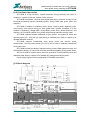
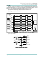
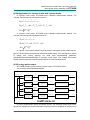
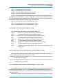
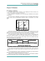
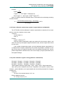
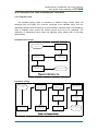
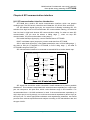
SPI reading timing:
CS
SCLK
DIN
76543210
DOUT
23 22 21 20 19 18 17 16 15 14 13 12 11 10 9 8 7 6 5 4 3 2 1 0
Diagram 4-2-1 SPI reading timing
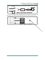
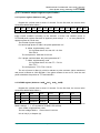
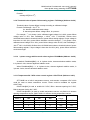
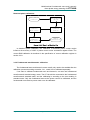
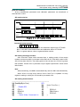
Command format meaning:
7
6
5
4
3
2
1
0
Bit7=0: host MCU read measurement and calibration register from ATT7022B.
Bit7=1: host MCU write measurement and calibration data to ATT7022B.
Bit6...0: register address, refer to register definition section.
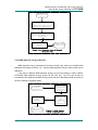
SPI reading working procedure:
After host MCU writes 8-bits command byte, a waiting period of time maybe
needed, and then host MCU could read 24-bits data via SPI. Host MCU needn’t wait if
SCLK is less than 200 KHz. The waiting period of time is about 3us if SCLK is greater
than 200KHz. Please refer to parameter output register specification section about
data formats.
Note:
When transferring, the MSB is transmitted firstly and the LSB is transmitted lastly.
When SCLK is at high level, data on DIN or DOUT pin is updated. At every
register’s reading or writing the CS should be processed once.
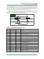
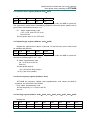
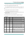
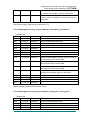
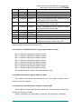
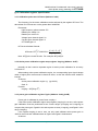
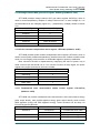
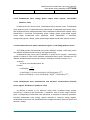
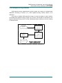
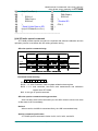
SPI reading demonstration:
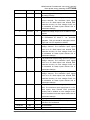
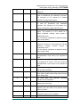
--------------------------------------------------------------------01| ReadSpi(Byte Com)
SPI
02| {
08|
for(n=7;n>=0;n--)
03|
; Enable SPI
09|
{
04|
CS=1;
10|
SCLK=1;
05|
SCLK=0;
11|
DIN=Com.n;
06|
CS=0;
12|
SCLK=0;
07|
; Send 8-bits Command to
13|
}
http://www.Actions.com.cn
Page 49 of 54
Rev 1.04