1
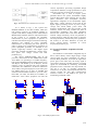
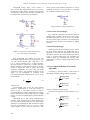
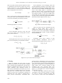
Sensors & Transducers, Vol. 180, Issue 10, October 2014, pp. 174-180 Sensors & Transducers © 2014 by IFSA Publishing, S. L. http://www.sensorsportal.com The System Developing of Intelligent and High-precision Power Parameter Measurement in Power System Based on Power Spectral Density Algorithm Huimin ZHANG Department of Communication, Chongqing College of Electronic Engineering, Chongqing 401331, China Tel.: +8613206006614 E-mail: [email protected] Received: 28 July 2014 /Accepted: 30 September 2014 /Published: 31 October 2014 Abstract: In modern power systems, high-precision power parameter measurement has occupied an important position for power quality in power grids. This paper presents a high-precision intelligent power parameter measurement device, which can collect parallel alternative current parameter values among 0 to 250 V in 3-channel easily and quickly, and improve the measurement accuracy by using the power spectral correction algorithm for sample parameters. The ATT7022B chip is used as the front-end of the data acquisition, and we use STM32 chip as the processor, which is easy to implement the algorithm on this platform. Results obtained from test application of the entire system show that the system has advantages of stable performance, small size, high reliability, and excellent accuracy. Copyright © 2014 IFSA Publishing, S. L. Keywords: Power parameters, Power spectral density, High-precision, Measurement, ATT7022B. 1. Introduction Electrical energy has become a part of our life; therefore, and power quality is related to all aspects of our social life. The measurements of these parameters are directly reflected in the power quality of the power supply, therefore monitoring power parameters in power grids has important practical significance [2]. Due to the wide coverage of power grids, there is a considerable number of disperse nodes need to detect. Therefore that how to monitor the power parameters in real-time effectively is still required to be continually studied. According to this situation, we designed a high-precision intelligent power parameter measurement device which can quickly and easily achieve a single system of parallel acquiring parameter values from 0 to 250 V in 3-channel; the power parameter measurement in this paper mainly discusses the measurements of voltage 174 RMS (URMS), the current RMS (IRMS), the apparent power (S), the active power (P), the power factor (σ) and other parameters of alternative current working at 50 Hz, then correct the sampled parameters by using power spectral algorithm to improve the electric parameter measurement accuracy. The results show that the system has advantages of stable performance, small size, high reliability, and excellent accuracy. 2. Hardware Design 2.1. System Design According to the demand for measuring power parameter, we build a wireless network monitoring system. The structure is shown in Fig. 1. http://www.sensorsportal.com/HTML/DIGEST/P_2456.htm Sensors & Transducers, Vol. 180, Issue 10, October 2014, pp. 174-180 Fig. 1. Measurement error characteristics of sensor. As is shown in Fig. 1, the system uses STM32F103RET6 as the main module, which has rich on-chip resources of peripheral module, to expand trunk RS232 (UART), Power Measurement Module (SPI) and other functions. The main function of the system is to complete the parameter measurement of power equipment in operation in real-time and reach the target of real time monitoring. Therefore, the module of power parameter measurement is an important part of the system. In order to getting more comprehensive parameters of power equipment operation, we decided to use specific single-chip solution, with digital signal processing methods simultaneously capture threewire power line voltage, current and other parameters [5]. We choose STM32F103RET chip as the processor, which based on the ARM®Cortex™-M3 32-bit RISC core operating at a 72 MHz frequency, high-speed embedded memories (Flash memory up to 512 Kbytes and SRAM up to 64 Kbytes), and an extensive range of enhanced I/Os and peripherals connected to two APB buses. All devices offer three 12-bit ADCs, four general-purpose 16-bit timers plus two PWM timers [8], as well as standard and advanced communication interfaces: up to two I2Cs, three SPIs, two I2Ss, one SDIO, five USARTs, an USB and a CAN. These properties can meet the AT7022-CF1 VOUT-OUT AT7022-CF3 control, acquisition, processing algorithms design requirements. Besides, its high performance to price ratio also is the one of reasons why we choose it. ATT7022B chip is used to acquire power parameter data in our system. ATT7022B is highly accurate three-phase power metering chip, for threephase three-wire and three-phase four-wire applications; integration of six second-order sigmadelta ADC, voltage reference circuit and all the digital signal processing circuits of power, energy, voltage and current RMS, power factor and frequency measurement. This chip provides an SPI interface, which can easily transmit the data of measurement parameters and table parameters between the external MCU and itself. Besides, its internal voltage monitoring circuit can guarantee it working properly when the chip power on and off. The chip can directly measure the power parameters, but accuracy is not ideal. Therefore, we must use power spectral density algorithm to correct acquisition parameters [9]. 2.2. Power Parameter Acquisition Circuit Design ATT7022B is a semiconductor integrated chip so that it cannot directly connect high voltage or high current signal for power parameters. In order to measure these parameters, we isolate the signal from power grid, at the same time, the strong signal is converted to small one, and then put these converted signal into ATT7022B for measuring. ATT7022B peripheral circuit is referred to the chip manual, we can see it in Fig. 2. Avoiding unnecessary interference, we let part of unused pins disconnect or connect ground; the chip SPI communication interface connect to the STM32 I/O ports for transmitting command or data. DGND VOUT-OUT DGND 24.576MHZ R11 330R DGND P1 U4 P521 VOUT-OUT 6 5 4 3 2 1 OUT-CF1 OUT-CF2 OUT-CF3 OUT-CF4 R12 10K OUT-CF2 GND-OUT AT7022-CF4 R13 330R DGND VDD5V0 VDD3V3 GND-OUT VOUT-OUT U5 P521 C2 15P DGND R14 10K OUT-CF4 AT7022-REST AT7022-SIG V1P V1N GND-OUT C9 10uF/16V AGND V3P C10 V3N 104 V5P V5N REFO C11 104 Header 6GND-OUT AGND 1 2 3 4 5 6 7 8 9 10 11 A T 7022-D O U A T 7022-D IN A T 7022-S CK A T 7022-CS P521 C1 Z1 15P R6 10K OUT-CF3 A T 7022-RE V P VOUT-OUT DGND U2 VDD5V0 44 43 42 41 40 39 38 37 36 35 34 AT7022-CF2 GND-OUT R5 330R VDD NC CF4 CF3 NC CF2 CF1 SEL NC TEST GND GND O S CO O S CI V CC RE V P VDD DOUT D IN S CL K CS V CC P521 DGND R4 10K OUT-CF1 REST SIG V1P V1N REFCAP V3P V3N AGND V5P V5N REFOUT A V CC V 2P V 2N AGND V 4P V 4N A V CC V 6P V 6N V 7P V 7N U1 12 V 2P 13 V 2N 14 15 V 4P 16 V 4N 17 18 V 6P 19 V 6N 20 V 7P 21 V 7N 22 R3 330R VDD5V0 U3 33 32 31 30 29 28 27 26 25 24 23 VDD3V3 AT7022-CF4 AT7022-CF3 AT7022-CF2 AT7022-CF1 AT7022-SEL DGND DGND ATT7022D VDD5V0 Fig. 2. ATT7022B peripheral circuit. 175 Sensors & Transducers, Vol. 180, Issue 10, October 2014, pp. 174-180 ATT7022B analog input circuit shown in Fig. 3. Firstly, the voltage directly access into circuit, through the voltage divider, and then superimposed on a reference voltage signal. Finally, this signal will be transmit into A/D converter for sampling. resistor and IC input parasitic capacitance C can be combined to become a low-pass filter to eliminate any oscillation of SPI interface signals. Fig. 4. Reference voltage input interface. (a) 2.3. Processor Circuit Design Fig. 5 illustrates the mini-system circuit design of STM32, which includes a reset circuit, clock circuit, and STM32 processor circuit. As we can see, STM32 not only controls logic controller to send the data, but also communicate with the PC via RS232 or RS485 interface. 2.4. PCB Layout Design (b) Fig. 3. (a) The measured voltage input interface; (b) current detection input interface. From ATT7022B chip manual, we know that ATT7022B voltage channel input range from 0 V to 1 V, the current channel input range from 2 mV to 1 V. And its sampling rate is 3.2 kHz, therefore, the input frequency greater than 1.6 kHz will form aliasing frequency at low frequency band; we usually choose a simple RC filter to filter these high frequency components. For power chip, the useful signal only near by the sampling frequency of the signal, so the bandwidth is generally from 0 to 2 KHz. The filter cutoff frequency is fL=1.3k, by the formula are: 1 , fL = 2π RC 3. Power Spectral Density Correction Algorithm According to electrical theory, valid values of periodically changing voltage and current signals: U= 1 T 2 u (t )dt , T 0 (2) I= 1 T 2 i (t )dt , T 0 (3) (1) where R=12k. In ATT7022B, each of the AC input channel requires a superposition of a DC bias voltage, as shown in Fig. 4. The REFO resistor is used to provide the DC bias voltage, and the DC bias voltage can be obtained by the chip voltage reference voltage output, or can be provided from an external reference voltage. ATT7022B has a SPI serial communication interface, which communicates in slave mode having two control lines and two data lines: CS, SCLK, DIN, and DOUT. Considering the SPI transmission signal line may be disturbed or jitter, so we put a small resistor (10Ω) in series with the signal line. This 176 We design two-layers PCB board for our system by using Altium Designer, the PCB board size is supposed to meet the size requirements of external mechanical structure, the system board layout shown in Fig. 6. System board layout, the minimum line width of 8mil, the minimum line spacing 8mil, smallest hole is 16mil, is a high wiring density on the PCB board. where T is the period of the signals. We discretize Equation (2) and Equation (3), we have U= I= N −1 1 N u 1 N i 2 ( n) , (4) (n) , (5) n =0 N −1 n =0 2 Sensors & Transducers, Vol. 180, Issue 10, October 2014, pp. 174-180 U6 AT7022-REST PA0/U2_CTS CR1 0 AT7022-CS AT7022-SCK AT7022-DOU AT7022-DIN 14 15 16 17 20 21 22 23 PA2/U2_TX PA3/U2_RX CR2 CR3 CR4 CR5 0 0 0 0 0 CR6 PA9/U1_TX PA10/U1_RX CR7 AT7022-SEL 0 AT7022-REVP 0 PA13/TMS CR8 PA14/TCK PA15/TDI C18 DSGND C20 1 22P 2 AT7022-SIG 41 42 43 44 45 46 49 50 NRESET 22P PC0 PC1 PC2 PC3 PC4 PC5 PC6 PC7 BOOT0 7 NRST R29 10K DSGND PB8 PB9 PB10 PB11 PB12 PB13 PB14 PB15 OSC_IN/PD0 OSC_OUT/PD1 PD2 60 R36 10K 1 VDD3V3 C24 104 VBAT 32 48 64 19 DSGND VDD3V3 L3 13 10mH C28 C29 0.1U 10U VDD_1 VDD_2 VDD_3 VDD_4 VSS_1 VSS_2 VSS_3 VSS_4 VDDA VSSA PB0 PB1 PB2 PB3/TDO PB4/TRST PB5 PB6/I2C1_SCL PB7/I2C1_SDA 61 62 29 30 33 34 35 36 PB8 PB9 PB10/U3_TX PB11/U3_RX PB12/U3_CK PB13/U3_CTS PB14/U3_RTS PB15 8 9 10 11 24 25 37 38 PC0 PC1 PC2 PC3 PC4 PC5 LED1 LED2 39 40 51 52 53 2 3 4 PC8 PC9 PC10 PC11 PC12 PC13-TAMPER-RTC PC14-OSC32_IN PC15-OSC32_OUT VDD3V3 NRESET 26 27 28 55 56 57 58 59 PB0 PB1 PB2/BOOT1 PB3/JTDO PB4/JNTRST PB5 PB6 PB7 PA8 PA9 PA10 PA11 PA12 PA13/JTMS/SWDIO PA14/JTCK/SWCLK PA15/JTDI 5 6 54 PD2 Y1 8MHz PA0-WKUP PA1 PA2 PA3 PA4 PA5 PA6 PA7 R24 10K DSGND LED3 PC9/SDIO_D1 PC10/SDIO_D2/USART4_TX PC11/SDIO_D3/USART4_RX PC12/SDIO_CK/USART5_TX PC13 PC14 PC15 32.768K 2 1 31 47 63 18 C25Y2 6.8P 12 C26 6.8P DSGND STM32F103R6T6 DSGND VDD3V3 DSGND C33 C35 0.1U 0.1U C36 0.1U C37 0.1U DSGND 1 2 2 23 24 25 7 26 28 27 6 29 30 31 32 33 2 2 21 15 14 13 1 2 1 12 21 2 1 2 7 1 2 9 11 8 5 4 3 2 1 2 2 21 1 1 2 1 2 1 1 2 1 1 2 2 2 2 1 1 1 1 2 2 1 2 1 4 1 2 2 1 1 2 2 1 1 1 2 2 2 0 1 1 1 2 1 2 2 1 1 2 1 1 2 1 4 1 2 1 2 2 2 1 1 1 2 1 4 5 2 3 3 2 2 2 2 2 3 6 2 2 7 1 4 1 1 1 8 3 3 1 2 2 2 3 2 1 1 2 5 1 2 2 1 1 2 6 1 1 2 1 4 4 8 9 2 2 4 2 1 2 1 7 10 2 6 11 1 1 4 2 5 12 2 2 2 2 1 5 1 5 4 13 1 2 1 3 2 3 14 2 1 2 1 2 15 4 12 2 1 1 1 16 2 2 6 6 1 2 3 3 3 1 2 1 1 2 1 2 2 1 2 1 1 7 10 2 1 1 1 2 1 12 1 2 1 1 2 2 44 1 2 2 2 2 43 2 1 2 42 2 1 1 2 1 1 2 1 1 1 2 41 2 1 8 8 1 2 2 16 2 1 40 2 1 1 17 18 2 39 38 1 37 19 36 20 2 2 1 1 2 2 19 17 15 13 11 9 7 5 1 1 2 35 21 12 1 9 22 2 9 34 2 1 1 20 18 16 14 12 8 10 4 3 6 2 1 1 10 10 2 1 1 3 4 1 Fig. 5. Mini-system circuit design of STM32. Fig. 6. System board layout. 177 Sensors & Transducers, Vol. 180, Issue 10, October 2014, pp. 174-180 where u(n) and i(n) are the discrete sequences, which is transformed from measured voltage and current signals respectively by the sampling, holding and A/D conversion. N is a frequency period of sampling points. Single-phase active power is: P = UI cos φ , (6) where U and I are the voltage and current RMS, cosϕ is the power factor of the load. Besides, active power can also be calculated by the following formula: P= 1 T T 0 u (t )i (t ) dt , (7) Fig. 7. RMS measurement block diagram. Discretizing Equation (7), we have P= 1 N N −1 u (n)i(n) , (8) n=0 In the three-phase four-wire circuit, the total active power equal to sum of each phase of active power, can be written as: P = PA + PB + PC , (9) In three-phase three-wire circuit, the total active power can be measured by two-Wattmeter method: P = PAC + PBC , Power parameters of the sampling system can provide fundamental, harmonics and voltage of each phase and three-phase full-wave RMS voltage vector, and a full-wave current RMS, and RMS phase current vector. Grid voltage signal is converted to the sampling values by ADC of ATT7022B chip; and then, it can be sent to the STM32 processor family unit operation; finally, we can get its RMS value. After reading the corresponding value of the register, we right 13 bit to obtain the required measurements. Measurement block diagram shown in Fig. 7: When we remove the DC component from the voltage or current signals, after a series of multiplications, additions, and digital filtering; we can get the active power of each phase. Voltage and current sampling data contains 21-order harmonic, and based formula is: P = 1 N N U (n ) I (n ) , (11) n=0 Calculating active power contains at least 21-order harmonic information. Active power measurement block diagram shown in Fig. 8, is (10) Pt =Pa +Pb +Pc . Fig. 8. Active power measurement block diagram. 4. Testing When we calibrate the power meter of power parameter measurement, we must provide a standard meter. Compared with standard meter, only the active should be calibrated and reactive power does not require calibration. After calibrated, accuracy of active power measurement can achieve up to 0.5s. Power correction is divided into ratio error correction and phase error correction. Ratio error correction removes the ratio error in transformer. Nonlinear of transformer ratio error cannot be ignored when it needs precision measurement. ATT7022B offers 178 register Iregchg, compensation can be set based on the current size of the staging area. Besides, phase error correction also can be corrected segmentally. In applications, the segments do not need to separate too small. Phase error correction should do after completing ratio error correction. Ratio error correction should be performed when power factor equal to 1.0, and phase error correction should be performed at 0.5 L [10]. We can read register HFConst directly from ATT7022B to know the pulse frequency of output CF, which is selected to calibrate the meter. HF Const cannot be written more than 0x000D00 of Sensors & Transducers, Vol. 180, Issue 10, October 2014, pp. 174-180 parameter values. The constant frequency pulse is EC, rated input voltage is Un, rated input current is Ib, voltage of sampling voltage channel is Vu, voltage of sampling current channel is Vi, ATT7022B gain is G. Therefore, we calculate the value of HF Const: G 2 ×Vu ×VI , HFConst =INT 5760000000 × U n × Ib × EC (12) where INT[] means to take the integer part. When Ugain=0, voltage correction register can be read directly from ATT7022B by SPI interface, the value is DataU. Then, we can read the actual input voltage RMS Ur from standard meter. We know actual input voltage RMS is Ur, measuring voltage RMS is U rms = DataU × 210 223 , so we have U gain =U r U rms -1 , (13) If U gain ≥ 0 , U gain = INT U gain × 223 , U gain <0 , U gain = INT 224 +U gain × 223 . The RMS output register of ATT7022B is supplementary code, the highest bit is the sign bit; RMS is always greater than or equal to 0, so the maximum sign bit is always equal to 0. The 24-bit data Vrms convert to actual voltage RMS is U rms =Vrms × 210 2 23 , (14) The reference power spectral density correction algorithm to correct for acquisition parameters, the main process of calibration: Parameter settings, A phase correction, B phase correction, C phase correction. Where the parameter set is divided into: the voltage channel ADC gain select, high-frequency pulse output setting, ratio error compensated area setting, phase compensation area setting, loss of pressure threshold setting, the starting current setting, energy accumulation mode setting, and the other parameters of the phase correction steps: Power gain correction (Pf=1.0), phase error correction (Pf=0.5 L), voltage correction (rated voltage), current correction (rated current). Test environment: Laboratory temperature Test objects: 220 V/25 W incandescent, 220 V/60 W incandescent, transformers power supply. As we can see from the Table 1, the power parameters, which correct by power spectral density power correction algorithm, differ from the nominal value. But the result is same with the test values of standard correction meter, indicating that the system is able to achieve high-precision measurement of power parameters [11]. Table 1. Test Results. Test object Voltage RMS Current RMS Power 220 V/25 W incandescent 213.3 V 0.12 A 25 W 220 V/60 W incandescent 212.5 V 0.27 A 57 W 9 W transformers power supply 217.6 V 0.04 A 9W 5. Conclusion This paper presents a developing method of high-precision power parameter measurement equipment based on power spectral density correction. This method can correct power parameter error, and has high precision in correction. Besides, the algorithm is simple and is very suitable for highprecision measurement of power parameters. However, because the power parameter measurement device itself can only collect three voltage and current values, the accuracy of the data must be referred to standard measuring instruments and it cannot achieve self-correcting, which leads to the range of application of high-precision power parameter measurement devices in some extent will be restricted. Acknowledgements Chongqing Vocational and Technical College Applied Technology Promotion Center Projects to promote the application of new technologies "STM32-based wireless lights integrated management system". Reference [1]. SUN He-lin, Lu Yuan-long, TIAN Yue-jun, Remote power quality monitoring system based on GPRS and virtual instruments, Relay, Vol. 35, Issue 1, 2007, pp. 59-62. [2]. Sun Guo-dong, Lei Zai-shuan, Zhou Yu-guo, et al., Design of Comprehensive Electrical Power Monitoring Device, Electrical Measureme Instrumentation, Vol. 44, Issue 7, 2007, pp. 37-40. [3]. Lei,Yang, Guang-ming, Huang, et al., The realization of automatic correction table platform, Electrical Measurement & Instrumentation, Vol. 44, Issue 5, 2007, pp. 58-60. [4]. Chen Tao, He Wei, Liu Xiao-Ming, et al., An on-line ultraviolet detecting system of EHV transmission lines, Automation of Electric Power Systems, Vol. 29, Issue 7, 2005, pp. 88-92. [5]. Liu Hai-Chang, Liu Hao, Wang Jiao-Xia, et al., Design and implementing of remote power quality monitoring system, Power System Protection and Control, Vol. 37, Issue 1, 2009, pp. 109-111. 179 Sensors & Transducers, Vol. 180, Issue 10, October 2014, pp. 174-180 [6]. Intel Corporation. Intel MCS-51 microcontroller family user’s manual. http://www.intel.com, 2006-05-20. [7]. Li Xia, Sun Hui, A novel divider based on dual-bit algorithm, Chinese Journal of Semiconductors, Vol. 25, Issue 6, 2004, pp. 645- 649. [8]. Wei J. D., Sun C. T., Constructing hysteresis memory in neural networks, IEEE Transactions Systems Man Cybernetics, Vol. 30 Issue 4, 2000, pp. 601-609. [9]. Jang X. G., A CCD driver based on programmable logic device, J. Foreign Electronic Elements, Vol. 11, 1996, pp. 41-43. [10]. Ai L. L., Yuan F., Ding ZH. L., Measurement of spatial object. s exterior attitude based on linear CCD, Chinese Optics Letters, 2008, Vol. 6, Issue 7, pp. 505-509. [11]. Texas Instrument, CC2430 Datasheet, 200715. ___________________ 2014 Copyright ©, International Frequency Sensor Association (IFSA) Publishing, S. L. All rights reserved. (http://www.sensorsportal.com) 180