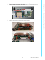
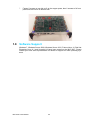
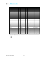
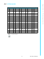
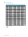
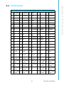
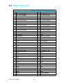
1
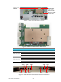
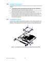
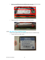
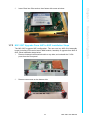
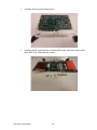
User Manual MIC-3397 6U CompactPCI® 3rd Generation Intel® Quad-Core Xeon® & Dual-Core Pentium® Processor Blade with ECC support Copyright The documentation and the software included with this product are copyrighted 2014 by Advantech Co., Ltd. All rights are reserved. Advantech Co., Ltd. reserves the right to make improvements in the products described in this manual at any time without notice. No part of this manual may be reproduced, copied, translated or transmitted in any form or by any means without the prior written permission of Advantech Co., Ltd. Information provided in this manual is intended to be accurate and reliable. However, Advantech Co., Ltd. assumes no responsibility for its use, nor for any infringements of the rights of third parties, which may result from its use. Acknowledgements Intel®, Pentium® & Xeon® are trademarks of Intel Corporation. Microsoft® Windows® and MS-DOS® are registered trademarks of Microsoft Corp. All product names or trademarks are properties of their respective owners. Product Warranty (2 years) Advantech warrants to you, the original purchaser, that each of its products will be free from defects in materials and workmanship for two years from the date of purchase. This warranty does not apply to any products which have been repaired or altered by persons other than repair personnel authorized by Advantech, or which have been subject to misuse, abuse, accident or improper installation. Advantech assumes no liability under the terms of this warranty as a consequence of such events. Because of Advantech’s high quality-control standards and rigorous testing, most of our customers never need to use our repair service. If an Advantech product is defective, it will be repaired or replaced at no charge during the warranty period. For outof-warranty repairs, you will be billed according to the cost of replacement materials, service time and freight. Please consult your dealer for more details. If you think you have a defective product, follow these steps: 1. Collect all the information about the problem encountered. (For example, CPU speed, Advantech products used, other hardware and software used, etc.) Note anything abnormal and list any onscreen messages you get when the problem occurs. 2. Call your dealer and describe the problem. Please have your manual, product, and any helpful information readily available. 3. If your product is diagnosed as defective, obtain an RMA (return merchandize authorization) number from your dealer. This allows us to process your return more quickly. 4. Carefully pack the defective product, a fully-completed Repair and Replacement Order Card and a photocopy proof of purchase date (such as your sales receipt) in a shippable container. A product returned without proof of the purchase date is not eligible for warranty service. 5. Write the RMA number visibly on the outside of the package and ship it prepaid to your dealer. MIC-3397 User Manual Part No. 200K339700 Edition 1 Printed in China December 2014 ii Declaration of Conformity CE This product has passed the CE test for environmental specifications when shielded cables are used for external wiring. We recommend the use of shielded cables. FCC Class A Note: This equipment has been tested and found to comply with the limits for a Class A digital device, pursuant to part 15 of the FCC Rules. These limits are designed to provide reasonable protection against harmful interference when the equipment is operated in a commercial environment. This equipment generates, uses, and can radiate radio frequency energy and, if not installed and used in accordance with the instruction manual, may cause harmful interference to radio communications. Operation of this equipment in a residential area is likely to cause harmful interference in which case the user will be required to correct the interference at his own expense. FM This equipment has passed the FM certification. According to the National Fire Protection Association, work sites are classified into different classes, divisions and groups, based on hazard considerations. This equipment is compliant with the specifications of Class I, Division 2, Groups A, B, C and D indoor hazards. Technical Support and Assistance 1. 2. Visit the Advantech website at http://support.advantech.com where you can find the latest information about the product. Contact your distributor, sales representative, or Advantech's customer service center for technical support if you need additional assistance. Please have the following information ready before you call: – Product name and serial number – Description of your peripheral attachments – Description of your software (operating system, version, application software, etc.) – A complete description of the problem – The exact wording of any error messages iii MIC-3397 User Manual Warnings, Cautions and Notes Warning! Warnings indicate conditions, which if not observed, can cause personal injury! Caution! Cautions are included to help you avoid damaging hardware or losing data. e.g. There is a danger of a new battery exploding if it is incorrectly installed. Do not attempt to recharge, force open, or heat the battery. Replace the battery only with the same or equivalent type recommended by the manufacturer. Discard used batteries according to the manufacturer's instructions. Note! Notes provide optional additional information. Document Feedback To assist us in making improvements to this manual, we would welcome comments and constructive criticism. Please send all such - in writing to: [email protected] Packing List Before setting up the system, check that the items listed below are included and in good condition. If any item does not accord with the table, please contact your dealer immediately. MIC-3397 all-in-one single board computer (CPU heatsink, PCH heatsink & MXM heatsink, and E6760 MXM Type A module optional included) x1 Daughter board for SATA HDD & SATA bracket (assembled) x 1 Solder-side cover (assembled) x1 HDD screws x 4, CFast screw x 1, RJ45 to DB9 cable x1 (accessories) Warranty certificate document x1 Safety Warnings: CE, FCC class A MIC-3397 User Manual iv Safety Instructions 1. 2. 3. Read these safety instructions carefully. Keep this User Manual for later reference. Disconnect this equipment from any AC outlet before cleaning. Use a damp cloth. Do not use liquid or spray detergents for cleaning. 4. For plug-in equipment, the power outlet socket must be located near the equipment and must be easily accessible. 5. Keep this equipment away from humidity. 6. Put this equipment on a reliable surface during installation. Dropping it or letting it fall may cause damage. 7. The openings on the enclosure are for air convection. Protect the equipment from overheating. DO NOT COVER THE OPENINGS. 8. Make sure the voltage of the power source is correct before connecting the equipment to the power outlet. 9. Position the power cord so that people cannot step on it. Do not place anything over the power cord. 10. All cautions and warnings on the equipment should be noted. 11. If the equipment is not used for a long time, disconnect it from the power source to avoid damage by transient overvoltage. 12. Never pour any liquid into an opening. This may cause fire or electrical shock. 13. Never open the equipment. For safety reasons, the equipment should be opened only by qualified service personnel. 14. If one of the following situations arises, get the equipment checked by service personnel: The power cord or plug is damaged. Liquid has penetrated into the equipment. The equipment has been exposed to moisture. The equipment does not work well, or you cannot get it to work according to the user's manual. The equipment has been dropped and damaged. The equipment has obvious signs of breakage. 15. DO NOT LEAVE THIS EQUIPMENT IN AN ENVIRONMENT WHERE THE STORAGE TEMPERATURE MAY GO BELOW -20° C (-4° F) OR ABOVE 60° C (140° F). THIS COULD DAMAGE THE EQUIPMENT. THE EQUIPMENT SHOULD BE IN A CONTROLLED ENVIRONMENT. 16. CAUTION: DANGER OF EXPLOSION IF BATTERY IS INCORRECTLY REPLACED. REPLACE ONLY WITH THE SAME OR EQUIVALENT TYPE RECOMMENDED BY THE MANUFACTURER, DISCARD USED BATTERIES ACCORDING TO THE MANUFACTURER'S INSTRUCTIONS. The sound pressure level at the operator's position according to IEC 704-1:1982 is no more than 70 dB (A). DISCLAIMER: This set of instructions is given according to IEC 704-1. Advantech disclaims all responsibility for the accuracy of any statements contained herein. v MIC-3397 User Manual Safety Precaution - Static Electricity Follow these simple precautions to protect yourself from harm and the products from damage. To avoid electrical shock, always disconnect the power from your PC chassis before you work on it. Don't touch any components on the CPU card or other cards while the PC is on. ESD (electrostatic discharge) can cause either catastrophic or latent damage in sensitive electronic components. Take appropriate measures to ensure that any accumulated body charge is removed before accessing electronic devices. A static-safe workbench is ideal. We Appreciate Your Input Please let us know of any aspect of this product, including the manual, which could use improvement or correction. We appreciate your valuable input in helping make our products better. MIC-3397 User Manual vi Contents Chapter 1 Hardware Configuration......................1 1.1 Introduction ............................................................................................... 2 Table 1.1: MIC-3397 Variants...................................................... 3 Specifications ............................................................................................ 3 1.2.1 CompactPCI Bus Interface ........................................................... 3 1.2.2 CPU .............................................................................................. 3 Table 1.2: CPU Variants.............................................................. 3 1.2.3 BIOS ............................................................................................. 3 1.2.4 Chipset.......................................................................................... 4 Table 1.3: MIC-3397 with 8HP-1 I/O Features ............................ 4 Table 1.4: MIC-3397 with 8HP-2 I/O Features ............................ 4 1.2.5 Memory ......................................................................................... 4 1.2.6 Ethernet ........................................................................................ 4 1.2.7 Storage Interface .......................................................................... 5 Table 1.5: Storage ....................................................................... 5 1.2.8 Serial Interface.............................................................................. 5 1.2.9 USB Port ....................................................................................... 5 1.2.10 LEDs ............................................................................................. 5 Table 1.6: LED Indicator for the MIC-3397.................................. 5 1.2.11 Watchdog Timer............................................................................ 5 1.2.12 Optional Rear I/O Modules ........................................................... 6 Table 1.7: RIO Configurations ..................................................... 6 1.2.13 Optional Extension Modules ......................................................... 6 Table 1.8: The Second Layer XTM (8HP) Configurations ........... 6 1.2.14 Mechanical and Environmental Specifications.............................. 6 1.2.15 Compact Mechanical Design ........................................................ 7 1.2.16 CompactPCI Bridge ...................................................................... 7 1.2.17 Hardware Monitor ......................................................................... 7 1.2.18 Super I/O....................................................................................... 7 1.2.19 RTC and Battery ........................................................................... 8 1.2.20 Drone Mode .................................................................................. 8 Functional Block Diagram ......................................................................... 8 Figure 1.1 MIC-3397 functional block diagram. ........................... 8 Jumpers and Switches .............................................................................. 8 Table 1.9: MIC-3397 jumper descriptions.................................... 9 Figure 1.2 MIC-3397 jumper locations......................................... 9 Table 1.10: MIC-3397 8HP Jumper Descriptions .......................... 9 Figure 1.3 MIC-3397 COM3 switch setting................................ 10 Figure 1.4 MIC-3397 COM4 switch setting................................ 10 Figure 1.5 MIC-3397 8HP Display Port switch setting............... 11 Figure 1.6 MIC-3397 switch locations........................................ 11 Connector Definitions.............................................................................. 12 Table 1.11: MIC-3397 4HP Connector Descriptions ................... 12 Table 1.12: MIC-3397 8HP Connector Descriptions ................... 12 Figure 1.7 MIC-3397 8HP-1 Front Panel Ports, Indicators, Buttons.... 13 Figure 1.8 MIC-3397 8HP-2 Front Panel Ports, Indicators, Buttons.... 13 Figure 1.9 MIC-3397 8HP-1 side view....................................... 13 Figure 1.10MIC-3397 8HP-2 side view....................................... 14 Figure 1.11RIO Panel Ports........................................................ 14 Figure 1.12RIO 4HP side view ................................................... 14 Figure 1.13RIO 8HP side view ....................................................15 Table 1.13: MIC-3397 4HP Rear I/O Connector Descriptions..... 15 Table 1.14: MIC-3397 8HP Rear I/O Connector Descriptions..... 15 Safety Precautions .................................................................................. 16 1.2 1.3 1.4 1.5 1.6 vii MIC-3397 User Manual 1.7 Chapter 1.8 1.9 Installation Steps..................................................................................... 17 1.7.1 MIC-3397 Installation Steps........................................................ 17 Figure 1.14MIC-3397 8HP-1 assembly ...................................... 17 Figure 1.15MIC-3397 8HP-2 assembly ..................................... 17 1.7.2 MIC-3397 Rear I/O Board Installation Steps .............................. 18 Figure 1.16MIC-3526 RIO for MIC-3397 8HP assembly ............ 18 1.7.3 MIC-3397 Board Installation in PlusIO System........................... 18 Figure 1.17MIC-3397 Application in PlusIO system ................... 18 Battery Replacement .............................................................................. 19 Software Support .................................................................................... 19 2 AMI BIOS Setup................................. 21 2.1 Introduction ............................................................................................. 22 Figure 2.1 Setup program initial screen..................................... 22 Entering Setup ........................................................................................ 23 Figure 2.2 Press <DEL> or <F2> to run setup .......................... 23 2.2.1 Main Setup.................................................................................. 24 Figure 2.3 Main setup screen .................................................... 24 2.2.2 Advanced BIOS Features Setup................................................. 25 Figure 2.4 Advanced BIOS features setup screen .................... 25 Figure 2.5 Trusted Computing................................................... 26 Figure 2.6 CPU configuration .................................................... 27 Figure 2.7 SATA configuration .................................................. 28 Figure 2.8 USB configuration .................................................... 29 Figure 2.9 H/W Monitor configuration........................................ 30 Figure 2.10Super IO configuration ............................................. 31 Figure 2.11Serial Port Console Redirection configuration.......... 32 Figure 2.12Network Stack configuration..................................... 33 Figure 2.13CPU PPM configuration ........................................... 34 2.2.3 Chipset Setup ............................................................................. 35 Figure 2.14Chipset setup ........................................................... 35 Figure 2.15PCH-IO Configuration .............................................. 35 Figure 2.16PCI Express configuration........................................ 36 Figure 2.17USB configuration .................................................... 36 Figure 2.18System Agent configuration ..................................... 37 Figure 2.19Graphics configuration ............................................. 38 Figure 2.20NB PCIe configuration.............................................. 38 2.2.4 Boot Setup .................................................................................. 39 Figure 2.21Boot setup ................................................................ 39 Figure 2.22CSM16 Parameters setting ...................................... 40 2.2.5 Security Setup ............................................................................ 41 Figure 2.23Password configuration ............................................ 41 2.2.6 Save & Exit Option...................................................................... 42 Figure 2.24Save and Exit configuration...................................... 42 2.2 Appendix A Pin Assignments............................... 45 A.1 J1 Connector........................................................................................... 46 Table A.1: J1 CompactPCI I/O .................................................. 46 J2 Connector........................................................................................... 47 Table A.2: J2 CompactPCI I/O .................................................. 47 Other Connectors.................................................................................... 48 Table A.3: XTM Board Connector (CN1, CN4, CN8, CN9) ....... 48 Table A.4: XMC Connector........................................................ 50 Figure A.1 RJ45 LAN Indicator .................................................. 50 A.2 A.3 MIC-3397 User Manual viii Appendix B CPLD ...................................................51 B.1 B.2 B.3 Features .................................................................................................. 52 CPLD Introduction................................................................................... 52 Watchdog Timer...................................................................................... 52 Appendix C Glossary .............................................53 C.1 Glossary .................................................................................................. 54 ix MIC-3397 User Manual MIC-3397 User Manual x Chapter 1 1 Hardware Configuration This chapter describes how to configure MIC-3397 hardware. 1.1 Introduction Advantech’s MIC-3397 series is a 6U CompactPCI single board computer with Intel® Quad-Core Xeon® E3-1125C v2 (40W)/E3-1105C v2 (25 W) server class processor, and Intel® Dual-Core Pentium® B925C (15 W) low power dissipation processor, with DH8900 chipset that supports DMI1.0 x 4 FSB. The processor uses Intel® 22nm 64 bit process technology, with up to 2.5 GHz clock speed, 8 MB L3 cache featuring Intel® Hyper-Threading, Virtualization, Trusted Execution Technology, which enables the board to meet the highest standards for the management and security of highavailability applications. It supports dual-channel ECC memory, up to 16 GB DDR3 of 1333/1600 MHz with max 8 G on board and 8 G SO-DIMM memory, three 2.5” Serial ATA interfaces (one on board optional with one 8 GB NAND flash, two to RTM), one Cfast slot, five Gigabit Ethernet ports (two on front panel, two to PCIMG2.16, two to RTM with one optional on front panel), six USB2.0 ports (three on front panel, three to RTM), two VGA ports (one on front panel, one to RTM) on 4HP, three COM ports (one to front panel, two to RTM), one PS/2 port, and one PCIe2.0 x4 interface reserved for user defined rear transition module. MIC-3397, is designed in single slot (4HP) and dual slot (8HP) form factor widths. The 8HP version provides rich and extensive I/O support, features high-performance discrete graphics using AMD Radeon E6760 GPU, supports 1 GB GDDR5 at PCIe x1, x2, x4, x8, and x16 lane widths, 2.5 GT/s and 5.0 GT/s link-data rates, up to four display outputs including one DVI-I, one DVI-D port, and two DP 1.1 or 1.2 ports in a MXM 3.0 type A form factor. MIC-3397 Series can be installed in a standard CompactPCI system slot as system master, or in a peripheral slot as stand-alone server blade without CompactPCI bus communication; it meets harsh environment application standards, and should be attractive to multiple markets ideally suited for datacom, telecom, and military applications. Its outstanding graphics design will fill opportunities for image-processing in medical, defense system, and many other vertical segment applications. Table 1.1: MIC-3397 Variants Model number MIC-3397x*1-M8E MIC-3397x*2-M8E Slot Width Dual Slots (8HP) Single Slot (4HP) 2nd Layer XTM Yes No Storage CFsat/SATA HDD CFast/SATA HDD * x = A/B/C A means CPU is “Pentium® B925C”,15W B means CPU is “Xeon® E3-1105C v2”, 25W C means CPU is “Xeon® E3-1125C v2”,40W MIC-3397 User Manual 2 Front Panel On board header/socket/connector SODIMM (Up to 8G)(4) SATA HDD Socket Cfast Socket Slot Width Conn. Pentium B925C 8 GB NA 1 1 1 J3/J5 NA NA Xeon E31125C v2 8 GB 1 1 1 1 J3/J5 1 2 2 Xeon E31105C v2 8 GB 1 1 1 2 J3/J5 1 2 2 Xeon E31125C v2 8 GB 1 1 1 2 J3/J5 COM USB VGA DVI DP CPU (RJ45)(2) MIC-3397A2M8E 2 1 3 1 NA NA MIC-3397C2M8E 2 1 3 1 MIC-3397B1M8E 2 1 3 MIC-3397C1M8E 2 1 3 Note! 1. 2. 3. 4. LAN2 on front is switchable with RIO LAN1 which can be set in BIOS. COM supports RS232/422 mode only. Total memory capacity is up to 16GB, 8GB on board, 8GB on SODIMM. Pentium® B925C SKU w/o SO-DIMM socket 1.2 Specifications 1.2.1 CompactPCI Bus Interface The MIC-3397 is compliant with PICMG 2.0 Rev. 3.0. It supports a 64-bit / 33 MHz and 64-bit / 66 MHz PCI bus for up to 8 CompactPCI slots at 3.3 V or 5 V VIO. The MIC-3397 is hot-swap compliant (PICMG 2.1) and conforms to the CompactPCI Packet Switching Backplane specification (PICMG 2.16). The board can be configured as a system master or a drone board. In drone mode it only draws power from the CompactPCI backplane and is not active on the CompactPCI bus. However, PICMG 2.16 is still fully supported in this mode. 1.2.2 CPU The MIC-3397 supports the 22nm technology Quad-Core Intel® Xeon® E3-1125C v2/ E3-1105C v2 and Dual-Core Intel® Pentium® B925C processors with clock frequencies up to 2.5GHz.Supported processors are listed in the table below. The forced airflow cooling is required. Intel CPU CPU Cores Freq. DMI Model NO. Architecture Package Cache Max Power CPU Required Consumption TDP airflow (Dual slots) B925C 2 2.0 GHz (22nm) 1.0x4 FCBGA12 4MB L3 15W 90W 84 Cache 20CFM E3-1105C v2 4 1.8 GHz (22nm) 1.0x4 FCBGA12 8MB L3 25W 100W 84 Cache 20CFM 3 MIC-3397 User Manual Hardware Configuration Memory (Up to 8G) (3) LAN (1) Chapter 1 Table 1.2: MIC-3397 Configurations E3-1125C v2 4 2.5 GHz (22nm) 1.0x4 FCBGA12 8MB L3 40W 115W 84 Cache 30CFM 1.2.3 BIOS Dual 8M-Byte SPI flash contains a board-specific BIOS (from AMI) designed to meet industrial and embedded system requirements. 1.2.4 Chipset The Intel® Mobile PCH DH8900 chipset provides excellent flexibility for developers of embedded applications by offering up to 5 GT/s for fast access to peripheral devices. It delivers outstanding system performance through high bandwidth interfaces such as PCI Express, Serial ATA and USB 2.0. 1.2.5 Memory The MIC-3397 has up to 8 GB of onboard DDR3 memory and one 204-pin unbuffered DDR3 SO-DIMM sockets up to 8GB memory with ECC support. The following table shows a list of SO-DIMM modules that have been tested on the MIC-3397. Brand Size Speed ATP 2GB ATP ATP Vendor PN ECC Pin Count Memory Chip DDR3-1600 AW56M7218BKK0M Yes 204 pin Micron 512M x 8 1-rank 4GB DDR3-1600 AW12M7218BLK0M Yes 204 pin Micron 512M x 8 1-rank 8GB DDR3-1600 AW24M7228BLK0S Yes 204 pin Samsung1024M x 8 2ranks 204 pin Memphis MEM4G08D3EABG125 512Mx8 DDR3 2-ranks 204 pin Micron MT41K256M8DA-125:K 256Mx8 DDR3 1-rank 204 pin Memphis MEM4G08D3EABG125 512Mx8 DDR3 1rank Yes 204 pin Memphis MEM4G08D3EABG125I 512Mx8 DDR3 2ranks Memphis 8GB DDR3-1600 D3SO1G726G-A58IA Yes Memphis 2GB DDR3-1333 4GB D3SO512M726GDDR3-1600 D58IA 8GB D3SO1G726GIDDR3-1600 A58IA Memphis Memphis D3SO256M723GD28MTK Yes Yes Transcend 2GB DDR3-1333 SQR-SD3T2G1333SED Yes 204 pin Samsung 256M x 8 1rank Transcend 4GB DDR3-1333 SQR-SD3T4G1333SED Yes 204 pin Samsung 256M x 8 2ranks Transcend 8GB DDR3-1333/ TS1GSK72V6H 1600 Yes 204 pin Samsung 512Mx8 2ranks 1.2.6 Ethernet The MIC-3397 uses one Intel® I210AT GbE Controller to provide 10/100/1000 Mbps Ethernet connectivity (LAN1) and four Marvell 88E1112 LAN PHY chips with integrated LAN MAC in PCH DH8900 to provide 10/100/1000 Mbps Ethernet connectivity (LAN2 ~ LAN5) via rear I/O. Optional settings for the source of each individual Gigabit Ethernet port can be selected in the BIOS menu. These are mutually exclusive and can be any one of: MIC-3397 User Manual 4 The MIC-3397 supports four SATA II interfaces. The SATA1 interface can be routed to an on board 2.5" SATA hard disk drive or one 8G on board NAND flash by switch; the SATA 2 interface is routed to an on board Cfast module; SATA 3 & 4 are reserved to rear I/O via J3 connector for user customization. 1.2.8 Serial Interface Two serial ports are from Super IO and one from PCH. One RJ-45 COM1 port (RS232/422 interface) is provided on the front panel. Two COM ports (RS-232/422/485 interface) are routed to a rear I/O module as RJ45 or DB9 port via the J5 connector. 1.2.9 USB Port Six USB 2.0 compliant ports are provided. Three ports are routed to front panel connectors; three ports are routed to rear I/O through the J5 connector. 1.2.10 LEDs Four LEDs are provided on the front panel as follows: Table 1.3: LED Indicator for the MIC-3397 Function Color Indicator Hot Swap Status Blue The board can be safely removed from system HDD Status Yellow HDD is activity Power Status Green The power is provided to the board. Master/Drone mode status Green LED On-> “Master” mode. LED Off-> “Drone” mode. 1.2.11 Watchdog Timer An onboard watchdog timer provides system reset capabilities via software control. The programmable time interval is from 1 to 255 seconds. 5 MIC-3397 User Manual Hardware Configuration 1.2.7 Storage Interface Chapter 1 Front I/O (RJ-45) Rear I/O (Rear Transition Module) PICMG 2.16 User can access LAN1 via front panel. LAN2 is accessible via front panel & rear I/O, LAN 3 via rear I/O, LAN4 & LAN5 can be connected to PICMG 2.16 on backplane. 1.2.12 Optional Rear I/O Modules The RIO-3317 & RIO-3315 series are the optional RTM (also known as rear I/O module) for the MIC-3397.They offer a wide variety of I/O features, such as two or four RJ45 LAN ports, two COM ports, one VGA ports, two USB2.0 ports, one P/S2 port, or one Mini-SAS port on the certain model. They also come with on-board features such as one USB2.0, two SATA or four SAS (SATA interfaces) on certain models. Rear I/O modules are available with three different I/O options: Table 1.4: RIO Configurations Rear Panel On board header/socket/connector LAN VGA * PS/2 COM- COMRJ45 DB9 SAS* Slot USB2. Mini USB2. Conn. VGA COM SATA (SATA width 0 SAS* 0 Interface) RIO-3317B1E 2 1 1 1 1 2 NA 1 NA NA 2 NA 1 J3/J5 RIO-3317C1E 4 1 1 1 NA 2 NA 1 NA 1 2 NA 1 J3/J5 Note! 1. 1 x RIO LAN port is switchable with front panel. 1.2.13 Optional Extension Modules The MIC-3314 is the optional Extension Module (XTM) on the second layer of MIC3397 series for dual-slot platform, to increase graphics features as one DVI-D dual link port, one DVI-I single link port and two DP port by an assembled an E6760 added-in card as MXM type A form factor. Table 1.5: The second layer XTM(8HP) Configurations IO Panel Added-in Card XTM Model Number MIC-3314-xxx DVI-I single link DVI-D dual link DP E6760 MXM module 1 1 2 1 1.2.14 Mechanical and Environmental Specifications Operating temperature: 0 ~ 55° C (32 ~ 122° F) Note! The operating temperature range of the MIC-3397 depends on the installed processor and the airflow through the chassis.For extended temperature products please contact your ADVANTECH representative. Storage Temperature: -40 ~ 85° C (-40 ~ 185° F) Humidity: 95% @ 40° C (non-condensing) Humidity (Non-operating): 95% @ 60° C (non-condensing) Vibration: – 5 ~ 100 Hz, 2.0 Grms with CFast/SSD (without on-board 2.5" SATA HDD) on 4HP SKU MIC-3397 User Manual 6 1.2.15 CompactPCI Mechanical Design MIC-3397 series is assembled with a copper heatsink for CPU & MXM, with aluminum heatsink for PCH. However, forced air cooling in the chassis is still needed for operational stability and reliability. 1.2.16 CompactPCI Bridge The MIC-3397 uses a Pericom PI7C9X130D universal bridge as a gateway to an intelligent subsystem. When configured as a system controller, the bridge acts as a standard transparent PCI Express to PCI/PCI-X Bridge. As a peripheral controller it allows the local MIC-3397 processor to configure and control the onboard local subsystem independently from the CompactPCI bus host processor. The MIC-3397 local PCI subsystem is presented to the CompactPCI bus host as a single CompactPCI device. When the MIC-3397 is in drone mode, the Pericom PI7C9X130D is electrically isolated from the CompactPCI bus. The MIC-3397 receives power from the backplane, supports rear I/O. The Pericom PI7C9X130D PCI bridge offers the following features: PCI Interface: – Full compliance with the PCI Local Bus Specification, Revision 3.0 – Supports 3.3V PCI signaling with 5V I/O tolerance Supports transparent mode of operations. Supports forward bridging 64-bit, 66MHz asynchronous operation Provides two level arbitration support for 7 PCI Bus masters 16-bit address decode for VGA Usable in CompactPCI system slot Please consult the Pericom PI7C9X130D data book for details. 1.2.17 I/O Connectivity For MIC-3397, the front panel I/O is provided by two RJ-45 Gigabit Ethernet ports, one RJ-45 COM port, three USB 2.0 ports, one VGA port. Its onboard I/O consists of two SATA channels, one is connected to a daughter board for 2.5" SATA HDD or NAND flash and the other is connected to a CFast slot. Rear I/O connectivity is available via the following CompactPCI connectors: J3: two Gigabit Ethernet links to the backplane for PICMG 2.16 packet switch, two SATA port, PCIe Gen3 x4 on the RTM. J5: Two Gigabit Ethernet LAN ports, two COM ports, three USB ports, one PS/2 port (for keyboard/mouse) and one VGA port on the RTM. 7 MIC-3397 User Manual Hardware Configuration Chapter 1 – 5 ~ 100 Hz, 1.06 Grms with CFast/SSD (without on-board 2.5" SATA HDD) on 8HP SKU Vibration (Non-operating): 5 ~ 500 Hz, 2 Grms Shock: 10 G (without on-board 2.5” SATA HDD), 11 ms Shock (Non-operating): 30 G, 11ms (On dual slot SKU) Board size: – 6U/1 slot width (4HP): 233.35 x 160 x 20 mm (9.2" x 6.3" x 0.8") – 6U/2 slot width (8HP): 233.35 x 160 x 40 mm (9.2" x 6.3" x 1.6") Weight: – 6U/1 slot width (4HP): 0.83 kg (Bare board) – 6U/2 slot width (8HP): 1.35 kg (Bare board) 1.2.18 XTM Connectors (Extension Module) MIC-3397 is extended by a XTM carrier board with one AMD E6760 MXM module via PCI Express gen2 x8 bus. 1.2.19 Hardware Monitor One Hardware Monitors (NCT6776D) is available to monitor critical hardware parameters. It is to monitor CPU temperature and core voltage information. 1.2.20 Super I/O The MIC-3397 Super I/O device provides the following legacy PC devices: Serial port COM1 and COM2 are connected to the rear panel. The PS2 (keyboard/mouse) is routed to the rear I/O module. 1.2.21 RTC and Battery The RTC module keeps the system date and time by connecting a CR2032 (3 V, 210 mAH) battery. 1.3 Functional Block Diagram Figure 1.1 MIC-3397 functional block diagram 1.4 Jumpers and Switches Table 1.4 and Table 1.5 list the jumper and switch functions. Read this section carefully before changing the jumper and switch settings on your MIC-3397 board. Figure 1.2 illustrates the jumper and switch locations. MIC-3397 User Manual 8 Table 1.6: MIC-3397 Jumper /Button & Switch Descriptions Number Function JP2 Clear CMOS SW4 System Reset Button CN3 Chandler Switch Hardware Configuration Table 1.7: MIC-3397 Switch Descriptions Number Function SW1-1 Drone mode off (Default)/Drone mode on SW1-2 XTM (Default)/XMC SW2-1 +5v/+3.3v supply (Default)/ +5v only supply SW2-2 SATA (Default)/NAND flash SW3-1 Front LAN (Default)/Rear LAN SW3 SW1 S2 JP2 SW4 CN3 Figure 1.2 MIC-3397 Jumper Locations 9 Chapter 1 The MIC-3397 provides a system reset button on the front panel, it resets all payload and application-related circuitry. MIC-3397 User Manual SLIDE SWITCH KEY POSITION DEFAULT SW1 SETTING SW2 SETTING SW3 SETTING Figure 1.3 MIC-3397 Jumper Locations 1.4.1 Clear CMOS (JP2)[m7] This jumper is used to erase CMOS data. MIC-3397 Clear CMOS will erase user password and system time information only, since we have implemented a CMOS backup mechanism. Likewise, if battery power is lost, CMOS forgets only system time and password. MIC-3397 User Manual 10 Tables 1.8 and 1.9 list the function of each connector of MIC-3397 and its RIO-3317, Figures 1.4 and 1.5 illustrate connector locations. Table 1.8: MIC-3397 Connector Descriptions Number Function Primary CompactPCI bus J3/J5 Rear I/O transition XTM1 XTM connector on XTM BIOS1,BIOS2 BIOS Socket CN5 SO-DIMM Socket MCMC1 FPGA programming connector CFAST1 Cfast connector CNXTM1 XTM connector on 4HP SATA1 SATA2.0 on board connector DP2 VGA DP1 LAN2 DVI-D DVI-I LEDs USB1 Reset USB3 USB2 COM LAN1 Figure 1.4 MIC-3397 8HP Front Panel Ports, Indicators and Buttons Figure 1.5 MIC-3397 4HP Front Panel Ports, Indicators and Buttons CFast Socket XTM Connector IVB procesor Pentium B925C Xeon E3-1105 V2 Xeon-E3 1125C V2 SATA Connctor CPU heatsink PCH Heatsink On-board memory SO-DIMM socket Figure 1.6 MIC-3397 4HP with On-board Features 11 MIC-3397 User Manual Hardware Configuration J1/J2 Chapter 1 1.5 Connector Definitions MXM module Heatsink E6760 MXM Type A fom factor module MIC-3314 XTM carrier board Figure 1.7 MIC-3397 8HP with Features Figure 1.8 MIC-3314 XTM Carrier Board View Table 1.9: RIO-3317 Connector Descriptions RIO-3317-B1E RIO-3317-C1E Number Function RJ3/RJ5 Rear I/O transition CN3 USB2.0 pin header CN9/CN10 SATA2.0 on board connector RJ3/RJ5 Rear I/O transition CN3 USB2.0 pin header CN9/CN10 SATA2.0 on board connector CN21 DB9 COM pin header LANB LAN A USB1 USB2 COM1 PS/2 LAN1 VGA LED LAN2 Figure 1.9 RIO-3317C1E Front Panel Ports and Indicators MIC-3397 User Manual 12 COM1 LAN1 VGA LAN2 Figure 1.10 RIO-3317-B1E Front Panel Ports and Indicators 1.5.1 USB Connectors The MIC-3397 provides up to six USB2.0 channels. Three USB ports are on the front panel. Three USBs are routed to rear I/O via the J5 connector–two on the RIO panel, the other via on-board connector. The USB interface provides complete plug and play, hot attach/detach for up to 127 external devices. The MIC-3397 USB interface complies with USB specification R2.0 and is fuse protected (5 V @ 1.1 A).The USB interface can be disabled in the system BIOS setup. The USB controller default is set to “Enabled”. 1.5.2 Serial Ports The MIC-3397 provides three serial port channels, one is routed to MIC-3397 front panel with RS-232 interface default via RJ-45 connector, but it also supports RS422, which can be selected in BIOS set-up menu. Another two channels are routed to rear I/O with RS232/422/485 support via RJ-45 or DB9 connector and pin header in certain rear I/O modules. Please refer to connector list for details. 1.5.3 Ethernet Configuration The MIC-3397 provides five LAN ports, one is equipped with Intel® LAN controller I210AT, PCI-Express gen1 based, which provides full compliance with IEEE802.3 10/ 100/1000 Base-TX Ethernet interfaces; another four are from PCH DH8900 built-in PHY chip, combined with Marvell 88E1112 MAC chip, which also provide four 10/ 100/1000Base-TX Ethernet interfaces. LAN2 is switchable with rear I/O LAN port. The MIC-3397 also supports the PICMG 2.16 Packet Switching Backplane Specification via the J3 connector. 1.5.4 SATA Interface The MIC-3397 provides four SATA2.0 channels; one is routed for SATA connector or 8G on board NAND flash chip, another is for Cfast socket with SATA interface built in DH8900, while the remaining two SATA channels are routed to rear I/O by PCIe to SATA controller ASM1061 chip with SATA2.0 fixed. 1.5.5 System Reset Button The MIC-3397 provides a system reset button located on the front panel. The system reset button resets all payload and application-related circuitry. 13 MIC-3397 User Manual Hardware Configuration COM2 USB2 PS/2 LED Chapter 1 USB1 1.5.6 XTM Carrier Board (MIC-3314) The MIC-3397 is configured with single and dual slot board widths; the second layer XTM carrier board is MIC-3314, assembled with AMD Radeon E6760 MXM type A form factor module and its heatsink. It provides up to four display outputs, two DP ports, one single link DVI-I port and one dual link DVI-D port, with multi-display support, up to four display outputs simultaneously. Its high resolution parameter is usually used in image processing applications, with another two VGA ports from 4HP front panel and rear I/O panel, which are able to provide up to six display outputs at the same time by extended desktop. 1.5.7 Multi-Display Configuration There are a total of six display outputs from MIC-3397 dual slots SKU, with SM750 GPU on 4HP and E6760 MXM type A graphic module on the second layer. Two VGA from SM750, one DVI-D, one DVI-I and two DP from E6760. Use SM750 or E6760 as main display, which can be configured as follows: Controller on 4HP SM750 Resolution SM750GX160000-AC 265P, 16Mbytes of embedded 32-bit DDR memory Dual display: 1360x768 (Clone & extended mode) Single display:1920x1080 (16bit, single mode only) Controller on MIC-3314 AMD Radeon E6760, 128-bit wide, 1 GB, GDDR5, 51.2 GB/s Resolution DP: 4096 x 2160 Dual Link DVI-D: 2560 x 1600 Single Link DVI-I: 1920 x 1200 Multi-display Max up to 6 multi-displays: (Clone mode/extended) 2xDP+1xDVI-D+1xDVI-I+2xVGA Configuration A: six simultaneous outputs. One main display + five extended displays based on resolution 1360x768. Figure 1.11 MIC-3397 Six Multi-display configuration MIC-3397 User Manual 14 How to set up 1920x1080 resolution in resolution setting: 1. Click "Advanced Setting" and enter "Monitor" sub-menu; make sure "Hide modes that this monitor cannot display" is not checked. Set color as "High color (16 bit)". 2. Choose "Adapter" sub-menu, and "List All Modes". Select "1920 by 1080, high color (16 bit), 60 Hertz". Figure 1.13 1920 by 1080 Resolution Setting 15 MIC-3397 User Manual Hardware Configuration Figure 1.12 MIC-3397 Five Multi-display configuration Chapter 1 Configuration B: When a higher resolution is needed, due to SM750 HW limitation, only one VGA output is provided, for a total of five simultaneous outputs. One main display + four extended displays based on resolution 1920x1080 (16 bit). 1.6 Safety Precautions Follow these simple precautions to protect yourself from harm and the products from damage. To avoid electric shock, always disconnect the power from your CompactPCI chassis before you work on it. Don’t touch any components on the CPU board or other boards while the CompactPCI chassis is powered. Always ground yourself to remove any static charge before you touch your CPU board. Be particularly careful not to touch the chip connectors. Modern integrated electronic devices, especially CPUs and memory chips, are extremely sensitive to static electric discharges and fields. Keep the board in its antistatic packaging when it is not installed in the chassis, and place it on a static dissipative mat when you are working with it. Wear a grounding wrist strap for continuous protection. 1.7 Installation Steps The MIC-3397 contains electro-statically sensitive devices. Please discharge your body and clothing before touching the assembly. Do not touch components or connector pins. We recommend that you perform assembly at an anti-static workbench. Figure 1.14 Complete Assembly of MIC-3397 Single Slot with SATA HDD MIC-3397 User Manual 16 Chapter 1 1.7.1 MIC-3397 HDD Installation Steps The MIC-3397 supports 2.5” SATA hard disk drive. The following steps illustrate the installation steps. 1. Prepare SATA HDD and 4pcs M2.5 HDD screws. 17 MIC-3397 User Manual Hardware Configuration Figure 1.15 Complete Assembly of MIC-3397 Dual Slot with SATA HDD 2. Make sure two HDD brackets and SATA daughter board are assembled already, then insert HDD device into SATA daughter board connector. 3. Fasten 4pcs HDD screws in holes to fix HDD device in place. 1.7.2 MIC-3397 Cfast Installation Steps The MIC-3397 supports Cfast. The following steps illustrate the installation steps. 1. Prepare Cfast and 1pc M2.5 screw. MIC-3397 User Manual 18 Insert Cfast into Cfast socket, then fasten with screw as below. The MIC-3397 supports 8HP configuration. The user can buy MIC-3314 assembly board (including XTM carrier board, MXM module, heatsink) to upgrade from 4HP to 8HP; follow installation steps below. 1. Remove hotswap handle switch cable on top side, and uninstall the 2 VGA posts from the front panel. 2. Remove two screws on the bottom side. 19 MIC-3397 User Manual Hardware Configuration 1.7.3 MIC-3397 Upgrade From 4HP to 8HP Installation Steps Chapter 1 2. 3. Uninstall 4HP board as shown below. 4. Prepare all 8HP required parts, including 4HP board, 8HP front panel, screw, post, MIC-3314 XTM assembly board. MIC-3397 User Manual 20 6. Install 5 copper posts to assemble 4HP and XTM board. 21 Hardware Configuration Fasten 5 screws, 5 posts and 6 VGA/DVI screws on XTM board top side, and install hot swap switch cable on 4HP board. Chapter 1 5. MIC-3397 User Manual 7. Fasten 5 screws on top side to fix to the copper posts, then 2 screws to fix front panel and side cover on bottom side. 1.8 Software Support Windows 7, Windows Server 2008, Windows Server 2012, Fedora Linux 16, Red Hat Enterprise Linux 6.1 and Vxworks 6.9 have been tested on the MIC-3397. Please contact your local sales representative for details on support for other operating systems. MIC-3397 User Manual 22 Chapter 2 2 AMI BIOS Setup This chapter describes how to configure the AMI BIOS. 2.1 Introduction The AMI BIOS has been customized and integrated into many industrial and embedded motherboards for decades. This section describes the BIOS which has been specifically adapted for the MIC-3397. With the AMI UEFI BIOS Setup Utility, you can modify BIOS settings and control the special features of the MIC-3397. The Setup program uses a number of menus for making changes and turning the special features on or off. This chapter describes the basic navigation of the MIC-3397 setup screens. Figure 2.1 Setup program initial screen The BIOS ROM has a built-in Setup program that allows users to modify the basic system configuration. This type of information is stored in battery-backed CMOS so it retains the Setup information when the power is off. MIC-3397 User Manual 24 When the power is turned on, press the <Del> button during the BIOS POST (Power - On Self Test) to access the CMOS SETUP screen. Control Keys <→><←> Select screen <↑><↓> Select item <Enter> Select <Esc> Main Menu - Quit and not save changes into CMOS Sub Menu - Exit current page and return to Main Menu <Page Up/+> Increase the numeric value or make changes <Page Down/-> Decrease the numeric value or make changes <F1> General help, for Setup Sub Menu <F2> Previous values <F3> Optimized defaults <F4> Save and exit 25 MIC-3397 User Manual AMI BIOS Setup The MIC-3397 Series system has AMI BIOS built in, with a CMOS SETUP utility that allows users to configure required settings or to activate certain system features. The CMOS SETUP saves the configuration in the CMOS RAM of the motherboard. When the power is turned off, the battery on the board supplies the necessary power to preserve the CMOS RAM. But there is a CMOS backup mechanism in the MIC3397 to protect the user's personal settings, which allows final BIOS setup information to be retained always except for date/time and user password, which are reset when CMOS battery is removed, or password only erased using the clear jumper. Chapter 2 2.2 BIOS Setup 2.3 Entering Setup Turn on the computer, and there should be a POST (Power-On Self Test) screen that shows the BIOS supporting the CPU, press <DEL> or <F2>, then you will immediately be allowed to enter Setup. Figure 2.2 Press <DEL> or <F2> to Run Setup MIC-3397 User Manual 26 When you first enter the BIOS Setup Utility, you will enter the Main setup screen. You can always return to the Main setup screen by selecting the Main tab. Two main setup options are described in this section. The main BIOS setup screen is shown below. Chapter 2 2.3.1 Main Setup AMI BIOS Setup Figure 2.3 Main setup screen The main BIOS setup menu screen has two main frames. The left frame displays all the options that can be configured. “Grayed-out” options cannot be configured while options in blue can. The right frame displays the key legend. Above the key legend is an area reserved for a text message. When an option is selected in the left frame, it is highlighted in white. Often a text message will accompany it. System Time/System Date Use this option to change the system time and date. Highlight System Time or System Date using the <Arrow> keys. Enter new values through the keyboard. Press the <Tab> key or the <Arrow> keys to move between fields. The date must be entered in MM/DD/YY format. The time is entered in HH:MM:SS format. 27 MIC-3397 User Manual 2.3.2 Advanced BIOS Features Setup Select the Advanced tab from the MIC-3397 setup screen to enter the Advanced BIOS Setup screen. You can select any of the items in the left frame of the screen, such as CPU Configuration, to go to the sub menu for that item. You can display an Advanced BIOS Setup option by highlighting it using the <Arrow> keys. All Advanced BIOS Setup options are described in this section. The Advanced BIOS Setup screen is shown below. The sub menus are described on the following pages. Figure 2.4 Advanced BIOS features setup screen MIC-3397 User Manual 28 Chapter 2 2.3.2.1 PCI Subsystem Setting AMI BIOS Setup PCI Latency Timer Value to be programmed into PCI Latency Timer Register. PCI Express Settings Set Maximum Payload of PCI Express Device or allow System BIOS to select the value. 29 MIC-3397 User Manual 2.3.2.2 Trusted Computing Figure 2.5 Trusted Computing Security Device Support Disables BIOS support for security device. O.S. will not show Security Device. MIC-3397 User Manual 30 Chapter 2 2.3.2.3 CPU Configuration AMI BIOS Setup Figure 2.6 CPU configuration Hyper-Threading This item allows you to enable or disable Intel® Hyper Threading technology. The default setting is “Enabled”. 31 MIC-3397 User Manual Active Processor Cores This item allows you to configure the Processor Cores quantity from “1” to “All”. The default setting for this item is “All”. Limit CPUID Maximum This item allows you to enable or disable Limit CPUID Maximum. The default setting is “Disabled”. Execute Disable Bit This item allows you to enable or disable the No-Execution page protection technology. The default setting for this item is “Enabled”. Hardware Prefetcher This item allows CPU to prefetch the instruction and data from memory to L2 Cache before CPU processing it. This will help system working more efficiently. The default setting for this item is “Enabled”. Adjacent Cache Line Prefetcher It allows users to enable or disable the adjacent cache lines prefetcher feature. CPU Power Management Configuration It allows users to adjust CPU power related parameters. MIC-3397 User Manual 32 Chapter 2 2.3.2.4 SATA Configuration AMI BIOS Setup Figure 2.7 SATA configuration SATA mode This can be configured as Disabled, IDE or AHCI mode. Disable Disables the SATA function. IDE mode Set to [IDE mode] when you want to use the serial ATA hard disk drives as Parallel ATA physical storage devices. ACHI mode Set to [AHCI mode] when you want the SATA hard disk drives to use the AHCI (Advanced Host Controller Interface). The AHCI allows the onboard storage driver to enable advanced serial ATA features that increase storage performance on random workloads by allowing the drive to internally optimize the order of commands. 33 MIC-3397 User Manual 2.3.2.5 USB Configuration Figure 2.8 USB configuration Legacy USB Support Enables legacy USB support. Auto option disables legacy support if no USB devices are connected. EHCI Hand-off This is a workaround item for any OS without EHCI hand-off support. USB Mass Storage Devices Enable/Disable USB Mass Storage Support. USB hardware delays and time-outs The recommended settings are as in the figure above. MIC-3397 User Manual 34 Chapter 2 2.3.2.6 Cave Creek SIW Configuration AMI BIOS Setup Figure 2.9 Cave Creek SIW Configuration Serial Port 0 Configuration Serial port 0 is from PCH chip Cave Creek. It allows users to set serial port 0 parameters by transfer mode from "RS232" to "RS422", default value is "RS232". 35 MIC-3397 User Manual 2.3.2.7 Super I/O Configuration Figure 2.10 Super IO Configuration Serial Port 0/1 Configuration For serial port 0/1, IRQ/IO mode resource configuration, users can choose IRQ, IO and MODE. MIC-3397 User Manual 36 Transfer Mode It allows users to choose transfer mode as "RS232/422/485", default value is "RS232". 2.3.2.8 H/W Monitor Configuration System temperature, CPU temperature and voltage status can be checked in PC Health Status. Chapter 2 AMI BIOS Setup Figure 2.11 H/W Monitor configuration 37 MIC-3397 User Manual 2.3.2.9 Serial Port Console Redirection Figure 2.12 Serial Port Console Redirection configuration Console Redirection This item allows users to enable or disable console redirection or Microsoft Windows Emergency Management Services (EMS). MIC-3397 User Manual 38 Chapter 2 2.3.2.10 Network Stack AMI BIOS Setup Figure 2.13 Network Stack configuration Network Stack This option allows you to enable or disable the Network Stack function. The default setting is “Disabled”. 39 MIC-3397 User Manual 2.3.3 Chipset Configuration Setting Select the chipset tab from the BIOS setup screen to enter the Chipset Setup screen. Users can select any item in the left frame of the screen to go to the sub menu for that item. Users can display a Chipset Setup option by highlighting it using the <Arrow> keys. All Chipset Setup options are described in this section. The Chipset Setup screens are shown below. The sub menus are described on the following pages. 2.3.3.1 South Bridge MIC-3397 User Manual 40 Chapter 2 AMI BIOS Setup Figure 2.14 Chipset Configuration Primary Display Controller This offers two boot options for default primary display, SM750 means default display is from 4HP only while 8HP means default is from E6760 MXM graphics module. Lan5 Selector Lan 5 interface is switchable for front and rear, it allows users to choose LAN 5 output from 4HP front panel or from RTM. 41 MIC-3397 User Manual 2.3.4 Boot Setting Figure 2.15 Boot setup Setup Prompt Timeout This option allows you to set the delay time before setup hotkey works. Bootup NumLock State This setting automatically turns on NumLock key when the system is booted. The default setting is “on”. Quiet Boot If this option is set to Disabled, the BIOS displays normal POST messages. If enabled, an OEM Logo is shown instead of POST messages. Fast Boot This item allows BIOS to skip certain tests while booting. This will decrease the time needed to boot the system. Boot Mode Select This item allows users to select boot mode as "Legacy or UEFI". Fixed Boot Order Priorities The option shows device boot priorities. MIC-3397 User Manual 42 CSM16 Parameters Chapter 2 AMI BIOS Setup – Option Messages This option allows you to set the display mode for Option ROM with "Force BIOS" or "Keep Current". The default setting is "Force BIOS". – INT19 Trap Response This option allows you to choose "Immediate" execute the trap right away or choose "Postponed" to execute the trap during legacy boot. 43 MIC-3397 User Manual CSM Parameters – Launch CSM This option controls whether CSM will be launched. – Boot option filter This option controls what devices system can boot from. – Launch PXE OpROM policy This option controls the execution of UEFI and Legacy PXE OpROM. – Launch storage oPROM policy This option controls the execution of UEFI and Legacy Storage OpROM – Launch Video OpROM policy This option controls the execution of UEFI and Legacy Video OpROM. – Other PCI device ROM priority It is for devices other than Network, Mass storage or Video; it defines which OpROM to launch Hard Drive BBS Priorities This option specifies the boot device priority sequence from available hard disk drives. MIC-3397 User Manual 44 Chapter 2 2.3.5 Security Setup AMI BIOS Setup Figure 2.16 Password configuration Administrator Password Select this option and press <ENTER> to access the sub menu, and then type in the password. Set the Administrator password. User Password Select this option and press <ENTER> to access the sub menu, and then type in the password. Set the User Password. 45 MIC-3397 User Manual HDD Security Configuration – Set User Password Select this option and press <ENTER> to access the sub menu, and then type in the password. Set the HDD User Password. MIC-3397 User Manual 46 Chapter 2 2.3.6 Save & Exit Option AMI BIOS Setup Figure 2.17 Save and Exit configuration Save Changes and Exit When users have completed system configuration, select this option to save changes, exit BIOS setup menu and when reboot the computer to take effect all system configuration parameters. 1. Select “Save Changes and Exit” and press <Enter>. The following message appears: Save Configuration and Exit? [Yes] [No] 2. Select Yes or No. Discard Changes and Exit Select this option to quit Setup without making any permanent changes to the system configuration. 1. Select “Discard Changes and Exit” and press <Enter>. The following message appears: Quit without saving? [Yes] [No] 2. Select Yes to discard changes and exit. Save Changes and Reset 1. Select this option to save the changes and reboot the computer, effecting all current system configuration parameters. The following message appears: Save Configuration and Reset? [Yes] [No] 2. Select Yes or No. Discard Changes and Reset 1. Select “Discard Changes and Reset” and press <Enter>. The following message appears: Reset without saving? [Yes] [No] 2. Select Yes to discard changes and reset. 47 MIC-3397 User Manual Restore Defaults The BIOS automatically configures all setup items to optimal settings when users select this option. Defaults are designed for maximum system performance, but may not work best for all computer applications. In particular, do not use the Defaults if the computer is experiencing system configuration problems. Select Restore Defaults from the Exit menu and press <Enter>. MIC-3397 User Manual 48 Appendix A A Pin Assignments This appendix describes pin assignments. A.1 J1 Connector Table A.1: J1 CompactPCI I/O -12V_HOT C1 J1-TRST# D1 +12V_HOT E1 +5V_HOT +5V_HOT C2 J1-TMS D2 +CPCI_VIO E2 J1-TDI J1INTB C3 J1INTC D3 +5V_HOT E3 J1INTD J1_HEALTHY#_R C4 +CPCI_VIO D4 INTP E4 INTS NC C5 J1RST D5 GND E5 J1_GNT#0 +CPCI_VIO C6 +3V_HOT D6 J1_CLK0 E6 J1AD31 J1AD29 C7 J1AD28 D7 GND E7 J1AD27 GND C8 ? D8 J1AD25 E8 J1AD24 J1IDSEL C9 J1AD23 D9 GND E9 J1AD22 GND C10 +3V_HOT D10 J1AD20 E10 J1AD19 J1AD17 C11 J1AD16 D11 GND E11 J1CBE2 KEY C12 KEY D12 KEY E12 KEY KEY C13 KEY D13 KEY E13 KEY KEY C14 KEY D14 KEY E14 KEY J1FRAME# C15 J1IRDY# D15 BD_SEL# E15 J1TRDY# J1_PCIXCAP C16 +CPCI_VIO D16 J1STOP# E16 J1LOCK# J1_SCL C17 J1_SDA D17 GND E17 J1PERR# GND C18 +3V_HOT D18 J1PAR E18 J1CBE1 J1AD15 C19 J1AD14 D19 GND E19 J1AD13 GND C20 +CPCI_VIO D20 J1AD11 E20 J1AD10 J1AD9 C21 J1AD8 D21 S_M66EN E21 J1CBE0 GND C22 +3V_HOT D22 J1AD6 E22 J1AD5 J1AD4 C23 J1AD3 D23 +5V_HOT E23 J1AD2 +5V_HOT C24 +CPCI_VIO D24 J1AD0 E24 J1AK64 J1RQ64 C25 J1_ENUM D25 +3V_HOT E25 +5V_HOT Note! NC: No Connect MIC-3397 User Manual 50 Table A.2: J2 CompactPCI I/O A1 J1_CLK1 B1 GND A2 J1_CLK2 B2 A3 J1_CLK4 A4 +CPCI_VI O A5 J2_REQ#1 D1 J2_GNT#1 E1 J2_REQ#2 J1_CLK3 C2 SYSEN# D2 J2_GNT#2 E2 J2_REQ#3 B3 GND C3 J2_GNT#3 D3 J2_REQ#4 E3 J2_GNT#4 B4 NC C4 J2-CBE7 D4 GND E4 J2-CBE6 J2-CBE5 B5 J2_64EN# C5 +CPCI_VIO D5 J2-CBE4 E5 J2_PAR64 A6 J1AD63 B6 J1AD62 C6 J1AD61 GND E6 J1AD60 A7 J1AD59 B7 GND C7 +CPCI_VIO D7 J1AD58 E7 J1AD57 A8 J1AD56 B8 J1AD55 C8 J1AD54 GND E8 J1AD53 A9 J1AD52 B9 GND C9 +CPCI_VIO D9 J1AD51 E9 J1AD50 A10 J1AD49 C1 D6 D8 B10 J1AD48 C10 J1AD47 A11 J1AD45 B11 GND C11 +CPCI_VIO D11 J1AD44 E11 J1AD43 A12 J1AD42 B12 J1AD41 C12 J1AD40 E12 J1AD39 A13 J1AD38 B13 GND C13 +CPCI_VIO D13 J1AD37 E13 J1AD36 A14 J1AD35 B14 J1AD34 C14 J1AD33 E14 J1AD32 A15 NC B15 GND C15 J2FAL# D15 J2_REQ#5 E15 J2_GNT#5 A16 NC B16 NC C16 J2DEG# D16 GND A17 NC B17 GND C17 J2PRST# D17 J2_REQ#6 E17 J2_GNT#6 A18 NC B18 NC C18 NC D18 GND A19 NC B19 GND C19 IPMB_PWR D19 IPMB_PWR E19 A20 J1_CLK5 B20 NC C20 NC D20 GND E20 NC A21 J1_CLK6 B21 GND C21 NC D21 NC E21 NC A22 GA4 B22 GA3 C22 GA2 D22 GA1 E22 GA0 Note! D10 GND E10 J1AD46 D12 GND D14 GND E16 NC E18 NC J2_ALERT # NC: No Connect 51 MIC-3397 User Manual Appendix A Pin Assignments A.2 J2 Connector A.3 J3 Connectors PCIe port only supports x4 link. Table A.3: J3 CompactPCI I/O (LAN 2.16) A1 GND A2 C1 +5V D1 GND PE_CPU_ B2 J3_TXP0 PE_J3_CPU C2 _RXP0 +5V D2 PE_CPU_ E2 J3_TXP1 PE_J3_CP U_RXP1 A3 PE_CPU_ B3 J3_TXN0 PE_J3_CPU C3 _RXN0 +5V D3 PE_CPU_ E3 J3_TXN1 PE_J3_CP U_RXN1 A4 GND +5V D4 GND GND A5 PE_CPU_ B5 J3_TXP2 PE_J3_CPU C5 _RXP2 BUF_PLT RST3# D5 PE_CPU_ E5 J3_TXP3 PE_J3_CP U_RXP3 A6 PE_CPU_ B6 J3_TXN2 PE_J3_CPU C6 _RXN2 J3_TMS D6 PE_CPU_ E6 J3_TXN3 PE_J3_CP U_RXN3 A7 GND GND C7 J3_TCK D7 GND E7 GND A8 CLK_PCI B8 E_J3+ NC C8 J3_TRST# D8 NC E8 NC A9 CLK_PCI B9 E_J3- NC C9 J3_TDI NC E9 NC A10 GND B10 NC C10 J3_TDO D10 NC E10 NC A11 GND B11 NC C11 +3V3 D11 NC E11 A12 SATA4_T B12 X+ SATA4_RX+ C12 +3V3 D12 SATA5_TX SATA5_RX E12 + + A13 SATA4_T B13 X- SATA4_RX- C13 +3V3 D13 SATA5_TX SATA5_RX E13 - A14 GND GND C14 +3V3 D14 GND A15 J3_MDIB1 B15 + J3_MDIB1- C15 GND D15 J3_MDIB3 E15 J3_MDIB3+ A16 J3_MDIB0 B16 + J3_MDIB0- C16 GND D16 J3_MDIB2 E16 J3_MDIB2+ A17 J3_MDIA1 B17 + J3_MDIA1- C17 GND D17 J3_MDIA3 E17 J3_MDIA3+ A18 J3_MDIA0 B18 + J3_MDIA0- C18 GND D18 J3_MDIA2 E18 J3_MDIA2+ A19 NC NC C19 Note! B1 B4 B7 B14 B19 GND GND C4 RIO_SATA D19 NC _LED# NC: No Connect MIC-3397 User Manual D9 52 E1 E4 GND NC E14 GND E19 NC Table A.4: J5 CompactPCI I/O A1 J5_MDIA0+ B1 J5_MDIA0- C1 GND D1 J5_MDIA1 E1 + J5_MDIA1- A2 J5_MDIA2+ B2 J5_MDIA2- C2 GND D2 J5_MDIA3 E2 + J5_MDIA3- A3 J5_MDIB0+ B3 J5_MDIB0- C3 GND D3 J5_MDIB1 E3 + J5_MDIB1- A4 J5_MDIB2+ B4 J5_MDIB2- C4 GND D4 J5_MDIB3 E4 + J5_MDIB3- A5 NC B5 NC C5 NC D5 NC NC A6 NC B6 NC C6 NC D6 VCC_USB E6 5 VCC_USB4 A7 NC B7 NC C7 NC D7 USBD5+ E7 USBD4+ A8 NC B8 NC C8 J5_MSDAT D8 USBD5- E8 USBD4- A9 NC B9 NC C9 J5_MSCLK D9 GND E9 GND J5_PS2P WR VCC_USB E10 DDC_DAT3 6 D10 E5 A10 NC B10 NC C10 A11 NC B11 NC C11 J5_KBDAT D11 USBD6+ E11 DDC_CLK3 A12 NC B12 NC C12 J5_KBCLK D12 USBD6- E12 J5_VGAPW R A13 NC B13 NC C13 NC E13 REAR_VSY NC A14 NC B14 NC C14 P5_LINK1 D14 NC 000 E14 REAR_HSY NC A15 NC B15 NC C15 P5_LINK1 D15 NC 00 E15 REAR_RE D D13 GND A16 LAN5_LIN K1000# B16 P5_LED_L LAN6_LINK D16 NC C16 INK 100# E16 REAR_GR EEN A17 LAN5_LIN K100# B17 LAN6_LINK LAN4_LIN D17 GND C17 K100# 1000# E17 REAR_BLU E A18 LAN5_LIN K-ACT# B18 LAN4_LIN LAN6_LINK D18 NC C18 K1000# -ACT# E18 GND A19 RIO_COM2 RIO_COM1 LAN4_LIN RIO_COM RIO_COM1 E19 B19 C19 D19 _TX# 2_DCD# _CTS# K-ACT# _RX# A20 RIO_COM1 RIO_COM1 RTM_PRE RIO_COM RIO_COM2 B20 C20 D20 E20 _TX1 _DSR# S# 2_RTS# _DTR# A21 RIO_COM1 RIO_COM1 B21 C21 NC _RTS# _DTR# D21 RIO_COM RIO_COM2 E21 2_CTS# __RI# A22 RIO_COM1 RIO_COM1 B22 C22 NC _DCD# _RI# D22 RIO_COM RIO_COM2 E22 2_DSR# _RX# 53 MIC-3397 User Manual Appendix A Pin Assignments A.4 J5 Connector A.5 Other Connectors Table A.5: CNXTM1 Connector 1 GND 2 GND 3 PE_XTM_SW_RXP0 4 PE_XTM_SW_RXP1 5 PE_XTM_SW_RXN0 6 PE_XTM_SW_RXN1 7 GND 8 GND 9 PE_XTM_SW_RXP2 10 PE_XTM_SW_RXP3 11 PE_XTM_SW_RXN2 12 PE_XTM_SW_RXN3 13 GND 14 GND 15 PE_XTM_SW_RXP4 16 PE_XTM_SW_RXP5 17 PE_XTM_SW_RXN4 18 PE_XTM_SW_RXN5 19 GND 20 GND 21 PE_XTM_SW_RXP6 22 PE_XTM_SW_RXP7 23 PE_XTM_SW_RXN6 24 PE_XTM_SW_RXN7 25 GND 26 GND 27 PCH_WAKE# 28 XTM_PLTRST# 29 XTM_GPIO1 30 GND 31 XTM_GPIO2 32 MXM_TH_OVERT# 33 GND 34 3VSBPWM_EN 35 XTM_PWREN 36 3VSB_EN 37 +3V3 38 MXM_PWROK 39 +3V3 40 MXM_PWR_EN 41 +3V3 42 +5V 43 +3V3 44 +5V 45 GND 46 GND 47 PE_XTM_SW_TXP0 48 PE_XTM_SW_TXP1 49 PE_XTM_SW_TXN0 50 PE_XTM_SW_TXN1 51 GND 52 GND 53 PE_XTM_SW_TXP2 54 PE_XTM_SW_TXP3 55 PE_XTM_SW_TXN2 56 PE_XTM_SW_TXN3 57 GND 58 GND 59 PE_XTM_SW_TXP4 60 PE_XTM_SW_TXP5 61 PE_XTM_SW_TXN4 62 PE_XTM_SW_TXN5 63 GND 64 GND 65 PE_XTM_SW_TXP6 66 PE_XTM_SW_TXP7 67 PE_XTM_SW_TXN6 68 PE_XTM_SW_TXN7 69 GND 70 GND 71 CLK_100M_XTM_PEG_DP 72 SMBDAT1 73 CLK_100M_XTM_PEG_DN 74 SMBCLK1 75 GND 76 GND 77 +5V 78 XTM_PRESENT# 79 +5V 80 GND MIC-3397 User Manual 54 Appendix A Pin Assignments Table A.6: SPI1/SPI2 Connector 1 SPI_R_CS#0 1 SPI_R_CS#1 2 SPI_SO0 2 SPI_SO1 3 FWH1_WP# 3 FWH2_WP# 4 GND 4 GND 5 SPI_SI0 5 SPI_SI1 6 SPI_S_CK0 6 SPI_S_CK1 7 SPI_HD0 7 SPI_HD1 8 +3V3_SB 8 +3V3_SB 55 MIC-3397 User Manual MIC-3397 User Manual 56 Appendix B B Programming the Watchdog Timer This appendix describes how to program the watchdog timer. B.1 Watchdog Timer Programming Procedure To program the watchdog timer, you must execute a program that writes a value to I/ O port address 443/444 (hex) for Enable/Disable. This output value represents time interval. The value range is from 01 (hex) to FF (hex), and the related time interval is 1 to 255 seconds. Data Time Interval 01 1 sec 02 2 sec 03 3 sec 04 4 sec ... 3F 63 sec etc. After data entry, your program must refresh the watchdog timer by rewriting the I/O port 443 and 443 (hex) while simultaneously setting it. When you want to disable the watchdog timer, your program should read I/O port 444 (hex). MIC-3397 User Manual 58 Appendix C C FPGA This appendix describes FPGA configuration. C.1 Features Power Sequence Hot-Swap: Hot insertion and removal control LPC Bus: Provide LPC Bus access Watchdog 2x SPI Cross-Switch: Dedicated SPI cross-switch for BIOS Debug Message: Boot time POST message C.2 FPGA I/O Registers The Advantech MIC-3397 FPGA communicates with main I/O spaces. The LPC unit is used to interconnect the Intel LPC signals. The Debug Port Unit is used to decode POST codes. The Watchdog is used to detect BIOS ready signal or recover BIOS code from redundant BIOS flash. The Hot-Swap Out-Of-Service LED Control Unit is used to control the blue LED during Hot-Insert and Hot-Remove. The other signals in the Miscellaneous Unit are for interfacing with corresponding I/O interface signals. LPC Address I/O Type Description 0x80h W Port 80 Display 0x440h R FPGA minor revision ID 0x441h R Watch Dog Timer Display 0x442h R BIOS Switch display 0x443h/0x 444h RW Watchdog Register 0x445h R FPGA major revision 0x447h R Geography Address (GA) MIC-3397 User Manual 60 Appendix D Glossary D D.1 Glossary ACPI CPU CPCI DMA DRAM ECC EEPROM EMC ESD HDD HW I/O IC IMCH LED LPC LV MAC OS PCB PCI PCIe PHY RIO RS-232 RTC RTM SBC SDRAM SFP SPD SPI SSD SW ULV XMC XTM MIC-3397 User Manual Advanced Configuration and Power Interface Central Processing Unit CompactPCI Direct Memory Access Dynamic Random Access Memory Error Checking and Correction Electrically Erasable Programmable Read-Only Memory Electro Magnetic Compatibility Electro Static Discharge Hard Disk Drive HardWare Input/Output Integrated Circuit Integrated Memory Controller Hub Light Emitting Diode Low Pin Count Low Voltage Medium Access Control Operating System Printed Circuit Board Peripheral Component Interconnect Peripheral Component Interconnect Express Physical layer Interface Rear Input/Output An Interface specified by Electronic Industries Alliance Real Time Clock Rear Transition Module Single Board Computer Synchronous DRAM Small Form-factor Pluggable Serial Presence Detect Serial Peripheral Interface Solid State Disk SoftWare Ultra Low Voltage PCIe Interface Mezzanine Card Extension Module 62 Appendix D Glossary 63 MIC-3397 User Manual www.advantech.com Please verify specifications before quoting. This guide is intended for reference purposes only. All product specifications are subject to change without notice. No part of this publication may be reproduced in any form or by any means, electronic, photocopying, recording or otherwise, without prior written permission of the publisher. All brand and product names are trademarks or registered trademarks of their respective companies. © Advantech Co., Ltd. 2014