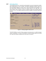
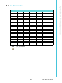
1
User Manual
MIC-3393
6U CompactPCI Intel® Xeon®
Quad/Dual Core Processor Blade
Copyright
The documentation and the software included with this product are copyrighted 2009
by Advantech Co., Ltd. All rights are reserved. Advantech Co., Ltd. reserves the right
to make improvements in the products described in this manual at any time without
notice. No part of this manual may be reproduced, copied, translated or transmitted
in any form or by any means without the prior written permission of Advantech Co.,
Ltd. Information provided in this manual is intended to be accurate and reliable. However, Advantech Co., Ltd. assumes no responsibility for its use, nor for any infringements of the rights of third parties, which may result from its use.
Acknowledgements
All other product names or trademarks are properties of their respective owners.
Product Warranty (2 years)
Advantech warrants to you, the original purchaser, that each of its products will be
free from defects in materials and workmanship for two years from the date of purchase.
This warranty does not apply to any products which have been repaired or altered by
persons other than repair personnel authorized by Advantech, or which have been
subject to misuse, abuse, accident or improper installation. Advantech assumes no
liability under the terms of this warranty as a consequence of such events.
Because of Advantech’s high quality-control standards and rigorous testing, most of
our customers never need to use our repair service. If an Advantech product is defective, it will be repaired or replaced at no charge during the warranty period. For outof-warranty repairs, you will be billed according to the cost of replacement materials,
service time and freight. Please consult your dealer for more details.
If you think you have a defective product, follow these steps:
1. Collect all the information about the problem encountered. (For example, CPU
speed, Advantech products used, other hardware and software used, etc.) Note
anything abnormal and list any onscreen messages you get when the problem
occurs.
2. Call your dealer and describe the problem. Please have your manual, product,
and any helpful information readily available.
3. If your product is diagnosed as defective, obtain an RMA (return merchandise
authorization) number from your dealer. This allows us to process your return
more quickly.
4. Carefully pack the defective product, a fully-completed Repair and Replacement
Order Card and a photocopy proof of purchase date (such as your sales receipt)
in a shippable container. A product returned without proof of the purchase date
is not eligible for warranty service.
5. Write the RMA number visibly on the outside of the package and ship it prepaid
to your dealer.
MIC-3393 User Manual
Part No. 2002339300
Edition 1
Printed in Taiwan
November 2009
ii
Declaration of Conformity
CE
This product has passed the CE test for environmental specifications when shielded
cables are used for external wiring. We recommend the use of shielded cables.
FCC Class A
Note: This equipment has been tested and found to comply with the limits for a Class
A digital device, pursuant to part 15 of the FCC Rules. These limits are designed to
provide reasonable protection against harmful interference when the equipment is
operated in a commercial environment. This equipment generates, uses, and can
radiate radio frequency energy and, if not installed and used in accordance with the
instruction manual, may cause harmful interference to radio communications. Operation of this equipment in a residential area is likely to cause harmful interference in
which case the user will be required to correct the interference at his own expense.
FM
This equipment has passed the FM certification. According to the National Fire Protection Association, work sites are classified into different classes, divisions and
groups, based on hazard considerations. This equipment is compliant with the specifications of Class I, Division 2, Groups A, B, C and D indoor hazards.
Technical Support and Assistance
1.
2.
Visit the Advantech web site at www.advantech.com/support where you can find
the latest information about the product.
Contact your distributor, sales representative, or Advantech's customer service
center for technical support if you need additional assistance. Please have the
following information ready before you call:
– Product name and serial number
– Description of your peripheral attachments
– Description of your software (operating system, version, application software,
etc.)
– A complete description of the problem
– The exact wording of any error messages
iii
MIC-3393 User Manual
Warnings, Cautions and Notes
Warning! Warnings indicate potentially hazardous conditions, which if not
avoided, could cause personal injury!
Caution! Cautions are included to help you avoid damaging hardware or losing
data. e.g.
There is a danger of a new battery exploding if it is incorrectly installed.
Do not attempt to recharge, force open, or heat the battery. Replace the
battery only with the same or equivalent type recommended by the manufacturer. Discard used batteries according to the manufacturer's
instructions.
Note!
Notes provide optional additional information.
Document Feedback
To assist us in making improvements to this manual, we would welcome comments
and constructive criticism. Please send all such - in writing - to:
[email protected]
Packing List
MIC-3393 all-in-one single board computer (CPU heatsink and MCH heatsink
included) x1
! Utility and user manual (PDF file) CD-ROM disc x1
! Daughter board for SATA HDD and HDD tray (Assembled) x 1
! Daughter board for CF x1
! Solder-side cover (Assembled) x1
! RJ45 to DB9 cable x1
! Warranty certificate document x1
If any of these items are missing or damaged, contact your distributor or sales representative immediately.
!
MIC-3393 User Manual
iv
Safety Instructions
1.
2.
3.
Read these safety instructions carefully.
Keep this User Manual for later reference.
Disconnect this equipment from any AC outlet before cleaning. Use a damp
cloth. Do not use liquid or spray detergents for cleaning.
4. For plug-in equipment, the power outlet socket must be located near the equipment and must be easily accessible.
5. Keep this equipment away from humidity.
6. Put this equipment on a reliable surface during installation. Dropping it or letting
it fall may cause damage.
7. The openings on the enclosure are for air convection. Protect the equipment
from overheating. DO NOT COVER THE OPENINGS.
8. Make sure the voltage of the power source is correct before connecting the
equipment to the power outlet.
9. Position the power cord so that people cannot step on it. Do not place anything
over the power cord.
10. All cautions and warnings on the equipment should be noted.
11. If the equipment is not used for a long time, disconnect it from the power source
to avoid damage by transient overvoltage.
12. Never pour any liquid into an opening. This may cause fire or electrical shock.
13. Never open the equipment. For safety reasons, the equipment should be
opened only by qualified service personnel.
14. If one of the following situations arises, get the equipment checked by service
personnel:
– The power cord or plug is damaged.
– Liquid has penetrated into the equipment.
– The equipment has been exposed to moisture.
– The equipment does not work well, or you cannot get it to work according to
the user's manual.
– The equipment has been dropped and damaged.
– The equipment has obvious signs of breakage.
15. DO NOT LEAVE THIS EQUIPMENT IN AN ENVIRONMENT WHERE THE
STORAGE TEMPERATURE MAY GO BELOW -20° C (-4° F) OR ABOVE 60° C
(140° F). THIS COULD DAMAGE THE EQUIPMENT. THE EQUIPMENT
SHOULD BE IN A CONTROLLED ENVIRONMENT.
16. CAUTION: DANGER OF EXPLOSION IF BATTERY IS INCORRECTLY
REPLACED. REPLACE ONLY WITH THE SAME OR EQUIVALENT TYPE
RECOMMENDED BY THE MANUFACTURER, DISCARD USED BATTERIES
ACCORDING TO THE MANUFACTURER'S INSTRUCTIONS.
The sound pressure level at the operator's position according to IEC 704-1:1982 is
no more than 70 dB (A).
DISCLAIMER: This set of instructions is given according to IEC 704-1. Advantech
disclaims all responsibility for the accuracy of any statements contained herein.
v
MIC-3393 User Manual
Safety Precaution - Static Electricity
Follow these simple precautions to protect yourself from harm and the products from
damage.
! To avoid electrical shock, always disconnect the power from your PC chassis
before you work on it. Don't touch any components on the CPU card or other
cards while the PC is on.
! Disconnect power before making any configuration changes. The sudden rush
of power (electrostatic discharge) as you connect a jumper or install a card may
damage sensitive electronic components.
We Appreciate Your Input
Please let us know of any aspect of this product, including the manual, which could
use improvement or correction. We appreciate your valuable input in helping make
our products better.
MIC-3393 User Manual
vi
Contents
Chapter
1
Hardware Configuration......................1
1.1
Introduction ............................................................................................... 2
Table 1.1: MIC-3393 Variants...................................................... 2
Specifications ............................................................................................ 2
1.2.1 CompactPCI Bus Interface ........................................................... 2
1.2.2 CPU .............................................................................................. 3
Table 1.2: Intel processor selection for the MIC-3393................. 3
1.2.3 BIOS ............................................................................................. 3
1.2.4 Chipset.......................................................................................... 3
1.2.5 Memory ......................................................................................... 4
Table 1.3: DDR2 200 Pin Registered SO-RDIMM Tested on the
MIC-3393.................................................................... 4
1.2.6 Ethernet ........................................................................................ 4
Figure 1.1 MIC-3393 Ethernet Ports Configuration ..................... 4
1.2.7 Storage Interface .......................................................................... 5
1.2.8 Serial Interface.............................................................................. 5
1.2.9 USB Port ....................................................................................... 5
1.2.10 LEDs ............................................................................................. 5
1.2.11 Watchdog Timer............................................................................ 5
1.2.12 Optional Rear I/O Modules ........................................................... 6
Table 1.4: RIO-3311 Configurations............................................ 6
1.2.13 Optional Extension Modules ......................................................... 6
Table 1.5: MIC-3312 Configurations............................................ 6
1.2.14 Mechanical and Environmental Specifications.............................. 6
1.2.15 Compact Mechanical Design ........................................................ 7
1.2.16 CompactPCI Bridge ...................................................................... 7
1.2.17 I/O Connectivity............................................................................. 8
1.2.18 Hardware Monitor ......................................................................... 8
1.2.19 Super I/O....................................................................................... 8
1.2.20 RTC and Battery ........................................................................... 8
1.2.21 IPMI............................................................................................... 8
Functional Block Diagram ......................................................................... 9
Figure 1.2 MIC-3393 functional block diagram ............................ 9
Jumpers and Switches .............................................................................. 9
Table 1.6: MIC-3393 jumper descriptions.................................... 9
Table 1.7: MIC-3393 switch descriptions..................................... 9
Figure 1.3 MIC-3393 jumper and switch locations..................... 10
1.4.1 Clear CMOS (JP7) ...................................................................... 10
Table 1.8: JP7 Clear RTC ......................................................... 10
1.4.2 Switch Settings ........................................................................... 11
Table 1.9: SW1 BMC Reset Button & Platform Reset Button ... 11
Table 1.10: SW2-2 & SW4-1 BMC Program or Console ............. 11
Table 1.11: SW3-1 PCI Bridge Master/Drone Mode ................... 11
Table 1.12: SW4 Front COM & RTM COM1/COM2 ports selection
for BMC/SIO UART .................................................. 12
1.4.3 RIO-3311-A1E Switch Setting..................................................... 12
Table 1.13: SW1 External Mini-SAS port/Internal SAS interface 12
1.4.4 MIC-3312-A1E Switch Setting .................................................... 13
Table 1.14: SW1 XMC PCI-Express Selection............................ 13
Connector Definitions.............................................................................. 13
Table 1.15: MIC-3393 connector descriptions............................. 13
Figure 1.4 MIC-3393 Front Panel Ports, Indicators and Buttons14
Figure 1.5 RIO-3311 Front Panel Ports and Indicators ............. 14
1.5.1 USB Connectors ......................................................................... 14
1.2
1.3
1.4
1.5
vii
MIC-3393 User Manual
1.5.2
1.5.3
1.5.4
1.8
1.9
Serial Ports ................................................................................. 14
Ethernet Configuration................................................................ 15
SATA Daughter Board Connector (CNSATA1 and Extension
Module)....................................................................................... 15
1.5.5 System Rest and BMC Reset Button.......................................... 15
1.5.6 VGA Display Connector (Rear I/O)............................................. 15
1.5.7 Mini-SAS Connector (Rear I/O) .................................................. 15
Figure 1.6 SAS Configuration Scenario 1 - Shared Drives........ 15
Figure 1.7 SAS Configuration Scenario 2 - External Drive Array
................................................................................. 16
Figure 1.8 SAS Configuration Scenario 3 - Individual Drives .... 16
1.5.8 XMC / PMC Connectors (Extension Module) ............................. 16
Safety Precautions.................................................................................. 16
Installation Steps..................................................................................... 17
1.7.1 CompactFlash Daughter Board Installation Steps...................... 17
Figure 1.9 Complete assembly of MIC-3393A with SATA HDD
daughter board ......................................................... 17
Figure 1.10Loosen screws on the SATA HDD Daughter Board. 18
Figure 1.11Disassemble SATA HDD Daughter Board and Socket
................................................................................. 18
Figure 1.12Assemble CF Daughter Board ................................. 19
1.7.2 MIC-3312 Extension Board Installation Steps ............................ 20
Figure 1.13Complete assembly of MIC-3393C with MIC-3311-A2E
................................................................................. 20
Figure 1.14Assemble MIC-3312-A1E......................................... 21
Figure 1.15Assemble MIC-3312-A2E......................................... 21
Battery Replacement .............................................................................. 22
Software Support .................................................................................... 22
2
AMI BIOS Setup................................. 23
2.1
Introduction ............................................................................................. 24
Figure 2.1 Setup program initial screen..................................... 24
Entering Setup ........................................................................................ 25
Figure 2.2 Press <DEL> to run setup ........................................ 25
Main Setup.............................................................................................. 26
Figure 2.3 Main setup screen .................................................... 26
2.3.1 System Time/System Date ......................................................... 26
Advanced BIOS Features Setup............................................................. 27
Figure 2.4 Advanced BIOS features setup screen .................... 27
2.4.1 CPU Configuration...................................................................... 28
Figure 2.5 CPU configuration .................................................... 28
2.4.2 LAN Configuration ...................................................................... 29
Figure 2.6 LAN configuration..................................................... 29
2.4.3 IDE Configuration ....................................................................... 30
Figure 2.7 IDE configuration...................................................... 30
2.4.4 Super I/O Configuration .............................................................. 31
Figure 2.8 Super I/O configuration ............................................ 31
2.4.5 Hardware Health Configuration .................................................. 32
Figure 2.9 Hardware health configuration ................................. 32
2.4.6 USB Configuration ...................................................................... 33
Figure 2.10USB configuration .................................................... 33
2.4.7 ACPI Configuration ..................................................................... 34
Figure 2.11ACPI setting ............................................................. 34
Figure 2.12Advanced ACPI configuration .................................. 34
2.4.8 AHCI Configuration..................................................................... 35
Figure 2.13AHCI configuration ................................................... 35
2.4.9 Event Log Configuration ............................................................. 36
Figure 2.14 Event log configuration............................................ 36
1.6
1.7
Chapter
2.2
2.3
2.4
MIC-3393 User Manual
viii
2.5
2.6
2.7
2.8
2.9
Chapter
2.4.10 MPS Configuration...................................................................... 37
Figure 2.15 MPS configuration ................................................... 37
2.4.11 Remote Access Configuration .................................................... 38
Figure 2.16Remote access configuration ................................... 38
2.4.12 Trusting Computing..................................................................... 39
Figure 2.17Console re-direction configuration............................ 39
PCI/PnP Setup ........................................................................................ 40
Figure 2.18PCI/PnP setup .......................................................... 40
2.5.1 Clear NVRAM ............................................................................. 40
2.5.2 Plug and Play O/S....................................................................... 40
2.5.3 PCI Latency Timer ...................................................................... 40
Boot Setup .............................................................................................. 41
Figure 2.19Boot setup ................................................................ 41
2.6.1 Boot Settings Configuration ........................................................ 42
Figure 2.20Boot settings configuration ....................................... 42
Security Setup......................................................................................... 43
Figure 2.21Password configuration ............................................ 43
Advanced Chipset Settings ..................................................................... 44
Figure 2.22Advanced chipset setting.......................................... 44
2.8.1 North Bridge Chipset Configuration ............................................ 45
Figure 2.23North bridge chipset configuration............................ 45
2.8.2 South Bridge Chipset Configuration............................................ 46
Figure 2.24South bridge chipset configuration ........................... 46
Exit Option............................................................................................... 47
Figure 2.25Exit options ............................................................... 47
2.9.1 Save Changes and Exit .............................................................. 47
2.9.2 Discard Changes and Exit .......................................................... 47
2.9.3 Discard Changes ........................................................................ 47
2.9.4 Load Optimal Defaults ................................................................ 47
2.9.5 Load Failsafe Defaults ................................................................ 48
3
IPMI for the MIC-3393 ........................49
3.1
3.2
3.3
Introduction ............................................................................................. 50
Definitions ............................................................................................... 50
IPMI Function List ................................................................................... 50
3.3.1 IPMI Device Global Commands.................................................. 51
Table 3.1: Supported IPMI device global commands ................ 51
3.3.2 BMC Device and Messaging Interfaces...................................... 51
Table 3.2: H8S I2C bus connection to NIC SMBus ................... 51
Table 3.3: NIC interrupt ............................................................. 51
Table 3.4: BMC device and messaging commands .................. 51
3.3.3 BMC Watchdog Timer Commands ............................................. 52
Table 3.5: BMC watchdog timer commands.............................. 52
3.3.4 Event Commands ....................................................................... 52
Table 3.6: Event commands...................................................... 52
3.3.5 PEF and Alerting Commands ..................................................... 52
Table 3.7: PEF and alerting commands .................................... 52
3.3.6 SEL Device Commands.............................................................. 53
Table 3.8: SEL device commands............................................. 53
3.3.7 SDR Device Commands ............................................................. 53
Table 3.9: SDR device commands ............................................ 53
3.3.8 FRU Data .................................................................................... 53
Table 3.10: FRU device commands ............................................ 53
3.3.9 Sensor and Threshold Configuration .......................................... 54
Table 3.11: Sensors list ............................................................... 54
Table 3.12: Threshold values of sensors..................................... 55
Table 3.13: Sensor device commands ........................................ 55
3.3.10 Serial Modem Device Commands .............................................. 55
ix
MIC-3393 User Manual
3.4
Table 3.14: Serial modem device commands ............................. 55
Table 3.15: ................................................................................. 55
Table 3.16: ................................................................................. 55
Table 3.17: ................................................................................. 55
BMC Reset.............................................................................................. 56
Appendix A
Pin Assignments............................... 57
A.1
J1 Connector........................................................................................... 58
Table A.1: J1 CompactPCI I/O .................................................. 58
J2 Connector........................................................................................... 59
Table A.2: J2 CompactPCI I/O .................................................. 59
J3 Connector........................................................................................... 60
Table A.3: J3 CompactPCI I/O (LAN2/LAN3, 2.16) ................... 60
J5 Connector........................................................................................... 61
Table A.4: J5 CompactPCI I/O port ........................................... 61
Other Connectors.................................................................................... 62
Table A.5: CNSATA1 daughter board connector....................... 62
Table A.6: CNSATA1 daughter board connector....................... 62
A.5.1 M/D, PWR, BMC HB, and IDE/Hot-swap LEDs.......................... 62
A.2
A.3
A.4
A.5
Appendix B
Programming the Watchdog Timer . 63
B.1
Watchdog Timer Programming Procedure ............................................. 64
Appendix C
FPGA .................................................. 65
C.1
C.2
Features.................................................................................................. 66
FPGA I/O Registers ................................................................................ 66
Table C.1: LPC I/O registers address ........................................ 66
C.2.1 Debug Message.......................................................................... 66
Table C.2: Debug_Code [7:0] (LPC I/O address: 80H).............. 66
C.2.2 General Control and Status Registers ........................................ 67
C.2.3 General Purpose Registers ........................................................ 70
Watchdog Timer...................................................................................... 71
C.3.1 Initial Watchdog .......................................................................... 71
C.3.2 Program Watchdog..................................................................... 72
C.3
Appendix D
MIC-3393 User Manual
Glossary............................................. 73
x
Chapter
1
1
Hardware
Configuration
This chapter describes how to
configure MIC-3393 hardware.
1.1 Introduction
Using Intel 45nm 64-bit Xeon technology with up to four cores at 2.66GHz combined
with the powerful San Clemente chipset, the MIC-3393 blade boosts computing and
I/O performance deploying the latest virtualization, multi-threading and I/OAT acceleration techniques. Enhanced Xeon packaging, front side bus parity, onboard, soldered DRAM with ECC support and RASUM features integrated in the 5100MCH
combined with PICMG2.9, IPMI-based management make the MIC-3393 a highly
available and reliable high performance computing engine. The comprehensive I/O
subsystem includes an onboard USB flash disk, a 2.5" SATA HDD or CompactFlash
slot, three advanced Gigabit Ethernet controllers, two UARTs, USB ports and a TPM.
The addition of PCIe links to the RTM further enhances versatility compared to previous generation blades resulting in best-in-class connectivity.
The RIO-3311 RTM module supports one PS/2 connector with both keyboard and
mouse ports, three USB ports, two RS-232 ports, 2 SATA ports, a PCIe based server
graphics controller with VGA port, a USB port for USB NAND flash module, and alternate cabling for the three Gigabit Ethernet ports of the MIC-3393. In case the SATA
disk drives and SATA RAID support of the ICH9R do not meet performance and reliability requirements, the RIO-3311 SAS version supports a 4-port SAS controller with
RAID and failover support.
The MIC-3393 is outfitted with single slot (4HP) or dual slot (8HP) front panels to
match CPU performance, CPU power dissipation, and system cooling capabilities.
The 8HP version of the blade can be extended with a MIC-3312 mezzanine module
which can carry two XMCs/PMCs or two 2.5" SATA HDDs to support enhanced I/O
modularity and additional mass storage options.
Table 1.1: MIC-3393 Variants
Features
'A' model Single Slot 'B' model Dual Slots 'C' model Dual Slots
(4HP)
(8HP)
(8HP)
Slot Width
1
2
2
XMC/PMC knockout -
2 (for MIC-3312-A1E) - (not needed for
MIC-3312-A2E)
CPU Heatsink
25mm Height
8mm Height
25mm Height
1.2 Specifications
1.2.1 CompactPCI Bus Interface
The MIC-3393 is compliant with PICMG 2.0 Rev. 3.0. It supports a 64-bit / 66 MHz or
33 MHz PCI bus for up to 8 CompactPCI slots at 3.3 V or 5 V VIO. The MIC-3393 is
hot-swap compliant (PICMG 2.1) and conforms to the CompactPCI Packet Switching
Backplane specification (PICMG 2.16) as well as the CompactPCI System Management Specification (PICMG 2.9).
The board can be configured as a system master or a drone board. In drone mode it
only draws power from the CompactPCI backplane and is not active on the CompactPCI bus. However, PICMG 2.16 is still fully supported in this mode.
MIC-3393 User Manual
2
The MIC-3393 supports the 45nm 64-bit technology Intel Xeon Low Voltage (LV) /
Ultra Low Voltage (ULV) processor family with clock frequencies up to 2.66GHz GHz
and a Front-Side Bus (FSB) up to 1333 MHz.
These processors are validated with the Intel 5100 MCH (San Clemente) chipset.
This chipset provides greater flexibility by deploying the latest virtualization, multithreading and I/OAT acceleration techniques.
Supported processors are listed in the table below. The forced airflow cooling is
required.
Intel CPU
CPU
Advantech PN Model
# cores Freq. Cache FSB
architecture
Number
Required
CPU airflow for
TDP single-slot
width
Required
airflow for
dual-slot
width
96MPXEL5408
2.1FA-12M7T
Harpertown
(45nm)
4
2.13
GHz
12MB 1066 MHz 40W 50CFM
30CFM
96MPXEL5238
2.66FB-6M7T
Wolfdale
(45nm)
2
2.66
GHz
6MB
1333 MHz 35W 40CFM
25CFM
96MPXEL5215
1.86FA-6M7T
Wolfdale
(45nm)
2
1.86
GHz
6MB
1066 MHz 20W 20CFM
15CFM
96MPXE2.4FA-3M7T
Wolfdale
(45nm)
1
2.4
GHz
3MB
1066 MHz 30W 50CFM*
30CFM
L3014
Note!
Strong airflow required for the L3014 CPU is restricted to its thermal
specification (Tc 60°C).
Note!
Because power consumption and thermal restrictions vary between different CompactPCI systems, please double check these items before
installing a higher speed CPU not listed in the table above.
1.2.3 BIOS
Dual 2 MByte SPI flashes contain a board-specific BIOS (from AMI) designed to
meet industrial and embedded system requirements.
1.2.4 Chipset
The Intel 5100 Memory Controller Hub Chipset (Intel 5100 MCH Chipset, formerly
code-named San Clemente) provides excellent flexibility for developers of IT applications by offering high performance Dual-Independent Bus (DIB) and reduced power
consumption using low-power native DDR2 memory. Features include Intel I/O
Acceleration Technology and Intel Virtualization Technology.
The Intel 5100 MCH Chipset, Intel ICH9R I/O controller, and coupled with the energyefficient technology found in Intel's 45nm silicon process enables improved IT application performance with excellent power efficiency and value. It delivers outstanding
system performance through high bandwidth interfaces such as PCI Express, Serial
ATA and Hi-Speed USB 2.0.
3
MIC-3393 User Manual
Hardware Configuration
Table 1.2: Intel processor selection for the MIC-3393
Chapter 1
1.2.2 CPU
1.2.5 Memory
The MIC-3393 has 2GB of on-board ECC DDR2 SDRAM. It also has two 200-pin
SO-DIMM sockets that can accommodate an additional 2GB of memory. The following table shows a list of SORDIMM modules that have been tested on the MIC-3393.
Table 1.3: DDR2 200 Pin Registered SO-RDIMM Tested on the MIC-3393
Advantech PN
Brand
Vendor PN
Size
96SD21G667ER-VI
Virtium
VL493T2863C-E6M
1 GB DDR2 667
(PC2-5300)
128Mb x8
Micron
96SD21G667ER-VI1
Virtium
VL493T2863C-E6S
1 GB DDR2 667
(PC2-5300)
128Mb x8
Samsung
Note!
Speed
Depth / Width Memory Chip
Use of single rank, dual die package stack (3.8mm) SORDIMM is
advised.
1.2.6 Ethernet
The MIC-3393 uses two Intel 82574L LAN controllers to provide 10/100/1000 Mbps
Ethernet connectivity (LAN1/ LAN2 or PICMG2.16) and one Intel 82566DM LAN controller which is an external PHY chip built in ICH9R to provide 10/100/1000 Mbps
Ethernet connectivity (LAN3). Optional settings for the source of the Gigabit Ethernet
ports can be selected in the BIOS menu. These are mutually exclusive and can be
set as:
! LAN1/LAN2 of Front I/O (on the MIC-3393)
! LAN1/LAN2/LAN3 of Rear I/O (on the RTM)
! PICMG 2.16
User can access LAN1 via front panel or rear I/O. LAN2 is accessible via front panel,
rear I/O or PICMG 2.16 on backplane. LAN3 can be connected to rear I/O or PICMG
2.16 on backplane. See figure 1.1 for the configuration.
Figure 1.1 MIC-3393 Ethernet Ports Configuration
MIC-3393 User Manual
4
The MIC-3393 supports five SATA channels. The SATA1 interface can be routed to
an onboard 2.5" SATA hard disk drive or be transferred to access CompactFlash via
SATA-to-IDE daughter board. On-board HDD occupied same space of CF, so each of
them is optional. The SATA2 and STA3 interfaces are routed to the RTM via the J5
connector. The SATA4 and SATA5 are connected to XTM for extra SATA HDDs
request.
Chapter 1
1.2.7 Storage Interface
1.2.8 Serial Interface
1.2.9 USB Port
Seven USB 2.0 compliant ports are provided. Two of them are routed to front panel
connectors; one is routed to an on-board USB flash disk on the MIC-3393. The other
four are routed to the RTM through the J3 connectors, two to the panels of the RTM,
two to the on-board connectors. However, RIO-3311-A1E only supports one onboard USB port due to space limitation.
1.2.10 LEDs
Four LEDs are provided on the front panel as follows:
! One bi-color LED (blue/yellow) indicates hot swap and HDD activity. The blue
color indicates that the board may be safely removed from the system, and the
yellow color indicates HDD activity.
! One LED provides power status. When the LED is green, it means power is provided to the board.
! One LED indicates "Master" or "Drone" mode. The green color stands for "Master” mode. When the LED is off, the board is in "Drone" mode.
! One LED indicates BMC heart beat. When it flashes (yellow), it means the BMC
is active.
1.2.11 Watchdog Timer
An onboard watchdog timer provides system reset capabilities via software control.
The programmable time interval is from 1 to 255 seconds.
5
MIC-3393 User Manual
Hardware Configuration
Two serial ports from SuperIO and one UART from BMC are routed to FPGA to fulfill
several flexible usages. User can access the MIC-3393 or BMC from front or rear
side by setting one DIP switch (SW4). Two serial interfaces are routed to the RTM via
the J3 connector. The other one is designed to serve as a console interface to the
BMC.
1.2.12 Optional Rear I/O Modules
The RIO-3311 is the optional RTM (also known as rear I/O module) for the MIC-3393.
It offers a wide variety of I/O features, such as three RJ45 LAN ports, two COM ports,
one VGA port, two USB2.0 ports, one P/S2 port, and one Mini-SAS port for the RIO3311-A1E model. It also comes with on-board features such as USB2.0, SATA, and
SAS interfaces (SATA pin-headers) for the RIO-3311-A1E model. On the other hand,
the RIO-3311-A2E removes SAS interface, but provides an additional USB2.0 connector for the USB flash module. Rear I/O modules are available with two different I/
O options:
Table 1.4: RIO-3311 Configurations
Rear Panel
RTM
Model
Number
On-board Header/Socket/Connector
SAS
USB
(SATA Slot
LAN COM VGA PS/2* USB MiniSAS USB
SATA
Conn.
Flash**
interfa Width
ce)
RIO-33113
A1E
2
1
1*
2
1
1
-
2
4
1
J1,J3,
J5
RIO-33113
A2E
2
1
1*
2
-
1
1
2
-
1
J1,J3,
J5
Note!
One PS/2 port carries the signals for both K/B and mouse. Y cable is
included.
Note!
Use of Advantech EmbCore USB 2.0 Disk Module Type C is recommended.
1.2.13 Optional Extension Modules
The MIC-3312 is the optional Extension Module (XTM) for the MIC-3393B or the
MIC-3393C, two-slot platform. Extension modules are available with two options:
Table 1.5: MIC-3312 Configurations
XTM Model Number
On-board Header/Socket/Connector
XMC/PMC
SATA HDD
MIC-3312-A1E
2
-
MIC-3312-A2E
-
2
1.2.14 Mechanical and Environmental Specifications
!
Operating temperature: 0 ~ 55°C (-32 ~ 122°F)
Note!
!
The operating temperature range of the MIC-3393 depends on the
installed processor and the airflow through the chassis.
Storage Temperature: -40 ~ 85°„C (-40 ~ 185°„F)
MIC-3393 User Manual
6
1.2.15 Compact Mechanical Design
The MIC-3393 has a specially designed heat sink for the processor to enable fanless
operation. However, forced air cooling in the chassis is still needed for operational
stability and reliability.
1.2.16 CompactPCI Bridge
The MIC-3393 uses a PLX PCI 6540 universal bridge as a gateway to an intelligent
subsystem. When configured as a system controller, the bridge acts as a standard
transparent PCI-X-to-PCI bridge. As a peripheral controller it allows the local
MIC-3393 processor to configure and control the onboard local subsystem independently from the CompactPCI bus host processor. The MIC-3393 local PCI subsystem
is presented to the CompactPCI bus host as a single CompactPCI device. When the
MIC-3393 is in drone mode, the PLX PCI 6540 is electrically isolated from the CompactPCI bus. The MIC-3393 receives power from the backplane, supports rear I/O
and supports PICMG 2.16. The PLX PCI 6540 PCI bridge offers following features:
! PCI Interface
– Full compliance with the PCI Local Bus Specification, Revision 2.3
– Supports 3.3V or 5V tolerance I/O
! Transparent and non-transparent bridge function
! 64-bit, 33MHz/66MHz asynchronous operation
! Support for 8 Bus Masters
! Usable in CompactPCI system slot or peripheral slot
! 10-KB Buffer Architecture for PCI-X-to-PCI-X and PCI-X-to-PCI bridging and
speed conversion
– 1-KB downstream Posted Write buffer
– 1-KB upstream Poster Writer buffer
– 4-KB downstream Read Data buffer
– 4-KB upstream Read Data buffer
Please consult the PLX PCI 6540 data book for details.
7
MIC-3393 User Manual
Hardware Configuration
!
Humidity: 95% @ 40°C (non-condensing)
Humidity (Non-operating): 95% @ 60°C (non-condensing)
Vibration: 5~500Hz, 2Grms
Vibration (Non-operating): 5~500Hz, 3.5Grms
Bump (Non-operating): 15G, 6ms (without on-board 2.5" SATA HDD)
Altitude: up to 4,000m above sea level
Board size:
6U/1 slot width (4HP): 233.35 x 160 x 20 mm (9.2" x 6.3" x 0.8")
6U/2 slot width (8HP): 233.35 x 160 x 40 mm (9.2" x 6.3" x 1.6")
Weight:
6U/1 slot width (4HP): 1.03kg (2.27lb)
6U/2 slot width (8HP): 1.42kg (3.14lb)
Chapter 1
!
!
!
!
!
!
!
1.2.17 I/O Connectivity
For the MIC-3393, the front panel I/O is provided by two RJ-45 Gigabit Ethernet
ports, one RJ-45 COM port and two USB 2.0 ports. Additionally, two XMC/PMC
knockouts for the MIC-3393B model.
Its on-board I/O consists of one SATA channel which can be connected to either a
daughter board for 2.5" SATA HDD, or a SATA-to-IDE daughter board for CompactFlash. Rear I/O connectivity is available via following CompactPCI connectors:
! J3: two Gigabit Ethernet links to the backplane for PICMG 2.16 packet switch,
two COM ports, one PS/2 port (for keyboard/mouse) and six USB ports on the
RTM
! J5: three Gigabit Ethernet LAN ports, one VGA interface, one SAS interface and
two SATA ports on the RTM
1.2.18 Hardware Monitor
One Hardware Monitor (W83627DHG) is available to monitor critical hardware
parameters. It is attached to the BMC to monitor the CPU temperature and core voltage information.
1.2.19 Super I/O
The MIC-3393 Super I/O device provides the following legacy PC devices:
! Serial ports COM1 and COM2 are connected to the rear I/O module or front
panel via two multiplexer in the FPGA.
! The PS2 (keyboard/mouse) is routed to the rear I/O module.
1.2.20 RTC and Battery
The RTC module keeps the date and time. On the MIC-3393 model the RTC circuitry
is connected to battery sources (CR2032M1S8-LF, 3V, 210mAH).
1.2.21 IPMI
The MIC-3393 uses the Intelligent Platform Management Interface (IPMI) to monitor
the health of an entire system. A Renesas H8S/2167 microcontroller provides BMC
functionality to interface between system management software and platform hardware. The MIC-3393 implements fully-compliant IPMI 2.0 functionality and conforms
to the PICMG 2.9 R1.0 specification. The IPMI firmware is based on proven technology from Avocent. Full IPMI details are covered in Chapter 3.
MIC-3393 User Manual
8
Chapter 1
1.3 Functional Block Diagram
1.4 Jumpers and Switches
Table 1.6 and table 1.7 list the jumper and switch functions. Figure 1.3 illustrates the
jumper and switch locations. Read this section carefully before changing the jumper
and switch settings on your MIC-3393 board.
Table 1.6: MIC-3393 jumper descriptions
Number
Function
JP7
Clear CMOS
Table 1.7: MIC-3393 switch descriptions
Number
Function
SW1
BMC Reset/Platform Reset (available on the Front Panel only)
SW2
BMC Firmware Programmable/Console Setting (with SW4
together)
SW3
PCI Bridge Master/Drone Mode
SW4
Front COM & RTM COM1/COM2 ports selection for BMC/SIO
UART, or BMC Firmware Programmable/Console Setting
9
MIC-3393 User Manual
Hardware Configuration
Figure 1.2 MIC-3393 functional block diagram
Figure 1.3 MIC-3393 jumper and switch locations
1.4.1 Clear CMOS (JP7)
This jumper is used to erase CMOS data. Follow the procedures below to clear the
CMOS.
1. Turn off the system.
2. Close jumper JP7 (1-2) for about 3 seconds.
3. Set jumper JP7 back to normal.
4. Turn on the system. The BIOS is reset to its default setting.
Table 1.8: JP7 Clear RTC
Default
MIC-3393 User Manual
Closed
Clear RTC
Open
Normal
10
Note!
! represents the key
Table 1.9: SW1 BMC Reset Button & Platform Reset Button
BMC Reset
SW1-2 (bottom)
Platform Reset
Hardware Configuration
SW1-1 (top)
Table 1.10: SW2-2 & SW4-1 BMC Program or Console
Default
BMC Console
BMC Program
When either front panel COM, RTM COM1 or RTM COM2 is connected to the BMC,
the BMC firmware can be re-programmed by setting switch 2 and switch 4 to "BMC
Program" mode.
Please refer to Table 1.12 for the setting of key 2, 3 and 4 of SW4-1
Table 1.11: SW3-1 PCI Bridge Master/Drone Mode
Default
Master Mode
Drone Mode
11
Chapter 1
1.4.2 Switch Settings
MIC-3393 User Manual
Table 1.12: SW4 Front COM & RTM COM1/COM2 ports selection for BMC/
SIO UART
Default
Front COM for BMC
RTM COM1 for SIO COM1
RTM COM2 for SIO COM2
Front COM for SIO COM1
RTM COM1 for BMC
RTM COM2 for SIO COM2
Front COM for SIO COM2
RTM COM1 for SIO COM1
RTM COM2 for BMC
Please refer to Table 1.10 for the setting of key 1
1.4.3 RIO-3311-A1E Switch Setting
Table 1.13: SW1 External Mini-SAS port/Internal SAS interface
Default
External Mini-SAS 4x Port
Internal SATA ports
1 (SAS Port0)
2 (SAS Port1)
3 (SAS Port2)
4 (SAS Port3)
This switch is only available for the RIO-3311-A1E (supports SAS function) model.
MIC-3393 User Manual
12
Chapter 1
1.4.4 MIC-3312-A1E Switch Setting
Table 1.14: SW1 XMC PCI-Express Selection
Default
XMC1 x8 or PMC x4
XMC2 x8 or PMC x4
Hardware Configuration
XMC1 x8 or PMC x4
XMC2 2 x4 or PMC x4
XMC1 2 x4 or PMC x4
XMC2 x8 or PMC x4
XMC1 2 x4 or PMC x4
XMC2 2 x4 or PMC x4
1.5 Connector Definitions
Table 1.15 lists the function of each connector and Figure 1.4 and 1.5 illustrate each
connector location.
Table 1.15: MIC-3393 connector descriptions
Number
Function
CNSATA1
SATA HDD daughter board / CF daughter board connector
CNXTM1
XTM connector
CNDIMMA1
SORDIMM socket 1
CNDIMMB1
SORDIMM socket 2
CN1
FPGA connector (debug used only)
J1/J2
Primary CompactPCI bus
J3/J5
Rear I/O transition
13
MIC-3393 User Manual
Figure 1.4 MIC-3393 Front Panel Ports, Indicators and Buttons
Figure 1.5 RIO-3311 Front Panel Ports and Indicators
1.5.1 USB Connectors
The MIC-3393 provides up to seven Universal Serial Bus (USB) 2.0 channels. Two
front panel USB ports, CNUSB1 and CNUSB2. One is routed to an on-board USB
flash disk. Four other USB channels are routed to rear I/O via the J3 connector. Two
on the panels, the other two are on-board connectors. However, RIO-3311-A1E only
supports one on-board USB port due to space limitation. The USB interface provides
complete plug and play, hot attach/detach for up to 127 external devices. The MIC3393 USB interface complies with USB specification R2.0 and is fuse protected (5 V
@ 1.1 A). The USB interface can be disabled in the system BIOS setup. The USB
controller default is set to "Enabled".
1.5.2 Serial Ports
The MIC-3393 provides one serial port and the RIO-3311 provides two serial ports.
They are available as RS-232 interfaces via RJ-45 connectors on the front panel. An
RJ-45 to DB-9 adaptor cable is provided in the MIC-3393 accessories to facilitate
connectivity to external console or modem devices. The BIOS Advanced Setup program covered in Chapter 2 provides a user interface for features such as enabling or
disabling the ports and setting the port address. Many serial devices implement the
RS-232 standard in different ways. If you have problems with a serial device, be sure
to check pin assignments on Table 1.12 for the connectors. The IRQ and address
range for these ports are fixed. However, if you wish to disable the port or change
these parameters later, you can do this in the system BIOS setup.
MIC-3393 User Manual
14
The MIC-3393 is equipped with two high performances, PCI-Express based, network
interface controllers which provide fully compliant IEEE802.3 10/100/1000 Mbps
Ethernet interfaces; also one ICH9R built-in PHY chip which also provides 10/100/
1000 Mbps Ethernet interface. Users can choose the LAN1 and LAN2 either via the
front panel RJ-45 connectors or the LAN1, LAN2 and LAN3 on the rear I/O module.
Furthermore, the MIC-3393 supports the PICMG 2.16 Packet Switching Backplane
Specification via the J3 connector.
The MIC-3393 provides one SATA interface via CNSATA1 connector for either a
daughter for SATA HDD, or a SATA-to-IDE daughter board for CompactFlash. Each
one of them is optional as onboard HDD is occupied the same space of CompactFlash. Two SATA interfaces are connected to XTM for extra SATA HDDs request.
MIC-3312-A2E provides two SATA HDD sockets for users who require on-board CF
card and also additional SATA HDDs on the extension module.
1.5.5 System Rest and BMC Reset Button
The MIC-3393 provides a system reset button located on the front panel. The system
reset button resets all payload and application-related circuitry. It does not rest the
system management (IPMI) related circuitry. A separate BMC reset button on the
front panel is provided for the BMC and related hardware.
1.5.6 VGA Display Connector (Rear I/O)
Both RIO-3311-A1E or the RIO-3311-A2E RTM module incorporates the XGI Volari
Z11 GPU, which integrates a PCI-Express 1x controller and a 64-bit 2D graphics
engine. It offers a flexible 16-bit DDR-II memory interface. The Z11 can achieve high
2D performance with a memory interface supporting a bandwidth of up to 1 GB/s
(DDR-II @250MHz). The maximum resolution is 1600 x 1200 at 70 Hz.
1.5.7 Mini-SAS Connector (Rear I/O)
The RIO-3311-A1E provides one SAS interface integrates with a 3.0 Gbit/s SAS/
SATA controller that is compliant with the Fusion-MPT (Message Passing Technology) architecture, provides an eight-lane PCI Express interface, and supports integrated RAID technology. The controller is routed to a x4 mini-SAS connector on the
front panel for a mini-SAS (SFF8088) cable when connecting externally; or to four
on-board SATA Gen. 2 ports by adjusting SW1 switch setting. Figure 1.6, 1.7 and 1.8
describe SAS configurations.
– Blades, RTMs and drives must be
installed in a same chassis
– Two drives shared by two blades
when executing RAID 1
– Use 2pcs 1:2 cable (1x SFF8482,
2x SATA & 1x Power) for internal
connectors
Figure 1.6 SAS Configuration Scenario 1 - Shared Drives
15
MIC-3393 User Manual
Hardware Configuration
1.5.4 SATA Daughter Board Connector (CNSATA1 and Extension
Module)
Chapter 1
1.5.3 Ethernet Configuration
– Connect to external RAID array
– 1pc mini-SAS cable (2x SFF8088)
for external connector
Figure 1.7 SAS Configuration Scenario 2 - External Drive Array
– RIO-3311 connects to one drive
per port
– 1pc 1:1 cable (1x SFF8482, 1x
SATA, 1x Power) for internal connector per drive
Figure 1.8 SAS Configuration Scenario 3 - Individual Drives
1.5.8 XMC / PMC Connectors (Extension Module)
The MIC-3312-A1E XTM supports two PCI Express Mezzanine Cards (XMCs) or PCI
Mezzanine Cards (PMCs). XMCs are connected via two PCI Express x8 buses, and
PMCs are connected via 64-bit / 66 MHz, 3.3V PCI buses. Users can set XMC slots
for either x4 or x8 via SW1 switch setting on the MIC-3312. Front panel accesses are
provided for the XMCs/PMCs that require I/O connectivity.
1.6 Safety Precautions
Follow these simple precautions to protect yourself from harm and the products from
damage.
! To avoid electric shock, always disconnect the power from your CompactPCI
chassis before you work on it. Don't touch any components on the CPU board or
other boards while the CompactPCI chassis is powered.
! Disconnect power before making any configuration changes. The sudden rush
of power as you connect a jumper or install a board may damage sensitive electronic components.
! Always ground yourself to remove any static charge before you touch your CPU
board. Be particularly careful not to touch the chip connectors.
! Modern integrated electronic devices, especially CPUs and memory chips, are
extremely sensitive to electrostatic discharges and fields. Keep the board in its
antistatic packaging when it is not installed in the chassis, and place it on a
static dissipative mat when you are working with it. Wear a grounding wrist strap
for continuous protection.
MIC-3393 User Manual
16
The MIC-3393 contains electrostatically sensitive devices. Please discharge your
body and clothing before touching the assembly. Do not touch components or connector pins. We recommend that you perform assembly at an anti-static workbench.
1.7.1 CompactFlash Daughter Board Installation Steps
Figure 1.9 Complete assembly of MIC-3393A with SATA HDD daughter board
17
MIC-3393 User Manual
Hardware Configuration
The MIC-3393 supports 2.5" SATA hard disk drive or CompactFlash. Either of them is
occupied the same location. The SATA HDD daughter board is assembled on the
MIC-3393, therefore installing a CF daughter board requires removing the SATA
HDD daughter board first. A CF daughter board and four M2.5, 8mm screws are
included as accessories. The following steps illustrate the removal of the SATA HDD
daughter board and the installation of the CF daughter board.
Chapter 1
1.7 Installation Steps
1.
Loosen one M2.5 screw on the center of SATA HDD daughter board and four on
the socket.
Figure 1.10 Loosen screws on the SATA HDD Daughter Board
2.
Remove SATA HDD daughter board and socket
Figure 1.11 Disassemble SATA HDD Daughter Board and Socket
MIC-3393 User Manual
18
Align the CN2 connector of the CF daughter board to the CNSATA1 connector
on the MIC-3393. Then fasten the four M2.5 (8mm) screws, as shown circled in
red in the picture below. The screw circled in blue is used to attach the CF card.
19
MIC-3393 User Manual
Hardware Configuration
Figure 1.12 Assemble CF Daughter Board
Chapter 1
3.
1.7.2 MIC-3312 Extension Board Installation Steps
The MIC-3393B and MIC-3393C support the MIC-3312-A1E and MIC-3312-A2E
extension boards respectively. Following steps illustrate the installation of the extension boards.
Figure 1.13 Complete assembly of MIC-3393C with MIC-3311-A2E
MIC-3393 User Manual
20
Hardware Configuration
Figure 1.14 Assemble MIC-3312-A1E
Figure 1.15 Assemble MIC-3312-A2E
21
Chapter 1
Align the CNXTM1 connector of the MIC-3312 to the CNXTM1 connector on the MIC3393. Then fasten the six M2.5 (4mm) screws in the locations circled in red in Figure
1.14 below for the MIC-3312-A1E; or seven screws in the locations circled in red in
Figure 1.15 for the MIC-3312-A2E.
MIC-3393 User Manual
1.8 Battery Replacement
The Battery model number is CR2032M1S8-LF, a 3V, 210 mAh battery. Replacement
batteries may be purchased from Advantech. When ordering the battery, please contact your local Sales to check availability.
1750129010 - BATTERY 3V/210 mAh with WIRE ASS'Y CR2032M1S8-LF
1.9 Software Support
Windows XP, Windows 2003 and Red Hat Enterprise Linux 5 have been fully tested
on the MIC-3393. Please contact your local sales representative for details on support for other operating systems.
MIC-3393 User Manual
22
Chapter
2
2
AMI BIOS Setup
This chapter describes how to
configure the AMI BIOS.
2.1 Introduction
The AMI BIOS has been customized and integrated into many industrial and embedded motherboards for over a decade. This section describes the BIOS which has
been specifically adapted to the MIC-3393. With the AMI BIOS Setup program, you
can modify BIOS settings and control the special features of the MIC-3393. The
Setup program uses a number of menus for making changes and turning the special
features on or off. This chapter describes the basic navigation of the MIC-3393 setup
screens.
Figure 2.1 Setup program initial screen
The BIOS ROM has a built-in Setup program that allows users to modify the basic
system configuration. This type of information is stored in battery-backed up CMOS
so it retains the Setup information when the power is turned off.
MIC-3393 User Manual
24
Turn on the computer, and there should be a POST (Power-On Self Test) screen that
shows the BIOS supporting the CPU. If there is no number assigned, please contact
an Advantech application engineer to obtain an up-to-date patch code file. This will
ensure that the CPU's system status is valid. After ensuring that you have a number
assigned to the patch code, press <DEL> and you will immediately be allowed to
enter Setup.
Chapter 2
2.2 Entering Setup
AMI BIOS Setup
Figure 2.2 Press <DEL> to run setup
25
MIC-3393 User Manual
2.3 Main Setup
When you first enter the BIOS Setup Utility, you will enter the Main setup screen. You
can always return to the Main setup screen by selecting the Main tab. Two main
setup options are described in this section. The main BIOS setup screen is shown
below.
Figure 2.3 Main setup screen
The main BIOS setup menu screen has two main frames. The left frame displays all
the options that can be configured. "Grayed-out" options cannot be configured whilst
options in blue can. The right frame displays the key legend. Above the key legend is
an area reserved for a text message. When an option is selected in the left frame, it is
highlighted in white. Often a text message will accompany it.
2.3.1 System Time/System Date
Use this option to change the system time and date. Highlight System Time or System Date using the <Arrow> keys. Enter new values through the keyboard. Press the
<Tab> key or the <Arrow> keys to move between fields. The date must be entered in
MM/DD/YY format. The time is entered in HH:MM:SS format.
MIC-3393 User Manual
26
Select the Advanced tab from the MIC-3393 setup screen to enter the Advanced
BIOS Setup screen. You can select any of the items in the left frame of the screen,
such as CPU Configuration, to go to the sub menu for that item. You can display an
Advanced BIOS Setup option by highlighting it using the <Arrow> keys. All Advanced
BIOS Setup options are described in this section. The Advanced BIOS Setup screen
is shown below. The sub menus are described on the following pages.
Chapter 2
2.4 Advanced BIOS Features Setup
AMI BIOS Setup
Figure 2.4 Advanced BIOS features setup screen
27
MIC-3393 User Manual
2.4.1 CPU Configuration
Figure 2.5 CPU configuration
2.4.1.1 Intel Virtualization Tech
This BIOS feature is used to enable or disable the Intel Virtualization Technology
(IVT) extensions that allow multiple operating systems to run simultaneously on the
same system. It does this by creating virtual machines, each running its own x86
operating system. The default setting for this item is set to "Enabled".
2.4.1.2 PECI
This item specifies the Platform Environment Control Interface. The default setting for
this item is set to "Enabled".
2.4.1.3 Intel SpeedStep Tech
This item allows the processor to meet the instantaneous performance needs of the
operation being performed, while minimizing power draw and heat dissipation. The
default setting is "Enabled".
MIC-3393 User Manual
28
Chapter 2
2.4.2 LAN Configuration
AMI BIOS Setup
Figure 2.6 LAN configuration
2.4.2.1 Select LAN1 mode
Two options are available: Front or RTM. Used to select LAN1 connect to either RJ45 LAN port on front panel or rear I/O. The default setting for this item is set to
"Front".
2.4.2.2 Select LAN2 mode
Three options are available: Front, RTM or PICMG 2.16. Used to select LAN2 connect to either RJ-45 LAN port on front panel, RJ-45 LAN port on rear I/O or backplane
via PICMG 2.16. The default setting for this item is set to "Front".
2.4.2.3 Select LAN3 mode
Two options are available: RTM or PICMG 2.16. Used to select LAN3 connect to
either RJ-45 LAN port on rear I/O or backplane via PICMG 2.16. The default setting
for this item is set to "RTM".
29
MIC-3393 User Manual
2.4.3 IDE Configuration
Figure 2.7 IDE configuration
2.4.3.1 SATA#1 Configuration
Three options are available: Disabled, Compatible or Enhanced. "Disabled" means
that all SATA resources are disabled. "Compatible" enables up to two SATA channels
for OS's requiring legacy IDE operation (default setting). And, "Enhanced" enables all
SATA resources. The default setting is "Compatible".
2.4.3.2 Configure SATA#1 as
Three options are available: "IDE", "RAID" and "AHCI". The default setting is "IDE".
2.4.3.3 SATA#2 Configuration
Two options are available: Disabled or Enhanced. The default setting is "Enhanced".
2.4.3.4 Primary/Secondary/Third/Fourth IDE Master and Slave
While entering setup, BIOS auto detects the presence of IDE devices. This displays
the status of auto detection of four possible IDE devices.
2.4.3.5 Hard Disk Write Protect
Disable or enable device write protection. Enable effectively only if device is
accessed through BIOS. This option only functions under DOS. The default setting
for this item is set to "Disabled".
2.4.3.6 IDE Detect Time Out (Sec)
Select the time out value for detecting ATA/ATAPI devices. The default setting for this
item is set to "35".
MIC-3393 User Manual
30
Chapter 2
2.4.4 Super I/O Configuration
AMI BIOS Setup
Figure 2.8 Super I/O configuration
2.4.4.1 Serial Port1/2 Address
Used to select Serial Port1 / Serial Port2 base addresses.
31
MIC-3393 User Manual
2.4.5 Hardware Health Configuration
Figure 2.9 Hardware health configuration
System temperature, CPU temperature, VTIN temperature and voltage status are
displayed in the Hardware Health Configuration.
MIC-3393 User Manual
32
Chapter 2
2.4.6 USB Configuration
AMI BIOS Setup
Figure 2.10 USB configuration
2.4.6.1 Legacy USB Support
Enable support for legacy USB. Auto option disables legacy support if no USB device
is connected. The default setting for this item is set to "Enabled".
2.4.6.2 USB 2.0 Controller Mode
Configure the USB 2.0 controller in HiSpeed (480Mbps) or FullSpeed (12Mbps). The
default setting for this item is set to "HiSpeed".
2.4.6.3 USB EHCI Hand-Off
This is a workaround for OS without EHCI hand-off support. The EHCI ownership
change should claim by EHCI driver. The default setting for this item is set to
"Enabled".
2.4.6.4 USB Write Protect
Disable or enable device write protection. Enable effective only if device is accessed
through BIOS. The default setting for this item is set to "Enabled".
33
MIC-3393 User Manual
2.4.7 ACPI Configuration
Figure 2.11 ACPI setting
2.4.7.1 Advanced ACPI Configuration
Use this section to configure additional ACPI options.
Figure 2.12 Advanced ACPI configuration
2.4.7.2 ACPI Aware O/S
ACPI puts power management in the hands of the operating system. The options for
"ACPI Aware O/S" are "Yes" or "No" in order to enable or disable ACPI support for
the operating system. The default setting is "Yes".
2.4.7.3 ACPI APIC Support
Enable or disable ACPI APIC table pointer to RSDT pointer list. The default setting is
"Enabled.
2.4.7.4 AMI OEMB Table
Enable or disable OEMB table pointer to R(X)SDT pointer list. The default setting is
"Enabled".
MIC-3393 User Manual
34
Chapter 2
2.4.8 AHCI Configuration
2.4.8.1 AHCI BIOS Support
Enable or disable Advanced Host Controller Interface (AHCI) support. AHCI allows
the storage driver to enable advanced Serial ATA features such as Native Command
Queuing and hot plug. The default setting is "Enabled".
2.4.8.2 AHCI CD/DVD Boot Time out
Select the time out value for AHCI CD/DVD Boot devices. The default setting for this
item is set to "35".
35
MIC-3393 User Manual
AMI BIOS Setup
Figure 2.13 AHCI configuration
2.4.9 Event Log Configuration
Figure 2.14 Event log configuration
2.4.9.1 ECC Event Logging
You can enable or disable ECC Event Logging. The default setting is "Enabled".
MIC-3393 User Manual
36
Chapter 2
2.4.10 MPS Configuration
2.4.10.1 MPS Revision
MPS allows the BIOS to configure the Multi-Processor Specification revision level.
Some operation systems will require revision 1.1 for compatibility reasons. The
default setting is "1.4".
37
MIC-3393 User Manual
AMI BIOS Setup
Figure 2.15 MPS configuration
2.4.11 Remote Access Configuration
Figure 2.16 Remote access configuration
2.4.11.1 Remote Access
You can disable or enable the BIOS remote access feature here. The default setting
is "Enabled".
2.4.11.2 Serial Port Number
Select the serial port you want to use for console redirection. You can set the value
for this option to either SIO COM1 or COM2. The default setting is SIO COM1.
2.4.11.3 Serial Port Mode
Select the baud rate you want to use for console redirection. The default setting is
"115200 8, n, 1".
2.4.11.4 Flow Control
Select Flow Control for console redirection. The default setting is "None".
2.4.11.5 Redirection after BIOS POST
Three options are available: Disabled, Boot Loader or Always. "Disabled" will turn off
the redirection after POST. "Boot Loader" means that redirection is active during
POST and during boot loader. And, "Always" means that redirection is always active.
However, some OS may not work even set to Always.
2.4.11.6 Terminal Type Combo Key Support
Select the target terminal type.
2.4.11.7 VT-UTF8
Enable or disable VT-UTF8 combination key support for ANSI/VT100 terminals.
2.4.11.8 Serial Over LAN
Enable or disable Serial over LAN (SOL) function. The default setting is "Disabled".
MIC-3393 User Manual
38
Chapter 2
2.4.12 Trusting Computing
2.4.12.1 TCG/TPM Support
Enable or disable TPM TCG (TPM 1.1/1.2) support in BIOS.
2.4.12.2 Execute TPM Command
Three options are available: "Don't change", "Disabled" or "Enabled". The default setting, "Don't Change" keeps TPM command to initial setting.
39
MIC-3393 User Manual
AMI BIOS Setup
Figure 2.17 Console re-direction configuration
2.5 PCI/PnP Setup
Select the PCI/PnP tab from the MIC-3393 setup screen to enter the Plug and Play
BIOS Setup screen. You can display a Plug and Play BIOS Setup option by highlighting it using the <Arrow> keys. All Plug and Play BIOS Setup options are described in
this section. The Plug and Play BIOS Setup screen is shown below.
Figure 2.18 PCI/PnP setup
2.5.1 Clear NVRAM
Set this value to force the BIOS to clear the Non-Volatile Random Access Memory
(NVRAM) during system boot. The default setting is "No".
2.5.2 Plug and Play O/S
Select "No" to let the BIOS configure all the devices in the system. Select "YES" will
let the operating system configure Plug and Play (Pnp) devices that are not required
for boot if your system has a Plug and Play operating system. The default setting is
"No".
2.5.3 PCI Latency Timer
This option sets the latency of all PCI devices on the PCI bus. The default setting is
64.
MIC-3393 User Manual
40
Chapter 2
2.6 Boot Setup
AMI BIOS Setup
Figure 2.19 Boot setup
Note!
"Hard Disk Drives" will only appear on the setup screen when at least
one hard disk drive is connected to the MIC-3393.
41
MIC-3393 User Manual
2.6.1 Boot Settings Configuration
Figure 2.20 Boot settings configuration
2.6.1.1 Quick Boot
Allow BIOS to skip certain tests while booting. The system Configure Summary will
be skipped. This will decrease the time needed to boot the system. The default setting is on "Enabled".
2.6.1.2 Quiet Boot
Used to display OEM logo when the setting is "Enabled". The default setting, "Disabled", displays normal POST message.
2.6.1.3 Wait For 'F1' If Error
Wait for the F1 key to be pressed if an error occurs.
2.6.1.4 Interrupt 19 Capture
Allow option ROMs to trap interrupt 19. This is required by some PCI cards that provide a ROM based setup utility.
MIC-3393 User Manual
42
Chapter 2
2.7 Security Setup
AMI BIOS Setup
Figure 2.21 Password configuration
Select Security Setup from the MIC-3393 Setup main BIOS setup menu. All Security
Setup options, such as password protection and virus protection, are described in
this section. To access the sub menu for the following items, select the item and
press <Enter>:
! Change Supervisor Password
! Change User Password
43
MIC-3393 User Manual
2.8 Advanced Chipset Settings
Figure 2.22 Advanced chipset settings
MIC-3393 User Manual
44
Chapter 2
2.8.1 North Bridge Chipset Configuration
2.8.1.1 Hyper-Threading Function
Enable or disable Hyper-Threading functionality.
2.8.1.2 Crystal Beach / DMA
Enable or disable Crystal Beach / DMA configuration.
2.8.1.3 MCH Channel Mode
Select Channel Sequencing to allocate address channel - then 1. Select Channel
Interleave to interleave channel across channels. Select Single Channel 0 to force
single channel 0. The default setting is "Channel Interleave".
2.8.1.4 Patrol Scrubbing
Enable or disable ECC patrol scrub.
2.8.1.5 Demand Scrubbing
Enable or disable ECC demand scrub.
2.8.1.6 Channel Dependent Sparing
Enable or disable Channel-dependent rank/DIMM sparing.
2.8.1.7 Channel 0/1
Enable or disable Channel 0/1.
2.8.1.8 Channel Specific Sparing
Enable or disable rank/DIMM sparing feature of Channel 0/Channel 1.
2.8.1.9 Rank Interleaving
The default setting of Channel 0/Channel 1 is "4:1".
2.8.1.10 Dynamic Calibration
This feature allows for the memory interface to calibrate quickly by using the stored
calibration data from a previous power on. If enabled, CMOS must be cleared when
memory configuration changes.
2.8.1.11 Boots Graphic Adapter Priority
Select which graphics controller to use as the primary boot device. Two options are
available: "Auto" or "Onboard VGA". Select "Auto", the external graphics card will be
set as first priority. Select "Onboard VGA" to boot graphics from RTM only.
2.8.1.12 Read Completion Coalescing
The default setting of this item is "Auto".
45
MIC-3393 User Manual
AMI BIOS Setup
Figure 2.23 North Bridge chipset configuration
2.8.2 South Bridge Chipset Configuration
Figure 2.24 South Bridge chipset configuration
2.8.2.1 USB Functions
The default setting is "12 USB Ports".
2.8.2.2 USB Port Configure
The default setting is "6X6 USB Ports"
2.8.2.3 SMBUS Controller
The default setting is "Enabled"
2.8.2.4 Spectrum Mode
The default setting is "Enabled"
MIC-3393 User Manual
46
Chapter 2
2.9 Exit Options
AMI BIOS Setup
Figure 2.25 Exit options
2.9.1 Save Changes and Exit
When you have completed the system configuration changes, follow these steps:
1. Select Exit Saving Changes from the Exit menu and press <Enter>. The following messages appear on the screen:
Save Configuration Changes and Exit Now?
[Ok] [Cancel]
2. Select "Ok" to save changes and exit.
2.9.2 Discard Changes and Exit
Follow these steps to quit Setup without making any permanent changes to the system configuration.
1. Select Exit Discarding Changes from the Exit menu and press <Enter>. The following messages appear on the screen:
Discard Changes and Exit Setup Now?
[Ok] [Cancel]
2. Select "Ok" to discard changes and exit. The following messages appear on the
screen:
Discard Changes
3. Select "Discard Changes" from the Exit menu and press <Enter>.
2.9.3 Discard Changes
Discard changes done so far to any of the setup questions.
2.9.4 Load Optimal Defaults
This loads the optimal defaults values for the MIC-3393 which allows optimum functionality and system performance. Select "Load Optimal Defaults" from the Exit menu
and press <Enter>.
47
MIC-3393 User Manual
2.9.5 Load Failsafe Defaults
This loads the basic defaults values for the MIC-3393 which may not work best for all
computer applications. Select "Load Failsafe Defaults" from the Exit menu and press
<Enter>.
MIC-3393 User Manual
48
Chapter
3
3
IPMI for the MIC-3393
This chapter describes IPMI configuration for the MIC-3393.
3.1 Introduction
The MIC-3393 fully supports the IPMI 2.0 interface and the PICMG 2.9 R1.0 specification. The Renesas H8S/2167 has been implemented as the IPMI controller / Baseboard Management Controller (BMC) to run firmware and collect information. The
MIC-3393 IPMI firmware is sourced from Avocent, a provider of proven and tested
IPMI implementations in a wide range of mission-critical applications. The BMC's key
features and functions are listed below.
! Compliant with IPMI specification, revision 2.0
! Compliant with PICMG 2.9 specification
! Environment monitoring (temperature and voltage)
! Power/Reset control via IPMI chassis command
! Complete SEL, SDR and FRU functionality
! FRU data capacity: 2 KB
! Provides 4 messaging interfaces
! One serial port
! One LPC interface
! One IPMB channel
! One LAN channel messaging via sideband NIC for out-of-band management
! Four I2C buses (including IPMB and SMBus) and two optional others
! Firmware Hub flashing and updating over serial port
! One hardware monitor
! One interrupt input
! Sensors threshold configuration
! Complete IPMI watchdog functionality (reset, power down, power cycle)
! Platform even filtering (PEF) and alert policies
! External Event Generation
3.2 Definitions
!
!
!
!
BMC - (Baseboard Management Controller): This is the common abbreviation for an IPMI Baseboard Management Controller.
IPMB - (Intelligent Platform Management Bus): A protocol defined for passing IPMI messages over a public I2C bus.
IPMI - (Intelligent Platform Management Interface): A standardized system
management interface. Please refer to the IPMI Specification for more details.
IPMIv2.0: Specifically version 2.0 of IPMI
3.3 IPMI Function List
The following standard IPMI commands are supported.
Note!
The Network function (NetFn) field identifies the functional class of the
message. The Network Function clusters IPMI commands into different
sets. Please refer to the IPMI specification of network function codes for
more information.
These command codes are compliant with the IPMI specification. Mandatory and
Optional commands are defined in the IPMI specification.
For more details, please refer to the IPMI specification.
MIC-3393 User Manual
50
Table 3.1: Supported IPMI device global commands
NetFn
Cmd
Mandatory/Optional
Get Device Id
App
0x01
M
Cold Reset
App
0x02
O
Get Self Test Results
App
0x04
M
Manufacturing Test On
App
0x05
O
Set ACPI Power State
App
0x06
O
Get ACPI Power State
App
0x07
O
3.3.2 BMC Device and Messaging Interfaces
The BMC messaging interfaces comply with the Intelligent Platform Management
Interface Specification, Version 2.0. The MIC-3393 provides 4 messaging interface
channels.
! LPC/KCS channel: Connects the H8S/2167 to the system LPC bus. Firmware
sets 1 host interface over LPC: KCS for SMS.
! IPMB channel: Connects IPMB devices or connects to the H8S/2167's I2C_0
interface.
! Serial port: The H8S/2167 supports one serial port for out-of-band management (OOB) as well as one serial port for firmware flash update. Serial Port 0 is
selected for OOB serial port
! LAN channel: OOB management over LAN is accomplished by a sharing a NIC
(LAN3). This messaging interface channel connects the H8S/2167's I2C interface to the NIC's SMBus interface.
Table 3.2: H8S I2C bus connection to NIC SMBus
I2C_1
H8S/2167 Pin Name I2C address
Pin Number
System Connection
SCL1
48
NIC SMBus clock
47
NIC SMBus data
0xC6
SDA1
Table 3.3: NIC interrupt
H8S/2167 Pin Name
Pin Number
Usage
IRQ1#
130
SMALERT# for NIC SMBus
Table 3.4: BMC device and messaging commands
BMC Device and Messaging Commands
NetFn
Cmd
Mandatory/Optional
Set BMC Global Enables
App
0x2e
M
Get BMC Global Enables
App
0x2f
M
Clear Message Flags
App
0x30
M
Get Message Flags
App
0x31
M
Enable Message Channel Receive
App
0x32
O
Get Message
App
0x33
M
Send Message
App
0x34
M
51
MIC-3393 User Manual
IPMI for the MIC-3393
IPMI Device Global Commands
Chapter 3
3.3.1 IPMI Device Global Commands
Table 3.4: BMC device and messaging commands
Read Event Message Buffer
App
0x35
O
Get System GUID
App
0x37
O
Set Channel Access
App
0x40
O
Get Channel Access
App
0x41
O
Get Channel Info
App
0x42
O
Set User Access
App
0x43
O
Get User Access
App
0x44
O
Set User Name
App
0x45
O
Get User Name
App
0x46
O
Set User Password
App
0x47
O
Master Write-Read
App
0x52
M
3.3.3 BMC Watchdog Timer Commands
Table 3.5: BMC watchdog timer commands
BMC Watchdog Timer Commands
NetFn
Cmd
Mandatory/Optional
Reset Watchdog Timer
App
0x22
M
Set Watchdog Timer
App
0x24
M
Get Watchdog Timer
App
0x25
M
3.3.4 Event Commands
Table 3.6: Event commands
Event Command
NetFn
Cmd
Mandatory/Optional
Set Event Receiver
S/E
0x00
M
Get Event Receiver
S/E
0x01
M
3.3.5 PEF and Alerting Commands
Table 3.7: PEF and alerting commands
PEF and Alerting Command
NetFn
Cmd
Mandatory/Optional
Get PEF Capabilities
S/E
0x10
M
Arm PEF Postpone Timer
S/E
0x11
M
Get PEF Configuration Parameters
S/E
0x13
M
Set Last Processed Event ID
S/E
0x14
M
Get Last Processed Event ID
S/E
0x15
M
MIC-3393 User Manual
52
Table 3.8: SEL device commands
SEL Device Command
NetFn
Cmd
Mandatory/Optional
Get SEL Info
Storage
Storage 0x40
M
Storage
Storage 0x42
O
Get SEL Entry
Storage
Storage 0x43
M
Get SEL Time
Storage
Storage 0x48
M
Set SEL Time
Storage
Storage 0x49
M
3.3.7 SDR Device Commands
Table 3.9: SDR device commands
SDR Device Command
NetFn
Cmd
Mandatory/Optional
Get SDR Repository Info
Storage
0x20
M
Reserve SDR Repository
Storage
0x22
M
Get SDR
Storage
0x23
M
Get SDR Repository Time
Storage
0x28
M
Set SDR Repository Time
Storage
0x29
M
Run Initialization Agent
Storage
0x2c
O
3.3.8 FRU Data
The MIC-3393 supports the IPMI FRU function to store accessible multiple sets of
non-volatile Field Replaceable Unit (FRU) information in FRU EEPROM. The FRU
data includes information such as serial number, part number, model, and asset tag.
FRU information is accessed using IPMI commands compliant to the IPMI 2.0 specification as below.
Table 3.10: FRU device commands
FRU Device Command
NetFn
Cmd
Mandatory/Optional
Get FRU Inventory Area Info
Storage
0x10
M
Read FRU Inventory Data
Storage
0x11
M
Write FRU Inventory Data
Storage
0x12
M
53
MIC-3393 User Manual
IPMI for the MIC-3393
Reserve SEL
Chapter 3
3.3.6 SEL Device Commands
3.3.9 Sensor and Threshold Configuration
Sensor data record (SDR) repository will be stored in BMC's flash memory and cannot be changed.
Note!
UNC = Upper Non-Critical.
UC = Upper Critical
UNR = Upper Non-Recoverable
LNC = Lower Non-Critical
LC = Lower Critical
LNR = Lower Non-Recoverable
Table 3.11: Sensors list
Sensor Name
Power Unit Status
Reading
Sensor Sensor
Logged
Type
Logged Assertions
Number Type
De-assertions
Sensor
50h
09h
6Fh
00h - Power Off
00h - Power Off
04h - AC Lost
51h
23h
00h - Timer Expired,
status only
6Fh
01h - Hard Reset
Watchdog
N/A
02h - Power Down
03h - Power Cycle
Power Failure
52h
C0h
6Fh
00h - Power Failure
00h - Power Failure
07h - over 75% full
SEL Full
64h
D0h
01h
09h - over 90% full
N/A
0Bh - 100% full
W83627HG Temp 00h
01h
01h
UNC, UNR
UNC, UNR
W83627HG 3.3V
01h
02h
01h
LC, UC
LC, UC
W83627HG 2.5V
02h
02h
01h
LC, UC
LC, UC
W83627HG 5V
03h
02h
01h
LC, UC
LC, UC
W83627HG 12V
04h
02h
01h
LC, UC
LC, UC
W83627HG VCC
05h
02h
01h
LNC,UC
LNC,UC
Note!
A chassis intruder sensor is not used on the MIC-3393 platform.
Power failure sensor type "C0h" indicates a power failure event.
Apart from the following list of sensors, other sensors should be reinitialized when the system is powered on or reset.
- VCC
- SEL Fullness
- System PWR monitor
- Watchdog
MIC-3393 User Manual
54
Sensor Entity
Nominal UNR UC
Number Instance Reading
10h
01h
1.2 V
UNC LNR LC
LNC Positive- Negativegoing
going
N/A
1.44 V N/A
N/A
0.8 V
N/A 0x02
0x02
01h
1.2 V
N/A
1.44 V N/A
N/A
0.8 V
N/A 0x02
0x02
12h
01h
3.3 V
N/A
3.63 V N/A
N/A
2.97 V N/A 0x02
0x02
13h
01h
12 V
N/A
13.2 V N/A
N/A
10.8 V N/A 0x02
0x02
14h
01h
1.8 V
N/A
1.98 V N/A
N/A
1.62 V N/A 0x02
0x02
15h
01h
5V
N/A
5.5 V
N/A
N/A
4.5 V
N/A 0x02
0x02
16h
01h
3.3 V
N/A
3.63 V N/A
N/A
2.97 V N/A 0x02
0x02
20h
01h
35 C
55 C 50 C
N/A
N/A
N/A
N/A 0x02
0x02
21h
01h
70 C
N/A
100 C N/A
N/A
N/A
N/A 0x02
0x02
Table 3.13: Sensor device commands
Sensor Device Command
NetFn
Cmd
Mandatory/Optional
Set Sensor Hysteresis
S/E
0x24
O
Get Sensor Hysteresis
S/E
0x25
O
Set Sensor Threshold
S/E
0x26
O
Get Sensor Threshold
S/E
0x27
O
Set Sensor Event Enable
S/E
0x28
O
Get Sensor Event Enable
S/E
0x29
O
Re-arm Sensor Events
S/E
0x2a
O
Get Sensor Event Status
S/E
0x2b
O
Get Sensor Reading
S/E
0x2d
M
3.3.10 Serial Modem Device Commands
Table 3.14: Serial modem
device commands
Table 3.15: Table3.16: Table 3.17:
Serial Modem Device Command
NetFn
Cmd
Mandatory/Optional
Set serial modem configuration
parameters
Transport
0x10
M
Get Serial Modem Configuration
Parameters
Transport
0x11
M
Set Serial Modem Mux
Transport
0x12
M
55
MIC-3393 User Manual
IPMI for the MIC-3393
11h
Chapter 3
Table 3.12: Threshold values of sensors
3.4 BMC Reset
The BMC can initiate a graceful shutdown of the MIC-3393 by issuing a short pulse
(~500 ms) on the power button signal to the ACPI controller when commanded
through its host, OOB, or IPMB channels as well as from a Graceful Shutdown Event
from the CMM or a Handle OPEN event. An ACPI compliant OS will then perform a
graceful shutdown and light the blue LED whereas a non-compliant OS will just shut
down.
Note!
The Network function (NetFn) field identifies the functional class of the
message. The Network Function clusters IPMI commands into different
sets. Please refer to the IPMI specification of network function codes for
more information.
These command codes are compliant with the IPMI specification.
Mandatory and Optional commands are defined in the IPMI specification.
For more details, please refer to the IPMI specification.
MIC-3393 User Manual
56
Appendix
A
A
Pin Assignments
This appendix describes pin
assignments.
A.1 J1 Connector
Table A.1: J1 CompactPCI I/O
Pin
Z
A
B
C
D
E
F
25
GND
5V
REQ64#
ENUM#
3.3V
5V
GND
24
GND
AD(1)
5V
V(I/O)
AD(O)
ACK64#
GND
23
GND
3.3V
AD(4)
AD(3)
5V
AD(2)
GND
22
GND
AD(7)
GND
3.3V
AD(6)
AD(5)
GND
21
GND
3.3V
AD(9)
AD(8)
M66EN(3) C/BE(0)#
GND
20
GND
AD(12)
GND
V(I/O)
AD(11)
AD(10)
GND
19
GND
3.3V
AD(15)
AD(14)
GND
AD(13)
GND
18
GND
SERR#
GND
3.3V
PAR
C/BE(1)#
GND
17
GND
3.3V
IPMB_SCL
IPMB_SDA
GND
PERR#
GND
16
GND
DEVSEL#
GND
V(I/O)
STOP#
LOCK#
GND
15
GND
3.3V
FRAME#
IRDY#
BD_SEL# TRDY#
GND
12-14
KEY AREA
11
GND
AD(18)
AD(17)
AD(16)
GND
C/BE(2)#
GND
10
GND
AD(21)
GND
3.3V
AD(20)
AD(19)
GND
9
GND
C/BE(3)#
IDSEL
AD(23)
GND
AD(22)
GND
8
GND
AD(26)
GND
V(I/O)
AD(25)
AD(24)
GND
7
GND
AD(30)
AD(29)
AD(28)
GND
AD(27)
GND
6
GND
REQ0#
PRESENT#
3.3V
CLK0
AD(31)
GND
5
GND
NC
NC
RST#
GND
GNT0#
GND
4
GND
IPMB_PWR
HEALTHY#
V(I/O)
INTP
INTS
GND
3
GND
INTA#
INTB#
INTC#
5V
INTD#
GND
2
GND
NC
5V
NC
NC
NC
GND
1
GND
5V
£¦12V
NC
£´12V
5V
GND
Pin
Z
A
B
C
D
E
F
Note!
NC: No Connect
#: Active Low
MIC-3393 User Manual
58
Table A.2: J2 CompactPCI I/O
Pin
Z
A
B
C
D
E
F
22
GND
GA4
GA3
GA2
GA1
GA0
GND
21
GND
CLK6
GND
NC
NC
NC
GND
20
GND
CLK5
NC
NC
GND
NC
GND
19
GND
NC
GND
SMB_SDA
SMB_SCL
SMB_ALERT
GND
18
GND
NC
NC
NC
GND
NC
GND
17
GND
NC
GND
PRST
REQ6#
GNT6#
GND
16
GND
NC
NC
DEG#
GND
NC
GND
15
GND
NC
GND
FAL#
REQ5#
GNT5#
GND
14
GND
AD(35)
AD(34)
AD(33)
GND
AD(32)
GND
13
GND
AD(38)
GND
V(I/O)
AD(37)
AD(36)
GND
12
GND
AD(42)
AD(41)
AD(40)
GND
AD(39)
GND
11
GND
AD(45)
GND
V(I/O)
AD(44)
AD(43)
GND
10
GND
AD(49)
AD(48)
AD(47)
GND
AD(46)
GND
9
GND
AD(52)
GND
V(IO)
AD(51)
AD(50)
GND
8
GND
AD(56)
AD(55)
AD(54)
GND
AD(53)
GND
7
GND
AD(59)
GND
V(IO)
AD(58)
AD(57)
GND
6
GND
AD(63)
AD(62)
AD(61)
GND
AD(60)
GND
5
GND
C/BE(5)#
GND
V(I/O)
C/BE(4)#
PAR64
GND
4
GND
V(I/O)
NC
C/BE(7)
GND
C/BE(6)#
GND
3
GND
CLK4
GND
GNT3#
REQ4#
GNT4#
GND
2
GND
CLK2
CLK3
SYSEN#(2)
GNT2#
REO3#
GND
1
GND
CLK1
GND
REO1#
GNT1#
REO2#
GND
Note!
NC: No Connect
#: Active Low
59
MIC-3393 User Manual
Appendix A Pin Assignments
A.2 J2 Connector
A.3 J3 Connector
Table A.3: J3 CompactPCI I/O (LAN2/LAN3, 2.16)
Pin F
A
B
C
D
E
Z
1
GND VCC
VCC
VCC
VCC
USB_OC4#
GND
2
GND VCC
VCC
VCC
VCC
USB_P4+
GND
3
GND GND
GND
GND
GND
USB_P4-
GND
4
GND COM1_RX#
COM1_CTS# GND
COM2_TX#
USB_OC5#
GND
5
GND COM1_TX#
COM1_DSR# COM2_DCD# COM2_DTR# USB_P5+
6
GND COM1_RTS# COM1_DTR# COM2_RTS# COM2_RI#
7
GND COM1_DCD# COM1_RI#
8
GND USB_OC9#
USB_OC10# COM2_DSR# TBD/TMS
9
GND USB_P9-
USB_P10-
USB_P6-
GND
10
GND USB_P9+
USB_P10+
TBD/TDO
TBD/TRST#
USB_OC7#
GND
11
GND GND
GND
NC
NC
USB_P7+
GND
12
GND VCC3
VCC3
KBDAT
MSDAT
USB_P7-
GND
COM2_CTS# COM2_RX#
TBD/TDI
TBD/TCK
GND
USB_P5-
GND
USB_OC6#
GND
USB_P6+
GND
13
GND VCC3
VCC3
KBCLK
MSCLK
RIO_SATA_LED# GND
14
GND NC
NC
NC
NC
NC
GND
15
GND MDIB1+
MDIB1-
GND
MDIB3+
MDIB3-
GND
16
GND MDIB0+
MDIB0-
GND
MDIB2+
MDIB2-
GND
17
GND MDIA1+
MDIA1-
GND
MDIA3+
MDIA3-
GND
18
GND MDIA0+
MDIA0-
GND
MDIA2+
MDIA2-
GND
19
GND NC
NC
NC
NC
NC
GND
Note!
NC: No Connect
#: Active Low
MIC-3393 User Manual
60
Table A.4: J5 CompactPCI I/O port
J5
F
A
B
1
GND LAN2_MDIA0+ LAN2_MDIA0- GND
LAN2_MDIA LAN2_MDIA1- GND
1+
2
GND LAN2_MDIA2+ LAN2_MDIA2- GND
LAN2_MDIA LAN2_MDIA3- GND
3+
3
GND LAN3_MDIB0+ LAN3_MDIB0- GND
LAN3_MDIB LAN3_MDIB1- GND
1+
4
GND LAN3_MDIB2+ LAN3_MDIB2- GND
LAN3_MDIB LAN3_MDIB3- GND
3+
5
GND GND
NC
6
GND SATA_TX_N2
SATA_TX_N1
NC
NC
XGI_RX_N0
GND
7
GND SATA_TX_P2
SATA_TX_P1
NC
NC
XGI_RX_P0
GND
8
GND GND
GND
NC
NC
GND
GND
GND
C
NC
D
E
GND
Z
GND
9
GND SATA_RX_N2
SATA_RX_N1 NC
NC
XGI_TX_N0
GND
10
GND SATA_RX_P2
SATA_RX_P1 NC
LAN3_SPEE XGI_TX_P0
D_1000#
GND
11
GND GND
GND
LAN1_MDI0- LAN3_SPEE GND
D_100#
GND
12
GND SAS_RX_N3
SAS_TX_N3
LAN1_MDI0+ LAN3_LNK/
ACT#
CLK_XGI+
GND
13
GND SAS_RX_P3
SASTX_P3
LAN1_MDI1- NC
CLK_XGI-
14
GND GND
GND
LAN1_MDI1+ LAN2_SPEE GND
D_1000#
GND
15
GND SAS_RX_N2
SASTX_N2
LAN1_MDI2- LAN2_SPEE CLK_SAS+
D_100#
GND
16
GND SAS_RX_P2
SAS_TX_P2
LAN1_MDI2+ LAN2_LNK/
ACT#
CLK_SAS-
GND
17
GND GND
GND
LAN1_MDI3- NC
GND
GND
18
GND SAS_RX_N1
SAS_TX_N1
LAN1_MDI3+ LAN1_SPEE PLTRST#
D_1000#
GND
19
GND SASRX_P1
SAS_TX_P1
NC
LAN1_SPEE RTM_PRES#
D_100#
GND
20
GND GND
GND
NC
LAN1_LNK/
ACT#
RTM_GPIO
GND
21
GND SAS_RX_N0
SAS_TX_N0
NC
NC
NC
GND
22
GND SAS_RX_P0
SAS_TX_P0
NC
NC
NC
GND
Note!
GND
NC: No Connect
#: Active Low
61
MIC-3393 User Manual
Appendix A Pin Assignments
A.4 J5 Connector
A.5 Other Connectors
Table A.5: CNSATA1 daughter board connector
1
GND
2
GND
3
NC
4
SATA_ITX_C_DRX_P0
5
NC
6
SATA_ITX_C_DRX_N0
7
GND
8
GND
9
NC
10
SATA_IRX_ DTX_N0
11
NC
12
SATA_IRX_ DTX_P0
13
GND
14
GND
15
RSV (+3.3V)
16
+5V
17
RSV (+3.3V)
18
+5V
19
RSV (+3.3V)
20
+5V
Table A.6: CNSATA1 daughter board connector
A.5.1 M/D, PWR, BMC HB, and IDE/Hot-swap LEDs
Name
Description
M/D (Green)
Indicates Master or Drone mode status
PWR (Green)
Indicates power status
BMC HB (Yellow)
Indicates BMC status (heart beat to indicate BMC
active)
HDD/Hot Swap (Yellow/Blue)
Indicates IDE activity when yellow, or that the board
is ready to be hot-swapped when blue.
MIC-3393 User Manual
62
Appendix
B
B
Programming the
Watchdog Timer
This appendix describes how to
program the watchdog timer.
B.1 Watchdog Timer Programming Procedure
To program the watchdog timer, you must execute a program that writes a value to I/
O port address 443/444 (hex) for Enable/Disable. This output value represents time
interval. The value range is from 01 (hex) to FF (hex), and the related time interval is
1 to 255 seconds.
Data
Time Interval
01
1 sec
02
2 sec
03
3 sec
04
4 sec
..
3F
63 sec
After data entry, your program must refresh the watchdog timer by rewriting the I/O
port 443 and 043 (hex) while simultaneously setting it. When you want to disable the
watchdog timer, your program should read I/O port 043 (hex). The following example
shows how you might program the watchdog timer in BASIC:
10 REM Watchdog timer example program
20 OUT &H443, data REM Start and restart the watchdog
30 GOSUB 1000 REM Your application task #1,
40 OUT &H443, data REM Reset the timer
50 GOSUB 2000 REM Your application task #2,
60 OUT &H443, data REM Reset the timer
70 X=INP (&H444) REM, Disable the watchdog timer
80 END
1000 REM Subroutine #1, your application task
.
1070 RETURN
2000 REM Subroutine #2, your application task
.
2090 RETURN
MIC-3393 User Manual
64
Appendix
C
C
FPGA
This appendix describes FPGA
configuration.
C.1 Features
!
!
!
!
!
!
Drone Mode
Hot-Swap: Hot insertion and removal control
CompactPCI Backplane: CompactPCI slot Addressing
LPC Bus: Provide LPC Bus access
Watchdog
Debug Message: Boot time POST message
C.2 FPGA I/O Registers
The Advantech MIC-3393 FPGA communicates with main I/O spaces. The LPC unit
is used to interconnect the Intel ICH9R LPC signals. The Debug Port Unit is used to
decode POST codes. The Hot-Swap Out-Of-Service LED Control Unit is used to control the blue LED during Hot-Insert and Hot-Remove. The Drone Mode Unit is used to
disable the CPCI bridge. The other signals in the Miscellaneous Unit are for interfacing with corresponding I/O interface signals.
Table C.1: LPC I/O registers address
LPC Address
I/O Type
Description
0x 80h
W
Port 80 Display
0x 441h
RW
Control Signal
0x 443h / 0x 444h
RW
Watchdog Register
0x 445h
R
FPGA revision
0x 446h
RW
Firmware Hub ID Signal
0x 447h
R
Geography Address (GA)
0x 449h
RW
SOL Function
C.2.1 Debug Message
Table C.2: Debug_Code [7:0] (LPC I/O address: 80H)
Bits
Name
Default State
7 ~ 0 Debug code xxh
MIC-3393 User Manual
Valid State Read Only Function
0 ~ FFh
66
Show debug code from Port 80h. Bit 7
(MSB)...0 (LSB) is mapped to LED7...0
This section describes functions of FPGA status and control registers, which are
related to the hardware. Additional registers which are not related to any internal
FPGA functions are listed in C.2.3.
Name:
CTRL
Address-Offset:
0x00
H8 Address:
0xFFC000
LPC Address:
0x441
R/W (Type)
Bit Position Mnemonic
Description
7:1
Res
Reserved
0
Write Protect for USB Flash USB
USB_FLASH
FLASH disk write protected, Logic
_WP
'1' for write protection
Name:
Address-Offset:
H8 Address:
LPC Address:
LPC
RO
RO
0
RO
RW
0
STAT
0x01
0xFFC001
0x442
R/W (Type)
LPC
Default
0x
Reflects the state of the UART multiRO
plexer DIP switches
RO
x
System in Sleep State S5 : '1'
means in SLPS5
RO
x
Bit Position Mnemonic
Description
7:4
UART_MUX
3
SLPS5
Name:
Address-Offset:
H8 Address:
LPC Address:
H8
Default
0x
H8
RO
PRESENT
0x04
0xFFC004
na
R/W (Type)
H8
LPC
Default
0x
RO
na
0
1
XTM_PRES XTM connected : '1' = XTM present RO
na
x
0
RTM_PRES
na
x
Bit Position Mnemonic
Description
7:2
Res
Reserved
RTM connected : '1' = RTM
present
67
RO
MIC-3393 User Manual
Appendix C FPGA
C.2.2 General Control and Status Registers
Name:
Address-Offset:
H8 Address:
LPC Address:
GA
0x05
0xFFC005
0x447
H8
LPC
Reserved
RO
RO
3'h7
geographical address : this register
reflects the state of the GA[4:0] signals on board
RO
RO
x
Description
7:5
Res
4:0
GA
Name:
Address-Offset:
H8 Address:
LPC Address:
R/W (Type)
Defaul
t 0x
Bit Position Mnemonic
PORT80
0x07
0xFFC007
0x80
Default
0x
R/W (Type)
Bit Position
Mnemonic
Description
H8
LPC
7:0
PORT80
Port 80 Post Code register RO
WO
Name:
Address-Offset:
H8 Address:
LPC Address:
WDG_EN
0x08
0xFFC008
0x443
Bit Position
Mnemonic
Description
7:0
WDG
watch dog timer value
Name:
Address-Offset:
H8 Address:
LPC Address:
Bit Position
7:0
MIC-3393 User Manual
R/W (Type)
H8
LPC
Default
0x
RO
RW
0xFF
WDG_disable
na
na
0x444
Mnemonic
WDG
0
Description
watch dog timer value
68
R/W (Type)
H8
LPC
na
RO
Default
0x
0x0
FWH_SEL_ID
0x09
0xFFC009
0x446
R/W (Type)
H8
LPC
Defaul
t 0x
Reserved
RO
RO
0
BIOS_SWAP
'0' - IWD time out. BIOS swap to
golden BIOS.
'1' - IWD disable by BIOS read
0x446h. BIOS never swap.
RO
RO
1
2
Enable/Disable D1
Bit D1 Function enable/disable
'0' - Bit D1 disabled, FWH_SEL_ID
can not be controlled by the value of
RO
D1.
'1' - Bit D1 enabled, FWH_SEL_ID
can be controlled by the value of D1.
RW
1
1
FWH_SEL_ID control : Current flash
FWH_SEL_RE
select (FWH_SEL_ID) is controlled
RO
G
by the value of this bit if D2 is '1'.
RW
1
0
FWH_SEL_ID
Status
RO
x
Bit Position Mnemonic
Description
7:4
Res
3
Name:
Address-Offset:
H8 Address:
LPC Address:
RO
SOL
na
na
0x449
Bit Position Mnemonic
7:4
Currently selected active
flash(FWH_SEL_ID) status
R/W (Type)
Description
H8
LPC
Default 0x
Res
Reserved
RO
RO
0
1
SOL_REG
SOL control : Current SOL UART
select
RO
'0' - select SIO_UART1.
'1' - select SIO_UART2.
RW
0
0
Enable/Disable D1
Bit D1 Function enable/disable
'0' - Bit D1 disabled.
'1' - Bit D1 enabled.
RW
0
69
RO
MIC-3393 User Manual
Appendix C FPGA
Name:
Address-Offset:
H8 Address:
LPC Address:
C.2.3 General Purpose Registers
The general purpose registers are not related to any internal function of the FPGA
design. They hold the FPGA design revision IDs.
Name:
Address-Offset:
H8 Address:
LPC Address:
MIN_REV
0x1C
0xFFC01C
na
R/W (Type)
Bit Position Mnemonic
Description
7:0
FPGA minor revision
This register holds the minor revision ID.
RO
Minor revision changes are small
bug-fixes and improvements, which
have no influences to the FPGA
related firmware or application.
MIN_REV
Name:
Address-Offset:
H8 Address:
LPC Address:
H8
R/W (Type)
H8
MIC-3393 User Manual
na
Default 0x
0
MAJ_REV
0x1D
0xFFC01D
0x445
Bit Position Mnemonic Description
7:0
LPC
RO
MAJ_REV FPGA major revision This register
holds the major revision ID. Major
revision changes announcing design
changes and additions with impact to
the FPGA related firmware and
application.
70
Default 0x
LPC
RO
04
C.3.1 Initial Watchdog
The FPGA implements a hardware initial watchdog timer. After CPLD_RST# from low
to high, a 60-second timer will be started. If no reference is made to read LPC offset
0x446 within this period, the initial watchdog will time-out. This is the 60-second hardware watchdog timeout to cause a watchdog reset and FPGA will perform BIOS
switch-over. It shows flash control and status at LPC location 0x446H.
Name:
Address-Offset:
H8 Address:
LPC Address:
FWH_SEL_ID
0x09
0xFFC009
0x446
R/W (Type)
H8
LPC
Default
0x
RO
RO
0
RO
RO
1
2
Bit D1 Function enable/disable '0' Bit D1 disabled, FWH_SEL_ID can
Enable/Dis- not be controlled by the value of D1.
RO
'1' - Bit D1 enabled, FWH_SEL_ID
able D1
can be controlled by the value of
D1.
RW
1
1
FWH_SEL_ID control : Current
FWH_SEL_ flash select (FWH_SEL_ID) is conRO
trolled by the value of this bit if D2 is
REG
'1'.
RW
1
0
FWH_SEL_I Currently selected active
D Status
flash(FWH_SEL_ID) status
RO
x
Bit Position Mnemonic
Description
7:4
Res
Reserved
3
'0' - IWD time out. BIOS swap to
BIOS_SWA golden BIOS.
P
'1' - IWD disable by BIOS read
0x446h. BIOS never swap.
71
RO
MIC-3393 User Manual
Appendix C FPGA
C.3 Watchdog Timer
C.3.2 Program Watchdog
Name:
Address-Offset:
H8 Address:
LPC Address:
WDG_EN
0x08
0xFFC008
0x443
Bit Position
Mnemonic
Description
7:0
WDG
watch dog timer value
Name:
Address-Offset:
H8 Address:
WDG_disable
na
na
LPC Address:
0x444
Bit Position
Mnemonic
Description
7:0
WDG
watch dog timer value
MIC-3393 User Manual
72
R/W (Type)
H8
LPC
RO
RW
R/W (Type)
H8
LPC
na
RO
Default 0x
0xFF
Default 0x
0x0
Appendix
D
Glossary
D
ACPI
BMC
CF
CPU
CPCI
DMA
DRAM
ECC
EDMA
EEPROM
EMC
ESD
FCBGA
FSB
HDD
HW
I/O
IC
IMCH
LED
LPC
LV
MAC
OS
PCB
PCI
PCIe
PHY
RASUM
RIO
RS-232
RTC
RTM
SBC
SDRAM
SFP
SPD
SW
ULV
XTM
MIC-3393 User Manual
Advanced Configuration and Power Interface
Baseboard Management Controller
CompactFlash
Central Processing Unit
CompactPCI
Direct Memory Access
Dynamic Random Access Memory
Error Checking and Correction
Enhanced DMA
Electrically Erasable Programmable Read-Only Memory
Electro Magnetic Compatibility
Electro Static Discharge
Flip Chip BGA
Front Side Bus
Hard Disk Drive
Hardware
Input/Output
Integrated Circuit
Integrated Memory Controller Hub
Light Emitting Diode
Low Pin Count
Low Voltage
Medium Access Control
Operating System
Printed Wiring Board
Peripheral Component Interconnect
Peripheral Component Interconnect Express
Physical layer Interface
Reliability, Availability, Serviceability, Usability and Manageability
Rear Input/Output
An Interface specified by Electronic Industries Alliance
Real Time Clock
Rear Transition Module
Single Board Computer
Synchronous DRAM
Small From-factor Pluggable
Serial Presence Detect
SoftWare
Ultra Low Voltage
Extension Module
74
Appendix D Glossary
75
MIC-3393 User Manual
www.advantech.com
Please verify specifications before quoting. This guide is intended for reference
purposes only.
All product specifications are subject to change without notice.
No part of this publication may be reproduced in any form or by any means,
electronic, photocopying, recording or otherwise, without prior written permission of the publisher.
All brand and product names are trademarks or registered trademarks of their
respective companies.
© Advantech Co., Ltd. 2009