1
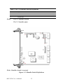
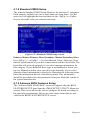
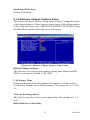
MIC-3358
6U
CompactPCI
Intel®
Pentium®
4 Processor - M
Single Board Computer with
VGA / Dual Giga LAN / PMC
User’s Manual
Copyright Notice
This document is copyrighted, 2004. All rights are reserved. The original
manufacturer reserves the right to make improvements to the products
described in this manual at any time without notice. No part of this manual may be reproduced, copied, translated or transmitted in any form or
by any means without the prior written permission of the original manufacturer. Information provided in this manual is intended to be accurate
and reliable. However, the original manufacturer assumes no responsibility for its use, nor for any infringements upon the rights of third parties
which may result from its use.
Acknowledgements
Award is a trademark of Award Software International, Inc.
IBM, PS/2, OS/2, and VGA are trademarks of International Business
Machines Corporation.
Intel® and Pentium® are trademarks of Intel Corporation.
Windows is a registered trademark of Microsoft Corporation.
NetWare is a trademark of Novell, Inc.
PICMG™, CompactPCI™ and the PICMG™, and CompactPCI™ logos
are trademarks of the PCI Industrial Computers Manufacturers Group.
All other product names or trademarks are properties of their respective
owners.
Technical Support and Sales Assistance
If you have any technical questions about the MIC-3358 or any other
Advantech products, please visit our support website at:
http://support.advantech.com.tw
For more information about Advantech's products and sales information,
please visit:
http://www.advantech.com.
Part No.2002335800
2nd Edition
Printed in Taiwan
MIC-3358 User’s Manual
December 2004
ii
CE Notification
The MIC-3358, developed by Advantech CO., LTD., has passed the CE
test for environment specification when shielded cables are used for
external wiring. We recommend the use of shielded cables.
FCC
This device complies with the requirements in part 15 of the FCC rule.
Operation is subject to the following two conditions:
(1) This device must not cause harmful interference.
(2) This device must accept any interference received, including interference that may cause undesired operation.
Product warranty
Advantech warrants to you, the original purchaser, that each of its products will be free from defects in materials and workmanship for one year
from the date of purchase. This warranty does not apply to any products
which have been repaired or altered by persons other than repair personnel authorized by Advantech, or which have been subject to misuse,
abuse, accident or improper installation. Advantech assumes no liability
under the terms of this warranty as a consequence of such events.
Because of Advantech's high quality-control standards and rigorous testing, most of our customers never need to use our repair service. If an
Advantech product is defective, it will be repaired or replaced at no
charge during the warranty period. For out-of-warranty repairs, you will
be billed according to the cost of replacement materials, service time and
freight. Please consult your dealer for more details.
If you think you have a defective product, follow these steps:
1. Collect all the information about the problem encountered. (For example, CPU speed, Advantech products used, other hardware and software
used, etc.) Note anything abnormal and list any on-screen messages you
get when the problem occurs.
2. Call your dealer and describe the problem. Please have your manual,
product, and any helpful information readily available.
3. If your product is diagnosed as defective, obtain an RMA (return merchandize authorization) number from your dealer. This allows us to process your return more quickly.
4. Carefully pack the defective product, a fully-completed Repair and
Replacement Order Card and a photocopy proof of purchase date (such as
your sales receipt) in a shippable container. A product returned without
proof of the purchase date is not eligible for warranty service.
iii
5. Write the RMA number visibly on the outside of the package and ship
it prepaid to your dealer.
Packing List
Before installing your board, ensure that the following materials have
been received:
• 1 MIC-3358 all-in-one single board computer
• 1 Utility CD-ROM disc
• 1 CPU Heat sink (Assembled)
• 1 Thermal pad (Assembled)
• 1 RJ-45 to RS-232 COM port adaptor
• 1 Hard drive isolation pad (Assembled)
• 1 Hard drive bracket (Assembled)
• 1 Solder-side cover (Assembled)
• Several screws
• 1 warranty certificate document
If any of these items are missing or damaged, contact your distributor or
sales representative immediately.
Warning!
Caution!
Any changes or modifications made to the
equipment which are not expressly approved by
the relevant standards authority could void your
authority to operate the equipment.
Danger of explosion if battery is incorrectly
installed. The battery should not be charged.
Replace only with Advantech-specified batteries.
MIC-3358 User’s Manual
iv
Contents
Chapter
1 Hardware Configuration .................................2
1.1
1.2
1.3
Introduction ....................................................................... 2
Specifications .................................................................... 3
Functional Block Diagram ................................................ 6
1.4
Jumpers.............................................................................. 6
Figure 1.1:MIC-3358 functional block diagram............. 6
1.4.1
1.4.2
1.5
Jumper Locations............................................................ 6
Table 1.1:MIC-3358 jumper descriptions....................... 6
Table 1.2:JP1 jumper definition...................................... 7
Table 1.3:JP2 jumper definitions .................................... 7
Table 1.4:JP7 jumper definitions .................................... 7
Clear CMOS (JP4) .......................................................... 7
Table 1.5:Clear CMOS JP4 ............................................ 8
Connectors......................................................................... 8
Table 1.6:MIC-3358 connector descriptions .................. 8
Table 1.7:CN1 IDE Connector Definitions .................... 9
Table 1.8:CN2 CompactFlash™ Socket Definitions.... 10
Table 1.9:CN3 RJ-45 COM1 port Definitions.............. 11
Table 1.10:CN4 Handle Switch Definitions ................. 12
Figure 1.2:Handle Switch Definitions .......................... 12
Table 1.11:CN5 USB 1.1/2.0 port Definitions ............. 13
Table 1.12:CN6 USB 1.1/2.0 port Definitions ............. 13
Table 1.13:CN9 DB-15 VGA Connector Definitions .. 14
Table 1.14:PU1 Gigabit LAN Connector Definitions .. 14
Table 1.15:J11/J12/J14 PMC Connector Definitions .. 15
Table 1.16:D9 LED Definitions.................................... 18
Table 1.17:SW1 Vcore selection definitions ................ 18
Table 1.18:SW2 Drone mode definitions ..................... 20
Figure 1.3:MIC-3358 jumpers and connectors ............. 21
Figure 1.4:MIC-3358 front panel connectors ............... 22
1.6
1.7
Safety Precautions ........................................................... 22
Installing CPU and Heat Sink ........................................ 23
1.8
Software support ............................................................. 24
Figure 1.5:Complete assembly ..................................... 24
Chapter
2 Connecting Peripherals .................................26
2.1
2.2
2.3
2.4
IDE Device (CN1 and Rear I/O) ..................................... 26
VGA Display Connector (CN9 or Rear I/O)................... 26
PS/2 Keyboard and Mouse Connector (Rear I/O)........... 26
Serial Ports (CN3 and Rear I/O) ..................................... 27
Table 2.1:MIC-3358 serial port default settings........... 27
v
2.5
2.6
2.7
2.8
2.9
Chapter
Ethernet Configuration (PU1 , Rear I/O and J3)............. 27
USB Connector (CN5/6 and Rear I/O) ........................... 28
PMC Connector (J11, J12, J14) ...................................... 28
CompactFlash™ Socket (CN2)....................................... 28
Card Installation .............................................................. 28
3 Driver Setup....................................................32
3.1
3.2
3.3
Overview ......................................................................... 32
USB driver....................................................................... 32
CMM (Chassis Management Module) Driver ................ 33
3.3.1
3.3.2
Chapter
Windows 2K Driver...................................................... 33
Figure 3.1:Select: My Computer --> Properties ........... 33
Figure 3.2:Select: Hardware --> Hardware Wizard...... 33
Figure 3.3:Select: Next ................................................. 34
Figure 3.4:Select: Add/Troubleshoot a device ............. 34
Figure 3.5:Select: Add a new device ............................ 35
Figure 3.6:Select: No .................................................... 35
Figure 3.7:Select: Other devices................................... 36
Figure 3.8:Click: Have Disk ......................................... 36
Figure 3.9:Browse for driver on CD-ROM .................. 37
Figure 3.10:Click: OK .................................................. 37
Figure 3.11:Click: OK .................................................. 38
Figure 3.12:Click: Yes.................................................. 38
Figure 3.13:Click: Next ................................................ 39
Figure 3.14:Click: Finish .............................................. 39
Figure 3.15:Click: Yes.................................................. 40
Figure 3.16:In Device Manager, select A-IPM Drivers 40
Windows XP Driver...................................................... 41
Figure 3.17:My Computer --> Properties".................... 41
Figure 3.18:Hardware --> Add Hardware Wizard........ 41
Figure 3.19:Click: Next ................................................ 42
Figure 3.20:Click: Yes.................................................. 42
Figure 3.21:Select: Add a new hardware device .......... 43
Figure 3.22:Click: Install the hardware... ..................... 43
Figure 3.23:Select: Show all devices............................ 44
Figure 3.24:Select: Have Disk ...................................... 44
Figure 3.25:Select driver on CD-ROM......................... 45
Figure 3.26:Select A-IPM driver and click: Have Disk 45
Figure 3.27:Click: Next ................................................ 46
Figure 3.28:Click: Finish .............................................. 46
Figure 3.29:My computer: A-IPM drivers.................... 47
4 Award BIOS Setup.........................................50
4.1
AWARD BIOS Setup...................................................... 50
4.1.1
MIC-3369 User’s Manual
Figure 4.1:Setup program initial screen........................ 50
Entering Setup............................................................... 50
vi
4.1.2
Standard CMOS Setup.................................................. 51
Figure 4.2:Standard CMOS setup screen...................... 51
4.1.3 Advance BIOS Features Setup ..................................... 51
Figure 4.3:Advance BIOS features setup screen .......... 52
4.1.4 Advance Chipset Features Setup .................................. 55
Figure 4.4:Advance Chipset features setup screen ....... 55
4.1.5 Integrated Peripherals ................................................... 57
Figure 4.5:Integrated Peripherals setup screen ............. 57
4.1.6 Power Management Setup ............................................ 60
Figure 4.6:Power management setup screen................. 60
4.1.7 PNP/PCI Configuration Setup ...................................... 61
Figure 4.7:PNP/PCI configuration screen .................... 61
4.1.8 PC Health Status ........................................................... 62
Figure 4.8:PC Health setup screen................................ 62
4.1.9 Load Optimized Defaults.............................................. 62
4.1.10 Set Password ................................................................. 63
4.1.11 Save & Exit Setup......................................................... 63
4.1.12 Exit Without Saving...................................................... 63
Appendix A Watchdog Timer.............................................66
A.1
Programming the Watchdog Timer................................. 66
Appendix B Pin Assignments .............................................70
B.1
J1 Connector.................................................................... 70
B.2
J2 Connector.................................................................... 71
B.3
J3 Connector.................................................................... 72
B.4
J5 Connector.................................................................... 73
B.5
System I/O Ports.............................................................. 74
B.6
Interrupt Assignments ..................................................... 75
B.7
1st MB Memory Map...................................................... 75
Table B.1:J1 connector ................................................. 70
Table B.2:J2 connector ................................................. 71
Table B.3:J3 connector ................................................. 72
Table B.4:J5 connector ................................................. 73
Table B.5:System I/O ports .......................................... 74
Table B.6:Interrupt assignments ................................... 75
Table B.7:1st MB memory map ................................... 75
vii
MIC-3369 User’s Manual
viii
CHAPTER
Hardware
Configuration
1
Chapter 1 Hardware Configuration
1.1 Introduction
The MIC-3358 is a CompactPCI® server blade with Intel® Pentium® 4
Processor-M on board to compliant with Compact Packet Switching
Backplane (cPSB) systems. Supporting the PICMG 2.16 specification,
the MIC-3358 delivers a cost performance platform for those applications
that demand high performance. It is an ideal platform for emerging application such as switch-fabric blade server, mission critical and computing
intensive applications.
The new MIC-3358 has been optimized for the Intel® Pentium® 4 Processor-M and Intel® 845E Chipset. It unveils as a high performance
cPCI platforms, delivering compelling system bus speed performance
across the 400 MHz with Intel NetBurst™ Micro-Architecture, Its innovated wider data paths and flexible memory refresh technology optimize
the DDR SDRAM performance in MIC-3358.
High Performance Intel® Pentium® 4 Processor -M
The MIC-3358 supports Intel® Pentium® 4 processor-M 1.7GHz and
2.2GHz , with u-FCPGA package. The Intel® Pentium®4 processor-M
has on-chip 512KB L2 cache providing high performance. With the support of a 400MHz front side bus, the MIC-3358 can fulfill customer’s
expectations of price-performance computing capability.
Compact Mechanical Design
The MIC-3358 has many functions on a single board with only one-slot
width. Advantech provides a CPU heat sink specially designed for the
Intel® Pentium®4 processor -M, enabling the MIC-3358 to operate without a cooling fan on the heat sink. It only needs external cooling air from
the chassis fans for ventilation. This enables the MIC-3358 to use Intel®
Pentium®4 processor - M within a mere 1-slot wide space.
Single P2P Bridge
The MIC-3358 with single PCI-to-PCI Bridge is applicable up to 8-slot
enclosure and drive up to seven bus master PCI slots in master mode. Furthermore, it supports master and drone modes. The MIC-3358 can also
operate in drone mode in a peripheral slot, whereby it functions as a
stand-alone computer and does not communicate on the CompactPCI®
bus.
MIC-3358 User’s Manual
2
PMC (PCI Mezzanine Card) IEEE1386.1 Compliant
The MIC-3358 support one PMC site and compliant with PICMG 2.3
(PCI Mezzanine Card) specification. This 32-bit/33MHz PMC interface
provides front access capability by PMC modules for various function
demanding.
Complete I/O Functions
The MIC-3358 offers all the I/O functions of an industrial computer with
the rugged Eurocard form factor. The rest of I/O have fully connected to
the rear I/O module via user-define connector (J3 and J5) on the backplane. These I/O contain one Gigabit Ethernet port, one RJ-45 COM port,
two USB 2.0 ports, one VGA connector, and one PMC site. The front
panel also has a reset button and LEDs for hot swap indication, power status, HDD operation and Ethernet communication. The built-in high speed
IDE controller provides two separate IDE channels with Ultra DMA/33/
66/100 mode. The user-defined J3 connector is designed to support two
IDE devices, one floppy drives, one printer device, LAN 1/2 for PCIMG
2.16. These drives can simply be connected to the backplane or to the rear
transition board for easy service and maintenance.
Meets Switch Fabric, Mission Critical and Computing Intensive
Application requirements
Supporting the PICMG 2.16 specification, the MIC-3358 delivers a cost
performance platform for those applications that demand for low power
and high performance. It is an ideal platform for emerging application
such as switch-fabric blade server, mission critical and computing intensive applications like third-generation (3G) wireless, voice over Internet
protocol (VoIP), networking, image processing and the converged data
and voice communication applications.
The two-layer front panel design complies with IEEE 1101.10. Connectors are firmly screwed to the front panel, and the replaceable shielding
gasket is attached to the panel edge. This reduces emissions and gives
better protection against external interference. A watchdog timer can
automatically reset the system if the system stops abnormally.
1.2 Specifications
Standard SBC Functions
• CPU: Intel® Pentium® 4 processor-M u-FCPGA socket
• BIOS: Award 4Mb flash memory
3
Chapter 1
• Chipset: Intel® 845E/ICH4 Chipset
• Front Side Bus: 400MHz (Intel® Pentium® 4 processor-M Processor)
• Bus Interface: PCI 32-bit/33 MHz
• 2nd level cache: Built-in 512KB on Intel® Pentium® 4 processor-M
die
• RAM: 512MB ECC DDR266 memory on board. Support up to 2GB
ECC DDR200/266.
• Enhanced IDE interface: Two channels handles one 2.5” IDE in SBC
and two IDEs in RIO module via J3 connector. Supports PIO mode 4
and ATA 33/66/100 mode. One IDE connector and space reserved for
embedded 2.5” HDD.
• Serial ports: One RJ-45 COM1 port (RS-232 interface) with 16C550
compatible UARTs
• USB port: Two USB ports with fuse protection comply with USB
specification 2.0/1.1
• CompactFlash socket: one CompactFlash socket on board.
• PMC expansion slot: One 32bit/33MHz PCI Mezzanine site on board
with +5V/+3.3V compliant.
• Watchdog timer: It provides system reset, interrupt and NMI support
via software control. Time interval is from 1 to 255 seconds.
PCI-to-PCI Bridge
• Controller chip: One PCI-to-PCI bridge controller chip provides master and drone mode
• (Master mode) Supports up to seven bus masters peripherals on each
bus segment
• (Drone mode) it could plug into a peripheral slot as a “drone mode” ,
whereby it functions as stand-alone computer.
10/100/1000Base-TX Ethernet Interface
• Controller chips: Two Intel® 82540EM Gigabit Ethernet controller
chips provides Dual Gigabit ports
• One front RJ-45 Gigabit LAN port
• 10 Mbps, 100 Mbps and 1000Mbps auto-switching
PCI VGA Interface
• Controller: ATI Rage XL
• PCI 2.2 compliant, 32bit/33 MHz
MIC-3358 User’s Manual
4
• Display memory: 8MB SDRAM VRAM
• Display Resolution Number of Colors:
:
2D Display Modes: Resolutions, Colors and Maximum Refresh Rates (Hz)
Resolution
640x 480
800x 600
1024x 768
1152x 864
1280x 1024
1600x 1200
256 colors
200
200
150
120
100
85
65K colors
200
200
150
120
100
85
16.7M colors
200
200
150
120
100
75
Maximum 3D Resolution(Hz)
8MB
65K colors
1600x1200
16.7M colors
1280x1024
Optional Rear I/O Boards
• RIO-3309
NOTE:
MIC-3358 does not support MIC-3960 storage
carrier board
Mechanical and Environmental Specifications
• Operating temperature: 0 ~ 55° C (32 ~ 131° F)
• Storage Temperature: -20 ~ 80° C (-4 ~ 176° F)
• Humidity (Non-operating): 5~95%@60° C (non-condensing)
• Max Power Consumption: +5V / 4.19A, +3.3V / 4.5A, +12V / 35mA
• Board size: 233.35 x 160 mm (6U size), 1-slot (4 TE) wide
• Weight: 0.8 kg (1.76 lb)
• Shock: 20 G (operating); 50 G (Non-operating)
• Random vibration: 1.5 Grms (operating), 2.0 Grms (Non-Operating)
5
Chapter 1
1.3 Functional Block Diagram
32
33
33
Figure 1.1: MIC-3358 functional block diagram.
Note: MIC-3358 does not support shutdown function of ATX power supply.
1.4 Jumpers
1.4.1 Jumper Locations
Table 1-1 lists the jumper function. Figure 1-1 illustrates the jumper location. Read this section carefully before changing the jump setting on your
MIC-3358 card.
Table 1.1: MIC-3358 jumper descriptions
JP1
PMC module voltage V(i/o)
JP2
VGA output selector
JP4
Clear CMOS
JP7
CompactFlash™ card mode setting
MIC-3358 User’s Manual
6
Table 1.2: JP1 jumper definition
5V
3.3V (Default)
Table 1.3: JP2 jumper definitions
VGA output in Rear IO
VGA output in front panel of MIC-3358
Table 1.4: JP7 jumper definitions
Master
Slave (default)
1.4.2 Clear CMOS (JP4)
This jumper is used to erase CMOS data and reset system BIOS information. Follow the procedures below to clear the CMOS.
1. Turn off the system.
2. Close jumper JP4 (1-2) for about 3 seconds.
3. Set jumper JP4 (2-3) as normal.
4. Turn on the system. The BIOS is reset to its default setting.
7
Chapter 1
Table 1.5: Clear CMOS JP4
Clear
Normal (default)
1.5 Connectors
On-board connectors link to external devices such as hard disk drives,
keyboards, or floppy drives, etc. Table 1-6 lists the function of each connector and Figure 1-1 and Figure 1-2 illustrate each connector location.
Chapter 2 gives instructions for connecting external devices to your card.
Table 1.6: MIC-3358 connector descriptions
Number
Function
CN1
2.5" IDE Connector
CN2
CompactFlash™ Socket
CN3
RJ-45 COM1 port
CN4
Handle Switch
CN5
USB 1.1/2.0 port
CN6
USB 1.1/2.0 port
CN8
Reset Switch
CN9
DB-15 VGA Connector
PU1
Gigabit RJ-45 LAN Connector
J11/J12/J14
PMC Connector
J1/J2
Primary CompactPCI™ bus
J3/J5
Rear I/O transition
D9
HDD LED and Power LED
LED1
Hot Swap LED
SW1
Vcore selection
SW2
Drone mode Selection
MIC-3358 User’s Manual
8
Table 1.7: CN1 IDE Connector Definitions
Pin
Signal
Pin
Signal
1
PRST#
2
GND
3
PID7
4
PID8
5
PID6
6
PID9
7
PID5
8
PID10
9
PID4
10
PID11
11
PID3
12
PID12
13
PID2
14
PID13
15
PID1
16
PID14
17
PID0
18
PID15
19
GND
20
N/C
21
PDRQ#
22
GND
23
PIOW#
24
GND
25
PIOR#
26
GND
27
PRDY
28
CSEL*
29
PACK#
30
GND
31
PIRQ
32
N/C
33
PDA1
34
PDIAG#**
35
PDA0
36
PDA2
37
PCS1#
38
PCS3#
39
HDD_LED
40
N/C
41
+5V
42
+5V
43
GND
44
N/C
#: active low
*: CSEL connected to GND
**: PDIAG# has 10K ohm pull-down to GND
9
Chapter 1
Table 1.8: CN2 CompactFlash™ Socket Definitions
Pin
Signal
Pin
Signal
1
GND
26
N/C
2
ID3
27
ID11
3
ID4
28
ID12
4
ID5
29
ID13
5
ID6
30
ID14
6
ID7
31
ID15
7
HCS1-
32
HCS3-
8
GND
33
N/C
9
GND
34
HIOR-
10
GND
35
HIOW-
11
GND
36
N/C
12
GND
37
HIRQ
13
+5V
38
+5V
14
GND
39
SANDISK
15
GND
40
N/C
16
GND
41
-HRST1
17
GND
42
HRDY
18
GDA2
43
N/C
19
HDA1
44
N/C
20
HDA0
45
SANLED
21
ID0
46
N/C
22
ID1
47
ID8
23
ID2
48
ID9
24
N/C
49
ID10
25
N/C
50
GND
MIC-3358 User’s Manual
10
Table 1.9: CN3 RJ-45 COM1 port Definitions
Pin
Signal
1
NRLSD1
2
NRX1
3
NTX1
4
NDTR1
5
GND
6
NDSR1
7
NRTS1
8
NCTS1
11
Chapter 1
Table 1.10: CN4 Handle Switch Definitions
Pin
Signal
1
common
2
normal closed
3
normal open
Note:
Pin 1-2 handle closed
Pin 1-3 handle open
Note: Handle closed is normal
Figure 1.2: Handle Switch Definitions
MIC-3358 User’s Manual
12
Table 1.11: CN5 USB 1.1/2.0 port Definitions
Pin
Signal
1
+5V
2
USB_P2-
3
USB_P2+
4
GND
Table 1.12: CN6 USB 1.1/2.0 port Definitions
Pin
Signal
1
+5V
2
USB_P2-
3
USB_P2+
4
GND
13
Chapter 1
Table 1.13: CN9 DB-15 VGA Connector Definitions
Pin
Signal
1
RED
2
GREEN
3
BLUE
4
N/C
5
GND
6
GND
7
GND
8
GND
9
N/C (VGAVCC)
10
GND
11
N/C
12
VGA_SDA
13
HSYNC
14
VSYNC
15
VGA_SCL
Table 1.14: PU1 Gigabit LAN Connector Definitions
Pin
Signal
1
MDIAX1+
2
MDIAX1-
MIC-3358 User’s Manual
14
3
MDIAX2+
4
MDIAX3+
5
MDIAX3-
6
MDIAX2-
7
MDIAX4+
8
MDIAX4-
The LED indicator means
Left
Right
10Mbps
Off
flick active/link mode
100Mbps
Green
1000Mbps
Orange
Table 1.15: J11/J12/J14 PMC Connector Definitions
J11 PIN SIGNAL
PIN#
Single Name
PIN#
Single Name
1
TCK
2
-12V
3
GND
4
INTC#
5
INTD#
6
INTA#
7
BUSMODE1
8
+5V
9
INTB#
10
N/C
11
GND
12
N/C
13
CLK
14
GND
15
GND
16
GNT4#
17
REQ4#
18
+5V
19
V(I/O)
20
AD31
21
AD28
22
AD27
23
AD25
24
GND
25
GND
26
C/BE3#
27
AD22
28
AD21
29
AD19
30
+5V
31
V(I/O)
32
AD17
15
Chapter 1
33
FRAME#
34
GND
35
GND
36
IRDY#
37
DEVSEL#
38
+5V
39
GND
40
LOCK#
41
SDONE#
42
SBO#
43
PAR
44
GND
45
V(I/O)
46
AD15
47
AD12
48
AD11
49
AD9
50
+5V
51
GND
52
C/BE0#
53
AD6
54
AD5
55
AD4
56
GND
57
V(I/O)
58
AD3
59
AD2
60
AD1
61
AD0
62
+5V
63
GND
64
REQ64#
J12 PIN SIGNAL
PIN#
Single Name
PIN#
Single Name
1
+12V
2
TRST#
3
TMS
4
TDO
5
TDI
6
GND
7
GND
8
N/C
9
N/C
10
N/C
11
BUSMODE2#
12
+3.3V
13
RST#
14
BUSMODE3#
15
+3.3V
16
BUSMODE4#
17
N/C
18
GND
19
AD30
20
AD29
21
GND
22
AD26
23
AD24
24
+3.3V
25
IDSEL(AD19)
26
AD23
27
+3.3V
28
AD20
29
AD18
30
GND
31
AD16
32
C/BE2#
33
GND
34
N/C
35
TRDY#
36
+3.3V
37
GND
38
STOP#
39
PERR#
40
GND
MIC-3358 User’s Manual
16
41
+3.3V
42
43
C/BE1#
44
SERR#
GND
45
AD14
46
AD13
47
GND
48
AD10
49
AD8
50
+3.3V
51
AD7
52
N/C
53
+3.3V
54
N/C
55
N/C
56
GND
57
N/C
58
N/C
59
GND
60
N/C
61
ACK64#
62
+3.3V
63
GND
64
N/C
J14 Pin Signal
PIN#
Single Name
PIN#
Single Name
1
+5Vaux
2
+5V
3
+5Vaux
4
+5V
5
GND
6
GND
7
N/C
8
N/C
9
N/C
10
N/C
11
N/C
12
N/C
13
N/C
14
N/C
15
N/C
16
N/C
17
N/C
18
N/C
19
N/C
20
N/C
21
N/C
22
N/C
23
N/C
24
N/C
25
N/C
26
N/C
27
BMC_PWR_ON/OFF
28
N/C
29
BMC_PWROK
30
PMC_OS_SHUTDOWN
31
GA1
32
GA0
33
GA3
34
GA2
35
N/C
36
GA4
37
N/C
38
BMC_BD_SEL#
39
N/C
40
N/C
41
N/C
42
N/C
43
N/C
44
N/C
45
N/C
46
N/C
17
Chapter 1
47
CMM1_SCL
48
49
CMM2_SCL
50
CMM1_SDA
CMM2_SDA
51
BMC_BD_SEL
52
N/C
53
N/C
54
N/C
55
BMC_LEDA
56
BMC_LEDL
57
GND
58
GND
59
BMC_TX+
60
BMC_RX+
61
BMC_TX-
62
BMC_RX-
63
GND
64
GND
Table 1.16: D9 LED Definitions
Green
Power Status
Yellow
HDD Status
Table 1.17: SW1 Vcore selection definitions
MIC-3358 User’s Manual
18
It's automatic selection when SW1-1~SW1-6 are all OFF.
SW1- 6
SW1- 5 SW1- 4 SW1- 3
SW1- 2
SW1- 1
VCORE
OFF
X
X
X
X
X
AUTO
ON
ON
ON
ON
ON
ON
1.750V
ON
ON
ON
ON
ON
OFF
1.700V
ON
ON
ON
ON
OFF
ON
1.650V
ON
ON
ON
ON
OFF
OFF
1.600V
ON
ON
ON
OFF
ON
ON
1.550V
ON
ON
ON
OFF
ON
OFF
1.500V
ON
ON
ON
OFF
OFF
ON
1.450V
ON
ON
ON
OFF
OFF
OFF
1.400V
ON
ON
OFF
ON
ON
ON
1.350V
ON
ON
OFF
ON
ON
OFF
1.300V
ON
ON
OFF
ON
OFF
ON
1.250V
ON
ON
OFF
ON
OFF
OFF
1.200V
ON
ON
OFF
OFF
ON
ON
1.150V
ON
ON
OFF
OFF
ON
OFF
1.100V
ON
ON
OFF
OFF
OFF
ON
1.050V
ON
ON
OFF
OFF
OFF
OFF
1.000V
ON
OFF
ON
ON
ON
ON
0.975V
ON
OFF
ON
ON
ON
OFF
0.950V
ON
OFF
ON
ON
OFF
ON
0.925V
ON
OFF
ON
ON
OFF
OFF
0.900V
PS: X means either ON or OFF.
19
Chapter 1
Table 1.18: SW2 Drone mode definitions
SW2
ON
1
2
When SW2 is ON, then the board is selected as drone mode. The rest of
the combination is reserved for other modes.
Please refer to Appendix B for J1/2/3/5 pin assignments.
MIC-3358 User’s Manual
20
Figure 1.3: MIC-3358 jumpers and connectors
21
Chapter 1
Figure 1.4: MIC-3358 front panel connectors
1.6 Safety Precautions
Follow these simple precautions to protect yourself from harm and the
products from damage.
1. To avoid electric shock, always disconnect the power from your PC
chassis before you work on it. Don't touch any components on the CPU
card or other cards while the PC is on.
MIC-3358 User’s Manual
22
2. Disconnect power before making any configuration changes. The sudden rush of power as you connect a jumper or install a card may damage
sensitive electronic components.
3. Always ground yourself to remove any static charge before you touch
your CPU card. Be particularly careful not to touch the chip connectors.
Modern integrated electronic devices, especially CPUs and memory
chips, are extremely sensitive to static electric discharges and fields. Keep
the card in its antistatic packaging when it is not installed in the PC, and
place it on a static dissipative mat when you are working with it. Wear a
grounding wrist strap for continuous protection.
1.7 Installing CPU and Heat Sink
The MIC-3358 supports Intel® Pentium® 4 processor - M . In order to
meet critical environmental conditions and the physical space of the
MIC-3358 at the same time, Advantech designed a heat sink to fulfill its
primary needs. Please refer to Figure 1-4 for an illustration of the heat
sink used for the MIC-3358.
The small aluminum plate is default fastened on the CPU in the factory.
When user doing the memory installation, the following steps should be
followed:
1.
Remove the screws for the solder side cover. At this step, the front
panel will be also loose. Be careful about any improper disassemble procedure that could cause any damage of SBC.
2.
Remove the rest four screws for heatsink standing, then the heatsink is loose for memory installation and relavant.
3.
Follow the opposed procedure to assembly the heatsink and solder
side cover.
Note:
The heat pad is sealed between heatsink and
CPU is kind of frangible, please be careful on the
disassemble procedure. And be careful with any
other damage of heat pad will cause the thermal
issue easily.
23
Chapter 1
Figure 1.5: Complete assembly
1.8 Software support
The MIC-3358 comes with a utility CD-ROM disc, which includes drivers and utility programs of Gigabit Ethernet, IAA and VGA interfaces.
The drivers support Windows 2000, XP and NT4.0 Operation systems.
Please visit Intel® website for detailed explanation.
MIC-3358 User’s Manual
24
CHAPTER
2
Connecting
Peripherals
Chapter 2 Connecting Peripherals
2.1 IDE Device (CN1 and Rear I/O)
The MIC-3358 provides two IDE (Integrated Device Electronics) channels via CN1 connector in MIC-3358 or via the J3 connector to the rear
transition board (RIO-3309C). CN1 connector support one 2.5" IDE
HDD in MIC-3358 and two IDE drives can be connected to Secondary
IDE connector (CN19) in the rear transition board. If two drives are
installed on one channel, remember to set one as the master and the other
one as the slave. You may do this by setting the jumpers on the drives.
Refer to the documentation that came with your drive for more information. A jumper diagram usually appears on the topside of a hard disk
drive.
Warning: Plug the other end of the cable into the drive with pin #1 on the
cable corresponding to pin #1 on the drive. Improper connection will
damage the drive.
2.2 VGA Display Connector (CN9 or Rear I/O)
The MIC-3358 provides a VGA chipset (ATI Rage XL) built-in display
for high performance application. The CN9 connector of MIC-3358 and
CN7 connector of rear I/O board are both DB-15 connector for VGA
monitor input. The system monitor display is able to be selected by
jumper JP2.
2.3 PS/2 Keyboard and Mouse Connector (Rear I/O)
The MIC-3358 provides Keyboard/Mouse support via J5 connector to the
rear transition board which builds in one PS/2 Keyboard/Mouse connector (CN12). The package - one Y-type PS/2 keyboard/mouse cable - provides two transferred connectors. Since these two connectors are
identical, please, follow the icons on the cable to plug the keyboard and
the mouse into their correct connectors.
MIC-3358 User’s Manual
26
2.4 Serial Ports (CN3 and Rear I/O)
The MIC-3358 offers one serial ports: COM1 in RS-232. With limited
front panel access, one COM1 (CN3) can be connected via a RJ-45 to RS232 adaptor and COM2 (CN9) interface has to be connected via rear I/O
module (RIO-3309C) for implement. These ports allow users to connect
to serial devices (a mouse, printers, etc.) or a communication network.
You can select the address for each port to disable it, using the BIOS
Advanced Setup program, covered in Chapter 5. Different devices implement the RS-232 standard in different ways. If you are having problems
with a serial device, be sure to check the pin assignments for the connector. The IRQ and address range for both ports are fixed. However, if you
wish to disable the port or change these parameters later, you can do this
in the system BIOS setup. The table below shows the settings for the
MIC-3358 board's ports:
Table 2.1: MIC-3358 serial port default settings
Port
COM1
COM2
Address
3F8, 3E8
2F8, 2E8
Default
IRQ4
IRQ3
2.5 Ethernet Configuration (PU1 , Rear I/O and J3)
The MIC-3358 is equipped with dual high performance 32-bit PCI-bus
Gigabit Ethernet interfaces which are fully compliant with IEEE 802.3u
10/100/1000Base-TX specifications. Users can select front GbE or rear
GbE or 2.16 by BIOS. Users can choice LAN1 connector either via front
RJ-45 jack (PU1) in MIC-3358 or rear RJ-45 (CN16) in rear module.
Another one Gigabit LAN connector (CN15) has to go through RIO module (RIO-3309C).
Moreover, the MIC-3358 supports PICMG 2.16 complaint with Packet
Switching Backplane Specification via J3 connector, it will installed in
PICMG 2.16 backplane as switch-fabric applications blade server
27
Chapter 2
2.6 USB Connector (CN5/6 and Rear I/O)
The MIC-3358 provides two USB (Universal Serial Bus) 2.0 channels
either via two front USB ports (CN5 and CN6) in MIC-3358 or via J5
connector to one USB connector (CN8) in real transition board. The USB
interface gives complete plug and play, hot attach/detach for up to 127
external devices. The MIC-3358 USB interface complies with USB specification rev. 2.0 and is polyswitch protected. The USB interface can be
disabled in the system BIOS setup. The USB controller default is
"Enabled" but the USB keyboard support default is "Disabled".
2.7 PMC Connector (J11, J12, J14)
The MIC-3358 supports one PMC (PMC Mezzanine Card) modules on
PCI bus. This 32-bit, 3.3/5 V(I/O) PCI bus is available at connectors J11
and J12. J14 is applied for user definitions. Front panel access is provided
for the PMC interface.
2.8 CompactFlash™ Socket (CN2)
CompactFlash™ is a standard form factor for mass storage and I/O cards.
Based on the PCMCIA Standard, CompactFlash™ cards are approximately 1/4 the volume of a PC Card. In order to achieve the small size,
the interface pin count is 50-pins compared to the PCMCIA's 68-pin.
The MIC-3358 supports one CompactFlash™ socket in CN2 connector. It
helps file and data storage in the CompactFlash™ card rather than the traditional hard drive.
2.9 Card Installation
The CompactPCI™ connectors are firm and rigid, and require careful
handling while plugging and unplugging. Improper installation of a card
can easily damage the backplane of the chassis. The inject/eject handles
MIC-3358 User’s Manual
28
of MIC-3358 help you install and remove the card easily and safely. Follow the procedure below to install the
MIC-3358 into a chassis:
To install a card:
1. Hold the card vertically. Be sure that the card is pointing in the correct
direction. The components of the card should be pointing to the righthand side.
2. Pull out both handles to unlock it.
Caution: Keep your fingers away from the hinge to prevent your
fingers from getting pinched.
3. Insert the card into the chassis by sliding the upper and lower edges of
the card into the card guides.
4. Push the card into the slot gently by sliding the card along the card
guide until the handles meet the rectangular holes of the cross rails. Note:
If the card is correctly positioned and has been slid all the way into the
chassis, the handle should match the rectangular holes. If not, remove the
card from the card guide and repeat step 3 again. Do not try to install a
card by forcing it into the chassis.
5. Pull the upper handle down and lift the lower handle up to push the
card into place.
6. Secure the card by pushing in the red handle to lock it into place.
To remove a card:
1. Unscrew the screws on the front panel.
2. Lift the upper handle up and press the lower handle down to release the
card from the backplane.
3. Slide the card out.
29
Chapter 2
MIC-3358 User’s Manual
30
CHAPTER
3
Driver Setup
Chapter 3 Driver Setup
3.1 Overview
Advantech provides CD utility driver in the package. Please install
Chipset INF driver, VGA graphics driver, LAN driver and Intel® Application Accelerator (IAA) driver sequentially.
The Intel® Application Accelerator is a performance software package of
Intel® chipsets. It reduces the storage sub-system bottleneck, enabling
faster delivery of data from the hard drive to the processor and other system level hardware. Meanwhile, it enables a performance-enhancing data
pre-fetcher for Intel® Pentium® 4 and Pentium® M processor-based systems. In addition, it delivers faster overall system boot times by significantly accelerating the load time of the OS - enabling you to build
Pentium® 4 and Pentium® M processor-based systems with a better
overall end-user experience. IAA supports 48-bit Logical Block Addressing (48-bit LBA) for 137 GB and larger hard drives. Furthermore, IAA
enables Automatic Selection of Highest DMA Transfer Mode by the
ATA/ATAPI device/Intel chipset.
3.2 USB driver
If the manufacturer/vendor of a USB device recommends downloading
an Intel® USB driver update as part of troubleshooting your USB device,
please contact Microsoft® for USB driver support. Intel manufactures the
host controller but the driver is from Microsoft. While users installed
Intel INF driver, it will not install USB driver. Please go to "device manager" to update USB driver via Advantech CD utility or via Microsoft
website.
Note:
There are no separate USB (version 1.1 and
earlier) drivers available for download for Intel®
chipsets.
MIC-3358 User’s Manual
32
3.3 CMM (Chassis Management Module) Driver
MIC-3358 supports MIC-3924B CMM. Please install the driver according to the following procedure.
3.3.1 Windows 2K Driver
Figure 3.1: Select: My Computer --> Properties
Figure 3.2: Select: Hardware --> Hardware Wizard
33
Chapter 3
Figure 3.3: Select: Next
Figure 3.4: Select: Add/Troubleshoot a device
MIC-3358 User’s Manual
34
Figure 3.5: Select: Add a new device
Figure 3.6: Select: No
35
Chapter 3
Figure 3.7: Select: Other devices
Figure 3.8: Click: Have Disk
MIC-3358 User’s Manual
36
Figure 3.9: Browse for driver on CD-ROM
Figure 3.10: Click: OK
37
Chapter 3
Figure 3.11: Click: OK
Figure 3.12: Click: Yes
MIC-3358 User’s Manual
38
Figure 3.13: Click: Next
Figure 3.14: Click: Finish
39
Chapter 3
Figure 3.15: Click: Yes
Figure 3.16: In Device Manager, select A-IPM Drivers
MIC-3358 User’s Manual
40
3.3.2 Windows XP Driver
Figure 3.17: My Computer --> Properties"
Figure 3.18: Hardware --> Add Hardware Wizard
41
Chapter 3
Figure 3.19: Click: Next
Figure 3.20: Click: Yes
MIC-3358 User’s Manual
42
Figure 3.21: Select: Add a new hardware device
Figure 3.22: Click: Install the hardware...
43
Chapter 3
Figure 3.23: Select: Show all devices
Figure 3.24: Select: Have Disk
MIC-3358 User’s Manual
44
Figure 3.25: Select driver on CD-ROM
Figure 3.26: Select A-IPM driver and click: Have Disk
45
Chapter 3
Figure 3.27: Click: Next
Figure 3.28: Click: Finish
MIC-3358 User’s Manual
46
Figure 3.29: My computer: A-IPM drivers
47
Chapter 3
MIC-3358 User’s Manual
48
CHAPTER
4
Award BIOS Setup
Chapter 4 Award BIOS Setup
4.1 AWARD BIOS Setup
Once you enter Award® BIOS CMOS Setup Utility, the Main Menu (Figure 4-1) will appear on the screen. The Main Menu allows you to select
from nine setup functions and two exit choices. Use arrow keys to select
among the items and press <Enter> to accept or enter the sub-menu.
Figure 4.1: Setup program initial screen
Award's BIOS ROM has a built-in Setup program that allows users to
modify the basic system configuration. This type of information is stored
in battery-backed CMOS so that it retains the Setup information when the
power is turned off.
4.1.1 Entering Setup
Turn on the computer and check for the "patch code". If there is a number
assigned to the patch code, it means that the BIOS support your CPU. If
there is no number assigned to the patch code, please contact Advantech's
application engineer to obtain an up-to-date patch code file. This will
ensure that your CPU's system status is valid. After ensuring that you
have a number assigned to the patch code, press <DEL> and you will
immediately be allowed to enter Setup.
MIC-3358 User’s Manual
50
4.1.2 Standard CMOS Setup
The items in Standard CMOS Setup Menu are divided into 11 categories.
Each category includes no, one or more than one setup items. Use the
arrow keys to highlight the item and then use the <PgUp> or <PgDn>
keys to select the value you want in each item.
Figure 4.2: Standard CMOS setup screen.
Primary Master/Primary Slave/Secondary Master/Secondary Slave
Press PgUp/<+> or PgDn/<-> to select Manual, None, Auto type. Note
that the specifications of your drive must match with the drive table. The
hard disk will not work properly if you enter improper information for
this category. If your hard disk drive type is not matched or listed, you
can use Manual to define your own drive type manually. If you select
Manual, related information is asked to be entered to the following items.
Enter the information directly from the keyboard. This information
should be provided in the documentation from your hard disk vendor or
the system manufacturer.
4.1.3 Advance BIOS Features Setup
The "Advance BIOS FEATURES" screen will appear after the BIOS
FEATURES SETUP item from the CMOS SETUP UTILITY Menu was
chosen. This screen allows the user to configure the board according to
his particular requirements. Below are some major items that are provided in the BIOS FEATURES SETUP screen:
51
Chapter 4
Figure 4.3: Advance BIOS features setup screen
Virus Warning
During and after the system boots up, any attempt to write to the boot sector or partition table of the hard disk drive will halt the system. If this
happens, a warning message will be displayed. You can run the anti-virus
program to locate the problem. If Virus Warning is disabled, no warning
message will appear if anything attempts to access the boot sector or hard
disk partition.
CPU L1 & L2 Cache
The default value is Enabled.
Enabled (default)
Enable cache
Disabled
Disable cache
Note: The internal cache is built in the processor.
Quick Power On Self Test
This category speeds up Power On Self Test (POST) after you power on
the computer. If this is set to Enabled, BIOS will shorten or skip some
check items during POST.
Enabled (default)
Enable quick POST
Disabled
Normal POST
MIC-3358 User’s Manual
52
First/Second/Third Boot Device and Boot Other Device
The BIOS attempts to load the operating system from the devices in the
sequence selected in these items. The settings are Floppy, LS120, HDD0, SCSI, CDROM, HDD-1, HDD-2, HDD-3, ZIP100, USB-FDD, USBZIP, USB-CDROM, USB-HDD, LAN and Disabled.
Default
First boot device
Floppy
Second boot device
HDD-0
Third boot device
CD-ROM
PS: When you boot by USB CD-ROM, please install Win XP with SP1 or
Win 2000 with SP3.
Swap Floppy Drive
Switches the floppy disk drives between being designated as A and B.
Default is Disabled.
Boot Up Floppy Seek
During POST, BIOS will determine if the floppy disk drive installed is 40
or 80 tracks. 360K type is 40 tracks while 760K, 1.2M and 1.44M are all
80 tracks. Default is Enabled.
Boot Up NumLock Status
The default value is On.
On (default)
Keypad is numeric keys.
Off
Keypad is arrow keys.
Gate A20 Option
Normal
The A20 signal is controlled by keyboard controller or
chipset hardware.
Fast(default)
The A20 signal is controlled by port 92 or chipset specific method.
53
Chapter 4
Typematic Rate Setting
Key strokes repeat at a rate determined by the keyboard controller. When
enabled, the typematic rate and typematic delay can be selected. The settings are: Enabled/Disabled. Default is Disabled.
Typematic Rate (Chars/Sec)
Set the number of times a second to repeat a key stroke when you hold the
key down. The settings are: 6, 8, 10, 12, 15, 20, 24, 30.
Typematic Delay (Msec)
Sets the delay time after the key is held down before it begins to repeat
the keystroke. The settings are: 250, 500, 750, 1000.
Security Option
This category allows you to limit access to the system and Setup, or just
to Setup.
System
The system will not boot and access to Setup will be
denied if the correct password is not entered at the
prompt.
Setup(default)
The system will boot, but access to Setup will be
denied if the correct password is not entered at the
prompt.
APIC Mode (Advanced Programmable Interrupt Controller)
Default is Enabled.
MPS Version Control for OS
The options includes 1.1 and 1.4. Default is 1.4
OS Select For DRAM > 64MB
Allows OS2® to be used with > 64 MB of DRAM. Settings are Non-OS/
2 (default) and OS2. Set to OS/2 if using more than 64MB and running
OS/2®.
MIC-3358 User’s Manual
54
Small logo (EPA) show
Default is Disabled.
4.1.4 Advance Chipset Features Setup
The Advanced Chipset Features Setup option is used to change the values
of the chipset registers. These registers control most of the system options
in the computer. Choose the "ADVANCED CHIPSET FEATURES" from
the Main Menu and the following screen will appear.
Figure 4.4: Advance Chipset features setup screen
DRAM Timing Configure
This field lets you select system memory timing data. Manual and BY
SPD are two options. Default is "BY SPD"
CAS Latency Time
When synchronous DRAM is installed, the number of clock cycles of
CAS latency depends on the DRAM timing. The settings are: 1.5, 2 and
2.5.
Active to Precharge Delay
This field let you select active to precharge delay. The settings are: 7, 6
and 5
DRAM RAS# to CAS# Delay
55
Chapter 4
This field lets you insert a timing delay between the CAS and RAS strobe
signals, used when DRAM is written to, read from, or refreshed. Fast
gives faster performance; and Slow gives more stable performance. This
field applies only when synchronous DRAM is installed in the system.
The settings are: 2 and 3.
DRAM RAS# Precharge
If an insufficient number of cycles is allowed for the RAS to accumulate
its charge before DRAM refresh, the refresh may be incomplete and the
DRAM may fail to retain data. Fast gives faster performance; and Slow
gives more stable performance. This field applies only when synchronous
DRAM is installed in the system. The settings are: 2 and 3.
DRAM Data Integrity Mode
The settings are ECC (Default) and non-ECC.
Memory Frequency For
User can select 3 options: DDR200, DDR266, Auto (Default)
System BIOS Cacheable
Selecting Enabled allows caching of the system BIOS ROM at F0000hFFFFFh, resulting in better system performance. However, if any program writes to this memory area, a system error may result. The settings
are: Enabled (Default) and Disabled.
Video BIOS Cacheable
Select Enabled allows caching of the video BIOS, resulting in better system performance. However, if any program writes to this memory area, a
system error may result. The settings are: Enabled and Disabled
(Default).
Memory Hole At 15M-16M
You can reserve this area of system memory for ISA adapter ROM. When
this area is reserved, it cannot be cached. The user information of peripherals that need to use this area of system memory usually discusses their
memory requirements. The settings are: Enabled and Disabled (Default).
MIC-3358 User’s Manual
56
Delayed Transaction
The chipset has an embedded 32-bit posted write buffer to support delay
transactions cycles. Select Enabled to support compliance with PCI specification version 2.1. The settings are: Enabled (Default) and Disabled.
4.1.5 Integrated Peripherals
Figure 4.5: Integrated Peripherals setup screen
57
Chapter 4
On-Chip Primary/Secondary PCI IDE
The integrated peripheral controller contains an IDE interface with support for two IDE channels. Select Enabled to activate each channel separately. The settings are: Enabled (Default) and Disabled.
IDE Primary/Secondary Master/Slave PIO
The four IDE PIO (Programmed Input/Output) fields let you set a PIO
mode (0-4) for each of the four IDE devices that the onboard IDE interface supports. Modes 0 through 4 provide successively increased performance. In Auto mode, the system automatically determines the best mode
for each device. The settings are: Auto (Default), Mode 0, Mode 1, Mode
2, Mode 3, Mode 4.
IDE Primary/Secondary Master/Slave UDMA
Ultra DMA/33 implementation is possible only if your IDE hard drive
supports it and the operating environment includes a DMA driver (Windows 95 OSR2 or a third-party IDE bus master driver). If your hard drive
and your system software both support Ultra DMA/33 and Ultra DMA/66
and Ultra DMA/100, select Auto to enable BIOS support. The settings
are: Auto (Default), Disabled.
USB Controller
Select Enabled if your system contains a Universal Serial Bus (USB) 1.1
controller. The settings are: Enabled (Default), Disabled.
USB 2.0 Controller
Select Enabled if your system contains a Universal Serial Bus (USB) 1.1/
2.0 controller. The settings are: Enabled (Default), Disabled.
USB Keyboard/Mouse Support
Select Enabled if you use USB KB/Mouse in DOS mode.
Init Display First
User can choose display priority on either peripheral PCI slot or on board
VGA chip. There are 2 options: PCI slot (Default) and On board.
MIC-3358 User’s Manual
58
SMBus Connector
Users can select IPMI source and application as below.
Source
connected CMM
PCF8584T
MIC-3924B
Hardware Monitor 83782D
MIC-3924A
BMC (PMC type) (Reserved)
CMM (Reserved)
There are 3 options: MIC-3924B (Default), MIC-3924A and CMM.
LAN 1 Connector
The item allows you to choice LAN1 connective way. There are 3
options: Front (Default), 2.16 and Rear
LAN 2 Connector
The item allows you to choice LAN2 connective way. There are 2
options: 2.16 and Rear (Default)
IDE HDD Block Mode
Block mode is also called block transfer, multiple commands, or multiple
sector read/write. If your IDE hard drive supports block mode (most new
drives do), select Enabled for automatic detection of the optimal number
of block read/writes per sector the drive can support. The settings are:
Enabled (Default), Disabled.
Onboard FDC Controller
Select Enabled if your system has a floppy disk controller (FDD)
installed on the system board and you wish to use it. If you install add-on
FDC or the system has no floppy drive, select Disabled in this field. The
settings are: Enabled (Default) and Disabled.
Onboard Serial Port 1/Port 2
Select an address and corresponding interrupt for the first and second
serial ports. The Serial Port 1 settings are: 3F8/IRQ4 (Default), 2E8/
IRQ3, 3E8/IRQ4, 2F8/ IRQ3, Disabled, Auto.
59
Chapter 4
The Serial Port 2 settings are: 3F8/IRQ4, 2E8/IRQ3, 3E8/IRQ4, 2F8/
IRQ3 (Default), Disabled, Auto.
Onboard Parallel Port
There is a built-in parallel port on the on-board Super I/O chipset that
provides Standard, ECP, and EPP features. It has the following options:
Disabled, 3BCH/IRQ7 (Default), 278H/IRQ5 , 378H/IRQ7 and Disable
Parallel Port Mode
SPP (Default)
Standard Parallel Port
EPP1.9+SPP
Support both the SPP and EPP1.9 modes
ECP
Extended Capability Port
EPP1.9+ECP
Support both the ECP and EPP1.9 modes
Printer
Support Printer modes
EPP1.7+SPP
Support both the SPP and EPP1.7 modes
EPP1.7+ECP
Support both the ECP and EPP1.7 modes
ECP Mode Use DMA
The options: 1 and 3 (Default)
4.1.6 Power Management Setup
The Power Management Setup allows you to configure you system to
most effectively save energy while operating in a manner consistent with
your own style of computer use.
Figure 4.6: Power management setup screen
MIC-3358 User’s Manual
60
ACPI Function
This category allows you to select ACPI power management effective or
not. The options: Enabled (Default) and Disabled.
4.1.7 PNP/PCI Configuration Setup
This section describes configuring the PCI bus system. PCI, or Personal
Computer Interconnect, is a system which allows I/O devices to operate
at speeds nearing the speed the CPU itself uses when communicating
with its own special components. This section covers some very technical
items and it is strongly recommended that only experienced users should
make any changes to the default settings.
Figure 4.7: PNP/PCI configuration screen
Reset Configuration Data
Normally, you leave this field Disabled. Select Enabled to reset Extended
System Configuration Data (ESCD) when you exit Setup if you have
installed a new add-on and the system reconfiguration has caused such a
serious conflict that the operating system can not boot. The settings are:
Enabled and Disabled (Default).
Resource Controlled By
The Award Plug and Play BIOS has the capacity to automatically configure all of the boot and Plug and Play compatible devices. However, this
capability means absolutely nothing unless you are using a Plug and Play
61
Chapter 4
operating system such as Windows® 95/98. If you set this field to "manual" choose specific resources by going into each of the sub menu that
follows this field (a sub menu is preceded by a "y"). The settings are:
Auto (ESCD) (Default), Manual.
IRQ Resources
When resources are controlled manually, assign each system interrupt a
type, depending on the type of device using the interrupt.
PCI/VGA Palette Snoop
Leave this field at Disabled. The settings are Enabled, Disabled (Default).
4.1.8 PC Health Status
This section shows the Status of you CPU, Fan, Warning for overall system status. This is only available if there is Hardware Monitor onboard.
Figure 4.8: PC Health setup screen
Current CPU Temp./ Vcpu-core/Vtt/+3.3V/+5V/+12V/-12V/VBAT
(V)
This show system health status.
4.1.9 Load Optimized Defaults
When you press <Enter> on this item, you get a confirmation dialog box
with a message similar to:
MIC-3358 User’s Manual
62
Load Optimized Defaults (Y/N) ? N
Pressing 'Y' loads the default values that are factory settings for optimal
performance system operations.
4.1.10 Set Password
To change, confirm, or disable the password, choose the "PASS-WORD
SETTING" option form the Setup main menu and press [Enter]. The
password can be at most 8 characters long. Remember, to enable this feature. You must first select the Security Option in the Advance BIOS FEATURES SETUP to be either "Setup" or "System." Pressing [Enter] again
without typing any characters can disable the password setting function.
4.1.11 Save & Exit Setup
If you select this and press the [Enter] key, the values entered in the setup
utilities will be recorded in the CMOS memory of the chipset. The microprocessor will check this every time you turn your system on and compare this to what it finds as it checks the system. This record is required
for the system to operate.
4.1.12 Exit Without Saving
Selecting this option and pressing the [Enter] key lets you exit the Setup
program without recording any new values or changing old ones.
63
Chapter 4
MIC-3358 User’s Manual
64
Appendix
Watchdog Timer
A
Appendix A Watchdog Timer
A.1 Programming the Watchdog Timer
To program the watchdog timer, you must write a program which writes a
value to I/O port address 443 (hex). This output value represents time
interval. The value range is from 01 (hex) to FF (hex), and the related
time interval is 1 sec. to 255 sec.
Data Time Interval
01 1 sec.
02 2 sec.
03 3 sec.
04 4 sec.
•
•
•
FF 255 sec.
After data entry, your program must refresh the watchdog timer by rewriting the I/O port 443. When you want to disable the watchdog timer, your
program should read I/O port 043 (hex). The following example shows
how you might program the watchdog timer in BASIC:
10 REM Watchdog timer example program
20 OUT &H443, data REM Start and restart the watchdog
30 GOSUB 1000 REM Your application task #1,
40 OUT &H443, data REM Reset the timer
50 GOSUB 2000 REM Your application task #2,
60 OUT &H443, data REM Reset the timer
70 X=INP (&H043) REM, Disable the watchdog timer
80 END
1000 REM Subroutine #1, your application task
•
•
•
MIC-3369 User’s Manual
66
1070 RETURN
2000 REM Subroutine #2, your application task
•
•
•
2090 RETURN.
67
Chapter A
MIC-3369 User’s Manual
68
Appendix
Pin Assignments
B
Appendix B Pin Assignments
B.1 J1 Connector
Table B.1: J1 connector
Pin
Z
A
B
C
D
E
25
GND
+5V
REQ64#
ENUM#
+3.3V
+5V
F
GND
24
GND
AD[1]
+5V
V(I/O)
AD[0]
ACK64#
GND
23
GND
+3.3V
AD[4]
AD[3]
+5V
AD[2]
GND
22
GND
AD[7]
GND
+3.3V
AD[6]
AD[5]
GND
21
GND
+3.3V
AD[9]
AD[8]
M66EN
C/BE[0]#
GND
20
GND
AD[12]
GND
V(I/O)
AD[11]
AD[10]
GND
19
GND
+3.3V
AD[15]
AD[14]
GND
AD[13]
GND
18
GND
SERR#
GND
+3.3V
PAR
C/BE[1]#
GND
17
GND
+3.3V
IPMB_SCL IPMB_SDA GND
PERR#
GND
16
GND
DEVSEL#
GND
V(I/O)
STOP#
LOCK#
GND
15
GND
+3.3V
FRAME#
IRDY#
BD/SEL#
TRDY#
GND
12-14
Key Area
GND
11
GND
AD[18]
AD[17]
AD[16]
GND
C/BE[2]#
10
GND
AD[21]
GND
+3.3V
AD[20]
AD[19]
GND
9
GND
C/BE[3]#
N/C
AD[23]
GND
AD[22]
GND
8
GND
AD[26]
GND
V(I/O)
AD[25]
AD[24]
GND
7
GND
AD[30]
AD[29]
AD[28]
GND
AD[27]
GND
6
GND
REQ0#
GND
+3.3V
CLK0
AD[31]
GND
5
GND
N/C
N/C
RST#
GND
GNT0#
GND
4
GND
IPMB_PWR
Healthy#
V(I/O)
INTP
INTS
GND
3
GND
INTA#
INTB#
INTC#
+5V
INTD#
GND
2
GND
TCK
+5V
TMS
N/C
TDI
GND
1
GND
+5V
-12V
TRST#
+12V
+5V
GND
#: Low active
MIC-3358 User’s Manual
70
B.2 J2 Connector
Table B.2: J2 connector
Pin
Z
A
B
C
D
E
22
GND
GA4
GA3
GA2
GA1
GA0
F
GND
21
GND
CLK6
GND
RSV
RSV
RSV
GND
20
GND
CLK5
RSV
RSV
GND
RSV
GND
19
GND
RSV
GND
RSV (SMBB_SDA)
RSV (SMBB_SCL)
RSV
GND
18
GND
RSV
RSV
RSV
GND
RSV
GND
17
GND
RSV
GND
PRST#
REQ6#
GNT6#
GND
16
GND
RSV
RSV
RSV
GND
RSV
GND
15
GND
RSV
GND
RSV
REQ5#
GNT5#
GND
14
GND
AD[35]
AD[34]
AD[33]
GND
AD[32]
GND
13
GND
AD[38]
GND
V(I/O)
AD[37]
AD[36]
GND
12
GND
AD[42]
AD[41]
AD[40]
GND
AD[39]
GND
11
GND
AD[45]
GND
V(I/O)
AD[44]
AD[43]
GND
10
GND
AD[49]
AD[48]
AD[47]
GND
AD[46]
GND
9
GND
AD[52]
GND
V(I/O)
AD[51]
AD[50]
GND
8
GND
AD[56]
AD[55]
AD[54]
GND
AD[53]
GND
7
GND
AD[59]
GND
V(I/O)
AD[58]
AD[57]
GND
6
GND
AD[63]
AD[62]
AD[61]
GND
AD[60]
GND
5
GND
C/BE[5]#
64EN#
V(I/O)
C/BE[4]#
PAR64#
GND
4
GND
V(I/O)
RSV
C/BE[7]#
GND
C/BE[6]#
GND
3
GND
CLK4
GND
GNT3#
REQ4#
GNT4#
GND
2
GND
CLK2
CLK3
SYSEN#
GNT2#
REQ3#
GND
1
GND
CLK1
GND
REQ1#
GNT1#
REQ2#
GND
#: Low active
Note: GA[4...0] shall be used for geographic addressing on the backplane
71
Chapter B
B.3 J3 Connector
Table B.3: J3 connector
Pin
Z
A
B
C
D
E
F
19
GND
NC
NC
NC
NC
NC
GND
18
GND
MDIA0+
MDIA0-
GND
MDIA2+
MDIA2-
GND
17
GND
MDIA1+
MDIA1-
GND
MDIA3+
MDIA3-
GND
16
GND
MDIB0+
MDIB0-
GND
MDIB2+
MDIB2-
GND
15
GND
MDIB1+
MDIB1-
GND
MDIB3+
MDIB3-
GND
14
GND
NC
NC
NC
NC
NC
GND
13
GND
SDD0
SDD2
NC
NC
NC
GND
12
GND
SDD1
SDD3
SDD12
SDD4
SDD7
GND
11
GND
SDD5
SDD9
SDD13
SDD6
SDD8
GND
10
GND
SDD15
SDD14
SDIOR#
SDD10
SDD11
GND
9
GND
IDE_SDLED CLK7
SDIOW#
SDREQ#
SDCS3#
GND
8
GND
IRQ15
SD_CBL_DET SDA0
SDA1
SDA2
GND
7
GND
FD_DIR#
SDACK#
IDE_RST#
SIORDY
SDCS1#
GND
6
GND
SLIN-
INIT-
FD_WGATE#
FD_HDSEL#
FD_DS0#
GND
5
GND
PE
SLCT
FD_STEP#
FD_MTR0#
FD_WDATA#
GND
4
GND
ERR-
ACK-
FD_RDATA#
FD_WRTPRT#
FD_TRK0#
GND
3
GND
STB-
AFD-
FD_DRVEN0
FD_INDEX#
FD_DSKCHG# GND
2
GND
LPTD5
LPTD6
LPTD7
BUSY
FD_DRVEN1
GND
1
GND
LPTD0
LPTD1
LPTD2
LPTD3
LPTD4
GND
#: Low active
MIC-3358 User’s Manual
72
B.4 J5 Connector
Table B.4: J5 connector
Pin
Z
B
C
D
E
F
22
GND ICH_RX+
A
ICH_RX-
GND
ICH_TX+
ICH_TX-
GND
21
GND BMC_RX+
BMC_RX-
GND
BMC_TX+
BMC_TX-
GND
20
GND GND
GND
USBD1-
GND
GND
GND
19
GND USBD0-
GND
USBD1+
GND
VGA_RED
GND
18
GND USBD0+
GND
GND
VGA-H
GND
GND
17
GND GND
RIO_REQ7#
NC
GND
VGA_GRE
EN
GND
16
GND USB_OC0# RIO_GNT7#
GND
VGA-V
GND
GND
15
GND USB_OC1# RIOINSTALL#
RIO_HW_SW
GND
VGA_BLUE GND
GND
14
GND NRLSD1
NRI1
RIO_HW_LED
ICH_LEDSPD
13
GND NRTS1
NDTR1
BMC_LEDACT
ICH_LEDLINK VGA_SCL
12
GND NTX1
NDSR1
BMC_LEDLINK ICH_LEDACT
VGA_SDA
11
GND NRX1
NCTS1
NC
NC
MCLK
GND
10
GND NDCD2
TX2
NRI2
NDRS2
MDAT
GND
9
GND 2RXD232
RX2
NDTR2
NCTS2
KBCLK
GND
8
GND NRXD2
RTS2#
NTXD2
NRTS2
KBDAT
GND
7
GND LINKA1G#
PORTA_LINK# LINKB100#
PORTB_LINK# +5V
GND
6
GND LINKA100# PORTA_ACT# LINKB1G#
PORTB_ACT# +5V
GND
5
GND GND
GND
+3.3V
GND
GND
GND
4
GND MDIB2-
MDIB2+
GND
MDIB3+
MDIB3-
GND
3
GND MDIB0-
MDIB0+
GND
MDIB1+
MDIB1-
GND
2
GND MDIA2-
MDIA2+
GND
MDIA3+
MDIA3-
GND
1
GND MDIA0-
MDIA0+
GND
MDIA1+
MDIA1-
GND
73
GND
GND
GND
Chapter B
B.5 System I/O Ports
Table B.5: System I/O ports
Address range (Hex) Device
000-00F
Direct memory access controller
000-CF7
PCI bus
010-01F
Motherboard resources
020-021
Programmable interrupt controller
022-03F
Motherboard resources
040-043
System timer
044-05F
Motherboard resources
060-060
Standard 101/102-Key or Microsoft natural PS/2 keyboard
061-061
System speaker
062-063
Motherboard resources
064-064
Standard 101/102-Key or Microsoft natural PS/2 keyboard
065-06F
Motherboard resources
070-073
System CMOS / real time clock
074-07F
Motherboard resources
080-090
Direct memory access controller
091-093
Motherboard resources
094-09F
Direct memory access controller
0A0-0A1
Programmable interrupt controller
0A2-0BF
Motherboard resources
0C0-0DF
Direct memory access controller
0E0-0EF
Motherboard resources
0F0-0FF
Numeric data processor
170-177
Secondary IDE channel
1F0-1F7
Primary IDE channel
274-277
ISAPNP read data port
279-279
ISAPNP read data port
294-297
Motherboard resources
2F8-2FF
Communication port (COM2)
376-376
Secondary IDE channel
378-37F
Printer port (LPT1)
3B0-3BB
ATI Technologies Inc. Rage XL PCI
3C0-3DF
ATI Technologies Inc. Rage XL PCI
3F0-3F5
Standard floppy disk controller
3F6-3F6
Primary IDE channel
3F7-3F7
Standard floppy disk controller
3F8-3FF
Communication port (COM1)
447-44A
A-IPM driver
4D0-4D1
Motherboard resources
800-87F
Motherboard resources
A79-A79
ISAPNP read data port
0D00-FFFF
PCI bus
MIC-3358 User’s Manual
74
4000-40BF
Motherboard resources
5000-501F
Intel® 82801DB/DBM SMBus controller -24C3
C000-C0FF
ATI Technologies Inc. Rage XL PCI
C400-C43F
Intel® 82540EM based network connection #2
C800-C83F
Intel® 82540EM based network connection
CC00-CC3F
Intel® PRO/100 VE network connection
D000-D01F
Intel® 82801DB/DBM USB universal host controller - 24C4
D400-D41F
Intel® 82801DB/DBM USB universal host controller - 24C2
F000-F00F
Intel® 82801DB Ultra ATA Storage controller - 24CB
B.6 Interrupt Assignments
Table B.6: Interrupt assignments
Interrupt#
Interrupt source
IRQ 0 (ISA)
System timer
IRQ 1 (ISA)
Standard 101/102-Key or Microsoft natural PS/2 keyboard
IRQ 3 (ISA)
Communications port (COM2)
IRQ 4 (ISA)
Communications port (COM1)
IRQ 5 (ISA)
A-IPM driver
IRQ 8 (ISA)
System CMOS / real time clock
IRQ 9 (ISA)
Microsoft ACPI-Compliant system
IRQ 12 (ISA)
PS/2 compatible mouse
IRQ 13 (ISA)
Numeric data processor
IRQ 14 (ISA)
Primary IDE channel
IRQ 15 (ISA)
Secondary IDE channel
B.7 1st MB Memory Map
Table B.7: 1st MB memory map
Address range (Hex)
Device
F000h - FFFFh
System ROM
CC00h - EFFFh
Unused
CA00h - CBFFh
Used
C000h - C9FFh
Expansion ROM
B800h - BFFFh
CGA/EGA/VGA text
B000h - B7FFh
Unused
A000h - AFFFh
EGA/VGA graphics
0000h - 9FFFh
Base memory.
75
Chapter B
MIC-3358 User’s Manual
76