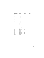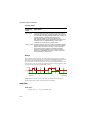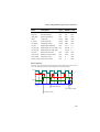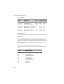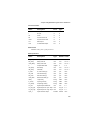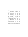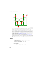
1
SIMETRIX SPICE AND MIXED MODE SIMULATION SIMULATOR REFERENCE MANUAL Copyright ©1992-2010 SIMetrix Technologies Ltd. Trademarks PSpice is a trademark of Cadence Design Systems Inc. Hspice is a trademark of Synopsis Inc. Contact SIMetrix Technologies Ltd., Terence House, 24 London Road, Thatcham, RG18 4LQ, United Kingdom Tel.: Fax: Email: Internet +44 1635 866395 +44 1635 868322 [email protected] http://www.simetrix.co.uk Copyright © SIMetrix Technologies Ltd.. 1992-2010 SIMetrix Simulator Reference Manual 11/5/10 Table of Contents Table of Contents Chapter 1 Introduction Overview.......................................................................... 11 The SIMetrix Simulator - What is it? ................................ 11 What is in This Manual .................................................... 11 Chapter 2 Running the Simulator Using the Simulator with the SIMetrix Schematic Editor.. 12 Adding Extra Netlist Lines ........................................ 12 Displaying Net and Pin Names................................. 12 Editing Device Parameters ....................................... 13 Editing Literal Values - Using shift-F7 ...................... 13 Running in non-GUI Mode ............................................... 14 Overview................................................................... 14 Important Licensing Information ............................... 14 Syntax....................................................................... 14 Aborting .................................................................... 16 Reading Data............................................................ 16 Configuration Settings ..................................................... 16 Netlist Format .................................................................. 19 File Format ............................................................... 20 Language Declaration .............................................. 20 Comments ................................................................ 21 Device Lines ............................................................. 21 Simulator Statements ............................................... 23 Simulator Output.............................................................. 23 The List File .............................................................. 23 The Binary Data File................................................. 24 Output Data Names.................................................. 25 Chapter 3 Simulator Devices Overview.......................................................................... 27 Using XSPICE Devices.................................................... 27 Vector Connections .................................................. 27 Connection Types..................................................... 28 Using Expressions ........................................................... 29 Overview................................................................... 29 Using Expressions for Device Parameters ............... 29 Using Expressions for Model Parameters ................ 30 3 Simulator Reference Manual Expression Syntax ................................................... 30 Optimisation ............................................................. 39 Subcircuits....................................................................... 40 Overview .................................................................. 40 Subcircuit Definition ................................................. 40 Subcircuit Instance................................................... 42 Passing Parameters to Subcircuits .......................... 42 Nesting Subcircuits .................................................. 43 Global Nodes ........................................................... 43 Subcircuit Preprocessing ......................................... 43 Model Binning.................................................................. 44 Overview .................................................................. 44 Defining Binned Models ........................................... 44 Example ................................................................... 44 Language Differences ..................................................... 45 Inline Comment ........................................................ 45 Unlabelled Device Parameters................................. 45 LOG() and PWR() .................................................... 46 Customising Device Configuration .................................. 46 Overview .................................................................. 46 What does the Device Configuration File do?.......... 47 Creating a Device Configuration File ....................... 47 Chapter 4 Analog Device Reference Overview ......................................................................... 52 AC Table Lookup (including S-Parameters).................... 52 AC Table Notes........................................................ 53 Arbitrary Source .............................................................. 53 Notes on Arbitrary Expression ................................. 54 Charge and Flux Devices......................................... 55 Arbitrary Source Examples ...................................... 55 PSpice and Hspice syntax ....................................... 57 Bipolar Junction Transistor (SPICE Gummel Poon)........ 57 Notes........................................................................ 64 Bipolar Junction Transistor (VBIC without self heating) .. 64 Notes........................................................................ 68 Bipolar Junction Transistor (VBIC with self heating) ....... 68 Notes........................................................................ 69 Bipolar Junction Transistor (MEXTRAM) ........................ 69 Bipolar Junction Transistor (HICUM)............................... 70 Capacitor ......................................................................... 70 Current Controlled Current Source.................................. 72 Polynomial Specification .......................................... 73 4 Table of Contents Current Controlled Voltage Source.................................. 74 Current Source ................................................................ 74 Diode - Level 1 and Level 3 ............................................. 75 Diode - Soft Recovery...................................................... 79 Basic Equations........................................................ 80 References ............................................................... 80 GaAsFET ......................................................................... 81 Inductor (Ideal)................................................................. 82 Inductor (Saturable) ......................................................... 83 Notes on the Jiles-Atherton model ........................... 84 Notes on the non-hysteresis model .......................... 85 Implementing Transformers...................................... 85 Plotting B-H curves................................................... 85 References ............................................................... 85 Insulated Gate Bipolar Transistor .................................... 86 Junction FET.................................................................... 87 Lossy Transmission Line ................................................. 89 MOSFET.......................................................................... 91 BSIM3 MOSFETs ............................................................ 98 Notes ........................................................................ 98 Version Selector ....................................................... 98 Model Parameters .................................................... 99 Further Documentation........................................... 100 Process Binning...................................................... 100 BSIM4 MOSFETs .......................................................... 100 Notes ...................................................................... 100 Further Documentation........................................... 101 Process Binning...................................................... 101 EKV MOSFETs.............................................................. 101 Notes ...................................................................... 101 HiSim HV MOSFET ....................................................... 102 Notes ...................................................................... 102 MOSFET GMIN Implementation.................................... 102 PSP MOSFET................................................................ 103 Resistor.......................................................................... 104 Resistor - Hspice Compatible ........................................ 106 Resistance Calculation ........................................... 108 Capacitance Calculation......................................... 109 Temperature Scaling .............................................. 110 ACRESMOD Parameter ......................................... 110 Making the Hspice Resistor the Default ................. 110 S-domain Transfer Function Block ................................ 111 Description.............................................................. 112 Examples................................................................ 112 5 Simulator Reference Manual The Laplace Expression......................................... 115 Defining the Lapalce Expression Using Coefficients116 Other Model Parameters........................................ 116 Limitations .............................................................. 116 The XSPICE S_XFER model ................................. 116 Subcircuit Instance ........................................................ 117 Transmission Line ......................................................... 117 Example ................................................................. 118 Voltage Controlled Current Source ............................... 118 Voltage Controlled Switch ............................................. 119 Voltage Controlled Switch Notes............................ 119 Voltage Controlled Voltage Source ............................... 120 Voltage Source.............................................................. 120 Pulse Source.......................................................... 121 Piece-Wise Linear Source...................................... 123 PWL File Source .................................................... 123 Sinusoidal Source .................................................. 124 Exponential Source ................................................ 125 Single Frequency FM ............................................. 126 Noise Source.......................................................... 126 Extended PWL Source........................................... 126 Mutual Inductor.............................................................. 128 Notes...................................................................... 129 Example ................................................................. 129 Verilog-HDL Interface (VSXA)....................................... 129 Overview ................................................................ 129 Analog Input Interface ............................................ 132 Analog Output Interface ......................................... 133 Data Vector Output ................................................ 133 Module Cache ........................................................ 134 NXP Compact Models ................................................... 135 Introduction ............................................................ 135 Using NXP Devices................................................ 136 Examples ............................................................... 137 Documentation ....................................................... 138 Chapter 5 Digital/Mixed Signal Device Reference Digital Device Overview ................................................ 139 Common Parameters ............................................. 139 Delays .................................................................... 140 And Gate ....................................................................... 140 D-type Latch .................................................................. 142 D-type Flip Flop ............................................................. 144 6 Table of Contents Buffer ............................................................................. 146 Frequency Divider.......................................................... 147 Digital Initial Condition ................................................... 149 Digital Pulse................................................................... 150 Digital Signal Source ..................................................... 151 Inverter........................................................................... 154 JK Flip Flop.................................................................... 155 Arbitrary Logic Block...................................................... 159 Nand Gate ..................................................................... 161 Nor Gate ........................................................................ 162 Open-Collector Buffer .................................................... 163 Open-Emitter Buffer....................................................... 164 Or Gate .......................................................................... 165 Pulldown Resistor .......................................................... 166 Pullup Resistor............................................................... 167 Random Access Memory............................................... 167 Set-Reset Flip-Flop........................................................ 168 SR Latch ........................................................................ 171 State Machine................................................................ 173 Toggle Flip Flop ............................................................. 175 Tri-State Buffer .............................................................. 177 Exclusive NOR Gate...................................................... 179 Exclusive OR Gate ........................................................ 180 Analog-Digital Converter................................................ 181 Analog-Digital Interface Bridge ...................................... 184 Digital-Analog Converter................................................ 188 Digital-Analog Interface Bridge ...................................... 191 Controlled Digital Oscillator ........................................... 194 Analog-Digital Schmitt Trigger ...................................... 196 Chapter 6 Command Reference Overview........................................................................ 198 General Sweep Specification......................................... 199 Overview................................................................. 199 Syntax..................................................................... 200 Multi Step Analyses ....................................................... 201 Overview................................................................. 201 Syntax..................................................................... 201 .AC................................................................................. 202 .ALIAS............................................................................ 204 .DC................................................................................. 205 .FILE and .ENDF ........................................................... 206 .FUNC............................................................................ 207 7 Simulator Reference Manual .GLOBAL ....................................................................... 208 .GRAPH......................................................................... 208 Parameters............................................................. 208 Using Multiple .GRAPH Statements....................... 213 Creating X-Y Plots.................................................. 213 Using .GRAPH in Subcircuits................................. 213 Using Expressions with .GRAPH ........................... 213 Plotting Spectra with .GRAPH................................ 214 .IC.................................................................................. 215 Alternative Initial Condition Implementations ......... 215 .INC ............................................................................... 216 .KEEP............................................................................ 216 .LOAD............................................................................ 218 .LIB ................................................................................ 219 SIMetrix Native Form ............................................. 219 HSPICE Form ........................................................ 220 .MODEL......................................................................... 220 .NOCONV...................................................................... 223 .NODESET .................................................................... 223 .NOISE .......................................................................... 224 .OP ................................................................................ 227 .OPTIONS ..................................................................... 228 .PARAM......................................................................... 241 .POST_PROCESS ........................................................ 244 .PRINT........................................................................... 244 .PZ................................................................................. 246 .SENS............................................................................ 247 .SETSOA....................................................................... 247 Examples ............................................................... 250 .SUBCKT and .ENDS.................................................... 251 .TEMP ........................................................................... 252 .TF ................................................................................. 252 .TRACE ......................................................................... 254 .TRAN............................................................................ 254 Real Time Noise Analysis ............................................. 257 Chapter 7 Monte Carlo Analysis Overview ....................................................................... 259 Specifying a Monte Carlo Run....................................... 259 Specifying a Single Step Monte Carlo Sweep............... 260 Log File.......................................................................... 260 Seeding the Random Number Generator...................... 261 Specifying Tolerances ................................................... 262 8 Table of Contents Overview................................................................. 262 Distribution Functions ............................................. 262 Hspice Distribution Functions ................................. 266 TOL, MATCH and LOT Device Parameters ........... 267 Tolerance Models ................................................... 268 Chapter 8 Convergence and Accuracy Overview........................................................................ 271 DC Operating Point........................................................ 271 Overview................................................................. 271 Source and GMIN Stepping.................................... 272 Pseudo Transient Analysis ..................................... 273 Junction Initialised Iteration .................................... 275 Using Nodesets ...................................................... 275 Transient Analysis ......................................................... 276 What Causes Non-convergence?........................... 276 Fixes for Transient Non-convergence .................... 277 DC Sweep...................................................................... 277 DC Operating Point Algorithms...................................... 277 Junction Initialised Iteration .................................... 278 Source Stepping ..................................................... 278 Diagonal GMIN Stepping........................................ 278 Junction GMIN Stepping......................................... 279 Pseudo Transient Analysis ..................................... 279 Controlling DC Method Sequence .......................... 280 Singular Matrix Errors .................................................... 280 Transient Analysis - ‘Time step too small’ Error ............ 281 Accuracy and Integration Methods ................................ 281 A Simple Approach................................................. 281 Iteration Accuracy................................................... 281 Time Step Control................................................... 282 Accuracy of AC analyses........................................ 284 Summary of Tolerance Options.............................. 284 Integration Methods - METHOD option .................. 285 Chapter 9 Digital Simulation Overview........................................................................ 288 Logic States ................................................................... 288 State resolution table.............................................. 289 Analog to Digital Interfaces............................................ 289 How A-D Bridges are Selected............................... 291 Logic Families................................................................ 291 9 Simulator Reference Manual Logic Family Model Parameters............................. 292 Logic Compatibility Tables ..................................... 292 Logic Compatibility File Format.............................. 293 Supported Logic Families....................................... 294 Universal Logic Family ........................................... 295 Internal Tables ....................................................... 295 Load Delay .................................................................... 295 Overview ................................................................ 295 Output Resistance.................................................. 295 Input Delay ............................................................. 295 Wire Delay.............................................................. 296 Digital Model Libraries................................................... 296 Using Third Party Libraries..................................... 296 Arbitrary Logic Block - User Defined Models................. 296 Overview ................................................................ 296 An Example............................................................ 296 Example 2 - A Simple Multiplier ............................. 299 Example 3 - A ROM Lookup Table ........................ 299 Example 4 - D Type Flip Flop................................. 300 Device Definition - Netlist Entry & .MODEL Parameters 300 Language Definition - Overview ............................. 302 Language Definition - Constants and Names ........ 302 Language Definition - Ports.................................... 302 Language Definition - Registers and Variables...... 304 Language Definition - Assignments ....................... 307 Language Definition - User and Device Values ..... 310 Diagnostics: Trace File........................................... 310 Mixed-mode Simulator - How it Works .......................... 311 Event Driven Digital Simulator ............................... 311 Interfacing to the Analog Simulator ........................ 312 Enhancements over XSPICE ........................................ 312 10 Chapter 1 Introduction Chapter 1 Introduction Overview This manual provides full reference documentation for the SIMetrix simulator. Essentially the simulator receives a netlist as its input and creates a binary data file and list file as its output. The netlist defines the circuit topology and also specifies the analyses to be performed by the simulator. The netlist may directly include any device models required or these may be automatically imported from a device model library. The simulator may be operated in GUI mode or non-GUI mode. GUI mode is the normal method of operation and requires the SIMetrix front end. In non-GUI mode the simulator runs stand alone in a non-interactive fashion and may be set to run at low priority in the background. The SIMetrix Simulator - What is it? The SIMetrix simulator core comprises a direct matrix analog simulator closely coupled with an event driven gate-level digital simulator. This combination is often described as mixed-mode or mixed-signaland has the ability to efficiently simulate both analog and digital circuits together. The core algorithms employed by the SIMetrix analog simulator are based on the SPICE program developed by the CAD/IC group at the department of Electrical Engineering and Computer Sciences, University of California at Berkeley. The digital event driven simulator is derived from XSPICE developed by the Computer Science and Information Technology Laboratory, Georgia Tech. Research Institute, Georgia Institute of Technology. What is in This Manual This reference manual contains detailed descriptions of all simulator analysis modes and supported devices. 11 Simulator Reference Manual Chapter 2 Running the Simulator Using the Simulator with the SIMetrix Schematic Editor Full documentation on using the SIMetrix schematic editor for simulation is described in the SIMetrix User's manual. However, just a few features of the schematic editor are of particular importance for running the simulator and for convenience their description is repeated here. Adding Extra Netlist Lines The analysis mode selected using the schematic editor's Simulator|Choose Analysis... menu is stored in text form in the schematic's simulator command window. If you wish, it is possible to edit this directly. Sometimes this is quicker and easier than using the GUI especially for users who are familiar with the command syntax. Note that the text entered in the simulator command window and the Choose Analysis dialog settings remain synchronised so you can freely switch between the two methods. To open the simulator command window, select the schematic then press the F11 key. It has a toggle action, pressing it again will hide it. If you have already selected an analysis mode using the Choose Analysis dialog, you will see the simulator statements already present. The window has a popup menu selected with the right key. The top item Edit file at cursor will open a text editor with the file name pointed to by the cursor or selected text item if there is one. The simulator command window can be resized using the splitter bar between it and the schematic drawing area. You can add anything you like to this window not just simulator commands. The contents are simply appended to the netlist before being presented to the simulator. So, you can place .PARAM statements, device models, inductor coupling specifications, .OPTION statements or simply comments. The Choose Analysis dialog will parse and possibly modify analysis statements and some .OPTIONS settings but will leave everything else intact. Displaying Net and Pin Names It is sometimes necessary to know the name used for a particular net on the schematic to be referenced in a simulator statement (such as .NOISE) or for an arbitrary source input. There are two approaches: 12 • Find out the default name generated by the schematic editor's netlist generator. To do this, move the mouse cursor over the net of interest then observe the netname in the status bar in the form “NET=???”. • Force a net name of your choice. For this, use a terminal or small terminal symbol. These can be found under the Place|Connectors menu. After placing on Chapter 2 Running the Simulator the schematic, select it then press F7 to edit its name. This name will be used to name the net to which it is connected. Editing Device Parameters To use any of the additional parameters in a schematic, use the Parameters button in the dialog box opened by F7 or the equivalent menu. For example you see this box when editing a resistor Pressing the Parameters button will open another dialog from which you can edit parameter values: You can also bring up this box directly using the right click menu Edit Additional Parameters.... Editing Literal Values - Using shift-F7 The above method is not infallible as it requires the schematic editor to know about the device being edited. In some circumstances, this will require special properties to be present on the symbol and these may have not been defined. (for example something to tell the schematic what level a MOSFET is) 13 Simulator Reference Manual Another situation where the usual device editing methods may be unsuitable is when you need to define a parameter as an expression. In these situations you can use shift-F7. This will edit the device's literal value including any model names exactly as it will be placed in the netlist. shift-F7 bypasses all smart algorithms and presents you with the raw values and you must also supply raw values. For example, here is what you might enter for a MOSFET referencing a model called N1 N1 L={LL-2*EDGE} W={WW-2*EDGE} Note the model name must be included. Running in non-GUI Mode Overview The simulator can be run in a non-interactive non-GUI mode independently of the front end. This is useful for running simulation ‘batches’ controlled by a proprietary script or batch language such as shell scripts or DOS batch files. Under Linux this allows a simulation to be run without an X-server. Under Windows, the simulator will run as a ‘console mode’ application and no GUI elements will be created. When run in this mode, the simulator will read in the specified netlist, run the simulation then close and return control to the calling program. It will generate a binary data file and a list file. Important Licensing Information Non-GUI mode is only possible if you are using network licensing. This feature is not available if you are using a portable (i.e. dongled) license. Please contact support if you have a non-network license and wish to use non-GUI simulation mode. This mode of operation is ‘counted’ for licensing purposes. This means you can only run one non-GUI simulation process for each license issued even if all are run by a single user on a single machine. By contrast, regular simulation initiated manually through the GUI are not counted and any number of runs may be initiated on the same machine by the same user for this purpose. These restrictions have been made to limit exploitation of multiple core machines for simulations run from non-SIMetrix environments. Syntax The command syntax is as follows: SIM [/config "config_location"] [/gui mode] [/check] [/an "analysis_line"] [/list list_filename] [/options "options"] [/nolist] [/lowPriority] [/nodata] [/k] [/extraline extral_line] netlist_file 14 Chapter 2 Running the Simulator [data_file] config_location Location of file holding configuration settings. Configuration settings include global options and global model library locations. The value must be of the form: PATH;pathname pathname may use system symbolic path values such as %EXEPATH%. See User’s Manual for details. If not specified, the configuration settings will be taken from the Base.sxprj file. See the User’s Manual for details on where this file is located. Alternatively, you can specify the location using a setting in the startup.ini file. Add a value called SimConfig to the [Startup] section and give it a value of: PATH;pathname The startup.ini file must be located in the same directory as the SIMetrix executable binary. (SIMetrix.exe on Windows, SIMetrix on Linux). See the User’s Manual for more information on the startup.ini file. Note that the /config switch if present must always appear before the first argument to the command. mode Mode of operation. Default = -1. Valid values are -1, 0, 1 and 2 but only -1 and 1 are meaningful for stand-alone operation. 0 and 2 are used when starting the simulator process from the front end. -1 (same as omitting /gui) runs the simulator in console mode with all messages output to the console or terminal window. 1 enables GUI mode where the simulator runs in a stand-alone mode but displays a graphical status box showing messages and simulator progress. This mode is used by the ‘asynchronous’ menus in the front end. analysis_line If /an switch is specified, analysis_line specifies the analysis to be performed and overrides all analysis lines specified in the netlist. list_filename Name of list file. Default is main netlist file name with extension .OUT. Enclose path name in quotes if it contains spaces. options List of options valid for .OPTIONS statement. netlist_file File name of netlist. data_file File to receive binary data output. /check If specified, the netlist will be read in and parsed but no simulation will be run. Used to check syntax 15 Simulator Reference Manual /nolist If specified, no list file will be created /lowPriority If specified, the simulator will be run as a low priority process, i.e. in the background. Recommended for long runs. /nodata Only vectors explicitly specified using .KEEP or .PRINT will be output to the binary file. Equivalent to ‘.KEEP /nov /noi /nodig’ in the netlist. /k If specified, the program will not finally terminate until the user has pressed enter and a message to that effect will be displayed. Under Windows, if the program is not called from the DOS prompt but from another program, a console will be created for receiving messages. The console will close when the program exits sometimes before the user has had a chance to read the messages. This switch delays the exit of the program and hence the destruction of the console. extra_line An additional line that will be appended to the netlist. This permits simple customisation of the netlist. This should be enclosed in double quotation marks if the line has spaces. Aborting Press cntrl-C - you will be asked to confirm. The simulation will be paused while waiting for your response and will continue if you enter ‘No’. This is an effective means of pausing the run if you need CPU cycles for another task, or you wish to copy the data file. See “Reading Data” below. Reading Data A data file will be created for the simulation results as normal (see “The Binary Data File” on page 24). You can read this file after the simulation is complete use the SIMetrix menu File | Load Data... . You may also read this data file while the simulation is running but you must pause the simulation first using cntrl-C. Important: if you read the data file before the simulation is complete or aborted, the file entries that provide the size of each vector will not have been filled. This means that the waveform viewer will have to scan the whole file in order to establish the size of the vectors. This could take a considerable time if the data file is large. Configuration Settings Configuration settings consist of a number of persistent global options as well as the locations for installed model libraries. When the simulator is run in GUI mode, its configuration settings are controlled by the front end and stored wherever the front end’s settings are stored. See the User's Manual for more details. The settings when run in non-GUI mode are stored in a configuration file which in fact defaults to the same location as the default location for the front end’s settings. You can change this location using the /config switch detailed above (page 14) 16 Chapter 2 Running the Simulator The format of the configuration file is: [Options] option_settings [Models] model_libraries Where: option_settings These are of the form name=value and specify a number of global settings. Boolean values are of the form name= without a value. If the entry is present it is TRUE if absent it is FALSE. Available global settings are detailed below. model_libraries A list of entries specifying search locations for model libraries. These are of the form name=value where name is a string and value is a search location. The string used for name is arbitrary but must be unique. Entries are sorted alphabetically according to the name and used to determine the search order. value is a path name and may contain wildcards (i.e. '*' and '?') 17 Simulator Reference Manual Global Settings Name Type Default Description NoStopOnUnknownParam String WARN Specifies action to be taken in the event of an unknown parameter being encountered in a .MODEL statement. Choices are: TRUE: No action taken, simulation continues normally FALSE: An error will be raised and the simulation will abort WARN: A warning will be displayed but the simulation will continue This will be overridden by a .OPTIONS setting of the same name. See page 235 MaxVectorBufferSize Numeric 32768 See “Data Buffering” below TotalVectorBufferSize Numeric Available RAM/10 See “Data Buffering” below TempDataDir String %STARTDIR% Location of temporary binary data file if data_file is not specified on command line LibraryDiagnostics String Full Controls output of messages relating to model library search. Specify None to disable Data Buffering The simulator buffers data before writing it to disk. By doing so the binary data file can be organised more efficiently allowing data to be recovered from it quickly. There is a relationship between buffer size and read in time as illustrated by the following table. This shows the time taken to read in a 14MByte vector from a 1GByte data file with the system disk cache cleared. The tests were performed with three different buffer sizes on two different systems. One system was an old notebook computer with an IDE disk system. The other was a machine with a high performance SCSI Ultra 320 disk. 18 Chapter 2 Running the Simulator System Buffer size Read time IDE 32768 (default) 8.1 secs Ultra 320 250K 3.1 secs 1 Meg 2.8 secs 32768 (default) 4.1 secs 250K 0.75 secs 1Meg 0.23 secs Note that the buffer size referred to in the above table is for each vector. By default, the simulator won't allocate more than 10% of your system RAM to vector buffers. Clearly if you are running a large circuit and saving many vectors, the buffer sizes could reduce to levels that would make data retrieval very slow. In this case you may wish to consider increasing the memory that is allowed for these buffers. Two configuration settings control the vector buffering. These are: • MaxVectorBufferSize. This sets the maximum size that will be used for any individual vector. The default is 32768 bytes. If you have a high performance SCSI disk system, you may benefit from increasing this value • TotalVectorBufferSize. This sets the maximum amount of memory in bytes used for all buffers. It defaults to a value equal to 10% of your system RAM. This is usually sufficient for most applications but if you are simulating a very large circuit and have sufficient RAM you may like to increase this value The disk will not be written to until the buffers are full. With an all analog circuit all the buffers reach their full state at the same time so they all get written to disk at the same time. If you have 2G of RAM and are simulating a large circuit, approximately 200M of data will be written to the disk at regular intervals. This will result in a pause in the simulation coupled with a great deal of disk activity. Note that both MaxVectorBufferSize and TotalVectorBufferSize may be set from the front end using the Set command. See the User’s Manual for details. Netlist Format The SIMetrix netlist format follows the general format used for all SPICE and SPICE compatible simulators. However, with so many SPICE derivatives and with two significantly different versions of SPICE itself (SPICE 2 and SPICE 3) it is not possible to define a standard SPICE format. SIMetrix has been developed to be as compatible as possible with model libraries that can be obtained from external sources. For discrete devices, models are usually SPICE 2 compatible but some use extensions originally developed for PSpice. IC designers usually receive model files from fabrication companies and these are available for a variety of simulators usually including Hspice. SIMetrix is compatible with all of these but simultaneous compatibility with all formats is not technically possible due to a small number of syntax details - such as the character used for in line comments. To overcome these 19 Simulator Reference Manual minor difficulties, a language declaration can be placed at the top of the netlist and any file included using .INC (page 216) or the Hspice variant of .LIB (page 219). This is described in the following sections. File Format A complete netlist consists of: • A title line • Optional language declaration • Device lines • Statement lines • Comment lines The title line must be the first line of the file and may be empty. The remaining lines with some exceptions - may be placed in any order All other lines are defined by their first non-whitespace character as follows. • Statement lines begin with a period: '.' • Comment lines begin with an asterix: '*' • Device lines begin with a letter A line is usually terminated with a new line character but may be continued using the '+' continuation character. So if the first non-whitespace character is a '+' the line will be considered to be an extension of the previous line. SPICE requires the '+' to be the first character, SIMetrix allows whitespace (space or tab) to precede it. Language Declaration SIMetrix is able to read PSpice, Hspice and native SIMetrix netlists, but in some cases needs to be instructed what format netlist it is reading. Currently there are three areas where simultaneous compatibility has not been possible. These are: • Inline comment character. • Unlabelled device parameters • The meaning of LOG() and PWR() functions SIMetrix can be instructed to use any of the three languages by using the language declaration. This is one of: *#SIMETRIX *#HSPICE *#PSPICE The language declaration must be placed at the top of the file immediately below the title line. It can also be placed in files referenced using .INC or the HSPICE version of .LIB in which case it will apply only to that file and any others that it calls. A language declaration placed anywhere else in a file will be ignored. For details see “Language Differences” on page 45. 20 Chapter 2 Running the Simulator The *#SIMETRIX language declaration can also be supplied with a parameter to specify the separator letter used for devices. See “Device Lines” section below for details. Comments Any line other than a language declaration beginning with a '*' is defined as a comment and will be ignored. Also anything between a semi-colon ';' ('$' in HSPICE mode) and the end of the line will be treated as comment and will also be ignored. Some SPICE simulators require the '*' character to be the first character of the line. SIMetrix allows it to be preceded by white space (spaces and tabs). Device Lines Device lines usually follow the following basic form but each type of device tends to have its own nuances: Name nodelist value [parameters] value may be an actual number e.g. in the case of passive components such as resistors, or it may be a model name in the case of semiconductor devices such as bipolar transistors. Models are defined using a .MODEL statement line. nodelist is a list of netnames. The number and order of these is device dependent. The netname itself may consist of any collection of non-control ASCII characters except whitespace and '.'. All other ASCII characters are accepted although it is suggested that the following characters are avoided if possible: \"%&+-*/^<>[]'@{} If any of these characters are used in a netname, a special syntax will be needed to plot any signal voltage on that net. This is explained in “Output Data Names” on page 25. In addition the characters ‘[‘, ‘]’, ‘%’, ‘!’ and ‘~’ have a special meaning when used with XSPICE devices and therefore should be avoided at all times. The name is the circuit reference of the device. The first letter of this name determines the type of device as shown in the table below. The Pin Names column in the following table is relevant to the vector name used for values of device pin current. See “Output Data Names” on page 25. Letter Number Device of pins Manual Pin Names Page A Any XSPICE devices depends on device B 2 Arbitrary source 53 P, N C 2 Capacitor 70 P, N 21 Simulator Reference Manual Letter Number Device of pins Manual Pin Names Page D 2 Diode 75 P, N E 4 Voltage controlled voltage source 120 P, N, CP, CN F 2 Current controlled current source 72 P, N G 4 Voltage controlled current source 118 P, N, CP, CN H 2 Current controlled voltage source 74 P, N I 2 Fixed current source 74 P, N J 3 JFET 87 D, G, S K 0 Coupling for inductors 128 L 2 Inductor 82 P, N M 4 MOSFET 91 D, G, S, B N - Not used O 4 Lossy transmission line 89 P1, N1, P2, N2 P - Not used Q 3-5 Bipolar transistor 57 C, B, E, S, DT R 2 Resistor 104 P, N S 4 Voltage controlled switch 119 P, N, CP, CN T 4 Lossless transmission line 117 P1, N1, P2, N2 U Any VSXA devices (Verilog-HDL interface), Verilog-A devices, AC Table device V 2 Voltage source 120 P, N W - Not used X Any Subcircuit Y - Not used Z 3 GaAs FET IGBT 117 81 86 D, G, S C, G, E To remove the naming restriction that this system imposes, SIMetrix supports an extension to the above to allow the user to use any name for all devices. If the device letter is followed by a dollar '$' symbol (by default but can be changed - see below), the remainder of the name following the '$' will be used as the device name. E.g.: 22 Chapter 2 Running the Simulator Q$TR23 will define a bipolar transistor with the name TR23. All output generated by the simulator will refer to TR23 not Q$TR23. The above mechanism can be disabled and also the character can be changed by adding a parameter to the language declaration (see page 20). To disable, add this to the top of the netlist: *#SIMETRIX sep=none To change the character use: *#SIMETRIX sep=character character must be a single letter, anything else will be ignored. Although any character will be accepted it should clearly not be alpha-numeric. The above mechanism will also be disabled if HSPICE or PSPICE languages are specified. Simulator Statements Instructions to the simulator other than device definitions and comments are referred to as statements and always begin with a period '.' . Full documentation for SIMetrix statements see “Command Reference” on page 198 Simulator Output The List File SIMetrix produces a list file by default. This receives all text output except for the Monte Carlo log. This includes operating point results, model parameters, noise analysis results, sensitivity analysis results, pole-zero analysis results and tabulated vectors specified by .PRINT. The list file is generated in the same directory as the netlist. It has the same name as the netlist but with the extension .OUT. There are a number of options that control the list file output. 23 Simulator Reference Manual Option name Description PARAMLOG Valid values: Full Given Brief None All instance and model parameter values reported All user specified model parameters and parameterised instance parameters Parameterised model and instance parameters None Default = Given EXPAND Flag. If specified, the netlist with all sub-circuits expanded will be output to the list file EXPANDFILE String. If specified the expand netlist will be output to the specified file rather than the list file NOMOD Same as PARAMLOG=none. Model parameters will not be output WIDTH Page width in number of characters. (The list file is formatted assuming that it will be read or printed using a fixed width font such as Courier.) The default is 80 but any value may be used not just 80 and 132 as in SPICE 2. OPINFO If set DC operating point info file is created for all analyses (except .SENS). Normally it is created only for .OP analyses The Binary Data File The simulation data is stored in a binary data file. The format is proprietary to SIMetrix and is not compatible with SPICE ‘raw’ files. The name and location of the binary file depends on configuration settings and in what mode the simulator is run. Usually, the file is located in the directory specified by the TEMPDATADIR configuration setting (see page 16) and is named according to the analysis type and appended with the extension .sxdat. E.g.tran1.sxdat, ac2.sxdat, dc3.sxdat etc. The name and location can be overridden at the program command line if operated in non-GUI mode or at the front end Run command line if run in GUI mode. Only the SIMetrix front end can read the simulator's binary data file. When run in GUI mode, the file is automatically loaded and in fact it is not usually necessary to know anything about it except perhaps when it grows very large and fills up your disk. If the simulator is run in non-GUI mode, it becomes necessary to explicitly load the data into the front end when the run is complete. This can be done with the command shell menu File|Data|Load…. After the data is loaded, the results can be plotted in the usual manner. See the User's Manual for further details. 24 Chapter 2 Running the Simulator Output Data Names For transient, DC and AC analyses, SIMetrix calculates and stores the circuit’s node voltages and device pin currents and these are all given unique names. If using probing techniques with the front end's schematic editor you don't usually need to know anything about the names used. However there are situations where it is necessary or helpful to know how these names are derived. An example is when compiling an expression relating voltages and currents to be used in a .PRINT statement. Another is when plotting results created by simulating a netlist that was not generated using the schematic editor. The names used are documented in the following notes. Top Level Node Voltages The vector names used for node voltages at the top level (i.e. not in a subcircuit) are simply the name of the node used in the netlist. Subcircuit Node Voltages For nodes within a subcircuit, the name is prefixed with the subcircuit reference and a '.'. For example: X1 N1 N2 N3 SubName X2 N4 N5 N6 SubName .SUBCKT 1 2 3 SubName X3 N1 2 N3 SubName2 R1 VIN 0 1k ... .ENDS .SUBCKT 1 2 3 SubName2 V1 VCC 0 5 ... .ENDS The internal node VIN in definition SubName referenced by X1 would be called X1.VIN. The same node referenced by X2 would be called X2.VIN. The node VCC defined in subcircuit SubName2 would be named X1.X3.VCC and X2.X3.VCC for X1 and X2 respectively. Nodes with Non-standard Names A non-standard node name is one that begins with a digit or which contains one or more of the characters: \"%&+-*/^<>[]'@{} These are legal but introduce problems when accessing the voltage data that they carry. The above characters can be used in arithmetic expressions so cause a conflict if used as a node name. In order to access the voltage data on a node so named, use the Vec() function: Vec('node_name') 25 Simulator Reference Manual Example with .PRINT and node called V+ .PRINT TRAN {Vec('V+')} A similar syntax is required when using the front end plotting commands. Device Pin Currents Device pin currents are named in the following form: device_name#pin_name For primitive devices (i.e. not sub-circuits) pin_name must comply with the table on page 21. For example the current into the collector of Q23 would be Q23#c. The pin names for sub-circuits depend on whether the pinnames: specifier (see “Subcircuit Instance” on page 117) is included in the netlist entry for the device. If it is the pin current name will be the name listed after pinnames:. If it isn't then they are numbered in sequence starting from 1. The order is the same as the order they appear in the netlist device line. For example, if the subcircuit line is: X$U10 N1 N2 N3 N4 N5 LM324 pinnames: VINP VINN VP VN VOUT The current into the last pin (connected to N5) would be U10#VOUT (Note that 'X$' is stripped off as explained above - page 21). If the netlist line is: X$U10 N1 N2 N3 N4 N5 LM324 The same current would be U10#5 Internal Device Values Some devices have internal nodes or sources and the voltages or currents associated with these may be output by the simulator. These are named in a similar manner to pin currents i.e. device_name#internal_name The internal_name depends on the device. For example, bipolar transistors create an internal node for each terminal that specifies a corresponding resistance parameter. So if the RE parameter is specified an internal node will be created called emitter. Note that internal device values are only output if explicitly enabled using the “.KEEP /INTERNAL” statement. See “.KEEP” on page 216 26 Chapter 3 Simulator Devices Chapter 3 Simulator Devices Overview This chapter is an introduction to the “Analog Device Reference” on page 52 and the “Digital/Mixed Signal Device Reference” on page 139. The device reference chapters describe all simulator devices at the netlist level. The netlist consists of a list of component definitions, along with simulator commands, which the simulator can understand. Simple components, such as resistors just need a value to define them. Other more complicated devices such as transistors need a number of parameters to describe their characteristics. The device references includes details of all device and model parameters. Using the schematic editor and model library you may not often need to read this section. Some of the devices, however, have advanced options not directly supported by the user interface. For example, many devices allow a local temperature to be specified. This requires the component value to be appended with TEMP=…. This device parameter and others are documented here. Note that many parts either supplied with SIMetrix or available from component manufacturers are implemented as subcircuits. These are circuit designs to simulate the behaviour of high level devices such as opamps. SIMetrix (and all other SPICE simulators) do not have an opamp device built in but use these macro models instead. Full documentation for these devices is beyond the scope of this manual but can sometimes be obtained from their suppliers. Using XSPICE Devices Some devices are implemented as part of the XSPICE ‘code modelling’ framework. This framework introduces some new features at the netlist level not supported by standard SPICE devices. These new features are described in this section. All but one of these devices that use this framework are digital or mixed signal devices and the reference for these can be found at “Digital/Mixed Signal Device Reference” on page 139. The exception is the “S-domain Transfer Function Block” (page 111) which is a pure analog part. Vector Connections Some models feature an arbitrary number of inputs or/and outputs. For example, an AND gate can have any number of inputs. It would be inflexible to have a separate model for every configuration of AND gate so a method of grouping connections together has been devised. These are known as vector connections. Vector connections are enclosed in square brackets. E.g. the netlist entry for an AND gate is: Axxxx [ in_0 in_1 .. in_n ] out model_name 27 Simulator Reference Manual The pins in_0 in_1 to in_n form a single vector connection. Any number of pins may be placed inside the square brackets, in fact the same model may be used for devices with different numbers of inputs. Some devices have a minimum and/or maximum number of pins that may be used in a vector connection. This is known as vector bounds and if they apply will be listed in the vector bounds column of the Connection Details table provided with every device definition. Connection Types In the device references that follow, each has a table titled Connection Details. Each table has a “Type” column and some have an “Allowed types” column. The type referred to here is the type of electrical connection e.g. voltage, current, differential or single-ended. Some devices allow some or all of their connections to be specified with a range of types. For example, the analog-digital converter described on page 181 has a single ended voltage input by default. However, using a simple modification to the netlist entry, an ADC can be specified with a differential voltage input or even a differential current. Changing the type of connection involves no changes to the .MODEL statement, only to the netlist entry. The following table lists all the available types. The modifier is the text used to alter a connection type at the netlist level. This is explained below Description Modifier Single ended voltage %v Single ended current %i Differential voltage %vd Differential current %id Digital %d Grounded conductance (voltage input current output) %g Grounded resistance (current input, voltage output) %h Differential conductance (voltage input current output) %gd Differential resistance (voltage input current output) %hd With the models supplied with SIMetrix, only the first four in the above table are ever offered as options. The others are used but are always compulsory, and an understanding of their meaning is not necessary to make full use the system. As well as type, all connections also have a flow referring to the direction of the signal flow. This can be in, out or inout. Voltage, current and digital connections may be in or out while the conductance and resistance connections may only be inout. Voltage inputs are always open circuit, current inputs are always short circuit, voltage outputs 28 Chapter 3 Simulator Devices always have zero output impedance and current outputs always have infinite output impedance. The conductance connections are a combined voltage input and current output connected in parallel. If the output is made to be proportional to the input, the connection would be a conductor with a constant of proportionality equal to its conductance, hence the name. Similarly, the resistance connections are a combined current input and voltage output connected in series. If the output is made to be proportional to the input, the connection would be a resistor with a constant of proportionality equal to its resistance. Changing Connection Type If a model allows one or more of its connections to be given a different type, this can be done by preceding the connection entry with the appropriate modifier listed in the table above. For example if you wish to specify a 4 bit ADC with a differential voltage input, the netlist entry would be something like: A1 %vd ANALOG_INP ANALOG_INN CLOCK_IN [ DATA_OUT_0 DATA_OUT_1 DATA_OUT_2 DATA_OUT_3 ] DATA_VALID ADC_4 Using Expressions Overview Expressions consist of arithmetic operators, functions, variables and constants and may be employed in the following locations: • As device parameters • As model parameters • To define a variable (see “.PARAM” on page 241) which can itself be used in an expression • As the governing expression used for arbitrary sources (see page 53). They have a wide range of uses. For example: • To define a number of device or model parameters that depend on some common characteristic. This could be a circuit specification such as the cut-off frequency of a filter or maybe a physical characteristic to define a device model. • To define tolerances used in Monte Carlo analyses. • Used with an arbitrary source, to define a non-linear device. Using Expressions for Device Parameters Device or instance parameters are placed on the device line. For example the length parameter of a MOSFET, L, is a device parameter. A MOSFET line with constant parameters might be: M1 1 2 3 4 MOS1 L=1u W=2u 29 Simulator Reference Manual L and W could be replaced by expressions. For example M1 1 2 3 4 MOS1 L={LL-2*EDGE} W={WW-2*EDGE} Device parameter expressions must usually be enclosed with either single quotation marks ( ' ) double quotation marks ( " ) or braces ( '{' and '}' ). The expression need not be so enclosed if it consists of a single variable. For example: .PARAM LL=2u WW=1u M1 1 2 3 4 MOS1 L=LL W=WW Using Expressions for Model Parameters The rules for using expressions for device parameters also apply to model parameters. E.g. .MODEL N1 NPN IS=is BF={beta*1.3} Expression Syntax The expression describing an arbitrary source consists of the following elements: • Circuit variables • Parameters • Constants. • Operators • Functions • Look up tables These are described in the following sections Circuit Variables Circuit variables may only be used in expressions used to define arbitrary sources and to define variables that themselves are accessed only in arbitrary source expressions. Circuit variables allow an expression to reference voltages and currents in any part of the circuit being simulated. Voltages are of the form: V(node_name1) OR V(node_name1, node_name2) Where node_name1 and node_name2 are the name of the node carrying the voltage of interest. The second form above returns the difference between the voltages on node_name1 and node_name2. If using the schematic editor nodenames are normally 30 Chapter 3 Simulator Devices allocated by the netlist generator. For information on how to display and edit the schematic's node names, refer to “Displaying Net and Pin Names” on page 12. Currents are of the form: I(source_name) Where source_name is the name of a voltage source carrying the current of interest. The source may be a fixed voltage source, a current controlled voltage source, a voltage controlled voltage source or an arbitrary voltage source. It is legal for an expression used in an arbitrary source to reference itself e.g.: B1 n1 n2 V=100*I(B1) Implements a 100 ohm resistor. Parameters These are defined using the .PARAM statement. See page 241 for details. For example .PARAM res=100 B1 n1 n2 V=res*I(B1) Also implements a 100 ohm resistor. Circuit variables may be used .PARAM statements, for example: .PARAM VMult = { V(a) * V(b) } B1 1 2 V = Vmult + V(c) Parameters that use circuit variables may only be used in places where circuit variables themselves are allowed. So, they can be used in arbitrary sources and they may be used to define the resistance of an Hspice style resistor which allows voltage and current dependence. (See “Resistor - Hspice Compatible” on page 106). They may also of course be used to define further parameters as long as they too comply with the above condition. Built-in Parameters A number of parameter names are assigned by the simulator. These are: 31 Simulator Reference Manual Parameter name Description TIME Resolves to time for transient analysis. Resolves to 0 otherwise including during the pseudo transient operation point algorithm. Note that this may only be used in an arbitrary source expression TEMP Resolves to current circuit temperature in Celcius HERTZ Resolves to frequency during AC sweep and zero in other analysis modes PTARAMP Resolves to value of ramp during pseudo transient operating point algorithm if used in arbitrary source expression. Otherwise this value resolves to 1. Constants Apart from simple numeric values, arbitrary expressions may also contain the following built-in constants: Constant name Value Description PI 3.14159265358979323846 E 2.71828182845904523536 e TRUE 1.0 FALSE 0.0 ECHARGE 1.6021918e-19 Charge on an electron in coulombs BOLTZ 1.3806226e-23 Boltzman's constant If the simulator is run from the front end in GUI mode, it is also possible to access variables defined on the Command Shell command line or in a script. The variable must be global and enclosed in braces. E.g. B1 n1 n2 V = V(n3, n3) * { global:amp_gain } amp_gain could be defined in a script using the LET command. E.g. “Let global:amp_gain = 100” Operators These are listed below and are listed in order of precedence. Precedence controls the order of evaluation. So 3*4 + 5*6 = (3*4) + (5*6) = 42 and 3+4*5+6 = 3 + (4*5) + 6 = 29 as '*' has higher precedence than '+'. 32 Chapter 3 Simulator Devices Operator Description ~!- Digital NOT, Logical NOT, Unary minus ^ or ** Raise to power. *, / Multiply, divide +, - Plus, minus >=, <=, > < Comparison operators ==, != or <> Equal, not equal & Digital AND (see below) | Digital OR (see below) && Logical AND || Logical OR test ? true_expr : Ternary conditional expression (see below) false_expr Comparison, Equality and Logical Operators These are Boolean in nature either accepting or returning Boolean values or both. A Boolean value is either TRUE or FALSE. FALSE is defined as equal to zero and TRUE is defined as not equal to zero. So, the comparison and equality operators return 1.0 if the result of the operation is true otherwise they return 0.0. The arguments to equality operators should always be expressions that can be guaranteed to have an exact value e.g. a Boolean expression or the return value from functions such as SGN. The == operator, for example, will return TRUE only if both arguments are exactly equal. So the following should never be used: v(n1)==5.0 v(n1) may not ever be exactly 5.0. It may be 4.9999999999 or 5.00000000001 but only by chance will it be 5.0. These operators are intended to be used with the IF() function described below. Digital Operators These are the operators '&', '|' and '~'. These were introduced in old SIMetrix version as a simple means of implementing digital gates in the analog domain. Their function has largely been superseded by gates in the event driven simulator but they are nevertheless still supported. Although they are used in a digital manner the functions implemented by these operators are continuous in nature. They are defined as follows: 33 Simulator Reference Manual Expression Condition Result out = x & y x<vtl OR y<vtl x>vth AND y>vth x>vth AND vth>y>vtl vtl<x< vth AND y>vth vtl<x< vth AND vth>y>vtl out = vl out = vh out = (y-vtl)*(vh-vl)/(vth-vtl)+vl out = (x-vtl)*(vh-vl)/(vth-vtl)+vl out = (y-vtl)*(x-vtl)*(vh-vl)/(vthvtl)2+vl out = x|y x<vtl AND y<vtl x>vth OR y>vth x<vtl AND vth>y>vtl vtl<x< vth AND y<vtl vtl<x< vth AND vth>y>vtl out = vl out = vh out = vh-(vth-y)*(vh-vl)/(vth-vtl) out = vh-(vth-x)*(vh-vl)/(vth-vtl) out = vh-(vth-y)*(vth-x)*(vh-vl)/ (vth-vtl)2 out = ~x x<vtl x>vth vtl<x< vth out = vh out = vl out = (vth-x)/(vth-vtl)*(vh-vl)+vl Where: vth = upper input threshold vtl = lower input threshold vh = output high vl = output low These values default to 2.2, 2.1, 5 and 0 respectively. These values are typical for high speed CMOS logic (74HC family). They can be changed with four simulator options set by the .OPTIONS simulator statement. These are respectively, LOGICTHRESHHIGH, LOGICTHRESHLOW, LOGICHIGH, LOGICLOW To change the lower input threshold to 1.9, add the following line to the netlist: .OPTIONS LOGICTHRESHLOW=1.9 To find out how to add additional lines to the netlist when using the schematic editor, refer to “Adding Extra Netlist Lines” on page 12. Ternary Conditional Expression This is of the form: test_expression ? true_expression : false_expression The value returned will be true_expression if test_expression resolves to a non-zero value, otherwise the reurn value will be false_expression. This is functionally the same as the IF() function described in the functions table below. 34 Chapter 3 Simulator Devices Functions Function Description ABS(x) Magnitude of x. if x>=0 result=x otherwise result=-x ACOS(x), ARCCOS(x) Arc cosine. Result is in radians ACOSH(x) Inverse COSH ASIN(x), ARCSIN(x) Arc sine. Result is in radians ASINH(x) Inverse SINH ATAN(x), ARCTAN(x) Arc tangent. Result is in radians ATAN2(x,y) =ATAN(x/y). Valid if y=0. Result in radians ATANH(x) Inverse TANH COS(x) Cosine of x in radians COSH(x) Hyperbolic cosine DDT(x) Differential of x with respect to time EXP(x) ex FLOOR(x), INT(x) Next lowest integer of x. IF(cond, x, y) if cond is TRUE result=x else result=y IFF(cond, x, y) As IF(cond, x, y) LIMIT(x, lo, hi) if x<lo result=lo else if x>hi result=hi else result=x LN(x) Log to base e of x. If x<10-100 result=-230.2585093 LOG(x) Log to base 10 of x. If x<10-100 result=-100 LOG10(x) Log to base 10 of x. If x<10-100 result=-100 MAX(x, y) Returns larger of x and y MIN(x,y) Returns smaller of x and y PWR(x,y) |x|y PWRS(x,y) if x>=0 |x|y else -|x|y SDT(x) Integral of x with respect to time SGN(X) If x>0 result = 1 else if x<0 result = -1 else result = 0 SIN(x) Sine of x in radians SINH(x) Hyperbolic sine SQRT(x) if x>=0 x else -x STP(x) If x<=0 result = 0 else result = 1 35 Simulator Reference Manual Function Description TAN(x) Tangent of x in radians TANH(x) Hyperbolic tangent U(x) as STP(x) URAMP(x) if x<0 result =0 else result = x Monte Carlo Distribution Functions To specify Monte Carlo tolerance for a model parameter, use an expression containing one of the following 12 functions: Name Distribution Lot? GAUSS Gaussian No GAUSSL Gaussian Yes UNIF Uniform No UNIFL Uniform Yes WC Worst case No WCL Worst case Yes GAUSSE Gaussian logarithmic No GAUSSEL Gaussian logarithmic Yes UNIFE Uniform logarithmic No UNIFEL Uniform logarithmic Yes WCE Worst case logarithmic No WCEL Worst case logarithmic Yes A full discussion on the use of Monte Carlo distribution functions is given in “Specifying Tolerances” on page 262 Look-up Tables Expressions may contain any number of look-up tables. This allows a transfer function of a device to be specified according to - say - measured values without having to obtain a mathematical equation. Look-up tables are specified in terms of x, y value pairs which describe a piece-wise linear transfer function. Look up tables are of the form: TABLE[ xy_pairs ]( input_expression ) 36 Chapter 3 Simulator Devices Where: xy_pairs A sequence of comma separated pairs of constant values that define the input and output values of the table. For each pair, the first value is the x or input value and the second is the y or output value. Only explicit numeric constants may be used. Even internal constants such as PI may not be used. input_expression Expression defining the input or x values of the table. Example The following arbitrary source definition implements a soft limiting function B1 n2 n3 V=table[-10, -5, -5, -4, -4, -3.5, -3, -3, 3, 3, 4, 3.5, 5, 4, 10, 5](v(N1)) and has the following transfer function: 4 :b1_p / V 2 0 -2 -4 -20 v1/V -15 -10 -5 0 5 10 15 5V /div It is possible to assign expressions to component values which are evaluated when the circuit is simulated. This has a number of uses. For example you might have a filter design for which several component values affect the roll off frequency. Rather than recalculate and change each component every time you wish to change the roll of frequency it is possible to enter the formula for the component's value in terms of this frequency. 37 Simulator Reference Manual Example {C1} C1 {2/(2*pi*f 0*C1*alpha)} {2/(2*pi*f 0*C1*alpha)} R2 1 VOUT R1 AC 1 0 V1 E1 {C1*alpha*alpha/4} C2 The above circuit is that of a two pole low-pass filter. C1 is fixed and R1=R2. The design equations are: R1=R2=2/(2*pi*f0*C1*alpha) C2=C1*alpha*alpha/4 where f0 is the cut off frequency and alpha is the damping factor. The complete netlist for the above circuit is: V1 C2 C1 E1 R1 R2 V1_P 0 AC 1 0 0 R1_P {C1*alpha*alpha/4} VOUT R1_N {C1} VOUT 0 R1_P 0 1 R1_P R1_N {2/(2*pi*f0*C1*alpha)} R1_N V1_P {2/(2*pi*f0*C1*alpha)} Before running the above circuit you must assign values to the variables. This can be done by one of three methods: • With the .PARAM statement placed in the netlist. • With Let command from the command line or from a script. (If using a script you must prefix the parameter names with global:) • By sweeping the value with using parameter mode of a swept analysis (page 199) or multi-step analysis (page 201). Expressions for device values must be entered enclosed in curly braces ('{' and '}'). Suppose we wish a 1kHz roll off for the above filter. Using the .PARAM statement, add these lines to the netlist .PARAM f0 1k .PARAM alpha 1 .PARAM C1 10n For more information on .PARAM see page 241 38 Chapter 3 Simulator Devices Using the Let command, you would type: Let f0=1k Let alpha=1 Let C1=10n If you then wanted to alter the damping factor to 0.8 you only need to type in its new value: Let alpha=0.8 then re-run the simulator. To execute the Let commands from within a script, prefix the parameter names with global:. E.g. “Let global:f0=1k” In many cases the .PARAM approach is more convenient as the values can be stored with the schematic. Optimisation Overview An optimisation algorithm may be enabled for expressions used to define arbitrary sources and any expression containing a swept parameter. This can improve performance if a large number of such expressions are present in a design. The optimiser dramatically improves the simulation performance of the power device models developed by Infineon. See “Optimiser Performance” below. Why is it Needed? The simulator’s core algorithms use the Newton-Raphson iteration method to solve non-linear equations. This method requires the differential of each equation to be calculated and for arbitrary sources, this differentiation is performed symbolically. So as well calculating the user supplied expression, the simulator must also evaluate the expression’s differential with respect to each dependent variable. These differential expressions nearly always have some sub-expressions in common with subexpressions in the main equation and other differentials. Calculation speed can be improved by arranging to evaluate these sub-expressions only once. This is the main task performed by the optimiser. However, it also eliminates factors found on both the numerator and denominator of an expression as well as collecting constants together wherever possible. Using the Optimiser The optimiser will automatically be enabled for any arbitrary source or swept expression that uses a function defined using .FUNC (see “.FUNC” on page 207). To enable for all expressions, use the following option setting: .OPTIONS optimise=2 Conversely, optimisation can be disable completely with: 39 Simulator Reference Manual .OPTIONS optimise=0 Optimiser Performance The optimisation algorithm was added to SIMetrix primarily to improve the performance of some publicly available power device models from Infineon. These models make extensive use of arbitrary sources and many expressions are defined using .FUNC. The performance improvement gained for these model is in some cases dramatic. For example a simple switching PSU circuit using a SGP02N60 IGBT ran around 5 times faster with the optimiser enabled and there are other devices that show an even bigger improvement. Accuracy The optimiser simply changes the efficiency of evaluation and doesn’t change the calculation being performed in any way. However, performing a calculation in a different order can alter the least significant digits in the final result. In some simulations, these tiny changes can result in much larger changes in circuit solution. So, you may find that switching the optimiser on and off may change the results slightly. Subcircuits Overview Subcircuits are a method of defining a circuit block which can be referenced any number of times by a single netlist line or schematic device. Subcircuits are the method used to define many device models such as op-amps. Subcircuit Definition Subcircuits begin with the .SUBCKT statement and end with .ENDS. A subcircuit definition is of the form: .SUBCKT subcircuit_name nodelist [[params:] default_parameter_list] definition_lines .ENDS 40 subcircuit_name Name of the subcircuit and is used to reference it in the main netlist. nodelist Any number of node names and are used for external connections. The subcircuit call (using an ‘X’ device) would use a matching number of nodes in the same order. default_parameter_list List of parameters and their default values in the form name=value. Subcircuit parameters are explained in “Using Expressions” on Chapter 3 Simulator Devices page 29. definition_lines List of valid device and model lines. In addition, .NODESET, .IC and .KEEP lines may also be placed in a subcircuit. Example This is an example of an opamp subcircuit called SXOA1000. VINP, VINN VOUT VCC and VEE are its external connections. The three .model lines define devices that are local, that is, they are only accessible within the subcircuit definition. .subckt SXOA1000 VINP VINN VOUT VCC VEE I2 D2_N VEE 100u I1 Q3_E VEE 100u C1 VOUT R1_P 10p D1 Q7_C D1_N D1 D2 D1_N D2_N D1 D3 VEE Q3_E D1 Q2 VEE D2_N VOUT 0 P1 Q3 Q3_C R3_P Q3_E 0 N1 Q1 VCC Q7_C VOUT 0 N1 Q6 Q3_C Q3_C VCC 0 P1 Q7 Q7_C Q5_C VCC 0 P1 R1 R1_P Q5_C 100 Q4 Q5_C R2_N Q3_E 0 N1 R2 VINP R2_N 1K Q5 Q5_C Q3_C VCC 0 P1 R3 R3_P VINN 1K .model N1 NPN VA=100 TF=1e-9 .model P1 PNP VA=100 TF=1e-9 .model D1 D .ends Where to Place Subcircuit Definition Subcircuit definitions may be placed in a number of locations. • Directly in the netlist. This is the best place if the subcircuit is specific to a particular design. If you are entering the circuit using the schematic editor, see “Adding Extra Netlist Lines” on page 12. to find out how to add additional lines to the netlist. • Put in a separate file and pull in to the schematic with .INC (page 216) statement placed in the netlist. • Put in a library file and reference in schematic with SIMetrix form of .LIB (page 219) statement placed in the netlist. Similar to 2. but more efficient if library has many models not used in the schematic. Only the devices required will be read in. • Put in a library file and install as a model library. See User's Manual for full details. 41 Simulator Reference Manual Subcircuit Instance Once a subcircuit has been defined, any number of instances of it may be created. These are of the form: Xxxxx nodelist sub_circuitname [ [params:|:] parameters] nodelist List of nodes, each of which will connect to its corresponding node in the subcircuit's definition. The number of nodes in the instance must exactly match the number of nodes in the definition. sub_circuitname Name of the subcircuit definition. parameters List of parameter names and their values in the form name=value. These may be referenced in the subcircuit definition. Subcircuit parameters are explained below. Passing Parameters to Subcircuits You can pass parameters to a subcircuit. Consider the filter example provided in “Using Expressions” above. Supposing we wanted to define several filters with different characteristics. We could use a subcircuit to define the filter but the values of the components in the filter need to be different for each instance. This can be achieved by passing the parameter values to each instance of the subcircuit. So: ** Definition .SUBCKT Filter IN OUT params: C1=1n alpha=1 f0=1k C2 0 R1_P {C1*alpha*alpha/4} C1 OUT R1_N {C1} E1 OUT 0 R1_P 0 1 R1 R1_P R1_N {2/(2*pi*f0*C1*alpha)} R2 R1_N IN {2/(2*pi*f0*C1*alpha)} .ENDS ** Subcircuit instance X1 V1_P VOUT Filter : C1=10n alpha=1 f0=10k ** AC source V1 V1_P 0 AC 1 0 In the above example the parameters after params: in the .subckt line define default values should any parameters be omitted from the subcircuit instance line. It is not compulsory to define defaults but is generally recommended. Note In the syntax definition for both subcircuit definitions and subcircuit instances, the params: specifier is shown as optional. If params: is included the '=' separating the parameter names and their values becomes optional. 42 Chapter 3 Simulator Devices Nesting Subcircuits Subcircuit definitions may contain both calls to other subcircuits and local subcircuit definitions. If a subcircuit definition is placed within another subcircuit definition, it becomes local. That is, it is only available to its host subcircuit. Calls to subcircuits may not be recursive. A subcircuit may not directly or indirectly call its own definition. Global Nodes Sometimes it is desirable to refer to a node at the circuit's top level from within a subcircuit without having to explicitly pass it. This is sometimes useful for supply rails. SIMetrix provides three methods. • '#' prefix. Any node within a subcircuit prefixed with '#' will connect to a top level node of the same name without the '#' prefix. • '$g_' prefix. Any node in the circuit prefixed '$g_' will be treated as global • Using .GLOBAL see page 208 The second approach is compatible with PSpice. The third approach is compatible with Hspice Note the first two approaches are subtly different. In the second approach the '$g_' prefix must be applied to all connected nodes, whereas in the first approach the '#' prefix must be applied only to subcircuit nodes. Subcircuit Preprocessing SIMetrix features a netlist preprocessor that is usually used for SIMPLIS simulations and was developed for that purpose. The preprocessor has some features that aren’t available in the native simulator and for this reason it would be useful to be able to use the preprocessor for SIMetrix simulations. It is not necessary to apply the preprocessor to the entire netlist. Any subcircuit call that defines preprocessor variables using the ‘vars:’ specifier will be passed to the preprocessor. For example: X$C1 R1_P 0 ELEC_CAP_L13 vars: LEVEL=3 CC=1m + RSH_CC=1Meg IC=0 RESR=10m LESL=100n USEIC=1 calls the ELEC_CAP_L13 subcircuit but passes it through the preprocessor first. This model is a model for an electrolytic capacitor and uses a number of .IF statements to select model features according to the LEVEL parameter. The preprocessor also provides a means of generating multiple devices using .WHILE. For information on the preprocessor, see the SIMPLIS Reference Manual. A PDF version of this is available on the install CD. 43 Simulator Reference Manual Model Binning Overview Some devices can be binned. This means that a number of different model definitions can be provided for the same device with each being valid over a limited range of some device parameter or parameters. The simulator will automatically select the appropriate model according to the value given for the device parameters. Currently only BSIM3, BSIM4 and HiSIM HV MOSFETs may be binned. The binning is controlled by the length and width device parameters (L and W) while the LMIN, LMAX, WMIN and WMAX model parameters specify the valid range for each model. Important Note The binned models should be placed directly in the netlist or called using either .INC or the Hspice form of .LIB. They will not work correctly when installed as a model library or accessed with the SIMetrix form of .LIB. Defining Binned Models Binned models are defined as a set consisting of two or more .MODEL definitions. Each of the definitions must be named using the following format: root_name.id root_name Name used by the device to call the model. Must be the same for all model definitions in a set id Arbitrary name that must be unique for each model in a set. This would usually be a number but this is not a requirement Each model definition must also contain a MIN/MAX parameter pair for each bin control parameter. For the BSIM3 MOSFET there are two bin control parameters, namely L and W with corresponding MIN/MAX pairs LMIN/LMAX and WMIN/ WMAX. For a binned BSIM3 model, all four must be present. These parameters define the range of L and W over which the model is valid. When a model is required, the simulator searches all models with the same root_name for a definition whose LMIN/ LMAX and WMIN/WMAX parameters are compatible with the device's L and W. Example .MODEL N1.1 NMOS LEVEL=49 ... parameters ... + LMIN=1u LMAX=4u WMIN=1u WMAX=4u .MODEL N1.2 NMOS LEVEL=49 ... parameters ... + LMIN=4u LMAX=10u WMIN=1u WMAX=4u .MODEL N1.3 NMOS LEVEL=49 ... parameters ... + LMIN=1u LMAX=4u WMIN=4u WMAX=10u .MODEL N1.4 NMOS LEVEL=49 ... parameters ... + LMIN=4u LMAX=10u WMIN=4u WMAX=10u 44 Chapter 3 Simulator Devices ** This device will use N1.1 M1 1 2 3 4 N1 L=2u W=2u ** This device will use N1.2 M2 1 2 3 4 N1 L=6u W=2u ** This device will use N1.3 M3 1 2 3 4 L=2u W=7u ** This device will use N1.4 M4 1 2 3 4 L=6u W=7u Language Differences SIMetrix is compatible with some PSpice and Hspice extensions mainly so that it can read external model files. Some aspects of these alternative formats are incompatible with the SIMetrix native format and in such cases it is necessary to declare the language being used. See “Language Declaration” on page 20 for details on how to do this. The following sections describe the incompatibilities between the three languages. Inline Comment Hspice uses the dollar ('$') symbol for inline comments while SIMetrix and PSpice use a semi-colon (';'). The language declaration described above determines what character is used. Unlabelled Device Parameters The problem with unlabelled device parameters is illustrated with the following examples. The following lines are legal in Hspice mode but illegal in SIMetrix mode. .PARAM area=2 Q1 C B E S N1 area Q1 will have an area of 2. Conversely the following is legal in SIMetrix but is illegal in Hspice: .PARAM area=2 Q1 C B E S N1 area area Again Q1 has an area of 2. The problem is that SIMetrix does not require '=' to separate parameter names with their values whereas Hspice does. area is a legal BJT parameter name so in the first example SIMetrix can't tell whether area refers to the name of the BJT parameter or the name of the .PARAM parameter defined in the previous line. Hspice can tell the difference because if area meant the BJT parameter name it would be followed by an '='. This line is legal and will be correctly interpreted in both modes 45 Simulator Reference Manual .PARAM area=2 Q1 C B E S N1 area=area Although Hspice always requires the '=' to separate parameter names and values, it continues to be optional in SIMetrix even in Hspice mode. It only becomes compulsory where an ambiguity needs to be resolved as in the second example above. LOG() and PWR() The LOG() function means log to the base 10 in SIMetrix but in PSpice and Hspice means log to the base e. PWR() in PSpice and SIMetrix means |x|y whereas in Hspice it means “if x>=0 |x|y else -|x|y”. The language declaration only affects the definition when used in expressions to define model and device parameters. When used in arbitrary source expressions, the language assumed is controlled by the method of implementing the device as follows: SIMetrix: B1 1 2 V=expression PSpice E1 1 2 VALUE = {expression } Hspice E1 1 2 VOL = 'expression' Note that the function LN() always means log to base e and LOG10() always means log to base 10. We recommend that these functions are always used in preference to LOG to avoid confusion. Customising Device Configuration Overview Models for discrete devices and for integrated circuit processes come from a variety of sources and are often designed for particular simulators, in particular, PSpice and Hspice. These simulators are not generally compatible with each other so it is not easy for SIMetrix to be simultaneously compatible with both. Further, SIMetrix itself needs to retain backward compatibility with its own earlier versions. An example of conflict can be found with the standard diode. The SIMetrix diode with no level parameter specified is mainly compatible with PSpice. But the standard Hspice diode is quite different and not compatible. The SIMetrix Level=3 diode is however compatible with Hspice both for level=1 and level=3. To use Hspice level=1 diode models the user has to edit the model so that level is changed to 3. It is not always convenient to modify model files and for this reason SIMetrix provides an alternative in the form of the device configuration file. This provides a means of changing the access to particular device model including re-mapping level numbers. The following section describes how to setup a device configuration file. 46 Chapter 3 Simulator Devices What does the Device Configuration File do? The device configuration file (DCF) edits or adds to an internal table used to map model names, level numbers and access letters to an actual device model. All device models (that is the binary code that implements the device equations) have an internal name that is used to uniquely identify it, but this name is not used externally. Instead .MODEL statements use their own name (e.g. nmos, pnp) coupled with an optional LEVEL parameter to define the actual device referred to. For example, the MOS level 3 device is referred internally as “MOS3” but the .MODEL statements use the names NMOS or PMOS and set the LEVEL parameter to 3. The mapping between NMOS and LEVEL 3 to “MOS3” is defined in an internal table which can be modified by specifying a device configuration file. The DCF can add new entries to the table so providing additional methods of accessing a device. It can also modify existing entries to point to a new device. Creating a Device Configuration File The device configuration file (DCF) path and name are defined by the option variable DevConfigFile. By ‘option variable’, we mean the variables assigned using the command line Set command not simulator options set by .OPTIONS. The default value for the setting is %SHAREPATH%/DeviceConfig.sxdcf, %SHAREPATH% resolves to the support directory under the SIMetrix root in windows and the share directory in Linux. Format Each line in the DCF maps a single device and consists of up to 4 assigned parameters. These are described in the following table. Keyword Description ModelName Model name used in .MODEL statement Device Internal device name. See table Level Level parameter Letter Device letter To modify an existing mapping, you only need to provide the model name, device and level. The modelname and level must point to an existing combination that is already in use (see table on page 48), e.g. ModelName=D and Level=1, and device would then be set to the new device that this combination is to point to, e.g. Diode3. So this is what the line would be: ModelName=D,Level=1,Device=Diode3 The above would make level 1 diodes use the same model as level=3. Here is another example: ModelName=R,Level=0,Device=HspiceRes 47 Simulator Reference Manual Level=0 is the level value when the LEVEL parameter is not specified. In the case of resistors, no .MODEL statement is required at all, so the above line will change the default model used for all resistors to the Hspice model instead of the native SIMetrix model. It is also possible to add a new mapping in which case the level and modelname parameters must be currently unused. Also when creating a new mapping the ‘Letter’ parameter must be specified. ‘Letter’ is the first letter of the component reference traditionally used to identify the type of device in SPICE netlists. For example ‘Q’ refers to BJTs and ‘D’ refers to diodes. For example, the following entries define LEVEL=55 as a valid level for accessing the EKV model: ModelName=NMOS,Level=55,Device=EKV,Letter=M ModelName=PMOS,Level=55,Device=EKV,Letter=M Note that two entries are required in order to support both n-channel and p-channel devices. The above doesn’t change the existing level (44) it adds an additional level. Both 44 and 55 will be accepted and be equivalent. When defining a new mapping the letter must be specified and usually this should be the letter conventionally used for the class of device. If defining a new mapping for a MOSFET, the letter ‘M’ should be used, for a diode the letter ‘D’ should be used and so on. However, the letters, ‘N’, ‘P’, ‘W’, ‘U’ and ‘Y’ maybe used as well for any type of device. The following table shows all built in device mappings. Note that this describes devices that are built in to the simulator binary. A number of devices are defined in external DLLs. Mappings for these are shown in the next table. Device Mappings for Internal Devices 48 ModelName Device Level Letter npn BJT 0 Q pnp BJT 0 Q npn BJT 1 Q pnp BJT 1 Q lpnp BJT 0 Q lpnp BJT 1 Q d Diode 0 D d Diode 1 D d Diode3 3 D njf JFET2 0 J Chapter 3 Simulator Devices ModelName Device Level Letter njf JFET 1 J pjf JFET2 0 J pjf JFET 1 J nmf MES 0 Z pmf MES 0 Z nmos Mos1 0 M nmos Mos1 1 M nmos Mos2 2 M nmos Mos3 3 M nmos Vmos 17 M pmos Mos1 0 M pmos Mos1 1 M pmos Mos2 2 M pmos Mos3 3 M pmos Vmos 17 M r Resistor 0 R res Resistor 0 R r HspiceRes 2 R c Capacitor 0 C cap Capacitor 0 C sw Switch 0 S vswitch Switch 0 S ltra LTRA 0 O vsxa vsxa 0 U Device Mappings for External Devices: ModelName Device Level Letter nmos BSIM3 8 M pmos BSIM3 8 M nmos BSIM3psp 7 M pmos BSIM3psp 7 M nmos MOS49 49 M 49 Simulator Reference Manual 50 ModelName Device Level Letter pmos MOS49 49 M nmos MOS53 53 M pmos MOS53 53 M nmos BSIM4V4.5 14 M pmos BSIM4V4.5 14 M nmos EKV 44 M pmos EKV 44 M nmos MNE_902 102 M pmos MPE_902 102 M nmos MNE_903 103 M pmos MPE_903 103 M nmos MN_902 202 M pmos MP_902 202 M nmos MN_903 203 M pmos MP_903 203 M nmos MN_3002 302 M pmos MP_3002 302 M nmos MN_40 400 M pmos MP_40 400 M nmos MNE_1100 500 M pmos MPE_1100 500 M nmos MN_1100 600 M pmos MP_1100 600 M nmos MNE_1101 501 M pmos MPE_1101 501 M nmos MN_11010 601 M pmos MP_11010 601 M nmos MN_11011 611 M pmos MP_11011 611 M nmos MN_3100 700 M pmos MP_3100 700 M npn TNS_503 103 Q pnp TPS_503 103 Q Chapter 3 Simulator Devices ModelName Device Level Letter npn TNS_504 104 Q pnp TPS_504 104 Q npn TNST_504 1104 Q pnp TPST_504 1104 Q pnp TPL_500 200 Q npn VBIC 4 Q pnp VBIC 4 Q npn VBIC_Thermal 1004 Q pnp VBIC_Thermal 1004 Q d JC_1 101 Q d D_500 200 Q core CORE 0 L corenh CORENH 0 L NIGBT HEFNER_IGBT 0 Z srdio LM_DIODE 0 D nmos HiSim_HV 62 M pmos HiSim_HV 62 M npn hic21_full 8 Q pnp hic21_full 8 Q nmos PSP101VA 1010 M pmos PSP101VA 1010 M actable AcTable 0 U 51 Simulator Reference Manual Chapter 4 Analog Device Reference Overview This chapter provides the full details of every option and parameter available with every primitive analog device that the simulator supports. For documentation on digital and mixed signal devices supplied with SIMetrix, please see “Digital/Mixed Signal Device Reference” on page 139. AC Table Lookup (including S-Parameters) Netlist Entry Uxxx node_pairs modelname Where node_pairs Pairs of nodes for each port. So for example, a two port device has four nodes. modelname Model name Model Format .MODEL modelname actable LOAD=filename [ NUMPORTS=number_of_ports ] [ DCMETHOD=extrapolate|extend ] [ DCPARAMS=[dcgainvalues] ] Where: 52 filename Name of file containing frequency table. File uses Touchstone format and may contain s-parameters or y-parameters. Other parameter types are not currently supported. number_of_ports Number of ports. Default value is 2. If y-parameters are supplied, any number of ports may be specified. If s-parameters are specified, the number of ports must be 1 or 2. DCMETHOD Has values of ‘extrapolate’ or ‘extend’. This determines how the DC gains are calculated if they are not explicitly defined using the DCPARAMS parameter or with an explicit F=0 term in the definition file. With ‘extrapolate’, the dc values are calculated by extrapolating back to zero; with ‘extend’, the DC gain is the same as the lowest frequency gain. dcgainvalues Vector providing the DC gain values for the network. This is expected to be an n x n matrix where n is the number of ports. Chapter 4 Analog Device Reference AC Table Notes The AC Table device implements a circuit device that is defined by a frequency lookup table. This device operates only in the small signal analysis modes, AC, Noise and TF. In transient and DC analyses it behaves like a simple linear DC gain block with no frequency dependence. The lookup table for this device must be defined by a file and uses the industry standard ‘Touchstone’ format. The full details of this format are supplied as a separate document and maybe found on the SIMetrix install CD at CD:/Docs/Touchstone/ touchstone_spec11.pdf. The document is freely distributable under the terms described therein and may also be found at various Internet sites. The SIMetrix implementation of the touchstone format includes the following: 1. Y-parameters to any number of ports 2. 1 and 2 port s-parameters Z, H and G parameters are not supported. Also, noise parameters are not supported. Touchstone files traditionally use the extension snp where n indicates the number of ports. Be aware that SIMetrix uses the NUMPORTS parameter in the .model statement to determine the number of ports and will ignore the value of n in the filename extension. Arbitrary Source Netlist Entry Voltage source: Bxxxx n+ n- [MIN=min_value] [MAX=max_value] V=expression Current source: Bxxxx n+ n- [MIN=min_value] [MAX=max_value] [M=multiplier] I=expression Charge source: Bxxxx n+ n- [M=multiplier] Q=expression Flux source: Bxxxx n+ n- FLUX=expression An arbitrary source is a voltage or current source whose output can be expressed as an arbitrary relationship to other circuit voltages or currents. expression Algebraic expression describing voltage or current output in terms of circuit nodes or sources. See “Expression Syntax” on page 30 for full details. min_value Minimum value of source 53 Simulator Reference Manual max_value Maximum value of source multiplier Scale factor. Source will behave as if there multiplier devices in parallel Bxxxx Component reference n+ Positive output node. n- Negative output node. The small-signal AC behaviour of the non-linear source is a linear dependent source with a proportionality constant equal to the derivative (or derivatives) of the source at the DC operating point. Note that if MIN and/or MAX parameters are specified, they must precede the defining expression. Charge and flux sources implement capacitors and inductors respectively. See “Charge and Flux Devices” below for details. If the source is a current, the direction of flow is into the positive node (n+). Notes on Arbitrary Expression It is essential that the expression used for an arbitrary source is well conditioned. This means that it must be valid for all values (i.e. from - to + ) of its input variables (i.e. circuit voltages and currents) and that it is continuous. It is also desirable - although not always absolutely necessary - for the function to be continuous in its first derivative; i.e. it does not have any abrupt changes in slope. A badly designed expression will lead to poor convergence, non-convergence or slow run times. This is especially the case if the source is used in a feedback loop. If the arbitrary source is used open loop then the above conditions can sometimes be relaxed especially if the input signal is well defined e.g. derived directly from a signal source. Some functions are not continuous in nature. E.g. the STP() and SGN() functions are not. These may nevertheless be used in an expression as long as the end result is continuous. Similarly, the IF() function (or ternary conditionsl using ‘?’ and ‘:’) should be used with care. The following IF() function is continuous: IF(v1>v2, 0, (v1-v2)*2) When v1=v2 both true and false values equate to zero so the function has no abrupt change. The function still has a discontinuous first derivative with respect to both v1 and v2 which is still undesirable but will work satisfactorily in most situations. The following example is not continuous: IF(v1>v2, 0, 5) The result of this will switch abruptly from 0 to 5 when v1=v2. This is not something that the simulator can be guaranteed to handle and cannot be implemented in real life. 54 Chapter 4 Analog Device Reference A better, albeit less intuitive method, of achieving the intent of the above is: (TANH((v2-v1)*factor)+1)*2.5+2.5 where factor is some number that determines the abruptness of the switching action. For a value of 147, 95% of the full output will be achieved with just 10mV overdrive. Charge and Flux Devices It is possible to define capacitors and inductors directly using the arbitrary source. Capacitors must be defined in terms of their charge and inductors by their flux. These are defined in the same as voltage and current arbitrary sources but using ‘q’ or ‘flux’ instead of ‘v’ or ‘i’. E.g. the following defines a simple linear capacitor: B1 n1 n2 Q = C*V(n1,n2) Similarly a linear inductor is: B1 n1 n2 flux = L * i(B1) The main benefit of this feature is that it makes it possible to define non-linear capacitors and inductors directly. It is also possible to use the ddt() and sdt() functions to create capacitors and inductors using regular current and voltage sources. However, the above method is more efficient. As with voltage and current arbitrary sources, it is possible to use any combination of voltages and currents in the expression. So, for example, the following defines a transformer: Bprimary p1 p2 flux = Lp*i(Bprimary) + M*i(Bsecondary) Bsecondary s1 s2 flux = Ls*i(Bsecondary) + M*i(Bprimary) Arbitrary Source Examples Example 1 - Ideal Power Converter This examples also demonstrates the use of expressions within subcircuits. (See “Using Expressions” on page 29) The following subcircuit implements an idealised power converter with an efficiency of eff and whose output voltage is proportional to the input voltage (vinn,vinp) multiplied by the control voltage (vcp,vcn). It is intended to simulate the voltage/ current characteristics of a switching power converter. .subckt powerconv voutp voutn vinp vinn vcp vcn biin1 vinp vinn i=-v(voutp,voutn)/v(vinp,vinn)*i(vout1)/{eff} vout1 bmult1_n voutn 0 bmult1 voutp bmult1_n v=v(vinp,vinn)*v(vcp,vcn) r1 vcp vcn 1meg .ends 55 Simulator Reference Manual Once again, with an appropriate schematic symbol, the device can be placed on the schematic as a block as shown below: U1 D2 ideal R5 1meg 1000 C1 270u powerconv : ef f =0.7 v1 pulse (100 0 0 1m) V2 12 E1 R1 1K Example 2 - Voltage Multiplier The expression for an arbitrary source must refer to other voltages and/or currents on the schematic. Currents are referenced as voltage sources and voltages as netnames. Netnames are usually allocated by the netlister. For information on how to display and edit the schematic's netnames, refer to “Displaying Net and Pin Names” on page 12. R4 10k n1 1K R1 B1 V=V(n2)*V(n1) 1K R2 n2 1K R3 In the above circuit the voltage across B1 will be equal to the product of the voltages at nodes n1 and n2. An alternative approach is to define the arbitrary source within a subcircuit. E.g. .subckt MULT out in1 in2 B1 out 0 V=V(in1)*V(in2) .ends which can be added to the netlist manually. (To find out how to add additional lines to the netlist when using the schematic editor, refer to “Adding Extra Netlist Lines” on page 12). A symbol could be defined for it and then placed on the schematic as a block as shown below: 56 Chapter 4 Analog Device Reference R4 1K R1 1K X1 R3 1K MULT R2 1K Example 3 - Voltage comparator B3 q3_b 0 V=atan(V(n1,n2)*1000) This can also be added to the schematic in the same way as for the multiplier described above. PSpice and Hspice syntax SIMetrix supports the PSpice and Hspice syntax for arbitrary sources. This is for compatibility with some manufacturers device models. For PSpice the VALUE = and TABLE = devices are supported and for Hspice VOL= and CUR= are supported. Bipolar Junction Transistor (SPICE Gummel Poon) Netlist Entry Qxxxx collector base emitter [substrate] modelname [area] [OFF] [IC=vbe,vce] [TEMP=local_temp] [M=mult] [DTEMP=dtemp] collector Collector node name base Base node name emitter Emitter node name substrate Substrate node name modelname Name of model. Must begin with a letter but can contain any character except whitespace and ' . ' . area Area multiplying factor. Area scales up the device. E.g. an area of 3 would make the device behave like 3 transistors in parallel. Default is 1. OFF Instructs simulator to calculate operating point analysis with device initially off. This is used in latching circuits such as thyristors and bistables to induce a particular state. See “.OP” on 57 Simulator Reference Manual page 227 for more details. vbe,vce Initial conditions for base-emitter and collector-emitter junctions respectively. These only have an effect if the UIC parameter is specified on the .TRAN statement (see “.TRAN” on page 254). local_temp Local temperature. Overrides specification in .OPTIONS (page 228) or .TEMP (page 252) statements. mult Device multiplier. Equivalent to putting mult devices in parallel. dtemp Differential temperature. Similar to local_temp but is specified relative to circuit temperature. If both TEMP and DTEMP are specified, TEMP takes precedence. NPN BJT Model Syntax .model modelname NPN ( parameters ) PNP BJT Model Syntax .model modelname PNP ( parameters ) Lateral PNP BJT Model Syntax .model modelname LPNP ( parameters ) BJT Model Parameters The symbols ' ' and ' ' in the Area column means that the specified parameter should be multiplied or divided by the area factor respectively. Name 58 Description Units Default Area IS Transport saturation current A 1e-16 BF Ideal maximum forward beta 100 NF Forward current emission coefficient 1.0 VAF, VA Forward Early voltage V IKF, IK Corner for forward beta high current roll-off A × ISE B-E leakage saturation current A 0 × NE B-E leakage emission coefficient 1.5 BR Ideal maximum reverse beta 1 NR Reverse current emission coefficient 1 VAR Reverse Early voltage V × Chapter 4 Analog Device Reference Name Description Units Default Area IKR Corner for reverse beta high current roll-off A × ISC B-C leakage saturation current A 0 × NC B-C leakage emission coefficient 2 NK, NKF 0.5 RB Zero bias base resistance 0 ÷ IRB Current at which base resistance falls halfway to its minimum value A × RBM Minimum base resistance at high currents RB ÷ RE Emitter resistance 0 ÷ RC Collector resistance 0 ÷ CJE B-E zero-bias depletion capacitance F 0 × VJE, PE B-E built in potential V MJE, ME B-E junction exponential factor TF Ideal forward transit time XTF Coefficient for bias dependence of TF VTF Voltage describing VBC dependence of TF V ITF High-current parameter for effect on TF A 0 PTF Excess phase at freq=1.0/(TF2 degree Hz 0 CJC B-C zero-bias depletion capacitance F 0 VJC, PC B-C built-in potential V 0.75 0.75 0.33 Sec. 0 0 MJC, MC B-C junction exponential factor 0.33 XCJC Fraction of B-C depletion capacitance connected to internal base node 1 TR Ideal reverse transit time Sec. 0 ISS Substrate diode saturation current A 0 NS Substrate diode emission coefficient × × × 1 59 Simulator Reference Manual Name Description Units Default Area CJS, CCS Zero-bias collector substrate capacitance F 0 VJS, PS Substrate junction built-in potential V 0.75 MJS, MS Substrate junction exponential factor 0 XTB Forward and reverse beta temperature exponent 0 EG Energy gap XTI Temperature exponent for effect on IS 3 FC Coefficient for forward-bias depletion capacitance formula 0.5 1.11 TNOM, Reference temperature; the TREF, temperature at which the model t_measured parameters were measured C 27 T_ABS If specified, defines the absolute model temperature overriding the global temperature defined using .TEMP C - T_REL_ GLOBAL Offsets global temperature defined C using .TEMP. Overriddent by T_ABS 0 KF Flicker noise coefficient 0 AF Flicker noise exponent 1.0 EF Flicker noise exponent 1.0 KFR Reverse flicker noise coefficient KF AFR Reverse flicker noise exponent AF EFR Reverse flicker noise exponent EF NOISMOD Model selector. 1 (default) selects a corrected model for base shot and flicker noise. See to 0 for compatibility with earlier versions and other simulators 1 VO QCO V Epitaxial region charge factor QUASIMOD Quasi saturation temperature flag: QUASIMOD=0: no temperature depenedence QUASIMOD=1: temperature dependence enabled 60 eV × 10.0 coulomb 0.0 0 × Chapter 4 Analog Device Reference Name Description Units Default Area RCO Epitaxial region resistance. Set to non-zero to enable quasi saturation model GAMMA Epitaxial region doping factor VG Quasi saturation extrapolated bandgap voltage at 0K D Quasi saturation temp coeff for scattering limited hole carrier velocity NPN: 0.87 PNP :0.52 CN Quasi saturation temp coeff for hole mobility NPN: 2.42 PNP: 2.20 0.0 ÷ 1e-11 V NEPI 1.206 1.0 SUBS If set to -1, device is lateral 1.0 TRE1 First order temperature coefficient, RE 0.0 TRE2 Second order temperature coefficient, RE 0.0 TRB1 First order temperature coefficient, RB 0.0 TRB2 Second order temperature coefficient, RB 0.0 TRM1 First order temperature coefficient, RBM 0.0 TRM2 Second order temperature coefficient, RBM 0.0 TRC1 First order temperature coefficient, RC 0.0 TRC2 Second order temperature coefficientRC 0.0 Hspice Temperature Parameters The parameters defined in the following table are temperature coefficients and apply if the Hspice temperature model is enabled. This is the case if one or more of the following parameters are defined in the .MODEL statement: TLEV, TLEVC, TIKF1, TIKF2, TIKR1, TIKR2, TIRB1, TIRB2. If none of these parameters are specified, the standard (SPICE) temperature model is enabled and the following parameters have no effect. 61 Simulator Reference Manual 62 Name Description TLEV Temperature selector. Valid values are 0, 1, 2 or 3. TLEVC Capacitance temperature selector. Valid values are 0, 1, 2 and 3 TIKF1 First order temperature coefficient, IKF TIKF2 Second order temperature coefficient, IKF TIKR1 First order temperature coefficient, IKR TIKR2 Second order temperature coefficient, IKR TIRB1 First order temperature coefficient, IRB TIRB2 Second order temperature coefficient, IRB TIS1 First order temperature coefficient, IS. (TLEV=3) TIS2 Second order temperature coefficient, IS. (TLEV=3) TBF1 First order temperature coefficient, BF TBF2 Second order temperature coefficient, BF TBR1 First order temperature coefficient, BR TBR2 Second order temperature coefficient, BR TISE1 First order temperature coefficient, ISE. (TLEV=3) TISE2 Second order temperature coefficient, ISE. (TLEV=3) TISC1 First order temperature coefficient, ISC. (TLEV=3) TISC2 Second order temperature coefficient, ISC. (TLEV=3) TISS1 First order temperature coefficient, ISS. (TLEV=3) TISS2 Second order temperature coefficient, ISS. (TLEV=3) TVAF1 First order temperature coefficient, VAF TVAF2 Second order temperature coefficient, VAF TVAR1 First order temperature coefficient, VAR Units Default Chapter 4 Analog Device Reference Name Description TVAR2 Second order temperature coefficient, VAR TITF1 First order temperature coefficient, ITF TITF2 Second order temperature coefficient, ITF TTF1 First order temperature coefficient, TF TTF2 Second order temperature coefficient, TF TTR1 First order temperature coefficient, TR TTR2 Second order temperature coefficient, TR TNF1 First order temperature coefficient, NF TNF2 Second order temperature coefficient, NF TNR1 First order temperature coefficient, NR TNR2 Second order temperature coefficient, NR TNE1 First order temperature coefficient, NE TNE2 Second order temperature coefficient, NE TNC1 First order temperature coefficient, NC TNC2 Second order temperature coefficient, NC TNS1 First order temperature coefficient, NS TNS2 Second order temperature coefficient, NS TMJE1 First order temperature coefficient, MJE TMJE2 Second order temperature coefficient, MJE TMJC1 First order temperature coefficient, MJC TMJC2 Second order temperature coefficient, MJC TMJS1 First order temperature coefficient, MJS TMJS2 Second order temperature coefficient, MJS TVJE VJE temperature coefficient. (TLEVC0) TVJC VJC temperature coefficient. (TLEVC0) TVJS VJS temperature coefficient. (TLEVC0) CTE CJE temperature coefficient. (TLEVC0) CTC CJC temperature coefficient. (TLEVC0) CTS CJS temperature coefficient. (TLEVC0) Units Default 63 Simulator Reference Manual Notes The bipolar junction transistor model in SPICE is an adaptation of the integral charge control model of Gummel and Poon. This modified Gummel-Poon model extends the original model to include several effects at high bias levels. The model will automatically simplify to the simpler EbersMoll model when certain parameters are not specified. The dc model is defined by the parameters IS, BF, NF, ISE, IKF, and NE which determine the forward current gain characteristics, IS, BR, NR, ISC, IKR, and NC which determine the reverse current gain characteristics, and VAF and VAR which determine the output conductance for forward and reverse regions. Three ohmic resistances RB, RC, and RE are included, where RB can be high current dependent. Base charge storage is modelled by forward and reverse transit times, TF and TR, the forward transit time TF being bias dependent if desired, and non-linear depletion layer capacitances which are determined by CJE, VJE, and MJE for the B-E junction, CJC, VJC, and MJC for the B-C junction and CJS, VJS, and MJS for the C-S (CollectorSubstrate) junction. The temperature dependence of the saturation current, IS, is determined by the energy-gap, EG, and the saturation current temperature exponent, XTI. Additionally base current temperature dependence is modelled by the beta temperature exponent XTB in the new model. This implementation includes further enhancements to model quasi-saturation effects. This is governed by the model parameters RCO, QCO, GAMMA and for temperature dependence, QUASIMOD, VG, D and CN. The quasi-saturation model is compatible with PSpice. Hspice models may be accommodated by setting RC to zero and RCO to the value of RC in the Hspice model. References The Quasi-saturation model was developed from the following paper: George M. Kull, Laurence W. Nagel, Shiuh-Wuu Lee, Peter Lloyd, E. James Prendergast and Heinz Dirks, “A Unified Circuit Model fo Bipolar Transistors Including Quasi-Saturation Effects”, . IEEE Transactions on Electron Devices, Vol. ED-32, No 6 June 1985, pages 1103-1113 Bipolar Junction Transistor (VBIC without self heating) Netlist Entry Qxxxx collector base emitter [substrate] modelname [M=multiplier] [AREA|SCALE=area] 64 collector Collector node name base Base node name emitter Emitter node name substrate Substrate node name modelname Name of model. Must begin with a letter but can contain any Chapter 4 Analog Device Reference character except whitespace and ' . ' . multiplier Device scale. Has an identical effect as putting multiplier devices in parallel. area Scales certain model parameters as described in the parameter table under Area column. A × entry means the parameter is multiplied by the area while a ÷ means the parameter is divided by the area. Model Syntax .MODEL modelname NPN|PNP LEVEL=4 parameters Model Parameters Name Description Units Default Area TNOM/ TREF Nominal ambient temperature Celsius 27 RCX Extrinsic collector resistance Ohms 0.0 ÷ RCI Intrinsic collector resistance Ohms 0.0 ÷ VO Epi drift saturation voltage GAMM Epi doping parameter 0.0 HRCF High-current RC factor 1.0 RBX Extrinsic base resistance 0.0 ÷ RBI Intrinsic base resistance 0.0 ÷ RE Emitter resistance 0.0 ÷ RS Substrate resistance 0.0 ÷ RBP Parasitic base resistance 0.0 ÷ IS Transport saturation current 1.0E-16 × NF Forward emission coefficient 1.0 NR Reverse emission coefficient 1.0 FC Forward bias junction capacitance threshold 0.9 CBEO/ CBE0 Base-emitter small signal capacitance 0.0 × CJE Base-emitter zero-bias junction capacitance 0.0 × PE Base-emitter grading coefficient 0.75 ME Base-emitter junction exponent 0.33 0.0 65 Simulator Reference Manual 66 Name Description Units Default Area AJE Base-emitter capacitance smoothing factor -0.5 CBCO/ CBC0 Extrinsic base-collector overlap capacitance 0.0 × CJC Base-collector zero-bias capacitance 0.0 × QCO/ QC0 Collector charge at zero bias 0.0 × CJEP Base-emitter extrinsic zero-bias capacitance 0.0 × PC Base-collector grading coefficient 0.75 MC Base-collector junction exponent 0.33 AJC Base-collector capacitance smoothing factor -0.5 CJCP Base-collector zero-bias extrinsic capacitance 0.0 PS Collector-substrate grading coefficient 0.75 MS Collector-substrate junction exponent 0.33 AJS Collector-substrate capacitance smoothing factor -0.5 IBEI Ideal base-emitter saturation current 1E-18 WBE Portion of IBEI from Vbei, (1-WBE) from Vbex 1.0 NEI Ideal base-emitter emission coefficient 1.0 IBEN Non-ideal base-emitter saturation current 0.0 NEN Non-ideal base-emitter emission coefficient 2.0 IBCI Ideal base-collector saturation current 1.0E-16 NCI Ideal base-collector emission coefficient 1.0 IBCN Non-ideal base-collector saturation current 0.0 NCN Non-ideal base- collector emission coefficient 2.0 AVC1 Base-collector weak avalanche parameter 1 0.0 AVC2 Base-collector weak avalanche parameter 2 0.0 × × × × × Chapter 4 Analog Device Reference Name Description Units Default Area ISP Parasitic transport saturation current 0.0 WSP Portion of Iccp from Vbep, (1-WSP) from Vbci 1.0 NFP Parasitic forward emission coefficient 1.0 IBEIP Ideal parasitic base-emitter saturation current 0.0 × IBENP Non-ideal parasitic base-emitter saturation current 0.0 × IBCIP Ideal parasitic base-collector saturation current 0.0 × NCIP Ideal parasitic base-collector emission coefficient 1.0 IBCNP Non-ideal parasitic base-collector saturation current 0.0 NCNP Non-ideal parasitic base-collector emission coefficient 2.0 VEF Forward Early voltage (0=infinity) 0.0 VER Reverse Early voltage (0=infinity) 0.0 IKF Forward knee current, (0=inifinity) 0.0 × IKR Reverse knee current, (0=infinity) 0.0 × IKP Parasitic knee current (0=infinity) 0.0 × TF Forward transit time 0.0 QTF Variation of TF with base width modulation 0.0 XTF Coefficient of TF bias dependence 0.0 VTF Coefficient of TF dependence on Vbc 0.0 ITF Coefficient of TF dependence of Icc 0.0 TR Ideal reverse transit time 0.0 TD Forward excess phase delay time 0.0 KFN Flicker noise coefficient 0.0 AFN Flicker noise exponent 1.0 BFN Flicker noise frequency exponent 1.0 XRE Temperature exponent of emitter resistance 0.0 XRB Temperature exponent of base resistance 0.0 × × 67 Simulator Reference Manual Name Description Units Default Area XRC Temperature exponent of collector resistance 0.0 XRS Temperature exponent of substrate resistance 0.0 XV0/ XV0 Temperature exponent of Vo 0.0 EA Activation energy for IS 1.12 EAIE Activation energy for IBEI 1.12 EAIC Activation energy for IBCI/IBEIP 1.12 EAIS Activation energy for IBCIP 1.12 EANE Activation energy for IBEN 1.12 EANC Activation energy for IBCN/IBENP 1.12 EANS Activation energy for IBCNP 1.12 XIS Temperature exponent of Is 3.0 XII Temperature exponent of IBEI/IBCI/ IBEIP/IBCIP 3.0 XIN Temperature exponent of IBEN/IBCN/ IBENP/IBCNP 3.0 TNF Temperature coefficient of NF 0.0 TAVC Temperature coefficient of AVC 0.0 Notes The VBIC model is only available with Micron versions. The Vertical Bipolar Inter-Company (VBIC) model is an advanced bipolar junction transistor model. This is the 4-terminal non-thermal version. There is also a version that supports self-heating effects and has 5 terminals, see “Bipolar Junction Transistor (VBIC with self heating)” below. For more information about VBIC, please refer to this link: http://www.designers-guide.com/VBIC/references.html Bipolar Junction Transistor (VBIC with self heating) Netlist Entry Qxxxx collector base emitter substrate thermal_node modelname [M=multiplier] [AREA|SCALE=area] 68 Chapter 4 Analog Device Reference collector Collector node name base Base node name emitter Emitter node name substrate Substrate node name thermal_node See notes modelname Name of model. Must begin with a letter but can contain any character except whitespace and ' . ' . multiplier Device scale. Has an identical effect as putting multiplier devices in parallel. area Scales certain model parameters as described in the parameter table under Area column. A × entry means the parameter is multiplied by the area while a ÷ means the parameter is divided by the area. Model Syntax .MODEL modelname NPN|PNP LEVEL=1004 parameters Model Parameters Model parameters are identical to the non-thermal version except for the addition of the following: Name Description Units Default Area RTH Thermal resistance 0.0 ÷ CTH Thermal capacitance 0.0 × Notes The VBIC model is only available with Micron versions. This model is the same as the VBIC non-thermal model except for the addition of selfheating effects. Use the non-thermal version if you do not need self-heating as its implementation is simpler and will run faster. The thermal_node may be used to connect external thermal networks to model thermal flow. Power in watts is represented by current and temperature rise in Kelvin is represented by the voltage. Note that the voltage is temperature rise above the simulation temperature, not an absolute value. Bipolar Junction Transistor (MEXTRAM) See “NXP Compact Models” on page 135 69 Simulator Reference Manual Bipolar Junction Transistor (HICUM) Netlist Entry Qxxxx collector base emitter [substrate] modelname Where: collector Collector node base Base node emitter Emitter node substrate Substrate node modelname Model name as used with .MODEL statement NPN Model Syntax .MODEL modelname NPN LEVEL=8 parameters OR .MODEL modelname HICUM_211 PNP=0 parameters PNP Model Syntax .MODEL modelname PNP LEVEL=8 parameters OR .MODEL modelname HICUM_211 PNP=1 parameters Notes The model provided is “Level 2 version 2.11”. The model was implemented from Verilog-A code. It has received only minor changes from the original supplied by the developers. These changes are to implement PNP devices and to overcome a problem in the original model whereby it is possible for it to converge to an erroneous state. The SIMetrix implementation of this model has been tested using the benchmark results provided by the developers. The majority of the tests showed a match of better than 0.1%. A few were over 1% with one deviating by 7%. These were investigated and it was found that the reference data was in error probably because of insufficient convergence tolerance. Capacitor Netlist Entry Cxxxx n1 n2 [model_name] value [IC=initial_condition] [TEMP=local_temp] [TC1=tc1] [TC2=tc2] [VC1=vc1] [VC2=vc2] 70 Chapter 4 Analog Device Reference [BRANCH=0|1] [M=mult] [DTEMP=dtemp] [ESR=esr] n1 Node 1 n2 Node 2 model_name (Optional) Name of model . Must begin with a letter but can contain any character except whitespace and period '.' value Capacitance (Farads) initial_condition Initial voltage if UIC specified on .TRAN statement (page 254). local_temp Capacitor temperature (°C) tc1 First order temperature coefficient tc2 Second order temperature coefficient vc1 First order voltage coefficient vc2 Second order voltage coefficient BRANCH May be 0 or 1. 0 is the default. This parameter determines the internal formulation of the capacitor and affects how the IC parameter is implemented. When BRANCH=0, the capacitor looks like an open circuit during the DC operating point and the IC parameter has no effect unless UIC is specified for a transient analysis. If BRANCH=1, the capacitor looks like a voltage source during dc operating point with a magnitude equal to the value of the IC parameter. BRANCH=1 makes it possible to specify circuit startup conditions. See “Alternative Initial Condition Implementations” on page 215 for an example. mult Device multiplier. Equivalent to putting mult devices in parallel. dtemp Differential temperature. Similar to local_temp but is specified relative to circuit temperature. If both TEMP and DTEMP are specified, TEMP takes precedence. esr Effective series resistance. If non-zero (the default value), a resistor of value esr will be connected in series with the capacitor. The resulting implementation of a series RC network is more efficient and offers better convergence than using a separate R and C. This is especially the case if the capacitor has a high value and is non-grounded. Important this resistor is noiseless; if the noise in the ESR is important in your design, you should use a separate resistor and omit this parameter in the capacitor. Capacitor Model Syntax .model modelname CAP ( parameters ) 71 Simulator Reference Manual Capacitor Model Parameters Name Description Units C Capacitor multiplier TC1 First order temperature coefficient TC2 Second order temperature coefficient 1/C 2 0 VC1 First order voltage coefficient Volt-1 0 VC2 Second order voltage coefficient Volt-2 0 TNOM, T_MEASURED Reference temperature; the temperature at which the model parameters were measured C 27 T_ABS If specified, defines the absolute model temperature overriding the global temperature defined using .TEMP C - C 0.0 T_REL_GLOBAL Offsets global temperature defined using .TEMP. Overridden by T_ABS Default 1 1/C 0 Current Controlled Current Source Netlist Entry: Linear Source Fxxxx nout+ nout- vc current_gain nout+ Positive output node nout- Negative output node vc Controlling voltage source current_gain Output current/Input current SPICE2 polynomial sources are also supported in order to maintain compatibility with commercially available libraries for IC's. (Most operational amplifier models for example use several polynomial sources). In general, however the arbitrary source (page 53) is more flexible and easier to use. Netlist Entry: Polynomial Source Fxxxx nout+ nout- POLY( num_inputs ) vc1 vc2 ... + polynomial_specification 72 vc1, vc2 Controlling voltage sources num_inputs Number of controlling currents for source. polynomial_specification See “Polynomial Specification” on page 73 Chapter 4 Analog Device Reference The specification of the controlling voltage source or source requires additional netlist lines. The schematic netlister automatically generates these for the four terminal device supplied in the symbol library. Example R2 1K 0.1 R1 1K F1 In the above circuit, the current in the output of F1 (flowing from top to bottom) will be 0.1 times the current in R2. Polynomial Specification The following is an extract from the SPICE2G.6 user manual explaining polynomial sources. SPICE allows circuits to contain dependent sources characterised by any of the four equations i=f(v) v=f(v) i=f(i) v=f(i) where the functions must be polynomials, and the arguments may be multidimensional. The polynomial functions are specified by a set of coefficients p0, p1, ..., pn. Both the number of dimensions and the number of coefficients are arbitrary. The meaning of the coefficients depends upon the dimension of the polynomial, as shown in the following examples: Suppose that the function is one-dimensional (that is, a function of one argument). Then the function value fv is determined by the following expression in fa (the function argument): fv = p0 + (p1.fa) + (p2.fa2) + (p3.fa3) + (p4.fa4) + (p5.fa5) + ... Suppose now that the function is two-dimensional, with arguments fa and fb. Then the function value fv is determined by the following expression: fv = p0 + (p1.fa) + (p2.fb) + (p3.fa2) + (p4.fa.fb) + (p5.fb2) + (p6.fa3) + (p7.fa2.fb) + (p8.fa.fb2) + (p9.fb3) + ... 73 Simulator Reference Manual Consider now the case of a three-dimensional polynomial function with arguments fa, fb, and fc. Then the function value fv is determined by the following expression: fv = p0 + (p1.fa) + (p2.fb) + (p3.fc) + (p4.fa2) + (p5.fa.fb) + (p6.fa.fc) + (p7.fb2) + (p8.fb.fc) + (p9.fc2) + (p10.fa3) + (p11.fa2.fb) + (p12.fa2.fc) + (p13.fa.fb2) + (p14.fa.fb.fc) + (p15.fa.fc2) + (p16.fb3) + (p17.fb2.fc) + (p18.fb.fc2) + (p19.fc3) + (p20.fa4) + ... Note If the polynomial is one-dimensional and exactly one coefficient is specified, then SPICE assumes it to be p1 (and p0 = 0.0), in order to facilitate the input of linear controlled sources. Current Controlled Voltage Source Netlist Entry: Linear Source Hxxxx nout+ nout- vc transresistance nout+ Positive output node nout- Negative output node vc Controlling voltage source transresistance Output current/Input current () SPICE2 polynomial sources are also supported in order to maintain compatibility with commercially available libraries for IC's. (Most Op-amp models use several polynomial sources). In general, however the arbitrary source is more flexible and easier to use. Netlist Entry: Polynomial Source Hxxxx nout+ nout- POLY( num_inputs ) vc1 vc2 ... + polynomial_specification vc1, vc2 Controlling voltage sources num_inputs Number of controlling currents for source. polynomial_specification See “Polynomial Specification” on page 73. The specification of the controlling voltage source or source requires additional netlist lines. The schematic netlister automatically generates these for the four terminal device supplied in the symbol library. Current Source Netlist Entry Ixxxx n+ n- [DC dcvalue] [AC magnitude [phase]] [transient_spec] 74 Chapter 4 Analog Device Reference n+ Positive node n- Negative node dcvalue Value of source for dc operating point analysis magnitude AC magnitude for AC sweep analysis. phase phase for AC sweep analysis transient_spec Specification for time varying source. Can be one of following: Pulse - see page 121 Piece wise linear - see page 123 Sine - see page 124 Exponential - see page 125 Single frequency FM - see page 126 Extended PWL Source - see page 126 Diode - Level 1 and Level 3 Netlist Entry Dxxxx n+ n- model_name [area] [OFF] [IC=vd] [TEMP=local_temp] + [PJ=periphery] [L=length] [W=width] [M=mult] [DTEMP=dtemp] n+ Anode n- Cathode model_name Name of model defined in a .MODEL statement (page 220). Must begin with a letter but can contain any character except whitespace and ' . ' . area Area multiplying factor. Area scales up the device. E.g. an area of 3 would make the device behave like 3 diodes in parallel. Default is 1. OFF Instructs simulator to calculate operating point analysis with device initially off. This is used in latching circuits such as thyristors and bistables to induce a particular state. See “.OP” on page 227 for more details. vd Initial condition for diode voltage. This only has an effect if the UIC parameter is specified on the .TRAN statement (page 254). local_temp Local temperature. Overrides specification in .OPTIONS (page 228) or .TEMP (page 252) statements. periphery Level 3 only. Junction periphery used for calculating sidewall effects. length Level 3 only. Used to calculate area. See below. width Level 3 only. Used to calculate area. See below. mult Device multiplier. Equivalent to putting mult devices in parallel. 75 Simulator Reference Manual dtemp Differential temperature. Similar to local_temp but is specified relative to circuit temperature. If both TEMP and DTEMP are specified, TEMP takes precedence. Examples D1 D1N4148 D2 5 BYT12 D3 D1N914 TEMP=100 Diode Model Syntax .model modelname D ( LEVEL=[1|3] parameters ) Diode Model Parameters - Level = 1 The symbols ' ' and ' ' in the Area column means that the specified parameter should be multiplied or divided by the area factor respectively. Name 76 Description Units Default Area IS Transport saturation current A 1e-14 × ISR Recombination current parameter A 0 × N Emission coefficient NR Emission Coefficient for ISR IKF High injection knee current RS TT 1 2 A × Series resistance 0 ÷ Transit time sec 0 CJO or CJ0 Zero bias junction capacitance F 0 VJ Junction potential V 1 eV 1.11 M Grading coefficient EG Energy gap 0.5 XTI Saturation current temperature exponent 3 KF Flicker noise coefficient 0 AF Flicker noise exponent 1 FC Forward bias depletion capacitance coefficient 0.5 BV Reverse breakdown voltage V × Chapter 4 Analog Device Reference Name Description Units Default Area IBV Current at breakdown voltage A 1e-10 C 27 TNOM, Parameter measurement T_MEASURED temperature T_ABS If specified, defines the absolute C model temperature overriding the global temperature defined using .TEMP - T_REL_ GLOBAL Offsets global temperature defined using .TEMP. Overridden by T_ABS C 0 TRS1 First order tempco RS /°C TRS2 Second order tempco RS /°C TBV1 First order tempco BV /°C TBV2 Second order tempco BV /°C NBV Reverse breakdown ideality factor 1.0 NBVL Low-level reverse breakdown ideality factor 1.0 IBVL Low-level reverse breakdown knee current TIKF IKF temperature coefficient Notes × 0 2 0 0.0 2 Amp 0.0 0.0 × 0.0 The dc characteristics of the diode are determined by the parameters IS, N, ISR, NR and IKF. An ohmic resistance, RS, is included. Charge storage effects are modelled by a transit time, TT, and a non-linear depletion layer capacitance which is determined by the parameters CJO, VJ, and M. The temperature dependence of the saturation current is defined by the parameters EG, the energy and XTI, the saturation current temperature exponent. Reverse breakdown is modelled by an exponential increase in the reverse diode current and is determined by the parameters BV and IBV (both of which are positive numbers). 77 Simulator Reference Manual Diode Model Parameters - Level = 3 78 Name Description AF Flicker noise exponent Units Default 1.0 BV Reverse breakdown voltage V CJO, CJ Zero bias junction capacitance F 0.0 CJSW Zero bias sidewall capacitance F 0.0 CTA CJO temp coefficient. (TLEVC=1) C-1 CTP CJSW temp coefficient. (TLEVC=1) C-1 EG Energy gap ev FC Forward bias depletion capacitance coefficient 0.5 FCS Forward bias sidewall capacitance coefficient 0.5 GAP1 7.02e-4 - silicon (old value) 4.73e-4 - silicon 4.56e-4 - germanium 5.41e-4 - gallium arsenide eV/° 7.02e-4 GAP2 1108 - silicon (old value) 636 - silicon 210 - germanium 204 - gallium arsenide ° 1108 IBV Current at breakdown voltage A 1E-3 IKF, IK High injection knee current A • IKR Reverse high injection knee current A • IS, JS Saturation current A 1E-14 ISR Recombination current A 0 JSW Sidewall saturation current A 0 1.11 KF Flicker noise exponent 0 MJ, M Grading coefficient 0.5 MJSW Sidewall grading coefficient 0.33 N, NF Forward emission coefficient 1.0 NR Recombination emission coefficient 2.0 PHP Sidewall built in potential PB RS Series resistance SHRINK Shrink factor TCV BV temp coefficient 0 1.0 C-1 0 Chapter 4 Analog Device Reference Name Description Units TLEV Temperature model selector. Valid values: 0, 1, 2 0 TLEVC Temperature model selector. Valid values: 0 or 1 0 TNOM, TREF Parameter measurement temperature Default 27 TPB VJ temp coefficient (TLEVC=1) V/C 0.0 TPHP PHP temp. coefficient (TLEVC=1) V/C 0.0 TRS RS temp. coefficient C 0.0 TT Transit time S 0.0 VJ, PB Built-in potential V 0.8 XW Shrink factor -1 0.0 The parameters CJSW and JSW are scaled by the instance parameter PJ whose default value is 0.0. If L and W instance parameters are supplied, the diode is scaled by the factor: M*(L*SHRINK-XW)*(W*SHRINK-XW) otherwise it is scaled by M*AREA. M and AREA are instance parameters which default to 1.0 Diode - Soft Recovery Netlist Entry Dxxxx n+ n- model_name [TEMP=local_temp] n+ Anode n- Cathode model_name Name of model defined in a .MODEL statement (page 220). Must begin with a letter but can contain any character except whitespace and ' . ' . local_temp Local temperature. Overrides specification in .OPTIONS (page 228) or .TEMP (page 252) statements. Diode Model Syntax .model modelname SRDIO ( parameters ) 79 Simulator Reference Manual Soft Recovery Diode Model Parameters Name Description Units Default CJO Zero bias junction capacitance F 0.0 EG Energy gap ev 1.11 FC Forward bias depletion capacitance coefficient IS Saturation current MJ Grading coefficient 0.5 N Forward emission coefficient 1.0 RS Series resistance TNOM Parameter measurement temperature TT Diffusion transit time TAU Minority carrier lifetime VJ Built-in potential XTI Saturation current temperature exponent 0.5 A 1E-15 0 27 S 5e-6 1e-5 V 1 3 Basic Equations The model is based on the paper “A Simple Diode Model with Reverse Recovery” by Peter Lauritzen and Cliff Ma. (See references). The model’s governing equations are quite simple and are as follows: qe – qm i d = -----------------TT qm qe – qm dq m + ------------- – ----------------------- = 0 TT dt TAU vd q e = IS TAU exp -------------- – 1 N Vt In addition the model uses the standard SPICE equations for junction capacitance and temperature dependence of IS. References Peter O. Lauritzen, Cliff L. Ma, A Simple Diode Model with Reverse Recovery, IEEE Transactions on Power Electronics, Vol. 6, No 2, pp 188-191, April 1991. 80 Chapter 4 Analog Device Reference GaAsFET Netlist Entry Zxxxx drain gate source modelname [area] [OFF] [IC=vds , vgs] drain Drain node gate Gate node source Source node modelname Name of model defined in a .model statement. Must begin with a letter but can contain any character except whitespace and period '.' . area Area multiplying factor. Area scales up the device. E.g. an area of 3 would make the device behave like 3 transistors in parallel. Default is one. OFF Instructs simulator to calculate operating point analysis with device initially off. This is used in latching circuits such as thyristors and bistables to induce a particular state. See “.OP” on page 227 for more details. vds,vgs Initial conditions for drain-source and gate-source junctions respectively. These only have an effect if the UIC parameter is specified on the .TRAN statement. GaAsFET Model Syntax .model modelname NMF ( parameters ) GaAsFET Model Parameters The symbols ' ' and ' ' in the Area column means that parameter should be multiplied or divided by the area factor respectively. Name Description Units Default Area VTO Pinch-off Voltage V BETA Transconductance parameter A/V B Doping tail extending parameter 1/V 0.3 ALPHA Saturation voltage parameter 1/V 2 LAMBD A Channel length modulation parameter 1/V 0 RD Drain ohmic resistance 0 RS Source ohmic resistance 0 -2.0 2 2.5e-3 81 Simulator Reference Manual Name Description Units Default Area CGS Zero bias gate source capacitance F 0 CGD Zero bias gate drain capacitance F 0 PB Gate junction potential V 1 IS Gate p-n saturation current A 1e-14 FC Forward bias depletion capacitance coefficient 0.5 KF Flicker noise coefficient 0 AF Flicker noise exponent 1 Notes The GaAsFET model is derived from the model developed by Statz. The DC characteristics are defined by parameters VTO, B and BETA, which determine the variation of drain current with gate voltage, ALPHA, which determines saturation voltage, and LAMBDA, which determines the output conductance. IS determines the gate-source and gate-drain dc characteristics. Two ohmic resistances are included. Charge storage is modelled by total gate charge as a function of gate-drain and gate-source voltages and is defined by the parameters CGS, CGD and PB. Inductor (Ideal) Netlist Entry Lxxxx n1 n2 value [IC=init_cond] [BRANCH=0|1] 82 n1 Node 1 n2 Node 2 value Value in henries init_cond Initial current in inductor. Only effective if UIC option is specified on .TRAN statement. BRANCH set to 0 or 1. 1 is default value. This parameter determines the internal formulation of the inductor and affects how the IC parameter is implemented. When BRANCH=1, the inductor looks like a short circuit during DC operating point and the IC parameter has no effect unless UIC is specified for a transient analysis. If BRANCH=0, the inductor looks like a current source during dc operating point with a magnitude equal to the value of the IC parameter. BRANCH=0 makes it possible to specify circuit startup conditions. Chapter 4 Analog Device Reference See Also Mutual Inductance page 128 Inductor (Saturable) Netlist Entry Lxxxx n1 n2 modelname [N=num_turns] [LE=le] [AE=ae] [UE=ue] n1 Node 1 n2 Node 2 modelname Model name referring to a .MODEL statement describing the core characteristics. See details below. num_turns Number of turns on winding le Effective path length of core in metres. Default = PATH/100. PATH is defined in .MODEL. ae Effective area of core in metres2. Default = AREA/10000 where AREA is define in .MODEL. ue Effective permeability of core. Overrides model parameter of the same name. Model format - Jiles-Atherton model with hysteresis .MODEL model_name CORE parameters Model format - simple model without hysteresis .MODEL model_name CORENH parameters Jiles-Atherton Parameters Name Description Units Default PATH Effective path length cm 1 C Domain flexing parameter K Domain anisotropy parameter 0.2 amp.m-1 500 MS Magnetisation saturation GAP Air gap (centimetres) cm 0 1E6 GAPM Air gap (metres) m GAP/100 83 Simulator Reference Manual Name Description Units Default A Thermal energy parameter amp.m- 1000 AREA Effective area cm2 0.1 UE Effective permeability. Overrides GAP and GAPM if >0. See notes AHMODE Anhysteric function selector (see notes) 0 Non-hysteresis Model Parameters Name Description Units Default PATH Effective path length cm 1 0 MS Magnetisation saturation GAP Air gap (centimetres) cm GAPM Air gap (metres) m A Thermal energy parameter amp.m AREA Effective area cm2 AHMODE Anhysteric function selector (see notes) 1E6 GAP/100 - 1000 0.1 0 Notes on the Jiles-Atherton model The Jiles-Atherton model is based on the theory developed by D.C. Jiles and D.L.Atherton in their 1986 paper “Theory of Ferromagnetic Hysteresis”. The model has been modified to correct non-physical behaviour observed at the loop tips whereby the slope of the B-H curve reverses. This leads to non-convergence in the simulator. The modification made is that proposed by Lederer et al. (See references below). Full details of the SIMetrix implementation of this model including all the equations are provided in a technical note. This is located on the install CD at Docs/Magnetics/JilesAtherton-Model.pdf. The AHMODE parameter selects the equation used for the anhysteric function, that is the non-linear curve describing the saturating behaviour. When set to 0 the function is the same as that used by PSpice. When set to 1 the function is the original equation proposed by Jiles and Atherton. See the Jiles-Atherton-Model.pdf technical note for details. If the UE parameters is specified either on the device line or in the model, an air gap value is calculated and the parameters GAP and GAPM are ignored. See the JilesAtherton-Model.pdf technical note for the formula used. The parameter names and their default values for the Jiles-Atherton model are compatible with PSpice, but the netlist entry is different. 84 Chapter 4 Analog Device Reference Notes on the non-hysteresis model This is simply a reduced version of the Jiles-Atherton model with the hysteresis effects removed. The anhysteric function and the air-gap model are the same as the JilesAtherton model. Implementing Transformers This model describes only a 2 terminal inductor. A transformer can be created using a combination of controlled sources along with a single inductor. The SIMetrix schematic editor uses this method. The schematic editor provides a means of creating transformers and this uses an arrangement of controlled sources to fabricate a non-inductive transformer. Any inductor can be added to this arrangement to create an inductive transformer. The method is simple and efficient. The following shows how a non-inductive three winding transformer can be created from simple controlled sources: F1 E1 F2 E2 F3 E3 0 n1 E1 W1A W1B 0 n1 E2 W2A W2B 0 n1 E3 W3A W3B 1 n1 0 1 1 n1 0 1 1 n1 0 1 Connecting an inductor between n1 and 0 in the above provides the inductive behaviour. This is in fact how the SIMetrix schematic editor creates non-linear transformers. Note that you cannot use the mutual inductor device with the saturable inductor. Plotting B-H curves Both models can be enabled to output values for flux density in Tesla and magnetising force in A.m-1. To do this, add the following line to the netlist: .KEEP Lxxx#B Lxxx#H Replace Lxxx with the reference for the inductor. (e.g. L23 etc.). You will find vectors with the names Lxxx#B Lxxx#H available for plotting in the waveform viewer. References 1. Theory of Ferromagnetic Hysteresis, DC.Jiles, D.L. Atherton, Journal of Magnetism and Magnetic Materials, 1986 p48-60. 2. On the Parameter Identification and Application of the Jiles-Atherton Hysteresis Model for Numerical Modelling of Measured Characteristics, D Lederer, H Igarashi, A Kost and T Honma, IEEE Transactions on Magnetics, Vol. 35, No. 3, May 1999 85 Simulator Reference Manual Insulated Gate Bipolar Transistor Netlist Entry Zxxxx collector gate emitter [AREA=area] [AGD=agd] [KP=kp] [TAU=tau] [WB=wb] collector Collector node gate Gate node emitter Emitter node area Device area in m2 (overrides model parameter of the same name) agd Gate-drain overlap area in m2 (overrides model parameter of the same name) kp Transconductance (overrides model parameter of the same name) tau Ambipolar recombination lifetime (overrides model parameter of the same name) wb Base width in metres (overrides model parameter of the same name) Model syntax .MODEL model_name NIGBT parameters 86 Name Description Units Default AGD Gate-drain overlap area m2 5E-6 AREA Device active area m2 1E-5 BVF Breakdown voltage nonplanar junction factor BVN Avalanche multiplication exponent CGS Gate-source capacitance per unit area COXD Gate-drain overlap oxide capacitance per unit Fcm-2 area 3.5E-8 JSNE Emitter electron saturation current density 6.5E-13 KF Triode region MOSFET transconductance factor KP MOSFET transconductance factor AV-2 MUN Electron mobility cm-2(Vs)-1 1.5E3 1.0 4.0 Fcm -2 Acm-2 1.24E-8 1.0 0.38 Chapter 4 Analog Device Reference Name Description Units MUP Hole mobility cm-2(Vs)-1 4.5E2 NB Base doping concentration cm-3 2E14 TAU Ambipolar recombination lifetime s 7.1E-6 THETA Transverse field transconductance factor V 0.02 VT MOSFET channel threshold voltage V 4.7 -1 Default VTD Gate-drain overlap depletion threshold V 1E-3 WB Metallurgical base width m 9.0E-5 Notes The IGBT model is based on the model developed by Allen R. Hefner at the National Institute of Standards and Technology. The parameter names, default values and units have been chosen to be compatible with the PSpice implementation of the same model. For more information, please refer to: Modelling Buffer Layer IGBT’s for Circuit Simulation, Allen R. Hefner Jr, IEEE Transactions on Power Electronics, Vol. 10, No. 2, March 1995 An Experimentally Verified IGBT Model Implemented in the Saber Circuit Simulator, Allen R. Hefner, Jr., Daniel M. Diebolt, IEE Transactions on Power Electronics, Vol. 9, No. 5, September 1994 Junction FET Netlist Entry Jxxxx drain gate source modelname [area] [OFF] [IC=vds,vgs] + [TEMP=local_temp] [M=mult] [DTEMP=dtemp] drain Drain node gate Gate node source Source node modelname Name of model defined in a .model statement. Must begin with a letter but can contain any character except whitespace and period '.' . area Area multiplying factor. Area scales up the device. E.g. an area of 3 would make the device behave like 3 transistors in parallel. Default is 1. OFF Instructs simulator to calculate operating point analysis with device initially off. This is used in latching circuits such as 87 Simulator Reference Manual thyristors and bistables to induce a particular state. See “.OP” on page 227 for more details. vds,vgs Initial conditions for drain-source and gate-source junctions respectively. These only have an effect if the UIC parameter is specified on the .TRAN statement (page 254). local_temp Local temperature. Overrides specification in .OPTIONS (page 228) or .TEMP (page 252) statements. mult Device multiplier. Equivalent to putting mult devices in parallel. dtemp Differential temperature. Similar to local_temp but is specified relative to circuit temperature. If both TEMP and DTEMP are specified, TEMP takes precedence. N Channel JFET: Model Syntax .model modelname NJF ( parameters ) P Channel JFET: Model Syntax .model modelname PJF ( parameters ) JFET: Model Parameters The symbols ' ' and ' ' in the Area column means that parameter should be multiplied or divided by the area factor respectively. Name 88 Description Units VTO Threshold voltage V -2.0 VTOTC VTO temp coefficient V/C 0 BETA Transconductance parameter A/V2 1e-4 BETATCE BETA temperature coefficient % 0 LAMDA Channel length modulation parameter 0 ALPHA Impact ionisation coefficient VK Impact ionisation knee voltage V 0 RS Source ohmic resistance 0 CGS Zero-bias G-S junction capacitance F 0 CGD Zero-bias G-D junction capacitance F 0 M Grading coefficient PB Gate junction potential 1/V Default Area 0 1.0 V 1 Chapter 4 Analog Device Reference Name Description Units Default Area IS Gate junction saturation current A 1e-14 N Gate junction emission coefficient 1 ISR Recombination current 0 NR ISR emission coefficient XTI IS temperature coefficient 3 KF Flicker noise coefficient 0 AF Flicker noise exponent 1 FC Coefficient for forward bias depletion capacitance 0.5 NLEV Select noise model 2 GDSNOI Channel noise coefficient. Use with NLEV=3 1.0 TNOM, T_MEASURED Reference temperature; the temperature at which the model parameters were measured C 27 T_ABS If specified, defines the absolute model temperature overriding the global temperature defined using .TEMP C - C 0.0 T_REL_GLOBAL Offsets global temperature defined using .TEMP. Overridden by T_ABS Examples BF244 U430 Temp=100 Q1 Q2 Q2 is a U430 with a local temperature of 100C. Lossy Transmission Line Netlist Entry Oxxxx p1 n1 p2 n2 modelname [IC=v1,i1,v2,i2] 89 Simulator Reference Manual p1 Positive input port 1 n1 Negative input port 1 p2 Positive input port 2 n2 Negative input port 2 modelname Name of model defined in a .MODEL statement (page 220). Must begin with a letter but can contain any character except whitespace and period '.' . v1,i1,v2,i2 Initial conditions for voltage at port 1, current at port 1, voltage at port 2 and current at port 2 respectively. These only have an effect if the UIC parameter is specified on the .TRAN statement (page 254). Model Syntax .model modelname LTRA ( parameters ) Model Parameters Name Description Units Default R Resistance/unit length /unit length 0.0 L Inductance/unit length Henrys/unit length 0.0 G Conductance/unit length Siemens(mhos)/unit length 0.0 C Capacitance/unit length LEN Length Required REL Relative rate of change of derivative for breakpoint 1.0 ABS Absolute rate of change of derivative for breakpoint 1.0 Farads/unit length 0.0 The parameters REL and ABS control the way the line is simulated rather than its electrical characteristics. More accurate results (at the expense of simulation time) can be obtained by using lower values. Notes The uniform RLC/RC/LC/RG transmission line model (LTRA) models a uniform constant-parameter distributed transmission line. The LC case may also be modelled using the lossless transmission line model. The operation of the lossy transmission line model is based on the convolution of the transmission line's impulse responses with its inputs. The following types of lines have been implemented: RLC RC LC RG 90 Transmission line with series loss only Uniform RC line Lossless line Distributed series resistance and parallel conductance Chapter 4 Analog Device Reference All other combinations will lead to an error. REL and ABS are model parameters that control the setting of breakpoints. A breakpoint is a point in time when an analysis is unconditionally performed. The more there are the more accurate the result but the longer it will take to arrive. Reducing REL and/or ABS will yield greater precision. Example T1 RG58_10m The above could represent a 10 metre length of RG58 cable. The parameters would be described in a .model statement e.g. .model RG58_10m LTRA(R=0.1 C=100p L=250n LEN=10) MOSFET Note Level 1,2,3 and 17 MOSFETs are described in this section. For other devices: BSIM3 see page 98 BSIM4 see page 100 EKV see page 101 HiSim HV see page 102 PSP see page 103 MOS9, MOS11 and other NXP devices see page 135 Netlist Entry Mxxxx drain gate source bulk modelname [L=length] [W=width] + [AD=drain_area] [AS=source_area] + [PD=drain_perimeter] [PS=source_perimeter] + [NRD=drain_squares] [NRS=source_squares] + [NRB=bulk_squares] + [OFF] [IC=vds,vgs,vbs] [TEMP=local_temp] [M=area] drain Drain node gate Gate node source Source node bulk Bulk (substrate) node modelname Name of model. Must begin with a letter but can contain any character except whitespace and period '.' 91 Simulator Reference Manual (The following 8 parameters are not supported by the level 17 MOSFET model) length Channel length (metres). width Channel width (metres). drain_area Drain area (m2). source_area Source area (m2). drain_perimeter Drain perimeter (metres). source_perimeter Source perimeter (metres). drain_squares Equivalent number of squares for drain resistance source_squares Equivalent number of squares for source resistance gate_squares Equivalent number of squares for gate resistance. Level=3 only bulk_squares Equivalent number of squares for gate resistance. Level=3 only OFF Instructs simulator to calculate operating point analysis with device initially off. This is used in latching circuits such as thyristors and bistables to induce a particular state. See page 227 for more details. vds, vgs, vbs Initial condition voltages for drain-source gate-source and bulk(=substrate)-source respectively. These only have an effect if the UIC parameter is specified on the .TRAN statement (page 254). local_temp Local temperature. Overrides specification in .OPTIONS (page 228) or .TEMP (page 252) statements. dtemp Differential temperature. Similar to local_temp but is specified relative to circuit temperature. If both TEMP and DTEMP are specified, TEMP takes precedence. Currently implemented only for LEVEL 1,2 and 3. Notes SIMetrix supports four types of MOSFET model specified in the model definition. These are referred to as levels 1, 2, 3 and 7. Levels 1,2, and 3 are the same as the SPICE2 and SPICE3 equivalents. Level 17 is proprietary to SIMetrix. For further information see Level 17 MOSFET parameters below. NMOS Model Syntax .model modelname NMOS ( level=level_number parameters ) PMOS Model Syntax .model modelname PMOS ( level=level_number parameters ) 92 Chapter 4 Analog Device Reference MOS Levels 1, 2 and 3: Model Parameters Name Description Units Default Levels VTO or VT0 Threshold voltage V 0.0 all KP Transconductance parameter A/V2 2.0e-5 all GAMMA Bulk threshold parameter V 0.0 all PHI Surface potential V 0.6 all LAMBDA Channel length modulation 1/V 0.0 all RG Gate ohmic resistance 0.0 1,3 RD Drain ohmic resistance 0.0 all RS Source ohmic resistance 0.0 all RB Bulk ohmic resistance 0.0 3 RDS Drain-source shunt resistance 3 CBD B-D junction capacitance F 0.0 all CBS B-S junction capacitance F 0.0 all IS Bulk junction sat. current A 1.0e-14 all PB Bulk junction potential V 0.8 all CGSO Gate-source overlap capacitance F/m 0.0 all CGDO Gate-drain overlap capacitance F/m 0.0 all CGBO Gate-bulk overlap capacitance F/m 0.0 all RSH Drain and source diffusion resistance /sq. 0.0 all CJ Zero bias bulk junction F/m2 bottom capacitance/sq-metre of junction area See note all MJ Bulk junction bottom grading coefficient 0.5 all CJSW Zero bias bulk junction sidewall capacitance 0.0 all MJSW Bulk junction sidewall grading coefficient 0.5 1 MJSW as above 0.33 2,3 JS Bulk junction saturation current/sq-metre of junction area 0.0 all F/m A/m2 93 Simulator Reference Manual 94 Name Description Units Default Levels JSSW Bulk p-n saturation sidewall current/length A/m 0.0 3 TT Bulk p-n transit time secs 0.0 3 TOX Oxide thickness metre 1e-7 all NSUB Substrate doping 3 0.0 all NSS Surface state density 2 0.0 all NFS Fast surface state density 2 0.0 2,3 TPG Type of gate material: +1 opposite. to substrate -1 same as substrate 0 Al gate XJ Metallurgical junction depth metre 0.0 2,3 LD Lateral diffusion metre 0.0 all UO Surface mobility cm2/Vs 600 all UCRIT Critical field for mobility V/cm 0.0 2 UEXP Critical field exponent in mobility degradation 0.0 2 UTRA Transverse field coefficient (mobility) 0.0 1,3 VMAX Maximum drift velocity of carriers 0.0 2,3 NEFF Total channel charge (fixed and mobile) coefficient 1.0 2 FC Forward bias depletion capacitance coefficient 0.5 all TNOM, T_MEASURED Reference temperature; the temperature at which the model parameters were measured C 27 all T_ABS If specified, defines the absolute model temperature overriding the global temperature defined using .TEMP C .TEMP all T_REL_GLOBAL Offsets global temperature defined using .TEMP. Overridden by T_ABS C 0.0 all KF Flicker noise coefficient 0.0 all AF Flicker noise exponent 1.0 all 1/cm 1/cm 1/cm all m/s Chapter 4 Analog Device Reference Name Description Units DELTA Width effect on threshold voltage THETA Mobility modulation ETA Static feedback KAPPA Saturation field factor W Width metre L Length metre 1/V Default Levels 0.0 2,3 0.0 3 0.0 3 0.2 3 DEFW all DEFL all CJ Default If not specified CJ defaults to (s*q* NSUB* 1e6 /(2*PB)) where s = 1.03594314e-10 (permittivity of silicon) q = 1.6021918e-19 (electronic charge) NSUB, PB model parameters Notes for levels 1, 2 and 3: The three levels 1 to 3 are as follows: LEVEL 1 Shichman-Hodges model. The simplest and is similar to the JFET model LEVEL 2 A complex model which models the device according to an understanding of the device physics LEVEL 3 Simpler than level 2. Uses a semi-empirical approach i.e. the device equations are partly based on observed effects rather than the theory governing its operation The L and W parameters perform the same function as the L and W parameters on the device line. If omitted altogether they are set to the option values (set with .OPTIONS statement - see page 228) DEFL and DEFW respectively. These values in turn default to 100 microns. The above models differ from all other SIMetrix (and SPICE) models in that they contain many geometry relative parameters. The geometry of the device (length, width etc.) is entered on a per component basis and various electrical characteristics are calculated from parameters which are scaled according to those dimensions. This is approach is very much geared towards integrated circuit simulation and is inconvenient for discrete devices. If you are modelling a particular device by hand we recommend you use the level 17 model which is designed for discrete vertical devices. 95 Simulator Reference Manual MOS Level 17: Model Parameters 96 Name Description Units Default VTO or VT0 Threshold voltage V 0.0 KP Transconductance parameter A/V2 2.0e-5 GAMMA Bulk threshold parameter V 0.0 PHI Surface potential V 0.6 LAMBDA Channel length modulation 1/V 0.0 RD Drain ohmic resistance 0.0 RS Source ohmic resistance 0.0 CBD B-D junction capacitance F 0.0 CBS B-S junction capacitance F 0.0 IS Bulk junction sat. current A 1.0e-14 PB Bulk junction potential V 0.8 CGSO Gate-source overlap capacitance F 0.0 CGBO Gate-bulk overlap capacitance F 0.0 CJ Zero bias bulk junction bottom capacitance F MJ Bulk junction bottom grading coefficient CJSW Zero bias bulk junction sidewall capacitance MJSW Bulk junction sidewall grading coefficient 0.5 FC Forward bias depletion capacitance coefficient 0.5 TNOM Parameter measurement temperature 0.0 0.5 F C 0.0 27 KF Flicker noise coefficient 0.0 AF Flicker noise exponent 1.0 CGDMAX Maximum value of gate-drain capacitance F 0.0 CGDMIN Minimum value of gate-drain capacitance F 0.0 XG1CGD cgd max-min crossover gradient 1.0 XG2CGD cgd max-min crossover gradient 1.0 VTCGD cgd max-min crossover threshold voltage V 0.0 TC1RD First order temperature coefficient of RD 1/C 0.0 TC2RD Second order temperature coefficient of RD 1/C2 0.0 Chapter 4 Analog Device Reference Notes for level 17 In SIMetrix version 5.2 and earlier, this model used a level parameter value of 7 instead of the current 17. The number was changed so that a PSpice compatible BSIM3 model (level=7) could be offered. In order to retain backward compatibility, any level 7 model containing the parameters cgdmax, cgdmin, xg1cgd, xg2cgd or vtcgd will automatically be switched to level=17. The level 17 MOSFET was developed to model discrete vertical MOS transistors rather than the integrated lateral devices that levels 1 to 3 are aimed at. Level 17 is based on level 1 but has the following important additions and changes: • New parameters to model gate-drain capacitance • 2 new parameters to model rdson variation with temperature. • All parameters are absolute rather than geometry relative. (e.g. capacitance is specified in farads not farads/meter) All MOSFET models supplied with SIMetrix are level 17 types. Many models supplied by manufacturers are subcircuits made up from a level 1, 2 or 3 device with additional circuitry to correctly model the gate-drain capacitance. While the latter approach can be reasonably accurate it tends to be slow because of its complexity. Gate-drain capacitance equation: Cgd ( 0. 5 1 . tan 1 (( VTCGD v ). XG1CGD)).CGDMIN +( 0. 5 1 . tan 1 (( VTCGD v ). XG2CGD)).CGDMAX where v is the gate-drain voltage. This is an empirical formula devised to fit measured characteristics. Despite this it has been found to follow actual measured capacitance to remarkable accuracy. To model gate-drain capacitance quickly and to acceptable accuracy set the five Cgd parameters as follows: 1. Set CGDMIN to minimum possible value of Cgd i.e. when device is off and drain voltage at maximum. 2. Set CGDMAX to maximum value of Cgd i.e. when device is on with drain-source voltage low and gate-source voltage high. If this value is not known use twice the value of Cgd for Vgd=0. 3. Set XG2CGD to 0.5, XG1CGD to 0.1 and leave VTCGD at default of 0. Although the parasitic reverse diode is modelled, it is connected inside the terminal resistances, RD and RS which does not represent real devices very well. Further, parameters such as transit time (TT) which model the reverse recovery characteristics of the parasitic diode are not included. For this reason it is recommended that the reverse diode is modelled as an external component. Models supplied with SIMetrix are subcircuits which include this external diode. 97 Simulator Reference Manual BSIM3 MOSFETs Notes The BSIM3 model is only available with the Micron versions of SIMetrix. Three versions are supplied namely 3.1, 3.24 and 3.3. Our implementation of version 3.1 includes all bug fixes applied to the latest version but the device equations and supported parameters are for the original version 3.1. See below to find out how to switch versions. BSIM3 models can be accessed using one of four values for the LEVEL parameter: LEVEL=7 specifies a PSpice compatible model LEVEL=8 specifies the standard Berkeley BSIM3 model. LEVEL=49 specifies the Hspice implementation using the Hspice junction capacitance model. LEVEL=53 is also a Hspice version but uses the standard Berkeley junction cap model. The following PSpice parameters are supported when using level 7: TT, L, W, RG, RD, RS, RB, RDS, JSSW The following Hspice parameters are supported when using level 49/53: CJGATE, HDIF, LDIF, WMLT, XL, XW, IS, N, NDS, VNDS, PHP, LMLT, CTA, CTP, PTA, PTP, TREF, RD, RS, RDC, RSC, CBD, CBS, FC, TT, LD, WD, EG, GAP1, GAP2, XLREF, XWREF, ACM, CALCACM, TLEV, TLEVC The Hspice noise model is also supported for NLEV=0,1 and 2. The 'M' instance parameter has also been implemented with all variants. This specifies the number of equivalent parallel devices. Additional temperature parameters: All variants support the TEMP and DTEMP instance parameters. TEMP specifies absolute temperature (Celsius) while DTEMP specifies the temperature relative to the circuit global temperature. All variants support the model parameters T_MEASURED (equivalent to TNOM), T_ABS (as TEMP instance parameter) and T_REL_GLOBAL (as DTEMP instance parameter) Version Selector The VERSION parameter can be specified to select which version is used. As detailed above, SIMetrix supports three different BSIM3 versions although 8 versions have been released by Berkeley. The following table shows which version will actually be used according to the VERSION parameter value. 98 Chapter 4 Analog Device Reference VERSION parameter Use BSIM3 Version 3.0 3.1 3.1 3.1 3.2 3.24 3.21 3.24 3.22 3.24 3.23 3.24 3.24 3.24 3.3 3.3 not specified 3.3 Note that a second decimal point will be ignored so 3.2.4 is the same as 3.24. If the version parameter is set to a value not listed above, SIMetrix will raise an error condition. This can be overridden by setting .OPTION AnyVersion. Model Parameters The parameters describing BSIM3 are documented in the original Berkeley manual. See below. The following table lists parameters that are non-standard. Name Description Units TNOM, Reference temperature; the temperature C T_MEASURED at which the model parameters were measured T_ABS If specified, defines the absolute model temperature overriding the global temperature defined using .TEMP C T_REL_GLOBAL Offsets global temperature defined using C Default 27 .TEMP 0.0 .TEMP. Overridden by T_ABS VFBFLAG Capacitor model selector used by Hspice. An error will be raised if this parameter and the CAPMOD parameter are set to values not supported by SIMetrix 0 BINFLAG Parameter used by Hspice. An error will be raised if this parameter is set to a value other than zero 0 LREF Ignored WREF Ignored 99 Simulator Reference Manual Name Description Units Default SFVTFLAG Ignored TT Level = 7 only. Reverse diode transit time S 0.0 L Level = 7 only. Channel length. Overridden by instance parameter m DEFL option W Level = 7 only. Channel width. Overridden by instance parameter m DEFW option RG Level = 7 only. Gate resistance RD Level = 7 only. Drain resistance 0.0 0.0 RS Level = 7 only. Source resistance 0.0 RB Level = 7 only. Bulk resistance 0.0 RDS Level = 7 only. Drain-source leakage resistance JSSW Level = 7 only. Alias for JSW. F/m 0.0 Further Documentation Original Berkeley documentation is provided on the CDROM in PDF form. Process Binning BSIM3 devices may be binned according to length and width. Refer to “Model Binning” on page 44 for details. BSIM4 MOSFETs Notes The BSIM4 model is only available with the Micron versions of SIMetrix. BSIM4 models are accessed using LEVEL=14. Versions 4.21, 4.3, 4.4 and 4.5 are currently supported. To set the version to be used, use the VERSION parameter as defined in the following table: 100 Chapter 4 Analog Device Reference VERSION parameter Use BSIM4 version 4.0 4.21 4.1 4.21 4.2 4.21 4.21 4.21 4.3 4.3 4.4 4.4 4.5 4.5 4.6 4.6 4.61 4.61 Omitted 4.61 Other See notes Note that a second decimal point will be ignored so 4.2.1 is the same as 4.21. If the version parameter is set to a value not listed above, SIMetrix will raise an error condition. This can be overridden by setting .OPTION AnyVersion. The implementation is standard Berkeley but with the addition of the 'M' instance parameter which specifies the number of equivalent parallel devices. Further Documentation Original Berkeley documentation is provided on the CDROM in PDF form. Note the document covers version 4.61 of the model. Earlier versions are available from the BSIM3/4 web site at http://www-device.eecs.berkeley.edu/~bsim3. Process Binning BSIM4 devices may be binned according to length and width. Refer to “Model Binning” on page 44 for details. Note the multi-fingered devices are binned according to width per finger. This is a change from SIMetrix versions 5.3 and earlier. To restore behaviour of the earlier versions, set option BinOnTotalWidth using: .options BinOnTotalWidth EKV MOSFETs Notes This is the Enz-Krummenacher-Vittoz MOSFET model version 2.6 and is only available with the Micron versions of SIMetrix. 101 Simulator Reference Manual The models are accessed using LEVEL=44. Our version implements the full charge conserving capacitance model but in the absence of benchmark circuits this is not yet fully tested. The DC characteristics have been successfully tested using published test circuits and results. HiSim HV MOSFET Notes The HiSim HV model is accessed as LEVEL=62 and is available with the Micron versions of SIMetrix. The device may have up to 6 terminals and the netlist format is as follows: Mxxx drain gate source bulk [ substrate [ temperature ]] modelname instance_parameters The substrate and temperature nodes are internally connected to ground if they are omitted. Currently we have no information about whether this is the expected behaviour. Most mainstream models that we implement, such as BSIM3 and BSIM4, we alter to clean up the various error and warning messages that they emit. In particular we make the appropriate changes to ensure the messages are displayed in the list file. This is a time consuming task and generally has to be repeated for new versions. We have not done this work for this model and so most of the warning and error messages are as the original designers provided and are directed to “stdout” or “stderr”. This means that you will not see them when using SIMetrix via the GUI unless you specifically enable a feature that directs the simulator’s stdout and stderr output to the front end. This can be done by typing the following at the command line: Set EnableSimStdout Set EnableSimStderr If running the simulator in ‘console’ mode, the stdout and stderr messages will be displayed in the console (‘terminal’ in Linux) without needing any special configuration. This model may be binned on length and width in a similar manner to the BSIM3 model. See “Model Binning” on page 44. MOSFET GMIN Implementation GMIN is a conductance added to all non-linear devices to improve DC convergence. For LEVEL 1-3 and LEVEL 17 MOSFETs, the default GMIN is implemented as shown below: 102 Chapter 4 Analog Device Reference GMIN GMIN This is compatible with SPICE and earlier versions of SIMetrix. For BSIM3, BSIM4 and EKV devices, and also for LEVEL1-3 and LEVEL 17 devices if the NEWGMIN .OPTIONS setting is set, the GMIN implementation is: OLDMOSGMIN MOSGMIN OLDMOSGMIN OLDMOSGMIN is a .OPTIONS setting with the default value of zero. MOSGMIN is also a .OPTIONS setting with the default value of GMIN. Using the above configuration with OLDMOSGMIN =0 often converges faster especially if the Junction GMIN stepping algorithm is used. PSP MOSFET Netlist Entry Mxxxx drain gate source bulk modelname [instance_parameters] Where: drain Drain node gate Gate node source Source node bulk Bulk node modelname Model name referring to a .MODEL statement instance_parameters List of name/parameter pairs in form name=value. name maybe any of the following: W, L, AS, AD, PS, PD, MULT, SA, SB, ABSOURCE, LSSOURCE, LGSOURCE, ABDRAIN, LSDRAIN, LGDRAIN 103 Simulator Reference Manual Refer to PSP documentation (see below) for further details. NMOS Model Syntax MODEL modelname NMOS LEVEL=1010 parameters OR .MODEL modelname PSP101 type=1 parameters PMOS Model Syntax .MODEL modelname PMOS LEVEL=1010 parameters OR .MODEL modelname PSP101 type=-1 parameters Refer to PSP documentation (see below) for details of parameters Notes This is a model jointly developed by NXP (formerly Philips Semiconductor) and Pensylvania State University. The model provided is version 101.0, non-binning, non-NQS geometric version. The model was implemented from the Verilog-A description. Documentation for the model is supplied on the install CD Resistor Netlist Entry Rxxxx n1 n2 [model_name] [value] [L=length] [W=width] [ACRES=ac_resistance] [TEMP=local_temp] [TC1=tc1] [TC2=tc2] [M=mult] [DTEMP=dtemp] 104 n1 Node 1 n2 Node 2 model_name (Optional) Name of model. Must begin with a letter but can contain any character except whitespace and ' . ' value Resistance (W) length Length of resistive element in metres. Only used if value is omitted. See notes below width Width of resistive element in metres. Only used if value is omitted. See notes below Chapter 4 Analog Device Reference ac_resistance Resistance used for AC analyses and for the calculation of thermal noise. If omitted, value defaults to final resistance value. local_temp Resistor temperature (°C) tc1 First order temperature coefficient tc2 Second order temperature coefficient mult Device multiplier. Equivalent to putting mult devices in parallel. dtemp Differential temperature. Similar to local_temp but is specified relative to circuit temperature. If both TEMP and DTEMP are specified, TEMP takes precedence. Notes • If model_name is omitted, value must be specified. • If model_name is present and value is omitted, length and width must be specified in which case the value of the resistance is RES * RSH * L/W where RSH is the sheet resistance model parameter and RES is the resistance multiplier. See model parameters below. If ACRES is specified and non-zero its value will be used unconditionally for AC analyses and the calculation of thermal noise. Resistor Model Syntax .model modelname R ( parameters ) Resistor Model Parameters Name Description Units RES Resistance multiplier TC1 First order temperature coefficient 1/C 0 2 0 0 1 TC2 Second order temperature coefficient 1/C RSH Sheet resistance /sq KF Flicker noise coefficient m / EF Flicker noise exponent 2 If specified, defines the absolute model temperature overriding the global temperature defined using .TEMP 2 0 1 TNOM, Reference temperature; the temperature C T_MEASURED at which the model parameters were measured T_ABS Default C T_REL_GLOBAL Offsets global temperature defined using C 27 .TEMP 0.0 .TEMP. Overridden by T_ABS 105 Simulator Reference Manual Notes The flicker noise parameters are proprietary to SIMetrix. Flicker noise voltage is: Vn2 = KF * RSH2/(L*W) * Vr2 * f/fEF Where: Vr = Voltage across resistor. The equation has been formulated so that KF is constant for a given resistive material. If one of L, W is not specified, the flicker noise voltage becomes: vn2 = KF * R2 * Vr2 * f/fEF Where R is the final resistance. i.e. the noise current is independent of resistance. This doesn't have any particular basis in physical laws and is implemented this way simply for convenience. When resistor dimensions and resistivity are unavailable, the value of KF will need to be extracted for each individual value. Resistor - Hspice Compatible Netlist Entry Rxxxx n1 n2 [model_name] [value] [L=length] [W=width] [AC=ac_resistance] [TC1=tc1] [TC2=tc2] [M=mult] [SCALE=scale] [DTEMP=dtemp] [C=c] 106 model_name Name of .MODEL. This is compulsory unless this model is remapped as the default resistor using a device configuration file. See “Customising Device Configuration” on page 46 value Value of resistor. This may be an expression relating parameters defined using .PARAM and circuit variables in the form V(n1,n2) and I(device). Expressions must be enclosed in curly braces or quotation marks. Typically the expression relates to the resistor’s own terminals in order to define voltage dependence length Length in metres width Width in metres ac_resistance Value of resistor for AC analyses. Like the main value, this may also be an expression. See above under value for details tc1 First order temperature coefficient tc2 Second order temperature coefficient mult Device multiplier. Equivalent to putting mult devices in parallel, but note that this value does not have to be integral scale Scales resistance and capacitance values. E.g. Reff=scale*R Chapter 4 Analog Device Reference dtemp Differential temperature. Device temperature = global temperature + dtemp c Capacitance to reference node Resistor Model Syntax .model modelname R (LEVEL=2 parameters ) Name Description Units BULK Bulk connection for capacitance CAP Device capacitance F CAPSW Sidewall capacitance F/m COX Capacitance per unit area CRATIO Capacitance terminal distribution Default Ground 0.0 2 F/m 0.0 0.0 0.5 DI Dielectric constant DL Difference between drawn length and actual length for capacitance calculation m 0.0 DW DLR Difference between drawn length and actual length for resistance calculation m 0.0 DW Difference between drawn width and actual width m 0.0 L, ML Length m 0.0 W, MW Width m 0.0 NOISE Noise multiplier RAC AC resistance 1.0 RES Resistance 0.0 RSH Sheet resistance sq 0.0 SHRINK Shrink factor TC1C Capacitance first order temperature coefficient 1/C 1.0 0.0 TC1R Resistance first order temperature coefficient 1/C 0.0 TC2C Capacitance second order temperature coefficient 1/C2 0.0 107 Simulator Reference Manual Name Description Units Default TC2R Resistance second order temperature coefficient 1/C2 0.0 THICK Dielectric thickness m 0.0 TREF Measurement temperature C TNOM ACRESMOD AC resistance model selector. See “ACRESMOD Parameter” on page 110 0 Resistance Calculation In the following reff is the effective non-temperature adjusted resistance used for DC analyses, reffac is the effective non-temperature adjusted resistance used for AC analyses. If instance resistance is specified: reff = value * SCALE/M otherwise if weff*leff*RSH>0 reff = SCALE*RSH*leff / (weff*M) where: weff = SHRINK*W - 2*DW leff = SHRINK*L - 2*DLR otherwise reff = SCALE*RES/M If instance AC parameter is specified: raceff = AC*SCALE/M otherwise if RAC given raceff = SCALE*RAC/M otherwise raceff = reff 108 Chapter 4 Analog Device Reference Capacitance Calculation capef f * CRATIO capef f * (1-CRATIO) BULK capeff is the non temperature adjusted capacitance. If instance parameter C is given: capeff = M*SCALE*C otherwise if model parameter CAP is given capeff = M*SCALE*CAP otherwise capeff = (leffc*weffc*coxmod + 2*((leffc+weffc)*CAPSW))*M*SCALE where: leffc = SHRINK*L - 2*DL weffc = SHRINK*W - 2*DW See below for coxmod calculation Calculation of COX If COX given coxmod = COX otherwise if THICK <> 0 AND DI<>0 coxmod = 8.8542149e-012*DI/THICK otherwise if THICK <> 0 AND DI=0 coxmod = 3.453148e-011/THICK otherwise coxmod = 0.0 109 Simulator Reference Manual Temperature Scaling Resistance R(t) = reff * tscale where: tscale = 1+(tc1inst+tdelta*tc2inst)*tdelta where tdelta = tinst-TREF-273.15 tc1inst = if instance TC1 given: TC1 else TC1R tc2inst = if instance TC2 given: TC2 else TC2R tinst = [global circuit temperature] + DTEMP (Kelvin) Capacitance C(t) = capeff * tscale where tcscale = 1+(TC1C+tdelta*TC2C)*tdelta tdelta defined above. ACRESMOD Parameter This parameter controls the calculation of resistance in AC analysis. With ACRESMOD=0 AC analysis uses the large signal resistance value, that is the value of resistance calculated during the DC analysis. If ACRESMOD=1, the small signal resistance is used, that is, the value of dv/di at the operating point. If the resistance is defined as an expression containing circuit variables (i.e. it is voltage dependent), the large signal resistance is different to the small signal resistance. This resistor model has been developed primarily for compatibility with Hspice models. Hspice itself always uses the large signal resistance. However, this will create a discrepancy between AC analysis and a transient analysis of a small signal. To resolve this discrepancy, set ACRESMOD to 1. In summary, to be compatible with Hspice, use ACRESMOD=0, for consistent results between AC and transient analyses, use ACRESMOD=1. In noise analysis the large signal value is always used. Making the Hspice Resistor the Default This resistor model requires the specification of a model name and the creation of a .MODEL statement with LEVEL=2. This is likely to be inconvenient if a model file containing Hspice resistors is being used. To overcome this, a device configuration file can be created that maps this resistor model to the default. For full details see “Customising Device Configuration” on page 46. The line required to make this resistor the default is: 110 Chapter 4 Analog Device Reference ModelName=R,Device=HspiceRes,Level=0 S-domain Transfer Function Block Netlist entry: Axxxx input output model_name Connection details Name Description Flow Default Allowed type types in Input in v v, vd, i, id out Output out v v, vd, i, id Model format .MODEL model_name s_xfer parameters Model parameters Name Description Type Default Limits Vector bounds in_offset Input offset real 0 none n/a gain Gain real 1 none n/a laplace Laplace expression string none (overrides num_coeff and den_coeff) none n/a num_coeff Numerator real none polynomial coefficient vector none 1 - den_coeff Denominator real none polynomial coefficient vector none 1 - int_ic Integrator stage initial real 0 conditions vector none none denormalized_freq Frequency (radians/ second) at which to denormalize coefficients none n/a real 1 111 Simulator Reference Manual Description This device implements an arbitrary linear transfer function expressed in the frequency domain using the 'S' variable. The operation and specification of the device is illustrated with the following examples. Examples Example 1 - A single pole filter 1/(s+1) LAP1 LAP1-OUTP V1 AC 1 0 1K R1 Model for above device: .model Laplace s_xfer laplace="1/(s+1)" denormalized_freq=1 This is a simple first order roll off with a 1 second time constant as shown below 1 400m 200m 100m 40m 20m 10m 20m 40m 100m 200m Frequency / Hertz Example 1 Frequency response 112 400m 1 2 4 10 Chapter 4 Analog Device Reference Example 2 - Single pole and zero .model Laplace s_xfer + laplace="(1/s)/(1/s + 1/(0.1*s+1))" + denormalized_freq=1 The laplace expression has been entered how it might have been written down without any attempt to simplify it. The above actually simplifies to (0.1*s+1)/(1.1*s+1) 1 500m 200m 100m 10m 20m 40m 100m 200m 400m 1 2 4 10 Frequency / Hertz Example 2 Frequency response Example 3 - Underdamped second order response .model Laplace s_xfer + laplace="1/(s2+1.1*s+1)" + denormalized_freq=2k The above expression is a second order response that is slightly underdamped. The following graph shows the transient response. 113 Simulator Reference Manual 1 0.8 0.6 0.4 0.2 0 0 2 4 6 Time/mSecs 8 10 2mSecs/div Example 3 Frequency response Example 4 - 5th order Chebyshev low-pass filter The S-domain transfer block has a number of built in functions to implement standard filter response. Here is an example. This is a 5th order chebyshev with -3dB at 100Hz and 0.5dB passband ripple. .model Laplace s_xfer + laplace="chebyshevLP(5,100,0.5)" + denormalized_freq=1 and the response: 114 Chapter 4 Analog Device Reference 1 100m 10m 1m 100µ 10µ 1µ1 2 4 10 20 40 100 200 400 1k Frequency / Hertz Example 3 Frequency response The Laplace Expression As seen in the above examples, the transfer function of the device is defined by the model parameter LAPLACE. This is a text string and must be enclosed in double quotation marks. This may be any arithmetic expression containing the following elements: Operators: +-*/^ ^ means raise to power. Only integral powers may be specified. Constants Any decimal number following normal rules. SPICE style engineering suffixes are accepted. S Variable This can be raised to a power with '^' or by simply placing a constant directly after it (with no spaces). E.g. s^2 is the same as s2. Filter response functions These are: BesselLP(order, cut-off)Bessel low-pass BesselHP(order, cut-off)Bessel high-pass ButterworthLP(order, cut-off)Butterworth low-pass ButterworthHP(order, cut-off)Butterworth high-pass ChebyshevLP(order, cut-off, passband_ripple)Chebyshev low-pass ChebyshevHP(order, cut-off, passband_ripple)Chebyshev high-pass Where: order Integer specifying order of filter. There is no maximum limit but in practice orders larger than about 50 tend to give accuracy 115 Simulator Reference Manual problems. cut-off -3dB Frequency in Hertz passband_ripple Chebyshev only. Passband ripple spec. in dB Defining the Lapalce Expression Using Coefficients Instead of entering a Laplace expression as a string, this can also be entered as two arrays of numeric coefficients for the numerator and denominator. In general this is less convenient than entering the expression directly, but has the benefit that it supports the use of parameters. In this method, use the NUM_COEFF and DEN_COEFF parameters instead of the LAPLACE expression. The following simple example, demonstrates the method .param f0=10 .param w0 = {2*3.14159265*f0} .model laplace s_xfer num_coeff = [1] den_coeff = [{1/w0},1] Other Model Parameters • DENORMALISED_FREQ is a frequency scaling factor. • INT_IC specifies the initial conditions for the device. This is an array of maximum size equal to the order of the denominator. The right-most value is the zero’th order initial condition. • NUM_COEFF and DEN_COEFF - see “Defining the Lapalce Expression Using Coefficients” above • GAIN and IN_OFFSET are the DC gain and input offset respectively Limitations SIMetrix expands the expression you enter to create a quotient of two polynomials. If the constant terms of both numerator and denominator are both zero, both are divided by S. That process is repeated until one or both of the polynomials has a non-zero constant term. The result of this process must satisfy the following: • The order the denominator must be greater than or equal to that of the numerator. • The constant term of the denominator may not be zero. The XSPICE S_XFER model The SIMetrix Laplace transfer model is compatible with the original XSPICE version but the transient analysis portion of it has been completely rewritten. The original XSPICE version was seriously flawed and would only give accurate results if the timestep was forced to be very small. Further, convergence would fail if the device was used inside a feedback loop. 116 Chapter 4 Analog Device Reference The ability to enter the laplace transform as an arbitrary expression is a SIMetrix enhancement. The original version required the user to enter the coefficients of the numerator and denominator explicitly. The filter response functions are also a SIMetrix enhancement. Subcircuit Instance Netlist Entry Xxxxx n1 n2 n3 ... subcircuit_name [pinnames: pin1 pin2 pin3 ...] [[params:] [M=m] expression1 expression2 ....] n1, n2 etc. Subcircuit nodes pin1, pin2 etc. If the pinnames: keyword is included the names following it will be used to name subcircuit current vectors generated by the simulator. subcircuit_name Subcircuit name referred to in subcircuit definition (i.e. with .SUBCKT statement page 251) m Multiplier. If present, the subcircuit will be multiplied by m as if there were m devices in parallel. m may be an expression in which case it must be enclosed by curly braces: ‘{‘, ‘}’. Note that the multiplication is performed by scaling the internal devices not by actually replicating the subcircuit. Non integral values of m are thus permitted. Some types of device can not currently be scaled and subcircuits containing them will not support M. An error will displayed in this case. M will be interpreted as a regular parameter and will not scale the subcircuit instance if M is declared as a parameter in the .SUBCKT line or the following option setting is included in the netlist: .OPTIONS DisableSubcktMultiplier expression1 etc. Parameter expressions. See “Using Expressions” on page 29. See “Subcircuits” on page 40 for more information. Transmission Line Netlist Entry Txxxx p1 n1 p2 n2 Z0=impedance [TD=delay] [F=frequency [NL=norm_length]] [rel=rel] [abs=abs] p1 Positive input port 1 n1 Negative input port 2 117 Simulator Reference Manual p2 Positive input port 1 n2 Negative input port 2 impedance characteristic impedance delay Line delay (Seconds) frequency Alternative means of specifying delay=norm_length/frequency norm_length See frequency. Default 0.25 if omitted. TD takes precedence over NL/F. Either TD or F must be specified. These remaining parameters control the way the line is simulated rather than its electrical characteristics. More accurate results (at the expense of simulation time) can be obtained by using lower values. rel Relative rate of change of derivative for breakpoint abs Absolute rate of change of derivative for breakpoint Example T1 Z0=50 TD=1u The above line has an impedance of 50 and a delay of 1S. Voltage Controlled Current Source Netlist Entry Gxxxx nout+ nout- vc+ vc- transconductance nout+ Positive output node nout- Negative output node vc+ Positive control node vc- Negative control node transconductance Output current/Input voltage (Siemens or mhos) SPICE2 polynomial sources are also supported in order to maintain compatibility with commercially available libraries for IC's. (Most operational amplifier models for example use several polynomial sources). In general, however the arbitrary source (see page 53) is more flexible and easier to use. The netlist format for a polynomial source is: 118 Chapter 4 Analog Device Reference Gxxxx nout+ nout- POLY( num_inputs ) vc1+ vc1- vc2+ vc2- ... + polynomial_specification vc1+ etc. Controlling nodes num_inputs Number of controlling node pairs for source. polynomial_specification See “Polynomial Specification” on page 73 Voltage Controlled Switch Netlist Entry Sxxxx nout1 nout2 vc+ vc- modelname nout1 Switch node 1 nout2 Switch node 2 vc+ Positive control node vc- Negative control node modelname Name of model. Must begin with a letter but can contain any character except whitespace and period '.' . Voltage Controlled Switch Model Syntax .model modelname VSWITCH ( parameters ) OR .model modelname SW ( parameters ) Voltage Controlled Switch Model Parameters Name Description Units Default RON On resistance 1 ROFF Off resistance 1/GMIN VON Voltage at which switch begins to turn on V 1 VOFF Voltage at which switch begins to turn off V 0 Voltage Controlled Switch Notes The voltage controlled switch is a type of voltage controlled resistor. Between VON and VOFF the resistance varies gradually following a cubic law. 119 Simulator Reference Manual GMIN is a simulation parameter which defaults to 10-12 but which can changed using the .OPTIONS statement (page 228). The SIMetrix voltage controlled switch is compatible with PSpice but is incompatible with the standard SPICE 3 version. The latter has an abrupt switching action which can give convergence problems with some circuits. Voltage Controlled Voltage Source Netlist Entry Exxxx nout+ nout- vc+ vc- gain nout+ Positive output node nout- Negative output node vc+ Positive control node vc- Negative control node gain Output voltage/Input voltage SPICE2 polynomial sources are also supported in order to maintain compatibility with commercially available libraries for ICs. (Most opamp models for example use several polynomial sources). In general, however the arbitrary source is more flexible and easier to use. The netlist format for a polynomial source is: Exxxx nout+ nout- POLY( num_inputs ) vc1+ vc1- vc2+ vc2- ... polynomial_specification vc1+ etc. Controlling nodes num_inputs Number of controlling node pairs for source. polynomial_specification See “Polynomial Specification” on page 73 Voltage Source Netlist Entry Vxxxx n+ n- [[DC] dcvalue] [DCOP] [INFCAP] [AC magnitude [phase]] [transient_spec] N+ 120 Positive node N- Negative node DCOP If this is specified, the voltage source will only be active during the DC operating point solution. In other analyses, it will behave Chapter 4 Analog Device Reference like an open circuit. This is an effective method of creating a ‘hard’ initial condition. See “Alternative Initial Condition Implementations” on page 215 for an example. INFCAP If specified, the voltage source will behave as an infinite capacitor. During the DC operating point solution it will behave like an open circuit. In the subsequent analysis, it will behave like a voltage source with a value equal to the solution found during the operating point. Note that the device is inactive for DC sweeps - as all capacitors are. dcvalue Value of source for dc operating point analysis magnitude AC magnitude for AC sweep analysis. phase phase for AC sweep analysis transient_spec Specification for time varying source as described in the following table. Type Description Page PULSE Pulse source. Also generates, ramps, sawtooths and triangles 121 PWL Piece wise linear source. Can create any waveform 123 PWLFILE As PWL but get definition from a file 123 SIN Sine wave 124 EXP Exponential signal 125 SFFM Single frequency FM 126 NOISE Real time noise source 126 Pulse Source PULSE ( v1 v2 [td [tr [tf [pw [per ]]]]] ) Where: Name Description Default v1 Initial value (V,A) Compulsory v2 Pulsed value (V,A) Compulsory td Delay time (S) Default if omitted = 0 121 Simulator Reference Manual Name Description Default tr Rise time (S) Default if omitted, negative or zero = Time stepa tf Fall time (S) Default if omitted, negative or zero = Time step pw Pulse width (S) Default if omitted or negative = Stop timeb per Period (S) Default if omitted, negative or zero = Stop time a. Time step is set up by the .TRAN simulator statement which defines a transient analysis. Refer to “.TRAN” on page 254 Stop time refers to the end time of the transient analysis. b. SIMetrix deviates from standard SPICE in the action taken for a pulse width of zero. Standard SPICE treats a zero pulse width as if it had been omitted and changes it to the stop time. In SIMetrix a zero pulse width means just that. Both the above examples give a pulse lasting 5S with a period of 10S, rise and fall times of 100nS and a delay of 0. The voltage source has a 0V base line and a pulse of 5V while the current source has a 0mA base line and a pulse of 1mA. TD PW TF t=0 TR PER Examples V1 pulse ( 0 5 0 100n 100n 5u 10u ) 122 I1 pulse ( 0 1mA 0 100n 100n 5u 10u ) Chapter 4 Analog Device Reference Piece-Wise Linear Source PWL ( t1 v1 [t2 v2 [t3 v3 [... ]]] ) Each pair of values (ti vi) specifies that the value of the source is vi at time = ti. The value of the source at intermediate values of time is determined by using linear interpolation on the input values. Although the example given below is for a voltage source, the PWL stimulus may be used for current sources as well. Example V1 pwl ( 0 -5 10n -5 11n -3 17n -3 18n -7 50n -7 ) Gives:1: :r1_p -3.5 -4 V -4.5 -5 -5.5 -6 -6.5 -70 20 Time/nSecs 40 60 80 100 20nSecs/div PWL File Source PWLFILE filename This performs the same function as the normal piece wise linear source except that the values are read from a file named filename. The file contains a list of time voltage pairs in text form separated by any whitespace character (space, tab, new line). It is not necessary to add the '+' continuation character for new lines but they will be ignored if they are included. Any non-numeric data contained in the file will also be ignored. 123 Simulator Reference Manual Notes The PWLFILE source is considerably more efficient at reading large PWL definitions than the standard PWL source. Consequently it is recommended that all PWL definitions with more than 200 points are defined in this way. The data output by Show /file is directly compatible with the PWLFILE source making it possible to save the output of one simulation and use it as a stimulus for another. It is recommended, however, that the results are first interpolated to evenly spaced points using the Interp() function. The use of engineering suffixes (e.g. k, m, p etc.) is not supported by PWLFILE. The PWLFILE source is a feature of SIMetrix and does not form part of standard SPICE. Note, you can use the simulator statements .FILE and .ENDF to define the contents of the file. E.g. Vpwl1 N1 N2 PWLFILE pwlSource ... .FILE pwlSource ... ... .ENDF This will be read in much more efficiently than the standard PWL and is recommended for large definitions. See “.FILE and .ENDF” on page 206 . Sinusoidal Source SIN[E] ( vo va [freq [delay [theta [ phase]]]] ) Where: Name Description Default vo Offset (V,A) Compulsory va Peak (V,A) Compulsory freq Frequency (Hz) Default if omitted or zero= 1/Stop timea delay Delay (seconds) Default if omitted = 0 theta Damping factor (1/ Default if omitted = 0 seconds) phase a. Phase in degrees Default if omitted = 0 Stop time refers to the end time of the transient analysis. The shape of the waveform is described by: 124 Chapter 4 Analog Device Reference 0 to delay: vo delay to Stop time vo + va.e-(t-delay)..theta.sin(2..(freq.(t - delay) + phase/360)) Example V1 sin ( 0 1 100meg 10nS ) Gives output of: 1: :r1_p 1 0.8 0.6 0.4 V 0.2 0 -0.2 -0.4 -0.6 -0.8 -10 5 10 15 20 25 Time/nSecs 5nSecs/div Exponential Source EXP ( v1 v2 [td1 [tau1 [td2 [tau2 ]]]] ) Where: Name Description Default v1 Initial value (V,A) Compulsory v2 Pulsed value (V,A) Compulsory td1 Rise delay time Default if omitted or zero: 0 tau1 Rise time constant Default if omitted or zero: Time stepa td2 Fall delay time Default if omitted or zero: td1 + Time step tau2 Fall time constant Default if omitted or zero: Time step 125 Simulator Reference Manual a. Time step is set up by the .TRAN simulator directive which defines a transient analysis. Refer to “.TRAN” on page 254 Defined by: td1 to td2: v1 + (v2 - v1). [ 1 - e-(t-td1)/tau1] td2 to stop time: v1 + (v2 - v1). [ 1 - e-(t-td1)/tau1] + v1 + (v2 - v1). [ 1 - e-(t-td2)/tau2] Single Frequency FM SFFM ( vo va [fc [mdi [fs ]]] ) Where: Name Description Default vo Offset (V,A) Compulsory va Amplitude (V,A) Compulsory fc Carrier frequency (Hz) Default if omitted or zero = 1/Stop timea mdi Modulation index Default if omitted = 0 fs Signal frequency (Hz) Default if omitted or zero = 1/Stop time a. Stop time refers to the end time of the transient analysis. Defined by: vo + va.sin[2..fc.t + mdi.sin(2..fs.t)] Noise Source noise interval rms_value [start_time [stop_time]] Source generates a random value at interval with distribution such that spectrum of signal generated is approximately flat up to frequency equal to 1/(2*interval). Amplitude of noise is rms_value volts. start_time and stop_time provide a means of specifying a time window over which the source is enabled. Outside this time window, the source will be zero. If stop_time is omitted or zero a value of infinity will be assumed. Extended PWL Source PWLS [TIME_SCALE_FACTOR=time_factor] [VALUE_SCALE_FACTOR=value_factor] pwls_spec [ pwls_spec ... ] Where: time_factor Scales all time values in definition by time_factor value_factor Scales all magnitude values by value_factor pwls_spec may be one of the following 126 Chapter 4 Analog Device Reference (time, value) Creates a single data point. time is relative to the current context. (+time, value) Creates a single data point. time is relative to the previous point. REPEAT FOR n pwls_spec ENDREPEAT Repeats pwls_spec n times. REPEAT FOREVER pwls_spec ENDREPEAT Repeats pwls_spec forever SIN sine_parameters END Creates a sinusoid. See table below for definition of sine_parameters PULSE pulse_parameters END Creates a pulse train. See table below for definition of pulse_parameters Sine Parameters Name Description Default Compulsory FREQ Frequency N/A Yes PEAK Peak value of sine 1.0 No OFFSET Offset 0.0 No DELAY Delay before sine starts. 0.0 No PHASE Phase 0.0 No CYCLES Number of cycles. Use -1.0 for infinity -1.0 No MINPOINTS Minimum number of timesteps used per 13 cycle No RAMP No Frequency ramp factor 0.0 The sine value is defined as follows: if t>0 OR DELAY<0 PEAKSIN( f2t+PHASE/180) + OFFSET else PEAKSIN( PHASE/180) + OFFSET Where: f = FREQ + tRAMP t = time - tref - DELAY time is the global simulation time tref is the reference time for this spec 127 Simulator Reference Manual Pulse Parameters Name Description Default Compulsory V0 Offset 0 No V1 Positive pulse value 1.0 No V2 Negative pules value -1.0 No RISE Rise time i.e time PERIOD/1000 to change from V2 to V1 No FALL Fall time i.e time PERIOD/1000 to change from V1 to V2 No WIDTH Positive pulse width (PERIOD-RISE-FALL)/2 No PERIOD Period N/A Yes DELAY Delay before start 0 No CYCLES Number of -1 complete cycles. -1 means infinity No RISE, FALL, WIDTH and PERIOD must be greater than zero. DELAY must be greater than or equal to zero Mutual Inductor Specifies coupling between two inductors. Netlist Entry Kxxxx l1 l2 coupling_factor l1 Component reference of first inductor l2 Component reference of second inductor coupling_factor Coupling factor, K L1 1mH 128 L2 1mH Chapter 4 Analog Device Reference If mutual inductance is M then: v L1 L1 d i L1 v L2 L2 di L 2 K dt M di L 2 M d i L1 dt dt dt M L1 . L2 K cannot be greater than 1. Notes You can only couple ideal inductors using this method. The saturable inductor devices may not be coupled in this way. See “Inductor (Saturable)” on page 83 for more information. To use the mutual inductor directly on a schematic you will need to add the device line to the netlist. See “Adding Extra Netlist Lines” on page 12 for information about how to do this. If you wish to couple more than two inductors, the coupling coefficient (K value) must be specified for every possible combination of two inductors. An error will result if this is not done. For iron cored transformers values of K between 0.99 and 0.999 are typical. For ferrites lower values should be used. If the windings are concentric (i.e. one on top of the other) then 0.98 to 0.99 are reasonable. If the windings are side by side on a sectioned former, K values are lower - perhaps 0.9 to 0.95. The addition of air gaps tends to lower K values. Example A transformer with 25:1 turns ratio and primary inductance of 10mH ** Inductors Lprimary N1 N2 10m Lsecondary N3 N4 16u ** Coupling of 0.99 typical for ungapped ferrite K1 Lprimary Lsecondary 0.99 Verilog-HDL Interface (VSXA) Overview The VSXA device provides digital functionality defined by a Verilog-HDL definition. The connections to the VSXA device map directly to input and output ports defined 129 Simulator Reference Manual within the Verilog-HDL module and may be connected to analog or digital SIMetrix components or other VSXA devices. The Verilog-HDL simulation is performed by an external Verilog simulator and at least one such simulator is supplied with SIMetrix and is pre-installed with no additional setup or configuration required. Communication between the external Verilog-HDL simulator is achieved through the VPI programming interface and in principle this can allow any VPI compliant Verilog-HDL simulator to be used for this purpose. This section describes details of the VSXA device. For more general information about using the Verilog-HDL feature, refer to Chapter 13 in the User’s Manual. Netlist Uxxxx nodes modelname nodes Nodes connecting to Verilog device. Nodes that appear here map directly to the port connections in the top level module in the Verilog file defined in the associated .MODEL statement. If the Verilog definition contains vector connections, the sizes of those connections may be defined using the PORTSIZES model parameter. See below for details. modelname Name of model. Used to reference .MODEL statement Model Syntax MODEL modelname vsxa parameters 130 Name Description Units Default LOAD Path to file name of Verilog definition. n/a Compuls ory IN_LOW Input analog low threshold voltage. A V logic zero will be detected when the analog voltage drops below this threshold 2.2 IN_HIGH Input analog high threshold voltage. A V logic one will be detected when the analog voltage rises above this threshold 2.3 OUT_LOW Output voltage for a logic zero V 0 OUT_HIGH Output voltage for a logic one V 5 T_RISE Output rise time sec 100p T_FALL Output fall time sec 100p IN_RES Input resistance Ohms OUT_RES Output resistance for logic zero and logic Ohms one states 1e12 100 Chapter 4 Analog Device Reference Name Description Units Default OUT_RES_ HIZ Output resistance for the high impedance Ohms state 1e12 TIME_TOL sec Input threshold time tolerance. This parameter works in the same way as the TIME_TOL parameter defined for the A-D Interface bridge used in the built-in digital simulator. This is described in “Time Step Control - TIME_TOL parameter” on page 186 100p DISABLE_ VSXA instances that are connected to INTERNAL_ each other but not to any other SIMetrix VECTORS device still generate digital vectors to allow plotting of those nodes. Setting this parameter to 1 disables this 0 (false) DISABLE_ MODULE_ CACHE 0 (false) No cache data will be created for this model. PORTSIZES Array of values defining the size of each port. If any of the Verilog ports are vectors, SIMetrix needs to know their size. If this parameter is not specified, it will assume they are the size defined in the Verilog module. If any is actually smaller, this needs to be defined in this parameter. see descripti on This is a vector value with one value for each port. So if there are three ports, PORTSIZES would be set like this for example: PORTSIZES=[2,3,5] which would set the first port to size 2, the second to size 3 and the last to size 5 131 Simulator Reference Manual Name Description PORTINIT Initial state for input ports if dc solution lies between in_low and in_high. This is a vector value with one value for each input port. So if there are two input ports, PORTINIT would be set like this for example: Units Default 0 PORTINIT=[1,1] which would set both ports to a logic one indicating if the analog input lies between the defined thresholds. If a PORTINIT value is set to 2, the port will be set to the UNKNOWN state. Note that vector ports are treated as one for this parameter. As well as the above parameters, you can also define values for parameters declared in the associated Verilog file. These carry the same name as the Verilog parameter. Analog Input Interface Any port in the Verilog definition that is defined as an input will be treated by the analog simulator as a VSXA input connection. This has the following characteristics: 1. Input resistance equal to the value of the in_res model parameter. 2. Detects a logic one when the input signal rises above a voltage equal to the in_high model parameter. 3. Detects a logic low when the input signal drops below a voltage equal to the in_low model parameter. 4. When the input voltage is between the in_low and in_high values, the signal detected will be the most recent value detected, that is it will hold its value like a schmitt trigger. For DC and t=0 the value will be that defined by the PORTINIT parameter. This is logic zero by default. A PORTINIT value of 1 will set this to logic one and any other value will set it to an unknown state. 5. The analog system will only send an UNKNOWN state to a Verilog input if the DC voltage lies between the thresholds and the corresponding PORTINIT value is other than 0 or 1. Once an input has acquired a logic zero or logic one state, it will thereafter behave as a schmitt trigger. Important VSXA inputs that are only connected to other VSXA inputs and no more than one VSXA output are implemented entirely within the Verilog domain and are not connected to the analog simulator. The digital data for such connections is nevertheless made available. See “Data Vector Output” on page 133 for further details. 132 Chapter 4 Analog Device Reference Analog Output Interface Any port in the Verilog definition that is defined as an output will be treated by the analog simulator as a VSXA output connection. This is modelled as shown in the following diagram: OUT_HIGH S1 RON=OUT_RES ROFF=OUT_RES_HIZ OUT S2 RON=OUT_RES ROFF=OUT_RES_HIZ OUT_LOW Each switch has an on state resistance of OUT_RES and an off state resistance of OUT_RES_HIZ. In the logic one state, S1 is on, in the logic zero state S2 on, while in the high-impedance state, neither switch is on. When transitioning from one state to another state, each switch’s resistance changes linearly to the new state’s value in the time determined by the parameters T_RISE and T_FALL. Important A VSXA output that is only connected to VSXA inputs is implemented entirely within the Verilog domain and are not connected to the analog simulator. Data Vector Output Voltage Data Connections between VSXA devices and any other SIMetrix device (including nonVerilog digital devices) are analog nodes in every way and will generate voltage data vectors in the usual way. Connections between VSXA devices and other VSXA devices that do not connect to anything else and do not connect more than one Verilog module output port are implemented entirely within the Verilog simulator domain and do not interface to the analog simulator. For such connections, digital data vectors are created. These transition between the values OUT_LOW and OUT_HIGH with rise and fall times equal to the timing resolution set by the VerilogResolution option setting. This defaults to 1fs. 133 Simulator Reference Manual In some situations it is possible that the overhead of creating this data could slow down the simulation. This would be the case where such internally connected signals carry high speed data that is much faster than the analog time steps. In these cases the output of this data can be disabled using the DISABLE_INTERNAL_VECTORS parameter for the VSXA device that carries the output driving port. They can also be globally disabled using the VerilogDisableInternalVectors .OPTION setting. (See “VERILOGDISABLEINTERNALVECTORS” on page 241) Current Data VSXA devices generate current vectors in the normal way for all connections that connect to analog signals. These vectors are named as follows: ref#port_name In the case of vector ports port_name is the name of the port appended with the index of the wire within the port. For example, with the following Verilog definition: module adder(in1, in2, out) ; input [3:0] in1 ; input [3:0] in2 ; output [3:0] out ; the port_names for the out port would be out0, out1, out2 and out3. Module Cache Operation Before starting a simulation and also when creating a symbol from a Verilog design, SIMetrix needs to gather some information about each Verilog module used in the circuit. It does this by starting a Verilog simulation then interrogating the Verilog simulator via VPI. This process can take some time if there are many Verilog modules in the circuit. To speed things up, SIMetrix caches the information obtained for future use. The cache mechanism calculates the MD5 checksum of the Verilog file and stores this with the cached information in the cache file. When the cached information is required, SIMetrix calculates the MD5 checksum of the Verilog file and looks to see whether there is a cache item with that MD5 value. If there is, it will use the cached data. If not it will retrieve the information via the Verilog simulator. Location The cache file is located at vldatapath/module-cache.sxche Where vldatapath is a directory defined by the VlDataPath global option setting. (See User’s Manual for details about global options). Its default value is: simetrix_app_data_dir/veriloghdl See User’s Manual for details about the Application Data path simetrix_app_data_dir. 134 Chapter 4 Analog Device Reference Be aware that this file is created when a simulation is closed. This takes place when a new simulation is started, when the Reset script command is executed or when the simulator process terminates. Limitations The cache mechanism only looks at the contents of the Verilog file referenced. It does not take account of include files for example. However, the only information stored in the cache are the module name, names and direction of the module ports and the names, types and default values of any parameters. It would be ususual to store these items in an include file but of course this is perfectly legal. If the top level ports or/and parameters for your Verilog design are nor defined in the main file but in an include file, then you should either redesign the Verilog file or alternatively disable the cache for that module. The cache can be disabled by setting the DISABLE_MODULE_CACHE model parameter. Important: the DISABLE_MODULE_CACHE parameter disables the creation of cached information; it does not disable using cached information if it already exists. This is because the cache is read before model parameters are read. You may wish to clear the cache altogether when setting this parameter. This can be done from the front end with menu Verilog | Clear Verilog-HDL Module Info Cache. The cache can also be globally disabled using the .OPTIONS setting VerilogDisableModuleCache. NXP Compact Models Introduction SIMetrix supports a range of device models developed by NXP the most important of which are the MOS9 and MOS11 MOSFETs, the Mextram BJT and the JUNCAP diode which is usually used with MOS9 and MOS11. These models are only available with the Micron versions of SIMetrix. Fully supported modes are: MOS 9 MOSFET, version 9.02 and 9.03 MOS 11 MOSFET Mextram BJT version 5.03 and 5.04 Juncap (used with MOS 9 and 11) The following devices are also included but are not fully supported. Contact technical support if you wish to use one of these devices. Level 500 Diode Level 30 and 30.02 MOSFET Level 40 SOI MOSFET Modella lateral BJT These device have been implemented in SIMetrix by developing an interface between the SIMetrix simulator and the original NXP source code which was developed for their own PSTAR simulator. By using this method, we only needed to make small changes to the original NXP code and most of these have been to implement real time noise analysis which is not supported by the NXP interface. 135 Simulator Reference Manual The MOS9 and JUNCAP devices have been tested by comparing the simulations of a benchmark design between SIMetrix and PSTAR. Simulations of bias point, DC sweep, AC frequency sweep, transient and noise were carried out. The comparison showed near identical results, in most cases within 0.01%. Other devices were tested using supplied benchmark results Using NXP Devices Description NXP name SPICE model type SPICE Device Number Level letter of terminals MOS 9 Electrical, version 9.02 MNE_902 MPE_902 nmos, pmos 102 M 4 MOS 9 Electrical, version 9.03 MNE_903 MPE_903 nmos, pmos 103 M 4 MOS 9 Geometric, version 9.02 MN_902 MP_902 nmos, pmos 202 M 4 MOS 9 Geometric, version 9.03 MN_903 MP_903 nmos, pmos 203 M 4 MOS 11 Electrical MNE_1100 nmos, MPE_1100 pmos 500 M 4 MOS 11 Geometric MN_1100 MP_1100 nmos, pmos 600 M 4 MOS 11.01 Electrical MNE_1101 nmos, MPE_1101 pmos 501 M 4 MOS 11.01 Geometric MN_11010 nmos, MP_11010 pmos 601 M 4 MOS 11.01 Geometric MN_11011 nmos, binned. Not fully MP_11011 pmos supported - see notes 611 M 4 Juncap JC_1 d 101 D 2 Mextram 4 term 5.03 TNS_503, TPS_503 npn, pnp 103 Q 4 Mextram 4 term 5.04 TNS_504, TPS_504 npn, pnp 104 Q 4 1104 Q 5 Mextram 4 term 5.04, TNST_504 npn, pnp thermal TPST_504 Notes The geometric binned version of MOS 11.01 id not yet integrated with the library binning system. So, to use the binning features of this model, you will need to manually generate separate model names for each bin. 136 Chapter 4 Analog Device Reference Some other simulator products add junction capacitance parameters to the original NXP model. Hspice level 50 is the most common of these. These parameters need to be modelled with an external device using either a standard SPICE diode or a JUNCAP device. The NXP model uses JUNCAP and the usual procedure is to make up the complete model using a subcircuit of MOS9/11 and JUNCAP devices. Currently, 3 terminal Mextram devices are not available, due to the confusion regarding the optional substrate node in SPICE BJTs. MOS9/11 and Real Time Noise Currently the gate thermal noise of the MOS9/11 device is not implemented for realtime noise analysis. In practice the effect of this noise component is usually small and only occurs at high frequencies. To investigate the contribution of this component to overall circuit behaviour, it can be disabled in AC noise analysis by setting the option NoMos9GateNoise. Examples The following is an example showing an nmos MOS 9 device .MODEL M9 + LER + LVAR + WVAR + TR + STVTO + SWVTO + KOR + SWKO + SLK + PHIBR + SLVSBX + BETSQ + THE1R + SLTHE1R + SWTHE1 + STTHE2R + STLTHE2 + THE3R + SLTHE3R + SWTHE3 + SLGAM1 + ETADSR + ETAALP + SWALP + GAMOOR + ETAGAMR + STMO + ETAMR + ETAZET + VSBTR + A1R + SLA1 + A2R nmos LEVEL = 202, = 0.203E-06, WER = 0.000E-00, LAP = 0.000E-00, WOT = 21.000E-00, VTOR = 0.000E-00, SLVTO = 5.000E-09, SL2VTO = 0.431E-00, SLKO = 3.610E-09, KR = -93.200E-09, SWK = 0.700E-00, VSBXR = -2.280E-06, SWVSBX = 0.255E-03, ETABET = 0.739E-00, STTHE1R = 0.103E-06, STLTHE1 = -63.200E-09, THE2R = 0.000E-00, SLTHE2R = 0.000E-00, SWTHE2 = 0.416E-00, STTHE3R = 85.200E-09, STLTHE3 = 12.400E-09, GAM1R = 20.600E-09, SWGAM1 = 0.600E-00, ALPR = 0.000E-00, SLALP = 0.000E-00, VPR = 33.869E-03, SLGAMOO = 1.000E-00, MOR = 0.000E-00, SLMO = 1.000E-00, ZET1R = 0.500E-00, SLZET1 = -0.109E-00, SLVSBT = 28.876E-00, STA1 = -1.940E-06, SWA1 = 21.540E-00, SLA2 = = = = = = = = = = = = = = = = = = = = = = = = = = = = = = = = = 10.056E-06, 23.500E-09, -28.000E-09, 0.500E-00, 35.400E-09, -8.260E-15, -3.230E-09, 0.234E-00, -68.800E-09, -6.232E+00, 0.000E-00, 0.000E-00, 0.000E-00, 0.000E-00, -0.164E-00, -0.064E-06, 3.690E-09, 0.000E-00, 0.000E-00, 90.460E-03, 3.630E-09, 10.000E-03, 0.000E-00, 0.388E-00, 1.370E-15, 0.337E-00, 20.500E-06, 1.419E-00, -0.451E-03, -0.481E-06, 0.000E-00, 12.400E-06, -0.124E-06, 137 Simulator Reference Manual + + + + + SWA2 SLA3 TOX NTR W = = = = = 0.523E-06, -0.112E-06, 5.800E-09, 21.000E-21, 10.0e-6 , A3R SWA3 COL NFR L = = = = = 0.441E-00, -16.500E-09, 0.275E-09, 130.450E-12, 0.13e-6 Documentation Original NXP documentation on these models can be found in a number of PDF files on the installation CDROM. 138 Chapter 5 Digital/Mixed Signal Device Reference Chapter 5 Digital/Mixed Signal Device Reference Digital Device Overview Common Parameters A number of model parameters are common to most of the digital models. These are described below. Family Parameters These identify the logic family to which the input and outputs belong. Logic families are explained in detail on page 291. Most models have three family parameters: Family name Description in_family Specifies family for inputs. If omitted, the input family is specified by the FAMILY parameter out_family Specifies family for outputs. If omitted, the output family is specified by the FAMILY parameter family Default value for IN_FAMILY and OUT_FAMILY Output Parameters Parameter name Description out_res This is used to calculate loading delay. It has dimensions of Ohms so is referred to as a resistance. The additional loading delay is calculated by multiplying OUT_RES by the total capacitative load detected on the node to which the output connects. min_sink Used to calculate static loading effects. This is the current that the device is able to sink. Current flowing out of the pin is positive so this parameter is usually negative. If the total sink load current is arithmetically smaller (i.e. more negative) than this parameter then the output will be forced to an UNKNOWN state. This is used to implement fan out limitations in bipolar logic. max_source Used to calculate static loading effects. This is the current that the device is able to source. Current flowing out of the pin is positive. If the total source load current is larger than this parameter then the output will be forced to an UNKNOWN state. This is used to implement fan out limitations in bipolar logic. 139 Simulator Reference Manual Input Parameters Parameter name Description sink_current Current that the input sinks. Positive current flows into the device so this parameter is usually negative. The total of all the input sink currents are added together when a node is in the logic '0' state. If the total sink load current is arithmetically smaller (i.e. more negative) than the MIN_SINK parameter of the device driving the node, then it will be forced to an UNKNOWN state. This is used to implement fan out limitations in bipolar logic. source_current Current that the input sources. Positive current flows into the device. The total of all the input source currents are added together when a node is in the logic '1' state. If the total source load current is larger than the MAX_SOURCE parameter of the device driving the node, then it will be forced to an UNKNOWN state. This is used to implement fan out limitations in bipolar logic. Delays Most digital devices have at least one model parameter that specifies a time delay. Unless otherwise noted, all delays are inertial. This means that glitches shorter than the delay time will be swallowed and not passed on. For example, the following waveforms show the input and output of a gate that has a propagation delay of 10nS. The first pulse is only 5nS so does not appear at the output. The second pulse is 20nS so therefore is present at the output delayed by 10nS. Input Output 0 20 40 60 Time/nSecs 80 20nSecs/div The Buffer device has an optional stored delay (also known as transport delay) parameter that makes possible the specification of pure delays. And Gate Netlist entry: Axxxx [ in_0 in_1 .. in_n ] out model_name 140 Chapter 5 Digital/Mixed Signal Device Reference Connection details Name Description Flow Type Vector bounds in Input in d, vector 2 - out Output out d n/a Model format .MODEL model_name d_and parameters Model parameters Name Description Type Default Limits rise_delay Rise delay real 1nS 1e-12 - fall_delay Fall delay real 1nS 1e-12 - input_load Input load value (F) real 1pF none family Logic family string UNIV none in_family Input logic family string UNIV none out_family Output logic family string UNIV none out_res Digital output resistance real 100 0 - out_res_pos Digital output res. pos. slope real out_res 0- out_res_neg Digital output res. neg. slope out_res 0- open_c Open collector output boolean FALSE none min_sink Minimum sink current real -0.001 none max_source Maximum source current real 0.001 none sink_current Input sink current real 0 none real 0 none source_current Input source current Device operation • If the model parameter OPEN_C is false, The output will be at logic '0' if either input is at logic '0'. Otherwise, if any input is UNKNOWN, the output will be UNKNOWN. Otherwise the output will be at logic '1'. • If the model parameter OPEN_C is true the device will be open collector. In this case the output logic state is always '0'. The state of the inputs instead determines the strength of the output. If either input is at logic '0' the output strength will be STRONG. Otherwise if any input is UNKNOWN the output strength will be UNDETERMINED. Otherwise the output strength will be HI-IMPEDANCE allowing a pull-up resistor to force it to the logic '1' state. 141 Simulator Reference Manual D-type Latch D SET Q EN QN RST Netlist entry Axxxx data enable set reset out nout model_name Connection details Name Description Flow Type data Input data in d enable Enable in d set Asynchronous set in d reset Asynchronous reset in d out Data output out d nout Inverted data output out d Model format .MODEL model_name d_dlatch parameters Model parameters Name 142 Description Type Default Limits data_delay Delay from data real 1nS 1e-12 - enable_delay Delay from enable real 1nS 1e-12 - set_delay Delay from set real 1nS 1e-12 - reset_delay Delay from reset real 1nS 1e-12 - ic Output initial state 0: logic '0' 1: logic '1 2: UNKNOWN integer 0 0-2 rise_delay Rise delay real 1nS 1e-12 - fall_delay Fall delay real 1nS 1e-12 - Chapter 5 Digital/Mixed Signal Device Reference Name Description Type Default Limits data_load Data load value (F) real 1pF none enable_load Enable load value (F) real 1pF none set_load Set load value (F) real 1pF none reset_load Reset load value (F) real 1pF none family Logic family string UNIV none in_family Input logic family string UNIV none out_family Output logic family string UNIV none out_res Digital output resistance real 100 0 - out_res_pos Digital output res. pos. slope real out_res 0- out_res_neg Digital output res. neg. slope out_res 0- min_sink Minimum sink current real -0.001 none max_source Maximum source current real 0.001 none sink_current Input sink current real 0 none real 0 none source_current Input source current Device Operation The device is a level triggered latch with a single data input, complimentary outputs and active high asynchronous set and reset. The operation of the device is illustrated in the following diagram: DATA ENABLE OUTPUT 0 1 2 Time/µSecs 3 4 5 1µSecs/div data_delay+fall_delay enable_delay+fall_delay data_delay+rise_delay The asynchronous inputs (set and reset) override the action of the enable and data lines. 143 Simulator Reference Manual D-type Flip Flop D SET Q QN RST Netlist entry Axxxx data clk set reset out nout model_name Connection details Name Description Flow Type data Input data in d clk Clock in d set Asynchronous set in d reset Asynchronous reset in d out Data output out d nout Inverted data output out d Description Type Default Limits clk_delay Delay from clk real 1nS 1e-12 - set_delay Delay from set real 1nS 1e-12 - reset_delay Delay from reset real 1nS 1e-12 - ic Output initial state 0: logic '0' 1: logic '1 2: UNKNOWN integer 0 0-2 rise_delay Rise delay real 1nS 1e-12 - fall_delay Fall delay real 1nS 1e-12 - data_load Data load value (F) real 1pF none Model format .MODEL model_name d_dff parameters Model parameters Name 144 Chapter 5 Digital/Mixed Signal Device Reference Name Description Type Default Limits clk_load Clk load value (F) real 1pF none set_load Set load value (F) real 1pF none reset_load Reset load value (F) real 1pF none family Logic family string UNIV none in_family Input logic family string UNIV none out_family Output logic family string UNIV none out_res Digital output resistance real 100 0 - out_res_pos Digital output res. pos. slope real out_res 0- out_res_neg Digital output res. neg. slope out_res 0- min_sink Minimum sink current real -0.001 none max_source Maximum source current real 0.001 none sink_current Input sink current real 0 none real 0 none source_current Input source current Device Operation The device is an edge triggered D-type flip flop with active high asynchronous set and reset. The operation of the device is illustrated by the following diagram CLOCK D Q RESET 0 Time/µSecs 1 2 3 clk_delay+fall_delay 4 5 1µSecs/div reset_delay+fall_delay clk_delay+rise_delay 145 Simulator Reference Manual Buffer Netlist entry Axxxx in out model_name Connection details Name Description Flow Type in Input in d out Output out d Model format .MODEL model_name d_buffer parameters Model parameters 146 Name Description Type Default Limits rise_delay Rise delay real 1nS 1e-12 - fall_delay Fall delay real 1nS 1e-12 - stored_delay Stored delay (overrides rise_delay and fall_delay) real 0 0 - input_load Input load value (F) real 1pF none family Logic family string UNIV none in_family Input logic family string UNIV none out_family Output logic family string UNIV none out_res Digital output resistance real 100 0 - out_res_pos Digital output res. pos. slope real out_res 0- out_res_neg Digital output res. neg. slope out_res 0- open_c Open collector output boolean FALSE none min_sink Minimum sink current real -0.001 none max_source Maximum source current real 0.001 none sink_current Input sink current real 0 none source_current Input source current real 0 open_e boolean FALSE Open emitter output none none Chapter 5 Digital/Mixed Signal Device Reference Device Operation This device is a simple buffer with a single input and output. It can optionally be specified to have an open collector (open_c parameter) or open emitter (open_e parameter) output. Further, if the stored_delay parameter is specified, the device will act as a pure delay. This means that it will pass pulses that are shorter than the delay time whereas normally (delay specified by rise_delay and fall_delay) such pulse would be swallowed. (stored_delay is also known as transport delay) The following table describes the device operation in detail OPEN_C OPEN_E Input parameter parameter Output state Output strength FALSE FALSE 0 0 STRONG FALSE FALSE 1 1 STRONG FALSE FALSE UNKNOWN UNKNOWN STRONG FALSE TRUE 0 0 HI-IMPEDANCE FALSE TRUE 1 1 STRONG FALSE TRUE UNKNOWN UNKNOWN UNDETERMINED TRUE FALSE 0 0 STRONG TRUE FALSE 1 0 HI-IMPEDANCE TRUE FALSE UNKNOWN 0 UNDETERMINED TRUE TRUE 0 1 HI-IMPEDANCE TRUE TRUE 1 0 HI-IMPEDANCE TRUE TRUE UNKNOWN UNKNOWN UNDETERMINED Note the difference between open emitter and open collector operation. These modes have been designed to be as close to as possible to real devices, in particular their behaviour into an open circuit. An open emitter output, when switching from high to low is likely to follow the voltage on the device's base due to the base-emitter capacitance so the output state follows the input state. An open collector (or open drain) output on the other hand will remain in the low state when its input switches. Frequency Divider Freq. Div Netlist entry Axxxx freq_in freq_out model_name 147 Simulator Reference Manual Connection details Name Description Flow Type freq_in Frequency input in d freq_out Frequency output out d Model format .MODEL model_name d_fdiv parameters Model parameters Name Description Type Default Limits div_factor Divide factor integer 2 high_cycles Number of high clock cycles integer 1 1 - i_count Output initial count value integer 0 0 - rise_delay Rise delay real 1nS 1e-12 - fall_delay Fall delay real 1nS 1e-12 - 1 - freq_in_load Freq_in load value (F) real 1pF none family Logic family string UNIV none in_family Input logic family string UNIV none out_family Output logic family string UNIV none out_res Digital output resistance real 100 0 - out_res_pos Digital output res. pos. slope real out_res 0- out_res_neg Digital output res. neg. slope out_res 0- min_sink Minimum sink current real -0.001 none max_source Maximum source current real 0.001 none sink_current Input sink current real 0 none real 0 none source_current Input source current Device Operation This device is a positive edge triggered frequency divider. Three model parameters allow arbitrary definition of the divide ratio, output duty cycle, output phase and initial delay. Operation of the frequency divider is illustrated by the following diagram which shows the output of a frequency divider with a DIV_FACTOR of 10 and two alternative values of HIGH_CYCLES. 148 Chapter 5 Digital/Mixed Signal Device Reference Clock high_cycles=1 high_cycles=4 10 0 20 30 40 Time/µSecs 50 10µSecs/div The above was carried out with I_COUNT=0. I_COUNT is the initial value of the internal counter. The output first goes high when it attains a value of 1 or 1+DIVIDE_RATIO so when I_COUNT is zero (the default) the output first goes high after the first rising edge. If I_COUNT is set to 5 the output first goes high after the 6th rising edge and if I_COUNT is -20, the 21st rising edge. Digital Initial Condition Netlist entry Axxxx out model_name Connection details Name Description Flow Type out Output out d Model format .MODEL model_name d_init parameters Model parameters Name Description Type Default Limits ic Initial state integer 0 none is Initial strength 1 = STRONG 0 = RESISTIVE integer 1 none out_family Output logic family string UNIV none 149 Simulator Reference Manual Device Operation This device has the defined initial state (IC parameter) and initial strength (IS parameter) during the DC operating point solution, then reverts to HI-IMPEDANCE for the remainder of the analysis. Digital Pulse Netlist entry Axxxx out model_name : parameters Connection details Name Description Flow Type out Output out d Instance parameters Name Description Type period Pulse period real delay Delay real duty Duty cycle real width Pulse width real open_out Open emitter output boolean Model format .MODEL model_name d_pulse parameters Model parameters 150 Name Description Type Default Limits duty Duty cycle real 0.5 1e-06 0.999999 delay Initial delay real 0 0 - period Period If zero, a single pulse will be output real 1S 1e-12 - width Pulse width (overrides duty if real specified) period * duty 0 - Chapter 5 Digital/Mixed Signal Device Reference Name Description Type Default Limits open_out Open emitter output boolean FALSE none out_family Output logic family string UNIV none out_res Digital output resistance real 100 0 - out_res_pos Digital output res. pos. slope real out_res 0- out_res_neg Digital output res. neg. slope out_res 0- min_sink Minimum sink current real -0.001 none max_source Maximum source current real 0.001 none Device Operation This device supplies a repetitive or single pulse of defined period, delay and width. Optionally, the device may be specified to have an open emitter output allowing several pulse sources to be wire OR'ed to create complex pulses. All 5 main .MODEL parameters may also be specified on the device line as instance parameters in which case they override any values specified in the .MODEL statement. If OPEN_OUT is specified and true, a pull down resistor must be connected to the output. Digital Signal Source Netlist entry Axxxx [ out_0 out_1 .. out_n ] model_name Connection details Name Description Flow Type out Output out d, vector Model format .MODEL model_name d_source parameters 151 Simulator Reference Manual Model parameters Name Description Type Default Limits input_file Digital input vector filename string none none out_family Output logic family string UNIV none out_res Digital output resistance real 100 0 - out_res_pos Digital output res. pos. slope real out_res 0- out_res_neg Digital output res. neg. slope out_res 0- min_sink Minimum sink current real -0.001 none max_source Maximum source current real 0.001 none Device Operation The digital signal source provides a multi bit arbitrary digital signal defined in a file. File Format The file is in ASCII format and is in the form of a table each row being on a new line. The first column defines the time values while the entries in the remaining columns define the output value for each of the outputs. So the total number of columns must be the number of outputs plus one. The output values must appear in the same order as the outputs in the netlist entry. So, the values for out_0 will be in column 2, out_1 in column 3 etc. The file may include blank lines and comment lines beginning with a '*'. The output values must specify the state as well as the strength using the following codes: 152 Code State-Strength 0S LOW-STRONG 1S HIGH-STRONG US UNKNOWN-STRONG 0R LOW-RESISTIVE 1R HIGH-RESISTIVE UR UNKNOWN-RESISTIVE 0Z LOW-HI-Z 1Z HIGH-HI-Z Chapter 5 Digital/Mixed Signal Device Reference Code State-Strength UZ UNKNOWN-HI-Z 0U LOW-UNDETERMINED 1U HIGH-UNDETERMINED UU UNKNOWN-UNDETERMINED Note, these codes are not case sensitive. Example The following file: * This 0.0 1u 2u 5u 22e-6 50u 60u 70u 80u 90u is an example source file 0s 0s 0r 1s 0s 0s 0r 0z 0s 0s 1r 0z 1s 0s 1r 0z 1s 1s 1r 0z 0s 1s 1r 0z 0s 1s 1r 0z 0s 1s 1r 0z 0s 1s 1r 0z Us Us Ur 0s and this circuit: U2 OUT_0 SOURCE OUT_1 OUT_2 OUT_3 4.7k R1 1n C1 V1 2.5 Produces the following waveforms 153 Simulator Reference Manual OUT_0 OUT_1 OUT_2 OUT_3 0 20 40 60 80 Time/µSecs 20µSecs/div An error will result if the file fails in any way to comply with the format. There must be the exact number of entries in each row and the time values must be monotonic. Totally blank lines or lines containing only white space are permitted but any other non-comment line not complying with the format will fail. Inverter Netlist entry Axxxx in out model_name Connection details Name Description Flow Type in Input in d out Output out d Model format .MODEL model_name d_inverter parameters 154 Chapter 5 Digital/Mixed Signal Device Reference Model parameters Name Description Type Default Limits rise_delay Rise delay real 1nS 1e-12 - fall_delay Fall delay real 1nS 1e-12 - input_load Input load value (F) real 1pF none family Logic family string HC none in_family Input logic family string UNIV none out_family Output logic family string UNIV none out_res Digital output resistance real 100 0 - out_res_pos Digital output res. pos. slope real out_res 0- out_res_neg Digital output res. neg. slope out_res 0- open_c Open collector output boolean FALSE none min_sink Minimum sink current real -0.001 none max_source Maximum source current real 0.001 none sink_current Input sink current real 0 none real 0 none source_current Input source current Device Operation If the OPEN_C parameter is not specified or is FALSE, this device simply inverts the state of its input. I.e. if the input is logic '0' the output will be logic '1' and vice-versa. If the input is UNKNOWN the output will also be UNKNOWN. If OPEN_C is TRUE, the output state is always at logic '0' and the input determines its strength. If the input is at logic '1' the output strength is STRONG and if it is at logic '0' the output strength is HI-IMPEDANCE. The output strength will be UNDETERMINED if the input is UNKNOWN. JK Flip Flop Netlist entry Axxxx j k clk set reset out nout model_name 155 Simulator Reference Manual Connection details Name Description Flow Type j J input in d k K input in d clk Clock in d set Asynchronous set in d reset Asynchronous reset in d out Data output out d nout Inverted data output out d Model format .MODEL model_name d_jkff parameters Model parameters Name 156 Description Type Default Limits clk_delay Delay from clk real 1nS 1e-12 - set_delay Delay from set real 1nS 1e-12 - reset_delay Delay from reset real 1nS 1e-12 - ic Output initial state integer 0 0-2 rise_delay Rise delay real 1nS 1e-12 - fall_delay Fall delay real 1nS 1e-12 - jk_load J,k load values (F) real 1pF none clk_load Clk load value (F) real 1pF none set_load Set load value (F) real 1pF none reset_load Reset load value (F) real 1pF none family Logic family string UNIV none in_family Input logic family string UNIV none out_family Output logic family string UNIV none out_res Digital output resistance real 100 0 - out_res_pos Digital output res. pos. slope real out_res 0- out_res_neg Digital output res. neg. slope out_res 0- Chapter 5 Digital/Mixed Signal Device Reference Name Description Type Default Limits min_sink Minimum sink current real -0.001 none max_source Maximum source current real 0.001 none sink_current Input sink current real 0 none real 0 none source_current Input source current Device Operation The following circuit and graph illustrate the operation of this device: Counter_4 U3 D0 D1 U1-J D2 U1 JK_FlipFlop D3 J SET U2 U1-CLK U1-QN QN K U1-K U1-Q Q RST U1-CLK U1-J U1-K U1-Q U1-QN 0 2 Time/µSecs 4 6 8 10 12 14 16 clk_delay+rise_delay 18 20 2µSecs/div clk_delay+fall_delay The following table describes the operation of the device when both inputs are at known states: The output can only change on a positive edge of the clock. 157 Simulator Reference Manual J input K input Output 0 0 No change 0 1 0 1 0 1 1 1 toggle When either input is UNKNOWN, the situation is more complicated. There are some circumstances when a known state can be clocked to the output even if one of the inputs is unknown. The following table describes the operation for all possible input states. X means UNKNOWN. 158 J input K input old output new output 0 0 0 0 0 0 1 1 0 0 X X 0 1 0 0 0 1 1 0 0 1 X 0 0 X 0 0 0 X 1 X 0 X X X 1 0 0 1 1 0 1 1 1 0 X 1 1 1 0 1 1 1 1 0 1 1 X X 1 X 0 1 1 X 1 X 1 X X X X 0 0 X X 0 1 1 X 0 X X Chapter 5 Digital/Mixed Signal Device Reference J input K input old output new output X 1 0 X X 1 1` 0 X 1 X X X X 0 X X X 1 X X X X X Arbitrary Logic Block Netlist entry Axxxx [ in_0 in_1 .. in_n ] [ out_0 out_1 .. out_n ] + model_name : parameters Connection details Name Description Flow Type in Input in d, vector out Output out d, vector Instance Parameters Name Description Type trace_file Trace file string user User device params real vector Model format .MODEL model_name d_logic_block parameters 159 Simulator Reference Manual Model parameters Name Description Type Default Limits Vector bounds file Definition file name string none none n/a def Definition none none n/a string out_delay Default output delay real 1n 1p - n/a reg_delay Default internal register delay 1n 0- n/a setup_time Default level real triggered setup time 0 0- n/a hold_time Default edge triggered hold time real 0 0- n/a min_clock Default minimum clock width real 0 0- n/a trace_file Trace log file string none n/a user User defined parameters real vector none none none user_scale Scale of user values real 1 0- n/a input_load Input load value (F) real 1p none n/a family Logic family UNIV none n/a in_family Input logic family string UNIV none n/a out_family Output logic family string UNIV none n/a out_res Digital output resistance real 100 0- n/a out_res_pos Digital output res. pos. slope real out_res 0- n/a out_res_neg Digital output res. neg. slope out_res 0- n/a sink_current Input sink current real 0 none n/a source_current Input source current real 0 none n/a real string Device Operation See “Arbitrary Logic Block - User Defined Models” on page 296. 160 Chapter 5 Digital/Mixed Signal Device Reference Nand Gate Netlist entry Axxxx [ in_0 in_1 .. in_n ] out model_name Connection details Name Description Flow Type Vector bounds in Input in d, vector 2 - out Output out d n/a Model format .MODEL model_name d_nand parameters Model parameters Name Description Type Default Limits rise_delay Rise delay real 1nS 1e-12 - fall_delay Fall delay real 1nS 1e-12 - input_load Input load value (F) real 1pF none family Logic family string UNIV none in_family Input logic family string UNIV none out_family Output logic family string UNIV none out_res Digital output resistance real 100 0 - out_res_pos Digital output res. pos. slope real out_res 0- out_res_neg Digital output res. neg. slope open_c Open collector output out_res 0- boolean FALSE none min_sink Minimum sink current real -0.001 none max_source Maximum source current real 0.001 none sink_current Input sink current real 0 none real 0 none source_current Input source current Device operation • If the model parameter OPEN_C is false, The output will be at logic '1' if either input is at logic '0'. Otherwise, if any input is UNKNOWN, the output will be UNKNOWN. Otherwise the output will be at logic '0'. 161 Simulator Reference Manual • If the model parameter OPEN_C is true the device will be open collector. In this case the output logic state is always '0'. The state of the inputs instead determines the strength of the output. If either input is at logic '0' the output strength will be HI-IMPEDANCE allowing a pull-up resistor to force it to the logic '1' state. Otherwise if any input is UNKNOWN the output strength will be UNDETERMINED. Otherwise the output strength will be STRONG. Nor Gate Netlist entry Axxxx [ in_0 in_1 .. in_n ] out model_name Connection details Name Description Flow Type Vector bounds in Input in d, vector 2 - out Output out d n/a Model format .MODEL model_name d_nor parameters Model parameters 162 Name Description Type Default Limits rise_delay Rise delay real 1nS 1e-12 - fall_delay Fall delay real 1nS 1e-12 - input_load Input load value (F) real 1pF none family Logic family string UNIV none in_family Input logic family string UNIV none out_family Output logic family string UNIV none out_res Digital output resistance real 100 0 - out_res_pos Digital output res. pos. slope real out_res 0- out_res_neg Digital output res. neg. slope real out_res 0- open_c Open collector output FALSE none boolean Chapter 5 Digital/Mixed Signal Device Reference Name Description Type Default Limits min_sink Minimum sink current real -0.001 none max_source Maximum source current real 0.001 none sink_current Input sink current real 0 none real 0 none source_current Input source current Device operation • If the model parameter OPEN_C is false, The output will be at logic '0' if either input is at logic '1'. Otherwise, if any input is UNKNOWN, the output will be UNKNOWN. Otherwise the output will be at logic '1'. • If the model parameter OPEN_C is true the device will be open collector. In this case the output logic state is always '0'. The state of the inputs instead determines the strength of the output. If either input is at logic '1' the output strength will be STRONG. Otherwise if any input is UNKNOWN the output strength will be UNDETERMINED. Otherwise the output strength will be HI-IMPEDANCE allowing a pull-up resistor to force it to the logic '1' state. Open-Collector Buffer Netlist entry Axxxx in out model_name Connection details Name Description Flow Type in Input in d out Output out d Model format .MODEL model_name d_open_c parameters Model parameters Name Description Type Default Limits open_delay Open delay real 1nS 1e-12 - fall_delay Fall delay real 1nS 1e-12 - input_load Input load value (F) real 1pF none 163 Simulator Reference Manual Device Operation This device is included for compatibility with other XSPICE products. It is recommended that you use the digital buffer device (see page 146) for new designs as this supports the additional common parameters such as static input loads and families. The logic description for the open-collector buffer is described by the following table Input Output state Output strength 0 0 STRONG 1 1 HI-IMPEDANCE UNKNOWN UNKNOWN UNDETERMINED Open-Emitter Buffer Netlist entry Axxxx in out model_name Connection details Name Description Flow Type in Input in d out Output out d Model format .MODEL model_name d_open_e parameters Model parameters Name Description Type Default Limits rise_delay Rise delay real 1nS 1e-12 - open_delay Open delay real 1nS 1e-12 - input_load Input load value (F) real 1pF none Device Operation This device is included for compatibility with other XSPICE products. It is recommended that you use the digital buffer device (see page 146) for new designs as this supports the additional common parameters such as static input loads and families. 164 Chapter 5 Digital/Mixed Signal Device Reference The logic description for the open-collector buffer is described by the following table Input Output state Output strength 0 0 HI-IMPEDANCE 1 1 STRONG UNKNOWN UNKNOWN UNDETERMINED Or Gate Netlist entry Axxxx [ in_0 in_1 .. in_n ] out model_name Connection details Name Description Flow Type Vector bounds in Input in d, vector 2 - out Output out d n/a Model format .MODEL model_name d_or parameters Model parameters Name Description Type Default Limits rise_delay Rise delay real 1nS 1e-12 - fall_delay Fall delay real 1nS 1e-12 - input_load Input load value (F) real 1pF none family Logic family string UNIV none in_family Input logic family string UNIV none out_family Output logic family string UNIV none out_res Digital output resistance real 100 0 - out_res_pos Digital output res. pos. slope real out_res 0- out_res_neg Digital output res. neg. slope real out_res 0- open_c Open collector output boolean FALSE none 165 Simulator Reference Manual Name Description Type Default Limits min_sink Minimum sink current real -0.001 none max_source Maximum source current real 0.001 none sink_current Input sink current real 0 none real 0 none source_current Input source current Device operation • If the model parameter OPEN_C is false, The output will be at logic '1' if either input is at logic '1'. Otherwise, if any input is UNKNOWN, the output will be UNKNOWN. Otherwise the output will be at logic '0'. • If the model parameter OPEN_C is true the device will be open collector. In this case the output logic state is always '0'. The state of the inputs instead determines the strength of the output. If either input is at logic '1' the output strength will be HI-IMPEDANCE allowing a pull-up resistor to force it to the logic '1' state. Otherwise if any input is UNKNOWN the output strength will be UNDETERMINED. Otherwise the output strength will be STRONG. Pulldown Resistor Netlist entry Axxxx out model_name Connection details Name Description Flow Type out Output out d Model format .MODEL model_name d_pulldown parameters Model parameters 166 Name Description Type Default Limits load Load value (F) real 0 strong Strong output boolean FALSE none out_family Output logic family string none UNIV none Chapter 5 Digital/Mixed Signal Device Reference Device Operation This is a single terminal device that can provide either a RESISTIVE or STRONG logic '0'. When resistive it can be used for wire-OR connected open emitter outputs. If STRONG is specified (by the STRONG parameter) its main application is as a digital ground connection. Pullup Resistor Netlist entry Axxxx out model_name Connection details Name Description Flow Type out Output out d Model format .MODEL model_name d_pullup parameters Model parameters Name Description Type Default Limits load Load value (F) real 0 strong Strong output boolean FALSE none out_family Output logic family string none UNIV none Device Operation This is a single terminal device that can provide either a RESISTIVE or STRONG logic '1'. When resistive it can be used for wire-AND connected open collector outputs. If STRONG is specified (by the STRONG parameter) its main application is as a digital VCC connection. Random Access Memory Netlist entry Axxxx [ data_in_0 data_in_1 .. data_in_n ] [ data_out_0 data_out_1 .. + data_out_n ] [ address_0 address_1 .. address_n ] write_en + [ select_0 select_1 .. select_n ] model_name 167 Simulator Reference Manual Connection details Name Description Flow Type Vector bounds data_in Data input line(s) in d, vector 1 - data_out Data output line(s) out d, vector 1 - address Address input line(s) in d, vector 1 - write_en Write enable in d select Chip select line(s) in d, vector 1 - 16 n/a Model format .MODEL model_name d_ram parameters Model parameters Name Description Type Default Limits select_value Decimal active value for select line comparison integer 1 0 - 32767 ic Initial bit state @ DC integer 2 0-2 read_delay Read delay from address/ select/write_en active real 1.00E07 1e-12 - data_load Data_in load value (F) real 1pF none address_load Address line load value (F) real 1pF none select_load Select load value (F) real 1pF none enable_load Enable line load value (F) real 1pF none Device Operation This device is provided for compatibility with other XSPICE products and is not recommended for new designs. In some circumstances, this device can consume large quantities of system (i.e. your PC's) RAM as it uses an inefficient method of storing state history. RAM's can also be implemented using the arbitrary logic block (see page 296) which is much more efficient. An example of a simple 256X8 RAM can be found amongst the supplied example circuits (Examples\ALB_Examples\RAM.sxsch and RAM.ldf). Set-Reset Flip-Flop Netlist entry Axxxx s r clk set reset out nout model_name 168 Chapter 5 Digital/Mixed Signal Device Reference Connection details Name Description Flow Type s S input in d r R input in d clk Clock in d set Asynchronous set in d reset Asynchronous reset in d out Data output out d nout Inverted data output out d Description Type Default Limits clk_delay Delay from clk real 1nS 1e-12 - set_delay Delay from set real 1nS 1e-12 - reset_delay Delay from reset real 1nS 1e-12 - ic Output initial state integer 0 0-2 rise_delay Rise delay real 1nS 1e-12 - fall_delay Fall delay real 1nS 1e-12 - Model format .MODEL model_name d_srff parameters Model parameters Name sr_load S,r load values (F) real 1pF none clk_load Clk load value (F) real 1pF none set_load Set load value (F) real 1pF none reset_load Reset load value (F) real 1pF none family Logic family string UNIV none in_family Input logic family string UNIV none out_family Output logic family string UNIV none out_res Digital output resistance real 100 0 - out_res_pos Digital output res. pos. slope real out_res 0- out_res_neg Digital output res. neg. slope real out_res 0- open_c Open collector output boolean FALSE none 169 Simulator Reference Manual Name Description Type Default Limits min_sink Minimum sink current real -0.001 none max_source Maximum source current real 0.001 none sink_current Input sink current real 0 none real 0 none source_current Input source current Device Operation The SR flip flop is similar to a JK flip flop except that the output is UNKNOWN when both S and R inputs are high. In a JK the output toggles in the same circumstances. The following table describes the operation of the device when both inputs are at known states: The output can only change on a positive edge on the clock. S input R input Output 0 0 No change 0 1 0 1 0 1 1 1 UNKNOWN When either input is UNKNOWN, the situation is more complicated. There are some circumstances when a known state can be clocked to the output even if one of the inputs is unknown. The following table describes the operation for possible input states. X means UNKNOWN. 170 S input R input old output new output 0 0 0 0 0 0 1 1 0 0 X X 0 1 0 0 0 1 1 0 0 1 X 0 0 X 0 0 0 X 1 X 0 X X X 1 0 0 1 Chapter 5 Digital/Mixed Signal Device Reference S input R input old output new output 1 0 1 1 1 0 X 1 1 1 0 X 1 1 1 X 1 1 X X 1 X 0 X 1 X 1 X 1 X X X X 0 0 X X 0 1 1 X 0 X X X 1 0 X X 1 1` X X 1 X X X X 0 X X X 1 X X X X X SR Latch Netlist entry Axxxx s r enable set reset out nout model_name Connection details Name Description Flow Type s S input in d r R input in d enable Enable in d set Asynchronous set in d reset Asynchronous reset in d out Data output out d nout Inverted data output out d 171 Simulator Reference Manual Model format .MODEL model_name d_srlatch parameters Model parameters Name Description Type Default Limits sr_delay Delay from s or r input change real 1nS 1e-12 enable_delay Delay from clk real 1nS 1e-12 - set_delay Delay from set real 1nS 1e-12 - reset_delay Delay from reset real 1nS 1e-12 - ic Output initial state integer 0 0-2 rise_delay Rise delay real 1nS 1e-12 - fall_delay Fall delay real 1nS 1e-12 - sr_load S & r load values (F) real 1pF none enable_load Clk load value (F) real 1pF none set_load Set load value (F) real 1pF none reset_load Reset load value (F) real 1pF none family Logic family string UNIV none in_family Input logic family string UNIV none out_family Output logic family string UNIV none out_res Digital output resistance real 100 0 - out_res_pos Digital output res. pos. slope real out_res 0- out_res_neg Digital output res. neg. slope real out_res 0- min_sink Minimum sink current real -0.001 none max_source Maximum source current real 0.001 none sink_current Input sink current real 0 none real 0 none source_current Input source current Device Operation This device is identical to the SR flip flop except that it is level not edge triggered. That is the output may change whenever the enable input is high. 172 Chapter 5 Digital/Mixed Signal Device Reference State Machine Netlist entry Axxxx [ in_0 in_1 .. in_n ] clk reset [ out_0 out_1 .. out_n ] model_name Connection details Name Description Flow Type Vector bounds in Input in d, vector none clk Clock in d n/a reset Reset in d n/a out Output out d, vector 1 - no upper bound Model format .MODEL model_name d_state parameters Model parameters Name Description Type Default Limits clk_delay Delay from CLK real 1nS none reset_delay Delay from reset real 1nS none state_file State transition specification file name string none none reset_state Default state on RESET & at integer DC 0 none input_load Input loading capacitance (F) real 1pF none clk_load Clock loading capacitance (F) real 1pF none reset_load Reset loading capacitance (F) real 1pF none family Logic family string UNIV none in_family Input logic family string UNIV none out_family Output logic family string UNIV none 173 Simulator Reference Manual File Syntax The following is a formal description of the state machine file syntax using BackusNaur form (BNF). ‘{‘ and ‘}’ mean “zero or more” of the enclosed items. state_machine_def :: state_def { state_def } state_def :: header_line { continuation_line } header_line :: STATENUM outputs inputs SEPARATOR STATE_DEST continuation_line :: inputs SEPARATOR STATE_DEST outputs :: OUTPUT_VALUE { OUTPUT_VALUE } inputs :: INPUT_VALUE { INPUT_VALUE } STATENUM :: 0 based integer indicating state number. SEPARATOR :: Any sequence of characters but not whitespace. ‘->’ is conventional STATE_DESTINATION :: integer indicating state number. OUTPUT_VALUE :: two digit sequence to define one of the 12 output states. First character can be 0, 1 or U. Second character can be s, r, z or u for 'strong', 'resistive', 'high-z', and 'undefined' respectively. INPUT_VALUE :: 0, 1, x, or X The idea is to have N state_def's where N is the number of states. Each state_def has one header_line and a number of following continuation_lines. Both define the destination state for a given combination of inputs. The header_line additionally defines the state being defined and the output value for that state. Header lines and continuation lines are distinguished by counting the tokens. The system does currently not appear to fail gracefully if this is wrong. A header_line should have (num_inputs+num_outputs+3) tokens and a continuation_line should have (num_inputs+2). The number of inputs and outputs is defined in the netlist line which is in the form: Axxx [ inputs ] clk reset [ outputs ] modelname Notes Currently this model is unsupported as it has not undergone testing or analysis. It is part of the original XSPICE system and should be compatible with other implementations but this cannot be guaranteed. The following is an example of a state transition specification file * This is a simple example of a state machine state file * It is a 2 bit up down counter with synchronous reset *Present *State 174 Outputs for state Inputs (reset, up/down) State destination Chapter 5 Digital/Mixed Signal Device Reference 0 0S 0S 0 0 1 1 0 1 0 1 -> -> -> -> 3 1 0 0 1 0S 1S 0 0 1 1 0 1 0 1 -> -> -> -> 0 2 0 0 2 1S 0S 0 0 1 1 0 1 0 1 -> -> -> -> 1 3 0 0 3 1S 1S 0 0 1 1 0 1 0 1 -> -> -> -> 2 0 0 0 See Examples\Digital_Devices\state_updown.sxsch Toggle Flip Flop Netlist entry Axxxx t clk set reset out nout model_name Connection details Name Description Flow Type t Toggle input in d clk Clock in d set Asynchronous set in d reset Asynchronous reset in d out Data output out d nout Inverted data output out d Model format .MODEL model_name d_tff parameters 175 Simulator Reference Manual Model parameters Name Description Type Default Limits clk_delay Delay from clk real 1nS 1e-12 - set_delay Delay from set real 1nS 1e-12 - reset_delay Delay from reset real 1nS 1e-12 - ic Output initial state integer 0 0-2 rise_delay Rise delay real 1nS 1e-12 - fall_delay Fall delay real 1nS 1e-12 - t_load Toggle load value (F) real 1pF none clk_load Clk load value (F) real 1pF none set_load Set load value (F) real 1pF none reset_load Reset load value (F) real 1pF none family Logic family string UNIV none in_family Input logic family string UNIV none out_family Output logic family string UNIV none out_res Digital output resistance real 100 0 - out_res_pos Digital output res. pos. slope real out_res 0- out_res_neg Digital output res. neg. slope real out_res 0- min_sink Minimum sink current real -0.001 none max_source Maximum source current real 0.001 none sink_current Input sink current real 0 none real 0 none source_current Input source current Device Operation The operation of the toggle flip flop is illustrated by the following diagrams. When the T input is high, the output toggles on each rising edge of the clock. If the T input is UNKNOWN the output will be UNKNOWN. 176 Chapter 5 Digital/Mixed Signal Device Reference U3 U1-T T U2 Toggle U1 U1-QP SET U1-CK RST U1-CK U1-QP U1-T 0 2 4 6 Time/µSecs 8 10 12 14 2µSecs/div clk_delay+fall_delay Tri-State Buffer Netlist entry Axxxx in enable out model_name 177 Simulator Reference Manual Connection details Name Description Flow Type in Input in d enable Enable in d out Output out d Model format .MODEL model_name d_tristate parameters Model parameters Name Description Type Default Limits delay Delay real 1nS 1e-12 - input_load Input load value (F) real 1pF none enable_load Enable load value (F) real 1pF none family Logic family string UNIV none in_family Input logic family string UNIV none out_family Output logic family string UNIV none out_res Digital output resistance real 100 0 - out_res_pos Digital output res. pos. slope real out_res 0- out_res_neg Digital output res. neg. slope real out_res 0- min_sink Minimum sink current real -0.001 none max_source Maximum source current real 0.001 none sink_current Input sink current real 0 none real 0 none source_current Input source current Device Operation This is a three terminal buffer device. The output state is equal to the input state and the output strength is determined by the enable input as follows: 178 Enable Output Strength 0 HI-IMPEDANCE 1 STRONG UNKNOWN UNDETERMINED Chapter 5 Digital/Mixed Signal Device Reference Exclusive NOR Gate Netlist entry Axxxx [ in_0 in_1 .. in_n ] out model_name Connection details Name Description Flow Type Vector bounds in Input in d, vector 2 - out Output out d n/a Model format .MODEL model_name d_xnor parameters Model parameters Name Description Type Default Limits rise_delay Rise delay real 1nS 1e-12 - fall_delay Fall delay real 1nS 1e-12 - input_load Input load value (pF) real 1 0 - family Logic family string UNIV none in_family Input logic family string UNIV none out_family Output logic family string UNIV none out_res Digital output resistance real 100 0 - out_res_pos Digital output res. pos. slope real out_res 0- out_res_neg Digital output res. neg. slope real open_c Open collector output out_res 0- boolean FALSE none min_sink Minimum sink current real -0.001 none max_source Maximum source current real 0.001 none sink_current Input sink current real 0 none real 0 none source_current Input source current Device Operation • If the OPEN_C parameter is FALSE, the output is at logic '1' if an even number of inputs are at logic '1'. If any input is UNKNOWN the output will be UNKNOWN, otherwise the output will be at logic '0'. 179 Simulator Reference Manual • If the model parameter OPEN_C is true the device will be open collector. In this case the output logic state is always '0'. The state of the inputs instead determines the strength of the output. If n even number of inputs are at logic '1' the output strength will be HI-IMPEDANCE allowing a pull-up resistor to force it to the logic '1' state. If any input is UNKNOWN the output strength will be UNDETERMINED. Otherwise the output strength will be STRONG. Exclusive OR Gate Netlist entry Axxxx [ in_0 in_1 .. in_n ] out model_name Connection details Name Description Flow Type Vector bounds in Input in d, vector 2 - out Output out d n/a Model format .MODEL model_name d_xor parameters Model parameters 180 Name Description Type Default Limits rise_delay Rise delay real 1nS 1e-12 - fall_delay Fall delay real 1nS 1e-12 - input_load Input load value (F) real 1pF none family Logic family string UNIV none in_family Input logic family string UNIV none out_family Output logic family string UNIV none out_res Digital output resistance real 100 0 - out_res_pos Digital output res. pos. slope real out_res 0- out_res_neg Digital output res. neg. slope real out_res 0- open_c Open collector output boolean FALSE none Chapter 5 Digital/Mixed Signal Device Reference Name Description Type Default Limits min_sink Minimum sink current real -0.001 none max_source Maximum source current real 0.001 none sink_current Input sink current real 0 none real 0 none source_current Input source current Device Operation • If the OPEN_C parameter is FALSE, the output is at logic '1' if an odd number of inputs are at logic '1'. If any input is UNKNOWN the output will be UNKNOWN, otherwise the output will be at logic '0'. • If the model parameter OPEN_C is true the device will be open collector. In this case the output logic state is always '0'. The state of the inputs instead determines the strength of the output. If an odd number of inputs are at logic '1' the output strength will be HI-IMPEDANCE allowing a pull-up resistor to force it to the logic '1' state. If any input is UNKNOWN the output strength will be UNDETERMINED. Otherwise the output strength will be STRONG. Analog-Digital Converter Netlist entry Axxxx analog_in clock_in [ data_out_0 data_out_1 .. data_out_n ] + data_valid model_name Connection details Name Description Flow Type Allowed Vector types bounds analog_in Analog input in v v, vd, i, id n/a clock_in Clock input in d d data_out Data output out d, vector d 1 - 32 data_valid Data valid output out d n/a d n/a Model format .MODEL model_name ad_converter parameters 181 Simulator Reference Manual Model parameters Name Description Type Default Limits input_offset Offset voltage real 0 none input_range Input full scale signal range real 1 none twos_complement Use 2's complement output. (default - offset binary) boolean FALSE none convert_time real 0 - Total conversion time 1S min_clock Minimum clock period real 500n 0 - data_valid_delay Data valid inactive time real 100n 0 - in_family Input logic family string UNIV none out_family Output logic family string UNIV none family Logic family string UNIV none input_load Input load real 1pF 0 - out_res Digital output resistance real 100 0 - out_res_pos Digital output res. pos. slope real out_res 0- out_res_neg Digital output res. neg. slope real out_res 0- min_sink Minimum sink current real -0.001 none max_source Maximum source current real 0.001 none sink_current Input sink current real 0 none source_current Input source current real 0 none Device Operation This is a 1-32 bit analog to digital converter. The operation of this device is illustrated by the following diagrams: 182 Chapter 5 Digital/Mixed Signal Device Reference ADC_4 U1 U1-In In U2 U1-Clock V1 Pulse(-2.5 2.5 0 160u 160u) D0 D1 D2 D3 Data_Valid U1-D0 U1-D1 U1-D2 U1-D3 U1-Data_Valid convert_time U1-Clock U1-D0 U1-D1 U1-D2 U1-D3 U1-Data_Valid 2 1 Analog in / V 0 -1 -2 0 20 Time/µSecs 40 60 80 100 120 140 160 20µSecs/div 183 Simulator Reference Manual convert_time data_valid_delay U1-Clock U1-Data_Valid U1-D0 19 20 21 22 23 Time/µSecs 24 1µSecs/div Conversion timings. The ADC starts the conversion at the rising edge of the clock. The analog input signal is also sampled at this point. The output data changes in response to this, CONVERT_TIME seconds later. At the same time the data_valid output goes low (inactive) then high again after a delay equal to DATA_VALID_DELAY. It is possible to start a new conversion before the previous conversion is complete provided it is started later than MIN_CLOCK seconds after the previous conversion was started. MIN_CLOCK must always be less than CONVERT_TIME. If the MIN_CLOCK specification is violated, the conversion will not start. Analog-Digital Interface Bridge Netlist entry Axxxx in out model_name Connection details Name Description Flow Type in Input inout g out Output out d Model format .MODEL model_name adc_bridge parameters 184 Chapter 5 Digital/Mixed Signal Device Reference Model parameters Name Description Type Default Limits in_low Maximum 0-valued analog input real 0.1 none in_high Minimum 1-valued analog input real 0.9 none rise_delay Rise delay real 1nS 1e-12 - fall_delay Fall delay real 1nS 1e-12 - time_tol Threshold time tolerance real 100pS 1e-12 - out_low Used to calculate reflected static load. See text real 0 none out_high Used to calculate reflected static load. See text real 5 none clamp_low Clamp threshold 'ZERO' digital input. Default to out_low real out_low none clamp_high Clamp threshold 'ONE' digital real input. Default to out_high out_high none clamp_res Clamp minimum resistance real 1 1e-06 - clamp_bias Clamp voltage real 0.8 0.2 - 2 out_family Output logic family string UNIV none Device Operation The analog-digital interface bridge is the main device used to connect analog signals to digital inputs. The device produces a digital signal that is in the logic '1' state when the analog input is above the high threshold (IN_HIGH) and a logic '0' state when it is below the low threshold (IN_LOW). When the analog input is in between these two states the output will be in the UNKNOWN state. The changes in state will be delayed according to the RISE_DELAY and FALL_DELAY parameters. Analog input load The analog input presents a load to its driving circuit according to the digital load that is being driven. In other words the digital load is reflected to the analog input. Both static (i.e. DC) and dynamic (i.e. capacitance) elements of the load are reflected. To accurately reflect the sink and source currents, the interface bridge needs to know the voltage levels of the device it is driving. The digital device will (usually) have a SINK_CURRENT and a SOURCE_CURRENT model parameter each of which apply at defined logic voltage levels. These levels must be specified in the OUT_LOW and OUT_HIGH parameters of the AD interface bridge model. The input is modelled by a current source in parallel with a resistor. The values of these components are calculated from the above mentioned parameters and the digital load. 185 Simulator Reference Manual Input clamp The analog input is clamped at the voltages specified by CLAMP_LOW and CLAMP_HIGH. The clamping device has a characteristic similar but not identical to a junction diode in series with a resistance. Basically it has the characteristic of a diode up to a voltage excess of CLAMP_BIAS after which it becomes resistive with a dynamic resistance of CLAMP_RES. The diode characteristics are calculated so that the transition between the two regions is smooth. Time Step Control - TIME_TOL parameter Consider the following circuit and waveform HC00 U1-IN2 U1-OUT V1 Pulse(0 5 0 5u 5u 50u 100u) U1 U1-OUT 5 4 3 2 1 0 30 35 40 Time/µSecs 45 50 55 60 65 70 5µSecs/div The graph shows the input and output of the NAND gate. Because the input is analog an implicit AD interface bridge will have been connected by the simulator. In the above example the parameters for this bridge have been set to: .model HC_adc adc_bridge + in_low=2.1 + in_high=2.2 + rise_delay=1e-12 + fall_delay=1e-12 186 Chapter 5 Digital/Mixed Signal Device Reference + + + + + + out_family = "HC" out_low = 0 out_high = 5 clamp_bias=0.5 clamp_res=10 time_tol=10u The last parameter, TIME_TOL has been deliberately set ridiculously high to demonstrate what happens without time step control on the input. The input thresholds of the HC gate are 2.1 and 2.2 volts yet the output in the above example doesn't switch until the input has reached 0V. Because there is little activity in the analog circuit, the time steps are quite large. In fact in the above example the transient timepoints are at 55uS, 55.04uS, 56.2uS, 57.8uS and 60uS. The timepoint at 57.8u is just before the 2.2 volt threshold is reached and it isn't until the next time point, 2.2uS later that the lower threshold is broken. The result is the location of the negative edge at the output is delayed by approx. 2.2uS from where it should be. The problem is that the analog system knows nothing of what is happening in the digital domain so carries on with large timesteps oblivious to the errors in the digital system. To overcome this problem. SIMetrix features a mechanism (not in the original XSPICE system) that detects that the threshold has been passed and cuts back the time step to ensure that the digital edge occurs at an accurate point. The accuracy of this mechanism is controlled by the TIME_TOL parameter. The smaller this parameter, the more accurately the exact threshold will be hit at the expense of short time steps and longer simulation runs. TIME_TOL defaults to 100pS and in most applications this is a good choice. The following shows the result when TIME_TOL is set to the default. U1-OUT 5 4 3 2 1 0 50 52 54 Time/µSecs 56 58 60 62 2µSecs/div Here you can see the edge at the correct time. The effect of not correctly simulating the threshold point has serious consequences when attempting to simulate relaxation oscillators constructed with digital inverters as the following graphs illustrate: 187 Simulator Reference Manual 8 6 4 2 0 -2 8 6 4 2 0 -2 0.2 0 0.4 0.6 0.8 Time/mSecs 1 200µSecs/div The top trace is without threshold control and the bottom trace is with it. Digital-Analog Converter Netlist entry Axxxx [ digital_in_0 digital_in_1 .. digital_in_n ] + analog_out model_name Connection details Name Description Flow Type Allowed Vector types bounds digital_in Data output in d d analog_out Analog output out v v, vd, i, id n/a Model format .MODEL model_name da_converter parameters 188 1 - 32 Chapter 5 Digital/Mixed Signal Device Reference Model parameters Name Description Type Default Limits output_offset Offset voltage real 0 none output_range Input signal range real 1 none twos_complement Use 2's complement input. boolean FALSE (Default is offset binary) none output_slew_time 1e-12 - Output slew time real 10nS in_family Input logic family string UNIV none input_load Input load real 1pF 0 - sink_current Input sink current real 0 none source_current Input source current real 0 none Device Operation This device is a 1-32 bit digital to analog converter. Its operation is illustrated by the following diagrams. Counter_4 U2 U3 D0 D1 D2 D3 DAC_4 U4 U2-D0 U2-D1 U2-D2 U2-D3 D0 D1 OUT U1-OUT D2 D3 189 Simulator Reference Manual U2-D0 U2-D1 U2-D2 U2-D3 2 1.5 1 0.5 0 -0.5 -1 -1.5 -2 -2.5 0 10 20 30 40 Time/µSecs 50 10µSecs/div DAC waveforms U2-D0 U2-D1 U2-D2 U2-D3 400 200 0 -200 -400 7.985 7.99 7.995 8 8.005 8.01 8.015 8.02 Time/µSecs 5nSecs/div output_slew_time DAC waveforms expanded to show output slew 190 8.025 Chapter 5 Digital/Mixed Signal Device Reference The device illustrated above has the following model definition: .model DAC_4 da_converter + output_slew_time 1e-08 + output_range 5 + output_offset 0 In offset binary mode the D-A converter produce an output voltage equal to: -OUTPUT_RANGE/2 + OUTPUT_OFFSET + code * OUTPUT_RANGE/2n where n is the number of bits and code is the digital input code represented as an unsigned number between 0 and 2n-1. In 2's complement mode the output is: OUTPUT_OFFSET + code * OUTPUT_RANGE/2n where n is the number of bits and code is the digital input code represented as a signed number between -2n/2 and 2n/2-1. Whenever the input code changes, the output is set on a trajectory to reach the target value in the time specified by OUTPUT_SLEW_TIME. UNKNOWN states are ignored. That is the input will be assumed to be at the most recent known state. Digital-Analog Interface Bridge Netlist entry Axxxx in out model_name Connection details Name Description Flow Type in Input in d out Output inout g Model format .MODEL model_name dac_bridge parameters 191 Simulator Reference Manual Model parameters Name Description Type Default Limits out_low Analog output for 'ZERO' digital input real 0 none out_high Analog output for 'ONE' digital input real 5 none g_resistive Output conductance for 'RESISTIVE' digital input real 0.001 none g_pullup Output conductance for 'STRONG' digital high input real 0.01 none g_pulldown Output conductance for 'STRONG' digital low input real 0.01 none g_hiz Output conductance for 'HI_IMPEDANCE' strength real 1.00E09 none input_load Capacitive input load (F) real 1pF none t_rise Rise time 0 -> 1 real 1nS 1e-12 - t_fall Fall time 1 -> 0 real 1nS 1e-12 - knee_high Knee voltage logic high state real 3 none knee_low Knee voltage logic low real 2 none sink_current Input sink current real 0 none source_current Input source current real 0 none v_smooth Smoothing function offset voltage real 0 0 - in_family Input logic family string UNIV none DC characteristics This digital to analog interface bridge is the main device used to connect digital signals to analog devices. The output provides an analog voltage and source resistance according to the state and strength of the driving digital input. The output has a nonlinear characteristic that is a simplified model of a typical digital output stage. The following graphs show the output characteristics for the supplied high speed CMOS DA bridge. This has the following model parameters: .model HC_dac dac_bridge + out_high=5 ; Logic high voltage + input_load=-31p ; Compensates for added rise and fall time + t_rise=2n ; Output rise time + t_fall=2n ; Output fall time + g_pullup=0.024 ; 1/(logic high output resistance) + g_pulldown=0.034 ; 1/(logic low output resistance) + g_hiz=1e-9 ; 1/(high impedance output res) + knee_low = 2.0 ; voltage at resistive/constant current 192 Chapter 5 Digital/Mixed Signal Device Reference + + knee_high =2.75 ; knee logic low ; voltage at resistive/constant current + + v_smooth = 0.5 + in_family="HC" ; knee logic high ; Knee smoothing band knee_low 60 Slope = g_pulldown 50 Output Current/mA 40 30 20 10 0 0 0.5 1 1.5 2 2.5 v1/V 3 3.5 4 4.5 5 500mV/div Knee smoothing band Logic '0' state - strength = STRONG In the above graph, the slope of the curve at V=0 is determined by the G_PULLDOWN parameter. The ‘knee smoothing band’ is a transitional area where the output switches from a constant resistance to a constant current. The smoothing characteristic is a quadratic and is calculated to be smooth at all points. This is required for good convergence behaviour. The knee smoothing band starts at KNEE_LOWV_SMOOTH and finishes at KNEE_LOW+V_SMOOTH. 193 Simulator Reference Manual Slope = g_pullup -10 -20 Output Current/mA -30 -40 -50 0 1 2 3 v1/V 4 knee_high 5 1V/div Logic '1' state - strength = STRONG If a state with RESISTIVE strength is applied to the input of a digital to analog interface bridge, the output has the characteristic of a pure resistor connected to the voltage associated with the input's state. In the example given above, this would be a 1k resistor connected to 0V for the logic '0' state and a 1k resistor connected to +5V for the logic '1' state. (1k is 1/G_RESISTIVE) For the HI-IMPEDANCE strength, the output will look like a resistor of value 1/ G_HIZ connected to a voltage half way between the two analog output states. (1G connected to 2.5V in the above example.) When the input state is UNKNOWN the output will be as if it were half way between the two known states. This is a compromise solution. The UNKNOWN state does not have a parallel in the analog domain so instead it is treated as a transitional state. In some cases the UNKNOWN state occurs in transitional cases although this is not the correct meaning of UNKNOWN. Switching Characteristics When the logic state at the input changes, the output will transition from the current state to the target state in a time determined by T_RISE or T_FALL according to the direction of the state change. Controlled Digital Oscillator Netlist entry Axxxx cntl_in out model_name : parameters 194 Chapter 5 Digital/Mixed Signal Device Reference Connection details Name Description Flow Type Allowed types cntl_in Control input in v v, vd, i, id out Output out d d Instance Parameters Name Description Type init_phase Initial phase real Model format .MODEL model_name d_osc parameters Model parameters Name Description Type Default Limits Vector bounds cntl_array Control array real vector N/A none 2 - 2 - freq_array Frequency array real vector N/A 0- duty_cycle Output duty cycle real 0.5 1 n/a 0.999999 init_phase Initial phase of output real 0 -180 +360 n/a rise_delay Rise delay real 1n 0- n/a fall_delay Fall delay real 1n 0- n/a phase_tol Phase tolerance/ degrees real 10 0 - 45 n/a out_family Output logic family string UNIV none n/a out_res Digital output resistance real 100 0- n/a out_res_pos Digital output res. pos. slope real out_res 0- n/a out_res_neg Digital output res. neg. slope real out_res 0- n/a 195 Simulator Reference Manual Device Operation This device produces an output frequency controlled by an analog input signal following an arbitrary piece-wise linear law. The input to output frequency characteristic is defined by two parameters CNTL_ARRAY and FREQ_ARRAY. The following is an example of a .MODEL statement: .model vco d_osc + cntl_array=[-1,0,1,2,3,4,5] + freq_array=[0,10000,40000,90000,160000,250000,360000] The frequency characteristic described by the above example follows a square law. The two arrays CNTL_ARRAY and FREQ_ARRAY must be the same length. These define the frequency output for a given analog input. Time Step Control In order to control the accuracy of the phase of the output signal, this model may cut back the analog time step. At each analog time point, the required frequency is calculated and the digital output is set at that frequency. If the analog input changes by too large an amount between time points, the digital output phase could be substantially in error as the frequency is constant between analog time points. The actual error is calculated and if this exceeds PHASE_TOL, the time point is rejected and a time point at which the error will be in tolerance is estimated. Note: This model was included with the original XSPICE code but the SIMetrix version has been completely re-written. The original did not have any phase error control and could not give accurate results unless the analog time step was artificially kept small. Analog-Digital Schmitt Trigger Netlist entry Axxxx in out model_name Connection details Name Description Flow in Input inout g g, gd out Output out d d Model format .MODEL model_name adc_schmitt parameters 196 Type Allowed types Chapter 5 Digital/Mixed Signal Device Reference Model parameters Name Description Type Default Limits in_low Maximum 0-valued analog input real 0.1 none in_high Minimum 1-valued analog input real 0.9 none rise_delay Rise delay real 1nS 1e-12 - fall_delay Fall delay real 1nS 1e-12 - time_tol Threshold time tolerance real 100pS 1e-12 - out_low Analog out for 'ZERO' input real 0 none out_high Analog output 'ONE' input real 5 none clamp_res Clamp minimum resistance real 1 1e-06 - clamp_bias Clamp voltage real 0.8 0.2 - 2 out_family Output logic family string UNIV none init_cond Initial condition real 0 none Device Operation This device is basically identical to the Analog-Digital Interface Bridge described on page 184. The only difference is the behaviour of the device when the analog input lies between the threshold voltages. With the interface bridge, the output is UNKNOWN under these circumstances but with this Schmitt Trigger, the output retains its previous value and so is always in a known state. In summary, the output will only switch from low to high when the input exceeds the higher threshold (IN_HIGH) and will only switch from high to low when the input descends below the lower threshold (IN_LOW). If initial input voltage lies between the hysteresis thresholds, the output state is determined by the init_cond parameter. 197 Simulator Reference Manual Chapter 6 Command Reference Overview Simulator commands instruct the simulator how to read in and simulate the circuit. All simulator commands begin with a period ( . ) . For the remainder of this chapter and elsewhere in this manual, simulator commands are referred to as ‘Statements’ to distinguish them from commands entered in the command shell. The schematic editor supports some of the statements described in this chapter but not all. Unsupported analysis statements may be added manually to the schematic's netlist. See “Adding Extra Netlist Lines” on page 12 for details. .MODEL and .SUBCKT statements may also appear in model library files (in fact that is where they would usually reside) see User's Manual for details. The .ALIAS statement may only appear in model library files. The following simulator statements are recognised by SIMetrix. 198 Statement Manual Page .AC 202 .DC 205 .ENDF 206 .ENDS 251 .FILE 206 .FUNC 207 .GLOBAL 208 .GRAPH 208 .IC 215 .INC .INCLUDE 216 .KEEP 216 .LOAD 218 .LIB 219 .MODEL 220 .NOCONV 223 .NODESET 223 .NOISE 224 Chapter 6 Command Reference Statement Manual Page .OP 227 .OPTION .OPTIONS 228 .PARAM .PARAMETER 241 .POST_PROCESS 244 .PRINT 244 .PZ 246 .SENS 247 .SETSOA 247 .SUBCKT 251 .TEMP 252 .TF 252 .TRACE 254 .TRAN 254 The following statement is only recognised in model library files. .ALIAS page 204 General Sweep Specification Overview SIMetrix features a common sweeping algorithm which is used to define the swept analysis modes: .DC, .AC, .NOISE and (now) .TF, along with multiple analyses such as Monte Carlo. The sweep algorithm has 6 modes: • Device. Sweeps a single default value of a specified device. E.g. voltage of a voltage source, resistance of a resistor or the capacitance of a capacitor. • Temperature • Parameter. Parameter can be referenced in an expression for a model or instance parameter. • Model parameter. Named model parameter. • Frequency. (Not applicable to .DC) • Monte Carlo. Perform a specified number of steps with distribution functions (i.e tolerances) enabled. 199 Simulator Reference Manual Standard SPICE only provides a subset of the above. .DC can only sweep voltage and current sources, .AC and .NOISE can only sweep frequency while .TF can't be swept at all. As well as providing 6 modes, each of the modes can sweep in four different ways. These are linear, decade, octave and list. Syntax All the swept analysis modes use the same general syntax to specify the sweep parameters. However, to maintain compatibility with SPICE and its derivatives including earlier versions of SIMetrix, each analysis mode allows variations to this standard syntax. The general syntax is described below while the variations allowed for each analysis mode are described in the section dedicated to that analysis mode. All of the analysis modes can optionally be entered in a similar manner to .MODEL statements i.e. as an unordered list of parameter names followed by their values. For example, the following is a perfectly legal noise analysis specification: .noise V=vout DEVICE=V1 VN=0 F=1k LIN=(100 -10m 10m) + INSRC=V1 In the various forms of the syntax described in the following sections, some of the parameter names may be omitted as long as they are entered in a particular order. It is sometimes, however, easier to remember parameter names rather than a default order, so the method described above may be more convenient for some users. General syntax for swept analyses .AC|.DC|.NOISE|.TF sweep_spec [ analysis specific parameters ] sweep_spec: One of the following: DEVICE device_name step_spec F frequency TEMP step_spec F frequency PARAM param_name step_spec F frequency MODEL model [PARAM] mod_param_name step_spec F frequency FREQ step_spec MONTE num_steps F frequency Where 200 device_name Name of device to be swept. The following components may be swept: Capacitors, all controlled sources, fixed current source, fixed voltage source, inductors and resistors. param_name Name of parameter used in expression. Expressions may be used to define an instance or model parameter and may also be Chapter 6 Command Reference used in arbitrary sources. model Name of model containing parameter to be swept mod_param_name Name of model parameter num_steps Number of steps to be performed for Monte Carlo sweep. frequency Specified frequency for which .NOISE, .AC and .TF analyses are to be performed. May be zero for .AC and .TF. step_spec: One of the following: STP start stop step LIN num_points start stop DEC num_points_decade start stop OCT num_points_octave start stop LIST val1 [ val2 ... ] Where: start First value stop Last value (inclusive) step Interval num_points Total number of points num_points_decade Number of points per decade num_points_octave Number of points per octave STP and LIN modes are both linear sweeps but specified differently. STP specifies start, stop and a step size, while LIN specifies start, stop and the total number of points. Multi Step Analyses Overview The sweep specification described in “General Sweep Specification” on page 199 can also be applied to define multiple analyses including Monte Carlo analysis. This can be applied to the swept modes .DC, .AC, .NOISE and .TF along with .TRAN. The analyses .SENS, .PZ and .OP cannot be run in multi-step mode. A multi-step .OP is in fact the same as .DC so this is not required. Monte Carlo analysis is the subject of its own chapter (see page 259) but it is invoked in the same way as other multi-step modes. As well as the standard 6 sweep modes, small-signal multi-step analyses can be run in snapshot mode which uses snapshots created by a previous transient analysis. Syntax The general form is: 201 Simulator Reference Manual .analysis_name analysis_parameters SWEEP + [sweep_spec] | [SNAPSHOT STP snapstart snapstop snapstep] Where: .analysis_name Dot statement for analysis analysis_parameters Specific parameters for that analysis sweep_spec See “General Sweep Specification” on page 199 SNAPSHOT Use snapshots created by a previous transient analysis. For full details, see “Snapshots” on page 256 snapstart Index of first snapshot. Snapshots are counted in the order in which they are created. The first is 0. Use STP 0 0 0 to specify all available snapshots. snapstep Index of last snapshot snapstep Snapshot interval (usually 1) Examples Run 10 Monte Carlo runs for 1mS transient analysis .TRAN 1m SWEEP MONTE 10 Sweep V1 from 0 to 5 volts in 0.1V steps for 200us transient .TRAN 200u SWEEP DEVICE V1 STP 0 5 0.1 AC sweep of voltage source V5 from -300mV to 300mV. Repeat 6 times for parameter restail from 450 to 550. .AC DEVICE=V5 LIN 100 -300m 300m F=100000 + SWEEP PARAM=restail LIN 6 450 550 Run AC sweep using all available snapshots .AC DEC 100k 10G SWEEP SNAPSHOT STP 0 0 0 .AC .AC inner_sweep_spec [ F frequency ] [ SWEEP outer_sweep_spec ] Spice compatible frequency sweep: .AC DEC|LIN|OCT num_points start stop Instructs the simulator to perform a swept small signal AC analysis. SIMetrix AC analysis is not limited to a frequency sweep as it is with generic SPICE and derivatives. See “General Sweep Specification” on page 199 and examples below for more details. 202 Chapter 6 Command Reference frequency Frequency at which analysis will be performed for nonfrequency sweeps. Default 0. inner_sweep_spec See “General Sweep Specification” on page 199 for syntax. Defines sweep mode. FREQ keyword is optional. outer_sweep_spec If specified, analysis will be repeated according to this specification. See “General Sweep Specification” on page 199 for syntax. num_points LIN: total number of points DEC: number of points per decade OCT: number of points per octave start Start frequency for SPICE compatible mode stop Stop frequency for SPICE compatible mode Except for frequency sweep, the frequency at which the analysis is being performed should be specified. If omitted, the frequency will be assumed to be zero. For non-frequency sweeps, a new dc operating point may be calculated at each step depending on what is being swept. If a capacitor, inductor or an ‘AC only’ model parameter is being swept, then no new dc operating point will be required. Otherwise one will be performed. An ‘AC only’ parameter is one that does not affect DC operating point such as device capacitance. Notes An AC analysis calculates the small signal frequency response of the circuit about the dc operating point. The latter is automatically calculated prior to commencing the frequency sweep. One or more inputs may be specified for AC analysis by using voltage or current sources with the AC specification (See “Voltage Source” on page 120). The results of an AC analysis are always complex. Examples SPICE compatible. Sweep frequency from 1kHz to 1Meg .AC DEC 25 1k 1MEG Sweep voltage source V1 100 points from -100mV to 100mV. Frequency = 100kHz .AC DEVICE V1 LIN 100 -100m 100m F=100k Sweep parameter Rscale from 0.5 to 3 in steps of 0.1. Frequency=20Meg .AC PARAM Rscale STP 0.5 3 0.1 F=20Meg Sweep resistor R1 with values 10k 12k 15k 18k 22k 27k 33k, Frequency =1.1KHz .AC DEVICE R1 LIST 10k 12k 15k 18k 22k 27k 33k F=1.1K Monte Carlo sweep 100 steps. Frequency = 10K. 203 Simulator Reference Manual This is useful if - say - you are interested in the gain of an amplifier at one frequency and it needs to lie within a defined tolerance. Previously you would need to repeat an AC sweep at a single frequency to achieve this which could take a long time especially if the circuit has a difficult to find operating point. The analysis defined by the following line will take very little time even for a large circuit. .AC MONTE 100 F=10K Examples of Nested Sweeps As Monte Carlo above but repeated from 0 to 100C .AC MONTE 100 F=10K SWEEP TEMP STP 0 100 10 ... and at a number of frequencies .AC MONTE 100 SWEEP FREQ DEC 5 1k 100k .ALIAS .ALIAS alias_name device_name device_type This statement may only be used in device model library files. It is not recognised by the simulator. It permits a device model or subcircuit to be referenced by a different name. This allows one model definition to be used for multiple part numbers. alias_name Alias name device_name Device to which alias refers device_type Type of device to which alias refers. Must be one of the following C, D, LTRA, NJF, NMF, NMOS, NPN, PJF, PMF, PMOS, PNP, R, SW or SUBCKT. see “.MODEL” on page 220 for more details. Example .MODEL BC547C NPN + IS=7.59E-15 VAF=19.3 BF=500 IKF=0.0710 NE=1.3808 + ISE=7.477E-15 IKR=0.03 ISC=2.00E-13 NC=1.2 NR=1 BR=5 + RC=0.75 CJC=6.33E-12 FC=0.5 MJC=0.33 VJC=0.65 + CJE=1.25E-11 MJE=0.55 VJE=0.65 TF=4.12E-10 ITF=0.4 VTF=3 + XTF=12.5 RB=172 IRB=0.000034 RBM=65 .ALIAS BC549C BC547C NPN The above would provide identical definitions for both BC547C and BC549C bipolar transistors. Notes 204 .ALIAS definitions will recognise models defined in other files provided the file in which the alias resides and the file in which the model definition resides are part of the same library specification. A library specification is a single pathname possibly with a wildcard ('?' or '*') to refer to multiple Chapter 6 Command Reference files. E.g. \simetrix\models\*.mod is a library specification and refers to all files with the extension '.mod' in the directory \simetrix\models. Aliases must refer directly to a model or subcircuit definition and not to other aliases. .DC .DC inner_sweep_spec [ SWEEP outer_sweep_spec ] Spice compatible: .DC device_name start stop step The remainder are SIMetrix 2.5 - 3.1 compatible: .DC TEMP start stop step .DC PARAM param_name start stop step .DC MODEL model [PARAM] mod_param_name start stop step Instructs simulator to perform a DC sweep analysis. A dc analysis performs a dc operating point analysis for a range of values according to the sweep specification. SIMetrix DC analysis is not limited to sweeping a voltage or current source as with generic SPICE. Any mode defined by the general sweep specification (page 199) may be used although frequency sweep has no useful purpose. inner_sweep_spec See “General Sweep Specification” on page 199 for syntax. Defines sweep mode. DEVICE keyword is optional. outer_sweep_spec If specified, analysis will be repeated according to this specification. See “Multi Step Analyses” on page 201 for details. device_name Component reference of voltage source, current source, resistor or controlled source to be swept. (Only voltage and current sources are SPICE compatible) start Start value for sweep stop Stop value for sweep step Increment at each point param_name Parameter name. This would be used in an expression to define a component or model value. model_name Model name e.g. Q2N2222 model_parameter_name Model parameter name e.g. IS If start is arithmetically greater than stop then step must be negative. 205 Simulator Reference Manual It is not necessary to declare parameters with .PARAM if using parameter sweep. Examples SPICE compatible. Sweep V1 from 0 to 5 volts in steps of 0.1 volt .DC V1 0 5 0.1 SIMetrix 3.1 compatible temperature sweep .DC TEMP 0 100 2 Decade (i.e. logarithmic) sweep. Sweep V1 from 1mV to 1V with 25 points per decade .DC V1 DEC 25 1m 1v Note that the DEVICE keyword has been omitted. This is the default sweep mode for .DC. Do 1000 Monte Carlo steps. This performs the same task as a Monte Carlo analysis applied to a DC operating point. In other products and earlier versions of SIMetrix this task would take a long time as the operating point is solved from scratch each time. With the mode described by the following example, the operating point need only be calculated from scratch once. All subsequent steps are seeded by the previous one and usually require only a few iterations. The end result is a sometimes spectacular increase in speed. .DC MONTE 1000 Examples of Nested Sweeps Decade sweep at temperatures 0 to 100 in steps of 10 .DC V1 DEC 25 1m 1v SWEEP TEMP STP 0 100 10 Note the STP keyword is necessary to signify the start-stop-step method of defining a linear sweep. Alternatively LIN can be used which defines the sweep in terms of the total number of points. The following is equivalent to the above: .DC V1 DEC 25 1m 1v SWEEP TEMP LIN 11 0 100 Do 100 run Monte Carlo analysis for temperature sweep .DC TEMP 0 100 2 SWEEP MONTE 100 .FILE and .ENDF .FILE filename file_contents .ENDF 206 Chapter 6 Command Reference The .FILE statement allows the contents of a file referenced in a .MODEL statement to be placed directly in the netlist. Files are referenced in arbitrary logic blocks (page 296), PWLFILE voltage and current sources (page 123), digital sources (page 151) and digital state machines (page 173). Each of these may refer to files defined using .FILE and .ENDF. Example .MODEL COUNT_8 d_logic_block file=counter_def .FILE counter_def PORT (DELAY = 10n) CountOut out[0:7] ; EDGE (DELAY=5n, WIDTH=8, CLOCK=in[0]) Count ; Count = Count + 1 ; CountOut = count ; .ENDF The .MODEL statement refers to a file called ‘counter_def’. This could be a real disk file called counter_def or counter_def.ldf, but in the above example it is instead defined directly in the netlist using .FILE and .ENDF Important Note .FILE and .ENDF will not be recognised in library files. .FUNC .FUNC name ( [arglist] ) { body } name Name of function. Must begin with a letter and not match one of the built in functions. arglist List of comma separated argument names. May be empty in which case the function may be called without the parentheses. This is useful for creating random variables for Monte Carlo analysis. body Body of function. This is an expression referring to the names in arglist that defines the operation performed by the function .FUNC defines a function that can be used in a model or device parameter expression, a parameter defined using .PARAM or in an arbitrary source expression. Examples .FUNC FREQ(V) { (V)*120K } .FUNC SWEEP(V) { SIN(TIME*FREQ(v)*2*PI) } .FUNC RV1() { GAUSS(0.1) } The third example may be called without parentheses as it has no arguments. E.g.: .PARAM random1 = rv1 random2 = rv1 207 Simulator Reference Manual In the above, random1 and random2 will have different values when run in a Monte Carlo analysis. Optimiser Any expression that uses a function defined with .FUNC will be automatically processed by an optimisation algorithm. For more information see “Optimisation” on page 39 The optimiser attempts to speed simulations by making the expression evaluation more efficient. The optimiser is effective when .FUNC is used to create very complex expressions perhaps to develop a semiconductor device. In simple applications it may not make a noticeable improvement to performance. The optimiser can be enabled for all expressions and can also be disabled completely. To enable for all expressions use: .OPTIONS optimise=2 To disable: .OPTIONS optimise=0 .GLOBAL .GLOBAL node [ node... ] Identifies nodes as global. This allows nodes specified at the top level of a circuit to be accessed within a subcircuit definition. For more information see “Subcircuits” on page 40. .GRAPH Parameters .GRAPH signal_name|"expression" + [ persistence = persistence ] + [ axisname = axisname ] + [ graphname = graphname ] + [ axistype = digital|grid|axis|auto ] + [ curvelabel = curvelabel ] + [ xlabel = xlabel ] + [ ylabel = ylabel ] + [ xunit = xunit ] + [ yunit = yunit ] + [ xmin = xmin ] + [ ymin = ymin ] + [ xmax = xmax ] + [ ymax = ymax ] + [ analysis = analyses_list ] + [ ylog = lin|log|auto ] 208 Chapter 6 Command Reference + [ xlog = lin|log|auto ] + [ nowarn = true|false ] + [ initXLims = true|false] + [ complete = true|false ] + [ order = order ] + [ colour = colour ] .GRAPH instructs SIMetrix to plot a graph of the specified signal or expression. The graph can be plotted incrementally as the simulation proceeds or may be delayed until the run is complete. Parameter name Type Description signal_name | expression string Specifies item to be plotted. If this is an expression, then it must be enclosed in double quotation marks or curly braces. persistence integer Number of curves to be displayed at once. On repeated runs, any curves from earlier runs remain until the number of curves exceeds this value at which point the oldest is deleted automatically. If this parameter is absent or zero, the curves are never deleted. graphname string If specified, the curves will be directed to their own graph sheet within the current window. The value of graphname is arbitrary and is used to identify the graph so that multiple .graph statements can specify the same one. It works in a similar way to axisname an example of which is given below. This name is not used as a label for display purposes but simply as a means of identification. 209 Simulator Reference Manual 210 Parameter name Type Description axistype string Can be one of four values to specify type of yaxis: DIGITAL. Use a digital axis. This is a small axis that carries only one curve. It is intended for digital signals but may also carry analog curves. GRID. Use a separate grid stacked on top of the main one. The AXISNAME parameter may be used to identify a particular grid used by another .GRAPH statement. AXIS. Use a separate y-axis alongside the main one. The AXISNAME parameter may be used to identify a particular axis used by another .GRAPH statement. AUTO. This is the default value. A suitable axis is chosen automatically. axisname string This is only used if AXISTYPE is specified. The value of AXISNAME is arbitrary and is used to identify the axis so that multiple .graph statements can specify the same one. An example of this is given below. This name is not used as a label for display purposes but simply as a means of identification. Axes can be labelled using ylabel and xlabel. curvelabel string Label for curve displayed in graph legend. If omitted, the label will be the signal name or expression. xlabel string Label for x-axis. Default is reference of curve being plotted (E.g. time, frequency etc.) ylabel string Label for y-axis. If there is only a single curve, this will default to the label for the curve otherwise the default is blank. xunit string Units for x-axis. Default is units of reference. yunit string Units for y-axis. Default is units of curves plotted provided they are all the same. If any conflict, the default will be blank xmin real Minimum limit for x-axis. Must be used with xmax. xmax real Maximum limit for x-axis. Must be used with xmin. Chapter 6 Command Reference Parameter name Type Description ymin real Minimum limit for y-axis. Must be used with ymax. ymax real Maximum limit for y-axis. Must be used with ymin. analysis string Specifies for what analysis modes the plot should be enabled. By default it will be enabled for all analysis modes. Any combination of the following strings, separated by a pipe ('|') symbol. TRAN. Transient analysis AC. AC analysis DC. DC sweep analysis NOISE. Noise analysis POP. POP analysis - SIMPLIS only Other analysis modes do not produce results that can be probed ylog string One of three values LIN LOG AUTO Use linear axis Use log axis Axis will be log if x values are log spaced. (E.g for decade AC sweep) and all values are positive. Default if omitted: LIN xlog string One of three values LIN LOG AUTO Use linear axis Use log axis Axis will be log if x values are log spaced. (E.g for decade AC sweep) and all values are positive. Default if omitted: AUTO nowarn Boolean If true, no warnings are given if an attempt is made to plot a non-existent signal. Default: false. 211 Simulator Reference Manual Parameter name Type Description initXLims Boolean When this is TRUE, the x-axis limits are initialised according to the analysis. E.g. if the analysis is transient and runs from 0 to 1mS, the x-axis will start with these limits. If set to FALSE, the x-axis limits are calculated to fit the curve and updated incrementally. You should set this to FALSE if you are plotting an expression whose x values are not the same as the x values for the analysis e.g. using the XY() function for an X-Y plot. The default value of this option is usually true but can be changed using the option NoInitXAxisLimits . Type at the command line: “Set NoInitXAxisLimits” to change default to false. complete Boolean If true, the plot is not produced until the analysis is completed. Otherwise the plot is updated at a rate determined by the global option ProbeUpdatePeriod. This is forced for some types of plot as certain expressions cannot be plotted incrementally. This can be set using the options dialog box (File|Options|General…). Default: false. order string Arbitrary string used to control the display order of digital traces. Digital traces are displayed in an order that is determined by the alphanumeric sort order of the order value. If omitted, the curvelabel value is used instead. colour string Number representing an RGB value of the colour of the final trace. The number, when converted to hexadecimal, is in the form: bbggrr where bb is the blue value, gg is the green value and rr is the red value. So, 16711680 FF0000 in hexadecimal is deep blue. The .GRAPH statement is the underlying simulator mechanism used by the schematic's fixed probes. See User's Manual for details. 212 Chapter 6 Command Reference .GRAPH supersedes the older and less flexible .TRACE (page 254). The latter is, however, still supported and may sometimes be convenient for specifying multiple signals on one line. Using Multiple .GRAPH Statements If specifying several .GRAPH statements to plot a number of curves on the same graph, you should make sure that the various parameters are consistent. If for example, a conflict arises if you specify xmin and xmax for two .GRAPHs that plot curves in the same graph sheet, and the values for xmin and xmax are different for each. You can specify xmin and ymin for just one of the .GRAPH statements or you can specify for all and make sure they are all the same. The same applies to other non-Boolean parameters i.e. ymin, ymax, xlabel, ylabel, xunits and yunits. The parameter initXLims, however must be specified with the same value for all .GRAPH statements specifying the same graph sheet. Conflicting values of ylog and xlog are resolved by plotting the curves on separate axes or graph sheets respectively. Creating X-Y Plots To create an X-Y plot, use the XY() function (See User's Manual or Script Reference Manual for full details of available functions). You should also specify "initXLims=false". E.g. .GRAPH "XY( imag(vout), real(vout) )" initXLims=false + xlog=LIN complete=true The above will create a Nyquist plot of the vector VOUT. Using .GRAPH in Subcircuits .GRAPH maybe used in a subcircuit in which case a plot will be produced for all instances of that subcircuit. Note, however, that it will only work for single values and not for expressions when inside a subcircuit. The value of the curveLabel parameter will be prefixed with the instance name so that the displayed curves can be correctly identified. Using Expressions with .GRAPH You can enter an expression as well as single vectors to be plotted. A problem arises when plotting expressions incrementally that are regularly updated while the simulation is running. SIMetrix versions prior to v5 could not incrementally evaluate expressions, so each time the plot of an expression was updated, the expression had to be recalculated from the beginning. This was inefficient and it has always been recommended that the complete=true flag was added in these circumstance to inhibit incremental plotting. SIMetrix - from version 5 - now has the ability to incrementally evaluate some expressions and there is no longer a recommendation to set complete=true. However, certain expression cannot be incrementally evaluated and when such expressions are entered, incremental plotting will automatically be disabled and the plot won't appear until the run is complete. 213 Simulator Reference Manual A notable example of expressions that cannot be incrementally evaluated is anything containing the phase() function. This is because the phase() function uses a state machine to determine when the phase wraps from -180 to 180 and back. An offset is then applied to make the phase plot continuous. Because of the state machine, it is always necessary to evaluate this function from start to finish which makes incremental evaluation difficult. An alternative is to use instead the arg() function. This is the same as phase, but does not have the state machine and always gives an output that lies between +/- 180 degrees. Plotting Spectra with .GRAPH You can use .GRAPH to create spectrum plots using FFTs or Fourier. However, FFT is quite difficult to use on its own as it needs interpolated data. So, a new user defined function called Spectrum() has been developed that is especially designed for use with .GRAPH. Usage is: Spectrum(vector, numPoints [, start [, stop]]) Where: vector Vector or expression numPoints FFT size - must be a binary power of 2 start Start time - default = 0 stop Stop time - default = end of data Spectrum() cannot be incrementally evaluated and so incremental plotting will automatically be disabled for any .GRAPH statement that uses it. See above “Using Expressions with .GRAPH”. Examples .GRAPH C2_P curveLabel="Amplifier output" nowarn=true Plots the vector C2_P and gives it the label ‘Amplifier output’. As NOWARN is TRUE, no warning will be given if C2_P does not exist. .GRAPH vout_quad + axisType="grid" + axisName="grid1" + persistence=2 + curveLabel="Quadrature" + nowarn=true + analysis = TRAN|DC .GRAPH vout + axisType="grid" + axisName="grid1" + persistence=2 + curveLabel="In Phase" + yLabel="Filter Outputs" + nowarn=true + analysis = TRAN|DC 214 Chapter 6 Command Reference The above illustrates the use of the parameters AXISTYPE and AXISNAME. Both the vectors specified by the above .GRAPH statements will be plotted on the same but separate grid. Because both grids have been given the AXISNAME grid1, each curve will be plotted on the same one. If the values of axisname for the above were different, each curve would be plotted on a separate grid. The ANALYSIS parameter has been specified in both cases, so plots will only be created for transient and dc sweep analyses. .IC .IC V(node1)=val1 [ V(node2)=val2 ]... OR .IC node1 val1 [ node2 val2 ] This statement sets transient analysis initial conditions. node1, node2 etc. Name of circuit node (or net) to which initial condition is to be applied. See notes below. val1, val2 etc. Voltage to be applied to net as initial condition. If the UIC parameter is specified with the .TRAN statement no DC operating point will be calculated so an initial condition will set the bias point in the same way as an IC=... parameter on a BJT, capacitor, diode, JFET or MOSFET. If the UIC parameter is absent from the .TRAN statement then a DC operating point is calculated before the transient analysis. In this case the net voltages specified on the .IC statement are forced to the desired initial values during the DC operating point solution. Once transient analysis begins this constraint is released. By default the voltage force is effectively carried out via a 1 resistor. This can be changed with the option setting ICRES. (page 228). Alternative Initial Condition Implementations An initial condition can also be specified using a voltage source with the DCOP parameter specified. E.g. VIC1 2 3 3.5 DCOP Will force a voltage of 3.5 volts between nodes 2 and 3 during the DC operating point solution. This has two advantages over .IC: 1. It has zero force resistance 2. It can be applied differentially You can also use a capacitor with the BRANCH parameter set to 1. E.g.: C1 2 3 10u BRANCH=1 IC=3.5 215 Simulator Reference Manual This will behave identically to the voltage source in the above example during the DC operating point but during a subsequent small-signal or transient analysis will present a 10F capacitance to nodes 2 and 3. See also: “Capacitor” on page 70 and “Voltage Source” on page 120. .INC .INC pathname Insert the contents of the specified file. pathname File system pathname for file to be included The .INC statement is replaced by the specified file in its entirety as if was part of the original file. .INC statements may also be nested i.e. there may be .INC statements within the included file. Nesting may be to any level. .KEEP .KEEP signal_spec [signal_spec ...] This statement tells the simulator what values to store during a simulation. By default, all top level voltages and currents and digital data are stored. signal_spec /TOP | /SUBS | /NOV | /NOI | /NODIG | /INTERNAL | *V | *I | *D | **V | **I | **D | subref.*V | subref.*I | subref.*D | subref.**V | subref.**I | subref.**D | ^wildcard_filter | signal_name subref Sub-circuit reference /NOV Don't store top level (i.e. not in a subcircuit) voltages. /NOI Don't store top level currents /NODIG Don't store top level digital data. /SUBS Store all subcircuit data. /TOP Overrides /subs. This is to inhibit storing signals in child schematics in hierarchical designs. /INTERNAL Save all internal device values. Some devices have internal nodes or sources. For example the bipolar transistor has internal nodes to implement terminal resistance. These internal values are not usually saved but may be by specifying /INTERNAL. ^wildcard_filter General specification that selects values to store based on their name alone. Would usually use one of the special characters '*' and '?'. '*' means ‘match one or more characters’ while '?' means ‘match a single character’. Some examples: * 216 matches anything Chapter 6 Command Reference X1.* matches any signal name that starts with the three letters: X1. X?.* matches any name that starts with an X and with a '.' for the third letter. *.q10#c matches any name ending with q10#c. *V Store all top level voltages. This is actually implicit and need not be specified at the top level of the netlist. It can be usefully used in sub-circuit definitions - see notes. *I Store all top level currents. This is actually implicit and need not be specified at the top level of the netlist. It can be usefully used in sub-circuit definitions - see notes. *D Store all top level digital data. This is actually implicit and need not be specified at the top level of the netlist. It can be usefully used in sub-circuit definitions - see notes. **V Store all voltages including those inside sub-circuits descending to all levels **I Store all currents including those inside sub-circuits descending to all levels **D Store all digital data including those inside sub-circuits descending to all levels subref.*V Store all voltages within sub-circuit subref excluding voltages within children of subref. subref.*I Store all currents within sub-circuit subref excluding currents within children of subref. subref.*D Store all digital data within sub-circuit subref excluding digital data within children of subref. subref.**V Store all voltages within sub-circuit subref including voltages within children of subref descending to all levels. subref.*I Store all currents within sub-circuit subref including currents within children of subref descending to all levels. subref.*D Store all digital data within sub-circuit subref including digital data within children of subref descending to all levels. signal_name Explicit voltage or current. This statement instructs the simulator what values to store during a simulation. By default, all voltages and currents not within subcircuits are stored. /SUBS Store all available voltages and currents including subcircuit data. (Overrides /NOV and /NOI). /NOV Don't store currents in voltage sources and inductors or any voltages. /NOI Don't store currents. (Except those in voltage sources and inductors) 217 Simulator Reference Manual /TOP If present, overrides /SUBS. signalname. Name of explicit signal (e.g. voltage or current) to store. Notes .KEEP may be used inside a sub-circuit definition in which case .KEEP operates at a local level. For example .KEEP *v inside a sub-circuit definition specifies that all voltages within that subcircuit (for all instances) will be saved. .KEEP **v does the same but also includes any descendant sub-circuit instances. In earlier versions, voltage also meant currents in voltage sources and inductors as these values are obtained as part of the matrix solution. This is no longer the case, voltage and current mean what they say. Examples Store only voltages and currents in sub-circuit X1 excluding descendants. .KEEP /noi /nov /top X1.*v X1.*i Store only voltages and currents in sub-circuit X1 including descendants. .KEEP /noi /nov /top X1.**v X1.**i Store voltages within U3.U12 along with VOUT and VIN .KEEP /noi /nov /top U3.U12.*v VOUT VIN Store all top level voltages and currents in U7 .KEEP /noi /top U7.*i .LOAD .LOAD file [instparams=parameter_list] [nicenames=0|1] [goiters=goiters] [ctparams=ctparams] [suffix=suffix] [warn=warnlevel] Loads a device file. This may be a Verilog-A file or a compiled binary (.sxdev file). 218 file Specifies either a Verilog-A file or a .SXDEV file. If the extension is .SXDEV, no compilation will be performed and the specified file will be loaded directly. The remaining options will not be recognised in this case. Otherwise the file will be assumed to be a Verilog-A file and will passed to the Verilog-A compiler. This will compile the file to a .sxdev binary and then load it parameter_list A list of parameter name separated by commas. There should be no spaces in this list. Each parameter in this list will be defined as an instance parameter. Refer to the Verilog-A User Manual for further details Chapter 6 Command Reference goiters Specifies the number of global optimiser iterations. The default is 3. A higher number may improve the execution speed of the code at the expense of a longer compilation time. In practice this will only have a noticeable effect on very large Verilog-A files. Setting the value to zero will disable the global optimiser. This is likely to slow execution speed a little. The global optimiser is an algorithm that cleans up redundant statements in the ‘C’ file. ctparams defines ‘Compile-time parameters’ and is a list of commaseparated parameter name/value pairs in the form name=value. Any parameters listed will be substituted with the constant value defined during compilation as if it were entered as a literal constant in the Verilog-A code. This feature is especially useful for items such as array sizes and vectored port sizes. A considerably more efficient result will be produced if the values of such items are known at compile time. warnlevel sets a filter for warning messages. If set to zero, no warnings will be displayed. If set to 2, all warnings will be displayed. The default is 1 which will cause most warnings to be displayed but will omit those that are less serious. .LIB There are two forms of .LIB and the behaviour of each is completely different from each other. The SIMetrix Native Form specifies a file or group of files to be searched for any model or subcircuit that has not yet been found. The HSPICE version is a selective version of .INC but unlike .INC it doesn't include the whole file, just a specified portion of it. SIMetrix Native Form .LIB pathname pathname File system path name specifying a single file or, by using a wildcard (* or ?), a group of files. If the path name contains spaces, it must be enclosed in quotation marks ("). The SIMetrix form of this statement specifies a pathname to be searched for model and subcircuit libraries. Any number of .LIB statements may be specified and wildcards (i.e. * and ? ) may be used. If a model or subcircuit is called up by a device line but that definition was not present in the netlist, SIMetrix will search for it in files specified using the .LIB statement. SIMetrix will also search for definitions for unresolved parameters specified in expressions. These are defined using .PARAM (see page 241). Example The following statement instructs the simulator to search all files with the .mod extension in c:\Spice Model Library\ for any required subcircuits or device models. .lib "c:\Spice Model Library\*.mod" 219 Simulator Reference Manual HSPICE Form .LIB 'filename' entryname filename File system path name specifying a single file. entryname Name used to identify sections within filename When HSPICE the form of .LIB is encountered, SIMetrix will search the file specified by filename for a section enclosed by: .LIB entryname and .ENDL .LIB calls may be nested as long as they are not recurrent. That is a .LIB call within a .LIB .ENDL block may not call itself but it may call another block within the same file. (HSPICE itself does not permit this). This form of .LIB is commonly used in model files issued by semiconductor fabrication plants which tend to be designed for use with HSPICE. The entry name parameter is used for process corner and skew selection. Typically the model file would have entries for - say - slow, nominal and fast models. These would reside under entry names of, perhaps, SS, NOM, and FF respectively. You can very rapidly switch between these model sets simply by changing the entry name on the .LIB line e.g. .LIB 'c:\models\fab1\process_a\top.mod' NOM would select the nominal models. Changing to: .LIB 'c:\models\fab1\process_a\top.mod' SS would switch to the slow models. .MODEL .MODEL modelname modeltype ( param1=val1 [ param2=val2 ]... ) This statement specifies a set of model parameters that are used by one or more devices. .model statements often reside in model libraries. modelname Model name. Any text string to uniquely identify model. Must begin with a letter but may contain any legal ASCII character other than a space and period '.' . modeltype Model type. See tables below for possible values param1, param2 etc. Parameter name. Valid values depend on the model type. (See “Simulator Devices” on page 27) val1, val2 etc. 220 Parameter value. Chapter 6 Command Reference XSPICE Model Types Model name Description ad_converter analog-to-digital converter adc_bridge analog-to-digital interface bridge adc_schmitt analog-to-digital schmitt trigger cm_cap Capacitor with voltage initial condition cm_ind Inductor with current initial condition d_and digital n-input and gate d_buffer digital one-bit-wide buffer d_cap Digital capacitor d_dff digital d-type flip flop d_dlatch digital d-type latch d_fdiv digital frequency divider d_init Digital initial condition d_inverter digital one-bit-wide inverter d_jkff digital jk-type flip flop d_logic_block arbitrary logic block d_nand digital n-input nand gate d_nor digital n-input nor gate d_open_c digital one-bit-wide open-collector buffer d_open_e digital one-bit-wide open-emitter buffer d_or digital n-input or gate d_osc controlled digital oscillator d_pulldown digital pulldown resistor d_pullup digital pullup resistor d_pulse digital pulse d_ram digital random-access memory d_res Digital resistor d_source digital signal source d_srff digital set-reset flip flop d_srlatch digital sr-type latch d_state digital state machine d_tff digital toggle flip flop 221 Simulator Reference Manual Model name Description d_tristate digital one-bit-wide tristate buffer d_xnor digital n-input xnor gate d_xor digital n-input xor gate da_converter digital-to-analog converter dac_bridge digital-to-analog interface bridge s_xfer s-domain transfer function block SPICE Model Types Model name Description C Capacitor CORE Jiles-Atherton core model CORENH Simple core model D Diode LTRA Lossy transmission line NIGBT IGBT NJF N-channel JFET NMF N-channel GaAsFET NMOS N-channel MOSFET NPN NPN BJT (Bipolar junction transistor) PJF P-channel JFET PMF P-channel GaAsFET PMOS P-channel MOSFET PNP PNP BJT R Resistor SW Voltage controlled switch Safe Operating Area (SOA) Limits It is possible to define SOA limits within the .MODEL statement. To do this, add one or more parameters in the following format: LIMIT(name)=(min, max, xwindow) name 222 Name of quantity to test. See format for access variables useable when MODEL is specified for a .SETSOA statement. This is described in section: “.SETSOA” on page 247. E.g. use Chapter 6 Command Reference ‘LIMIT(vcb)’ to specify the limits for the collector-base voltage of a BJT. min, max As described in “.SETSOA” on page 247 xwindow As described in “.SETSOA” on page 247 Example The following is a model for a 1N5404 diode. .MODEL D1n5404 D(Is=15.48f Rs=7.932m Ikf=0 N=1 Xti=3 + Eg=1.11 Cjo=150p M=.3 Vj=.75 Fc=.5 + Isr=120n Nr=2 Bv=525 Ibv=100u) .NOCONV .NOCONV V(node1)=val1 [ V(node2)=val2 ]... Disables convergence testing for the specified nodes. .NODESET .NODESET V(node1)=val1 [ V(node2)=val2 ]... OR .NODESET node1 val1 [ node2 val2 ] This statement sets an initial guess voltage at the specified node for the dc operating point solution. node1, node2 etc. Name of circuit node (or net) to which nodeset is to be applied. See notes below. val1, val2 etc. Nodeset voltage to be applied. Initially nodesets work exactly the same way as initial conditions. The nodeset voltage is applied via a 1 Ohm (by default but can be changed using NODESETRES option see page 228) resistor and the solution is completed to convergence (by any of the methods). The nodeset is then released and the solution repeated. If the nodeset voltage is close to the actual solution the convergence of the second solution should be rapid. Nodesets can be used to force a particular solution for circuits that have more than one stable state. Consider the following circuit: 223 Simulator Reference Manual 5V V1 1K R1 1K R2 4.60195 0.0646829 10k 10k R5 R6 Q2 Q2N2222 .nodeset 0 Q1 Q2N2222 100k R3 100k R4 A nodeset has been applied to the collector of Q1. This has forced Q1 to be on and Q2 to be off. If the nodeset were absent the solution would actually leave both Q1 and Q2 partially on. In real life this would not be stable but it is numerically accurate. The other application of nodesets is to help convergence for the DC bias point. With SIMetrix, it is rarely necessary to use nodeset's to find the DC solution of a circuit. They can, however, be useful for speeding up the operating point analysis for circuits that have already been solved. You may wish to do this for a Monte-Carlo analysis, for example. SIMetrix features a method of creating nodesets for this purpose using the SaveRhs command. See “Using Nodesets” on page 275. Nodeset's should not be confused with initial conditions. (see “.IC” on page 215). Initial conditions tie a node to a particular voltage and keep it there throughout the DC operating point analysis. Nodesets merely suggest a possible solution but do not force it. .NOISE .NOISE inner_sweep_spec [ V ] pos_node [ VN ] neg_node + [[ INSRC ] in_source ] + [ F frequency ] [SWEEP outer_sweep_spec] Spice Compatible .NOISE V(pos_node [, neg_out_node ]) in_source + DEC|LIN|OCT num_points start stop interval 224 Chapter 6 Command Reference This statement instructs the simulator to perform a small signal noise analysis. pos_node Node on circuit at which noise is measured. neg_node Node to which outputnode is referenced. Defaults to ground if omitted. in_source Input source (i.e. voltage or current) to which the input noise measurement is referred. inner_sweep_spec See “General Sweep Specification” on page 199 for syntax. Defines sweep mode. FREQ keyword is optional. outer_sweep_spec If specified, analysis will be repeated according to this specification. See “General Sweep Specification” on page 199 for syntax. LIN Analysis points are linearly spaced. DEC Analysis points are logarithmically spaced in decades OCT Analysis points are logarithmically spaced in octaves num_points LIN: Total number of points DEC: Number of points per decade OCT: Number of points per octave start Start frequency stop Stop frequency interval Currently does nothing. Provided for backward compatibility. Notes During noise analysis the simulator calculates the total noise measured between pos_node and neg_node at each frequency point. It also calculates and outputs this noise referred back to an input specified by in_source. As for all other analysis modes a DC operating point analysis is carried out first but, unlike AC analysis, the results of this analysis are not made available. The simulator outputs vectors covering the contribution from each noise generating device to the total output noise. The names of these vectors begin with the component reference of the device followed by a suffix to indicate the source of the noise within the device. A listing of the suffixes is given below. It is important to note that it is not the noise being generated by each device that is output but the proportion of that noise that is propagated to the output. It is not necessary to specify a separate AC analysis alongside the noise analysis as it is with SPICE2 and commercial derivatives of SPICE2. The magnitude of any AC independent voltage or current source on the circuit has no effect on the results of a noise analysis. Unlike SPICE and earlier versions of SIMetrix, it is not necessary to specify an AC parameter for the source used for the noise input source. For the first form shown above, the input source is in fact optional. If it is omitted the input referred noise will not be calculated. All noise results are in V/Hz except input noise referred back to a current source which is in A/Hz. In standard SPICE3 the noise values produced for MOS2 and BSIM3 devices are in V2/Hz. For consistency, these have now been changed to V/Hz. 225 Simulator Reference Manual The original SPICE3 behaviour can be restored by setting the simulator option OldMosNoise (see “.OPTIONS” on page 228) Device vector name suffixes Device Type Suffix and Description BJT #rc Noise due to collector resistance #rb Noise due to base resistance #re Noise due to emitter resistance #ic Shot noise in collector #ib Shot noise in base #1overf Flicker (1/f) noise no suffix Total transistor noise Diode #rs Noise due to series resistance #id Shot noise #1overf Flicker (1/f) noise no suffix Total diode noise JFET and MOSFETs level 1-3 #rd Noise due to drain resistance and BSIM3 #rs Noise due to source resistance #id Shot noise in drain #1overf Flicker (1/f) noise no suffix Total FET noise NXP MOS9 (all types see “NXP Compact Models” on page 135) #Sfl Flicker (1/f) noise #Sth Drain thermal noise #Sig Gate thermal noise #Sigth Gate-drain correlated thermal noise no suffix Total FET noise Resistor #therm Resistor thermal noise #1overf Flicker (1/f) noise #noise Total resistor noise Voltage controlled switch no suffix Total switch noise Creating Noise Info File Noise analysis generates vectors in the same way as all other swept analyses. Individual vectors may also be tabulated in the list file using the .PRINT statement. A noise output file may also be created from the front end. Select the command shell menu Graphs and Data|Create Noise Output File to create a text file with a summary of noise results. Included is a list of the integrated noise output for every device listed in order of magnitude. Select Graphs and Data|View Noise Output File to view the file. Note that this is a front end feature and is not implemented by the simulator. Examples Run noise analysis from 100Hz to 1MHz with 25 points per decade. Calculate noise at node named vout and noise referred back to voltage source vin: .NOISE V( vout ) vin dec 25 100 1meg 226 Chapter 6 Command Reference Decade sweep resistor RSource from 100 to 10K with 25 points per decade. Frequency = 1kHz .NOISE DEVICE RSource DEC 25 100 10k F=1K .OP .OP This statement instructs the simulator to perform a DC operating point analysis. Note that a DC operating point analysis is carried out automatically for transient (unless the UIC parameter is specified), AC, DC, transfer function and noise analyses. DC operating point analysis attempts to find a stable bias point for the circuit. It does this by first applying an initial guess and then uses an iterative algorithm to converge on a solution. If it fails to find a solution by this method the simulator then attempts three further strategies. For the first, a method known as ‘source stepping’ is employed. For this all voltage and current sources in the circuit are initially set to near zero and the solution found. The sources are then gradually increased until they reach their final value. If this approach fails a second strategy ‘GMIN stepping’ is invoked. This conditions the solution matrix by increasing the diagonal term such that it is dominant. If large enough, convergence is virtually guaranteed. If successful then the diagonal term is reduced and a further solution sought using the previous solution as a starting point. This procedure is repeated until the diagonal term is returned to its correct value. Increasing the diagonal term is in a way similar, but by no means identical, to placing a small resistance at each node of the circuit. If source stepping fails a final strategy, ‘pseudo transient analysis’ is invoked. This is the most powerful technique employed and nearly always succeeds. However, it is also the slowest which is why it is left until last. For more information on DC convergence see “Convergence and Accuracy” on page 271. If the final approach fails then the analysis will abort. IMPORTANT: It is not necessary to include .OP if other analyses are specified. All other analysis modes will perform an operating point anyway so including .OP will simply cause it to be done twice. However, with .NOISE, .TF, .SENS and .PZ the results of the operating point analysis are not output. If the bias point of the circuit is required when running one of these analysis modes, a .OP will be needed. ‘OFF’ Parameters Some semiconductor devices feature the device parameter OFF. If there are devices in the circuit which specify this parameter, the bias point solution is found in two stages. In stage 1 the devices with OFF specified are treated as if their output terminals are open circuit and the operating point algorithm completes to convergence. In stage 2, The OFF state is then released and the solution restarted but initialised with the results of stage 1. 227 Simulator Reference Manual The result of this procedure is that OFF devices that are part of latching circuits are induced to be in the OFF state. Note that the OFF parameter only affects circuits that have more than one possible DC solution such as bistables. If the OFF parameter is specified in - say - an amplifier circuit - with a unique solution, the final result will be the same. It will just take a little longer to arrive at it. Nodesets Nodesets work in a similar way to the OFF parameter in that the solution is found in two stages. In the first the nodeset is applied and the solution found. It is then released and convergence continues. Nodeset are an aid to convergence and, like the OFF parameter, can coerce a particular solution if there is more than 1 stable state. See “.NODESET” on page 223 for details Initial Conditions Initial conditions force a particular voltage at a circuit node during bias point solution. The force is released for any subsequent analysis. See “.IC” on page 215 for more details. Operating Point Output Info During the operating point analysis, operating point values of every device in the circuit are output to the list file (see page 23). This information is not usually output for other analysis modes unless explicitly requested. The output of operating point information is controlled by three simulator options: NOOPINFO If set, the operating point info file is not created for .OP analysis OPINFO If set, the operating point info file is created for other analyses as well as .OP. (Does not apply to .SENS - operating point information is not available for this mode at all) OPINFOFILE Sets name of file to receive operating point info. Outputs to list file if this option is not specified. .OPTIONS .OPTIONS [ opt1 [=val1]] ... This statement allows the setting of various options specific to the simulator. 228 opt1 Option name. Must be one specified in list below. val1 Option value. Note, boolean options do not have a value. They are assigned “true” if the name is present and “false” if not Chapter 6 Command Reference List of simulator options Option name Default value Description ABSTOL 1p Units = A The absolute current error tolerance. It is sometimes desirable to increase this for circuits that carry large currents (>1A) to speed the solution and aid convergence. ABSTOLMAX 1µ Units = A ABSTOL selectively relaxed to this value if needed to allow transient analysis to continue. ACCT false Full simulation timing statistics are generated if this is enabled. ALLACI false Instructs simulator to save all device currents in an AC analysis. Usually, only currents for simple devices are evaluated and stored. Equivalent to “.KEEP /allaci”, but unlike .KEEP, .OPTION values can be defined on the Run command line. ANYVERSION false If true, BSIM3 and BSIM4 models will be unconditionally accepted even if an invalid version parameter is supplied. BINDIAG false If enabled, a report about selection of binned models will be output to the list file. See “Model Binning” on page 44 BINONTOTALWIDTH false For backward compatibility affecting BSIM4 models. Multi-fingered BSIM4 devices are binned according to width per finger. SIMetrix versions 5.3 and earlier binned according to total width. Set this option for version 5.3 behaviour. CHGTOL 1e-14 Units = Coulombs The absolute charge tolerance. DCOPSEQUENCE gmin| source| pta Operating point strategy sequence order. See “Controlling DC Method Sequence” on page 280 for details DEFAD 0 Unit = m2 Default value for MOSFET AD device parameter. Applies to levels 1-3 and level 49/53. Does not apply to level 8 or NXP MOS9 devices 229 Simulator Reference Manual Option name Default value Description DEFAS 0 Unit = m2 As DEFAD but for AS parameter DEFL 100 Unit = metres As DEFAD but for L parameter DEFNRD 0 As DEFAD but for NRD parameter DEFNRS 0 As DEFAD but for NRS parameter DEFPD 0 Unit = metres As DEFAD but for PD parameter DEFPS 0 Unit = metres As DEFAD but for PS parameter DEFW 100 Unit = metres As DEFAD but for W parameter DEVACCT false If true, the simulator will measure load times for each device type during a simulator run. This information can be obtained using the GetDeviceStats() script function. DIGMINTIME 1pS Unit = Seconds Minimum digital resolution. Not yet fully supported DISABLESUBCKTMULTIPLIER false If true, the subcircuit multiplier parameter, M, will be disabled. See “Subcircuit Instance” on page 117 EXPAND false The netlist with subcircuits expanded is output to the list file if this is specified. EXPANDFILE 230 Only applies if EXPAND also specified. Specifies a file instead of the list file to receive the expanded netlist FASTPOINTTOL 1.0 Value for POINTTOL used during ‘Fast transient start’. See POINTTOL below. FASTRELTOL 0.001 Value for RELTOL used during ‘Fast transient start’ FLUXTOL 1e-11 Unit = V.secs The absolute flux tolerance for inductors. Chapter 6 Command Reference Option name Default value Description FORCETRANOPGROUP false Forces a separate data group to be created for transient analysis operating point data. This happens anyway if tstart>0. Use this option when simulating a large circuit and you wish to make extensive use of schematic bias annotation. See User’s Manual Chapter 9 “Viewing DC Operating Point Results” for more details FULLEVENTREPORT false If true, the simulator will save all event information. When false, only major events are recorded. Events can be obtained from the GetSimulatorEvents() script function and can be useful for diagnosing failed runs. GMIN 1e-12 Unit = Siemens (mhos) The minimum conductance allowed by the program. This has the effect of placing a resistor = 1/GMIN in parallel with every branch of the circuit. GMINMAXITERS 1000 Maximum total number of iterations allowed for GMIN stepping operating point algorithm. See “Source and GMIN Stepping” on page 272 for details. GMINMULT 10 During GMIN stepping the value of GMIN is multiplied by a variable factor at each step. This option is the starting and maximum value of that factor. GMINSTEPITERLIMIT 20 Iteration limit for each step in GMIN stepping. Increase to 100 for compatibility with SIMetrix 2.0x and earlier. ICRES 1 Unit = ICRES Initial condition resistive force. See “.IC” on page 215 for details ITL1 100 DC iteration limit used for initial DC operating point. ITL2 50 DC iteration limit used for swept and multi-step analyses. 231 Simulator Reference Manual Option name Default value Description ITL4 10 Normal transient timepoint iteration limit. The behaviour of this parameter is slightly different in SIMetrix than other SPICE based simulators. See “Convergence and Accuracy” on page 271 ITL7 40 Upper transient timepoint iteration limit. This is specific to SIMetrix. LOGICHIGH 2.2 Unit = Volts Upper threshold for logic inputs. Other comments as for LogicThreshHigh LOGICLOW 2.1 Unit = Volts Lower threshold for logic inputs. Other comments as for LogicThreshHigh LOGICTHRESHHIGH 5 Unit = Volts Output voltage for logic high level. Used for & | and ~ operators for arbitrary source. See “Arbitrary Source” on page 53 for more details LOGICTHRESHLOW 0 Unit = Volts Output voltage for logic low level. Other comments as for LogicThreshHigh LOGPARAMEXPRESSIONS false 232 If true, a log of parameter expressions in use will be output to the list file MATCHEDSUBCIRCUITS false If set, components within subcircuits are treated as matched for Monte Carlo analysis. See “Monte Carlo Analysis” on page 259 . MAXEVTITER 0 (sets internal default) Maximum number of event driven passes allowed at each step. It is not usually necessary to change this value. MAXOPALTER 0 (sets internal default) Maximum number of alternations between analog and event-driven iterations. It is not usually necessary to change this value MAXORD 2 Maximum integration order. For METHOD=TRAP maximum value is 2. For METHOD=GEAR maximum value is 6. There is rarely any reason to change this value. Chapter 6 Command Reference Option name Default value Description MAXVDELTAABS 0.5 with MAXVDELTAREL, sets a limit on the amount of change per timestep for each node. Inactive if MAXVDELTAREL less than or equal to zero. See “Voltage Delta Limit” on page 284 for further details MAXVDELTAREL 0.0 See MAXVDELTAABS above. MC_ABSOLUTE_RECT false If set Monte Carlo distribution will be rectangular for absolute tolerances. Otherwise the distribution will be Gaussian. MC_MATCH_RECT false If set Monte Carlo distribution will be rectangular for matched tolerances. Otherwise the distribution will be Gaussian. MCLOGFILE mclog.txt File name to receive Monte Carlo log. See “Log File” on page 260 METHOD trap Numerical integration method. Either TRAP (default) or GEAR". More info: See “Integration Methods - METHOD option” on page 285 MINBREAK See notes Unit = Seconds Minimum time between transient analysis breakpoints. A breakpoint is a point in time when an analysis is forced regardless of whether it is required by the timestep selection algorithm. Typically they are set at known turning points such as the start and end of a rising pulse. If two breakpoints are closer than MINBREAK they are merged into one. (there are exceptions to this e.g if the two breakpoints were generated by a single rising edge). Increasing MINBREAK can sometimes help convergence and simulation speed. The default value is MINTIMESTEP*100. (See below for MINTIMESTEP) 233 Simulator Reference Manual 234 Option name Default value Description MINGMINMULTIPLIER 1.000001 In GMIN stepping, the step size is multiplied by variable factor at each step. This step is reduced if convergence fails. If it is reduced below this value, the GMIN algorithm will abort and the next DC operating point strategy will be invoked. MINTIMESTEP 1e-9 * Max Unit = Seconds time step Minimum transient time step. Simulation will abort if it reaches this value. See “.TRAN” on page 254 for value of Max time step MOSGMIN GMIN Value of GMIN used between drain and source of MOSFETs. See “MOSFET GMIN Implementation” on page 102 NEWGMIN false Changes the implementation of GMIN for ‘old’ MOS devices i.e. LEVELs 1-3. When this option is set, GMIN is implemented as a conductance between source and drain. Otherwise two conductances are added between drain and bulk and source and bulk. See “MOSFET GMIN Implementation” on page 102 NOCUR false Equivalent to “.KEEP /noi”. Inhibits the saving of current data. NODELIMIT 1e50 Unit = Volts Maximum value allowed for circuit node during iteration. If exceeded, iteration will abort. (This does not usually mean the analysis will abort). Reducing this value can sometime solve floating point exceptions or unexplained singular matrices. NODESETRES 1.0 Unit = Ohms Driving resistance of nodeset force. See “.NODESET” on page 223 for details NOECHO false Inhibits display of netlist in list file NOMCLOG false If specified, no Monte Carlo log file will be created. See“Log File” on page 260 for details NOMOD false If specified, no model parameter report will be output to the list file. Chapter 6 Command Reference Option name Default value Description NOMOS9GATENOISE false If specified, the drain induced gate noise model for MOS9 devices will be disabled. See “NXP Compact Models” on page 135. NOOPALTER false If specified, only a single pass will be made to resolve the operating point for event driven devices. NOOPINFO false Switches off creation of operating point info file for .OP analyses. See “.OP” on page 227 for more details NOOPITER false Use GMIN stepping for DC operating point analysis first. (i.e skip normal iteration method) NORAW false Output transient analysis values at intervals of tstep only. See “.TRAN” on page 254 NOSENSFILE false Switches off creation of sensitivity analysis data file. NoStopOnUnknownParam See Specifies action to be taken in the description event of an unknown parameter being encountered in a .MODEL statement. Choices are: TRUE: No action taken, simulation continues normally FALSE: An error will be raised and the simulation will abort WARN: A warning will be displayed but the simulation will continue The default value is set by a front end “Set” variable of the same name. This can be set using the menu “File | Options | General...” under “Model Library” tab. The “Set” variable default is WARN. If running in non-GUI mode the default will be controlled by the entry in the config file. See “Global Settings” on page 18 NOWARNINGS false Inhibits simulation warnings NOVOLT false Equivalent to “.KEEP /nov”. Inhibits the saving of voltage data. 235 Simulator Reference Manual 236 Option name Default value Description NUMDGT 10 Column width used for display of all values in list file and Monte Carlo log file. Minimum value is 8, maximum is 30. Note this value is column width not the number of significant digits. OLDLIMIT false If set SPICE 2 MOS limiting algorithm is used. Affects MOS Level 1,2 and 3 as well as EKV devices OLDMOSGMIN 0 Value of conductance placed between drain-bulk and source-bulk for BSIM3, BSIM4 and EKV devices. Also applies to LEVEL 1-3 and LEVEL 17 MOSFETs if NEWGMIN parameter is set. See “MOSFET GMIN Implementation” on page 102 OLDMOSNOISE false MOS2 and BSIM3 devices return device noise in V2/Hz for SPICE3 and earlier versions of SIMetrix whereas other device's noise is returned in V/ Hz. From release 3 onwards all devices return noise in V/Hz. Setting this option restores to behaviour of earlier versions. OPINFO false If set DC operating point info file is created for all analyses (except .SENS). Normally it is created only for .OP analyses. OPINFOFILE false Specify name of operating point info file. This is OP.TXT by default. OPTIMISE 1 Controls expression optimiser. 0=off, 1=on for .FUNC defined expressions, 2=on always. See “Optimisation” on page 39 PARAMLOG Given Control amount of detail for parameter log in list file. Choices: None: no parameters listed Brief: only parameters specified using an expression are listed Given parameters explicitly specified in the netlist are listed Full all parameters are listed Chapter 6 Command Reference Option name Default value Description PIVREL 1e-3 This affects the matrix solution and rarely needs to be altered. Setting this parameter to a high value e.g, 0.99 can sometimes fix convergence problems but may slow down the simulation. Valid values lie between 0 and 1. PIVTOL 1e-13 This affects the matrix solution and rarely needs to be altered. It is the absolute minimum value for a matrix entry to be accepted as a pivot. Unexplained singular matrix errors can sometimes be overcome by lowering this value. (But note that singular matrix errors are usually caused by errors in the circuit such as floating nodes or shorted voltage sources). POINTTOL 0.001 A factor used to control the extent to which the maximum value attained by a signal is used to control its tolerance. This is new from release 4; set it to zero for pre release 4 behaviour. Increasing this value will speed up the simulation at the expense of precision. See “Accuracy and Integration Methods” on page 281 PTAACCEPTAT 0 If > 0, specifies a time when pseudo transient analysis results will be accepted unconditionally. This is useful when a circuit comes close to convergence during pseudo transient, but doesn’t quite make it due to an oscillation. See “Pseudo Transient Analysis” on page 273 PTACONFIG 0 Integer from 0 to 15 sets internal parameters for pseudo transient algorithm used to find DC operating point. See “Pseudo Transient Analysis” on page 273 PTAMAXITERS 20000 Maximum total number of iterations allowed for pseudo transient algorithm used to find DC operating point. See “Pseudo Transient Analysis” on page 273 237 Simulator Reference Manual Option name Default value Description PTAOUTPUTVECS false If specified, signal vectors will be output during pseudo transient analysis. This may be used to diagnose a failure. See “Pseudo Transient Analysis” on page 273 RELTOL 0.001 This is the relative tolerance that must be met for each analysis point. Reducing this number will improve accuracy at the expense of simulation time or/and convergence reliability. Simulation results can not be relied upon if its value is increased beyond 0.01. A more detailed discussion is given in “Accuracy and Integration Methods” on page 281 RELTOLMAX 0.01 RELTOL selectively relaxed to this value if needed to allow transient analysis to continue RESTHRESH 1e-6 Resistance threshold. If a resistor is specified that is below this value, SIMetrix will use a voltage based implementation (V=IR) instead of the conventional current based implementation (V=I/R). Voltage based resistors are slightly less efficient but allow R=0 without numerical overflow RSHUNT Infinite If specified a resistor of the specified value is placed from every node to ground. This can resolve problems with floating nodes. RTNSEED 0 Seed used for real time noise SEED 0 Integer value. If non-zero will be used to initialise random number generator used for Monte Carlo analysis distribution functions. See “Seeding the Random Number Generator” on page 261 SENSFILE SENS.TXT Specify name of sensitivity data file. SNAPSHOTFILE SOADERATING 238 Specifies file name used to save snapshot data. Defaults to netlist name with .sxsnp extension 1.0 Scales min and max values used in “.SETSOA” specification. This allows a de-rating policy to be globally applied to SOA limits. Chapter 6 Command Reference Option name Default value Description SOAEND -1 Specifies end time point for SOA. Use with SOASTART. -1 means end of simulation SOAMODE false Controls the Safe Operating Area (SOA) test mode. See “.SETSOA” for details on how to define a SOA test. Can set to: Off SOA testing is not enabled. In this mode .SETSOA statements will be read in and any errors reported, but no SOA testing will be performed during the run. Summary SOA testing enabled and results given in summary form with only the first violation for each expression given being output. Full SOAOUTPUT list SOA testing enabled with full results given. Every violation will be reported in this mode. Can be: msg list msg|list none Results displayed in command shell message window, or console if run in “non-GUI” mode Results output to list file Results output to both list file and command shell message window Results not output to either list file or message window. Note that all results are always stored for retrieval using the script function GetSOAResults. So even if “none” is specified the SOA data is always available. SOASTART 0.0 Specifies start time for SOA. Use with SOAEND 239 Simulator Reference Manual Option name Default value Description SOAWRITEDEFS false If specified, SOA definitions are written to the list file SOURCEMAXITERS 1000 Maximum total number of iterations permitted for source stepping algorithm. Set to zero to disable limit TEMP 27 Unit = C Operating temperature of circuit. Note this value can be overridden locally for some devices. You can also use .TEMP for this. TIMESTATS false Equivalent to ACCT TLMINBREAK See note Minimum break point for transmission lines. Works in the same way as MINBREAK but only for break points generated by lossless transmission lines. Default = MINTIMESTEP * 5e-5 TNOM 27 Unit = C Temperature at which model parameters are defined. This can be overridden in the model statement. TRTOL 7 This only affects transient analysis. It is a relative value that is used to determine an acceptable value for the ‘local truncation error’ before an analysis point is accepted. Reducing this value cause the simulator to model the effects of energy storage elements more accurately at the expense of simulation time. See “Accuracy and Integration Methods” on page 281 TRYTOCOMPACT false Forces compaction of data for lossy transmission lines. This speeds up simulation at the expense of accuracy. VERILOGSIMULATOR Verilog simulator used for mixedsignal Verilog-HDL simulation. Name specified references a section in the VerilogHDL.ini file. With the default configuration, this maybe: CVER - GPL Cver simulator Icarus - Icarus Verilog simulator VERILOGROOTFILE 240 vsx_root.v SIMetrix creates the Verilog top-level module for each run and stores it in a file with this name Chapter 6 Command Reference Option name Default value Description VERILOGROOTMODULE vsx_root Name given to Verilog top-level module created by SIMetrix VERILOGPORTPREFIX VSX$_ Connection names within the SIMetrixcreated top-level module have this prefix. VERILOGRESOLUTION 1e-15 Timing resolution for Verilog simulations. This is the smallest time that can be resolved. The largest time is this value multiplied by 264 VERILOGDISABLEMOD false ULECACHE Disable cache of module information. See “Module Cache” on page 134 for further details VERILOGUSECONSOLE false If set, a console window (or ‘terminal’ in Linux) will be created for the Verilog simulator. Any output messages emitted by the Verilog simulator will be output to this console. VERILOGDISABLEINTE false RNALVECTORS If set, no data for Verilog internal connections will be generated. See “Data Vector Output” on page 133 VNTOL 1 Unit = V The absolute voltage error tolerance. Circuits with large voltages present (>100) may benefit from an increase in this value. See “Accuracy and Integration Methods” on page 281 VNTOLMAX 1m Unit = V VNTOL selectively relaxed to this value if needed to allow transient analysis to continue. WIDTH 80 Number of columns used for list file output. This may be set to any reasonable value and not limited to the choice of 80 or 132 as with SPICE2 WIRETABLE none Define file containing wire table used for the digital simulator’s wire delay. See “Wire Delay” on page 296 .PARAM .PARAM parameter_name [=] parameter_value [parameter_name [=] parameter_value]... .PARAM parameter_name [=] AGAUSS(nominal, abs_variation, 241 Simulator Reference Manual sigma, [multiplier]) ... .PARAM parameter_name [=] AUNIF(nominal, abs_variation, [multiplier]) ... .PARAM parameter_name [=] GAUSS(nominal, rel_variation, sigma, [multiplier]) ... .PARAM parameter_name [=] UNIF(nominal, rel_variation, [multiplier]) ... Defines a simulation variable for use in an expression. Expressions may be used to define device parameters, to define model parameters, for arbitrary sources and to define variables themselves. See “Using Expressions” on page 29 for details. The syntax for the first form is described below. For details of the remaining forms (using AGAUSS, AUNIF, GAUSS and UNIF) see “Hspice Distribution Functions” on page 266. parameter_name Sequence of alpha-numeric characters. Must begin with a letter or underscore. May not contain spaces. parameter_value Either: A constant OR An expression enclosed by '{' and '}'. See “Using Expressions” on page 29 Examples .PARAM .PARAM .PARAM .PARAM Vthresh = 2.4 Vthresh = {(Vhigh+Vlow)/2} F0 1k Alpha 1 C1 {2*c2} R1 {2/(2*pi*freq*C1*alpha} Netlist Order .PARAM statements that resolve to a constant are order independent; they can be placed anywhere in a netlist. They can even be placed after another .PARAM expression that depends on its value (but note this does not apply in subcircuits). .PARAM statements that are defined as an expression that depends on other .PARAMs also defined as an expression must be placed in sequential order. For example, the following is OK: .PARAM .PARAM .PARAM .PARAM C2 {C1*alpha*alpha/4} C1 1n alpha 1 R1 {2/(2*PI*F0*C2*alpha} The first .PARAM depends on alpha and C1 which are defined later in netlist. This is OK (as long as it is not in a subcircuit) because alpha and C1 are constants. The fourth .PARAM depends on C2 which is defined as an expression. The definition for 242 Chapter 6 Command Reference must - and does in the above example - come before the definition of R1. The following would yield an error as the definition for C2 comes after the definition of R1: .PARAM .PARAM .PARAM .PARAM R1 {2/(2*PI*F0*C2*alpha} C1 1n alpha 1 C2 {C1*alpha*alpha/4} Note that .PARAMs inside subcircuits are local to the subcircuit. This is explained in next section. Subcircuit Parameters Parameters may be declared within sub circuits. E.g .subckt ADevice n1 n2 n3 n4 .PARAM Vthresh 3.5 ... ... ends In the above example, in reference to Vthresh within the subcircuit would use the value declared by the .PARAM declared inside the subcircuit. That value would not be available outside the subcircuit definition. Parameters may also be passed to subcircuits. E.g. X1 1 2 3 4 ADevice : threshold=2.4 or X1 1 2 3 4 ADevice params: threshold=2.4 Any reference to threshold within the subcircuit definition would use that value. Default values for parameters may also be specified in subcircuit definition: .subckt ADevice n1 n2 n3 n4 params: threshold=2.4 ... .ends If that subcircuit is called without specifying threshold the default value of 2.4 will be used. Note that it is not compulsory to declare default values. Using .PARAM in Schematics .PARAM statements may be appended to the netlist created by the schematic editor. For information on how to do this, refer to “Adding Extra Netlist Lines” on page 12. .PARAM in Libraries .PARAM statements may be included in libraries specified using .LIB or by global definitions. SIMetrix will search such libraries for any parameters used in expressions that are not found in the netlist. 243 Simulator Reference Manual .POST_PROCESS .POST_PROCESS scriptname [arguments] Invokes the SIMetrix script scriptname at the end of a successful simulation. If present arguments will be passed to the script as a single string. scriptname may the name of an embedded file defined using .FILE and .ENDF. For example, the following will cause the text “Simulation Complete” to be displayed in the command shell when the run is complete: .FILE on_complete Echo "Simulation Complete" .ENDF .POST_PROCESS on_complete .POST_PROCESS may be used to perform measurements on simulation results for display in the command shell or written to a file. .POST_PROCESS scripts will function even if the simulator is operating in a standalone mode in which case any displayed messages created from, for example, Echo or Show, will be directed to the simulator’s output device. In console mode, this would be the console or terminal and in standalone GUI mode, this would be the message window in the simulator status box. As there is no environment available in the standalone mode, not all script commands and functions will be available. For information about the SIMetrix script language, please refer to the SIMetrix script reference manual. .PRINT .PRINT TRAN|AC|DC|NOISE|TF vector|{expression} ... Instructs the simulator to output selected simulation data to the list file in tabulated form. Where: vector Name of vector to print. May be in SIMetrix native format or traditional SPICE format (see notes below). expression Arithmetic expression of vectors Notes A traditional SPICE2 command, this was not supported by SIMetrix until release 4.0. It is SPICE2 compatible but also supports some additional features: • NOISE and TF results may be output as well as TRAN, AC and DC • You can put expressions as well as single values enclosed in '{' and '}'. E.g. .PRINT TRAN {vout-q5_c} 244 Chapter 6 Command Reference You can use the SPICE2 style method of accessing single voltages, differential voltages and device currents. These are of the form: Single ended voltage funcname(nodename) Differential voltage funcname(nodename, nodename) Device current funcname(device_name) Where: funcname Function to be applied. For available list, see below. nodename Node name as specified in the netlist. device_name Name of device for current. Available functions: Function name Argument Analysis mode Meaning V node name Transient Voltage at node V node name AC Voltage magnitude at node VM node name AC Voltage magnitude at node VP node name AC Voltage phase at node VR node name AC Real voltage at node VDB node name AC dbV at node VG node name AC I two term. device name TRAN group delay at node Current in device IB BJT name TRAN Base current IB MOSFET name TRAN Bulk current IC BJT name TRAN Collector current ID MOSFET/JFET name TRAN Drain current IE BJT name TRAN Emitter current 245 Simulator Reference Manual Function name Argument Analysis mode Meaning IG MOSFET/JFET name TRAN Gate current IS MOSFET/JFET name TRAN Source current IS BJT name TRAN Substrate current IM Two term device AC Device current IP Two term device AC Current phase IR Two term device AC Current real part II Two term device AC Current imaginary part IDB Two term device AC Current dB IG Two term device AC Current group delay .PRINT statements may be placed inside a subcircuit definition in which case the device and node names refer to local devices and nodes. Output will be listed for every instance of the subcircuit. For transient analysis the results are displayed at the interval specified by the time step parameter on the .TRAN statement. If this is zero or omitted, it defaults to (tstoptstart)/50. The data is created by interpolation unless the NORAW option (see page 228) is specified in which case a time step is forced at the time step interval. Examples .PRINT .PRINT .PRINT .PRINT .PRINT TRAN V(VOUT) TRAN VOUT TRAN V(VPos, VNeg) TRAN {Vpos-VNeg} AC VDB(VOUT) .PZ .PZ N1 N2 N3 N4 CUR|VOL POL|ZER|PZ N1, N2 Input nodes N3, N4 Output nodes CUR transfer function is of the type (output voltage)/(input current) VOL transfer function is of the type (output voltage)/(input voltage) Usually the last parameter would be PZ which instructs the simulator to find both poles and zeros. The alternatives instruct it to find one or the other. This may be used if the simulator aborts because it didn't converge on poles or on zeros, at least it can be instructed to find the other. 246 Chapter 6 Command Reference To view the results of the pole-zero analysis select the command shell menu Graphs and Data|List Pole-zero results. The poles and zeros will be listed in complex form. .SENS .SENS V(nodename [,refnodename])| I(sourcename) This statement instructs the simulator to perform a DC sensitivity analysis. In this analysis mode, a DC operating point is first calculated then the linearised sensitivity of the specified circuit voltage or current to every model and device parameter is evaluated. The results are output to a file (SENS.TXT by default but can be changed with SENSFILE option) and they are also placed in a new data group. The latter allows the data to be viewed in the message window (type Display) at the command line and can also be accessed from scripts for further analysis. .SETSOA .SETSOA [ LABEL=label ] [ MODEL=modelname | INST=instname ] [DEVICE=device] [DERATING=derating] [MEAN] [ ALLOWUNUSED ] [ ALLOWWILD ] expr1=( min1, max1[, xwindow1] ) [ expr2=( min2, max2[, xwindow2] ) ... ] Defines a Safe Operating Area (SOA) specification. If SOA testing is enabled the simulator will check simulated results against this specification and record any violations. See .OPTIONS setting “SOAMODE” on page 239 for details on how to enable SOA tests. The results of SOA testing are output to the list file by default and can optionally also be displayed in the command shell message window, or console window if run in nonGUI mode. They are also always available via a script function GetSOAResults(). See .OPTIONS setting “SOAOUTPUT” on page 239 for more details. label Optional label that will be included in every violation report. You can use the following symbolic values in this label: %INST% - substituted with the instance name that violated the specification. This is only meaningful if MODEL or INST are specified. (See below) %MODEL% - substituted with the model name that violated the specification. Only meaningful if MODEL is specified. (See below) %EXPR% - substituted with the expression that violated the specification. %SUBCKT% - applicable if the .SETSOA command is located within a .SUBCKT definition. Value is substituted with the subcircuit instance reference. 247 Simulator Reference Manual modelname If specified the expression or expressions supplied in expr1 etc. are applied to every instance belonging to modelname. In this case the expression may refer to node voltages and pin currents for each instance processed. See details under expr1, expr2... instname If specified the expression or expressions supplied in expr1 etc. are applied to the specified instance (e.g. Q23, M10, R56). In this case the expression may refer to node voltages and pin currents of the specified instance. See details under expr1, expr2... device If INST or MODEL is specified using a wildcard specification, only instances of the specified device type will be processed. For example: .SETSOA INST=* DEVICE=resistor... will be applied to all resistors in the circuit. See “Creating a Device Configuration File” on page 47 for a list of device names. derating Derates limit specification by specified factor. Default is 1.0 which means no derating. Value must be greater than 0. An expression containing values defined using .PARAM may be used. expr1, expr2... Expression to be evaluated and compared against minimum and maximum specs. This expression can access simulation results using access variables. The format and scope of these variables depends on whether MODEL, INST or neither is specified. If neither is specified, the expression can use the global access variables defined below: Syntax Function Example nodename Voltage on node VOUT - voltage on node VOUT n(nodename) Voltage on node n(VOUT) voltage on node VOUT instname#param Instance parameter M2#vdsat - vdsat value for M2 Q23#c - current in collector of Q23 paramname Parameter defined using .PARAM If there is a clash between a paramname and nodename, that is if the same name could refer to either a node or a parameter, 248 Chapter 6 Command Reference then the parameter name takes precedence. To access the node in this case, use the n(nodename) syntax. Use the following values if MODEL or INST is specified. In each case (excepting the global access variable) the variable accesses a quantity for the instance being processed. With INST this will be the single instance specified by instname. With MODEL all instance belonging to the model specified by modelname will be processed. Syntax Function pinname Current in pin c - current in collector of transistor Ipinname Current in pin Ic - current in collector of transistor Vpinname Voltage on pin Vc - voltage on collector of transistor n(pinname) Voltage on pin n(c) - voltage on collector of transistor Voltage Vxy Where x = pin name 1, between x y= pin name 2. Both x and y. and y must be single letters Example Vbc - voltage from base to collector pow Power in device param Readback parameter #global_name Global node #VOUT - voltage voltage or pin on net called current VOUT vdsat - ‘vdsat’ for MOSFET #q23#c - current in collector of q23 paramname Parameter defined using .PARAM Note that currently the use of V() and I() is not accepted and will result in an error message being displayed. min, max Minimum and maximum values respectively. A violation message will be produced if the value of the associated expression is less than min or greater than max. Use ‘*’ if the 249 Simulator Reference Manual limit is to be ignored. E.g. (*, 15) will test a maximum value of 15 but the minimum value will not be tested. min and max values may be scaled using a .OPTIONS setting, see “SOADERATING” on page 238. These values may be entered as expressions containing variables defined using .PARAM. xwindow Optional value specifies a minimum window that must be surpassed before limit violations are registered. For example if 10u is specified for xwindow for a transient analysis, then the limit must be exceeded continuously for at least 10uS before the violation is recorded. This value may be entered as an expression containing variables defined using .PARAM. ALLOWUNUSED If INST or MODEL are specified, an error will result if no instances to be processed are found. If INST is specified the error will occur if instname doesn’t exist. If MODEL is specified, the error will occur if there are no instances using modelname even if modelname itself is valid. This error will be inhibited if ALLOWUNUSED is specified ALLOWWILD If specified, wildcards can be used for modelname and instname. In this case SIMetrix will search for all devices that match the wildcard specification. Use ‘*’ to match any sequence of characters and ‘?’ to match a single character. MEAN If specified all tests will be on the mean of the test expression over the whole simulation run. Examples Test the voltage on the ‘p’ pin of R1. Will fail if it exceeds 0.5V .setsoa INST=R1 vp=(*,0.5) Test the power dissipation of R2. Fails if it exceeds 0.5mW .setsoa INST=R2 pow=(*,0.5m) Test the current into pin ‘p’ of R3. Fails if it exceeds 0.5mA .setsoa INST=R3 ip=(*,0.5m) Test the voltage across R4. Fails if it exceeds 0.85V for at least 100uS. Will be reported using label “%INST%, high”, which resolves to “R4, high” .setsoa LABEL="%INST%, high" INST=R4 vd=(*,0.85,100u) Test the voltage across R4. Fails if it exceeds 0.7V for at least 500uS .setsoa LABEL="%INST%, low" INST=R4 vd=(*,0.7,500u) Tests voltage between ‘c’ and ‘e’ pins for all instances of model N1. Fails if voltage drops below -0.5V or exceeds 25V .setsoa MODEL=N1 vce=(-0.5,25) Tests power all devices of type resistor. Fails if this exceeds 0.25W. 250 Chapter 6 Command Reference .setsoa INST=* ALLOWWILD DEVICE=resistor pow=(*,0.25) Tests the mean power in instance Q1. Fails if it exceeds “2*bjtderating”. “bjtderating” must ne defined using a .PARAM statement. .setsoa LABEL="%INST%, pow(q1)" INST=Q1 MEAN pow=(*,2) derating=bjtderating Calculates the expression “n(c)*(q1#c-d1#p)+n(b)*q1#b+n(e)*(q1#e+d1#p)” and fails if its mean exceeds 1.0. Violations will be reported using label “%SUBCKT%, power”. Statement is intended to be placed in a subcircuit definition block and “%SUBCKT%” will resolve to the reference of the subcircuit call. .setsoa LABEL="%SUBCKT%, power" MEAN "n(c)*(q1#cd1#p)+n(b)*q1#b+n(e)*(q1#e+d1#p)"=(*,1) .SUBCKT and .ENDS .SUBCKT subcktname n1 [ n2 ]... + [ [params:] param_name1 [=] param_value1 + [param_name2 [=] param_value2]...] This statement begins a subcircuit definition. subcktname Subcircuit name. This must begin with a letter but may contain any legal ASCII character except any whitespace (space, tab) or ' . ' . The name must be unique i.e. no other subcircuits may have the same name. n1, n2 etc. Node names available externally. Must not be zero. param_name, param_value Parameter name and value. This sets default values for parameters used within the subcircuit. These values can be overridden for each subcircuit instance. See “Using Expressions” on page 29 for more info. Note that it is not compulsory to declare default values for subcircuit parameters. IMPORTANT: Either the params: specifier or the first '=' may be omitted but not both. If both are omitted it becomes impossible for the netlist scanner to tell the difference between parameter names and node names. .ENDS [ subcktname ] Terminates a subcircuit definition. subcktname may be added for clarity but will be ignored by SIMetrix. A subcircuit consists of a .subckt statement followed by a series of device or model descriptions and terminating in a .ends statement. A subcircuit is a circuit that can be called into the main circuit (or indeed another subcircuit) by reference to its name. The .subckt statement is used to define the subcircuit while a subcircuit call - an 'X' device - is used to create an instance of that subcircuit. Subcircuits have a number of uses: 251 Simulator Reference Manual • To repeat a commonly used section of circuit. • To hide detail from the main circuit to aid circuit readability. • To distribute models of integrated devices such as op-amps. For a detailed discussion see “Subcircuits” on page 40 Subcircuit definitions usually reside in a text file and are read in as libraries. See User's Manual for further details. .TEMP .TEMP temperature This statement sets the default simulation temperature. Some devices can override this on a per instance basis. Units are degrees centigrade. .TF .TF inner_sweep_spec [ V ] pos_out_node [ VN ] neg_out_node + [[ INSRC ] in_source ] [ F frequency ] [SWEEP outer_sweep_spec ] .TF inner_sweep_spec I source [ INSRC in_source ] + [ F frequency ] [SWEEP outer_sweep_spec ] Spice Compatible: .TF V( pos_out_node [, neg_out_node ]) in_source .TF I (source) [ INSRC ] in_source This statement instructs the simulator to perform a small signal transfer function analysis. 252 pos_out_node Output node. neg_out_node Output reference node. Defaults to ground if omitted for standard SPICE syntax. in_source Name of input source to which input noise will be referred. inner_sweep_spec See “General Sweep Specification” on page 199 for syntax. Defines sweep mode. outer_sweep_spec If specified, analysis will be repeated according to this specification. See “General Sweep Specification” on page 199 for syntax. frequency Frequency at which analysis will be performed for nonfrequency sweeps. Default 0. Chapter 6 Command Reference source Voltage source to specify output current. Notes The SIMetrix transfer function analysis remains syntax compatible with the SPICE version but is substantially enhanced. The SPICE version performs the analysis at a single point with frequency = 0. The SIMetrix implementation performs a swept analysis using the same sweep algorithm used for AC, DC and NOISE. Transfer function analysis is similar to AC analysis in that it performs a swept small signal analysis. However, whereas AC analysis calculates the response at any circuit node from a (usually) single input source, transfer function analysis calculates the individual responses from each source in the circuit to a single specified output node. This allows, for example, the series mode gain, common mode gain and power supply rejection of an amplifier to be measured in one analysis. The same measurements could be performed using AC analysis but several of them would need to be run. Transfer function mode also calculates output impedance or admittance and, if an input source is specified, input impedance. The names of the output vectors will be of the form Input voltage, output voltage source_name#Vgain Input voltage, output current source_name#Transconductance Input current, output voltage source_name#Transresistance Input current, output current source_name#Igain Output impedance for voltage out will be called Zout. For a current output, the output admittance will be calculated and will be named Yout. If an input source is specified the input impedance will be calculated and called Zin. Note that although the syntax for .TF retains compatibility with SPICE and earlier versions of SIMetrix, the output provided is slightly different. Firstly, the data is complex even if F=0 and secondly the names of the output vectors are different as detailed above. Examples SPICE compatible. Outputs results at DC. .TF V(Vout) Vin As above but decade sweep from 1k to 100k .TF FREQ DEC 25 1K 100K V(Vout, 0) Vin 253 Simulator Reference Manual Note that in the above example the '0' in V(Vout, 0) is compulsory. If is omitted, Vin will be assumed as the reference node. .TRACE .TRACE vector_name [vector_name ...] graph_id Set up a trace. This is graph plot that is updated as the simulation runs. Where vector_name is the name of a net or pin graph_id is an integer between 1 and 999 to specify which graphs traces should use - see explanation below graph_id is an arbitrary number that makes it possible to direct traces to different graphs. Two traces with the same id will be always be put in the same graph. Traces from subsequent simulations with that id will also go to that graph if it still exists otherwise a new one will be created. To force two traces to go to separate graphs, use different id's. Note that it doesn't matter what the id's value actually is - it could be 1 or 100 - as long as traces that must go to the same graph use the same value. Note that the AutoAxis feature available for normal plotting also works for Traces. So if a current and voltage trace are both directed to the same graph, separate axes will be created for them. Examples .trace v1_p 1 q1#c 1 In the above example a voltage - v1_p - and a current - q1#c - will both be traced on the same graph. As they have different units, the AutoAxis feature will force the curves to two different y axes. .trace v1_p 1 q1#c 2 In this example the voltage and current traces will be directed to different graph sheets. Notes The .TRACE statement has now been largely superseded by the .GRAPH statement (page 208) which is much more flexible. However, the .TRACE statement is still useful for specifying multiple traces on a single line. .GRAPH can only specify one signal at a time. .TRAN .TRAN tstop OR .TRAN tstep tstop [ tstart [ tmaxstep ]] [ UIC ] + [SNAPSTEP sstart sstop sstep] + [SNAPSHOT slist] 254 Chapter 6 Command Reference + [SNAPMODE=DCOP|SAVESTATE|ALL] + [FAST=fast_start] [RTNSTEP=rtnstep [RTNSTOP=rtnstop] + [RTNSTART=rtnstart] ] [SWEEP sweep_spec ] This statement instructs the simulator to perform a transient analysis. In this mode the simulator computes the behaviour of the circuit over the specified time interval. The circuit's currents and voltages are calculated at discrete time points separated by a variable time step. This time step is adjusted automatically by the simulator according to circuit activity. The circuit may contain any number of time varying voltage and current sources (stimuli) to simulate external signals, test generators etc. tstep This defines the interval for tabulated results specified by the .PRINT statement. It also defines the output interval for all data if the NORAW option is specified. If there are no .PRINT statements in the netlist and NORAW is not being used, this can be set to zero or omitted altogether as in form 1 above. If set to zero it defaults to (tstop-tstart)/50 tstep is also used to define default values for pulse and exponential stimuli. Note that if tstep and NORAW are specified a time point is forced at tstep intervals to calculate the output. This differs from other SPICE programs which generate output at tstep by interpolation. tstep does not control the time step used by the simulator. This is controlled automatically according to circuit activity. tstop Stop time. Note that if running in GUI mode, a transient analysis can be restarted from the front end using the RestartTran command. See User's Manual for details. tstart Start time. This is the time at which the storage of transient analysis outputs commences. It is not the time at which the analysis begins; this is always zero. tstart is zero if it is omitted. tmaxstep Maximum time step. The simulator uses the largest time step possible to achieve the required accuracy but will not increase it beyond this value. If not specified it is set to (tstop-tstart)/50 . UIC If specified a DC operating point is not calculated and initial condition specifications are used instead fast_start If specified, the simulation will run at reduced accuracy but higher speed for the time specified by this parameter. The reduced accuracy is implemented by altering a number of tolerances and internal parameters. See notes below for more details. rtnstep If this parameter is specified, Real Time Noise analysis will be enabled. Note that this feature is not available with all versions of the program. rtnstep specifies the step size of the noise generators. See “Real Time Noise Analysis” on page 257. rtnstart Specifies time at which real time noise generators are switched 255 Simulator Reference Manual on. rtnstop Specifies time at which real time noise generators are switched off. sstart Time at which snapshot saving begins. See below for information on snapshots. sstop Time at which snapshot saving stops. See below for information on snapshots sstep Interval between snapshot points. See below for information on snapshots slist One or more values defining absolute times at which snap shots are saved. See below for information on snapshots DCOP, SAVESTATE, ALL Snapshot mode. DCOP: Saves bias point information only. SAVESTATE: Saves state of circuit for subsequent reload for small signal analysis ALL: Both of the above The default is DCOP Fast Start If the FAST parameter is specified, the simulation will begin with a number of tolerances and internal parameters altered to speed up the simulation at the expense of accuracy. Just before the end of the fast start period, these tolerances and parameters will be gradually restored to their normal values. Fast start is an aid for simulating circuits such as switching power supplies and oscillators for which the initial start up period is not of interest but takes a long simulation time. Note that although the fast start interval can run sometimes as much as twice as quickly as normal, the fact that accuracy is impaired can mean that the final steady state reached may not be very accurate. This means that after the fast start period, an additional settling time may be required for full accuracy to be reached. Fast start sets the values of POINTTOL and RELTOL according to the value specified by FASTPOINTTOL and FASTRELTOL respectively. Snapshots This feature allows the state of a simulation to be saved at user specified times during a transient analysis. The states saved can subsequently be reloaded to perform small signal AC analyses. This allows the small signal response of a circuit to be examined at any point during a transient analysis. This is especially useful in situations where a circuit is found to be unstable in a transient run but this instability cannot be reproduced at the operating point usually derived for an AC analysis. The bias point information at the snapshot time may also optionally be saved. This information is output to the list file. 256 Chapter 6 Command Reference To specify snapshot output, specify either the SNAPSHOT or SNAPSTEP keywords with their associated parameters. To initialise a small signal analysis with snapshot data, you must specify the SNAPSHOT step mode of a multi-step analysis. See “Multi Step Analyses” on page 201 for details Real Time Noise Analysis This is an extension of transient analysis rather than a separate analysis mode. When activated, real time noise sources are added to all noisy devices with a magnitude and frequency distribution calculated using the same equations used for small signal analysis. This allows noise analysis to be performed on sampled data systems and oscillators. To use real time noise analysis, the following parameters may be added to the .TRAN analysis line. RTNstep Source step size in seconds. This will need to be small enough to cover the frequency range of interest. The noise magnitude starts rolling off at about 1/3*stepsize. Default=0 i.e. real time noise analysis disabled. RTNstart Optional. Time after analysis start at which the noise sources will be enabled. Default = zero RTNstop Optional. Time after analysis start at which the noise sources will be disabled. Default = stop time. The parameters added to the .TRAN line must be named in the same way as .MODEL parameters are named. Example .TRAN 0 1m RTNstep=1u RTNstart=500u Analysis time 1m, RTN step size 1u, real time sources start at 500u. The step size parameter - i.e. the first parameter on the .TRAN line - must be supplied if real time noise parameters are to be included. This is only to comply with the syntax rules not because the step size is needed for any other purpose. In most cases, just set it to zero as in the above example. Test Results To test real time noise and verify it's accuracy we ran a test on a number of circuits which compare AC noise with real time noise. The procedure was to run real time noise analysis 50 times then plot the averaged Fourier spectrum. This test was repeated for different transient run times and step sizes to build a noise spectrum over several decades. The graph below is the result of one such test. This was carried out on the BSIM3 buffer circuit provided in one of the examples except that a value for AF - the flicker noise parameter - was added to the models. As can be seen in the graph below the real time noise results strongly follow the AC noise results. 257 Simulator Reference Manual Similar tests were performed on circuits containing each of the major noise generating devices including diodes, BJTs, JFETs, resistors (including its flicker noise parameter) and also the NXP MOS9 and MEXTRAM devices. All showed results similar to below with a close similarity between AC noise and real time noise. These tests were performed using a simple script. This script is called rtntest.sxscr and can be found on the installation CD at SCRIPTS\EXAMPLES. 10µ 4µ 2µ 2mS RTNstep=2uS 20uS RTNstep=20nS 200n RTNstep=100p 1µ 400n AC Noise result 200n 100n 40n 20n 1k 10k Frequency / Hertz 258 100k 1M 10M 100M 1G Chapter 7 Monte Carlo Analysis Chapter 7 Monte Carlo Analysis Overview Monte Carlo analysis is a procedure to assess manufacturing yields by repeating simulation runs with varying applied random variations to component parameters. The technique is very powerful and usually gives a more realistic result than worst-case analysis which varies component values to their extremes in a manner which produces the worst possible result. The implementation of Monte Carlo analysis in SIMetrix has been designed to be quick to set up for simple cases while still providing the required flexibility for more advanced requirements as might be required for integrated circuit design. SIMetrix offers a level of flexibility for tolerance specification that cannot be found in other products including some high priced UNIX based applications. It is possible, for example, for different model parameters to be dependent on a single random variable. This makes it possible to model the fact that a number of model parameters might be dependent on a single physical characteristic, for example, the base width of a bipolar transistor. Of course, lot tolerances are also implemented accounting for the matching of devices in integrated circuits and other multiple components built onto a common substrate. However, in many products, lot tolerances can only be applied to the same type of device. In SIMetrix it is possible to model parametric relationships between different types of device which occur in integrated circuits but which are rarely taken into account. As well as conventional multiple step Monte Carlo analysis, single step Monte Carlo sweeps may also be performed. These are available for the four swept modes, .AC, .DC, .NOISE and .TF. For example, a Monte Carlo analysis of the DC offset voltage of an amplifier can be performed using a single run of .DC using a special sweep mode. This is dramatically faster than the alternative of repeated .OP runs. This type of analysis can also be used to analyse the gain of an amplifier at a single frequency using .AC or .TF or even the noise, again at a single frequency, using .NOISE. Specifying a Monte Carlo Run Monte Carlo runs are invoked in the same way as multi-step analyses (see “General Sweep Specification” on page 199). The basic syntax is: .analysis_name analysis_parameters SWEEP MONTE num_runs Where: .analysis_name Dot statement for analysis. Either .TRAN, .AC, .DC, .NOISE, .TF analysis_parameters Specific parameters for that analysis num_runs Number of runs 259 Simulator Reference Manual Examples Run 10 Monte Carlo runs for 1mS transient analysis .TRAN 1m SWEEP MONTE 10 100 Runs of a DC Sweep .DC V1 0 5 0.01 SWEEP MONTE 100 AC sweep of voltage source V5 from -300mV to 300mV. Repeat 50 times .AC DEVICE=V5 LIN 100 -300m 300m F=100000 SWEEP MONTE 50 Specifying a Single Step Monte Carlo Sweep Monte Carlo sweep is one of the six modes available to the swept analysis modes, .AC, .DC .NOISE and .TF. The other modes are explained in “General Sweep Specification” on page 199. The general syntax is: .analysis_name MONTE num_points analysis_parameters Where: .analysis_name Dot statement for analysis. Either .AC, .DC, .NOISE, .TF analysis_parameters Specific parameters for that analysis num_points Number of points in sweep Examples 1000 point Monte Carlo sweep. .DC MONTE 1000 AC Monte Carlo sweep 100 steps. Frequency = 10K. This is useful if - say - you are interested in the gain of an amplifier at one frequency and it needs to lie within a defined tolerance. Previously you would need to repeat an AC sweep at a single frequency to achieve this which could take a long time especially if the circuit has a difficult to find operating point. The analysis defined by the following line will take very little time even for a large circuit. .AC MONTE 100 F=10K Log File Unless explicitly disabled with the NOMCLOG option, a log file will always be generated for Monte Carlo analyses. It has the default name of MCLOG.TXT but this can be changed with the MCLOGFILE option. Here is an example of an actual output Run 1: Seed=1226978751 Run 2: Seed=1521158126 260 Chapter 7 Monte Carlo Analysis Device Q10.D1:bv Q10.Q1:bf Q10.Q1:is Q11.D1:bv Q11.Q1:bf Q11.Q1:is Q12.D1:bv Q12.Q1:bf Q12.Q1:is Q13.D1:bv Q13.Q1:bf Q13.Q1:is Q14.D1:bv Q14.Q1:bf Q14.Q1:is Q4.D1:bv Q4.Q1:bf Q4.Q1:is Q7.D1:bv Q7.Q1:bf Q7.Q1:is Q8.D1:bv Q8.Q1:bf Q8.Q1:is Q9.D1:bv Q9.Q1:bf Q9.Q1:is Nom. 5.9 220 380a 5.9 220 380a 5.9 220 380a 5.9 220 380a 5.9 220 380a 5.9 220 380a 5.9 220 380a 5.9 220 380a 5.9 220 380a Run 1 Value 5.9185638 283.10907 368.7899a 5.9425623 285.27225 354.1045a 5.8957932 280.37304 359.6985a 5.9020281 280.04731 367.7199a 5.9178142 276.57192 364.6015a 5.9398543 277.08078 362.7751a 5.9281884 276.66227 360.4184a 5.8811702 280.33672 361.0834a 5.9001842 281.41183 358.8014a (Dev.) (0.314641%) (28.68594%) (-2.95004%) (0.721395%) (29.66921%) (-6.8146% ) (-713ppm ) (27.44229%) (-5.34249%) (343.74ppm) (27.29423%) (-3.2316% ) (0.301936%) (25.71451%) (-4.05223%) (0.675496%) (25.94581%) (-4.53287%) (0.47777% ) (25.75558%) (-5.15304%) (-0.31915%) (27.42578%) (-4.97804%) (31.215ppm) (27.91447%) (-5.57857%) Run 2 Value (Dev.) 5.8463766 (-0.90887%) 130.81497 (-40.5386%) 219.7988a (-42.1582%) 5.8262401 (-1.25017%) 129.91303 (-40.9486%) 220.1177a (-42.0743%) 5.787891 (-1.90015%) 130.28208 (-40.7809%) 225.8706a (-40.5604%) 5.8132485 (-1.47036%) 129.20488 (-41.2705%) 222.1358a (-41.5432%) 5.8096709 (-1.531% ) 129.93424 (-40.939% ) 222.7107a (-41.3919%) 5.8354342 (-1.09434%) 127.82878 (-41.896% ) 225.9888a (-40.5293%) 5.8421649 (-0.98026%) 129.29449 (-41.2298%) 227.0065a (-40.2614%) 5.8260238 (-1.25383%) 131.98533 (-40.0067%) 218.837a (-42.4113%) 5.8517296 (-0.81814%) 128.02565 (-41.8065%) 221.6128a (-41.6809%) The ‘Device’ column provides the name of the device and its model or instance parameter that is being reported. Q10.D1 is a diode ref D1 inside subcircuit Q1, BV is the model parameter. The ‘Nom’ column displays the nominal value for that parameter. Two columns are listed for each run. ‘Value’ is the actual value of the parameter and ‘(Dev.)’ is the deviation from the nominal. The ‘Seed’ values displayed for each run at the top are the values used to seed the random number generator. These can be used to set the SEED option in order to repeat a particular random set. See below for more details. Seeding the Random Number Generator The random variations are created using a pseudo random number sequence. The sequence can be seeded such that it always produces the same sequence of numbers for a given seed. In Monte Carlo analysis, the random number generator is seeded with a new value at the start of each run and this seed value is displayed in the log file (see above). It is also possible to fix the first seed that is used using the SEED option. This makes it possible to repeat a run. To do this, note the seed value of the run of interest then add the line: 261 Simulator Reference Manual .OPTIONS SEED=seed_value For example if you wanted to repeat run 2 in the above example you would add this line: .OPTIONS SEED=1521158126 The first run of each Monte Carlo analysis will use the same random values as run 2 above. Note this assumes that only changes in values are made to the circuit. Any topology change will upset the sequence. Specifying Tolerances Overview Tolerances for Monte Carlo analysis may be specified by one of the following methods: 1. Using a distribution function in an expression. 2. Using the device parameters TOL, MATCH and LOT 3. Using a tolerance model 1. above is new to release 4 and is the most general and flexible. 2 and 3 are provided primarily for backward compatibility but may also be more convenient in some circumstances. Distribution Functions To specify Monte Carlo tolerance for a model or device parameter, define the parameter using an expression (see “Using Expressions” on page 29) containing one of the following 12 functions: 262 Name Distribution Lot? GAUSS Gaussian (3-sigma) No GAUSSL Gaussian (3-sigma) Yes UNIF Uniform No UNIFL Uniform Yes WC Worst case No WCL Worst case Yes GAUSSE Gaussian logarithmic (3sigma) No GAUSSEL Gaussian logarithmic (3sigma) Yes Chapter 7 Monte Carlo Analysis Name Distribution Lot? UNIFE Uniform logarithmic No UNIFEL Uniform logarithmic Yes WCE Worst case logarithmic No WCEL Worst case logarithmic Yes The logarithmic versions are included for compatibility with release 3.1 and earlier but are nevertheless useful for some parameters which are logarithmic in nature such as the IS parameter for PN junctions. The graphs below show the characteristics of the various distributions. The curves were plotted by performing an actual Monte Carlo run with 10000 steps. 5 WC 4 WCE 3 k 2 1 0 350 GaussE 300 UnifE 250 Gauss 200 Unif 150 100 50 0 0 V 0.5 1 1.5 2 500mV/div 263 Simulator Reference Manual Examples Apply 50% tolerance to BF parameter of BJT with gaussian distribution. .MODEL NPN1 NPN IS=1.5e-15 BF={180*GAUSS(0.5)} Lot Tolerances The lot versions of the functions specify a distribution to be applied to devices whose tolerances track. These functions will return the same random value for all devices that reference the same model. Alternatively, a device can be given a lot value as was required with earlier versions of SIMetrix. Devices must have the same lot value, and also reference the same model, in order to track. This allows, for example, two or more chips using the same process to be simulated together without having to rename the models. Examples Specify 50% uniform lot tolerance and 5% gaussian device tolerance for BF parameter .MODEL NPN1 NPN IS=1.5E-15 BF={180*GAUSS(0.05)*UNIFL(0.5)} Here is an abbreviated log file for a run of a circuit using 2 devices referring to the above model: Device Q1:bf Q2:bf Nom. 180 180 Run 1 Value (Dev.) 93.308486 (-48.162% ) 91.173893 (-49.3478%) Run 2 Value (Dev.) 241.3287 (34.0715% ) 245.09026 (36.16126%) Device Q1:bf Q2:bf Nom. 180 180 Run 3 Value (Dev.) 185.95824 (3.310133%) 190.8509 (6.02828% ) Run 4 Value (Dev.) 210.46439 (16.92466%) 207.04202 (15.02335%) For the four runs BF varies from 91 to 245 but the two devices never deviate from each other by more than about 2.7%. Notes The tracking behaviour may not be as expected if the model definition resides within a subcircuit. When a model is defined in a subcircuit, a copy of that model is created for each device that calls the subcircuit. Here is an example: XQ100 VCC INN Q100_E 0 NPN1 XQ101 VCC INP Q101_E 0 NPN1 .SUBCKT NPN1 1 2 3 SUB Q1 1 2 3 SUB N1 Q2 SUB 1 2 SUB P1 .MODEL N1 NPN IS=1.5E-15 BF={180*GAUSS(0.05)*UNIFL(0.5)} .ENDS 264 Chapter 7 Monte Carlo Analysis In the above, XQ100 and XQ101 will not track. Two devices referring to N1 inside the subcircuit definition would track each other but different instances of the subcircuit will not. To make XQ100 and XQ101 track, the definition of N1 should be placed outside the subcircuit. E.g. XQ100 VCC INN Q100_E 0 NPN1 XQ101 VCC INP Q101_E 0 NPN1 .SUBCKT NPN1 1 2 3 SUB Q1 1 2 3 SUB N1 Q2 SUB 1 2 SUB P1 .ENDS .MODEL N1 NPN IS=1.5E-15 BF={180*GAUSS(0.05)*UNIFL(0.5)} Arguments to Distribution Functions - the ‘key’ Value Each of the distribution functions takes 1 or 2 arguments. The first argument is the tolerance while the second is an optional key value. The key is an arbitrary number preferably an integer - which, in effect, names a random variable for which the results of that distribution function will be based. Another call to the same distribution function in the same model and with the same key value, will also be based on the same random variable and return the same value for each Monte Carlo step. The key make it possible to accommodate parameters that tend to track each other possibly because they depend on the same physical characteristic of the device. Example Suppose the BF and TF parameters of a BJJT tend to track each other. That is a 50% increase in BF tends to be accompanied by a 50% increase in TF (there is no physical basis for this; it's just an example). The following model definition would implement this: .MODEL NPN1 NPN BF={UNIF(0.5,1)*180} TF={1e-11*UNIF(0.5,1)} For all devices using that model, BF and TF will always have a fixed relationship to each other even though each parameter can vary by +/-50% from one device to the next. Here is the log of a run carried out on a circuit with two of the above devices: Device Q1:bf Q1:tf Q2:bf Q2:tf Nom. 180 10p 180 10p Run 1 Value 226.52869 12.58493p 179.58993 9.977218p (Dev.) (25.84927%) (25.84927%) (-0.22782%) (-0.22782%) Run 2 Value 117.2733 6.515184p 164.21785 9.123214p (Dev.) (-34.8482%) (-34.8482%) (-8.76786%) (-8.76786%) Notice that the BF and TF parameters always deviate by exactly the same amount for each device. However, the two devices do not track each other. If this were needed, the lot versions of the functions could be used instead. E.g. .MODEL NPN1 NPN BF={UNIFL(0.5,1)*180} TF={1e-11*UNIFL(0.5,1)} This is the log for such an example: 265 Simulator Reference Manual Device Q1:bf Q1:tf Q2:bf Q2:tf Nom. 180 10p 180 10p Run 1 Value 104.57858 5.809921p 104.57858 5.809921p (Dev.) (-41.9008%) (-41.9008%) (-41.9008%) (-41.9008%) Run 2 Value 93.855425 5.21419p 93.855425 5.21419p (Dev.) (-47.8581%) (-47.8581%) (-47.8581%) (-47.8581%) Distribution Functions and .PARAM The key mechanism described above only works for parameters within the same model. If you wish to define a fixed relationship between parameters of different models then you can define a random variable using .PARAM. Using a distribution function in a .PARAM expression in effect creates a global random variable. .PARAM expressions are only evaluated once for each Monte Carlo step so the parameter it defines will be the same value wherever it is used. Note that .PARAM values used for this purpose should be defined at the top level i.e. not in a sub-circuit. If defined in a sub-circuit they will be local to that sub-circuit so each instance of the sub-circuit will use its own random variable. Hspice Distribution Functions SIMetrix supports the Hspice method of defining Monte Carlo tolerances. This feature needs to be enabled with an option setting; see “Enabling Hspice Distribution Functions” below. The Hspice method uses random variables created using a special .PARAM syntax in one of the following form: .PARAM parameter_name [=] AGAUSS(nominal, abs_variation, sigma, [multiplier]) ... .PARAM parameter_name [=] AUNIF(nominal, abs_variation, [multiplier]) ... .PARAM parameter_name [=] GAUSS(nominal, rel_variation, sigma, [multiplier]) ... .PARAM parameter_name [=] UNIF(nominal, rel_variation, [multiplier]) ... Where: 266 parameter_name Name of random variable nominal Nominal value abs_variation Absolute variation. AGAUSS and AUNIF vary the nominal value +/- this value rel_variation Relative variation. GAUSS and UNIF vary the nominal value by +/- rel_variation*nominal sigma Scales abs_variation and rel_variation for functions GAUSS and AGAUSS. E.g. if sigma is 3 the standard deviation of the result is divided by 3. So AGAUSS(0,0.01,3) would yield a +/- Chapter 7 Monte Carlo Analysis 1% tolerance with a 3 sigma distribution multiplier If included this must be set to 1 otherwise an error message will be displayed and the simulation aborted. Included for compatibility with existing model files only. Random variables created using the above method do not behave in the same way as regular parameters created using the native SIMetrix distribution functions. They actually behave like function calls and return a different value each time they are used. Random variables created using .param and a native distribution function are evaluated just once and always return the same value. Internally, the above are implemented using a .FUNC definition to define a function with no arguments. For example, the following are both quite legal: .PARAM rv1 = UNIF(10,1) .PARAM rv2 = 'UNIF(10,1)' The first (rv1) will provide a nominal value 10.0 +/- 1.0 with a new value calculated each time it is used. The second (rv2) is a native SIMetrix distribution function, will produce a value varying from -9.0 to +11.0 and will always have the same value. With the above definitions for rv1 amd rv2, consider the following regular .PARAM statements: .PARAM .PARAM .PARAM .PARAM rand1 rand2 rand3 rand4 = = = = rv1 rv1 rv2 rv2 rand1 and rand2 will have different values. rand3 and rand4 will have the same values. Enabling Hspice Distribution Functions Hspice distribution functions need to be enabled with an option setting as follows: .OPTIONS MCHSPICE Important: This option also changes the way Monte Carlo operates in a fundamental way by disabling model spawning. This is a process which gives each instance its own separate copy of its model parameters and allows ‘dev’ (or ‘mismatch’) tolerances to be implemented. Without model spawning dev tolerances cannot be implemented except by giving every instance their own copy of a model. With the Hspice method this can only be done easily by wrapping up .MODEL statements inside a .SUBCKT definition. Each instance will then effectively get its own .MODEL statement and mismatch parameters can be defined. TOL, MATCH and LOT Device Parameters These parameters may be used as a simple method of applying tolerances to simple devices such as resistors. The TOL parameter specifies the tolerance of the device's value. E.g. R1 1 2 1K TOL=0.05 267 Simulator Reference Manual The above resistor will have a tolerance of 5% with a gaussian distribution by default. This can be changed to a uniform distribution by setting including the line: .OPTIONS MC_ABSOLUTE_RECT in the netlist. Multiple devices can be made to track by specifying a LOT parameter. Devices with the same LOT name will track. E.g. R1 1 2 1K TOL=0.05 LOT=RES1 R2 3 4 1k TOL=0.05 LOT=RES1 R1 and R2 in the above will always have the same value. Deviation between tracking devices can be implemented using the MATCH parameter. E.g. R1 1 2 1K TOL=0.05 LOT=RES1 MATCH=0.001 R2 3 4 1k TOL=0.05 LOT=RES1 MATCH=0.001 R1 and R2 will have a tolerance of 5% but will always match each other to 0.1%. MATCH tolerances are gaussian by default but can be changed to uniform by specifying .OPTIONS MC_MATCH_RECT Distributions are always the logarithmic versions as described in “Distribution Functions” on page 262 If using device tolerance parameters, note that any absolute tolerance specified must be the same for all devices within the same lot. Any devices with the same lot name but different absolute tolerance will be treated as belonging to a different lot. For example if a circuit has four resistors all with lot name RN1 but two of them have an absolute tolerance of 1% and the other two have an absolute tolerance of 2%, the 1% devices won't be matched to the 2% devices. The 1% devices will however be matched to each other as will the 2% devices. This does not apply to match tolerances. It's perfectly OK to have devices with different match tolerances within the same lot. Tolerance Models Overview Tolerance models are an alternative method of applying tolerances to device models to the distribution function method described in an earlier section. The distribution function method is in general more flexible and is recommended for most applications. However, the tolerance model method has some advantages as follows: 268 • It is compatible with earlier SIMetrix versions from 2.0 to 3.1 • It allows tolerances to be applied to devices without modifying the main model. Chapter 7 Monte Carlo Analysis Definition The format for a tolerance model: .MODEL modelname modeltype.tol parameter_list modelname must be the same name as the normal model for the device while modeltype must be the same type. So for example a tolerance model for a Q2N2222 transistor might be: .MODEL Q2N2222 npn.tol BF=0.5 This will vary the BF parameter over a +/- 50% range for all BJTs referring to the Q2N2222 model. The above model only specifies one parameter but you can place any parameter specified for that device in a tolerance model. For MOSFETs the level number must be included with the tolerance model otherwise the model will be ignored. Important note Note that tolerances will only be applied to parameters explicitly specified in the base model for the device. Tolerances will not be applied to default values. If the base model for the Q2N2222 device in the above example is: .MODEL Q2N2222 npn ( IS=2.48E-13 VAF=73.9 NE=1.2069 + TF=4.00E-10) The BF parameter in the tolerance model would not be used as it is not specified in the base model. If the base model was modified to: .MODEL Q2N2222 npn ( IS=2.48E-13 VAF=73.9 NE=1.2069 + TF=4.00E-10) BF=400 Then the BF tolerance would be applied. Matching Devices Using Tolerance Models To match devices with tolerances defined using a tolerance model, specify the LOT parameter on the device line. E.g. Q1 1 2 3 0 Q2N2222 LOT=lot1 Q2 4 5 6 0 Q2N2222 LOT=lot1 .MODEL Q2N2222 npn.tol BF=0.5 In the above example the BF parameter for Q1 and Q2 will always be the same. To specify a deviation for matched devices requires a match tolerance model definition. This is of the form: .MODEL modelname modeltype.match parameter_list 269 Simulator Reference Manual modelname must be the same name as the base model for the device while modeltype must be the same type. So for example a matching tolerance model for a Q2N2222 transistor might be: .MODEL Q2N2222 npn.match BF=0.5 Note that the components will only be matched if they all refer to the same model. Any components with the same lot name but referring to a different model treated as if they belong to a different lot. 270 Chapter 8 Convergence and Accuracy Chapter 8 Convergence and Accuracy Overview In transient and DC analyses, an iterative method is used to analyse the circuit. Generally, iterative methods start with an initial guess for the solution to a set of equations and then evaluate the equations with that guess. The result of that evaluation is then used to derive a closer estimate to the final solution. This process is repeated until a solution is found that is within the error tolerance required. SIMetrix and SPICE use a technique known as Newton-Raphson1 iteration which usually converges extremely rapidly. However, there are occasions when this process is either unreasonably slow or fails altogether. Under these circumstances the simulation will abort. SIMetrix offers superior convergence to all other products in its price bracket and possibly all PC based simulators generally. SIMetrix passes 100% of the circuits in the CircuitSim90 benchmark suite compared with about 60% for unmodified SPICE3. This performance has been achieved as a result of the following developments to the simulator core. • Automatic pseudo transient analysis algorithm for operating point solution. See below for details. • Enhancements to GMIN and source stepping algorithms to use a variable step size. (The standard SPICE3 variants use a fixed step). • Junction GMIN DCOP Convergence Method • Proprietary enhancements to transient analysis algorithm. • Improvements to device models to remove discontinuities. With these improvements, convergence failure with SIMetrix is extremely rare. However, it is impossible to eliminate this problem altogether and there still remain some circuits which fail. In this chapter we explain some of the causes of non-convergence and some of the strategies SIMetrix uses to prevent it. Also explained is what to do in the rare event that convergence fails. DC Operating Point Overview As explained in “DC Operating Point Algorithms” on page 277 SIMetrix has four different algorithms at its disposal to solve the DC operating point. For this analysis mode to fail, and assuming the default settings are being used, all four algorithms must fail. 1. Sir Isaac Newton 1674-1721 and Joseph Raphson 1648-1715. This algorithm has been around somewhat longer than circuit simulators 271 Simulator Reference Manual The following sections describe the possible reasons for failure of each mode and what can be done about them. The general procedure is as follows: 1. Check your circuit. Check that all components are the correct way around and have the correct values. Make sure you haven't used 'M' when you meant 'Meg'. 2. Refer to section “Source and GMIN Stepping” and see if GMIN or source stepping can be made to work. 3. Refer to section “Pseudo Transient Analysis” to get pseudo transient analysis converging. 4. Contact technical support. We don't officially offer a convergence fixing service and reserve the right to decline help. However, we are always interested in nonconverging circuits and usually we will look at your circuit to see if we can identify the problem. Source and GMIN Stepping By default, if these modes fail, SIMetrix will carry on and attempt pseudo transient analysis. It will not do so only if instructed not to using the dcopSequence option (See “Controlling DC Method Sequence” on page 280). Pseudo transient analysis usually succeeds but sometimes can take a long time so you may prefer to get one of these methods working instead. Also, if pseudo transient analysis fails it is desirable to first see if GMIN or source stepping can be made to work. There are a few options you can set to encourage these modes to converge. These are Name Default Set to What it does GMINSTEPITERLIMIT 20 100 The number of iterations attempted for each GMIN step GMINMAXITERS 1000 0 (equivalent to Total number of infinity) iterations allowed for GMIN stepping SOURCEMAXITERS 1000 0 (equivalent to Total number of infinity) iterations allowed for source stepping It is only worth changing gminMaxIters or sourceMaxIters if the iteration limit is actually being reached. Often GMIN and source stepping fail to converge before the iteration limit is reached. To find out, select the command shell menu Simulator|Show Statistics. This displays, amongst other things, the number of iterations used for GMIN and/or source stepping. If they exceed 1000 then the iteration limit has been reached. This means that GMIN/source stepping may have succeeded if it had been given a chance. 272 Chapter 8 Convergence and Accuracy Pseudo Transient Analysis Pseudo transient analysis is the most powerful method that SIMetrix uses and it is rare for it to fail. It is not however infallible and can go wrong for the following reasons: 1. The transient analysis itself failed to converge. (This is rare) 2. The circuit oscillates Convergence failure in pseudo transient analysis You will get the error message Cannot find DC operating point No convergence in pseudo transient analysis The reasons why this may happen are the same as for transient analysis and are covered in “Fixes for Transient Non-convergence” on page 277. Circuit oscillation You will see the message Cannot find DC operating point Iteration limit exceeded in pseudo transient analysis The circuit can oscillate because: 1. It is designed to i.e. it is or has an oscillator 2. It is supposed to be stable but passes an unstable region during supply ramping 3. It is supposed to be stable but has a fault in its design 4. It is stable but is made unstable by the capacitors added during the pseudo transient analysis If the circuit is an oscillator If 1. then you must disable the oscillator during the DC solution. You can do this by one of the following methods: 1. Apply an initial condition to a point on the circuit that will break the oscillator's feedback loop. 2. Use the capacitor/inductor PTAVAL parameter to change its value during pseudo transient analysis. This parameter can be applied to a component or components that form part of the oscillator. In the netlist the parameter is applied at the end of the component line. E.g for a capacitor: C12 N2 N6 1.2n PTAVAL=1 In the above a 1.2n capacitor will take the value of 1 farad during pseudo transient analysis. 273 Simulator Reference Manual The circuit is not supposed to be an oscillator If the circuit does not have any intentionally unstable elements then diagnosis of the problem is a little harder. Firstly, you need to rule out 4. above as a possible cause. As explained in “DC Operating Point Algorithms” on page 277, SIMetrix adds its own capacitors to your circuit during pseudo transient analysis in order to overcome potential problems with regenerative action. The problem is that these added capacitors can themselves make a circuit unstable. So the first thing to try is to inhibit the addition of these capacitors. To do this, add the following line to the netlist (See “Adding Extra Netlist Lines” on page 12 to find out how to add to a schematic). .OPTIONS PTACONFIG=1 then re-run the simulation. The circuit is not supposed to be an oscillator but it is If this fails, then life gets even more complicated! If it fails with the message Iteration limit exceeded in pseudo transient analysis then it is very likely that the circuit is oscillating or entering an unstable region. If a different message is displayed go to “The circuit doesn't oscillate but still doesn't converge” below. To allow diagnosis of what is happening SIMetrix provides a method of analysing the circuit during the pseudo transient ramp. By default, no data is output during pseudo transient analysis but this can be changed as follows: 1. Set the analysis mode to DC operating point only. 2. Add the simulator option ptaOutputVecs by adding the following line to the netlist: .OPTIONS PTAOUTPUTVECS 3. Now run the simulation for a while or until it stops. You can now probe the circuit in the normal way to see what is oscillating. Once the oscillation has been fixed, you should be able to simulate the circuit successfully. The circuit doesn't oscillate but still doesn't converge As there are no added capacitors, there is a risk that pseudo transient analysis can fail for the same reason that GMIN and source stepping sometimes fail. In this case you will get the message: No convergence in pseudo transient analysis If this happens your only recourse is the final desperation measure. This is to repeat the simulation with all valid values of ptaConfig from 2 to 15. (You can skip 7 as this is the default). ptaConfig is a simulator option that controls some of the parameters used in pseudo transient analysis. Most circuits pass for all settings but a few are more selective. 274 Chapter 8 Convergence and Accuracy Accept Pseudo Transient Unconditionally You can specify pseudo transient analysis to be accepted unconditionally at some time after it has started. This is often a good solution to problems caused by circuit oscillation especially if the oscillation is small and unintended. To accept pseudo transient unconditionally, set the option: .OPTIONS PTAACCEPTAT=time Specify a time value that is adequate for the circuit state to settle as much as possible. Junction Initialised Iteration By default, this is the first method to be tried. If it fails, SIMetrix will then attempt source stepping, GMIN stepping and finally pseudo transient analysis. Usually one of these other methods will succeed and it is not worth spending time getting this method to work. If it does work, however, this is usually the fastest method and this can be put to good use for repetitive runs e.g. Monte Carlo. It can be made to succeed using nodesets (see next section) and with a wisely chosen selection it is possible to speed up repetitive runs. Assuming one of the other methods does complete to a solution, the best way of creating nodesets is by using the SaveRHS command. This is explained in the next section. Using Nodesets Nodesets have two uses, one to aid convergence and the other to bias the solution in circuits that have more than one stable state. Initially nodesets work exactly the same way as initial conditions. The nodeset voltage is applied via a 1 Ohm (by default) resistor and the solution is completed to convergence (by any of the methods). The nodeset is then released and the solution repeated. If the nodeset voltage is close to the actual solution the convergence of the second solution should be rapid. With SIMetrix, it is rarely necessary to use nodeset's to find the DC solution of a circuit. They can, however, be useful for speeding up the operating point analysis for circuit that have already been solved. You may wish to do this for a Monte-Carlo analysis, for example. SIMetrix provides a means of creating nodeset's using the SaveRHS command. To make use of this, proceed as follows: 1. Run a DC operating point analysis 2. Save the solution to a file using the SaveRhs command as follows: SaveRhs /nodeset RHS.TXT This will save to the file RHS.TXT a .nodeset statement specifying the solution at each node. 275 Simulator Reference Manual 3. Paste the contents of RHS.TXT to the netlist. Alternatively, include the file using the .INC statement. (See “Adding Extra Netlist Lines” on page 12 to find out how to add to a schematic). If you now repeat the DC analysis, you should now find that the solution is very rapid. Depending on the nature of your circuit, you may also find that the solution is found easily even if you modify the circuit. This is not, however, guaranteed. Transient Analysis What Causes Non-convergence? Fundamentally there are four reasons for convergence failure in transient analysis. 1. There is no solution to the circuit within the numerical range of the computer (approx. +/- 10308). 2. One or more device models contains a discontinuity or (less of a problem) a discontinuity in its first derivative. 3. The circuit has a discontinuity caused by undamped regenerative action. 4. The solution matrix is ill-conditioned and the machine does not have sufficient accuracy to solve it to the required tolerance. 1. and 3. above are circuit problems. A trivial example of 1. is a PN junction biased by a large voltage. Without any series resistance, the voltage does not need to be very high for the current in the device to exceed the range of the machine. An example of 3. is a bistable circuit where the device capacitances are not modelled. The action of switching state would theoretically occur in zero time, a situation the simulator cannot be guaranteed to handle. Note also that negative valued components can cause 1. or 3. to occur. 2. is usually a software problem that the user can do little about. However, we are not aware of any discontinuities in the standard devices and have removed the ones we have found in the original SPICE3 code. It is possible to create a device with the arbitrary source that contains discontinuities. If your circuit has any of these devices in it you should check the equations for discontinuous behaviour. In particular the functions SGN() and U() are discontinuous and should be avoided. 4. This can be caused by: Very small resistors especially if they are not connected to ground. Very large capacitors especially if they are not connected to ground. Very large inductors especially if they are not connected to ground. Circuit forced to use very small time steps perhaps because of fast rise/fall times. Very large currents/voltages Very high gain loops. By ‘very’ in the above we mean extreme. 1000V is not a very large voltage but 1000MV volts is. 1m is not particularly small but 1p is. If your circuit has any extreme values, try and moderate them. Don't use non-physical values of components if you can avoid it. 276 Chapter 8 Convergence and Accuracy Fixes for Transient Non-convergence 1. As with DC operating point, check your circuit. In particular, check that you are not doing anything which might cause numerical difficulties such as forward biasing a zero resistance PN junction with a large zero source impedance voltage source. 2. Do anything that will prevent small time steps being needed. Gross nonlinearities, regenerative loops and high gain loops all require small time-steps if not well damped. It may be that you have left out damping components to simplify the circuit and speed the simulation. It is worth noting that an accurately modelled circuit frequently converges more easily than an idealised circuit. 3. Avoid using unrealistically large capacitors or inductors and unrealistically small resistors if at all possible. You should especially avoid such components if nongrounded. 4. If you have some large capacitors in your circuit, try adding a small amount of ESR using the built-in capacitor ESR parameter rather than a separate resistor. 5. Try setting the PIVREL option to 0.999. 6. If all else fails you can try relaxing some of the tolerances. If your circuit does not have any small (sub-A) currents then set ABSTOL to 1e-9 or 1e-6. You can also increase VNTOL (default 1e-6) to say 1e-3 if your circuit only has large voltages. Increasing RELTOL is the very last thing you should try. In our experience, increasing RELTOL beyond its default value (0.001) is rarely a reliable solution and can make matters worse. 7. Contact technical support. We don't officially offer a convergence fixing service and reserve the right to decline help. However, we are always interested in nonconverging circuits and usually we will look at your circuit to see if we can identify the problem. DC Sweep DC sweep is basically a repeated DC operating point and so the issues relating to that mode also apply to DC sweep. However, if you are sweeping a voltage or current source, then an altogether better way of dealing with DC sweep problems is to simulate the DC sweep using transient analysis with a slow ramp. Using transient analysis to perform DC sweep also resolves problems that can occur with circuits that have regions where there is more than one stable state e.g. bistables or schmitt triggers. Consider sweeping the input voltage of a schmitt trigger circuit. When the input voltage is between the lower and upper thresholds, the circuit has two stable states and the DC algorithm could find either of them. As each step in a DC analysis is initialised with the previous step, it will usually find the correct solution but this is not guaranteed. This means that the output could change state even though the input has not passed either threshold. This problem doesn't occur in transient analysis as in this mode the circuit is running as it would in real life. DC Operating Point Algorithms SIMetrix uses five alternative strategies to resolve the DC operating point. These are: 277 Simulator Reference Manual 1. Junction initialised iteration. This is our name for the standard algorithm sometimes simply known as ‘DC Iteration’. 2. Source stepping. 3. Diag GMIN stepping. 4. Junction GMIN stepping. 5. Pseudo transient analysis. These are described in the following sections. Junction Initialised Iteration This is the standard algorithm and is sometimes known simply as ‘DC iteration’. Each semiconductor junction is initialised with a small voltage and iteration then proceeds until convergence (or otherwise). This method often succeeds and is usually the quickest. However, the starting point is only a bit better than an educated guess and can be so far removed from the real solution that it never has a chance of succeeding. (‘Junction initialised iteration’ is a name we have coined and you may see it referred to as JI2 elsewhere in this manual and also in messages output by SIMetrix) Source Stepping Source stepping. This method - as with all the remaining methods to be described belong to a class of convergence strategies known as continuation methods. These all work by repeating the iterative process while gradually varying some circuit parameter. The circuit parameter is chosen so that at its start value the solution is known or trivial and at its final value the solution is the operating point that is required. In source stepping, all the circuit's power sources are gradually ramped up from zero to their final value. While at zero, the circuit's solution is trivial; all the voltages and currents are zero. At the first step, the supplies might be ramped up to 10% of their maximum and the solution iterates to convergence. Then the supplies are increased and the process is repeated. At each step the solution is initialised with the previous solution which, if the steps are small, will be close to the new solution that is required and convergence will therefore be relative easy to achieve. This method is quite effective and is included in all SPICE based simulators including those derived from SPICE2. However the SPICE versions use a fixed step size, whereas in SIMetrix (since version 2.0), the step size is variable so if a step fails, the step size is reduced and it tries again. However, even with an arbitrarily small step size, this method can fail if the circuit contains some kind of regenerative action. As the supplies are ramped it is possible for the circuit to abruptly switch from one state to another as in a schmitt trigger. Although circuits such as schmitt triggers do give difficulty, even circuits that do not have such elements can also give trouble. Diagonal GMIN Stepping In this method, a large conductance term is added to every diagonal entry of the solution matrix and gradually reduced. This is similar to placing a low value resistor from every node of the circuit to ground but is by no means equivalent. The high conductance term (=low resistance) in the matrix effectively swamps non-linearities and as a result the solution is easy to find. The term is gradually reduced until it is zero. 278 Chapter 8 Convergence and Accuracy This method is also effective and sometimes works for circuits for which source stepping fails. It is included with all SPICE3 derived simulators but, as with source stepping, the SPICE variants use a fixed step while SIMetrix uses a variable step. GMIN stepping suffers from the same problems as source stepping but not always with the same circuits so it always worth trying both approaches. The received wisdom has always been that GMIN stepping is more effective than source stepping. This has not however been borne out by our own research which has shown the source stepping converges more often and more quickly. For this reason, SIMetrix attempts source stepping before GMIN stepping. This is the reverse of SPICE3 and its derivatives. Junction GMIN Stepping The junction GMIN stepping method incrementally steps the conductance across semiconductor junctions. This in effect sweeps the GMIN option parameter. This method is effective for CMOS IC designs as long as GMIN is implemented as a conductance between drain and source. This is not the default configuration for LEVEL 1 to 3 MOSFETs in which GMIN is implemented as two conductances between the drain and bulk and source and bulk. For other MOSFET models such as BSIM3 and EKV, the default GMIN is now between source and drain. For designs containing these devices, Junction GMIN Stepping is the first method attempted after JI2. For circuits that do not contain such devices, this method is not attempted at all. Pseudo Transient Analysis This method finds the solution using transient analysis. In SIMetrix, a transient analysis is conducted while ramping up all power sources, in effect simulating the action of switching on the power supplies. This is not the same as source stepping as the latter is a pure DC method with all reactive components set to zero. Because reactive components - i.e. capacitors and inductors - are included in transient analysis, effects such as abrupt changes are damped and occur gradually over a finite time. This eliminates the problem - described above - that the DC continuation methods suffer from. The above assumes, however, that the circuit is well modelled with all reactive elements correctly specified. With integrated circuit design this is usually the case, but for discrete circuits frequently is not. Opamp macro models, for example, consist of many idealised elements that are not always damped by reactive elements. Without such damping, pseudo transient analysis can fail for the same reason as source and GMIN stepping. So, SIMetrix automatically adds additional capacitance to the circuit to prevent this situation from arising. The end result is a convergence strategy that nearly always succeeds. However, it is generally the slowest method so in SIMetrix it is, by default, attempted last. Although pseudo transient analysis is very powerful it is not completely infallible. Its Achilles Heel is oscillation. Because a transient analysis is being performed it is possible for the circuit to oscillate. If this happens, pseudo transient analysis can end up going on forever without ever finding a stable solution. In our experience, however, 279 Simulator Reference Manual this is actually rare. A number of steps are taken to damp oscillators so that even circuits that are designed to oscillate still succeed with pseudo transient analysis. SIMetrix provides a number of facilities to inhibit circuit oscillation during pseudo transient analysis. These are described in “Pseudo Transient Analysis” on page 273. Controlling DC Method Sequence You may have a circuit that only succeeds with - say - pseudo transient analysis and so attempting the other methods just wastes time. In this situation, you can force the simulator to attempt this method first, or even exclusively. To do this you need to set the two simulator options noOpiter and dcopSequence. noOpiter inhibits the first method (junction initialised iteration) while dcopSequence controls which and what order the remaining methods are attempted. The value of dcopSequence consists of any combination of SOURCE, GMIN, JUNCGMIN and PTA separated by the pipe symbol: '|'. SOURCE, GMIN, JUNCGMIN and PTA refer respectively to ‘source stepping’, ‘DIAG GMIN stepping’, ‘Junction GMIN stepping’ and ‘pseudo transient analysis’. The order in which these words appear in the value of dcopSequence, determines the order in which the corresponding methods will be attempted. So for example: .OPTIONS NOOPITER DCOPSEQUENCE=PTA|GMIN will force pseudo transient analysis to be attempted first followed by GMIN stepping. Junction initialised iteration and source stepping won't be attempted at all. Singular Matrix Errors A singular matrix error occurs when the circuit does not have a unique and finite solution. For example, a circuit containing a floating capacitor does not have a unique DC solution as the capacitor can be at any voltage. Also circuits with shorted inductors, voltage sources or a combination of both will fail with this error. If you get this error, you must first check your circuit. The simulator will tell you where the problem is either as a node name or a device name. If you think you circuit is OK then it is possible that the error is occurring because during the course of iterating to a solution, some node voltages or device currents reached very high values and the limited accuracy of the machine made it seem that the matrix was singular. This can happen with junction initialised iteration. If this is the case, try setting the option: .OPTIONS NOOPITER This will inhibit this mode and the simulator will start with source stepping. This method, and the others that follow, don't generally suffer from this problem. Note that the simulation will abort if a singular matrix is detected in junction initialised iteration. It will not automatically attempt the other methods. This is because, by far the most common reason for singular matrices is circuit error. 280 Chapter 8 Convergence and Accuracy Transient Analysis - ‘Time step too small’ Error The message: Timestep too small is not actually due to non-convergence. It means that, because of the nature of your circuit, to achieve the required accuracy, a time step smaller than the minimum permissible was needed. This can happen if you perform a very long transient analysis on a circuit with relatively short time constants. If you get this message, you can try reducing the minimum time step with the MinTimeStep simulator option. The default value for MinTimeStep is 1e-9*max time step and the max time step defaults to (TstopTstart)/50 where Tstop and Tstart are respectively the stop and start times of the transient analysis. This option can be set in the user interface. See “Time Step” on page 166 of the User’s Manual Accuracy and Integration Methods A Simple Approach The accuracy of the simulation can be a complicated subject. So we will start with simple advice. If you wish to increase the accuracy of a simulation, reduce the value of RELTOL. This defaults to 0.001 so to reduce it to say 1e-5 add the following line to the netlist: .OPTIONS RELTOL=1e-5 (The setting of RELTOL is supported by the front end. See User's Manual for details.) The simulation will run slower. It might be a lot slower it might be only slightly slower. In very unfortunate circumstances it might not simulate at all and fail with a convergence error. Conversely, you can speed up the simulation by increasing RELTOL, but we don't recommend it. Increasing RELTOL beyond its default value often degrades accuracy to an unacceptable level. To increase speed with a reasonably controlled loss of precision, increase POINTTOL to 0.1 or even 1.0 but no higher. Iteration Accuracy For DC and transient modes, the simulator essentially makes an approximation to the true answer. For DC analysis an iterative method is used to solve the non-linear equations which can only find the exact answer if the circuit is linear. The accuracy of the result for non-linear circuits is determined by the number of iterations; accuracy is improved by performing more iterations but obviously this takes longer. In order to control the number of iterations that are performed an estimate is made of the error by comparing two successive iterations. When this error falls below a predetermined tolerance, the iteration is deemed to have converged and the simulator moves on the next step or completes the run. Most SPICE simulators use something similar to the following equations to calculate the tolerance: 281 Simulator Reference Manual For voltages: TOL = RELTOL * instantaneous_value + VNTOL For currents: TOL = RELTOL * instantaneous_value + ABSTOL "instantaneous_value" is the larger of the current and previous iterations. VNTOL has a default value of 1V so for voltages above 1mV, RELTOL dominates. ABSTOL has a default of 1pA so for currents above 1nA, RELTOL dominates. The above method of calculating tolerance works fine for many circuits using the default values of VNTOL and ABSTOL. However, SPICE was originally designed for integrated circuit design where voltages and currents are always small, so the default values of ABSTOL and VNTOL may not be appropriate for - say - a 100V 20A power supply. Suppose, that such a PSU has a current that rises to 20A at some point in the simulation, but falls away to zero. When at 20A it has a tolerance of 20mA but when it falls to zero the tolerance drops to ABSTOL which is 1pA. In most situations the 1pA tolerance would be absurdly tight and would slow down the simulation. Most other SPICE products recommend increasing ABSTOL and VNTOL for PSU circuits and indeed this is perfectly sound advice. However, In SIMetrix the tolerance equation has been modified to make this unnecessary in most cases. Here is the modified equation: For voltages: TOL = RELTOL * MAX( peak_value * POINTTOL, instantaneous_value ) + VNTOL For currents: TOL = RELTOL * MAX( peak_value * POINTTOL, instantaneous_value ) + ABSTOL peak_value is the magnitude of the largest voltage or current encountered so far for the signal under test. POINTTOL is a new tolerance parameter and has a default value of 0.001. So for the example we gave above, peak_value would be 20 and when instantaneous_value falls to zero the tolerance would be: 0.001 * MAX(20 * 0.001, 0) + 1p = approx. 20A 20A is a much more reasonable tolerance for a signal that reaches 20A. The above method has the advantage that it loosens the tolerance only for signals that actually reach large values. Parts of a circuit that only see small voltages or currents such as the error amplifier of a servo-controlled power supply - would still be simulated with appropriate precision. POINTTOL can be increased to improve simulation speed. It is a more controlled method than increasing RELTOL. POINTTOL can be raised to 0.1 or even 1.0 but definitely no higher than 1.0. Time Step Control The tolerance options mentioned above also affect the time step control algorithm used in transient analysis. In SIMetrix, there are three mechanisms that control the time step, one of which has to be explicitly enabled. These are: 282 Chapter 8 Convergence and Accuracy 1. Iteration time step control 2. LTE time step control 3. Voltage delta limit Item 3 above is inactive unless explicitly enabled using the MAXVDELTAREL option setting. See below for details. Iteration Time Step Control Iteration control reduces the time step by a factor of 8 if convergence to the specified accuracy cannot be achieved after 10 iterations. (10 by default but can be changed with ITL4 option). If convergence is successful, the time step is doubled. As this mechanism is controlled by the success or otherwise of the iteration it is also affected by the same tolerance options described in the above section about iteration accuracy. LTE Time Step Control The theory behind this method is beyond the scope of this manual but essentially it controls the accuracy of the numerical integration method used to model reactive devices such as inductors and capacitors. These devices are governed by a differential equation. It is not possible in a non-linear circuit to solve these differential equations exactly so a numerical method is used and this - like the iterative methods used for non-linear devices - is approximate. In the case of numerical integration, the accuracy is determined by the time step. The smaller the time step the greater the accuracy but also the longer the simulation time. The accuracy to which capacitors are simulated is controlled by RELTOL, POINTTOL and two other options namely TRTOL and CHGTOL. The latter is a charge tolerance and has a similar effect to VNTOL and ABSTOL but instead represents the charge in the capacitor. It's default value is 1e-14 which, like ABSTOL and VNTOL is appropriate for integrated circuits but may be too low for PSU circuits with large capacitors. However, the peak detection mechanism controlled by POINTTOL described in the above section also works for the LTE time step control algorithm and it is therefore rarely necessary to alter CHGTOL. TRTOL is a dimensionless value and has a default value of 7. It affects the overall accuracy of the numerical integration without affecting the precision of the iteration. So reducing TRTOL will increase the accuracy with which capacitors and inductors are simulated without affecting the accuracy of the iterative method used to simulate nonlinear elements. However, in order for the simulation of reactive devices to be accurate, the non-linear iteration must also be accurate. So, reducing TRTOL much below unity will result in a longer simulation time but no improvement in precision. Increasing TRTOL to a large value, however, may be appropriate in some circumstances where the accuracy to which reactive devices are simulated is not that important. This may be the case in a circuit where there is an interest in the steady state but not in how it was reached. Inductors are controlled by the same tolerances except CHGTOL is replaced by FLUXTOL. This defaults to 1e-11. The default LTE time step algorithm used in SIMetrix is slightly different to that used by standard SPICE. The standard SPICE variant is also affected by ABSTOL and 283 Simulator Reference Manual VNTOL. The SIMetrix algorithm controls the time step more accurately and as a result offers better speed-accuracy performance. Voltage Delta Limit This places a limit on the amount of change allowed in a single timestep for each node. This limit is governed by the option setting MAXVDELTAREL and MAXVDELTAABS and is included to overcome a problem that can cause false clocking of flip-flops. The limit can be calculated from: MAXVDELTAABS + MAXVDELTAREL*(node_voltage) where node_voltage is the larger of the node voltage at current time step and the node voltage at the previous time step. The above is calculated for all voltage nodes. If the change in voltage exceeds this limit, the time step is cut back. The above mechanism is not enabled if MAXVDELTAREL is zero or less and MAXVDELTAREL is zero by default. Setting MAXVDELTAREL to a value of about 0.4 will usually fix problems of false clocking in flip-flops. However, this will slow down the simulation slightly and it is not recommended that this setting is used in circuits that do not contain flip-flops. Accuracy of AC analyses The small-signal analysis modes .AC, .TF and .NOISE do not use approximate methods and their accuracy is limited only by the precision of the processor's floating point unit. Of course the DC operating point that always precedes these analysis modes is subject to the limitations described above. Also, the device models used for nonlinear devices are also in themselves approximations. So these modes should not be seen as exact but they are not affected by any of the tolerance option settings. Summary of Tolerance Options RELTOL Default = 0.001. This affects all DC and transient simulation modes and specifies the relative accuracy. Reduce this value to improve precision at the expense of simulation speed. We do not recommend increasing this value except perhaps to run a quick test. In any case, you should never use a value larger than 0.01. POINTTOL Proprietary to SIMetrix. Default = 0.001. Can increase to a maximum of 1.0 to improve speed with loss of precision. Reduce to 0 for maximum accuracy but note this may just slow down the simulation without really improving precision where it is needed. ABSTOL Default = 1pA. This is an absolute tolerance for currents and therefore has units of Amps. This basically affects the tolerance for very low values of current. Sometimes worth increasing to resolve convergence problems or improve speed for power circuits. 284 Chapter 8 Convergence and Accuracy VNTOL Default = 1µV. Same as ABSTOL but for voltages. TRTOL Default = 7. This is a relative value and affects how accurately charge storage elements are simulated. Reduce it to increase accuracy of reactive elements but there is no benefit reducing below about 1.0. In circuits where there is more interest in the steady state rather than how to get there, simulation speed can be improved by increasing this value. CHGTOL Default = 1e-14. Minimum tolerance of capacitor charge. Some convergence and speed improvement may be gained by increasing this for circuits with large capacitors. Generally recommended to leave it alone. FLUXTOL Default = 1e-11. Same as CHGTOL except applied to inductors. Integration Methods - METHOD option SIMetrix, along with most other SPICE products use three different numerical integration methods to model reactive elements such as capacitors and inductors. These are Backward Euler, Trapezoidal Rule and Gear. Backward Euler is used unconditionally at various times during the course of a simulation but at all other times the method used is controlled by the METHOD option (as long as ORDER is set to 2 or higher - see below). The METHOD option can be set to TRAP ( trapezoidal - the default) or GEAR. Gear integration can solve a common problem whereby the solution seems to oscillate slightly. An example is shown below. 285 Simulator Reference Manual 1: :q1#b 2: tran2:q1#b 7 6.5 6 5.5 5 µA 4.5 4 3.5 3 3.8 4 Time/µSecs 4.2 4.4 4.6 4.8 5 5.2 5.4 5.6 200nSecs/div The grey curve was simulated with the default trapezoidal integration method whereas the black used Gear integration. Note that gear integration introduces a slight overshoot. This is a common characteristic. To find out whether such overshoots are a consequence of the integration or are in fact a real circuit characteristic, you should simulate the circuit with much smaller values of RELTOL (see above). It is also suggested that you switch back to trapezoid integration when using tight tolerances; the oscillating effect shown above will vanish if the tolerance is tight enough. Note, you should not use Gear integration if you are simulating strongly resonant circuits such as oscillators. Gear integration introduces a numerical damping effect which will cause resonant circuits to decay more rapidly than they should. For example: 286 Chapter 8 Convergence and Accuracy 20 10 0 -10 -20 -30 20 10 0 -10 -20 -30 0 Time/µSecs 2 4 6 8 10 2µSecs/div The above curves are the result of simulating a simple LC circuit that is completely undamped. The top trace was the result of Gear integration and the bottom, trapezoidal. The bottom curve is correct and agrees with theory. The top curve is inaccurate. If the analysis was done with Gear integration but with a smaller value of RELTOL, the damping effect would be less, so for all methods the result is ultimately accurate if the tolerance is made small enough. But trapezoidal gives accurate results without tight values of RELTOL. ORDER option This defaults to 2 and in general we recommend that it stays that way. Setting it to 1 will force Backward Euler to be used throughout which will degrade precision without any speed improvement. It can be increased up to a value of 6 if METHOD=GEAR but we have not found any circuits where this offers any improvement in either speed or precision. 287 Simulator Reference Manual Chapter 9 Digital Simulation Overview As well as an analog simulator, SIMetrix incorporates an event driven digital simulator tightly coupled to the analog portion. This system can rapidly and accurately simulate mixed signal circuits containing both analog and digital components. Of course, an analog only simulator can simulate a mixed signal circuit using digital models constructed from analog components, but this approach is slow. The advantage of this mixed-mode approach is that it is dramatically faster, typically in the order of 100 times for pure digital circuits. The SIMetrix mixed mode simulator is based on the XSPICE system developed by the Georgia Technical Research Institute. Although based on XSPICE, SIMetrix features many enhancements over the original system. See “Enhancements over XSPICE” on page 312 for details of these improvements. If you only use digital models supplied in the device library, then you don't need to know much about the digital simulator in order to use it. Just select the devices you need from the parts browser and simulate in the normal way. This chapter describes some of the inner workings of the simulator including how it interfaces to the analog system. More importantly, perhaps, this chapter also describes how you can design your own digital models. Logic States The digital simulator is described as ‘12-state’ which means that a digital signal can be in 1 of 12 states. These 12 states are combined from 3 levels and 4 strengths as follows: Logic levels Strengths HIGH STRONG LOW RESISTIVE UNKNOWN HI-IMPEDANCE UNDETERMINED Logic levels HIGH and LOW are self-explanatory. UNKNOWN means the signal could be either HIGH or LOW but which is not known at this stage. The start up state of a flip-flop is an example of an UNKNOWN state. Strength refers to the driving force behind the signal. STRONG is the highest with HI-IMPEDANCE the lowest. It is used to resolve conflicts when two outputs are connected together. For example consider a LOW-RESISTIVE signal (as possessed by a pull-down resistor) connected to a HIGH-STRONG signal There is a conflict between the two logic levels but as they are different strengths, the stronger wins and therefore the resulting level is HIGH. 288 Chapter 9 Digital Simulation State resolution table The following table defines how a state is decided when two outputs are connected: 0S 1S XS 0R 1R XR 0Z 1Z XZ 0U 1U XU 0S 0S XS XS 0S 0S 0S 0S 0S 0S 0S XS XS 1S XS 1S XS 1S 1S 1S 1S 1S 1S XS 1S XS XS XS XS XS XS XS XS XS XS XS XS XS XS 0R 0S 1S XS 0R XR XR 0R 0R 0R 0U XU XU 1R 0S 1S XS XR 1R XR 1R 1R 1R XU 1U XU XR 0S 1S XS XR XR XR XR XR XR 1U XU XU 0Z 0S 1S XS 0R 1R XR 0Z XZ XZ 0U XU XU 1Z 0S 1S XS 0R 1R XR XZ 1Z XZ XU 1U XU XZ 0S 1S XS 0R 1R XR XZ XZ XZ XU XU XU 0U 0S XS XS 0U XU XU 0U XU XU 0U XU XU 1U XS 1S XS XU 1U XU XU 1U XU XU 1U XU XU XS XS XS XU XU XU XU XU XU XU XU XU 0S = LOW-STRONG 1S = HIGH-STRONG XS = UNKNOWN-STRONG 0R = LOW-RESISTIVE 1R = HIGH-RESISTIVE XR = UNKNOWN-RESISTIVE 0Z = LOW-HI-Z 1Z = HIGH-HI-Z XZ = UNKNOWN-HI-Z 0U = LOW-UNDETERMINED 1U = HIGH-UNDETERMINED XU=UNKNOWN-UNDETERMINED Analog to Digital Interfaces At the simulator level, there are two types of node namely analog and digital and they cannot be connected together. At the netlist level it is possible to connect analog components to digital outputs and inputs. When SIMetrix sees an analog component connected to a digital signal, it automatically interconnects them using an interface bridge. It will use an analog-digital bridge to connect an analog signal to a digital input and a digital-analog bridge to connect to a digital output. If you connect an analog component to a signal which connects to both digital inputs and outputs both types of bridge will be used and the digital inputs and outputs will be separated from each other as illustrated in the following diagrams. 289 Simulator Reference Manual VCC HC00 D SET Q U4 HC74 QN U3 RST VP X1 TL072 VN Circuit entered in schematic editor Analog-digital bridges implicitly connected by simulator VCC HC00 D_A A_D U2 U1 D SET Q U4 HC74 QN U3 RST VP X1 TL072 VN Circuit that is actually simulated One problem with the above approach is that the A-D and D-A bridges introduce an additional delay to the signal path which would therefore alter the performance of the digital system even if the analog node does not present any significant load. This is overcome by assigning a negative load to the input of the digital bridge which in effect reduces the delay of the driving gate. In the above example U2 has a negative input load which reduces the delay of U3. 290 Chapter 9 Digital Simulation How A-D Bridges are Selected When SIMetrix implicitly places an AD bridge in a circuit, it must choose an appropriate model for the bridge. All AD bridges are based on DAC_BRDIGE and ADC_BRIDGE models described in “Analog-Digital Interface Bridge”, and “DigitalAnalog Interface Bridge” starting page 184. The model is chosen according to the FAMILY parameter assigned to the digital device to which the bridge is connected. The FAMILY parameter along with the associated OUT_FAMILY and IN_FAMILY parameters are explained more fully in “Logic Families” on page 291. Basically the FAMILY parameter specifies the logic family to which the device belongs e.g. ‘HC’ for high speed CMOS. The name of the model used to interconnect digital to analog is always of the form: family_name_dac and to interconnect analog to digital family_name_adc For example if the family name is HC the D-A bridge is called HC_DAC. There is a selection of A-D and D-A bridges in the model library supplied with SIMetrix. (In BRIDGES.LB). Logic Families The digital simulator only knows about the 12 logic states described in section “Logic States” on page 288, It doesn't know anything about threshold voltages or output impedances and consequently cannot directly handle the effects of interconnecting devices from different logic families. It does however feature a mechanism of determining the level of compatibility between families and will raise an error if incompatible devices are interconnected. For example, ECL and high speed CMOS operate at completely different thresholds and cannot be connected except via a special interface gate. SIMetrix knows this so that if you attempt to connect such devices, an error message will be displayed and the simulation will not run. Conversely, it is perfectly OK to drive an LSTTL input from an HC output and SIMetrix will operate normally if you do so. If you drive an HC input from an LSTTL output SIMetrix will issue a warning as, although this may work in practice, it cannot be guaranteed to do so under all circumstances. Another problem arises when connecting inputs from different logic families together. SIMetrix deals with this by treating groups of inputs as if they were all from the same logic family provided they are compatible. This selected logic family is then used to resolve any output-input conflict as described above. It is also used to select an analogdigital interface bridge as described in “Analog to Digital Interfaces” on page 289 Groups of outputs from different families are dealt with in the same way as inputs described above. SIMetrix knows how to resolve these situations by referring to a set of three tables called the ‘Logic Compatibility Tables’. A standard set of tables is built in to the simulator but they can also be redefined. See “Logic Compatibility Tables” on page 292. 291 Simulator Reference Manual Logic Family Model Parameters. There are three model parameters used to specify the logic family to which a device belongs. These are: Parameter name Description IN_FAMILY Family for inputs OUT_FAMILY Family for outputs FAMILY Family for both inputs and outputs if IN_FAMILY/ OUT_FAMILY not specified The parameters are text strings. Any name may be used that is defined in the logic compatibility tables but you must not use the underscore character in a family name. The families supported by the internal tables are listed in “Supported Logic Families” on page 294 The underscore character is used to define a sub-family that has the same characteristics as the main family as far as logic compatibility is concerned but which will call a different interface bridge when connected to an analog node. This is used to define schmitt trigger devices such as the 74HC14. In an all-digital circuit this behaves exactly like a normal inverter with a slightly longer delay. When the input is connected to an analog system an interface bridge with the appropriate hysteresis is called up instead of the normal interface. Logic Compatibility Tables As explained in the above section, there are three of these. Each table has a row and column entry for each of the logic families supported. These are: • Resolve In-Out table. Decides what to do when an output is connected to an input from a different family. Possible responses are OK, ERR (error - not permissible) and WARN (OK but give warning to user) • Resolve In-In table. Decides how to treat the situation when two inputs from dissimilar families are connected. As described above SIMetrix must treat a group of inputs connected together as all belonging to the same logic family for the purpose of deciding an analog interface bridge (see “Analog to Digital Interfaces” on page 289) and to resolve in-out family conflicts. Possible responses are ROW, COLUMN and ERR. ROW means that the family defining the ROW entry has priority and COLUMN means that the family defining the COLUMN entry has priority. ERR means that it is an error to interconnect these two inputs. You can also enter OK which signifies that the two families are equivalent and it doesn't matter which is chosen. Currently this response is exactly equivalent to ROW. • Resolve Out-Out table. Works the same way as the Resolve In-In table but used to define output priorities. The tables can be redefined by specifying a file containing the new definition. If running in GUI mode a new file can be specified at any time using the ReadLogicCompatibility command (see User's Manual or Script Reference Manual). 292 Chapter 9 Digital Simulation It can also be specified as the configuration setting CompatTable. The format of this file is described in the following section. Logic Compatibility File Format For an example of a compatibility table, see the file COMPAT.TXT which you will find in the SCRIPT directory. This file is actually identical to the built-in definitions except for the UNIV family which cannot be redefined. The file format consists of the following sections: 1. Header 2. In-Out resolution table 3. In-In resolution table 4. Out-Out resolution table Header The names of all the logic families listed in one line. The names must not use the underscore ('_') character. In-Out resolution table: A table with the number of rows and columns equal to the number of logic families listed in the header. The columns represent outputs and the rows inputs. The entry in the table specifies the compatibility between the output and the input when connected to each other. The entry may be one of three values: Value Meaning OK Fully compatible WARN Not compatible but would usually function. Warn user but allow simulation to continue. ERR Not compatible and would never function. Abort simulation. In-In resolution table A table with the number of rows and columns equal to the number of logic families listed in the header. Both column and rows represent inputs. The table defines how inputs from different families are treated when they are connected. The entry may be one of four values: 293 Simulator Reference Manual Value Meaning ROW Row take precedence COL Column takes precedence OK Doesn't matter. (Currently identical to ROW) ERR Incompatible, inputs cannot be connected. Out-out resolution table A table with the number of rows and columns equal to the number of logic families listed in the header. Both column and rows represent outputs. The table defines how outputs from different families are treated when they are connected. The entry may be one of four values: Value Meaning ROW Row take precedence COL Column takes precedence OK Doesn't matter. (Currently identical to ROW) ERR Incompatible, outputs cannot be connected. Supported Logic Families The following logic families are supported by the internal Logic Compatibility Tables. 294 Family name Description TTL TTL - 74 series HC High speed CMOS - 74HC series HCT TTL compatible High speed CMOS - 74HCT series FAST FAST TTL - 74F series LS Low power schottky TTL - 74LS series ALS Advanced low power schottky TTL - 74ALS series 4000-5 4000 series CMOS - 5V operation 4000-10 4000 series CMOS - 10V operation 4000-15 4000 series CMOS - 15V operation ECL10K ECL 10K series Chapter 9 Digital Simulation Family name Description ECL10KE ECL Eclipse series AC Advanced CMOS - 74AC series ACT TTL compatible Advanced CMOS - 74ACT series FORCE5 Used for 5V VCC rails. UNIV Universal family - see below Universal Logic Family The internal tables support the concept of a ‘Universal logic family’. This is called UNIV and can connect to any logic family without error. This is the default if no FAMILY parameter is supplied. Internal Tables The internal tables are documented in the on-line help system. Refer to topic “Internal Tables” which is listed as a keyword in the index tab. Load Delay Overview The digital simulator includes mechanisms to model the delay introduced when an output is loaded. Two sources of delay are provided for, namely ‘input delay’ and ‘wire delay’. Input delay is determined by the capacitive input while wire delay is an additional delay caused by the capacitance of the interconnection. Both input delay and wire delay are affected by the driving outputs ‘resistance’. Output Resistance Most devices that have digital outputs have three parameters to define output resistance. Note that the resistance we are referring to here is not an actual analog resistance but a conceptual value that when multiplied by load capacitance provides a delay value. The three output resistance parameters are: out_res, out_res_pos, out_res_neg. out_res_pos and out_res_neg define the output resistance for positive and negative transitions respectively. out_res provides a default value for out_res_pos and out_res_neg. Input Delay Most digital inputs include an ‘input_load’ capacitance parameter. The total input delay is obtained by multiplying the sum of all connected input capacitances by the driving output’s output resistance as described above. 295 Simulator Reference Manual Wire Delay Wire delay is derived from the number of connected inputs following a non-linear relationship defined in a look-up table. Defining Look-up Table The wire delay look-up table must be defined in a file containing pairs of values with one pair per line. The first value in the pair is the number of connections and the second is the capacitance. For example: 0 1 2 5 10 0 0 1e-12 10e-12 30e-12 Linear interpolation is used to derive missing values. To specify the wire table used for a simulation, add the line: .OPTIONS WireTable=filename where filename is the path of the wire table file. Digital Model Libraries Using Third Party Libraries The SIMetrix digital simulator is based on XSPICE and all the XSPICE digital devices have been implemented. Virtually all of these have been enhanced in a number of ways but all remain backward compatible with the original XSPICE. Consequently any 100% XSPICE compatible digital model will work with SIMetrix. Arbitrary Logic Block - User Defined Models Overview The arbitrary logic block is an internal component that can be defined to perform any logic function. Using a simple descriptive language it is possible to define combinational logic elements, synchronous and asynchronous registers as well as lookup table (ROMs) and arrays (RAMs). Each ALB device is defined as a normal .MODEL statement which refers to a separate file containing the logic description. This section is mostly concerned with the descriptive language used in the definition file. An Example We start with a simple example. The following is a description of a simple 8 bit synchronous counter. (This definition would be put into a file referred to in a .MODEL 296 Chapter 9 Digital Simulation statement. This is described later). A circuit using this model is supplied as an example. See EXAMPLES\ALB_Examples\count.sch PORT (DELAY = 10n) CountOut out[0:7] ; EDGE (DELAY=5n, WIDTH=8, CLOCK=in[0]) Count ; Count = Count + 1 ; CountOut = count ; We will go through this line by line. The first line: PORT (DELAY = 10n) CountOut out[0:7] ; is a PORT statement and in this case defines the characteristics of an output. (DELAY = 10n) says that the output delay is 10nS that is the actual output pins will change state 10nS after the output is assigned. CountOut names the output CountOut. out[0:7] defines the port as an output and specifies the actual pins used on the device. This specifies the first 8 pins on the output port. There are two sets of pins on an ALB one assigned for inputs and referred to as "in[a:b]" and the other assigned for outputs and referred to as "out[a:b]". The line ends in a semi-colon which terminates the statement. All statements must end in a semi-colon. The next line: EDGE (DELAY=5n, WIDTH=8, CLOCK=in[0]) Count ; defines an edge triggered register. CLOCK=in[0] specifies the pin used for the clock (it must always be an input pin). This is always positive edge triggered. DELAY=5n This is the clock to output delay. (See illustration below) WIDTH=8 This specifies the width of the register i.e. 8 bits The next line: Count = Count + 1 ; 297 Simulator Reference Manual defines the operation to be performed at each clock edge. In this case the value in the register is simply incremented by one. When it reaches 255 it will reset to 0. The final line CountOut = count ; defines what appears at the output. This says that the output equals the count register. The following diagram illustrates the internal structure of the counter. Output stage Delay=10n Edge triggered register Delay=5n CLOCK IN D0 A0 D0 D1 A1 D1 D2 A2 D2 D3 A3 D3 D4 A4 D4 D5 A5 D5 D6 A6 D6 D7 A7 D7 Reset Count at 200 We will now make a small modification to the counter so that the counter only counts up to 199 before resetting back to zero. Change the line: Count = Count + 1 ; to: Count = Count==199 ? 0 : Count + 1 ; This says ‘If the count equals 199 set to zero otherwise increment by one’. As before, this will happen on each clock edge. Add an Asynchronous Reset The logic definition language supports the addition of asynchronous controls to synchronous registers. Here we will add an asynchronous reset. The complete definition becomes: PORT PORT (DELAY = 10n) CountOut Reset out[0:7] ; in[1] ; EDGE (DELAY=5n, WIDTH=8, CLOCK=in[0]) Count ; Count := !Reset ? 0 ; Count = Count==199 ? 0 : Count + 1 ; CountOut = count ; To add the reset signal we have to add two lines to the definition. The first: PORT 298 Reset in[1] ; Chapter 9 Digital Simulation defines the signal pin to be used for the reset and the second: Count := !Reset ? 0 ; defines the action to be taken. This is an asynchronous action statement. The '!' means NOT so the line says ‘If Reset is NOT TRUE (i.e. low) set the count to zero otherwise do nothing’. Asynchronous action statements are always of the form: register_name := condition ? action ; The ':' signifies that the statement is asynchronous and that the action should happen immediately. Example 2 - A Simple Multiplier PORT (DELAY=10n) PORT PORT MultOut out[0:7] ; in1 in[0:3] ; in2 in[4:7] ; MultOut = in1*in2 ; The above defines a simple combinational circuit, that of a 4X4 digital multiplier. The inputs in1 and in2 are treated as 4 bit unsigned values so if both are zero the output will be zero and if both are 1111 (i.e. 15) the result will be 11100001 (i.e. 225). See the circuit EXAMPLES\ALB_Examples\Mult.sch. Example 3 - A ROM Lookup Table The following definition is that of a lookup table to define a sine wave: PORT (DELAY=10n) ROMout out[0:7] ; PORT input in[0:7] ; READONLY (WIDTH=8) ROM[256] = 128, 131, 134, 137, 140, 143, 146, 149, 152, 156, 159, 162, 165, 168, 171, 174, 176, 179, 182, 185, 188, 191, 193, 196, 199, 201, 204, 206, 209, 211, 213, 216, 218, 220, 222, 224, 226, 228, 230, 232, 234, 236, 237, 239, 240, 242, 243, 245, 246, 247, 248, 249, 250, 251, 252, 252, 253, 254, 254, 255, 255, 255, 255, 255, 255, 255, 255, 255, 255, 255, 254, 254, 253, 252, 252, 251, 250, 249, 248, 247, 246, 245, 243, 242, 240, 239, 237, 236, 234, 232, 230, 228, 226, 224, 222, 220, 218, 216, 213, 211, 209, 206, 204, 201, 199, 196, 193, 191, 188, 185, 182, 179, 176, 174, 171, 168, 165, 162, 159, 156, 152, 149, 146, 143, 140, 137, 134, 131, 128, 124, 121, 118, 115, 112, 109, 106, 103, 99, 96, 93, 90, 87, 84, 81, 79, 76, 73, 70, 67, 64, 62, 59, 56, 54, 51, 49, 46, 44, 42, 39, 37, 35, 33, 31, 29, 27, 25, 23, 21, 19, 18, 16, 15, 13, 12, 10, 9, 8, 7, 6, 5, 4, 3, 3, 2, 1, 1, 0, 0, 0, 0, 0, 0, 0, 0, 0, 0, 0, 1, 1, 2, 3, 3, 4, 5, 6, 7, 8, 9, 10, 12, 13, 15, 16, 18, 19, 21, 23, 25, 27, 29, 31, 33, 35, 37, 39, 42, 44, 46, 49, 51, 54, 56, 59, 62, 64, 67, 70, 73, 76, 79, 81, 84, 87, 90, 93, 96, 99, 103, 106, 109, 112, 115, 118, 121, 124 ; ROMout = ROM[input] ; 299 Simulator Reference Manual See the example circuit EXAMPLES\ALB_Examples\SineLookUp.sch Example 4 - D Type Flip Flop The following is the definition for the 74X74 Dtype flip flop supplied with the standard SIMetrix model library. This model is somewhat more complicated as it models a number of timing artefacts such as setup time and minimum clock width. Each line below has been annotated to describe its function. Full details are explained in the following sections. // Input port definitions PORT D in[0] ; // D input PORT CK in[1] ; // Clock PORT SR in[2:3] ; // Set/reset inputs. r bit 3 s bit 2 PORT out // // // // out[0:1] ; // Outputs Q and !Q Edge triggered register. HOLD is hold time i.e. time after clock edge that data must remain stable. Setup time is implemented by delaying the D input // MINCLOCK is minimum clock width. // USER[n] references values supplied in the .MODEL statement // The final '=2' initialise the register with the value 2 // i.e. Q=0 and Q!=1 EDGE (WIDTH=2, DELAY=USER[4], HOLD=USER[2], MINCLOCK=USER[3], CLOCK=in[1]) DTYPE=2; // COMB defines a combinational register. This is effectively // a delay element. These delay the D input (to implement // setup time) and the set/reset inputs to implement minimum // set and reset times COMB (DELAY=USER[0], WIDTH=1) D_DEL ; COMB (DELAY=USER[1], WIDTH=2) SR_DEL ; // These assign the combinational registers SR_DEL = SR ; D_DEL = D ; // asynchronous action DTYPE := SR_DEL==1||SR_DEL==2 ? (SR_DEL==2 ? 1 : 2) ; // synchronous action DTYPE = D_DEL ? 1 : 2 ; // Both outputs are forced high if S and R are both active // Output will be restored to previous value when one of // S and R becomes inactive out = SR_DEL==0 ? 3 : DTYPE ; Device Definition - Netlist Entry & .MODEL Parameters Netlist entry Axxxx [ in_0 in_1 .. in_n ] [ out_0 out_1 .. out_n ] model_name 300 Chapter 9 Digital Simulation + : parameters Connection details Name Description Flow Type in Input in d out Output out d Instance parameters Name Description Type trace_file Trace file string user User device parameters real vector Model format .MODEL model_name d_logic_block parameters Model parameters Name Description Type Default Limits Vector bounds file Definition file name string none n/a def Definition string none none n/a out_delay Default output delay real 1n 1e-12 n/a reg_delay Default internal register delay real 1n 0- n/a setup_time Default level triggered setup time real 0 0- n/a hold_time Default edge triggered hold time real 0 0- n/a min_clock Default minimum clock width real 0 0- n/a none trace_file Trace log file string none n/a user User defined parameters real none vector none none user_scale Scale of user values real 1 0- n/a input_load Input load value (F) 1p none n/a real 301 Simulator Reference Manual Name Description Type Default Limits Vector bounds family Logic family string n/a in_family Input logic family string UNIV none n/a out_family Output logic family string UNIV none n/a out_res Digital output resistance real 100 0- n/a min_sink Minimum sink current real -0.001 none n/a max_source Maximum source current real 0.001 none n/a sink_current Input sink current real 0 none n/a real 0 none n/a source_current Input source current UNIV none Notes Usually the logic block definition would be placed in a file referred in the FILE parameter. Alternatively the definition may be placed directly in the .MODEL statement as the value of the DEF parameter. In this case the definition must be enclosed in quotation marks ("). The USER_SCALE parameter scales all values found in the USER parameter. Language Definition - Overview The following sections describe the full details of the arbitrary logic block language. All logic definitions are divided into two sections. The first contains the ports and register definitions and the second section consists of the assignment statements. (The first section can be empty in very simple cases). Language Definition - Constants and Names Constants follow the usual rules. Any decimal number with optional sign and exponent or engineering suffix is permitted. In addition, numbers in hexadecimal are also allowed. The format is the same as for the 'C' programming language i.e. prefixed with '0X'. E.g.: 0X10 = 10 hex = 16. Identifiers used for register, port and variable names must begin with an alphabetic character or underscore and consist of alphanumeric characters and underscores. Language Definition - Ports Port statements define the inputs and outputs to the logic device. They are of the form 302 Chapter 9 Digital Simulation PORT ( DELAY=output_delay) port_name OUT [ pin1| pin1:pin2 ] or PORT port_name IN|OUT [ pin1| pin1:pin2 ] Ports define a label to a single pin or sequence of pins so that they can be treated as a single entity in the remainder of the logic definition. In the case of outputs they can optionally also define an output delay. (If this is not specified a default output delay defined in the devices .MODEL statement is used). port_name Any name to reference the port. Must start with a letter or underscore and consist only of letters numbers and underscores. Names are not case sensitive. pin1,pin2 Identifies pin or range of pins that port accesses. See next section for more details. output_delay Output delay in seconds. When an output port is assigned a value, the actual output is updated after this delay has elapsed (+ any loading delay). You may use engineering units in the normal way. E.g. 10n is 10e-9. Relationship between ports, netlist entry and symbol definition The netlist entry for an arbitrary logic block is of the form: Axxx [ input_node_list ] [ output_node_list ] model_name The pin numbers in the port statements above, i.e. pin1 and pin2 are the positions within the input_node_list for input ports and output_node_list for output ports. So if the netlist entry is: A12 [ 1 2 3 4 ] [ A B C D ] ARB1 the port definition: PORT output OUT[0:3] ; assigns the label output to the netlist pins A B C and D. If, for example, the value 7 is evaluated and assigned to output, pins A B and C would be set to a logic '1' and pin D would be set to a logic '0'. Pins 1 2 3 & 4 would be used for input ports in a similar way. The netlist entry relates directly to a symbol definition for an arbitrary logic block. When defining a symbol to be used with an ALB you should observe the following rules • The first input pin's name and the first output pin's name should both be prefixed with a '['. • The last input pin's name and the last output pin's name should both be suffixed with a ']'. 303 Simulator Reference Manual • Use Property/Pin|Edit Pin Order… to define the pin order with input pins first then output pins. • You should assign a MODEL property with the value 'A'. Language Definition - Registers and Variables Registers are the main working elements of the arbitrary logic block. There are four main types. These are: • Edge triggered. The value of these change on the rising edge of an assigned clock. • Level triggered. The value of these change when an assigned enable is at a logic '1' level. • Combinational. The value of these change after a specified delay. • Read-only. These are given a fixed value which cannot be changed. These would usually be arranged in indexable arrays to implement a read only memory. Edge and level triggered registers may be arranged in indexable arrays. Level or edge triggered arrays form a read-write memory or RAM. In addition to registers there are also local variables. These can be assigned a value that can later be used in a register assignment. All registers must be declared. Local variables are declared by simply assigning a value to them. The syntax for register declarations follow: Edge Triggered Register Declaration EDGE ( CLOCK=input_pin_spec [, DELAY=reg_delay] [, WIDTH=reg_width] [, MINCLOCK=reg_minclock] [, HOLD=reg_hold_time] [, ASYNCDELAY=reg_asyncdelay] [, BITWISE=0|1 ] ) name [[array_size]] [ = initial_condition *[, initial_condition] ] ; 304 input_pin_spec This specifies which input pin is the clock and must be of the form: IN[n] where n is a pin number. See “Relationship between ports, netlist entry and symbol definition” on page 303 for details on how pin numbers relate to netlist entries and symbol definitions. reg_delay Register delay in seconds. This is the delay between the clock rising edge and the register value changing. You can use engineering units in the normal way. Default: REG_DELAY parameter in .MODEL statement defines default value. This is turn has a default value of 1nS. Chapter 9 Digital Simulation reg_width Register width in bits. This has a maximum of 32. Default: 32 reg_minclock Minimum clock width. This must be less than or equal to reg_delay. The register value will not update if the clock width is less than this value. Default: MIN_CLOCK parameter in .MODEL statement defines default value. This in turn has a default value of 0. reg_hold_time Register hold time. This is the time that the input data (i.e. assignment value) must remain stable after the clock edge, for the new value to be accepted. If the BITWISE parameter is set to '1' (which it is by default) the hold time is applied on a bit by bit basis. That is any individual bit in the register that remains stable during the hold period will attain the new value even if other bits violate the hold time. If BITWISE is '0' then if a single bit violates the hold time, the whole register will remain unchanged even if some bits remain stable during the hold period. Setting BITWISE to '0' saves system memory which can be important for large arrays (i.e. RAMs). Default: HOLD_TIME parameter in .MODEL statement defines default value. This in turn has a default of 0. reg_asysncdelay Time the register takes to acquire a value set by an asynchronous assignment. This must be less than or equal to reg_delay. Default: reg_delay BITWISE value See reg_hold_time Default: '1' for single registers, '0' for arrays. name Register name. array_size If specified, the register is arranged as an addressable array of size array_size. Default: 1 initial_condition Value assigned to register when simulation starts. Default: 0 Notes: To implement register setup time, assign a value to reg_hold_time equal to the sum of the register setup and hold times then delay the input data by a period equal to the setup time. Level Triggered Register Declaration LEVEL (CLOCK=input_pin_spec [, DELAY=reg_delay] [, WIDTH=reg_width] [, SETUP=reg_setup_time] [, ASYNCDELAY=reg_asyncdelay] [, BITWISE=0|1 ] name [[array_size]] [ = initial_condition *[, initial_condition]] ; 305 Simulator Reference Manual input_pin_spec This specifies which input pin is the enable and must be of the form: IN[n] where n is a pin number. See “Relationship between ports, netlist entry and symbol definition” on page 303 for details on how pin numbers relate to netlist entries and symbol definitions. reg_delay Register delay in seconds. If the enable is already high, this is the time taken for the register to acquire new data. Otherwise it is the delay between enable rising edge and the register value changing. You can use engineering units in the normal way. Default: REG_DELAY parameter in .MODEL statement defines default value. This is turn has a default value of 1nS. reg_width Register width in bits. This has a maximum of 32. Default: 32 reg_setup_time Register hold time. This is the time that the input data (i.e. assignment value) must remain stable prior to an enable falling edge, for the new value to be accepted. If the BITWISE parameter is set to '1' (which it is by default) the setup time is applied on a bit by bit basis. That is any individual bit in the register that remains stable during the setup period will attain the new value even if other bits violate the setup time. If BITWISE is '0' then if a single bit violates the setup time, the whole register will remain unchanged even if some bits remain stable during the setup period. Setting BITWISE to '0' saves system memory which can be important for large arrays (i.e. RAMs). Default: SETUP_TIME parameter in .MODEL statement defines default value. This in turn has a default of 0. reg_asysncdelay Time the register takes to acquire a value set by an asynchronous assignment. This must be less than or equal to reg_delay. Default: reg_delay BITWISE value See reg_setup_time Default: '1' for single registers, '0' for arrays. name Register name. array_size If specified, the register is arranged as an addressable array of size array_size. Default: 1 initial_condition Value assigned to register when simulation starts. Default: 0 Combinational Register Declaration COMB ( [, DELAY=reg_delay] [, WIDTH=reg_width] [, BITWISE=0|1 ] ) name [ = initial_condition ] ; reg_delay 306 Register delay in seconds. You can use engineering units in the normal way. If BITWISE is '1' (the default) this delay is applied Chapter 9 Digital Simulation on a bit by bit basis. If BITWISE is '0' then the delay is applied to the whole register. That is the output will not change until all inputs have remained stable for the delay time. Setting BITWISE to '0' is useful when using combinational registers to implement asynchronous state machines as it eliminates race conditions. Default: REG_DELAY parameter in .MODEL statement defines default value. This is turn has a default value of 1nS. reg_width Register width in bits. This has a maximum of 32. Default: 32 name Register name. initial_condition Value assigned to register when simulation starts. Default: 0 Read-only Register Declaration READONLY ([, WIDTH=reg_width] name[[array_size]] [ = initial_condition *[, initial_condition]] ; reg_width Register width in bits. This has a maximum of 32. Default: 32 array_size If specified, the register is arranged as an addressable array of size array_size. Default: 1 name Register name. initial_condition Value assigned to register when simulation starts. Default: 0 Read-only registers are usually arranged as an addressable array. When reading a readonly register, the value returned is the value defined by the initial conditions. As the name implies it is not possible to assign read-only registers. Language Definition - Assignments Registers and output ports can be assigned using the assignment operator '='. Assignment values can be constants, input ports, other registers, local variables or expressions of any or all of these. Assignments are of the form: register | output_port | OUT[pin1:pin2] | OUT[pin1] | local_var = expr ; or clocked_register[index] = expr ; register Combinational, edge triggered or level triggered register name. output_port Output port name pin1, pin2 Output pin numbers. OUT[pin1:pin2] and OUT[pin1] allow outputs to be assigned with having to declare them in a PORT 307 Simulator Reference Manual statement. local_var Any name not already used for a port or register. This defines the value for a local variable that can be used in subsequent expressions. A local variable may not be used in an expression that precedes its definition. expr Local variables, input ports, registers and constant values combined using arithmetic, Boolean, bitwise Boolean, shift, conditional and relational operators. See “Expression operators” below for detailed documentation on all operators. clocked_register Edge or level triggered register. index Array index. This must be smaller than the array size. Arrays are based at 0. That is the first element is zero and the last is (array length-1). Expression operators The following table lists all operators available. These are listed in order of precedence. Precedence determines the order of evaluation. For example in the expression: var1<var2 && var3<var4 The sub-expressions var1<var2 and var3<var4 are evaluated first and the result of that those evaluations combined using && to yield the final result. This is because < has higher precedence than &&. The precedence can be altered using parentheses in the usual way. 308 Class Operators Description Index [] E.g. var1[4]. Index operator to access array element. Unary +- Operator to single value e.g. -5 Arithmetic multiplicative */% Arithmetic multiply/divide/ modulus treating all values as unsigned integers. % returns remainder after division Arithmetic additive +- Arithmetic operation treating all values as unsigned integers Shift << >> Shift-left and shift right. E.g. reg1 << 2 will shift reg1 left by two bits Relational < > <= >= If condition met result is 1 (=TRUE) otherwise result is zero (=FALSE) Chapter 9 Digital Simulation Class Operators Description Equality == <> != == means EQUAL <> and != both mean NOT EQUAL Return 1 when condition met and 0 when condition is not met Bitwise AND & Performs a Boolean AND bit by bit Bitwise XOR ^ Performs a Boolean exclusive OR bit by bit Bitwise OR | Performs a Boolean OR bit by bit Logical AND && Returns 1 if both values are nonzero (TRUE) otherwise returns zero (FALSE) Logical OR || Returns 1 if either value is nonzero (TRUE) otherwise return zero (FALSE) Conditional expression cond ? res1 : res2 Returns res1 if cond is non-zero (TRUE) otherwise returns res2 Example A<B ? 16 : 0 returns 16 if A is less than B otherwise returns 0 Note that the operators and their precedence are a subset of those used in the 'C' programming language with the exception of <>. Controlling Output Enables An output can be set into a high impedance state using a modification to an output port variable. Use the suffix .EN after the output port or port identifier to signify that the result of the expression should control the output enable. E.g. the following is extracted from the 74XX244 definition: PORT (DELAY=USER[0]) Output out[0:3] ; Output.En = Out_En_Del ? 0 : 0xf ; Examples Y = !Enable ? A_Del != B_Del : 1 ; If Enable is 0 then Y will be the result of A_Del != B_Del otherwise the result will be 1. Shift = !Par_En_Del ? Par_Data_Del :(Shift<<1) | Ser_Data_Del; This describes the action of a parallel loadable shift register. 309 Simulator Reference Manual out[0]= !in[1]&!in[2] | in[1]&!in[2]&in[0] | !in[1]&in[2]&in[0] An example of referencing inputs and outputs directly without needing PORT statements. Language Definition - User and Device Values Sometimes it is convenient to use the logic description to define the functionality of a block but have the timing and other specifications specified separately. This is achieved by USER and DEVICE values. USER values are specified in the .MODEL statement while DEVICE values are specified on the device at the netlist (or schematic device) level. The values are referenced in the logic definition in the form: USER[index] and DEVICE[index] These can replace any constant value in an expression, register qualifier or port qualifier. (Register and port qualifiers are the values in parentheses after the register/ port keyword. E.g. DELAY, HOLD, SETUP etc.). To set USER values in a .MODEL statement, assign the parameter USER. This is a vector parameter, that is it can have any number of values and these must be enclosed in square brackets '[' and ']'. For example: .MODEL Counter8 d_logic_block file=counter_8.ldf + user=[10n, 5n] The logic definition to which this model refers - counter_8.ldf - can use USER[0] and USER[1] to refer to the values 10n and 5n respectively. To set DEVICE values in a netlist, the netlist entry for the device must be appended with: : USER=[ values ] For example: A$U3 [clock] [Q0 Q1 Q2 Q3 Q4 Q5 Q6 Q7] Counter8 : + USER=[10n, 5n] The logic definition for this device can use DEVICE[0] and DEVICE[1] to access the USER values in the netlist i.e. 10n and 5n respectively. Always remember to include the colon. This acts as a separator between the device name and any parameters. Diagnostics: Trace File In order to debug models, a tracing facility is provided. If the .MODEL TRACE_FILE parameter or instance parameter of the same name is specified, a file will be created which lists the values of all internal registers at each time point. 310 Chapter 9 Digital Simulation The file will usually have a number of lines of the form: Roll back to <time> For example the following is an extract from an actual trace file 5.00022e-05 5.09397e-05 5.09407e-05 Roll back to 5.09397e-05 5.09407e-05 5.09657e-05 2696 2696 2692 9 9 10 2696 2696 2692 0 0 0 2696 2692 2692 0 0 0 5.08599e-05 2696 2692 2692 9 10 10 Roll-back occurs when an analog time step is rejected but the digital simulation has already advanced past the new analog time. In this case the digital simulator has to back-track events. This mechanism is central to the operation of the mixed-mode system and is explained in more detail in “Mixed-mode Simulator - How it Works” below. Mixed-mode Simulator - How it Works Event Driven Digital Simulator The digital simulator is said to be Event Driven. An event is essentially a change of state e.g. a gate output changing from logic '0' to logic '1'. When an event occurs on an output, all devices with inputs connected to that output are notified of the event and can respond appropriately by generating new events. For example, consider the following circuit fragment. LOGIC '1' HC04 HC00 U1 U2 HC02 LOGIC '0' U3 311 Simulator Reference Manual U1 receives an event, a rising edge at its input at time = T. U1 has a propagation delay of 5.5nS, so on receipt of the event at its input, U1 posts an event at its output with a time T+5.5nS. At that time this event is received by U2 and U3. U3 does not respond to this event because one of its inputs is permanently at logic '1' so its output will always be low. U2, however, does respond and creates a low-high event at a time delayed by its propagation delay of 6.5nS i.e. T+5.5nS+6.5nS. Any device with an input connected to the output of U2 will process this new event and so the process continues. In addition to the propagation delays described above, there are also additional delays caused by loading effects. Each input has an effective input capacitance and each output a resistance. For each event, an additional delay is added equal to the sum of all capacitances on the node multiplied by the driving output's resistance. Interfacing to the Analog Simulator Connections between the analog and digital system are made via special interfaces bridges. (As described in “Analog to Digital Interfaces” on page 289 these bridges are implicitly included by the simulator and it isn't necessary for the user to wire them in.) The digital to analog interface has an output that looks like - to a first approximation an analog representation of a digital gate. This output changes voltage at a specified rise and fall time when the digital input changes state. More importantly, the analog system is notified when an event occurs at the input to a D-A interface bridge and a timestep is forced at that time. This is known as a breakpoint and is the analog equivalent of an event. The analog system is only notified of events that occur at the input of D-A bridges. It knows nothing of events that are internal to the digital system. Analog to digital interface bridges are much like a comparator. When the analog input passes a threshold, the output state changes appropriately and a digital event is generated. Time Step Control With two simulators running largely independently, something is needed to synchronise the timesteps. Basically the analog system is in control. It tells the digital system to process events up to a certain time, that time being the analog system's next anticipated time point. A problem arises, however in that the next analog timestep is not guaranteed to be accepted. The analog system frequently rejects timesteps either because of slow convergence or because a shorter timestep is needed to maintain the required accuracy. If the analog system has to cut back the timestep to a point prior to the most recent digital event, then the digital system has to back-track. This process is known as roll-back and the need for the digital simulator to be able to perform it substantially increases its complexity. In order to roll-back the digital simulator has to store its past history back to the most recent accepted analog timepoint Enhancements over XSPICE 312 • Gate delays in XSPICE are stored i.e. like a transmission line not like a real gate. SIMetrix gate delays are inertial so if a pulse shorter than the propagation delay is received, it is swallowed not transmitted. • Automatic interface creation. In XSPICE you have to explicitly join digital and analog nodes via interface bridges. In SIMetrix this is done automatically. Chapter 9 Digital Simulation • Fan out implemented. The underlying mechanism for load dependent delay was there but none of the models supported it. Static loading effects (as in bipolar logic) was not supported at all. In SIMetrix it is. • Input load reflected in analog to digital interfaces. The AD interfaces in XSPICE have infinite input impedance regardless of what the digital output is driving. SIMetrix AD interfaces reflect the digital capacitative and static load at their inputs. • Output strength reflected in digital to analog interfaces. The DA interfaces in XSPICE have zero output impedance regardless of what is driving them. SIMetrix DA interfaces reflect the strength of the digital output driving the input. A hi-z logic state will look like a hi-z logic state when transferred to the analog domain. This is not the case with XSPICE. • AD interface threshold detection. All AD interfaces switch at a particular input threshold. In the XSPICE system the output switched at the first analog timepoint that exceeded the threshold. This could be a long way passed the threshold if the analog time steps are large. In SIMetrix a mechanism has been implemented that cuts back the time step so that the threshold is hit within a specified time tolerance. • Arbitrary logic block device. This allows the definition of any logic device using a simple descriptive language. The language accommodates combinational logic, synchronous and asynchronous registers as well as look up tables (i.e. ROMS) and arrays (i.e. RAMs) • Arbitrary analog to digital converter. Up to 32 bits with specified input range and offset, conversion time and maximum conversion rate. Output may be in two's complement or offset binary. • Arbitrary digital to analogue converter. Up to 32 bit with specified input range and offset and output slew time. Input may be in two's complement or offset binary. • Voltage controlled oscillator (analog in digital out). There was one of these in the original XSPICE code but it suffered a number of problems and was scrapped. The SIMetrix version is all new. 313 Simulator Reference Manual Index .ALIAS 204 .DC 205 .ENDF 206 .ENDS 40 .FILE 206 .FUNC 207 .GRAPH 208 .INC 216 .LIB 219 .MODEL 220 .NODESET 223 .OPTIONS 228 .OUT file 23 .PARAM 31, 38, 241 .SUBCKT 40, 251 .SXDAT files 24 .TEMP 252 .TRACE 254 A ABS (function) 35 ABSTOL (simulator option) 229, 284 ABSTOLMAX (simulator option) 229 AC analysis 202 ACCT (simulator option) 229 ACOS (function) 35 ACOSH (function) 35 ad_converter model 181 adc_bridge model 184 adc_schmitt model 196 Analog-digital converter 181 Analog-digital interface bridge 184 Analog-digital schmitt trigger 196 And gate 140 Arbitrary logic block language definition 296 model 159 Arbitrary source 53 charge devices 55 examples 55 314 Index flux devices 55 look-up tables 36 non-linear capacitors and inductors 55 ASIN (function) 35 ASINH (function) 35 ASYNCDELAY - arbitrary logic block keyword 304, 305 ATAN (function) 35 ATAN2 (function) 35 ATANH (function) 35 B Batch mode 14 B-H curves 85 BINDIAG (simulator option) 229 Bipolar junction transistor 57, 64, 68 BITWISE - arbitrary logic block keyword 304, 305, 306 BJT 57, 64, 68 model parameters 58 BSIM3 98 BSIM4 100 Buffer (digital) 146 C Capacitor 70 model parameters 72 CCCS 72 CCVS 74 CHGTOL (simulator option) 229, 285 CLOCK - arbitrary logic block keyword 304, 305 COMB - arbitrary logic block keyword 306 Comments 21 inline 45 Configuration 16 Connection types 28 Constant parameters 31 Controlled digital oscillator 194 Convergence 271 COS (function) 35 COSH (function) 35 Current controlled current source 72 Current controlled voltage source 74 Current source 74 D d_and model 141 315 Simulator Reference Manual d_buffer model 146 d_dff model 144 d_dlatch model 142 d_fdiv model 148 d_inverter model 154 d_jkff model 156 d_nand model 161 d_nor model 162 d_open_c model 163 d_open_e model 164 d_or model 165 d_osc model 195 d_pulldown model 166 d_pullup model 167 d_pulse model 150 d_ram model 168 d_source model 151 d_srff model 169 d_srlatch model 172 d_state model 173 d_tff model 175 d_tristate 178 d_xnor model 179 d_xor model 180 da_converter model 188 dac_bridge model 191 Data file 24 Data names 25 DC analysis 205 DCOPSEQUENCE (simulator option) 229 DDT (function) 35 DEFAD (simulator option) 229 DEFAS (simulator option) 230 DEFL (simulator option) 230 DEFNRD (simulator option) 230 DEFNRS (simulator option) 230 DEFPD (simulator option) 230 DEFPS (simulator option) 230 DEFW (simulator option) 230 Delay load 295 wire 296 DELAY - arbitrary logic block keyword 304, 305, 306 Delay time (pulse source) 121 316 Index DEVICE - arbitrary logic block keyword 310 Digital devices 139 delays 140 family parameters 139, 292 input parameters 140 output parameters 139 Digital model libraries 296 Digital pulse 150 Digital signal source 151 Digital simulation 288 analog to digital interfaces 289 logic families 291 logic states 288 Digital-analog converter 188 Digital-analog interface bridge 191 DIGMINTIME (simulator option) 230 Diode 75 model parameters 76, 78 D-type flip flop 144 D-type latch 142 E Ebers-Moll 64 EDGE - arbitrary logic block keyword 304 EKV 101 Embedding files in netlist 206 Exclusive NOR gate 179 Exclusive OR gate 180 EXP (function) 35 EXPAND (simulator option) 24, 230 EXPANDFILE (simulator option) 24, 230 Exponential source 125 Expressions 29–39 .PARAM 31 circuit variables 30 for arbitrary source 54 for device parameters 29 for model parameters 30 functions 35 operators 32 parameters 31 syntax 30 F Fall time 317 Simulator Reference Manual pulse source 122 FAMILY (model parameter) 292 FASTPOINTTOL (simulator option) 230 FASTRELTOL (simulator option) 230 Files - embedding in netlist 206 Filter response functions 115 Flicker noise, resistor 105 FLOOR (function) 35 FLUXTOL (simulator option) 230, 285 Frequency divider 147 G GaAsFET 81 model parameters 81 Gate-drain capacitance 97 GAUSS (function) 36 GAUSSE (function) 36 GAUSSEL (function) 36 GAUSSL (function) 36 GEAR 233 Gear integration 286 Global nodes 43 GMIN (simulator option) 231 GMIN, MOSFET implementation 102 GMINMAXITERS (simulator option) 231 GMINMULT (simulator option) 231 GMINSTEPITERLIMIT (simulator option) 231 Gummell Poon 57 Gummel-Poon 64 H HIGH (logic state) 288 HI-IMPEDANCE (logic strength) 288 HOLD - arbitrary logic block keyword 304 I ICRES (simulator option) 231 IF (function) 35 IFF (function) 35 IGBT 86 IN_FAMILY (model parameter) 292 Inductor 82 saturable 83 with hysteresis 83 Initial conditions 215 318 Index Initial value (pulse source) 121 Integration methods 285 Internal nodes 26 Inverter (digital) 154 ITL1 (simulator option) 231 ITL2 (simulator option) 231 ITL4 (simulator option) 232 ITL7 (simulator option) 232 J JFET 87 Jiles-Atherton 84 JK flip-flop 155 JUNCAP 135 Junction FET 87 model parameters 88 L Language 45 Language declaration 20 Laplace block 111 LEVEL - arbitrary logic block keyword 305 LIMIT (function) 35 List file 23 LN (function) 35 Load delay 295 LOG (function) 35 LOG10 (function) 35 Logic compatibility tables 292 Logic families 291 Logic states 288 LOGICHIGH (simulator option) 34, 232 LOGICLOW (simulator option) 34, 232 LOGICTHRESHHIGH (simulator option) 34, 232 LOGICTHRESHLOW (simulator option) 34, 232 Look-up tables 36 Lossy transmission line 89 model parameters 90 LOW (logic state) 288 M MATCHEDSUBCIRCUITS (simulator option) 232 MAX (function) 35 MAXEVTITER (simulator option) 232 MAXOPALTER (simulator option) 232 319 Simulator Reference Manual MAXORD (simulator option) 232 MaxVectorBufferSize (global setting) 18 MC_ABSOLUTE_RECT (simulator option) 233 MC_MATCH_RECT (simulator option) 233 MCLOGFILE (simulator option) 233 METHOD (simulator option) 233, 285 Mextram 136 MIN (function) 35 MINBREAK (simulator option) 233 MINCLOCK - arbitrary logic block keyword 304 MINGMINMULTIPLIER (simulator option) 234 MINTIMESTEP (simulator option) 234 Model parameters analog-digital bridge 185 analog-digital converter 182 arbitrary logic block 160 BJT 58 Buffer 146 capacitor 72 controlled digital oscillator 195 digital initial condition 149 digital pulse 150 digital signal source 152 digital-analog bridge 192 digital-analog converter 189 diode 76, 78 D-type flip-flop 144 D-type latch 142 exclusive NOR gate 179 exclusive OR gate 180 frequency divider 148 gaAsFET 81 inverter 155 JK flip-flop 156 junction FET 88 laplace block 111 lossy transmission line 90 MOSFET 96 NAND gate 161 NOR gate 162 open-collector buffer 163 open-emitter buffer 164 OR gate 165 pulldown resistor 166 320 Index pullup resistor 167 resistor 105 schmitt trigger 197 set-reset flip-flop 169 SR latch 172 state machine 173 toggle flip-flop 176 tri-state buffer 178 voltage controlled switch 119 Monte Carlo distribution functions 36 MOS9 135 MOSFET 91 model parameters 93, 96 MOSGMIN (simulator option) 234 Multi step analyses 201 Mutual inductor 128 N Names, vector 25 Nand gate 161 Netlist 19 NEWGMIN (simulator option) 234 NODELIMIT (simulator option) 234 Nodes, internal 26 NODESETRES (simulator option) 234 Noise analysis creating noise info file 226 real time 257 Noise source 126 NOMCLOG (simulator option) 234 NOMOD (simulator option) 24, 234 NOMOS9GATENOISE (simulator option) 235 Non-GUI mode 14 NOOPALTER (simulator option) 235 NOOPINFO (simulator option) 235 NOOPITER (simulator option) 235 Nor gate 162 NORAW (simulator option) 235 NOSENSFILE (simulator option) 235 NoStopOnUnknownParam (global setting) 18 NUMDGT (simulator option) 236 O OLDLIMIT (simulator option) 236 321 Simulator Reference Manual OLDMOSGMIN (simulator option) 236 OLDMOSNOISE (simulator option) 236 Open-collector buffer 163 Open-emitter buffer 164 Operating point analysis output file 228 OPINFO (simulator option) 24, 236 OPINFOFILE (simulator option) 236 OPTIMISE (simulator option) 236 Or gate 165 OUT - arbitrary logic block keyword 307 OUT_FAMILY (model parameter) 292 out_res 295 out_res_neg 295 out_res_pos 295 P Parameters .PARAM 241 built-in constants 31 in circuits 37 model 241 passing to subcircuits 243 PARAMLOG (simulator option) 24, 236 Period (pulse source) 122 Philips models 135 Piece-wise linear source 123 PIVREL (simulator option) 237 PIVTOL (simulator option) 237 POINTTOL (simulator option) 237, 284 POLY 72, 74 Polynomial specification 73 PORT - arbitrary logic block keyword 302 PSpice 20 PTAACCEPTAT 237 PTACONFIG (simulator option) 237 PTAMAXITERS (simulator option) 237 PTAOUTPUTVECS (simulator option) 238 Pulldown resistor 166 Pullup resistor 167 Pulse (digital) 150 Pulse source 121 Pulse width (pulse source) 122 Pulsed value (pulse source) 121 PWL file source 123 322 Index PWR (function) 35 PWRS (function) 35 R Random access memory 167 READONLY - arbitrary logic block keyword 307 Real time noise analysis 257 RELTOL (simulator option) 238, 284 RELTOLMAX (simulator option) 238 RESISTIVE (logic strength) 288 Resistor 104 model parameters 105 Rise time pulse source 122 RSHUNT (simulator option) 238 S s_xfer model 111 SDT (function) 35 SEED (simulator option) 238 SENSFILE (simulator option) 238 Sensitivity analysis 247 Set-reset flip-flop 168 SETUP - arbitrary logic block keyword 305 SGN (function) 35 SIMULATOR CONTROLS .FILE 124, 206 Simulator controls .AC 202 .ALIAS 204 .DC 205 .ENDF 206 .GRAPH 208 .IC 215 .INC 216 .LIB 219 .MODEL 220 .NODESET 223 .OP 227 .OPTIONS 228 .PARAM 241 .SENS 247 .SUBCKT 251 .TEMP 252 .TRACE 254 323 Simulator Reference Manual .TRAN 254 SIN (function) 35 Single frequency FM 126 SINH (function) 35 Sinusoidal source 124 Snapshots 256 SOURCEMAXITERS (simulator option) 240 Spectrum (function) 214 SQRT (function) 35 SR latch 171 Star-Hspice 20 State machine (model) 173 States - logic 288 Stimulus exponential source syntax 125 noise source syntax 126 piece wise linear syntax 123 pulse source syntax 121 PWL file source syntax 123 sine source syntax 124 single frequency FM syntax 126 STP (function) 35 STRONG (logic strength) 288 Subcircuits 40 .SUBCKT control 251 calling from a netlist 42 global nodes 43 nesting 43 passing parameters 42 T Tables, look-up 36 TAN (function) 36 TANH (function) 36 TEMP (simulator option) 240 TempDataDir (global setting) 18 TIMESTATS (simulator option) 240 TLMINBREAK (simulator option) 240 TNOM (simulator option) 240 Toggle flip-flop 175 TotalVectorBufferSize (global setting) 18 Trace file (arbitrary logic block) 310 Transient analysis 254 fast start 256 snapshots 256 324 Index Transmission line (lossless) 117 Transmission line (lossy) 89 Tri-state buffer 177 TRTOL (simulator option) 240, 285 TRYTOCOMPACT (simulator option) 240 U U (function) 36 UIC 255 UNDETERMINED (logic strength) 288 UNIF (function) 36 UNIFE (function) 36 UNIFEL (function) 36 UNIFL (function) 36 UNIV - universal logic family 295 UNKNOWN (logic state) 288 URAMP (function) 36 USER - arbitrary logic block keyword 310 V VBIC 64, 68 VCVS 118 Vector connections 27 Vector names 25 VNTOL (simulator option) 241, 285 VNTOLMAX (simulator option) 241 Voltage controlled current source 118 Voltage controlled switch 119 model parameters 119 Voltage source 120 exponential 125 noise source 126 piece wise linear 123 pulse 121 PWL file 123 sine 124 single frequency FM 126 W WC (function) 36 WCE (function) 36 WCEL (function) 36 WCL (function) 36 WIDTH - arbitrary logic block keyword 304, 305, 306, 307 WIDTH (simulator option) 24, 241 325 Simulator Reference Manual Wire Delay 296 WIRETABLE (simulator option) 241 X XSPICE devices 139 326