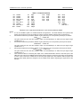
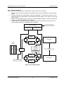
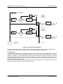
1
CMX7032
CMX7042
CML Microcircuits
AIS Data Processor
COMMUNICATION SEMICONDUCTORS
D/7032/42_FI1.1/2 September 2006
Provisional Issue
DATASHEET
Marine AIS data processor designed for Limiter-Discriminator based RF systems
Features:
• Half-Duplex GMSK and FSK Modem
• Low-Power (3.0 to 3.6V) Operation
• AIS and DSC Data Format
• Limiter-Discriminator Rx Interface
• Optimum Co-channel and Adjacent-channel
Performance
• Flexible Tx Interface: I and Q or
two-point modulation
• Flexible Channel Configuration:
– Two Simultaneous Rx
– One Tx
• Auxiliary ADC and DAC Functions
– 4 x (10-bit) DACs
– 2 x (10-bit) ADCs
• Supports Carrier-Sensing Channel Access
(CSTDMA) Operation
Applications:
• Low Profile 64 or 48 pad Leadless VQFN and
64 or 48 pin LQFP packages
• Automatic Identification System
(AIS) for Marine Safety
• Configurable by ‘Function Image’™
• AIS Aids To Navigation (AtoN)
• Two RF synthesizers (CMX7032 only)
• AIS Class B Transponders
• Two Auxiliary System Clock Generators
• AIS Rx-only or Tx-only Modules
Tx Section
Tx:
I/Q or
2-point
GMSK
Encoder
Output
Drivers
Message
Buffer
HDLC
NRZI
Encoder
C-BUS
Interface
Rx Section
GMSK
Decoder
Rx1:
LimiterDiscriminator
HDLC
NRZI
Decoder
FSK
Decoder
Rx2:
LimiterDiscriminator
GMSK
Decoder
Message
Buffer
Mesage
Buffer
HDLC
NRZI
Decoder
Mesage
Buffer
Sample
Timer
Interrupt
Generator
Reset and
Power
control
DACs
AIS
Radio
Tranceiver
ADCs
CMX7032
CMX7042
GPIO
Dual Clock Generators
Dual RF Synthesisers
(CMX7032 only)
© 2006 CML Microsystems Plc
Auxiliary
Section
Host
Micro
TCXO
AIS Baseband IC with / without RF Synthesizer
1
CMX7032/CMX7042
Brief Description
A highly integrated Baseband Signalling Processor IC, the CMX7032/CMX7042 fulfils the requirements of
the class B marine Automatic Identification System (AIS) transponder market.
The AIS system allows ships and base stations to communicate their position and other data to each
other without the need for a centralised controller. This allows vessels to “see” each other and take
appropriate action to avoid collision and so improve marine safety. The system uses a GMSK 9600 baud
data link in the Marine VHF radio band. The system requirements are defined in ITU-M 1371-1.
The CMX7032/CMX7042 is half duplex in operation, comprising two parallel Limiter-Discriminator Rx
paths and one I and Q or two-point modulation Tx path. The Rx paths are configurable for AIS or DSC
operation, the Tx for AIS only. The device performs signal modulation/demodulation with associated AIS
functions, such as training sequence detection, NRZI conversion and HDLC processing (flags, bit
stuffing/de-stuffing, CRC generate/check). Integrated Rx/Tx data buffers are also provided. This greatly
reduces the processing requirements of the host µC. Provision of a number of auxiliary ADCs and DACs
further simplifies the system hardware design, reducing the overall equipment cost and size.
The CMX7042 is identical in functionality to the CMX7032 with the exception that the two on-chip RF
Synthesizers have been deleted, which enables it to be supplied in a smaller package. This document
refers to both parts generically as the CMX7032, unless otherwise stated.
The CMX7032/CMX7042 devices utilise CML’s proprietary FirmASIC® component technology. On-chip
sub-systems are configured by a Function Image™: this is a data file that is uploaded during device
initialisation and defines the device's function and feature set. The Function Image™ can be loaded
automatically from an external EEPROM or from a host µController over the built-in C-BUS serial
interface. The device's functions and features can be enhanced by subsequent Function Image™
releases, facilitating in-the-field upgrades. This document refers specifically to the features provided by
Function Image™ 1.1.
This Datasheet is the first part of a two-part document comprising Datasheet and User Manual: the User
Manual can be obtained by registering your interest in this product with your local CML representative.
© 2006 CML Microsystems Plc
2
D/7032/42_FI1.1/2
AIS Baseband IC with / without RF Synthesizer
CMX7032/CMX7042
CONTENTS
1
Brief Description ............................................................................................................................... 2
2
Block Diagram ................................................................................................................................... 6
3
Signal List .......................................................................................................................................... 7
4
Recommended External Components .......................................................................................... 10
5
PCB Layout Guidelines and Power Supply Decoupling ............................................................. 13
6
General Description ........................................................................................................................ 15
6.1 Overview.................................................................................................................................. 15
6.2 AIS system formats ................................................................................................................. 16
7
Detailed Descriptions...................................................................................................................... 17
7.1 Clock Source ........................................................................................................................... 17
7.2 Host Interface .......................................................................................................................... 17
7.3 Function Image™ Load and Activation ................................................................................... 19
7.3.1
FI Loading from Host Controller .................................................................................. 19
7.3.2
FI Loading from EEPROM ........................................................................................... 20
7.4 System Description and Tasks................................................................................................ 21
7.4.1
Signal Routing.............................................................................................................. 21
7.4.2
Operating Modes ......................................................................................................... 21
7.4.3
Modem and Data Units ................................................................................................ 22
7.4.4
Timing and Synchronisation ........................................................................................ 22
7.4.5
Time of Arrival Reporting ............................................................................................. 22
7.4.6
Tx Timing ..................................................................................................................... 22
7.4.7
Rx Timing..................................................................................................................... 23
7.4.8
CSTDMA Threshold Measurement ............................................................................. 24
7.4.9
RSSI Measurement ..................................................................................................... 24
7.4.10 RSSI Calibration .......................................................................................................... 25
7.4.11 Auxiliary ADCs ............................................................................................................. 25
7.4.12 Auxiliary DACs ............................................................................................................. 25
7.4.13 Interrupt Operation....................................................................................................... 25
7.5 Operation of Tasks .................................................................................................................. 25
7.5.1
Tx Task Operation ....................................................................................................... 26
7.5.2
Rx Task Operation....................................................................................................... 27
7.5.3
Registers and Buffers for Tx/Rx Tasks........................................................................ 28
7.5.4
Write Data Registers.................................................................................................... 28
7.5.5
Read Data Registers ................................................................................................... 29
7.5.6
Data Tasks................................................................................................................... 29
7.5.7
Modem Tasks and Codes............................................................................................ 30
7.6 Transmission format ................................................................................................................ 30
7.6.1
Transmit Tasks ............................................................................................................ 31
7.6.2
AIS Burst Mode Transmit............................................................................................. 31
7.6.3
Transmit Example ........................................................................................................ 32
7.6.4
AIS Raw Mode Transmit.............................................................................................. 32
7.6.5
Transmitter Timing Control .......................................................................................... 32
7.6.6
Modulation Formats ..................................................................................................... 34
7.7 Reception ................................................................................................................................ 35
7.7.1
AIS Burst Mode Receive.............................................................................................. 35
7.7.2
AIS Raw Mode Receive............................................................................................... 36
7.7.3
DSC Receive ............................................................................................................... 37
© 2006 CML Microsystems Plc
3
D/7032/42_FI1.1/2
AIS Baseband IC with / without RF Synthesizer
CMX7032/CMX7042
7.7.4
Receive Example ......................................................................................................... 38
7.7.5
Rx Tasks ...................................................................................................................... 38
7.8 Configuration Tasks and Codes .............................................................................................. 39
7.9 RF Synthesizer (CMX7032 only)............................................................................................. 39
7.10 System Clock Synthesizers..................................................................................................... 42
7.11 Powersave ............................................................................................................................... 43
7.12 C-BUS Register Summary ...................................................................................................... 44
8
Performance Specification............................................................................................................. 45
8.1 Electrical Performance ............................................................................................................ 45
8.1.1
Absolute Maximum Ratings ......................................................................................... 45
8.1.2
Operating Limits........................................................................................................... 45
8.1.3
Operating Characteristics ............................................................................................ 46
8.1.4
Parametric Performance.............................................................................................. 50
8.2 C-BUS Timing.......................................................................................................................... 51
8.3 SPI Timing ............................................................................................................................... 52
TABLES
Table 1 Component Values ....................................................................................................................... 12
Table 2 BOOTEN pin states ...................................................................................................................... 19
Table 3 Data Tasks .................................................................................................................................... 29
Table 4 Modem Tasks ............................................................................................................................... 30
Table 5 AIS Burst Transmit Example......................................................................................................... 32
Table 6 Tx Sequence events ..................................................................................................................... 33
Table 7 Example Tx Event Sequence Setup ............................................................................................. 34
Table 8 Tx spectrum masks........................................................................................................................ 35
Table 9 AIS Burst Receive Example.......................................................................................................... 38
Table 10 Configuration Tasks .................................................................................................................... 39
Table 11 C-BUS registers .......................................................................................................................... 44
FIGURES
Figure 1 CMX7032 / CMX7042 Block Diagram ........................................................................................... 6
Figure 2 CMX7032 Recommended External Components ....................................................................... 10
Figure 3 CMX7042 Recommended External Components ....................................................................... 11
Figure 4 CMX7032 Power Supply Connections and De-coupling............................................................. 13
Figure 5 CMX7042 Power Supply Connections and De-coupling............................................................. 14
Figure 6 C-BUS Transactions .................................................................................................................... 18
Figure 7 FI Loading from Host ................................................................................................................... 20
Figure 8 FI Loading from EEPROM ........................................................................................................... 21
Figure 9 Tx Burst Timing............................................................................................................................ 23
Figure 10 Rx Burst Timing ......................................................................................................................... 24
Figure 11 Tx Task Operation ..................................................................................................................... 26
Figure 12 Rx Task Operation..................................................................................................................... 27
Figure 13 Typical AIS Transmission .......................................................................................................... 33
© 2006 CML Microsystems Plc
4
D/7032/42_FI1.1/2
AIS Baseband IC with / without RF Synthesizer
Figure 14
Figure 15
Figure 16
Figure 17
Figure 18
Figure 19
Figure 20
Figure 21
Figure 22
CMX7032/CMX7042
Example RF Synthesizer Components...................................................................................... 39
Single RF Channel Block Diagram ............................................................................................ 40
System Clock Generation .......................................................................................................... 43
C-BUS Timing ............................................................................................................................ 51
SPI Interface Timing .................................................................................................................. 52
Mechanical outline for 64-pad VQFN package (Q1) ................................................................. 53
Mechanical outline for 64-pin LQFP (leaded) package (L9)...................................................... 53
Mechanical outline for 48-pad VQFN package (Q3) ................................................................. 54
Mechanical outline for 48-pin LQFP (leaded) package (L4)...................................................... 54
© 2006 CML Microsystems Plc
5
D/7032/42_FI1.1/2
AIS Baseband IC with / without RF Synthesizer
2
CMX7032/CMX7042
Block Diagram
Mod 1 O/P
Transmit functions
Tx GMSK
AIS
HDLC
encode
buffer
NRZI
encode
Mod 2 O/P
GMSK
encode
Receive functions
RX1 in
GMSK
decode
NRZI
decode
HDLC
decode
buffer
Rx1 GMSK
AIS
buffer
FSK- DSC
buffer
Rx2 GMSK
AIS
Input 1
VBias
FSK
decode
RX2 in
mux
GMSK
decode
NRZI
decode
HDLC
decode
Input 2
VBias
Spare
ADC
VBias
TxENA
GPIO
SlotCLK
DAC 1
Aux DAC 1
DAC 2
Aux DAC 2
DAC 3
Aux DAC 3
DAC 4
Auxiliary functions
General
purpose I/O
Auxiliary
system
clocks
System Clock 1
SYS CLK 1
System Clock 2
SYS CLK 2
Ramp profile
RAM
RF I/P 1
Auxiliary
DACs
Synthesiser
1
RF Synthesisers
(CMX7032 only)
Aux DAC 4
Out CP1
ISet 1
RF I/P 2
Synthesiser
2
Internal Signal
RSSI 1
RSSI 2
RFVdd
Auxiliary
multiplexed
ADCs
MUX
AuxADC 1
Out CP2
ISet 2
Aux ADC 1
Aux ADC 2
CPVdd
RFVss
AuxADC 2
RF Clk
System Control
Main
Clock
Digital
PLL
EPSO
Boot En2
DVdd
AVss
AVdd
VBias
DVss
Reg
Bias
VDec
EPCSN
Boot
Control
Crystal
oscillator
Registers
Power control
Internal systems
control
IRQ
C-BUS
Interface
Reply Data
CSN
CMD Data
Serial Clk
XtalN
EEPROM
SPI port
Boot En1
EPSClk
Clk/Xtal
EPSI
Figure 1 CMX7032 / CMX7042 Block Diagram
© 2006 CML Microsystems Plc
6
D/7032/42_FI1.1/2
AIS Baseband IC with / without RF Synthesizer
3
CMX7032/CMX7042
Signal List
CMX7032 CMX7042
64-pin
48-pin
Q1 / L9
Q3 / L4
Signal
Name
Type
Description
1
8
IRQN
OP
C-BUS: A 'wire-ORable' output for connection to the Interrupt
Request input of the host. Pulled down to VSS(D) when
active and is high impedance when inactive. An external
pull-up resistor (R1) is required.
2
-
RF1 –
IP
RF Synthesizer #1 Negative Input.
3
-
RF1 +
IP
RF Synthesizer #1 Positive Input.
4
-
RFVss
PWR
5
-
CP1OUT
OP
1st Charge Pump output.
6
-
ISET1
IP
1st Charge Pump Current Set input.
7
-
RFVdd
PWR
8
-
RF2 –
IP
RF Synthesizer #2 Negative Input.
9
-
RF2 +
IP
RF Synthesizer #2 Positive Input.
10
-
RFVss
PWR
11
-
CP2OUT
OP
2nd Charge Pump output.
12
-
ISET2
IP
2nd Charge Pump Current Set input.
13
-
CHARGE PUMP
PWR
14
-
RF CLOCK
IP
RF Clock Input (common to both synthesizers)1.
15
-
-
NC
Reserved – do not connect this pin.
16
-
-
NC
Reserved – do not connect this pin.
17
-
-
NC
Reserved – do not connect this pin.
The negative supply rail (ground) for the RF synthesizers.
The 2.5V positive supply rail for the RF synthesizers. This
should be decoupled to RFVss by a capacitor mounted close
to the device pins.
The negative supply rail (ground) for the 2nd RF synthesizer.
The 3.3V positive supply rail for the RF charge pumps. This
should be decoupled to RFVss by a capacitor mounted close
to the device pins.
Internally generated 2.5V digital supply voltage. Must be
decoupled to DVss by capacitors mounted close to the
device pins. No other connections allowed, except for
optional connection to RFVdd.
18
9
VDEC
PWR
19
10
SLOT CLK
IP
Slot Clock from host (37.5Hz)
-
11
-
NC
Reserved – do not connect this pin.
-
12
-
NC
Reserved – do not connect this pin.
20
13
SYS CLK 1
OP
Synthesized Digital System Clock Output 1.
21
14
DVss
PWR
22
-
-
NC
Reserved – do not connect this pin.
23
15
TxEnable
OP
Enable for external Tx hardware
Digital Ground.
1
To minimise crosstalk, this signal should be connected to the same clock source as XTAL / CLOCK
input. By default, this is connected internally at power-on, alternatively, this may be achieved by
connecting the pin to the XTALN output when a 19.2MHz source is in use.
© 2006 CML Microsystems Plc
7
D/7032/42_FI1.1/2
AIS Baseband IC with / without RF Synthesizer
CMX7032 CMX7042
64-pin
48-pin
Q1 / L9
Q3 / L4
CMX7032/CMX7042
Signal
Name
Type
Description
24
16
Rx1IN
IP
Rx1 inverting input.
25
17
Rx1FB
OP
Rx1 input amplifier feedback.
26
18
Rx2IN
IP
Rx2 inverting input.
27
19
Rx2FB
OP
Rx2 input amplifier feedback.
28
20
SpareADCFB
OP
Spare ADC input amplifier feedback
29
21
SpareADCIN
IP
Spare ADC inverting input
30
22
AVss
PWR
31
23
MOD1
OP
Modulator 1 output.
32
24
MOD2
OP
Modulator 2 output.
Analog Ground.
33
25
VBIAS
OP
Internally generated bias voltage of about AVdd/2, except
when the device is in ‘Powersave’ mode when VBIAS will
discharge to AVss. Must be decoupled to AVss by a
capacitor mounted close to the device pins. No other
connections allowed.
34
26
-
NC
Reserved – do not connect this pin.
35
27
RSSI1
IP
Analog RSSI input from Limiter / Discriminator 1.
36
28
RSSI2
IP
Analog RSSI input from Limiter / Discriminator 2.
37
29
AUXADC1
IP
Auxiliary ADC input 1.
38
30
AUXADC2
IP
Auxiliary ADC input 2.
Analog +3.3V supply rail. Levels and thresholds within the
device are proportional to this voltage. This pin should be
decoupled to AVss by capacitors mounted close to the
device pins.
39
31
AVdd
PWR
40
32
AUXDAC1
OP
Auxiliary DAC output 1 / RAMDAC.
41
33
AUXDAC2
OP
Auxiliary DAC output 2.
42
34
AVss
PWR
43
35
AUXDAC3
OP
Auxiliary DAC output 3.
44
36
AUXDAC4
OP
Auxiliary DAC output 4.
-
37
DVss
PWR
Digital Ground.
Analog Ground.
45
38
VDEC
PWR
Internally generated 2.5V supply voltage. Must be decoupled
to DVss by capacitors mounted close to the device pins. No
other connections allowed, except for the optional connection
to RFVdd.
46
39
XTAL / CLOCK
IP
19.2MHz input from the external clock source or 9.6MHz Xtal
47
40
XTALN
OP
The output of the on-chip 9.6MHz Xtal oscillator inverter. NC
if 19.2MHz Clock used.
48
41
DVdd
PWR
49
42
COMMAND DATA
IP
© 2006 CML Microsystems Plc
Digital +3.3V supply rail. This pin should be decoupled to
DVss by capacitors mounted close to the device pins.
C-BUS: Serial data input from the µC.
8
D/7032/42_FI1.1/2
AIS Baseband IC with / without RF Synthesizer
CMX7032 CMX7042
64-pin
48-pin
Q1 / L9
Q3 / L4
CMX7032/CMX7042
Signal
Name
Type
Description
C-BUS: A 3-state C-BUS serial data output to the µC. This
output is high impedance when not sending data to the µC.
50
43
REPLY DATA
TS OP
51
44
-
NC
52
45
DVss
PWR
53
-
-
NC
Reserved – do not connect this pin.
54
46
SERIAL CLOCK
IP
C-BUS: The C-BUS serial clock input from the µC.
55
47
SYS CLK 2
OP
Synthesized Digital System Clock Output 2.
56
48
CSN
IP
C-BUS: The C-BUS chip select input from the µC
57
-
-
NC
Reserved – do not connect this pin.
58
1
EPSI
OP
EEPROM Serial Interface: SPI bus Output.
59
2
EPSCLK
OP
EEPROM Serial Interface: SPI bus Clock.
60
3
EPSO
61
4
EPSCSN
OP
62
5
BOOTEN1
IP+PD
Used in conjunction with BOOTEN2 to determine the
operation of the bootstrap program.
63
6
BOOTEN2
IP+PD
Used in conjunction with BOOTEN1 to determine the
operation of the bootstrap program.
64
7
DVss
PWR
Digital Ground.
Reserved – do not connect this pin.
Digital Ground.
IP+PD EEPROM Serial Interface: SPI bus Input.
EEPROM Serial Interface: SPI bus Chip Select.
Notes: Exposed metal pad on the bottom of a VQFN package should not be connected.
IP
=
Input (+PU/PD = internal pullup/pulldown resistor)
OP
=
Output
TS OP
=
3-state Output
PWR
=
Power Supply Connection
NC
=
No Connection
Functions with no associated pin number are not available in the CMX7042.
© 2006 CML Microsystems Plc
9
D/7032/42_FI1.1/2
AIS Baseband IC with / without RF Synthesizer
4
CMX7032/CMX7042
Recommended External Components
Figure 2 CMX7032 Recommended External Components
© 2006 CML Microsystems Plc
10
D/7032/42_FI1.1/2
AIS Baseband IC with / without RF Synthesizer
CMX7032/CMX7042
Figure 3 CMX7042 Recommended External Components
© 2006 CML Microsystems Plc
11
D/7032/42_FI1.1/2
AIS Baseband IC with / without RF Synthesizer
CMX7032/CMX7042
Table 1 Component Values
R1
R3
R4
R5
R6
R7
R8
R9
R10
100kΩ
100kΩ
100kΩ
See note 2
100kΩ
See note 3
100kΩ
See note 4
100kΩ
C1
C2
C3
C4
C7
C8
C9
C12
C14
18pF
18pF
10nF
10µF
100nF
100pF
100pF
100pF
100pF
C16
C17
C18
C19
C20
100pF
10µF
10nF
10nF
10µF
C21
C22
C23
C24
C25
C26
X1
10nF
10nF
10µF
10nF
10nF
10µF
9.6MHz
See note 1
Resistors ±5%, capacitors and inductors ±20% unless otherwise stated.
Notes:
1.
2.
3.
4.
5.
X1 can be a 9.6MHz crystal or a 19.2MHz external clock generator. The tracks between the crystal and the
device pins should be as short as possible to achieve maximum stability and best start up performance.
R5 should be selected to provide the desired dc gain (assuming C11 is not present) of the input, as follows:
⏐GAINRxIN1⏐ = 100kΩ / R5
The gain should be such that the resultant output at the RxIN1FB pin is within the input signal range
specified in 8.1.3.
R7 should be selected to provide the desired dc gain (assuming C13 is not present) of the input as follows:
⏐GAINRxIN2⏐ = 100kΩ / R7
The gain should be such that the resultant output at the RxIN2FB pin is within the input signal range
specified in 8.1.3.
R9 should be selected to provide the desired dc gain (assuming C15 is not present) of the input as follows:
⏐GAINSpareADC⏐ = 100kΩ / R9
The gain should be such that the resultant output at the RxIN2FB pin is within the input signal range
specified in 8.1.3.
Care should be taken in connecting the output of the Limiter-Discriminator device to the RxIN pins of the
CMX7032. The format of the GMSK signal requires that the frequency response of the input circuits extends
to below 10Hz, however the variations in the incoming AIS signals from many different stations require that
the input must rapidly follow the changes in DC and signal levels without de-grading the signal seen at the
RxIN pin.
© 2006 CML Microsystems Plc
12
D/7032/42_FI1.1/2
AIS Baseband IC with / without RF Synthesizer
5
CMX7032/CMX7042
PCB Layout Guidelines and Power Supply Decoupling
Figure 4 CMX7032 Power Supply Connections and De-coupling
Component Values as per Table 1.
© 2006 CML Microsystems Plc
13
D/7032/42_FI1.1/2
AIS Baseband IC with / without RF Synthesizer
CMX7032/CMX7042
Figure 5 CMX7042 Power Supply Connections and De-coupling
Component Values as per Table 1.
Notes:
1.
It is important to protect the analog pins from extraneous inband noise and to minimise the impedance
between the CMX7032 and the supply and bias de-coupling capacitors. The supply decoupling capacitors
should be as close as possible to the CMX7032. It is therefore recommended that the printed circuit board is
laid out with separate ground planes for the AVSS, RFVSS and DVSS supplies in the area of the CMX7032,
with provision to make links between them, close to the CMX7032. Use of a multi-layer printed circuit board
will facilitate the provision of ground planes on separate layers.
2.
It is recommended that no connection be made to the central metal pad on Q1,Q3 (VQFN) packages.
3.
VBIAS is used as an internal reference for detecting and generating the various analog signals. It must be
carefully decoupled to ensure its integrity so, apart from the decoupling capacitor shown, no other loads
should be connected. If VBIAS needs to be used to set the discriminator mid-point reference, it must be
buffered with an external high input impedance buffer.
4.
The 2.5V VDEC output can be used to supply the 2.5V RFVDD, to remove the need for an external 2.5V
regulated supply. VDEC can be directly connected to RFVDD.
© 2006 CML Microsystems Plc
14
D/7032/42_FI1.1/2
AIS Baseband IC with / without RF Synthesizer
6
CMX7032/CMX7042
General Description
6.1 Overview
Tx Modem Functions
• AIS 25kHz channel (GMSK, 9600bps, 2.4kHz deviation, BT=0.4)
• AIS Burst mode with full AIS frame formatting (HDLC-type)
o Bit stuffing
o NRZI coding
o Training sequence and start/stop flag insertion
o CRC generation
• AIS Raw mode (for greater flexibility)
o Supports arbitrary data streams for user-defined protocols
• Full support for the AIS Class B carrier-sensing channel access scheme (CS-TDMA)
• Full support for the AIS Class B Self-organising TDMA access scheme
• 160 byte (equivalent to 5 AIS slots) Tx data buffer
• Flexible Tx Interface
o Two-point modulation outputs, with independent gain and polarity controls
o I and Q modulation outputs, for use with an I/Q upconverter
Rx Modem Functions
• Configurable modulation format:
o AIS 25kHz channel (GMSK, 9600bps, 2.4kHz deviation, BT=0.4)
o DSC (de-emphasised FSK, 1200bps)
• Simultaneous reception of two AIS channels, or one AIS and one DSC channel
• AIS Burst mode with full AIS frame formatting (HDLC-type)
o Frame sync recognition
o Bit de-stuffing
o NRZI decoding
o Training sequence and start/stop flag detection
o CRC checking
• AIS Raw mode (for greater flexibility)
o Supports arbitrary data streams for user-defined protocols
• DSC reception supported in raw mode
• Four 160 byte Rx data buffers can automatically store up to four 5-slot AIS bursts (2 per Rx
channel)
• Rx signal input gain and polarity controls
• Time-of-arrival reporting assists with timekeeping in the absence of GPS
100 - 600 MHz RF Synthesizers (CMX7032 only)
• Two Integer-N synthesizers
• Flexible design minimizes reference spurs for low phase noise results
• Charge pump
o High/low soft selectable current setting to speed large frequency channel changes
o Nominal current user defined by external resistor value
• Lock detect
© 2006 CML Microsystems Plc
15
D/7032/42_FI1.1/2
AIS Baseband IC with / without RF Synthesizer
CMX7032/CMX7042
Analog I/O Functions
• Auxiliary ADC system
o Two 10-bit successive approximation ADCs with integrated sample and hold.
o One AuxADC is dedicated to RSSI measurement in a user defined window, the other is
available for general use.
• Ramping auxiliary DAC
o DAC sequences through a user-configured sequence of DAC output values to develop a
specific rising/falling DAC output signal. This is useful for ramping an RF PA, and can be
configured to happen automatically at the start and end of a burst.
o Can operate as a general purpose DAC, if desired.
• Three general purpose auxiliary DACs
System Functions
• All internal subsystems are controlled via a single serial host interface to reduce host µC pin
count and simplify external host driver complexity.
• Transaction oriented command/response logical host interface executes tasks supporting normal
operation, device configuration, and functions to assist manufacturing calibration trimming of
external circuits.
• Internal system clock derived from RF synthesizer reference oscillator and eliminates the need for
additional XTAL or baseband clock oscillator.
• User clock synthesizers generate two clocks for external use and eliminates an external clock
synthesizer when needed to support peripheral devices.
• User selected method for loading a Function Image™ - either from the host µC via C-BUS or
from an external serial EEPROM.
• Integrated 2.5V regulator can develop 2.5V from required 3.3V supply.
• Powersave facilities minimize total system power.
6.2 AIS system formats
The AIS system uses two basic channel access mechanisms – Self Organising Time Division Multiple
Access (SOTDMA) and Carrier-Sensing Time Division Multiple Access (CSTDMA). The CMX7032 is
compatible with both systems and offers additional features which simplify the implementation of
CSTDMA. The SOTDMA system is detailed in ITU-M 1371-1 and IEC 61993-2 while the CSTDMA is
detailed in IEC 62287.
The CSTDMA system is used in the implementation of the Class B-CS AIS. This requires the Receiver to
monitor the first part of a slot for an existing AIS transmission from another station before deciding to use
the slot for its own transmission or aborting and selecting a different slot.
The SOTDMA system is used in the Class A and Base Station AIS as well as the Class B-SOTDMA AIS
standard. The relevant International standards are:
[0]
ITU-M 1371-1
[1]
IEC 61993-2 Class A
[2]
IEC 62287-1 Class B CSTDMA
[3]
IEC 62287-2 Class B SOTDMA
[4]
IEC 62320-1 Base Station
[5]
IEC 62320-2 Aids to Navigation
© 2006 CML Microsystems Plc
16
D/7032/42_FI1.1/2
AIS Baseband IC with / without RF Synthesizer
7
CMX7032/CMX7042
Detailed Descriptions
7.1 Clock Source
The CMX7032 can be used with either a 9.6MHz xtal or a 19.2MHz oscillator. The RFCLOCK should also
be derived from this source to avoid the generation of unwanted spurious signals.
7.2 Host Interface
This section provides a general description of the C-BUS serial interface protocol used to transfer data,
control and status information between the CMX7032 and its host.
C-BUS is a serial interface, similar to SPI, that uses a simple transaction-oriented command/response
protocol with addressing to access specific registers within the CMX7032. Each C-BUS transaction
consists of a single Register Address/Command byte (A/C byte) sent from the µC which may be followed
by one or more data byte(s) sent from the µC to be written into one of the CMX7032’s Write Only
Registers, or one or more data byte(s) read out from one of the CMX7032’s Read Only Registers, as
illustrated in Figure 6.
Data sent from the µC on the Command Data line is clocked into the CMX7032 on the rising edge of the
Serial Clock input. Reply Data sent from the CMX7032 to the µC is valid when the Serial Clock is high.
The CSN line must be held low during a data transfer and kept high between transfers. The C-BUS
interface is compatible with most common µC serial interfaces and may also be easily implemented with
general purpose µC I/O pins controlled by a simple software routine.
The number of data bytes following an A/C byte is dependent on the value of the A/C byte. The most
significant bit of the address or data is sent first. For detailed timings see section 8.2.
© 2006 CML Microsystems Plc
17
D/7032/42_FI1.1/2
AIS Baseband IC with / without RF Synthesizer
CMX7032/CMX7042
C-BUS Write:
See Note 1
See Note 2
CSN
SerialCLK
Cmd_data
7
6
5
4
3
2
1
MSB
0
7
LSB
MSB
Address / Command byte
6
…
0
7
LSB
MSB
Upper 8 bits
…
0
LSB
Lower 8 bits
Reply_data
High Z state
C-BUS Read:
See Note 2
CSN
SerialCLK
Cmd_data
7
6
5
4
3
2
MSB
1
0
LSB
Address byte
Upper 8 bits
Reply_data
7
High Z state
Data value unimportant
6
MSB
Repeated cycles
…
Lower 8 bits
0
7
LSB
MSB
…
0
LSB
Either logic level valid
Figure 6 C-BUS Transactions
Notes:
1.
2.
3.
4.
5.
For Command byte transfers only the first 8 bits are transferred.
For single byte data transfers only the first 8 bits of the data are transferred.
The Cmd_data and Reply_data lines are never active at the same time. The Address byte determines the
data direction for each C-BUS transfer.
The SerialCLK input can be high or low at the start and end of each C-BUS transaction.
The gaps shown between each byte on the Cmd_data and Reply_data lines in the above diagram are
optional, the host may insert gaps or concatenate the data as required.
© 2006 CML Microsystems Plc
18
D/7032/42_FI1.1/2
AIS Baseband IC with / without RF Synthesizer
CMX7032/CMX7042
7.3 Function Image™ Load and Activation
The Function Image™ (FI), which defines the operational capabilities of the device, may be obtained from
the CML Technical Portal, following product registration. This is in the form of a 'C' header file which can
be included into the host controller software or programmed into an external EEPROM. The maximum
possible size of Function ImageTM is 46 kbytes, although a typical FI will be less than this. Note that the
BOOTEN pins are only read at power-on or following a C-BUS General Reset and must remain stable
throughout the FI loading process. Once the FI load has completed, the BOOTEN pins are ignored by the
CMX7032 until the next power-up or C-BUS General Reset.
The BOOTEN pins are both fitted with internal 100k (approx.) pull down resistors.
For C-BUS load operation, both pins should be pulled high by connecting them to Vdd either directly or via
a 4k7 resistor (see Table 2).
For EEPROM load, only BOOTEN1 needs to be pulled high in a similar manner, however, if it is required
to program the EEPROM in-situ from the host, either a jumper to Vdd or a link to a host I/O pin should be
provided to pull BOOTEN2 high when required (see Table 2).
Once the FI has been loaded, the CMX7032 performs these actions:(1)
(2)
(3)
(4)
(5)
the product identification code ($7032 or $7042) is reported in C-BUS register $C5
the FI version code is reported in C-BUS register $C9
the two 32-bit FI checksums are reported in C-BUS register pairs $A9, $AA and $B8, $B9
the device waits for the host to load the 32-bit Device Activation Code to C-BUS register $C8
once activated, the device initialises fully, enters idle mode and becomes ready for use.
The checksums can be verified against the published values to ensure that the FI has loaded correctly.
Once the FI has been activated, the checksum, product identification and version code registers are
cleared and these values are no longer available. If an invalid activation code is loaded, the device will
report the value $DEAD in register $A9 and become unresponsive to all further host commands (including
General Reset).
Both the Device Activation Code and the checksum values are available from the CML website.
Table 2 BOOTEN pin states
C-BUS Host load
reserved
EEPROM load
No FI load
Note:
BOOTEN2
1
1
0
0
BOOTEN1
1
0
1
0
In the rare event that a General Reset needs to be issued without the requirement to re-load the FI, the
BOOTEN pins must both be cleared to '0' before issuing the Reset command. The Checksum values will
be reported and the Device Activation code will need to be sent in a similar manner as that shown in
Figure 8. There will not be any FI loading delay. This assumes that a valid FI has been previously loaded
and that Vdd has been maintained throughout the reset to preserve the data.
7.3.1 FI Loading from Host Controller
The FI can be included into the host controller software build and downloaded into the CMX7032 at
power-up over the C-BUS interface. The BOOTEN pins must be set to the C-BUS load configuration, the
CMX7032 powered up and placed into Program Mode, the data can then be sent directly over the C-BUS
to the CMX7032.
Each time the device is powered up its Function Image™ must first be loaded and then activated. These
two steps assign internal device resources and determine all device features. The device does not
operate until the function image is loaded and activated.
© 2006 CML Microsystems Plc
19
D/7032/42_FI1.1/2
AIS Baseband IC with / without RF Synthesizer
CMX7032/CMX7042
BOOTEN2=1
BOOTEN1=1
Power-up / Reset CMX7032
Send Start Block 1 Address (DB1_ptr) to C-BUS $B6
Send Block 1Length (DB1_len) to C-BUS $B7
Wait for C-BUS $C6 bit 0 to be set to 1
Send $0001 to C-BUS $C8
Wait for C-BUS $C6 bit 0 to be set to 1
Send next data to C-BUS $C8
Send Start Block 2 Address (DB2_ptr) to C-BUS $B6
Send Block 2 Length (DB2_len) to C-BUS $B7
Wait for C-BUS $C6 bit 0 to be set to 1
Send $0001 to C-BUS $C8
Wait for C-BUS $C6 bit 0 to be set to 1
Send next data to C-BUS $C8
Send Start Block 3 Address (ACTIVATE_ptr) to C-BUS $B6
Send Block 3 Length (ACTIVATE_len) to C-BUS $B7
Wait for C-BUS $C6 bit 0 to be set to 1
Send $0001 to C-BUS $C8
Wait for C-BUS $C6 bit 0 to be set to 1
Verify Checksum values in $A9, $AA and
$B8, $B9
Send Device Activation Code hi to $C8
note: BOOTEN1 and
BOOTEN2 may be changed
at this point, if required
Wait for C-BUS $C6 bit 0 to be set to 1
Vdd
Send Device Activation Code lo to $C8
Wait for C-BUS $C6 bit 0 to be set to 1
BOOTEN1
CMX7032 is now ready for use
BOOTEN2
Figure 7 FI Loading from Host
The download time is limited by the clock frequency of the C-BUS, with a 5MHz SCLK, it should take less
than 500ms to complete.
7.3.2 FI Loading from EEPROM
The FI must be converted into a format for the EEPROM programmer (normally Intel Hex) and loaded into
the EEPROM either by the host or an external programmer. The CMX7032 needs to have the BOOTEN
pins set to EEPROM load, and then on power-on, or following a C-BUS General Reset, the CMX7032 will
automatically load the data from the EEPROM without intervention from the host controller.
© 2006 CML Microsystems Plc
20
D/7032/42_FI1.1/2
AIS Baseband IC with / without RF Synthesizer
CMX7032/CMX7042
BOOTEN2=0
BOOTEN1=1
Power-up / Reset CMX7032
Wait for C-BUS $C6 bit 0 to be set to 1
Verify Checksum values in $A9, $AA and
$B8, $B9
Send Device Activation Code hi to $C8
note: BOOTEN1 and
BOOTEN2 may be changed
at this point, if required
Wait for C-BUS $C6 bit 0 to be set to 1
Vdd
Send Device Activation Code lo to $C8
Wait for C-BUS $C6 bit 0 to be set to 1
BOOTEN1
CMX7032 is now ready for use
BOOTEN2
Jumper for
programming
EEPROM
(if required)
Figure 8 FI Loading from EEPROM
The CMX7032 has been designed to function with Atmel AT25HP512 EEPROM devices, however other
manufacturers parts may also be suitable. The time taken to load the FI is dependant on the clock / Xtal
source frequency, but should be less than 500ms.
7.4 System Description and Tasks
This section describes the operation of main sections of the CMX7032 and the task-oriented logical
interface provided to the external host device.
7.4.1 Signal Routing
The CMX7032 provides processing capability for two simultaneous receive channels (either two AIS or
one AIS and one DSC) or one Tx channel (AIS).
The inputs to the two receiver channels are nominally allocated to the Rx1IN and Rx2IN pins of the
device, however they can be re-allocated by the user by use of the Input Signal Routing C-BUS register,
$B1. The SpareADCIN pin can also be used as an input to the receivers if required. By default the device
will route Rx1IN to Rx channel 1 and Rx2IN to Rx channel 2, which leaves the SpareADCIN signal
available to the AuxADC. All of these inputs are configured around an inverting op-amp stage to facilitate
gain and filtering adjustments. In addition, the Rx channel inputs are equipped with programmable gain
stages for further level adjustments as required.
The Tx Modulation output signals may be configured to be suitable for two-point modulation circuits or
alternatively an I / Q upconverter. Signal levels on both output pins, MOD1 and MOD2 can be set to within
0.2dB using a Configuration Mode task.
7.4.2 Operating Modes
The CMX7032 operates in either:
o
Configuration mode.
o
Normal mode.
Configuration mode is used to set up various operating parameters of the CMX7032 subsystems e.g.
Transmit format, timing parameters etc. following a power-up or reset. The modem section is disabled
when the device is in Configuration mode. Configuration mode uses dedicated tasks that are not valid
whilst in Normal mode.
Normal mode is used when actively running the CMX7032 modem and other subsystems. Normal mode
uses dedicated tasks that are not valid whilst in Configuration mode.
© 2006 CML Microsystems Plc
21
D/7032/42_FI1.1/2
AIS Baseband IC with / without RF Synthesizer
CMX7032/CMX7042
“Enter config mode” (ECM) is a Normal mode task that switches the device from Normal to Configuration
mode. “Exit config mode” (EXIT_CONFIG) is a Configuration mode task that switches the device from
Configuration to Normal mode.
7.4.3 Modem and Data Units
The CMX7032 is logically divided into two main units which can accept and perform tasks separately:
o
Modem Unit
o
Data Unit
The Modem Unit is primarily responsible for processing Tx data from the internal Tx data buffer and
presenting it on the MOD1 and MOD2 pins, and processing the Rx input signals to recover the Rx data
they represent and storing that data in the internal Rx data buffers.
The Data Unit is primarily responsible for transferring data between the internal data buffers or
subsystems and the C-BUS registers, from where they can be accessed by the host µC.
When the device is in Normal mode, the Command Register, $C8, is a 16 bit C-BUS write register that
contains task fields for both Data and Modem units. A task is invoked by writing its code into the Data
Task or Modem Task fields. A single C-BUS write transaction will change all Command Register fields.
Often, the host will only want to issue either a Data or Modem task, in which case it should ensure that the
other task field is set to all zeroes, corresponding to a null / idle task. Sometimes it is useful to issue Data
and Modem tasks simultaneously, in which case, the Data task will always be completed before the
Modem task is started.
Certain internal subsystems can be directly accessed and controlled via C-BUS transactions, without
issuing a specific task / command.
7.4.4 Timing and Synchronisation
An AIS transponder must keep track of both the current AIS slot number and the position within the slot.
This is principally to ensure that transmissions occur at the right time, and that hardware is correctly
switched between Rx and Tx, but is also useful for scheduling when to take RSSI measurements, when
receivers can be powered down and when they should wake up again.
In an AIS Class A transponder, the clock is synchronised with a 1Hz tick from a GPS unit. In a Class B
transponder the clock may be synchronised to the GPS tick, or may be synchronised to the reception time
of AIS bursts from a Class A transponder or Base Station. Note that the latter scheme requires
management by the host µC, which must determine which received bursts are qualified to be used as a
timing reference. Whichever of these methods is used by the transponder, the CMX7032 requires a
SlotCLK input from the host µC. This should be a pulse at least 50us long, whose rising edge is aligned to
the AIS SlotCLK. An edge is required at the start of every AIS slot, hence the frequency of this signal is
37.5Hz.
The CMX7032 has several features to assist the host µC with timing, which are detailed below. All of
these features are based on the SlotCLK signal, provided by the host to the CMX7032’s SlotCLK pin. All
timings are defined as a number of 24kHz “ticks” referenced to the rising edge of the SlotCLK signal.
7.4.5 Time of Arrival Reporting
When the CMX7032 has received a burst as the result of a RXB1/2 (receive burst) task, the time of arrival
is presented as one of the first four words of the Data Block. This will give the time, measured in 24kHz
ticks, between the rising edge of the last SlotCLK and the detection of the last bit of the start flag of the
burst (Tsync in ITU-M 1371-1).
7.4.6 Tx Timing
The CMX7032 can be configured to perform a sequence of events when a TXB or TDBS task (transmit
burst) is issued. The events are start and end of modulation, ramping the RAMDAC up and down,
asserting and releasing a digital output pin (intended as a Tx Enable) and CSTDMA sensing. Each of
© 2006 CML Microsystems Plc
22
D/7032/42_FI1.1/2
AIS Baseband IC with / without RF Synthesizer
CMX7032/CMX7042
these can be configured to happen with specified delays from the rising edge of the SlotCLK. The timings
are set up with the config mode task Tx_Sequence. See User Manual section 11.15.7 for details.
Tx Timing
slot clock
Tx Enable
slot clock
PA Ramp &
Modulation
Time
CS-TDMA
Wait
Sensing
Figure 9 Tx Burst Timing
If CSTDMA sensing has been enabled then the CMX7032 will measure the carrier level (RSSI) on the
selected channel during the window specified in the transmit timing table. If the user-specified threshold is
exceeded then the subsequent events (RAMDAC, Tx Enable and modulation) will be cancelled. The
threshold is set using the CS_Threshold register, $C2. See User Manual section 11.12 for details.
7.4.7 Rx Timing
The CMX7032 has a power-saving mode, where it spends most of its time ‘asleep’, but ‘wakes up’ at the
start of each AIS slot and receives for long enough to determine whether a burst is present or not. If no
burst is received the CMX7032 will make a pair of RSSI measurements and then go back to sleep. This
power saving operation can be turned on and off using the Sleep Mode En bit in the Mode register, $C1.
The CMX7032 will still respond to C-BUS accesses when ‘asleep’ but the latency between a task being
issued and completed may be longer than normal.
The times to perform RSSI measurements, go to sleep, and wake up are configured by the host, and all
times are referenced to the SlotCLK signal. The host should ensure that these timings result in the
CMX7032 being awake in time to sample the next SlotCLK signal. The timings are set up using the
Sleep_Timing Config task. See User Manual section 11.15.8 for details.
If Sleep mode is not enabled, then the demodulator will run continuously and update the Rx Data buffer
whenever valid data is received.
© 2006 CML Microsystems Plc
23
D/7032/42_FI1.1/2
AIS Baseband IC with / without RF Synthesizer
CMX7032/CMX7042
Rx Timing
slot clock
slot clock
Received Burst
Time
Wait
Training
sequence
search
RSSI
Measurement
Sleep (if no burst received)
Wake up in time for
next slotclock
Figure 10 Rx Burst Timing
7.4.8 CSTDMA Threshold Measurement
The CMX7032 provides support for the CSTDMA mode of operation by measuring the signal level at the
start of a slot period and aborting the transmission if a level over a user defined threshold is found. This
fact is reported to the host in Status2 C-BUS register $C5.
The CSTDMA threshold measurement window is setup by the Tx_Sequence Config task using timing
values based on the number of 24kHz “tick” increments from the rising edge of the SlotCLK pulse. During
this period (if Tx_Status and CS-ENA are both “active”) the CMX7032 will measure the RSSI level of the
appropriate channel (set in C-BUS Mode register $C1):
1.
2.
3.
4.
5.
6.
sample RSSI at 48k samples/sec
scale values to 0 -128
apply the look-up table values
apply the CSTDMA_gain value
accumulate values over the defined period
compare the value with the value in the C-BUS CS-Threshold register $C2 and abort the
transmission if it is exceeded.
Note that the same lookup table is used for both CSTDMA Threshold measurement as the RSSI
measurement.
7.4.9 RSSI Measurement
RSSI can not be determined directly from the baseband signal output of a limiter-discriminator device so
the CMX7032 has two dedicated inputs (one for each Rx channel) for separate external analogue RSSI
signals. Suitable outputs are available on many limiter-discriminator ICs, e.g. Philips SA605. The ADCs
sample the signals during a user-defined window and apply an averaging algorithm and present the
results in C-BUS registers $BA and $BB.
The RSSI measurement windows are set up using the RSSI_Window config task using timing values
based on the number of 24kHz “tick” increments from the rising edge of the SlotCLK plulse. During this
period (if Tx_Status is not “active”) the device will:
1.
2.
3.
4.
5.
6.
sample RSSI at 48k samples/sec
scale values to 0 -128
apply the look-up table values
apply the RSSI_gain value
accumulate values over the defined period
output values to C-BUS registers
© 2006 CML Microsystems Plc
24
D/7032/42_FI1.1/2
AIS Baseband IC with / without RF Synthesizer
CMX7032/CMX7042
Note that the RSSI measurements on each RF channel run consecutively and that the C-BUS registers
are updated at the end of the RSSI_2 measurement window.
7.4.10 RSSI Calibration
The RSSI signal should be approximately logarithmically scaled (i.e. a nearly linear relationship between
voltage and signal strength in dBs). In order to reduce the impact of noise, the CMX7032 averages over
several samples, but to give a meaningful average, the samples must first be anti-logged. In order to
correct any non-linearities in the RSSI response, and to set an offset for the anti-logging the host must
supply calibration data.
The calibration data is a 128-entry table. The entries correspond to equally-spaced voltages from 0V to
3.3V applied to the RSSI inputs. To set up the table the host uses the Setup_RSSI_Calibration config
task. See section 7.8 for details. The default values are shown in User Manual section 11.15.3.
7.4.11 Auxiliary ADCs
The first Auxiliary ADC is dedicated to RSSI measurements at times specified by the host uC, see Section
7.4.8 and User Manual 11.15.4. The second Auxiliary ADC is available for user functions. The ADC runs
continuously, the input selected by the AuxADC Input Select bits in the C-BUS Mode register, $C1 and
the results of the conversion are presented in AuxADC Data C-BUS register $C9. This register also
includes a bit field to indicate which input was selected when this conversion was executed. The AuxADC
input can be routed to either of the RxIN signals, the SpareADC Input, the RSSI inputs or the AuxADC
inputs under host control. In normal operation it is expected to be routed to one of the AuxADC Inputs.
7.4.12 Auxiliary DACs
The four Auxiliary DACs can be updated in any combination using the AuxDACWrite data task. In
addition, DAC1 can be configured as a RAMDAC to output a series of values as part of the transmit timing
sequence. The values and the rate at which they change are set up using config mode task.
7.4.13 Interrupt Operation
The CMX7032 will issue an interrupt on the IRQN line when the IRQ bit (bit 15) of the Status register and
the IRQ Mask bit (bit 15) are both set to ‘1’. User Manual section 11.17 describes the situations which
cause the IRQ bit to change from a ‘0’ to a ‘1’. The IRQN pin is an open collector output that requires an
external pull-up resistor.
7.5 Operation of Tasks
This section describes modem and data tasks. Understanding their operation requires knowledge of the
internal buffering of the CMX7032.
Tx and Rx data is double buffered. Each Tx or Rx channel has a Data Buffer. The host µC accesses the
C-BUS registers and the modulator/demodulator directly accesses the Data Buffers. Tasks transfer data
between the buffers and the C-BUS registers.
© 2006 CML Microsystems Plc
25
D/7032/42_FI1.1/2
AIS Baseband IC with / without RF Synthesizer
CMX7032/CMX7042
7.5.1 Tx Task Operation
Typical stages of Tx task operation are depicted in Figure 11 and occur as follows:
1. The host writes up to 4 words of data for transmission into the Write Data C-BUS registers.
2. The host writes the Command register, specifying a data task. This results in transfer of the data
from the Write Data registers into the Tx Data Buffer.
3. Steps 1 and 2 can be repeated to load the Tx Data Buffer with a large block of data.
4. A Modem task can then be used to instruct the Tx Modulate pump to transmit the data in the Data
Buffer. This causes the content of the Tx Data Buffer to be coded and CRC’d (if in burst mode)
and transmitted to the MOD1 and MOD2 output pins.
5. Once the system is up and running any modem task may potentially take some time to execute
as it may have to wait for the previous task to complete.
Command Register
Data Task
Command Reg Free
Modem Task
C-Bus
registers
B
7
B
6
A
8
A
7
Tx Data Buffer
(88 words)
Data Task Complete
modulator
TBFree
TxState
TxDone
Figure 11 Tx Task Operation
© 2006 CML Microsystems Plc
26
D/7032/42_FI1.1/2
AIS Baseband IC with / without RF Synthesizer
CMX7032/CMX7042
7.5.2 Rx Task Operation
Typical stages of Rx task operation are depicted in Figure 12 and occur as follows:
1. A Modem task instructs the CMX7032 to transfer data from the Rx1/2 Modem to the Rx1/2 Data
Buffer.
2. The host writes the Command register, specifying a Data task. This results in transfer of up to 4
words from the Rx1/2 Data Buffer into the Read Data C-BUS registers, from where it can be read
by the host µC.
3. Steps 2 can be repeated (with host µC reads of the Read Data registers) to transfer a large block
of data from the Rx1/2 Data Buffer to the host µC.
4. Once the system is up and running any modem task may take some time to execute, as it will
need to wait for the data to be available from the modem.
Command Register
Data Task
Command Reg Free
Modem Task
Rx Data
Buffer
(88 words)
sw
sw
demodulator
Rx Data
Buffer
(88 words)
C-Bus
registers
R1BRDY
R1OVF
B
9
B
8
A
A
A
9
select
R2OVF
RxState
R2BRDY
Rx Data
Buffer
(88 words)
sw
Data Task Complete
sw
demodulator
Rx Data
Buffer
(88 words)
Figure 12 Rx Task Operation
© 2006 CML Microsystems Plc
27
D/7032/42_FI1.1/2
AIS Baseband IC with / without RF Synthesizer
7.5.3
CMX7032/CMX7042
Registers and Buffers for Tx/Rx Tasks
•
Command register: contains Data and Modem task fields as described above.
•
Status register – contains bits that indicate when tasks are complete, which can interrupt the
host:
o Command Reg Free
o TBFREE
o R1BRDY
o R2BRDY
o TxDONE
o Rx1OVF
o Rx2OVF
o Config Task Complete
o Data Task Complete
•
Interrupt Mask: Host write register to specify which status bit can cause an interrupt.
•
Write Data registers 0-3: Contain data written from host µC to transmit via the Tx Modulator.
•
Read Data registers 0-3: Contain data received from Rx Demod for host µC to read.
•
Tx Data Buffer: The Tx Data is double buffered, which allows the host µC to write to the Tx Data
Buffer while the modulator is simultaneously transmitting data it reads from the Tx Modem Buffer.
Each buffer is capable of holding one full (5-slot) AIS message.
•
Rx1/2 Data Buffer: The demodulator writes data directly into these internal buffers. There are two
buffers per channel which are used alternately every time a new burst is detected. This allows the
host µC to read from one buffer while reception continues to fill the other. Each buffer is capable
of holding a full (5-slot) AIS message.
7.5.4 Write Data Registers
An array of four, 16 bit, C-BUS write registers form the Write Data C-BUS registers.
The device reads and acts upon the content of these data write registers as instructed by the Data Task
bits of the Command register while in transmit mode. Generally, they may be written at any time by the
host µC with no effect on internal device operation. When a “Data task” is issued the Data registers will
be read by the device and so should not be modified by the host µC until the Data Task complete bit is set
in the Status register.
Data tasks access the registers as a number of words (1 to 4) or as a number of bits (1 to 16 in $A7),
however if a bit-format Data Task is used it must be the final data task issued in a multi-data transfer from
the host. The next data task issued should be a DataWordReset or DataBitReset to re-initialise the
internal data buffer pointers (a bit-format task is usually used as the last transfer of a data block that is not
a complete number of words in length).
Word-format:
Bit:
Register $A7
Bit:
Register $A8
Bit:
Register $B6
Bit:
Register $B7
15
14
13
15
14
13
15
14
13
15
14
13
12
11
10
9
8
7
6
5
4
Data write from host µC to device word 1(MSB sent first)
12
11
10
9
8
7
6
5
4
Data write from host µC to device word 2(MSB sent first)
12
11
10
9
8
7
6
5
4
Data write from host µC to device word 3(MSB sent first)
12
11
10
9
8
7
6
5
4
Data write from host µC to device word 4(MSB sent first)
3
2
1
0
3
2
1
0
3
2
1
0
3
2
1
0
Bit-format:
Bit:
Register $A7
15
14
13
© 2006 CML Microsystems Plc
12
11
10
9
8
7
6
5
4
3
Data write from host µC to device bits 0-15, (bit 15 transmitted first)
28
2
1
0
D/7032/42_FI1.1/2
AIS Baseband IC with / without RF Synthesizer
CMX7032/CMX7042
7.5.5 Read Data Registers
An array of four, 16 bit, C-BUS read registers form the Read Data C-BUS registers.
The device writes into these registers as instructed by the Data Task bits of the Command register while
in receive mode. The host µC can read these registers at any time except while a data task is in
progress, in which case the host µC should wait until the Data task complete bit is set in the Status
register.
Data tasks access the registers as a number of words (1 to 4) or as a number of bits (1 to 16 in $A7),
however if a bit-format Data task is used it must be the final data task issued in a multi-data transfer to the
host. The next data task issued should be a DataWordReset or DataBitReset to re-initialise the internal
data buffer pointers (a bit-format task is usually used as the last transfer of a data block that is not a
complete number of words in length).
Word-format:
Bit:
Register $A9
Bit:
Register $AA
Bit:
Register $B8
Bit:
Register $B9
15
14
13
12
15
14
13
12
15
14
13
12
15
14
13
12
15
14
13
11
10
9
8
7
6
5
4
Data read from device to host µC word 1 (MSB Rx first)
11
10
9
8
7
6
5
4
Data read from device to host µC word 2 (MSB Rx first)
11
10
9
8
7
6
5
4
Data read from device to host µC word 3 (MSB Rx first)
11
10
9
8
7
6
5
4
Data read from device to host µC word 4 (MSB Rx first)
3
2
1
0
3
2
1
0
3
2
1
0
3
2
1
0
12
11
10
9
8
7
6
5
4
3
Data read from device to host µC bits 0-15, (bit 15 received first)
2
1
0
Bit-format:
Bit:
Register $A9
7.5.6 Data Tasks
Data tasks are used to:
• Load data from the Write Data registers into Data Buffers while in normal or configuration modes.
• Load data from Data Buffers into the Read Data registers while in normal mode.
• Read, write or operate subsystems by passing data using the Write Data and Read Data
registers.
Table 3 Data Tasks
Name
NULL
DataWordReadNRx1
DataWordReadNRx2
DataWordWriteNTx
DataWordResetNRx1
DataWordResetNRx2
DataWordResetNTx
DataBitReadNRx1
DataBitReadNRx2
DataBitWriteNTx
Description
Null system task – takes no action.
• Copy N words (1 to 4) from Rx1 data buffer to C-BUS Read Data registers.
• Increment Rx1 data buffer pointer.
• Copy N words (1 to 4) from Rx2 data buffer to C-BUS Read Data registers.
• Increment Rx2 data buffer pointer.
• Copy N words (1 to 4) from Write Data registers to Tx data buffer.
• Increment data buffer pointer.
• Reset Rx1 data buffer pointer to the top.
• Copy N words (1 to 4) from Rx1 data buffer to Read Data registers.
• Increment data buffer pointer.
• Reset Rx2 data buffer pointer.
• Copy N words (1 to 4) from Rx2 data buffer to Read Data registers.
• Increment data buffer pointer.
• Reset Tx data buffer pointer.
• Copy N words (1 to 4) from Write Data registers to Tx data buffer.
• Increment the data buffer pointer.
• Copy N bits (1 to 15) from Rx1 data buffer to Read Data register 0.
• Increment the data buffer pointer.
• Copy N bits (1 to 15) from Rx2 data buffer to Read Data register 0.
• Increment data buffer pointer.
• Copy N bits (1 to 15) from Write Data register 0 to Tx data buffer.
• Increment data buffer pointer.
© 2006 CML Microsystems Plc
29
D/7032/42_FI1.1/2
AIS Baseband IC with / without RF Synthesizer
DataBitResetNRx1
DataBitResetNRx2
DataBitResetNTx
AuxDACWrite
CMX7032/CMX7042
• Reset Rx1 data buffer pointer.
• Copy N bits (1 to 15) from Rx1 data buffer to Read Data register 0.
• Increment the data buffer pointer.
• Reset Rx2 data buffer pointer.
• Copy N bits (1 to 15) from Rx1 data buffer to Read Data register 0.
• Increment data buffer pointer.
• Reset Tx data buffer pointer.
• Copy N bits (1 to 15) from Write Data register 0 to Txdata buffer.
• Increment data buffer pointer.
Interprets each of the first 1 to 4 words in the Write Data registers as a write command for the Auxiliary
DACs
7.5.7 Modem Tasks and Codes
Modem tasks transmit data on the MOD1 and MOD2 output pins or receive and recover data from the
RxIN pins. Modem tasks also coordinate data transfer between the Data Buffers and their respective
Modems.
Note that for receive tasks a 1 or 2 at the end of the task name refers to the Rx channel which is being
addressed.
Table 4 Modem Tasks
Name
NULL
Abort1
Abort2
AbortTx
ECM
Rx Tasks
Rx Raw bit = 0
RXB1
RXB2
Description
No command – takes no action.
Abort the ongoing modem task on Rx1, Rx2 or Tx.
Enter Configuration mode.
Rx Raw bit = 1 or channel is set to DSC.
Rx Burst: Wait for a training sequence, then
demodulate, decode and store the burst.
RXR1
RXR2
Tx Tasks
Tx Raw bit = 0
TXB
Code and transmit AIS message using contents
of data buffer. Start on next slot clock.
Tx Raw bit = 1
TDBS
TDB
PRBS
TRW
HCT
Demodulate and store N words. N is
defined by Rx data count register.
Transmit contents of data buffer. Start on
next slot clock.
Transmit N data bits from the Tx mod
buffer. Start as soon as modulator is free.
Transmit pseudorandom bit sequence.
Repeatedly transmit one word.
Hardware Control
7.6 Transmission format
The CMX7032/CMX7042 is capable of transmitting AIS data in either raw mode or burst mode. AIS
Carrier Sensing (CSTDMA) for Class B systems is supported.
In AIS raw mode, data is passed directly from the Tx Data Buffer to the GMSK modulator, so the µC will
be responsible for sending any necessary training sequences and performing HDLC processing and NRZI
coding.
In AIS burst mode, the CMX7032/CMX7042 uses an internal message buffer to assemble an entire
message (up to 5 slots) to which it automatically adds the training sequence, start/stop flags, CRC, bit
stuffing and NRZI coding prior to transmission.
After setting up the appropriate registers, transmission is initiated by issuing a Tx Burst or Tx Raw task.
© 2006 CML Microsystems Plc
30
D/7032/42_FI1.1/2
AIS Baseband IC with / without RF Synthesizer
7.6.1
•
•
CMX7032/CMX7042
Transmit Tasks
AbortTx:
This causes the current task on the Tx channel to abort. It also clears the Tx modem buffer.
TXB – Transmit AIS Burst
This task can only be executed if the Tx Raw bit (bit 5 in the command register) is cleared to ‘0’.
This causes the CMX7032 to take the contents of the Tx Data buffer, apply AIS data coding and
transmit the resulting AIS message. The transmit sequence will start on the next SlotCLK edge.
The following four transmit tasks can only be executed if the Tx Raw bit is set to ‘1’
•
•
•
•
•
TDBS – Transmit Data Buffer on SlotCLK
This causes the CMX7032 to transmit the data buffer contents using AIS modulation. No data
coding is applied, the Transmit Sequence will start on the next SlotCLK edge.
TDB – Transmit Data Buffer
This causes the CMX7032 to transmit the data buffer contents using AIS modulation. No data
coding is applied. The data will be transmitted as the modulator is available (Transmit Sequence
is ignored).
PRBS – Transmit pseudorandom bit sequence
This task causes the CMX7032 to transmit an internally generated pseudorandom bit sequence.
The sequence is 511 bits in length, but will repeat indefinitely until aborted using the Abort Tx
task, (Transmit Sequence is ignored).
TRW – Transmit Repeated Word
This task causes the CMX7032 to repeatedly transmit the first word currently in the data buffer.
Transmission will start immediately and will continue until an Abort Tx task is issued, (Transmit
Sequence is ignored).
HCT – Hardware Control Task
Allows manual control of ancilliary hardware functions.
7.6.2 AIS Burst Mode Transmit
In AIS burst mode, the CMX7032/CMX7042 responds to a TXB task by performing bit stuffing, NRZI
encoding and the addition of training sequence, start/stop flags and CRC checksum as required by AIS.
Note: in AIS burst mode, the data words are automatically transmitted least significant bit first as required
by the AIS specification.
A number of error conditions are checked for during AIS burst mode transmit, each of which causes
transmission to be aborted and a Tx Done interrupt to be generated. The associated Tx States are:
•
•
•
Tx aborted, message too long:
This occurs if the internal message buffer is not big enough for the HDLC coded data (should not
happen in normal operation, as the message buffer is big enough for a 5-slot message). This
condition requires the µC to issue a AbortTx task.
Tx aborted, carrier sensed:
This occurs if the CSTDMA mechanism is enabled and the CS measurement has exceeded the CS
Threshold. The data is retained so that it can be re-transmitted in a subsequent slot (by issuing
another TXB task) should the host request it. The slot selection should follow the rules given in the
relevant international standard.
Tx aborted, buffer not ready:
This occurs in burst mode if the internal data coding has not completed before the timing_start value
expires.
© 2006 CML Microsystems Plc
31
D/7032/42_FI1.1/2
AIS Baseband IC with / without RF Synthesizer
CMX7032/CMX7042
7.6.3 Transmit Example
The following detailed example describes the process of loading and transmitting an AIS message in
Burst mode.
Table 5 AIS Burst Transmit Example
Description
1.
The host should ensure that the TBFREE, Data Task and CmdReg
Free bits are set.
2. The host loads the first N(typically 4) data words into the write data
registers.
3. The host issues a DataWordResetNTx Data Task.
4. Device reads the command register & notes task types
5. Device carries out the data task by copying the N data words as
the first N data words of the data buffer
6. The steps above may be repeated (Using DataWordWriteN tasks)
to load many words until the data buffer contains enough data to
carry out the desired modem task.
7. The host writes a TXB task to the command register to start the Tx
process.
8. Device reads the Command register
9. Device codes the data. Tx state changes from Idle to Tx Pending
10. When the transmit point arrives (SlotCLK), the Tx State changes to
Tx in progress and the TxSequence is activated.
11. The Tx Modem Buffer will gradually empty as the Tx Modulator
continues transmitting.
12. When the transmission ends the TxDone bit in the Status register
will be set, generating an interrupt if enabled. The host should then
check the Tx state bits in the Status2 register to see if
transmission was successful.
Cmd
Reg Free
1
Data
Task
1
TBFREE
TxDONE
1
1
1
1
1
1
0
1
1
1
0
1
1
1
1
1
1
1
0
1
1
1
1
1
1
1
0
1
1
0
1
1
1
1
1
1
1
1
Note that if CSTDMA mode is active and a carrier is sensed in the selected channel at the beginning of
the requested transmit slot, the transmission is aborted (Tx State changes to Tx aborted, carrier sensed)
– this causes a TxDone interrupt to be generated, however the data in the Tx Data Buffer is retained, so
the µC can choose to issue an AbortTx task and clear the Tx Data Buffer, or reschedule the transmission
in another slot.
7.6.4 AIS Raw Mode Transmit
In AIS raw mode, transmit data is passed directly from the Tx Data Buffer to the GMSK modulator. The
µC must calculate the entire transmitted message including the training sequence, HDLC processing
(start/stop flags, bit stuffing, and CRC insertion) and NRZI coding. Note: In AIS raw mode, data words
written to the CMX7032 are transmitted most significant bit first. The AIS message structure, however,
requires each message byte to be output least significant bit first. The µC must therefore ensure that
during the process of HDLC processing and NRZI coding that the resulting data bytes are correctly
reversed.
7.6.5 Transmitter Timing Control
The CMX7032/CMX7042 can be configured to control the timing of transmission events whenever a Tx
Burst Modem task is executed. This includes the enabling of external RF circuits (e.g. synthesisers and
power amplifier), as well as the time at which internal data modulation begins. The flexibility of this timing
control allows the CMX7032/CMX7042 to be simply adapted to the characteristics of the RF transmit
circuits. The control of the external RF transmit circuits is performed using the TxEnable pin and the
AuxDAC1 ramping function.
© 2006 CML Microsystems Plc
32
D/7032/42_FI1.1/2
AIS Baseband IC with / without RF Synthesizer
RF
power
CMX7032/CMX7042
SlotCLK
SlotCLK
modulation
100%
B
CS sense period
Time
Figure 13 Typical AIS Transmission
A typical AIS transmission is shown in Figure 13. The CMX7032/CMX7042 starts timing relative to the
rising edge of SlotCLK. At the end of a transmission, a sequence of “power-down” actions is performed
which are timed relative to the last message bit having been modulated, shown as point B in Figure 13. In
this way differences in message length due to bit stuffing are automatically accommodated.
The relative timings of the transmit sequence events are configured as a table of values that are loaded
into the CMX7032/CMX7042 using a Config Task operation (User Manual section 11.15.7) – this
operation must be performed before any transmissions are attempted. Typically, this will only need to be
done once as part of an initialisation routine. All timings are measured in units of “ticks”, each of which
lasts for 1/24000Hz ( ≅ 41.666µs).
The transmit sequence consists of two initial setting values followed by a number of different event types.
These are:
• Initial delay from the SlotCLK edge
• Active state of the TxEnable pin
• Changes to the external hardware, via the TxEnable pin (typically used to turn the Tx on/off) and
the AuxDAC1 ramp up/down.
• Trigger for the start/end of the CSTDMA sensing period (if CSTDMA is enabled).
• Timing triggers for the start and end of the data modulation.
• A dummy event in case any of the above are not required in the application.
The transmit event sequence is programmed using a Config task, see User Manual section 11.15.7.
b3
0
0
0
0
0
0
0
b2
0
0
0
0
1
1
1
b1
0
0
1
1
0
0
1
b0
0
1
0
1
0
1
0
Event id
dummy
CSTDMA_START
CSTDMA_END
Tx_ON
RAMDAC_UP
MODULATE_START
MODULATE_END
0
0
1
1
1
0
1
0
RAMDAC_DOWN
Tx_OFF
description
Do nothing
Defines the start of the CSTDMA sensing window
Defines the end of the CSTDMA sensing window
Pin TxEnable is asserted
AuxDAC1 will start executing a Ramp up
Defines the start of data modulation
Delay from the end of modulation (based on the last data bit loaded into
modem - includes a 20 tick delay for the internal filters)
AuxDAC1 will start executing a Ramp down
Pin TxEnable is de-asserted
Table 6 Tx Sequence events
When calculating the MODULATE_START timing value, the delay through the CMX7032/CMX7042’s
internal transmit filters and any external components must be taken into account to ensure that data bits
appear on-air at the correct time (the filter delays are specified in section 8.1.4.The MODULATE_END
event has an in-built delay of 20 ticks to allow the last bit to make its way out of the transmit filter.
Allowance must be made for this built-in delay, as well as for the delay through any external components,
when calculating the timing of the transmit power down events.
A working example of how to set up a transmit event sequence is shown in Table 7 (the order of events
and delay timings shown are for illustrative purposes only):
© 2006 CML Microsystems Plc
33
D/7032/42_FI1.1/2
AIS Baseband IC with / without RF Synthesizer
CMX7032/CMX7042
Parameter
event
delay
total
Explanation
CSTDMA_START
1
10
20
Insert 10 tick delay then start monitoring the chosen Rx
input for a signal which may cause an abort (if CSTDMA
enabled).
MODULATE_START
5
17
37
Insert 17 tick delay then start feeding data to the transmit
modulator and filters (this allows for the 20 tick storage
delay in the Tx filters so that modulated data appears at
the end of the RAMDAC ramp_up period – tick 57).
CSTDMA_END
2
10
47
Insert 10 tick delay then stop CSTDMA monitoring.
TX_ON
3
0
47
Assert the TxEnable line (assuming not aborted)
Insert 3 tick delay then initiate the RAMDAC ramp-up (for
AIS, the transmitted signal will be carrier only at this point)
At this point during a transmission the CMX7032/CMX7042 feeds the entire message to the transmit modulator bitby-bit. All subsequent transmit events are timed relative to the end of the last message bit, indicated by the
MODULATE_END event.
RAMDAC_UP
4
3
50
MODULATE_END
6
0
0
The 0 delay defines this reference point as the same as
the output of the final data bit to the RF circuits (“B” in
Figure 13).
RAMDAC_DOWN
7
0
0
Initiate the RAMDAC ramp-down immediately
TX_OFF
8
8
8
Insert 7 tick delay (to allow RAMDAC to fully ramp down)
then release the TxEnable line.
Notes:
1. It is essential that the CSTDMA, and MODULATE START events precede their associated END events,
otherwise undesirable results will be obtained.
2. MODULATE_START must appear in the first group of timed events (table entries 1–5), MODULATE_END must
appear in the final group (table entries 6-8).
3. It is feasible to place the RAMDAC_DOWN task before the MODULATE_END task if it is desired to continue
modulation during the Ramp down period.
Assuming that the timing_start value has been set to 10 (see User Manual section 11.15.7) and the RAMDAC is set
to its default values (312us), this sequence approximates to the Class B CSTDMA timing with ideal hardware
(RAMDAC starts 20bits / 50 ticks after SlotCLK).
Table 7 Example Tx Event Sequence Setup
7.6.6 Modulation Formats
The CMX7032/CMX7042 can be configured to drive either a two-point VCO & Reference modulator or an
I&Q modulator by selecting the appropriate Config task (see User Manual section 11.15.1).
Typical Tx spectrum plots for both modes are shown below (generated by modulating a signal generator
with the outputs of MOD1 and MOD2 and then analysing the signal on a spectrum analyser). Note that
these plots represent the steady-state transmission and so are shown with the Class A and Class BSOTDMA spectrum mask (-70dBc). The Class B–CSTDMA standard specifies a slotted transmission with
a mask at –60dBc.
© 2006 CML Microsystems Plc
34
D/7032/42_FI1.1/2
AIS Baseband IC with / without RF Synthesizer
RBW
Marker 1 [T1]
-1.88 dBm
Ref Lvl
VBW
161.97596192 MHz 1
-1.9 dBm
SWT
CMX7032/CMX7042
1 kHz
RF Att
1 kHz
Mixer
150 ms
10 dB
RBW
-20 dBm
Unit
Ref Lvl
VBW
0 dBm
SWT
dB
0
1 kHz
RF Att
1 kHz
Mixer
150 ms
20 dB
-20 dBm
Unit
dBm
0
1 [T1]
-1.88 dBm
A
A
LN
161.97596192 MHz LN
-10
-10
-20
-20
-30
-30
1MAX
1SA
1MAX
1SA
-40
-40
-50
-50
-60
-60
-70 61993_25
-70 61993_25
-80
-80
-90
-90
-100
-100
Center 161.9753006 MHz
Date:
29.AUG.2006
6 kHz/
Span 60 kHz
Center 161.975 MHz
16:09:56
Date:
30.AUG.2006
I & Q Tx spectrum mask
Delta 1 [T1]
Ref Lvl
0 dBm
-74.17 dB
1 kHz
RF Att
VBW
1 kHz
Mixer
1.25 s
Unit
20 dB
-20 dBm
RBW
1 kHz
RF Att
Ref Lvl
VBW
1 kHz
Mixer
0 dBm
SWT
dBm
1
1.25 s
20 dB
-20 dBm
Unit
dBm
0
1 [T1]
-10
Span 60 kHz
2-point Tx spectrum mask
RBW
SWT
99.19839679 kHz
0
6 kHz/
14:30:14
1 [T1]
-1.98 dBm
A
161.97449900 MHz LN
A
LN
-10
-74.17 dB
99.19839679 kHz
-20
-20
-30
-30
1VIEW
2MAX
1SA
2SA
1VIEW
2VIEW
-40
-40
-50
-50
-60
-60
61993_25
-70
1SA
2SA
61993_25
-70
1
-80
-80
-90
-90
-100
-100
Center 161.975 MHz
Date:
29.AUG.2006
50 kHz/
Span 500 kHz
Center 161.975 MHz
16:04:44
Date:
30.AUG.2006
50 kHz/
Span 500 kHz
14:29:11
I & Q wideband spectrum
2-point wideband spectrum
(lower trace shows un-modulated signal generator)
Table 8 Tx spectrum masks
7.7 Reception
The CMX7032/CMX7042 has two receive channels (Rx1 and Rx2) which are capable of receiving AIS
data in either raw mode or burst mode, and either of which may be configured for DSC reception (FSK
1200 baud). The Rx1 and Rx2 channels can be configured and operated independently.
7.7.1 AIS Burst Mode Receive
The operation of receive channel Rx1 in AIS burst mode is described below (the operation of receive
channel Rx2 in AIS burst mode is essentially identical to that of Rx1).
In AIS burst mode, once an RXB1 task has been issued, the Rx1 channel state changes to Receiving
when a valid training sequence and start flag are detected. The CMX7032/CMX7042 then performs NRZI
decoding and bit destuffing on the received data stream, and calculates the CRC checksum. Note: in AIS
burst mode, the data words are automatically reversed so that they are presented to the host most
© 2006 CML Microsystems Plc
35
D/7032/42_FI1.1/2
AIS Baseband IC with / without RF Synthesizer
CMX7032/CMX7042
significant bit first. At the end of the message the receive channel state changes from Receiving to either
Idle or one of four error states (below). At the same time, an “Rx State Alert” interrupt is flagged.
The four error conditions that the CMX7032/CMX7042 can detect in a received message (in burst mode)
are:
•
•
•
•
Message too long or missing end flag.
This indicates that the received message, after bit de-stuffing, is too long to fit into the internal
message buffer. This condition could be caused by a missing or corrupted end flag.
CRC mismatch.
This indicates that the received frame checksum does not match that calculated by the
CMX7032/CMX7042, most probably as the result of one or more message bits being corrupted.
New frame header found when message buffer full.
This happens if the internal message buffers are still in use when another message arrives. This
is caused by a failure of the host µC to read the received messages out quickly enough.
End flag not on byte boundary.
This indicates that the received message, after bit de-stuffing, is not a multiple of 8 bits. Assuming
that the message was transmitted correctly, it is probably caused by an end flag being missed
due to noise, and a subsequent message’s start flag being mis-identified as the expected end flag
or a bit error causing the bit de-stuffer to fail.
If one of these four error conditions is detected in a received message the CMX7032/CMX7042 discards
the message data.
If a message with no error is found the Rx1 channel state changes from Receiving to Idle (causing an “Rx
State Alert” interrupt); the decoded message, comprising the burst information, three training sequence
bytes, start flag, message payload, CRC bytes and end flag, is then copied to one of the
CMX7032/CMX7042’s internal message buffers. When its turn comes around to be read out, it is copied
to the Rx1 Data Buffer and an “R1BRDY” interrupt is generated. At this point the host can issue Read
Data tasks to read back the burst and its associated parameters. Note: a new message will only generate
an “R1BRDY” interrupt when any previous message has been read out from the Rx1 Data Buffer in its
entirety.
The Rx1 channel state will stay in Idle until another RXB task is issued.
For any particular message, the three received (NRZI-decoded) training bytes in AIS burst mode will all
be either $55 or $AA depending on the configuration of the remote transmitter, although the first few bits
may be corrupted depending on the power-up characteristics of the remote transmitter and local receiver
circuits.
The host must read the Rx data buffers sufficiently quickly to avoid an overflow condition occurring. This
is only likely in a very heavily loaded AIS network. The worst case would involve the reception of a 5-slot
burst followed by a single slot and then a third burst in contiguous slots. In this case the host would need
to read the entire 5-slot burst out of the Rx Data buffer during reception of the single slot burst, such that
the buffer is then available for the third burst in the sequence. This is further compounded by the need to
monitor both Rx channels. Single slot AIS messages contain 168bits of data, which can be read by the
host in 3 C-BUS RxData Read tasks. The maximal length 5-slot message contains upto 840 bits which
can be read by the host in 15 C-BUS RxData Read tasks during the 26ms of a single slot. This implies
that the C-BUS must be running at a speed greater than 128kHz.
7.7.2 AIS Raw Mode Receive
The operation of receive channel Rx1 in AIS raw mode is described below (the operation of receive
channel Rx2 in AIS raw mode is essentially identical to that of Rx1, but is controlled through its own set of
tasks). Note that both channels operate in either Raw or Burst mode, it is not possible to select AIS Raw
mode on one channel and AIS Burst mode on the other.
© 2006 CML Microsystems Plc
36
D/7032/42_FI1.1/2
AIS Baseband IC with / without RF Synthesizer
CMX7032/CMX7042
In AIS raw mode, the RxRAW bit in the Command register, $C8 must be set. The CMX7032/CMX7042
then searches the Rx1 channel for a header (training + start flag sequence) to detect the start of a
message, then transfers the three training bytes and the start flag to the Rx1 Data buffer. The number of
subsequent words transferred to the buffer is set by the value in the RxData Count register, which is read
whenever the RXR task is executed. R1BRDY bit will be set when the programmed number of words
have been transferred. The data can then be read back using Data Read tasks. A new RXR task should
then be executed if it is required to recover further data words. It is the responsibility of the µC to perform
all HDLC/NRZI decoding, CRC checking and end flag detection. The demodulated byte stream continues
even after the end of a message and in the absence of a received signal (the data will then be
indeterminate. Reception can be halted by issuing an Abort1 task.
Bit ordering of the received data in AIS raw mode is the same as in Tx AIS raw mode, i.e. the received
bits are packed into words most significant bit first. As the AIS message structure requires message bytes
to be transmitted least significant bit first, the µC must ensure that during the process of HDLC/NRZI
decoding that the resulting data are correctly reversed. Depending on the configuration of the remote
transmitter, one of four different types of NRZI encoded training bytes may be received – this situation
arises because the AIS specification allows a transmitter’s NRZI encoder to start in either of its two
quiescent states, and the pre-NRZI encoded training bytes can also be one of two different types ($55 or
$AA). Therefore, for any particular message, the three received training bytes in AIS raw mode will all be
either $33, $66, $99 or $CC, although the first few bits may be corrupted depending on the power-up
characteristics of the remote transmitter and local receiver circuits.
In AIS raw mode, whenever an Rx1 state reset is performed (by issuing an Abort1 task) the channel state
becomes Idle. This changes to Receiving when the first valid training sequence and start flag have been
detected, where it remains until another Rx1 state reset occurs.
In Raw mode a single Rx Data buffer is used, however it is 4 words longer than the equivalent Burst mode
buffer as it does not contain any burst information.
7.7.3 DSC Receive
Either the Rx1 or Rx2 channel can be configured for DSC reception. The CMX7032/CMX7042 first
applies 6dB/octave de-emphasis to the received signal, then demodulates the resulting 1200 baud NRZ
FSK data. Only one of the channels at a time can be configured for DSC reception. The received data is
packed into 16-bit words for onward transmission to the µC. The CMX7032/CMX7042 makes no attempt
to perform dot pattern or data phasing detection, those functions must be performed by the host µC. No
attempt is made to correctly align data, it is simply packed into words (most significant bit first) as it
arrives.
© 2006 CML Microsystems Plc
37
D/7032/42_FI1.1/2
AIS Baseband IC with / without RF Synthesizer
CMX7032/CMX7042
7.7.4 Receive Example
The following detailed example describes the process of receiving an AIS message in Burst mode, on Rx
channel 1.
Table 9 AIS Burst Receive Example
Description
1
The host should ensure that the R1BRDY, Data Task and
CmdReg Free bits are set.
The host issues an RXB modem task to receive an AIS burst.
Note that the Rx Burst mode bit must be set.
Device executes the modem task
Device waits for a training sequence and start flag, then
begins to demodulate and decode data. The Rx state
changes from Idle to receiving. If the burst has a correct
CRC, the result is placed in the data buffer, if not, it is
discarded. An Rx state alert is issued and the Rx state
changes from receiving to idle, or an error condition.
The host issues a DataWordResetNRx1 Data Task .
Device reads the command register & notes task types
Device carries out the data task by copying the first N data
words of the data buffer into the Read Data registers.
The above 3 steps can be repeated (Using DataWordN
tasks) to read many words out of the device.
2
3
4
5
6
7
8
7.7.5
Cmd Reg
DataTask
Free
1
1
1
Rx1B
OVF
0
R1BRDY
0
1
1
0
1
1
1
1
0
1
0
0
0
1
1
1
0
1
1
1
1
0
0
0
Rx Tasks
•
Abort Rx1/Rx 2
This causes the current task on the specified Rx channel to abort. It also clears the modem buffer
of the specified Rx channel.
•
RxB1/2 – Receive Burst on Rx1/Rx2
This causes the specified Rx channel to wait for a good training sequence and start flag, then
demodulate, decode and store the burst in its data buffer. See section 7.7.1 for a detailed
discussion of AIS burst reception. The recovered data can be read by the host issuing an
appropriate Data Task. The first four words of the buffer contain the burst information:
Word1 ($A9) – Burst length in bytes.
Word2 ($AA) – Time of arrival, measured in 24kHz ticks from the SlotCLK.
Word3 ($B8) – Value proportional to DC offset of Rx Input.
Word4 ($B9) – reserved
Note: RXB tasks can only be issued when the Rx Raw bit is cleared to ‘0’.
•
RxR1/2 – Receive N Raw words on Rx1/Rx2
This causes the specified Rx channel to wait for a good training sequence and start flag, then
demodulate and store N words in its Data buffer. N is specified in the Rx data count register.
Burst information is NOT recorded in Raw mode, so there are an additional 4 words available in
the Data Buffer compared with Burst mode operation.
Note: RxR tasks can only be issued when the Rx Raw mode bit is set to ‘1’.
© 2006 CML Microsystems Plc
38
D/7032/42_FI1.1/2
AIS Baseband IC with / without RF Synthesizer
CMX7032/CMX7042
7.8 Configuration Tasks and Codes
The device executes Configuration Tasks while in configuration mode. (See section 7.4.2 for a
description of device operating modes and how to change between them, and User Manual section 11.15
for more details on a particular task). These tasks and their data are used to configure device
subsystems.
Data required for the Config task is loaded into the device using a Data Task, which can be executed at
the same time as the Config task if it requires less than four words.
Table 10 Configuration Tasks
Config Task
NULL
EXIT_CONFIG
Tx I/Q or 2-point
Tx MOD levels
RSSI_lookup
RSSI_window
RSSI_gain
CSTDMA_gain
Tx_sequence
Sleep Timing
RAMDAC load
Device Ident
Reserved
Reserved
Reserved
Reference clock
Reserved
words
description
User Manual
section
0
0
1
1
128
2
1
1
18
3
1 - 68
2
Do nothing
Return to Normal Mode
Sets MOD1 and MOD2 output format (2-point or I and Q)
Sets output levels on MOD1 and MOD2 signal pins
Loads RSSI calibration data
Sets RSSI window timing and length
Sets RSSI gain factor
Sets CSTDMA gain factor
Loads Tx sequence commands
Sets Rx Sleep timing
Configures RAMDAC and loads data table
Reads back the Device Ident and Version number
11.15.1
11.15.2
11.15.3
11.15.4
11.15.5
11.15.6
11.15.7
11.15.7
11.15.9
11.15.10
1
0 = 19.2MHz, 1 = 9.6MHz
11.15.10
7.9 RF Synthesizer (CMX7032 only)
The CMX7032 includes two Integer-N RF synthesizers, each comprising a divider, phase comparator and
charge pump. The divider has two sets of N and R registers: one set can be used for transmit and the
other for receive. The division ratios can be set up in advance by means of C-BUS registers. Then, a
single C-BUS command will change over from the transmit to the receive division ratios, or vice versa,
enabling a fast turnaround.
External RF components are needed to complete the synthesizer circuit. A typical schematic for one
synthesizer, with external components, is shown in Figure 14.
Figure 14 Example RF Synthesizer Components
© 2006 CML Microsystems Plc
39
D/7032/42_FI1.1/2
AIS Baseband IC with / without RF Synthesizer
R31
R32
R33
0Ω
18kΩ
18kΩ
CMX7032/CMX7042
C31
C32
C33
C34
C35
820pF
8.2nF
680pF
1nF
1nF
Resistors ±5%, capacitors and inductors ±20% unless otherwise stated.
Note: R31 is chosen within the range 0Ω to 30kΩ and selects the nominal charge pump current.
It is recommended that C34 and C35 are kept close to the VCO and that the stub from the VCO
to the CMX7032 is kept as short as possible. The loop filter components should be placed close
to the VCO.
TX N
RX N
Mux
- RF in
+ RF in
Lock
detect
Voltage
Ref
+
CP supply
Divide by N counter
CP out
Phase
Comp
Charge Pump
RF synthesiser clock
Divide by R counter
I set
Mux
Internal
Clock
TX R
RX
Figure 15 Single RF Channel Block Diagram
The two RF synthesizers are programmable to any frequency in the range 100MHz to 600MHz. Figure 15
is a block diagram of one synthesizer channel. The RF synthesizer clock is the same 9.6MHz or 19.2MHz
clock as is used by the baseband circuitry. The RF synthesizer clock is common to both channels. The
charge pump supply (CP supply, CPVDD) is also common to both channels. The +/-RF in pins, CPout,
Iset and RFVSS pins are channel specific and designated as either RF1+, RF1-, CP1OUT, ISET1, RFVSS
or RF2+, RF2-, CP2OUT, ISET2, RFVSS on the Signal List in section 3. The N and R values for Tx and
Rx modes are channel specific and can be set from the host µC via the C-BUS. Various channel specific
status signals are also accessible via C-BUS. The divide by N counter is 20 bits; the R counter is 13 bits.
Typical external components are shown in Figure 14.
Both synthesizers are phase locked loops (PLLs) of the same design, utilising external VCOs and loop
filters. The VCOs need to have good phase noise performance although it is likely that the high division
ratios used will result in the dominant noise source being the reference oscillator. The phase detectors
are of the phase-frequency type with a high impedance charge pump output requiring just passive
components in the loop filter. Lock detect functions are built in to each synthesizer and the status reported
via C-BUS. A transition to out-of-lock can be detected and communicated via a C-BUS interrupt to the
© 2006 CML Microsystems Plc
40
D/7032/42_FI1.1/2
AIS Baseband IC with / without RF Synthesizer
CMX7032/CMX7042
host µC. This can be important in ensuring that the transmitter cannot transmit in the event of a fault
condition arising.
Two levels of charge pump gain are available to the user, to facilitate the possibility of locking at different
rates under program control. A current setting resistor (R31) is connected between the ISET pin (one for
each PLL system) and the respective RFVSS. This resistor will have an internally generated band gap
voltage expressed across it and may have a value of 0Ω to 30kΩ, which (in conjunction with the on-chip
series resistor of 9.6kΩ) will give charge pump current settings over a range of 2.5mA down to 230µA
(including the control bit variation of 4 to 1). The value of the current setting resistor (R31) is determined in
accordance with the following formulae:
gain bit set to 1:
R31 (in Ω) = (24/Icp) – 9600
gain bit cleared to 0:
R31 (in Ω) = (6/Icp) – 9600
where Icp is the charge pump current (in mA).
Note that the charge pump current should always be set to at least 230µA. The 'gain bit' refers to either bit
3 or bit 11 in the RF Channel Control register, $B3.
The step size (comparison frequency) is programmable; to minimise the effects of phase noise this should
be kept as high as possible. This can be set as low as 2.5kHz (for a reference input of 20MHz or less), or
up to 200kHz – limited only by the performance of the phase comparator.
The frequency for each synthesizer is set by using two registers: an ‘R’ register that sets the division
value of the input reference frequency to the comparison frequency (step size), and an ‘N’ register that
sets the division of the required synthesized frequency from the external VCO to the comparison
frequency. This yields the required synthesized frequency (Fs), such that:
Fs = (N / R) x FREF
where FREF is the selected reference frequency
Other parameters for the synthesizers are the charge pump setting (high or low)
• Since the set-up for the PLLs takes 4 x “RF Channel Data register” writes it follows that, while updating
the PLL settings, the registers may contain unwanted or intermediate values of bits. These will persist
until the last register is written. It is intended that users should change the content of the “RF Channel
Data register” on a PLL that is disabled, powersaved or selected to work from the alternate register set
(“Tx” and “Rx” are alternate register sets). There are no interlocks to enforce this intention. The names
“Tx” and “Rx” are arbitrary and may be assigned to other functions as required. They are independent
sets of registers, one of which is selected to command each PLL by changing the settings in the RF
Channel Control register, $B3.
For optimum performance, a common master clock should be used for the RF synthesizers (RF Clock)
and the baseband sections (Main and Auxiliary System Clocks). Using unsynchronised clocks can result
in spurious products being generated in the synthesizer output and in some cases difficulty may be
experienced with obtaining lock in the RF synthesizers.
Lock Status
The lock status can be observed by reading the RF Channel Status register, $B4, and the individual lock
status bits can (subject to masking) provide a C-BUS interrupt.
The lock detector can use a tolerance of one cycle or four cycles of the reference clock (not the divided
version that is used as a comparison frequency) in order to judge phase lock. An internal shift register
holds the last three lock status measurements and the lock status bits are flagged according to a majority
vote of these previous three states. Hence, one occasional lock error will not flag a lock fail. At least two
successive phase lock events are required for the lock status to be true. Note that the lock status bits
confirm phase lock to the measured tolerance and not frequency lock. The synthesizer may take more
time to confirm phase lock with the lock status bits than the time to switch from channel to channel. The
purpose of a 4-cycle tolerance is for the case where a high frequency reference oscillator would not
forgive a small phase error.
© 2006 CML Microsystems Plc
41
D/7032/42_FI1.1/2
AIS Baseband IC with / without RF Synthesizer
CMX7032/CMX7042
RF Inputs
The RF inputs are differential and self biased (when not powersaved). They are intended to be
capacitatively coupled to the RF signal. The signal should be in the range 0dBm to –20dBm (not
necessarily balanced). To ensure an accurate input signal the RF should be terminated with 50Ω as close
to the chip as possible and with the “+” and “–“ inputs capacitatively coupled to the input and ground,
keeping these connections as short as possible. The RF input impedance is almost purely capacitative
and is dominated by package and printed circuit board parasitics.
Guidelines for using the RF Synthesizers
• RF input slew rate (dv/dt) should be 14 V/µs minimum.
• The RF Synthesizer 2.5V digital supply can be powered from the VDEC output pin.
• RF clock sources and other, different clock sources must not share common IC components,
as this may introduce coupling into the RF. Unused ac-coupled clock buffer circuits should
be tied to a dc supply, to prevent them oscillating. By default the RF clock source is routed
to the XTAL / Oscillator input internally.
• It is recommended that the RF Synthesizers are operated with maximum gain Iset (ie. Iset
tied to RFVss).
• The loop components should be optimised for each VCO.
7.10 System Clock Synthesizers
Two System Clock outputs, SysCLK1and SysCLK2, are available to drive additional circuits, as required.
These are digital phase locked loop (PLL) clocks that can be programmed via the System Clock registers
with suitable values chosen by the user. The System Clock PLL Configure registers ($AB and $AD)
control the values of the VCO Output divider and Main Divide registers, while the System Clock Ref.
Configuration registers ($AC and $AE) control the values of the Reference Divider and signal routing
configurations. The PLLs are designed for a reference frequency of 96kHz.
The System Clock output divider stages are designed so that it has an 1:1 Mark-to-Space ratio when an
even divide number is selected.
© 2006 CML Microsystems Plc
42
D/7032/42_FI1.1/2
AIS Baseband IC with / without RF Synthesizer
CMX7032/CMX7042
to RF Synthesiser
Ref CLK selection
LPF
Ref CLK div
/1 to 512
$AC b0-8
PD
SysCLK1
SysCLK1
Ref
Div
48 - 192kHz
(96kHz typ)
VCO
SysCLK1 VCO
24.57698.304MHz
(49.152MHz typ)
PLL div
/1 to 1024
$AB b0-9
SysCLK1
Pre-CLK
$AC b11-15
LPF
Ref CLK div
/1 to 512
$AE b0-8
PD
SysCLK2
SysCLK2
Ref
Div
48 - 192kHz
(96kHz typ)
VCO
SysCLK1
Output
384kHz-50MHz
SysCLK2 VCO
24.57698.304MHz
(49.152MHz typ)
PLL div
/1 to 1024
$AD b0-9
SysCLK2
Pre-CLK
$AE b11-15
OSC
VCO op div
/1 to 64
$AB b10-15
9.6MHz Xtal or
19.2MHZ Clock
VCO op div
/1 to 64
$AD b10-15
SysCLK2
Output
384kHz-50MHz
MainCLK
Figure 16 System Clock Generation
The CMX7032 includes a 2-pin crystal oscillator circuit. This can either be configured as a 9.6MHz xtal
oscillator, or the XTAL input can be driven by an externally generated 19.2MHz clock.
7.11 Powersave
The CMX7032 implements a comprehensive power-saving scheme which will automatically enable the
sections of the device that are required and return them to their power-saved state when no longer
needed. In addition, a user defined Sleep mode maybe enabled which allows the device to drop into
power-saving mode should a Receiver channel not detect any activity at the start of the AIS burst. This
feature should be used with care to ensure that any peripheral circuits are powered-up again in time to
receive the following burst correctly.
When an Rx channel enters or leaves Sleep mode, an Rx State IRQ may be asserted, which allows the
host to powersave other external circuits under its control.
© 2006 CML Microsystems Plc
43
D/7032/42_FI1.1/2
AIS Baseband IC with / without RF Synthesizer
CMX7032/CMX7042
7.12 C-BUS Register Summary
Table 11 C-BUS registers
ADDR.
(hex)
$01
$A7
$A8
$A9
$AA
$AB
$AC
$AD
$AE
$AF
$B0
$B1
$B2
$B3
$B4
$B5
$B6
$B7
$B8
$B9
$BA
$BB
$BC
$BD
$BE
$BF
$C0
$C1
$C2
$C3
$C4
$C5
$C6
$C7
$C8
$C9
$CA
$CB
$CC
$CD
$CE
$CF
REGISTER
W
W
W
R
R
W
W
W
W
W
W
W
R
W
W
W
R
R
R
R
W
W
R
R
W
R
W
C-BUS RESET
Word Size
(bits)
0
TxData Write1
TxData Write 2
RxData Read 1
RxData Read 2
System Clk 1 PLL configure
System Clk 1 Ref configure
System Clk 2 PLL configure
System Clk 2 Ref configure
Reserved
16
16
16
16
16
16
16
16
Reserved
Input Gain and Signal Routing
RF Channel Data
RF Channel Control
RF Channel Status
Rx Raw Data Counter
TxData Write 3
TxData Write 4
RxData 3 / Checksum 1 high
RxData 4 / Checksum 1 low
RSSI1
RSSI2
Reserved
Reserved
Reserved
Reserved
16
16
16
16
8
16
16
16
16
16
16
16
Reserved
Mode
CS Threshold
Reserved
Reserved
Status 2
IRQ Status
Reserved
Command
AuxADC Data
Reserved
Reserved
Reserved
Reserved
Interrupt Mask
Reserved
16
16
16
16
16
16
16
16
16
16
16
16
All other C-BUS addresses (including those not listed above) are either reserved for future use or
allocated for production testing and must not be accessed in normal operation.
© 2006 CML Microsystems Plc
44
D/7032/42_FI1.1/2
AIS Baseband IC with / without RF Synthesizer
8
CMX7032/CMX7042
Performance Specification
8.1 Electrical Performance
8.1.1 Absolute Maximum Ratings
Exceeding these maximum ratings can result in damage to the device.
Min.
−0.3
−0.3
−0.3
−0.3
−0.3
−0.3
−0.3
Unit
V
V
V
V
V
V
V
−30
Max.
4.5
4.5
4.5
4.5
DVDD + 0.3
AVDD + 0.3
RFVDD +
0.3
+30
−20
+20
mA
0
0
0
0
0.3
0.3
50
50
V
V
mV
mV
All Packages
Storage Temperature
Operating Temperature
Min.
−55
−40
Max.
+125
+85
Unit
°C
°C
Q1 Package (64-pad VQFN) or Q3 Package (48-pad VQFN)
Total Allowable Power Dissipation at Tamb = 25°C
... Derating
L9 Package (64-pin LQFP) or L4 Package (48-pin LQFP)
Total Allowable Power Dissipation at Tamb = 25°C
... Derating
Min.
–
–
Min.
–
–
Max.
1410
14
Max.
668
6
Unit
mW
mW/°C
Unit
mW
mW/°C
Supply: DVDD- DVSS
AVDD- AVSS
RFVDD- RFVSS
CPVDD- RFVSS
Voltage on any pin to DVSS
Voltage on any pin to AVSS
Voltage on any pin to RFVSS (excluding CPVDD)
Current into or out of any power supply pin (excluding VBIAS)
(i.e. VDEC, AVDD, AVSS, DVDD, DVSS, CPVDD, RFVDD or RFVSS)
Current into or out of any other pin
Voltage differential between power supplies:
DVDD and AVDD or CPVDD
AVDD and CPVDD
DVSS and AVSS or RFVSS
AVSS and RFVSS
mA
8.1.2 Operating Limits
Correct operation of the device outside these limits is not implied.
Notes
Supply Voltage:
DVDD – DVSS
AVDD – AVSS
CPVDD – RFVSS
RFVDD – DVSS
VDEC – DVSS
Operating Temperature
Clock Frequency
1
2
Function Image size
Notes:
1
2
Min.
Max.
Unit
3.0
3.0
3.0
2.25
2.25
−40
9.6
3.6
3.6
3.6
2.75
2.75
+85
19.2
V
V
V
V
V
°C
MHz
24
46
kBytes
The VDEC supply is automatically created from DVDD by the on-chip voltage
regulator.
The RFVDD supply can be supplied from the VDEC supply, if preferred.
© 2006 CML Microsystems Plc
45
D/7032/42_FI1.1/2
AIS Baseband IC with / without RF Synthesizer
8.1.3
CMX7032/CMX7042
Operating Characteristics
For the following conditions unless otherwise specified:
External components as recommended in Figure 2.
Maximum load on digital outputs = 30pF.
Clock Frequency =19.2MHz (±20ppm); Tamb = −40°C to +85°C.
AVDD = DVDD = CPVDD = 3.0V to 3.6V; RFVDD = 2.25V to 2.75V.
Reference Signal Level = 300mV pk-pk with AVDD = 3.3V.
Signal levels track with supply voltage, so scale accordingly.
Signal to Noise Ratio (SNR) in bit rate bandwidth.
Input stage gain =0dB. Output stage attenuation = 0dB.
DC Parameters
Supply Current
All Powersaved (Config mode)
DIDD (DVDD = 3.3V, VDEC = 2.5V)
AIDD (AVDD = 3.3V)
RFIDD (CPVDD = 3.3V, RFVDD = 2.5V)
Rx Mode
DIDD (DVDD = 3.3V, VDEC = 2.5V)
AIDD (AVDD = 3.3V)
Rx Mode (Sleep Enabled)
DIDD (DVDD = 3.3V, VDEC = 2.5V)
AIDD (AVDD = 3.3V)
Tx Mode
DIDD (DVDD = 3.3V, VDEC = 2.5V)
AIDD (AVDD = 3.3V)
Additional current for RF Synthesiser
DIDD (DVDD = 3.3V, VDEC = 2.5V)
AIDD (AVDD = 3.3V)
RFIDD (CPVDD = 3.3V, RFVDD = 2.5V)
Additional current for Auxiliary
System Clock (output running at 4MHz)
DIDD (DVDD = 3.3V, VDEC = 2.5V)
AIDD (AVDD = 3.3V)
Additional current for Auxiliary ADC
DIDD (DVDD = 3.3V, VDEC = 2.5V)
AIDD (AVDD = 3.3V)
Additional current for each Auxiliary DAC
DIDD (DVDD = 3.3V, VDEC = 2.5V)
AIDD (AVDD = 3.3V)
CLK
Input Logic ‘1’
Input Logic ‘0’
Input current (Vin = DVDD)
Input current (Vin = DVSS)
C-BUS Interface and Logic Inputs
Input Logic ‘1’
Input Logic ‘0’
Input Leakage Current (Logic ‘1’ or ‘0’)
Input Capacitance
© 2006 CML Microsystems Plc
Notes
21
Min.
Typ.
Max.
Unit
–
–
–
8
4
4
100
20
20
µA
µA
µA
–
–
14.4
5.8
TBD
TBD
mA
mA
–
–
10
1.8
TBD
TBD
mA
mA
–
–
20
11
TBD
TBD
mA
mA
–
–
–
0
0
2.5
–
–
4.5
mA
mA
mA
–
–
250
300
–
–
µA
µA
–
–
50
1
–
–
µA
µA
–
–
0
200
–
–
mA
µA
70%
–
–
−40
–
–
–
–
–
30%
40
–
DVDD
DVDD
µA
µA
70%
–
−1.0
–
–
–
–
–
–
30%
1.0
7.5
DVDD
DVDD
µA
pF
22
22
22
23
25
46
D/7032/42_FI1.1/2
AIS Baseband IC with / without RF Synthesizer
CMX7032/CMX7042
DC Parameters
C-BUS Interface and Logic Outputs
Output Logic ‘1’, (IOH = 120µA)
Output Logic ‘1’, (IOH = 1mA)
Output Logic ‘0’, (IOL = 360µA)
Output Logic ‘0’, (IOL = -1.5mA)
“Off” State Leakage Current
IRQN
(Vout = DVDD)
REPLY_DATA (output HiZ)
VBIAS
Output voltage offset wrt AVDD/2 (IOL < 1µA)
Output impedance
Notes
AC Parameters
CLK Input
'High' pulse width
'Low' pulse width
Input impedance (at 19.2MHz)
Powered-up
Resistance
Capacitance
Powered-down
Resistance
Capacitance
Clock frequency
Clock stability/accuracy
Clock start up (from powersave)
VBIAS
Start up time (from powersave)
RxIN, SpareADC input
Input impedance
Input signal range
Input signal envelope
Load resistance (feedback pins)
Amplifier open loop voltage gain
⎫
⎭
(I/P = 1mV rms at 100Hz)
Unity gain bandwidth
Programmable Input Gain Stage
Gain (at 0dB)
Cumulative Gain Error
⎫
⎭
(wrt attenuation at 0dB)
Modulator Outputs (MOD 1, MOD 2)
Power-up to output stable
Modulator Attenuators
Attenuation (at 0dB)
Cumulative Attenuation Error
⎫
⎭
(wrt attenuation at 0dB)
Output Impedance
⎫ Enabled
⎭ Disabled
Output current range (AVDD = 3.3V)
Output voltage range
Load resistance
Auxiliary Signal Inputs (Aux ADC 1 to 4)
Source Output Impedance
Notes
31
31
© 2006 CML Microsystems Plc
Min.
Typ.
Max.
Unit
90%
80%
–
–
–
−1.0
−1.0
–
–
–
–
–
–
–
–
–
10%
15%
10
+1.0
+1.0
DVDD
DVDD
DVDD
DVDD
µA
µA
µA
−2%
–
–
22
+2%
–
AVDD
kΩ
Min.
Typ.
Max.
Unit
19
19
–
–
–
–
ns
ns
–
–
–
–
–
–
150
20
300
20
19.2
–
400
–
–
–
–
–
±20
–
kΩ
pF
kΩ
pF
MHz
ppm
ms
–
30
–
ms
–
10
0.3
80
1
–
–
–
90
2.2
–
MΩ
%VDD
Vp-p
kΩ
–
–
60
1.0
–
–
dB
MHz
36
37
−0.5
0
+0.5
dB
37
−1.0
0
+1.0
dB
41
–
50
100
µs
43
−1.0
0
+1.0
dB
−0.6
–
–
−125
0.5
20
0
600
500
–
–
–
+0.6
–
–
+125
AVDD –0.5
–
dB
Ω
kΩ
µA
V
kΩ
–
–
24
kΩ
26
34
35
42
42
44
51
47
D/7032/42_FI1.1/2
AIS Baseband IC with / without RF Synthesizer
CMX7032/CMX7042
AC Parameters
Notes
Auxiliary 10 Bit ADCs
Resolution
Input Range
Conversion time
Input impedance
Resistance
Capacitance
Zero error
⎫
⎭
(input offset to give ADC output = 0)
Integral Non-linearity
Differential Non-linearity
53
Auxiliary 10 Bit DACs
Resolution
Settling time (to ±0.5 LSB)
Output Range
Output Impedance
Integral Non-linearity
Differential Non-linearity
53
Resistive load
Noise output voltage in 30kHz bandwidth
RF Synthesizer – Phase Locked Loops (CMX7032 only)
Reference Clock Input
Frequency
Level
61
Divide ratios (R)
62
RF Synthesizer
Comparison frequency
Input frequency range
Input level
Divide ratios (N)
Phase Noise Floor
Charge pump current (high)
Charge pump current (low)
Charge pump current - temperature variation
Charge pump current - voltage variation
Charge pump current - sink to source match
Supply Current
© 2006 CML Microsystems Plc
64
63
63
48
Min.
Typ.
Max.
Unit
–
10%
–
10
–
21
–
90%
–
Bits
VDD
µs
–
–
10
5
–
–
MΩ
pF
−
–
–
0
–
–
±10
±4
±3
mV
LSB
LSB
–
–
10%
–
–
–
5
–
10
10
–
250
–
–
–
5
–
–
90%
–
±4
±1
–
–
Bits
µs
VDD
kΩ
LSB
LSB
kΩ
µVrms
5.0
0.5
1
19.2
–
–
40.0
2.0
8192
MHz
Vp-p
–
100
-15
90
–
–
–
–
–
–
–
–
–
–
–
−158
±2.5
±625
10%
10%
5%
3.5
500
600
0
1048576
–
–
–
–
–
–
–
kHz
MHz
dBm
dBc/Hz
mA
µA
per °C
per V
of ISET
mA
D/7032/42_FI1.1/2
AIS Baseband IC with / without RF Synthesizer
Notes:
21
22
25
26
31
34
35
36
37
41
42
43
44
51
53
61
62
63
64
CMX7032/CMX7042
Not including any current drawn from the device pins by external circuitry.
RF and Auxiliary circuits disabled.
Characteristics when driving the CLOCK/XTAL pin with an external clock source.
Applies when utilising VBIAS to provide a reference voltage to other parts of the
system. When using VBIAS as a reference, VBIAS must be buffered. VBIAS
must always be decoupled with a capacitor as shown in Figure 4.
Timing for an external input to the CLOCK/XTAL pin.
With no external components connected
After multiplying by gain of input circuit, with external components connected.
Gain applied to signal at output of buffer amplifier: DiscFB, AltFB OR MicFB
Design Value. Overall attenuation input to output has a tolerance of 0dB ±1.0dB
Power-up refers to issuing a C-BUS command to turn on an output. These limits
apply only if VBIAS is on and stable.
Small signal impedance, at AVDD = 3.3V and Tamb = 25°C.
With respect to the signal at the feedback pin of the selected input port.
With the output driving a 20kΩ load to AVDD/2.
Denotes output impedance of the driver of the auxiliary input signal,
to ensure < 1 bit additional error under nominal conditions.
Guaranteed monotonic with no missing codes.
Sine wave or clipped sine wave.
Separate dividers provided for each PLL.
External ISET resistor (R31) = 0Ω (Internal ISET resistor = 9k6Ω nominally).
For optimum performance of the synthesizer subsystems, a common master
clock should be used for the RF Synthesizers and the baseband sections. Using
unsynchronised clocks is likely to result in spurious products being generated in
the synthesizer outputs and in some cases difficulty may be experienced in
obtaining lock in the RF Synthesizers.
© 2006 CML Microsystems Plc
49
D/7032/42_FI1.1/2
AIS Baseband IC with / without RF Synthesizer
8.1.4
CMX7032/CMX7042
Parametric Performance
For the following conditions unless otherwise specified:
External components as recommended in Figure 2.
Maximum load on digital outputs = 30pF.
CLK Frequency = 19.2MHz (±20ppm); Tamb = −40°C to +85°C.
AVDD = DVDD = CPVDD = 3.0V to 3.6V; RFVDD = 2.25V to 2.75V.
Reference Signal Level = 300mV pk-pk with AVDD = 3.3V.
Signal levels track with supply voltage, so scale accordingly.
Signal to Noise Ratio (SNR) in bit rate bandwidth.
Input stage gain = 0dB, Output stage attenuation = 0dB.
Transmit Parameters
AIS (GMSK 9600bps), 25kHz channel
Bit rate accuracy
BT
Storage time
Tx Buffer size
Notes
1
Receive Parameters
Notes
AIS (GMSK 9600bps), 25kHz channel
Bit rate accuracy
BT
Storage time
Packet error rate (PER) limit
PER with –10dB co-channel interference
PER with 10dB SNR
Rx Buffer Size (burst mode)
Rx Buffer Size (raw mode)
2
3
4
DSC (FSK 1200bps, 6dB/octave de-emphasis)
Bit rate accuracy
Sub-carrier
Tx mark frequency
Tx space frequency
Storage time
Bit error rate (BER) with 10dB SNR
2
4
Min.
Typ.
Max.
Unit
–
–
–
–
–
0.4
8
–
±50
–
–
176
ppm
bits
bytes
Min.
Typ.
Max.
Unit
–
–
–
–
–
–
–
–
–
0.4
8
–
–
–
–
–
±50
–
–
20%
20%
20%
2 x176
184
ppm
–
–
1290
2090
–
–
–
1700
1300
2100
TBD
–
±50
–
1310
2110
–
1%
bits
bytes
bytes
ppm
Hz
Hz
Hz
bits
Notes:
1.
Through GMSK/FSK transmit filter.
2.
Through GMSK/FSK receive filters.
3.
Measured at baseband to IEC 62287-1
4.
Measured at baseband with simulated FM channel noise.
© 2006 CML Microsystems Plc
50
D/7032/42_FI1.1/2
AIS Baseband IC with / without RF Synthesizer
CMX7032/CMX7042
8.2 C-BUS Timing
Figure 17 C-BUS Timing
C-BUS Timing
tCSE
CSN Enable to SClk high time
tCSH
Last SClk high to CSN high time
tLOZ
SClk low to ReplyData Output Enable
Time
tHIZ
CSN high to ReplyData high impedance
tCSOFF
CSN high time between transactions
tNXT
Inter-byte time
tCK
SClk cycle time
tCH
SClk high time
SClk low time
tCL
tCDS
Command Data setup time
tCDH
Command Data hold time
Reply Data setup time
tRDS
tRDH
Reply Data hold time
Notes
Min.
100
100
0.0
Typ.
–
–
–
Max.
–
–
–
Unit
ns
ns
ns
–
1.0
200
200
100
100
75
25
50
0
–
–
–
–
–
–
–
–
–
–
1.0
–
–
–
–
–
–
–
–
–
µs
µs
ns
ns
ns
ns
ns
ns
ns
ns
Notes:
1. Depending on the command, 1 or 2 bytes of COMMAND DATA are transmitted to the
peripheral MSB (Bit 7) first, LSB (Bit 0) last. REPLY DATA is read from the peripheral MSB
(Bit 7) first, LSB (Bit 0) last.
2. Data is clocked into the peripheral on the rising SerialCLK edge.
3. Commands are acted upon at the end of each command (rising edge of CSN).
4. To allow for differing µC serial interface formats C-BUS compatible ICs are able to work
with SerialCLK pulses starting and ending at either polarity.
5. Maximum 30pF load on IRQN pin and each C-BUS interface line.
These timings are for the latest version of C-BUS and allow faster transfers than the original C-BUS
timing specification. The CMX7032 can be used in conjunction with devices that comply with the slower
timings, subject to system throughput constraints.
© 2006 CML Microsystems Plc
51
D/7032/42_FI1.1/2
AIS Baseband IC with / without RF Synthesizer
CMX7032/CMX7042
8.3 SPI Timing
Figure 18 SPI Interface Timing
Serial (SPI) Bus Interface Timing
Notes
Min.
Typ.
Max.
tCK
Clock cycle time
–
16
–
tCL
Clock 'low' pulse width
–
8
–
tCH
Clock 'high' pulse width
–
8
–
tDOV
tDOH
tDS
tDH
Out data valid time
Out data hold time
In data set up time
In data hold time
–
0
20
20
10
–
–
–
80
–
–
–
tCLC
Chip select low to clock rising edge
–
4
–
tCCH
Clock falling edge to chip select high
–
2
–
Notes:
1.
2.
Unit
Xtal Clock
Periods
Xtal Clock
Periods
Xtal Clock
Periods
ns
ns
ns
ns
Xtal Clock
Periods
Xtal Clock
Periods
The serial (SPI) bus clock frequency is the CMX7032 internal (Main Clock ÷ 16)
frequency. When the CMX7032 is first powered up, the internal Main Clock is connected
directly to the Reference Clock (the clock source present on the CLOCK pin). An
EEPROM should be chosen which is compatible with these timings.
Maximum 30pF load on each serial bus interface line.
© 2006 CML Microsystems Plc
52
D/7032/42_FI1.1/2
AIS Baseband IC with / without RF Synthesizer
CMX7032/CMX7042
DIM.
*
*
TYP.
MIN.
MAX.
9.00 BSC
A
B
C
F
G
G1
H
J
L
M
P
T
Y
9.00 BSC
1.00
7.95
7.95
0.80
7.00
7.00
0.225
0.05
0.30
0.50
0.00
0.18
0.30
0.75
0.50
0.20
12°
0°
NOTE :
*
A & B are reference data and do
not include mold deflash or protrusions.
All dimensions in mm
Angles are in degrees
Index Area 1
Index Area 2
Exposed
Metal Pad
Dot
Dot
Chamfer
Index Area 1 is located directly above Index Area 2
The underside of the package has an exposed metal pad which can be soldered to the pcb to enhance the thermal conductivity
and mechanical strength of the package fixing. Where advised, an electrical connection to this metal pad may also be required
Figure 19 Mechanical outline for 64-pad VQFN package (Q1)
Order as CMX7032Q1
DIM.
*
*
A
B
C
D
E
H
J
L
P
T
X
Y
MIN.
TYP.
9.80
MAX.
10.20
10.20
1.60
12.20
12.20
0.15
0.27
0.75
9.80
1.40
11.80
11.80
0.05
0.17
0.45
0.50
0.09
0°
11°
0.20
7°
13°
NOTE :
*
A & B are reference data and do
not include mold deflash or protrusions.
All dimensions in mm
Angles are in degrees
Co-Planarity of leads within 0.1mm
Figure 20 Mechanical outline for 64-pin LQFP (leaded) package (L9)
Order as CMX7032L9
© 2006 CML Microsystems Plc
53
D/7032/42_FI1.1/2
AIS Baseband IC with / without RF Synthesizer
CMX7032/CMX7042
DIM.
*
*
TYP.
MIN.
MAX.
7.00 BSC
A
B
C
F
G
G1
H
J
L
M
P
T
Y
7.00 BSC
1.00
5.25
5.25
0.80
2.75
2.75
0.225
0.05
0.30
0.50
0.00
0.18
0.30
0.75
0.50
0.20
12°
0°
NOTE :
*
A & B are reference data and do
not include mold deflash or protrusions.
All dimensions in mm
Angles are in degrees
Index Area 1
Index Area 2
Exposed
Metal Pad
Dot
Dot
Chamfer
Index Area 1 is located directly above Index Area 2
The underside of the package has an exposed metal pad which can be soldered to the pcb to enhance the thermal conductivity
and mechanical strength of the package fixing. Where advised, an electrical connection to this metal pad may also be required
Figure 21 Mechanical outline for 48-pad VQFN package (Q3)
Order as CMX7042Q3
DIM.
*
*
A
B
C
D
E
H
J
L
P
T
X
Y
MIN.
TYP.
MAX.
7.11
7.11
1.60
9.25
9.25
0.15
0.28
0.76
6.91
6.91
1.40
8.74
8.74
0.05
0.10
0.35
0.50
0.13
0°
11°
7°
13°
NOTE :
*
A & B are reference data and do
not include mold deflash or protrusions.
All dimensions in mm
Angles are in degrees
Co-Planarity of leads within 0.1mm
Figure 22 Mechanical outline for 48-pin LQFP (leaded) package (L4)
Order as CMX7042L4
© 2006 CML Microsystems Plc
54
D/7032/42_FI1.1/2
AIS Baseband IC with / without RF Synthesizer
CMX7032/CMX7042
About FirmASIC®
CML’s proprietary FirmASIC® component technology reduces cost, time to market and development risk,
with increased flexibility for the designer and end application. FirmASIC® combines Analogue, Digital,
Firmware and Memory technologies in a single silicon platform that can be focused to deliver the right
feature mix, performance and price for a target application family. Specific functions of a FirmASIC®
device are determined by uploading its Function Image™ during device initialization.
New
Function Images™ may be later provided to supplement and enhance device functions, expanding or
modifying end-product features without the need for expensive and time-consuming design changes.
FirmASIC® devices provide significant time to market and commercial benefits over Custom ASIC,
Structured ASIC, FPGA and DSP solutions. They may also be exclusively customised where security or
intellectual property issues prevent the use of Application Specific Standard Products (ASSP’s).
Handling precautions: This product includes input protection, however, precautions should be taken to prevent device
damage from electro-static discharge. CML does not assume any responsibility for the use of any circuitry described. No
IPR or circuit patent licences are implied. CML reserves the right at any time without notice to change the said circuitry and
this product specification. CML has a policy of testing every product shipped using calibrated test equipment to ensure
compliance with this product specification. Specific testing of all circuit parameters is not necessarily performed.
www.cmlmicro.com
For FAQs see: www.cmlmicro.com/products/faqs/
For a full data sheet listing see: www.cmlmicro.com/products/datasheets/download.htm
For detailed application notes: www.cmlmicro.com/products/applications/
Oval Park, Langford,
Maldon, Essex,
CM9 6WG - England.
4800 Bethania Station Road,
Winston-Salem,
NC 27105 - USA.
No 2 Kallang Pudding
Road, #09 - 05/06 Mactech
Industrial Building,
Singapore 349307
No. 218, Tian Mu Road
West, Tower 1, Unit 1008,
Shanghai Kerry Everbright
City, Zhabei,
Shanghai 200070,
China.
Tel: +44 (0)1621 875500
Tel: +65 6745 0426
Fax: +44 (0)1621 875600
Tel: +1 336 744 5050,
800 638 5577
Fax: +1 336 744 5054
Fax: +65 6745 2917
Tel: +86 21 6317 4107
+86 21 6317 8916
Fax: +86 21 6317 0243
Sales:
[email protected]
Sales:
[email protected]
Sales:
[email protected]
Sales:
[email protected]
Technical Support:
[email protected]
Technical Support:
[email protected]
Technical Support:
[email protected]
Technical Support:
[email protected]
© 2006 CML Microsystems Plc
55
D/7032/42_FI1.1/2